1
Geek Binary Alarm Clock
Senior Design Dec06-04
Final Report
Client
Senior Design
Faculty Advisors
Professor John Lamont
Asst. Professor Ralph Patterson III
Team Members
Diana Calhoun, EE
Matt Koch, EE
Kelly Melohn, EE
Yesuratnam Thommandru, CprE/ComS
DISCLAIMER: This document was developed as part of the requirements of an
electrical and computer engineering course at Iowa State University, Ames, Iowa.
This document does not constitute a professional engineering. Although the
information is intended design or to be accurate, the associated students, faculty and
Iowa State University make no claims, promises, or guarantees about the accuracy,
completeness, quality or adequacy of the information. The user of this document shall
ensure that any such use does not violate any laws with regard to professional
licensing and certification requirements. This use includes any work resulting from
this student-prepared document that is required to be under the responsible charge of
a licensed engineer. This document is copyrighted by the students who produced this
document and the associated faculty advisors. No part may be reproduced without
the written permission of the senior design course coordinator.
November 16, 2006
Table of Contents
1
INTRODUCTORY MATERIAL ..................................................................................... 6
1.1
EXECUTIVE SUMMARY .................................................................................................. 6
1.2
ACKNOWLEDGEMENTS.................................................................................................. 7
1.3
PROBLEM STATEMENT .................................................................................................. 8
1.3.1
General Problem Statement................................................................................. 8
1.3.2
General Solution Approach ................................................................................. 9
1.4
OPERATING ENVIRONMENT ........................................................................................ 11
1.5
INTENDED USER(S) ..................................................................................................... 11
1.6
INTENDED USE(S) ....................................................................................................... 11
1.7
ASSUMPTIONS AND LIMITATIONS................................................................................ 11
1.7.1
Assumptions ....................................................................................................... 11
1.7.2
Limitations ......................................................................................................... 12
1.8
END PRODUCT AND DELIVERABLES ............................................................................ 13
1.8.1
Expected End Product........................................................................................ 13
1.8.2
Deliverables ....................................................................................................... 13
2
PROJECT APPROACH AND RESULTS .................................................................... 14
2.1
FUNCTIONAL REQUIREMENTS ..................................................................................... 14
2.2
RESULTANT DESIGN CONSTRAINTS ............................................................................ 15
2.2.1
Overall Constraints............................................................................................ 15
2.2.2
Software Constraints.......................................................................................... 15
2.2.3
Physical/Hardware Constraints......................................................................... 15
2.3
APPROACHES CONSIDERED AND THE ONE CHOSEN .................................................... 16
2.3.1
Binary Display Approach Considered and Chosen Result ................................ 16
2.3.2
Weekday Display Approach Considered and Chosen Result ............................ 17
2.3.3
12/24 Time Display Approach Considered and Chosen Result......................... 17
2.3.4
LED Size and Color Scheme Approach and Chosen Results............................. 18
2.3.5
Layout Approaches and Results......................................................................... 22
2.3.6
LCD Display Technical Approach and Chosen Results .................................... 23
2.3.7
Accurate Time Technical Approach and Chosen Results .................................. 24
2.3.8
Microcontroller Technical Approach and Chosen Results................................ 25
2.3.9
Power Consumption Approach and Chosen Results ......................................... 27
2.3.10
Backup Power Technical Approach and Chosen Results .................................. 28
2.3.11
PCB Technical Approach and Results............................................................... 31
2.3.12
Casing Technical Approach and Results ........................................................... 32
2.3.13
Hardware Technical Approach and Chosen Results ......................................... 33
2.3.14
Software Technical Approach and Chosen Results ........................................... 34
2.3.15
MPLAB Software Approach............................................................................... 35
2.4
DETAILED DESIGN ...................................................................................................... 37
2.4.1
Summary of Material part usage ....................................................................... 37
2.4.2
Block Diagrams of Design ................................................................................. 41
2.4.3
PIC Microcontroller .......................................................................................... 42
2.4.4
Real Time Clock................................................................................................. 44
i
2.4.5
Receiver IC and Antenna ................................................................................... 45
2.4.6
Power ................................................................................................................. 45
2.5
IMPLEMENTATION PROCESS DESCRIPTION .................................................................. 46
2.5.1
Hardware Implementation ................................................................................. 47
2.5.2
Software Implementation ................................................................................... 49
2.6
TESTING OF THE END-PRODUCT AND THE RESULTS .................................................... 49
3
CLOSURE MATERIAL ................................................................................................. 59
3.1
PROJECT EVALUATION ................................................................................................ 59
3.2
COMMERCIALIZATION ................................................................................................. 59
3.3
RECOMMENDATIONS FOR ADDITIONAL WORK ........................................................... 59
3.4
LESSONS LEARNED ..................................................................................................... 60
3.4.1
What Went Well.................................................................................................. 60
3.4.2
What Did Not Go Well ....................................................................................... 60
3.4.3
Technical Knowledge Gained ............................................................................ 60
3.4.4
Non-Technical Knowledge Gained .................................................................... 60
3.4.5
Changes.............................................................................................................. 60
3.5
RISK AND RISK MANAGEMENT ................................................................................... 61
3.5.1
Anticipated Potential Risks ................................................................................ 61
3.5.2
Anticipated Risks Encountered and Risk Management ..................................... 61
3.5.3
Unanticipated Potential Risks............................................................................ 61
3.5.4
Resultant Changes Due to Unanticipated Risks Encountered ........................... 62
3.6
PROJECT TEAM INFORMATION .................................................................................... 62
3.6.1
Client Information.............................................................................................. 62
3.6.2
Faculty Information ........................................................................................... 62
3.6.3
Student Team Information.................................................................................. 63
4
SUMMARY ...................................................................................................................... 65
5
REFERENCES: ............................................................................................................... 66
ii
List of Figures
FIGURE 1-1 - DESIGN OF GEEK BINARY CLOCK .................................................... 9
FIGURE 2-2 - ANALOG 12/24 DISPLAY OPTION..................................................... 18
FIGURE 2-3 - REGULAR LED ................................................................................... 19
FIGURE 2-4 - ULTRA BRIGHT LED .......................................................................... 20
FIGURE 2-5 - DIFFERENCES IN INTENSITY GRAPH ............................................. 21
FIGURE 2-6 - AVAILABLE COLOR OPTIONS FOR EACH CLOCK DISPLAY ......... 22
FIGURE 2-7 – TWO BASIC PROPOSED LAYOUT ................................................... 22
FIGURE 2-8 - SEGMENT POSSIBLE SIZES............................................................. 23
FIGURE 2-9 - POSSIBLE LCD LAYOUTS................................................................. 24
FIGURE 2-10 - MICROCHIP PICMICRO MICROCONTROLLERS – PIC16CXXX.... 26
FIGURE 2-11 - PIC16F877A INFORMATION GRID .................................................. 26
FIGURE 2-12 - PIC16F877A INFORMATION DATASHEET ..................................... 27
FIGURE 2-13 - DIFFERENT TYPES OF BATTERIES............................................... 29
FIGURE 2-14 - 9V BATTERY AND BARRY CLIP...................................................... 30
FIGURE 2-15 - COIN CELL BATTERIES................................................................... 30
FIGURE 2-16 - COIN CELL BATTERY HOLDERS.................................................... 31
FIGURE 2-17 - PLEXIGLASS .................................................................................... 33
FIGURE 2-18 - EXAMPLE SCREENSHOT FROM MPLAB ....................................... 36
FIGURE 3-1 - GEEK CLOCK BLOCK DIAGRAM ...................................................... 41
FIGURE 3-2 - GEEK CLOCK CIRCUIT SCHEMATIC................................................ 42
FIGURE 3-3 - TOP-DOWN PIN LAYOUT VIEW OF PIC16F877A............................. 43
FIGURE 3-4 - RTC INTERNAL BLOCK DIAGRAM.................................................... 44
FIGURE 3-5 – RECEIVER IC INTERNAL BLOCK DIAGRAM ................................... 45
FIGURE 3-6- AC TO DC CIRCUIT DIAGRAM ........................................................... 46
FIGURE 3-7 - NMOS SIGNAL FUNCTIONALITY ...................................................... 46
iii
List of Tables
TABLE 1-1 - BINARY CODE EXAMPLE ...................................................................... 8
TABLE 3-1 - REGULAR LED
TABLE 3-2 - ULTRA BRIGHT LED......................... 19
TABLE 3-3 - OPERATING CHARACTERISTICS FOR RED AND GREEN LED’S .... 21
TABLE 3-4 - BATTERY STATISTICS ........................................................................ 29
TABLE 3-1- COMPONENT INFORMATION .............................................................. 40
iv
List of Definitions:
AC/DC rectifier – an electronic device that converts alternating current to direct
current.
Binary – a number system using a base of 2 consisting of on/off, high/low, or ones
and zeros used by almost all computer systems.
C programming language – a powerful, efficient, low-level language developed in
the 1970s for Unix OS now used for systems software and general applications.
C++ programming language – an extension of C, a more object-oriented, high-level
programming language.
Daylight saving time (DST) – the time is which clocks are set exactly one hour ahead
of standard time in order to provide more daylight during late spring, summer, and fall.
Fourteen possible calendar years – There are only fourteen possible calendar years
supported that include all of the leap years and DST.
Geek - slang – a term to describe a person with good computer skills, an interest in
technology, and firm knowledge of the sciences…usually accompanied with an almost
complete social ineptitude.
Industrial Review Panel (IRP) – an audience group comprised of industry members
that judge senior design projects.
Java programming language – a high-level language developed by SunMicrosystems for use in consumer electronics, now popular for web applets.
Light-emitting diodes (LED) – a type of diode that emits light when it is subjected to
a flow of current. LEDs may have different colors depending on the material used.
Liquid-crystal displays (LCD) - two thin sheets of plastic filled with individual cells of
ionic liquid crystal capable of being manipulated by a current.
Microsoft Project (or MSP) – a Microsoft Windows application that offers various
project tracking and management tools.
PCB (printed circuit board) – a thin plastic board onto which electronic components
such as resistors and capacitors are soldered.
Twelve-hour format – the standard hourly display of analog and digital clocks which
a separate indication for AM or PM. e.g. 12:34 pm
Twenty-four hour format – (a.k.a. military time, universal time) – the hourly display of
clocks without a separate indication for AM or PM that increments hours upon
reaching noon based on 24 hours. e.g. 23:45 equals 11:45 pm.
Visual Basic (VB) – an object-oriented, event-driven programming language
developed by Microsoft for graphical user interface design.
v
1 Introductory Material
The introductory material will give a brief overview of the product that will be
discussed in more detail in the later parts of this report. This part of the paper will
include the problem statement, the intended user/uses, the design assumptions and
limitations, and finally, the expected end product.
1.1 Executive Summary
This section entails an introduction to the project as well as the need for this project,
the actual project activities, final results, and recommendations for follow-on work.
1.1.1 Introduction
The final report is part of the Dec06-04 senior design project for EE/CprE 492
at Iowa State University. The goal of this project is to design and construct a
digital binary alarm clock. The EE/CprE 492 Senior Design course requires
students to implement a tangible end product in order to demonstrate a year
long approach to proposing, designing, and constructing a major project.
Primarily a hardware project, the Dec06-04 group consists of three electrical
engineers and one computer engineer. The final end product is expected to
be completed in December of 2006.
A general solution and technical approach is described in further sections of
this report. The approach to this project consists as follows: individual
research on constituent components of the digital clock divided into these
categories: LEDs, LCD display, power, microcontroller, buttons/switches,
casing, PCB, resistors/capacitors, and other components.
1.1.2 Need for the Project
1.1.3 Actual Project Activities
1.1.4 Final Results
1.1.5 Recommendations for Follow-on Work
(not sure how to quickly incorporate the following information into the above
sections. I will leave it as it is in the design document for the rough draft)
After research, individual parts were chosen from a list of potential components. For
example, research on microcontrollers led to a family of PICMicro P16
microcontrollers. From that group, a specific PICMicro microcontroller was chosen.
This method was used with all other components of the project. A final parts list was
then compiled and placed into this report. The parts list was finalized upon
inspection by the faculty advisors. A parts request form was then be completed in
6
order to acquire the necessary components. Upon receipt of these parts, the
integration, implementation, and testing stages of this project began. This part of the
Dec06-04 project began this fall semester of 2006. The full implementation and
testing of this project finished in late November, early December 2006.
The following is a description from the senior design course notes of the expected
end product:
The purpose of this project is to develop a digital alarm clock to display the current
time in binary format. The clock is to be capable of displaying its results in either
twelve-hour format (XX:XX:XX with an AM/PM indicator) or twenty-four hour format
(XX:XX:XX). Other features (stopwatch, elapsed time, dual time zone) may also be
implements if possible. It is also to include a settable alarm function, be selfcorrecting for daylight saving time changes, and be able to ride through power
outages of at least two hours in duration. The resultant end product is to be
implemented to the level of a completed consumer product, including PCB layout,
supporting power supply, and attractive case. Additional requirements for
commercial production should be evaluated if possible.
Some of the prior features will be omitted, included, or elaborated. Also, some new
features will be implemented.
The design process for this project is the top-down engineering approach. Several
abstractions of the digital binary clock exist in this report. An overall design of the
digital binary clock in the form of a block diagram has been included in the Design
section. This block diagram is followed with a fairly detailed circuit diagram. These
diagrams can be created in design software such as PSpice or Microsoft Visio.
Using these diagrams as a blueprint, the individual components will be integrated
together. Software design for the PICMicro microcontroller has been written in the C
programming language using the MPLAB integrated development environment
provided by the senior design lab. MPLAB is also freeware obtainable from
reputable sources on the internet such as microchip.com or mouser.com.
The digital binary clock described in this report will display time in both digital and
binary formats. The clock will also have features that include an alarm, automatic
adjustment for daylight savings time, and a battery backup. Physical switches will be
embedded in the casing in order to allow users to toggle features. The clock will
have the ability to display time in both twelve and twenty-four hour formats. Month,
day, and time information will also be displayed.
1.2 Acknowledgements
The team would like to extend its thanks to both Prof. Lamont and Prof. Patterson for
their guidance throughout the project planning phase as well as continual support
through its completions. Their knowledge and assistance will no doubt prove
instrumental.
7
1.3 Problem Statement
The problem statement will describe the general problem for the Senior Design0604 group. It will also describe the proposed solution to the problem developed by the
group.
1.3.1 General Problem Statement
A multifunctional clock is needed to display the current time. The clock should
be able to display the time in either twelve-hour format, thus also needing an
AM/PM indicator, or in twenty-four hour format.
The clock should also have the ability to be used as an alarm clock. It should
be able to self-correct for daylight saving time as well as time discrepancies.
Power outages should not affect the clock’s ability to keep the time, and it
should be able to withstand power outages exceeding two hours.
The clock should also reflect a certain geek personality for the target
consumer. This is the person that is characterized as wanting or interested in
all the newest technology and gadgets.
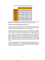
The main display of the clock should show the time in normal binary format.
To do this, the clock should display the time of day in binary code. Although
this is the main display, a digital readout of the binary time should also be
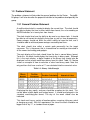
displayed so that anyone could learn binary from this clock. Table 1.3-1 below
shows an example of how to calculate a value from binary code. Note that
only positions that have a value of “1” are calculated into the numerical value.
Table 1-1 - Binary Code Example
Displaying the day, month, and year should be an option for this clock. This
can be done in both digital and analog format. It should be displayed in the
standard, month/day/year format. The day of the week should also be
indicated.
This clock must have a variety of location options, meaning sitting on a desk
or hanging on a wall. With this requirement, the size of the clock should be no
bigger than 8” by 11”, a standard sheet of paper.
8
The physical appearance should also be attractive to the target consumer. It
should have a “cutting edge” technology look that keeps with the “geek
theme” for this clock. It should offer a variety of geek themes, and a
personalized geek touch.
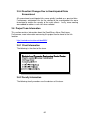
1.3.2 General Solution Approach
The clock will be made of two main displays. The primary display will show
the binary times, and the secondary will be the digital displays like other
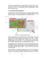
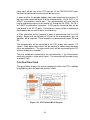
clocks. See Figure 1.3-1 below for pictorial of the design for solution.
Figure 1-1 - Design of geek binary clock
The primary display of the time will be done in the binary format. It will show
the time, day of the week, and date. These can be seen in Figure 1-1 as parts
labeled (1), (2), and (3) respectively. To accomplish this, an array of light
emitting diodes (LED) should be used. These will light up in a pattern
according to what the current time is. There should be seven LED’s for the
day of the week, lighting up one for the respective day of the week.
The secondary display, showing the time and the date (month/day/year) will
be in digital format. This will be shown on a multi-line/multi-character display.
The date will be figured into the program which should be built with C using
the fourteen possible calendar years. Figure 1-1item (4), shows the
secondary display.
Since the clock has the capability of displaying the time in either twelve-hour
or twenty-four hour format, a toggle switch will be used to switch between
formats. For the twelve-hour format an AM/PM indicator such as an LED will
9
be used to notify the user of the format being used. Figure 1-1, item (5) shows
this.
For this clock to be used as an alarm, a function programmed in C will be built
in for this capability. It will send out a noise at the set alarm time. Figure 1-1,
item (6) shows the alarm control buttons, which will perform standard alarm
functions such as: sounding at a designated time. Figure 1-1, item (9)
represents the location of the buzzer. Other possibilities if time, material, and
funds permit is a snooze function, a generated voice stating the time, and
specific time increment alarms, such as every fifteen or thirty minutes.
The program will also compensate for daylight saving times (DST). It will
automatically correct itself at the designated time of the years. This will be
built in the program with the fourteen possible calendar years. The DST
function will have a toggle switch that when on will auto-correct itself, or when
off, the user will correct it. This is an included feature for areas of the country
that do not observe daylight savings. Figure 1-1, item (7) depicts the DST
toggle switch. This slide switch may be located in the front, back, or top of the
unit.
It will also self-correct itself for leap year using the standard fourteen possible
calendar years. This should be done in the software of the clock. The clock
will not correct itself for century leap years.
The main power supply will be an AC source of 120V that can be plugged into
any standard United States wall outlet. The clock will have a transformer and
an AC/DC rectifier to provide a 5V DC source. Figure 1-1, item (8) depicts the
location of the AC voltage input.
To ensure that a power outage will not affect the clock’s time keeping a
standard 9V battery will be used for backup. This will allow for at least two
hours of running time. Figure 1-1, item (7) represent the battery location.
During a power outage the primary and secondary displays will turn off, but
the internal clock will keep running to conserve energy. When power is
restored to the clock, both displays will return on with the correct time. A 3mm
LED located in the front of the unit will indicate whether or not the clock is
operating on battery backup.
In addition to the battery backup LED, an alert will appear on the secondary
display signaling when the battery is low and needs to be replaced. Figure 11, item (5) shows this alert.
The appearance of the clock should appeal to the target audience, geeks.
The shell/case of the clock should be made of a hard yet light material that is
semi-transparent such as plexiglass. This will allow the user to see the wiring
and “electrical make-up” of the clock. An option to have the shell a standard
black plastic should also be available.
10
A personalized option should also be available. This could include engraving
the person’s last name or nickname on the front top of the clock. The colors
of the LED’s used for each function can also vary according to user
preference and the available options.
1.4 Operating Environment
The operating environment is limited to indoor places. The environment should be
able to supply the appropriate power needed through a regular wall outlet. It should
not be used in areas that contain a lot of moisture such as the bathroom or pool
room. It should not be in an area that it could potentially be dropped in a sink such
as a kitchen or laundry room. It should be limited to places such as bedrooms, home
offices, and in the work office.
1.5 Intended User(s) and Intended Use(s)
This section details the intended user(s) and intended use(s) of the project.
1.5.1 Intended User(s)
The intended user(s) are those who know binary code and fit the geek
persona. It can also be used by those who would like to learn binary through
a practical application. This should not be used by children due to certain
dangers such as small parts and electrical components.
1.5.2 Intended Use(s)
This object is a clock meant to display time primarily in binary with LED’s. It
provides other functionalities that are closely associated with a geek
personality. It is also intended to help individuals learn binary by using the
secondary display of the digital readout of the binary.
This clock can also be used as a standard alarm clock as well. It will sound at
a designated time by the intended user.
1.6 Assumptions and Limitations
The following part of the document will provide the assumptions and limitations that
the group has made/encountered with the project.
1.6.1 Assumptions
This section describes the assumptions of the project.
•
LCD display
11
The size and physical capabilities of the LCD display will have the
ability to meet the project’s requirements.
•
DST and leap year
The clock will be receiving a low frequency transmission to update itself
for daylight saving time or leap year. It will also be self-correcting for
time discrepancies. This function will have the ability to be disabled.
•
“Geeky” appearance
The outer shell of the clock will be made of a hard, semitransparent
material such as plexiglass.
•
LED’s
There will be several sets of lights on the clock’s exterior. The first set
of lights will be a horizontal set of seven lights indicating the day of the
week. The two other sets of LED’s will display the time in binary format
and the date in month, day, and year format.
•
Location and operating environment
The clock will only operate on a typical 120VAC, 60Hz outlet. The
clock is meant to be used indoors.
1.6.2 Limitations
This section describes the limitations of the project.
•
Features
The clock must have an alarm function, be self-correcting for daylight
saving time, have a battery backup, and be able to display time in
twelve and twenty-four hour formats. The twelve hour format must
have an AM/PM indicator.
•
Costs/Budget
The clock cannot cost over $150 in parts. Labor will not be counted in
the final costs.
•
Size and Weight
The size and weight will be a limitation in the project. It is intended to
be small enough to be put on a small table, and it also has to be light
enough to be wall mountable.
12
1.7 End Product and Deliverables
The following part of the document will discuss the end product and other
deliverables that will be included with the prototype at the end of the project.
1.7.1 Expected End Product
The geek clock will be a hybrid model based off existing binary clock
structures. Its exterior shall reflect that of the intended audience. Its overall
appearance will be a blend of technology and elegance. The idea behind the
project is to build a device that incorporates “geeky” features, but at the same
time, have an end product that is useful and practical to everyone.
The clock will display time in both twelve and twenty-four hour formats. These
times will be displayed digitally and in binary, respectively. The clock will
incorporate daylight saving time and leap year correction. It will display the
day of the week as well as date, month, and year information. In addition, it
will also have an alarm feature.
1.7.2 Deliverables
Along with the clock prototype, there will is also a user’s manual. This manual
is designed to assist the user in operating the clock’s many features. It will
include information on all of the features discussed previously as well as a
detailed description of their operations. The manual will also include a
troubleshooting section designed to help the user as much as possible if
he/she incurs a problem.
13
2 Project Approach and Results
The second section of this document provides the project approach by the group.
This includes the functional requirements and several consideration sections
including: functional requirements, design requirements and constraints, approaches
considered and chosen, design description, implementation process, end product
testing, and end product results.
2.1 Functional Requirements
This section will describe in detail what the clock’s features will and will not be.
Below is a list of its functions as well as a brief description of each one.
•
Power
The clock will be powered by a standard 120VAC outlet. It will also
have a battery backup which will maintain accurate date and time
information in the instance of a power outage.
•
Alarm function
The clock will have an alarm function integrated with its time function.
This alarm will sound through a small speaker. The clock will not be
equipped with an AM/FM radio function. The alarm feature will have
the ability to be turned on and off based upon user preference.
•
Displays
The clock will display date and time information in both digital and
binary formats. The digital display will also have the ability to be
enabled or disabled upon user preference.
•
Date/Time format
The clock will display time in both twelve and twenty-four hour formats.
The twelve hour format will have an AM/PM indicator in the form of an
LED. Also included with the actual time information will be month, day,
and year information. This will also be represented digitally and in
binary format.
•
DST and leap year
The clock will use a very low frequency receiver (VLF) to gather date
and time information. The clock will automatically update itself through
this transmission. It will be self-correcting for both DST and leap year.
It will also be self-correcting for any time discrepancies that may occur.
14
This feature will have the ability to be disabled based upon user
preference.
2.2 Resultant Design Constraints
This project has a few key constraints that need to be addressed derived from the
assumptions and limitations. There are a few design and software constraints as
well as physical and operating limitations.
2.2.1 Overall Constraints
•
Weight
The clock’s weight must be such that it can be wall mountable. Its size,
therefore, must also be accommodating to such a circumstance. Its
final weigh shall be no more than two pounds.
•
Maximum Size
The clock itself cannot be incredibly large or bulky. It shall be not
larger than 8” x 11”. The idea behind the project is to make final
product that is both multi-featured yet visually appealing.
•
Cost
The cost of building the clock must not exceed $150. It is important to
choose parts carefully keeping in mind that there is a limited budget.
2.2.2 Software Constraints
•
Twenty-four / twelve hour time formats
The clock needs to be able to display time in both twenty-four and
twelve time formats. The twelve hour time format needs to have an
AM/PM indicator as well.
•
Daylight Saving Time / Alarm Functions
These two features described in previous sections must have the
option to be disabled upon user request. Though these features
maybe helpful for some people, they are not applicable to everyone.
2.2.3 Physical/Hardware Constraints
•
Power
The device is intended to operate on a typical 120VAC residential
outlet. It is not designed to operate on a 220V source. There will also
15
need to be an onboard power supply in case of power failure. This
backup power source will provide power to the clock for at least two
hours.
•
Operating Atmosphere
This device is not intended to be used outdoors. The device will not be
waterproof, and it will not be designed to withstand adverse weather
conditions.
2.3 Approaches Considered and the One Chosen
The following section pertains to the multitude of options available to engineers for
designing and implementing a small project such as a binary alarm clock. There are
always multiple ways of approaching an engineering problem. Several aspects of
the project can be broken up into problem solving sections such as layout, software,
hardware, and power consumption. Each section will describe the approaches
considered, advantages and disadvantages, the one selected, and why it was
selected.
2.3.1 Binary Display Approach Considered and Chosen Result
Approach Considerations
The most pertinent question that arises when considering technology for
designing and implementing a clock is: How will the time and date be
displayed in binary? The Geek Binary Alarm Clock requires time to be
displayed in binary format. The initial technological consideration is LED’s.
LED’s are the natural choice because of their relatively low power
consumption and ease of integration onto a PCB.
Other technologies considered for display binary display were physical
switches, small light bulbs, LCD (liquid crystal display), and numerous other
light producing sources. Physical switches were immediately excluded
because the necessity to automate changes in states. Small light bulbs can
be thought of as bigger versions of LED’s. The size limitations and aesthetic
requirements of the binary clock exclude the use of small light bulbs. LCD
screens are also considered for representation of binary digits. Most digital
electronic clocks utilize this technology which is why it is better suited for
standard display rather than binary display.
Chosen approach
The requirement to represent binary digits (on/off states) finalizes the decision
to use LED’s. They also offer a wide variety of selection for the consumer.
16
2.3.2 Weekday Display Approach Considered and Chosen
Result
Approach Considerations
In order to display the day of the week electronically, another method is
needed. In order to display the time in standard format a large, electronic
array of changeable letters is required.
The two technologies were
considered for this job: a LCD display and an array of LEDs.
Chosen approach
It’s been chosen that an array of letters, S M T W Th F S, will be placed at
the top of the clock with respective single LED’s associated with them due to
the lower implementation cost and increased geek appearance.
2.3.3 12/24 Time Display Approach Considered and Chosen
Result
Approach Considerations
LCD screens provide an enormous amount of malleability with respect to
displaying alphanumeric information. LCD’s also allows both twelve and
twenty-four hour times to be displayed without difficulty. LCD’s are easily
manipulated in programming, offer almost unlimited versatility in alphanumeric
display, and are relatively inexpensive.
Another technology considered for displaying standard time is the mechanical
flip displays of older clocks. These displays consist of multi-sided plastic
chips in loops that flip mechanically to show the correct time. The first
problem is the fact that the clock would be incapable of displaying twenty-four
hour time. Switching between twelve hour and twenty-four hour would also be
difficult. Another technology considered for displaying standard time is a
small computer screen. This idea is an entire project within itself but is a
viable option given enough time and money.
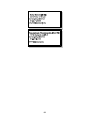
An alternate technology considered for displaying standard time is an analog
display. This would be a very simple technology to implement but would not
be very flexible. Like the mechanical flip display, the analog display would be
incapable of displaying twenty-four hour time. The standard hour label of an
analog clock could be pulled out and replaced like the following image in
Figure 2-1. This clock looks somewhat convoluted and unprofessional.
17
Figure 2-2 - Analog 12/24 Display Option
The last technology considered is an audible announcement of time. This
concept will be considered as an optional extra feature because it presents
many problems. These problems include the frequency of announcement,
alternation of twelve and twenty-four hours, and implementation requirements
such as loudness, voice, and speakers.
Chosen approach
The project proposal requirements does not require the standard display of
time to be in digital format but, in order to preserve the “geek” concept of the
project and the easy of implementation, a digital display such as an LCD
screen was chosen.
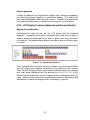
2.3.4 LED Size and Color Scheme Approach and Chosen
Results
Approach Considerations
LED’s come in a wide variety of sizes, colors, and material. The approach that
the project required for the display was to be seen at a glance (like any clock),
thus larger and brighter LED’s are preferred. This statement contradicts the
size of unit the whole clock needs to be. The LED’s must be a decent size for
one to see the time at a quick glance at the clock, but not large enough to
inhibit the size mentioned in the functional requirements. The LED’s must also
be spaced far enough away from each other for one to distinguish each LED
from the other, thus the design should use a smaller LED size. The group
chose to use two different sizes of LED’s larger LED’s (5mm) for the date and
time functions that would need to be looked at a glance. Smaller LED’s (3mm)
were chosen for the lesser used functions such as week notification LED’s
and ON/OFF LED’s that only need to be looked at occasionally.
Originally the color of the LED’s were just all going to be either green or red
because these were assumed to be the most accessible and easiest to read.
The group decided against limiting the LED colors to just those two because
they do not offer a sense of personalization to the project. The group also felt
18
that those colors are used quite frequently in the technology/electronic field
and would like some variety. The color of the LED’s has been preferred to be
customer specific, meaning that each customer can pick the color for their
LED’s from the color availability list below.
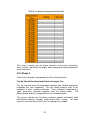
The group also decided to use ultra bright and superflux type LED’s for the
date, time, and day of week LED’s. These will increase the brightness of each
LED and will make it easier for the user to read. The tables below shows a
schematic of an ultra bright LED compared to a regular LED. Notice that the
ultra bright LED uses less voltage and has an higher wavelength intensity.
Table 2-1 - Regular LED
Table 2-2 - Ultra Bright LED
Figure 2-3 - Regular LED
19
Figure 2-4 - Ultra Bright LED
There are some limitations for this. One is that the date, time, and week
notification LED’s must be different colors so that the sections can be placed
closer together to keep the size of the clock down. It would also provide an
ease for the user to look at the clock and be able to see a distinct difference
between each LED field. The ON/OFF LED’s would also have a similar
limitation based on their available colors.
The ON/OFF notification LED’s were designed originally to be single color
LED’s that would light up when ON and not light up when the function it
represents is OFF. The group felt that this had many flaws in it because
during testing faulty LED’s would be harder to detect. Or if the user has the
switch constantly in the OFF position, they would never know if the LED
worked or was broken unless they turned it to the ON state. The group
decided a bi-color LED would be preferred. These LED’s would show one
color for an ON position and different color for the OFF position. It is varied by
voltages. The following shows the specifics of the bi-color LED’s for the
red/green option.
20
Table 2-3 - Operating characteristics for Red (MDK) and Green (VG) bicolor
LED’s
Figure 2-5 - Differences in Intensity graph
Chosen approach
After careful evaluation, the group decided that based upon availability, cost,
and ease of implementation, it would be better not to use a bi-color LED in the
end product. By using simple logic, the user would be able to determine
whether or not the LED’s are functional.
21
Finally the group has come up with the list of available options for the LED’s in
the display. It has been put all together in the following table.
Figure 2-6 - Available color options for each clock display section
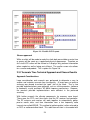
2.3.5 Layout Approaches and Results
Approach Considerations
For designing the layout of binary clock, two major approaches can be
considered. One approach is that the layout of the clock is to favor aesthetic
value rather than purely functional value. The other is the reverse of the first:
to use a minimalist approach and disregard aesthetics and any “bells and
whistles”. The following is a simple diagram of the proposed layout of the
front of the binary clock:
Figure 2-7 – Two basic proposed layout
22
Chosen approach
In order to implement the logic behind a digital clock, electrical components
will have to be merged together in a centralized location. This location will
then have to be placed inside a physical structure. Therefore, the team chose
the layout on the right due to its condensed yet simplistic size and layout.
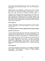
2.3.6 LCD Display Technical Approach and Chosen Results
Approach Considerations
Formalizing the layout to use with the LCD display took the following
approach. Determining what binary information that needs to be display in
decimal format was performed first in order to gather how many characters
are required. The following figure displays possible character utilization spots
in a series.
Figure 2-8 - Segment Possible Sizes
Then, arranging how are these character segments are to be placed within
the LCD display was executed to determine the number of rows needed.
Thus, Figure 3-8 displays 20 possible character utilization spots, with common
end sizes being highlighted with the dashed lines (i.e. 8, 12, 16, & 20).
Different layout combinations of these segments are also displayed within this
figure. However, only some of these combinations utilize the day display data
where others overwrite the displays when a low battery is present.
23
Figure 2-9 - Possible LCD Layouts
Chosen approach
While an effort will be made to make the clock look presentable no extra time
or money will be spent on a specialized physical appearance. Therefore an
8x2 sized LCD screen will be utilized as it displays only pertinent information
when needed as well as being cost efficient. The smaller screen also allows
for a smaller end product. This is option 6 in Figure 3-8.
2.3.7 Accurate Time Technical Approach and Chosen Results
Approach Considerations
Large consideration and research was performed to determine a way to
acquire and maintain accurate time functionality. A large focus on precise
accuracy was placed to extend the “geek” feel of the clock. Thus a few
possible implementations were gathered, such as utilizing counters (software
or hardware), crystal oscillators, AC 60Hz frequency conversions. However,
the previous possible implementations were deficient in the preferred
accuracy.
With further research the ultimate components for accuracy were found.
These were the RTC—real time clock—and the RF receiver and controller.
The RF antenna and receiver will work together to automatically gather
precise month, date, and time information from a low frequency radio
transmission called WWVB. This method of gathering data is often referred to
as RCC or radio-controlled clock. This radio transmission is also coded with
24
flags for leap year and daylight savings time. Given this radio transmission,
the clock will be able to automatically update itself in case of a discrepancy in
time keeping.
Although precise time information is gathered from the RF receiver,
maintaining this accuracy between updates is surmounted with the use of the
RTC. First of all, it does have a 32kHz crystal oscillator as well as a
adjustment function to correct the oscillator from slight variances in
accordance to the surrounding environmental temperature. Furthermore, this
component contains numerous other favorable characteristics. End of the
month calculations (28, 29 [leap year], 30, 31) for calendar updates, a low
power supple detection, and alarm interrupters functionalities are all provided
which will help reduce software coding. All information outputted from the
RTC will be sent to the microcontroller to decode and send to the subsequent
display and alarm components.
Chosen approach
Through implementation simplicity and high accuracy, the RTC and RF
receiver and controller was the chosen approach to acquire the highest
accuracy in time.
2.3.8 Microcontroller Technical Approach and Chosen Results
Approach Considerations
The “brain” behind the digital binary clock will be the microcontroller which will
control and direct all internal functions. The choice of microcontroller is an
important one which required much research. There are literally thousands of
microcontrollers resulting in many considerations. A digital clock requires a
basic microcontroller that has a minimum execution time, high amount of I/O
pins, is easily programmable, and is cheap. The large list of potential
microcontrollers suggested by faculty advisors and others found during
research were narrowed down to three selections: Intel 8051, Motorola
68HC11, and Microchip PICMicro microcontrollers. Further research was
performed on these three microcontrollers as well as inquiries from fellow
students.
Chosen approach
The final result, concurred by faculty advisors, was the choice of the PICMicro
family. Readily available from a faculty advisor was a PICMicro PIC16F877A
microcontroller.
The following is a picture of several PICMicro
microcontrollers in the PIC16 family.
25
Figure 2-10 - Microchip PICMicro microcontrollers – PIC16Cxxx
This chip was readily available, easily programmable, cheap, and had enough
I/O pins to complete the project. Senior design labs also have testing boards,
software, and other equipment specifically made for PICMicro
microcontrollers. The following is a grid of information concerning the chosen
microcontroller for this project, the PICMicro PIC16F877A. The grid is then
followed by a data sheet of this particular microcontroller. More specific
information on this family of microcontrollers is available at this link:
http://ww1.microchip.com/downloads/en/DeviceDoc/39582b.pdf.
Figure 2-11 - PIC16F877A Information Grid
26
Figure 2-12 - PIC16F877A Information Datasheet
2.3.9 Power Consumption Approach and Chosen Results
Approach Considerations
Power consumption is another topic for technical approach considerations. A
binary clock can consume energy is several ways. It can use solely a DC
power source, a local battery source, a mechanical device, or a chemical
reaction. It can also use a combination of these energy sources as implied by
the requirements and suggested in the project assumptions. Different
approaches to energy consumption are also limited by project assumptions
and constraints. The clock needs to be a small size, use little energy, and
look presentable.
One assumption has been established: the clock will require two different
power sources in order to ride through a power outage and one of these
sources will be from a DC electrical source. One approach to solving the
energy problem, the chemical reaction, is immediately seen as impractical. A
27
chemical reaction may refer to a gasoline engine or any combustible reaction
which creates energy. The energy consumption of a binary clock is not great
enough to warrant the use of such a source of energy. Therefore, the
approach of deriving and using energy produced from a chemical reaction is
ruled out. Another approach to the energy problem is a mechanical device. A
device which turns mechanical energy into electrical energy is called a
dynamo or, in general terms, a generator. Turning mechanical gears
physically is impractical because this project is not about the binary clocks
source of energy.
Chosen approach
Simplicity says to use the easiest form of energy available which is standard
DC power. The simplest and most readily available source of energy is the
electricity coming from the AC electrical outlets in a building. Of course, this
electrical energy may be regulated by equipment such as small voltage
generators available to electrical engineering students. The second source of
energy will have to be a 9V battery.
2.3.10 Backup Power Technical Approach and Chosen
Results
Approach Considerations
The power requirement in the project proposal is that the Geek Binary Alarm
Clock be capable of riding through a power outage for at least two hours. The
assumptions indicated that an independent battery source would be required
to power the clock through a power outage. The assumption is that the clock
will use a DC source from an electrical socket as the main source of power
and a local battery as the second.
The type of local battery is another technology consideration of the project.
There are several types of batteries available for implementation including
rechargeable cell batteries, PP3 (9V batteries), AAA batteries, AA batteries,
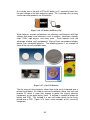
watch batteries, coin cell batteries, and other voltages. Below Figure 3-12
shows the many different types of batteries.
28
Figure 2-13 - Different types of batteries
Rechargeable cell batteries were rejected as an idea because of their relative
complexity. In order to implement them specialized circuitry would be
required to handle their regenerative properties. The two way nature of
rechargeable batteries makes them more complex.
Keeping it simple and emulating consumer clocks with “power ride-through”
features has shown that a 9V battery will be the easiest to implement. Many
consumer clocks on the market today possess internal battery compartments
for nine-volt batteries. The choice of battery to be used depends on several
factors. The power generated from the different classes of non-rechargeable
batteries and relative size will determine the selection. Also dependent is the
amount of power consumption from the binary alarm clock. The following is a
small grid of alkaline battery options, sizes, and voltages, amp hours, and
weights.
Table 2-4 - Battery Statistics
29
As it can be seen in the grid, a PP3 or 9V battery as it’s commonly known has
the most voltage in the least amount of space. This is perhaps why so many
smaller consumer products use 9V batteries.
Figure 2-14 - 9V Battery and Barry Clip
Watch batteries and coin cell batteries are extremely small batteries with high
voltages that power small electronics such as watches, calculators, memory
chips, PDAs, mp3 players, and many more. These batteries have the
advantage of being small and powerful. Many of them can produce voltages
greater than household batteries. The following picture is an example of
some of the coin cells available today.
Figure 2-15 - Coin Cell Batteries
The flat nature of these batteries allows them to be easily integrated onto a
printed circuit board. As visible on some of the batteries above, coin cells can
produce 3V which is more than enough to power the internal electrical
components of the digital binary clock. A method is needed to bridge the
battery and PCB. This method is a coin cell holder which can be easily
placed onto a PCB. Figure 3-14 shows some examples of this necessary
component.
30
Figure 2-16 - Coin Cell Battery Holders
Chosen approach
The group’s initial intention was to use the coin cell battery with a small
aluminum holder, but the advisors recommended otherwise.
Due to
availability and ease of use issues, a 9V battery has been selected for
implementation.
2.3.11
PCB Technical Approach and Results
Approach Considerations
The immediate consideration is a PCB. A PCB is the industry standard for
coupling electrical components such as resisters, capacitors, inductors,
microchips, memory, and bus lines. Another consideration is a breadboard.
A breadboard is a thicker, plastic version of a PCB with a single sheet of
connecting metal underneath. This sheet of metal conducts electricity through
components and does not require soldering.
Figure 2.2.2: Different PCBs and breadboards
31
Multiple types of PCBs exist such as single sided, double sided, through-hole,
grid layout, and others. This simplest type of PCB that fulfills requirements
will be used for this project. A single sided, through-hole PCB measuring
close to the size of a standard photograph will be used. The through-hole
technology will allow for easy integration of electrical components. A PCB of
this type can be purchased for less that $5 at any electronics store such as
Radio Shack.
Chosen approach
Because the bulky, unattractive, and unprofessional (breadboards are usually
used by beginners) look of breadboards, a PCB will undoubtedly be used.
The following figure depicts different types of breadboards and PCBs.
2.3.12
Casing Technical Approach and Results
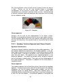
Approach Considerations
One of the requirements in the project proposal is that the Geek Binary Alarm
Clock end product be placed in an attractive case. There have been multiple
ideas for material and casing. Different technologies have been considered
including using the casing of an old clock, plastic casing, plexiglass, and
metal. The idea of encasing the end product in a metal casing was
immediately eliminated because of the clocks electrical properties. A nonconducting material would be preferable. A metal casing would also
significantly add to the weight of the clock is thus undesirable. The use of
metal such as aluminum or steel is also impractical because of cost. Metal, in
general, is more expensive to produce, manipulate, configure, and maintain
than plastics. This is the reason why many electrical components in the
technology industry are made with light-weight plastic polymers. Designing
the layout of a binary clock may also require a specific shape and construction
of a shell. In example, LED’s may be placed vertically or horizontally based
on preference. Manipulating a metal casing would undoubtedly be more
expensive than plastics.
Another, somewhat primitive technology considered for implementing the
casing of the binary clock is removing the casing of an old clock. The
advantage of this method is the cost. An old clock can be found for little or no
cost. The disadvantage would be the inflexibility of the casing. In order to
implement a clock to specific desired specifications a custom casing would be
most suitable.
The final two technologies considered for the casing of the binary alarm clock
are plastic and plexiglass. Local hardware stores such as Lowe’s or Home
Depot have many varieties of plexiglass available to customers. These
hardware stores even offer to cut plexiglass to meet customer’s needs.
Lowe’s stocks a transparent blue plexiglass measuring approximately 24” x
32
36” at varying thickness which may be cut into six pieces to form the sides of
a clock.
Plastics are the last and smartest choice in technology
considerations for the casing of a binary clock. Plastic is cheap, easily
manipulated, easy to maintain, and fairly shatter resistant. Seeking the help
of materials engineers and onsite production labs may prove useful to finding
the most adequate casing.
Figure 2-17 - Plexiglass
Chosen approach
Plexiglass will be used for the implementation of the clock’s exterior.
Plexiglass casing would also allow the clock to have a more “geeky structure”.
The user would be able to view all the inner workings and circuitry of the clock
that they find interesting. They would be able to see exactly how the clock
worked.
2.3.13
Hardware Technical Approach and Chosen Results
Approach Considerations
The design of overall hardware integration can take multiple approaches. The
most popular approach for engineering is the top-down approach. In the topdown model a general overview of the project is formulated without describing
any specific details. Each part of the project is then refined by designing it in
more and more detail. The opposite of this engineering process is the
bottom-up approach. The bottom-up method involves designing individual
parts of the project in specific details. These parts are then linked together to
form larger components. The process is repeated until the whole project is
completely formed.
Chosen approach
The hardware approach for the Geek Binary Alarm Clock will be the top-down
approach. The overall layout of the clock will first be designed. The individual
components will then be divided among group members who will then
individually design the specific details. After these individual pieces are
completed the binary clock will be assembled from its constituent components
to form the final end product. The preferred approach to designing and
33
implementing a binary clock will be top-down and from scratch. Senior design
requirements would also prefer that the project be approached from a uniqueto-a-group approach.
2.3.14
Software Technical Approach and Chosen Results
Approach Considerations
This section on technology consideration to be discussed is software.
Software can be written in many languages, some appropriate for certain
high-level tasks while some are appropriate for lower-level tasks. The aspect
of technology consideration in this section is concerned with choosing the
correct language, development environment, and coding implementation for
writing the software to a binary clock.
The options for languages include C, C++, Java, Visual Basic, and many,
many more. The indented use of a programming language will help to sway
the considerations for which language to choose. Questions may be asked
like: is this a high-level or low-level project? Will highly specialized functions
and reference libraries be required? Should a fairly flexible language be
chosen for maintenance and updating purposes? In order to answer these
questions the project needs to be looked at from a computer engineer’s
perspective. The pertinent question a computer engineer would ask is: how is
the software supposed to function with respect to the hardware? The answer
is that procedural coding will communicate with hardware such as LED’s and
LCD’s to produce on/off states.
An object-oriented procedural coding approach should be used. This
essentially describes the language to be chosen. Visual Basic is immediately
eliminated because there is no GUI involved with the clock and VB is
incapable of low-level communication. Java is another high-level language
specifically made for consumer electronics. It is a viable option but may
present difficulty when attempting low-level operations. C++ is much like Java
in its high-level attributes. The best foreseeable option for a programming
language is C. C is a language in between low-level and high-level. It will
give a programmer low-level access while being able to utilize high-level
functions to implement logic needed for a binary clock with many extra
features.
Chosen approach
The final result for programming language is the C programming language. C
has a reputation for handling pointers and memory well. This will aid in the
communication of hardware components. The integrated development
environment to be used is MPLAB. MPLAB is freeware available to students
in the senior design lab and is specifically designed to work with PICMicro
microcontrollers.
34
2.3.15
MPLAB Software Approach
Approach Considerations
Approaches in software are far less in-depth than most aspects of the project
because of its relative simplicity. Implementing a 12/24 hour clock with
corresponding on/off states and a list of extra features will require very little
designing and planning. The difficult part of the project dealing with software
is its integration with hardware. Technical approaches in software include
procedural, object-oriented, and modular programming. Procedural and
object-oriented programming techniques will undoubtedly be used in the Geek
Binary Alarm Clock project.
Chosen approach
Procedural programming will be used to break apart different functions of the
clock. For example the following code will return a string value representing
the day of the week:
/*Return the day of the week in string format*/
String dayOfWeek(clock input)
{
String ans=””;
ans = input.dayofweek();
return ans; }
Procedural programming is a technical approach that almost goes with the
need for saying. It is a basic requirement of programming and greatly will
help organize values used in the software written for the binary clock. Objectoriented programming is another basic technical approach where data in
encapsulated in virtual “objects” manipulated by specific procedures.
Because a binary clock will have many values that need to be monitored such
as on/off state variables for LED’s, object-oriented programming is a must.
An approach to software will require a medium in which to write code whether
it be Visual Studio, Metroworks CodeWarrior, or notepad for that matter. The
IDE to be used in this project will be MPLAB because of its close relation to
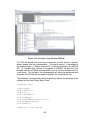
PICMicro microcontrollers. Here is an example snapshot of the MPLAB IDE:
35
Figure 2-18 - Example screenshot from MPLAB
This IDE will provide the necessary environment to write and test software
before loading into the microcontroller. The overall process is described in
the following steps: (1) Obtain a blank PIC, (2) write a program in the MPLAB
IDE, (3) Compile and simulate the program in MPLAB, (4) load the final
program onto the PICMicro microcontroller, and (5) test the microcontroller in
a real circuit. The testing of the microcontroller will mainly be performed with
help from the IDE and the test board available in the senior design lab.
The following is some pseudo-code that generally reflects the operation of the
software for the Geek Binary Alarm Clock.
#include<files>
//prototypes
void checkUI();
void init();
void aquireOSC();
void sendOSC();
void aquireReceiverIC(int ctr);
void sendReceiverIC();
void buzzer();
//declare a time counter
36
int counterForReceiverIC;
int main()
{
init();
//enter superloop
while(1)
{
//check for user input
CheckUI();
//perform necessary changes
aquireOSC();
//process OSC
//acknowledge receipt
sendOSC();
//piezo alarm buzzer code
if( //trigger alarm )
buzzer();
//get time update form ReceiverIC
aquireReceiverIC(counterReiverIC);
sendReceiverIC();
counterReceiverIC++;}
}
2.4 Detailed Design
Another large section of this report is the group’s detailed design for the project. This
section describes the project’s parts including a master table. It also includes a
detailed description table to describe how each part is used for the project’s
completion as well.
2.4.1 Summary of Material part usage
The following sections describe the main component for this project.
Furthermore, the following table provides an image of the component as well
as other specific details, such as manufacture/vender, part number, and cost.
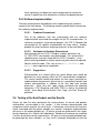
2.4.1.1
Microcontroller
The microcontroller is the “brains” of this device. It has an 8-bit
architecture with 14 Kbytes of Enhanced Flash memory. The amount
of Data EPPROM is 256 bytes and the amount of RAM is 368 bytes.
37
2.4.1.2
Real Time Clock
This IC is used for multiple functionalities, primarily accurate time
keeping capability for the clock. It utilizes information from the radio
frequency receiver to initialize the time. An internal 32 kHz crystal
oscillator is provided to maintain this time, as well as clock adjustment
function to correct the oscillator slight variance in accordance to
environmental temperature. Additional features provided are calendar
updates for leap year calculations up to the year 2099, low power
supply detected, and alarm interrupter. All data will be sent to the
microprocessor to separate the output data.
2.4.1.3
Receiver IC
The receiver IC will accept the incoming coded WWVB broadcast and
send the information to the microcontroller for decoding. The
information present in this coded signal will provide the clock the ability
to self-update day and time information.
2.4.1.4
Antenna
This antenna is specially tuned to receive a 60 kHz, low frequency
transmission called WWVB. This antenna will deliver the coded signal
to the receiver IC.
2.4.1.5
LCD Screen
This is a LCD panel for displaying the time, date, alarms, and low
battery information. The display is of two lines by eight characters
which can display numerals, letters, and symbols.
2.4.1.6
LEDs
This is a light emitting diode (LED) that will be used for the displaying
the date, time, and day of the week in binary format. As shown in the
approach, the date and time will be in 5mm size and the day of the
week will be in 3mm size. The LED’s will be powered a 5V DC source.
During a power outage, when the battery is running everything the
LED’s will not have power supplied to them to conserve energy for the
rest of the clock.
2.4.1.7
Piezo Buzzer
This is a sound device which will emit a buzzing sound at a user
defined alarm time setting.
38
2.4.1.8
AC/DC Converter
An AC power cord connected to an AC/DC converter will provide a
5VDC power supply to the clock.
2.4.1.9
9V Battery and Harness
A 9V battery will be connected as a secondary power source. This
provides backup power functionality for the device.
2.4.1.10 Buttons and Switches
Pushbutton and slide switches will be used as the user input devices
for the clock. Five pushbutton switches will be used and 3 slide
switches will be used.
39
Table 2-5- Component information
40
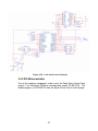
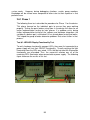
2.4.2 Block Diagrams of Design
Figure 3.1 presents a high level block diagram of the binary/digital geek clock
where as Figure 4.2. presents the circuit schematics of this device.
Figure 2-19 - Geek clock block diagram
41
Figure 2-20 - Geek clock circuit schematic
2.4.3 PIC Microcontroller
One of the hardware components to be used in the Geek Binary Alarm Clock
project is the Microchip PICMicro microcontroller model PIC16F877A. The
following figure is a PIC16F877A from the 40-pin Plastic Dual In-line Package.
42
Figure 2-21 - Top-down pin layout view of PIC16F877A
The microcontroller has an 8-bit architecture with 14 Kbytes of enhanced flash
memory. The amount of Data EPPROM is 256 bytes and the amount of RAM
is 368 bytes. The most important aspect of the microcontroller is it’s input and
output. The PIC16F877A has 33 I/O pins: RA0-RA5, RB0-RB7, RC0-RC7,
RD0-RD7, and RE0-RE2. This section will attempt to address the physical
connections to and from the microcontroller. References to the hardware
block diagram will be made.
The first and foremost need of the microcontroller is electrical energy. The
PIC16F877A operates on a voltage between 2 Vdd and 5.5 Vdd. Input pin 32
will be used to deliver the voltage and pin 31 (Vss) will be grounded.
Input/output pins 2 through 7 corresponding to RA0-RA5 will be used to
connect the user interface module. The UI module will contain four binary
buttons for time, alarm, hours, and minutes and two on/off switches for LCD
display toggle and daylight saving time toggle. A total of six, unidirectional
signals will be connected to the microcontroller.
The real time clock (RTC) and receiver IC will also be connected to the
microcontroller. The RTC’s oscillator output will be connected to pin 13
(OSC1/CLKIN) on the PIC16F877A. The connection will be a constant,
bidirectional in order for the RTC oscillator to know the current time. The
43
clock signal will be sent to the RTC from pin 14 the OSC2/CLCKOUT port.
No direct connection to the antennae will be necessary.
In order to utilize the periodic updates from radio frequencies the receiver IC
will have to be connected to pin 26 of the microcontroller. Pin 26 (RC7) is an
USART asynchronous receive port. The microcontroller will send read to
receive and polling signals to the receiver IC through pin 25 (RC6). Pin 25 is
an USART asynchronous transmitter. A DR register containing data will be
read by one of the RC I/O ports. Asynchronous signals will be used because
clock updates do not need to occur synchronously.
A 52-bit connection will be required in order to communicate with the LED
display. Because of the limitation of I/O pins on the microcontroller, four 4:6
decoders will be required. These decoders can be connected to pins RB and
RD.
The microcontroller will be connected to the LCD display with requires 112
signals. More digital logic circuits will be required to communicate between
these two components. The logic circuits wires will be connected to pins RC
and any leftover pins available.
The final component connected to the microcontroller is the Piezo buzzer
which only requires a single on/off signal. The connection will be made at any
available I/O pin.
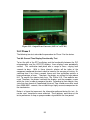
2.4.4 Real Time Clock
The figure below displays the internal components within the RTC in addition
to highlighting some the dominate features in blue.
Figure 2-22 - RTC Internal Block Diagram
44
2.4.5 Receiver IC and Antenna
The antenna will be connected to the receiver through pins 7 and 10. This
information will be processed and then sent to the microcontroller via pins 22
and 23.
Figure 2-23 – Receiver IC internal block diagram
2.4.6 Power
Below is a demonstration of the distribution of power to the different clock
components.
Regulated Power Supply Source
The primary power supply will utilize the 120 volt AC source from the
wall. The 120VAC source will then be input into the AC/DC converter,
and 5VDC will be output. This 5VDC source will be used to operate
the clock. The device allows for up to 1A of current, which exceeds our
requirements.
45
Figure 2-24- AC to DC Circuit Diagram
The secondary back-up power supply will utilize a 9V battery source in
case of a power outage, thus following the same setup as the primary
power supply source. The large current supply here is now not a
concern as in this mode the LEDs will be turned off.
Switching Circuit
To create a simple switching circuit, NMOS transistors were utilized.
Connecting the output from the PIC microprocessor to the gate of these
transistors will control the final signal going trough the transistor. Below, this
figure represents a simple case of this concept. When a 1V input is placed
both gate of the NMOS, then the input signal will pass through to the output.
This therefore simulates a short circuit. Furthermore, to obtain the switching
effect, when a 0V input is placed on the gate a degraded 0 will be produce.
Thus, this 0V gate input simulates an open circuit. Figure 5-7 graphically
displays this switching capability.
Figure 2-25 - NMOS signal functionality
2.5 Implementation Process Description
This section explains the implementation process and materials used for completing
the geek clock. The section breaks down the implementation process into two main
sections: hardware implementation and software implementation. Furthermore, this
section details some of the problems the team faced and how these problems were
overcome in developing the clock prototype. Suggestions for how the
implementation process might have been improved are also included in this section.
The materials used for the implementations were: breadboards, smartboards, LEDs,
LCDs, Buzzer, AC/DC converter, power supply, multimeters, oscilloscopes, CCS C
Compiler, and the HI_TECH PICC-Lite compiler.
46
2.5.1 Hardware Implementation
There were several problems the team encountered while implementing the
hardware aspect of the clock design; however, most were easily resolved.
The following sections provide details concerning the hardware
implementation.
2.5.1.1
Problems Encountered
The main problem encountered with the hardware implementation
encompassed the task of actually acquiring the desired hardware
components for assembly. Glitches in company search engines cased
difficulties purchasing red LEDs, where as other components faced
numerous backorders, particularly the LCD screen and the AC/DC
transformer. Furthermore, the team also faced the implementation
delay with the LED components as the first set of LEDs was rightangled and the second order of LEDs were lost after the shipping
process.
Another problem the team faced was building the enclosure case for
the clock. The team thought the material engineering department
would be of help with this aspect of the design, in which no availability
was provided in both the automation of the process or availability of
machinery.
The small stature and mountability of some of the components caused
some connection problems for the team. The team was unaware the
receiver IC and the RTC were surface mountable; thus, creating a
connection to the test breadboard temporarily unavailable.
2.5.1.2
Solutions for Problems Encountered
The solution to the main problem of acquiring components was
multifaceted. First of all, the team solved the backordered problem by
choosing different type of LCD screen with similar properties as the
original. The team also re-ordered the AC/DC transformer through
direct vender. These two actions allowed for a quick turnaround in
acquiring the previous parts.
Solving the problem encountered with the LEDs required more
interaction. First of, the supplier was contacted in order to verify if red
LED were actually unavailable since green and yellow LEDs were
available. The supplier provided the information of the part number to
the team which was needed for ordering the red, as well as the green
and yellow, LEDs. The lack of part information for the red LEDs was
due to the supplier’s component web search engine contain a filtering
glitch, which they are now aware of.
47
Furthermore, to face the other problem of the LEDs being temporarily
lost, the team carefully removed the special plastic casing of the rightangled LEDs and the leads were straightened out. This allowed the
team to test the integration of the software and hardware components
together as the replacement LEDs were being acquired. However, this
cause another problem the team faced since the LEDs’ casing had the
positive and negative labels for the leads. The team addressed this
problem by and reduced future confusion about the unmarked leads by
placing each of the LEDs in the bread board that oriented the LEDs in
a way to display which leads were positive and negative.
Also, to help quicken the time to acquire the needed part, numerous
components were purchased from our personal funding. With less
paperwork and no shipping, such parts were gathered immediately to
help with implementation.
Developing the enclosure casing for the clock was solved by looking
around campus and team member hometowns for replacement
machinery. After many unsuccessful options, the team was notified of
the location of a hand drill press within the senior design lab. Thus an
AutoCAD template was created, personal drill bits were purchased out
of pocket, and steady hand operation was performed to cut out the
holes needed in the casing. This took a significant amount of time.
Furthermore, a consequential problem from this solution was
encountered when the drill press was removed for a time period. The
group was not notified of such action until the team had asked about it
in a meeting. This slowed down the status of the final casing
implementation.
Due to the size of the slide switches used for setting the alarms and for
setting user preferences the group decided to have these mounted on
the back of the clock instead of the front. The team decided the front
would be purely for display purposes. The size of the LCD screen was
much smaller than expected so the casing layout had to be modified for
that as well.
2.5.1.3
Suggestions
Increased communications and more frequent updates on the progress
would have saved time during the development phase, as it was
pushed back. Many of the complication during the implementation
were due to lack of components or resources being available for use.
More foresight of such problems would have helped the team
determine a more accurate schedule.
Furthermore, the implementation process for the casing could be
improved it a software controlled drill press was available. This would
48
have significantly cut down the time the group spent to create the
casing. It would have also allowed for a sleeker end product design.
2.5.2 Software Implementation
The team encountered a few problems while implementing the software
aspect of the clock design. The following sections provide details concerning
the hardware implementation
2.5.2.1
Problems Encountered
One of the problems that was encountered with the software
implementation concerned the compiler for the PIC microcontroller. In
reference to previous senior design projects, the CCS C Compiler did
not compile on the specific microcontroller the team chose. Another
problem the team faced was acquiring resources of the need libraries.
2.5.2.2 Solutions for Problems Encountered
After attempts with the CCS C Compiler, another alternative, the
HI_TECH PICC-Lite compiler, was downloaded. This solved all the
compiling errors that were faced with the CCS C Compiler. Lastly,
online search provided the solution concerning what were the required
libraries and their code. Files such as the pic.h, 16F877A.h, and
delay.h were required for compilation.
2.5.2.3
Suggestions
Documentation or a tutorial within the senior design area would be
beneficial as many projects utilize the PIC microcontroller component.
This central location would help reduce the time spent searching for
implementation requirements due to lack of a centralized location and
concise documentation in addition to the little help from outside
professors. Much time was spent during contacting the following
companies, CCS, Microchip, and HIGH TECH, as well as the following
faculty, Jason Boyd, Steve Kavorik, Prof. Tyagi, and Prof. Zhang, for
guidance.
2.6 Testing of the End-Product and the Results
Details on how the team performed the testing phases to ensure end product
functionalities are described in this section. It also includes documentation and
acceptance criteria used for the set of tasks. Furthermore, to minimize the time/cost
factor associated with the project, periodic test intervals throughout implementation
will occur as the project progresses. All phase testing was preformed in the senior
design laboratory or in Coover Hall laboratories. Software or hardware was modified
if results do not meet design requirements. All types of testing mentioned below was
be performed by team members, as they have a thorough knowledge of how the
49
system works. However, during debugging situations, certain group members
knowledge will be utilized more compared to others due to their expertise in that
particular area.
2.6.1 Phase 1
The following three tests describe the procedure for Phase 1 for the device.
This phase focused on the individual parts to ensure they were working
properly. Testing the parts before using them in the design will allow for an
easier implementation testing for later phases. If a problem exists during
further implementation testing of the software and hardware integration, the
variable of a broken part is minimized if it has already been tested, and works.
This helped the group to better determine problems that arisen further in the t
process.
Test #1- LED/LCD Display Functionality Test
To verify hardware functionality amongst LEDs, they were first connected to a
power supply will test their ON/OFF functionality. Visually verifying the light
illumination from the LEDs was noted. LEDs that did not meet the illumination
functionality was discarded. Thus, the successful criterion was all of the
remaining LEDs illuminates when connected to a power supply. The following
figure showcase the results of this test.
50
Figure 2-26 - LED Illumination Functionality Test
The LEDs visual clarity with the plexiglass casing was also tested. They were
placed inside the holes cut out in the plexi-glass front part of the casing. This
tested to make sure that the viewing angle was not minimized by the
transparent casing. It also allowed the team to test proper intensities to
ensure that the light was not being absorbed by the plexiglass surrounding the
holes. The results of this section of test are presented in the two figure below.
Figure 2-27 - 5mm LEDs Within Casing
Figure 2-28 - 3mm LEDs Within Casing
Test #2- LCD Display Functionality Test
To verify hardware functionality amongst LCD screen, its connection to a
power supply and the PIC microcontroller will visually verify the
alphanumerical functionality. A simple string from the PIC microcontroller will
send all characters for each segment to the LCD screen. The
display/illumination from the LCDs was measured.
LCD screens that do not meet the illumination functionality will be discarded.
A successful criterion was the LCD screens that illuminate any character
when connected to a power supply and PIC microcontroller.
51
Figure 2-29 - LCD Screen in OFF State
Figure 2-30 - LCD Screen in ON State
Test #3- Power Functionality Test
Due to the multiple components associated with the device in which all require
power to operate, except for the antenna, the amount of voltage and current
provided by the converter was tested. Thus this test verified that all power
ranges are being provided will be preformed during this test. These voltages
was verified visually with a DMM—Digital Mulitmeter—in the laboratory. A
successful criterion was the AC power supply provides all necessary power
voltages to all components.
Table 2-6 – Power functionality testing table
52
Figure 2-31 - Output From Converter (120V AC to 5V DC)
2.6.2 Phase 2
The following two tests describe the procedure for Phase 2 for the device.
Test #4- Current Time Display Functionality Test
To test the drift of the RTC oscillatory and the functionality between the PIC
microcontroller and the LED/LCD displays, these displays were periodically
verified. This verification took place over a range of times, varying from
seconds to days. With in these intervals, photos will be taken of the
component compared the atomic clock to increase the accuracy of testing. As
switching time is less than a second, human real time verification contains a
large percentage of error. Therefore, the photos are utilized to help reduce
this. To acquire the atomic clock time, The Official U.S. Time website was
used. Therefore, the photos had both the displays and the computer screen
within the shots in order to compare the data. According to their website, they
state their time format of Coordinated Universal Time should never differ more
than 0.000 000 1 seconds; thus establishing a highly accurate comparison for
the clock device.
Below is a figure that represents the information gathered during this test. As
can be seen, two pictures were collected. These pictures were taken at the
tester preference as long as group member stayed within the time period.
53
Table 2-7 - Current time display functionality table
The success criterion was the device maintains the current binary time and
digital time (when applicable) on the displays, updating every second.
Test #5- Current Date Display Functionality Test
To test the drift of the RTC oscillatory and the functionality between the PIC
microcontroller and the LED/LCD displays, these displays were periodically
verified. This verification took place over a range of a few days.
With in these intervals, photos were taken of the component and compared
the atomic clock to increase the accuracy of testing. As switching time is less
than a second, human real time verification contains a large percentage of
error. Therefore, the photos were utilized to help reduce this. To acquire the
atomic clock time, The Official U.S. Time website was used. Therefore, the
photos had both the displays and the computer screen within the shots in
order to compare the data. According to their website, they state their time
format of Coordinated Universal Time should never differ more than 0.000
000 1 seconds, thus establishing a highly accurate comparison for the clock
device.
The figure below represents the data gathered and allowed the team to review
the results of the photos. As can be seen, four pictures will be collected at
set times to verify the precise switching date. Both midnight and noon is
collected to double check if errors occur.
54
Table 2-8 - Current date display functionality table
The success criterion was the device maintains the current binary time and
digital time (when applicable) on the displays, updating every second.
2.6.3 Phase 3
The following three tests describe the procedure for phase 3 for the device.
Test #6- Daylight Saving Time Adjustment Functionality Test
Due to the delay in acquiring part, this functionality test had to be modified.
The team missed the time constraint to have the prototype working by
October 29 to test the 2:00:00 crossover from daylight saving time to standard
time. Thus, the team was only able to test the user ON/OFF of DST
preference. Human visual verification will only be needed to view whether or
not the updates occur.
Table 2-9 - Day light saving adjustment functionality table
The acceptance criterion was the device adjusts the time and date on the
designated daylight saving dates preference when applicable.
Test #7- Alarm Functionality Test
55
To test the functionality between the PIC microcontroller, the LED/LCD
displays, buttons, and buzzer these components were periodically verified.
This verification took place over a range of a few options as can be seen in
the figures below. The first figure declares some of the set values (to test the
edges) for the alarms as well as allowing the tester with some personal
preference to set the random1-5 values (to mimic typical user usage).
Table 2-10 - Alarm table
Furthermore, these values were then tested according to the grid below to
determine whether multiple alarms caused unforeseen problems. Here,
human visual verification tested the displays update accordingly to the
tester/user alarm input. Also, the buzzer was tested to hear if the sound
started accordingly and if the volume is within reason. The tester used his/her
own hearing capability without the use of any blockers or amplifiers.
Table 2-11 - Alarm sound functionality table
The success criterion was the device correctly triggers the alarm display and
sound at the determined times.
Test #8- Battery Backup Mode Functionality Test
The battery backup mode functionality test occurred once all hardware and
software components were integrated into the system. Different time and
alarm combinations were tested to ensure minimum battery life when the
device was unplugged from the AC power supply. In the figure below, the
voltage output will be measured with the DMM at the defined time interval.
The test occurred longer than the minimum time interval to determine the final
time of backup power functionality.
56
Table 2-12 - Battery backup functionality table
The success criterion was the device maintains current time information,
alarm settings, and battery life display when operating on battery backup for
at least two hours.
2.6.4 Phase 4
The final test describes the procedure for Phase 4 of the device.
Test #9- Overall Functional and Structural Integrity Test
This test occurred once the end-product hardware and software component
integration was near completion. This was tested amongst eight to ten
individuals to aid in usability verification. These individuals comprised of a
“geek” personality; therefore, engineers were the primary target. The
following figure displays a composition of their recommendation.
The success criterion was the device maintains product functionality while
withstanding common everyday usage during these surveys. No major
concerns arise from these results, thus no redesign was needed.
57
To organize the results from all these four phases, the following two forms
shall be utilized. The Component Testing Form – gather all pertinent
information collected for each individual test – and the Testing Track Form keeps track of what tests were done and which were successes. All these
forms were kept in a logbook in the senior design locker and provided in an
easily viewable and concise document to review all testing information.
2.7 Project End Results
This section summarizes the final status of each major component of the endproduct. Much time and effort was spent in acquiring the need parts to implement
this project. The team now is working towards bring the project back on schedule in
sight on components still not available.
2.7.1 Hardware Results
All acquired hardware components were fully tested and functional with the
breadboards and smartboards. Furthermore, detail instructions on clock
utilization and replacement are presented in the completed user manual.
2.7.2 Software Results
Revisions of the software is currently being addressed for correct functionality.
Documentation concerning all code and revisions are provided in the Software
Requirement Document.
2.7.3 Overall System Results
Although the prototype is not fully implemented, once software progress, the
clock will be quickly constructed.
58
3 Closure Material
The last section of this report contains information regarding the overall assessment
of the project as well as a reflection on its work.
It discusses potential
commercialization options as well as recommendations for work in the future. Finally
it discusses lessons learned during the project lifetime as well as risk mitigation
information.
3.1 Project Evaluation
To successfully evaluate the project, different milestones were put in place to gauge
the success of the project. The first of these milestones was research. The project
team decided that the research portion of the project was excellent; above and
beyond. Many great ideas flowed from this section, and the team was able to pick
and choose from a wide variety of ideas. Next was the parts milestone. The team
ordered parts over the summer, and most parts arrived. After a few mishaps, all
parts were finally available in mid October. The group feels that this milestone was
met, but not exceeded. Hardware and software design were completed during the
spring 2006 semester. After important input from the project advisors, this activity
was completed satisfactorily. After hardware and software implementation and
testing is completed, the degree of success of the design work can be evaluated.
The team’s goal for total hardware and software integration is late November, early
December.
3.2 Commercialization
The group also toyed with the idea of product commercialization. After a careful
analysis of the parts and prices, it was determined that the clock could be built in
high volumes for a cost of about $25. The team then decided that a $40 price tag
would be associated with the Geek Clock. The clock would be marketed to
electronic retailers such as Best Buy, Walmart, Radio Shack, and technological
novelty shops across the US.
3.3 Recommendations for Additional Work
In addition to all of the work done during the year, the team has a few requests of
additional work to be done. First, the group would like to see some new features
added to the clock. A few of these features include character strings printing to the
screen on holidays and birthdays, a speaker and am/fm radio, and multiple color
scheme choices for the LED’s. In addition to new features, the group would also like
to see a streamlined case design. The prototype case was made by hand, and it’s
difficult to do. A streamlined case design would be taken care of in the
commercialization process.
59
3.4 Lessons Learned
This section describes some of what the group learned during the course of the
project. It entails the details of what went well and what did not go well, what
technical and non-technical knowledge was gained, and what changes the team
would do differently if the team were to do the project over again.
3.4.1 What Went Well
One thing that was done well was the budgeting of time. The group was
aware of time constraints and conflicting schedules and was able to work
together to overcome obstacles. The group also understood the breath of the
project extremely well, which helped the team create features above the
minimum requirements.
3.4.2 What Did Not Go Well
Now that implementation and testing is being done, the group realized that
part selection and availability was a big deal. Since there were a few
problems associated with parts, the group decided that it would have been
better to find a backup replacement to as many parts as possible to avoid
problems of back-orders and obsolescence.
3.4.3 Technical Knowledge Gained
During the project, the team was able to gain some valuable information
regarding hardware and software. Circuit development, PIC programming,
part interfacing, and testing practices were some of such gained technical
skills. Everyone in the group feels that they have benefited in both areas as a
result of this project.
3.4.4 Non-Technical Knowledge Gained
In addition to the technical skills acquired, the group also has learned valuable
management skills that will be useful throughout everyone’s career. Such
management skills include risk management, time management,
communication, team work, and documentation.
3.4.5 Changes
Now that everything is said and done, the only thing that could have been
handled better was the parts situation. Again, provided a backup part or
supplier to the primary would have been a good idea to help with the acquiring
of parts.
60
3.5 Risk and Risk Management
Finally, the group needed to take some risk mitigation steps to guarantee a
successful project. This section shall discuss the risks and how the team managed
those risks.
3.5.1 Anticipated Potential Risks
Many risks were anticipated by the team. Following is a list of such
anticipated risks and the management steps the team took to help minimize
the effects if such a risk should occur.
1. Blown components – Due to the nature of the project, many of the
components could easily be blown. Thus the current and voltage
levels were continuously monitored to ensure the component
maintain functionally within the data specs. Furthermore, the team
would order a few extra components just in case a component
would encounter this risk.
2. Loss of team member – Internships or family emergencies are a
common occurrence that would remove a team member from the
project. Therefore, the group took careful documentation steps,
such as shared knowledge to all members, to ensure a safety net in
case of such a risk.
3. Delay in part acquisition – The group implemented extra lead time
in scheduling for parts
3.5.2 Anticipated Risks Encountered and Risk Management
Many of the anticipated risks were avoided due to well executed of the
precaution actions. However, not enough lead time was forecasted due to
multiple delays in acquiring parts. The team resulted in purchasing backup
components, some even local vendor to help return the project back on
schedule.
3.5.3 Unanticipated Potential Risks
As with any project, there will be things that a group will encounter that they
didn’t plan on. For this project, the group ran into parts selection and
availability issues. These problems were taken care of quickly by finding
replacement parts, but it is an issue that could have been prevented by better
planning when submitting the parts list. In response to this problem, steps
have been taken to make sure that there are second and third options to
important steps in the project.
61
3.5.4 Resultant Changes Due to Unanticipated Risks
Encountered
All encountered unanticipated risks were quickly handled on a punctual bias.
Furthermore, anticipated risks for the solution to the unanticipated risks were
formulated to reduce the severity of the cyclic effects. Lastly, more meeting
were added to address such risks when needed.
3.6 Project Team Information
This section contains information about the Geek Binary Alarm Clock team.
Furthermore, more information concerning this project can be found at the link
location.
http://seniord.ece.iastate.edu/dec0604/
3.6.1 Client Information
The following is the client of the team.
3.6.2 Faculty Information
The following faculty members are the advisors of the team.
62
3.6.3 Student Team Information
The following students are the members of the team.
63
64
4 Closing Summary
This purpose of this project is to create a binary alarm clock that will incorporate
several fun and interesting features into it. The intent of this product is to blend in
with today’s technology. It is important that the design be sleek and compact,
ultimately appearing physically attractive.
Its outer shell will be made out of plexiglass. It will contain colored LED lights (red,
green, and yellow), and a digital readout display. On the front of the clock, there
will be a couple different sets of LED’s. The first set will be a horizontal set of
seven LED’s. This will indicate the day of the week. They will be yellow in color.
The next set of lights will display the month, date, and year in binary format. These
lights will be green in color. The final set of lights will contain the actual time,
again, in binary form. These lights will be the color red. Finally, there will be a
digital readout in addition to its binary time information. This will be an LCD
display. This feature will have the ability to be disabled based upon user
preference.
The clock will incorporate many special, “geeky” features. The first special feature
will include an alarm clock. This feature will involve a small onboard buzzer to
sound at the specified alarm time. The alarm function will be able to be turned on
or off as necessary. The next special feature that will be included is daylight saving
time (DST). This feature will automatically self-adjust the clock for daylight saving
time. Just like the alarm, this feature will have the option to be disabled. Lastly,
there is to be a reliable battery backup in case of a power loss. This feature will
provide power to the clock for a minimum of two hours after the outage has
occurred. The battery backup method will give the clock the ability to keep current
time/day information during the power loss. The clock will also contain a digital
readout in addition to its binary format. Most features will have the ability to be
enabled / disabled based upon user preferences.
65
5 References:
Fogie, Seth. Building a Linux-Driven Digital Picture Frame. 2006. 15 Mar. 2005. <
http://www.quepublishing.com/articles/article.asp?p=375500&rl=1>
Iguana Labs. Digital Clock. 2004. < http://www.iguanalabs.com/clock.htm>
Ivan. Building a picture frame – The “junk” –top revival. 2004.
<http://channel9.msdn.com/wiki/default.aspx/Channel9.JunktopRevival>
Kihara, Masami. Digital clocks for synchronization and communications. House:
Boston, 2003.
Marshall, Brain. How Digital Clocks Work. 2006.
<http://home.howstuffworks.com/digital-clock.htm>
Radio Shack. Cables, Parts & Connectors: Component Parts: Breadboards & IC
Sockets.
<http://www.radioshack.com/family/index.jsp?cp=2032058.2032230&categoryId=2
032265&pg=1>
Schildt, Herbert. C/C++ Programmer’s Reference 2nd Edition. McGraw-Hill
Publishing. New York, 2000.
SELTRIN Pre. Ltd. Fundamentals of Electronic Watches. General Printing &
Publishing Services Pte. Ltd. Singapore, 1980.
Haviland, Robert. Build-It Book of Digital Clocks. TAB BOOKS Inc. Blue Ridge,
PA. 1986.
Microchip.com. PIC16F877A. 2006.
<http://www.microchip.com/stellent/idcplg?IdcService=SS_GET_PAGE&nodeId=13
35&dDocName=en010242>
Morton, John. PIC Your Personal Introductory Course. Newnes. Boston, 1998.
Bergquist, Carl. Guide to PICMICRO Microcontrollers. Sams Technical
Publications. Indianapolis, 2001.
Predko, Myke. Handbook of Microcontrollers. McGraw-Hill Publishing. New York,
1999.
BEAM Pieces. Batteries Compared. 2006.
<http://www.solarbotics.net/library/pieces/parts_elect_pass_batcomp.html>
BatteryBob.com. Product Comparison. 2006.
<http://www.batterybob.com/category.asp?cat=9022>
66