1
Ham, R. E. et al. "Microwave Measurements" The RF and Microwave Handbook Editor in Chief Mike Golio Boca Raton: CRC Press LLC,2001 4.5 Theory of High-Power Load-Pull Characterization for RF and Microwave Transistors John F. Sevic In both portable and infrastructure wireless systems the power amplifier often represents the largest single source of power consumption in the radio. While the implications of this are obvious for portable applications, manifested as talk-time, it is also important for infrastructure applications due to thermal management, locatability limitations, and main power limitations. Significant effort is devoted toward developing high-performance RF and microwave transistors and circuits to improve power amplifier efficiency. In the former case, an accurate and repeatable characterization tool is necessary to evaluate the performance of the transistor. In the latter case, it is necessary to determine the source and load impedance for the best trade-off in overall performance. Load-pull is presently the most common technique, and arguably the most useful for carrying out these tasks. In addition, load-pull is also necessary for large-signal model development and verification. Load-pull as a design tool is based on measuring the performance of a transistor at various source and/or load impedances and fitting contours, in the gamma-domain, to the resultant data; measurements at various bias and frequency conditions may also be done. Several parameters can be superimposed over each other on a Smith chart and trade-offs in performance established. From this analysis, optimal source and load impedances are determined. Load-pull can be classified by the method in which source and load impedances are synthesized. Since the complex ratio of the reflected to incident wave on an arbitrary impedance completely characterizes the impedance, along with a known reference impedance, it is convenient to classify load-pull by how the reflected wave is generated. The simplest method to synthesize an arbitrary impedance is to use a stub tuner. In contrast to early load-pull based on this method, contemporary systems fully characterize the stub tuner a priori, precluding the need for determining the impedance at each load-pull state [1]. This results in a significant reduction in time and increases the reliability of the system. This method of load-pull is defined as passive-mechanical. Passive-mechanical systems are capable of presenting approximately 50:1 VSWR, with respect to 50 Ω, and are capable of working in very high power environments. Repeatability is better than –60 dB. Maury Microwave and Focus Microwave each develop passive-mechanical load-pull systems [2,3]. For high-power applications, e.g., > 100 W, the primary limitation of passive-mechanical systems is self-heating of the transmission line within the tuner, with the resultant thermally induced expansion perturbing the line impedance. Solid-state phase-shifting and attenuator networks can also be used to control the magnitude and phase of a reflected wave, thereby effecting an arbitrary impedance. This approach has been pioneered by ATN Microwave [4]. These systems can be based on a lookup table approach, similar to the passivemechanical systems, or can use a vector network analyzer for real-time measurement of tuner impedance. Like all passive systems, the maximum VSWR is limited by intrinsic losses of the tuner network. Passivesolid-state systems, such as the ATN, typically exhibit a maximum VSWR of 20:1 with respect to 50 Ω. These systems are ideally suited for medium power applications and noise characterization (due to the considerable speed advantage over other types of architectures). Tuner and fixture losses are the limiting factor in achieving a VSWR in excess of 50:1 with respect to 50 Ω. This would be necessary not only for characterization of high-power transistors, but also lowpower transistors at millimeter-wave frequencies, where system losses can be significant. In these instances, it is possible to synthesize a reflected wave by sampling the wave generated by the transistor traveling toward the load, amplifying it, controlling its magnitude and phase, and reinjecting it toward the transistor. Systems based on this method are defined as active load-pull. Although in principle active load-pull can be used to create very low impedance, the power necessary usually limits the application of this method to millimeter-wave applications [5,6]. Because active load-pull systems are capable of ©2001 CRC Press LLC placing any reflection coefficient on the port being pulled (including reflections greater than unity) these systems can be very unstable and difficult to control. Instability in a high-power load-pull system can lead to catastrophic failure of the part being tested. The present chapter is devoted to discussing the operation, setup, and verification of load-pull systems used for characterization of high-power transistors used in wireless applications. While the presentation is general in that much of the discussion can be applied to any of the architectures described previously, the emphasis is on passive-mechanical systems. There are two reasons for limiting the scope. The first reason is that passive-solid-state systems are usually limited in the maximum power incident on the tuners, and to a lesser extent, the maximum VSWR the tuners are capable of presenting. The second reason is that currently there are no active load-pull systems commercially available. Further, it is unlikely that an active load-pull system would be capable of practically generating the sub 1 Ω impedances necessary for characterization of high-power transistors. The architecture of the passive-mechanical system is discussed first, with a detailed description of the necessary components for advanced characterization of transistors, such as measuring input impedance and ACPR [7]. Vector network analyzer calibration, often overlooked, and the most important element of tuner characterization, is presented next. Following this, tuner, source, and load characterization methods are discussed. Fixture characterization methods are also presented, with emphasis on use of pre-matching fixtures to increase tuner VSWR. Finally, system performance verification is considered. System Architecture for High-Power Load-Pull Figure 4.57 shows a block diagram of a generalized high-power automated load-pull system, although the architecture can describe any of the systems discussed in the previous section. Sub-harmonic and harmonic tuners are also included for characterization of out-of-band impedances [8]. The signal sample ports are used to measure the incident and reflected voltage waves at the source-tuner interface and the incident voltage wave at the load. The signals at each of these ports are applied to the equipment necessary to make the measurements the user desires. Each of these blocks is described subsequently. FIGURE 4.57 Block diagram of a generalized high-power load-pull system, illustrating the source, tuners, testfixture, and load. The incident, reflected, and load signals are sampled at the three sampling points shown. Also shown, though not necessary, are harmonic and sub-harmonic tuners. ©2001 CRC Press LLC FIGURE 4.58 Detail of the source portion of Fig. 4.57. The source block of Fig. 4.57 usually includes all of the components necessary for generating the signal, leveling its power, providing gate/base bias for the device under test, and providing robust sampling points for the measurement equipment. Figure 4.58 shows the details of a typical source block. For flexibility and expediency in applying arbitrarily modulated signals, an arbitrary waveform generator and vector signal source are shown. The signal is typically created using MATLAB, and can represent not only digitally modulated signals, but also the more conventional two-tone signal. The signal is applied to a reference PA, which must be characterized to ensure that it remains transparent to the DUT; for high-power applications this is often a 50 W to 100 W PA. Following the reference PA is a low-pass filter to remove harmonics generated from the source and/or reference PA. Next are the sampling points for the incident and reflected waves, which is done with two distinct directional couplers. Since the source tuner may present a high reflection, a circulator to improve directivity separates each directional coupler; the circulator also protects the reference PA from reflected power. The circulator serves to present a power-invariant termination for the source tuner, the impedance of which is critical for sub 1 Ω load-pull. The bias-tee is the last element in the source block, which is connected to the gate/base bias source via a low-frequency tuner network for sub-harmonic impedance control. Since the current draw of the gate/base is typically small, remote sensing of the power supply can be done directly at the bias-tee. Although components within the source block may have type-N or 3.5 mm connectors, interface to the source tuner is done with an adapter to an APC 7 mm connector. This is done to provide a robust connection and to aid in the VNA characterization of the source block. Depending on the measurements that are to be made during load-pull, a variety of instruments may be connected to the incident and reflected sample ports, including a power meter and VNA. The former is required for real-time leveling and the latter for measuring the input impedance to the DUT [9]. ©2001 CRC Press LLC FIGURE 4.59 Detail of the load portion of Fig. 4.57. The load block of Fig. 4.57 usually includes a port for sampling the load signal of the DUT and the padding and filtering necessary to interface the load signal to a power sensor. Figure 4.59 shows the details of a typical load block. The bias-tee comes first. Although remote-sense can be sampled here, in situations where significant current is required, the remote-sense should be sampled directly on the DUT test fixture. For a load-pull system capable of 100 W average power, the attenuator following the bias-tee should be appropriately rated and exhibit at least 30 dB attenuation. The load signal is sampled at a directional coupler after the high-power pad. A spectrum analyzer is often connected at this port, and it may be useful to use a low coupling factor, e.g., –30 dB, to minimize the padding necessary in front of the spectrum analyzer. This results in an optimal dynamic range of the system for measuring ACPR. Following the directional coupler is a low-pass filter, to remove harmonics,1 which is followed by another attenuator. This attenuator is used to improve the return loss of the filter with respect to the power sensor. As with the source block, interface to the load tuner and power sensor are done with APC 7 mm connectors to improve robustness and power-handling capability. The DUT test-fixture is used to interface the source and load tuners to a package. For cost and package de-embedding reasons, it is useful to standardize on two or three laboratory evaluation packages. For hybrid circuit design, it is useful to design a test fixture with feeds and manifolds identical to those used in hybrid to mitigate de-embedding difficulties. The collector/drain side of the test fixture should also have a sampling port for remote sensing of the power supply. After the load-pull system has been assembled, it is recommended that the maximum expected power be applied to the system and changes in impedance be measured due to tuner self-heating. This may be significant where average powers exceed 100 W or peak powers exceed several hundred watts. Any impedance change will establish the upper power limit of the system with respect to impedance accuracy. 1 Although a filter is not necessary, characterization of a DUT in significant compression will result in the average power detected by the power sensor including fundamental and harmonic power terms. When the DUT is embedded into a matching network, the matching network will usually attenuate the harmonics; thus, inclusion of the low-pass filter more closely approximates the performance that will be observed in practice. ©2001 CRC Press LLC Characterization of System Components Each of the blocks described in the previous section must be characterized using s-parameters in order for a load-pull system to function properly. In this section, the characterization procedure for each of the sections of Fig. 4.57 is described, with emphasis on calibration of the vector network analyzer and the characterization of the transistor test fixture. Two-tier calibration and impedance re-normalization are considered for characterizing quarter-wave pre-matching test fixtures. Vector Network Analyzer Calibration Theory Due to the extremely low impedances synthesized in high-power load-pull, the vector network analyzer (VNA) calibration is the single most important element of the characterization process. Any errors in the measurement or calibration, use of low quality connectors, e.g., SMA or type-N, or adoption of lowperformance calibration methods, e.g., SOLT, will result in a significant reduction in accuracy and repeatability. Only TRL calibration should be used, particularly for tuner and fixture characterization. Use of high-performance connectors is preferred, particularly APC 7 mm, due to its repeatability, power handling capability, and the fact that it has a hermaphroditic interface, simplifying the calibration process. Vector network analysis derives its usefulness from its ability to characterize impedance based on ratio measurements, instead of absolute power and phase measurements, and from its ability to characterize and remove systematic errors due to nonidealities of the hardware. For a complete review of VNA architecture and calibration theory, the reader is encouraged to review notes from the annual ARFTG Short-Course given in November of each year [10,11]. Figure 4.60 shows a signal-flow graph of the forward direction of a common VNA architecture, where six systematic error terms are identified. An identical flow-graph exists for the reverse direction, with six additional error terms. Consider the situation where it is required to measure an impedance that exhibits a near total reflection, such as a load tuner set for 1 Ω. Assuming a 50 Ω reference impedance, nearly all of the incident power is reflected back toward the VNA, along with a phase shift of 180°. Consider what happens when the reflected wave is sampled at the VNA, denoted as b1M in Fig. 4.60. If there is any rereflection of the reflected wave incident at the VNA, an error will occur in measuring the actual impedance of the load. The ability of a VNA to minimize this reflected power is characterized by its residual source match, which is the corrected source impedance looking into the VNA. The uncorrected source impedance looking into the VNA is characterized by the Esf term in the flow graph of Fig. 4.60. Continuing with this example, Fig. 4.61 shows a plot of the upper bound on apparent load impedance versus the residual source match (with respect to a reference impedance of 50 Ω and an actual impedance of 1 Ω). For simplicity, it is assumed that the residual source match is in phase with the reflected signal. FIGURE 4.60 Signal-flow graph of the forward direction of a typical VNA. ©2001 CRC Press LLC 5 3.5 mm SOLT at 2 GHz 3 3.5 mm TRL at 2 GHz APC 7 mm TRL at 2 GHz Apparent Measurement Impedance (Ω) 4 2 1 0 -80 -70 -60 -50 -40 Residual Source Match (dB with respect to 50 -30 -20 Ω) FIGURE 4.61 The influence of residual source match on the ability of a VNA to resolve a 1 Ω impedance with a 50 Ω reference impedance. The calibration performance numbers are typical for an HP 8510C with an 8514B testset operating a 2 GHz. Also shown are typical residual source match performance numbers for an HP 8510C using an HP 8514B test set. From this graph it is clear that use of low-performance calibration techniques will result in latent errors in any characterization performed using a DUT with reflection VSWR near 50:1. Using a 3.5 mm SOLT calibration can result in nearly 20% uncertainty in measuring impedance. Note that TRL*, the calibration method available on low-cost VNAs, offers similar performance to 3.5 mm SOLT, due to its inability to uniquely resolve the test-set port impedances. This limitation is due to the presence of only three samplers instead of four, and does not allow switch terms to be measured directly. For this reason, it is recommended that three-sampler architectures not be used for the characterization process. Similar arguments can be made for the load reflection term of Fig. 4.60, which is characterized by the residual load match error term. Identical error terms exist for the reverse direction too, so that there are a total of four error terms that are significant for low impedance VNA calibration. TRL calibration requires a thru line, a reflect standard (known only within λ/4), and a delay-line. The system reference impedances will assume the value of the characteristic impedance of the delay-line, which if different from 50 Ω, must be appropriately re-normalized back to 50 Ω [12–15]. TRL calibration can be done in a variety of media, including APC 7 mm coaxial waveguide, rectangular/cylindrical waveguide, microstrip, and stripline. Calibration verification standards, which must be used to extract the residual error terms described above, are also easily fabricated. Figure 4.62 shows the residual forward source and load match response of an APC 7 mm calibration using an HP 8510C with an HP 8514B test set. These were obtained with a 30 cm offset-short airline and 30 cm delay-line, respectively [16,17,18]. The effective source match is computed from the peak-peak ripple using ©2001 CRC Press LLC FIGURE 4.62 Typical response of an APC 7 mm TRL calibration using an offset-short and delay-line to extract source match and load match, respectively. This data was taken from an HP 8510C with an HP 8514B test set. p − p ripple − 20 1 − 10 E sf = 10 ∗ log10 p − p ripple − 1 + 10 20 (4.47) where it is seen that better than –53 dB source match is obtained across the band. Due to finite directivity, 6 dB must be subtracted from the plot showing the delay-line response, indicating that better than –56 dB load match is obtained except near the low end of the band. Calibration performance such as that obtained in Fig. 4.62 is necessary for accurate tuner and fixture characterization, and is easily achievable using standard TRL calibration. For comparison purposes, Figs. 4.63 and 4.64 show forward source and load match for 3.5 mm TRL and SOLT calibration, respectively. Here it is observed that the source match of the 3.5 mm TRL calibration has significantly degraded with respect to the APC 7 mm TRL calibration and the 3.5 mm SOLT calibration has significantly degraded with respect to the 3.5 mm TRL calibration. Proper VNA calibration is an essential first step in characterization of any component used for highpower load-pull characterization, and is particularly important for tuner and fixture characterization. All VNA calibrations should be based on TRL and must be followed by calibration verification to ensure that the calibration has been performed properly and is exhibiting acceptable performance, using the results of Fig. 4.62 as a benchmark. Averaging should be set to at least 64. Smoothing should in general be turned off in order to observe any resonances that might otherwise be obscured. Although APC 7 mm is recommended, 3.5 mm is acceptable when used with a TRL calibration kit. Under no circumstances should type-N or SMA connectors be used, due to phase repeatability limitations and connector reliability limitations. ©2001 CRC Press LLC 0 0.1 0.05 -10 Forward Load Match (dB) -0.05 -30 -0.1 -40 -0.15 -50 -0.2 -60 Forward Source Match (p-p Ripple) 0 -20 -0.25 -0.3 -70 1 1.5 2 2.5 3 Frequency (GHz) FIGURE 4.63 Typical response of a 3.5 mm TRL calibration using an offset-short and delay-line to extract source match and load match, respectively. This data was taken from an HP 8510C with an HP 8514B test set. 0 0 -10 -0.2 Forward Load Match (dB) -0.4 -30 -40 -0.6 -50 Forward Source Match (p-p Ripple) -20 -0.8 -60 -1 -70 1 1.5 2 2.5 3 Frequency (GHz) FIGURE 4.64 Typical response of a 3.5 mm SOLT calibration using an offset-short and delay-line to extract source match and load match, respectively. This data was taken from an HP 8510C with an HP 8514B test set. ©2001 CRC Press LLC S-Parameter Characterization of Tuners Tuner characterization begins with proper calibration of the VNA, as described in the previous section. It is suggested at this point that any adapters on the tuner be serialized and alignment marks made to ensure that in the event of removal, they can be replaced in their original positions. Replacement of an adapter, for any reason, will require a new tuner characterization. Tuners should be leveled using a bubblelevel and should be positioned such that the VNA test-port cables are not flexed. Proper torquing of all connector interfaces is essential. Since the tuner files usually consist of a small number of frequencies with respect to the number of frequencies present in a typical VNA calibration, it is appropriate to increase the number of averages to 128 or 256. It is generally most useful to characterize a tuner without any additional components attached, such as a bias-tee, in order to maintain maximum flexibility in the use of the tuner subsequent to the characterization. For tuners that are being characterized for the first time, it is recommended that they be fully evaluated for insertion loss, minimum and maximum VSWR, and frequency response to ensure they are compliant with the manufacturer’s specifications. After characterization the tuner file should be verified by setting the tuner for arbitrary impedances near the center and edge of the Smith Chart over 2π radians. The error should be less than 0.2% for magnitude and 0.1° for phase. Anything worse than this may indicate a problem with either the calibration (verify it again) or the tuner. S-Parameter Characterization of System Components Characterization of system components consists of creating one-port and two-port s-parameter files of the source block and load block, as shown in Figs. 4.57 and 4.58, respectively. Each of these figures show suggested reference-planes for characterization of the network. Since the reflection coefficient of each port of the source and load blocks is in general small with respect to that exhibited by tuners, the VNA calibration is not as critical2 as it is for tuner characterization. Nevertheless, it is recommended to use the same calibration as used for the tuner characterization and to sweep a broad range of frequencies to eliminate the possibility of characterization in the future at new frequencies. If possible, each component of the source and load blocks should be individually characterized prior to integration into their respective block. This is particularly so for circulators and high-current biastees, which tend to have limited bandwidth. The response of the source and load block should be stored for future reference and/or troubleshooting. Fixture Characterization to Increase System VSWR In the beginning of this section it was indicated that high-power load-pull may require source and load impedances in the neighborhood of 0.1 Ω. This does not mean that the DUT may require such an impedance as much as it is necessary for generating closed contours, which are useful for evaluation of performance gradients in the gamma domain. A very robust and simple method of synthesizing sub 1 Ω impedances is to use a quarter-wave pre-matching network characterized using numerically well-defined two-tier calibration methods. To date, use of quarter-wave pre-matching offers the lowest impedance, though it is limited in flexibility due to bandwidth restrictions. Recently, commercially available passive mechanical systems cascading two tuners together have been made available offering octave bandwidths, though they are not able to generate impedances as low as narrowband quarter-wave pre-matching. In this section, a robust methodology for designing and characterizing a quarter-wave pre-matching network capable of presenting 0.1 Ω at 2 GHz is described [16,18]. It is based on a two-tier calibration with thinfilm gold on alumina substrates (quarter-wave pre-matching networks on soft substrates are not recommended due to substrate variations and repeatability issues over time). 2If the magnitude of the reflection coefficient approaches the residual directivity of the VNA calibration, then errors may occur. ©2001 CRC Press LLC FIGURE 4.65 Network to describe the mismatch invariance property of lossless networks. The theory of quarter-wave pre-matching begins with the mismatch invariance property of lossless networks [19]. Consider the quarter-wave line of characteristic impedance Zref shown in Fig. 4.65. This line is terminated in a mismatch of VSWRload with an arbitrary phase. The reference impedance of VSWRload is ZL. The mismatch invariance property of lossless networks shows that the input VSWR is identical to the load VSWR, but it is with respect to the quarter-wave transformed impedance of ZL. Thus, the minimum achievable impedance, which is real valued, is the impedance looking into the quarter-wave line when it is terminated in ZL divided by VSWRload . This is expressed as Z ref2 Rin,min = ZL VSWRload (4.48) Suppose it is desired to synthesize a minimum impedance of 0.1 Ω, which might be required for characterizing high power PCS and UMTS LDMOS transistors. If a typical passive-mechanical tuner is capable of conservatively generating a 40:1 VSWR, then the input impedance of the quarter-wave line must be approximately 4 Ω, requiring the characteristic impedance of the quarter-wave line to be approximately 14 Ω, assuming a ZL of 50 Ω. To the extent that the minimum impedance deviates from the ideal is directly related to fixture losses. Thus, the importance of using a low-loss substrate and metal system is apparent. Full two-port characterization of each fixture side is necessary to reset the reference plane of each associated tuner. Several methods are available to do this, including analytical methods based on approximate closed-form expressions, full-wave analysis using numerical techniques, and employment of VNA error correction techniques [20,21,22]. The first method is based on approximations that have built-in uncertainty, as does the second method, in the form of material parameter uncertainty. The third method is entirely measurement based, and relies on well-behaved TRL error correction mathematics to extract a two-port characterization of each fixture half from a two-tier calibration. More importantly, using verification standards, it is possible to quantify the accuracy of the de-embedding, as described in the section on VNA calibration. Using the error-box formulation of the TRL calibration it is possible to extract the two-port characteristics of an arbitrary element inserted between two reference planes of two different calibrations [11]. The first tier of the calibration is usually done at the test-port cables of the VNA. The second tier of the calibration is done in the media that matches the implementation of the test fixture, which is usually microstrip. Figure 4.66 illustrates the reference-plane definitions thus described. The second tier of the calibration will have its reference impedance set to the impedance of the delay standard, which is the impedance of the quarter-wave line. Although there are many methods of determining the characteristic impedance of a transmission line, methods based on estimating the capacitance per unit length and phase velocity are well suited for microstrip lines [12,15]. The capacitance per unit length and phase velocity uniquely describe the quasi-TEM characteristic impedance as ZO = ©2001 CRC Press LLC 1 v pC (4.49) FIGURE 4.66 Reference-plane definitions for a two-tier calibration used for fixture characterization. The first tier is based on a TRL APC 7 mm calibration and the second tier is based on a microstrip TRL calibration. Once the characteristic impedance of the delay-line is known, the s-parameters can be re-normalized to 50 Ω to make them compatible with the 50 Ω reference impedance that most automated load-pull systems use [2,3,15]. Figure 4.67 shows the forward source and load match of the second tier microstrip calibration used in the pre-matching fixture described in References 16 and 18. This fixture was intended to present 0.1 Ω at 2 GHz with extremely high accuracy. From the verification data, the resultant source match is better than –45 dB across the band and the resultant load match is better than –52 dB across the band. Comparing these results with Fig. 4.61 shows that the uncertainty is very low. A significant advantage of using a transforming network to increase system VSWR, whether it be a quarter-wave line or an additional cascaded tuner, is that the two-port characterization of each element is done at manageable impedance levels. Characterization of a tuner presenting a 50:1 VSWR in direct cascade of a quarter-wave pre-match network would result in a significant increase in measurement uncertainty since the VNA must resolve impedances near 0.1 Ω. Segregating the characterization process moves the impedances that must be resolved to the 1 Ω to 2 Ω range, where the calibration uncertainty is considerably smaller. The final step of the fixture verification process is to verify that the two-tier calibration has provided the correct two-port s-parameter description of each fixture half. Figure 4.68 shows each fixture half cascaded using the port definitions adopted by NIST Multical™ [15]. With microstrip, an ideal thru can be approximated by butting each fixture half together and making top-metal contact with a thin conductive film. When this is not possible, it is necessary to extract a two-port characterization of the thru. The cascaded transmission matrix is expressed as A11 C21 A B12 = 11 D22 cascade C21 1 B12 D22 source 0 0 A11 1thru C21 B12 D22 load (4.50) where the middle matrix of the right-hand side is the transmission matrix of a lossless zero phase-shift thru network. Converting the cascade transmission matrix back to s-parameter form yields the predicted ©2001 CRC Press LLC 0 0 -10 -0.1 Forward Load Match (dB) -0.2 -30 -40 -0.3 -50 Forward Source Match (p-p ripple) -20 -0.4 -60 -70 -0.5 1 1.5 2 2.5 3 Frequency (GHz) FIGURE 4.67 Microstrip TRL calibration using an offset-short and delay-line to extract source match and load match, respectively. This data was taken from an HP 8510C with an HP 8514B test set. FIGURE 4.68 Port and traveling-wave definitions for cascading the source-fixture and load-fixture to examine the accuracy of the two-tier calibration fixture characterization. response of the cascaded test-fixture, which can then be compared to the measurements of the cascade provided by the VNA. Figure 4.69 shows the measured and predicted cascade magnitude response of a typical PCS quarterwave pre-matching fixture based on an 11 Ω quarter-wave line; the phase is shown in Fig. 4.70 [16,18]. The relative error across the band is less than 0.1%. This type of fixture characterization performance is necessary to minimize error for synthesizing sub 1 Ω impedances. System Performance Verification Just as verification of VNA calibration is essential, so too is verification of overall load-pull system performance essential. Performance verification can be done with respect to absolute power or with respect to power gain. The former is recommended only occasionally, for example when the system is assembled or when a major change is made. The latter is recommended subsequent to each power calibration. Each of the methods will be described in this section. Absolute power calibration is done by applying a signal to the source tuner via the source block of Fig. 4.58. After appropriately padding a power sensor, it is then connected to DUT side of the source tuner and, with the tuners set for 1:1 transformation, the resultant power is compared to what the overall cascaded response is expected to be. ©2001 CRC Press LLC 1 0.8 0.8 0.6 0.6 0.4 0.4 0.2 0.2 (Measured = +) (Measured = +) 1 0 0 1 1.5 2 2.5 3 Frequency (GHz) FIGURE 4.69 Forward reflection and transmission magnitude comparison of measured and cascaded fixture response. The error is so small the curves sit on top of each other. 200 200 150 150 100 100 (Measured = +) 0 0 -50 -50 -100 -100 -150 -150 (Measured = +) 50 50 -200 -200 1 1.5 2 2.5 3 Frequency (GHz) FIGURE 4.70 Forward reflection and transmission phase comparison of measured and cascaded fixture response. The error is so small the curves sit on top of each other. This procedure is repeated for the load tuner except that the signal is injected at the DUT side of the load tuner and the power sensor is located as shown in Fig. 4.59. Splitting this verification in two steps assists in isolating any issues with either the source or load side. It is also possible to vary the impedance of each tuner and calculate what the associated available gain or power gain is, although this step is more easily implemented in the power gain verification. ©2001 CRC Press LLC Compensated Transducer Gain (dB) 0.1 0.05 0 -0.05 -0.1 10 15 20 25 30 35 40 45 Available Source Power at DUT Reference plane (dBm) FIGURE 4.71 included. Measured transducer gain under the condition of conjugate match with mismatch loss compensation Power gain verification starts with a two-port characterization of a known mismatch standard. The simplest way to implement this standard is to use one of the tuners, and then set the other tuner for the conjugate of this mismatch. In this case, the mismatch standard is an ideal thru, similar to the one used in fixture verification described in the previous section. Since it is unlikely that both the source and load tuners would have identical impedance domains, the measured loss must be compensated to arrive at actual loss. To compensate for this, the mismatch loss is computed as 2 2 1 − Γs 1 − Γl Gmm = 10 log10 2 1 − Γs Γl (4.51) where Γs and Γl are the source and load reflection coefficients, respectively, looking back into each tuner. Figure 4.71 shows a typical response of an entire cascade, including the quarter-wave pre-matching network. A transducer gain response boundary of ±0.1 dB is typical, and ±0.2 should be considered the maximum. Summary Load-pull is a valuable tool for evaluating high-power RF and microwave transistors, designing power amplifiers, and verifying large-signal model performance and validity domains. To enhance the reliability of the data that a load-pull system provides, it is essential that high performance VNA calibration techniques be adopted. Further, as emphasized in the present section, treating each section of the loadpull separately is useful from a measurement perspective and from a problem resolution perspective. In the former case, it was shown that measuring quarter-wave pre-matching networks and tuners separately reduces the uncertainty of the calibration. In the latter case, it was shown that characterization of each section individually allows its performance to be verified prior to integrating it within the entire system. ©2001 CRC Press LLC The central theme of this section has been the VNA and its associated calibration. Due to the extremely low impedances synthesized in high-power load-pull, the VNA calibration is the single most important element of the characterization process. Any errors or uncertainty encountered in the VNA calibration will be propagated directly into the load-pull characterization files and may result in erroneous data, particularly if system performance verification is not performed. To present the sub 1 Ω impedances necessary for evaluation of high-power transistors, transforming networks are required. These can be implemented using an impedance transforming network, such as a quarter-wave line, or by cascading two tuners together. The former offers the highest VSWR at the expense of narrow bandwidth, while the latter is in general more flexible. In either case, high performance and reliable characterization methods are necessary to attain the best possible results for using load-pull as a verification and design tool. Acknowledgments Kerry Burger (Philips), Mike Majerus (Motorola), and Gary Simpson and John King (Maury Microwave) have, in many ways, influenced the content of this section. Their support and friendship is happily acknowledged. References 1. J. M. Cusak et al., Automatic load-pull contour mapping for microwave power transistors, IEEE Transactions on Microwave Theory and Techniques, 1146–1152, December 1974. 2. Automated Tuner System User’s Manual, v.1.9, Maury Microwave Corporation, 1998. 3. Computer Controlled Tuner System User’s Manual, v. 6.0, Focus Microwave Corporation, 1998. 4. LP2 Automated Load-Pull System User’s Manual, ATN Microwave Corporation, 1997. 5. F. Larose, F. Ghannouchi, and R. Bosisio, A new multi-harmonic load-pull method for non-linear device characterization and modeling, Digest of the IEEE International Microwave Symposium Digest, 443–446, June 1990. 6. F. Blache, J. Nebus, P. Bouysse, and J. Villotte, A novel computerized multi-harmonic load-pull system for the optimization of high-efficiency operating classes in power transistors, IEEE International Microwave Symposium Digest, 1037–1040, June 1995. 7. J. Sevic, R. Baeten, G. Simpson, and M. Steer, Automated large-signal load-pull characterization of adjacent-channel power ratio for digital wireless communication system, Proceedings of the 45th ARFTG Conference, 64–70, November 1995. 8. J. Sevic, K. Burger, and M. Steer, A novel envelope-termination load-pull method for the ACPR optimization of RF/microwave power amplifiers, Digest of the IEEE International Microwave Symposium Digest, 723–726, June 1998. 9. G. Simpson and M. Majerus, Measurement of large-signal input impedance during load-pull, Proceedings of the 50th ARFTG Conference, 101–106, December 1997. 10. D. Rytting, ARFTG Short-Course: Network Analyzer Calibration Theory, 1997. 11. R. Marks, Formulation of the basic vector network analyzer error model including switch terms, Proceedings of the 50th ARFTG Conference, 115–126, December 1997. 12. R. Marks and D. Williams, Characteristic impedance measurement determination using propagation measurement, IEEE Microwave and Guided Wave Letters, 141–143, June 1991. 13. G. Engen and C. Hoer, Thru-reflect-line: an improved technique for calibrating the dual six-port automatic network analyzer, IEEE Transactions on Microwave Theory and Techniques, 987–993, December 1979. 14. R. Marks, A multi-line method of network analyzer calibration, IEEE Transactions on Microwave Theory and Techniques, 1205–1215, July 1990. 15. MultiCal™ User’s Manual, v. 1.0, National Institute of Standards and Technology, 1997. 16. J. Sevic, A sub 1 Ω load-pull quarter-wave pre-matching network based on a two-tier TRL calibration, Proceedings of the 52nd ARFTG Conference, 73–81, December 1998. ©2001 CRC Press LLC 17. D. Balo, Designing and calibrating RF fixtures for SMT devices, Hewlett-Packard 1996 Device Test Seminar, 1996. 18. J. Sevic, A sub 1 Ω load-pull quarter-wave pre-matching network based on a two-tier TRL calibration, Microwave Journal, 122–132, March 1999. 19. R. Collin, Foundations for Microwave Engineering, McGraw-Hill, New York: 1966. 20. B. Wadell, Transmission Line Design Handbook, Artech House: Boston, 1991. 21. EM User’s Manual, v. 6.0, Sonnet Software, Inc., Liverpool, NY, 1999. 22. HP 8510C User’s Manual, Hewlett-Packard Company, 1992. 4.6 Pulsed Measurements Anthony E. Parker, James G. Rathmell, and Jonathan B. Scott Pulsed measurements ascertain the radio-frequency (RF) behavior of transistors or other devices at an unchanging bias condition. A pulsed measurement of a transistor begins with the application of a bias to its terminals. After the bias has settled to establish a quiescent condition, it is perturbed with pulsed stimuli during which the change in terminal conditions, voltage and current, is recorded. Sometimes a RF measurement occurs during the pulse. The responses to the pulse stimuli quantify the behavior of the device at the established quiescent point. Characteristic curves, which show the relationship between terminal currents or RF parameters and the instantaneous terminal potentials, portray the behavior of the device. Pulsed measurement of the characteristic curves is done using short pulses with a relatively long time between pulses to maintain a constant quiescent condition. The characteristic curves are then specific to the quiescent point used during the measurement. This is of increasing importance with the progression of microwave-transistor technology because there is much better consistency between characteristic curves measured with pulses and responses measured at high frequencies. When the behavior of the device is biasor rate-dependent, pulsed measurements yield the correct high-frequency behavior because the bias point remains constant during the measurement. Pulse techniques are essential for characterizing devices used in large-signal applications or for testing equipment used in pulse-mode applications. When measurements at high potentials would otherwise be destructive, a pulsed measurement can safely explore breakdown or high-power points while maintaining a bias condition in the safe-operating area (SOA) of the device. When the device normally operates in pulse mode, a pulsed measurement ascertains its true operation. The response of most microwave transistors to high-frequency stimuli depends on their operating conditions. If these conditions change, the characteristic curves vary accordingly. This causes dispersion in the characteristic curves when measured with traditional curve-tracers. The operating condition when sweeping up to a measurement point is different than that when sweeping down to the same point. The implication is that any change in the operating conditions during the measurement will produce ambiguous characteristic curves. Mechanisms collectively called dispersion effects contribute to dispersion in characteristic curves. These mechanisms involve thermal, rate-dependent, and electron trapping phenomena. Usually they are slow acting, so while the operating conditions of the device affect them, RF stimuli do not. Even if the sequence of measurement precludes observation of dispersion, dispersion effects may still influence the resulting characteristic curves. Pulsed measurements are used to acquire characteristic curves that are free of dispersion effects. The strategy is to maintain a constant operating condition while measuring the characteristic curves. The pulses are normally short enough to be a signal excursion rather than a change in bias, so dispersion effects are negligible. The period between pulses is normally long enough for the quiescent condition of the device to recover from any perturbation that may occur during each pulse. Pulse techniques cause less strain, so are suitable for extending the range of measurement into regions of high power dissipation and electrical breakdown. Pulse techniques are also valuable for experiments in device physics and exploration of new devices and material systems at a fragile stage of development. ©2001 CRC Press LLC Stresses that occur when operating in regions of breakdown or overheating can alter the characteristic curves permanently. In many large-signal applications, there can be excursions into both of these regions for periods brief enough to avoid undue stress on the device. To analyze these applications, it is desirable to extend characteristic curves into the stress regions. That is, the measurements must extend as far as possible into regions that are outside the SOA of the device. This leads to another form of dispersion, where the characteristic curves change after a measurement at a point that stresses the device. Pulsed measurements can extend to regions outside the SOA without stressing or damaging the device. If the pulses are sufficiently short, there is no permanent change in the characteristic curves. With pulses, the range of the measured characteristic curves can often extend to completely encompass the signal excursions experienced during the large-signal operation of devices. In summary, pulsed measurements yield an extended range of characteristic curves for a device that, at specific operating conditions, corresponds to the high-frequency behavior of the device. The following sections present the main principles of the pulse technique and the pulse-domain paradigm, which is central to the technique. The pulse-domain paradigm considers the characteristic curves to be a function of quiescent operating conditions. Therefore, the basis for pulse techniques is the concept of measurements made in isodynamic conditions, which is effectively an invariable operating condition. A discussion is included of the requirements for an isodynamic condition, which vary with the transistor type and technology. There is also a review of pulsed measurement equipment and specifications in terms of cost and complexity, which vary with application. Finally, there is an examination of various pulsed measurement techniques. Isothermal and Isodynamic Characteristics For the analysis of circuit operation and the design of circuits, designers use transistor characteristics. The characteristics consist of characteristic curves derived from measurements or theoretical analysis. These give the relationship between the variable, but interdependent terminal conditions and other information that describes the behavior of the device. To be useful, the characteristics need to be applicable to the operating condition of the device in the circuit. In all circuits, when there is no signal, the device operates in a quiescent condition established by bias networks and power supplies. The DC characteristics are characteristic curves obtained with slow curve tracers, conventional semiconductor analyzers, or variable power supplies and meters. They are essentially data from a set of measurements at different bias conditions. Consequently, the quiescent operating point of a device is predictable with DC characteristics derived from DC measurements. Figure 4.72 shows a set of DC characteristics for a typical microwave MESFET. This figure also shows the very different set of pulsed characteristics for the same device made at the indicated quiescent point. The pulsed characteristics give the high-frequency behavior of the MESFET when biased at that quiescent point. A clear example of a dispersion effect that causes the observed difference between the DC and pulsed characteristics is heating due to power dissipation. When the characteristics are measured at a slow rate (≈10 ms per point), the temperature of the device at each data point changes to the extent that it is heated by the power being dissipated at that point. Pulsed characteristics are determined at the constant temperature corresponding to the power dissipation of a single bias point. This measurement at constant temperature is one made in isothermal conditions. In general, device RF characteristics should be measured in a constant bias condition that avoids the dynamics of thermal effects and any other dispersion effects that are not invoked by a RF signal. Such a measurement is one made in isodynamic conditions. Small-Signal Conditions Devices operating in small-signal conditions give a nearly linear response, which can be determined by steady-state RF measurements made at the quiescent point. A network analyzer, operated in conjunction with a bias network, performs such a measurement in isodynamic conditions. Once the quiescent condition is established, RF measurements characterize the terminal response in terms of small-signal ©2001 CRC Press LLC Drain Current, mA 120 80 40 0 2 0 4 6 Drain Potential, V FIGURE 4.72 Characteristic curves for a MESFET. Shown are the DC characteristics (–) and the pulsed characteristics (Ο), with 300 ns pulses separated by 200 ms quiescent periods, for the quiescent point VDS = 3.0 V, ID = 55.4 mA (×). Gate-source potential from –2.0 to +0.5 V in 0.5 V steps is the parameter. Drain Admittance, mS 3 2 RF-range dc-range pulse-range 1 0 10 Hz 100 Hz 1 kHz 10 kHz 100 kHz 1 MHz 10 MHz 100 MHz 1 GHz 10 GHz Frequency FIGURE 4.73 Frequency variation of drain-source admittance for the typical MESFET of Fig. 4.72 at the quiescent point VDS = 3.0 V, ID = 55.4 mA. An indicative response (- -) connects measured ℜ(Y22) from a RF network analyzer (Ο) and calculation from the pulsed and DC data in Fig. 4.72 (×). Also indicated are the typical frequency ranges applicable to DC, pulsed, and RF measurements. parameters, such as Y-parameters. A different set of small-signal parameters is required for each quiescent condition. It is not possible to correlate the small-signal parameters with the DC characteristics when there are dispersion effects. For example, the output conductance (drain-source admittance) of a typical MESFET varies with frequency as shown in Fig. 4.73. For this device, the small-signal conductance varies little with frequency above about 1 MHz. The conductance is easily determined from the real part of Y22 measured with a network analyzer. The conductance can also be determined from the slope of the pulsed ©2001 CRC Press LLC characteristics at the quiescent point. The data from short pulses, shown in Fig. 4.72 in the regime of 1 to 10 MHz, give an isodynamic characteristic for this typical device because the calculated conductance is the same as that measured at higher frequencies. With longer pulses, corresponding to lower frequencies, dispersion effects influence the conductance significantly. The characteristics measured at rates below 1 MHz can vary with the type of measurement because each point affects the subsequent point. The dispersion effects are prominent at the slow 10 to 1000 Hz rate of curve-tracer operation, which is why dispersion is observed in curve-tracer measurements. True DC measurements usually require slower rates. Thermal Model Thermal dispersion has a significant influence on the output conductance. To quantify this, consider the relationship between the terminal current iT [A] and voltage vT [V]. The small-signal terminal conductance is g = d iT /d vT [S]. To explore the influence of thermal dispersion on this parameter, assume that the terminal current is a linear function of temperature rise ∆T [K] with thermal-coefficient λ [1/K], so that ( ) iT = iO 1 − λ ∆T . (4.52) The thermodynamic rate equation relates the temperature rise of the device to time t and heat flow due to power dissipation Q = iT vT [W]: mC RT d∆T dt + ∆T = RT Q . (4.53) The term mC [J/K] is the product of mass and heat capacity of the thermal path to ambient temperature, and RT [K/W] is the thermal resistance of the path. There is a time constant τ = mC RT [s] associated with this rate equation. With isothermal conditions, the temperature rise remains constant during operation of the device. This occurs when the rate of change of power dissipation, due to signal components, is either much faster or much slower than the thermal time constant. With high-frequency signals, it is the quiescent power dissipation at the quiescent terminal current, IT , and voltage, VT , that sets the temperature rise. The rate Eq. (4.53) reduces to ∆T = RT Q where Q = IT VT is constant. The isothermal terminal current [Eq. (4.52)] is then: ( ) iT = iO 1 − λRT I T VT . (4.54) The terminal conductance determined by small-signal RF measurement is then: ( ) g = diT dvT = diO dvT 1 − λRT I TVT . (4.55) During measurement of DC characteristics, which are made at rates slower than the thermal time constant, the rate Eq. (4.53) reduces to ∆T = RT iT vT . This is different at each measurement point, so the DC terminal current [Eq. (4.52)] becomes: ( ) iT = iO 1 − λRT iT vT . (4.56) An estimate of the terminal conductance from DC characteristics would be ( ) ( ) G = diO dvT 1 − λRT iT vT − λRT iO iT + GvT . ©2001 CRC Press LLC (4.57) Drain Current, mA 120 80 40 0 0 2 4 6 Drain Potential, V FIGURE 4.74 The MESFET characteristic curves shown in Fig. 4.72 with a set of DC characteristics (–) normalized to the temperature due to power dissipation at the quiescent point, VDS = 3.0 V, ID = 55.4 mA (×). Also shown are the raw DC characteristics (- -) and the pulsed characteristics (Ο) for the quiescent point VDS, ID . Gate-source potential from –2.0 to +0.5 V in 0.5 V steps is the parameter. The difference between the small-signal conductance g in Eq. (4.55) and the DC conductance G in Eq. (4.57) is due to thermal dependence. If λ = 0, then g = G. Without knowing λRT it is not possible to determine the small-signal conductance from the DC characteristics. Figure 4.74 shows an attempt to determine the pulsed characteristics from the DC characteristics. The thermal effect is removed from the DC characteristics with a value of λRT = 0.3 W–1 determined from a complete set of pulsed characteristics made over many quiescent points. Multiplying the drain current of each point (vDS , iD) in the DC characteristics by (1 – λRT ID VDS)/(1 – λRT iD vDS) normalizes it to the temperature of the quiescent point (VDS , ID) used in the pulsed measurement. Figure 4.74 demonstrates that although temperature, explained by the simple model above, is a dominant effect, other dispersion effects also affect the characteristics. The ambient-temperature DC characteristics exhibit changes in threshold potential, transconductance, and other anomalous characteristics, which occur because electron trapping, breakdown potentials, and leakage currents also vary with bias. The pulsed measurements made in isodynamic conditions are more successful at obtaining characteristic curves that are free of these dispersion effects. Large-Signal Conditions Transistors operating in large-signal conditions operate with large signal excursions that can extend to limiting regions of the device. Large-signal limits, such as clipping due to breakdown or due to excessive input currents, can be determined from an extended range of characteristic curves. Steadystate DC measurements are confined to operating regions in the SOA of the device. It is necessary to extrapolate to breakdown and high-power conditions, which may prompt pushing the limits of measurements to regions that cause permanent, even if non-destructive, damage. The stress of these measurements can alter the characteristics and occurs early in the cycle of step-and-sweep curve tracers, which leads to incorrect characteristic curves in the normal operating region. The observed dispersion occurs in the comparison of the characteristics measured over moderate potentials, measured before and after a stress. Pulsed measurements extend the range of measurement without undue stress. Figure 4.75 shows characteristic curves of a HEMT that encompasses regions of breakdown and substantial forward gate potential. The diagram highlights points in these regions, which are those with significant gate current. ©2001 CRC Press LLC Drain Current, mA 120 80 40 0 0 2 4 6 8 10 Drain Potential, V FIGURE 4.75 An example of the extended characteristic curves for an HEMT obtained with 500 ns pulses at 10 ms intervals for the quiescent point VDS = 1.6 V, ID = 17.7 mA (×). The solid points • are those for which the magnitude of gate current is greater than 1 mA. Gate-source potential from –3.0 to +1.5 V in 250 mV steps is the parameter. The extended characteristics are essential for large-signal applications to identify the limits of signal excursion. The pulsed characteristics in the stress regions are those that would be experienced during a large-signal excursion because the measurement is made in isodynamic conditions set by the operating point. There is little correlation between these and an extrapolation from DC characteristics because the stress regions are significantly affected by bias conditions and temperature. Pulsed Measurements Dispersion effects in microwave devices generate a rich dynamic response to large signals and changing operating conditions. The dynamic behavior affects the DC and high-frequency characteristics but is not observable in either. Thus, pulsed measurement techniques are required to quantify various aspects of the dynamic behavior. The pulsed current/voltage (pulsed-I/V) characteristics are characteristic curves determined from an isodynamic measurement with short pulses separated by long relaxation periods at a specific quiescent point. Each quiescent point has its own pulsed-I/V characteristics, so a complete characterization of a device requires pulsed-I/V measurements over various quiescent points. Dispersion effects do not affect each pulsed-I/V characteristic but do affect the variation between characteristics measured in different quiescent conditions. The pulsed characteristics vary with pulse length. Short pulses produce isodynamic pulsed-I/V characteristics, and very long pulses produce DC characteristics. A time domain pulsed measurement, performed by recording the variation of terminal conditions during a measurement pulse, can trace the transition from isodynamic to DC behavior. The time constants of the dispersion effects are present in the time domain characteristic. Note that the range of time domain measurements is limited to the SOA for the long pulses used. Isodynamic small-signal parameters are determined from pulsed-RF measurements. During the measurement pulse, a RF signal is applied and a pulsed vector network analyzer determines the scattering parameters. The terminal potentials during each pulse are the pulsed bias for the RF measurement. Each operating point, at which the device relaxes between pulses, has its own set of pulsed-bias points and corresponding RF parameters. Pulsed-RF characteristics give small-signal parameters, such as reactance and conductance, as a surface function of terminal potentials. There is a small-signal parameter surface for each quiescent operating point and the dispersion effects only affect the variation of each surface ©2001 CRC Press LLC with quiescent condition. Pulsed-RF measurements are also required for pulse-operated equipment, such as pulsed-radar transmitters, that have off-state quiescent conditions and pulse to an on-state condition that may be outside the SOA of the device. Pulse timing and potentials vary with the measurement type. The periods required for isodynamic conditions and safe-operating potentials for various types of devices are discussed in the next section. The complexity and cost of pulse equipment, which also varies with application, is discussed in the subsequent section. Relevant Properties of Devices Three phenomena present in active devices that cause measurement problems best addressed with pulsed measurements. These are the SOA constraint, thermal dependency of device characteristics, and dependency of device characteristics upon charge trapped in and around the device. The following discusses these phenomena and identifies devices in which they can be significant. Safe-Operating Area The idea of a safe operating area is simply that operating limits exist beyond which the device may be damaged. The SOA limits are generally bounds set by the following four mechanisms: • A maximum voltage, above which a mechanism such as avalanche breakdown can lead to loss of electrical control or direct physical alteration of the device structure. • A maximum power dissipation, above which the active part of the device becomes so hot that it is altered physically or chemically. • A maximum current, above which some part of the device like a bond wire or contact region can be locally heated to destruction. • A maximum current-time product, operation beyond which can cause physical destruction at local regions where adiabatic power dissipation is not homogeneous. It is important to realize that damage to a device need not be catastrophic. The above mechanisms may change the chemical or physical layout of the device enough to alter the characteristics of the device without disabling it. Pulsed-I/V measurements offer a way to investigate the characteristics of a device in areas where damage or deterioration can occur, because it is possible to extend the range of measurements under pulsed conditions, without harm. This is not a new idea — pulsed capability has been available in curve tracers for decades. These pulsed systems typically have pulses no shorter than a few milliseconds or a few hundred microseconds. However, shorter pulses allow further extension, and for modern microwave devices, true signal response may require sub-microsecond stimuli. There are time constants associated with SOA limitations. For example, the time constant for temperature rise can allow very high power levels to be achieved for short periods. After that time, the device must be returned to a low-power condition to cool down. The SOA is therefore much larger for short periods than it is for steady DC conditions. Figure 4.76 shows successful measurement of a 140 µm2 HBT well beyond the device SOA. The example shows a sequence of measurement sweeps with successively increasing maximum collector potential. There is no deterioration up to 7.5 V, which is an order of magnitude above that which would rapidly destroy the device under static conditions. The sweeps to a collector potential greater than 7.5 V alter the device so its characteristics have a lower collector current in subsequent sweeps. Shorter pulses may allow extension of this limit. Different active devices are constrained by different SOA limits. For instance, GaN FETs are not usually limited by breakdown, whereas certain III-V HBTs are primarily limited by breakdown; silicon devices suffer more from a current-time product limit than do devices in the GaAs system. Pulsed I/V measurements provide a way for device designers to identify failure mechanisms, and for circuit designers to obtain information about device characteristics in regions where signal excursions occur, which are outside the SOA. ©2001 CRC Press LLC 125 Collector Current, mA 120 115 110 105 100 0 1 2 3 4 5 6 7 8 9 Collector Potential, V FIGURE 4.76 A single collector characteristic measured on a 140 µm2 III-V HBT with sequentially increasing maximum voltage (shown by •) applied in 1 µs pulses. Note the progressive deterioration above a certain instantaneous dissipation level. Thermal Dispersion GaAs devices, both FETs and HBTs, have greater thermal resistance than do their silicon counterparts. They tend to suffer larger changes in characteristics per unit change in junction temperature. Perhaps the first need for pulsed-I/V measurements arose with GaAs MESFETs because of the heating that occurs in simple DC measurement of these devices. Such a measurement turns out to be useless in high-frequency terms because each part of the measurement is at a vastly different temperature. This does not represent device characteristics in a RF situation where the temperature does not perceptibly change in each signal period. The sole utility of DC characteristics is to help predict quiescent circuit conditions. A pulsed-I/V measurement can approach isothermal conditions, and can circumvent this problem. Figure 4.72, showing the DC and pulsed characteristics of a simple MESFET, exemplifies the difference. It is remarkable that the characteristics are for the same device. Silicon devices, both FET and BJT, are relatively free of thermal dispersion effects, as are GaN FETs. The susceptibility of any given device, and the pulse duration and duty cycle required to obtain isothermal data, must be assessed on a case-by-case basis. Methods for achieving this are explored in the later discussion of measurement techniques. Charge Trapping Temperature is not the only property of device operation that can give rise to dispersion. Charge trapped in substrate or defects is particularly troublesome in FETs. Rather than power dissipation, currents or junction potentials can control slow-moving changes in the device structure. These phenomena are not as well understood as their thermal counterparts. Exposing charge-trapping phenomena that may be influencing device performance is more difficult, but is still possible with an advanced pulsed-I/V system. One method is to vary the quiescent conditions between fast pulses, observing changes in the pulsed characteristic as quiescent fields and currents are varied independently, while holding power dissipation constant. Figure 4.77 shows two pulsed characteristics measured with identical pulse-stimulus regimes, but with different quiescent conditions. Since the power dissipation in the quiescent interval is unchanged, temperature does not vary between the two experiments, yet the characteristics do. The difference is attributed to trapped charge exhibiting a relatively long time constant. Charge-trapping dispersion is most prevalent in HEMTs, less so in HFETs and MESFETs, and has yet to be reported in bipolar devices such as HBTs. ©2001 CRC Press LLC 14 12 Drain Current, mA 10 8 6 4 2 0 0 1 2 3 4 Drain Potential, V FIGURE 4.77 Two pulsed-I/V characteristics for the same GaAs FET measured at different quiescent conditions, VDS = 1.1 V, ID = 0.4 mA (Ο) and VDS = 2.2 V, ID = 0.2 mA (•). They have identical power dissipation. The measurements used 300 ns pulses separated by 200 ms quiescent periods. Gate-source potential from 0.0 to +0.5 V in 125 mV steps is the parameter. Time Constants Avalanche effects can operate extremely quickly — much faster than any pulse system — so SOA measurements exhibit the thermal and charge trapping time constants. Thermal effects typically have several time constants associated with them, each associated with the thermal capacity of some part of the system, from the active region to the external heat sink. Small devices typically have time constants of the order of one microsecond; larger devices may have their smallest significant time constant ten times larger than this. Package time constants tend to be of the order of milliseconds to tens or hundreds of milliseconds. External heat sinks add long time constants, though anything above a few seconds is disregarded or treated as environmental drift, since measurement or control of such external temperature is straightforward. Charge trapping phenomena are more variable. Indeed, there are reports of devices susceptible to disruption from charge stored apparently permanently, after the fashion of flash memory. Values of the order of hundreds of microseconds are common, ranging up to milliseconds and longer. Because of the wide variation of time constants, it is hard to know a priori what settings are appropriate for any measurement, let alone what capability ought to be specified in an instrument to make measurements. Values of less than 10 µs for pulse width and 1 ms for quiescent time might be marginally satisfactory, while 500 ns pulses with 10 ms quiescent periods would be recommended. Pulsed-I/V and Pulsed-RF Characteristics Pulsed-I/V measurement is sometimes accompanied by pulsed-RF measurements. The RF equipment acquires the raw data during the pulse stimulus part of the measurement. Given that pulsed-I/V systems characterize devices in isodynamic conditions, the need for measurement at microwave frequencies, simultaneously with pulse stimuli, might be questioned. The problem is that it may not be possible to infer the reactive parameters for a given quiescent point from static S-parameters that are measured over a range of DC bias conditions. This is because of significant changes in RF behavior linked to charge trapping or thermal dispersion effects. Figure 4.78 compares S-parameters of an HBT measured at a typical operating point (well within the SOA) using a DC bias and using a 1µs pulsed bias at the same point with the device turned off between pulses. The differences, attributed to temperature, indicate the impact of dispersion effects on RF characteristics. ©2001 CRC Press LLC FIGURE 4.78 S-parameters measured at the same bias point with off-state and on-state quiescent conditions. The on-state parameters are from static, or DC measurements (–) and the off-state parameters are from measurements in a pulsed bias at the same point with off-state quiescent periods (•). In addition, S-parameters cannot be gathered at bias points outside the SOA without pulse equipment. Pulse amplifiers often operate well beyond the SOA, so that a smaller, less expensive device can be used. This is possible when the duration of operation beyond SOA is brief, but again, it is not possible to characterize the device with DC techniques. For many of these applications, pulsed-RF network analyzers have been developed. These can measure the performance of the transistor during its pulsed operating condition. Pulsed Measurement Equipment Pulsed measurement systems comprise subsystems for applying bias, pulse, and RF stimuli, and for sampling current, voltage, and RF parameters. Ancillary subsystems are included to synchronize system operation, provide terminations for the device under test (DUT), and store and process data. A simple system can be assembled from individual pulse generators and data acquisition instruments. More sophisticated systems generate arbitrary pulse patterns and are capable of measurements over varying quiescent and pulse timing conditions. Pulsed-I/V systems can operate as stand-alone instruments or can operate in a pulsed-RF system to provide the pulsed bias. System Architecture The functional diagram of a pulsed measurement system, shown in Fig. 4.79, includes both pulsed-I/V and pulsed-RF subsystems. Pulse and bias sources, voltage and current sampling blocks, and associated timing generators form the pulsed-I/V subsystem. A pulsed-RF source and mixer-based vector network ©2001 CRC Press LLC Bias Source Trigger A V I/V Sampling V A Timing Generator Pulse Gate Pulse Source DUT Bias Networks and Terminations VNA a1 b1 b2 RF Sample Mixer-based Test Set Phase Lock RF Source LO RFGate FIGURE 4.79 Simplified diagram of a generic pulsed measurement system. Alternative connections provide load terminations when there is no pulsed-RF test set or directly connect the pulsed-I/V subsystem to the DUT. analyzer form the pulsed-RF subsystem. The DUT is connected directly to the pulsed-I/V subsystem, or to bias networks that connect the pulsed-RF subsystem or RF terminations. Pulsed-I/V System Steady-state DC semiconductor parameter analyzers provide a source-monitor unit for each terminal of the DUT. The unit sources one of voltage or current while monitoring the other. In a pulsed measurement system, a pulsed voltage is added to a bias voltage and applied to the device. It is not practical to control the source potential within short pulse periods, so in order to ascertain the actual terminal conditions, both voltage and current are monitored. If a precise potential is required, then it is necessary to iterate over successive pulses, or to interpolate data from a range of pulsed measurements, or use longer pulse periods. Simple systems use a pulse generator as the pulse source. Stand-alone pulse generators usually provide control of pulse and quiescent levels, so a single pulse point is measured during each test run. Such a system is easily assembled with pulse generators and is operated from their front panels. A single-point measurement mode is also employed by high-power pulsers that deliver high current pulses by dumping charge from capacitors, which are precharged during the quiescent period. Systems that measure several pulse points in sequence use computer controlled arbitrary function generators to provide pulse and quiescent potentials. The function generators are essentially digital memory delivering values to a digital-to-analog converter. Pulse values are stored in every second memory location and the quiescent value is stored in every other location. A timing generator then clocks through successive potentials at the desired pulse and quiescent time intervals. The quiescent potential is either simply delivered from the pulse generators or it is delivered from bench power ©2001 CRC Press LLC supplies or other computer controlled digital-to-analog converters. In the latter cases, a summing amplifier adds the pulse and quiescent potentials and drives the DUT. This architecture extends the pulse power capability of the system. Whereas the continuous rating of the amplifier dictates the maximum quiescent current delivered to the device, the pulse range extends to the higher transient current rating of the amplifier. In most systems, either data acquisition digitizers or digital oscilloscope channels sample current and voltage values. In a simple setup, an oscilloscope will display the terminal conditions throughout the pulse and the required data can be read on screen or downloaded for processing. Oscilloscope digitizers tend to have resolutions sufficient for displaying waveforms, but insufficient for linearity or wide dynamic range measurements. Data acquisition digitizers provide wider dynamic range and ability to sample at specific time points on each pulse or throughout a measurement sequence. When several pulse points are measured in sequence, the digitizers record pulse data from each pulse separately or time domain data from several points across each pulse. Either mode is synchronized by appropriate sampling triggers provided by a timing generator. The position of the voltage and current sensors between the pulse source and the DUT is significant. There are transmission line effects associated with the cabling between the sensing points and the digitizers. The cable lengths and types of terminations will affect the transient response of, and hence the performance of, the pulse system. An additional complication is introduced when the DUT must be terminated for RF stability. A bias network is used but this introduces its own transient response to the measured pulses. For example, the initial 100 ns transient in Fig. 4.84 is generated by the bias network and is present when the DUT is replaced by a 50 Ω load. Current is sensed by various methods that trade between convenience and pulse performance. With a floating pulse source, a sense resistor in the ground return will give the total current delivered by the source. There is no common-mode component in this current sensor, so a single-ended digitizer input is usable. The current reading will include, however, transient components from the charging of capacitances associated with cables between the pulser and the DUT. Low impedance cables can ameliorate this problem. Alternatively, hall-effect/induction probes placed near the DUT can sense terminal current. These probes have excellent common-mode immunity but tend to drift and add their own transient response to the data. A stable measurement of current is possible with a series sense resistor placed in line near the DUT. This eliminates the effect of cable capacitance currents, but requires a differential input with very good common-mode rejection. The latter presents a severe limitation for short pulses because common-mode rejection degrades at high frequency. Data collection and processing in pulse systems is different than that of slow curve tracers or semiconductor parameter analyzers. The latter usually measure over a predefined grid of step-and-sweep values. If the voltage grid is defined, then only the current is recorded. The user relies on the instrument to deliver the specified grid value. In pulse systems, a precise grid point is rarely reached during the pulse period. The pulse data therefore includes measured voltage and current for each terminal. An important component in any pulse system is the interpretation process that recognizes that the pulse data do not lie on a regular grid of values. One consequence of this is that an interpolation process is required to obtain traditional characteristic curves. Pulsed-RF System Pulsed-RF test sets employ vector network analyzers with a wideband intermediate frequency (IF) receiver and an external sample trigger.1 The system includes two RF sources and a mixer-based S-parameter test set. One source provides a continuous local oscillator signal for the mixers, while the other provides a gated RF output to the DUT. The local oscillator also provides a phase reference, so that a fast sample response is possible. The pulsed bias must be delivered through bias networks, which are essential for the pulsed-RF measurement. During a pulsed-I/V measurement, the RF source is disabled and the RF test set provides terminations for the DUT. Pulsed-RF measurements are made one pulse point at a time. With the pulsed bias applied, the RF source is gated for a specified period during the pulse and the network analyzer is ©2001 CRC Press LLC FIGURE 4.80 Generic timing diagram for each pulsed measurement pulse event. triggered to sample the RF signals. The same pulse point is measured often enough for the analyzer to work through its frequency list and averaging requirements. Technical Considerations A trade between cost, complexity, and technical performance arises in the specification and assembly of pulsed measurement systems. Important considerations are pulse timing capability, measurement resolution and range, total time required for a measurement task, and the flexibility of the pulse sequencing. Pulse Events Pulsed measurement systems produce a continuous, periodic sequence of pulse events. The generic timing of each part of a pulse event is shown in Fig. 4.80. Each pulse event provides a pulse stimulus and a quiescent period. The period of the pulse, TPulse , ranges from 10 ns to 1 s. Typically, pulsed-I/V measurements require 200 to 500 ns pulses, and true DC measurements require periods of 100 ms or more. To achieve sub-100 ns pulses, usually the DUT is directly connected to a pulse generator to avoid transmission-line effects. Quiescent periods, TQuiescent , range from 10 µs to 1 s and often must be longer than 1 ms for isodynamic pulsed-I/V measurements. One or both terminals of the DUT may be pulsed. In some systems, the pulse width on the second terminal is inset relative to the first, by τinset , which gives some control over the trajectory of the initial pulse transient to avoid possible damage to the DUT. Samples of current and voltage occur some time, τP, before the end of the pulse. Some systems gather a number, NP, of samples over a period, Tsample, which may extend over the entire pulse if a time domain transient response is measured. The number of samples is limited by the sampling rate and memory of the digitizers. A measurement of the quiescent conditions some time, τQ, before the start of each pulse may also be made. For pulsed-RF measurements, the RF source is applied for a period that is inset, by τRF, within the pulsed bias. A RF trigger sequences sampling by the network analyzer. The RF source is disabled during pulsed-I/V measurements. Measurement Cycles A pulsed measurement cycle is a periodic repetition of a sequence of pulse events. A set of pulse points, required to gather device characteristics, is measured in one or more measurement cycles. With single pulse-point measurements, there is only one pulse event in the sequence and a separate measurement cycle is required for each pulse point. This is the case with pulsed-RF measurements, with high-power pulsers, or with very-high-speed pulse generators. With arbitrary function generators, the measurement cycle is a sequence of pulse events at different pulse points; so one cycle can measure several pulse points. ©2001 CRC Press LLC Measurement cycles should be repeated for a stabilizing period to establish the bias condition of the measurement cycle, which is a steady-state repetition of pulse events. Then the cycle is continued while data are sampled. Typical stabilization periods can range from a few seconds to tens of seconds. These long times are required for initial establishment of stable operating conditions, whereas shorter quiescent periods are sufficient for recovery from pulse perturbations. When several pulse points are measured in each cycle, the pulse stimulus is a steady-state repetition, so each pulse point has a well-known initial condition. Flexible pulse systems can provide an arbitrary initial condition within the cycle or use a pseudo-random sequencing of the pulse points. These can be used to assess the history dependence or isodynamic nature of the measurements. For example, it may be possible to precede a pulse point with an excursion into the breakdown region to assess short-term effects of stress on the characteristic. Bias Networks The most significant technical limitation to pulsed measurement timing is the bias network that connects the DUT to the pulse system. The network must perform the following: • • • • Provide RF termination for the DUT to prevent oscillations Pass pulsed-bias stimuli to the DUT Provide current and voltage sample points Control transients and overshoots that may damage the DUT These are contradictory requirements that must be traded to suit the specific application. In general, the minimum pulse period is dictated by the bias network. For very-fast pulsed measurements, less than 100 ns, the pulse generator is usually connected directly to the DUT.2 The generator provides the RF termination required for stability, and current and voltage are sensed with a ground-return sense resistor and a high impedance probe, respectively. Pulsed-RF measurements are not contemplated with this arrangement. Systems that are more flexible use a modified bias network similar to that shown in Fig. 4.81. The DCblocking capacitor must be small, so that it does not draw current for a significant portion of the pulsed bias, but must be large enough to provide adequate termination at RF frequencies. The isolating inductor must be small, so that it passes the pulsed bias, but must also be large enough to provide adequate RF isolation. In this example, the DUT is connected to a RF termination provided by a load or network analyzer. The DC-blocking capacitor, 30 pF, and isolating inductor, 70 nH, values are an order of magnitude smaller than are those in conventional bias networks. The network provides a good RF path for frequencies above 500 MHz and does not significantly disturb pulses longer than 100 ns. Modifying the network to providing a RF path at lower frequencies will disturb longer pulses. FIGURE 4.81 Schematic of a bias network that provides RF termination and pulsed bias feed with voltage and current measuring points. ©2001 CRC Press LLC The pulsed bias is fed to the bias network in Fig. 4.81 through a cable that will introduce transmission line transients. To control these, the source output impedance can provide line termination. Although this can provide significant protection from transients when fragile devices are being measured, it will limit the voltage and current range of the pulses. An alternative is to provide a termination at the bias network end of the cable with a series resistor-capacitor snubber. The values shown in this example are suitable for suppressing the 10 ns transients associated with a 1 m cable. Voltage sampling in Fig. 4.81 is through a frequency-compensated network that provides isolation between the RF path and the cable connected to the voltage sampling digitizer. Without this isolation, the capacitance of the cable would load the pulsed bias waveform, significantly increasing its rise time. The voltage sample point should be as close as possible to the DUT to reduce the effect of the return pulse reflected from the DUT. The network in this example sets a practical limit of about 15 cm on the length of the cable connecting the DUT to the bias network. In general, bias networks that provide RF terminations or pulsed-RF capability will limit the accuracy of measurements in the first 100 to 200 ns of a pulse. With such an arrangement, the pulse source need not produce rise times less than 50 ns. Rather, shaped rising edges would be beneficial in controlling transients at the DUT. Current measurement with series sense resistors will add to the output impedance of the pulse source. Usually a capacitance of a few picofarads is associated with the sense or bias network that will limit resistance value for a specified rise time. Measurement Resolution Voltage and current ranges are determined by the pulse sources. Summing amplifiers provide a few hundred milliamps at 10 to 20 V. High-power, charge-dumping pulsers provide several amps and 50 V. Current pulses are achieved with series resistors and voltage sources. These limit the minimum pulse time. For example, a 1 kΩ resistor may be used to set a base current for testing bipolar transistors. With 10 pF of capacitance associated with the bias network, the minimum rise time would be of the order of 10 µs. An isodynamic measurement would need to use short collector-terminal pulses that are inset within long base-terminal pulses. There is no practical method for implementing current limiting within the short time frame of pulses other than the degree of safety afforded by the output impedance of the pulse source. Measurement resolution is determined by the sampling digitizers and current sensors. Oscilloscopes provide 8-bit resolution with up to 11-bit linearity, which provides only 100 µA resolution in a 100 mA range. The 12-bit resolution, with 14-bit linearity, of high-speed digitizers may therefore be desirable. To achieve the high resolutions, averaging is often required. Either the pulse system can repeat the measurement cycle to accumulate averages, or several samples in each pulse can be averaged. Measurement Time Measurement speed, in the context of production-line applications, is optimized with integrated systems that sequence several pulse points in each measurement cycle. As an example, acquiring 1000 pulse points with 1 ms quiescent periods, 500 ns pulse periods, and an averaging factor of 32 will necessarily require 32 s of pulsing. With a suitable stabilization period, and overhead in instrument setup and data downloading, this typical pulsed-I/V measurement can be completed in just less than one minute per quiescent point. Single-point measurement systems have instrument setup and data downloading overhead at each pulse point. A typical 1000-point measurement usually requires substantially more than ten minutes to complete; especially when data communication is through GPIB controllers. A pulsed-RF measurement is also slow because the network analyzer must step through its frequency list, and requires a hold-off time between RF sampling events. A typical pulsed-RF measurement with a 50-point frequency list, an averaging factor of 32, and only 100 pulse points, would take about half a minute to complete. Commercial Measurement Systems Figure 4.82 graphically portrays the areas covered in a frequency/signal level plane by various types of instruments used to characterize devices. The curve tracer, epitomized perhaps by the HP4145 and ©2001 CRC Press LLC Large Signal Level Pulsed Curve Tracer Microsecond Pulsed-I/V Curve Tracer 10 0G Hz 10 GH z 1G Hz 10 MH z 1M Hz 10 0k Hz 10 kH z 1k Hz 10 0H z 10 Hz 1H z 10 0m Hz 10 0M Hz Network Analyzer Small Signal Frequency FIGURE 4.82 Relative position of various types of measurement equipment, including pulsed-I/V systems, in terms of measurement frequency and signal level. The shaded area indicates the frequency range of dispersion effects. numerous analog predecessors made by companies such as Tektronix, cover the most basic measurement range. Beyond this range, instruments with some pulse capability, such as the HP4142 or HP4155/56, offer very wide capability, but this is still at speeds below that required for isodynamic characterization. Network analyzers reach millimeter-wave frequencies but perform small-signal measurements by definition. Between these, pulsed-I/V systems such as those described below have the advantage of large-signal capability and speeds sufficient to give isodynamic characteristics. The majority of pulsed measurements reported in the literature to date have been made with experimental equipment, or with systems under development. Three sub-microsecond systems are commercially available. These come with a range of options that require some assessment before purchase. This is partly a consequence of the immature nature of pulsed-I/V instrumentation (in comparison to conventional curve tracers), and partly a result of pulsed-I/V measurement being a more complicated problem. Before reviewing the available systems, it is useful to identify an intrinsic problem for pulsed measurements. The performance limit on pulsed-I/V systems is frequently the DUT connection network and the form of the stimulus, not the measurement system itself. Network analyzers achieve very high-frequency resolution with a narrowband stimulus and receiver, which allows them to minimize noise and apply vector calibration techniques to eliminate parasitic disturbances. They define a measurement plane, behind which any fixed error is identified and eliminated by postprocessing of the data. They can also allow the DUT to come to a steady state during the measurement. Pulse systems conversely use a stimulus that contains many frequency components from the slow pulse repetition rate up to many times the fundamental component in the fast pulse. The measurement is both of wide bandwidth, and therefore noisy, and at high frequencies. Viewed in the time domain, the pulse width is limited by the charging of the unknown capacitance in the bias network, which can be minimized but not eliminated. For example, bias networks may contribute sufficient parasitic capacitance to limit pulsed measurements to 500 ns, or slower, with a pulse source impedance of 50 Ω. The situation is worse for current drive, and may be worse still, because of transients, for a voltage drive that does not match transmission line impedance. Thus, the system is infrequently limited by the minimum width of the pulse from the instrument, and some judgment needs to be exercised in each measurement setup. ©2001 CRC Press LLC GaAs Code GaAs Code Ltd., based in Cambridge, England, offers a low-end pulsed-I/V measurement system.3 It is controlled by a PC via a serial interface. Hardware cost is on the order of US$20,000. Specifications range from ±10 V, 0.5 A, 2.5 W up to +25 V, 1 A, 6 W, with output impedance at or above 10 Ω. Pulse width is from 100 ns to 1 ms. A higher power model is under development. Software supplied by GaAs Code allows control, plus generation of graphs that can be printed or incorporated into documents under the Windows operating system. The instrument works with various modeling software programs supplied by GaAs Code. No provision is made for synchronization with a network analyzer for pulsed-RF measurements. Macquarie Research Macquarie Research Ltd. offers an Arbitrary Pulsed-I/V Semiconductor Parameter Analyzer (APSPA).4 The hardware is largely commercial VXI modules. Control is via proprietary software running on an embedded controller. Each measurement cycle can cover up to 2048 pulse points, which, together with the integrated bus architecture, gives fast measurement turnaround. System cost (hardware and software) is on the order of US$100,000. Specifications start at ±20 V, ±0.5 A and rise to 3 A in the VXI rack or to 50 V and 10 A with an external Agilent K-series pulse source. Output impedance ranges from less than 1 Ω to 50 Ω in discrete steps, depending upon options. Pulse timing is from 100 ns to greater than 1 s in 25 ns steps, with pseudo-random, arbitrary sequencing, and scripting capability. A 50 V, 5 A highspeed module, and support for low-cost digitizers, are under development. The proprietary software produces data files but does not support data presentation. Synchronization with an Agilent HP85108A pulsed network analyzer is included for routine pulsed-RF measurements. Agilent Technologies Agilent Technologies offers a pulsed-I/V system as a subsection of their pulsed modeling system.5 The pulsed-I/V subsystem is composed of rack-mounted instruments controlled by a workstation running IC-CAP software. System cost is on the order of US$500,000 inclusive of the RF and pulsed subsystems, and software. The DC and pulsed-I/V system is approximately half of that cost, the pulsed-I/V subsystem constituting about US$200,000. Specifications are ±100 V at 10 A with an output resistance of about 1 Ω, based exclusively on K49 Pulse Sources. Pulse width is effectively limited by a lower bound of 800 ns. Data presentation and S-parameter synchronization are inherent in the system. A difficulty of the use of GPIB and K49s driven by conventional pulse generators is the overall measurement time, which at best is about 2 orders of magnitude slower than integrated multipoint systems. Only one pulse point is possible in each measurement cycle. Measurement Techniques With flexible pulsed measurement systems, a wide range of measurements and techniques is possible. Consideration needs to be given to what is measured and the measurement procedures, in order to determine what the data gathered represents. The following sections discuss different aspects of the measurement process. The Pulse-Domain Paradigm and Timing A general pulsed-I/V plane can be defined as the grid of terminal voltages pulsed to and from a particular quiescent condition. For isodynamic pulsing, a separate pulsed characteristic would be measured for each quiescent condition. At each pulse point on an I/V-plane, measurements can be characterized in terms of the following: • The quiescent point pulsed from, defined by the established bias condition and the time this had been allowed to stabilize. • The actual pulse voltages, relative to the quiescent voltage, the sequence of application of the terminal pulses, and possibly the voltage rise times, overshoot, and other transients. ©2001 CRC Press LLC • The position in time of sampling relative to the pulses. • The type of measurements made; voltage and current at the terminals of the DUT, together with RF parameters at a range of frequencies. Thus, if a number of quiescent conditions are to be considered, with a wide range of pulsed terminal voltages, a large amount of data will be generated. The time taken to gather this data can then be an important consideration. Techniques of overnight batch measurements may need to be considered, together with issues such as the stability of the measurement equipment. Equipment architecture can be categorized in terms of the applications to measurement over a generalized I/V-plane. Those that allow arbitrary pulse sequences within each measurement cycle enable an entire I/V-plane to be rapidly sampled. Systems intended for single pulses from limited quiescent conditions may facilitate precise measurement of a small region in the I/V-plane, but this is at the expense of speed and flexibility. In the context of isodynamic pulsing, the most important consideration in interpreting the measured data is the sample timing. This is the time of current and voltage sampling relative to the application of the voltage pulses. As it is often information on time-dependent dispersion effects that is gathered, it is important to understand the time placement of sampling relative to the time constants of these ratedependent effects. For an investigation of dispersion effects, time domain pulse-profile measurements are used. Terminal currents and voltages are repeatedly sampled, from before the onset of an extended pulse, until after dispersion effects have stabilized. This can involve sampling over six decades of time and hence produces large amounts of data. From such data, the time constants of dispersion effects can be extracted. From pulse-profile measurements of a range of pulse points, and from a range of initial conditions, the dependence of the dispersion effects upon initial and final conditions can be determined. For isodynamic measurements unaffected by dispersion, sampling must be done quickly after the application of the pulse, so that dispersion effects do not become significant. Additionally, the relaxation time at the quiescent condition, since the application of the previous pulse, must be long enough that there are no residual effects from this previous pulse. The device can then be considered to have returned to the same quiescent state. Generally, sampling must be done at a time, relative to pulse application, at least two orders of magnitude less than the time constants of the dispersion effects (for a less than 1% effect). Similarly, the quiescent time should be at least an order of magnitude greater than these time constants. Note that for hardware of specific pulse and sampling speed limitations, there may be some dispersion effects too fast for observation. Thus, this discussion refers to those dispersion time constants greater than the time resolution of the pulse equipment. Quantification of suitable pulse width, sample time, and quiescent time can be achieved with reference to the time constants observed in a time domain pulse profile. For example, for dispersion time constants in the 10 to 100 µs range, a pulse width of 1 µs with a quiescent time of 10 ms might be used. Sampling might be done 250 ns after pulse application, to allow time for bias network and cable transients to settle. In the absence of knowledge of the applicable dispersion time constants, suitable pulse and quiescent periods can be obtained from a series of pulsed measurements having a range of pulse, sample, and quiescent periods. Observation of sampled current as a function of these times will reflect the dispersion effects present in a manner similar to that achievable with a time domain pulse-profile measurement.6 A powerful technique for verifying isodynamic timing is possible with measurement equipment capable of pulsing to points on the I/V-plane in a random sequence. If the quiescent time of pulse relaxation is insufficient, then the current measurement of a particular pulsed voltage will be dependent upon the particular history of previous pulse points. In conventional measurement systems, employing step-andsweep sequencing whereby pulse points are swept monotonically at one terminal for a stepping of the other terminal, dispersion effects vary smoothly and are not obvious immediately. This is because adjacent points in the I/V-plane are measured in succession and therefore have similar pulse histories. If, however, points are pulsed in a random sequence, adjacent points in the I/V-plane each have a different history of previous pulses. If pulse timing does not give isodynamic conditions, then the ©2001 CRC Press LLC 80 Drain Current, mA 60 40 20 0 0 1 2 3 4 5 6 7 8 Drain Potential, V FIGURE 4.83 Characteristic curves for a MESFET measured with three different pulse sequences: a step-and-sweep with 1 µs pulses and 1 µs quiescent periods (- -), the same pulses sequenced in pseudo-random order (•), and an isodynamic measurement. The latter used 800 ns pulses with 1 ms quiescent periods. dispersion effects resulting from the pulse history will be evident in the characteristic curves. Adjacent points, having different pulse histories, will have dispersion effects of differing magnitude and hence markedly different values of current. This is observed in Fig. 4.83, showing isodynamic and non-isodynamic measurement of the characteristics of a particular device. The non-isodynamic sets of characteristics were measured with the same pulse timing. One characteristic was measured by sweeping the drainterminal pulse monotonically for different gate-terminal pulse settings. The other characteristic was measured as a random sequence of the same pulses. The smooth shape of the former does not suggest dispersion effects. The apparently noisy variation between adjacent points in the latter indicates historydependent dispersion is in effect. Thus, by random sequencing of the pulse points, isodynamic timing can be verified. To obtain isodynamic characteristics, shown in Fig. 4.83, the quiescent relaxation time was increased and the pulse time reduced, until both curves became smooth and identical. That is, until there is no observable historydependent dispersion. General Techniques Within the context of the pulse-domain paradigm discussed in the previous section, and the available equipment, a number of specific measurement techniques and issues arise. These are affected by the equipment limitations and influence the data gathered. A number of these techniques and issues are discussed here. Interpolation and Iteration Often measurements are desired at a particular pulse point or specific grid of points. For a target pulse voltage, the actual voltage at the DUT at a certain time will usually be less. This results from various hardware effects such as amplifier output impedance and amplifier time constants, as well as cabling and bias network transients. Voltage drop across amplifier output impedance could be compensated for in advance with known current, but this current is being measured. This is why pulsed voltages need to be measured at the same time as the device currents. If measurements are desired at specific voltage values, then one of two approaches can be used. Firstly, over successive pulses, the target voltage values can be adjusted to iterate to the desired value. This necessarily involves a measurement control overhead and can require considerable time for many points. ©2001 CRC Press LLC If the thermal noise implicit in using wide-bandwidth digitizers is considered, it is of dubious value to iterate beyond a certain point. Alternatively, if a grid of pulse points is sampled, covering the range of points of interest, then the device characteristics at these particular points can be interpolated from the measured points. Without iteration, these measured points can be obtained quickly. A least-squares fit to a suitable function can then be used to generate characteristics at as many points as desired. Thus, provided the sampled grid is dense enough to capture the regional variation in characteristics, the data gathering is faster. The main concept is that it is more efficient to rapidly gather an entire I/V-plane of data and then post-process the data to obtain specific intermediate points. Averaging The fast pulses generally required for isodynamic measurement necessitates the use of wide-bandwidth digitizers. Voltage and current samples will then contain significant thermal noise. A least-squares fit to an assumed Gaussian distribution to an I/V-grid can be employed to smooth data. Alternatively, or additionally, averaging can be used. Two types of averaging processes present themselves. The first process is to average multiple samples within each pulse. This assumes a fast digitizer and that there is sufficient time within the pulse before dispersion becomes significant. If dispersion becomes significant over the intra-pulse period of sampling, then averaging cannot be employed unless some assumed model of dispersion is applied (a simple fitted time constant may suffice). An additional consideration with intra-pulse averaging is that voltage value within a pulse cannot be considered constant. The measurement equipment providing the voltage pulse has nonzero output impedance and time constants. Thus, the actual voltage applied to the DUT will vary (slightly) during the voltage pulse. Consecutive samples within this pulse will then represent the characteristics for different voltage values. These are valid isodynamic samples if the sample timing is still below the time constants of dispersion effects. However, they could not be averaged unless the device current could be modeled as a linear function of pulsed voltages (over the range of voltage variation). The second averaging process is to repeat each pulse point for as many identical measurements as required and average the results. Unlike intra-pulse averaging, this inter-pulse averaging will result in a linear increase in measurement time, in that a measurement cycle is repeated for each averaging. Issues of equipment stability also need to be considered. Typically, both intra- and inter-pulse averaging might be employed. With careful application, averaging can provide considerable improvement in the resolution of the digitizers used, up to their limit of linearity. Pseudo-Random Sequencing As previously discussed, randomizing the order of the sequence of pulse points can provide a means of verifying that the quiescent relaxation time is sufficient. It can also provide information on the dispersion effects present. In this, a sequence of voltage pulse values is determined for the specified grid of terminal values. These are first considered a sweeping of one terminal for a stepping of the other. To this sequence, a standard pseudo-randomizing process is used to re-sequence the order of application of pulses. As this is deterministic for a known randomizing process, it is repeatable. This sequence is then applied to the DUT. Upon application of pulses, this random pulse sequence can help identify non-isodynamic measurement timing. Additionally, if dispersion is present in the measured data, the known sequence of pulse points can provide information on history-dependent dispersion. With step-and-sweep sequencing of pulses, the prior history of each pulse is merely the similar adjacent pulse points. This represents an under-sampling of the dispersion effects. With random sequencing, consecutive pulse points have a wide range of earlier points, providing greater information on the dispersion effects. Thus, for the known sequence of voltage pulses and the non-isodynamic pulse timing, a model of the dispersion effects can be fitted. These can then be subtracted to yield isodynamic device characteristics. This, however, only applies to the longer time-constant effects and requires that the timing be close to that of the time constants of the dispersion effects. ©2001 CRC Press LLC FIGURE 4.84 Transient response measured with eight repeated measurements at 50 ns intervals. Each repetition is shifted by 6.25 ns to give the composite response shown. Pulse Profile In normal isodynamic pulsing, pulse widths are kept shorter than the time constants of applicable dispersion effects. Relaxation periods between pulses, at the quiescent condition, are longer than these times. Typically, pulse widths of 1 µs and quiescent periods of 100 ms might be used. In a pulse profile measurement, an extended pulse width of 0.1 to 1 s might be used, so that the dispersion effects can be observed. All dispersion time constants greater than the pulse rise and settling time are then observable. Quiescent periods between these extended pulses still need to be long, so that subsequent pulses can be considered as being from the same bias condition. Plotted on a logarithmic time axis, the dispersion effects can be seen as a variation of device output current with time (see Fig. 4.84). Typically, output current might rise in the first 1 to 10 µs period due to junction heating and trapping effects, then fall due to channel heating. Time constants of the amplifier driving the pulses might need to be deconvolved before identifying those of the DUT alone. From such a plot, it can first be identified where isodynamic conditions apply. That is, how soon after pulse application sampling needs to be done before dispersion effects become significant. How long these dispersion effects take to stabilize will indicate how long the quiescent periods of isodynamic pulsing need to be. Secondly, values for dispersion time constants can be extracted from the data, together with other parameters applicable to a particular dispersion model. Note that because the extended pulse widths of pulse profile measurements are intended to bring into effect heating and dispersion, the range of pulse points on the I/V-plane must be restricted. With isodynamic pulsing, it is possible to pulse to voltages well outside the SOA of the DUT. This is because the short pulses do not invoke the time-dependent thermal and current damage of static conditions. With pulse profile measurements, pulse widths extend to essentially static periods and so voltages must be restricted to the SOA for static measurements (although pulse profile techniques could be used to observe destruction outside the SOA). Equipment issues influence pulse profile measurements in several ways. The first is pulse duration. Systems employing capacitor charge dumping for pulsing will be limited in the length of time that they can hold a particular output voltage. The second is output rise and settling times. Bias network and cable transients and the response time of data measurement will limit the earliest time after pulse application for which valid samples can be taken. This, typically, might be of the order of 100 ns, although with restrictions on application might extend down to 1 ns. This necessarily affects the range of dispersion ©2001 CRC Press LLC effects observable to those having time constants greater than perhaps an order of magnitude more than this minimum time resolution. Digitizer speed and bandwidth are another major issue in pulse profile measurements. A wide bandwidth is necessary so that sample values accurately reflect DUT conditions. In isodynamic pulsing, only one time point need be sampled, with a long time before the next pulse. With a pulse profile, it is desirable to repeatedly sample the pulse as fast as possible to observe variation with time. Sampling speed needs to be perhaps an order of magnitude faster than the time constant to be observed. Additionally, if bandwidth, jitter, and stability permit, an equivalent time sampling may be used. In this, repeated pulse profile measurements are performed, with sample times relative to pulse onset shifted slightly with each successive pulse. As an example, a 20 MHz digitizer, sampling at 50ns intervals, might be applied to eight successive, identical pulses. Sampling is commenced 50 ns before the start of the first pulse, but offset an accumulating 6.25 ns on successive pulses. The sum of these then represents sampling at a rate of 160 MHz. This assumes the bandwidth of the digitizer input track-and-hold circuit is sufficient. Sampling at a rate of 160 MHz generates a large amount of data when applied to a 1s long pulse. However, as the dispersion processes to be observed tend to be exponential in effect over time, then it is not necessary to continue sampling at this rate for the entire pulse profile. The sampling period needs to be less than 70% of the time constant to be observed, but typically sampling would be an order of magnitude faster for better amplitude resolution in noisy conditions. Thus, sampling may begin at 10 ns intervals for the first 100 ns, but then continue at every 100 ms toward the end of the 1 s pulse. Such logarithmic placement of sampling over the pulse is possible with digitizers that allow arbitrary triggering and systems that can generate arbitrary trigger signals. With such a system, sampling would be performed at a linear rate initially while requiring samples as fast as possible, reducing to a logarithmic spacing over time. For example, with a 20 MHz digitizer, sampling might be done every 50 ns for the first 1 µs, but then only ten samples per decade thereafter. This would give only 80 samples over a 1 s pulse, rather than the excessive 20 M samples from simple linear sampling. In this way, data can be kept to a manageable but adequate amount. Output Impedance In testing a device, whether the terminal current or voltage is the dependent variable or the independent variable is subjective and conditional upon the type of device (BJT or FET). However, pulsed measurement systems are usually implemented with sources of voltage pulses, for practical reasons. Thus, it is desirable to have negligible output impedance in the pulse generator or driving amplifier. There exist, however, some situations where it is desirable to have significant output impedance in the pulse driver. For example, in testing FETs with very fast pulses, it is usually necessary to use a 50 Ω output impedance with the gate-terminal pulser to prevent RF oscillations. When current is the more convenient independent variable, a large driver output impedance can simulate a current source. With bipolar devices (BJTs and HBTs), it is desirable to perform measurements at particular values of base current. This is a very strong function of base emitter voltage and hence difficult to control with a voltage source. With a large source resistance (e.g., 10 kΩ) in the base voltage driver, a reasonable current source can be approximated and base current controlled. This will necessarily severely limit the rise time of a base terminal pulse, so that typically this pulse would be first applied and allowed to stabilize before a fast pulse is applied to the collector terminal. This is fine for investigating isodynamic collector current in relation to dispersion effects due to collector voltage and power dissipation. However, the long base current pulse implies that base voltage and current-related dispersion effects are not isodynamic. Output impedance is also used for current limiting and for safe exploration of the I/V-plane. The diode characteristic of the FET gate junction during forward conduction and breakdown means that gate current can become very large. Having 50 Ω in the gate-terminal pulser will limit this current to 20 mA typically. Similarly, 50 Ω in the drain-terminal pulser will limit drain current for a particular voltage pulse and constrain DUT output behavior to follow the load line determined by this 50 Ω load impedance ©2001 CRC Press LLC and the applied voltage pulse. In this way, pulse voltage can be slowly increased to explore expanded regions of device operation safely. It will also curb transients. Extending the Data Range An important aspect of pulsed testing is that a wider range of data points can be tested. Beyond a certain range of terminal potentials or power, damage can be done to a device because of excessive temperature or current density. As the DUT temperature is a function of the time for which a given power level is applied, the shorter a pulse, the greater the voltage and/or instantaneous power that can be applied. The conventional SOA of a device is that part of the I/V-plane for which the device can withstand static or continuous application of those voltage levels. Pulsed testing then extends this region, in particular to regions that are outside the static SOA, but are still encountered during normal RF operation of the device. This gives an extended range of data for use in modeling device operation, not only for isodynamic I/V characteristics, but also for RF parameters for extraction of parasitic resistances and capacitances. With a pulsed S-parameter system coupled with a pulsed-I/V system, the voltage pulses can take the DUT to an isothermal point outside the static SOA, where S-parameters can then be measured during this pulse. Repetition The characteristics of a device can change due to the manner in which it is used. For example, an excursion into a breakdown region can alter, although not damage, a device, permanently modifying its characteristics. To investigate such phenomena, an I/V-grid can be measured before and after such an excursion. Changes in the device characteristics can then be observed in the difference between the measurements.7 Of use in such investigations is the ability to specify an arbitrary list of pulse points. In this case, the list of points in the I/V-plane to be pulsed to would first list the regular grid, then the points of breakdown excursion, and then repeat the same regular grid points. Additionally, scripting capabilities might be used to create a series of such measurements. Onion-Ring Destructive Testing Often it is desired to test a device until destruction. An example of this might be breakdown measurements. Sometimes it is difficult not to destroy a fragile device during testing — especially devices fabricated with an immature technology. In either case, it is desirable to structure the sequence of pulse points from safe voltage and power levels to increasing levels up to destruction. It is essential in this that all data up to the point of device destruction is preserved. Here again, scripting capabilities and the use of a list of pulse points allow measurements to be structured as a series of layers of pulse points, increasing in power and/or voltage level. In this way, the characteristics of a device can be explored as an extension, in layers, of the safe device operation or constant power level. Inter-pulse averaging and a waiting period for device stabilization would not normally be used in this form of measurement. Quiescent Measurement It is important to measure the bias point representing the isodynamic conditions of the DUT. This is the terminal voltage and current before each pulse and as such gives the quiescent thermal and trapping state of the device. This needs to be measured as part of the pulse exercise if the pulse sequence used is such that the average device temperature is raised. The time spent at the quiescent point is usually quite long, affording opportunity for considerable averaging. Additionally, when pulsing too many points of the I/V-plane, the quiescent point can be measured many times. Thus, a comparatively noise-free measurement can be obtained. Sample points for quiescent data would usually be placed immediately before a pulse. Several samples would be taken and averaged. It is assumed that the relaxation time at the quiescent condition, since the previous pulse, is very much greater than all relevant dispersion-effect time constants (unless these time constants are themselves being investigated). This is necessary if the samples are to be considered as representing a bias condition, rather than a transient condition. ©2001 CRC Press LLC Alternatively, or additionally, some samples might be taken immediately after a pulse. For these postpulse samples to be considered to represent the bias condition, the pulse must be short enough for no significant dispersion effects to have occurred. Notwithstanding this, there may be useful information in observing relaxation after a pulse and in the change in device current immediately before and after a return from a pulse. Timing A number of different timing parameters can be defined within the paradigm of pulse testing. Referring to Fig. 4.80, a basic pulse cycle consists of an extended time at the quiescent bias point (TQuiescent) and a (usually) short time at particular pulsed voltage levels (TPulse). In this diagram, TPulse refers to the time for which the gate or base voltage pulse is applied. The sum of these two times is then the pulse event time and the inverse of this sum would be the pulse repetition frequency for continuous pulsing. A third timing parameter, τinset, reflects the relationship of the drain/collector pulse to the gate/base pulse. These voltage pulses need not be coincident, but will normally overlap. Often the gate pulse will be applied before the drain pulse is applied — an inset of 100 ns is typical. Sometimes it might be necessary for the drain pulse to lead the gate pulse in order to control the transition path over the I/V-plane. Thus, the parameter τinset might be positive or negative and might be different for leading and trailing pulse edges. In a simple system, it is most easily set to zero so that the terminal pulses are coincident. These three parameters define pulse event timing — the times for which terminal voltage pulses are applied and the quiescent relaxation time. Note that actual voltage pulses will not be square shaped. For single-point pulsing, there might only be one pulse event, or a sequence of identical pulse events. For generalized pulsing over the I/V-plane, a measurement cycle may be an arbitrary sequence of different pulse points, all with the same cycle timing. The number of sample points within a basic pulse event could be specified as both a number of samples within the pulse (NP) and as a number of samples of the quiescent condition (NQ). Typically these would be averaged, except in the case of a pulse profile measurement. The placement of these sample points within the pulse cycle need also be specified. If the pulsed-I/V system is to be coupled with a pulsed-RF system, such as the Agilent Technologies HP85108, then relative timing for this needs to be specified. Figure 4.80 defines a time for application of the RF signal relative to the gate voltage pulse and a trigger point within this for RF sampling. These two signals can be supplied to the HP85108 for synchronization. The above times would refer to the pulse event timing at the terminals of the DUT. Various instrument and cabling delays might require that these times be individually adjusted when referred to the pulse amplifiers and sample digitizers. Different signal paths for current and voltage digitizers might require separate triggers for these. General Techniques As well as the various measurement techniques just discussed, there exists a range of practical issues. For example, with combined pulsed-I/V and pulsed-RF systems, the RF must be turned off while measuring DUT current. This means that experiment times are longer than might be expected, as the pulsed-I/V and pulsed-RF data are gathered separately. Another consideration is that the applied voltage pulses are not square shaped. Instrumentation and cable termination issues result in pulses having significant rise and fall times and in particular overshoot and settling. The devices being tested are generally fast enough to respond to the actual instantaneous voltages, rather than an averaged rectangular pulse. First, this means that sampling of both voltage and current must be performed, and that this must be at the same time. Second, as any pulse overshoot will be responded to, if this voltage represents a destructive level then damage may be done even when the target voltage settled to is safe. This particularly applies to gate voltage pulses approaching forward conduction or breakdown. Also arising from the fact that the DUT is far faster in response than the pulse instrumentation, is the issue of pulsing trajectory. In pulsing from a bias point to the desired pulse point, the DUT will follow ©2001 CRC Press LLC a path of voltage and current values across the I/V-plane, between the two points. Similarly, a path is followed in returning from the pulse point to the bias point. The actual trajectory followed between these two points will be determined by the pulse rise and fall times, overshoot and other transients, and by the relative inset of gate and drain pulses (Fig. 4.80). A problem can arise if, in moving between two safe points on the I/V-plane, the trajectory passes through a destructive point. An example is pulsing to a point of low drain voltage and high current from a bias point of high drain voltage and low current. Here drain voltage is pulsing to a lower voltage while gate voltage is pulsing to a higher value. If the gate pulse is applied first, then the DUT will move through a path of high voltage and high current. This is a problem if it represents destructive levels and is dependent upon trajectory time. A similar problem exists in returning from the pulse point to the bias point. In general, because gate/drain coincidence cannot be sufficiently well controlled, consideration need be given to the trajectories that may be taken between two points on the I/V-plane and the suitability of these. With appropriate choice of leading and trailing overlaps between the gate and drain pulses, this trajectory can be controlled. Data Processing Having gathered data through pulsed measurements, various processing steps can follow. In this, reference need again be made to the pulse domain paradigm. In the simplest case, the data consists of a grid of pulse points for a fixed bias point, sampled free of dispersion effects. To this could be added further data of grids for multiple bias points. Rate dependence can be included with data from pulse profile measurements and grids with delayed sample times. In this way, the data can be considered as a sampling of a multidimensional space. The dimensions of this space are the terminal currents and voltages, both instantaneous and average, together with sample timing and temperature. RF parameters at a range of frequencies can also be added to this. Processing of this data can be done in two ways. First, the data can be considered as raw and processed to clean and improve it. Examples of this form of processing are interpolation and gridding. Second, data can be interpreted against specific models. Model parameter extraction is the usual objective here. However, to fully use the information available in the pulsed data, such models need to incorporate the dispersion effects within the pulse domain paradigm. Interpolation and Gridding Data over the I/V-plane can be gathered rapidly about a grid of target pulse points. The grid of voltage values represents raw data points. Instrument output impedance and noise usually differentiate these from desired grid points. Interpolation and gridding can translate this data to the desired grid. Data can be gathered rapidly if the precision of the target pulse-voltage values is relaxed. The data still represents accurate samples, however the actual voltage values will vary considerably. This variation is not a problem in model extraction, but can be a problem in the comparison of different characteristic curves (for different quiescent conditions) and the display of a single characteristic curve for a specified terminal voltage. Gridding is performed as the simple two-dimensional interpolation of current values as a function of input and output pulse-voltage values. A second- or third-order function is usually used. The interpolated voltage values represent a regular grid of desired values, whereas the raw data values are scattered. A least-squares fit can be used if a noise model is assumed, such as thermal noise. Nothing is assumed about the underlying data, except for the noise model and the assumption that the data local variation can be adequately covered by the interpolation function used. Intrinsic Characteristics The simplest of models for data interpretation all assume series access resistances at each terminal. Fixed resistances can be used to model probe and contact resistances, as connecting external terminals to an idealized internal nonlinear device. For measured terminal current and assumed values of resistances, ©2001 CRC Press LLC the voltage across the terminal access resistances is calculated and subtracted to give intrinsic voltages. These voltages can then be used in model interpretation. For example, consider a FET with gate, drain, and source access resistances of RG , RD , and RS respectively. If the measured terminal voltages and currents are vGS , iG , vDS , and iD respectively, then the intrinsic voltages can be obtained as: ( − (i ) + i )R . v DS′ = v DS − iD RD − iD + iG RS , vGS′ = vGS − iG RG D G (4.58) S If vGS , iG , vDS and iD are raw data, then a set of vDS′, vGS′ values can be used to obtain a grid of intrinsic data. This is easy to do with copious amounts of data gathered over the I/V-plane. Interpretation The data, raw or gridded, can be used to extract information on specific effects under investigation. In the simplest case, small-signal transconductance and conductance can be obtained as gradients, such as diD/dvGS and diD/dvDS in the case of a FET. These could then be used in circuit design where the device is being operated at a specific bias point. A second example is in the extrapolation of plots of voltage and current ratios to give estimates of terminal resistances for use in determining intrinsic values. The advantage of pulsed testing here is that an extended range of data can be obtained, extending outside the static SOA. Another example of data interpretation is the use of measured history dependence to give information on dispersion effects. If, in pulsed testing, the quiescent relaxation time is insufficient, then pulse samples will be affected by dispersion. The use of shuffling of the pulse sequence enhances sampling of dispersion. Models of dispersion can then be fitted to this data to extract parameters for dispersion, as a function of terminal voltages and of pulse timing. Modeling The paradigm of pulsed testing assumes that DUT terminal currents are functions of both instantaneous and of average terminal voltages. This means that device response to RF stimuli will be different for different average or bias conditions. Pulsed testing allows separation and measurement of these effects. A model of device behavior, for use in simulation and design, must then either incorporate this bias dependence or be limited to use at one particular bias condition. The latter is the usual case, where behavior is measured for a particular bias condition, for modeling and use at that bias condition. If a model incorporates the bias-dependent components of device behavior, the wider sample space of pulsed testing can be utilized in model parameter extraction. From I/V-grids sampled for multiple bias conditions, the bias dependency of terminal current can be extracted as a function of both instantaneous and bias terminal voltages. From pulse profile measurements, dispersion effects can be modeled in terms of average terminal voltages, where this average moves from quiescent to pulse target voltage, over the pulse period, according to a difference equation and exponential time constants. The actual parameter extraction consists of a least-squares fit of model equations to the range of data available, starting from an initial guess and iterating to final parameter values. The data used would be I/V-grids, pulse profiles, and RF measurements over a range of frequencies, at a range of bias points, depending on the scope of the model being used. Important in all this is a proper understanding of what the sampled DUT data represents, in the context of the pulse domain paradigm, and of how the data is being utilized in modeling. Empirical models that account for dispersion effects must calculate terminal currents in terms of the instantaneous and time-averaged potentials. In the case of a FET, the modeled drain current is a function of the instantaneous potentials vGS and vDS, the averaged potentials 〈vGS〉, 〈vDS〉 and average power 〈iDS vDS〉. The time averages are calculated over the time constants of the relevant dispersion effects. A model of thermal dispersion is: ©2001 CRC Press LLC ( ) iDS = iO 1 − λRT iDS v DS , (4.59) where iO includes other dispersion effects in a general form ( ) iO = I vGS , v DS , vGS , v DS . (4.60) With a suitable value of λRT, the thermal effects present in the characteristics of Fig. 4.72 can be modeled and the other dispersion effects can be modeled with the correct function for iO in Eq. (4.60). The DC characteristics are given by the model when the instantaneous and time-averaged potentials track each other such that 〈vGS〉 = vGS, 〈vDS〉 = vDS, and 〈iDS vDS〉 = iDS vDS. In this case, the model parameters can be fitted to the measured DC characteristics and would be able to predict the apparently negative drain conductance that they exhibit. In other words, the DC characteristics are implicitly described by ( )( ) I DS = I VGS ,VDS ,VGS ,VDS 1 − λRT I DS VDS . (4.61) Of course, this would be grossly inadequate for modeling RF behavior, unless the model correctly treats the time-averaged quantities as constants with respect to high-frequency signals. For each quiescent point (〈vGS〉, 〈vDS〉), there is a unique set of isodynamic characteristics, which relate the drain current iDS to the instantaneous terminal-potentials vGS and vDS. Models that do not provide time-averaged bias dependence must be fitted to the isodynamic characteristics of each quiescent condition individually. Models in the form of Eqs. (4.59) and (4.60) simultaneously determine the quiescent conditions and the appropriate isodynamic characteristics.8,9 Pulsed measurements facilitate this characterization and modeling of device RF behavior with bias dependency. Defining Terms Characteristic curves: For FETs/HBTs, a graph showing the relationship between drain/collector current (or RF parameters) as a function of drain/collector potential for step values of gate/base potential. Bias condition: For a device, the average values of terminal potential and currents when the device is operating with signals applied. Dispersion effects: Collective term for thermal, rate-dependent, electron trapping and other anomalous effects that alter the characteristic curves with the bias condition changes. DC characteristics: Characteristic curves relating quiescent currents to quiescent terminal potentials. Isodynamic characteristic: Characteristic curves relating instantaneous terminal currents and voltages for constant, and equal, bias and quiescent conditions. Isothermal characteristic: Characteristic curves relating instantaneous terminal currents and voltages for constant operating temperature. Pulsed bias: Pulsed stimulus that briefly biases a device during a pulsed-RF measurement. Pulsed characteristics: Characteristic curves measured with pulsed-I/V or pulsed-RF measurements. Pulsed-I/V measurement: Device terminal currents and voltages measured with pulse techniques. Pulsed-RF measurement: Device RF parameters measured with pulse techniques. Quiescent condition: For a device, the value of terminal potential and currents when the device is operating without any signals applied. References 1. Teyssier, J.-P., et al., 40-GHz/150-ns Versatile pulsed measurement system for microwave transistor isothermal characterization, IEEE Trans. MTT, 46, 12, 2043–2052, Dec. 1998. 2. Ernst, A.N., Somerville, M.H., and del Alamo, J.A., Dynamics of the kink effect in InAlAs/InGAs HEMT’s, IEEE Electron Device Letters, 18, 12, 613–615, Dec. 1997. ©2001 CRC Press LLC 3. GaAs Code Ltd, Home page, 2000. [Online]. Available: URL: http://www.gaascode.com/. 4. Macquarie Research Ltd, Pulsed-bias semiconductor parameter analyzer, 2000. [Online]. Available: URL: http://www.elec.mq.edu.au/cnerf/apspa. 5. Agilent Technologies, HP85124 pulsed modeling system and HP85108 product information, 2000. [Online]. Available: URL: http://www.agilent.com. 6. Parker, A.E. and Scott, J.B., Method for determining correct timing for pulsed-I/V measurement of GaAs FETs, IEE Electronics Letters, 31, 19, 1697–1698, 14 Sept. 1995. 7. Scott, J.B., et al., Pulsed device measurements and applications, IEEE Trans. MTT, 44, 12, 2718–2723, Dec. 1996. 8. Parker, A.E. and Skellern, D.J., A realistic large-signal MESFET model for SPICE, IEEE Trans. MTT, 45, 9, 1563–1571, Sept. 1997. 9. Filicori, F., et al., Empirical modeling of low frequency dispersive effects due to traps and thermal phenomena in III-V FET’s, IEEE Trans. MTT, 43, 12, 2972–2981, Dec. 1995. 4.7 Microwave On-Wafer Test Jean-Pierre Lanteri, Christopher Jones, and John R. Mahon On-Wafer Test Capabilities and Applications Fixtured Test Limitations Until 1985 the standard approach to characterize at microwave frequencies and qualify a semiconductor wafer before shipping was to dice it up, select a few devices, typically one in each quadrant, assemble them, and then test them in a fixture, recording s-parameters or power levels. Often, the parts were power transistors, the most common RF/microwave product then, and a part was used as a sample. For Gallium Arsenide (GaAs) Monolithic Microwave Integrated Circuits (MMICs), a transistor was similarly used for test coupon, or the MMIC itself. Typically, the parts were assembled in a leaded metal ceramic package, with epoxy or eutectic attach, and manually wedge bonded with gold wires for RF and bias connections. The package was then manually placed in a test fixture and held down by closing a clamp on the leads and body. The fixture was connected to the test equipment, typically a Vector Network Analyzer (VNA) or a scalar power meter, by Radio Frequency (RF) coaxial cables to present a 50 Ohms environment at the end of the coaxial cables. The sources of test uncertainty were numerous: • Part placement in the package and bond wire loop profile, manually executed by an operator, lead to bond wire length differences and therefore matching variations for the Device Under Test (DUT). • Package model inaccuracy and variability from package to package. • RF and ground contacts through physical pressure of the clamp, applying force to the body of the package and the leads, with variable results for effective lead inductance and resistance, and potential oscillations especially at microwave frequencies. • Fixture de-embedding empirical model for the connectors and transmission lines used on the RF ports. • Calibration of the test equipment at the connectorized interface between the RF cables and the test fixture, not at the part or package test planes. Most of these technical uncertainties arise because the calibration plane is removed from the product plane and the intermediate connection is not well characterized or not reproducible. The main drawbacks of fixtured tests from a customer and business perspective were: • Inability to test the very product shipped, only a “representative” sample is used due to the destructive nature of the approach. Especially for MMICs where the yield loss can be significant, this can lead to the rejection of many defective modules and products after assembly, at a large loss to the user. • Cost of fixtured test; sacrificing parts and packages used for the test. ©2001 CRC Press LLC • Long cycle time; typically a day or two are needed for the parts to make it through assembly. • Low rate production test; part insertion in a fixture is practically limited to a part per minute. A first step was to develop test fixtures for bare die that could be precisely characterized. One solution was a modular fixture, where the die is mounted on an insert of identical length, which is sandwiched between two end pieces with transmission line and connector. The two end pieces can be fully characterized with a VNA to the end point of the transmission lines by Short-Open-Load-Thru (SOLT) or Thru-Reflect-Line (TRL) calibrations; wire bonding to preset inserts or between the two end-pieces butted together. Then the die is attached to the insert, assembled in between the end pieces, and wire bonded to the transmission lines. This approach became the dominant one for precise characterization and model extraction. The main advances were removal of die placement, package, lead contact and fixture as sources of variability, at the expense of a complex assembly and calibration process. The remaining limitations are bond loop variation, and destructiveness, and the length and cost of the approach, preventing its use in volume applications such as statistical model extraction or die acceptance tests. On-Wafer Test Enabler: Coplanar Probes The solution to accurate, high volume microwave testing of MMICs came from Cascade Microtech, the first company to make RF and microwave probes commercially available, along with extensive application support; their history and many useful application notes are provided on their Website (www.cascademicrotech.com). On-wafer test was common place for DC and digital applications, with high pin count probe cards available, based upon needles mounted on metal or ceramic blades. Although a few companies had developed RF frequency probes for their internal use, they relied on shortened standard DC probes, not the coplanar Ground-Signal-Ground (G-S-G) structure of Cascade Microtech’s probes, and were difficult to characterize and use at microwave frequencies. The breakthrough idea to use a stable GSG configuration up to the probe tip enabled a reproducible 50 Ohms match to the DUT, leading to highly reproducible, nondestructive microwave measurements at the wafer level.1,2 All intermediate interconnects were eliminated, along with their cost, delay, and uncertainty, provided that the DUT was laid out with the proper GSG inputs and outputs. Calibration patterns (Short, Open, Load, Thru, Line Stub) available on ceramic substrates or fabricated on the actual wafers provided standard calibration to the probe tips.3,4 A few years later, PicoProbe (www.picoprobe.com) introduced a different mechanical embodiment of the same GSG concept. About the same time, automatic probers with top plates fitted with probe manipulators for Cascade Microtech’s probes became available. Agilent (then Hewlett Packard) introduced the 8510 Vector Network Analyzer, a much faster and easier way to calibrate microwave test equipment, and 50 Ohms matched MMICs dominated microwave applications. These events combined to completely change the characterization and die selection process in the industry. By the late 1980s, many MMIC suppliers were offering wafer qualification based upon RF test results on standard transistor cells in a Process Control Monitor (PCM) and providing RF tested Known Good Dies (KGD) to their customers. On-Wafer Test Capabilities At first, RF on-wafer testing was used only for the s-parameter test, for two port devices up to 18 GHz. Parameters of interest were gain, reflection coefficients, and isolation. Soon RF switching was introduced to test complex MMICs in one pass, switching the two ANA ports between multiple DUT ports. Next came noise figure test on-wafer, using noise source and figure meter combined with ANA. Power test on-wafer required a new generation of equipment, pulsed vector analyzers, to become reliable, and provided pulsed power, power droop, and phase droop.5 Soon many traditional forms of microwave test equipment were connected to the DUT through complex switching matrixes for stimuli and responses, such as multiple sources, amplifiers, spectrum analyzers, yielding intermodulation distortion products. Next came active source pull equipment, and later on active load pull,6 from companies such as ATN Microwave (www.atnmicrowave.com) and Cascade Microtech. The maximum s-Parameter test frequency kept increasing, to 26 GHz, then 40 GHz, 50 GHz, and 75 GHz. In the late 1990s new parameters such ©2001 CRC Press LLC TABLE 4.4 On-Wafer RF Test Capabilities Evolution Year Product Configuration Test Capability Equipment 1985 1987 1989 1990 1991 1991 1992 1993 1995 1998 1999 Amplifier Amplifier LNA HPA Amplifier LNA Mixer HPA T/R Module Transceiver Amplifier 2-Port Switched Multi-Port 2-Port 2-Port 2-Port 2-Port, Zin Variable 3-Port 2-Port, Zout Variable Switched Multi-Port Multi-Port 2-Port 18 GHz s-Parameters 26 GHz s-Parameters Noise Figure Pulsed Power Intermodulation Noise Parameters Conversion Parameters Load Power Contours 40 GHz s-Par, NF, Power Modulation Parameters 110 GHz s-Parameters ANA ANA + Switch Matrix ANA + Noise System Pulsed Power ANA Spectrum Analyzer Active Source Pull, ANA ANA, Spectrum Analyzer Active Load Pull, ANA ANA, Noise, Spectrum Vector Signal Analyzer ANA TABLE 4.5 On-Wafer RF Test Applications Application DUT Technique Test Test time/DUT Volume/year FET Model Development Statistical Model Extraction Process Monitoring Know Good Die Test Module or Carrier Test Standard transistor Source or load pull Noise parameters, load contours 10 min Transistor library PCM transistor s-par, NF, PP, set load Small and large signal models 1 min s-parameters, 50 Ohms Small signal model 10 s MMIC or transistor s-parameters, NF, PP Test specification Assembly or package s-parameters, NF, PP Test specification 10–30 s 10–60 s 100s 1000s 10,000s 100,000s 100,000s as Noise Power Ratio (NPR) and Adjacent Channel Power Ratio (ACPR) were required and could be accommodated by digitally modulated synthesizers and vector signal analyzers (Table 4.4). Today, virtually any microwave parameter can be measured on-wafer, including s-parameters up to 110 GHz. On-Wafer RF Test Applications: On-wafer test ease of use, reasonable cost, and extensive parameter coverage has led to many applications in MMIC development and production, from device design and process development to high volume test for Known Good Die (KGD). The main applications are summarized in Table 4.5. Of course, all of the devices to test need to have been designed with one of the standard probe pad layouts (S-G-S, G-S, or S-G) to allow for RF probing. 1. Model development and statistical model extraction is often performed on design libraries containing one type of element, generally Field Effect Transistors (FET), but sometimes inductors or capacitors, implemented in many variations that are characterized to derive a parametric model of the element.7 The parts must be laid out with G-S-G (or G-S only for low microwave frequencies) in a coplanar and/or microstrip configuration. This test task would have taken months ten years ago, and is now accomplished in a few days. The ability to automatically perform all these measurements on significant sample sizes has considerably increased the statistical relevance of the device models. They are stored in a statistical database automatically used by the design and yield simulation tools. This allows first pass design success for complex MMICs. 2. Process monitoring is systematically performed on production wafers, sample testing a standard transistor in a Process Control Monitor (PCM) realized at a few places on each wafer. The layout is in a coplanar configuration that does not require back-side ground vias and therefore can be tested in process. Each time, a small signal model is extracted. Very good agreement between the tested s-parameters and the calculated ones from the extracted model can be seen in Fig. 4.85. ©2001 CRC Press LLC j150 j15 15 50 150 -j15 -j150 FIGURE 4.85 Equivalent circuit FET model extraction and fit with measurement. The results are used during fabrication for pass/fail screening of wafers on RF parameters, and supplement the statistical model data. 3. On-wafer test is a production tool for dies, typically 100% RF tested when sold as is — as KGD — or used in expensive packages or modules. This is the norm for high power amplifiers in expensive metal ceramic packages, MMICs for Transmit/Receive (T/R) modules, bumped parts for flip-chip assembly, and military applications. The RF parameters of interest are measured at a few points across the DUT bandwidth, as seen in Fig. 4.86, and used to make the pass/fail decision. The rejected dies on the wafer are either marked with an ink dot, or saved in an electronic wafer map, as seen in Fig. 4.87, which is used by the pick-and-place equipment to pick the passing devices. Final RF test on-wafer is usually not performed on high volume products. These achieve high yields and are all assembled in inexpensive packages, therefore it is easier and cheaper to plastic package all parts on the wafer to test them on automatic handlers and take the yield at this point. 4. The same “on-wafer” test application is used when testing packages, carriers, or modules manufactured in array form on ceramic or laminate substrates, or leadless packages held in an array format by a test fixture. Test Accuracy Considerations In any test environment, three important variables to consider are accuracy, speed, and repeatability. The order of importance of these variables is based on price of the device, volume, and specification limits. High test speed is beneficial when it reduces the test cost-per-part and provides greater throughput without reaching an unacceptable level of accuracy and repeatability. Perfect accuracy would seem ideal, although in a high volume manufacturing environment “accuracy” is usually based on agreement between test results of two or more parties, primarily the vendor and end customer, for a specific product. The end customer, utilizing their available methods of measurement, usually defines most initial device specifications and sets the reference “accuracy,” defining what parts work in the specific customer application. If due to methodology differences, a vendor’s measurement is incompatible with that of a customer, yield and output can be affected without any benefit to the customer. It is not always beneficial, ©2001 CRC Press LLC FIGURE 4.86 Pout response of Ku band PAs across a wafer. in this environment, to provide a more “accurate” method of measuring a product if the end customer is not testing it in the same fashion. Repeatability of the supplier measurement and correlation with the customer result are the more important criteria in that case. Accuracy and repeatability considerations of any measurement system can be broken down into four primary parts, discussed in detail in the next sections. Test Equipment Manufacturer The manufacturer tolerances and supplied instrument error models are the first places to research when selecting the appropriate system. Most models will provide detail information on performance, dynamic range, and accuracy ratings of the individual instruments. Vendors like Agilent, Anritsu, Tektronix, and Boonton, to name a few, provide most hardware resources needed for automatic testing. There are many varieties of measurement instruments available on the market today. The largest single selection criterion of these is the frequency range. The options available diminish and the price increases dramatically as the upper frequency requirements increase. In the last decade many newer models with faster processors, countless menu levels, and more compact enclosures have come on the market making selections almost as difficult as buying a car. Most vendors will be competitive with each other in these matters. More important is support availability, access to resources when questions and problems arise, and software compatibility. Within the last decade many vendors have adopted a standard language structure for command programming of instruments known as SCPI (pronounced Skippy). This reduces software modification requirements when swapping instrumentation of one vendor with another. Some vendors have gone so far as to option the emulation of a more established competitor’s model’s instrument language to help inject their products into the market. System Integration Any system requiring full parametric measurement necessitates a complex RF matrix scheme to integrate all capabilities into a single function platform. Criteria such as frequency range, power levels, and device ©2001 CRC Press LLC FIGURE 4.87 Wafer map of known good dies from on-wafer test. interface functionality drive the requirements of a RF matrix. Highly integrated matrices can easily exhibit high loss and poor matches that increase with frequency if care is not taken in the construction. These losses and mismatches can significantly degrade the accuracy of a system regardless of the calibration technique used. Assuming moderate power levels are to be used, frequency range is by far the most critical design consideration. A system matrix must outperform the parts being tested on it. For complex systems requiring measurements such as intermodulation, harmonics, noise figure, or high port-to-port isolation, mechanical switches are the better alternative over solid state. Solid state switches would likely add their own performance limitations to the critical measurements being performed and cause erroneous results. Mechanical switches also have limitations to be considered. Although most mechanical switches have excellent transfer, isolation, and return loss characteristics, there is one issue that is sometimes overlooked. The return loss contact repeatability can easily vary by ± 5 milliunits and is additive based on the number of switches in series. To remove this error, directional couplers could be placed last in the matrix closest to the DUT and multiplexed to a common measurement channel within the network analyzer. This deviates from a conventional 2-port ANA configuration, but is worth consideration when measuring low VSWR devices. Calibration Technique Regardless of the environment, the level of system complexity and hardware resources can be minimized depending on the accuracy and speed requirements. Although the same criteria applies to both fixture and wafer environments, for optimum accuracy, errors can be minimized by focusing efforts on the physical limitations of the system integration, the most important being source and load matches ©2001 CRC Press LLC presented to the DUT. By minimizing these parameter interactions, the accuracy of a scalar system can approach that of a full vector corrected measurement system. The level of integration and hardware availability dictates the calibration requirements and capabilities of any test system. Simple systems designed for only one or two functions may necessitate assumptions in calibration and measurement errors. As an example, performing noise figure measurements on wafer using only a scalar noise figure system required scalar offsets be applied to attribute the loss of the probe environment, which cannot be dynamically ascertained through an automated calibration sequence. The same can also apply to a simple power measurement system consisting of only a RF source and a conventional power meter and assuming symmetry of input and output probes. These methods can and are used in many facilities, but can create large errors if care is not taken to minimize mismatch error terms that often come with contact degradation from repeated connections. To obtain high accuracy up to the probe interface in a wafer environment requires a two-tier calibration method for certain measurements since it is usually difficult to provide a noise source or power sensor connection at the wafer plane. The most effective measurement tool for this second-tier calibration is a vector network analyzer. It not only provides full vector correction to the tips of the RF probes, but when the resulting vector measurements are used in conjunction with other measurement, such as noise figure and power, it can compensate for dynamic vector interactions between the measurement system and the device being tested. Equation (4.62), the vector relationship to the corrected input power (PA1), and Eq. (4.63), the scalar offset normally applied in a simpler system, illustrate the relationship that would not be taken into account during a scalar power measurement when trying to set a specific input power level to the DUT. Usually a simple offset, Poffset , is added to the raw power measured at port A0, (PA0) to correct for the incident power at the device input A1 (PA1) . This can create a large error when poor or moderate matches are present. As an example, a device with a 10 dB return loss in a system with a 15 dB source match, not uncommon in a wafer environment, can create an error of close to ±0.5 dB in the input power setting when system interactions are ignored. PA1 = PA 0 ( 1 − E sf S11a ) 2 (P ) (4.62) offset ( ) PA1 = PA 0 Poffset (4.63) A similar comparison can be shown for the noise figure. Equations (4.64) and (4.65) illustrate the difference between the vector and scalar correction of the raw noise figure (RNF) as measured by a standard noise figure meter. Depending on the system matches and the noise source gamma, the final corrected noise figure (CNF) could vary considerably. C NF 2 2 E10 1 − Gns = RNF + 10LOG 2 2 1− E + E 2 G 1−G E sf ns df 10 ns 1 − Edf Gns ( ( )( ( ( ) C NF = RNF + 10LOG E102 ©2001 CRC Press LLC ) )) ( ) (4.64) (4.65) 1.000 .600 Magnitude (dB) / Scale:( 1 ) .200 -.200 -.600 -1.000 1.00 5.80 10.60 15.40 20.20 25.00 Frequency (Ghz) FIGURE 4.88 S21 vector to scalar measurement comparison of discrete FET (mismatched). For small signal correction, the forward path of the standard 12 Term, Full 2-Port Error model as given in Fig. 4.20 of section 4.2 (Network Analyzer Calibration),8 is applied. Equation (4.66) gives the derivation of the actual forward transmission (S21a) from these error terms combined with raw measured data. By minimizing the mismatched terms Esf , Elf , Esr , Elr , Exf , and Edf , detailed in section 4.2, Eq. (4.66) simplifies to Eq. (4.67). This simplified term is essentially the calculation used in standard scalar measurement systems and reflects an ideal environment. A further level of accuracy can be obtained when dealing with scalar systems that is very dependent on the type of device being tested. Looking at Eq. (4.66) it can be seen that in deriving S21a many relationships between the error terms and measured values provide products that can further minimize errors based on the return loss components of the DUT as well as isolation in the reverse path. This makes an active device with good return losses and high reverse isolation a good candidate for a scalar measurement system when only concerned with gain as the functional pass/fail criteria. On the other hand, a switch or other control product has a potential for being a problem due to the symmetrical nature of the device if care is not taken to minimize the match terms. An even poorer candidate for a scalar system would be discrete transistors, which normally have not been tuned for optimum matching in the measurement environment. Figure 4.88 is an on-wafer measurement comparison of a discrete FET measurement using both full 2-port error correction as in Eq. (4.66) and the simplified scalar response Eq. (4.67) from 1 GHz to 25 GHz. The noticeable difference between these data sets is the “ripple” effect that is induced in the scalar corrected data, which stems from the vector sums of the error terms rotational relationship to the phase rotation of the measurement. Figure 4.89 shows the error terms Elf and Elr generated by multiple calibrations on the same vector test system used to measure the data in Fig. 4.88. Although the values seem reasonable, the error induced in the final measurement is significant. This error is largely based on the poor input and output match of the discrete FET, as shown in Fig. 4.90, and their interaction with the system matches. ©2001 CRC Press LLC FIGURE 4.89 Elf and Elr error terms over a 5-month period. j150 j15 15 50 150 -j15 -j150 FIGURE 4.90 S11 and S22 of PCM FETs (mismatched) across a wafer. ©2001 CRC Press LLC 1.000 .600 .200 -.200 -.600 -1.000 2.00 5.60 9.20 12.80 16.40 20.00 Frequency (Ghz) FIGURE 4.91 S21 vector to scalar measurement comparison for matched SPDT switch. Figure 4.91, an example of better scalar-to-vector correlation, is an on-wafer measurement of a single pole double throw switch comparison using both full 2-port error correction as in Eq. (4.66) and the simplified scalar response Eq. (4.67) from 2 GHz to 20 GHz. Although the system matches are comparable to the discrete FET measurement, the device input and output return losses are both below 15 dB (Fig. 4.92). This product minimizes the errors induced by system to DUT interactions thus giving errors much smaller than that of the discrete FET measurement of Fig. 4.88. S21a = (( ((S ) E )(1 + (S − E )(E ) 1 + ((S − E ) E E ) − ((S 21m − E xf ) 1 + S − E E E 11m df sf rf tf 22 m S21a = S21m Etf 22m dr sr dr rr )E) − E ) (S sr − E lf 21m Elf , E sf , E sr , Elr , Edf → 0 (4.66) rr xf 12 m ) − E xr Elf Elr Etf Etr ) (4.67) Dynamic Range Dynamic range is the final major consideration for accuracy of a measurement system. Dynamic range of any measurement instrument can be enhanced with changes in bandwidth or averaging. This usually degrades the speed of the test. A perfect example of this is a standard noise figure measurement of a medium gain LNA using an HP 8970 noise figure meter. Noise figure was measured on a single device one hundred times using 8 averages. The standard deviation is .02 dB, the cost for this is a 1.1-second ©2001 CRC Press LLC 0.000 -5.000 Magnitude (dB) / Scale:( 1 ) -10.000 -15.000 -20.000 -25.000 2.00 5.60 9.20 12.80 16.40 20.00 Frequency (Ghz) FIGURE 4.92 S11 and S22 of matched SPDT switch. measurement rate. By comparison, the same device measured with no averaging resulted in a standard deviation of .07 dB, but the measurement rate was less than 500 milliseconds. Other methods can be applied to enhance the accuracy of the measurement without losing the speed. Placing a high gain 2nd stage LNA between the DUT and noise receiver will increase the dynamic range of the system and minimize the standard deviation obtained without losing the speed enhancement. These types of decisions should be made based on the parts performance and some experimentation. Another obvious example is bandwidth and span setting on a spectrum analyzer. Sweep rates can vary from 50 milliseconds to seconds if optimization is not performed based on the requirements of the measurement. As in the noise measurement, this also should be evaluated based on the parts performance and some experimentation. Highly customized systems that are optimized for one device type can overcome many dynamic range and mismatch error issues with additional components such as amplifiers, filters, and isolators. This can restrict or limit the capabilities of the system, but will provide speed enhancements and higher device output rates with minimal impact on accuracy. On-Wafer Test Interface On-wafer test of RF devices is almost an ideal measurement environment. Test interface technologies exist to support vector or scalar measurements. Common RF circuits requiring wafer test are: amplifiers, mixers, switches, attenuators, phase shifters, and coupling structures. The challenge is to select the interface technology or technologies that deliver the appropriate performance/cost relationship to support your product portfolio. Selection of test interface of wafer probes will be based on the measurements made and the desired product environment. It is common for high gain amplifiers to oscillate or for narrowband devices to shift frequency due to lack of bypass capacitors or other external components. It ©2001 CRC Press LLC FIGURE 4.93 Production wafer prober for RF test. is recommended to consider wafer test during the circuit design stage to assure the circuit layout satisfies wafer test requirements. A typical wafer probe system incorporates a test system, wafer prober, RF probes, and DC probes. Figure 4.93 shows a photograph of a typical production wafer prober. This prober has cassette feed, auto alignment, and is configured for a test system “test head.” The test head connects to the test interface, which mounts in the hole on the left side of the machine. This prober uses a ring-type probe card as shown in Fig. 4.94. Conventional RF probes are mounted to the prober top plate using micro-manipulators arranged in quadrants. This allows access to each of the four sides of the integrated circuit. Figure 4.95 shows a two-port high frequency setup capable of vector measurements. Wafer prober manufacturers offer different top plates for different probe applications. Specification of top plate configuration is necessary for new equipment purchases. Probe calibration standards are necessary to de-imbed the probe from the measurement. Calibrated open, short, and load standards are required for vector measurements. Probe suppliers offer calibrated standards designed specifically for their probes. For scalar measurements or when using complex probe assemblies, alternative calibration standards can be used, but with reduced measurement accuracy. Alternative calibration standards may be a custom test structure printed on a ceramic substrate or on a wafer test structure. Scalar offsets can be applied for probe loss if you have a method of probe qualification prior to use. In general you have to decide if you are performing characterization or just a functionality screen of the device. This is important to consider early since measurement accuracy defines the appropriate probe technology, which places physical restrictions on the circuit layout. When selecting the probe technology for any application you should consider the calibration approach, the maximum-usable frequency, the number of RF and DC connections required, the ability to support off-chip matching components, the cost of probes, and the cost of the calibration circuits. By understanding the advantages and limitations of each probe approach, an optimum technology/cost decision can be made. Remember that the prober top plate can be specified for ring frames or micro-manipulator type probes. Machine definition often dictates the types of probes to be used. ©2001 CRC Press LLC FIGURE 4.94 Ring-type RF probe card. FIGURE 4.95 RF probes mounted on manipulators. ©2001 CRC Press LLC Traditional RF probes convert a coax transmission line into coplanar signal and ground probe points. This allows a coplanar or microstrip circuit with ground vias to be measured. These probes are offered as ground-signal and ground-signal-ground. They have been widely used for accurate high frequency measurements for many years. The ground-signal-ground probe offers improved performance above 12 GHz and can be used up to 100 GHz with proper construction. Probe spacing from signal to ground is referred to as the pitch. A common probe pitch is 0.006 in. Due to the small size, material selection significantly impacts RF performance and physical robustness. Many companies including Cascade Microtech and PicoProbe specialize in RF probes. Cost considerations of probes are important. RF probes or membranes can cost anywhere from $300 to $3,000 each. This adds up quickly when you need multiple probes per circuit, plus spares, plus calibration circuits. When possible it is recommended to standardize the RF probe pitch. This will minimize setup time and the amount of hardware that has to be purchased and maintained. When custom probes are to be used, be prepared to incur the cost of probe and the calibration circuit development. Wafer level RF testing using coplanar probing techniques can easily be accomplished provided the constraints of the RF probe design are incorporated into the circuit layout. This usually requires more wafer area be used for the required probe patterns and ground vias. These are standard and preferred design criteria for high frequency devices requiring on-wafer test. Devices without ground vias may require alternative interface techniques such as custom probes or membrane probes. Although typical RF circuits have two or three RF ports and several DC, there are many that require increased port counts. Advanced probing techniques have been developed to support the need for increased RF and DC ports as well as the need for near chip matching and bypass elements. Probe manufacturers have responded by producing custom RF/DC probe cards allowing multiple functions per circuit edge. Figure 4.96 is an example of a single side four-port RF probe connected to a calibration substrate. Probe manufacturers have also secured the ability to mount surface mount capacitors on the end of probe tips to provide close bypass elements. Another approach is Cascade Microtech’s Pyramid Probe. It is a patented membrane probe technology that offers impedance lines, high RF and DC port count, and close location of external components. FIGURE 4.96 Four-part RF probe. ©2001 CRC Press LLC FIGURE 4.97 Cascade Microtech pyramid probe. Figure 4.97 shows the Pyramid Probe with an off-chip bypass capacitor. One important aspect of the construction is that it incorporates an uninterrupted RF ground path throughout the membrane. This differs from the traditional coplanar probes that require the circuit to conduct the ground from one RF port to another. This allows for RF probing of lumped element circuits that do not utilize via holes and back side ground planes. This is becoming especially important to support developments such as chip scale packaging and multi-chip modules where the use of known good die is required for manufacturing. For high volume devices where the circuit layout is optimized for the final package environment, considerations for on-wafer testing are secondary if not ignored. Products targeting the wireless market undergo aggressive die size reductions. Passive components such as capacitors, inductors, and resistors are often realized external to the integrated circuit. In this case the probes must be designed to simulate the packaged environment including the use of off chip components. Membrane technology is a good consideration for this. The membrane probe has the potential to emulate the package environment and external components that may be required at the final device level. On-Wafer RF Test Benefits The benefits of on-wafer RF testing are multiple and explain its success in the RF and microwave industry: • Accuracy of RF test results with calibration performed at the probe tip, contact point to the DUT. The calibration techniques are now well established, supported by elaborate calibration standards, and easily implemented with software internally developed or purchased from the test equipment or probe vendors. This leads to accurate device models and higher first-pass design yields. • Reproducibility of test results with stable impedance of the probe — be it 50 Ohms or a custom impedance — and automatic probe-to-pad alignment performed by modern wafer probers. Set probe placement on the pads during test and calibration is critical, especially above 10 GHz and for DUTs presenting a narrowband match. • Nondestructive test of the DUT, allowing shipment of RF Known Good Dies to the user. This ability is key for multi-chip module or flip-chip onboard applications. The correlation between on-wafer and assembled device test results is excellent if the MMIC grounding is properly realized ©2001 CRC Press LLC and the DC biasing networks are similar. For example, our experience producing 6 GHz power devices shows a maximum 0.2 dB difference in output power between wafer and module levels. • Short cycle time for product test or statistical characterization and model extraction of library components, allowing for successful yield modeling and prediction. • High throughput with complete automation of test and probing activities, and low cost, decreased by a factor of 10 in 10 years, to well below one dollar for a complex DUT today. Wafer probing techniques are in fact gaining in importance today and are used for higher volume applications as Chip Scale Packages, Chip Size Packages (CSP), and flip chip formats become more common, bypassing the traditional plastic packaging step and test handler. Another increasing usage of on-wafer test is for parts built in array formats such as multi-chip modules or ball grid arrays. For these applications, robust probes are needed to overcome the low planarity of laminate boards. Higher speed test equipment such as that used with automatic handlers is likely to become more prevalent in wafer level test to meet volume needs. The probing process must now be designed to form a continuous flow, including assembly, test, separation, sorting, and packaging. References 1. Strid, E.W., 26 GHz Wafer Probing for MMIC Development and Manufacture, Microwave Journal, August 1986. 2. Strid, E.W., On-Wafer Measurements with the HP 8510 Network Analyzer and Cascade Microtech Wafer Probes, RF & Microwave Measurement Symposium and Exhibition, 1987. 3. Cascade Microtech Application Note, On-Wafer Vector Network Analyzer Calibration and Measurements. (www.cascademicrotech.com) 4. Cascade Microtech Technical Brief TECHBRIEF4-0694, A Guide to Better Network Analyzer Calibrations for Probe-Tip Measurements. (www.cascademicrotech.com) 5. Mahon, J.R. et al., On-Wafer Pulse Power Testing, ARFTG Conference, May 1990. 6. Poulin, D.D. et al., A High Power On-Wafer Pulsed Active Load Pull System, IEEE Trans. Microwave Theory and Tech., MTT-40, 2412–2417, Dec. 1992. 7. Dambrine, G. et al., A New Method for Determining the FET Small Signal Equivalent Circuit, IEEE Trans. Microwave Theory and Tech., MTT-36, 1151–1159, July 1988. 8. Staudinger, J., Network Analyzer Calibration, CRC Modern Microwave and RF Handbook, CRC Press, Boca Raton, FL, chap. 4.2, 2000. 4.8 High Volume Microwave Test Jean-Pierre Lanteri, Christopher Jones, and John R. Mahon High Volume Microwave Component Needs Cellular Phone Market Impact High volume microwave test has emerged in the early 1990s to support the growing demand for GaAs RFICs used in cellular phones. Prior to that date, most microwave and RF applications were military and only required 10,000s of pieces a year of a certain MMIC type, easily probed or tested by hand in mechanical fixtures. For most companies in this industry, the turning point for high volume was around 1995 when some RFIC parts for wireless telephony passed the million per year mark. Cellular phones have grown to over 300 million units shipped in 1999 and represent 80% of the volume of microwave and RF ICs manufactured, driving the industry and its technology. The cellular phone needs in terms of volume, test cost, and acceptable defect rate demanded new test solutions (Table 4.6) be developed that relied on the following key elements: ©2001 CRC Press LLC 1. “Low” frequency ICs, first around 900 MHz and later on around 1.8 and 2.4 GHz, with limited bandwidth, allowing simpler device interfaces and fewer test points over frequency. Previously, MMICs were mostly military T/R module functions with frequencies ranging from 2 to 18 Ghz, with 30% or more bandwidths. They were tested at hundreds of frequencies, requiring specialized fast ramping Automatic Network Analyzers (ANA) such as Agilent’s HP8510 or HP8530. 2. Standard plastic packages, based upon injection molding around a copper lead frame, to reach the low cost required in product assembly and test. Most early RFICs used large gull wing Dual In-line Packages (DIP), then Small Outline IC packages (SOIC), later Small Outline Transistor packages (SOT), and today’s Micro Leadframe Flatpack (MLF). 3. Automatic handlers from the digital world, typically gravity fed, leveraging the plastic packages for full automation and avoiding human errors in bin selection. Previous metal or ceramic packages were mostly custom, bulky, and could only be handled automatically by pick-and-place type handlers, such as the one made by Intercontinental Devices in the early 1990s, barely reaching throughputs of a few hundred parts per hour. 4. Highly repeatable, accurate, and durable device contact interface and test board, creating the proper impedance environment for the device while allowing mechanized handling of the part. Most products before that were designed as matched to 50 Ohm impedance in and out, where cellular phone products will most often need to be matched in the user’s system, and therefore on the test board. Adding to the difficulty, many handlers converted from digital applications hold the part in the test socket with a bulky mechanical clamp that creates ground discontinuities in the test board and spread the matching components further apart than designed in the part application. 5. Faster Automatic Network Analyzer (ANA) test equipment through hardware and software advances, later supplanted by specialized RFIC testers. The very high volumes reached by some parts, over a million pieces a week, allow dedication of a customized system to their testing to reduce measurement time and cost. Therefore the optimum test equipment first evolved from a powerful ANA-based system (HP8510, for example) with noise figure meter, spectrum analyzer, and multiport RF switch matrix, to an ad hoc set of bench-top equipment around an integrated ANA or ANA/spectrum analyzer. Next appeared products inspired from the digital world concept of the “electronic pin” tester, with RF functionality at multiple ports, such as the HP84000, widely used today. 6. Large databases on networked workstations and PCs for test results collection and analysis. The value of the information does not reside in the pass or fail outcome of a specific part, but in the statistical trends and operational performance measures available to company management. They provide feedback on employee training, equipment and calibration reproducibility, equipment maintenance schedules, handler supplier selection, and packaging supplier tolerances to name a few. Although the high volume techniques described in this chapter would apply to most microwave and RF components, they are best fitted for products that do not require a broadband matched environment and that are packaged in a form that can be automatically tested in high-speed handlers. TABLE 4.6 Microwave and RF IC Test Needs Evolution Year Product Application Package Price Volume Test Time Test Cost Escape Rate 1991 1993 1995 1997 1999 T/R Module T/R Switch RF Switch RF MMIC RF MMIC Radar Radar/Com Com Com Com Carrier Ceramic Plastic SOIC SOT $200 $40 $10 $3 $1 10K/Y 100K/Y Mil/Y Mil/M Mil/W 1 min 30 sec 10 sec 3 sec 1 sec $30 $4 $1 $0.30 $0.10 1% 0.5% 0.1% 0.05% 0.01% ©2001 CRC Press LLC Antenna LO Amp RF Transceiver LNA Rx Mixer IFA SW HPA Tx Mixer IFA LO Amp FIGURE 4.98 Typical RF transceiver building blocks. High Volume RF Component Functions and Test Specifications We will focus in this section on the different functions in the RF front end of a wireless phone to illustrate the typical products tested, their function, specification, and performance. The generic building blocks of a RF front end (Fig. 4.98) are switches (for antenna, Transmit/Receive (T/R), or band selection), input Low Noise Amplifiers (LNA), output Power Amplifiers (PA), up- and downconverters (typically comprising a mixer), Local Oscillator Amplifier (LOA), and Intermediate Frequency Amplifier (IFA). In most cases, these products are single band, either cellular or PCS, although new dual band components are appearing, requiring two similar tests in sequence, one for each band. The test equipment should therefore be capable of measuring DC parameters, network parameters such as gain or isolation, and spectral parameters such as IMD for most high volume products. Noise figure is required for LNAs and downconverters, and output power for HPAs. Typically, two types of RFIC testers will handle most parts, a general purpose RFIC for converters and eventually switches, and a specialized one for HPAs. Typical specifications for the various parts are provided below. No specification is very demanding on the test instrument in absolute terms, but the narrow range of acceptance for each one requires outstanding reproducibility of the measurements, part after part. This will be the limiting factor in escape rate in our experience. TABLE 4.7 Typical Product Specifications for High Volume Test Switch Parameters Frequency Range Control Leakage Insertion Loss Isolation Input IP3 PA Parameters Frequency Range Linear Current Linear Gain Pout @ Pin = –1 dBm Current @ Pin = –1 dBm 1 dB Compression ©2001 CRC Press LLC Min 800 MHz –10 uA Max LNA Parameters Min Max 1000 MHz 10 uA 0.5 dB Frequency Range Current Consumption Linear Gain Noise Figure Input IP3 800 MHz 8 mA 15 dB 1000 MHz 12 mA 18 dB 2 dB Max Mixer Parameters Min Max 1000 MHz 200 mA 35 dB 30 dBm 300 mA Frequency Range IF Frequency Range Conversion Loss LO to RF Leakage 1 dB Compression IMD @ Pin = –10 dBm 800 MHz DC 1000 MHz 100 MHz 7.5 dB 25 dB 60 dBm Min 800 MHz 160 mA 27 dB 25 dBm 22.5 dBm –4 dBm 38 dB 21 dBm 65 dBc These specifications are dictated by the application and therefore largely independent of the technology used for fabrication of the RFIC. RFIC technology was predominantly GaAs Metal Semiconductor Field Effect Transistor (MESFET) until 1997, when GaAs Heterojunction Bipolar Transistor (HBT) appeared, soon followed by silicon products, in BiCMOS, SiGe BiCMOS, and CMOS technologies. The RF test is performed in a similar fashion for all implementation technologies of a given functionality. High Volume Test Success Factors The next sections will review in detail aspects of a successful back-end production of typical RF high volume parts; inexpensive, not too complex, packaged in plastic, produced at the rate of a million per week. The basic requirements addressed are: • test equipment selection, balancing highest test speed with lowest test cost for the product mix • automatic package handler keeping pace with the tester through parallel handling, and highly reliable • part contactor performing at the required frequency, lasting for many contacts • test software for fast set up of a new part with automatic revision control Less obvious but key points for cost-effective high volume production are also discussed: • tester, contactor, and test board calibration approach for reproducible measurements • cost factors in a high volume test operation • data analysis capabilities for relating yield to design or process • test process monitoring tools, to ascertain the performance of the test operation itself Test System Overview Hardware: Rack and Stack vs. High Speed IC Testers Hardware considerations are based on the measurement requirements of your product set. To evaluate this, the necessary test dimensions should be determined. These dimensions can include but are not limited to swept frequency, swept spectrum, modulation schemes, swept power, and DC stimulus. Commercially available hardware instruments can be combined to perform most RF/DC measurement requirements for manufacturing applications. These systems better known as “Rack and Stack” along with widely available third party instrument control software can provide a quick, coarse start-up for measurement and data collection, ideally suited for engineering evaluation. As the measurements become more integrated, the complexity required may exceed the generic capabilities of the third party software and may have to be supplemented with external software that can turn the original software into nothing more than a cosmetic interface. To take the “Rack and Stack” system to a higher level requires a software expertise in test hardware communication and knowledge of the optimum sequencing of measurement events. Most hardware in a rack and stack system provides one dimension of competence, for example a network analyzer’s optimum performance is achieved during a swept frequency measurement, a spectrum analyzer is optimized for frequency spectrum sweeps with fixed stimulus. Taking these instruments to a different dimension or repeating numerous cycles within their optimum dimension may not provide the speed required. Some instruments do provide multiple dimensions of measurement, but usually there is a setup or state change required that can add to the individual die test time. Another often-ignored aspect of these types of instruments is the overhead of the display processor, which is important in an engineering environment but an unnecessary time consumer in a manufacturing environment. Commercially available high volume test systems usually provide equivalent speed in all dimensions by integrating one or two receivers with independently controlled stimulus hardware, unlike a network analyzer where the stimulus is usually linked to the receiver. These high-speed receivers combined with independently controlled downconverters, for IF processing, perform all the RF measurements that normally would take multiple instruments in a rack and stack system. Since these receivers are plug-in ©2001 CRC Press LLC TABLE 4.8 Speed Comparison of Rack and Stack and High Speed IC Tester Rack and Stack High Speed IC Repeat Count Measurement/Stimulus Each Total Each Total 3 Times 3 Times 12 Times 12 Times Set RF Source #1 Stimulus Set RF Source #2 Stimulus Set Analyzer to Span Acquire Output Signal Total Time 100 mS 100 mS 250 mS 50 mS 300 mS 300 mS 3000 mS 600 mS 4200 mS 50 mS 50 mS 50 mS 40 mS 150 mS 150 mS 600 mS 480 mS 1380 mS modules, whether for a PC back plane or a controlling chassis like a VXI card cage, they are also optimized for fast I/O performance and do not require a display processor, which can significantly impact the measurement speed. And since these receivers are usually based on DSP technology, complex modulation measurements such as ACPR can easily be made without additional hardware as would be required in most rack and stack systems. In a normal measurement sequence of any complex device, the setting of individual stimulus far exceeds the time required to acquire the resulting output. A simple example of this would be a spectrum analyzer combined in a system with two synthesized sources to perform an intermodulation measurement at three RF frequencies. Accomplishing this requires extensive setting before any measurements can be made. Table 4.8 shows the measurement sequence and the corresponding times derived from a rack and stack system and a commercially available high speed IC measurement system for comparison. The measurement repeatability of these systems is equivalent for this example, therefore the bandwidth of the instrument setting is comparable. As shown in the table, the acquisition of the output signal shows relatively no speed improvement with a difference of only 120 mS total. The most significant improvement is the setting of the acquisition span on the High Speed IC tester. This speed is the same as the setting of a RF stimulus since the only overhead is the setting of the LO source required for the measurement downconversion. The only optimization that could be performed with the rack and stack system would be higher speed RF sources having internal frequency list and power leveling capability. The change in span setting on a standard spectrum analyzer will always be a speed inhibitor since it is not its optimum dimension of performance. From this type of table a point can be determined where the cost of a high-speed IC tester outweighs the speed increase it will yield. This criteria is based on complex multifunction devices that require frequent dimension hopping as described above. Other component types, such as filters requiring only broadband frequency sweeps in a single dimension, would show less speed improvement with an increase in frequency points since network analyzers are optimized for this measurement type. Various vendors for high speed systems exist. Agilent Technologies (formerly Hewlett Packard), Roos Instruments, LTX, and Teradyne are just a few of the more well-known suppliers. The full system prices can range from a few hundred thousand dollars to well into the millions depending on the complexity/customization required. A note of caution when purchasing a high speed IC tester: careful homework is warranted. Most IC testers are a three- to five-year commitment of capital dollars, and the one purchased should meet current and future product requirements. Close attention to measurement capabilities, hardware resources, available RF ports, DC pin count, and compatibility to existing test boards will avoid future upgrades, which are usually costly and delay time to market for new products if the required measurement capability is not immediately available. System Software Integration Software capabilities of third party systems require close examination, especially if it is necessary to integrate the outputs with existing resources on the manufacturing floor. Most high-speed IC testers focus on providing a test solution not a manufacturing solution. Network integration, software or test ©2001 CRC Press LLC TABLE 4.9 Test Handler Manufacturers and Type Manufacturer Aetrium Asseco Delta Daymark Exatron Intercontinental Microwave Ismeca MultiTest Roos Pick and Place X X X X X X Gravity Turret X X X X X X X X plan control, and data file organization is usually taken care of by the end customer. This software usually provides little operator input error checking or file name redundancy checking when dealing with multiple systems. The output file structure should have all the information required available in the file. Most third party systems provide an ASCII file output, which supports STDF (Standard Test Data Format), an industry standard data format invented by Teradyne. As with the hardware, the software is fixed at a revision level. It is important to suggest improvements to the vendors to make the system more effective. Software revisions introduced by the vendor may not be available as fast as expected to correct observed deficiencies. It is still valuable to use the current revision level of the software to avoid known bugs and receive the best technical support. RFIC Test Handlers The primary function of the test handler is to move parts to the test site and then to sort them based on the test result. Package style and interface requirements will define what machines are available for consideration. The product will define the package and the handler is typically defined by the package. Common approaches include tube input — gravity handling, tray input — pick and place handling, and bulk input — turret handling. During the product design phase, selection of a package that works well with automation is highly recommended. The interface requirements are extremely critical for RF devices. Contact inductance, off chip matching components, and high frequency challenge our ability to realize true performance. The best approach is a vacuum pick up and plunge. This allows optimal RF circuit layout and continuous RF ground beneath the part. Common test handler types and suppliers are listed in Table 4.9. Various options can be added to support production needs such as laser marking, vision inspection, and tape and reel. For specialized high volume applications, handlers are configured to accept lead frame input and tape and reel output providing complete reel-to-reel processing. When evaluating handlers for purchase, some extra time to identify process needs is very valuable. The machine should be configured for today’s needs with the flexibility to address tomorrow’s requirements. Base price, index time, jam rate, hard vs. soft tooling, conversion cost, tolerance to multiple package vendors, and vendor service should be considered. One additional quantitative rating is design elegance. An elegant design typically has the fewest transitions and fewest moving parts. Be cautious of machines that have afterthought solutions to hide their inherent limitations. Contact Interface and Test Board The test interface is comprised of a contactor and test board. The contactor provides compliance and surface penetration ensuring a low resistance connection is made to all device ports. Figure 4.99 shows a sectioned view of a pogo pin contactor. For RF applications the ideal contactor has zero electrical length and coupling capacitance. In the real-world contactors typically have 1 to 2 nH of series inductance and 0.2 to 0.4 pF of coupling capacitance. This can have significant impacts on electrical performance. Refer to Table 4.10 for a review of contactor manufacturers and parasitics. A more in-depth review of some available contactor approaches and suppliers is given in an article by Robert Crowley.1 Parasitics of ©2001 CRC Press LLC FIGURE 4.99 Pogo pin contactor. TABLE 4.10 Test Contactor Manufacturers and Type Manufacturer Agilent Aries Exatron Johnstech International Oz Tek Prime Yield Synergetix Tecknit Approach Self Inductance Mutual Inductance “YieldPro” Microstrip Contact Particle Interconnect “S” Contact Pogo Pin “Surface Mount Matrix” Pogo Pin “Fuzz Button” 0.3 nH 0.01 pF 0.26 nH 1.0 nH 2.4 nH 0.2 nH 0.4 nH 0.17 pF 0.04 pF 0.024 pF 0.07 pF 0.09 pF 1.3 nH 2.7 nH 0.1 nH 0.3 pF 0.1 pF 0.3 pF 0.05 nH Capacitance Note: Values supplied are typical values from manufacturer’s catalog. Refer to manufacturer for specific information to support your specific needs. contactors can typically be compensated for in series ports using filter networks. Shunt ports however, such as an amplifier ground reference, challenge the use of contactors because the electrical length cannot be removed. The additional electrical length often shifts performance in magnitude or frequency beyond the range where scalar offsets can be used. Fine pitch packaging has increased the challenges associated with contactor manufacturing and lifetime. Packages such as TSSOP, SOT, SC70, and the new Micro Leadframe Flatpack (MLF) have pitches as small as 0.020 in. and may require a back-side ground connection. As contactor element size is reduced to support fine pitch packages, sacrifices are made in compliance and lifetime. High frequency contactors are typically custom machined and assembled making them expensive. Suppliers are quoting $1000 to $4000 for a single contactor. If this expense is amortized over 500,000 parts, the cost per insertion is about one-half cent. This may be acceptable for some high value added part, but certainly not for all RF parts in general. Add to this the need to support your product mix and the need for spares and you will find that contactors can be more expensive than your capital test equipment. There is a true need for an industry solution to provide an affordable contactor with low parasitics, adequate compliance, tolerance to tin lead buildup. ©2001 CRC Press LLC The second half of the test interface is the test board, which interfaces the contactor to the test system. The test board can provide a simple circuit routing function or a matching circuit. It is common for RF circuits to utilize off-chip components for any non-active function. The production test board often requires tuning to compensate for contactor parasitics. This can result in a high Q matching circuit that increases measurement variability due to the interaction between the part, the contactor, and the test board. It is recommended to consider the contactor and test board during the product design cycle allowing the configuration to be optimized for robust performance. High Volume Test Challenges Required Infrastructure The recommended facility for test of RF semiconductor components is a class 100,000 clean room with full ESD protection. RF circuits, especially Gallium Arsenide, are ESD sensitive to as little as 100 volts. Although silicon tends to be more robust than Gallium Arsenide, the same precautions should be taken. The temperature and humidity control aids test equipment stable operation and helps prolong the life of other automated equipment. Facility requirements include HVAC, lights, pressurized air and nitrogen, vacuum, various electrical resources, and network lines. As volume increases the information system becomes a critical part of running the operation. The ideal system aids the decision process, communicates instructions, monitors inventory, tracks work in process, and measures equipment and product performance. The importance of information automation and integration cannot be overemphasized. It takes vision, skill, and corporate support to integrate all technical, manufacturing, and business systems. The human resources are the backbone of any high volume operation. Almost any piece of equipment or software solution can be purchased, but it takes a talented core team to assemble a competitive operation and keep it running. Strengths are required in operations, software, and test systems, products, data analysis, and automation. Accuracy and Repeatability Challenges Measurement accuracy and repeatability are significant challenges for most high volume RF measurements. All elements of the setup may contribute to measurement inaccuracies and variability. The primary considerations are test system, the test board, the contactor, and the test environment. For this discussion we will assume that all production setups are qualified for accuracy. This allows us to focus this discussion on variability. Measuring Variability Gauge Repeatability and Reproducibility (Gauge R&R) measurements can be used to measure variability. In this context the measurement system is referred to as the gauge. The gauge measurement is a structured approach that measures “x” products, “y” times, on “z” machines allowing the calculation of “machine” variability. Variability is reported in terms of repeatability and reproducibility. Repeatability describes variability within a given setup such as variability of contact resistance in one test lot. Reproducibility describes the variability between setups such as between different test systems or on different days. An overview of gauge measurement theory and calculations can be found in any statistical textbook.2 Figure 4.100 summarizes the sources of measurement variability within an automated test setup. The three locations are identified to allow easy gauge measurements. Table 4.11 qualitatively rates the sources of measurement variability for repeatability and reproducibility. We can see that the system calibration and test board variations are large between setups while the contactor variations are large within a given setup. We will use these relationships in the case study to follow. Variability is expressed in terms of standard deviation. This allows normalized calculations to be made. For example, the variability of any measurement is a combination of the variability of the product and the gauge. This can be expressed as: σ2measured = σ2product + σ2gauge ©2001 CRC Press LLC Test System Test Board Part Handler scontact ssystem sboard FIGURE 4.100 Sources of variability in an automated test setup. TABLE 4.11 Repeatability and Reproducibility Comparison for the Complete Test Environment Source Test System Test Board Contactor TABLE 4.12 Description Repeatability (within a setup) Reproducibility (between setups) Calibration Matching Circuit Contact Resistance Low Low High High High Low Gauge Test Design “Machine” Test System Test Board Handler Contact # Machines “Product” # Products # “Measurements” 4 4 3 Part soldered to test board Loose parts Loose parts 3 3 10 3 3 3 Based on Fig. 4.100 the total variability of an automated test can be described as: σ2total = σ2product + σ2system + σ2board + σ2contact And for any expression of variability we can distinguish between repeatability and reproducibility as: σ2gauge = σ2repeatability + σ2reproducibility Table 4.12 recommends a gauge test design to characterize the components shown in Fig. 4.100. In this design we are measuring the “Machine” variation using “Products” and repetitive “Measurements.” In all cases, stable product fixturing techniques are required for measurement accuracy. For the handler contact measurement, a single test setup is recommended. Case Study A low yielding product has been identified. Feedback from the test floor suggests the yield depends on the machine used and the day it was tested. These are the signs that yield is largely affected by variability. The following presents an analytical process that identifies the variability that must be addressed to improve yields. ©2001 CRC Press LLC TABLE 4.13 Measurement and Product Variability Data Source Production Data Gauge R&R Calculation Variability Repeatability (one setup) Reproducibility (across setups) Total Total System Board Contact Product 1.6 dB 0.09 dB 0.13 dB 0.54 dB 1.50 dB 1.0 dB 0.23 dB 0.75 dB 0.00 dB 0.62 dB 1.89 dB 0.25 dB 0.76 dB 0.54 dB 1.62 dB Step 1: Identify the Failure Mode— For this product we found one gain measurement to be more sensitive than others. In fact this single parameter was driving the final yield result. This simplifies the analysis allowing us to focus on one parameter. Step 2: Quantify Measurement and Product Variability— A query of the test database showed 1086 production lots tested over a four-month span. For each production lot the average gain and standard deviation was reported. We define a typical gain value by taking the average of all production lot averages. Repeatability, or variability within any given test, was defined by finding the average of all production lot standard deviations. Reproducibility, or variability between tests, was found by taking the standard deviation of the average gain values for all production lots. Gauge R&R testing was conducted to determine the repeatability and reproducibility of the “system,” “board,” and “contact” as described previously. This allows calculation of product variability as shown in Table 4.13. Step 3: Relate Variability to Yield— Relating variability to yield will define the product’s sensitivity to the measurement. This will allow us to focus our efforts efficiently to maximize yield while supporting the customers’ requirements. We can calculate yield to each spec limit using Microsoft Excel’s NORMDIST function as follows: Percent below upper spec limit = Y(USL) = NORMDIST(USL, µ, σ, 1) Percent above lower spec limit = Y(LSL) = 1- NORMDIST(LSL, µ, σ, 1) And we can calculate the final yield as follows: Yield = Y(USL) – (1 – Y(LSL)) Prior to calculating yield we need to make some assumptions of how repeatability and reproducibility should be treated. For this analysis it is assumed that repeatability values will be applied to the standard deviation and reproducibility values will be used to shift the mean. Yield will be calculated assuming a worst case shift of the mean by one, two, and three standard deviations. The result will be plotted as Yield vs. Standard Deviation. The plot can be interpreted as the sensitivity of the parameter yield versus the measured variability of the test setup. This result is shown in Fig. 4.101 using the data in Table 4.13, the USL = 26.5 dB, the LSL = 21.5 dB, and the Average Gain = 23.1 dB. Figure 4.101 quickly communicates the severity of the situation and identifies the test board as the most significant contributor. Looking at the product by itself we see that its yield can vary between 90% and 43%. Adding the test system variability makes matters worse. Adding the test board shows the entire process is not capable of supporting the specification. There are three solutions to this problem. Change the specifications, reduce the variability, or control the variability. Changing the specification requires significant customer involvement and communication. From the customer’s point of view, if a product is released to production, specification changes are risky and avoided unless threat of line shutdown is evident. Reducing variability is where your effort needs to be focused. This may require new techniques and technology to achieve. In the process of reducing variability lessons learned can be applied across all products resulting in increased general expertise that can support existing and future products. The last method that can be applied immediately is to control variability. This is a process of tightly measuring and approving your measurement hardware from test systems to surface mount components. Everything ©2001 CRC Press LLC Yield 100% 90% 80% 70% 60% 50% 40% 30% 20% 10% 0% Product Product + System Product + System + Board -3 -2 1 0 1 2 3 Test Variability (Standard Deviation Units) FIGURE 4.101 Yield vs. variability for test system elements. 120% 100% Yield 80% Cpk = 1.5 Cpk = 1.0 Cpk = 0.5 Actual 60% 40% 20% 0% -3 -2 1 0 1 2 3 Total Variability Shift (Standard Deviation Units) FIGURE 4.102 Yield vs. variability as function of Cpk. gets qualified prior to use. This may take significant logistics efforts to put in place, but the yield improvements can be substantial. This study is of an extreme case. To communicate this issue in a generic sense we can compare the same product case for various Cpk values. Figure 4.102 displays total variability vs. Cpk values of 0.5, 1.0, and 1.5. We see that the case study shape is similar to the Cpk = 0.5 curve with a mean offset. It also shows that the process can be supported by a Cpk = 1.5 or greater. Anything less requires control of variability. Volume and Cost Relationship In general, cost of test reduces with increasing volume. Your ability to model available capacity will allow accurate estimation of cost. A generic capacity equation is: Capacity = ©2001 CRC Press LLC (Time Available)(Efficiency) Test Time + Handling Time (4.68) Time available can be a day, month, or year as long as all time units are consistent. Efficiency is a measure of productive machine time. Efficiency accounts for all downtime within the time available due to equipment calibration, handler jams, material tracking operations, or anything else. For time intervals greater than a week you will find that efficiency converges. A typical range for initial estimates is 60% to 70%. Focus or lack of focus can swing the initial range by ±20%. Cost of testing can be calculated using the estimated capacity and costs or with the actual cost and volume. The baseline result is shown in Eq. (4.69). Unit Cost = Cost Facility + Equipment + Labor + Materials = Volume Capacity Yield ( )( ) (4.69) Example Cost of Test: A complex part enters production. A TABLE 4.14 Efficiency vs. Capacity $650,000 test system and a $350,000 handler are required and Efficiency Capacity have been purchased. The estimated test and handling times are 40% 864,000 both one-half second. Based on Eq. (4.68) we can solve for the 60% 1,296,000 monthly capacity for varying efficiencies. This is shown in 80% 1,728,000 Table 4.14 for an average of 600 hours available per month. 100% 2,160,000 We can see from Table 4.14 that there is a wide range of possible outcomes for capacity. In fact this is a very realistic result. If the objective was to install a monthly capacity of 1,600,000 parts, then the efficiency of operation defines if one or two systems are required. For this case an average of 74% efficiency will be required to support the job. Successful implementation requires consideration of machine design, vendor support, and operation skill sets to support 74% efficiency. If the efficiency cannot be met, then two systems need to be purchased. Efficiency has little impact on the cost of test unless the volume is increased. This can be shown by expanding our example to calculate cost. We will assume fixed facilities and capital costs; variable labor and material costs; and 100% yield to calculate the cost per test insertion. The assumptions are summarized in Table 4.15. Cost per insertion calculations are shown in Table 4.16 for varying volume and efficiencies. Columns compare the cost per insertion to the volume of test. The improvements in cost are due to amortizing facility and capital costs across more parts. The impact is significant due to the high capital cost of the test system and handler. Rows compare the cost per insertion as compared to efficiency. The difference in cost is relatively low since the only savings are labor. For this dedicated equipment example, TABLE 4.15 Cost Assumptions Cost Facility Capital Labor Materials Yield Assumption Fixed or Volume Dependent $ per square foot of floor space 3 year linear depreciation Labor and fringe General Consumables Not used Fixed Fixed Volume Dependent Volume Dependent TABLE 4.16 Cost vs. Volume vs. Efficiency Efficiency/Volume 100% 90% 80% 70% 60% 400,000 800,000 1,200,000 1,600,000 2,000,000 $0.096 $0.053 $0.038 $0.031 $0.027 $0.097 $0.054 $0.039 $0.032 N/A $0.098 $0.055 $0.040 $0.033 N/A $0.100 $0.056 $0.042 N/A N/A $0.101 $0.058 $0.043 N/A N/A ©2001 CRC Press LLC TABLE 4.17 Monthly Capacity of Four Products with Varying Setup Time and Delivery Intervals Setup/Delivery Monthly Weekly Daily 10 min. 30 min. 1 hour 2 hours 4 hours 1,294,531 1,290,125 1,251,936 1,291,680 1,278,720 1,166,400 1,287,360 1,261,440 1,036,800 1,278,720 1,226,880 777,600 1,261,440 1,157,760 259,200 improving efficiency only has value if the capacity is needed. Given efficiency or capacity, the cost of test can be reduced by increasing volume through product mix. Product Mix Impact Product mix adds several challenges such as tooling costs and manufacturing setup time. Tooling costs include test boards, mounting hardware, product standards, documentation, and training. These costs can run as high as $10,000 or as low as the documentation depending on product similarity and your approach to standardization. Tooling complexity will ultimately govern your product mix through resource limitations. Production output, on the other hand, will be governed by setup time. Setup time is the time to break down a setup and configure for another part number. This can involve test system calibration, test board change and/or handler change. Typical setup time can take from ten minutes to four hours. The following example explores product mix, setup time, and volume. Example: Setup Time — Assume that setup can vary between ten minutes and four hours, equal volumes of four products are needed, test plus handing time is 1.0 second, and the efficiency is 60%. Calculate the optimum output assuring deliveries are required at monthly, weekly, or daily intervals. To do this we subtract four setup periods from the delivery interval, calculate the test capacity of the remainder of the interval, and then normalize to one-month output. Table 4.17 summarizes the results. As you may have expected, long setup times and regular delivery schedules can significantly reduce capacity. When faced with a high-mix environment everything needs to be standardized from fixturing to calibration files to equipment types and operating procedures. Data Analysis Overview Product Data Requirements and Database Tested parameters for average RF devices can range from as little as 3 to as many as 30 depending on the functional complexity. In a high volume environment, where output can reach over 500,000 devices daily with a moderate product mix, methods to monitor and evaluate performance criteria have to provide efficient access to data sets with minimal user interaction. Questions such as “How high is the yield?” and “What RF parameters are failing most?” are important in any test facility, but can be very difficult to monitor and answer as volumes grow. Many arguments have been made concerning the necessity of collecting parameter information on high yielding devices. To answer the two questions asked above, only limited information need be gathered. Most testers are capable of creating bin summary reports that can assign a bin number to a failure mechanism and output final counts to summarize the results. The “binning” method may yield enough information for many circuits, but will not give insight into questions about tightness of parameter distributions, insufficient (or over-sufficient) amount of testing, test limits to change to optimize the yield, or possible change in part performance. These can only be answered with full data analysis packages either supplied by third parties or developed in-house. Standard histogram (Fig. 4.103) or wafer maps (Fig. 4.104) can answer the first question by providing distributions, standard deviation, average values, and when supplied with limit specifications, CP and CPK values. XY or correlation plots (Fig. 4.105) can answer the second question, but when dealing with 20 or so parameters, this can be very time consuming to monitor. The last questions require tools focusing on multivariable correlation and historical analysis. Changing of limit specifications to optimize yield is a tricky process and should not be performed on a small sample ©2001 CRC Press LLC FIGURE 4.103 Histogram for distribution analysis. Counts Bin Counts Fail Pass [01] [02] [03] [04] [05] [06] [07] [08] [09] [10] -------------------------------------------------------------------------------- Multiple MultipleMap Map Analysis Analysis Mode Mode 000008 000024 000071 000192 000537 001013 001621 000756 000040 000000 Min : 31.00 31.30 31.60 31.90 32.20 32.50 32.80 33.10 33.40 33.70 Max : 31.30 31.60 31.90 32.20 32.50 32.80 33.10 33.40 33.70 34.00 PAD872911J_4IN :86% Yield PAD872914J_4IN :87% Yield PAD872909J_4IN :86% Yield PAD872913J_4IN :85% Yield Parameter Name : Pout Min (dBm) Median Value : 32.850 dBm Average Value : 32.785 dBm Standard Deviation : .366 Cp/Cpk : .910/.714 Pout Pout Min Min (dBm) (dBm) MIN 465 419 372 325 279 233 186 140 93 47 0 31.00 FIGURE 4.104 34.00 Wafer maps for yield pattern analysis. ©2001 CRC Press LLC FIGURE 4.105 Scatter plot for parameter correlation analysis. base. Nor should the interdependency of multiple parameters be ignored. Control charts such as Box Plots (Fig. 4.106) are ideal tools for monitoring performance variations over time. These same tools when applied in real time can usually highlight problem parameters to help drill down to the problem at hand. Yield analysis tools displaying low yielding test parameters or single failure mechanisms are critical for efficient feedback analysis to the test floor as well as the product lines. Database Tools Analysis tools to quickly identify failure mechanisms are among the most important in high volume for quick feedback to the manufacturing floor. This requires that the database have full knowledge of not only the resulting data but also the high and low specifications placed on each individual parameter. All databases, whether third party or custom, are depots for immense amounts of data with standard input and output utilities for organizing, feeding, and extracting information. The tools to display and report that information are usually independent of the database software. Most third party database software packages can accommodate links to an exhaustive set of tools for extensive data analysis requirements. These external tools, again whether third party or custom, can be designed to provide fixed output reports for each device in question. But these databases usually require rigid data structures with fixed field assignments. Because of this, a high level of management for porting data, defining record structures, and organizing outputs is necessary when dealing with a continually changing product mix. Of course, if the application is needed for a few devices with compatible parameter tables, the management level will be minimal. The alternative is creating a custom database structure to handle the dynamics of a high product mix for your specific needs. This is neither easy or recommended when starting fresh in today’s market since it requires in-house expertise in selecting the appropriate platforms and data structures. But if the capability already exists and can handle the increased demand, it may be a more cost-effective path considering the available resources. ©2001 CRC Press LLC FIGURE 4.106 Multiple parameter control charts for product performance analysis. An important note on the consideration of third party vs. in-house is the ability to implement software changes as the need arises. With third party platforms these changes may not be instituted until the next available revision or never if deemed highly custom. So be sure to select the appropriate mix to ensure this does not happen. Regardless of the database option selected, data backups, network issues, and system integrity will still have to be maintained. Most systems today can use compression tools to maintain access to large amounts of data without the need to reload from externally archived tapes. Disc space is extremely cheap today. Even with high volume data collection requirements, information can be kept online for well over a year if necessary. More mature products can actually stop processing dense detailed information and only provide more condensed summary statistics used for tracking process uniformity. Test Operation Data To reduce the cost of testing and remain competitive in today’s market, a constant monitoring of resource utilization is advantageous. A simple system utilization analysis can consist of a count test system, average cycle time of a device, and the quantity of parts in and parts out. This information is enough to get a rough idea of the average system utilization, but cannot give a complete picture when dealing with a large product base and package style mix. With detailed information of system throughput, pinpointing specific problem systems and focusing available resources to resolve the issues can be performed more efficiently. Output similar to the operational chart of Fig. 4.107 can show information such as efficiency and system utilization within seconds to evaluate performance issues. Another important aspect of monitoring is the availability of resources to floor personnel to help them react to issues as fast as possible. During the course of a measurement sequence, potential problems could arise that require immediate response. A continuous yield display will react slowly to a degradation in ©2001 CRC Press LLC FIGURE 4.107 Yield and operation efficiency analysis tool. contact or measurement performance, especially after thousands of devices have been tested. For this reason it is beneficial to have a sample or instantaneous yield reported during the test cycle to alert operators for quick reaction. Conclusion High volume microwave testing has become an everyday activity for all RFIC suppliers. Microwave test equipment vendors have developed equipment with acceptable accuracy and reproducibility, and satisfactory speed. Actual test software is robust and allows automatic revision tracking. Package handlers are improving although they are the throughput bottleneck for most standard RFICs, and do not accept module packages easily. Test contactors remain a technical difficulty, especially for high frequency or high power applications. In general, “hardware” solutions for microwave high volume testing exist today. The remaining challenge is to reduce the customer’s cost of quality and the supplier test cost with existing equipment. The ability to understand the customer specifications, the test system limitations, the test information available, and their interaction is key to test effectiveness improvement today. Analysis tools and methods to exploit the vast amount of data generated are essential to pinpoint the areas of possible improvement. These tools can highlight the fabrication process, the calibration process, the specification versus process limits, the package supplier, or the handler as the first area to focus upon for cost and quality improvement. This “software” side of people with the appropriate knowledge and tools to translate data into actionable information is where we expect the most effort and the most progress. References 1. Crowley, R., Socket Developments for CSP and FBGA Packages, Chip Scale Review, May 1998. 2. Montgomery, D.C., Introduction to Statistical Quality Control, chap. 9.6, 455–460. ©2001 CRC Press LLC
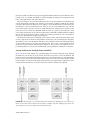
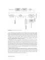
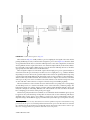
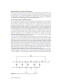
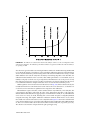
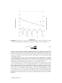
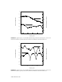
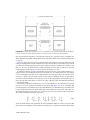
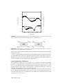
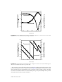
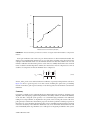
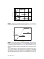
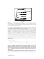
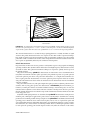
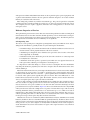
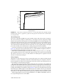
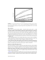
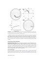
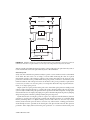
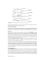
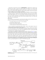
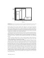
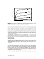
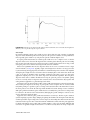
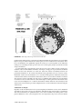
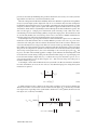
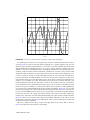
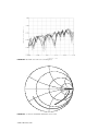
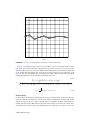
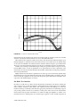
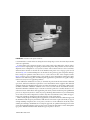
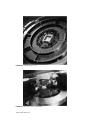
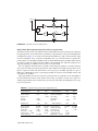
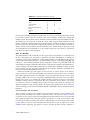
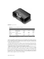
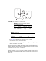
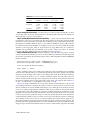
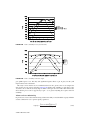
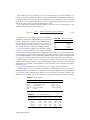
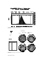
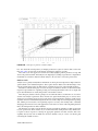
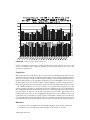

![ダウンロード[ 4.861MB]](http://vs1.manualzilla.com/store/data/006616823_2-ed416674831b1976fcbdc9201a78fe85-150x150.png)