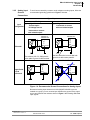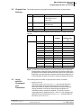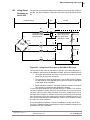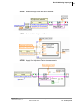
1
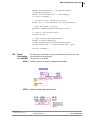
DNA/DNR-AI-208 Strain Gauge Analog Input Layer — User Manual 18-bit, 8-channel, 4- and 6-wire Strain Gauge Differential Input Layers for the PowerDNA Cube and RACKtangle chassis November 2013 Version 4.6 PN Man-DNx-AI-208-1113 © Copyright 1998-2010 United Electronic Industries, Inc. All rights reserved. i No part of this publication may be reproduced, stored in a retrieval system, or transmitted, in any form by any means, electronic, mechanical, by photocopying, recording, or otherwise without prior written permission. Information furnished in this manual is believed to be accurate and reliable. However, no responsibility is assumed for its use, or for any infringements of patents or other rights of third parties that may result from its use. All product names listed are trademarks or trade names of their respective companies. See UEI’s website for complete terms and conditions of sale: http://www.ueidaq.com/company/terms.aspx Contacting United Electronic Industries: Mailing Address: 27 Renmar Avenue Walpole, MA 02081 U.S.A. For a list of our distributors and partners in the US and around the world, please see http://www.ueidaq.com/partners/ Support: Telephone: Fax: (508) 921-4600 (508) 668-2350 Also see the FAQs and online “Live Help” feature on our web site. Internet Support: Support [email protected] Web-Site www.ueidaq.com FTP Site ftp://ftp.ueidaq.com Product Disclaimer: WARNING! DO NOT USE PRODUCTS SOLD BY UNITED ELECTRONIC INDUSTRIES, INC. AS CRITICAL COMPONENTS IN LIFE SUPPORT DEVICES OR SYSTEMS. Products sold by United Electronic Industries, Inc. are not authorized for use as critical components in life support devices or systems. A critical component is any component of a life support device or system whose failure to perform can be reasonably expected to cause the failure of the life support device or system, or to affect its safety or effectiveness. Any attempt to purchase any United Electronic Industries, Inc. product for that purpose is null and void and United Electronic Industries Inc. accepts no liability whatsoever in contract, tort, or otherwise whether or not resulting from our or our employees' negligence or failure to detect an improper purchase. NOTE: Specifications shown in this document may change from time to time. Check with UEI for current status. ii iii Table of Contents Chapter 1 Introduction .................................................... 1 1.1 Organization . . . . . . . . . . . . . . . . . . . . . . . . . . . . . . . . . . . . . . . . . . . . . . . . . . . . . . . . 1 1.2 The DNx-AI-208 Analog Input Layer. . . . . . . . . . . . . . . . . . . . . . . . . . . . . . . . . . . . . . 3 1.3 Device Architecture. . . . . . . . . . . . . . . . . . . . . . . . . . . . . . . . . . . . . . . . . . . . . . . . . . . 4 1.4 1.4.1 1.4.2 Layer Connectors and Wiring . . . . . . . . . . . . . . . . . . . . . . . . . . . . . . . . . . . . . . . . . . . 4 Connectors. . . . . . . . . . . . . . . . . . . . . . . . . . . . . . . . . . . . . . . . . . . . . . . . . . . . 5 Analog Input Ground Connections. . . . . . . . . . . . . . . . . . . . . . . . . . . . . . . . . . 6 Chapter 2 Programming with the High Level API . . . . . . . . . . . . . . . . . . . . . . . . . . . . . . . 7 2.1 Creating a session . . . . . . . . . . . . . . . . . . . . . . . . . . . . . . . . . . . . . . . . . . . . . . . . . . . 7 2.2 Configuring Channels and Excitation. . . . . . . . . . . . . . . . . . . . . . . . . . . . . . . . . . . . . 7 2.3 Configuring the Timing . . . . . . . . . . . . . . . . . . . . . . . . . . . . . . . . . . . . . . . . . . . . . . . . 8 2.4 Reading Data . . . . . . . . . . . . . . . . . . . . . . . . . . . . . . . . . . . . . . . . . . . . . . . . . . . . . . . 8 2.5 Cleaning-up the Session. . . . . . . . . . . . . . . . . . . . . . . . . . . . . . . . . . . . . . . . . . . . . . . 8 Chapter 3 Programming with the Low-Level API . . . . . . . . . . . . . . . . . . . . . . . . . . . . . . . 9 3.1 Configuration Settings. . . . . . . . . . . . . . . . . . . . . . . . . . . . . . . . . . . . . . . . . . . . . . . . . 9 3.2 Channel List Settings . . . . . . . . . . . . . . . . . . . . . . . . . . . . . . . . . . . . . . . . . . . . . . . . 10 3.3 Layer-specific Commands and Parameters . . . . . . . . . . . . . . . . . . . . . . . . . . . . . . . 11 3.4 Using Layer in ACB Mode. . . . . . . . . . . . . . . . . . . . . . . . . . . . . . . . . . . . . . . . . . . . . 14 3.5 Using Layer in DMap mode . . . . . . . . . . . . . . . . . . . . . . . . . . . . . . . . . . . . . . . . . . . 16 Appendix A – Accessories . . . . . . . . . . . . . . . . . . . . . . . . . . . . . . . . . . . . . . . . . . . . . . . . . 18 A.1 DNA-STP-AI-208 Screw Terminal Panel . . . . . . . . . . . . . . . . . . . . . . . . . . . . . . . . . 18 A.2 Other Accessories. . . . . . . . . . . . . . . . . . . . . . . . . . . . . . . . . . . . . . . . . . . . . . . . . . . 24 A.3 Layer Calibration. . . . . . . . . . . . . . . . . . . . . . . . . . . . . . . . . . . . . . . . . . . . . . . . . . . . 24 Appendix B – Shunt Calibration . . . . . . . . . . . . . . . . . . . . . . . . . . . . . . . . . . . . . . . . . . . . . 25 B.1 Introduction . . . . . . . . . . . . . . . . . . . . . . . . . . . . . . . . . . . . . . . . . . . . . . . . . . . . . . . . 25 B.2 Theory. . . . . . . . . . . . . . . . . . . . . . . . . . . . . . . . . . . . . . . . . . . . . . . . . . . . . . . . . . . . 25 B.3 Using Shunt Resistors on the AI-208 . . . . . . . . . . . . . . . . . . . . . . . . . . . . . . . . . . . . 28 B.4 Configuring Framework for Shunt Calibration . . . . . . . . . . . . . . . . . . . . . . . . . . . . . 29 B.5 Shunt Calibration in C++. . . . . . . . . . . . . . . . . . . . . . . . . . . . . . . . . . . . . . . . . . . . . . 30 B.6 Shunt Calibration in LabVIEW . . . . . . . . . . . . . . . . . . . . . . . . . . . . . . . . . . . . . . . . . 31 Index . . . . . . . . . . . . . . . . . . . . . . . . . . . . . . . . . . . . . . . . . . . . . . . . . . . . . . . . . . . . . . . . . 33 © Copyright 2009 United Electronic Industries, Inc. Tel::508-921-4600 Date: August 2009 www.ueidaq.com Vers: 1.8 AI-208TOC.fm List of Figures Chapter 1 — Introduction . . . . . . . . . . . . . . . . . . . . . . . . . . . . . . . . . . . . . . . . . . . . . . . . . . . . 1 1-1 Photos of DNR and DNA-AI-208 Boards ....................................................................... 4 1-2 Block Diagram of DNx-AI-208 Device Architecture........................................................ 4 1-3 DB-37 I/O Connector Pinout .......................................................................................... 5 1-4 Recommended Ground Connections for Analog Inputs ................................................ 6 Chapter 2 — Programming with the High Level API. . . . . . . . . . . . . . . . . . . . . . . . . . . . . . . 7 (None) Chapter 3 — Programming with the Low-Level API . . . . . . . . . . . . . . . . . . . . . . . . . . . . . . . 9 (None) Appendix A – Accessories . . . . . . . . . . . . . . . . . . . . . . . . . . . . . . . . . . . . . . . . . . . . . . . . . . 18 A-1 Photo of DNA-STP-AI-208 Screw Terminal Panel....................................................... 18 A-2 Pinout Diagram for the DNA-STP-AI-208 .................................................................... 20 A-3 Single-Channel Wiring Diagram — Full-Bridge............................................................ 20 A-4 Single-Channel Wiring Diagram — Half-Bridge ........................................................... 21 A-5 Single-Channel Wiring Diagram — Quarter-Bridge .................................................... 22 A-6 Physical Layout of STP-AI-208 Board ......................................................................... 23 Appendix B – Shunt Calibration . . . . . . . . . . . . . . . . . . . . . . . . . . . . . . . . . . . . . . . . . . . . . . 25 B-1 Strain Gauge Bridge .................................................................................................... 25 B-2 Strain Gauge with Shunt Resistance Rs Added .......................................................... 26 B-3 Using Shunt Resistors on the DNA-AI-208 Layer ........................................................ 28 © Copyright 2009 United Electronic Industries, Inc. Tel::508-921-4600 Date: November 2010 www.ueidaq.com Vers: 1.9 AI-208LOF.fm DNx-AI-208 Analog Input Layer Chapter 1 Introduction Chapter 1 Introduction This document outlines the feature set and use of the DNA/DNR-AI-208 strain gauge analog input layer(s). The DNA version is used with the PowerDNA Core Module, the DNR with the rack-mounted UeiDaq RACKtangle chassis This manual describes the following products: • DNA/DNR-AI-208, 18-bit, 8-channel, differential input, analog input strain gauge layer board(s) • DNA-STP-AI-208 Screw Terminal Panel Accessory Board, designed as a convenient interface for connecting full-, half, and quarter-bridge strain gauge-type sensors to the DNA/DNR-AI-208 board. • Accessory modules such as cables. The DNR version is identical to the DNA version except that the DNR version is designed to plug into a RACKtangle backplane instead of a Cube. 1.1 Organization This DNA/DNR-AI-208 User Manual is organized as follows: • Introduction This chapter provides an overview of DNA/DNR-AI-208 board/layer features, accessories, and what you need to get started. • DNx-AI-208 Layer This chapter provides an overview of the device architecture, connectivity, logic, and accessories for the DNA/DNR-AI-208 layer board. • Programming with High-Level API This chapter provides a general overview of procedures that show how to create a session, configure the session, and generate output on a DNA/DNR-AI-208 layer, working with the UeiDaq Framework HighLevel API. • Programming with the Low-Level API This chapter describes the Low-Level API commands for configuring and using a DNA/DNR-AI-208 layer. • Appendices: A--Accessories This appendix provides a list of accessories available for use with a DNA/DNR-AI-208 layer. B--Shunt Calibration Support in Framework This appendix describes procedures for using Framework to perform shunt calibration of strain gauges. It includes examples of C++ code and LabVIEW procedures for shunt calibration. • Index This is an alphabetical index of topics covered in this manual. NOTE: A glossary of terms used with the PowerDNA Cube and layers can be viewed and/or downloaded from www.ueidaq.com © Copyright 2009 United Electronic Industries, Inc. Tel: 508-921-4600 www.ueidaq.com Date: November 2013 Vers: 4.6 File: AI208 Chap1.fm 1 DNx-AI-208 Analog Input Layer Chapter 1 Introduction Manual Conventions To help you get the most out of this manual and our products, please note that we use the following conventions: Tips are designed to highlight quick ways to get the job done, or reveal good ideas you might not discover on your own. NOTE: Notes alert you to important information. CAUTION! Caution advises you of precautions to take to avoid injury, data loss, and damage to your boards or a system crash. Text formatted in bold typeface generally represents text that should be entered verbatim. For instance, it can represent a command, as in the following example: “You can instruct users how to run setup using a command such as setup.exe.” © Copyright 2009 United Electronic Industries, Inc. Tel: 508-921-4600 www.ueidaq.com Date: November 2013 Vers: 4.6 File: AI208 Chap1.fm 2 DNx-AI-208 Analog Input Layer Chapter 1 Introduction 1.2 The DNx-AI-208 Analog Input Layer This manual describes the DNA-AI-208 18-bit, 8-channel, Strain Gauge Analog Input Board/Layer. It also describes the DNA-STP-208 Screw Terminal Panel accessory board. The technical specifications for the DNA/DNR-AI-208 Analog Input Layer are listed in Table 1-1. Number of channels ADC resolution Sampling rate Input range FIFO size Wiring scheme Bridge configurations Bridge resistance Input impedance Gains Gain accuracy Offset accuracy Temperature drift Offset drift Gain drift Shunt calibration Isolation Overvoltage protection Excitation voltage Excitation current Excitation type Power consumption Operating temp. (tested) Operating humidity 8 (differential) 18 bits 1 S/s - 1 kS/s per channel ±10V 512 samples 4- and 6-wire (with Kelvin connection); all channels share the same ground Full-Bridge Half-Bridge (with ext. terminal panel) Quarter-Bridge (with ext. terminal panel) 120Ω, 350Ω, 1000Ω, and custom 10MΩ in parallel with 50pF 1,2,4,8,10,20,40,80,100,200,400,800 See Table 1-2. 5μV/°C typ 30ppm/C° @ G=1, 45ppm/C° @ G=800 Onboard (software selectable) - 256 steps fom 5K to 205K; External 350 Vrms -40V..+55V 1.5V - 10.05V (software selectable) 85 mA, per channel Pulsing (for overheating protection) bridge resistance/excitation dependent; 2.5W - 4.5W -40°C to +85°C 90%, non-condensing Table 1-1. DNx-AI-208 Technical Specifications Gain 1 2 4 8 10 20 40 80 100 200 400 800 ±LSB 2 2 4 4 4 4 6 6 6 6 10 18 ±% 0.000763 0.000763 0.001526 0.001526 0.001526 0.001526 0.002289 0.002289 0.002289 0.002289 0.003815 0.006866 mV 0.152588 0.076294 0.076294 0.038147 0.030518 0.015259 0.011444 0.005722 0.004578 0.002289 0.001907 0.001717 Table 1-2. Offset and Gain Calibration Limits © Copyright 2009 United Electronic Industries, Inc. Tel: 508-921-4600 www.ueidaq.com Date: November 2013 Vers: 4.6 File: AI208 Chap1.fm 3 DNx-AI-208 Analog Input Layer Chapter 1 Introduction Figure 1-1 is a photo of the DNA and DNR-AI-208 Layer boards. 120-pin DNR bus connector 120-pin DNA bus connector Layer Position Jumpers DB-37 (female) 37-pin I/O connectors Figure 1-1. Photos of DNR and DNA-AI-208 Boards 1.3 Device The DNA/DNR-AI-208 Analog Input Layer board has eight individual analog Architecture input channels. A Block Diagram of the board/layer is shown in Figure 1-2. Figure 1-2 Block Diagram of DNx-AI-208 Device Architecture 1.4 Layer Connectors and Wiring © Copyright 2009 United Electronic Industries, Inc. Two D/A converters produce excitation voltages. The first converter drives excitation on even numbered channels, and the second one to odd numbered channels. Excitation voltage can be switched on and off on a per-channel basis. When an AI-208 performs continuous acquisition, it applies voltage to the next channel in the channel list while acquiring the current channel. This technique gives a channel enough time to settle and limits current consumption and heat dissipation by the layer. Tel: 508-921-4600 www.ueidaq.com Date: November 2013 Vers: 4.6 File: AI208 Chap1.fm 4 DNx-AI-208 Analog Input Layer Chapter 1 Introduction The AI-208 layer can measure voltage on every channel between the S- and S+ terminals (differential mode, channels 0-7), between the Px+ lines (channels 0x10-0x17) and signal ground, and between the PSx+ and signal ground (channels (0x20-0x27). The AI-208 layer can also be used to measure signals from differential signal sources other than bridges, using the S+ and S- terminals. In such application situations, sensor excitation is usually not required. Precise measurement is achieved through the use of more than 8 channels internally in the AI-208 board. NOTE: For descriptions of connections used with quarter-, half-, and full-bridge circuits, refer to Figure A-3, Figure A-4, and Figure A-5 in the Appendix. 1.4.1 Connectors The pinout of the 37-pin connector for the DNA/DNR-AI-208 Layer board is shown in Figure 1-3. A physical layout of the board is shown in Figure 1-3. External Trigger (Input only) Figure 1-3. DB-37 I/O Connector Pinout When using a long cable to a sensor, be sure to use the same gauge wire for the excitation source, GND, and GND Sense lines. © Copyright 2009 United Electronic Industries, Inc. Tel: 508-921-4600 www.ueidaq.com Date: November 2013 Vers: 4.6 File: AI208 Chap1.fm 5 DNx-AI-208 Analog Input Layer Chapter 1 Introduction 1.4.2 Analog Input Ground Connections To avoid errors caused by common mode voltages on analog inputs, follow the recommended grounding guidelines in Figure 1-4 below. Type of Input Floating Typical Signal Sources: Instruments or sensors with non-isolated outputs DNA-STP-37, DNA-STP-AI-U Sig + Vin _ Differential DNA-STP-AI-U Ret Sig + Vin _ Ret AGnd Two resistors (10k <R< 100k) provide return paths to ground for bias currents. AInX Typical Signal Sources: Thermocouples DC Voltage Sources Instruments or sensors with isolated outputs AInX Input Configuration Grounded AGnd Add this connection to ensure that both grounds are at the same potential. NOT RECOMMENDED DNA-STP-AI-U _ + Ret _ Sig Vin AGnd AInX Vin AInX Single-Ended, Ground Referenced DNA-STP-AI-U Sig + Ret AGnd Figure 1-4. Recommended Ground Connections for Analog Inputs Because all analog input channels in AI-201/202/207/208/225 layers are isolated as a group, you can connect layer AGND to the ground of the signal source and eliminate the resistors shown in Figure 1-4 for floating differential input signals. © Copyright 2009 United Electronic Industries, Inc. Tel: 508-921-4600 www.ueidaq.com Date: November 2013 Vers: 4.6 File: AI208 Chap1.fm 6 DNx-AI-208 Analog Input Layer Chapter 2 Programming with the High Level API Chapter 2 Programming with the High Level API This chapter describes how to program the PowerDNA/DNR-AI-208 using UeiDaq’s Framework High Level API. Since Framework is object oriented; its objects can be manipulated in the same manner using different development environments, such as Visual C++, Visual Basic, or LabVIEW. Although the following section focuses only on the C++ API, the concept is the same no matter what programming language you use. Please refer to the “UeiDaq Framework User Manual” for more information on using other programming languages. 2.1 Creating a session The Session object controls all operations on your PowerDNA device. Therefore, the first task is to create a session object, as follows. CUeiSession session; 2.2 Configuring Channels and Excitation Framework uses resource strings to select each device, subsystem and channels to use within a session. The resource string syntax is similar to a web URL: <device class>://<IP address>/<Device Id>/<Subsystem><Channel list> For PowerDNA, the device class is pdna. For example, the following resource string selects analog input channels 0,2,3,4 on device 1 at IP address 192.168.100.2: “pdna://192.168.100.2/Dev1/Ai0,2,3,4” The gain to be applied on each channel is specified with low and high input limits. For example, the AI-208 available gains are 1, 2, 4, 8, 10, 20, 40, 80,100, 200, 400, 800 and the maximum input range is [-10V, 10V]. To select a gain of 100, you must specify input limits of [-0.1V, 0.1V]. // Configure channels 0,1 to use a gain of 100 in // differential mode session.CreateAIChannel(“pdna://192.168.100.2/Dev0/Ai0,1”, -0.1, 0.1, UeiAIChannelInputModeDifferential); To program the excitation circuitry, you need to configure the channel list using the session object method “CreateAIVExChannel” instead of “Cre- ateAIChannel”. This method also gives you the ability to select the bridge configuration you want and to select whether or not you wish to obtain the acquired data already scaled in mV/V (acquired voltage divided by actual excitation voltage), as follows: © Copyright 2009 United Electronic Industries, Inc. Tel: 508-921-4600 www.ueidaq.com Date: November 2013 Vers: 4.6 File: AI208 Chap2.fm 7 DNx-AI-208 Analog Input Layer Chapter 2 Programming with the High Level API // Configure channels 0,1 to use a gain of 100 in // differential mode, program the excitation to 10V and // turn on scaling with excitation session.CreateAIExChannel(“pdna://192.168.100.2/Dev0/Ai0,1”, -0.1, 0.1, UeiSensorFullBridge, 10.0, true, UeiAIChannelInputModeDifferential); 2.3 Configuring the Timing You can configure the AI-208 to run in simple mode (point by point) or buffered mode (ACB mode). In simple mode, the delay between samples is determined by software on the host computer. In buffered mode, the delay between samples is determined by the AI-208 onboard clock. The following sample shows how to configure the simple mode. Please refer to the “UeiDaq Framework User’s Manual” to learn how to use the other timing modes. session.ConfigureTimingForSimpleIO(); 2.4 Reading Data Reading data from the AI-208 is done using a reader object. There is a reader object to read raw data coming straight from the A/D converter. There is also a reader object to read data already scaled to volts or mV/V. The following sample code shows how to create a scaled reader object and read samples. // Create a reader and link it to the session’s stream CUeiAnalogScaledReader reader(session.GetDataStream()); // read one scan, the buffer must be big enough to contain // one value per channel double data[2]; reader.ReadSingleScan(data); 2.5 Cleaning-up the Session The session object will clean itself up when it goes out of scope or when it is destroyed. However, you can also clean up the session manually (to reuse the object with a different set of channels or parameters). session.CleanUp(); © Copyright 2009 United Electronic Industries, Inc. Tel: 508-921-4600 www.ueidaq.com Date: November 2013 Vers: 4.6 File: AI208 Chap2.fm 8 DNx-AI-208 Analog Input Layer Chapter 3 Programming with the Low-Level API Chapter 3 Programming with the Low-Level API This section describes how to program the PowerDNA cube using the Low-level API The low-level API offers direct access to PowerDNA DAQBios protocol and also allows you to access device registers directly. We recommend that, when possible, you use the UeiDaq Framework High-Level API (see Chapter 2), because it is easier to use. You should need to use the low-level API only if you are using an operating system other than Windows. 3.1 Configuration Configuration settings are passed through the DqCmdSetCfg() and DqAcbInitOps() functions. Settings Not all configuration bits apply to the AI-208 layer. The following bits are used: #define DQ_LN_IRQEN (1L<<10) #define DQ_LN_PTRIGEDGE1 (1L<<9) #define DQ_LN_PTRIGEDGE0 (1L<<8) software, #define DQ_LN_STRIGEDGE1 (1L<<7) #define DQ_LN_STRIGEDGE0 (1L<<6) software, 01 - rising, #define DQ_LN_CLCKSRC1 #define DQ_LN_CLCKSRC0 HW, 11 -EXT #define DQ_LN_ACTIVE #define DQ_LN_ENABLED // enable layer irqs // stop trigger edge MSB // stop trigger edge: 00 // 01 - rising, 02 - falling // start trigger edge MSB // start trigger edge: 00 - (1L<<3) (1L<<2) // 02 - falling // CL clock source MSB // CL clock source 01 - SW, 10 - (1L<<1) (1L<<0) // "STS" LED status // enable operations For streaming operations with hardware clocking, the user has to select the following flags: DQ_LN_ENABLE | DQ_LN_CLCKSRC0 | DQ_LN_STREAMING | DQ_LN_IRQEN | DQ_LN_ACTIVE DQ_LN_ENABLE enables all layer operations. DQ_LN_CLCKSRC0 selects the internal channel list clock (CL) source as a time base. The AI-208 layer supports the CL clock only where the time between consecutive channel readings is calculated by the rule of maximizing setup time per channel. If you’d like to select the CL clock from an external clock source such as the SYNCx line, set DQ_LN_CLCKSRC1 as well. Aggregate rate = Per-channel rate * Number of channels © Copyright 2009 United Electronic Industries, Inc. Tel: 508-921-4600 www.ueidaq.com Date: November 2013 Vers: 4.6 File: AI208 Chap3.fm 9 DNx-AI-208 Analog Input Layer Chapter 3 Programming with the Low-Level API 3.2 Channel List The AI-208 layer has a very simple channel list structure, as shown below: Settings Bit Name Purpose Macro 31 DQ_LNCL_NEXT Tells firmware that there is a “Next Entry” in the channel list 20 DQ_LNCL_TSRQ Request timestamp as the next data point 11..8 Gain DQ_LNCL_GAIN() 7..0 Channel number Gains are different for different options of the AI-208 layer, as listed in the following table. Layer type Range Gain Gain Number Min. Allowed Settling Time, us AI-201-208 ±10V 1 0 40 ±5V 2 1 50 ±2.5V 4 2 60 ±1.25V 8 3 70 ±1V 10 4 80 ±500mV 20 5 100 ±250mV 40 6 120 ±125mV 80 7 140 ±100mV 100 8 160 ±50mV 200 9 180 ±25mV 400 10 200 ±12.5mV 800 11 220 NOTE: The Minimum Allowed Settling Time is the shortest time for which the firmware allows a channel to settle. When the scan rate and channel are programmed, the firmware allocates the minimum time for each channel depending on the gain selected, and then stretches the settling time as much as possible to utilize at least 2/3 of the time between scan clocks. 3.3 Layerspecific Commands and Parameters © Copyright 2009 United Electronic Industries, Inc. The AI-208 layer has a number of layer-specific functions, as follows. • DqAdv208Read This function uses DqReadAIChannel() but converts data using internal knowledge of the input range and gain of every channel. When this function is called for the first time, the firmware stops any ongoing operation on the device specified and reprograms it in accordance with the channel list supplied. This function uses the preprogrammed CL update frequency – 10Hz. You can reprogram the update frequency by calling the DqCmdSetClk() command after the first call to DqAdv208Read(). Tel: 508-921-4600 www.ueidaq.com Date: November 2013 Vers: 4.6 File: AI208 Chap3.fm 10 DNx-AI-208 Analog Input Layer Chapter 3 Programming with the Low-Level API Therefore, you cannot call this function when the layer is involved in any streaming or data mapping operations. If you specify a short timeout delay, this function can time out when called for the first time because it is executed as a pending command, and layer programming takes up to 10ms. Once this function is called, the layer continuously acquires data and every “next call” function returns the latest acquired data If you would like to cancel ongoing sampling, call the same function with 0xFFFFFFFF as a channel number. • DqAdv208SetControl This function allows you to set up different internal parameters. The following sub-functions are available: DQL_IOCTL208_SET_Ra: set value for shunt calibration resistor A in 256 steps (P+ to S+) DQL_IOCTL208_SET_Rb: set value for shunt calibration resistor B in 256 steps (S+ to P-). DQL_IOCTL208_SET_EXC_A: set excitation DAC A. DQL_IOCTL208_SET_EXC_B: set excitation DAC B. DQL_IOCTL208_SET_EXC_CH: switch excitation channels on or off. • DqAdv208SetExcVoltage Set excitation voltage for excitation sources A and B and measure it back using specified channels. The AI-208 layer is capable of providing two sources of excitation voltage — Excitation A is connected to even channels and B is connected to odd channels. Excitation voltage can be selected and set at any level from 1.5V to 10V. This function sets up excitation voltage as close as possible to the requested level and reads it back from the selected channels. The user can select either channels 0x10 through 0x17 to read the excitation voltage from the Px+ terminal (four-wire connection), or channels 0x20 through 0x27 to read the excitation voltage from PSx+ terminals (six-wire connection). All readings are performed relative to AGND. The user has to use the read-back excitation voltage from the terminal because of DACs; there is a voltage drop in the strain gauge leads and DAQ output quantization error amounts to 1/1024 of the range. Note that this function must be called before starting data acquisition or reading channels in order to set up the proper excitation voltage source before gathering data. • DqAdv208ReadChannel This function performs “raw” measurements of the following values: 0x0 .0x27: DQL_IOCTL208_READ_AGND: connect both differential inputs of the PGA to analog ground. DQL_IOCTL208_READ_REF: read 2.5V voltage reference DQL_IOCTL208_READ_Rs: measure switch resistance Rs DQL_IOCTL208_READ_Rx: measure multiplexer resistance DQL_IOCTL208_READ_Ra: measure shunt resistor Ra DQL_IOCTL208_READ_Rb: measure shunt resistor Rb DQL_IOCTL208_READ_SS: measure S+ to SDQL_IOCTL208_READ_PP: measure P+ to AGND DQL_IOCTL208_READ_PS: measure PS+ to AGND © Copyright 2009 United Electronic Industries, Inc. Tel: 508-921-4600 www.ueidaq.com Date: November 2013 Vers: 4.6 File: AI208 Chap3.fm 11 DNx-AI-208 Analog Input Layer Chapter 3 Programming with the Low-Level API Because the resistance can differ from channel to channel (current is flowing through different channels of the same multiplexer which can have different resistances), you should set up the channel number to be used. This function returns the number of samples requested for averaging. Data is returned in raw format. • DqAdv208MeasureParams This function is used to measure a variety of AI-208 front-end parameters (see channel equivalent diagram): VrefReference voltage, Volts VexcExcitation voltage, Volts VsVmeas for Rs, Volts RsSwitch resistance, Ohms VxVmeas for Rx, Volts RxMux resistance, Ohms VaVmeas for Ra, Volts RaResistance of shunt resistor Ra (plus 5k constant!), Ohms VbVmeas for Rb, Volts RbResistance of shunt resistor Rb (plus 5k constant!), Ohms Before the function can measure these parameters, specify the measurement conditions: ChannelChannel being used for measurements ExcAExcitation level A (even channels, 16 bit) ExcBExcitation level B (odd channels, 16 bit) RaShunt A level (8 bit, 256 positions from 0 to 200k) RbShunt B level (8 bit, 256 positions from 0 to 200k) The AI-208 layer has a 14-bit excitation DAC and an 8-bit shunt calibration digital potentiometer. The digital potentiometer has a ±30% initial resistance accuracy, 60-150 Ohm runner resistance, and a 35ppm temperature coefficient. Thus, measuring this resistor is crucial for shunt calibration. An additional series resistor (4.99k 0.01%) is inserted in the shunt calibration circuit to ensure precise measurement. 3.4 Using Layer in ACB Mode This is a pseudo-code example that highlights the sequence of functions needed to use ACB on the AI-208 layer. A complete example with error checking can be found in the directory SampleACB208. #include "PDNA.h" // unit configuration word #define CFG208 (DQ_LN_ENABLED \ |DQ_LN_ACTIVE \ |DQ_LN_CLCKSRC0 \ |DQ_LN_RAW32) uint32 Config = CFG208; STEP 1: Start DQE engine. #ifndef _WIN32 DqInitDAQLib(); #endif © Copyright 2009 United Electronic Industries, Inc. Tel: 508-921-4600 www.ueidaq.com Date: November 2013 Vers: 4.6 File: AI208 Chap3.fm 12 DNx-AI-208 Analog Input Layer Chapter 3 Programming with the Low-Level API // Start engine DqStartDQEngine(1000*1, &pDqe, NULL); // Open communication with IOM hd0 = DqOpenIOM(IOM_IPADDR0, DQ_UDP_DAQ_PORT, TIMEOUT_DELAY, &RdCfg); // Receive IOM crucial identification data DqCmdEcho(hd0, DQRdCfg); // Set up channel list for (n = 0; n < CHANNELS; n++) { CL[n] = n; } STEP 2: Create and initialize host and IOM sides. // Now we are going to test device DqAcbCreate(pDqe, hd0, DEVN, DQ_SS0IN, &bcb); // Let’s assume that we are dealing with AI-208 device dquser_initialize_acb_structure(); // Now call the function DqAcbInitOps(bcb, &Config, 0, //TrigSize, NULL, //pDQSETTRIG TrigMode, &fCLClk, 0, //float* fCVClk, &CLSize, CL, 0, //uint32* ScanBlock, &acb); printf("Actual clock rate: %f\n", fCLClk); // Now set up events DqeSetEvent(bcb, DQ_eFrameDone|DQ_ePacketLost|DQ_eBufferError|DQ_ePacketOOB); STEP 3: Start operation. // Start operations DqeEnable(TRUE, &bcb, 1, FALSE); STEP 4: Process data. // We will not use event notification at first - just retrieve scans while (keep_looping) { DqeWaitForEvent(&bcb, 1, FALSE, EVENT_TIMEOUT, &events); if (events & DQ_eFrameDone) { minrq = acb.framesize; © Copyright 2009 United Electronic Industries, Inc. Tel: 508-921-4600 www.ueidaq.com Date: November 2013 Vers: 4.6 File: AI208 Chap3.fm 13 DNx-AI-208 Analog Input Layer Chapter 3 Programming with the Low-Level API avail = minrq; while (TRUE) { DqAcbGetScansCopy(bcb, data, acb.framesize, acb.framesize, &size, &avail); samples += size*CHANNELS; for (i = 0; i < size * CHANNELS; i++) { fprintf(fo, "%f\t", *((float*)data + i)); if ((i % CHANNELS) == (CHANNELS - 1)) { fprintf(fo, "\n"); } } printf("eFD:%d scans received (%d samples) min=%d avail=%d\n", size, samples, minrq, avail); if (avail < minrq) { break; } } } } STEP 5: Stop operation. DqeEnable(FALSE, &bcb, 1, FALSE); STEP 6: Clean up. DqAcbDestroy(bcb); DqStopDQEngine(pDqe); DqCloseIOM(hd0); #ifndef _WIN32 DqCleanUpDAQLib(); #endif 3.5 Using Layer in DMap mode #include "PDNA.h" STEP 1: Start DQE engine. #ifndef _WIN32 DqInitDAQLib(); #endif // Start engine DqStartDQEngine(1000*10, &pDqe, NULL); // open communication with IOM hd0 = DqOpenIOM(IOM_IPADDR0, DQ_UDP_DAQ_PORT, TIMEOUT_DELAY, &DQRdCfg); // Receive IOM crucial identification data DqCmdEcho(hd0, DQRdCfg); © Copyright 2009 United Electronic Industries, Inc. Tel: 508-921-4600 www.ueidaq.com Date: November 2013 Vers: 4.6 File: AI208 Chap3.fm 14 DNx-AI-208 Analog Input Layer Chapter 3 Programming with the Low-Level API for (i = 0; i < DQ_MAXDEVN; i++) { if (DQRdCfg->devmod[i]) { printf("Model: %x Option: %x\n", DQRdCfg->devmod[i], DQRdCfg->option[i]); } else { break; } } STEP 2: Create and initialize host and IOM sides. DqDmapCreate(pDqe, hd0, &pBcb, UPDATE_PERIOD, &dmapin, &dmapout); STEP 3: Add channels into DMap. for (i = 0; i < CHANNELS; i++) { DqDmapSetEntry(pBcb, DEVN, DQ_SS0IN, i, DQ_ACB_DATA_RAW, 1, &ioffset[i]); } DqDmapInitOps(pBcb); DqeSetEvent(pBcb, DQ_eDataAvailable|DQ_ePacketLost|DQ_eBufferError|DQ_ePacketOOB); STEP 4: Start operation. DqeEnable(TRUE, &pBcb, 1, FALSE); STEP 5: Process data. while (keep_looping) { DqeWaitForEvent(&pBcb, 1, FALSE, timeout, &eventsin); if (eventsin & DQ_eDataAvailable) { datarcv++; printf("\ndata "); for (i = 0; i < CHANNELS; i++) { printf("%04x ", *(uint32*)ioffset[i]); } } } STEP 6: Stop operation. DqeEnable(FALSE, &pBcb, 1, FALSE); STEP 7: Clean up. DqDmapDestroy(pBcb); DqStopDQEngine(pDqe); DqCloseIOM(hd0); #ifndef _WIN32 DqCleanUpDAQLib(); #endif © Copyright 2009 United Electronic Industries, Inc. Tel: 508-921-4600 www.ueidaq.com Date: November 2013 Vers: 4.6 File: AI208 Chap3.fm 15 DNx-AI-208 Analog Input Layer Chapter 3 Programming with the Low-Level API © Copyright 2009 United Electronic Industries, Inc. Tel: 508-921-4600 www.ueidaq.com Date: November 2013 Vers: 4.6 File: AI208 Chap3.fm 16 DNx-AI-208 Analog Input Layer 17 Appendix A Accessories A.1 DNA-STP-AI208 Screw Terminal Panel The DNA-STP-AI-208 Screw Terminal Panel is an easy-to-use, versatile, accessory for direct connection of strain gauge and other bridge-type sensors to the DNA-AI-208 Strain Gauge Analog Input Layer board. It can accept signals from 8 strain gauge-type sensor channels in several types of bridge configurations — full-bridge (4- and 6-wire circuits), half-bridge (3- and 4-wire circuits), and quarter-bridge (2- and 3-wire circuits) configurations. Note that quarter- and halfbridge configurations require user-populated bridge completion resistors. Since the panel is supplied with a DB-37 board-mounted connector that mates directly with the I/O connector on a DNA-AI-208 Layer board, it can be plugged directly into the Layer in the Cube. As an alternative, you can use a DNA-CBL-37 37-way Flat Ribbon Cable or a DNA-CBL-37S 37-way Round Cable to mount the unit as a desktop panel. A photo of the panel is shown in Figure A-1 below. Figure A-1 Photo of DNA-STP-AI-208 Screw Terminal Panel © Copyright 2009 United Electronic Industries, Inc. Tel: 508-921-4600 www.ueidaq.com Date: November 2013 Vers: 4.6 File: AI-208 App A.fm DNx-AI-208 Analog Input Layer 18 The Technical Specifications for the DNA-STP-AI-208 are listed in the table below. Technical Specifications: Number of channels 8 Bridge Configurations Full-Bridge; Half-Bridge; Quarter-Bridge Wiring Schemes: Full-Bridge Half-Bridge Quarter-Bridge 6- and 4-wire; 4- and 3-wire; 3- and 2-wire Operating temperature -20°C to 85°C Operating humidity 90%, non-condensing Dimensions 4 x 2.5 x 0.7” The Wiring Settings for the DNA-STP-AI-208 panel are listed in the table below. Bridge Configuration Wiring Scheme 6-wire Full-Bridge 4-wire 4-wire Half-Bridge 3-wire 3-wire Quarter-Bridge 2-wire Jumper Settings J=Off J=On J=Off J=On J=Off J=On Bridge-Completion Resistors None required RA = RB or RN RA = RB or RN; RC = RSTRAIN The Bridge Completion Resistors in the table are shown in the bridge circuit wiring diagrams illustrated in Figure A-4 and Figure A-5. © Copyright 2009 United Electronic Industries, Inc. Tel: 508-921-4600 www.ueidaq.com Date: November 2013 Vers: 4.6 File: AI-208 App A.fm DNx-AI-208 Analog Input Layer 19 The Pinout for the DNA-STP-AI-208 DB-37connector is as follows. g DB-37 (male) 37-pin connector: S7P7+ AGND S6+ PS6+ S5+ PS5+ S4P4+ S3P3+ AGND S2+ PS2+ S1+ PS1+ S0P0+ 20 21 22 23 24 25 26 27 28 29 30 31 32 33 34 35 36 37 1 2 3 4 5 6 7 8 9 10 11 12 13 14 15 16 17 18 19 DIO0/EXT_TRIG S7+ PS7+ S6P6+ S5P5+ AGND S4+ PS4+ S3+ PS3+ S2P2+ S1P1+ AGND S0+ PS0+ Figure A-2 Pinout Diagram for the DNA-STP-AI-208 Figure A-3 shows a typical Single-Channel Wiring diagram for a Full-bridge Strain Gauge connected to the STP-AI-208 panel. As the figure indicates, you should remove the board-mounted jumper when you use a 6-wire Circuit. Insert jumper when using a 4-wire connection. Remove when using a 6-wire connection. Figure A-3. Single-Channel Wiring Diagram — Full-Bridge © Copyright 2009 United Electronic Industries, Inc. Tel: 508-921-4600 www.ueidaq.com Date: November 2013 Vers: 4.6 File: AI-208 App A.fm DNx-AI-208 Analog Input Layer 20 Figure A-4 shows a typical single-channel wiring diagram for a Half-bridge Strain Gauge connected to the STP-AI-208 panel. As the figure indicates, you should remove the board-mounted jumper when you use a 4-wire circuit. Note that a half-bridge circuit requires that you solder precision resistors to the board where indicated in Figure A-6 to complete the measuring bridge. As an alternative, you can install precision Resistor-Divider Networks in SOT23 packages directly on the board to complete the bridge circuits. Insert jumper when using a 3-wire connection. Remove when using a 4-wire connection. '$ '$ ! # "$#$%"!&$% User-supplied bridge-completion resistors (Soldered onto board or connected to screw terminals.) User-supplied bridge-completion resistors (resistordivider in SOT23 package, soldered to board.) Figure A-4. Single-Channel Wiring Diagram — Half-Bridge © Copyright 2009 United Electronic Industries, Inc. Tel: 508-921-4600 www.ueidaq.com Date: November 2013 Vers: 4.6 File: AI-208 App A.fm DNx-AI-208 Analog Input Layer 21 Figure A-5 shows a typical single-channel wiring diagram for a Quarter-bridge Strain Gauge connected to the STP-AI-208 panel. As the figure indicates, you should remove the board-mounted jumper when you use a 3-wire Circuit. Note that a quarter-bridge circuit requires that you solder precision resistors to the board where indicated in Figure A-6 to complete the measuring bridge. As an alternative, you can install precision resistor-divider networks in SOT23 packages directly on the board, as shown in Figure A-6, to complete the bridge circuits. Insert jumper when using a 2-wire connection. Remove when using a 3-wire connection. '$ ! # "$#$%"!&$% User-supplied bridge-completion resistors (Soldered onto board or connected to screw terminals.) User-supplied bridge-completion resistors (resistordivider in SOT23 package, soldered to board.) Figure A-5 Single-Channel Wiring Diagram — Quarter-Bridge © Copyright 2009 United Electronic Industries, Inc. Tel: 508-921-4600 www.ueidaq.com Date: November 2013 Vers: 4.6 File: AI-208 App A.fm DNx-AI-208 Analog Input Layer 22 Figure A-6 shows the physical layout of the STP-AI-208 board, indicating where you should install bridge completion resistors or resistor divider packages, if required for your application. It also shows which terminals to use for making the strain gauge connections for a typical channel. Solder terminals for external trigger connection Plug into Mating Connector on AI-208 Layer Jumper for Ch 3 PSn+ Solder terminals for SOT23 divider Pn+ Sn+ Ch.1 SnAGND Solder terminals for bridge completion resistors Ground for connector shield Figure A-6. Physical Layout of STP-AI-208 Board © Copyright 2009 United Electronic Industries, Inc. Tel: 508-921-4600 www.ueidaq.com Date: November 2013 Vers: 4.6 File: AI-208 App A.fm DNx-AI-208 Analog Input Layer 23 A.2 Other Accessories In addition to the DNA_STP-AI-208 screw terminal panel, the following cables and accessories are available for the AI-208 layer. DNA-CBL-37 3ft, 37-way flat ribbon cable; connects DNA-AI-208 to panels. DNA-CBL-37S 3ft, 37-way round extender cable with thumbscrew connectors on both ends; connects DNA-AI-208 to screw termination panels and other devices DNA-STP-37 37-way screw terminal panel. A.3 Layer Calibration Please note that once you perform layer calibration yourself, the factory calibration warranty is void. For AI-208 layers, we recommend annual factory recalibration at UEI. © Copyright 2009 United Electronic Industries, Inc. Tel: 508-921-4600 www.ueidaq.com Date: November 2013 Vers: 4.6 File: AI-208 App A.fm DNx-AI-208 Analog Input Layer 24 Appendix B Shunt Calibration Support in Framework B.1 Introduction Strain-gauges and load cell measurements are typically based on the Wheatstone bridge, which allows the measurement of the very small resistance changes that characterize strain gauges. The values measured from a Wheatstone bridge are very sensitive to the resistance of its branches and there can be signal attenuation caused by lead resistances. Shunt calibration is used to compensate for the loss of sensitivity (The strain gauge is “desensitized”). Shunt calibration is the action of simulating a load on one of the branches of a Wheatstone bridge with a resistor of a known value and comparing the measured value to the calculated ideal value. The ratio between the ideal value and the measured value is called “Gain Adjustment Factor”. It should be very close to 1. Multiplying the measurement value by the gain adjustment factor compensates for the loss of sensitivity introduced by the lead resistances in a four-wire gauge. B.2 Theory Load cell and strain gauge measurement are normally done through a Wheatstone bridge. For load cells, the Wheatstone bridge is built into the cell. For Strain Gauges, the bridge is part of the wiring. R1 R4(Rg) Vout R2 Vex R3 Figure B-1. Strain Gauge Bridge Vex is the excitation voltage applied to the bridge by the instrument. Vout is the output voltage measured by the instrument. The formula to calculate Vout, knowing Vex, is: Eq. 1: © Copyright 2009 United Electronic Industries, Inc. R4 R1 Vout = Vex --------------------- – --------------------- R3 + R4 R1 + R2 Tel: 508-921-4600 www.ueidaq.com Date: November 2013 Vers: 4.6 File: AI-208 App B.fm DNx-AI-208 Analog Input Layer 25 Simulating a load is usually done by adding a larger resistance in parallel with one of the branches. To simulate a compression load, we need to add a shunt resistance to Rg and to simulate a tension load, we need to add a resistance to R3. The following figure assumes that all branch resistances are equal to Rg (strain gauge resistance) and that the R4 branch was shunted with a resistance Rs (shunt resistance). Rs R1 R4(Rg) Vout S- R2 S+ Vex R3 Figure B-2. Strain Gauge with Shunt Resistance Rs Added After replacing R4 with (R4.Rs)/(R4+Rs) in Equation 1, the voltage output of the bridge when the shunt calibration resistor is enabled is: Eq. 2: R4 ------------------ R4 + RsR1 Vout = Vex ---------------------------------- – --------------------- R4 - R1 + R2 R3 + ------------------ R4 + Rs The voltage output change after enabling the shunt resistor is ΔVout = Vouts – Vout. Eq. 3: R4 ------------------ R4 + Rs R4 ΔVout = Vex ---------------------------------- – --------------------- R4 - R3 + R4 R3 + ------------------ R4 + Rs In most applications, all branches of the Wheatstone bridge use the same resistance. Standard values for Rg are 120, 350, and 1000 Ohms. After setting R1= R2= R3=Rg, Equation 3 becomes: Eq. 4: © Copyright 2009 United Electronic Industries, Inc. Rg ΔVout = -Vex --------------------------- 4Rs + 2Rg Tel: 508-921-4600 www.ueidaq.com Date: November 2013 Vers: 4.6 File: AI-208 App B.fm DNx-AI-208 Analog Input Layer 26 Shunting branch R3 instead of R4 to simulate a tensile load gives: Eq. 5: Rg ΔVout = Vex ----------------------------------- 4 ⋅ Rs + 2 ⋅ Rg Now that we know how to calculate the theoretical offset on the Wheatstone bridge output when one of the branch resistances is changed with a known value, we can compare it with the measured value and get the Gain Adjustment Factor: Eq. 6: Gaf = ΔVoutCalculated ----------------------------------------ΔVoutMeasured Multiplying each measured values by the “Gain Adjustment Factor” gives us calibrated measurements. © Copyright 2009 United Electronic Industries, Inc. Tel: 508-921-4600 www.ueidaq.com Date: November 2013 Vers: 4.6 File: AI-208 App B.fm DNx-AI-208 Analog Input Layer 27 B.3 Using Shunt Resistors on the AI-208 There are two programmable digital shunt calibration resistors on the AI-208: Ra and Rb. The Shunt calibration resistor Ra shunts the branch R4 and Rb shunts R3 External Wiring STP RL To use the shunt calibration feature, remove jumper. P+ R1 P+ J PS+ Disconnect normal sense wiring from PS+ when shunt calibration is used. 5k 0.1% i Ra R4 (Rg) Strain Gauge R2 AI-208 RL S+ S+ Mux R3 RL S– S– 5k 0.1% i Rb RL P– Figure B-3. Using Shunt Resistors on the DNA-AI-208 Layer The internal circuitry of the AI-208 makes it difficult to know the exact value of the resistance used to shunt the Wheatstone bridge, due to the following factors: • The digital shunt resistor accuracy is only 30% and needs to be measured prior to doing any calculation. • The resistance of internal components on the AI-208 such as multiplexers and switches is not negligible and needs to be measured and added to the global shunt resistance. • Semiconductors involved in the shunt calibration circuitry have significant changes in resistance with temperature change To overcome those problems, UEI included ±25 ppm/°C 5kOhm 0.1% resistors into shunt calibration circuitry. When PS+ is connected to S+ on the screw terminal panel, internal circuitry makes it possible to measure voltage drop on one of those precision ±25 ppm/°C resistors, thus precisely measuring current through them. By knowing current and voltage drop in the shunt calibration circuitry, you can calculate total resistance of the switches, resistors, and multiplexers, which is equal to the shunt resistance. Due to the additional resistance in the shunt calibration circuitry and the 30% accuracy of 200kOhm digital potentiometer, the shunt calibration resistance can be between 10k and 170k Ohms. © Copyright 2009 United Electronic Industries, Inc. Tel: 508-921-4600 www.ueidaq.com Date: November 2013 Vers: 4.6 File: AI-208 App B.fm DNx-AI-208 Analog Input Layer 28 The Shunt Calibration method of calibration and reading uses a 4-wire sensor configuration. When you use this method, you should permanently connect the PS+ pin to the S+ pin and remove the jumper and other “6-wire” connections to the PS+ pin. The only connection to PS+ should be the connection to S+ shown in bold in Figure B-3. A low-level API function allows activation and precise measurement of Ra and Rb. Once Ra or Rb value is known, the value can be inserted into Equation 4 or 5 to calculate the Gain Adjustment Factor. B.4 Configuring Framework for Shunt Calibration Flow of operations The shunt calibration will be performed using the following steps: Measure bridge output voltage without shunt. Engage shunt and measure bridge output voltage again. Calculate what the bridge output offset should be theoretically using Eq. 4 or 5. Calculate Gain Adjustment Factor Disengage shunt calibration resistors and apply adjustment factor to every measurement from now on. © Copyright 2009 United Electronic Industries, Inc. Tel: 508-921-4600 www.ueidaq.com Date: November 2013 Vers: 4.6 File: AI-208 App B.fm DNx-AI-208 Analog Input Layer 29 B.5 Shunt The following is an example of C++ code used for performing shunt calibration Calibration in of strain gauges. C++ // Create session for measurement with excitation set to 10V CUeiSession session; CUeiAIVExChannel* pChannel = session.CreateAIVexChannel( “pdna://192.168.100.2/ Dev0/Ai0”, -0.015, 0.015, UeiSensorQuarterBridge, 10.0, false, UeiAIChannelInputModeDifferential ); Session. ConfigureTimingForSimpleIO(); CueiAnalogScaledReader reader(session.GetDataStream()); double voltageWithoutShunt, voltageWithShunt // Take one measurement without shunt resistor session.Start(); reader.ReadSingleScan(&voltageWithoutShunt); session.Stop(); // Turn on shunt calibration for the first channel, shunt branch R4 // and program the shunt resistance to 100kOhms pChannel->EnableShuntCalibration(true); pChannel->SetShuntLocation(UeiShuntLocationR4); pChannel->SetShuntResistance(100000.0); // Take one measurement with shunt resistance enabled session.Start(); reader.ReadSingleScan(&voltageWithShunt); Session.Stop(); // Retrieve the global shunt resistance for the first channel and // the actual excitation voltage. double Rs = pChannel->GetActualShuntResistance(); double Vex = pChannel->GetExcitationVoltage(); // Assume all gauge resistances are 330 Ohms double Rgage = 330; // calculate actual and theoretical offset caused by shunt. © Copyright 2009 United Electronic Industries, Inc. Tel: 508-921-4600 www.ueidaq.com Date: November 2013 Vers: 4.6 File: AI-208 App B.fm DNx-AI-208 Analog Input Layer 30 double measuredDeltaV = voltageWithShuntvoltageWithoutShunt; double calculatedDeltaV = -Vex*(Rgage/ (4.0*Rs+2.0*Rgage)); // Calculate gain adjustment factor. double gaf = calculatedDeltaV/ measuredDeltaV; // Turn off shunt resistor pChannel->EnableShuntCalibration(false); // Starts the session again session.Start(); // Read calibrated measurements!! double calibratedVoltage; reader.ReadSingleScan(calibratedVoltage); calibratedVoltage = calibratedVoltage * gaf; session.CleanUp(); B.6 Shunt Calibration in LabVIEW The following is an example of a typical LabVIEW procedure for performing shunt calibration for strain gauges. The procedure is as follows: STEP 1: Create a session to measure voltage with excitation. STEP 2: Measure bridge output without shunt. © Copyright 2009 United Electronic Industries, Inc. Tel: 508-921-4600 www.ueidaq.com Date: November 2013 Vers: 4.6 File: AI-208 App B.fm DNx-AI-208 Analog Input Layer 31 STEP 3: Measure bridge output with shunt enabled. STEP 4: Calculate Gain Adjustment Factor. STEP 5: Apply Gain Adjustment Factor to measurements. © Copyright 2009 United Electronic Industries, Inc. Tel: 508-921-4600 www.ueidaq.com Date: November 2013 Vers: 4.6 File: AI-208 App B.fm 32 Index Numerics M 3-wire Circuit 6-wire Circuit 22 20 Manual Conventions 2 Manual Organization 1 Mode DMap 16 A Architecture 4 P B Block Diagram 4 Board-mounted Jumper 21, 22 Bridge Completion Resistors 19 Bridge Configurations 18 Photo of DNx-AI-208 Boards 4 Photo of STP-AI-208 Panel 18 Physical Layout of the STP-AI-208 Pinout 20 C Q Cable(s) 24 Calibration 24 Channel List Structure 10 Connector, DB-37 Connectors 5 Quarter-bridge Strain Gauge 22 R Resistor-divider Networks Round Cable 18 5 DNA-CBL-37 24 DNA-CBL-37S 24 DNA-STP-37 24 F Flat Ribbon Cable 18 Full-bridge Strain Gauge 20 G Gain(s) 10 Ground Connections 6 H Half-bridge Strain Gauge I 21, 22 S D Input Mode ACB 14 Differential 23 21 Screw Terminal Panel 18 Screw-terminal panels 24 sEttings Channel List 10 Configuration 9 Gain 10 Shunt Calibration 25 Shunt Calibration in C++ 30 Shunt Calibration in LabVIEW 31 Shunt Calibration Resistors 28 Single-channel Wiring 20 SOT23 21, 22 Specifications 19 Strain Gage 12 W 4 © Copyright 2007 United Electronic Industries, Inc. Wiring Diagram — Half- Bridge 21 Wiring Settings 19 Tel: 508-921-4600 www.ueidaq.com Date: November 2013 Vers: 4.6 File:AI-208IX.fm