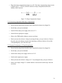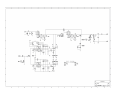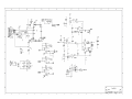
1
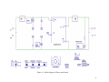
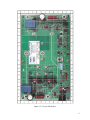
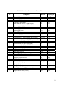
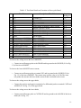
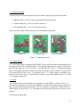
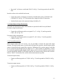
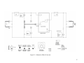
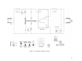
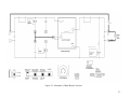
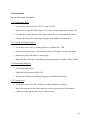
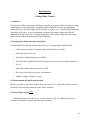
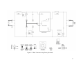
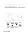
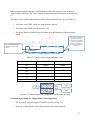
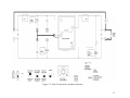
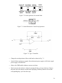
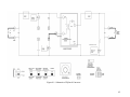
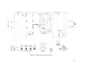
Power Electronics Laboratory User Manual Department of Electrical and Computer Engineering University of Minnesota Revised: September 8, 2011 Rev E SAFETY WARNING Before using this laboratory, read, understand and follow the Safety Precautions mentioned inside this manual. This is an educational laboratory where high-voltage terminals and large current-carrying components and circuits are exposed for ease of measurements. Therefore, regardless of the voltage and current levels, these should be treated as high voltages and high currents, and the safety precautions mentioned in the manual must be followed. Contents Exp. # Title Page Safety Precautions 3 1. Laboratory and Power-pole Board Familiarization 6 2. Buck Converter 16 3. Switching Characteristic of MOSFET and Diode 20 4. Boost Converter 23 5. Buck-Boost Converter 26 6. Voltage-Mode Control 30 7. Peak Current Mode Control 36 8. Flyback Converter 41 9. Forward Converter 45 Appendix 49 2 SAFETY PRECAUTIONS 1. Why is safety important? Attention and adherence to safety considerations is even more important in a power electronics laboratory than is required in any other undergraduate electrical engineering laboratories. Power electronic circuits can involve voltages of several hundred volts and currents of several tens of amperes. By comparison the voltages in many teaching laboratories rarely exceed 20V and the currents hardly ever exceed a few hundred milliamps. In order to minimize the potential hazards, we will use dc power supplies that never exceed voltages above 40-50V and will have maximum current ratings of 5A or less. However in spite of this precaution, power electronics circuits on which the student will work may involve substantially larger voltages (up to hundreds of volts) due to the presence of large inductances in the circuits and the rapid switching on and off of amperes of current in the inductances. For example a boost converter can have an output voltage that can theoretically go to infinite values if it is operating without load. Moreover the currents in portions of some converter circuits may be many times larger than the currents supplied by the dc supplies powering the converter circuits. A simple buck converter is an example of a power electronics circuit in which the output current may be much larger than the input dc supply current 2. Potential problems presented by Power Electronic circuits • Electrical shock may take a life. • Exploding components (especially electrolytic capacitors) and arcing circuits can cause blindness and severe burns. • Burning components and arcing can lead to fire. 3. Safety precautions to minimize these hazards 3.1 General Precautions • Be calm and relaxed, while working in Lab. • When working with voltages over 40V or with currents over 10A, there must be at least two people in the lab at all times. • Keep the work area neat and clean. • No paper lying on table or nearby circuits. • Always wear safety glasses when working with other than signal-level power. 3 • Use rubber door mats to insulate yourself from ground, when working in the Lab. • Be sure about the locations of fire extinguishers and first aid kits in lab. • A switch should be included in each supply circuit so that when opened, these switches will de-energize the entire setup. Place these switches so that you can reach them quickly in case of emergency, and without reaching across hot or high voltage components. 3.2 Precautions to be taken when preparing a circuit • Use only isolated power sources (either isolated power supplies or AC power through isolation power transformers). This helps in using a grounded oscilloscope. This reduces the possibility of risk of completing a circuit through your body. This also reduces the possibility of destroying the test equipment. 3.3 Precautions to be taken before powering the circuit • Check for all the connections of the circuit and scope connections before powering the circuit, to avoid shorting or any ground looping, that may lead to electrical shocks or damage of equipment. • Check any connections for shorting two different voltage levels. • Check if you have connected load at the output. This is very important in Boost and Buck-Boost Converters and converters based on them. • Double check your wiring and circuit connections. It is a good idea to use a pointto-point wiring diagram to review when making these checks. 3.4 Precautions while switching ON the circuit • Apply low voltages or low power to check proper functionality of circuits. • Once functionality is proven, increase voltages or power, stopping at frequent levels to check for proper functioning of circuit or for any components is hot or for any electrical noise that can affect the circuit’s operation. 3.5 Precautions while switching on or shutting down the circuit • Reduce the voltage or power slowly till it comes to zero. • Switch of all the power supplies and remove the power supply connections. 4 • Let the load be connected at the output for some time, so that it helps to discharge capacitor or inductor if any, completely. 3.6 Precautions while modifying the circuit • Switch on the circuit as per the steps in section 3.5. • Modify the connections as per your requirement. • Again check the circuit as per steps in section 3.3, and switch ON as per steps in section 3.4. 3.7 Other Precautions • No loose wires or metal pieces should be lying on table or near the circuit, to cause shorts and sparking. • Avoid using long wires, that may get in your way while making adjustments or changing leads. • Keep high voltage parts and connections out of the way from accidental touching and from any contacts to test equipment or any parts, connected to other voltage levels. • When working with inductive circuits, reduce voltages or currents to near zero before switching open the circuits. • BE AWARE of bracelets, rings, metal watch bands, and loose necklace (if you are wearing any of them), they conduct electricity and can cause burns. Do not wear them near an energized circuit. • Learn CPR and keep up to date. You can save a life. • When working with energized circuits (while operating switches, adjusting controls, adjusting test equipment), use only one hand while keeping the rest of your body away from conducting surfaces. 5 Experiment 1 Laboratory and Power-pole Board Familiarization 1.1 Introduction The power electronics laboratory is built around a reconfigurable circuit board, termed the Power-pole board, along with accessory daughterboards. The details of the Power-pole board are discussed in later sections of this experiment. This first experiment will familiarize you with the laboratory equipment and Power-pole circuit board. 1.2 Laboratory Equipment Each experiment station has the following equipment. Digital Oscilloscope with RS232 interface Function generator DC power supply 0-60 V - 2 A max ±12 V Signal Power Supply (with DIN connector output) Differential voltage probe Power Pole circuit board and associated plug-in boards with magnetic components and daughterboards with onboard components for implementing closed loop control. Digital Multimeter Desktop computer with software for capturing oscilloscope data via RS232 port. Note: The lab instructor will demonstrate how to use the software to capture oscilloscope waveforms. Students should bring floppy disks or flash drives to download the captured waveforms or data for use in their lab reports. This equipment will be used to set up the circuits and to perform most measurements. The laboratory will also have several miscellaneous components including power resistors, magnetics boards, hookup wire, etc. as needed for specific experiments. 1.3 Power-pole Board Familiarization The main feature of the Power-pole Board is the reconfigurable power-pole consisting of two MOSFETs and two diodes. The drive circuits for the MOSFETs are incorporated on the board, and so are the various protection circuits for over current and over voltage. PWM signals to control the MOSFETs can be generated onboard or supplied from an external source. The powerpole can be configured to work in various topologies using three magnetics boards (BB board for 6 buck, boost and buck-boost converters, Flyback board for flyback converter, and Forward board for forward converter) which plug into the Power-pole Board. In addition, there is an option of doing frequency analysis of each topology by injecting a small-signal sinusoidal control voltage. The board can also be operated in voltage/current feedback mode using an external control circuit mounted on a daughter board which plugs into the Power-pole Board. The basic block diagram of the Power-pole Board is shown in Fig. 1.1 and the actual board is shown in Fig. 1.2. Please note that the locations of the various components on the board are indicated in Table 1.1. 1.3.1 Power-pole The power-pole consists of MOSFETs Q10 and Q15 and diodes D10 and D15. The source of the upper MOSFET and the drain of the lower MOSFET are connected to screw terminals for external connection, and so are the anode of upper diode and the cathode of the lower diode. The voltage and current waveforms at the terminals of the MOSFETs and diodes can be observed. Table 1.2 shows the locations of test points on the power pole board. Note: Take care whenever you are using oscilloscope probes to measure voltage. If the measurement reference potential is different to the oscilloscope reference potential, you must use differential probe. To observe the voltage across the upper MOSFET, • Connect the positive and negative terminals of a differential probe to the DRAIN and SOURCE of upper MOSFET. To observe the upper MOSFET source current, • Connect the positive and negative terminals of a differential probe to terminals CS2 and SOURCE (D-2 in Fig. 1.2) of upper MOSFET. The current sense resistor value is 0.05 Ω. 7 Figure 1.1: Block diagram of Power-pole Board. 8 Figure 1.2: Power-Pole board. 9 Table 1.1: Location of components on Power-Pole board No. 1 2 3 4 5 6 7 8 9 10 11 12 13 14 15 16 17 18 19 20 21 22 23 24 25 26 27 28 29 30 31 32 33 34 Component Terminal V1+ Terminal V2+ Terminal COM (input) Terminal COM (output) DIN connector for ±12 V signal supply Signal supply switch Signal supply +12 V fuse Signal supply −12 V fuse Signal supply LED Fault LED Over voltage LED Over current LED Upper MOSFET , diode and heat sink assembly Lower MOSFET , diode and heat sink assembly Screw terminal for upper MOSFET source Screw terminal for lower diode cathode Screw terminal for upper diode anode Screw terminal for lower MOSFET drain Screw terminal for Mid-point Magnetics Board plug-in space PWM Controller UC3824 Duty ratio pot RV64 Switching frequency adjustment pot RV60 External PWM signal input terminal Selector Switch Bank Daughter board connector Switched load Resettable Fuse Control selection jumpers Ramp select jumper Current limit jumper Small-signal ac analysis selection jumper Input current sensor (LEM) Output current sensor (LEM) Ref. Des. J1 J21 J2 J22 J90 S90 F90 F95 D99 D32 D33 D34 Q15, D15 Q10, D10 J13 J11 J12 J10 J18 J20 U60 RV64 RV60 J68 S30 J60 R22 F21 J62, J63 J61 J65 J64 CS1 CS5 Location in Fig. 1.2 A-1 L-1 A-4 L-6 A-5 B-6 B-5 B-6 B-5 D-6 D-6 D-6 C-2 C-4 D-3 D-4 E-3 E-4 F-3 H-3 I-5 F-5 I-5 G-6 E-5 H-6 K-5 L-2 J-5 H-5 H-6 G-5 B-1 K-2 10 Table 1.2: Test Point Details and Location on Power-pole Board No. Test Point 1 2 3 4 5 6 7 8 9 10 11 11 12 12 13 13 14 14 15 16 V1+ V2+ CS1 CS2 CS3 CS4 CS5 CS LOAD 1 CS LOAD 2 PWM DRAIN (upper MOSFET ) SOURCE (upper MOSFET ) DRAIN (lower MOSFET ) SOURCE (lower MOSFET ) ANODE (upper diode) CATHODE (upper diode) ANODE (lower diode) CATHODE (lower diode) GATE (upper MOSFET ) GATE (lower MOSFET ) Description of Test Point Terminal V1+ Terminal V2+ Input current Upper MOSFET source current Lower diode or MOSFET source current Output Capacitor Current Output current Switched Load Voltage +ve Switched Load Voltage -ve PWM Signal Upper MOSFET drain Upper MOSFET source Lower MOSFET drain Lower MOSFET source Upper diode anode Upper diode cathode Lower diode anode Lower diode cathode Gate of upper MOSFET Gate of lower MOSFET Location in Fig. 1.2 C-1 K-1 B-4 D-2 D-4 K-3 K-4 L-5 L-5 E-6 D-2 D-2 E-4 E-4 E-2 E-2 D-4 D-4 C-2 C-4 To observe the voltage across the lower MOSFET , • Connect an oscilloscope probe to the DRAIN and its ground to the SOURCE (E-4 in Fig. 1.2) of the lower MOSFET. To observe the lower MOSFET source current, • Connect an oscilloscope probe to terminal CS3 and its ground to the SOURCE (E-4 in Fig. 1.2) of the lower MOSFET. The current sense resistor value is 0.05 Ω. The same test points also measure the lower diode current if that is included in the circuit. To observe the voltage across the upper diode, • Connect the positive and negative terminals of a differential probe to terminal CATH and ANODE (E-2 in Fig. 1.2) of the upper diode. To observe the voltage across the lower diode, • Connect an oscilloscope probe to CATHLOW and its ground to the ANODE of the lower diode (D-4 in Fig. 1.2). 11 1.3.2 Magnetics Boards To build various converters using the Power-pole Board , three plug in boards are provided: 1. BB Board (Fig. 1.3(a)): For buck, boost and buck-boost converters 2. Flyback Board (Fig. 1.3(b)): For flyback converter 3. Forward Board (Fig. 1.3(c)): For forward converter How to use these boards will be described in the subsequent experiments. (a) BB Board (b) Flyback Board (c) Forward Board Figure 1.3: Magnetics boards. 1.3.3 Signal Supply ±12 volts signal supply is required for the MOSFET drive circuits and also the measurement and protection circuits. This is obtained from a wall-mounted isolated power supply, which plugs into the DIN connector J90 (A-5 in Fig. 1.2). Switch S90 (B-6 in Fig. 1.2) controls the signal power to the board. Each time a fault occurs, turn off and turn on this switch to reset the board. The green LED D99 (B-5 in Fig. 1.2) indicates if the +12 V signal supply is available to the board. Fuses F90 (B-5 in Fig. 1.2) and F95 (B-6 in Fig. 1.2) provide protection for the +12 V and -12 V supplies respectively. 1.3.4 Load Any external load is to be connected across terminals V2+ and COM (L-1 and L-6 in Fig. 1.2). An onboard switched load is provided to facilitate the observation of the transient response of any converter built using the power-pole. Thus it is possible to periodically switch in and out a 20 Ω load (K-4 to K-6 in Fig. 1.2). The frequency and duty ratio of this load is fixed at 10 Hz and 10%. To select the switched load, 12 • Put switch 3 of selector switch bank S30 (E-5 in Fig. 1.2) to the top position (Load (SW) ON). In order to observe the switched load current, • Connect the positive and negative terminals of a differential probe to CSLOAD1 and CSLOAD2 (L-5 in Fig. 1.2). This measures the voltage across the 20 Ω resistor. • Switched load current is the measured voltage divided by 20. 1.3.5 Input/Output Voltage Measurement Test points for input/output voltage measurements are provided on the Power-pole Board. For input voltage measurement, • Connect the oscilloscope probe to test point V1+(C-1 in Fig. 1.2) and its ground to COM (D-1 in Fig. 1.2). For output voltage measurement, • Connect the oscilloscope probe to test point V2+ (K-1 in Fig. 1.2) and its ground to COM (L-1 in Fig. 1.2). 1.3.6 Current Measurement LEM current sensors (B-1, K-2 in Fig. 1.2) are provided to measure the input and output currents. The input current sensor is located after the input filter capacitor, and the output current sensor is located before the output filter capacitor. Calibration of the current sensors is such that for 1A current flowing through each, the output is 0.5 V. These signals are amplified by a factor of 2 and are brought out to the daughter board connector J60, for use in feedback current control. Currents through the MOSFETs and output capacitor are measured using current sense resistors. Refer to Table 1.2 for details of the various current measurement test points. To measure input current, • Connect oscilloscope probe to CS1 (B-1 in Fig. 1.2) and its ground to COM (D-1 in Fig. 1.2). To measure output current, • Connect oscilloscope probe to CS5 (K-4 in Fig. 1.2) and its ground to COM (L-1 in Fig. 1.2) . 13 To measure output capacitor ripple current, • Connect oscilloscope probe to CS4 (K-3 in Fig. 1.2) and its ground to COM. The current sense resistor value is 0.1 Ω. 1.3.7 MOSFET Drive Circuit The power-pole MOSFETs are driven by high side drivers IR2127. These drivers have in-built overcurrent protection using a current-sense resistor for each MOSFET (see locations C-3 and C5 in Fig. 1.2). The voltage across these sense resistors can be observed using test points provided on the board. To see the upper MOSFET current, • Connect the positive and negative terminals of a differential probe to CS2 and SOURCE of upper MOSFET . To see the lower MOSFET current, • Connect an oscilloscope probe to CS3 and its ground to SOURCE of lower MOSFET . Note: The lower diode current can also be observed using test point CS3. However the upper diode current cannot be observed. 1.3.8 PWM Signal Generation PWM signals required for the MOSFETs can be generated using the on-board PWM controller UC3824 (I-5 in Fig. 1.2). There is also an option to supply PWM signals from an external source. To use the onboard PWM, • Put switch 2 of the selector switch bank S30 (E-5 in Fig. 1.2) to its bottom position (PWM INT.). To use external PWM, • Put switch 2 of the selector switch bank S30 to its top position (PWM EXT.). • Connect the external PWM signal to the terminal J68 (G-6 in Fig. 1.2). While using the onboard PWM for operation of the power-pole in open-loop, the duty ratio can be controlled using pot RV64 (F-5 in Fig. 1.2). The duty ratio can be varied from 4% to 98%. The frequency of the PWM can be adjusted using the trim pot RV60 (I-5 in Fig. 1.2). There is a provision for providing an external ramp to the UC3824 IC. This is useful for peak current mode control. For this, remove jumper J61 (H-5 in Fig. 1.2) and use the RAMP pin on daughter board connector J60. 14 1.3.9 Frequency Analysis Frequency analysis of any converter built using the power-pole can be done by injecting a low voltage sinusoidal signal at jumper J64 (G-5 in Fig. 1.2). To do this, • Remove jumper J64. • Connect the small signal sinusoidal source at the jumper terminal J64. Note: J64 is to be shorted in all other modes of operation. 1.3.10 Power-pole Board in Feedback Control Mode The power-pole board can be operated in either open or closed loop and is selected by jumpers J62 and J63 (J-5 in Fig. 1.2). For open loop operation, • Keep J62 and J63 in the righthand positions. Closed loop operation will be described in the relevant experiment. 15 Experiment 2 Buck Converter 2.1 Objective The objective of this experiment is to study the characteristics of a buck converter. The circuit will be operated under continuous current mode (CCM) and open loop conditions (no feedback). Our main goal will be to compare the theoretical results with the experimental results. Simulation results can be obtained by performing Experiment No. 4 in PSpice based Power Electronics Laboratory User Manual. 2.2 Preparing the Setup Make the connections on the power-pole board as shown in Fig. 2.1 to use the upper MOSFET and the lower diode. • Use the magnetics board BB board for the buck converter circuit. The inductor is 100 µH. • Use a variable load resistor (RL) as a load. • Use onboard PWM signals. • Connect the ±12 signal supply at the DIN connector. Signal supply switch S90 should be OFF. 2.3 Checks before powering the circuit • Check the circuit connections as per the schematics. • Have your circuit checked by your Lab Instructor. 2.4 Powering the Circuit • Switch ON the signal supply. Check for green LED. • Adjust the duty ratio to 50%. • Adjust the switching frequency to 100kHz. • Apply input voltage Vd of 24 volts at terminals V1+ and COM. 16 Figure 2.1: Schematic of Buck Converter 17 2.5 Measurement and Waveforms Take the following measurements, 2.5.1 Varying Duty Ratio • Set the duty ratio at 50%, switching frequency at 100 kHz and RL= 10Ω. • Observe and make a copy of the output voltage and voltage across the diode. • Vary the duty ratio from 10 % to 90 % (in steps of 10%). • Measure the average output voltage for the corresponding duty ratio. • Calculate the theoretical average output voltage for the corresponding duty ratios. 2.5.2 Varying Switching Frequency • Set the duty ratio to 50 %. • Measure the peak-peak output ripple voltage and the peak-peak ripple in inductor current. • Repeat the above procedure for different switching frequencies (40 kHz , 60 kHz, 80 kHz). Make sure that output voltage (V2+) is maintained at 12V. • Observe and make a copy of the inductor current (CS5) and capacitor current (CS4) waveforms at 40kHz and at 100kHz 2.5.3 Varying Load • Set the switching frequency at 100kHz and duty ratio at 50%. • Set the load resistance RL=10Ω. • Increase the load resistance and observe the inductor current waveform. • Keep increasing the load resistance, until the buck converter enters discontinuous current mode operation. Note down the average inductor current value and make a copy of the inductor current waveform when the converter starts entering discontinuous current mode of operation. 18 2.5.4 Determining Efficiency Determine the efficiency of the buck converter at frequencies of 40 kHz and 100 kHz. • Set duty ratio at 50%. • Set load resistance RL=10Ω. • Measure the average output voltage V2+. • Measure the average output current Io. • Measure the average input voltage Vd. • Measure the average input current Ii. • Calculate the efficiency of the buck converter for the above two frequencies. 2.6 Lab Report The lab report should have a brief abstract detailing what has been done in the experiment. The remaining part of the report should consist of the information asked below along with any discussion you feel is necessary. 1. Attach a graph output voltage (V2+) versus duty ratio using data obtained in section 2.5.1. Also plot the theoretically calculated results on the same graph. Compare the two plots and comment about how the buck converter works as a variable dc step down transformer. Enclose output voltage & voltage across diode waveforms for duty ratio 50% 2. Attach a copy of the inductor current (CS5) and the capacitor current (CS4) waveforms obtained in section 2.5.2. Explain the relation between the two currents. Comment on the ripple in the inductor current for the two frequencies. 3. Plot the peak-peak ripple in the output voltage versus switching frequency using data obtained in section 2.5.2. Plot the theoretical results on the same graph. Compare the two plots. Comment on why you were asked to maintain the average output voltage constant. 4. Attach a copy of the inductor current waveforms obtained in section 2.5.3. Compare the theoretically calculated Rcrit with the observed value. 5. Comment on the difference in efficiency results obtained for two switching frequencies. 19 Experiment 3 Switching Characteristic of MOSFET and Diode using Power-Pole Board 3.1 Objective The objective of this experiment is to study the switching characteristics of power MOSFETs and power diodes using a buck converter. The circuit will be operated in open loop conditions (no feedback). Our main goal is to understand the switching behavior of these two power devices. 3.2 Preparing the Setup Construct the buck converter circuit as shown in Fig. 3.1 to use the upper MOSFET and lower diode. • Use the BB magnetics board. The inductor is 100 µH. • Use a variable load resistor as a load. • Connect ±12V the signal supply to the DIN connector. Signal supply switch S90 should be OFF. 3.3 Checks Before Powering The Circuit • Check the circuit connections as per the schematic. • have your circuit checked by your Lab Instructor 3.4 Powering the Circuit • Switch ON the signal supply. Check for green LED. • Adjust the duty ratio to 50%. • Set the switching frequency of 100kHz. • Set RL= 12Ω. • Apply input voltage Vd of 24 volts. 20 Figure 3.1: Schematic of Buck Converter 21 3.5 Measurement and Waveforms 1. Observe and make a copy of the Anode-Cathode diode voltage VAK using a differential probe and the diode current using CS3. Adjust the time base to show the switching details during turn-ON and turn-OFF. 2. Measure the forward voltage drop across the diode VFM. 3. Observe and make a copy of the Drain-Source Mosfet voltage VDS using a differential probe and Mosfet current CS1. Adjust the time base to show the switching details during turn-ON and turn-OFF. 4. Measure the voltage drop across the Mosfet during turn-ON period and estimate the rds(ON) of the Mosfet. (Note: the differential probe might have an offset, adjust your measurement based on this offset value.) 5. Measure the average load current Io, and the duty cycle of operation. 3.6 Exercises: 1. Attach the waveforms for turn-ON and turn-OFF of the diode showing the switching details by expanding the time base. 2. Calculate the conduction loss of the diode using eqn. 2A-1 in the book and the measurements from step 2 of section 3.5. 3. Attach the waveforms for turn-ON and turn-OFF the Mosfet showing the switching details by expanding the time base. 4. Estimate the rds(ON) of the Mosfet from step 4 of section 3.5 and compare with the datasheet of Mosfet IRF640N. 5. Calculate the conduction loss of the Mosfet using eqn. 2-3 in the book and the measurements from step 4 of section 3.5. 6. Using the values of conduction losses of the Mosfet and the Diode obtained through measurements, and switching losses of the Mosfet obtained through simulation (Refer to Experiment No. 2 in the PSpice-based Power Electronics Laboratory User Manual), estimate the efficiency of the converter. Compare the estimated efficiency with the efficiency obtained for the buck converter in the “Buck Converter Experiment”. 22 Experiment 4 Boost Converter 4.1 Objective The objective of this experiment is to study the characteristics of a boost converter. The circuit will be operated under CCM and openloop condition. Our main goal is to compare the theoretical results with the experimental results. For PSpice Simulation refer Exp. No. 5 in PSpice based power electronics lab manual. Note: It is important that care must be taken while doing the boost converter experiment that the load is always connected to the power-pole board. The input and output terminals in the case of the boost converter are interchanged as compared to that of the buck converter. V2+ & COM is the input and V1+ & COM is the output. 4.2 Preparing the Setup Make the connections of the power-pole board as shown in Fig. 4.1 to use the lower MOSFET and the upper diode. • Use the BB magnetics board for the boost circuit. The inductor is 100 µH. • Use a variable load resistor as a load. • Connect the ±12 signal supply to the DIN connector. Signal supply switch S90 should be OFF. 4.3 Checks before powering the circuit • Check the circuit connections as per the schematics. • Confirm that you have connected the input and output terminals correctly to source and load as shown in Fig. 4.1. • Have your circuit checked by your Lab Instructor. 4.4 Powering the Circuit • Switch ON the signal supply. Check for green LED. • Set the duty ratio to its minimum 10% and RL=20Ω. • Adjust the switching frequency to 100kHz. • Apply input voltage Vd of 10 volts at terminals V2+ and COM. 23 Figure 4.1: Schematic of Boost Converter 24 4.5 Measurements Take the following measurements, 4.5.1 Varying Duty Ratio • Vary the duty ratio from 10% to 60% (in steps of 10%). • Measure the average DC load voltage (V1+) for the corresponding values of duty ratio . • Calculate the theoretical average output voltage for the corresponding duty ratios. • Compare the observed average output voltage results with the calculated ones. 4.5.2 Varying Switching Frequency • Set the duty ratio to 50%, switching frequency to 100kHz, RL= 20Ω. • Observe and make a copy of the input current (CS5) ripple waveform @100kHz. • Measure the peak-peak input current ripple. • Repeat the above procedure for different switching frequencies (40 kHz, 60 kHz, 80 kHz). 4.5.3 Determining efficiency • Set the duty ratio to 50%. • Adjust the load resistance value to 20Ω. • Measure the efficiency at switching frequencies of 40kHz and 100 kHz. 4.6 Lab Report The lab report should consist of the information asked below, along with any discussion you feel is necessary. 1. Attach a graph of duty ratio versus output voltage using the data obtained in section 4.5.1. Also plot the theoretically calculated results on the same graph. Compare the two plots. 2. Attach a copy of the inductor current (CS5) waveform obtained in section 4.5.2. Plot the experimental and theoretically estimated input ripple current on the same graph. Compare the two graphs and comment. 3. Plot efficiency versus frequency using the data obtained in section 4.5.3. Comment on the results you obtain. 25 Experiment 5 Buck-Boost Converter 5.1 Objective The objective of the experiment is to study the characteristics of the buck-boost converter. The circuit will be operated under CCM and openloop conditions. Our main goal is to compare the theoretical results with the experimental results. For PSpice Simulation refer Exp. No. 6 in PSpice based power electronics lab manual Note: It is important that care must be taken while doing the buck-boost converter experiment that the load is always connected to the power-pole board. The input and output terminals in the case of the buck-boost converter are different as compared to that of the buck or boost converters. 5.2 Preparing the Setup Make the connections for the power-pole board as shown in Fig. 5.1 • Use the BB magnetics board for the buck-boost converter circuit. The inductor value is 100 µH. • Use a variable load resistor as a load. • Connect the ±12 signal supply to the DIN connector. Signal supply switch S90 should be OFF. 5.3 Checks before powering the circuit • Check the circuit connections as shown in Fig. 5.1. • Confirm that you have connected the input and output terminals correctly to source and load as shown in Fig. 5.1. • Have your circuit checked by your Lab Instructor. 5.4 Powering the Circuit • Switch ON the signal supply. Check for green LED. • Set the duty ratio to its minimum. • Set RL= 20Ω. • Adjust the switching frequency to 100 kHz. • Apply input voltage Vd of 10 volts at the terminals V1+ and V2+. 26 Figure 5.1: Schematic of Buck-Boost Converter 27 5.5 Measurements Take the following measurements, 5.5.1 Varying Duty Ratio • Vary the duty ratio from 10% to 70% (in steps of 10%). • Measure the average DC load voltage (V2+) for the corresponding values of duty ratio. • Calculate the average theoretical DC output voltage for the corresponding duty ratios. • Compare the observed average output voltage results with the calculated ones. 5.5.2 Varying Switching Frequency • Set the duty ratio to 60%, switching frequency to 100kHz, RL= 15Ω. • Observe and make the copy of the inductor current (CS5) ripple waveform @100kHz. • Measure the peak-peak inductor current ripple. • Repeat the above procedure for different switching frequencies 40 kHz, 60 kHz, 80 kHz. 5.5.3 Determining Efficiency • Set the duty ratio to 60%. • Adjust the load resistance to RL=15Ω. • Measure the efficiency at switching frequencies of 40 kHz and 100 kHz. 5.5.4 Varying Load • Set the duty ratio to 40%, RL= 20Ω and switching frequency to 40 kHz. • Keep increasing the load resistance until the converter enters into the discontinuous conduction mode and note the value of load resistance. 28 5.6 Lab Report The lab report should consist of the information asked below along with any discussion you feel is necessary. 1. Attach a graph of duty ratio versus output voltage (CS5) using the data obtained in section 5.5.1. Also plot the theoretically calculated results on the same graph. Compare the two plots. 2. Attach a copy of the inductor current (CS5) waveform obtained in section 5.5.2. Plot the experimental and theoretically estimated ripple current waveforms on the same graph. Compare the two graphs and comment. 3. Plot the efficiency versus frequency using the data obtained in section 5.5.3. Comment on the results you obtain. 4. Calculate the critical value of load resistance Rcrit,Buck-Boost at which the converter is in the border of Continuous-Discontinuous and compare with that obtained in section 5.5.4. 29 Experiment 6 Voltage-Mode Control 6.1 Objective The objective of this experiment is to design a controller to operate the buck converter in voltage control mode. For this experiment, a plug-in daughter board will be used to accomplish the control objective. The small-signal transfer function vo (s ) d (s ) ( d is a small-signal perturbation in the duty cycle and vo is the corresponding variation in the output voltage) must first be obtained for the buck converter. The plug-in daughter board is used to implement the voltagemode control feedback with the required open-loop gain. 6.2 Preparing the Setup and Open-Loop Mode Construct the buck converter circuit as shown in Fig. 6.1 using the BB magnetics board. • Connect and turn on the ±12vsignal supply and check for green LED. • Adjust the duty ratio to 50%. • Adjust the switching frequency to 100kHz. • Switch ON the switched load to active position using selector switch bank as shown in Fig. 6.2. • Adjust the variable load resistance RL to 10Ω. • Have your circuit checked by your Lab Instructor. • Apply DC supply voltage Vd to 30V. 6.3 Measurements in Open-Loop Operation Observe and make a copy of the output voltage waveform (V2+). Adjust the time base to show the details of the switching transients as the load is switched. 6.4 Using PSpice to find vo (s ) d (s ) Using the schematic file “buck_conv_avg.sch” (Refer to Exp. 10 in PSpice based power electronics lab manual), perform the following experiment. 30 Figure 6.1: Buck Converter using Power-pole board. 31 1. Obtain the Bode plots for the transfer function vo ( s) as shown in Fig. 4-10 of the d ( s ) textbook for the values given in this simulation. 2. Obtain the gain and the phase of the transfer function vo ( s) in part 1 at the frequency of d ( s ) 1 kHz, which will be chosen as the crossover of the open-loop transfer function GL ( s) . Figure 6.2: Selector switch position for switched load. 6.5 Type 3 Voltage Controller 32 Once you get the transfer function or the Bode-plot of the buck converter, you can design a Type-3 voltage controller. The Type-3 voltage control board has the schematic as shown in Fig. 6.3. The values of the resistors and capacitors of the voltage control board are given in Table. 6.1 • Reference value VREF can be set using the duty ratio pot. • Reference value VREF can’t be set below 10V. • For the pin details of terminal strip J60, please refer the schematic of the power-pole board. The op-amp in the dotted region is a part of the IC UC3824 which is designated asU60 on the power pole board. The numbers 9, 12 and 13 are pins of J60 port on the board Vref is generated through a potential divider on the board Figure 6.3: Voltage controller plug-in board. Table 6.1: Voltage control board component values Component Calculated Value Actual value used R1 100kΩ 100kΩ R2 20kΩ R3 10kΩ C1 22nF C2 C3 2.2nF 4.7nF J63 J62 Figure 6.4: Control selection for Voltage-Mode Control plug-in board 6.6 Preparing the Setup for Voltage-Mode Control Operation • Set the control selection jumpers J62 and J63 as shown in Fig. 6.4. • Insert the Voltage-Mode Control plug-in board in the terminal strip 60. 33 • Keep RL= 10Ω. • Switch ON the switched load to the active position using the selector switch bank as shown in Fig. 6.2. • Turn ON ±12Vsignal supply and check for green LED. • Have your circuit checked by your Lab Instructor. • Set Vd to 30V. • Use the duty cycle pot RV64 to set V2+ to 15V. 6.7 Measurements in Voltage-Mode Control Operation Observe and make a copy of the output voltage V 2+. 6.8 Lab Report The lab report should have a brief abstract detailing what has been done in the experiment. The remaining part of the report should consist of the information asked below along with any discussion you feel is necessary. vo (s ) d (s ) 1. Attach the Bode magnitude and phase plot of the small-signal transfer function from the results obtained in section 6.4 2. Obtain the following quantities from the Bode plot, GPS (s ) f c and GPS (s ) f for a c crossover frequency of 1kHz. 3. Calculate the needed phase boost boost using the values obtained through PSpice above with a required phase margin of 60 degrees 4. Calculate the controller gain at the crossover frequency given kFB 0.2 and GPWM (s ) f 0.556 c 5. Use the K-factor method described in chapter 4 of the book to design a type 3 voltage mode controller for the buck converter i.e, determine kc, z and p of the controller Gc(s). 6. Determine the values of the resistors and capacitors used to implement the controller in Fig. 6.3 and substitute them in Table 6.1. 34 7. The controller is implemented in hardware using the values given in Table 6.1 column #3. Compare the responses of the output voltage for a step load change with and without closed loop control. Attach the waveforms obtained in steps 6.3 and 6.7. 35 Experiment 7 Peak Current Mode Control 7.1 Objective In this experiment, we will be using a plug-in board to accomplish peak current mode control for a buck-boost converter. First the aspects of constant frequency peak current mode control will be explored. Then the plugin board will be used to achieve feedback voltage control of the converter. The goal is to understand how to design a peak current mode controller with voltage feedback. 7.2 Preparing setup for Open Loop Operation • Reconstruct the buck-boost converter used in Expt. 3 as in Fig. 7.1. • Turn on the signal power supply and set the switching frequency to 100 kHz and duty cycle such that output voltage Vo=12 V. • Change the switch positions of the switch bank as shown in Fig. 7.2. • Set Vd to 20 V and the variable power resistor to 20 Ω . 7.2.1 Measurements • Observe the output voltage V2+ and inductor current on the oscilloscope. • Store the waveform. 7.3 Preparing setup for closed loop operation and measurements 7.3.1 Closed Loop Operation Without Slope Compensation • Setup the control selection as in Fig. 7.3. • Remove shorting link from J61 and insert the Type 2 Controller plug-in board whose circuit is shown in Fig. 7.4 into the terminal strip J60 (The pin numbers shown in the figure correspond to pin numbers on the terminal strip). This board will add the voltage feedback to the control. • Set the duty cycle pot to minimum. • Switch ON the main power supply and set it to 25 V. 36 Figure 7.1: Peak Current mode controller schematic. 37 Figure 7.2: Switch positions for switched load. Figure 7.3: Switch Position for Closed Loop Operation Figure 7.4: Type 2 Controller • Change the switch positions of the switch bank as shown in Fig. 7.1. • Switch ON the signal power supply. Ensure that main power supply is ON before signal power supply is switched ON. • Observe the PWM and the inductor current waveforms. • Slowly increase the reference voltage by turning the duty cycle pot clockwise. Observe the point where the inductor current starts displaying oscillatory behavior. Record the corresponding duty cycle from the scope. 38 • Plug in the slope compensation jumper on to J61. The slope compensation jumper circuit is shown in Fig. 7.5. Observe how the inclusion of slope compensation affects the stability of the converter. Figure 7.5: Slope Compensation Jumper 7.3.2 Closed Loop Operation With Slope Compensation • Ensure that the plug-in board and the slope compensation jumper are plugged in. • Set the duty cycle pot to minimum. • Switch ON the main power supply and set it to 15 V. • Switch ON the signal power supply. • Observe the PWM and the inductor current waveforms. • Slowly increase the reference voltage by turning the duty cycle pot clockwise. Observe the point where the inductor current starts displaying oscillatory behavior. Record the corresponding duty cycle from the scope. 7.3.3 Dynamic Performance of Closed Loop System • Ensure that the plug-in board and the slope compensation jumper are plugged in. • Set the duty cycle pot to minimum. • Switch on the main power supply and set it to 20 V. • Switch on the signal power supply. • Slowly increase the reference voltage to 12 V by turning the duty cycle pot clockwise. • Observe the output voltage V2+ and the inductor current on the oscilloscope. Store the waveform. 39 7.4 Lab Report The lab report should have a brief abstract detailing what has been done in the experiment. The remaining part of the report should consist of the information asked below along with any discussion you feel is necessary. • Plot the output voltage Voand inductor current iL obtained in step 7.2. • What is the maximum duty ratio stable operation of the converter in step 7.3.1? Plot the inductor current waveform for stable and unstable operation. • What is the maximum duty ratio stable operation of the converter in step 7.3.2? Plot the inductor current waveform for stable and unstable operation. • Explain how slope compensation affects the range of duty cycle obtainable in constant frequency peak current mode control. • Explain why in step 7.3.1, it is important to switch on the signal power supply after turning on the main power supply. • Plot the output voltage Vo waveforms and inductor current in closed loop operations with output voltage feedback (step 7.3.3). • Comment on the effect of peak current controller on the operation of converter. 40 Experiment 8 Flyback Converter 8.1 Objective The objective of this experiment is to study the characteristics of the flyback converter using the power-pole board in open loop control mode. Our main goal is to compare the theoretical results with the experimental results. Note: It is important that care must be taken while doing the Flyback converter experiment that the load is always connected to the output in the power-pole board. 8.2 Preparing the Setup Make the connections on the power-pole board as shown in Fig. 8.1 to use the lower MOSFET. • Use the Flyback magnetics board. The turns ratio N1/N2=2 • Use a variable load resistor as a load. • Connect the ±12Vsignal supply to the DIN connector. Signal supply switch S90 should be OFF. 8.3 Checks before Powering the Circuit • Check the circuit connections as per the schematic. • Check that the lower MOSFET has been selected. • Have your circuit checked by your Lab Instructor 8.4 Powering the Circuit • Switch ON the signal supply. Check for green LED. • Set the switching frequency to 100kHz and the duty ratio to 50%. • Set RL= 10Ω. • Apply input voltage Vd of 15V at terminal V1+ and COM. 8.5 Measurements Take the following measurement, 8.5.1 Varying Duty Ratio • Vary the duty ratio from 0% to 50% (in steps of 10%). 41 Figure 8.1: Schematic of Flyback Converter 42 • Measure the average output voltage (V2+) for the corresponding values of duty ratios. • Calculate the theoretical average output voltage value for the corresponding duty ratios. • Compare the observed average output voltage results with the calculated ones. 8.5.2 Constant Duty Ratio with varying switching frequency and load • Set the duty ratio to 40%, switching frequency to 100 kHz and RL= 10Ω • Observe and make a copy of the voltage across the secondary side of the coupling inductor. • Observe and make a copy of the input current (CS1) and output current (CS5) in the same graph • Repeat the above step (make a copy of the current waveforms and not the voltage waveform) for RL= 7.5Ω @ Fs=100 kHz; RL= 10Ω @ Fs=40 kHz and RL= 7.5Ω @ Fs=40 kHz 8.6 Lab Report The lab report should consist of the information asked below along with any discussion you feel is necessary. 1. Attach a graph of duty ratio versus output voltage (V2+) using data obtained in section 8.5.1. Also plot the theoretically calculated results on the same graph. Compare the two plots. 2. Attach the copy of the voltage waveform obtained in section 8.5.2. Construct the voltage across the primary side of the coupled inductor. Label the waveform, both voltage and time axis appropriately. Note: Ignore the ringing in the waveform 3. Using the voltage waveform obtained in section 8.5.2, construct the voltage across the primary side switch. Label the waveform, both voltage and time axis appropriately. You can verify your calculation by observing the waveform on the board. Note: Ignore ringing and voltage when snubber circuit is on. 43 4. Attach the waveforms obtained in section 8.5.2 and estimate the following: (Need to be calculated for all the four operating conditions RL= 10Ω @ Fs=100 kHz; RL= 7.5Ω @ Fs=100 kHz; RL= 10Ω @ Fs=40 kHz and RL= 7.5Ω @ Fs=40 kHz a. Inductance as seen from the primary side Lm1 b. Peak to peak ripple in the flux p p given the number of turns in the primary is 42 c. Given the core area Ac=93.9mm2 what is the value of the peak flux density B̂ ? 44 Experiment 9 Forward Converter 9.1 Objective The objective of this experiment is to study the characteristics of the forward converter. The forward converter will be operated in open loop mode (no feedback). Our main goal is to compare the theoretical results with the experimental results. 9.2 Preparing the Setup Make the connections on the power-pole board as shown in Fig. 9.1 to use the lower MOSFET. • Use the Forward magnetics board. The turns ratio is 1:1:1. • Use a variable load resistor as a load. • Connect the ±12Vsignal supply to the DIN connector. Signal supply switch S90 should be OFF. 9.3 Checks before powering the circuit • Check the circuit connections as per Fig. 9.1 • Confirm that you have selected the lower MOSFET. • Have your circuit checked by your Lab Instructor. 9.4 Powering the Circuit • Switch ON the signal supply. Check for green LED. • Set the switching to 100 kHz. • Set the duty ratio to its minimum. • Set RL= 10Ω. • Apply input voltage Vd of 20 V at the terminals V1+ and COM. 45 Figure 9.1: Schematic of Forward Converter 46 9.5 Measurements Take following measurements, 9.5.1 Varying Duty Ratio • Vary duty ratio from minimum to 40% (in steps of 10%). • Measure the average output voltage (V2+) for the corresponding values of duty ratio. • Calculate the theoretical average output voltage for the corresponding duty ratios. • Compare the observed average output voltage results with the calculated ones. 9.5.2 Constant Duty Ratio with varying switching frequency and load • Set the duty ratio to 40%, switching frequency to 100 kHz and RL= 10Ω • Observe and make a copy of the voltage across the switch (Mosfet) • Observe and make a copy of the input current (CS1) and output current (CS5) in the same graph • Repeat the above step (make a copy of the current waveforms and not the voltage waveform) for RL= 7.5Ω @ Fs=100 kHz; RL= 10Ω @ Fs=40 kHz and RL= 7.5Ω @ Fs=40 kHz 9.6 Lab Report The lab report should consist of the information asked below along with any discussion you feel is necessary. 1. Attach a graph of duty ratio versus output voltage (V2+) using data obtained in section 9.5.1. Also plot the theoretically estimated results on the same graph. Compare the two plots. 2. Attach a copy of the voltage waveform across the switch obtained in section 9.5.2. Estimate theoretically the same waveform and compare. (Ignore the voltage ringing due to the leakage inductance of the transformer) 3. Attach the waveforms of input current and output current obtained in section 9.5.2. Also answer the following questions: 47 a. Why is the input current negative for some interval? b. What is the minimum value of this negative current for all four operating conditions? c. Theoretically should the above value change with load? Give reasons for your answer. 4. Estimate the following: (Need to be calculated for all the four operating conditions RL= 10Ω @ Fs=100 kHz; RL= 7.5Ω @ Fs=100 kHz; RL= 10Ω @ Fs=40 kHz and RL= 7.5Ω @ Fs=40 kHz. a. Output inductor value L. b. Core flux as given in Fig. 8-6 in the book. Number of turns in the primary is 16 and the magnetizing inductance Lm1 is 0.2mH. Hint: Use the minimum value of the negative current seen at the input. 48 APPENDIX The detailed circuit of the power-pole is attached. It consists of two sheets. 49 50 51