1
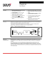
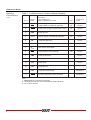
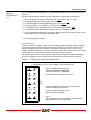
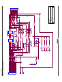
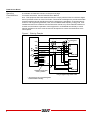
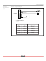
FL_101
USER MANUAL
FlashLink User Manual
CONTENTS
■
(Introduction on next page)
January 2002
1/3
FlashLink
User Manual
Features
❏
❏
❏
❏
❏
Overview
Allows PC parallel port to communicate
with PSD813F via PSDsoft
Provides interface medium for JTAG
communications
Supports basic IEEE 1149.1 JTAG
signals (TCK, TMS, TDI, TDO)
Supports additional signals to enhance
download speed (TERR, TSTAT)
Can be used for programming and/or
testing
❏
❏
❏
❏
❏
Wide power supply range of 2.7 to 5.5V
Pinout independent with target side flying
leads
Included loopback connector to validate
FlashLink and PC connection
Convenient desktop packaging allows
varying applications (desk, lab or
production)
Synchronous JTAG interface allows
speeds as fast as pc can drive
FlashLink is a hardware interface from a standard PC parallel port to one or more PSD813F
devices located within a target pc board as shown below.
This interface cable allows the PSD813F to be exercised for purposes of testing and/or
programming. PSDsoft is the software source for driving FlashLink.
Figure 1. FlashLink Adapter Application
Flying lead
cable
Mates with
PC parallel
port
12 wires Target
device
FlashLink
adapter
6 feet
6 inches
Operating
Considerations
Operating power for FlashLink is derived from the target system in the range of 2.7 to 5.5V.
Compatibility over this voltage range is ensured by the design of FlashLink. No settings are
involved.
On a cautionary note, it is recommended that the target system be powered with a well
regulated and stable source of power which is energized at the final value of VCC. It is not
recommended that the input voltage be varied using the verneer on a regulated power supply,
as this may cause the internal FlashLink IC’s (74VHC240) to misoperate toward the lower end
of the supply range.
1
FlashLink User Manual
Operating
Considerations
Table 1. Pin Descriptions for FlashLink Adapter Assembly
Signal
NSignal
ame
Name
JEN
Description
Description
JTAG = IEEE 1149.1
JTAG
=GIEEE
EJTA
= W1149.1
SI Enhanced JTAG
EJTAG = WSI Enhanced JTAG
JTAG enable on PSD813F (optional)
1
JEN
TRST
JTAG enable on PSD813F (optional)
JTAG reset on target (optional per 1149.1)
OC
OC
2
JTAG reset on target (optional per 1149.1)
Signal ground
Signal ground
Generic signal, user defined (optional)
Generic signal, user defined (optional)
JTAG test data input
JTAG test data input
OC
5
TRST
GND
GND
CNTL
CNTL
TDI
TDI
6
TSTAT
TSTAT
EJTAG programming status (optional)
EJTAG programming status (optional)
7
VCC
VCC
VDC source from target
VDC source from target
8
RST
RST
Target system reset (optional)
Target system reset (optional)
9
TMS
TMS
JTAG mode select
JTAG mode select
10 10
GGND
ND
Signaground
l ground
Signal
11 11
TC
K
TCK
JTAGclock
clock
JTAG
12 12
GGND
ND
Signaground
l ground
Signal
14 13
TD
O
TDO
JTAGserial
seriadata
l dataoutput
output
JTAG
D
estination
Destination
14 14
TERR
TE
RR
EJTAG
EJTAGprogramming
programmingerror
erro(optional)
r (optional)
Destination
D
estination
(cont.)
Pin #
Pin #
1
2
3
3
4
4
5
6
7
8
9
Notes
Notes
1.
Bold signals are required connections
1. All
Bold
signals
areare
required
connections.
2.
signal
grounds
connected
together inside FlashLink
2. OC
All signal
3.
= open grounds
collector are connected together inside FlashLink.
3. OC = open collector.
2
Type
Type
OC
OC
OC
FlashLink IS
SFlashLink
ignal: IS
Signal:
Source
Source
Source
Source
Source
Source
Source
Source
Destination
Destination
OC
OC
Source
Source
Source
Source
SoSource
urce
FlashLink User Manual
Operating
Considerations
Note: The target device must supply VCC to the FlashLink Adapter (2.7 to 5.5 VDC, 15mA max
@ 5.5V).
(cont.)
Not all 14 signals may be needed for a given application. Here’s how they break down:
❏
❏
❏
❏
❏
❏
❏
(6) Core signals that must be connected: TDI, TDO, TMS, TCK, VCC, GND
(2) Optional signals for enhanced ISP: TSTAT, TERR
(1) Optional signal to control multiplexing of the JTAG signals: JEN
(1) Optional IEEE-1149.1 signal for JTAG chain reset: TRST
(1) Optional signal to allow FlashLink to reset target system after ISP: RST
(1)* Optional generic control signal to target system from FlashLink: CNTL
(2) Two additional ground lines to help reduce EMI if a ribbon cable is used. These ground
lines “sandwich” the TCK signal in the ribbon cable.
* = Not supported initially by PSDsoft
Target Side Pinouts
There is no indsutry “standard” JTAG connector. Each manufacturer differs. ST has a specific
connector and pinout for the FlashLink programmer adapter. The connector scheme on the
FlashLink adapter can accept a standard 14 pin ribbon connector (2 rows of 7 pins on 0.1"
centers, standard keying) or any other user specific connector that can slide onto 0.025" square
posts. The pinout for the FlashLink adapter connector is shown in Figure 2.
If a standard ribbon cable is used for quick connection of the FlashLink adapter to the target
circuit card assembly, then the target system should use the pinout as shown in Figure 2.
Figure 2. JTAG Connector Recommended Pinouts
ST ENHANCED JTAG ISP CONNECTOR DEFINITION
14
13
TERR TDO
12
GND
11
TCK
10
GND
9
8
RST
Connector reference: Molex 70247-1401
TMS
7
VCC
5
6
TSTAT TDI
3
4
CNTL GND
2
TRST
VIEW: LOOKING INTO FACE OF
SHROUDED MALE CONNECTOR.
0.025" POSTS ON 0.1" CENTERS.
1
JEN
KEY
WAY
Recommended ribbon cable for quick connection of
FlashLink adapter to end product:
Samtec: HCSD-07-D-06.00-01-S-N
Digikey: M3CCK-14065-ND
Note:
TDI is a signal source on the Flashlink and should be a
signal destination on the target board
3
1
1
PA D1
S1
PA D1
S2
PA D1 4
S HIELD
(DRAIN WIRE)
(FRAME GND)
SOLDERI NG PAD PATTERN
CBL 1
D0(TCK ) DB2
1
D1(TMS) DB3
2
D2(TDI) DB4
3
D3(J EN\) DB5
4
D4(TRS T)DB6
5
D5(RS T) DB7
6
G ND
DB1 8
7
A CK N DB1 0
8
PA P
DB1 2
9
ERRN DB1 5
10
S EL
DB1 3
11
B US Y DB1 1
12
D6
DB8
13
A UTO LINE FEEDDB1 4
14
0
R80
V CC
grey
black
orgt
brnt
white
red
org
pink
yellow
green
lt gree n
4 1 48
D3
4 1 48
D2
47
R41 4 .7 K
10K
R40
2
47
47
47
47
R10
R25
R11
R9
4 7 0K
47
R7
R5
47
47
R3
47
47
R1
47
Figure 3. FlashLink Schematic
FlashLink User Manual
3
1
V CC
Q1
2 N3 9 0 4
R8
R6
R4
R2
10K
R26
13
13
11
C53
2
C54
10
12
7 4 A C05
12
7 4 A C05
U3F
R28
4 .7 K
1 UF
C50
D1
6 .2 V
U3D
2
6
10K
10K
10K
10K
0 .0 1 UF
C51
V CC
9
3
U3C
1 0 0K
R51
R38
R37
R36
R35
U3E
V CC
7 4 A C05
10
7 4 A C05
6
9
4
5
11
Y4
Y3
Y2
Y1
8
7 4 V HC2 4 0
G
A4
A3
A2
A1
U1B
R33
R32
R31
C26
R30
R23
R22
(FOR U3)
0 .0 1 UF
1 0 0K
1 0 0K
1 0 0K
10K
10K
10K
3
5
7
9
V CC
(FOR U1)
C24
7 4 A C05
U2D
19
17
15
13
11
0 .0 1 UF
7 4 A C05
4
V CC
7 4 A C05
3
10K
R39
7 4 A C05
U2B
U2A
18
16
14
12
7 4 A C05 U3B
U2C
1
R42
4 .7 K
7 4 A C05
8
5
Y1
Y2
Y3
Y4
7 4 V HC2 4 0
G
A1
A2
A3
A4
U1A
C25
R43
4 .7 K
C55
1
2
4
6
8
(FOR U2)
0 .0 1 UF
R29
4 .7 K
C58
7 4 A C05
C57
7 4 A C05
U2F
U2E
U3A
C56
1
V CC
C52
1 0 0p f
1 0 0p f
1 0 0p f
1 0 0p f
1 0 0p f
1 0 0p f
1 0 0p f
V CC
R50
R16
47
47
47
47
47
R20
R18
47
R34
1 0 0K
R19
R17
R15
R13
D4
Th ur s d a y , A p ril 0 8, 1 9 99
Dat e :
0
1 N5 8 1 7
Doc u me n t Nu m be r
Fla s h L in k PCB
Fla s h L in k S c h em a tic
R21
S iz e
B
Title
4 7 28 0 K a to Ro a d
Fre mo n t, CA 9 45 3 8
W a fe rs c ale In te g r a tio n
10
47
R14
47
47
R12
47
R81
S he e t
1
CO NTROL
TDI
TSTA TN
V CCIN
RSTN
TMS
G ND
TCK
G ND
TDO
TERRN
/JEN
TRS TN
of
1
7 0 24 7 - 1 4 0 1
MO L EX
1
2
3
4
5
6
7
8
9
10
11
12
13
14
P1
Rev
G1
4
FlashLink User Manual
Operating
Considerations
A schematic of FlashLink is shown on the previous page.
(cont.)
Note: This equipment has been tested and found to comply with the limits for a Class A digital
device, pursuant to Part 15 of the FCC Rules. These limits are designed to provide reasonable
protection against harmful interference when the equipment is operated in a commercial environment. This equipment generates, uses, and can radiate radio frequency energy and, if not
installed and used in accordance with the instruction manual, may cause harmful interference
to radio communications. Operation of this equipment in a residential area is likely to cause
harmful interference in which case the user will be required to correct the interference at his
own expense.
For further information, see the PSDsoft Users Manual.
Figure 4. Chaining Example
FlashLink
Target System, 3V or 5V
7
7
9
TMS
11
TCK
TDI 5
9
VCC
6
TSTAT
14
TERR
13
TDO
JEN 1
TRST 2
GND* 3
CNTL 4
RST 8
GND* 10
GND* 12
11
5
optional
optional
6
14
13
VCC
10K typical
1
TMS
TCK
TDI
TDO
TSTAT
TERR
PSD813Fx
optional
optional
optional
optional
optional
2
TMS
TCK
12
straight through cable
2 row, 7 position
TDI
TDO
TSTAT
TERR
PSD813Fx
JTAG Chaining example on target system
using straight through ribbon cable
* all ground pins are connected together
inside flashlink assembly
5
FlashLink User Manual
Operating
Considerations
Figure 5. Loopback Adaptor
(cont.)
J1
To FlashLink
Assembly
1
2
3
4
5
6
7
8
9
10
11
12
13
14
J2
GND
1
TDI
TSTAT
VCC
J1
GND
CON2
1
VCC
CON1
TMS
TCK
TDO
TERR
CON14
14-pin Dual Row 0.025 square
Receptacle
Output
Signal
Signal
PC Parallel Port Connector Line
(DB25 Pin No.)
JEN
STAT
SEL (11)
TDI
TSTAT
ACKN (8)
TMS
TERR
ERRN (10)
TCK
TDO
PAP (9)
6
FL_101 - USER MANUAL
Table 1. Document Revision History
Date
30-Jan-2002
2/3
Rev.
Description of Revision
1.0
Document written in the WSI format
1.1
FL_101: FlashLink User Manual
Front page, and back two pages, in ST format, added to the PDF file
Any references to Waferscale, WSI, EasyFLASH and PSDsoft 2000
updated to ST, ST, Flash+PSD and PSDsoft Express
FL_101 - USER MANUAL
For current information on PSD products, please consult our pages on the world wide web:
www.st.com/psm
If you have any questions or suggestions concerning the matters raised in this document, please send
them to the following electronic mail addresses:
[email protected]
[email protected]
(for application support)
(for general enquiries)
Please remember to include your name, company, location, telephone number and fax number.
Information furnished is believed to be accurate and reliable. However, STMicroelectronics assumes no responsibility for the consequences
of use of such information nor for any infringement of patents or other rights of third parties which may result from its use. No license is granted
by implication or otherwise under any patent or patent rights of STMicroelectronics. Specifications mentioned in this publication are subject
to change without notice. This publication supersedes and replaces all information previously supplied. STMicroelectronics products are not
authorized for use as critical components in life support devices or systems without express written approval of STMicroelectronics.
The ST logo is registered trademark of STMicroelectronics
All other names are the property of their respective owners
© 2002 STMicroelectronics - All Rights Reserved
STMicroelectronics group of companies Australia - Brazil - Canada - China - Finland - France - Germany - Hong Kong India - Israel - Italy - Japan - Malaysia - Malta - Morocco - Singapore - Spain - Sweden - Switzerland - United Kingdom - United States.
www.st.com
3/3