1
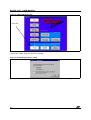
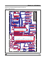
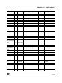
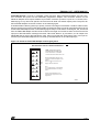
DK4000-C167 USER MANUAL Development Kit for PSD4000 and C167 CONTENTS ■ A COUPLE OF DEFINITIONS ■ HARDWARE ■ SOFTWARE ■ DETAILED DESCRIPTIONS ■ OTHER BOARD FEATURES – Step-By-Step Instructions for ISP Programming ■ USING DK4000 AS A DEVELOPMENT PLATFORM FOR C167CR USERS The DK4000 – C167 Development Board is specific to the Infineon C167CR micro-controller family. However, other proliferation boards will be available. Check the website at www.st.com/psd as to availability. – Concept A COUPLE OF DEFINITIONS – Downloading to the Development Board In-System Programming (ISP) - A JTAG interface (IEEE 1149.1 compliant) is included on the PSD enabling the entire device to be rapidly programmed while soldered to the circuit board (Main Flash memory, Secondary Boot Flash memory, the PLD and all configuration areas). This requires no MCU participation, so the PSD can be programmed or reprogrammed anytime, anywhere, even while completely blank. The MCU is completely bypassed. – JTAG - ISP ■ Congratulations on purchasing ST's DK4000 Development kit. The DK4000 (110 or 220 volt version) is a low cost kit for evaluating the PSD4000 series of Flash Programmable System Devices called PSDs. The DK4000 kit is extremely versatile, and can be used in several different modes. It can be used to demonstrate the PSD4000's capability of JTAG In-System Programmability (ISP). Once initial code is resident in the PSD, the program code can be updated while the MCU is running, called In-Application Programming (IAP). Also, Infineon C167CR family users can utilize the DK4000 as an evaluation platform for code development. 167 DESIGN OVERVIEW – Memory Swapping in the PSD – What really happens – Creating your own IAP code bundle ■ REFERENCES ■ APPENDIX In-Application Programming (IAP) – Since two independent Flash memory arrays are included in the PSD, the MCU can execute code from one memory while erasing and programming the other. Robust product firmware updates in the field are possible over any communication channel (a few examples are CAN, Ethernet, UART, J1850) using this unique architecture. For IAP, all code is updated through the MCU. HARDWARE ■ October 2001 PSD4000 Flash PSD (Programmable System Device) - see www.st.com/psd for data sheet. PSD4135G2 - 4Mbit Main Flash memory (512Kx8), 256Kbit Boot Flash memory (32Kx8), 64Kbit SRAM (8Kx8) 1/27 DK4000-C167 - USER MANUAL ■ Eval/Demo Board with C167CR or other MCU, LCD Display, JTAG and UART ports for ISP/IAP ■ FlashLINK JTAG ISP Programmer (uses PC’s parallel port) ■ Straight through serial cable (Male-Female) ■ Power Supply SOFTWARE To ensure you have the latest versions, check the website often. ■ PSDsoft Express - Point and Click Windows programming development software. This will install to it’s own directory. – MCU Selection by manufacturer and part number – Graphical definition of pin functions – Easy creation of memory map – JTAG ISP Programming. ■ Downloadable demonstration software – Visit the development tools section of ST PSM product division website at www.st.com/psd to download the file 167_disk.zip. The development boards ship with the hardware test (hwtest.obj) file already resident. A detailed description of this software bundle is included in Appendix B. The following table is a specific listing of the files contained in the 167_disk.zip file including the directory to which the file automatically extracts them. 2/27 DK4000-C167 - USER MANUAL Table 1. Listing of the files and destinations in 167_disk.zip Directory root Files Description demo10.h86 alternate firmware to load to demonstrate IAP iap.mmf memory map file for PSDload iap.obj object file to load directly into PSD iap.psd configuration file for psdload 166p_hwt_10s_.zip contains all PSDsource files 166c_hwt_10s_.zip contains all c level code files readme.txt late breaking information hwtest.obj object file to load directly into PSD u67eemop10_.zip contains all PSD source files u67democ10_.zip contains all c level code filed readme.txt late breaking information a16xbhe.obj object file to load directly into PSD 166p10iap.zip contains all PSD source files 166c10iap.zip contains all c level code files readme.txt late breaking information iap.mmf memory map file for PSDload iap.obj object file to load directly into PSD 166c10demo.zip contains all c level code files demo10.h86 alternate firmware to load to demonstrate IAP readme.txt late breaking information hwtest-167 demo-167 iap_167 demo_iap_167 Note: 1. Hex file carries the extension *.h86 from the Keil tools. 2. Infineon Dave 2.0 cd was used in these projects 3. Keil compiler version is 4.03 or later. See readme file for particulars. 3/27 DK4000-C167 - USER MANUAL DETAILED DESCRIPTIONS Figure 1. DK4000 Development Board JTAG Programming port Serial Port Provision for chaining port ST10 or Infineon C167CR PSD4135G2 SRAM provision Power switch Expansion Ports LED’s DC Power Input 2x16 character LCD display Reset Button LCD contrast adjustment 4 position DIP switch The following features are included in the development board and shown graphically in the above figure. ■ Display - A two line by 16 character LCD display is included on the Development Board. ■ Power switch ■ UART Serial Port(female) - Connected to MCU serial port; used for In-Application Programming (IAP) ■ Infineon C167CR or other MCU ■ PSD4000 software - The PSD4000 is programmed with C167CR demonstration code. User can program alternative programs via JTAG ISP. ■ JTAG programming Port - Used in conjunction with FlashLINK programmer for ISP. ■ Reset Button - For resetting the MCU and PSD ■ Pads for additional SRAM - The resident PSD4000 contains 8KB SRAM. This site is for additional SRAM. OTHER BOARD FEATURES Other features of the DK4000 board are listed below. These elements unpopulated to provide lowest cost to the user. ■ Provision for C167CR boot elements are provided with JP5, 6 and 7. ■ Provision for chaining JTAG connector is provided in P2 and JP2. ■ Provision for C167CR OWE control is provided in JP8 ■ Provision for an analog Vref input is provided in JP9 4/27 DK4000-C167 - USER MANUAL ■ Provision for off expansion is provided by board connectors suitable for 0.025 square posts ■ Provision for 9v battery input is provided near power connector (solder pads only). Step-By-Step Instructions for ISP Programming a) Install PSDsoft Express on your PC running Windows 95/98/NT/2000. Check web for latest version. b) Plug the FlashLINK Programmer into your PC’s parallel port and plug in the ribbon cable to the JTAG port on the eval board (for help, see the Appendix C, FlashLINK manual). c) Plug in power supply and turn on power. An LCD contrast control is provided as R11. The typical setting is near the counterclockwise stop. d) Run PSDsoft Express. Here is the initial screen if no project was open. Figure 2. Opening screen upon PSDsoft Express invocation Use cancel at this point since all we need to do is program the PSD with an existing demonstration file (*.obj) and there is no need to create a new project. Later, in the “Using the DK4000 as a development platform”, a further tutorial is given on using PSDsoft Express with the Eval Board for development. Figure 3. Invocation reminder screen e) In the Design Flow (shown below), click on the ST JTAG/ISP button. Bottom row of boxes left side. 5/27 DK4000-C167 - USER MANUAL Figure 4. PSDsoft Express flow Click here The following screen appears inquiring if it’s desired to program a single device or multiple devices in the JTAG chain. Select “Only one” and then click OK. Figure 5. JTAG-ISP Operations dialog Clicking OK brings up the JTAG Operations - Single device dialog shown in the following figure. 6/27 DK4000-C167 - USER MANUAL Figure 6. PSDsoft Express, JTAG Operations dialog AI05709 f) In Step 1, browse to find the *.obj file shown in the above figure g) In “select device” box, choose the PSD4000 device you have installed on the board h) In step 3, select the operation of “Program”. Click execute. i) Observe in the lower pane the JTAG activities that occur while programming your device. j) Watch the display. When the download is completed as indicated in the log window, push the reset button on the Development Board. The displays below will sequence one time and then operation will stop. Figure 7. Eval Board Displays for IAP.obj N o t n e e d o E a s y i * * * s f e a r F L A S H h e r e ! C O M P L E T E ! ! ! * * * 7/27 DK4000-C167 - USER MANUAL If you cycle power to the board, you will see that the display will resequence, confirming that the program and all configuration information are stored in the PSD’s non-volatile Flash memory. k) For better understanding of the program you may want to examine the following references: 1. System memory map in the “167 Design Overview” section of this document. 2. PSDsoft Express project (a16xbhe.ini) 3. The file source code (included) to see how the executing code was configured Notice: An additional code bundle will be posted on the web in the future to cover the IAP functionality. Please go to www.st.com/psd, and select “Development Tools” and scroll down to DK4000. Latest software and manual can then be downloaded. USING DK4000 AS A DEVELOPMENT PLATFORM FOR C167CR USERS Concept ■ The ST DK4000 Development Board provides the following capabilities ■ Demonstrate design concepts early, optimizing “time to market” ■ Jump start user application with proven framework (hardware and software) ■ Substitute for user target system until target prototypes are available ■ Gives instant platform for testing ISP and IAP demonstration. ■ Allows programming the PSD using included Flashlink cable Downloading to the Development Board Executable code can be downloaded to the Development Board two different ways; via the JTAG (ISP) or via the UART (IAP). This manual only describes the ISP capabilities at this time. The IAP capabilities will be supported in the future using PSDload available on the website at www.st.com/psd. JTAG - ISP The PSD4000 series JTAG interface provides the capability of programming all memory areas within the PSD (PLD, configuration, MAIN and secondary Flash memories). This interface can also be used to program a completely blank component as JTAG is enabled as the default PSD state. See Application Note 54 (AN054) for further description of the JTAG interface on our CD or our website at www.st.com/psd . The LCD will be non operational during JTAG - ISP, since the MCU is not operating. During this interval, the PSD is not connected to the MCU bus. To restrain the MCU during this interval, the JTAG interface contains a signal,!RST, that is connected to the MCU reset pin. ST provides a FlashLINK programmer to facilitate the JTAG programming operation. The FlashLINK programmer connects the PC parallel port to the Eval Board JTAG header and is driven by PSDsoft Express, the PSD development tool. 167 DESIGN OVERVIEW The following figure depicts how the memory is allocated in this project for the hwtest.obj. Hwtest.obj uses the segmented mode of the C167CR. The demo1 project uses the non-segmented mode of the C167CR. The C167CR contains a large addressable memory area that is partitioned into segments of 64k bytes each. Even though many memory segments exist in the C167CR, only segments 0 and 1 are used in this 8/27 DK4000-C167 - USER MANUAL project. The configuration of the C167CR is controlled by two registers that are written at system startup (syscon and buscon0). These registers handle the mechanism for different bus width peripherals in the C167CR as well as many other items. See the C167CR user manual for details. Additional areas can be controlled by the definition of pairs of buscon and addr registers for each discrete area. The project definitions of these registers are denoted in the memory map figure below. The default configuration (syscon and buscon0) is 16 bit multiplexed for the following system resources; ■ C167 resources ■ PSD code memory (main and secondary Flash memory and boot areas) ■ PSD SRAM Two additional areas are defined as 8 bit multiplexed as shown below for the following system resources. ■ LCD ■ CSIOP space (PSD registers). The C167CR XRAM and CAN areas are not used. Figure 8. Memory map of DK4000/167 Board 0x0FFFF 0x1FFFF 167 System Area 0x0C000 CSIOP(PSD),buscon1 LCD, buscon1 0x0BF00 0x0BE00 0x0A000 PSD RAM 4Kx16 0x08000 Flash PSD, FS0 32Kx16 0x04000 Code PSD Boot area (csboot0,1) x16 0x10000 0x0 Segment 0 Segment 1 Boot Configuration AI05706 Note: Default x16 multiplex bus used (syscon and buscon0) unless otherwise noted Memory Swapping in the PSD For this test (hwtest.obj), the dip switch should be in the following position . As a component of this test, a copy of the executing code that resides in csboot0/1 is made. The destination of this copy is 9/27 DK4000-C167 - USER MANUAL the main Flash memory area FS0, as shown in the figure below. After the copy operation, the following map applies. Figure 9. Memory map after running of hwtest.obj 0x0FFFF 0x1FFFF 167 System Area 0x0C000 CSIOP(PSD),buscon1 LCD, buscon1 0x0BF00 0x0BE00 0x0A000 0x08000 PSD RAM 4Kx16 Flash PSD, FS0 32Kx16 0x04000 Copy of code from csboot0,1 PSD Boot area (csboot0,1) message (boot area) 0x0 Segment 0 0x10000 message (main flash) Segment 1 AI05707 Notice in the above figure the element denoted as message in each of the code areas. This element is displayed as the second LCD screen to show the source of execution. For normal boot, the second LCD screen shows “executing from, BOOT area”. The message exists in a fixed location in the code and is read from this location and copied to the LCD at boot up. When the code copy is performed, a different message is inserted into the same fixed location based on the destination of the copy (as shown in FS0). When this version of the code is executed, the message is displayed “executing from MAIN FLASH”. This method yields a single unambiguous confirmation of the execution source, which is very convenient for demonstrating memory swapping operations. 10/27 DK4000-C167 - USER MANUAL Now let’s boot from the other memory to demonstrate the swapping capability of the PSD. Place the dip switch in the following position and press the reset button. You should see the execution source annunciated to the display “booting from MAIN FLASH”. The following memory map applies. Figure 10. Memory map for alternate memory boot 0x0FFFF 0x1FFFF 167 System Area 0x0C000 CSIOP(PSD),buscon1 LCD, buscon1 0x0BF00 0x0BE00 0x0A000 PSD RAM 4Kx16 0x08000 0x04000 Main Flash code copy from csboot0,1 message (main flash) 0x0 Segment 0 0x10000 Segment 1 AI05708 The memory movement within the MCU memory map is accomplished via the logic contained in the PLD equations in the PSD. Each segment that moves must have dual ranged defined in these equations. The selection is made based on a single logic bit (exe_src_a) that resides in the PSD PAGE register. Following are the equations for the system. These can bee seen in the PSDsoft Express project included with the kit. Note that “#” indicates a logical OR and “&” indicates a logical AND Csboot0 = (0x0 – 0x01FFF) & !exe_src_a Csboot1 = (0x02000 – 0x03FFF) & !exe_src_a Fs0 = ( (0x10000 – 0x1FFFF) & !exe_src_a ) # ( ( 0x0 – 0x03FFF) & exe_src ) Note that the logic variable (bit) controlling the actual location of the memory is “exe_src_a”. When this bit is zero (0), the memory segments are as shown in figure 9. When exe_src_a is one (1), FS0 appears in the execution location and the csboot areas are not in the map at all. The physical location of this logic bit, exe_src_a, is in the bit6 position of the PAGE register. Actually this bit can be anywhere, the only important element is that it is contained in the PLD equations as shown above and accessible by the MCU. Control of this bit is via a board mounted dip switch. The power up sequence is as follows: 1. Execute start167.a66 2. Read the dip switch 11/27 DK4000-C167 - USER MANUAL 3. Write the dip switch setting into the PSD PAGE register (some positioning is done prior to the write). Once the PAGE register write operation has completed, the next instruction is fetched from the new memory location (FS0). This same sequence of events occurs every time power is applied to the board. Since the PAGE register is always 00h at power up, the software always executes steps a) and b) from the boot area. Then, based on the dip switch selection, the code will either stay in the boot area or jump to the main Flash memory area. What really happens There is a subtlety involved in the transfer of execution described above. This subtlety is because the MCU really doesn’t know the source of the instruction bytes; boot area or main Flash memory. All the MCU knows is that valid instructions on valid address boundaries are presented on the bus when the MCU needs them. Then the MCU executes the instruction and generates the next address. The key element involved is the generation of the address by the MCU. To understand this critical transfer of control, let’s examine the instruction by instruction transition from one memory to the other. After the reset signal is deasserted, the MCU is executing from the csboot area normally. This continues until the exe_src_a bit is written, moving FS0 into the execution location (0x00x3FFF). At this same time, csboot area is, for all practical purposes, gone from the system memory map. At this point, the MCU is generating the next address from the instruction received from the csboot area. However, the next instruction will come from the FS0 area. This next instruction fetch must be appropriate to maintain the program flow. That is, the next instruction must be received by the MCU on an instruction boundary and be appropriate for the program flow. In addition, any issues with the stack and stack pointer must be resolved so program flow can continue (subroutine return addresses, temporary variables, etc.). Pipelining operations can result in execution from the pipeline instead of the new memory, but the pipeline will continue to be filled from the new memory. The method we’ve used to ensure correct operation is to place identical code at identical locations in both applications through the point of the swap. After the point of the swap, the code bundles can diverge without problems. While this result is inherently ensured in a code copy scenario like hwtest.obj, it’s not so automatic when the applications are different such as exists in a true IAP scenario. Creating your own IAP code bundle A few easy steps can ensure that program flow for this critical area is guaranteed to occur properly. These steps involve the absolute location of certain modules within the base application and the new IAP application. Locating these modules is accomplished using linker controls. With this framework, booting from one application to another is EASY. REFERENCES IEEE Std 1149.1-1990 IEEE Test Access Port and Boundary Scan Architecture Flashlink User Manual (included in the Appendix of this document) AN1153 Application note: JTAG Information AN1426 Application note: Design Guide, PSDsoft Express and PSD4135G2 12/27 DK4000-C167 - USER MANUAL APPENDIX Appendix A - Jumper configuration on DK4000. Jumper Default position (shown by dotted line) Description JP1 Measure PSD current JP2 JTAG chaining JP3 Internal / external power supply JP4 9v battery connector Board position No measure Upper center No chain Upper right Internal power supply Lower right None (no jumper) Lower right Figure 11. Assembly Drawing with default jumper positions JTAG, P1 JP1 PSD I Meas serial port NO CHAIN JP2 PSD MCU area Power Supply Int Ext LCD Contrast LCD Display on off JP3 battery connection d7-14 Power on indicator AI05339 Appendix B Software functional description. Hwtest. This code exercises all components of the development board; the display, PSD memory and chip selects, and the UART channel (single character only on receive and transmit). This confirms functionality and is used as a production test. The following list is a detailed description of the viewable LCD screens. ■ Invocation banner, software version ■ Display execution source. (boot area or main Flash memory) ■ Motherboard LED test ■ PSD RAM test 13/27 DK4000-C167 - USER MANUAL ■ Code Copy. Executing boot code is copied to main Flash memory block FS0 (BOOT-> FLASH) ■ Displays Flash memory ID and does erase of FS0 prior to the copy operation. ■ UART test (waiting for host to send “0”, development board reply is a “1”, baud rate is19200 with 8 data bits, no parity and one stop bit) This software also includes provision for external SRAM test in evaltest.c but this code is not utilized at this time since the site is unpopulated. If this code is used, be aware that the appropriate buscon must be set for 8 bit demuxed bus. After this code has run one time, a copy of the executing code exists in the Flash memory area (FSx). The system can run from this code copy by placing the dip switch in the appropriate configuration as described in the “Memory Swapping in the PSD” section of this document. Demo1. This is a simple program that displays the following text on the LCD display. No Need to fear, EASYflash is here!!!!. The intent is to show a minimal level of functionality. No UART support is provided. 14/27 1 2 3 4 MR 1 2 3 4 5 6 7 8 9 10 11 12 13 14 15 16 17 18 19 20 P3 MAX6315 2 3 GND VCC P3.15 P3.0 P3.1 P3.2 P3.3 P3.4 P3.5 P3.6 P3.7 P3.8 P3.9 P3.10 P3.11 P3.12 P3.13 RESET DB9F U4 R2 100 0.1 0.1 C5 C6 0805 1 2 3 4 5 6 7 8 9 10 11 12 13 14 15 16 17 18 19 20 A GND VCC P5.0 P5.1 P5.2 P5.3 P5.4 P5.5 P5.6 P5.7 P5.8 P5.9 P5.10 P5.11 P5.12 P5.13 P5.14 P5.15 RESET S1 !RESET !MR !MR VCC 100 R6 T1out T2out R1in R2in V- V+ VCC U3 R4 14 7 13 8 6 2 16 R57 100 P4 0.1 1 6 RS-232 2 7 3 R3 100 8 4 9 5 J4 VCC C7 22pf C2 10k R5 P8.[7..0] 1 2 3 4 5 6 7 8 9 10 11 12 13 14 15 16 17 18 19 20 JP9 P8.0 P8.1 P8.2 P8.3 P8.4 P8.5 P8.6 P8.7 P7.0 P7.1 P7.2 P7.3 P7.4 P7.5 P7.6 P7.7 Vref Agnd GND VCC VCC P7.[7..0] 137 138 2 JP8 37 84 9 10 11 12 13 14 15 16 emulator 2 P8.0 P8.1 P8.2 P8.3 P8.4 P8.5 P8.6 P8.7 19 20 21 22 23 24 25 26 1 2 3 4 5 6 7 8 P6.0 P6.1 P6.2 P6.3 P6.4 P6.5 P6.6 P6.7 P7.0 P7.1 P7.2 P7.3 P7.4 P7.5 P7.6 P7.7 27 28 29 30 31 32 33 34 35 36 39 40 41 42 43 44 P5.0 P5.1 P5.2 P5.3 P5.4 P5.5 P5.6 P5.7 P5.8 P5.9 P5.10 P5.11 P5.12 P5.13 P5.14 P5.15 P3.0 65 P3.1 66 P3.2 67 P3.3 68 P3.4 69 P3.5 70 P3.6 73 P3.7 74 P3.8 75 P3.9 76 TXD0 P3.10 77 RXD0 P3.1178 79 P3.12 80 P3.13 81 P3.15 RXD0 TXD0 P6.[7..0] P8.[7..0] P6.[7..0] 3 xx_MHz RXD0 TXD0 P5.[15..0] 11 10 12 9 P5.[15..0] P5 C4 C3 0.1 5 0.1 4 3 1 P3.[13..0] T1in T2in R1out R2out C2- C2+ C1- C1+ 2 1 2 1 xx_MHz Y2 1 2 3 3 1 2 3 Y1 4 10M R1 3 1 VCC VCC Vref OW E P8.0/CC16IO P8.1/CC17IO P8.2/CC18IO P8.3/CC19IO P8.4/CC20IO P8.5/CC21IO P8.6/CC22IO P8.7/CC23IO P7.0/POUT0 P7.1/POUT1 P7.2/POUT2 P7.3/POUT3 P7.4/CC28IO P7.5/CC29IO P7.6/CC30IO P7.7/CC31IO P6.0/!CS0 P6.1/!CS1 P6.2/!CS2 P6.3/!CS3 P6.4/!CS4 P6.5/!HOLD P6.6/!HLDA P6.7/!BREQ B Agnd !RSTIN !RSTOUT !NMI P2.0/CC0IO P2.1/CC1IO P2.2/CC2IO P2.3/CC3IO P2.4/CC4IO P2.5/CC5IO P2.6/CC6IO P2.7/CC7IO P2.8/CC8IO/EX0IN P2.9/CC9IO/EX1IN P2.10/CC10IO/EX2IN P2.11/CC11IO/EX3IN P2.12/CC12IO/EX4IN P2.13/CC13IO/EX5IN P2.14/CC14IO/EX6IN P2.15/CC15IO/EX7IN P1H7 P1H6 P1H5 P1H4 P1H3 P1H2 P1H1 P1H0 P1L7 P1L6 P1L5 P1L4 P1L3 P1L2 P1L1 P1L0 !RD !WR/!WRL !READY ALE !EA P4.0/A16 A17 A18 A19 A20 A21 A22 P4.7/A23 AD8 AD9 AD10 AD11 AD12 AD13 AD14 AD15 AD0 AD1 AD2 AD3 AD4 AD5 AD6 AD7 A16 A17 A18 A19 A20 A21 A22 A23 !RD !WR/WRL !READY !EA P1H7 P1H6 P1H5 P1H4 P1H3 P1H2 P1H1 P1H0 P1L7 P1L6 P1L5 P1L4 P1L3 P1L2 P1L1 P1L0 P2.0 P2.1 P2.2 P2.3 P2.4 P2.5 P2.6 P2.7 P2.8 P2.9 P2.10 P2.11 P2.12 P2.13 P2.14 P2.15 85 86 87 88 89 90 91 92 95 96 97 98 99 135 134 133 132 131 130 129 128 125 124 123 122 121 120 119 118 47 48 49 50 51 52 53 54 57 58 59 60 61 62 63 64 P6.[7..0] !NMI 140 !RESET 141 142 !NMI ADIO8 ADIO9 ADIO10 ADIO11 ADIO12 ADIO13 ADIO14 ADIO15 108 111 112 113 114 115 116 117 VCC 10k R55 VCC 10k R54 ADIO0 ADIO1 ADIO2 ADIO3 ADIO4 ADIO5 ADIO6 ADIO7 100 101 102 103 104 105 106 107 CNTL1(_RD) CNTL0(_WR) CNTL2(_BHE) C167CR P5.0/AN0 P5.1/AN1 P5.2/AN2 P5.3/AN3 P5.4/AN4 P5.5/AN5 P5.6/AN6 P5.7/AN7 P5.8/AN8 P5.9/AN9 P5.10/AN10/T6UED P5.11/AN11/T5UED P5.12/AN12/T6IN P5.13/AN13/T5IN P5.14/AN14/T4UED P5.15/AN15/T2UED P3.0/T0IN P3.1/T6OUT P3.2/CAPIN P3.3/T3OUT P3.4/T3EUD P3.5/T4IN P3.6/T3IN P3.7/T2IN P3.8/MRST P3.9/MTSR P3.10/TXD0 P3.11/RXD0 P3.12/!BHE/!WRH P3.13/SCLK P3.15/CLKOUT XTAL2 XTAL1 U1 0.01 C38 B Vss Vss Vss Vss Vss 143 139 127 110 94 Vss Vss Vss Vss Vss 83 71 55 45 18 22pf C1 3 1 144 136 126 109 93 Vcc Vcc Vcc Vcc Vcc 82 72 56 46 17 Vcc Vcc Vcc Vcc Vcc Agnd 38 1 ADIO8 ADIO9 ADIO10 ADIO11 ADIO12 ADIO13 ADIO14 ADIO15 ADIO0 ADIO1 ADIO2 ADIO3 ADIO4 ADIO5 ADIO6 ADIO7 U2 1 2 3 JP1 71 72 73 74 75 76 77 78 79 80 1 2 GND VCC P6.0 P6.1 P6.2 P6.3 P6.4 P6.5 P6.6 P6.7 P1L[7..0] C 1 2 3 4 5 6 7 8 9 10 11 12 13 14 15 16 17 18 19 20 P6 PE[7..0] !RESET39 PE0 PE1 PE2 PE3 PE4 PE5 PE6 PE7 PD0 PD1 PD2 PD3 C18 0.1 P2.[15..0] PE[7..0] PA0 PA1 PA2 PA3 PA4 PA5 PA6 PA7 PB0 PB1 PB2 PB3 PB4 PB5 PB6 PB7 51 52 53 54 55 56 57 58 61 62 63 64 65 66 67 68 GND VCC 1 2 3 4 5 6 7 8 9 10 11 12 13 14 15 16 17 18 19 20 P7 A8 A9 A10 A11 A12 A13 A14 A15 21 22 23 24 25 26 27 28 41 42 43 44 45 46 47 48 A0 A1 A2 A3 A4 A5 A6 A7 C19 1 31 32 33 34 35 36 37 38 P2.0 P2.1 P2.2 P2.3 P2.4 P2.5 P2.6 P2.7 P2.8 P2.9 P2.10 P2.11 P2.12 P2.13 P2.14 P2.15 PSD42xxG GND PC0 PC1 PC2 PC3 PC4 PC5 PC6 PC7 !RESET PB0 PB1 PB2 PB3 PB4 PB5 PB6 PB7 PA0 PA1 PA2 PA3 PA4 PA5 PA6 PA7 PG0 PG1 PG2 PG3 PG4 PG5 PG6 PG7 PF0 PF1 PF2 PF3 PF4 PF5 PF6 PF7 3 PE0(TMS) PE1(TCK/ST) PE2(TDI) PE3(TDO) PE4(TSTAT/RDY) PE5(TERR) PE6(VSTBY) PE7(VBATON) PD0(ALE) PD1(CLKIN) PD2(!CSI) PD3(!WRH) CNTL0(_WR) 59 CNTL1(_RD) 60 CNTL0(!WR) CNTL1(!RD) CNTL2(_BHE) 40 CNTL2(!BHE) ADIO8 13 ADIO9 14 ADIO10 15 ADIO11 16 ADIO12 17 ADIO13 18 ADIO14 19 ADIO15 20 ADIO0 3 ADIO1 4 ADIO2 5 ADIO3 6 ADIO4 7 ADIO5 10 ADIO6 11 ADIO7 12 Icc mea s VCC C 2 9 29 69 Vcc_1 Vcc_1 Vcc_1 GND GND GND GND GND 8 30 49 50 70 GND VCC P1H7 P1H6 P1H5 P1H4 P1H3 P1H2 P1H1 P1H0 P1L7 P1L6 P1L5 P1L4 P1L3 P1L2 P1L1 P1L0 left side A16 A17 A18 A19 A20 A21 A22 A23 PB[7..0] PA[7..0] A[15..8] 4 6 5 DS1 RS E R/W 1 2 3 4 5 6 7 8 9 10 11 12 13 14 15 16 17 18 19 20 P8 S2 PB7 PB6 PB5 PB4 PD[3..0] D A0 PB2 1 2 3 4 5 6 7 8 9 10 11 12 13 14 15 16 17 18 19 20 P9 10K typ VCC R10 R9 R8 R7 A[7..0] 100pf C40 PB0 PB1 1 D 1 2 3 JP10 3 2 1 2 3 4 8 7 6 5 Date: Size B Title A23 A22 A21 A20 A19 A18 A17 A16 PD0 PD1 PD2 PD3 CNTL0(_WR) CNTL1(_RD) CNTL2(_BHE) !RESET PE6 PE7 GND VCC D7 D6 D5 D4 D3 D2 D1 D0 GND V0 Vcc HC16201-A (NORM) (XA) R11 10K 2 PB0 GND VCC PB7 PB6 PB5 PB4 PB3 PB2 PB1 PB0 PA7 PA6 PA5 PA4 PA3 PA2 PA1 PA0 PB0 12 11 10 9 8 7 6 5 27 26 23 25 4 28 3 31 2 1 2 3 4 5 6 7 8 9 10 11 12 13 14 15 16 17 18 19 20 P11 Monday, July 17, 2000 Document Number DK4000 CS1 A0 A1 A2 A3 A4 A5 A6 A7 A8 A9 A10 A11 A12 A13 A14 A15 A16 U5 ADIO15 ADIO14 ADIO13 ADIO12 ADIO11 ADIO10 ADIO9 ADIO8 ADIO7 ADIO6 ADIO5 ADIO4 ADIO3 ADIO2 ADIO1 ADIO0 E Sheet 0.1 C8 GND VCC PA[7..0] E ADIO[15..0] PB4 22 A0 A1 A2 A3 A4 A5 A6 A7 A8 A9 A10 A11 A12 A13 A14 PB2 PB3 DK4000 Development Board, 167CR PD[3..0] 1 2 3 4 5 6 7 8 9 10 11 12 13 14 15 16 17 18 19 20 P10 14 13 12 11 10 9 8 7 1 3 2 VCC A[23..16] ADIO[15..0] 3 1 A 1 29 24 30 13 14 15 17 18 19 20 21 of 1 2 3 4 5 6 7 8 9 10 11 12 13 14 15 16 17 18 19 20 P12 MS628128 WE OE CS2 D0 D1 D2 D3 D4 D5 D6 D7 A[15..8] A[7..0] 4 2 Rev C 0.1 C9 GND VCC A14 A15 A12 A13 A10 A11 A8 A9 A7 A6 A5 A4 A3 A2 A1 A0 1 2 3 CNTL0(_WR) CNTL1(_RD) VCC ADIO0 ADIO1 ADIO2 ADIO3 ADIO4 ADIO5 ADIO6 ADIO7 A[23..16] DK4000-C167 - USER MANUAL Appendix C Development Board Schematic and parts list Figure 12. Main Schematic 15/27 DK4000-C167 - USER MANUAL Figure 13. Power Supply Schematic 16/27 DK4000-C167 - USER MANUAL Table 2. DK4000 Parts List Ref Des Qua Generic Part ntity Number Description Vendor Part Number 1 pcbevm0002 asian 21insq, us 25 in sq@ ds1 1 dis101-0001 display y1 1 y101-0002 crystal, 16MHZ u1 1 umcu0002 microcontroller infineon C161V u2 1 PSD42xxG ST PSD42xxG psd socket Yamiachi IC149-080-030-S5 hantronix hdm16216h-b vfsmc-316pf11.0592 u3 1 u232-0001 232 driver analog devices adm202jrn u4 1 usup0002 max 6315 maxim, 5v max6315leuk u6 1 ureg-0001 regulator micrel mic5237-5.0bt d1-4 4 cr101-0001 diode d5 1 vr101-0001 zener diode, 15v motorola mmsz5254bt1 d6 1 cr101-0002 signal diode national fdLL4148 d7-15 9 led101-0002 led, t5(t1.75) lumex SLX-LX5093ID c1-2 2 cap0805-2209 22 pf caps, cer murata grm40c0g22050ad c10,c21,c23,c25 4 cap1206-1004 cap, 1uf tant murata grm42-6y5v105z016ad c12,c19 2 cap1206-1004 cap, 1uf cer, 1206 AVX 1206zc105mat2a 18 cap0805-1003 0.1 cap, smt, cer murata grm40z5u104z016ad c3-9,c11, c1318,c20,c22, c24 s1ab C40 1 cap0805-1009 r1 1 res0805-1005 resistor, smt, 10M, 1/8 watt, 0805 samsung rm10j106ct r2-4, R57 3 res0805-1000 resistor, smt, 100, 1/8 watt samsung rm12j101ct res0805-1002 resistor, smt, 10k, 1/8 watt, 0805 samsung rm10f1002ct digikey 3309P-103-ND r5-10, r12-r23, r32-47, R54, R55 35 r11 1 variable resistor, 10k R24-31, R53 9 res0805-8200 resistor, smt. 820, 1/8 watt jp1, jp3 2 con225-1003 3 position header samtec tsw-103-23-L-s-LL j1,j3 2 rec225-1002 shunt (use with jpx above) samtec snt-100-bk-g jp2 1 con225-3003 post 3x3 samtec tsw-103-23-L-T-LL j2 1 rec225-3002 triple shunt (use with jp3) samtec mnt-103-bk-g j4 1 con232-0001 rt angle rs232 connector(female, 9 pin) amp 745988-4 s1 1 sw102-0001 reset switch, momentary bourns 7914g s2 1 swdip0004 4 position dip switch,side actuated cts 195-4mst s3 0 sw101-0002 on-off switch digikey EG1906-ND t1 1 tr101-0001 class 2 transformer, 500ma,female digikey dpd090050-p-5 j7 1 con103-0001 connector for ps, male digikey pj-202a rm10f820ct 17/27 DK4000-C167 - USER MANUAL Ref Des Qua Generic Part ntity Number 1 Part Number samtec con104-2007 jtag connectors samtec tst-107-01-L-D-LL 1 con225-1014 14 pin single in line connector/ spacer (display) samtec dw-14-17-T-S-250-LL 4 std102-0250 standoffs for board richco SRS4-5-01 2 std101-0250 standoffs for display, 0.250 richco dlcbsat-4-01 2 tp101-0001 test points koa rcw 2 riv101-0281 rivet rivet king c-1 (std tubular rivet) 1 P13-P16 4 18/27 Vendor 7x2 ribbon connector p1 tp_ps,tp_gnd Description DK4000-C167 - USER MANUAL Appendix D: FlashLINK Users Manual Features. ■ Allows PC parallel port to communicate with PSD4000 via PSDsoft Express ■ Provides interface medium for JTAG communications ■ Supports basic IEEE 1149.1 JTAG signals (TCK, TMS, TDI, TDO) ■ Supports additional signals to enhance download speed (!TERR, TSTAT) ■ Can be used for programming and/or testing ■ Wide power supply range of 2.7 to 5.5V ■ Pinout independent with target side flying leads ■ Convenient desktop packaging allows varying applications (desk, lab or production) ■ Synchronous JTAG interface allows speeds as fast as pc can drive. Overview. FlashLINK is a hardware interface from a standard PC parallel port to one or more PSD4000 devices located within a target PC board as shown below. This interface cable allows the PSD to be exercised for purposes of programming and/or testing. PSDsoft Express is the source for driving FlashLINK. Figure 14. Typical FLASHlink application Flying lead cable Mates with PC parallel port 12 WIRES FlashLink adapter Target device 6 feet 6 inches AI05342 Operating considerations. Operating power for FlashLINK is derived from the target system in the range of 2.7 to 5.5 V. Compatibility over this voltage range is ensured by the design of FlashLINK. No settings are involved. On a cautionary note, it is recommended that the target system be powered with a well regulated and stable source of power which is energized at the final value of V CC. It is not recommended that the input voltage be varied using the verneer on a regulated power supply, as this may cause the internal FlashLINK ICs (74VHC240) to misoperate toward the lower end of the supply range. Each FlashLINK is packaged with a six-inch “flying lead” cable for maximum adaptability (a ribbon cable requires the use a certain connector on the target assembly). This flying lead cable mates to the FlashLink adapter on one end and has loose sockets on the other end to slide onto 0.025 square posts on the target assembly. 19/27 DK4000-C167 - USER MANUAL Table 3. Pin descriptions for FlashLINK adapter assembly DESCRIPTION JTAG = IEEE 1149.1 EJTAG = ST EHANCED JTAG PIN # SIGNAL NAME 1 JEN\ 2 TRST\ * 3 GND 4 CNTL * 5 TDI 6 TSTAT 7 Vcc 8 RST\ Target system reset (recommended) 9 TMS JTAG mode select 10 GND Signal ground 11 TCK JTAG clock 12 GND Signal ground 13 TDO JTAG serial data output Destination 14 TERR\ EJTAG programming error (optional) Destination Note: 1. 2. 3. 4. 5. Type Flashlink is Signal Enables JTAG pins on PSD8XXF (optional) OC,100K Source JTAG reset on target (optional per 1149.1) OC,10K Source OC,100K Source Signal ground Generic control signal, (optional) JTAG serial data input Source EJTAG programming status (optional) Destination VDC Source from target (2.7 - 5.5 VDC) Bold signals are required connections all signal grounds are connected inside FlashLink adapter OC = open collector, pulled-up to Vcc inside FlashLink adapter * = Not supported initially by PSDsoft. The target device must supply Vcc to the FlashLink Adapter (2.7 to 5.5 VDC, 15mA OC,10K Source Source max @ 5.5V). All 14 signals may not be needed for a given application. Here’s how they break down: (6) Core signals that must be connected: TDI, TDO, TMS, TCK, Vcc and GND (2) Optional signals for enhanced ISP: TSTAT, TERR\ (1) Optional signal to control multiplexing of the JTAG signals: JEN\ (1) Recommended signal to allow FlashLINK to reset target system during and after ISP: RST\ (1) Optional IEEE-1149.1 signal for JTAG chain reset: TRST\ (1) Optional generic control signal from FlashLink to target system: CNTL (2) Two additional ground lines to help reduce EMI if a ribbon cable is used. These ground lines “sandwich” the TCK signal in the ribbon cable. These lines are not needed for use with the flying lead cable. That is why the flying lead cable has only 12 of 14 wires populated. 20/27 Source DK4000-C167 - USER MANUAL FlashLINK pinouts. There is no “standard” JTAG connector. Each manufacturer differs. ST has a specific connector and pinout for the FlashLINK programmer adapter. The connector scheme on the FlashLink adapter can accept a standard 14 pin ribbon connector (2 rows of 7 pins on 0.1" centers, standard keying) or any other user specific connector that can slide onto 0.025" square posts. The pinout for the FlashLINK adapter connector is shown in the following figure. A standard ribbon cable is good way to quickly connect to the target circuit board. If a ribbon cable is used, then the receiving connector on the target system should be the same connector type with the same pinout as the FlashLINK adapter shown in the following figure Keep in mind that the JTAG signal, TDI, is sourced from the FlashLINK adapter and should be routed on the target circuit card so that it connects to the TDI input pin of the PSD device. Although the name “TDI” infers “Data In” by convention, it is an output from FlashLINK and an input to the PSD device. Also, keep in mind that the JTAG signal, TDO, is an input received by the FlashLINK adapter and is sourced by the PSD device on the TDO output pin. Figure 15. Pinout for FlashLINK Adapter and Target System WSi ENHANCED JTAG ISP CONNECTOR DEFINITION 14 VIEW: LOOKING INTO FACE OF SHROUDED MALE CONNECTOR. 0.025" POSTS ON 0.1" CENTERS. 13 TERR TDO 12 Connector reference: Molex 70247-1401 11 GND TCK 9 10 GND TMS 8 7 RST VCC 6 5 TSTAT TDI 4 3 CNTL GND 2 1 TRST JEN KEY WAY Recommended ribbon cable for quick connection of FlashLink adapter to end product: Samtec: HCSD-07-D-06.00-01-S-N or Digikey: M3CCK-14065-ND Note: TDI is a signal source on the Flashlink and a signal destination on the target board. TDO is a signal destination on the FlashLink and a signal source on the target board. AI05343 21/27 DK4000-C167 - USER MANUAL Figure 16. JTAG Chaining Example Target System, 3v or 5v FlashLink Vcc 7 Adapter Conncetor Vcc 7 9 TMS TCK 11 9 TDI 5 5 TSTAT 6 !TERR 14 1 TMS 11 optional optional TDO 13 !JEN 1 optional 2 optional !TRST 3 GND* 4 optional CNTL 8 recommended !RST GND* 10 GND* 12 TCK TDI TDO 6 14 TSTAT TERR\ PSD4000 13 1 2 3 4 8 10 12 TMS TCK TDI TDO Any JTAG Device in ByPass Mode * all ground pins are connected together inside FlashLINK assembly TMS TCK straight through ribbon cable 2 row, 7 position JTAG Chaining Example, PSD4000 and other JTAG compatible devices. 2 n TDI TDO System Reset Circuitry TSTAT TERR\ PSD4000 AI05344 22/27 1 2 3 4 PAD1 1 S1 PAD1 1 S2 PAD14 A SHIELD (DRAIN WIRE) (FRAME GND) 0 grey black orgt brnt white R80 red org pink yellow green lt green 4148 D3 4148 D2 R41 4.7K 470K 47 47 47 47 47 10K R40 2 R10 R25 R11 R9 47 R7 R5 47 47 R3 47 47 R1 47 VCC Q1 2N3904 R8 R6 R4 R2 B 10K R26 B 13 13 11 1 VCC 2 10 74AC05 12 74AC05 U3F 12 74AC05 U2F 1UF C50 1 2 4 6 8 5 C25 D1 6.2V (FOR U2) Y1 Y2 Y3 Y4 C U3D 2 6 10K 10K 10K 10K C 0.01UF C51 VCC 9 3 U3C R38 R37 R36 R35 100K R51 VCC 74AC05 10 U3E 74AC05 6 9 4 5 11 Y4 Y3 Y2 Y1 8 74VHC240 G A4 A3 A2 A1 R33 R32 R31 C26 R30 R23 R22 (FOR U3) 0.01UF 100K 100K 100K 10K 10K 10K 3 5 7 9 VCC (FOR U1) C24 U1B 74AC05 U2D 19 17 15 13 11 0.01UF 74AC05 4 VCC 74AC05 3 10K R39 74AC05 U2B U2A 18 16 14 12 74AC05 U3B U2C 1 R42 4.7K 74VHC240 G A1 A2 A3 A4 U1A 74AC05 8 R43 4.7K 100pf C55 R28 4.7K 0.01UF R29 4.7K U2E 74AC05 U3A C57 C56 C58 C54 C53 C52 100pf 100pf 100pf 100pf 100pf 100pf A 3 1 1UF C61 VCC 4 47 47 47 U4 D R16 R14 R12 47 47 47 47 4.7K 2 3 R20 R18 R34 100K R52 47 R19 R17 R15 R13 D4 Document Number FlashLink PCB Thursday, May 18, 2000 0 1UF C60 R53 1N5817 Date: FlashLink Schematic R21 Size B Title 47280 Kato Road Fremont, CA 94538 Waferscale Integration EN IN 10 47 47 R50 OUT D GND 1 SOLDERING PAD PATTERN CBL1 D0(TCK)DB2 1 D1(TMS) DB3 2 D2(TDI) DB4 3 D3(JEN\)DB5 4 D4(TRST) DB6 5 D5(RST) DB7 6 GND DB18 7 ACKN DB10 8 PAP DB12 9 ERRN DB15 10 SEL DB13 11 BUSY DB11 12 D6 DB8 13 AUTO LINE FEED DB14 14 R81 10 Sheet 1 E CONTROL TDI TSTATN VCCIN RSTN TMS GND TCK GND TDO TERRN /JEN TRSTN E of 1 Rev G PHONEJACK J1 70247-1401 MOLEX 1 2 3 4 5 6 7 8 9 10 11 12 13 14 P1 1 2 3 4 DK4000-C167 - USER MANUAL Figure 17. Loop back connector schematic 23/27 DK4000-C167 - USER MANUAL Figure 18. Loop Back Tester, Passive, FlashLINK J1 to FlashLINK assy 1 2 3 4 5 6 7 8 9 10 11 12 13 14 J2 GND 1 GND CON2 TDI !TSTAT VCC J1 1 VCC CON1 TMS TCK TDO !TERR CON14 14 pin dual row 0.025 sq receptacle(polarized) PC signal output PC signal input PC line connector TDI !TSTAT ACKN (8) TMS !TERR ERRN (10) TCK !TDO PAP (9) AI05346 Appendix E Results codes and debug tree for 8031_f1.obj Results codes. Table 4. Hexadecimal to Binary Conversion binary Results = abcd 0 0000 1 0001 2 0010 3 0011 4 0100 5 0101 6 0110 7 0111 8 1000 9 1001 A 1010 B 1011 C 1100 D 1101 E 1110 F 1111 24/27 Success Code DK4000-C167 - USER MANUAL Table 5. Debug Tree a b c d action x x x 1 Page register test Replace PSD ( u1 on EVD) and retest x x 1 x PSD ram error Replace PSD ( u1 on EVD) and retest x 1 x x External Ram error Replace sram (u3 EVM) and retest 1 x x x Uart error Repair u4 or surrounding circuitry, EVM (this is under the EVD board) Note: X = don’t care Appendix F: Board errata Following is a brief list of issues with correlated on a revision level basis Rev B. Center row of connections for U5 contain solder mask. This row is intended for a socket to accommodate 0.3" wide SRAM. Also pin 16 is left out. These will be corrected at next board rev. 25/27 DK4000-C167 - USER MANUAL Table 6. Document Revision History Date 19-Oct-2001 26/27 Rev. Description of Revision 1.0 Document written in the WSI format 2.0 Document converted to the ST format DK4000-C167 - USER MANUAL For current information on PSD products, please consult our pages on the world wide web: www.st.com/psd If you have any questions or suggestions concerning the matters raised in this document, please send them to the following electronic mail addresses: [email protected] [email protected] (for application support) (for general enquiries) Please remember to include your name, company, location, telephone number and fax number. Information furnished is believed to be accurate and reliable. However, STMicroelectronics assumes no responsibility for the consequences of use of such information nor for any infringement of patents or other rights of third parties which may result from its use. No license is granted by implication or otherwise under any patent or patent rights of STMicroelectronics. Specifications mentioned in this publication are subject to change without notice. This publication supersedes and replaces all information previously supplied. STMicroelectronics products are not authorized for use as critical components in life support devices or systems without express written approval of STMicroelectronics. The ST logo is registered trademark of STMicroelectronics All other names are the property of their respective owners. 2001 STMicroelectronics - All Rights Reserved STMicroelectronics GROUP OF COMPANIES Australia - Brazil - China - Finland - France - Germany - Hong Kong - India - Italy - Japan - Malaysia - Malta - Morocco Singapore - Spain - Sweden - Switzerland - United Kingdom - U.S.A. www.st.com 27/27