1
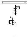
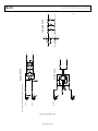
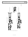
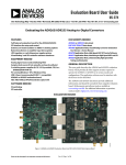
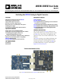
AD9286-500EBZ User Guide
UG-191
One Technology Way • P.O. Box 9106 • Norwood, MA 02062-9106, U.S.A. • Tel: 781.329.4700 • Fax: 781.461.3113 • www.analog.com
Evaluating the AD9286 Analog-to-Digital Converter
FEATURES
DOCUMENTS NEEDED
Full featured evaluation board for the AD9286
SPI interface for setup and control
Support LVDS output mode option
External or on-board oscillator options
Balun/transformer or amplifier input drive options
Switching power supply
VisualAnalog™ and SPIController software interfaces
AD9286 data sheet
HSC-ADC-EVALCZ data sheet
AN-905 Application Note, VisualAnalog Converter Evaluation
Tool Version 1.0 User Manual
AN-878 Application Note, High Speed ADC SPI Control Software
AN-877 Application Note, Interfacing to High Speed ADCs via SPI
AN-835 Application Note, Understanding High Speed ADC
Testing and Evaluation
EQUIPMENT NEEDED
Analog signal source and antialiasing filter
Sample clock source (if not using the on-board oscillator)
Two switching power supplies (6.0 V, 2.5 A),
CUI EPS060250UH-PHP-SZ, provided
PC running 32-bit Windows® XP, Window Vista, or Windows 7
USB 2.0 port, recommended (USB 1.1-compatible)
AD9286 evaluation board
HSC-ADC-EVALCZ FPGA-based data capture kit
SOFTWARE NEEDED
VisualAnalog
SPIController
GENERAL DESCRIPTION
This user guide describes the AD9286 evaluation board,
which provides all of the support circuitry required to operate
the AD9286 in its various modes and configurations. The
application software used to interface with the device is also
described.
The AD9286 data sheet provides additional information and
should be consulted when using the evaluation board. All
documents and software tools are available at the FIFO page.
For additional information or questions, send an email to
[email protected].
TYPICAL MEASUREMENT SETUP
9286CE01
REV A
AD9286
9286CE01A
09346-001
HSC-ADC-EVALCZ
Figure 1. AD9286 Evaluation Board and HSC-ADC-EVALCZ Data Capture Board
PLEASE SEE THE LAST PAGE FOR AN IMPORTANT
WARNING AND LEGAL TERMS AND CONDITIONS.
Rev. A | Page 1 of 24
UG-191
AD9286-500EBZ User Guide
TABLE OF CONTENTS
Features .............................................................................................. 1
Input Signals...................................................................................3
Equipment Needed ........................................................................... 1
Output Signals ...............................................................................3
Software Needed ............................................................................... 1
Default Operation and Jumper Selection Settings ....................4
Documents Needed .......................................................................... 1
Evaluation Board Software Quick Start Procedures .....................5
General Description ......................................................................... 1
Configuring the Board .................................................................5
Typical Measurement Setup ............................................................ 1
Using the Software for Testing.....................................................5
Revision History ............................................................................... 2
Evaluation Board Schematics and Artwork ...................................9
Evaluation Board Hardware ............................................................ 3
Ordering Information .................................................................... 22
Power Supplies .............................................................................. 3
Bill of Materials ........................................................................... 22
REVISION HISTORY
6/14—Rev. 0 to Rev. A
Changes to Figure 13 ........................................................................ 9
Changes to Figure 14 ...................................................................... 10
Changes to Figure 15 ...................................................................... 11
Changes to Figure 16 ...................................................................... 12
Changes to Figure 17 ...................................................................... 13
Changes to Figure 18 ...................................................................... 14
Changes to Figure 19 ...................................................................... 15
REVISION HISTORY
5/11—Revision 0: Initial Version
Rev. A | Page 2 of 24
AD9286-500EBZ User Guide
UG-191
EVALUATION BOARD HARDWARE
on the PCB before connecting to the low dropout linear regulators
(default configuration) that supply the proper bias to each of the
various sections on the board.
The AD9286 evaluation board provides all of the support
circuitry required to operate the AD9286 in its various modes
and configurations. Figure 2 shows the typical bench characterization setup used to evaluate the ac performance of the
AD9286 . It is critical that the signal source used for the analog
input and clock have very low phase noise (<1 ps rms jitter) to
realize the optimum performance of the signal chain. Proper
filtering of the analog input signal to remove harmonics and
lower the integrated or broadband noise at the input is necessary
to achieve the specified noise performance.
INPUT SIGNALS
When connecting the clock and analog source, use clean signal
generators with low phase noise, such as the Rohde & Schwarz SMA,
or HP8644B signal generators or an equivalent. Use a 1 m shielded,
RG-58, 50 Ω coaxial cable for connecting to the evaluation
board. Enter the desired frequency and amplitude (see the
specifications in the AD9286 data sheet). When connecting the
analog input source, a multipole, narrow-band, band-pass filter
with 50 Ω terminations is recommended. Analog Devices, Inc.,
uses TTE and K&L Microwave, Inc., band-pass filters. The
filters should be connected directly to the evaluation board.
See the Evaluation Board Software Quick Start Procedures
section to get started, and see Figure 13 to Figure 25 for the
complete schematics and layout diagrams. These diagrams
demonstrate the routing and grounding techniques that
should be applied at the system level when designing application boards using the AD9286 .
POWER SUPPLIES
This evaluation board comes with a wall-mountable switching
power supply that provides a 6 V, 2 A maximum output. Connect
the supply to the rated 100 V ac to the 240 V ac wall outlet at
47 Hz to 63 Hz. The output from the supply is provided through
a 2.1 mm inner diameter jack that connects to the printed circuit
board (PCB) at J101. The 6 V supply is fused and conditioned
If an external clock source is used, it should also be supplied
with a clean signal generator as previously specified. Typically,
most Analog Devices evaluation boards can accept ~2.8 V p-p or
13 dBm sine wave input for the clock.
OUTPUT SIGNALS
The default setup uses the Analog Devices high speed converter
evaluation platform (HSC-ADC-EVALCZ) for data capture.
WALL OUTLET
100V TO 240V AC
47Hz TO 63Hz
SWITCHING
POWER
SUPPLY
SWITCHING
POWER
SUPPLY
SIGNAL GENERATOR
6V DC
2A MAX
6V DC
2A MAX
CLOCK SOURCE
SIGNAL GENERATOR
ANALOG FILTER
9286CE01
REV A
AD9286
9286CE01A
09346 -002
HSC-ADC-E VALCZ
PC RUNNING
VisualAnalog
AND SPIController
USER SOFTWARE
Figure 2. Evaluation Board Connection
Rev. A | Page 3 of 24
UG-191
AD9286-500EBZ User Guide
Clock Circuitry
DEFAULT OPERATION AND JUMPER SELECTION
SETTINGS
This section explains the default and optional settings or modes
allowed on the AD9286 evaluation board.
Power Circuitry
Connect the switching power supply that is supplied in the
evaluation kit between a rated 100 V ac to 240 V ac wall outlet
at 47 Hz to 63 Hz and J101.
Analog Input
The default clock input circuit on the AD9286 evaluation
board uses a simple transformer-coupled circuit using a high
bandwidth 1:1 impedance ratio transformer (T501) that adds a
very low amount of jitter to the clock path. The clock input is
50 Ω terminated and ac-coupled to handle single-ended sine wave
types of inputs. The transformer converts the single-ended input to
a differential signal that is clipped by CR501 before entering the
ADC clock inputs. The AD9286 board has on-chip circuitry to
distribute a single clock to each interleaved ADC channel.
Alternatively, the AD9286 evaluation board supports driving
each internal ADC core with its own separate half speed clock.
This is useful in applications where the user wants to externally
control the clock timing per channel. To enable separate
clocking, write a value 0 to SPI Address 0x09 and place a
jumper across J204 to tie AUXCLKEN to DRVDD.
The analog input on the evaluation board default configuration
uses a single transformer input with a 50 Ω impedance. The
default analog input configuration supports analog input frequencies of up to ~200 MHz. This input network is optimized
to support a wide frequency band.
An alternate analog input configuration uses a single
ADA4937-1 ultralow distortion amplifier, which drives both
VIN1 and VIN2. Special attention has been paid to provide a
symmetrical layout between the two differential inputs to
realize best performance. To configure the analog input
circuitry, see Table 1.
Non-SPI Mode
The nominal input drive level is 10.5 dBm to achieve 1.2 V p-p full
scale into 50 Ω. At higher input frequencies, slightly higher input
drive levels are required due to losses in the front-end network.
VREF
The AD9286 operates with a fixed 1.0 V reference. This sets the
analog input span to 1.2 V p-p.
For users who want to operate the DUT without using SPI,
remove the shorting jumpers on J302. This disconnects the
CSB, SCLK, and SDIO/PWDN pins from the SPI control bus,
allowing the DUT to operate in non-SPI mode. In this mode,
the SDIO/PWDN pin takes on an alternate function to enable
power-down functionality.
To enable the power-down feature, add a shorting jumper across
J202 at Pin 2 and Pin 3 to connect the SDIO/PDWN pin to
DRVDD.
RBIAS
RBIAS has a default setting of 10 kΩ (R206) to ground and is
used to set the ADC core bias current. Note that using a resistor
value other than a 10 kΩ, 1% resistor for RBIAS may degrade
the performance of the device.
Table 1. Analog Input Mode Configurations 1
Analog Input Mode
Passive Path
Active Path
1
R406
DNI
0Ω
R407
0Ω
DNI
R408
0Ω
DNI
R409
DNI
0Ω
DNI = do not install.
Rev. A | Page 4 of 24
R410
33 Ω
DNI
R411
33 Ω
DNI
R412
33 Ω
0Ω
R413
33 Ω
0Ω
AD9286-500EBZ User Guide
UG-191
EVALUATION BOARD SOFTWARE QUICK START PROCEDURES
This section provides quick start procedures for using the AD9286
evaluation board. Both the default and optional settings are
described.
CONFIGURING THE BOARD
3.
4.
5.
6.
Figure 3. VisualAnalog, New Canvas Window
2.
Figure 4. VisualAnalog Default Configuration Message
3.
USING THE SOFTWARE FOR TESTING
Setting Up the ADC Data Capture
After configuring the board, set up the ADC data capture using
the following steps:
1.
After the template is selected, a message appears asking if
the default configuration can be used to program the FPGA
(see Figure 4). Click Yes to close the window.
09346-004
2.
Connect the evaluation board to the data capture board, as
shown in Figure 1 and Figure 2.
Connect one 6 V, 2.5 A switching power supply (such as
the CUI, Inc., EPS060250UH-PHP-SZ) to the AD9286
board.
Connect one 6 V, 2.5 A switching power supply (such
as the supplied CUI EPS060250UH-PHP-SZ) to the
HSC-ADC-EVALCZ board.
Connect the HSC-ADC-EVALCZ board to the PC with a
USB cable.
On the ADC evaluation board, confirm that six jumpers
are installed as described as follows:
• J103, Pin 2 and Pin 3 (clock with regulator)
• J104, Pin 2 and Pin 3 (amp with regulator)
• J105, Pin 2 and Pin 3 (DRVDD with regulator)
• J106, Pin 2 and Pin 3 (AVDD with regulator)
• J201, Pin 1 and Pin 2 (SCLK SPI)
• J202, Pin 1 and Pin 2 (SDIO SPI)
On the ADC evaluation board, use a clean signal generator
with low phase noise to provide an input signal to the desired
A and/or B channel(s). Use a 1 m, shielded, RG-58, 50 Ω
coaxial cable to connect the signal generator. For best results,
use a narrow-band band-pass filter with 50 Ω terminations
and an appropriate center frequency. (Analog Devices uses
TTE, Allen Avionics, and K&L band-pass filters.)
Open VisualAnalog on the connected PC. The appropriate part type should be listed in the status bar of the
VisualAnalog – New Canvas window. Select the template
that corresponds to the type of testing to be performed (see
Figure 3).
Note that once power is applied to the AD9286 evaluation
board, the device is powered down. To wake up the device,
the SDIO/PWDN pin must be pulled low. This occurs
automatically by VisualAnalog after you complete Step 1.
Rev. A | Page 5 of 24
To change features to settings other than the default settings,
click the Expand Display button, located on the bottom
right corner of the window, to see what is shown in Figure 6.
Detailed instructions for changing the features and capture
settings can be found in the AN-905 Application Note,
VisualAnalog Converter Evaluation Tool Version 1.0 User
Manual. After the changes are made to the capture settings,
click the collapse display button (see the collapsed display
in Figure 5).
09346-005
1.
09346-003
Before using the software for testing, configure the evaluation
board using the following steps:
Figure 5. VisualAnalog Window Toolbar, Collapsed Display
AD9286-500EBZ User Guide
09346-006
UG-191
Figure 6. VisualAnalog Main Window
Rev. A | Page 6 of 24
AD9286-500EBZ User Guide
UG-191
3.
Setting Up the SPIController Software
After the ADC data capture board setup is complete, set up
the SPIController software using the following procedure:
Open the SPIController software by selecting Start >
SPIController or by double-clicking the SPIController
software desktop icon.
If prompted for a configuration file, select the appropriate
one. If not, check the title bar of the window to determine
which configuration is loaded. If necessary, choose Cfg
Open from the File menu and select the appropriate file
based on your part type. Note that the CHIP ID(1) field
should be filled to indicate whether the correct SPI
controller configuration file is loaded (see Figure 7).
09346-009
1.
In the ADCBase 0 tab of the SPIController window, you
can access all global register settings (see Figure 9). See the
AD9286 data sheet; the AN-878 Application Note, High
Speed ADC SPI Control Software; and the AN-877
Application Note, Interfacing to High Speed ADCs via SPI,
for additional information.
Figure 9. SPIController, ADC Base0
09346-007
4.
Figure 7. SPIController, CHIP ID(1) Box
Click the New DUT button in the SPIController window
(see Figure 8).
09346-008
Figure 8. SPIController, New DUT Button
09346-010
2.
Note that other settings can be changed on the ADCBase 0
page (see Figure 9) and the ADC 0 and ADC 1 pages (see
Figure 10) to set up the part in the desired mode. The
ADCBase 0 page settings affect the entire part, whereas
the settings on the ADC 0 and ADC 1 pages affect the
selected channel only. See the AD9286 data sheet; the
AN-878 Application Note, High Speed ADC SPI Control
Software; and the AN-877 Application Note, Interfacing to
High Speed ADCs via SPI, for additional information on
the available settings.
Figure 10. SPIController, ADC 0 Page
Rev. A | Page 7 of 24
UG-191
5.
AD9286-500EBZ User Guide
Troubleshooting Tips
Click the Run button in the VisualAnalog toolbar (see
Figure 11).
If the FFT plot appears abnormal, do the following:
•
09346-011
•
Figure 11. Run Button in VisualAnalog Toolbar, Collapsed Display
Adjusting the Amplitude of the Input Signal
If the FFT appears normal but the performance is poor, check
the following:
The next step is to adjust the amplitude of the input signal for
each channel as follows:
1.
If you see a normal noise floor when you disconnect the
signal generator from the analog input, be sure you are not
overdriving the ADC. Reduce the input level, if necessary.
In VisualAnalog, click the Settings button in the Input
Formatter block. Check that Number Format is set to the
correct encoding (offset binary by default). Repeat for the
other channel.
Adjust the amplitude of the input signal so that the fundamental is at the desired level (examine the Fund Power
reading in the left panel of the VisualAnalog Graph - AD9286
FFT window). See Figure 12.
•
•
•
•
Make sure an appropriate filter is used on the analog input.
Make sure the signal generators for the clock and the
analog input are clean (low phase noise).
Change the analog input frequency slightly if noncoherent
sampling is being used.
Make sure the SPI configuration file matches the product
being evaluated.
If the FFT window remains blank after Run is clicked, do the
following:
•
•
09346-012
•
Figure 12. Graph Window of VisualAnalog
2.
3.
Repeat this procedure for Channel B.
Click the disk icon within the Graph window to save the
performance plot data as a .csv formatted file.
Make sure the evaluation board is securely connected to
the HSC-ADC-EVALCZ board.
Make sure the FPGA has been programmed by verifying
that the DONE LED is illuminated on the HSC-ADCEVALCZ board. If this LED is not illuminated, make sure
the U4 switch on the HSC-ADC-EVALCZ board is in the
correct position for USB configuration.
Make sure the correct FPGA program was installed by
selecting the Settings button in the ADC Data Capture
block in VisualAnalog. Then select the FPGA tab and
verify that the proper FPGA bin file is selected for the part.
If VisualAnalog indicates that the FIFO Capture timed out,
do the following:
•
•
Rev. A | Page 8 of 24
Make sure all power and USB connections are secure.
Probe the DCOA signal at RN601 on the evaluation board
and confirm that a clock signal is present at the ADC
sampling rate.
VIN
Rev. A | Page 9 of 24
GND
C117
1UF
GND
C116
10UF
GND
GND
C115
10UF
GND
GND
C104
1UF
C103
10UF
C102
10UF
R103
100K
R102
100K
EN
5
SW
4
FB
GND
2
GND
3
EN
5
SW
4
FB
U102
GND
2
GND
1
VIN
ADP2108AUJZ-1.8-R7
3
1
VIN
U101
ADP2108AUJZ-3.3-R7
SUPPLY REGULATORS
2.2UH
L103
2.2UH
L101
PGND
F101
Figure 13. Board Power Input and Supply Circuits
GND
GND
GND
C4
10UF
GND
GND
C113
10UF
C2
10UF
C111
10UF
100NH
C110
10UF
GND
GND
GND
C108
10UF
A
C
CR101
C3
10UF
S2A-TP
C1
10UF
C106
10UF
GND
C105
10UF
1.6A
GND
L104
100NH
L102
C101
10UF
GND
C114
1UF
GND
C112
1UF
GND
C109
1UF
GND
C107
1UF
BNX016-01
FL101
E102
2
E105
E107
2
39OHM
1
2
2
39OHM
1
39OHM
1
E101
39OHM
1
GND
DRVDD_REG
AVDD_REG
3.3V_CLK_REG
VIN
CR103
LTST-C190GKT
GND
R101
300
C
A
3.3V_AMPVDD_REG
CR102
S2A-TP
3.3V
GND
DVDD (1.8V)
GND
AVDD (1.8V)
GND
Z5.530.3625.0
J102
1
2
3
4
5
6
DC POWER SUPPLY INPUT
GND
2 -> 3 REGULATOR CONNECTION
E111
2
E112
2
39OHM
1
39OHM
1
GND
GND
GND
GND
GND
GND
C130
0.1UF
2
E110
2
39OHM
1
DRVDD
AVDD
TP101
BLK
AVDD_BENCH
C128
0.1UF
C127
10UF
C129
10UF
E109
39OHM
1
DRVDD_BENCH
C126
0.1UF
C125
10UF
1 -> 2 DC POWER SUPPLY
J103 - J106
JUMPER SETTINGS
1
2
3
1
2
3
RAPC722X
SH1
1 2
J105
J106
3.3V_CLK_REG
GND
R105
0
AVDD_REG
R104
0
ALIAS
SPI_DVDD
TP102
BLK
ALIAS REF_AVDD
DRVDD_REG
3.3V_AMPVDD
3.3V_AMPVDD_REG
3.3V_CLK
1
2
3
1
2
3
J103
J104
POWER SUPPLY INPUT
09346-013
J101
3
SIG
SH2
AD9286-500EBZ User Guide
UG-191
EVALUATION BOARD SCHEMATICS AND ARTWORK
Figure 14. DUT and Related Circuit
AVDD PINS 48
AVDD
C215
.1UF
DNI
AVDD PINS 45
AVDD
AVDD PINS 16
AVDD
C211
.1UF
DNI
AVDD PINS 13
AVDD
C209
.1UF
DNI
AVDD PINS 12
AVDD
AVDD PINS 8 & 9
AVDD
AVDD PIN 6
AVDD
GND
C218
.1UF
GND
C216
.1UF
GND
C214
.1UF
GND
C212
.1UF
GND
C210
.1UF
GND
C208
.1UF
GND
C206
.1UF
GND
C204
.1UF
C221
.1UF
DNI
DRVDD PIN 39
DRVDD
GND
C222
.1UF
GND
C220
.1UF
DNI
C223
0.1UF
DNI
U202
ADR512ARTZ-REEL7
GND
DNI
C224
0.1UF
REF IN CKT
2
3
GND
TRIM
V_N
1
V_P
DNI
R201
2.7K
C225
0.1UF
DNI
DNI
R204
5K
0
DNI
R203
REF_AVDD
3
GND
R205
10K
DNI
2
DNI
R202
0
GND
C226
0.1UF
CMV_OUT
SDIO_DUT
SDIO_DUT_PWRDN
DRVDD
1
TP201
BLK
R206
0
DNI
GND
C227
0.1UF
DNI
AINAIN+
AVDD
GND
AVDD
AVDD
AVDD
AVDD
37
38
39
40
41
42
43
44
45
46
47
48
PAD
U201
SG-MLF-7006
1-2 SPI MODE (SDIO)
2-3 PWRDN MODE
NO CONNECT (DEFAULT)
J202
SAMTECTSW10608GS3PIN
1
2
3
SAMTECTSW10608GS3PIN
1-2 SPI MODE (SCLK)
2-3 LVDS MODE
NO CONNECT CMOS MODE (DEFAULT)
AVDD
AIN B-
AIN B+
AVDD
AVDD
REF IN
AVDD
CMV OUT
AVDD
AIN A+
AIN A-
AVDD
AVDD
AVDD
J201
AVDD
AVDD
1
2
3
65/135/250 MSPS
AD9286
SPI_CSB
RBIAS
SCLK_DUT
SCLK_DUT_CMOS_LVDS
DRVDD
SPI_SDIO/PWRDN
CLOCK B ENABLE
C219
.1UF
DNI
DRVDD
ENC A+
ENC B+
DRVDD PIN 20
DRVDD
ENC AENC B-
10K
GND
RBIAS
AVDD
AVDD
ENC_B+
ENC_B-
AVDD PIN 4
AVDD
AVDD
AVDD
ENC_A+
ENC_ACSB_DUT
SDIO_DUT_PWRDN
SCLK_DUT_CMOS_LVDS
SPI_SCLK/CMOS_LVDS
DRGND
DNI
R1
0
GND
DRVDD
DRGND
D0B/(D0A-/D0B-)
GND
OUTPUT_ENABLE
DRVDD
1
2
D4A/(D6A-/D6B-)
D4B/(D2A-/D2B-)
D5B/(D2A+/D2B+)
D6B/(D3A-/D3B-)
D7B/(D3A+/D3B+)
DCOB/(DCO-)
DCOA/(DCO+)
D0A/(D4A-/D4B-)
D1A/(D4A+/D4B+)
D2A/(D5A-/D5B-)
D3A/(D5A+/D5B+)
DCO_A
DCO_B
TSW-102-08-G-S
D3B_D1P
D2B_D1M
D1B_D0P
D0B_D0M
D7B_D3P
D6B_D3M
D5B_D2P
D4B_D2M
D5A_D6P
D4A_D6M
D3A_D5P
D2A_D5M
D1A_D4P
D0A_D4M
DUT
DRVDD J204
CONNECT -> CLKB ENABLED
1
DEFAULT LOW -> CLKB DISABLED
2
24
23
22
21
20
19
18
17
16
15
14
13
D7A_D7P
D6A_D7M
J203
DEFAULT HIGH -> OUTPUT DISABLED
CONNECT -> OUTPUT ENABLED
TSW-102-08-G-S
GND
D5A/(D6A+/D6B+)
D6A(D7A-/D7B-)
D3B/(D1A+/D1B+)
DRVDD
D1B/(D0A+/D0B+)
AVDD
D2B/(D1A-/D1B-)
C202
.1UF
SHARE PADS
1
CW
D7A(D7A+/D7B+)
36
35
34
33
32
31
30
29
28
27
26
25
GND
DRVDD
Rev. A | Page 10 of 24
1
2
3
4
5
6
7
8
9
10
11
12
C201
.1UF
DNI
09346-014
AVDD PIN 1
AVDD
UG-191
AD9286-500EBZ User Guide
DECOUPLING CAPACITORS, ONE ON THE TOP AND ONE ON THE BOTTOM CLOSE TO THE PINS
USB_SDI
10K
GND
SDIO_DUT
GND
R301
R304
0
R303
1.1K
SDIO_DUT_1P8
R310
DNI
100K
GND
R302
1.1K
GND
U301
NC7WZ07P6X
Y2 4
3 A2
2
Y1 6
GND
5
VCC
1 A1
USB_SDO
1.1K
R305
3.3V_CLK
USB_SCLK
USB_CSB
Figure 15. SPI Interface Circuit
Rev. A | Page 11 of 24
GND
R306
C301
10K
10K
R307
0.1UF
GND
NC7WZ16P6X
U302
Y2 4
3 A2
GND
2
Y1 6
5
VCC
1 A1
SPI_DVDD
C302
SCLK_DUT_1P8
CSB_DUT_1P8
GND
0.1UF
GND
R308
R309
SPI_DVDD
100K
100K
SPI CIRCUITRY
DNI
R312
0
DNI
R311
0
SPI
SCLK_DUT
CSB_DUT
AD9286-500EBZ User Guide
UG-191
09346-015
Figure 16. Analog Input Circuits
AIN_AMP
AIN_A -
1
1
1
GND
R436
61.9
R402
49.9
DNI
GND
R437
27.4
CMV_OUT
GND
2 3 4 5
J406
DNI
GND
GND
GND
2 3 4 5
J405
GND
2 3 4 5
J402
DNI
GND
R401
49.9
DNI
GND
0
R450
0
DNI
R404
0
R403
C401
200
200
10UF
R441
GND
GND
C417
4
2
3
ETC1-1-13
SEC
9
2
3
12
PAD
5 6 7 8 U401
+VS
1
VOCM
FB-OUT
11
+IN
-OUT
10
-IN
+OUT
4
PD_N
FB+OUT
PAD
-VS
3.3V_AMPVDD
1
4
DNI
T402
PRI
5
ACTIVE PATH
ADT1-1WT+
1
3 T401 6
ADA4937-1YCPZ-R7
200
DNI
R440
GND
R405
0
R439
0.1UF
C416
200
R438
0.1UF
DNI
C402
0.1UF
1
5
1
24
R443
24
R442
T403
3
4
SEC
DNI
PRI
2 3 4 5
C403
AMP_OUT-
AMP_OUT+
0.1UF
C404
GND
0.1UF
PASSIVE_OUT+
PASSIVE_OUT-
PASSIVE_OUT+
PASSIVE_OUT-
0
33
AMP_OUT+
R415
R413
R409
0 DNI
R411
33
0
0
R414
R408
0
R449
33
SHARE PADS
CMV_OUT
R412
R410
33
0
0
R417
0
R416
COMMON PATH
R407
SHARE PADS
R406
0
DNI
AMP_OUT-
C406
J401
4.7PF
AIN_A +
C407
PASSIVE PATH
2.7PF
DNI
LAYOUT: SMA'S SHOULD BE 540 MILS CENTER TO CENTER
AIN+
AIN-
09346-016
Rev. A | Page 12 of 24
16
15
14
13
UG-191
AD9286-500EBZ User Guide
TBD0402
DNI
R448
ETC1-1-13
Figure 17. Default Clock Path Input Circuits
2 3 4 5
1
J502
2 3 4 5
GND
DNI
R502
49.9
GND
R501
49.9
DNI
DNI
C501
TP501
BLK
DNI
0.1UF
C502
0.1UF
GND
2 3 4 5
1
J503
2 3 4 5
1
GND
R514
49.9
DNI
GND
R515
49.9
DNI
0.1UF
C509
DNI
R517
0
GND
C511
0.1UF
0
SHARE PADS? R516
TP502
BLK
DNI
C510
0.1UF
LAYOUT: SMA'S SHOULD BE 540 MILS CENTER TO CENTER
CLK_B -
CLK_B +
J504
0
R504
0
SHARE PADS?
C503
0.1UF
DNI
DNI
R503
LAYOUT: SMA'S SHOULD BE 540 MILS CENTER TO CENTER
SILKSCREEN ON BOARD
= CLK+
CLK_A +
SILKSCREEN ON BOARD
= CLK-
1
J501
3
DNI
C512
1000PF
GND
C505
SEC
0.1UF
GND
0.1UF
R506
24.9
R505
24.9
C506
0.1UF
GND
4
5
PRI
6
3
-(NC)- 2
T504
SEC
1
MABA-007159-000000
6
2
C513
0.1UF
R519
24.9
R518
24.9
C514
OPTIONAL CLOCK B INPUT
T503
ADT1-1WT+
1 DNI 4
GND
-(NC)-
T502
4
2
MABA-007159-000000
PRI
1000PF
C504
1
ADT1-1WT+
T501
DNI
3
6
R523
0
0
HMPS-2822-BLK
0
R521
0
R522
0
0
R520
R510
R508
CR503
HMPS-2822-BLK
0
GND
GND
R509
0
CR501
R507
XSTAL_IN-
XSTAL_IN+
R513
0 DNI
ENC_A+
OPTIONAL TERMINATION NEAR DUT
ENC_A-
R511
0 DNI
C515
0.1UF
C516
0.1UF
GND
R525
1K
DNI
GND
GND
3
6
VDD
1 TRISTATE
2 NC
3.3V_CLK
Y505
DNI
R526
130
DNI
GND
R528
500MEGHZ 75
DNI
Q 4
Q_N 5
R529
75
DNI
R527
130
DNI
ENC_B+
OPTIONAL TERMINATION NEAR DUT
ENC_B-
GND
0.1UF
DNI
C517
CLOCK
XSTAL_IN-
XSTAL_IN+
OPTIONAL CRYSTAL OSCIALLATOR CLOCK SOURCE
0.1UF
C508
0.1UF
C507
SHARE PADS
R512
SHARE PADS
CLK_A -
100
DNI
100
DNI
Rev. A | Page 13 of 24
R524
XFMR / BALUN CLK CIRCUITRY
AD9286-500EBZ User Guide
UG-191
09346-017
CHANNEL A
6
7
8
D2A_D5M
D1A_D4P
D0A_D4M
5
4
D4A_D6M
D3A_D5P
3
2
D6A_D7M
D5A_D6P
1
D7A_D7P
0
RN601
9
0
RN601
10
0
RN601
11
0
RN601
12
0
RN601
13
0
RN601
14
0
RN601
15
0
RN601
16
O_D0A
O_D1A
O_D2A
O_D3A
O_D4A
O_D5A
O_D6A
O_D7A
Figure 18. Output Buffer Circuits
Rev. A | Page 14 of 24
DCO_B
DCO_A
0
R602
0
R601
DCO
O_DCO_B
O_DCO_A
CHANNEL B
O_D5B
D0B_D0M
D1B_D0P
D2B_D1M
D3B_D1P
D4B_D2M
0
RN602
11
0
RN602
12
8
O_D0B
O_D1B
O_D2B
O_D3B
OUTPUT NETWORK
0
RN602
9
0
RN602
7
10
6
5
0
RN602
4
13
0
0
O_D4B
O_D6B
RN602
3
14
D6B_D3M
D5B_D2P
O_D7B
RN602
2
15
0
RN602
16
1
D7B_D3P
0 OHM RESISTOR NETWORK FOR LVDS MODE
22 OHM RESISTOR NETWORK FOR CMOS MODE
UG-191
AD9286-500EBZ User Guide
09346-018
Figure 19. FIFO Board Connector
Rev. A | Page 15 of 24
GND
O_D1B
O_D5B
O_D1A
O_D5A
SDIO_DUT_1P8
SCLK_DUT_1P8
O_D3B
O_D7B
O_D3A
O_D7A
DG1
DG2
DG3
DG4
DG5
DG6
DG7
DG8
DG9
DG10
6469169-1
P2
6469169-1
BG1
BG2
BG3
BG4
BG5
BG6
BG7
BG8
BG9
BG10
D1
D2
D3
D4
D5
D6
D7
D8
D9
D10
6469169-1
P2
P2
6469169-1
C1
C2
C3
C4
C5
C6
C7
C8
C9
C10
P2
B1
B2
B3
B4
B5
B6
B7
B8
B9
B10
6469169-1
P2
P2
PLUG HEADER
6469169-1
A1
A2
A3
A4
A5
A6
A7
A8
A9
A10
PLUG HEADER
PLUG HEADER
PLUG HEADER
PLUG HEADER
PLUG HEADER
GND
O_D0B
O_D4B
O_D0A
O_D4A
CSB_DUT_1P8
O_D2B
O_D6B
O_D2A
O_D6A
O_DCO_B
GND
USB_CSB
D1
D2
D3
D4
D5
D6
D7
D8
D9
D10
DG1
DG2
DG3
DG4
DG5
DG6
DG7
DG8
DG9
DG10
GND
USB_SDO
USB_SDI
USB_SCLK
FIFO5 CONNECTIONS
6469169-1
P1
6469169-1
P1
P1
6469169-1
BG1
BG2
BG3
BG4
BG5
BG6
BG7
BG8
BG9
BG10
6469169-1
C1
C2
C3
C4
C5
C6
C7
C8
C9
C10
P1
B1
B2
B3
B4
B5
B6
B7
B8
B9
B10
6469169-1
P1
P1
PLUG HEADER
6469169-1
A1
A2
A3
A4
A5
A6
A7
A8
A9
A10
PLUG HEADER
PLUG HEADER
PLUG HEADER
PLUG HEADER
PLUG HEADER
O_DCO_A
AD9286-500EBZ User Guide
UG-191
09346-019
UG-191
AD9286-500EBZ User Guide
09346-020
Figure 20. Top Side
Rev. A | Page 16 of 24
AD9286-500EBZ User Guide
UG-191
09346-021
Figure 21. Ground Plane (Layer 2)
Rev. A | Page 17 of 24
UG-191
AD9286-500EBZ User Guide
09346-022
Figure 22. Power Plane (Layer 3)
Rev. A | Page 18 of 24
AD9286-500EBZ User Guide
UG-191
09346-024
Figure 23. Power Plane (Layer 4)
Rev. A | Page 19 of 24
UG-191
AD9286-500EBZ User Guide
09346-025
Figure 24. Ground Plane (Layer 5)
Rev. A | Page 20 of 24
AD9286-500EBZ User Guide
UG-191
09346-025
Figure 25. Bottom Side
Rev. A | Page 21 of 24
UG-191
AD9286-500EBZ User Guide
ORDERING INFORMATION
BILL OF MATERIALS
Table 2.
Qty
1
19
1
Reference Designator
Not applicable
C1, C2, C3, C4, C101,
C102, C103, C105, C106,
C108, C110, C111, C113,
C115, C116, C125, C127,
C129, C417
C104, C117
C107, C109, C112, C114
C126, C128, C130, C226,
C301, C302, C401, C403,
C404, C416, C502, C505,
C506, C507, C508, C510,
C511, C513, C514, C515,
C516
C202, C204, C206, C208,
C210, C212, C214, C216,
C218, C220, C222
C406
2
2
C504, C512
CR101, CR102
High Q microwave chip NP0 0402
capacitor
Ceramic, 25 V, 5%, C0G, 0402 capacitor
Recovery rectifier diode, D0214AA3
1
CR103
Green surface-mount 0603 LED
LNJ308G8TRA (green)
Murata/GRM1555C1E102JA01D
Micro Commercial Components
Corp/S2A-TP
Panasonic/LNJ308G8TRA
2
CR501, CR503
RF Schottky diode, MINIPAK1412-2
HSMS-2822-BLK
Avago Technologies/HSMS-2822-BLK
7
Inductor 0805 ferrite bead
100 MHz
Panasonic/EXC-ML20A390U
1
1
E101, E102, E105, E107,
E109, E110, E111, E112
F101
FL101
1.6 A
BNX016-01
Tyco Electronics/MINISMDC160F-2
Murata/BNX016-01
1
J101
RAPC722X
Switchcraft/RAPC722X
1
6
Z5.530.3625.0
SAMTECTSW10608G
S3PIN
TSW-102-08-G-S
SMA-J-P-X-ST-EM1
2.2 µH
Wieland/Z5.530.3625.0
Samtec/TSW-103-08-G-S
1
4
2
J102
J103, J104, J105, J106,
J201, J202
J204
J401, J405, J502, J504
L101, L103
Samtec/TSW-102-08-G-S
Samtec/SMA-J-P-X-ST-EM1
Coilcraft/LPS4012-222MLC
2
2
L102, L104
P1, P2
100 nH
6469169-1
Bourns/CW201212-R10J
Tyco/6469169-1
1
2
2
4
3
3
1
R101
R102, R103
R104, R105
R301, R306, R307, RBIAS
R302, R303, R305
R304, R308, R309
R403
Fuse F1812 polyswitch PTC device
Filter noise suppression LC combined
type, FLBNX01
PCB powerjack mini 0.08 in R/A T/H
connector
PCB header 6 position connector
PCB berg header ST male 3 position
connector
PCB header 2 position connector
PCB SMA ST edge-mount connector
Shielded power inductor,
LSMSQ154H47
SMD L9075 inductor
CB 60-pin RA connector,
CNTYCO1469169-1
Film SMD 0402 resistor
Precision thick film chip 0603 resistor
Jumper SMD 0805 (SHRT) resistor
Precision thick film chip 0402 resistor
Film SMD 0402 resistor
Precision thick film chip 0402 resistor
Film SMD 0603 resistor
300 Ω
100 kΩ
0Ω
10 kΩ
1.1 kΩ
100 kΩ
0Ω
Panasonic/ERJ-2GEJ301X
Panasonic/ERJ-3EKF1003V
Panasonic/ERJ-6GEYJ0.0
Panasonic/ERJ-2RKF1002X
Panasonic/ERJ-2GEJ112X
Panasonic/ERJ-2RKF1003X
Panasonic/ERJ-3GEY0R00V
2
4
21
11
Description
PCB
Ceramic, 0805, monolithic capacitor
Value
10 µF
Manufacturer/Part No.
9286CE01A
Murata/GRM21BR61C106KE15L
Ceramic, 0402 monolithic capacitor
Ceramic, 0805, X7R capacitor
Ceramic, +80/−20%, 16 V, Y5V, 0402,
capacitor
1 µF
1 µF
0.1 µF
Murata/GRM155R60J105KE19D
Murata/GRM21BR71H105KA12L
Murata/GRM155F51C104ZA01D
Ceramic, 6.3 V, Y5V, 0201, capacitor
0.1 µF
Murata/GRM033R60J104KE19D
4.7 pF
Murata/GRM1555C1H4R7CZ01D
1000 pF
S2A-TP
Rev. A | Page 22 of 24
AD9286-500EBZ User Guide
Qty
22
4
1
1
4
2
4
2
Reference Designator
R405, R407, R408, R414,
R415, R416, R417, R449,
R450, R504, R507, R508,
R509, R510, R516, R517,
R520, R521, R522, R523,
R601, R602
R410, R411, R412, R413
R436
R437
R438, R439, R440, R441
R442, R443
R505, R506, R518, R519
RN601, RN602
1
2
1
T401
T502, T504
U101
1
U102
1
U201
1
1
1
U301
U302
U401
UG-191
Description
Film SMD 0402 resistor
Value
0Ω
Manufacturer/Part No.
Panasonic/ERJ-2GE0R00X
Film SMD 0402 resistor
Precision thick film chip 0402 resistor
Precision thick film chip 0402 resistor
Precision thick film chip 0402 resistor
Film SMD 0402 resistor
Precision thick film chip 0402 resistor
Network 16-pin/8res surface-mount
resistor
XFMR RF, MINICD542
XFMR RF 1:1 (6-pin special) ETC1-6P
Compact, 600 mA, 3 MHz, TSOT-5
step-down dc-to-dc converter
Compact, 600 mA, 3 MHz, TSOT-5
step-down dc-to-dc converter
Analog-to-digital converter
33 Ω
61.9 Ω
27.4 Ω
200 Ω
24 Ω
24.9 Ω
0Ω
Panasonic/ERJ-2GEJ330X
Panasonic/ERJ-2RKF61R9X
Panasonic/ERJ-2RKF27R4X
Panasonic/ERJ-2RKF2000X
Panasonic/ERJ-2GEJ240X
Panasonic/ERJ-2RKF24R9X
Panasonic/EXB-2HVR000V
ADT1-1WT+
MABA-007159-000000
ADP2108AUJZ-3.3-R7
IC tiny logic UHS dual buffer
IC tiny logic UHS dual buffer
Ultralow distortion differential ADC
driver
NC7WZ07P6X
NC7WZ16P6X
ADA4937-1YCPZ-R7
Minicircuits/ADT1-1WT+
Macom/MABA-007159-000000
Analog Devices/
ADP2108AUJZ-3.3-R7
Analog Devices/
ADP2108AUJZ-1.8-R7
Analog Devices/
AD9286BCPZ-500
Fairchild/NC7WZ07P6X
Fairchild/NC7WZ16P6X
Analog Devices/
ADA4937-1YCPZ-R7
ADP2108AUJZ-1.8-R7
AD9286BCPZ-500
Rev. A | Page 23 of 24
UG-191
AD9286-500EBZ User Guide
NOTES
ESD Caution
ESD (electrostatic discharge) sensitive device. Charged devices and circuit boards can discharge without detection. Although this product features patented or proprietary protection
circuitry, damage may occur on devices subjected to high energy ESD. Therefore, proper ESD precautions should be taken to avoid performance degradation or loss of functionality.
Legal Terms and Conditions
By using the evaluation board discussed herein (together with any tools, components documentation or support materials, the “Evaluation Board”), you are agreeing to be bound by the terms and conditions set
forth below (“Agreement”) unless you have purchased the Evaluation Board, in which case the Analog Devices Standard Terms and Conditions of Sale shall govern. Do not use the Evaluation Board until you have
read and agreed to the Agreement. Your use of the Evaluation Board shall signify your acceptance of the Agreement. This Agreement is made by and between you (“Customer”) and Analog Devices, Inc. (“ADI”),
with its principal place of business at One Technology Way, Norwood, MA 02062, USA. Subject to the terms and conditions of the Agreement, ADI hereby grants to Customer a free, limited, personal, temporary,
non-exclusive, non-sublicensable, non-transferable license to use the Evaluation Board FOR EVALUATION PURPOSES ONLY. Customer understands and agrees that the Evaluation Board is provided for the sole and
exclusive purpose referenced above, and agrees not to use the Evaluation Board for any other purpose. Furthermore, the license granted is expressly made subject to the following additional limitations: Customer
shall not (i) rent, lease, display, sell, transfer, assign, sublicense, or distribute the Evaluation Board; and (ii) permit any Third Party to access the Evaluation Board. As used herein, the term “Third Party” includes any
entity other than ADI, Customer, their employees, affiliates and in-house consultants. The Evaluation Board is NOT sold to Customer; all rights not expressly granted herein, including ownership of the Evaluation
Board, are reserved by ADI. CONFIDENTIALITY. This Agreement and the Evaluation Board shall all be considered the confidential and proprietary information of ADI. Customer may not disclose or transfer any
portion of the Evaluation Board to any other party for any reason. Upon discontinuation of use of the Evaluation Board or termination of this Agreement, Customer agrees to promptly return the Evaluation Board
to ADI. ADDITIONAL RESTRICTIONS. Customer may not disassemble, decompile or reverse engineer chips on the Evaluation Board. Customer shall inform ADI of any occurred damages or any modifications or
alterations it makes to the Evaluation Board, including but not limited to soldering or any other activity that affects the material content of the Evaluation Board. Modifications to the Evaluation Board must comply
with applicable law, including but not limited to the RoHS Directive. TERMINATION. ADI may terminate this Agreement at any time upon giving written notice to Customer. Customer agrees to return to ADI the
Evaluation Board at that time. LIMITATION OF LIABILITY. THE EVALUATION BOARD PROVIDED HEREUNDER IS PROVIDED “AS IS” AND ADI MAKES NO WARRANTIES OR REPRESENTATIONS OF ANY KIND WITH
RESPECT TO IT. ADI SPECIFICALLY DISCLAIMS ANY REPRESENTATIONS, ENDORSEMENTS, GUARANTEES, OR WARRANTIES, EXPRESS OR IMPLIED, RELATED TO THE EVALUATION BOARD INCLUDING, BUT NOT
LIMITED TO, THE IMPLIED WARRANTY OF MERCHANTABILITY, TITLE, FITNESS FOR A PARTICULAR PURPOSE OR NONINFRINGEMENT OF INTELLECTUAL PROPERTY RIGHTS. IN NO EVENT WILL ADI AND ITS
LICENSORS BE LIABLE FOR ANY INCIDENTAL, SPECIAL, INDIRECT, OR CONSEQUENTIAL DAMAGES RESULTING FROM CUSTOMER’S POSSESSION OR USE OF THE EVALUATION BOARD, INCLUDING BUT NOT LIMITED
TO LOST PROFITS, DELAY COSTS, LABOR COSTS OR LOSS OF GOODWILL. ADI’S TOTAL LIABILITY FROM ANY AND ALL CAUSES SHALL BE LIMITED TO THE AMOUNT OF ONE HUNDRED US DOLLARS ($100.00).
EXPORT. Customer agrees that it will not directly or indirectly export the Evaluation Board to another country, and that it will comply with all applicable United States federal laws and regulations relating to
exports. GOVERNING LAW. This Agreement shall be governed by and construed in accordance with the substantive laws of the Commonwealth of Massachusetts (excluding conflict of law rules). Any legal action
regarding this Agreement will be heard in the state or federal courts having jurisdiction in Suffolk County, Massachusetts, and Customer hereby submits to the personal jurisdiction and venue of such courts. The
United Nations Convention on Contracts for the International Sale of Goods shall not apply to this Agreement and is expressly disclaimed.
©2011–2014 Analog Devices, Inc. All rights reserved. Trademarks and
registered trademarks are the property of their respective owners.
UG09346-0-6/14(A)
Rev. A | Page 24 of 24