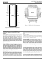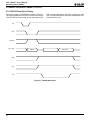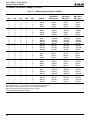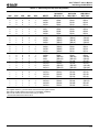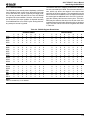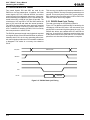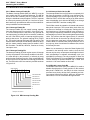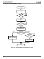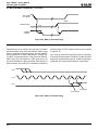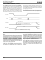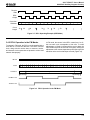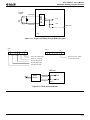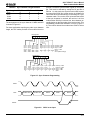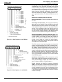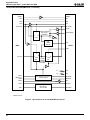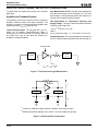
1
SCC™/ESCC™ USER’S MANUAL
TABLE OF CONTENTS
Chapter 1. General Description
1.1 Introduction ....................................................................................................................................
1.2 SCC’s Capabilities .........................................................................................................................
1.3 Block Diagram ...............................................................................................................................
1.4 Pin Descriptions .............................................................................................................................
1.4.1
Pins Common to both Z85X30 and Z80X30 ....................................................................
1.4.2
Pin Descriptions, (Z85X30 Only) ......................................................................................
1.4.3
Pin Descriptions, (Z80X30 Only) ......................................................................................
1-1
1-2
1-4
1-5
1-7
1-8
1-9
Chapter 2. Interfacing the SCC/ESCC
2.1 Introduction .................................................................................................................................... 2-1
2.2 Z80X30 Interface Timing ................................................................................................................ 2-1
2.2.1
Z80X30 Read Cycle Timing ............................................................................................. 2-2
2.2.2
Z80X30 Write Cycle Timing .............................................................................................. 2-3
2.2.3
Z80X30 Interrupt Acknowledge Cycle Timing .................................................................. 2-4
2.2.4
Z80X30 Register Access .................................................................................................. 2-5
2.2.5
Z80C30 Register Enhancement ....................................................................................... 2-8
2.2.6
Z80230 Register Enhancements ...................................................................................... 2-8
2.2.7
Z80X30 Reset .................................................................................................................. 2-9
2.3 Z85X30 Interface Timing ............................................................................................................. 2-10
2.3.1
Z85X30 Read Cycle Timing ........................................................................................... 2-10
2.3.2
Z85X30 Write Cycle Timing ............................................................................................ 2-11
2.3.3
Z85X30 Interrupt Acknowledge Cycle Timing ................................................................ 2-11
2.3.4
Z85X30 Register Access ................................................................................................ 2-12
2.3.5
Z85C30 Register Enhancement ..................................................................................... 2-14
2.3.6
Z85C30/Z85230 Register Enhancements ...................................................................... 2-14
2.3.7
Z85X30 Reset ................................................................................................................ 2-15
2.4 Interface Programming ................................................................................................................ 2-15
2.4.1
I/O Programming Introduction ........................................................................................ 2-15
2.4.2
Polling ............................................................................................................................ 2-16
2.4.3
Interrupts ........................................................................................................................ 2-16
2.4.4
Interrupt Control ............................................................................................................. 2-17
2.4.5
Daisy-Chain Resolution .................................................................................................. 2-19
2.4.6
Interrupt Acknowledge ................................................................................................... 2-21
2.4.7
The Receiver Interrupt ................................................................................................... 2-21
2.4.8
Transmit Interrupts and Transmit Buffer Empty Bit ........................................................ 2-25
2.4.9
External/Status Interrupts ............................................................................................... 2-31
2.5 Block/DMA Transfer ..................................................................................................................... 2-33
2.5.1
Block Transfers .............................................................................................................. 2-33
2.5.2
DMA Requests ............................................................................................................... 2-36
2.6 Test Functions ............................................................................................................................. 2-41
2.6.1
Local Loopback .............................................................................................................. 2-41
2.6.2
Auto Echo ....................................................................................................................... 2-41
i
SCC™/ESCC™ User’s Manual
Table of Contents
Chapter 3. SCC/ESCC Ancillary Support Circuitry
3.1 Introduction .................................................................................................................................... 3-1
3.2 Baud Rate Generator ..................................................................................................................... 3-1
3.3 Data Encoding/Decoding ............................................................................................................... 3-4
3.4 DPLL Digital Phase-Locked Loop .................................................................................................. 3-7
3.4.1
DPLL Operation in the NRZI Mode .................................................................................. 3-8
3.4.2
DPLL Operation in the FM Modes .................................................................................... 3-9
3.4.3
DPLL Operation in the Manchester Mode ...................................................................... 3-10
3.4.4
Transmit Clock Counter (ESCC only) ............................................................................. 3-10
3.5
Clock Selection ........................................................................................................................... 3-11
3.6
Crystal Oscillator ......................................................................................................................... 3-14
Chapter 4. Data Communication Modes
4.1 Introduction .................................................................................................................................... 4-1
4.1.1
Transmit Data Path Description ....................................................................................... 4-1
4.1.2
Receive Data Path Description ....................................................................................... 4-2
4.2 Asynchronous Mode ...................................................................................................................... 4-3
4.2.1
Asynchronous Transmit ................................................................................................... 4-4
4.2.2
Asynchronous Receive .................................................................................................... 4-6
4.2.3
Asynchronous Initialization ............................................................................................... 4-7
4.3 Byte-Oriented Synchronous Mode ................................................................................................. 4-8
4.3.1
Byte-Oriented Synchronous Transmit .............................................................................. 4-8
4.3.2
Byte-Oriented Synchronous Receive ............................................................................. 4-10
4.3.3
Transmitter/Receiver Synchronization ........................................................................... 4-17
4.4 Bit-Oriented Synchronous (SDLC/HDLC) Mode .......................................................................... 4-18
4.4.1
SDLC Transmit ............................................................................................................... 4-19
4.4.2
SDLC Receive ................................................................................................................ 4-22
4.4.3
SDLC Frame Status FIFO .............................................................................................. 4-27
4.4.4
SDLC Loop Mode ........................................................................................................... 4-30
Chapter 5. Register Descriptions
5.1 Introduction .................................................................................................................................... 5-1
5.2 Write Registers .............................................................................................................................. 5-2
5.2.1
Write Register 0 (Command Register) ............................................................................. 5-2
5.2.2
Write Register 1 (Transmit/Receive Interrupt and Data Transfer Mode Definition) .......... 5-4
5.2.3
Write Register 2 (Interrupt Vector) ................................................................................... 5-7
5.2.4
Write Register 3 (Receive Parameters and Control) ........................................................ 5-7
5.2.5
Write Register 4 (Transmit/Receive Miscellaneous Parameters and Modes) .................. 5-8
5.2.6
Write Register 5 (Transmit Parameters and Controls) ..................................................... 5-9
5.2.7
Write Register 6 (Sync Characters or SDLC Address Field) .......................................... 5-10
5.2.8
Write Register 7 (Sync Character or SDLC Flag) ........................................................... 5-11
5.2.9
Write Register 7 Prime (ESCC only) .............................................................................. 5-12
5.2.10 Write Register 7 Prime (85C30 only) .............................................................................. 5-13
5.2.11 Write Register 8 (Transmit Buffer) .................................................................................. 5-13
5.2.12 Write Register 9 (Master Interrupt Control) .................................................................... 5-14
5.2.13 Write Register 10 (Miscellaneous Transmitter/Receiver Control Bits) ........................... 5-15
5.2.14 Write Register 11 (Clock Mode Control) ......................................................................... 5-17
5.2.15 Write Register 12 (Lower Byte of Baud Rate Generator Time Constant) ....................... 5-18
5.2.16 Write Register 13 (Upper Byte of Baud Rate Generator Time Constant) ....................... 5-19
5.2.17 Write Register 14 (Miscellaneous Control Bits) .............................................................. 5-19
5.2.18 Write Register 15 (External/Status Interrupt Control) ..................................................... 5-20
5.3 Read Registers ............................................................................................................................ 5-21
5.3.1
Read Register 0 (Transmit/Receive Buffer Status and External Status) ........................ 5-21
5.3.2
Read Register 1 ............................................................................................................. 5-23
5.3.3
Read Register 2 ............................................................................................................. 5-24
5.3.4
Read Register 3 ............................................................................................................. 5-25
5.3.5
Read Register 4 (ESCC and 85C30 Only) ..................................................................... 5-25
5.3.6
Read Register 5 (ESCC and 85C30 Only) ..................................................................... 5-25
ii
SCC™/ESCC™ User’s Manual
Table of Contents
5.3.7
5.3.8
5.3.9
5.3.10
5.3.11
5.3.12
5.3.13
5.3.14
5.3.15
5.3.16
Read Register 6 (Not on NMOS) ...................................................................................
Read Register 7 (Not on NMOS) ...................................................................................
Read Register 8 .............................................................................................................
Read Register 9 (ESCC and 85C30 Only) .....................................................................
Read Register 10 ...........................................................................................................
Read Register 11 (ESCC and 85C30 Only) ...................................................................
Read Register 12 ...........................................................................................................
Read Register 13 ...........................................................................................................
Read Register 14 (ESCC and 85C30 Only) ...................................................................
Read Register 15 ...........................................................................................................
5-25
5-25
5-26
5-26
5-26
5-27
5-27
5-27
5-27
5-27
Chapter 6. Application Notes
Interfacing Z80® CPUs to the Z8500 Peripheral Family ......................................................................... 6-1
The Z180™ Interfaced with the SCC at MHZ........................................................................................ 6-34
The Zilog Datacom Family with the 80186 CPU .................................................................................. 6-59
SCC in Binary Synchronous Communications ...................................................................................... 6-79
Serial Communication Controller (SCC™): SDLC Mode of Operation .................................................. 6-93
Using SCC with Z8000 in SDLC Protocol6-105
Boost Your System Performance Using The Zilog ESCC™ ................................................................ 6-117
Technical Considerations When Implementing LocalTalk Link Access Protocol ................................ 6-131
On-Chip Oscillator Design................................................................................................................... 6-151
Chapter 7. Questions and Answers
Zilog SCC Z8030/Z8530 Questions and Answers................................................................................... 7-1
Zilog ESCC™ Controller Questions and Answers ................................................................................. 7-11
iii
USER’S MANUAL
1
CHAPTER 1
GENERAL DESCRIPTION
1.1 INTRODUCTION
The Zilog SCC Serial Communication Controller is a dual
channel, multiprotocol data communication peripheral designed for use with 8- and 16-bit microprocessors. The
SCC functions as a serial-to-parallel, parallel-to-serial converter/controller. The SCC can be software-configured to
satisfy a wide variety of serial communications applications. The device contains a variety of new, sophisticated
internal functions including on-chip baud rate generators,
digital phase-lock loops, and crystal oscillators, which dramatically reduce the need for external logic.
The SCC handles asynchronous formats, synchronous
byte-oriented protocols such as IBM® Bisync, and synchronous bit-oriented protocols such as HDLC and IBM
SDLC. This versatile device supports virtually any serial
data transfer application (telecommunication, LAN, etc.)
The device can generate and check CRC codes in any
synchronous mode and can be programmed to check data
integrity in various modes. The SCC also has facilities for
modem control in both channels. In applications where
these controls are not needed, the modem controls can be
used for general-purpose I/O.
With access to 14 Write registers and 7 Read registers per
channel (the number of the registers varies depending on
the version), the user can configure the SCC to handle all
synchronous formats regardless of data size, number of
stop bits, or parity requirements.
Within each operating mode, the SCC also allows for protocol variations by checking odd or even parity bits, character insertion or deletion, CRC generation, checking
break and abort generation and detection, and many other
protocol-dependent features.
The SCC/ESCC family consists of the following seven
devices;
NMOS
CMOS
ESCC
EMSCC
Z-Bus®
Universal-Bus
Z8030
Z80C30
Z80230
Z8530
Z85C30
Z85230
Z85233
As a convention, use the following words to distinguish the
devices throughout this document.
SCC: Description applies to all versions.
NMOS: Description applies to NMOS version
(Z8030/Z8530)
CMOS: Description applies to CMOS version
(Z80C30/Z85C30)
ESCC: Description applies to ESCC
(Z80230/Z85230)
EMSCC: Description applies to EMSCC (Z85233)
Z80X30: Description applies to Z-Bus version of the
device (Z8030/Z80C30/Z80230)
Z85X3X: Description applies to Universal version of
the device (Z8530/Z85C30/Z85230/Z85233)
The Z-Bus version has a multiplexed bus interface and is
directly compatible with the Z8000, Z16C00 and 80x86
CPUs. The Universal version has a non-multiplexed bus
interface and easily interfaces with virtually any CPU, including the 8080, Z80, 68X00.
1-1
SCC™/ESCC™ User’s Manual
General Description
1.2 SCC’S CAPABILITIES
The NMOS version of the SCC is Zilog’s original device.
The design is based on the Z80 SIO architecture. If you are
familiar with the Z80 SIO, the SCC can be treated as an
SIO with support circuitry such as DPLL, BRG, etc. Its features include:
■
■
■
Two independent full-duplex channels
■
Synchronous/Isosynchronous data rates:
– Up to 1/4 of the PCLK using external clock source.
Up to 5 Mbits/sec at 20 MHz PCLK (ESCC)
Up to 4 Mbits/sec at 16 MHz PCLK (CMOS)
Up to 2 MBits/sec at 8 MHz PCLK (NMOS)
– Up to 1/8 of the PCLK (up to 1/16 on NMOS) using
FM encoding with DPLL
– Up to 1/16 of the PCLK (up to 1/32 on NMOS)
using NRZI encoding with DPLL
■
■
■
1-2
Asynchronous Capabilities
– 5, 6, 7 or 8 bits/character (capable of handling 4
bits/character or less.)
– 1, 1.5, or 2 stop bits
– Odd or even parity
– Times 1, 16, 32 or 64 clock modes
– Break generation and detection
– Parity, overrun and framing error detection
Byte oriented synchronous capabilities:
– Internal or external character synchronization
– One or two sync characters (6 or 8 bits/sync
character) in separate registers
– Automatic Cyclic Redundancy Check (CRC)
generation/detection
SDLC/HDLC capabilities:
– Abort sequence generation and checking
– Automatic zero insertion and detection
– Automatic flag insertion between messages
– Address field recognition
– I-field residue handling
– CRC generation/detection
– SDLC loop mode with EOP recognition/loop entry
and exit
Receiver FIFO
ESCC:
8 bytes deep
NMOS/CMOS:
3 bytes deep
Transmitter FIFO
ESCC:
4 bytes deep
NMOS/CMOS:
1 byte deep
■
NRZ, NRZI or FM encoding/decoding. Manchester code
decoding (encoding with external logic).
■
Baud Rate Generator in each channel
■
Digital Phase Locked Loop (DPLL) for clock recovery
■
Crystal oscillator
The CMOS version of the SCC is 100% plug in compatible
to the NMOS versions of the device, while providing the
following additional features:
■
Status FIFO
■
Software interrupt acknowledge feature
■
Enhanced timing specifications
■
Faster system clock speed
■
Designed in Zilog’s Superintegration™ core format
■
When the DPLL clock source is external, it can be up to
2x the PCLK, where NMOS allows up to PCLK (32.3
MHz max with 16/20 MHz version).
SCC™/ESCC™ User’s Manual
General Description
The Z85C30 CMOS SCC has added new features, while
maintaining 100% hardware/software compatibility. It has
the following new features:
ESCC (Enhanced SCC) is pin and software compatible to the CMOS version, with the following additional
enhancements.
■
New programmable WR7' (write register 7 prime) to
enable new features.
■
Deeper transmit FIFO (4 bytes)
■
Deeper receive FIFO (8 bytes)
■
Improvements to support SDLC mode of synchronous
communication:
– Improved functionality to ease sending back-to
back frames
– Automatic SDLC opening Flag transmission*
– Automatic Tx Underrun/EOM Latch reset in SDLC
mode*
– Automatic /RTS deactivation*
– TxD pin forced “H” in SDLC NRZI mode after
closing flag*
– Complete CRC reception*
– Improved response to Abort sequence in status
FIFO
– Automatic Tx CRC generator preset/reset
– Extended read for write registers*
– Write data setup timing improvement
■
Programmable FIFO interrupt and DMA request level
■
Seven enhancements to improve SDLC link layer
supports:
– Automatic transmission of the opening flag
– Automatic reset of Tx Underrun/EOM latch
– Deactivation of /RTS pin after closing flag
– Automatic CRC generator preset
– Complete CRC reception
– TxD pin automatically forced high with NRZI
encoding when using mark idle
– Status FIFO handles better frames with an
ABORT
– Receive FIFO automatically unlocked for special
receive interrupts when using the SDLC status
FIFO
Improved AC timing:
– Three to 3.5 PCLK access recovery time.
– Programmable /DTR//REQ timing*
– Elimination of write data to falling edge of /WR
setup time requirement
– Reduced /INT timing
■
Delayed bus latching for easier microprocessor
interface
■
New programmable features added with Write Register
7' (WR seven prime)
■
Write registers 3, 4, 5 and 10 are now readable
Other features include:
– Extended read function to read back the written
value to the write registers*
– Latching RR0 during read
– RR0, bit D7 and RR10, bit D6 now has reset
defaultvalue.
Some of the features listed above are available by default, and some of them (features with “*”) are disabled on
default.
■
Read register 0 latched during access
■
DPLL counter output available as jitter-free transmitter
clock source
■
Enhanced /DTR, /RTS deactivation timing
■
■
1-3
1
SCC™/ESCC™ User’s Manual
General Description
1.3 BLOCK DIAGRAM
Figure 1-1 has the block diagram of the SCC. Note that the
depth of the FIFO differs depending on the version. The
10X19 SDLC Frame Status FIFO is not available on the
NMOS version of the SCC.
Detailed internal signal path will be discussed in Chapter 4.
Transmit Log
Transmit FIFO
NMOS/CMOS: 1 by
Transmit MU
ESCC: 4 Bytes
TxDA
Data Encoding & CR
Generation
Channel A
Receive and Transmit Clock Mult
Exploded Vie
/TRxCA
/RTxCA
Digital
Phase-Locke
Loop
Crystal
Oscillato
Amplifie
Baud Rate
Generato
Modem/Control Lo
/CTSA
/DCDA
/SYNCA
/RTSA
/DTRA//REQ
Receive Log
Rec. Status*Rec. Data*
FIFO
FIFO
Receive MU
SDLC Frame Status F
10 x 19
CRC Checker
Data Decode &
Sync Charact
Detection
RxDA
** See No
* NMOS/CMOS: 3 bytes each
ESCC: 8 bytes
** Not Available on NMOS
Databus
Interna
Contro
Logic
Channel A
Register
Interrup
Control
Logic
Channel B
Register
Channel A
CPU & DMA
Bus Interfac
Contro
Interru
Contro
/INT
/INTAC
IEI
IEO
Figure 1-1. SCC Block Diagram
1-4
Channel B
SCC™/ESCC™ User’s Manual
General Description
1.4 PIN DESCRIPTIONS
The SCC pins are divided into seven functional groups:
Address/Data, Bus Timing and Reset, Device Control, Interrupt, Serial Data (both channels), Peripheral Control
(both channels), and Clocks (both channels). Figures 1-2
and 1-3 show the pins in each functional group for both
Z80X30 and Z85X30. Notice the pin functions unique to
each bus interface version in the Address/Data group, Bus
Timing and Reset group, and Control groups.
The timing and control groups designate the type of transaction to occur and when it will occur. The interrupt group
provides inputs and outputs to conform to the Z-Bus®
specifications for handling and prioritizing interrupts. The
remaining groups are divided into channel A and channel
B groups for serial data (transmit or receive), peripheral
control (such as DMA or modem), and the input and output
lines for the receive and transmit clocks.
The Address/Data group consists of the bidirectional lines
used to transfer data between the CPU and the SCC (Addresses in the Z80X30 are latched by /AS). The direction
of these lines depends on whether the operation is a Read
or Write.
The signal functionality and pin assignments (Figures 1-4
to 1-7) stay constant within the same bus interface group
(i.e., Z80X30, Z85X30), except for some timing and/or DC
specification differences. For details, please reference the
individual product specifications.
Data Bus
Bus Timing
and Reset
Control
Interrupt
D7
TxDA
D6
RxDA
D5
/TRxCA
D4
/RTxCA
D3
/SYNCA
D2
/W//REQA
D1
/DTR//REQA
D0
/RTSA
/RD
/CTSA
/WR
Z85X30 /DCDA
A//B
TxDB
/CE
RxDB
D//C
/TRxCB
/INT
/RTxCB
/INTACK
/SYNCB
IEI
IEO
/W//REQB
/DTR//REQB
/RTSB
/CTSB
Serial
Data
Channel
Clocks
Channel
Controls
for Modem,
DMA and
Other
Serial
Data
Channel
Clocks
Channel
Controls
for Modem,
DMA and
Other
/DCDB
Figure 1-2. Z85X30 Pin Functions
1-5
1
SCC™/ESCC™ User’s Manual
General Description
1.4 PIN DESCRIPTIONS (Continued)
Address
Data Bus
Bus Timing
and Reset
Control
Interrupt
AD7
TxDA
AD6
RxDA
AD5
/TRxCA
AD4
/RTxCA
AD3
/SYNCA
AD2
/W//REQA
AD1
/DTR//REQA
AD0
/RTSA
/AS
/CTSA
/DS
/DCDA
Z80X30
R//W
TxDB
CS1
RxDB
/CS0
/TRxCB
/INT
/RTxCB
/INTACK
/SYNCB
IEI
IEO
Serial
Data
Channel
Clocks
Channel A
Channel
Controls
for Modem,
DMA and
Other
Serial
Data
Channel
Clocks
Channel B
/W//REQB
Channel
Controls
for Modem,
DMA and
Other
/DTR//REQB
/RTSB
/CTSB
/DCDB
Figure 1-3. Z80X30 Pin Functions
D1
1
40
D0
D3
2
39
D2
D5
3
38
D4
D7
4
37
D6
/INT
5
36
/RD
IEO
6
35
/WR
IEI
7
34
A//B
/INTACK
8
33
/CE
VCC
9
32
D//C
10
31
GND
/W//REQB
/W//REQA
Z85X30
/SYNCA
11
30
/RTxCA
12
29
/SYNCB
RxDA
13
28
/RTxCB
/TRxCA
14
27
RxDB
TxDA
15
26
/TRxCB
16
25
TxDB
/RTSA
17
24
/DTR//REQB
/CTSA
18
23
RTSB
/DCDA
19
22
/CTSB
PCLK
20
21
/DCDB
/DTR//REQA
Figure 1-4. Z85X30 DIP Pin Assignments
1-6
Figure 1-5. Z85X30 PLCC Pin Assignments
SCC™/ESCC™ User’s Manual
General Description
AD1
1
40
AD0
AD3
2
39
AD2
AD5
3
38
AD4
AD7
4
37
AD6
/INT
5
36
/DS
IEO
6
35
/AS
IEI
7
34
R//W
/INTACK
8
33
/CS0
VCC
9
32
CS1
/W//REQA
10
31
GND
/SYNCA
11
30
/W//REQB
/RTxCA
12
29
/SYNCB
RxDA
13
28
/RTxCB
/TRxCA
14
27
RxDB
TxDA
15
26
/TRxCB
16
25
TxDB
/RTSA
17
24
/DTR//REQB
/CTSA
18
23
RTSB
/DCDA
19
22
/CTSB
PCLK
20
21
/DCDB
/DTR//REQA
Z80X30
1
Figure 1-7. Z80X30 PLCC Pin Assignments
Figure 1-6. Z80X30 DIP Pin Assignments
1.4.1 Pins Common to both Z85X30 and
Z80X30
outputs, and, they strictly follow the inverse state of WR5,
bit D1.
/CTSA, /CTSB. Clear To Send (inputs, active Low). These
pins function as transmitter enables if they are programmed for Auto Enable (WR3, D5=1). A Low on the inputs enables the respective transmitters. If not programmed as Auto Enable, they may be used as generalpurpose inputs. Both inputs are Schmitt-trigger buffered to
accommodate slow rise-time inputs. The SCC detects
pulses on these inputs and can interrupt the CPU on both
logic level transitions.
ESCC and 85C30:
In SDLC mode, the /RTS pins can be programmed to
be deasserted when the closing flag of the message
clears the TxD pin, if WR7' D2 is set.
/DCDA, /DCDB. Data Carrier Detect (inputs, active Low).
These pins function as receiver enables if they are programmed for Auto Enable (WR3, D5=1); otherwise, they
are used as general-purpose input pins. Both pins are
Schmitt-trigger buffered to accommodate slow rise time
signals. The SCC detects pulses on these pins and can interrupt the CPU on both logic level transitions.
/RTSA, /RTSB. Request To Send (outputs, active Low).
The /RTS pins can be used as general-purpose outputs or
with the Auto Enable feature. When used with Auto Enable
ON (WR3, D5=1) in asynchronous mode, the /RTS pin
goes High after the transmitter is empty. When Auto Enable is OFF, the /RTS pins are used as general-purpose
/SYNCA, /SYNCB. Synchronization (inputs or outputs, active Low). These pins can act either as inputs, outputs, or
part of the crystal oscillator circuit. In the Asynchronous
Receive mode (crystal oscillator option not selected),
these pins are inputs similar to CTS and DCD. In this
mode, transitions on these lines affect the state of the Synchronous/Hunt status bits in Read Register 0 but have no
other function.
In External Synchronization mode, with the crystal oscillator not selected, these lines also act as inputs. In this
mode, /SYNC is driven Low to receive clock cycles after
the last bit in the synchronous character is received. Character assembly begins on the rising edge of the receive
clock immediately preceding the activation of SYNC.
In the Internal Synchronization mode (Monosync and Bisync) with the crystal oscillator not selected, these pins
act as outputs and are active only during the part of the
1-7
SCC™/ESCC™ User’s Manual
General Description
1.4 PIN DESCRIPTIONS (Continued)
receive clock cycle in which the synchronous condition is
not latched. These outputs are active each time a synchronization pattern is recognized (regardless of character
boundaries). In SDLC mode, the pins act as outputs and
are valid on receipt of a flag. The /SYNC pins switch from
input to output when monosync, bisync, or SDLC is programmed in WR4 and sync modes are enabled.
/DTR//REQA, /DTR//REQB. Data Terminal Ready/Request (outputs, active Low). These pins are programmable
(WR14, D2) to serve either as general-purpose outputs or
as DMA Request lines. When programmed for DTR function (WR14 D2=0), these outputs follow the state programmed into the DTR bit of Write Register 5 (WR5 D7).
When programmed for Ready mode, these pins serve as
DMA Requests for the transmitter.
ESCC and 85C30:
When used as DMA request lines (WR14, D2=1), the
timing for the deactivation request can be programmed in the added register, Write Register 7'
(WR7') bit D4. If this bit is set, the /DTR//REQ pin is deactivated with the same timing as the /W/REQ pin. If
WR7' D4 is reset, the deactivation timing of /DTR//REQ
pin is four clock cycles, the same as in the Z85C30.
/W//REQA, /W//REQB. Wait/Request (outputs, open-drain
when programmed for Wait function, driven High or Low
when programmed for Ready function). These dual-purpose outputs may be programmed as Request lines for a
DMA controller or as Wait lines to synchronize the CPU to
the SCC data rate. The reset state is Wait.
RxDA, RxDB. Receive Data (inputs, active High). These
input signals receive serial data at standard TTL levels.
/RTxCA, /RTxCB. Receive/Transmit Clocks (inputs, active
Low). These pins can be programmed to several modes of
operation. In each channel, /RTxC may supply the receive
clock, the transmit clock, the clock for the baud rate generator, or the clock for the Digital Phase-Locked Loop. These
pins can also be programmed for use with the respective
SYNC pins as a crystal oscillator. The receive clock may
be 1, 16, 32, or 64 times the data rate in asynchronous
modes.
TxDA, TxDB. Transmit Data (outputs, active High). These
output signals transmit serial data at standard TTL levels.
/TRxCA, /TRxCB. Transmit/Receive Clocks (inputs or outputs, active Low). These pins can be programmed in several different modes of operation. /TRxC may supply the
receive clock or the transmit clock in the input mode or
supply the output of the Transmit Clock Counter (which
1-8
parallels the Digital Phase-Locked Loop), the crystal oscillator, the baud rate generator, or the transmit clock in the
output mode.
PCLK. Clock (input). This is the master SCC clock used to
synchronize internal signals. PCLK is a TTL level signal.
PCLK is not required to have any phase relationship with
the master system clock.
IEI. Interrupt Enable In (input, active High). IEI is used with
IEO to form an interrupt daisy chain when there is more
than one interrupt driven device. A high IEI indicates that
no other higher priority device has an interrupt under service or is requesting an interrupt.
IEO. Interrupt Enable Out (output, active High). IEO is High
only if IEI is High and the CPU is not servicing the SCC interrupt or the SCC is not requesting an interrupt (Interrupt
Acknowledge cycle only). IEO is connected to the next
lower priority device’s IEI input and thus inhibits interrupts
from lower priority devices.
/INT. Interrupt (output, open drain, active Low). This signal
is activated when the SCC requests an interrupt. Note that
/INT is an open-drain output.
/INTACK. Interrupt Acknowledge (input, active Low). This
is a strobe which indicates that an interrupt acknowledge
cycle is in progress. During this cycle, the SCC interrupt
daisy chain is resolved. The device is capable of returning
an interrupt vector that may be encoded with the type of interrupt pending. During the acknowledge cycle, if IEI is
high, the SCC places the interrupt vector on the databus
when /RD goes active. /INTACK is latched by the rising
edge of PCLK.
1.4.2 Pin Descriptions, (Z85X30 Only)
D7-D0. Data bus (bidirectional, tri-state). These lines carry
data and commands to and from the Z85X30.
/CE. Chip Enable (input, active Low). This signal selects
the Z85X30 for a read or write operation.
/RD. Read (input, active Low). This signal indicates a read
operation and when the Z85X30 is selected, enables the
Z85X30’s bus drivers. During the Interrupt Acknowledge cycle, /RD gates the interrupt vector onto the bus if the Z85X30
is the highest priority device requesting an interrupt.
/WR. Write (input, active Low). When the Z85X30 is selected, this signal indicates a write operation. This indicates
that the CPU wants to write command bytes or data to the
Z85X30 write registers.
SCC™/ESCC™ User’s Manual
General Description
A//B. Channel A/Channel B (input). This signal selects the
channel in which the read or write operation occurs. High
selects channel A and Low selects channel B.
/CS0. Chip Select 0 (input, active Low). This signal is
latched concurrently with the addresses on AD7-AD0 and
must be active for the intended bus transaction to occur.
D//C. Data/Control Select (input). This signal defines the
type of information transferred to or from the Z85X30.
High means data is being transferred and Low indicates
a command.
CS1. Chip Select 1 (input, active High). This second select
signal must also be active before the intended bus transaction can occur. CS1 must remain active throughout the
transaction.
1.4.3 Pin Descriptions, (Z80X30 Only)
/DS. Data Strobe (input, active Low). This signal provides
timing for the transfer of data into and out of the Z80X30.
If /AS and /DS are both Low, this is interpreted as a reset.
AD7-AD0. Address/Data Bus (bidirectional, active High,
tri-state). These multiplexed lines carry register addresses
to the Z80X30 as well as data or control information to and
from the Z80X30.
/AS. Address Strobe (input, active Low). Address on AD7AD0 are latched by the rising edge of this signal.
R//W. Read//Write (input, read active High). This signal
specifies whether the operation to be performed is a read
or a write.
© 1998 by Zilog, Inc. All rights reserved. No part of this
document may be copied or reproduced in any form or by
any means without the prior written consent of Zilog, Inc.
The information in this document is subject to change
without notice. Devices sold by Zilog, Inc. are covered by
warranty and patent indemnification provisions appearing
in Zilog, Inc. Terms and Conditions of Sale only.
ZILOG, INC. MAKES NO WARRANTY, EXPRESS,
STATUTORY, IMPLIED OR BY DESCRIPTION,
REGARDING THE INFORMATION SET FORTH HEREIN
OR REGARDING THE FREEDOM OF THE DESCRIBED
DEVICES
FROM
INTELLECTUAL
PROPERTY
INFRINGEMENT. ZILOG, INC. MAKES NO WARRANTY
OF MERCHANTABILITY OR FITNESS FOR ANY
PURPOSE.
Zilog, Inc. shall not be responsible for any errors that may
appear in this document. Zilog, Inc. makes no commitment
to update or keep current the information contained in this
document.
Zilog’s products are not authorized for use as critical
components in life support devices or systems unless a
specific written agreement pertaining to such intended use
is executed between the customer and Zilog prior to use.
Life support devices or systems are those which are
intended for surgical implantation into the body, or which
sustains life whose failure to perform, when properly used
in accordance with instructions for use provided in the
labeling, can be reasonably expected to result in
significant injury to the user.
Zilog, Inc. 210 East Hacienda Ave.
Campbell, CA 95008-6600
Telephone (408) 370-8000
FAX 408 370-8056
Internet: http://www.zilog.com
1-9
1
USER’S MANUAL
2
CHAPTER 2
INTERFACING THE SCC/ESCC
2.1 INTRODUCTION
This chapter covers the system interface requirements
with the SCC. Timing requirements for both devices are
described in a general sense here, and the user should refer to the SCC Product Specification for detailed AC/DC
parametric requirements.
The ESCC and the 85C30 have an additional register,
Write Register Seven Prime (WR7'). Its features include
the ability to read WR3, WR4, WR5, WR7', and WR10.
Both the ESCC and the 85C30 have the ability to deassert
the /DTR//REG pin quickly to ease DMA interface design.
Additionally, the Z85230 features a relaxed requirement for
a valid data bus when the /WR pin goes Low. The effects
of the deeper data FIFOs should be considered when writing the interrupt service routines. The user should read the
sections which follow for details on these features.
2.2 Z80X30 INTERFACE TIMING
The Z-Bus® compatible SCC is suited for system applications with multiplexed address/data buses similar to the
Z8®, Z8000®, and Z280®.
Two control signals, /AS and /DS, are used by the Z80X30
to time bus transactions. In addition, four other control signals (/CS0, CS1, R//W, and /INTACK) are used to control
the type of bus transaction that occurs. A bus transaction
is initiated by /AS; the rising edge latches the register address on the Address/Data bus and the state of /INTACK
and /CS0.
In addition to timing bus transactions, /AS is used by the
interrupt section to set the Interrupt Pending (IP) bits.
Because of this, /AS must be kept cycling for the interrupt section to function properly.
The Z80X30 generates internal control signals in response
to a register access. Since /AS and /DS have no phase relationship with PCLK, the circuit generating these internal
control signals provides time for metastable conditions to
disappear. This results in a recovery time related to PCLK.
This recovery time applies only to transactions involving
the Z80X30, and any intervening transactions are ignored.
This recovery time is four PCLK cycles, measured from the
falling edge of /DS of one access to the SCC, to the falling
edge of /DS for a subsequent access.
2-1
SCC™/ESCC™ User’s Manual
Interfacing the SCC/ESCC
2.2 Z80X30 INTERFACE TIMING (Continued)
2.2.1 Z80X30 Read Cycle Timing
The read cycle timing for the Z80X30 is shown in Figure 2-1.
The register address on AD7-AD0, as well as the state of
/CS0 and /INTACK, are latched by the rising edge of /AS.
R//W must be High before /DS falls to indicate a read
cycle. The Z80X30 data bus drivers are enabled while CS1
is High and /DS is Low.
/AS
/CS0
/INTACK
AD7 - AD0
Address
R//W
CS1
/DS
Figure 2-1. Z80X30 Read Cycle
2-2
Data Valid
SCC™/ESCC™ User’s Manual
Interfacing the SCC/ESCC
2.2.2 Z80X30 Write Cycle Timing
The write cycle timing for the Z80X30 is shown in
Figure 2-2. The register address on AD7-AD0, as well as
the state of /CS0 and /INTACK, are latched by the rising
edge of /AS. R//W must be Low when /DS falls to indicate
a write cycle. The leading edge of the coincidence of CS1
High and /DS Low latches the write data on AD7-AD0, as
well as the state of R//W.
/AS
/CS0
/INTACK
AD7 - AD0
Address
Data Valid
R//W
CS1
/DS
Figure 2-2. Z80X30 Write Cycle
2-3
2
SCC™/ESCC™ User’s Manual
Interfacing the SCC/ESCC
2.2 Z80X30 INTERFACE TIMING (Continued)
2.2.3 Z80X30 Interrupt Acknowledge Cycle Timing
The interrupt acknowledge cycle timing for the Z80X30 is
shown in Figure 2-3. The address on AD7-AD0 and the
state of /CS0 and /INTACK are latched by the rising edge
of /AS. However, if /INTACK is Low, the address, /CS0,
CS1 and R//W are ignored for the duration of the interrupt
acknowledge cycle.
/AS
/CS0
Vector
AD7 - AD0
/DS
/INTACK
IEI
IEO
/INT
Figure 2-3. Z80X30 Interrupt Acknowledge Cycle
2-4
SCC™/ESCC™ User’s Manual
Interfacing the SCC/ESCC
The Z80X30 samples the state of /INTACK on the rising
edge of /AS, and AC parameters #7 and #8 specify the setup and hold-time requirements. Between the rising edge of
/AS and the falling edge of /DS, the internal and external
daisy chains settle (AC parameter #29). A system with no
external daisy chain should provide the time specified in
spec #29 to settle the interrupt daisy-chain priority internal
to the SCC. Systems using an external daisy chain should
refer to Note 5 referenced in the Z80X30 Read/Write & Interrupt Acknowledge Timing for the time required to settle
the daisy chain.
Shift Right/Shift Left bit in the Channel B WR0 controls
which bits are decoded to form the register address. It is
placed in this register to simplify programming when the
current state of the Shift Right/Shift Left bit is not known.
Note: /INTACK is sampled on the rising edge of /AS. If it
does not meet the setup time to the first rising edge of /AS
of the interrupt acknowledge cycle, it is latched on the next
rising edge of /AS. Therefore, if /INTACK is asynchronous
to /AS, it may be necessary to add a PCLK cycle to the calculation for /INTACK to /RD delay time.
While in the Shift Left mode, the register address is
placed on AD4-AD1 and the Channel Select bit, A/B, is
decoded from AD5. The register map for this case is
shown in Table 2-1. In Shift Right mode, the register address is again placed on AD4-AD1 but the channel select
A/B is decoded from AD0. The register map for this case
is shown in Table 2-2.
If there is an interrupt pending in the SCC, and IEI is High
when /DS falls, the acknowledge cycle was intended for
the SCC. This being the case, the Z80X30 sets the Interrupt-Under-Service (IUS) latch for the highest priority
pending interrupt, as well as placing an interrupt vector on
AD7-AD0. The placing of a vector on the bus can be disabled by setting WR9, D1=1. The /INT pin also goes inactive in response to the falling edge of /DS. Note that there
should be only one /DS per acknowledge cycle. Another
important fact is that the IP bits in the Z80X30 are updated
by /AS, which may delay interrupt requests if the processor
does not supply /AS strobes during the time between accesses of the Z80X30.
2.2.4 Z80X30 Register Access
The registers in the Z80X30 are addressed via the address
on AD7-AD0 and are latched by the rising edge of /AS. The
A hardware reset forces Shift Left mode where the address
is decoded from AD5-AD1. In Shift Right mode, the address is decoded from AD4-AD0. The Shift Right/Shift Left
bit is written via a command to make the software writing
to WR0 independent of the state of the Shift Right/Shift
Left bit.
Because the Z80X30 does not contain 16 read registers,
the decoding of the read registers is not complete; this is
indicated in Table 2-1 and Table 2-2 by parentheses
around the register name. These addresses may also be
used to access the read registers. Also, note that the
Z80X30 contains only one WR2 and WR9; these registers
may be written from either channel.
Shift Left Mode is used when Channel A and B are to be
programmed differently. This allows the software to sequence through the registers of one channel at a time. The
Shift Right Mode is used when the channels are programmed the same. By incrementing the address, the user
can program the same data value into both the Channel A
and Channel B register.
2-5
2
SCC™/ESCC™ User’s Manual
Interfacing the SCC/ESCC
2.2 Z80X30 INTERFACE TIMING (Continued)
Table 2-1. Z80X30 Register Map (Shift Left Mode)
AD5
0
0
0
0
0
0
0
0
0
0
0
0
0
0
0
0
1
1
1
1
1
1
1
1
1
1
1
1
1
1
1
1
AD4
0
0
0
0
0
0
0
0
1
1
1
1
1
1
1
1
0
0
0
0
0
0
0
0
1
1
1
1
1
1
1
1
AD3
0
0
0
0
1
1
1
1
0
0
0
0
1
1
1
1
0
0
0
0
1
1
1
1
0
0
0
0
1
1
1
1
AD2
0
0
1
1
0
0
1
1
0
0
1
1
0
0
1
1
0
0
1
1
0
0
1
1
0
0
1
1
0
0
1
1
AD1
0
1
0
1
0
1
0
1
0
1
0
1
0
1
0
1
0
1
0
1
0
1
0
1
0
1
0
1
0
1
0
1
WRITE
WR0B
WR1B
WR2
WR3B
WR4B
WR5B
WR6B
WR7B
WR8B
WR9
WR10B
WR11B
WR12B
WR13B
WR14B
WR15B
WR0A
WR1A
WR2
WR3A
WR4A
WR5A
WR6A
WR7A
WR8A
WR9
WR10A
WR11A
WR12A
WR13A
WR14A
WR15A
READ 8030
80C30/230*
WR15 D2 = 0
RR0B
RR1B
RR2B
RR3B
(RR0B)
(RR1B)
(RR2B)
(RR3B)
RR8B
(RR13B)
RR10B
(RR15B)
RR12B
RR13B
RR14B
RR15B
RR0A
RR1A
RR2A
RR3A
(RR0A)
(RR1A)
(RR2A)
(RR3A)
RR8A
(RR13A)
RR10A
(RR15A)
RR12A
RR13A
RR14A
RR15A
Notes:
The register names in ( ) are the values read out from that register location.
WR15, bit D2 enables status FIFO function (not available on NMOS).
WR7' bit D6 enables extend read function (only on ESCC).
* Includes 80C30/230 when WR15 D2=0.
2-6
80C30/230
WR15 D2=1
RR0B
RR1B
RR2B
RR3B
(RR0B)
(RR1B)
RR6B
RR7B
RR8B
(RR13B)
RR10B
(RR15B)
RR12B
RR13B
RR14B
RR15B
RR0A
RR1A
RR2A
RR3A
(RR0A)
(RR1A)
RR6A
RR7A
RR8A
(RR13A)
RR10A
(RR15A)
RR12A
RR13A
RR14A
RR15A
80230
WR15 D2=1
WR7' D6=1
RR0B
RR1B
RR2B
RR3B
(WR4B)
(WR5B)
RR6B
RR7B
RR8B
(WR3B)
RR10B
(WR10B)
RR12B
RR13B
(WR7’B)
RR15B
RR0A
RR1A
RR2A
RR3A
(WR4A)
(WR5A)
RR6A
RR7A
RR8A
(WR3A)
RR10A
(WR10A)
RR12A
RR13A
(WR7’A)
RR15A
SCC™/ESCC™ User’s Manual
Interfacing the SCC/ESCC
Table 2-2. Z80X30 Register Map (Shift Right Mode)
AD4
0
0
0
0
0
0
0
0
0
0
0
0
0
0
0
0
1
1
1
1
1
1
1
1
1
1
1
1
1
1
1
1
AD3
0
0
0
0
0
0
0
0
1
1
1
1
1
1
1
1
0
0
0
0
0
0
0
0
1
1
1
1
1
1
1
1
AD2
0
0
0
0
1
1
1
1
0
0
0
0
1
1
1
1
0
0
0
0
1
1
1
1
0
0
0
0
1
1
1
1
AD1
0
0
1
1
0
0
1
1
0
0
1
1
0
0
1
1
0
0
1
1
0
0
1
1
0
0
1
1
0
0
1
1
AD0
0
1
0
1
0
1
0
1
0
1
0
1
0
1
0
1
0
1
0
1
0
1
0
1
0
1
0
1
0
1
0
1
WRITE
WR0B
WR0A
WR1B
WR1A
WR2
WR2
WR3B
WR3A
WR4B
WR4A
WR5B
WR5A
WR6B
WR6A
WR7B
WR7A
WR8B
WR8A
WR9
WR9
WR10B
WR10A
WR11B
WR11A
WR12B
WR12A
WR13B
WR13A
WR14B
WR14A
WR15B
WR15A
READ 8030
80C30/230*
WR15 D2 = 0
RR0B
RR0A
RR1B
RR1A
RR2B
RR2A
RR3B
RR3A
(RR0B)
(RR0A)
(RR1B)
(RR1A)
(RR2B)
(RR2A)
(RR3B)
(RR3A)
RR8B
RR8A
(RR13B)
(RR13A)
RR10B
RR10A
(RR15B)
(RR15A)
RR12B
RR12A
RR13B
RR13A
RR14B
RR14A
RR15B
RR15A
80C30/230
WR15 D2=1
RR0B
RR0A
RR1B
RR1A
RR2B
RR2A
RR3B
RR3A
(RR0B)
(RR0A)
(RR1B)
(RR1A)
RR6B
RR6A
RR7B
RR7A
RR8B
RR8A
(RR13B)
(RR13A)
RR10B
RR10A
(RR15B)
(RR15A)
RR12B
RR12A
RR13B
RR13A
RR14B
RR14A
RR15B
RR15A
80230
WR15 D2=1
WR7' D6=1
RR0B
RR0A
RR1B
RR1A
RR2B
RR2A
RR3B
RR3A
(WR4B)
(WR4A)
(WR5B)
(WR5A)
RR6B
RR6A
RR7B
RR7A
RR8B
RR8A
(WR3B)
(WR3A)
RR10B
RR10A
(WR10B)
(WR10A)
RR12B
RR12A
RR13B
RR13A
(WR7’B)
(WR7’A)
RR15B
RR15A
Notes:
The register names in ( ) are the values read out from that register location.
WR15 bit D2 enables status FIFO function (not available on NMOS).
WR7' bit D6 enables extend read function (only on ESCC).
* Includes 80C30/230 when WR15 D2=0.
2-7
2
SCC™/ESCC™ User’s Manual
Interfacing the SCC/ESCC
2.2 Z80X30 INTERFACE TIMING (Continued)
2.2.5 Z80C30 Register Enhancement
The Z80C30 has an enhancement to the NMOS Z8030
register set, which is the addition of a 10x19 SDLC Frame
Status FIFO. When WR15 bit D2=1, the SDLC Frame Status FIFO is enabled, and it changes the functionality of
RR6 and RR7. See Section 4.4.3 for more details on this
feature.
2.2.6 Z80230 Register Enhancements
In addition to the Z80C30 enhancements, the 80230 has
several enhancements to the SCC register set. These include the addition of Write Register 7 Prime (WR7'), and
the ability to read registers that are read only in the 8030.
Write Register 7' is addressed by setting WR15 bit, D0=1
and then addressing WR7. Figure 2-4 shows the register
bit location of the six features enabled through this
register. All writes to address seven are to WR7' when
WR15, D0=1. Refer to Chapter 5 for detailed information
on WR7'.
WR7'
D7 D6
D5
D4 D3
D2 D1
D0
Auto Tx Flag
Auto EOM Reset
Auto RTS Turnoff
Rx FIFO Half Full
DTR/REQ Timing M
Tx FIFO Empty
External Read Enab
0
Figure 2-4. Write Register 7 Prime (WR7')
2-8
WR7' bit D6=1, enables the extended read register capability. This allows the user to read the contents of WR3,
WR4, WR5, WR7' and WR10 by reading RR9, RR4, RR5,
RR14 and RR11, respectively. When WR7' D6=0, these
write registers are write only.
Table 2-3 shows what functions are enabled for the various
combinations of register bit enables. See Table 2-1 (Shift
Left) and Table 2-2 (Shift Right) for the register address map
with the SDLC FIFO enabled only and the map with both the
extended read and SDLC FIFO features enabled.
Table 2-3. Z80230 SDLC/HDLC
Enhancement Options
WR15
WR7'
Bit D2 Bit D0 Bit D6 Functions Enabled
0
1
0 WR7' enabled only
0
1
1 WR7' with extended read
enabled
1
0
X 10x19 SDLC FIFO
enhancement
enabled only
1
1
0 10x19 SDLC FIFO and WR7'
1
1
1 10x19 SDLC FIFO and WR7'
with extended read enabled
SCC™/ESCC™ User’s Manual
Interfacing the SCC/ESCC
2.2.7 Z80X30 Reset
The Z80X30 may be reset by either a hardware or software
reset. Hardware reset occurs when /AS and /DS are both
Low at the same time, which is normally an illegal condition. As long as both /AS and /DS are Low, the Z80X30
recognizes the reset condition. However, once this condition is removed, the reset condition is asserted internally
for an additional four to five PCLK cycles. During this time,
any attempt to access is ignored.
The Z80X30 has three software resets that are encoded
into two command bits in WR9. There are two channel resets, which only affect one channel in the device and
some bits of the write registers. The command forces the
same result as the hardware reset, the Z80X30 stretches
the reset signal an additional four to five PCLK cycles beyond the ordinary valid access recovery time. The bits in
WR9 may be written at the same time as the reset command because these bits are affected only by a hardware
reset. The reset values of the various registers are shown
in Table 2-4.
Table 2-4. Z80X30 Register Reset Values
Hardware RESET
Channel RESET
WR0
WR1
WR2
WR3
7
0
0
X
X
6
0
0
X
X
5
0
X
X
X
4
0
0
X
X
3
0
0
X
X
2
0
X
X
X
1
0
0
X
X
0
0
0
X
0
7
0
0
X
X
6
0
0
X
X
5
0
X
X
X
4
0
0
X
X
3
0
0
X
X
2
0
X
X
X
1
0
0
X
X
0
0
0
X
0
WR4
WR5
WR6
WR7
WR7'*
X
0
X
X
0
X
X
X
X
0
X
X
X
X
1
X
0
X
X
0
X
0
X
X
0
1
0
X
X
0
X
0
X
X
0
X
X
X
X
0
X
0
X
X
0
X
X
X
X
0
X
X
X
X
1
X
0
X
X
0
X
0
X
X
0
1
0
X
X
0
X
0
X
X
0
X
X
X
X
0
WR9
WR10
WR11
WR12
1
0
0
X
1
0
0
X
0
0
0
X
0
0
0
X
0
0
1
X
0
0
0
X
X
0
0
X
X
0
0
X
X
0
X
X
X
X
X
X
0
X
X
X
X
0
X
X
X
0
X
X
X
0
X
X
X
0
X
X
X
0
X
X
WR13
WR14
WR15
RR0
X
X
1
X
X
X
1
1
X
1
1
X
X
1
1
X
X
0
1
X
X
0
0
1
X
0
0
0
X
0
0
0
X
X
1
X
X
X
1
1
X
1
1
X
X
0
1
X
X
0
1
X
X
0
0
1
X
X
0
0
X
X
0
0
RR1
RR3
RR10
0
0
0
0
0
X
0
0
0
0
0
0
0
0
0
1
0
0
1
0
0
X
0
0
0
0
0
0
0
X
0
0
0
0
0
0
0
0
0
1
0
0
1
0
0
X
0
0
Notes:
*WR7' is available only on the Z80230.
2-9
2
SCC™/ESCC™ User’s Manual
Interfacing the SCC/ESCC
2.3 Z85X30 INTERFACE TIMING
Two control signals, /RD and /WR, are used by the
Z85X30 to time bus transactions. In addition, four other
control signals, /CE, D//C, A//B and /INTACK, are used to
control the type of bus transaction that occurs. A bus transaction starts when the addresses on D//C and A//B are asserted before /RD or /WR fall (AC Spec #6 and #8). The
coincidence of /CE and /RD or /CE and /WR latches the
state of D//C and A//B and starts the internal operation.
The /INTACK signal must have been previously sampled
High by a rising edge of PCLK for a read or write cycle to
occur. In addition to sampling /INTACK, PCLK is used by
the interrupt section to set the IP bits.
The Z85X30 generates internal control signals in response
to a register access. Since /RD and /WR have no phase relationship with PCLK, the circuitry generating these internal control signals provides time for metastable conditions
to disappear. This results in a recovery time related to
PCLK.
A//B, D//C
This recovery time applies only between transactions involving the Z85X30, and any intervening transactions are
ignored. This recovery time is four PCLK cycles (AC Spec
#49), measured from the falling edge of /RD or /WR in the
case of a read or write of any register.
2.3.1 Z85X30 Read Cycle Timing
The read cycle timing for the Z85X30 is shown in
Figure 2-5. The address on A//B and D//C is latched by the
coincidence of /RD and /CE active. /CE must remain Low
and /INTACK must remain High throughout the cycle. The
Z85X30 bus drivers are enabled while /CE and /RD are
both Low. A read with D//C High does not disturb the state
of the pointers and a read cycle with D//C Low resets the
pointers to zero after the internal operation is complete
.
Address Valid
/INTACK
/CE
/RD
D7-D0
Data Valid
Figure 2-5. Z85X30 Read Cycle Timing
2-10
SCC™/ESCC™ User’s Manual
Interfacing the SCC/ESCC
2.3.2 Z85X30 Write Cycle Timing
The write cycle timing for the Z85X30 is shown in Figure 26. The address on A//B and D//C, as well as the data on
D7-D0, is latched by the coincidence of /WR and /CE active. /CE must remain Low and /INTACK must remain High
throughout the cycle. A write cycle with D//C High does not
disturb the state of the pointers and a write cycle with D//C
Low resets the pointers to zero after the internal operation
is complete.
Historically, the NMOS/CMOS version latched the data
bus on the falling edge of /WR. However, many CPUs do
not guarantee that the data bus is valid at the time when
the /WR pin goes low, so the data bus timing was modified
to allow a maximum delay from the falling edge of /WR to
the latching of the data bus. On the Z85230, the AC Timing
parameter #29 TsDW(WR), Write Data to /WR falling minimum, has been changed to: /WR falling to Write Data Valid maximum. Refer to the AC Timing Characteristic section
of the Z85230 Product Specification for more information
regarding this change.
Address Valid
A//B, D//C
/INTACK
/CE
See Note
/WR
D7-D0
Data Valid
Note: Dotted line is ESCC only.
Figure 2-6. Z85X30 Write Cycle Timing
2.3.3 Z85X30 Interrupt Acknowledge Cycle Timing
The interrupt acknowledge cycle timing for the Z85X30 is
shown in Figure 2-7. The state of /INTACK is latched by
the rising edge of PCLK (AC Spec #10). While /INTACK is
Low, the state of A//B, /CE, D//C, and /WR are ignored.
/INTACK
/RD
D7-D0
Vector
Figure 2-7. Z85X30 Interrupt Acknowledge Cycle Timing
2-11
2
SCC™/ESCC™ User’s Manual
Interfacing the SCC/ESCC
2.3 Z85X30 INTERFACE TIMING (Continued)
Between the time /INTACK is first sampled Low and the
time /RD falls, the internal and external IEI/IEO daisy chain
settles (AC parameter #38 TdIAI(RD) Note 5). A system
with no external daisy chain must provide the time specified in AC Spec #38 to settle the interrupt daisy chain priority internal to the SCC. Systems using the external
IEI/IEO daisy chain should refer to Note 5 referenced in the
Z85X30 Read/Write and Interrupt Acknowledge Timing for
the time required to settle the daisy chain.
Note: /INTACK is sampled on the rising edge of PCLK. If it
does not meet the setup time to the first rising edge of PCLK
of the interrupt acknowledge cycle, it is latched on the next
rising edge of PCLK. Therefore, if /INTACK is asynchronous
to PCLK, it may be necessary to add a PCLK cycle to the
calculation for /INTACK to /RD delay time.
If there is an interrupt pending in the Z85X30, and IEI is
High when /RD falls, the interrupt acknowledge cycle was
2.3.4 Z85X30 Register Access
The registers in the Z85X30 are accessed in a two step
process, using a Register Pointer to perform the addressing. To access a particular register, the pointer bits are set
by writing to WR0. The pointer bits may be written in either
channel because only one set exists in the Z85X30. After
the pointer bits are set, the next read or write cycle of the
Z85X30 having D//C Low will access the desired register.
At the conclusion of this read or write cycle the pointer bits
are reset to 0s, so that the next control write is to the pointers in WR0.
A read to RR8 (the receive data FIFO) or a write to WR8
(the transmit data FIFO) is either done in this fashion or by
accessing the Z85X30 having D//C pin High. A read or
write with D//C High accesses the data registers directly,
and independently of the state of the pointer bits. This allows single-cycle access to the data registers and does not
disturb the pointer bits.
2-12
intended for the Z85X30. In this case, the Z85X30 sets the
appropriate Interrupt-Under-Service latch, and places an
interrupt vector on D7-D0.
If the falling edge of /RD sets an IUS bit in the Z85X30, the
/INT pin goes inactive in response to the falling edge. Note
that there should be only one /RD per acknowledge cycle.
Note 1: The IP bits in the Z85X30 are updated by PCLK.
However, when the register pointer is pointing to RR2 and
RR3, the IP bits are prevented from changing. This prevents data changing during a read, but will delay interrupt
requests if the pointers are left pointing at these registers.
Note 2: The SCC should only receive one INTACK signal
per acknowledge cycle. Therefore, if the CPU generates
more than one (as is common for the 80X86 family), an external circuit should be used to convert this into a single
pulse or does not use Interrupt Acknowledge.
The fact that the pointer bits are reset to 0, unless explicitly
set otherwise, means that WR0 and RR0 may also be accessed in a single cycle. That is, it is not necessary to write
the pointer bits with 0 before accessing WR0 or RR0.
There are three pointer bits in WR0, and these allow access to the registers with addresses 7 through 0. Note that
a command may be written to WR0 at the same time that
the pointer bits are written. To access the registers with addresses 15 through 8, the Point High command must accompany the pointer bits. This precludes concurrently issuing a command when pointing to these registers.
The register map for the Z85X30 is shown in Table 2-5. If,
for some reason, the state of the pointer bits is unknown
they may be reset to 0 by performing a read cycle with the
D//C pin held Low. Once the pointer bits have been set, the
desired channel is selected by the state of the A//B pin during the actual read or write of the desired register.
SCC™/ESCC™ User’s Manual
Interfacing the SCC/ESCC
Table 2-5. Z85X30 Register Map
A//B
0
0
0
0
PNT2
0
0
0
0
PNT1
0
0
1
1
PNT0
0
1
0
1
WRITE
WR0B
WR1B
WR2
WR3B
Read 8530
85C30/230
WR15 D2 = 0
RR0B
RR1B
RR2B
RR3B
0
0
0
0
1
1
1
1
0
0
1
1
0
1
0
1
WR4B
WR5B
WR6B
WR7B
(RR0B)
(RR1B)
(RR2B)
(RR3B)
(RR0B)
(RR1B)
RR6B
RR7B
(WR4B)
(WR5B)
RR6B
RR7B
1
1
1
1
0
0
0
0
0
0
1
1
0
1
0
1
WR0A
WR1A
WR2
WR3A
RR0A
RR1A
RR2A
RR3A
RR0A
RR1A
RR2A
RR3A
RR0A
RR1A
RR2A
RR3A
1
1
1
1
1
1
1
1
0
0
1
1
0
1
0
1
WR4A
WR5A
WR6A
WR7A
(RR0A)
(RR1A)
(RR2A)
(RR3A)
(RR0A)
(RR1A)
RR6A
RR7A
(WR4A)
(WR5A)
RR6A
RR7A
85C30/230
WR15 D2=1
RR0B
RR1B
RR2B
RR3B
WR15 D2=1
WR7' D6=1
RR0B
RR1B
RR2B
RR3B
With Point High Command
0
0
0
0
0
0
0
0
0
0
1
1
0
1
0
1
WR8B
WR9
WR10B
WR11B
RR8B
(RR13B)
RR10B
(RR15B)
RR8B
(RR13B)
RR10B
(RR15B)
RR8B
(WR3B)
RR10B
(WR10B)
0
0
0
0
1
1
1
1
0
0
1
1
0
1
0
1
WR12B
WR13B
WR14B
WR15B
RR12B
RR13B
RR14B
RR15B
RR12B
RR13B
RR14B
RR15B
RR12B
RR13B
(WR7’B)
RR15B
1
1
1
1
0
0
0
0
0
0
1
1
0
1
0
1
WR8A
WR9
WR10A
WR11A
RR8A
(RR13A)
RR10A
(RR15A)
RR8A
(RR13A)
RR10A
(RR15A)
RR8A
(WR3A)
RR10A
(WR10A)
1
1
1
1
1
1
1
1
0
0
1
1
0
1
0
1
WR12A
WR13A
WR14A
WR15A
RR12A
RR13A
RR14A
RR15A
RR12A
RR13A
RR14A
RR15A
RR12A
RR13A
(WR7’A)
RR15A
Notes:
WR15 bit D2 enables status FIFO function. (Not available on NMOS)
WR7' bit D6 enables extend read function. (Only on ESCC and 85C30)
2-13
2
SCC™/ESCC™ User’s Manual
Interfacing the SCC/ESCC
2.3 Z85X30 INTERFACE TIMING (Continued)
2.3.5 Z85C30 Register Enhancement
The Z85C30 has an enhancement to the NMOS Z8530
register set, which is the addition of a 10x19 SDLC Frame
Status FIFO. When WR15 bit D2=1, the SDLC Frame Status FIFO is enabled, and it changes the functionality of
RR6 and RR7. See Section 4.4.3 for more details on this
feature.
WR7' Prime
D7 D6 D5 D4 D3 D2 D1
Auto Tx Flag
Auto EOM Reset
Auto/RTS Deactivation
Force TxD High
2.3.6 Z85C30/Z85230 Register
Enhancements
/DTR//REQ Fast Mode
Complete CRC Reception
In addition to the enhancements mentioned in 2.3.5, the
85C30/85230 provides several enhancements to the SCC
register set. These include the addition of Write Register 7
Prime (WR7'), the ability to read registers that are writeonly in the SCC.
Write Register 7' is addressed by setting WR15, D0=1 and
then addressing WR7. Figure 2-8 shows the register bit location of the six features enabled through this register for
the 85230, while Figure 2-7 shows the register bit location
for the 85C30. Note that the difference between the two
WR7' registers for the 85230 and the 85C30 is bit D5 and
bit D4. All writes to address seven are to WR7' when
WR15 D0=1. Refer to Chapter 5 for detailed information on
WR7'.
WR7'
D7 D6 D5 D4 D3 D2 D1
D0
Extended Read Enable
Reserved (Program as 0)
Figure 2-8b. Write Register 7 Prime for the 85C30
Setting WR7' bit D6=1 enables the extended read register
capability. This allows the user to read the contents of
WR3, WR4, WR5, WR7' and WR10 by reading RR9, RR4,
RR5, RR14 and RR11, respectively. When WR7' D6=0,
these write registers are write-only.
Table 2-6 shows what functions are enabled for the various combinations of register bit enables. See Table 2-5 for
the register address map with only the SDLC FIFO enabled and with both the extended read and SDLC FIFO
features enabled.
D0
Table 2-6. Z85C30/Z85230 Register
Enhancement Options
Auto Tx Flag
WR15
Auto EOM Reset
Auto/RTS Deactivation
Rx FIFO Half Full
DTR/REQ Timing Mode
WR7'
Bit D2 Bit D0 Bit D6
0
1
0
0
1
1
Tx FIFO Empty
Extended Read Enable
Reserved (Must be 0)
Figure 2-8a. Write Register 7 Prime (WR7')
for the 85230
2-14
1
0
X
1
1
1
1
0
1
Functions Enabled
WR7' enabled only
WR7' with extended read
enabled
10x19 SDLC FIFO
enhancement enabled only
10x19 SDLC FIFO and WR7'
10x19 SDLC FIFO and WR7'
with extended read enabled
SCC™/ESCC™ User’s Manual
Interfacing the SCC/ESCC
2.3.7 Z85X30 Reset
The Z85X30 may be reset by either a hardware or software
reset. Hardware reset occurs when /WR and /RD are both
Low at the same time, which is normally an illegal condition. As long as both /WR and /RD are Low, the Z85X30
recognizes the reset condition. However, once this condition is removed, the reset condition is asserted internally
for an additional four to five PCLK cycles. During this time
any attempt to access is ignored.
The Z85X30 has three software resets that are encoded
into the command bits in WR9. There are two channel resets which only affect one channel in the device and
some bits of the write registers. The command forces the
same result as the hardware reset, the Z85X30 stretches
the reset signal an additional four to five PCLK cycles beyond the ordinary valid access recovery time. The bits in
WR9 may be written at the same time as the reset command because these bits are affected only by a hardware
reset. The reset values of the various registers are shown
in Table 2-7.
Table 2-7. Z85X30 Register Reset Value
Hardware RESET
Channel RESET
WR0
WR1
WR2
WR3
7
0
0
X
X
6
0
0
X
X
5
0
X
X
X
4
0
0
X
X
3
0
0
X
X
2
0
X
X
X
1
0
0
X
X
0
0
0
X
0
7
0
0
X
X
6
0
0
X
X
5
0
X
X
X
4
0
0
X
X
3
0
0
X
X
2
0
X
X
X
1
0
0
X
X
0
0
0
X
0
WR4
WR5
WR6
WR7
X
0
X
X
X
X
X
X
X
X
X
X
X
0
X
X
X
0
X
X
1
0
X
X
X
0
X
X
X
X
X
X
X
0
X
X
X
X
X
X
X
X
X
X
X
0
X
X
X
0
X
X
1
0
X
X
X
0
X
X
X
X
X
X
WR7'*
WR9
WR10
WR11
0
1
0
0
0
1
0
0
1
0
0
0
0
0
0
0
0
0
0
1
0
0
0
0
0
X
0
0
0
X
0
0
0
X
0
X
0
X
X
X
1
0
X
X
0
X
0
X
0
X
0
X
0
X
0
X
0
X
0
X
0
X
0
X
WR12
WR13
WR14
WR15
X
X
X
1
X
X
X
1
X
X
1
1
X
X
1
1
X
X
0
1
X
X
0
0
X
X
0
0
X
X
0
0
X
X
X
1
X
X
X
1
X
X
1
1
X
X
0
1
X
X
0
1
X
X
0
0
X
X
X
0
X
X
X
0
RR0
RR1
RR3
RR10
X
0
0
0
1
0
0
X
X
0
0
0
X
0
0
0
X
0
0
0
1
1
0
0
0
1
0
0
0
X
0
0
X
0
0
0
1
0
0
X
X
0
0
0
X
0
0
0
X
0
0
0
1
1
0
0
0
1
0
0
0
X
0
0
Notes:
*WR7' is only available on the 85C30 and the ESCC.
2.4 INTERFACE PROGRAMMING
The following subsections explain and illustrate all areas of
interface programming.
2.4.1 I/O Programming Introduction
The SCC can work with three basic forms of I/O operations: polling, interrupts, and block transfer. All three I/O
types involve register manipulation during initialization and
data transfer. However, the interrupt mode also incorporates Z-Bus interrupt protocol for a fast and efficient data
transfer.
Regardless of the version of the SCC, all communication
modes can use a choice of polling, interrupt and block
transfer. These modes are selected by the user to determine the proper hardware and software required to supply
data at the rate required.
Note to ESCC Users: Those familiar with the NMOS/CMOS
version will find the ESCC I/O operations very similar but
should note the following differences: the addition of software acknowledge (which is available in the current version
of the CMOS SCC, but not in NMOS); the /DTR//REQ pin
can be programmed to be deasserted faster; and the programmability of the data interrupts to the FIFO fill level.
2-15
2
SCC™/ESCC™ User’s Manual
Interfacing the SCC/ESCC
2.4 INTERFACE PROGRAMMING (Continued)
2.4.2 Polling
2.4.3 Interrupts
This is the simplest mode to implement. The software must
poll the SCC to determine when data is to be input or output from the SCC. In this mode, MIE (WR9, bit 3), and
Wait/DMA Request Enable (WR1, bit 7) are both reset to 0
to disable any interrupt or DMA requests. The software
must then poll RR0 to determine the status of the receive
buffer, transmit buffer and external status.
Each of the SCC’s two channels contain three sources of
interrupts, making a total of six interrupt sources. These
three sources of interrupts are: 1) Receiver, 2) Transmitter, and 3) External/Status conditions. In addition, there
are several conditions that may cause these interrupts.
Figure 2-9 shows the different conditions for each interrupt
source and each is enabled under program control. Channel A has a higher priority than Channel B with Receive,
Transmit, and External/Status Interrupts prioritized, respectively, within each channel as shown in Table 2-8. The
SCC internally updates the interrupt status on every PCLK
cycle in the Z85X30 and on /AS in the Z80X30.
During a polling sequence, the status of Read Register 0
is examined in each channel. This register indicates
whether or not a receive or transmit data transfer is needed and whether or not any special conditions are present,
e.g., errors.
Table 2-8. Interrupt Source Priority
This method of I/O transfer avoids interrupts and, consequently, all interrupt functions should be disabled. With no
interrupts enabled, this mode of operation must initiate a
read cycle of Read Register 0 to detect an incoming character before jumping to a data handler routine.
Receive Channel A
Transmit Channel A
External/Status Channel A
Receive Channel B
Transmit Channel B
External/Status Channel B
INT on first Rx Character
or Special Condition
INT on all Rx Character
or Special Condition
Receive Character Available
Rx Interrupt on Special
Condition Only
Receive Overrun
Framing Error
End of Frame (SDLC)
Receiver
Interrupt
Sources
Parity Error (If enabled)
Transmit Buffer Empty
Transmitter
Interrupt
Source
Zero Count
DCD
SYNC/HUNT
CTS
External/Status
Interrupt
Sources
Tx Underrun/EOM
Break/Abort
Figure 2-9. ESCC Interrupt Sources
2-16
SCC
Interrupt
Highest
Lowest
SCC™/ESCC™ User’s Manual
Interfacing the SCC/ESCC
ESCC:
The receive interrupt request is either caused by a receive character available or a special condition. When
the receive character available interrupt is generated,
it is dependent on WR7' bit D3. If WR7' D3=0, the receive character available interrupt is generated when
one character is loaded into the FIFO and is ready to
be read. If WR7' D3=1, the receive character available
interrupt is generated when four bytes are available to
be read in the receive data FIFO. The programmed value of WR7' D5 also affects how DMA requests are generated. See Section 2.5 for details.
The External/status interrupts have several sources which
may be individually enabled in WR15. The sources are
zero count, /DCD, Sync/Hunt, /CTS, transmitter underrun/EOM and Break/Abort.
2.4.4 Interrupt Control
In addition to the MIE bit that enables or disables all SCC
interrupts, each source of interrupt in the SCC has three
control/status bits associated with it. They are the Interrupt
Enable (IE), Interrupt Pending (IP), and Interrupt-UnderService (IUS). Figure 2-10 shows the SCC interrupt
structure.
Note: If the ESCC is used in SDLC mode, it enables the
SDLC Status FIFO to affect how receive interrupts are
generated. If this feature is used, read Section 4.4.3 on the
SDLC Anti-Lock Feature.
Interrupt Vector
The special conditions are Receive FIFO overrun,
CRC/framing error, end of frame, and parity. If parity is included as a special condition, it is dependent on WR1 D2.
The special condition status can be read from RR1.
IE
MIE
IP
On the NMOS/CMOS versions, set the IP bit whenever the
transmit buffer becomes empty. This means that the transmit buffer was full before the transmit IP can be set.
IEI
from Pullup
Resistor or IEO
line of Higher
Priority Device
ESCC:
The transmit interrupt request has only one source
and is dependent on WR7' D5. If the IP bit WR7' D5=0,
it is set when the transmit buffer becomes completely
empty. If IP bit WR7' D5=1, the transmit interrupt is
generated when the entry location of the FIFO is empty. Note that in both cases the transmit interrupt is not
set until after the first character is written to the ESCC.
from
IEI
Pin
IEI
IE
IEO
IP
IUS
IEI
Channel B
Receiver
IEI
IE
IEO
IP
IUS
IEO
IP
IUS
Channel B
Transmitter
IEI
IE
/INT
/INTACK
To CPU
From
CPU
Status
Decoder
IEO
To IEI Input of
Lower Priority
Device
Figure 2-11 shows the internal priority resolution method
to allow the highest priority interrupt to be serviced first.
Lower priority devices on the external daisy chain can be
prevented from requesting interrupts via the Disable Lower
Chain bit in WR9 D2.
Channel A
Transmitter
IE
IUS
Figure 2-10. Peripheral Interrupt Structure
For more information on Transmit Interrupts, see Section
2.4.8 for details.
Channel A
Receiver
(Highest Priority)
DLC
IEO
IP
IUS
Channel A
External/Status
Conditions
IEI
IE
IEO
IP
IUS
Channel B
External/Status
Conditions
(Lowest
IEI Priority) IEO
IE
IP
To
IEO
Pin
IUS
Figure 2-11. Internal Priority Resolution
2-17
2
SCC™/ESCC™ User’s Manual
Interfacing the SCC/ESCC
2.4 INTERFACE PROGRAMMING (Continued)
2.4.4.1 Master Interrupt Enable Bit
The Master Interrupt Enable (MIE) bit, WR9 D3, must be
set to enable the SCC to generate interrupts. The MIE bit
should be set after initializing the SCC registers and enabling the individual interrupt enables. The SCC requests
an interrupt by asserting the /INT pin Low from its opendrain state only upon detection that one of the enabled interrupt conditions has been detected.
2.4.4.2 Interrupt Enable Bit
The Interrupt Enable (IE) bits control interrupt requests
from each interrupt source on the SCC. If the IE bit is set
to 1 for an interrupt source, that source may generate an
interrupt request, providing all of the necessary conditions
are met. If the IE bit is reset, no interrupt request is generated by that source. The transmit interrupt IE bit is WR1
D1. The receive interrupt IE bits are WR1 D3 and D4. The
external status interrupts are individually enabled in WR15
with the master external status interrupt enable in WR1
D0. Reminder: The MIE bit, WR9 D3, must be set for any
interrupt to occur.
2.4.4.3 Interrupt Pending Bit
The Interrupt Pending (IP) bit for a given source of interrupt
is set by the presence of an interrupt condition in the SCC.
It is reset directly by the processor, or indirectly by some
action that the processor may take. If the corresponding IE
bit is not set, the IP for that source of interrupt will never be
set. The IP bits in the SCC are read only via RR3 as shown
in Figure 2-12.
Read Register 3
D7 D6 D5
D4 D3 D2 D1
D0
Channel B Ext/Stat
Channel B Tx IP
Channel B Rx IP
Channel A Ext/Stat
Channel A Tx IP
Channel A Rx IP
0
0
*
Always 0 In B Channel
Figure 2-12. RR3 Interrupt Pending Bits
2-18
2.4.4.4 Interrupt-Under-Service Bit
The Interrupt-Under-Service (IUS) bits are completely hidden from the processor. An IUS bit is set during an interrupt acknowledge cycle for the highest priority IP. On the
CMOS or ESCC, the IUS bits can be set by either a hardware acknowledge cycle with the /INTACK pin or through
software if WR9 D5=1 and then reading RR2.
The IUS bits control the operation of internal and external
daisy-chain interrupts. The internal daisy chain links the
six sources of interrupt in a fixed order, chaining the IUS
bit of each source. If an internal IUS bit is set, all lower priority interrupt requests are masked off; during an interrupt
acknowledge cycle the IP bits are also gated into the daisy
chain. This ensures that the highest priority IP selected
has its IUS bit set. At the end of an interrupt service routine, the processor must issue a Reset Highest IUS command in WR0 to re-enable lower priority interrupts. This is
the only way, short of a software or hardware reset, that an
IUS bit may be reset.
Note: It is not necessary to issue the Reset Highest IUS
command in the interrupt service routine, since the IUS
bits can only be set by an interrupt acknowledge if no hardware acknowledge or software acknowledge cycle (not
with NMOS) is executed. The only exception is when the
SDLC Frame Status FIFO (not with NMOS) is enabled and
“receive interrupt on special condition only” is used. See
section 4.4.3 for more details on this mode.
2.4.4.5 Disable Lower Chain Bit
The Disable Lower Chain (DLC) bit in WR9 (D2) is used to
disable all peripherals in a lower position on the external
daisy chain. If WR9 D2=1, the IEO pin is driven Low and
prevents lower priority devices from generating an interrupt request. Note that the IUS bit, when set, will have the
same effect, but is not controllable through software.
SCC™/ESCC™ User’s Manual
Interfacing the SCC/ESCC
2.4.5 Daisy-Chain Resolution
The six sources of interrupt in the SCC are prioritized in a
fixed order via a daisy chain; provision is made, via the IEI
and IEO pins, for use of an external daisy chain as well. All
Channel A interrupts are higher priority than any
Channel B interrupts, with the receiver, transmitter, and
External/Status interrupts prioritized in that order within
each channel. The SCC requests an interrupt by pulling
the /INT pin Low from its open-drain state. This is controlled by the IP bits and the IEI input, among other things.
A flowchart of the interrupt sequence for the SCC is shown
in Figure 2-13.
The internal daisy chain links the six sources of interrupt in
a fixed order, chaining the IUS bits for each source. While
an IUS bit is set, all lower priority interrupt requests are
masked off, thus preventing lower priority interrupts, but
still allowing higher priority interrupts to occur. Also, during
an interrupt acknowledge cycle the IP bits are gated into
the daisy chain. This insures that the highest priority IP is
selected to set IUS. The internal daisy chain may be controlled by the MIE bit in WR9. This bit, when reset, has the
same effect as pulling the IEI pin Low, thus disabling all interrupt requests.
2.4.5.1 External Daisy-Chain Operations
The SCC generates an interrupt request by pulling /INT
Low, but only if such interrupt requests are enabled
(IE is 1, MIE is 1) and all of the following conditions occur:
■
IP is set without a higher priority IUS being set
■
No higher priority IUS is being set
■
No higher priority interrupt is being serviced (IEI is High)
■
No interrupt acknowledge transaction is taking place
IEO is not pulled Low by the SCC at this time, but instead
continues to follow IEI until an interrupt acknowledge
transaction occurs. Some time after /INT has been pulled
Low, the processor initiates an Interrupt Acknowledge
transaction. Between the time the SCC recognizes that an
Interrupt Acknowledge cycle is in progress and the time
during the acknowledge that the processor requests an interrupt vector, the IEI/IEO daisy chain settles. Any peripheral in the daisy chain having an Interrupt Pending (IP is 1)
or an Interrupt-Under-Service (IUS is 1) holds its IEO line
Low and all others make IEO follow IEI.
When the processor requests an interrupt vector, only the
highest priority interrupt source with a pending interrupt
(IP is 1) has its IEI input High, its IE bit set to 1, and its IUS
bit set to 0. This is the interrupt source being acknowledged, and at this point it sets its IUS bit to 1. If its NV bit
is 0, the SCC identifies itself by placing the interrupt vector
from WR2 on the data bus. If the NV bit is 1, the SCC data
bus remains floating, allowing external logic to supply a
vector. If the VIS bit in the SCC is 1, the vector also contains status information, encoded as shown in Table 2-9,
which further describes the nature of the SCC interrupt.
Table 2-9. Interrupt Vector Modification
V3
V2
V1
Status High/Status Low = 0
V4
0
0
0
0
1
1
1
1
V5
0
0
1
1
0
0
1
1
V6
0
1
0
1
0
1
0
1
Status High/Status Low = 1
Ch B Transmit Buffer Empty
Ch B External/Status Change
Ch B Receive Character Avail
Ch B Special Receive Condition
Ch A Transmit Buffer Empty
Ch A External/Status Change
Ch A Receive Character Avail
Ch A Special Receive Condition
If the VIS bit is 0, the vector held in WR2 is returned without
modification. If the SCC is programmed to include status
information in the vector, this status may be encoded and
placed in either bits 1-3 or in bits 4-6. This operation is
selected by programming the Status High/Status Low bit in
WR9. At the end of the interrupt service routine, the
processor should issue the Reset Highest IUS command
to unlock the daisy chain and allow lower priority interrupt
requests. The IP is reset during the interrupt service
routine, either directly by command or indirectly through
some action taken by the processor. The external daisy
chain may be controlled by the DLC bit in WR9. This bit,
when set, forces IEO Low, disabling all lower priority
devices.
2-19
2
SCC™/ESCC™ User’s Manual
Interfacing the SCC/ESCC
2.4 INTERFACE PROGRAMMING (Continued)
Start
No
Interrupt
Condition
Exits?
Yes
No
Specific
Interrupt Enable
(IEx=1)?
Yes
Interrupt Pendi
Set (IP=1)
No
Master
Interrupt Enable
(MIE=1)?
Yes
No
Is Peripheral
Enable Pin Act
(IEI=H)?
Yes
Peripheral Request
Interrupt (INT=L)
CPU Initiates Statu
Decode (INTACK=L
IEI/IEO Daisy Chain
Settles (Wait for DS
Unit Selected for CPU
Service (IUS=1)
No
Has Higher
Priority Periphera
Disabled Unit?
(IEI=L)
Yes
No
Service
Routine Comple
?
CPU Services Highe
Priority Periphera
Yes
(Option) Check Othe
Internal IP, Bits,
RESET IUS and Ex
Priority
Service
Complete?
No
Yes
Interrupt Still
Pending (IP=1)
?
Yes
No
Figure 2-13. Interrupt Flow Chart (for each interrupt source).
2-20
SCC™/ESCC™ User’s Manual
Interfacing the SCC/ESCC
2.4.6 Interrupt Acknowledge
The SCC is flexible with its interrupt method. The interrupt
may be acknowledged with a vector transferred, acknowledged without a vector, or not acknowledged at all.
2.4.6.1 Interrupt Without Acknowledge
In this mode, the Interrupt Acknowledge signal does not
have to be generated. This allows a simpler hardware design that does not have to meet the interrupt acknowledge
timing. Soon after the INT goes active, the interrupt controller jumps to the interrupt routine. In the interrupt routine,
the code must read RR2 from Channel B to read the vector
including status. When the vector is read from Channel B,
it always includes the status regardless of the VIS bit (WR9
bit 0). The status given will decode the highest priority interrupt pending at the time it is read. The vector is not
latched so that the next read could produce a different vector if another interrupt occurs. The register is disabled from
change during the read operation to prevent an error if a
higher interrupt occurs exactly during the read operation.
Once the status is read, the interrupt routine must decode
the interrupt pending, and clear the condition. Removing
the interrupt condition clears the IP and brings /INT inactive (open-drain), as long as there are no other IP bits set.
For example, writing a character to the transmit buffer
clears the transmit buffer empty IP.
When the interrupt IP, decoded from the status, is cleared,
RR2 can be read again. This allows the interrupt routine to
clear all of the IP’s within one interrupt request to the CPU.
2.4.6.2 Interrupt With Acknowledge
After the SCC brings /INT active, the CPU can respond
with a hardware acknowledge cycle by bringing /INTACK
active. After enough time has elapsed to allow the daisy
chain to settle (see AC Spec #38), the SCC sets the IUS
bit for the highest priority IP. If the No Vector bit is reset
(WR9 D1=0), the SCC then places the interrupt vector on
the data bus during a read. To speed the interrupt response time, the SCC can modify 3 bits in the vector to indicate the source of the interrupt. To include the status, the
VIS bit, WR9 D0, is set. The service routine must then
clear the interrupting condition. For example, writing a
character to the transmit buffer clears the transmit buffer
empty IP. After the interrupting condition is cleared, the
routine can read RR3 to determine if any other IP’s are set
and take the appropriate action to clear them. At the end
of the interrupt routine, a Reset IUS command (WR0) is issued to unlock the daisy chain and allow lower-priority interrupt requests. This is the only way, short of a software
or hardware reset, that an IUS bit is reset.
If the No Vector bit is set (WR9 D1=1), the SCC will not
place the vector on the data bus. An interrupt controller
must then vector the code to the interrupt routine. The interrupt routine reads RR2 from Channel B to read the status. This is similar to an interrupt without an acknowledge,
except the IUS is set and the vector will not change until
the Reset IUS command in RR0 is issued.
2.4.6.3 Software Interrupt Acknowledge (CMOS/ESCC)
An interrupt acknowledge cycle can be done in software
for those applications which use an external interrupt controller or which cannot generate the /INTACK signal with
the required timing. If WR9 D5 is set, reading register two,
RR2, results in an interrupt acknowledge cycle to be executed internally. Like a hardware INTACK cycle,
a software acknowledge causes the /INT pin to return
High, the IEO pin to go Low and the IUS latch to be set for
the highest priority interrupt pending.
As when the hardware /INTACK signal is used, a software
acknowledge cycle requires that a Reset Highest IUS
command be issued in the interrupt service routine. If RR2
is read from Channel A, the unmodified vector is returned.
If RR2 is read from Channel B, then the vector is modified
to indicate the source of the interrupt. The Vector Includes
Status (VIS) and No Vector (NV) bits in WR9 are ignored
when bit D5 is set to 1.
2.4.7 The Receiver Interrupt
The sources of receive interrupts consist of Receive Character Available and Special Receive Condition. The Special Receive Condition can be subdivided into Receive
Overrun, Framing Error (Asynchronous) or End of Frame
(SDLC). In addition, a parity error can be a special receive
condition by programming.
As shown in Figure 2-14, Receive Interrupt mode is
controlled by three bits in WR1. Two of these bits, D4 and
D3, select the interrupt mode; the third bit, D2, is a modifier
for the various modes. On the ESCC, WR7' bit D2 affects
the receiver interrupt operation mode as well. If the
interrupt capability of the receiver in the SCC is not
required, polling may be used. This is selected by disabling
receive interrupts and polling the Receiver Character
Available bit in RR0. When this bit indicates that a received
character has reached the exit location (CPU side) of the
FIFO, the status in RR1 should be checked and then the
data should be read. If status is checked, it must be done
before the data is read, because the act of reading the data
pops both the data and error FIFOs. Another way of polling
SCC is to enable one of the interrupt modes and then reset
the MIE bit in WR9. The processor may then poll the IP bits
in RR3A to determine when receive characters are
available.
2-21
2
SCC™/ESCC™ User’s Manual
Interfacing the SCC/ESCC
2.4 INTERFACE PROGRAMMING (Continued)
WR1
D4
D3
D2
Parity is special condition
00
01
10
11
Receive Interrupt Disabled
Rx INT On First Character or Special Condition
Rx INT On All Receive Characters or Special Condition
Rx INT On Special Condition Only
Figure 2-14. Write Register 1 Receive Interrupt Mode Control
2.4.7.1 Receive Interrupt on the ESCC
On the ESCC, one other bit, WR7' bit D2, also affects the
interrupt operation.
WR7' D3=0, a receive interrupt is generated when one
byte is available in the FIFO. This mode is selected after
reset and maintains compatibility with the SCC. Systems
with a long interrupt response time can use this mode to
generate an interrupt when one byte is received, but still allow up to seven more bytes to be received without an overrun error. By polling the Receive Character Available bit,
RR0 D0, and reading all available data to empty the FIFO
before exiting the interrupt service routine, the frequency
of interrupts can be minimized.
WR7' D3=1, the ESCC generates an interrupt when there
are four bytes in the Receive FIFO or when a special condition is received. By setting this bit, the ESCC generates
a receive interrupt when four bytes are available to read
from the FIFO. This allows the CPU not to be interrupted
until at least four bytes can be read from the FIFO, thereby
minimizing the frequency of receive interrupts. If four or
more bytes remain in the FIFO when the Reset Highest
IUS command is issued at the end of the service routine,
another receive interrupt is generated.
When a special receive condition is detected in the top four
bytes, a special receive condition interrupt is generated
immediately. This feature is intended to be used with the
Interrupt On All Receive Characters and Special Condition
mode. This is especially useful in SDLC mode because the
characters are contiguous and the reception of the closing
flag immediately generates a special receive interrupt. The
generation of receive interrupts is described in the following two cases:
Case 1: Four Bytes Received with No Errors. A receive
character available interrupt is triggered when the four
bytes in receive data FIFO (from the exit side) are full
2-22
and no special conditions have been detected. Therefore, the interrupt service routine can read four bytes
from the data FIFO without having to read RR1 to check
for error conditions.
Case 2: Data Received with Error Conditions. When any
of the four bytes from the exit side in the receive error FIFO
indicate an error has been detected, a Special Receive
condition interrupt is triggered without waiting for the byte
to reach the top of the FIFO. In this case, the interrupt service routine must read RR1 first before reading each data
byte to determine which byte has the special receive condition and then take the appropriate action. Since, in this
mode, the status must be checked before the data is read,
the data FIFO is not locked and the Error Reset command
is not necessary.
Note: The above cases assume that the receive IUS bit is
reset to zero in order for an interrupt to be generated.
WR7' D3 should be written zero when using Interrupt on
First Character and Special Condition or Interrupt on Special Condition Only. See the description for Interrupt on All
Characters or Special Condition mode for more details on
this feature.
Note: The Receive Character Available Status bit, RR0
D0, indicates if at least one byte is available in the Receive
FIFO, independent of WR7' D3. Therefore, this bit can be
polled at any time for status if there is data in the Receive
FIFO.
2.4.7.2 Receive Interrupts Disabled
This mode prevents the receiver from requesting an interrupt. It is used in a polled environment where either the
status bits in RR0 or the modified vector in RR2 (Channel
B) is read. Although the receiver interrupts are disabled,
the interrupt logic can still be used to provide status.
SCC™/ESCC™ User’s Manual
Interfacing the SCC/ESCC
When these bits indicate that a received character has
reached the exit location of the FIFO, the status in RR1
should be checked and then the data should be read. If
status is to be checked, it must be done before the data is
read, because the act of reading the data pops both the
data and error FIFOs.
2.4.7.3 Receive Interrupt on First Character or Special
Condition
This mode is designed for use with DMA transfers of the
receive characters. The processor is interrupted when the
SCC receives the first character of a block of data. It reads
the character and then turns control over to a DMA device
to transfer the remaining characters. After this mode is selected, the first character received, or the first character already stored in the FIFO, sets the receiver IP. This IP is reset when this character is removed from the SCC.
No further receive interrupts occur until the processor issues an Enable Interrupt on Next Receive Character command in WR0 or until a special receive condition occurs.
The correct sequence of events when using this mode is
to first select the mode and wait for the receive character
available interrupt. When the interrupt occurs, the processor should read the character and then enable the DMA to
transfer the remaining characters.
ESCC:
WR7' bit D3 should be reset to zero in this mode.
A special receive condition interrupt may occur any time
after the first character is received, but is guaranteed to occur after the character having the special condition has
been read. The status is not lost in this case, however, because the FIFO is locked by the special condition. In the interrupt service routine, the processor should read RR1 to
obtain the status, and may read the data again if necessary. The FIFO is unlocked by issuing an Error Reset command in WR0. If the special condition was End-of-Frame,
the processor should now issue the Enable Interrupt on
Next Receive Character command to prepare for the next
frame. The first character interrupt and special condition
interrupt are distinguished by the status included in the interrupt vector. In all other respects they are identical, including sharing the IP and IUS bits.
2.4.7.4 Interrupt on All Receive Characters or Special
Condition
This mode is designed for an interrupt driven system. In
this mode, the NMOS/CMOS version and the ESCC with
WR7' D3=0 sets the receive IP when a received character
is shifted into the exit location of the FIFO. This occurs
whether or not it has a special receive condition. This includes characters already in the FIFO when this mode is
selected. In this mode of operation the IP is reset when the
character is removed from the FIFO, so if the processor requires status for any characters, this status must be read
before the data is removed from the FIFO.
On the ESCC with D3=1, four bytes are accumulated in the
Receive FIFO before an interrupt is generated (IP is set),
and reset when the number of the characters in the FIFO
is less than four.
The special receive conditions are identical to those previously mentioned, and as before, the only difference between a “receive character available” interrupt and a “special receive condition” interrupt is the status encoded in the
vector. In this mode a special receive condition does not
lock the receive data FIFO so that the service routine must
read the status in RR1 before reading the data.
At moderate to high data rates where the interrupt overhead is significant, time can usually be saved by checking
for another character before exiting the service routine.
This technique eliminates the interrupt acknowledge and
the status processing, saving time, but care must be exercised because this receive character must be checked for
special receive conditions before it is removed from
the SCC.
2.4.7.5 Receive Interrupt on Special Conditions
This mode is designed for use when a DMA transfers all
receive characters between memory and the SCC. In this
mode, only receive characters with special conditions will
cause the receive IP to be set. All other characters are assumed to be transferred via DMA. No special initialization
sequence is needed in this mode. Usually, the DMA is initialized and enabled, then this mode is selected in the
SCC. A special receive condition interrupt may occur at
any time after this mode is selected, but the logic guarantees that the interrupt will not occur until after the character
with the special condition has been read from the SCC.
The special condition locks the FIFO so that the status is
valid when read in the interrupt service routine, and it guarantees that the DMA will not transfer any characters until
the special condition has been serviced.
In the service routine, the processor should read RR1 to
obtain the status and unlock the FIFO by issuing an Error
Reset command. DMA transfer of the receive characters
then resumes. Figure 2-15 shows the special conditions
interrupt service routine.
Note: On the CMOS and ESCC, if the SDLC Frame Status
FIFO is being used, please refer to Section 4.4.3 on the
FIFO anti-lock feature.
Note: Special Receive Condition interrupts are generated
after the character is read from the FIFO, not when the
special condition is first detected. This is done so that
when using receive interrupt on first or Special Condition
or Special Condition Only, data is directly read out of the
data FIFO without checking the status first. If a special
condition interrupted the CPU when first detected, it would
be necessary to read RR1 before each byte in the FIFO to
determine which byte had the special condition. Therefore,
2-23
2
SCC™/ESCC™ User’s Manual
Interfacing the SCC/ESCC
2.4 INTERFACE PROGRAMMING (Continued)
by not generating the interrupt until after the byte has been
read and then locking the FIFO, only one status read is
necessary. A DMA can be used to do all data transfers
(otherwise, it would be necessary to disable the DMA to
allow the CPU to read the status on each byte).
Consequently, since the special condition locks the FIFO
to preserve the status, it is necessary to issue the Error
Reset command to unlock it. Only the exit location of the
FIFO is locked allowing more data to be received into the
other bytes of the Receive FIFO.
Special
Condition
Is It
Parity
(RR1 Bit 4)?
Yes
Error Handlin
1
Error Handlin
1
No
Is It
Overrun
(RR1 Bit 5)?
Yes
No
Is It
EOF
(RR1 Bit 7
Yes
Is It
CRC Error
(RR1 Bit 6)?
Error Handlin
No
Is It
Framing
(RR1 Bit 6)
No
No
1
Yes
Good Messag
Error Handlin
Reads Dat
Characte
1
1
Reset Highest IU
(WR0 - 38)
Ret
Figure 2-15. Special Conditions Interrupt Service Flow
2-24
SCC™/ESCC™ User’s Manual
Interfacing the SCC/ESCC
2.4.8 Transmit Interrupts and Transmit Buffer
Empty Bit
Transmit interrupts are controlled by Transmit Interrupt
Enable bit (D1) in WR1. If the interrupt capabilities of the
SCC are not required, polling may be used. This is selected by disabling transmit interrupts and polling the Transmit
Buffer Empty bit (TBE) in RR0. When the TBE bit is set, a
character may be written to the SCC without fear of writing
over previous data. Another way of polling the SCC is to
enable transmit interrupts and then reset Master Interrupt
Enable bit (MIE) in WR9. The processor may then poll the
IP bits in RR3A to determine when the transmit buffer is
empty. Transmit interrupts should also be disabled in the
case of DMA transfer of the transmitted data.
Because the depth of the transmitter buffer is different between the NMOS/CMOS version of the SCC and ESCC,
generation of the transmit interrupt is slightly different. The
following subsections describe transmit interrupts.
Note: For all interrupt sources, the Master Interrupt Enable
(MIE) bit, WR9 bit D3, must be set for the device to generate a transmit interrupt.
2.4.8.1 Transmit Interrupts and Transmit Buffer Empty
Bit on the NMOS/CMOS
The NMOS/CMOS version of the SCC only has a one byte
deep transmit buffer. The status of the transmit buffer can
be determined through TBE bit in RR0, bit D2, which
shows whether the transmit buffer is empty or not. After a
hardware reset (including a hardware reset by software),
or a channel reset, this bit is set to 1.
While transmit interrupts are enabled, the NMOS/CMOS
version sets the Transmit Interrupt Pending (TxIP) bit
whenever the transmit buffer becomes empty. This means
that the transmit buffer must be full before the TxIP can be
set. Thus, when transmit interrupts are first enabled, the
TxIP will not be set until after the first character is written
to the NMOS/CMOS. In synchronous modes, one other
condition can cause the TxIP to be set. This occurs at the
end of a transmission after the CRC is sent. When the last
bit of the CRC has cleared the Transmit Shift Register and
the flag or sync character is loaded into the Transmit Shift
Register, the NMOS/CMOS version sets the TxIP and TBE
bit. Data for a second frame or block transmission may be
written at this time.
The TxIP is reset either by writing data to the transmit buffer or by issuing the Reset Tx Int command in WR0. Ordinarily, the response to a transmit interrupt is to write more
data to the device; however, the Reset Tx Int command
should be issued in lieu of data at the end of a frame or a
block of data where the CRC is to be sent next.
Note: A transmit interrupt may indicate that the packet has
terminated illegally, with the CRC byte(s) overwritten by
the data. If the transmit interrupt occurs after the first CRC
byte is loaded into the Transmit Shift Register, but before
the last bit of the second CRC byte has cleared the Transmit Shift Register, then data was written while the CRC
was being sent.
2.4.8.2 Transmit Interrupt and Transmit Buffer Empty
bit on the ESCC
The ESCC has a 4-byte deep Transmit FIFO, while the
NMOS/CMOS SCC is just 1-byte deep. For this reason,
the generation of transmit interrupts is slightly different
from that of the NMOS/CMOS SCC version. The ESCC
has two modes of transmit interrupt generation, which are
programmed by bit D5 of WR7'. One transmit mode generates interrupts when the entry location (the location the
CPU writes data) of the Transmit FIFO is empty. This allows the ESCC response to be tailored to system requirements for the frequency of interrupts and the interrupt response time. On the other hand, the Transmit Buffer
Empty (TBE) bit on the ESCC will respond the same way
in each mode, in which the bit will become set when the
entry location of the Transmit FIFO is empty. The TBE bit
is not directly related to the transmit interrupt status nor the
state of WR7' bit D5.
When WR7' D5=1 (the default case), the ESCC will generate a transmit interrupt when the Transmit FIFO becomes
completely empty. The transmit interrupt occurs when the
data in the exit location of the Transmit FIFO loads into the
Transmit Shift Register and the Transmit FIFO becomes
completely empty. This mode minimizes the frequency of
transmit interrupts by writing 4 bytes to the Transmit FIFO
upon each entry to the interrupt will become set when
WR7' D5=1. The TBE bit RR0 bit D2 will become set whenever the entry location of the Transmit FIFO becomes
empty. The TBE bit will reset when the entry location becomes full. The TBE bit in a sense translates to meaning
“Transmit Buffer Not Full” for the ESCC only, as the TBE
bit will become set whenever the entry location of the
Transmit FIFO becomes empty. This bit may be polled at
any time to determine if a byte can be written to the FIFO.
Figure 2-17 illustrates when the TBE bit will become set.
WR7' bit D5 is set to one by a hardware or channel reset.
When WR7' D5=0, the TxIP bit is set when the entry location of the Transmit FIFO becomes empty. In this
mode, only one byte is written to the Transmit FIFO at a
time for each transmit interrupt. The ESCC will generate
transmit interrupts when there are 3 or fewer bytes in the
FIFO, and will continue to do so until the FIFO is filled.
When WR7' D5=0, the transmit interrupt is reset momentarily when data is loaded into the entry location of the
Transmit FIFO. Transmit interrupt is not generated when
the entry location of the Transmit FIFO is filled. The transmit interrupt is generated when the data is pushed down
the FIFO and the entry location becomes empty (approximately one PCLK time). Figure 2-18 illustrates when the
transmit interrupts will become set when WR7' D5=0.
Again, the TBE bit is not dependent on the state of WR7'
2-25
2
SCC™/ESCC™ User’s Manual
Interfacing the SCC/ESCC
2.4 INTERFACE PROGRAMMING (Continued)
bit D5 nor the transmit interrupt status, and will respond
exactly the same way as mentioned above. Figure 2-17 illustrates when the TBE bit will become set.
Note: When WR7' D5=0. only one byte is written to the
FIFO at a time, when there are three or fewer bytes in
FIFO. Thus, for the ESCC multiple interrupts are generated to fill the FIFO. To avoid multiple interrupts, one can poll
the TBE bit (RR0 D2) after writing each byte.
While transmit interrupts are enabled, the ESCC sets the
TxIP when the transmit buffer reaches the condition programmed in WR7' bit D5. This means that the transmit
buffer must have been written to before the TxIP is set.
Thus, when transmit interrupts are first enabled, the transmit IP is not set until the programmed interrupting condition
is met.
The TxIP is reset either by writing data to the transmit buffer or by issuing the Reset Tx Int Pending command in
WR0. Ordinarily, the response to a transmit interrupt is to
write more data to the ESCC; however, if there is no more
data to be transmitted at that time, it is the end of the
frame. The Reset Tx Int command is used to reset the TxIP
and clear the interrupt. For example, at the end of a frame
or block of data where the CRC is to be sent next, the Reset Tx Int Pending command should be issued after the
last byte of data has been written to the ESCC.
In synchronous modes, one other condition can cause the
TxIP to be set. This occurs at the end of a transmission after the CRC is sent. When the last bit of the CRC has
04
TxFIFO
cleared the Transmit Shift Register and the flag or sync
character is loaded into the Transmit Shift Register, the
ESCC sets the TxIP. Data for the new frame or block to be
transmitted may be written at this time. In this particular
case, the Transmit Buffer Empty bit in RR0 and the TxIP
are set.
An enhancement to the ESCC from the NMOS/CMOS version is that the CRC has priority over the data, where on
the NMOS/CMOS version data has priority over the CRS.
This means that on the ESCC the CRC bytes are guaranteed to be sent, even if the data for the next packet has
written before the second transmit interrupt, but after the
EOM/Underrun condition exists. This helps to increase the
system throughput because there is not waiting for the
second transmit interrupt. On the NMOS/CMOS version, if
the data is written while the CRC is sent, CRC byte(s) are
replaced with the flag/sync pattern followed by the data.
Another enhancement of the ESCC is that it latches the
transmit interrupt because the CRC is loaded into the
Transmit Shift Register even if the transmit interrupt, due
to the last data byte, is not yet reset. Therefore, the end of
a synchronous frame is guaranteed to generate two
transmit interrupts even if a Reset Tx Int Pending
command for the data created interrupt is issued after
(Time “A” in Figure 2-16) the CRC interrupt had occurred.
In this case, two reset Tx Int Pending commands are
required. The TxIP is latched if the EOM latch has been
reset before the end of the frame.
03
04
02
03
01
Tx Shift Register
No Transmit Interrupt
TxIP=0
02
No Transmit Interrupt
TxIP=0
Transmit Interrupt
TxIP=1
Figure 2-16. Transmit Interrupt Status When WR7' D5=1 For ESCC
2-26
SCC™/ESCC™ User’s Manual
Interfacing the SCC/ESCC
04
2
04
03
TxFIFO
02
01
Opening Flag
Tx Shift Register
TBE=0
03
04
02
03
01
02
TBE=1
TBE=1
Figure 2-17. Transmit Buffer Empty Bit Status For ESCC For Both WR7' and WR7' D5=0
04
04
03
TxFIFO
02
03
02
01
Opening Flag
Tx Shift Register
No Transmit Interrupt
TxIP = 0
01
Transmit Interrupt
TxIP = 1
Figure 2-18. Transmit Interrupt Status When WR7' D5=0 For ESCC
.
Data
Data
CRC1
CRC2
Flag
TXBE
Time "A"
TXIP Bit
TXIP 1
TXIP 2
Figure 2-19. TxIP Latching on the ESCC
2-27
SCC™/ESCC™ User’s Manual
Interfacing the SCC/ESCC
2.4 INTERFACE PROGRAMMING (Continued)
2.4.8.3 Transmit Interrupt and Tx Underrun/EOM bit in
synchronous modes
As described in the section above, the behavior of the
NMOS/CMOS version and the ESCC is slightly different,
particularly at the end of packet sending. On the
NMOS/CMOS version, the data has higher priority over
CRC data; writing data before this interrupt would
terminate the packet illegally. In this case, the CRC byte(s)
are replaced with a Flag or Sync pattern, followed by the
data written. On the ESCC, the CRC has priority over the
Last Data -1
Last Data
data. That means after the reception of the Underrun/EOM
(End Of Message) interrupt, it accepts the data for the next
packet without collapsing the packet. On the ESCC, if data
was written during the time period described above, the
TBE bit (bit D2 of RR0) will not be set even if the second
TxIP is guaranteed to set when the flag/sync pattern was
loaded into the Transmit Shift Register, as mentioned
above (Figures 2-17 and 18). Hence, on the ESCC, there
is no need to wait for the second TxIP bit to set before
writing data for the next packet and reducing the overhead.
CRC1
CRC2
Flag
Can not write data
TBE (RR0, D2)
Tx Underrun /EOM
Indicating CRC get loaded
Reset Tx Underrun/EOM command
If TxIP Reset Command
NOT Issued
TxIP
TxIP Reset Command
to Clear Interrupt
Indicating 1st byte of next packet
can be written this time
Figure 2-20. Operation of TBE, Tx Underrun/EOM and TxIP on NMOS/CMOS.
2-28
SCC™/ESCC™ User’s Manual
Interfacing the SCC/ESCC
Last Data -1
Last Data
CRC1
CRC2
TBE
Flag
2
Set if Tx FIFO is Empty
When Auto EOM Reset has enabled
Tx Underrun /EOM
Indicating CRC get loaded
Reset Tx Underrun/EOM Latch Command
If TxIP Reset Command
NOT Issued
TxIP
Data can be written to Tx FIFO after this point
TxIP Reset Command
to Clear Tx Interrupt
Figure 2-21. Operation of TBE, Tx Underrun/EOM and TxIP on ESCC
An example flowchart for processing an end of packet is
shown in Figure 2-22. The chart includes the differences in
processing between the ESCC and NMOS/CMOS version.
In this chart, Tx IP and Underrun/EOM INT can be
processed by interrupts or by polling the registers. Note
that this flowchart does not have the procedures for
interrupt handling, such as saving/restoring of registers to
be used in the ISR (Interrupt Service Routine), Reset IUS
command, or return from interrupt sequence.
2-29
SCC™/ESCC™ User’s Manual
Interfacing the SCC/ESCC
2.4 INTERFACE PROGRAMMING (Continued)
START
Write Last Data
TxIP=1 ?
(TBE=1)
No
Yes
Issue
Reset Tx IP command
Underrun/EOM
INT?
No
Yes
Issue Ext/Stat Int cmd
(to clear Ext/stat INT)
ESCC
ESCC or
NMOS/CMOS
NMOS/CMOS
TxIP=1 ?
(TBE=1)
Write data for next
packet (max. 4 Bytes)
Yes
Write 1st byte of
Next Packet (1 byte)
End
Figure 2-22. Flowchart example of processing an end of packet
2-30
No
SCC™/ESCC™ User’s Manual
Interfacing the SCC/ESCC
2.4.9 External/Status Interrupts
Each channel has six external/status interrupt conditions:
BRG Zero Count, Data Carrier Detect, Sync/Hunt, Clear to
Send, Tx Underrun/EOM, and Break/Abort. The master
enable for external/status interrupts is D0 of WR1, and the
individual enable bits are in WR15. Individual enable bits
control whether or not a latch is present in the path from
the source of the interrupt to the corresponding status bit
in RR0. If the individual enable is set to 0, then RR0 reflects the current unlatched status, and if the individual enable is set to 1, then RR0 reflects the latched status.
The latches for the external/status interrupts are not independent. Rather, they all close at the same time as a result
of a state change in one of the sources of enabled external/status interrupts. This is shown schematically in
Figure 2-23.
The External/Status IP is set by the closing of the latches
and remains set as long as they are closed. In order to determine which condition(s) require service when an external/status interrupt is received, the processor should keep
an image of RR0 in memory and update this image each
time it executes the external/status service routine.
Thus, a read of RR0 returns the current status for any bits
whose individual enable is 0, and either the current state
or the latched state of the remainder of the bits. To
guarantee the current status, the processor should issue a
Reset External/Status interrupts command in WR0 to open
the latches. The External/Status IP is set by the closing of
the latches and remains set as long as they are closed. If
the master enable for the External/Status interrupts is not
set, the IP is never set, even though the latches may be
present in the signal paths and working as described.
Change
Detecto
External/St
Condition
with
IE = 1
To IP
Latch
To RR0
External/St
Condition
with
IE = 0
Figure 2-23. RR0 External/Status Interrupt Operation
2-31
2
SCC™/ESCC™ User’s Manual
Interfacing the SCC/ESCC
2.4 INTERFACE PROGRAMMING (Continued)
Because the latches close on the current status, but give
no indication of change, the processor must maintain a
copy of RR0 in memory. When the SCC generates an External/Status Interrupt, the processor should read RR0 and
determine which condition changed state and take appropriate action. The copy of RR0 in memory is then updated
and the Reset External/Status Interrupt command issued.
Care must be taken in writing the interrupt service routine
for the External/Status interrupts because it is possible for
more than one status condition to change state at the
same time. All of the latch bits in RR0 should be compared
to the copy of RR0 in memory. If none have changed and
the ZC interrupt is enabled, the Zero Count condition
caused the interrupt.
On the ESCC, the contents of RR0 are latched while reading this register. The ESCC prevents the contents of RR0
from changing while the read cycle is active. On the
NMOS/CMOS version, it is possible for the status of RR0
to change while a read is in progress, so it is necessary to
read RR0 twice to detect changes that otherwise may be
missed. The contents of RR0 are latched on the falling
edge of /RD and are updated after the rising edge of /RD.
The operation of the individual enable bits in WR15 for
each of the six sources of External/Status interrupts is
identical, but subtle differences exist in the operation of
each source of interrupt. The six sources are Break/Abort,
Underrun/EOM, CTS, DCD, Sync/Hunt and Zero Count.
The Break/Abort, Underrun/EOM, and Zero Count conditions are internal to the SCC, while Sync/Hunt may be internal or external, and CTS and DCD are purely external
signals. In the following discussions, each source is assumed to be enabled so that the latches are present and
the External/Status interrupts are enabled as a whole. Recall that the External/Status IP is set while the latches are
closed and that the state of the signal is reflected immediately in RR0 if the latches are not present.
2.4.9.1 Break/Abort
The Break/Abort status is used in asynchronous and
SDLC modes, but is always 0 in synchronous modes other
than SDLC. In asynchronous modes, this bit is set when a
break sequence (null character plus framing error) is detected in the receive data stream, and remains set as long
as 0s continue to be received. This bit is reset when a 1 is
received. A single null character is left in the Receive FIFO
each time that the break condition is terminated. This character should be read and discarded.
In SDLC mode, this bit is set by the detection of an abort sequence which is seven or more contiguous 1s in the receive
data stream. The bit is reset when a 0 is received. A received abort forces the receiver into Hunt, which is also an
external/status condition. Though these two bits change
state at roughly the same time, one or two External/Status
2-32
Interrupts may be generated as a result. The Break/Abort bit
is unique in that both transitions are guaranteed to cause
the latches to close, even if another External/Status interrupt is pending at the time these transitions occur. This
guarantees that a break or abort will be caught. This bit is
undetermined after reset.
2.4.9.2 Transmit Underrun/EOM
The Transmit Underrun/EOM bit is used in synchronous
modes to control the transmission of the CRC. This bit is
reset by issuing the Reset Transmit Underrun/EOM command in WR0. However, this transition does not cause the
latches to close; this occurs only when the bit is set. To inform the processor of this fact, the SCC sets this bit when
the CRC is loaded into the Transmit Shift Register. This bit
is also set if the processor issues the Send Abort command in WR0. This bit is always set in Asynchronous
mode.
ESCC:
The ESCC has been modified so that in SDLC mode
this interrupt indicates when more data can be written
to the Transmit FIFO. When this interrupt is used in
this way, the Automatic SDLC Flag Transmission feature must be enabled (WR7' D0=1). On the ESCC, the
Transmit Underrun/EOM interrupt can be used to signal when data for a subsequent frame can be written
to the Transmit FIFO which more easily supports the
transmission of back to back frames.
2.4.9.3 CTS/DCD
The CTS bit reports the state of the /CTS input, and the
DCD bit reports the status of the /DCD input. Both bits
latch on either input transition. In both cases, after the Reset External/Status Interrupt command is issued, if the
latches are closed, they remain closed if there is any odd
number of transitions on an input; they open if there is an
even number of transitions on the input.
2.4.9.4 Zero Count
The Zero Count bit is set when the counter in the baud rate
generator reaches a count of 0 and is reset when the
counter is reloaded. The latches are closed only when this
bit is set to 1. The status in RR0 always reflects the current
status. While the Zero count IE bit in WR15 is reset, this bit
is forced to 0.
2.4.9.5 Sync/Hunt
There are a variety of ways in which the Sync/Hunt may be
set and reset, depending on the SCC’s mode of operation.
In the Asynchronous mode this bit reports the state of the
/SYNC pin, latching on both input transitions. The same is
true of External Sync mode. However, if the crystal oscillator is enabled while in Asynchronous mode, this bit will be
forced to 0 and the latches will not be closed. Selecting the
SCC™/ESCC™ User’s Manual
Interfacing the SCC/ESCC
crystal option in External Sync mode is illegal, but the result will be the same.
In Synchronous modes other than SDLC, the Sync/Hunt
reports the Hunt state of the receiver. Hunt mode is entered when the processor issues the Enter Hunt command
in WR3. This forces the receiver to search for a sync character match in the receive data stream. Because both transitions of the Hunt bit close the latches, issuing this command will cause an External/Status interrupt. The SCC
resets this bit when character synchronization has been
achieved, causing the latches to again be closed.
In these synchronous modes, the SCC will not re-enter the
Hunt mode automatically; only the Enter Hunt command will
set this bit. In SDLC mode this bit is also set by the Enter
Hunt command, but the receiver automatically enters the
Hunt mode if an Abort sequence is received. The receiver
leaves Hunt upon receipt of a flag sequence. Both transitions of the Hunt bit will cause the latches to be closed. In
SDLC mode, the receiver automatically synchronizes on
Flag characters. The receiver is in Hunt mode when it is enabled, so the Enter Hunt command is never needed.
2.4.9.6 External/Status Interrupt Handling
If careful attention is paid to details, the interrupt service
routine for External/Status interrupts is straightforward. To
determine which bit or bits changed state, the routine
should first read RR0 and compare it to a copy from memory. For each changed bit, the appropriate action should
be taken and the copy in memory updated. The service
routine should close with two Reset External/Status interrupt commands to reopen the latches. The copy of RR0 in
memory should always have the Zero Count bit set to 0,
since this is the state of the bit after the Reset External/Status interrupts command at the end of the service
routine. When the processor issues the Reset Transmit
Underrun/EOM latch command in WR0, the Transmit Underrun/EOM bit in the copy of RR0 in memory should be
reset because this transition does not cause an interrupt.
2.5 BLOCK/DMA TRANSFER
The SCC provides a Block Transfer mode to accommodate CPU block transfer functions and DMA controllers.
The Block Transfer mode uses the /W//REQ output in conjunction with the Wait/Request bits in Write Register 1. The
/W//REQ output can be defined by software as a /WAIT
line in the CPU Block Transfer mode or as a /REQ line in
the DMA Block Transfer mode. The /DTR//REQ pin can
also be programmed through WR14 bit D2 to function as a
DMA request for the transmitter.
To a DMA controller, the SCC's /REQ outputs indicate that
the SCC is ready to transfer data to or from memory. To
the CPU, the /WAIT output indicates that the SCC is not
ready to transfer data, thereby requesting the CPU to extend the I/O cycle.
2.5.1 Block Transfers
The SCC offers several alternatives for the block transfer
of data. The various options are selected by WR1 (bits D7
through D5) and WR14 (bit D2). Each channel in the SCC
has two pins which are used to control the block transfer of
data. Both pins in each channel may be programmed to act
as DMA Request signals. The /W//REQ pin in each channel may be programmed to act as a Wait signal for the
CPU. In either mode, it is advisable to select and enable
the mode in two separate accesses of the appropriate register. The first access should select the mode and the second access should enable the function. This procedure
prevents glitches on the output pins. Reset forces Wait
mode, with /W//REQ open-drain.
2.5.1.1 Wait On Transmit
The Wait On Transmit function is selected by setting both
D6 and D5 to 0 and then enabling the function by setting
D7 of WR1 to 1. In this mode the /W//REQ pin carries the
/WAIT signal, and is open-drain when inactive and Low
when active. When the processor attempts to write to the
transmit buffer when it is full, the SCC asserts /WAIT until
the byte is written (Figure 2-24).
2-33
2
SCC™/ESCC™ User’s Manual
Interfacing the SCC/ESCC
2.5 BLOCK/DMA TRANSFER (Continued)
/DS or /WR
to Tx Buffer
Empty
Tx Buffer Empty
Full
/W//REQ
(=WAIT)
Figure 2-24. Wait On Transmit Timing
This allows the use of a block move instruction to transfer
the transmit data. In the case of the Z80X30, /WAIT will go
active in response to /DS going active, but only if WR8 is
being accessed and a write is attempted. In all other cases, /WAIT remains open-drain. In the case of the Z85X30,
/WAIT goes active in response to /WR going active, but
only if the data buffer is being accessed, either directly or
via the pointers. The /WAIT pin is released in response to
the falling edge of PCLK. Details of the timing are shown
in Figure 2-25.
Care must be taken when using this function, particularly
at slow transmission speed. The /WAIT pin stays active as
long as the transmit buffer stays full, so there is a possibility that the CPU may be kept waiting for a long period.
/TRxC
PCLK
/WAIT
SYNC Modes
ASYNC Modes
Figure 2-25. Wait On Transmit Timing
2-34
SCC™/ESCC™ User’s Manual
Interfacing the SCC/ESCC
2.5.1.2 Wait On Receive
The Wait On Receive function is selected by setting D6 or
WR1 to 0, D5 of WR1 to 1, and then enabling the function
by setting D7 of WR1 to 1. In this mode, the /W//REQ pin
carries the /WAIT signal, and is open-drain when inactive
and Low when active. When the processor attempts to
read data from the Receive FIFO when it is empty, the
SCC asserts /WAIT until a character has reached the exit
location of the FIFO (Figure 2-26).
/DS or /RD
(from Rx FIFO)
Character Available
Rx Character
Available
FIFO Empty
/W//REQ
(=WAIT)
Figure 2-26. Wait On Receive Timing
This allows the use of a block move instruction to transfer the receive data. In the case of the Z80X30, /WAIT
goes active in response to /DS going active, but only if
RR8 is being accessed and a read is attempted. In all
other cases, /WAIT remains open-drain. In the case of
the Z85X30, /WAIT goes active in response to /RD going active, but only if the receive data FIFO is being accessed, either directly or via the pointers. The /WAIT pin
is released in response to the falling edge of PCLK. Details of the timing are shown in Figure 2-27.
Care must be taken when this mode is used. The /WAIT
pin stays active as long as the Receive FIFO remains empty. When the CPU access the SCC, the CPU remains in
the wait state until data gets into the Receive FIFO, freezing the system.
/RTxC
1
2
3
4
5•••8
9
10
11
12
13
PCLK
/WAIT
SYNC Modes
ASYNC Modes
Figure 2-27. Wait On Receive Timing
2-35
2
SCC™/ESCC™ User’s Manual
Interfacing the SCC/ESCC
2.5 BLOCK/DMA TRANSFER (Continued)
2.5.2 DMA Requests
The two DMA request pins /W//REQ and /DTR//REQ can
be programmed for DMA requests. The /W//REQ pin is
used as either a transmit or a receive request, and the
/DTR//REQ pin can be used as a transmit request only. For
full-duplex operation, the /W//REQ is used for receive, and
the /DTR//REQ is used for transmit. These modes are described below.
2.5.2.1 DMA Request on ESCC
Transmit DMA request is also affected by WR7' bit D5. As
noted earlier, WR7' D5 affects both the transmit interrupt
and DMA request generation similarly.
Note: WR7' D3 is ignored by the Receive Request
function. This allows a DMA to transfer all bytes out of the
Receive FIFO and still maintain the full advantage of the
FIFO when the DMA has a long latency response
acquiring the data bus.
Bit D5 of WR7' is set to 1 after reset to maintain maximum
compatibility with SCC designs. This is necessary because
if WR7' D5=0 when the request function is enabled, requests are made in rapid succession to fill the FIFO. Consequently, some designs which require an edge to be detected
for each data transfer may not recover fast enough to detect
the edges. This is handled by programming WR7' D5=1, or
changing the DMA to be level sensitive instead of edge sensitive. Programming WR7' D5=0 has the advantage of the
DMA requesting to keep the FIFO full. Therefore, if the CPU
is busy, a significantly longer latency can be tolerated without the transmitter under-running.
2.5.2.2 DMA Request On Transmit (using /W//REQ)
The Request On Transmit function is selected by setting
D6 of WR1 to 1, D5 of WR1 to 0, and then enabling the
function by setting D7 of WR1 to 1. In this mode, the
/W//REQ pin carries the /REQ signal, which is active Low.
When this mode is selected but not yet enabled, the
/W//REQ is driven High.
The /REQ pin generates a falling edge for each byte written to the transmit buffer when the DMA controller is to
write new data. For the Z80X30, the /REQ pin then goes
inactive on the falling edge of the DS that writes the new
data (see AC spec #26, TdDSf(REQ)) For the Z85X30, the
/REQ pin then goes inactive on the falling edge of the WR
strobe that writes the new data (see AC spec #33, TdWRf(REQ)) This is shown in Figure 2-28.
Note: The /REQ pin follows the state of the transmit buffer
even though the transmitter is disabled. Thus, if the /REQ
is enabled, the DMA writes data to the SCC before the
transmitter is enabled. This will not cause a problem in
Asynchronous mode, but it may cause problems in
Synchronous mode because the SCC sends data in
preference to flags or sync characters. It may also
complicate the CRC initialization, which cannot be done
until after the transmitter is enabled.
On the ESCC, this complication can be avoided in SDLC
mode by using the Automatic SDLC Opening Flag Transmission feature and the Auto EOM reset feature, which
also resets the transmit CRC (see Section 4.4.1 for details). Applications using other synchronous modes should
enable the transmitter before enabling the /REQ function.
/TRxC
PCLK
/REQ
(/DTR//REQ)
/REQ
(/W//REQ)
ASYNC Modes
SYNC Modes
Figure 2-28. Transmit Request Assertion
2-36
SCC™/ESCC™ User’s Manual
Interfacing the SCC/ESCC
With only one exception, the /REQ pin directly follows the
state of the transmit buffer (for the ESCC as programmed
by WR7' D5) in this mode. The SCC generates only one
falling edge on /REQ per character requested and the timing for this is shown in Figure 2-29.
The one exception occurs in synchronous modes at the
end of a CRC transmission. At the end of a CRC transmission, when the closing flag or sync character is loaded into
the Transmit Shift Register, /REQ is pulsed High for one
PCLK cycle. The DMA uses this falling edge on /REQ to
write the first character of the next frame to the SCC. In the
case of the Z80X30, /REQ goes High in response to the
falling edge of DS, but only if the appropriate channel
transmit buffer in the SCC is accessed. This is shown in
Figure 2-25. In the case of the Z85X30, /REQ goes High in
response to the falling edge of /WR, but only when the appropriate channel transmit buffer in the SCC is accessed.
This is shown in Figure 2-30.
/AS
AD7-AD0
WR8
Transmit Data
/DS
PCLK
/REQ
(/DTR//REQ)
/REQ
(/W//REQ)
Figure 2-29. Z80X30 Transmit Request Release
/WR
D7-D0
Transmit Data
PCLK
/REQ
(/DTR//REQ)
/REQ
(/W//REQ)
Figure 2-30. Z85X30 Transmit Request Release
2-37
2
SCC™/ESCC™ User’s Manual
Interfacing the SCC/ESCC
2.5 BLOCK/DMA TRANSFER (Continued)
2.5.2.3 DMA Request On Transmit (using /DTR//REQ)
A second Request on Transmit function is available on the
/DTR//REQ pin. This mode is selected by setting D2 of
WR14 to 1. /REQ goes Low when the Transmit FIFO is
empty if WR7' D5=1, or when the exit location of the Transmit FIFO is empty if WR7' D5=0. In the Request mode,
/REQ follows the state of the Transmit FIFO even though
the transmitter is disabled. While D2 of WR14 is set to 0,
the /DTR//REQ pin is /DTR and follows the inverted state
of D7 in WR5. This pin is High after a channel or hardware
reset and in the DTR mode.
The /DTR//REQ pin goes inactive High between each
transfer for a minimum of one PCLK cycle (Figure 2-31).
/DS or /WR
D7-D0
Transmit Data
ESCC WR7' D4 =1
/DTR//REQ
ESCC WR7' D4 =0, or CMOS/NMOS version
/WAIT//REQ
Figure 2-31. /DTR//REQ Deassertion Timing
ESCC:
The timing of deactivation of this pin is programmable
through WR7' bit D4. The /DTR//REQ waits until the
write operation has been completed before going inactive. Refer to Z85230 AC spec #35a TdWRr(REQ)
and Z80230 AC spec #27a TdDSr(REQ). This mode is
compatible with the SCC and guarantees that any subsequent access to the ESCC does not violate the valid
access recovery time requirement.
If WR7' D4=1, the /DTR//REQ is deactivated with identical timing as the /W/REQ pin. Refer to Z85230 AC
2-38
spec #35b TdWRr(REQ) and Z80230 AC spec #27b
TdDSr(REQ). This feature is beneficial to applications
needing the DMA request to be deasserted quickly. It
prevents a full Transmit FIFO from being overwritten
due to the assertion of REQUEST being too long and
being recognized as a request for more data.
Note: If WR7' D4=1, analysis should be done to verify
that the ESCC is not repeatedly accessed in less than
four PCLKs. However, since many DMAs require four
clock cycles to transfer data, this typically is not a
problem.
SCC™/ESCC™ User’s Manual
Interfacing the SCC/ESCC
In the Request mode, /REQ will follow the state of the
transmit buffer even though the transmitter is disabled.
Thus, if /REQ is enabled before the transmitter is enabled,
the DMA may write data to the SCC before the transmitter
is enabled. This does not cause a problem in Asynchronous mode, but may cause problems in Synchronous
modes because the SCC sends data in preference to flags
or sync characters. It may also complicate the CRC initialization, which cannot be done until after the transmitter is
enabled. On the ESCC, this complication can be avoided
in SDLC mode by using the Automatic SDLC Opening Flag
Transmission feature and Auto EOM reset feature which
also resets the transmit CRC. (See section 4.4.1.2 for details). Applications using other synchronous modes should
enable the transmitter before enabling the /REQ function.
With only one exception, the /REQ pin directly follows the
state of the Transmit FIFO (for ESCC, as programmed by
WR7' D5) in this mode. The one exception occurs in synchronous modes at the end of a CRC transmission. At the
end of a CRC transmission, when the closing flag or sync
character is loaded into the Transmit Shift Register, /REQ
is pulsed High for one PCLK cycle. The DMA uses this falling edge on /REQ to write the first character of the next
frame to the SCC.
2.5.2.4 DMA Request On Receive
The Request On Receive function is selected by setting D6
and D5 of WR1 to 1 and then enabling the function by setting D7 of WR1 to 1. In this mode, the /W//REQ pin carries
the /REQ signal, which is active Low. When REQ on Receive is selected, but not yet enabled (WR1 D7=0), the
/W//REQ pin is driven High. When the enable bit is set,
/REQ goes Low if the Receive FIFO contains a character
at the time, or will remain High until a character enters the
Receive FIFO. Note that the /REQ pin follows the state of
the Receive FIFO even though the receiver is disabled.
Thus, if the receiver is disabled and /REQ is still enabled,
the DMA transfers the previously received data correctly.
In this mode, the /REQ pin directly follows the state of the
Receive FIFO with only one exception. /REQ goes Low
when a character enters the Receive FIFO and remains
Low until this character is removed from the Receive FIFO.
The SCC generates only one falling edge on /REQ per
character transfer requested (Figure 2-32). The one exception occurs in the case of a special receive condition in
the Receive Interrupt on First Character or Special Condition mode, or the Receive Interrupt on Special Condition
Only mode. In these two interrupt modes, any receive
character with a special receive condition is locked at the
top of the FIFO until an Error Reset command is issued.
This character in the Receive FIFO would ordinarily cause
additional DMA Requests after the first time it is read.
However, the logic in the SCC guarantees only one falling
edge on /REQ by holding /REQ High from the time the
character with the special receive condition is read, and
the FIFO locked, until after the Error Reset command has
been issued.
Character Available
Rx Character
Available
FIFO
Empty
Read Strobe
to FIFO
W/REQ
(=REQ)
Figure 2-32. DMA Receive Request Assertion
2-39
2
SCC™/ESCC™ User’s Manual
Interfacing the SCC/ESCC
2.5 BLOCK/DMA TRANSFER (Continued)
Once the FIFO is locked, it allows the checking of the Receive Error FIFO (RR1) to find the cause of the error. Locking the data FIFO, therefore, stops the error status from
popping out of the Receive Error FIFO. Also, since the
DMA request becomes inactive, the interrupt (Special
Condition) is serviced.
Once the FIFO is unlocked by the Error Reset command,
/REQ again follows the state of the receive buffer.
In the case of the Z80X30, /REQ goes High in response to
the falling edge of /DS, but only if the appropriate receive
buffer in the SCC is accessed (Figure 2-33). In the case of
the Z85X30, /REQ goes High in response to the falling
edge of /RD, but only when the appropriate receive buffer
in the SCC is accessed (Figure 2-34).
/AS
AD7-AD0
WR8
Receive Data
/DS
PCLK
/REQ
Figure 2-33. Z80X30 Receive Request Release
/RD
D7- D0
Receive Data
PCLK
/REQ
Figure 2-34. Z85X30 Receive Request Release
2-40
SCC™/ESCC™ User’s Manual
Interfacing the SCC/ESCC
2.6 TEST FUNCTIONS
The SCC contains two other features useful for diagnostic
purposes, controlled by bits in WR14. They are Local
Loopback and Auto Echo.
2.6.1 Local Loopback
Local Loopback is selected when WR14 bit D4 is set to 1.
In this mode, the output of the transmitter is internally connected to the input of the receiver. At the same time, the
TxD pin remains connected to the transmitter. In this
mode, the /DCD pin is ignored as a receive enable and the
/CTS pin is ignored as a transmitter enable even if the Auto
Enable mode has been selected. Note that the DPLL input
is connected to the RxD pin, not to the input of the receiver.
This precludes the use of the DPLL in Local Loopback. Local Loopback is shown schematically in Figure 2-35.
2.6.2 Auto Echo
Auto Echo is selected when bit D3 of WR14 is set to 1. In
this mode, the TxD pin is connected directly to the RxD pin,
and the receiver input is connected to the RxD pin. In this
mode, the /CTS pin is ignored as a transmitter enable and
the output of the transmitter does not connect to anything.
If both the Local Loopback and Auto Echo bits are set to 1,
the Auto Echo mode is selected, but both the /CTS pin and
/DCD pin are ignored as auto enables. This should not be
considered a normal operating mode (Figure 2-36).
/DCD
Rx Enable
Receiver
RxD
/DCD
Rx Enable
RxD
Transmitter
NC
TxD
NC
Receiver
Tx Enable
Transmitter
TxD
Tx Enable
/CTS
Auto Echo
/CTS
Figure 2-36. Auto Echo
Local Loop Back
Figure 2-35. Local Loopback
2-41
2
2-42
USER’S MANUAL
3
CHAPTER 3
SCC/ESCC ANCILLARY
SUPPORT CIRCUITRY
3.1 INTRODUCTION
The serial channels of the SCC are supported by ancillary
circuitry for generating clocks and performing data encoding and decoding. This chapter presents a description of
these functional blocks.
Note to SCC Users: The ancillary circuitry in the ESCC is
the same as in the SCC with the following noted changes.
The DPLL (Dual Phased-Locked Loop) output, when used
as the transmit clock source, has been changed to be free
of jitter. Consequently, this only affects the use of the DPLL
as the transmit clock source (it is typically used for the receive clock source), this has no effect on using the DPLL
as the receive clock source.
Note to ESCC/CMOS Users: The maximum input frequency to the DPLL has been specified as two times the
PCLK frequency (Spec #16b TxRX(DPLL)). There are no
changes to the baud rate generators from the NMOS to the
CMOS/ESCC.
3.2 BAUD RATE GENERATOR
The Baud Rate Generator (BRG) is essential for
asynchronous communications. Each channel in the SCC
contains a programmable baud rate generator. Each
generator consists of two 8-bit, time-constant registers
forming a16-bit time constant, a 16-bit down counter, and
a flip-flop on the output so that it outputs a square wave.
On start-up, the flip-flop on the output is set High, so that it
starts in a known state, the value in the time-constant
register is loaded into the counter, and the counter begins
counting down. When a count of zero is reached, the
output of the baud rate generator toggles, the value in the
time-constant register is loaded into the counter, and the
process starts over. The programmed time constant is
read from RR12 and RR13. A block diagram of the baud
rate generator is shown in Figure 3-1.
WR12
WR 13
Zero
Count
16-Bit Counter
/RTxC Pin
PCLK Pin
Baud Rate
Generator
Clock
(Takes One More
Clock to Load
Time Constant
Value to
Counter
÷2
Output
÷Clock
Mode
(Gives one Transition
Each Time the Counter
Counts to Zero)
(May Provide
Higher Resolution
to Sample Data)
Desired Baud
(Asynchronous Mode)
Figure 3-1. Baud Rate Generator
3-1
SCC™/ESCC™ User’s Manual
SCC/ESCC Ancillary Support Circuitry
3.2 BAUD RATE GENERATOR (Continued)
The time-constant can be changed at any time, but the
new value does not take effect until the next load of the
counter (i.e., after zero count is reached).
No attempt is made to synchronize the loading of a new
time-constant with the clock used to drive the generator.
When the time-constant is to be changed, the generator
should be stopped first by writing WR14 D0=0. After loading
the new time constant, the BRG can be started again. This
ensures the loading of a correct time constant, but loading
does not take place until zero count or a reset occurs.
If neither the transmit clock nor the receive clock are programmed to come from the /TRxC pin, the output of the
baud rate generator may be made available for external
use on the /TRxC pin.
Note: This feature is very useful for diagnostic purposes.
By programming the output of the baud rate generator as
output on the /TRxC pin, the BRG is source and time tested, and the programmed time constant verified.
The clock source for the baud rate generator is selected by
bit D1 of WR14. When this bit is set to 0, the BRG uses the
signal on the /RTxC pin as its clock, independent of whether the /RTxC pin is a simple input or part of the crystal oscillator circuit. When this bit is set to 1, the BRG is clocked
by the PCLK. To avoid metastable problems in the
counter, this bit should be changed only while the baud
rate generator is disabled, since arbitrarily narrow pulses
can be generated at the output of the multiplexer when it
changes status.
The BRG is enabled while bit D0 of WR14 is set to 1. It is
disabled while WR14 D0=0 and after a hardware reset (but
not a software reset). To prevent metastable problems
when the baud rate generator is first enabled, the enable
bit is synchronized to the baud rate generator clock. This
introduces an additional delay when the baud rate
generator is first enabled (Figure 3-2). The baud rate
generator is disabled immediately when bit D0 of WR14 is
set to 0, because the delay is only necessary on start-up.
The baud rate generator is enabled and disabled on the fly,
but this delay on start-up must be taken into consideration.
Figure 3-2. Baud Rate Generator Start Up
3-2
SCC™/ESCC™ User’s Manual
SCC/ESCC Ancillary Support Circuitry
The formulas relating the baud rate to the time-constant
and vice versa are shown below.
Time Constant =
Baud Rate =
Clock Frequency
-2
2 x (Clock Mode) x (Baud Rate)
Clock Frequency
2 x (Clock Mode) x (Time Constant+ 2)
In these formulas, the BRG clock frequency (PCLK or
/RTxC) is in Hertz, the desired baud rate in bits/sec, Clock
Mode is 1 in sync modes, 1, 16, 32 or 64 in async mode
and the time constant is dimensionless. The example in
Table 3-1 assumes a 2.4576 MHz clock (from /RTxC) factor of 16 and shows the time constant for a number of popular baud rates.
For example:
6
TC =
106
2.4576 x 10
(2 x 16) x 150
.
-2 = 510
Table 3-1. Baud Rates for 2.4576 MHz Clock and 16x
Clock Factor
Baud
Rate
38400
19200
9600
4800
2400
1200
600
300
150
3
Time Constant
Decimal
0
2
6
14
30
62
126
254
510
Hex
0000
0002
0006
000E
001E
003E
007E
00FE
01FE
Other commonly used clock frequencies include 3.6846,
4.6080, 4.91520, 6.144, 7.3728, 9.216, 9.8304, 12.288,
14.7456, 19.6608 (units in MHz).
Initializing the BRG is done in three steps. First, the timeconstant is determined and loaded into WR12 and WR13.
Next, the processor must select the clock source for the
BRG by setting bit D1 of WR14. Finally, the BRG is enabled by setting bit D0 of WR14 to 1.
Note: The first write to WR14 is not necessary after a hardware reset if the clock source is the /RTxC pin. This is because a hardware reset automatically selects the /RTxC
pin as the BRG clock source.
3-3
SCC™/ESCC™ User’s Manual
SCC/ESCC Ancillary Support Circuitry
3.3 DATA ENCODING/DECODING
Data encoding is utilized to allow the transmission of clock
and data information over the same medium. This saves
the need to transmit clock and data over separate medium
as would normally be required for synchronous data. The
SCC provides four different data encoding methods,
selected by bits D6 and D5 in WR10. An example of these
DATA
1
1
0
0
four encoding methods is shown in Figure 3-3. Any
encoding method is used in any X1 mode in the SCC,
asynchronous or synchronous. The data encoding
selected is active even though the transmitter or receiver
is idling or disabled.
1
0
High = 1
Low = 0
NRZ
No Change = 1
Change = 0
NRZI
Bit Center Transition:
Transition = 1
No Transition = 0
FM1
(Biphase Mark)
FM0
(Biphase Space)
No Transition = 1
Transition = 0
MANCHESTER
High → Low = 1
Low → High = 0
Figure 3-3. Data Encoding Methods
3-4
Bit Cell Level:
SCC™/ESCC™ User’s Manual
SCC/ESCC Ancillary Support Circuitry
NRZ (Non-Return to Zero). In NRZ, encoding a 1 is represented by a High level and a 0 is represented by a Low
level. In this encoding method, only a minimal amount of
clocking information is available in the data stream in the
form of transitions on bit-cell boundaries. In an arbitrary
data pattern, this may not be sufficient to generate a clock
for the data from the data itself.
FM1 (Bi-phase Mark). In FM1 encoding, also known as biphase mark, a transition is present on every bit cell boundary, and an additional transition may be present in the middle of the bit cell. In FM1, a 0 is sent as no transition in the
center of the bit cell and a 1 is sent as a transition in the
center of the bit cell. FM1 encoded data contains sufficient
information to recover a clock from the data.
NRZI (Non-Return to Zero Inverted). In NRZI, encoding
a 1 is represented by no change in the level and a 0 is represented by a change in the level. As in NRZ, only a minimal amount of clocking information is available in the data
stream, in the form of transitions on bit cell boundaries. In
an arbitrary data pattern this may not be sufficient to generate a clock for the data from the data itself. In the case
of SDLC, where the number of consecutive 1s in the data
stream is limited, a minimum number of transitions to generate a clock are guaranteed.
FM0 (Bi-phase Space). In FM0 encoding, also known as
bi-phase space, a transition is present on every bit cell
boundary and an additional transition may be present in
the middle of the bit cell. In FM0, a 1 is sent as no transition
in the center of the bit cell and a 0 is sent as a transition in
the center of the bit cell. FM0 encoded data contains sufficient information to recover a clock from the data.
ESCC:
TxD Pin Forced High in SDLC feature. When the ESCC
is programmed for SDLC mode with NRZI data encoding and mark idle (WR10 D6=0, D5=1, D3=1), the TxD
pin is automatically forced high when the transmitter
goes to the mark idle state. There are several different
ways for the transmitter to go into the idle state. In
each of the following cases the TxD pin is forced high
when the mark idle condition is reached: data, CRC,
flag and idle; data, flag and idle; data, abort (on underrun) and idle; data, abort (command) and idle; idle flag
and command to idle mark. The Force High feature is
disabled when the mark idle bit is reset. The TxD pin is
forced High on the falling edge of the TxC cycle after
the falling edge of the last bit of the closing flag. Using
SDLC Loop mode is independent of this feature.
Manchester (Bi-phase Level). Manchester (bi-phase level) encoding always produces a transition at the center of
the bit cell. If the transition is Low to High, the bit is 0. If the
transition is High to Low, the bit is 1. Encoding of Manchester format requires an external circuit consisting of a ‘D’
flip-flop and four gates (Figure 3-4). The SCC is used to
decode Manchester data by using the DPLL in the FM
mode and programming the receiver for NRZ data (See
Section 3.1.3).
Data Encoding Initialization. The data encoding method is
selected in the initialization procedure before the transmitter
and receiver are enabled, but no other restrictions apply.
Note that in NRZ and NRZI, the receiver samples the data
only on one edge, as shown in Figure 3-3. However, in FM1
and FM0, the receiver samples the data on both edges.
Also, as shown in Figure 3-3, the transmitter defines bit cell
boundaries by one edge in all cases and uses the other
edge in FM1 and FM0 to create the mid-bit transition.
This feature is used in combination with the automatic
SDLC opening flag transmission feature, WR7' D0=1,
to assure that data packets are properly formatted.
Therefore, when these features are used together, it is
not necessary for the CPU to issue any commands
when using the force idle mode in combination with
NRZI data encoding. If WR7' D0 is reset, like the SCC,
it is necessary to reset the mark idle bit (WR10 D2) to
enable flag transmission before an SDLC packet is
transmitted.
3-5
3
SCC™/ESCC™ User’s Manual
SCC/ESCC Ancillary Support Circuitry
3.3 DATA ENCODING/DECODING (Continued)
NRZ
3
b
a
1
4
2
Transmit Clock
Transmit
Clock
NRZ
1
2
3
4
5
Figure 3-4. Manchester Encoding Circuit
3-6
5
Manchester
SCC™/ESCC™ User’s Manual
SCC/ESCC Ancillary Support Circuitry
3.4 DPLL DIGITAL PHASE-LOCKED LOOP
Each channel of the SCC contains a digital phase-locked
loop that can be used to recover clock information from a
data stream with NRZI, FM, NRZ, or Manchester encoding. The DPLL is driven by a clock nominally at 32 (NRZI)
or 16 (FM) times the data rate. The DPLL uses this clock,
along with the data stream, to construct a receive clock for
the data. This clock can then be used as the SCC receive
clock, the transmit clock, or both.
RxD
Edge Detector
Figure 3-5 shows a block diagram of the digital phaselocked loop. It consists of a 5-bit counter, an edge detector,
and a pair of output decoders. The clock for the DPLL
comes from the output of a two-input multiplexer, and the
two outputs go to the transmitter and receive clock
multiplexers. The DPLL is controlled by seven commands
encoded in WR14 bits D7, D6 and D5.
Count Modifier
Decode
Receive
Clock
5-Bit Counter
Decode
Transmit
Clock
Figure 3-5. Digital Phase-Locked Loop
The clock source for the DPLL is selected issuing one of
the two commands in WR14, that is:
WR14 (7-5) = 100 selects the BRG
WR14 (7-5) = 101 selects the /RTxC pin
The first command selects the baud rate generator as the
clock source. The other command selects the /RTxC pin
as the clock source, independent of whether the /RTxC pin
is a simple input or part of the crystal oscillator circuit.
Initialization of the DPLL is done at any time during the initialization sequence, but should be done after the clock
modes have been selected in WR11, and before the receiver and transmitter are enabled. When initializing the
DPLL, the clock source should be selected first, followed
by the selection of the operating mode.
To avoid metastable problems in the counter, the clock
source selection is made only while DPLL is disabled,
since arbitrarily narrow pulses are generated at the output
of the multiplexer when it changes status.
The DPLL is programmed to operate in one of two modes,
as selected by commands in WR14.
As in the case of the clock source selection, the mode of
operation is only changed while the DPLL is disabled to
prevent unpredictable results.
In the NRZI mode, the DPLL clock must be 32 times the
data rate. In this mode, the transmit and receive clock outputs of the DPLL are identical, and the clocks are phased
so that the receiver samples the data in the middle of the
bit cell. In NRZI mode, the DPLL does not require a transition in every bit cell, so this mode is useful for recovering
the clocking information from NRZ and NRZI data streams.
In the FM mode, the DPLL clock must be 16 times the data
rate. In this mode, the transmit clock output of the DPLL
lags the receive clock outputs by 90 degrees to make the
transmit and receive bit cell boundaries the same, because the receiver must sample FM data at one-quarter
and three-quarters bit time.
The DPLL is enabled by issuing the Enter Search Mode
command in WR14; that is WR14 (7-5) = 001. The Enter
Search Mode command unlocks the counter, which is held
while the DPLL is disabled, and enables the edge detector.
If the DPLL is already enabled when this command is issued, the DPLL also enters Search Mode.
WR14 (7-5) = 111 selects NRZI mode
WR14 (7-5) = 110 selects FM mode
Note: A channel or hardware reset disables the DPLL, selects the /RTxC pin as the clock source for the DPLL, and
places it in the NRZI mode.
3-7
3
SCC™/ESCC™ User’s Manual
SCC/ESCC Ancillary Support Circuitry
3.4 DPLL DIGITAL PHASE-LOCKED LOOP (Continued)
3.4.1 DPLL Operation in the NRZI Mode
To operate in NRZI mode, the DPLL must be supplied with
a clock that is 32 times the data rate. The DPLL uses this
clock, along with the receive data, to construct receive and
transmit clock outputs that are phased to properly receive
and transmit data.
To do this, the DPLL divides each bit cell into four regions,
and makes an adjustment to the count cycle of the 5-bit
counter dependent upon the region a transition on the receive data input occurred (Figure 3-6).
Ordinarily, a bit-cell boundary occurs between count 15
and count 16, and the DPLL output causes the data to be
sampled in the middle of the bit cell. However, four different situations can occur:
If the bit-cell boundary (from space to mark) occurs anywhere during the second half of count 15 or the first half of
count 16, the DPLL allows the transition without making a
correction to its count cycle.
If the bit cell boundary (from space to mark) occurs between the middle of count 16 and count 31, the DPLL is
sampling the data too early in the bit cell. In response to
this, the DPLL extends its count by one during the next 0
to 31 counting cycle, which effectively moves the edge of
the clock that samples the receive data closer to the center
of the bit cell.
If the transition occurs between count 0 and the middle of
count 15, the output of the DPLL is sampling the data too
late in the bit cell. To correct this, the DPLL shortens its
count by one during the next 0 to 31 counting cycle, which
effectively moves the edge of the clock that samples the
receive data closer to the center of the bit cell.
If the DPLL does not see any transition during a counting cycle, no adjustment is made in the following counting cycle.
If an adjustment to the counting cycle is necessary, the
DPLL modifies count 5, either deleting it or doubling it.
Thus, only the Low time of the DPLL output is lengthened
or shortened.
Bit Cell
Count
16 17 18 19 20 21 22 23 24 25 26 27 28 29 30 31 0
Correction
1
2
Add One Count
3
4
5
6
7
8
9 10 11 12 13 14 15
Subtract One Count
No Change
No Change
DPLL Out
Figure 3-6. DPLL in NRZI Mode
While the DPLL is in search mode, the counter remains at
count 16, where the DPLL outputs are both High. The
missing clock latches in the DPLL, which may be accessed
3-8
in RR10, are not used in NRZI mode. An example of the
DPLL in operation is shown in Figure 3-7.
SCC™/ESCC™ User’s Manual
SCC/ESCC Ancillary Support Circuitry
Receive
Data
3
DPLL
Output
Correction
Windows
+1
Count
Length
32
-1
+1
32
-1
+1
32
-1
+1
31
-1
31
+1
-1
+1
-1
31
+1
-1
33
+1
33
-1
+1
33
Figure 3-7. DPLL Operating Example (NRZI Mode)
3.4.2 DPLL Operation in the FM Modes
To operate in FM mode, the DPLL must be supplied with a
clock that is 16 times the data rate. The DPLL uses this
clock, along with the receive data, to construct, receive,
and transmit clock outputs that are phased to receive and
transmit data properly.
In FM mode, the counter in the DPLL counts from 0 to 31,
but now each cycle corresponds to 2-bit cells. To make
adjustments to remain in phase with the receive data, the
DPLL divides a pair of bit cells into five regions, making the
adjustment to the counter dependent upon which region the
transition on the receive data input occurred (Figure 3-8).
Bit Cell
Count
Correction
16 17 18 19 20 21 22 23 24 25 26 27 28 29 30 31 0
+1
1
2
3
4
5
Ignored
No Change
6
7
8
9 10 11 12 13 14 15
+1
No Change
RX DPLL Out
TX DPLL Out
Figure 3-8. DPLL Operation in the FM Mode
3-9
SCC™/ESCC™ User’s Manual
SCC/ESCC Ancillary Support Circuitry
3.4 DPLL DIGITAL PHASE-LOCKED LOOP (Continued)
In FM mode, the transmit clock and receive clock outputs
from the DPLL are not in phase. This is necessary to make
the transmit and receive bit cell boundaries coincide, since
the receive clock must sample the data one-fourth and
three-fourths of the way through the bit cell.
Ordinarily, a bit cell boundary occurs between count 15 or
count 16, and the DPLL receive output causes the data to
be sampled at one-fourth and three-fourths of the way
through the bit cell.
However, four variations can occur:
If the bit-cell boundary (from space to mark) occurs anywhere during the second half of count 15 or the first half of
count 16, the DPLL allows the transition without making a
correction to its count cycle.
If the bit-cell boundary (from space to mark) occurs between the middle of count 16 and the middle of count 19,
the DPLL is sampling the data too early in the bit cell. In
response to this, the DPLL extends its count by one during
the next 0 to 31 counting cycle, which effectively moves
the receive clock edges closer to where they should be.
Any transitions occurring between the middle of count 19
in one cycle and the middle of count 12 during the next cycle are ignored by the DPLL. This guarantees that any data
transitions in the bit cells do not cause an adjustment to the
counting cycle.
If no transition occurs between the middle of count 12 and
the middle of count 19, the DPLL is probably not locked
onto the data properly. When the DPLL misses an edge,
the One Clock Missing bit is RR10, it is set to 1 and
latched. It will hold this value until a Reset Missing Clock
command is issued in WR14, or until the DPLL is disabled
or programmed to enter the Search mode. Upon missing
this one edge, the DPLL takes no other action and does
not modify its count during the next counting cycle.
If the DPLL does not see an edge between the middle of
count 12 and the middle of count 19 in two successive 0 to
31 count cycles, a line error condition is assumed. If this
occurs, the Two Clocks Missing bit in RR10 is set to 1 and
latched. At the same time, the DPLL enters the Search
mode. The DPLL makes the decision to enter the Search
mode during count 2, where both the receive clock and
transmit clock outputs are Low. This prevents any glitches
on the clock outputs when the Search mode is entered.
While in the Search mode, no clock outputs are provided
by the DPLL. The Two Clocks Missing bit in RR10 is
latched until a Reset Missing Clock command is issued in
WR14, or until the DPLL is disabled or programmed to enter the Search mode.
3-10
While the DPLL is disabled, the transmit clock output of the
DPLL may be toggled by alternately selecting FM and
NRZI mode in the DPLL. The same is true of the receive
clock.
While the DPLL is in the Search mode, the counter remains at count 16 where the receive output is Low and the
transmit output is Low. This fact is used to provide a transmit clock under software control since the DPLL is in the
Search mode while it is disabled.
As in NRZI mode, if an adjustment to the counting cycle is
necessary, the DPLL modifies count 5, either deleting it or
doubling it. If no adjustment is necessary, the count sequence proceeds normally.
When the DPLL is programmed to enter Search mode,
only clock transitions should exist on the receive data pin.
If this is not the case, the DPLL may attempt to lock on to
the data transitions. If the DPLL does lock on to the data
transitions, then the Missing Clock condition will inevitably
occur because data transitions are not guaranteed every
bit cell.
To lock in the DPLL properly, FM0 encoding requires continuous 1s received when leaving the Search mode. In
FM1 encoding, continuous 0s are required; with Manchester encoded data this means alternating 1s and 0s. With all
three of these data encoding methods there is always at
least one transition in every bit cell, and in FM mode the
DPLL is designed to expect this transition.
3.4.3 DPLL Operation in the Manchester
Mode
The SCC can be used to decode Manchester data by using the DPLL in the FM mode and programming the receiver for NRZ data. Manchester encoded data contains a
transition at the center of every bit cell; it is the direction of
this transition that distinguishes a 1 from a 0. Hence, for
Manchester data, the DPLL should be in FM mode (WR14
command D7=1, D6=1, D5=0), but the receiver should be
set up to accept NRZ data (WR10 D6=0, D5=0).
3.4.4 Transmit Clock Counter (ESCC only)
The ESCC includes a Transmit Clock Counter which parallels the DPLL. This counter provides a jitter-free clock
source to the transmitter by dividing the DPLL clock source
by the appropriate value for the programmed data encoding format as shown in Figure 3-9. Therefore, in FM mode
(FM0 or FM1), the counter output is the input frequency divided by 16. In NRZI mode, the counter frequency is the input divided by 32. The counter output replaces the DPLL
transmit clock output, available as the transmit clock
source. This has no effect on the use of the DPLL as the
receive clock source.
SCC™/ESCC™ User’s Manual
SCC/ESCC Ancillary Support Circuitry
The output of the transmit clock derived from this counter
is available to the /TRxC pin when the DPLL output is
selected as the transmit clock source. Care must be taken
using ESCC in SDLC Loop mode with the DPLL. The
SDLC Loop mode requires synchronized Tx and Rx
DPLL CLK
Input
clocks, but the ESCC’s DPLL might be off-sync because of
this Transmit Clock Counter. In SDLC Loop, one should
instead echo the signal of the RxDPLL out to clock the
receiver and transmitter to achieve synchronization. This
can be programmed via bits D1-D0 in WR11.
DPLL
DPLL Output to Receiver
DPLL Counter
DPLL Output to Transmitter
Input Divided by 16 (FM0 or FM1)
Input Divided by 32 for NRZI
Figure 3-9. DPLL Transmit Clock Counter Output (ESCC only)
3.5 CLOCK SELECTION
The SCC can select several clock sources for internal and
external use. Write Register 11 is the Clock Mode Control
register for both the receive and transmit clocks. It determines the type of signal on the /SYNC and /RTxC pins and
the direction of the /TRxC pin.
The SCC is programmed to select one of several sources
to provide the transmit and receive clocks.
The source of the receive clock is controlled by bits D6 and
D5 of WR11. The receive clock may be programmed to
come from the /RTxC pin, the /TRxC pin, the output of the
baud rate generator, or the receive output of the DPLL.
The source of the transmit clock is controlled by bits D4
and D3 of WR11. The transmit clock may be programmed
to come from the /RTxC pin, the /TRxC pin, the output of
the baud rate generator, or the transmit output of the
DPLL.
Ordinarily, the /TRxC pin is an input, but it can become an
output if this pin has not been selected as the source for
the transmitter or the receiver, and bit D2 of WR11 is set
to 1. The selection of the signal provided on the /TRxC output pin is controlled by bits D1 and D0 of WR11. The
/TRxC pin is programmed to provide the output of the crystal oscillator, the output of the baud rate generator, the receive output of the DPLL or the actual transmit clock. If the
output of the crystal oscillator is selected, but the crystal
oscillator has not been enabled, the /TRxC pin is driven
High. The option of placing the transmit clock signal on the
/TRxC pin when it is an output allows access to the transmit output of the DPLL.
to the multiplexer section, as well as the various signal inversions that occur in the paths to the outputs.
Selection of the clocking options may be done anywhere in
the initialization sequence, but the final values must be selected before the receiver, transmitter, baud rate generator, or DPLL are enabled to prevent problems from arbitrarily narrow clock signals out of the multiplexers. The
same is true of the crystal oscillator, in that the output
should be allowed to stabilize before it is used as a clock
source.
Also shown are the edges used by the receiver, transmitter, baud rate generator and DPLL to sample or send data
or otherwise change state. For example, the receiver samples data on the falling edge, but since there is an inversion in the clock path between the /RTxC pin and the receiver, a rising edge of the /RTxC pin samples the data for
the receiver.
The following shows three examples for selecting different
clocking options. Figure 3-11 shows the clock set up for
asynchronous transmission, 16x clock mode using the onchip oscillator with an external crystal. This example uses
the oscillator as the input to the baud rate generator, although it can be used directly as the transmit or receive clock
source. The registers involved are WR11 through WR14 and
the figure shows the programming in these registers.
An example of asynchronous communication where a 1x
clock is obtained from an external MODEM is shown in
Figure 3-12. The data encoding is NRZ. Note that:
1. The BRG is not used under this configuration.
Figure 3-10 shows a simplified schematic diagram of the
circuitry used in the clock multiplexing. It shows the inputs
3-11
3
SCC™/ESCC™ User’s Manual
SCC/ESCC Ancillary Support Circuitry
3.5 CLOCK SELECTION (Continued)
2. The x1 mode in Asynchronous mode is a combination
of both synchronous and asynchronous transmission.
The data is clocked by a common timing base, but
characters are still framed with Start and Stop bits.
Because the receiver waits for one clock period after
detecting the first High-to-Low transition before
beginning to assemble characters, the data and clock
is synchronized externally. The x1 mode is the only
mode in which a data encoding method other than
NRZ is used.
OSC
RX
/SYNC
Receiver
OSC
/RTxC
TX
/TRxC
Transmitter
Echo
DPLL
Baud Rate
Generator Out
Echo
DPLL
Tx DPLL Out
BRG
Rx DPLL Out
Baud Rate
Generator
PCLK
Figure 3-10. Clock Multiplexer
3-12
SCC™/ESCC™ User’s Manual
SCC/ESCC Ancillary Support Circuitry
External
Crystal
3
/SYNC Pin
B
R
G
16x
Output
TxC
RxC
/RTxC Pin
/TRxC Pin
SCC
Figure 3-11. Async Clock Setup Using an External Crystal
WR11
D7
1
WR14
D0
1
0
1
0
1
1
D1
0
0
/TRxC OUT = BRG Output
BRG Clock Source = /RTXC
or XTAL OSCILLATOR
/TRxC Pin = Output Pin
Tx Clock = BRG Output
Rx Clock = BRG Output
Using External Crystal
NRZ Data
SYNC
Modem
TxC
1x
RxD Pin
/RTxC Pin
RxC
SCC
Figure 3-12. Clock Source Selection
3-13
SCC™/ESCC™ User’s Manual
SCC/ESCC Ancillary Support Circuitry
3.6 CRYSTAL OSCILLATOR (Continued)
Figure 3-13 shows the use of the DPLL to derive a 1x clock
from the data. In this example:
The DPLL clock output = RxC (receiver clock) WR11.
Set FM mode WR14.
The DPLL clock input = BRG output (x16 the data rate)
WR14.
External
Crystal
Set FM mode WR10.
/SYNC Pin
B
R
G
/RTxC Pin
RxD Pin
16x Data Rate
D
P
L
L
RxC
TxC
RxD
Figure 3-13. Synchronous Transmission, 1x Clock Rate, FM Data Encoding, using DPLL
3.6 CRYSTAL OSCILLATOR
Each channel contains a high gain oscillator amplifier for
use with an external crystal circuit. The amplifier is available between the /RTxC pin (crystal input) and the /SYNC
pin (crystal output) for each channel.
The oscillator amplifier is enabled by writing WR11 D7=1.
While the crystal oscillator is enabled, anything that has
selected the /RTxC pin as its clock source automatically
connects to the output of the crystal oscillator.
Note: The output of the oscillator amplifier can be programmed to output on the /TRxC pin, which is particularly
valuable for diagnostic purposes. Because amplifier characteristics can be affected by the impedance of measurement equipment applied directly to the crystal circuit, using
the /TRxC pin allows the oscillation to be tested without affecting the circuit.
3-14
Of course, since the oscillator uses the /RTxC and /SYNC
pins, this precludes the use of these pins for other functions. In synchronous modes, no sync pulse is output, and
the External Sync mode cannot be selected. In asynchronous modes, the state of the Sync/Hunt bit in RR0 is no
longer controlled by the /SYNC pin. Instead, the Sync/Hunt
bit is forced to 0.
The crystal oscillator requires some finite time to stabilize
and must be allowed to stabilize before it is used as a clock
source. This stabilization time is dependent on the external
circuit impedance and 20 ms is a suggested minimum. The
External Crystal should operate in parallel resonance. For
further details on designing with the crystal, refer to Appendix A, “On-Chip Oscillator Design”.
USER’S MANUAL
4
CHAPTER 4
DATA COMMUNICATION MODES
4.1 INTRODUCTION
The SCC provides two independent, full-duplex channels
programmable for use in any common asynchronous or
synchronous data communication protocol. The data communication protocols handled by the SCC are:
■
Asynchronous mode:
Asynchronous (x16, x32, or x64 clock
Isochronous (x1 clock)
■
Character-Oriented mode:
Monosynchronous
Bisynchronous
External Synchronous
■
Bit-Oriented mode
SDLC/HDLC
SDLC/HDLC Loop
4.1.1 Transmit Data Path Description
A diagram of the transmit data path is shown in Figure 4-1.
The transmitter has a Transmit Data buffer (a 4-byte deep
FIFO on the ESCC, a one byte deep buffer on the
NMOS/CMOS version) which is addressed through WR8.
It is not necessary to enable the transmit buffer. It is
available in all modes of operation. The Transmit Shift
register is loaded from either WR6, WR7, or the Transmit
Data buffer. In Synchronous modes, WR6 and WR7 are
programmed with the sync characters. In Monosync mode,
an 8-bit or 6-bit sync character is used (WR6), whereas a
16-bit sync character is used in the Bisynchronous mode
(WR6 and WR7). In bit-oriented Synchronous modes, the
SDLC flag character (7E hex) is programmed in WR7 and
is loaded into the Transmit Shift Register at the beginning
and end of each message.
Internal Data Bus
To Other Channel
TX Buffer (1-Byte; NMOS/CMOS)
TX FIFO (4 Byte; ESCC)
WR8
Internal TxD
WR7
WR6
SYNC Register
SYNC
Register
Final TX
MUX
20-Bit TX Shift Register
TxD
ASYNC
Zero
Insert
5-Bit Delay
SYNC
SDLC
Transmit
MUX & 2-Bit
Delay
NRZI
Encode
CRC-SDLC
Transmit Clock
CRC-Gen
From Receiver
Figure 4-1. Transmit Data Path
4-1
SCC™/ESCC™ User’s Manual
Data Communication Modes
4.1 INTRODUCTION (Continued)
For asynchronous data, the Transmit Shift register is formatted with start and stop bits along with the data; optionally with parity information bit. The formatted character is
shifted out to the transmit multiplexer at the selected clock
rate. WR6 & WR7 are not used in Asynchronous mode.
Synchronous data (except SDLC/HDLC) is shifted to the
CRC generator as well as to the transmit multiplexer.
SDLC/HDLC data is shifted to the CRC Generator and out
through the zero insertion logic (which is disabled while the
flags are being sent). A 0 is inserted in all address, control,
information, and frame check fields following five contiguous 1s in the data stream. The result of the CRC generator
for SDLC data is also routed through the zero insertion logic and then to the transmit multiplexer.
4.1.2 Receive Data Path Description
On the ESCC, the receiver has an 8-byte deep, 8-bit wide
Data FIFO, while the NMOS/CMOS version receiver has a
3-byte deep, 8-bit wide data buffer. In both cases, the Data
buffer is paired with an 8-bit Error FIFO and an 8-bit Shift
Register. The receive data path is shown in Figure 4-2.
This arrangement creates a 8-character buffer, allowing
time for the CPU to service an interrupt or for the DMA to
acquire the bus at the beginning of a block of high-speed
data. It is not necessary to enable the Receive FIFO, since
it is available in all modes of operation. For each data byte
in the Receive FIFO, a byte is loaded into the Error FIFO
to store parity, framing, and other status information. The
Error FIFO is addressed through Read Register 1.
CPU I/O
I/O Data buffer
Internal Data Bus
Upper Byte (WR13)
Time Constant
BRG
Input
Lower Byte (WR12)
Time Constant
16-Bit Down Counter
Status FIFO
10 x 19 Frame*
BRG
Output
DIV 2
See
Note
Rec. Data FIFO**
See
Note
14-Bit Counter
Rec. Error FIFO**
See
Note
Rec. Error Logic
Hunt Mode (BISYNC)
DPLL
IN
DPLL
OUT
DPLL
SYNC Register
& Zero Delete
3-Bit
Receive Shift
Register
Internal TXD
RxD
1-Bit
MUX
NRZI Decode
CRC Delay
Register (8 bits)
MUX
To Transmit Section
SDLC-CRC
CRC
Checker
Notes:
* Not with NMOS.
** Rec. Data FIFO and Rec. Error FIFO are 8 Bytes Deep (ESCC), 3 Bytes Deep (NMOS/CMOS).
Figure 4-2. Receive Data Path
4-2
SYNC
CRC
CRC Result
SCC™/ESCC™ User’s Manual
Data Communication Modes
Incoming data is routed through one of several paths depending on the mode and character length. In Asynchronous mode, serial data enters the 3-bit delay if a character
length of seven or eight bits is selected. If a character
length of five or six bits is selected, data enters the receive
shift register directly.
In Synchronous modes, the data path is determined by the
phase of the receive process currently in operation. A synchronous receive operation begins with a hunt phase in
which a bit pattern that matches the programmed sync
characters (6-,8-, or 16-bit) is searched.
The incoming data then passes through the Sync register
and is compared to a sync character stored in WR6 or
WR7 (depending on which mode it is in). The Monosync
mode matches the sync character programmed in WR7
and the character assembled in the Receive Sync register
to establish synchronization.
Synchronization is achieved differently in the Bisync
mode. Incoming data is shifted to the Receive Shift register
while the next eight bits of the message are assembled in
the Receive Sync register. If these two characters match
the programmed characters in WR6 and WR7, synchronization is established. Incoming data can then bypass the
Receive Sync register and enter the 3-bit delay directly.
The SDLC mode of operation uses the Receive Sync register to monitor the receive data stream and to perform zero
deletion when necessary; i.e., when five continuous 1s are
received, the sixth bit is inspected and deleted from the data
stream if it is 0. The seventh bit is inspected only if the sixth
bit equals one. If the seventh bit is 0, a flag sequence has
been received and the receiver is synchronized to that flag.
If the seventh bit is a 1, an abort or an EOP (End Of Poll) is
recognized, depending upon the selection of either the normal SDLC mode or SDLCLoop mode.
Note: The insertion and deletion of the zero in the SDLC
data stream is transparent to the user, as it is done after
the data is written to the Transmit FIFO and before data is
read from the Receive FIFO. This feature of the
SDLC/HDLC protocol is to prevent the inadvertent sending
of an ABORT sequence as part of the data stream. It is
also valuable to applications using encoded data to insure
a sufficient number of edges on the line to keep a DPLL
synchronized on a receive data stream.
The same path is taken by incoming data for both SDLC
and SDLC Loop modes. The reformatted data enters the
3-bit delay and is transferred to the Receive Shift register.
The SDLC receive operation begins in the hunt phase by
attempting to match the assembled character in the Receive Shift Register with the flag pattern in WR7. When the
flag character is recognized, subsequent data is routed
through the same path, regardless of character length.
Either the CRC-16 or CRC-SDLC (cyclic redundancy
check or CRC) polynomial can be used for both Monosync
and Bisync modes, but only the CRC-SDLC polynomial is
used for SDLC operation. The data path taken for each
mode is also different. Bisync protocol is a byte-oriented
operation that requires the CPU to decide whether or not a
data character is to be included in CRC calculation. An 8bit delay in all Synchronous modes except SDLC is allowed for this process. In SDLC mode, all bytes are included in the CRC calculation.
4.2 ASYNCHRONOUS MODE
In asynchronous communications, data is transferred in
the format shown in Figure 4-3.
Idle State
of Line
Stop
Bit(s)
Data Field
1
LSB
0
1
Start
Bit
Parity
Bit
1.5
2
Figure 4-3. Asynchronous Message Format
4-3
4
SCC™/ESCC™ User’s Manual
Data Communication Modes
4.2 ASYNCHRONOUS MODE (Continued)
The transmission of a character begins when the line
makes a transition from the 1 state (or MARK condition) to
the 0 state (or SPACE condition). This transition is the reference by which the character’s bit cell boundaries are defined. Though the transmitter and receiver have no common clock signal, they must be at the same data rate so
that the receiver can sample the data in the center of the
bit cell.
The SCC also supports Isochronous mode, which is the
same as Asynchronous except that the clock is the same
rate as the data. This mode is selected by selecting
x1 clock mode in WR4 (D7 & D6=0). Using this mode typically requires that the transmit clock source be transmitted
along with the data, or that the clock be synchronized with
the data.
The character can be broken up into four fields:
■
Start bit - signals the beginning of a character frame.
■
Data field - typically 5-8 bits wide.
■
Parity bit - optional error checking mechanism.
■
Stop bit(s) - Provides a minimum interval between the
end of one character and the beginning of the next.
Generation and checking of parity is optional and is controlled by WR4 D1 & D0. WR4 bit D0 is used to enable parity. If WR4 bit D1 is set, even parity is selected and if D1 is
reset, odd parity is selected. For even parity, the parity bit
is set/reset so that the data byte plus the parity bit contains
an even number of 1s. For odd parity, the parity bit is
set/reset such that the data byte plus the parity bit contains
an odd number of 1s.
The SCC supports Asynchronous mode with a number of
programmable options including the number of bits per
character, the number of stop bits, the clock factor, modem
interface signals, and break detect and generation.
Asynchronous mode is selected by programming the desired number of stop bits in D3 and D2 of WR4. Programming these two bits with other than 00 places both the receiver and transmitter in Asynchronous mode. In this
mode, the SCC ignores the state of bits D4, D3, and D2 of
WR3, bits D5 and D4 of WR4, bits D2 and D0 of WR5, all
4-4
of WR6 and WR7, and all of WR10 except D6 and D5. Ignored bits are programmed with 1 or 0 (Table 4-1).
Table 4-1. Write Register Bits Ignored in
Asynchronous Mode
Register
WR3
WR4
WR5
WR6
WR7
WR10
D7
D6
D5
x
x
x
x
x
x
x
x
D4
x
x
D3
x
D2
x
D1
0
x
x
x
x
x
x
x
x
x
x
x
x
x
D0
x
x
x
x
Note: If WR3 D1 is set (enabling the sync character load inhibit
feature), any character matching the value in WR6 is stripped out
of the incoming data stream and not put into the Receive FIFO.
Therefore, as this feature is typically only desired in synchronous
formats, this bit should reset in Asynchronous mode.
4.2.1 Asynchronous Transmit
Asynchronous mode is selected by specifying the number
of stop bits per character in bits D3 and D2 of WR4. The
three options available are one, one-and-a-half, and two
stop bits per character. These two bits select only the number of stop bits for the transmitter, as the receiver always
checks for one stop bit.
The number of bits per transmitted character is controlled
both by bits D6 and D5 in WR5 and the way the data is formatted within the transmit buffer (in the case of the ESCC,
Transmit FIFO). The bits in WR5 allow the option of five,
six, seven, or eight bits per character. In all cases the data
must be right-justified, with the unused bits being ignored
except in the case of five bits per character. When the five
bits per character option is selected, the data may be formatted before being written to the transmit buffer. This allows transmission of from one to five bits per character.
The formatting is shown in Table 4-2.
SCC™/ESCC™ User’s Manual
Data Communication Modes
Table 4-2. Transmit Bits per Character
Bit 7
Bit 6
0
1
0
1
0
0
1
1
5 or less bits/character
7 bits/character
6 bits/character
8 bits/character
Note: For five or less bits per character selection in WR5, the
following encoding is used in the data sent to the transmitter.
D is the data bit(s) to be sent.
D7
1
1
1
1
0
D6
1
1
1
0
0
D5
1
1
0
0
0
D4
1
0
0
0
D
D3
0
0
0
D
D
D2
0
0
D
D
D
D1
0
D
D
D
D
D0
D
D
D
D
D
Sends one data bit
Sends two data bits
Sends three data bits
Sends four data bits
Sends five data bits
An additional bit, carrying parity information, may be automatically appended to every transmitted character by setting bit D0 of WR4 to 1. This bit is sent in addition to the
number of bits specified in WR4 or by bit D1 of WR4. If this
bit is set to 1, the transmitter sends even parity and, if set
to 0, the parity is odd.
The transmitter may be programmed to send a Break by
setting bit D4 of WR5 to 1. The transmitter will send contiguous 0s from the first transmit clock edge after this command is issued, until the first transmit clock edge after this
bit is reset. The transmit clock edges referred to here are
those that defined transmitted bit cell boundaries. Care
must be taken when Break is sent. As mentioned above,
the SCC initiates the Break sequence regardless of the
character boundaries. Typically, the break sequence is defined as “null character (all 0 data) with framing error”. The
other party may not be able to recognize it as a break sequence if the Send Break bit has been set in the middle of
sending a non-zero character.
An additional status bit for use in Asynchronous mode is
available in bit D0 of RR1. This bit, called All Sent, is set
when the transmitter is completely empty and any previous
data or stop bits have reached the TxD pin. The All Sent
bit can be used by the processor as an indication that the
transmitter may be safely disabled, or indication to change
the modem status signal.
The SCC may be programmed to accept a transmit clock
that is one, sixteen, thirty-two, or sixty-four times the data
rate. This is selected by bits D7 and D6 in WR4, in common with the clock factor for the receiver.
Note: When using Isosynchronous (X1 clock) mode, oneand-a-half stop bits are not allowed. Only one or two stop
bits should be selected. If some length other than one stop
bit is desired in the times one mode, only two stop bits may
be used. Also, in this mode, the Transmitter usually needs
to send clocking information (transmit clock) along with the
data in order to receive data correctly.
There are two modem control signals associated with the
transmitter provided by the SCC; /RTS and /CTS.
The /RTS pin is a simple output that carries the inverted
state of the RTS bit (D1) in WR5, unless the Auto Enables
mode bit (D5) is set in WR3. When Auto Enables is set, the
/RTS pin immediately goes Low when the RTS bit is set.
However, when the RTS bit is reset, the /RTS pin remains
Low until the transmitter is completely empty and the last
stop bit has left the TxD pin. Thus, the /RTS pin may be
used to disable external drivers for the transmit data. The
/CTS pin is ordinarily a simple input to the CTS bit in RR0.
However, if Auto Enables mode is selected, this pin becomes an enable for the transmitter. That is, if Auto Enables is on and the /CTS pin is High, the transmitter is disabled; the transmitter is enabled while the /CTS pin is Low.
The initialization sequence for the transmitter in Asynchronous mode is WR4 first to select the mode, then WR3 and
WR5 to select the various options. At this point the other
registers should be initialized as necessary. When all of
this is complete, the transmitter may be enabled by setting
bit D3 of WR5 to 1. Note that the transmitter and receiver
may be initialized at the same time.
4.2.1.1 Asynchronous transmit on the NMOS/CMOS
On the NMOS/CMOS version of the SCC, characters are
loaded from the transmit buffer to the shift register where
they are given a start bit and a parity bit (as programmed),
and are shifted out to the TxD pin. The transmit buffer
empty interrupt and the DMA request (either /W//REQ or
/DTR//REQ pin) are asserted when the transmit buffer is
empty, if these are enabled. At this time, the CPU or the
DMA is able to write one byte of transmit data. The Transmit Buffer Empty (TBE) bit (RR0, bit D2) also follows the
state of the transmit buffer. The All Sent bit, RR1, bit D0,
can be polled to determine when the last bit of transmit
data has cleared the TxD pin. For details about the transmit DMA and transmit interrupts, refer to Section 2.4.8
“Transmit Interrupt and Transmit Buffer Empty bit.”
4.2.1.2 Asynchronous transmit on the ESCC
On the ESCC, characters are loaded from the Transmit
FIFO to the shift register where they are given a start bit
and a parity bit (as programmed), and are shifted out to the
TxD pin. The ESCC can generate an interrupt or DMA request depending on the status of the Transmit FIFO. If
WR7' D5 is reset, the transmit buffer empty interrupt and
DMA request (either /W//REQ or /DTR//REQ pin) are asserted when the entry location of the Transmit FIFO is
empty (one byte can be written). If WR7' D5 is set, the
transmit interrupt and DMA request is generated when the
Transmit FIFO is completely empty (four bytes can be written). The Transmit Buffer Empty (TBE) bit in RR0, bit D2
also is affected by the state of WR7' bit D5. The All Sent
4-5
4
SCC™/ESCC™ User’s Manual
Data Communication Modes
4.2 ASYNCHRONOUS MODE (Continued)
bit, bit D0 of RR1, can be polled to determine when the last
bit of transmit data has cleared the TxD pin.
■
Parity errors—The parity bit of a character disagrees
with the sense programmed in WR4.
The number of transmit interrupts can be minimized by setting bit D5 of WR7' to one and writing four bytes to the
transmitter for each transmit interrupt. This requires that
the system response to interrupt is less than the time it
takes to transmit one byte at the programmed baud rate. If
the system’s interrupt response time is too long to use this
feature, bit D5 of WR7' should be reset to 0. Then, poll the
TBE bit and poll after each data write to test if there is
space in the Transmit FIFO for more data.
■
Overrun errors—When the Receive FIFO overflows.
For details about the transmit DMA and transmit interrupts,
refer to Section 2.4.8 “Transmit Interrupt and Transmit
Buffer Empty bit”.
4.2.2 Asynchronous Receive
Asynchronous mode is selected by specifying the number
of stop bits per character in bits D3 and D2 of WR4. This
selection applies only to the transmitter, however, as the
receiver always checks for one stop bit. If after character
assembly the receiver finds this stop bit to be a 0, the
Framing Error bit in the receive error FIFO is set at the
same time that the character is transferred to the receive
data FIFO. This error bit accompanies the data to the exit
location (CPU side) of the Receive FIFO, where it is a special receive condition. The Framing Error bit is not latched,
so it must be read in RR1 before the accompanying data
is read.
The number of bits per character is controlled by bits D7
and D6 of WR3. Five, six, seven or eight bits per character
may be selected via these two bits. Data is right justified
with the unused bits set to 1s. An additional bit, carrying
parity information, may be selected by setting bit D0 of
WR4 to 1. Note that this also enables parity for the transmitter. The parity sense is selected by bit D1 of WR4. If this
bit is set to 1, the received character is checked for even
parity, and if set to 0, the received character is checked for
odd parity. The additional bit per character that is parity is
transferred to the receive data FIFO along with the data, if
the data plus parity is eight bits or less. The parity error bit
in the receive error FIFO may be programmed to cause
special receive interrupts by setting bit D2 of WR1 to 1.
Once set, this error bit is latched and remains active until
an Error Reset command has been issued.
Since errors apply to specific characters, it is necessary
that error information moves alongside the data that it refers to. This is implemented in the SCC with an error FIFO
in parallel with the data FIFO. The three error conditions
that the receiver checks for in Asynchronous mode are:
■
4-6
Framing errors—When a character’s stop bit is a 0.
If interrupts are not used to transfer data, the Parity Error,
Framing Error, and Overrun Error bits in RR1 should be
checked before the data is removed from the receive data
FIFO, because reading data pops up the error information
stored in the Error FIFO.
The SCC may be programmed to accept a receive clock
that is one, sixteen, thirty-two, or sixty-four times the data
rate. This is selected by bits D7 and D6 in WR4. The 1X
mode is used when bit synchronization external to the received clock is present (i.e., the clock recovery circuit, or
active receive clock from the sender side). The 1X mode is
the only mode in which a data encoding method other than
NRZ may be used. The clock factor is common to the receiver and transmitter.
The break condition is continuous 0s, as opposed to the
usual continuous ones during an idle condition. The SCC
recognizes the Break condition upon seeing a null character (all 0s) plus a framing error. Upon recognizing this sequence, the Break bit in RR0 is set and remains set until a
1 is received. At this point, the break condition is no longer
present. At the termination of a break, the receive data
FIFO contains a single null character, which should be
read and discarded. The framing error bit will not be set for
this character, but if odd parity has been selected, the Parity Error bit is set.
Note: Caution should be exercised if the receive data line
contains a switch that is not debounced to generate
breaks. If this is the case, switch bounce may cause multiple breaks to be recognized by the SCC, with additional
characters assembled in the receive data FIFO and the
possibility of a receive overrun condition being latched.
The SCC provides up to three modem control signals associated with the receiver; /SYNC, /DTR//REQ,
and /DCD.
The /SYNC pin is a general purpose input whose state is
reported in the Sync/Hunt bit in RR0. If the crystal oscillator
is enabled, this pin is not available and the Sync/Hunt bit
is forced to 0. Otherwise, the /SYNC pin may be used to
carry the Ring Indicator signal.
The /DTR//REQ pin carries the inverted state of the DTR
bit (D7) in WR5 unless this pin has been programmed to
carry a DMA request signal.
The /DCD pin is ordinarily a simple input to the DCD bit in
RR0. However, if the Auto Enables mode is selected by
setting D5 of WR3 to 1, this pin becomes an enable for the
SCC™/ESCC™ User’s Manual
Data Communication Modes
receiver. That is, if Auto Enables is on and the /DCD pin is
High, the receiver is disabled; while the /DCD pin is low,
the receiver is enabled.
Received characters are assembled, checked for errors,
and moved to the receive data FIFO (eight bytes on ESCC,
three bytes on NMOS/CMOS). The user can program the
SCC to generate an interrupt to the CPU or to request a
data read from a DMA when data is received.
On the NMOS/CMOS version, it generates the Receive
Character Available interrupt and DMA Request on Receive (if enabled). The receive interrupt and DMA request
is generated when there is at least one character in the
FIFO. The Rx Character Available (RCA) bit is set if there
is at least one byte available.
The ESCC generates the receive character available interrupt and DMA request on Receive (if enabled) and is dependent on WR7' bit D3. If this bit is reset to 0 (this mode
is comparable to the NMOS/CMOS version), the receive
interrupt and DMA request is generated when there is at
least one character in the FIFO. If WR7' bit D3 is set to 1,
the receive interrupt and DMA request are generated
when there are four bytes available in the Receive FIFO.
The RCA bit in RR0 follows the state of WR7' D3. The RCA
bit is set if there is at least one byte available, regardless
of the status of WR7' bit D3.
This is the initialization sequence for the receiver in Asynchronous mode. First, WR4 selects the mode, then WR3
and WR5 select the various options. At this point, the other
registers should be initialized as necessary. When all of
this is complete, the receiver may be enabled by setting bit
D0 of WR3 to 1.
4.2.3 Asynchronous Initialization
The initialization sequence for Asynchronous mode is
shown in Table 4-3. All of the SCC’s registers should be reinitialized after a channel or hardware reset. Also, WR4
should be programmed first after a reset.
Table 4-3. Initialization Sequence
Asynchronous Mode
Reg
Bit No Description
WR9
WR4
6, 7
3, 2
WR3
0, 1
6, 7
7, 6
WR5
5
6, 5
1
Hardware or channel Reset
Select Async Mode and the number
of stop bits*
Select parity*
Select clock mode*
Select number of receive bits per
character
Select Auto Enables Mode*
Select number of bits/char for
transmitter
Select modem control (RTS)
Note:
* Initializes transmitter and receiver simultaneously.
At this point, the other registers should be initialized according to the hardware design such as clocking,
I/O mode, etc. When this is completed, the transmitter is
enabled by setting WR5 bit D3 to 1 and the receiver is enabled by setting WR3 bit D0 to 1.
See Section 2.4.7 “The Receive Interrupt” for more details
on receive interrupts.
4-7
4
SCC™/ESCC™ User’s Manual
Data Communication Modes
4.3 BYTE-ORIENTED SYNCHRONOUS MODE
The SCC supports three byte-oriented synchronous protocols. They are: monosynchronous, bisynchronous, and external synchronous.
with no gaps between characters. This requires that there
be an agreement as to the location of the character
boundaries so that the characters can be properly
framed. This is normally accomplished by defining special synchronization patterns, or Sync characters. The
synchronization pattern serves as a reference; it signals
the receiver that a character boundary occurs immediately after the last bit of the pattern. For example Monosync
Protocol usually uses 16 Hex as this special character,
and the SDLC protocol uses 0, six 1s, followed by a 0 (7E
Hex; usually referred to as Flag Pattern) to mark the beginning and end of a block of data. Another way of identifying the character boundaries (i.e., achieving synchronization) is with a logic signal that goes active just as the
first character is about to enter the receiver. This method
is referred to as External Synchronization.
In synchronous communications, the bit cell boundaries
are referenced to a clock signal common to both the transmitter and receiver. Consequently, they operate in a fixedphase relationship. This eliminates the need for the receiver to locate the bit cell boundaries with a clock 16, 32, or
64 times the receive data rate, allowing for higher speed
communication links. Some applications may encode (i.e.,
NRZI or FM coding) the clock information on the same line
as the data. Therefore, these applications require that the
receiver use a high speed clock to find the bit cell boundaries (decoding is typically done with the PLL—PhaseLocked Loop; the SCC has on-chip Digital PLL). Data encoding eliminates the need to transmit the synchronous
clock on a separate wire from the data.
Figure 4-4 shows the character format for synchronous
transmission. For example, bits 1-8 might be one character and bits 9-13 part of another character; or, bit 1 might
be part of a second character, and bits 10-13 part of a third
character. This is accomplished by defining a synchronization character, commonly called a Sync Character.
Synchronous data does not use start and stop bits to delineate the boundaries for each character. This eliminates
the overhead associated with every character and increases the line efficiency. Because of the phase relationship of
synchronous data to a clock, data is transferred in blocks
1 Bit Time
Modem Clock
Bit
1
2 3 4
5 6
Bit State
0
1 1 0
1 0
Data
LSB
7 8
0 0
Sync Character
9 10 11 12 13 . . .
1 1
0 1
0 1
0 1
Data Character
Figure 4-4. Monosync Data Character Format
4.3.1 Byte-Oriented Synchronous Transmit
Once Synchronous mode has been selected, any of three
of the following sync character lengths may be selected:
■
6-bit
■
8-bit
■
16-bit
The 6-bit option sync character is selected by setting bits
4 and 5 of WR4 to zeros and bit 0 of WR10 to one. Only
the least significant six bits of WR6 are transmitted.
4-8
The 8-bit sync character is selected by setting bits 4 and 5
of WR4 to zeros and bit 0 of WR10 to zeros. With this option selected, the transmitter sends the contents of WR6
when it has no data to send.
For a 16-bit sync character, set bit D4 of WR4 to 1 and bit
D5 of WR4 and bit D0 of WR10 to 0. In this mode, the
transmitter sends the concatenation of WR6 and WR7 for
the idle line condition.
Because the receiver requires that sync characters be leftjustified in the registers, while the transmitter requires
them to be right justified, only the receiver works with a 12bit sync character. While the receiver is in External Sync
SCC™/ESCC™ User’s Manual
Data Communication Modes
mode, the transmitter sync length may be six or eight bits,
as selected by bit D0 of WR10.
Monosync and Bisync modes require clocking information
to be transmitted along with the data either by a method of
encoding data that contains clocking information, or by a
modem that encodes or decodes clock information in the
modulation process. Refer to the Monosync message format shown in Figure 4-4.
The Bisync mode of operation is similar to the Monosync
mode, except that two sync characters are provided instead of one. Bisync attempts a more structured approach
to synchronization through the use of special characters
as message headers or trailers.
Character-oriented mode is selected by programming bits
D3 and D2 of WR4 with zeros. This selects Synchronous
mode, as opposed to Asynchronous mode, but this selection is further modified by bits 5 and 7 of WR4 as well as
bits 1 and 0 of WR10. During the sync character-oriented
modes, except in External Sync mode, the state of bits 7
and 6 of WR4 are always forced internally to zeros. In external sync mode, these two bits must be programmed with
zeros (Table 4-4.). The combination, other than 00 in External Sync mode, puts the SCC in special synchronization
modes.
Table 4-4. Registers Used in Character-Oriented
Modes
Reg
WR4
WR6
WR7
WR10
Bit No
3 (=0)
2 (=0)
4 (=0)
5 (=0)
4 (=1)
5 (=0)
4 (=1)
5 (=1)
6 (=0)
7 (=0)
7-0
7-0
1
Description
select sync mode
select monosync mode
(8-bit sync character)
select bisync mode
(16-bit sync character)
select external sync mode
(external sync signal required)
select 1x clock mode
sync character (low byte)
sync character (high byte)
select sync character length
In character-oriented modes, a special bit pattern is used
to provide character synchronization. The SCC offers several options to support Synchronous mode including various sync generation and checking, CRC generation and
checking, as well as modem controls and a transmitter to
receiver synchronization function.
The number of bits per transmitted character is controlled
by D6 and D5 of WR5 plus the way the data is formatted
within the transmit buffer. The bits in WR5 select the option
of five, six, seven, or eight bits per character. In all cases,
the data must be right-justified, with the unused bits being
ignored except in the case of five bits per character. When
the five bits per character option is selected, the data must
be formatted before being written to the transmit buffer to
allow transmission of from one to five bits per character.
This formatting is shown in Table 4-2.
An additional bit, carrying parity information, may be automatically appended to every transmitted character by setting bit D0 of WR4 to 1. This parity bit is sent in addition to
the number of bits specified in WR4 or by the data format.
If this bit is set to 1, the transmitter sends even parity; if set
to 0, the transmitted parity is odd. Parity is not typically
used in synchronous applications because the CRC provides a more reliable method for detecting errors.
Either of two CRC polynomials are used in Synchronous
modes, selected by bit D2 in WR5. If this bit is set to 1, the
CRC-16 polynomial is used and, if this bit is set to 0, the
CRC-CCITT polynomial is used. This bit controls the selection for both the transmitter and receiver. The initial
state of the generator and checker is controlled by bit D7
of WR10. When this bit is set to 1, both the generator and
checker have an initial value of all ones; if this bit is set to
0, the initial values are all zeros.
The SCC does not automatically preset the CRC generator in byte Synchronous modes, so this must be done in
software. This is accomplished by issuing the Reset Tx
CRC Generator command, which is encoded in bits D7
and D6 of WR0. For proper results, this command is issued while the transmitter is enabled and sending sync
characters.
If the CRC is to be used, the transmit CRC generator must
be enabled by setting bit D0 of WR5 to 1. This bit may also
be used to exclude certain characters from the CRC calculation. Sync characters (from sync registers) are automatically excluded from the CRC calculation, and any characters written as data are excluded from the calculation by
using bit D0 of WR5. Internally, enabling or disabling the
CRC for a particular character happens at the same time
the character is loaded from the transmit data buffer (on
the ESCC, the Transmit FIFO) to the Transmit Shift register. Thus, to exclude a character from the CRC calculation
bit, D0 of WR5 is set to 0 before the character is written to
the transmit buffer (on the ESCC, the Transmit FIFO).
ESCC:
Since the ESCC has a four-byte FIFO, if a character is
to be excluded from the CRC calculation, it is recommended that only one byte be written to the ESCC at
that time. If WR7' D5 is reset, the transmit interrupt is
generated when the FIFO is completely empty. This
can be used as a signal to reset WR5 bit D0, and then
the character can be written to the Transmit FIFO. This
guarantees that the internal disable occurs when the
character moves from the buffer to the shift register.
4-9
4
SCC™/ESCC™ User’s Manual
Data Communication Modes
4.3 BYTE-ORIENTED SYNCHRONOUS MODE (Continued)
Once the buffer becomes empty, the Tx CRC Enable
bit is written for the next character.
The initialization sequence for the transmitter in characteroriented mode is shown in Table 4-5.
Enabling the CRC generator is not sufficient to control the
transmission of the CRC. In the SCC, this function is controlled by the Tx Underrun/EOM bit, which is reset by the
processor and set by the SCC. When the transmitter underruns (both the transmit buffer and Transmit Shift register are empty) the state of the Tx Underrun/EOM bit determines the action taken by the SCC. If the Tx
Underrun/EOM bit is reset when the underrun occurs, the
transmitter sends the accumulated CRC and sets the Tx
Underrun/EOM bit to indicate this. This transition is programmed to cause an external/status interrupt, or the Tx
Underrun/EOM is available in RR0.
Table 4-5. Transmitter Initialization in CharacterOriented Mode
The Reset Tx Underrun/EOM Latch command is encoded
in bits D7 and D6 of WR0. For correct transmission of the
CRC at the end of a block of data, this command is issued
after the first character is written to the SCC but before the
transmitter underruns. The command is usually issued immediately after the first character is written to the SCC so
that the CRC is sent if an underrun occurs inadvertently
during the block of data.
85X30
If WR7' bit D1 is set, the Reset Transmit Underrun/EOM
latch is automatically reset after the first byte is written to the transmitter. This eliminates the need for the
CPU to issue this command. This feature can be particularly useful to applications using a DMA to write
data to the transmitter since there is no longer a need
to interrupt the data transfers to issue this command.
If the transmitter is disabled during the transmission of a
character, that character is sent completely. This applies
to both data and sync characters. However, if the transmitter is disabled during the transmission of the CRC, the
16-bit transmission is completed, but the remaining bits
will come from the Sync registers rather than the remainder of the CRC.
There are two modem control signals associated with the
transmitter provided by the SCC: /RTS and /CTS.
The /RTS pin is a simple output that carries the inverted
state of the RTS bit (D1) in WR5.
The /CTS pin is ordinarily a simple input to the CTS bit in
RR0. However, if Auto Enables mode is selected, this pin
becomes an enable for the transmitter. That is, if Auto Enables is on and the /CTS pin is High, the transmitter is disabled. While the /CTS pin is Low, the transmitter is enabled.
4-10
Reg
WR4
Bit No
0,1
WR5
1
2
5,6
7
WR10
Description
selects parity (not typically used
insync modes)
RTS
selects CRC generator
selects number of bits per character
CRC preset value
At this point, the other registers should be initialized as necessary. When all of this is completed, the transmitter is enabled by setting bit 3 of WR5 to one. Now that the transmitter is enabled, the CRC generator is initialized by issuing the
Reset Tx CRC Generator command in WR0, bits 6-7.
4.3.2 Byte-Oriented Synchronous Receive
The receiver in the SCC searches for character synchronization only while it is in Hunt mode. In this mode the receiver is idle except that it is searching the incoming data
stream for a sync character match.
In Hunt mode, the receiver shifts for each bit into the Receive Shift register. The contents of the Receive Shift register are compared with the sync character (stored in another register), repeating the process until a match occurs.
When a match occurs, the receiver begins transferring
bytes to the Receive FIFO.
The receiver is in Hunt mode when it is first enabled, and
it may be placed in Hunt mode by the processor issuing the
Enter Hunt Mode command in WR3. This bit (D4) is a command, so writing a 0 to it has no effect. The hunt status of
the receiver is reported by the Sync/Hunt bit in RR0.
Sync/Hunt is one of the possible sources of external/status
interrupts, with both transitions causing an interrupt. This
is true even if the Sync/Hunt bit is set as a result of the processor issuing the Enter Hunt Mode command.
Once the sync character-oriented mode has been selected, any of the four sync character lengths may be selected:
6 bits, 8 bits, 12 bits, or 16 bits.
The Table 4-6 shows the write register bit setting for selecting sync character length.
SCC™/ESCC™ User’s Manual
Data Communication Modes
Table 4-6. Sync Character Length Selection
Sync Length
6 bits
8 bits
12 bits
16 bits
WR4,D5
0
0
0
0
WR4,D4
0
0
1
1
provide a character synchronization signal on the /SYNC
pin. This mode is selected by setting bits D5 and D4 of
WR4 to 1. In this mode, the Sync/Hunt bit in RR0 reports
the state of the /SYNC pin, but the receiver is still placed in
Hunt mode when the external logic is searching for a sync
character match. Two receive clock cycles after the last bit
of the sync character is received, the receiver is in Hunt
mode and the /SYNC pin is driven Low, then character assembly begins on the rising edge of the receive clock. This
immediately precedes the activation of /SYNC (Figure 46). The receiver leaves Hunt mode when /SYNC is driven
Low.
WR10,D0
1
0
1
0
The arrangement of the sync character in WR6 and WR7
is shown in Figure 4-5.
For those applications requiring any other sync character
length, the SCC makes provision for an external circuit to
Write Register 6
D7 D6 D5 D4 D3 D2 D1 D0
Sync7
Sync1
Sync7
Sync3
ADR7
ADR7
Sync6
Sync0
Sync6
Sync2
ADR6
ADR6
Sync5
Sync5
Sync5
Sync1
ADR5
ADR5
Sync4
Sync4
Sync4
Sync0
ADR4
ADR4
Sync3
Sync3
Sync3
1
ADR3
x
Sync2 Sync1
Sync2 Sync1
Sync2 Sync1
1
1
ADR2 ADR1
x
x
Sync0
Sync0
Sync0
1
ADR0
x
Monosync, 8 Bits
Monosync, 6 Bits
Bisync, 16 Bits
Bisync, 12 Bits
SDLC
SDLC (Address Range)
Write Register 7
D7 D6 D5 D4 D3 D2 D1 D0
Sync7
Sync5
Sync15
Sync11
0
Sync6
Sync4
Sync14
Sync10
1
Sync5
Sync3
Sync13
Sync9
1
Sync4
Sync2
Sync12
Sync8
1
Sync3
Sync1
Sync11
Sync7
1
Sync2 Sync1 Sync0 Monosync, 8 Bits
Sync0
x
x
Monosync, 6 Bits
Sync10 Sync9 Sync8 Bisync, 16 Bits
Sync6 Sync5 Sync4 Bisync, 12 Bits
1
1
0
SDLC
Figure 4-5. Sync Character Programming
/RTxC
RxD
SYNC Last-1
SYNC Last
Data 0
Data 1
Data 2
/SYNC
Figure 4-6. /SYNC as an Input
4-11
4
SCC™/ESCC™ User’s Manual
Data Communication Modes
4.3 BYTE-ORIENTED SYNCHRONOUS MODE (Continued)
In all cases except External Sync mode, the /SYNC pin is
an output that is driven Low by the SCC to signal that a
sync character has been received. The /SYNC pin is
activated regardless of character boundaries, so any
external circuitry using it should only respond to the /SYNC
pulse that occurs while the receiver is in Hunt mode. The
timing for the /SYNC signal is shown in Figure 4-7.
/RTxC
PCLK
/SYNC
State Changes in One
/RTxC Clock Cycle
Figure 4-7. /SYNC as an Output
To prevent sync characters from entering the receive data
FIFO, set the Sync Character Load Inhibit bit (D1) in WR3
to 1. While this bit is set to 1, characters about to be loaded
into the receive data FIFO are compared with the contents
of WR6. If all eight bits match the character, it is not loaded
into the receive data FIFO. Because the comparison is
across eight bits, this function should only be used with 8bit sync characters. It cannot be used with 12- or 16-bit
sync characters. Both leading sync characters are removed in the case of a 6-bit sync character. Care must be
exercised in using this feature because sync characters
which are not transferred to the receive data FIFO will automatically be excluded from CRC calculation. This works
properly only in the 8-bit case.
The number of bits per character is controlled by bits D7
and D6 of WR3. Five, six, seven, or eight bits per character
may be selected via these two bits. The data is right-justified in the receive data buffer. The SCC merely takes a
snapshot of the receive data stream at the appropriate
times, so the “unused” bits in the receive buffer are only
the bits following the character in the data stream.
4-12
An additional bit carrying parity information is selected by
setting bit D0 of WR4 to 1. Note that this also enables parity for the transmitter. The bit D1 of WR4 selects parity
sense. If this bit is set to 1, the received character is
checked for even parity. If WR4 D1 is reset to 0, the received character is checked for odd parity. The additional
bit per character is transferred to the FIFO as a part of data
when the data plus parity is less than 8 bits per character.
The Parity Error bit in the receive error FIFO may be programmed to cause a Special Receive Condition interrupt
by setting bit D2 of WR1 to 1. Once set, this error bit is
latched and remains active until an Error Reset command
has been issued. If interrupts are not used to transfer data,
the Parity Error, CRC Error, and Overrun Error bits in RR1
should be checked before the data is removed from the receive data FIFO.
The character length can be changed at any time before
the new number of bits has been assembled by the
receiver, but, care should be exercised as unexpected
results may occur. A representative example would be
switching from five bits to eight bits and back to five bits
(Figure 4-8).
SCC™/ESCC™ User’s Manual
Data Communication Modes
Receive Data Buffer
Time
4
3
2
1
5 Bits
13 12 11 10 9
8
7
6
8 Bits
21 20 19 18 17 16 15 14
8 Bits
29 28 27 26 25 24 23 22
5 Bits
34 33 32 31 30 29 28 27
5 Bits
8
7
6
5
4
Change from Five to Eight
Change from Eight to Five
39 38 37 36 35 34 33 32
Figure 4-8. Changing Character Length
Either of two CRC polynomials are used in Synchronous
modes, selected by bit D2 in WR5. If this bit is set to 1, the
CRC-16 polynomial is used, if this bit is set to 0, the CRCCCITT polynomial is used. This bit controls the polynomial
selection for both the receiver and transmitter.
The initial state of the generator and checker is controlled
by bit D7 of WR10. When this bit is set to 1, both the generator and checker have initial values of all ones; if this bit
is set to 0, the initial values are all 0. The SCC presets the
checker whenever the receiver is in Hunt mode so a CRC
reset command is not necessary. However, there is a Reset CRC Checker command in WR0. This command is encoded in bits D7 and D6 of WR0. If the CRC is used, the
CRC checker is enabled by setting bit D0 of WR3 to 1.
Sync characters can be stripped from the data stream any
time before the first non-sync character is received. If the
sync strip feature is not being used, the CRC is not enabled until after the first data character has been transferred to the receive data FIFO. As previously mentioned,
8-bit sync characters stripped from the data stream are automatically excluded from CRC calculation.
Some synchronous protocols require that certain characters be excluded from CRC calculation. This is possible in
the SCC because CRC calculations are enabled and disabled on the fly. To give the processor sufficient time to decide whether or not a particular character should be included in the CRC calculation, the SCC contains an 8-bit time
delay between the receive shift register and the CRC
checker. The logic also guarantees that the calculation
only starts or stops on a character boundary by delaying
the enable or disable until the next character is loaded into
the receive data FIFO. Because the nature of the protocol
requires that CRC calculation disable/enable be selected
before the next character gets loaded into the Receive
FIFO, users cannot take advantage of the FIFO.
To understand how this works refer to Figure 4-9 and the
following explanation. Consider a case where the SCC
receives a sequence of eight bytes, called A, B, C, D, E, F,
G and H, with A received first. Now suppose that A is the
sync character, the CRC is calculated on B, C, E, and F,
and that F is the last byte of this message. This process is
used to control the SCC.
4-13
SCC™/ESCC™ User’s Manual
Data Communication Modes
4.3 BYTE-ORIENTED SYNCHRONOUS MODE (Continued)
3 Bytes Deep for NMOS/CMOS
8 Bytes Deep for ESCC
Receive Data FIFO
Receive Data
Receive Shift Register
Eight Bit Time Delay
CRC Checker
Figure 4-9. Receive CRC Data Path
Before A is received, the receiver is in Hunt mode and the
CRC is disabled. When A is in the receive shift register, it
is compared with the contents of WR7. Since A is the sync
character, the bit patterns match and receive leaves Hunt
mode, but character A is not transferred to the receive
data FIFO.
After eight-bit times, B is loaded into the receive data
FIFO. The CRC remains disabled even though somewhere during the next eight bit times the processor reads
B and enables the CRC. At the end of this eight-bit time, B
is in the 8-bit delay and C is in the receive shift register.
Character C is loaded into the receive data FIFO and at the
same time the CRC checker becomes enabled. During the
next eight-bit time, the processor reads C and since the
CRC is enabled within this period, the SCC has calculated
the CRC on B, character C is the 8-bit delay, and D is in
the Receive Shift register. D is then loaded into the receive
data FIFO and at some point during the next eight-bit time
the processor reads D and disables the CRC. At the end
of these eight-bit times, the CRC has been calculated on
C, character D is in the 8-bit delay, and E is in the Receive
Shift register.
Now E is loaded into the receive data FIFO. During the
next eight-bit time, the processor reads E and enables the
CRC. During this time E shifts into the 8-bit delay, F enters
4-14
the Receive Shift register and the CRC is not being calculated on D. After these eight-bit times have elapsed, E is in
the 8-bit delay, and F is in the Receive Shift register. Now
F is transferred to the receive data FIFO and the CRC is
enabled. During the next eight-bit times, the processor
reads F and leaves the CRC enabled. The processor detects that this is the last character in the message and prepares to check the result of the CRC computation. However, another sixteen bit-times are required before the CRC
has been calculated on all of character F.
At the end of eight-bit times, F is in the 8-bit delay and G is
in the Receive Shift register. At this time, it is transferred to
the receive data FIFO. Character G is read and discarded
by the processor. Eight-bit times later, H is also transferred
to the receive data FIFO. The result of a CRC calculation
is latched in to the Receive Error FIFO at the same time as
data is written to the Receive Data FIFO. Thus, the CRC
result through character F accompanies character H in the
FIFO and will be valid in RR1 until character H is read from
the Receive Data FIFO. The CRC checker is disabled and
reset at any time after character H is transferred to the Receive Data FIFO. Recall, however, that internally the CRC
is not disabled until after this occurs. A better alternative is
to place the receiver in Hunt mode, which automatically
disables and resets the CRC checker. See Table 4-7 for a
condensed description.
SCC™/ESCC™ User’s Manual
Data Communication Modes
Modem Controls. Up to two modem control signals associated with the receiver are available in Synchronous
modes: /DTR//REQ and /DCD. The /DTR//REQ pin carries
the inverted state of the DTR bit (D7) in WR5 unless this
pin has been programmed to carry a DMA Request on
Transmit signal. The /DCD pin is ordinarily a simple input
to the DCD bit in RR0. However, if the Auto Enables mode
is selected by setting D5 of WR3 to 1, this pin becomes an
enable for the receiver. Therefore, if Auto Enables is ON
and the /DCD pin is High, the receiver is disabled; while
the /DCD pin is Low, the receiver is enabled.
Initialization. The initialization sequence for the receiver
in character-oriented mode is WR4 first, to select the
mode, then WR10 to modify it if necessary; WR6 and WR7
to program the sync characters; WR3 and WR5 to select
the various options. At this point the other registers are initialized as necessary. When all this is completed, the receiver is enabled by setting bit D0 of WR3 to a one. A summary is shown in Table 4-8. A detailed example of using
the SCC in 16-bit sync mode is available in the application
note “SCC in Binary Synchronous Communications.”
Note that with Auto Enables mode enabled, when /DCD
goes inactive, the receiver stops immediately and the
character being assembled is lost.
4-15
4
SCC™/ESCC™ User’s Manual
Data Communication Modes
4.3 BYTE-ORIENTED SYNCHRONOUS MODE (Continued)
Table 4-7. Enabling and Disabling CRC
A
B
C
D
E
F
(Sync) (Data1) (Data2) (Data3) (CRC1) (CRC2)
G
H
(Data)
(Data)
Note: No CRC Calculation on "D"
Stage
1
Direction of Data
Coming into SCC
Receive
Delay
Data FIFO Register
HGFEDCB
HGFEDC
2
Shift
Register
HGFEDC
CRC
Notes
d
A
d
B
CPU Read
B
d
CPU Enables CR
3
HGFED
C
CPU Read
HGFE
CPU Read
B
e
C
e
D
d
E
e
F
e
G
e
C
D
CRC Calc on B
D*
CPU Disables CR
4
HGF
CPU Read
E
E
CPU Enables CR
5
HG
CPU Read
F
H
G
CRC Calc is
Disabled on D
F
CPU Reads & Disca
CRC Calc on E
G
H
Read RR1 D
H
Read H & Disca
H
Legend:
* Usually D is a end-of-message character indicator.
† The status is latched on the Error FIFO for each received byte. In the calculation of F,
the CRC error flag in the Error FIFO will be 0 for an error free message.
d = disabled
e = enabled
ABCDEFGH
A = SYNC
B - F = Data with E = CRC1 and F = CRC2
G and H are arbitrary data (Pad Character)
4-16
CRC Calc on C
CRC Calc on F
CRC Calc on F
Result latched in
Error FIFO †
SCC™/ESCC™ User’s Manual
Data Communication Modes
Table 4-8. Initializing the Receiver in Character-Oriented Mode
Bit Number
Reg
WR4
4
D7
0
D6
0
D5
0
D4
x
D3
0
D2
0
D1
0
D0 Description
0 Select x1 clock, enable sync mode, & no parity
x=0 for 8-bit sync, x=1 for 16-bit sync
WR3
r
x
0
1
1
0
0
0
rx=# of Rx bits/char, No auto enable, enter Hunt,
Enable Rx CRC, No sync character load inhibit
WR5
d
t
x
0
0
0
r
1
WR6
WR7
x
x
x
x
x
x
x
x
x
x
x
x
x
x
x
x
d=inverse state of DTR pin, tx=# of Tx bits/char,
use CRC-16, r=inverse state of /RTS pin, CRC enable
sync character, lower byte
sync character, upper byte
WR10
c
0
0
0
i
0
0
s
c=CRC preset, NRZ data, i=idle line condition
s=size of sync character
WR3
WR5
WR0
r
d
1
x
t
0
0
x
0
1
0
0
1
1
0
0
0
0
0
r
0
1
1
0
Enable Receiver
Enable Transmitter
Reset CRC generator
4.3.3 Transmitter/Receiver Synchronization
The SCC contains a transmitter-to-receiver synchronization
function that is used to guarantee that the character
boundaries for the received and transmitted data are the
same. In this mode, the receiver is in Hunt and the
transmitter is idle, sending either all 1s or all 0s. When the
receiver recognizes a sync character, it leaves Hunt mode;
one character time later the transmitter is enabled and
begins sending sync characters. Beyond this point the
receiver and transmitter are again completely independent,
except that the character boundaries are now aligned
(Figure 4-10).
Direction of Message Flow
RxD
Sync
Sync
Sync
TxD
Sync
Receiver Leaves Hunt
Figure 4-10. Transmitter to Receiver Synchronization
There are several restrictions on the use of this feature in
the SCC. First, it only works with 6-bit, 8-bit or 16-bit sync
characters. The data character length for both the receiver
and the transmitter must be six bits with 6-bit sync character, and eight bits with an 8-bit or 16-bit sync character. Of
course, the receive and transmit clocks must have the
same rate as well as the proper phase relationship.
A specific sequence of operations must be followed to synchronize the transmitter to the receiver. Both the receiver
and transmitter must have been initialized for operation in
Synchronous mode sometime in the past, although this initialization need not be redone each time the transmitter is
synchronized to the receiver. The transmitter is disabled
by setting bit D3 of WR5 to 0. At this point the transmitter
will send continuous 1s. If it is required that continuous
4-17
SCC™/ESCC™ User’s Manual
Data Communication Modes
4.3 BYTE-ORIENTED SYNCHRONOUS MODE (Continued)
0s be transmitted, the Send Break bit (D4) in WR5 is set
to 1. The transmitter is now idling but is still placed in the
transmitter to receiver synchronization mode. This is accomplished by setting the Loop Mode bit (D1) in WR10
and then enabling the transmitter by setting bit D3 of
WR5 to 1. At this point, the processor should set the Go
Active on Poll bit (D4) in WR10. The final step is to force
the receiver to search for sync characters. If the receiver
is currently disabled, the receiver enters Hunt mode
when it is enabled, by setting bit D0 of WR3 to 1. If the
receiver is already enabled, it is placed in Hunt mode by
setting bit D4 of WR3 to 1. Once the receiver leaves
Hunt mode, the transmitter is activated on the following
character boundary.
4.4 BIT-ORIENTED SYNCHRONOUS (SDLC/HDLC) MODE
Synchronous Data Link Control mode (SDLC) uses synchronization characters similar to Bisync and Monosync
modes (such as flags and pad characters). It is a bit-oriented protocol instead of a byte-oriented protocol. High level
Data Link Control (HDLC) is defined as CCITT, also EIAJ
and other standards; SDLC is one of the implementations
made by IBM®. The SDLC protocol uses the technique of
zero insertion to make all data transparent from SYNC
characters. All references to SDLC in this manual apply to
both SDLC and HDLC.
The basic format for SDLC is a frame (Figure 4-11). A
Frame is marked at the beginning and end by a unique flag
pattern. The flags enclose an address, control,
information, and frame check fields. There are many
different implementations of the SDLC protocol and many
do not use all of the fields. The SCC provides many
features to control how each of the fields is received and
transmitted.
Frame
Beginning Flag
01111110
8 Bits
Address
8 Bits
Control Information
8 Bits Any Number
Of Bits
Frame
Check
16 Bits
Ending Flag
01111110
8 Bits
Figure 4-11. SDLC Message Format
Frames of information are enclosed by a unique bit pattern
called a flag. The flag character has a bit pattern of
“01111110” (7E Hex). This sequence of six consecutive
ones is unique because all data between the opening and
closing flags is prohibited from having more than five consecutive 1s. The transmitter guarantees this by watching
the transmit data stream and inserting a 0 after five consecutive 1s, regardless of character boundaries. In turn,
the receiver searches the receive data stream for five consecutive 1s and deletes the next bit if it is a 0. Since the
SDLC mode does not use characters of defined length, but
rather works on a bit-by-bit basis, the 01111110 flag can
be recognized at any time. Inserted and removed 0s are
not included in the CRC calculation. Since the transmission of the flag character is excluded from the zero insertion logic, its transmission is guaranteed to be seen as a
flag by the receiver. The zero insertion and deletion is
completely transparent to the user.
Because of the zero insertion/deletion, actual bit length on
the transmission line may be longer than the number of
bits sent.
4-18
The two flags that delineate the SDLC frame serve as reference points when positioning the address and control
fields, and they initiate the transmission error check. The
ending flag indicates to the receiving station that the 16bits just received constitute the frame check (CRC; also referred to as FCS or Frame Check Sequence). The ending
flag can be followed by another frame, another flag, or an
idle. This means that when two frames follow one another,
the intervening flag may simultaneously be the ending flag
of the first frame and the beginning flag of the next frame.
This case is usually referred to as “Back-to-Back Frames”.
The SCC’s SDLC address field is eight bits long and is
used to designate which receiving stations accept a transmitted message. The 8-bit address allows up to 254
(00000001 through 11111110) stations to be addressed
uniquely or a global address (11111111) is used to broadcast the message to all stations. Address 0 (00000000) is
usually used as a Test packet address.
The control field of a SDLC frame is typically 8 bits, but can
be any length. The control field is transparent to the SCC
SCC™/ESCC™ User’s Manual
Data Communication Modes
and is treated as normal data by the transmit and receive
logic.
The information field is not restricted in format or content
and can be of any reasonable length (including zero). Its
maximum length is that which is expected to arrive at the
receiver error-free most of the time. Hence, the determination of maximum length is a function of the communication
channel’s error rate. Usually the upper layer of the protocol
specifies the packet size. Although the data is always written/read in a given character size, the Residue Code feature provides the mechanism to read any number of bits at
the end of the frame that do not make up a full character.
This allows for the data field to be an arbitrary number of
bits long.
The frame check field is used to detect errors in the received
address, control and information fields. The method used to
test if the received data matches the transmitted data, is
called a Cyclic Redundancy Check (CRC). The SCC has an
option to select between two CRC polynomials, and in SDLC
mode only the CRC-CCITT polynomial is used because the
transmitter in the SCC automatically inverts the CRC before
transmission. To compensate for this, the receiver checks
the CRC result for the bit pattern 0001110100001111. This
is consistent with bit-oriented protocols such as SDLC,
HDLC, and ADCCP and the others.
There are two unique bit patterns in SDLC mode besides
the flag sequence. They are the Abort and EOP (End of
Poll) sequence. An Abort is a sequence of seven to thirteen consecutive 1s and is used to signal the premature
termination of a frame. The EOP is the bit pattern
11111110, which is used in loop applications as a signal to
a secondary station that it may begin transmission.
SDLC mode is selected by setting bit D5 of WR4 to 1 and
bits D4, D3, and D2 of WR4 to 0. In addition, the flag sequence is written to WR7. Additional control bits for SDLC
mode are located in WR10 and WR7' (85X30).
4.4.1 SDLC Transmit
In SDLC mode, the transmitter moves characters from the
transmitter buffer (on the ESCC, four-byte transmitter
FIFO) to the Transmit Shift register, through the zero inserter and out to the TxD pin. The insertion of zero is completely transparent to the user. Zero insertion is done to all
transmitted characters except the flag and abort.
A SDLC frame must have the 01111110 (7E Hex) flag sequence transmitted before the data. This is done automatically by the SCC by programming WR7 with 7EH as part
of the device initialization, enabling the transmitter, and
then writing data. If the SCC is programmed to idle Mark
(WR10 D3=1), special consideration must be taken to
transmit the opening flag. Ordinarily, it is necessary to reset the WR10 D3 to idle flag, wait 8-bit times, and then
write data to the transmitter. It is necessary to wait eight bit
times before writing data because ‘1s’ are transmitted
eight at a time and all eight must leave the Transmit Shift
register before a flag is loaded.
The ESCC has two improvements over the NMOS/CMOS
version to control the transmission of the flag at the beginning of a frame. Additionally, the ESCC has improved features to ease the handling of SDLC mode of operation, including a function to deactivate the /RTS signal at the end
of the packet automatically. For these features, refer to the
next subsection, 4.4.1.2, “ESCC Enhancements for
SDLC Transmit.”
The number of bits per transmitted character is controlled
by bits D6 and D5 of WR5 and the way the data is formatted within the transmit buffer. The bits in WR5 allow the option of five, six, seven, or eight bits per character. In all cases, the data must be right justified, with the unused bits
being ignored, except in the case of five bits per character.
When five bits per character are selected, the data may be
formatted before being written to the transmit buffer. This
allows transmission of one to five bits per character
(Table 4-2).
An additional bit, carrying parity information, is automatically appended to every transmitted character by setting
bit D0 of WR4 to 1. This bit is sent in addition to the number
of bits specified in WR4 or by the data format. The parity
sense is selected by bit D1 of WR4. Parity is not normally
used in SDLC mode as the overhead of parity is unnecessary due to the availability of the CRC.
The SCC transmits address and control fields as normal
data and does not automatically send any address or control information. The value programmed into WR6 is used
by the receiver to compare the address of the received
frame (if address search mode is enabled), but WR6 is not
used by the transmitter. Therefore, the address is written
to the transmitter as the first byte of data in the frame.
The information field can be any number of characters
long. On the NMOS/CMOS version, the transmitter can interrupt the CPU when the transmit buffer is empty. On the
ESCC, the transmitter can interrupt the CPU when the entry location of the Transmit FIFO is empty or when the
Transmit FIFO is completely empty. Also, the
NMOS/CMOS version can issue a DMA request when the
transmit buffer is empty, while the ESCC can issue a DMA
request when the entry location of the Transmit FIFO is
empty or when the Transmit FIFO is completely empty.
This allows the ESCC user to optimize the response to the
application requirements. Since the ESCC has a four byte
Transmit FIFO buffer, the Transmit Buffer Empty (TBE) bit
(D2 of RR0) will become set when the entry location of the
Transmit FIFO becomes empty. The TBE bit will reset
when a byte of data is loaded into the entry location of the
Transmit FIFO. For more details on this subject, refer to
4-19
4
SCC™/ESCC™ User’s Manual
Data Communication Modes
4.3 BYTE-ORIENTED SYNCHRONOUS MODE (Continued)
Section 2.4.8 “Transmit Interrupts and Transmit Buffer
Empty bit”.
The character length may be changed on the fly, but the
desired length must be selected before the character is
loaded into the Transmit Shift register from the transmit
data FIFO. The easiest way to ensure this is to write to
WR5 to change the character length before writing the
data to the transmit buffer. Note that although the character can be any length, most protocols specify the address/control field as 8-bit fields. The SCC receiver
checks the address field as 8-bit, if address search mode
is enabled.
Only the CRC-CCITT polynomial is used in SDLC mode.
This is selected by setting bit D2 in WR5 to 0. This bit controls the selection for both the transmitter and receiver.
The initial state of the generator and checker is controlled
by bit D7 of WR10. When this bit is set to 1, both the generator and checker have an initial value of all 1s, and if this
bit is set to 0, the initial values are all 0s.
The SCC does not automatically preset the CRC generator, so this is done in software. This is accomplished by issuing the Reset Tx CRC command, which is encoded in
bits D7 and D6 of WR0. For proper results, this command
is issued while the transmitter is enabled and idling. If the
CRC is to be used, the transmit CRC generator is enabled
by setting bit D0 of WR5 to 1. The CRC is normally calculated on all characters between opening and closing flags,
so this bit is usually set to 1 at initialization and never
changed. On the 85X30 with Auto EOM Latch reset mode
enabled (WR7' bit D1=1), resetting of the CRC generator
is done automatically.
Enabling the CRC generator is not sufficient to control the
transmission of the CRC. In the SCC, this function is controlled by Tx Underrun/EOM bit, which may be reset by the
processor and set by SCC. On the 85X30 with Auto EOM
Reset mode enabled (WR7' bit D1=1), resetting of the Tx
Underrun/EOM Latch is done automatically.
Ordinarily, a frame is terminated with a CRC and a flag, but
the SCC may be programmed to send an abort and a flag
in place of the CRC. This option allows the SCC to abort a
frame transmission in progress if the transmitter is accidentally allowed to underrun. This is controlled by the
Abort/Flag on Underrun bit (D2) in WR10. When this bit is
set to 1, the transmitter will send an abort and a flag in
place of the CRC when an underrun occurs. The frame is
terminated normally with a CRC and a flag if this bit is 0.
The SCC is also able to send an abort by a command from
the processor. When the Send Abort command is issued
in WR0, the transmitter sends eight consecutive 1s and
then idles. Since up to five consecutive 1s may be sent pri-
4-20
or to the command being issued, a Send Abort causes a
sequence of from eight to thirteen 1s to be transmitted.
The Send Abort command also clears the transmit
data FIFO.
When transmitting in SDLC mode, note that all data passes through the zero inserter, which adds an extra five bit
times of delay between the Transmit Shift register and the
TxD Pin.
When the transmitter underruns (both the Transmit
FIFO and Transmit Shift register are empty), the state of
the Tx Underrun/EOM bit determines the action taken by
the SCC.
If the Tx Underrun/EOM bit is set to 1 when the underrun
occurs, the transmitter sends flags without sending the
CRC. If this bit is reset to 0 when the underrun occurs, the
transmitter sends either the accumulated CRC followed by
flags, or an abort followed by flags, depending on the state
of the Abort/Flag on the Underrun bit in the WR10, bit D1.
A summary is shown in Table 4-9.
The Reset Tx Underrun/EOM Latch command is encoded
in bits D7 and D6 of WR0.
Table 4-9. ESCC Action Taken on Tx Underrun
Tx Underrun
/EOM Latch Bit
Abort/Flag
0
0
0
1
1
x
Action taken by
ESCC upon
transmit underrun
Sends CRC followed
by flag
Sends abort followed
by flag
Sends flag
The SCC sets the Tx Underrun/EOM latch when the CRC
or abort is loaded into the shift register for transmission.
This event can cause an interrupt, and the status of the Tx
Underrun/EOM latch can be read in RR0.
Resetting the Tx Underrun/EOM latch is done by the processor via the command encoded in bits D7 and D6 of
WR0. On the 85X30, this also can be accomplished by setting WR7' bit D1 for Auto Tx Underrun/EOM Latch Reset
mode enabled. For correct transmission of the CRC at the
end of a frame, this command must be issued after the first
character is written to the SCC but before the transmitter
underruns after the last character written to the SCC. The
command is usually issued immediately after the first character is written to the SCC so that the abort or CRC is sent
if an underrun occurs inadvertently. The Abort/Flag on Underrun bit (D2) in WR10 is usually set to 1 at the same time
as the Tx Underrun/EOM bit is reset so that an abort is
sent if the transmitter underruns. The bit is then set to 0
SCC™/ESCC™ User’s Manual
Data Communication Modes
near the end of the frame to allow the correct transmission
of the CRC.
In this paragraph the term “completely sent” means shifted
out of the Transmit Shift register, not shifted out of the zero
inserter, which is an additional five bit times of delay. In
SDLC mode, if the transmitter is disabled during transmission of a character, that character will be “completely sent.”
This applies to both data and flags. However, if the transmitter is disabled during the transmission of the CRC, the
16-bit transmission will be completed, but the remaining
bits are from the Flag register rather than the remainder of
the CRC.
The initialization sequence for the transmitter in SDLC
mode is:
1. WR4 selects the mode.
2. WR10 modifies it if necessary.
3. WR7 programs the flag.
4. WR3 and WR5 selects the various options.
At this point the other registers should be initialized as necessary. When all of this is complete, the transmitter may be
enabled by setting bit D3 of WR5 to 1. Now that the transmitter is enabled, the CRC generator may be initialized by
issuing the Reset Tx CRC Generator command in WR0.
4.4.1.1 Modem Control signals related to SDLC
Transmit
There are two modem control signals associated with the
transmitter provided by the SCC. The /RTS pin is a simple
output that carries the inverted state of the RTS bit (D1) in
WR5. The /CTS pin is ordinarily a simple input to the CTS
bit in RR0. However, if Auto Enables mode is selected, this
pin becomes an enable for the transmitter. If Auto Enables
is on and the /CTS pin is High, the transmitter is disabled.
The transmitter is enabled if the /CTS pin is Low.
4.4.1.2 ESCC Enhancements for SDLC Transmit
The ESCC has the following enhancements available in
the SDLC mode of operation which can reduce CPU overhead dramatically. These features are:
■
Deeper Transmit FIFO (Four Bytes)
■
CRC takes priority over the data
■
Auto EOM Reset (WR7' bit D1)
■
Auto Tx Flag (WR7' bit D0)
■
Auto RTS Deactivation (WR7' bit D2)
■
TxD pin forced High after closing flag in NRZI mode
Deeper Transmit FIFO: The ESCC has a four byte deep
Transmit FIFO, where the NMOS/CMOS version has a
one byte deep transmit buffer. To maximize the system’s
performance, there are two modes of operation for the
transmit interrupt and DMA request, which are programmed by bit D5 of WR7'.
The ESCC sets WR7' bit D5 to 1 following a hardware or
software reset. This is done to provide maximum compatibility with existing SCC designs. In this mode, the ESCC
generates the transmit buffer empty interrupt and DMA
transmit request when the Transmit FIFO is completely
empty. Interrupt driven systems can maximize efficiency
by writing four bytes for each entry into the Transmit Interrupt Service Routine (TISR), filling the Transmit FIFO without having to check any status bits. Since the TBE status
bit is set if the entry location of the FIFO is empty, this bit
can be tested at any time if more data is written. Applications requiring software compatibility with the
NMOS/CMOS version can test the TBE bit in the TISR after each data write to determine if more data can be written. This allows a system with an ESCC to minimize the
number of transmit interrupts, but not overflow SCC systems. DMA driven systems originally designed for the SCC
can use this mode to reassert the DMA request for more
data after the first byte written to the FIFO is loaded to the
Transmit Shift register. Consequently, any subsequent reassertion allows the DMA sufficient time to detect the Highto-Low edge.
If WR7' D5 is reset to 0, the transmit buffer empty interrupt
and DMA request are generated when the entry location of
the FIFO is empty. Therefore, if more than one byte is required to fill the entry location of the FIFO, the ESCC generates interrupts or DMA requests until the entry location
of the FIFO is filled. The transmit DMA request pin (either
/WAIT//REQ or /DTR//REQ) goes inactive after each data
transfer, then goes active again and, consequently, generates a High-to-Low edge for each byte. Edge triggered
DMA should be enabled before the transmit DMA function
is enabled in the ESCC to guarantee that the ESCC does
not generate the edge before the DMA is ready.
CRC takes priority over data: On the NMOS/CMOS
version, the data has higher priority over CRC data. Writing data before the Tx interrupt, after loading the closing
flag into the Transmit Shift register, terminates the packet
illegally. In this case, CRC byte(s) are replaced with Flag
or Sync patterns, followed by the data written. On the ESCC, CRC has priority over the data. Consequently, after
the Underrun/EOM (End of message) interrupt occurs,
the ESCC accepts the data for the next packet without
fear of collapsing the packet. On the ESCC, if data was
written during the time period described above, the TBE
bit (bit D2 of RR0) is NOT set; even if the 2nd TxIP is
guaranteed to set when the flag/sync pattern is loaded
into the Transmit Shift register (Section 2.4.8). For the
detailed timing on this, refer to Figures 2-17 and 2-18.
4-21
4
SCC™/ESCC™ User’s Manual
Data Communication Modes
4.3 BYTE-ORIENTED SYNCHRONOUS MODE (Continued)
Hence, on the ESCC, there is no need to wait for the 2nd
TxIP bit to set before writing data for the next packet
which reduces the overhead.
Auto EOM Reset (WR7' bit D1): As described above, the
Tx Underrun/EOM Latch has to be reset before the Transmit Shift register completes shifting out the last character,
but after first character has been written. One of the ways
to reset it is for the CPU to issue the “Reset Tx Underrun/EOM Latch” command. The other method to accomplish it is by the “Automatic EOM Latch Reset feature” by
setting bit D1 in WR7', which is one of the enhancements
made to the ESCC. By setting this bit to one, it eliminates
the need for the CPU command. In this mode, the CRC
generator is automatically reset at the start of every packet, without the CPU command. Hence, it is not required to
reset the CRC generator prior to writing data into the ESCC. This is particularly valuable to a DMA driven system
where issuing CPU commands while the DMA is transferring data is difficult. Also, it is very useful if the data rate is
very high and the CPU may not be able to issue the command on time.
Auto Tx Flag (WR7' bit D0): With the NMOS/CMOS version of the SCC, in order to accomplish Mark idle, it is required to enable the transmitter as Mark idle; then re-program to Flag idle before writing first data, and then
reprogram again to mark idle as described above. Normally, during mark idle, the transmitter sends continuous
flags, but the ESCC can idle MARK under program control.
By setting the Mark/Flag idle bit (D3) in WR10 to 1, the
transmitter sends continuous 1s in place of the idle flags.
The closing flag always transmits correctly even when this
mode is selected. Normally, it is necessary to reset WR10
D3 to 0 before writing data for the next frame. However, on
the ESCC, if WR7' bit D0 is set to 1, an opening flag is
transmitted automatically and it is not necessary for the
CPU to turn the Mark Idle feature on and off between
frames.
Note: When this mode in not in effect (WR7' D0=0), the
Mark/Flag idle bit is clear to 0, allowing a flag to be transmitted before data is written to the transmit buffer. Care
must be exercised in doing this because the continuous 1s
are transmitted eight at a time and all eight must leave the
Transmit Shift register. This allows a flag to be loaded into
it before the first data is written to the Transmit FIFO.
Auto RTS Deactivation (WR7' bit D2): Some applications require toggling the modem signal to indicate the end
of the packet. With the NMOS/CMOS version, this requires
intensive CPU support; the CPU needs time to determine
whether or not the last bit of the closing flag has left the
TxD pin. The ESCC has a new feature to deactivate the
/RTS signal when the last bit of the closing flag clears the
TxD pin.
4-22
If this feature is enabled by setting bit D2 of WR7', and when
WR5 bit D1 is reset during the transmission of a SDLC
frame, the deassertion of the /RTS pin is delayed until the
last bit of the closing flag clears the TxD pin. The /RTS pin
is deasserted after the rising edge of the transmit clock cycle
on which the last bit of the closing flag is transmitted. This
implies that the ESCC is programmed for Flag on Underrun
(WR10 bit D2=1) for the /RTS pin to deassert at the end of
the frame. (Otherwise, the deassertion occurs when the
next flag is transmitted). This feature works independently
of the programmed transmitter idle state. In Synchronous
modes other than SDLC, the /RTS pin immediately follows
the state programmed into WR5 D1. Note that if the /RTS
pin is connected to one of the general purpose inputs (/CTS
or /DCD), it can be used to generate an external status interrupt when a frame is completely transmitted.
NRZI forced High after closing flag: On the
CMOS/NMOS version of the SCC in the SDLC mode of
operation with NRZI mode of encoding and mark idle
(WR10 bit D6=0, D5=1, D3=1), the state of the TxD pin after transmission of the closing flag is undetermined, depending on the last data sent. With the ESCC in the same
operation mode (SDLC, NRZI, with mark idle), the TxD pin
is automatically forced High on the falling edge of the TxC
of the last bit of the closing flag, and then the transmitter
goes to the mark idle state.
There are several different ways for a transmitter to go into
the idle state. In each of the following cases, the TxD pin
is forced High when the mark idle condition is reached; data, CRC (2 bytes), flag and idle; data, flag and idle; data,
abort (on underrun) and idle; data, abort (by command)
and idle; idle, flag and command to idle mark. The force
High feature is disabled when the mark idle bit is reset
(programmed as mark idle). This feature is used in combination with the automatic SDLC opening flag transmission
feature, WR7' bit D0=1, to assure that data packets are
properly formatted. When these features are used together, it is not necessary for the CPU to issue any commands
after sending a closing flag in combination with NRZI data
encoding. (On the NMOS/CMOS version, this is accomplished by channel reset, followed by re-initializing the
channel). If WR7' bit D0 is reset, like in the NMOS/CMOS
version, it is necessary to reset the mark idle bit (WR10, bit
D3) to enable flag transmission before a SDLC packet is
transmitted.
4.4.2 SDLC Receive
The receiver in the SCC always searches the receive data
stream for flag characters in SDLC mode. Ordinarily, the
receiver transfers all received data between flags to the receive data FIFO. However, if the receiver is not in Hunt
mode no data is received. The receiver is in Hunt mode
when first enabled, or the receiver is placed in Hunt mode
SCC™/ESCC™ User’s Manual
Data Communication Modes
by the processor issuing the Enter Hunt mode command in
WR3. This bit (D4) is a command, and writing a 0 to it has
no effect. The Hunt status of the receiver is reported by the
Sync/Hunt bit in RR0.
Sync/Hunt is one of the possible sources of external/status
interrupts, with both transitions causing an interrupt. This
is true even if the Sync/Hunt bit is set as a result of the processor issuing the Enter Hunt mode command.
The receiver automatically enters Hunt mode if an abort is
received. Because the receiver always searches the
receive data stream for flags, and automatically enters
Hunt Mode when an abort is received, the receiver always
handles frames correctly. The Enter Hunt Mode command
should never be needed. The SCC drives the /SYNC pin
Low to signal that a flag has been recognized. The timing
for the /SYNC signal is shown in Figure 4-12.
/RTxC
PCLK
/SYNC
State Changes in One
/RTxC Clock Cycle
Figure 4-12. /SYNC as an Output
The SCC assumes the first byte in an SDLC frame is the
address of the secondary station for which the frame is intended. The SCC provides several options for handling
this address.
If the Address Search Mode bit (D2) in WR3 is set to 0, the
address recognition logic is disabled and all received
frames are transferred to the receive data FIFO. In this
mode the software must perform any address recognition.
If the Address Search Mode bit is set to 1, only those
frames whose address matches the address programmed
in WR6 or the global address (all 1s) will be transferred to
the receive data FIFO.
The address comparison is across all eight bits of WR6 if
the Sync Character Load inhibit bit (D1) in WR3 is set to 0.
The comparison may be modified so that only the four
most significant bits of WR6 match the received address.
This mode is selected by setting the Sync Character Load
inhibit bit to 1. In this mode, however, the address field is
still eight bits wide. The address field is transferred to the
receive data FIFO in the same manner as data. It is not
treated differently than data.
The number of bits per character is controlled by bits D7
and D6 of WR3. Five, six, seven, or eight bits per character
may be selected via these two bits. The data is right-justified in the receive buffer. The SCC merely takes a snapshot of the receive data stream at the appropriate times, so
the “unused” bits in the receive buffer are only the bits following the character.
An additional bit carrying parity information is selected by
setting bit D6 of WR4 to 1. This also enables parity in the
transmitter. The parity sense is selected by bit D1 of WR4.
Parity is not normally used in SDLC mode.
The character length can be changed at any time before
the new number of bits have been assembled by the
receiver. Care should be exercised, however, as
unexpected results may occur. A representative example,
switching from five bits to eight bits and back to five bits, is
shown in Figure 4-13.
4-23
4
SCC™/ESCC™ User’s Manual
Data Communication Modes
4.3 BYTE-ORIENTED SYNCHRONOUS MODE (Continued)
Receive Data Buffer
Time
4
3
2
1
5 Bits
13 12 11 10 9
8
7
6
8 Bits
21 20 19 18 17 16 15 14
8 Bits
29 28 27 26 25 24 23 22
5 Bits
34 33 32 31 30 29 28 27
5 Bits
8
7
6
5
Change from Five to Eight
Change from Eight to Five
39 38 37 36 35 34 33 32
Figure 4-13. Changing Character Length
Most bit-oriented protocols allow an arbitrary number of
bits between opening and closing flags. The SCC allows
for this by providing three bits of Residue Code in RR1.
These indicate which bits in the last three bytes transferred
from the receive data FIFO by the processor are actually
valid data bits (and not part of the frame check sequence
or CRC). Table 4-10 gives the meanings of the different
codes for the four different character length options. The
valid data bits are right-justified, meaning, if the number of
valid bits given by the table is less than the character
length, then the bits that are valid are the right-most or
least significant bits. It should also be noted that the Residue Code is only valid at the time when the End of Frame
bit in RR1 is set to 1.
Table 4-10. Residue Codes
Residue Code
2
1
0
1
0
1
0
1
0
1
0
1
1
0
0
1
1
0
0
0
0
0
1
1
1
1
0
Bits in
Previous Byte
Bits in Second
Previous Byte
Bits in Third
Previous Byte
8B/C 7B/C 6B/C 5B/C
0
0
0
0
0
0
0
0
0
0
0
0
0
0
0
0
0
0
0
0
0
0
0
1
0
2
8B/C 7B/C 6B/C 5B/C
3
1
0
0
4
2
0
0
5
3
1
0
6
4
2
0
7
5
3
1
8
6
4
8
7
8
8B/C 7B/C 6B/C 5B/C
8
7
5
2
8
7
6
3
8
7
6
4
8
7
6
5
8
7
6
5
8
7
6
8
7
8
As indicated in the table, these bits allow the processor to
determine those bits in the information (and not CRC) field.
This allows transparent retransmission of the received
frame. The Residue Code bits do not go through a FIFO,
4-24
so they change in RR1 when the last character of the
frame is loaded into the receive data FIFO. If there are any
characters already in the receive data FIFO the Residue
Code is updated before they are read by the processor.
SCC™/ESCC™ User’s Manual
Data Communication Modes
As an example of how the codes are interpreted, consider
the case of eight bits per character and a residue code of
101. The number of valid bits for the previous, second
previous, and third previous bytes are 0, 7, and 8,
respectively. This indicates that the information field (Ifield) boundary falls on the second previous byte as shown
in Figure 4-14.
I - Field
CRC Field
7-Bits
Third Previous
Byte
Second Previous
Byte
Previous
Byte
Figure 4-14. Residue Code 101 Interpretation
A frame is terminated by the detection of a closing flag.
Upon detection of the flag the following actions take place:
the contents of the Receive Shift Register are transferred
to the receive data FIFO; the Residue Code is latched, the
CRC Error bit is latched; the End of Frame upon reaching
the top of the FIFO can cause a special receive condition.
The processor then reads RR1 to determine the result of
the CRC calculation and the Residue Code.
Only the CRC-CCITT polynomial is used for CRC calculations in SDLC mode, although the generator and checker
can be preset to all 1s or all 0s. The CRC-CCITT polynomial is selected by setting bit D2 of WR5 to 0. Bit D7 of
WR10 controls the preset value. If this bit is set to 1, the
generator and checker are preset to 1s, and if this bit is reset, the generator and checker are preset to all 0s.
The receiver expects the CRC to be inverted before transmission, so it checks the CRC result against the value
0001110100001111. The SCC presets the CRC checker
whenever the receiver is in Hunt mode or whenever a flag
is received, so a CRC reset command is not necessary.
However, the CRC checker can be preset by issuing the
Reset CRC Checker command in WR0.
The CRC checker is automatically enabled for all data between the opening and closing flags by the SCC in SDLC
mode, and the Rx CRC Enable bit (D3) in WR3 is ignored.
The result of the CRC calculation for the entire frame is
valid in RR1 only when accompanied by the End of Frame
bit set in RR1. At all other times, the CRC Error bit in RR1
should be ignored by the processor.
On the NMOS/CMOS version, care must be exercised
so that the processor does not attempt to use the CRC
bytes that are transferred as data, because not all of the
bits are transferred properly. The last two bits of CRC
are never transferred to the receive data FIFO and are
not recoverable.
On the ESCC, an enhancement has been made allowing
the 2nd byte of the CRC to be received completely. This
feature is useful when the application requires the 2nd
CRC byte as data. For example, applications which operate in transparent mode or protocols using the error checking mechanism other than CRC-CCITT (like 32-bit CRC).
Note the following about SCC CRC operation:
■
The normal CRC checking mechanism involves
checking over data and CRC characters. If the division
remainder is 0, there is no CRC error.
■
SDLC is different. The CRC generator, when receiving a
correct frame, has a fixed, non-zero remainder. The
actual remainder in the receive CRC calculation is
checked against this fixed value to determine if a CRC
error exists.
A frame is terminated by a closing flag. When the SCC recognizes this flag:
■
The contents of the Receive Shift register are
transferred to the receive data FIFO.
■
The Residue Code is latched, the CRC Error bit is
latched in the status FIFO and the End of Frame bit is set
in the receive status FIFO.
The End of Frame bit, upon reaching the exit location of
the FIFO, will cause a special receive condition. The processor may then read RR1 to determine the result of the
CRC calculation as well as the Residue Code. If either
the Rx Interrupt on Special Condition Only or the Rx Interrupt on First Character or Special Condition modes are
4-25
4
SCC™/ESCC™ User’s Manual
Data Communication Modes
4.3 BYTE-ORIENTED SYNCHRONOUS MODE (Continued)
selected, the processor must issue an Error Reset command in WR0 to unlock the Receive FIFO.
Up to two modem control signals associated with the receiver are available in SDLC mode:
In addition to searching the data stream for flags, the receiver in the SCC also watches for seven consecutive 1s,
which is the abort condition. The presence of seven consecutive 1s is reported in the Break/Abort bit in RR0. This
is one of the possible external/status interrupts, so transitions of this status may be programmed to cause interrupts. Upon receipt of an abort the receiver is forced into
Hunt mode where it looks for flags. The Hunt status is also
a possible external/status condition whose transition may
be programmed to cause an interrupt. The transitions of
these two bits occur very close together, but either one or
two external/status interrupts may result. The abort condition is terminated when a 0 is received, either by itself or
as the leading 0 of a flag. The receiver does not leave Hunt
mode until a flag has been received, so two discrete external/status conditions occur at the end of an abort. An abort
received in the middle of a frame terminates the frame reception, but not in an orderly manner because the character being assembled is lost.
■
The /DTR//REQ pin carries an inverted state of the DTR
bit (D7) in WR5 unless this pin has been programmed to
carry a DMA Request signal.
■
The /DCD pin is ordinarily a simple input to the DCD bit
in RR0. However, if the Auto Enables mode is selected
by setting bit D5 of WR3 to 1, this pin becomes an
enable for the receiver. That is, if Auto Enables is on and
the /DCD pin is High, the receiver is disabled. While the
/DCD pin is Low, the receiver is enabled.
SDLC Initialization. The initialization sequence for SDLC
mode is WR4 to select SDLC mode first, WR3 and WR5 to
select the various options, WR7 to program flag, and then
WR6 for the receive address. At this point the other registers should be initialized as necessary. When all this is
completed the receiver is enabled by setting bit D0 of WR3
to a one. A summary is shown in Table 4-11.
Table 4-11. Initializing in SDLC Mode
Bit #
Reg
WR4
D7
0
D6
0
D5
1
D4
0
D3
0
D2
0
D1
0
D0
0
Description
Select x1 clock,
SDLC mode, enable sync mode
WR3
r
x
0
1
1
1
0
0
rx=# of Rx bits/char, No auto enable, enter Hunt.
Enable Rx CRC, Address Search, No sync character
load inhibit
WR5
d
t
x
0
0
0
r
1
WR7
0
1
1
1
1
1
1
0
d=inverse of DTR pin, tx=# of Tx bits/char, use SDLC CRC,
r=inverse state of /RTS pin, CRC enable
SDLC Flag
WR6
WR15
x
x
x
x
x
x
x
x
x
x
x
x
x
x
x
1
Receiver secondary address
Enable access to new register
WR7'
0
1
1
d
1
r
1
1
WR10
0
0
0
0
i
0
0
0
WR3
WR5
WR0
r
d
1
x
t
0
0
x
0
1
0
0
1
1
0
1
0
0
0
r
0
1
1
0
Enable extended read, Tx INT on FIFO empty,
d=REQUEST timing mode, Rx INT on 4 char, r=RTS
deactivation, auto EOM reset, auto flag tx CRC preset to
zero, NRZ data,i=idle line
CRC preset to zero, NRZ data, i=idle line
Enable Receiver
Enable Transmitter
Reset CRC generator
Note: The receiver searches for synchronization when it is in
Hunt mode. In this mode, the receiver is idle except for searching
the data stream for a flag match.
Note: The SYNC/HUNT bit in RR0 reports the Hunt Status, and
an interrupt is generated upon transitions between the Hunt state
and the Sync state.
Note: When the receiver detects a flag match it achieves synchronization and interprets the following byte as the address field.
Note: The SCC will drive the /SYNC pin Low for one receive clock
cycle to signal that the flag has been received.
4-26
SCC™/ESCC™ User’s Manual
Data Communication Modes
4.4.3 SDLC Frame Status FIFO
This feature is not available on the NMOS version.
On the CMOS version and the ESCC, the ability to receive
high speed back-to-back SDLC frames is maximized by a
10-bit deep by 19-bit wide status FIFO. When enabled
(through WR15, bit D2), it provides a DMA the ability to
continue to transfer data into memory so that the CPU can
examine the message later. For each SDLC frame, a 14bit byte count and five status/error bits are stored. The byte
count and status bits are accessed through Read Registers 6 and 7. Read Registers 6 and 7 are only accessible
when the SDLC FIFO is enabled. The 10x19 status FIFO
is separate from the 8-byte Receive Data FIFO.
When the enhancement is enabled, the status in Read
Register 1 (RR1) and byte count for the SDLC frame is
stored in the 10 x 19 bit status FIFO. This allows the DMA
controller to transfer the next frame into memory while the
CPU verifies the message was properly received.
Summarizing the operation; data is received, assembled,
and loaded into the eight-byte FIFO before being transferred to memory by the DMA controller. When a flag is received at the end of an SDLC frame, the frame byte count
from the 14-bit counter and five status bits are loaded into
the status FIFO for verification by the CPU. The CRC checker is automatically reset in preparation for the next frame
which can begin immediately. Since the byte count and status are saved for each frame, the message integrity can be
verified at a later time. Status information for up to 10 frames
can be stored before a status FIFO overrun occurs.
If a frame is terminated with an ABORT, the byte count will
be loaded to the status FIFO and the counter reset for the
next frame.
FIFO Detail. For a better understanding of details of the
FIFO operation, refer to the block diagram in Figure 4-15.
4-27
4
SCC™/ESCC™ User’s Manual
Data Communication Modes
4.3 BYTE-ORIENTED SYNCHRONOUS MODE (Continued)
Frame Status FIFO Circuitr
RR1
Reset on Flag Detect
SCC Status Reg
Residue Bits(3)
Overrun, CRC Error
Byte Counter
Increment on Byte DET
Enable Count in SDLC
5 Bits
End of Frame Signal
Status Read Comp
14 Bits
FIFO Array
10 Deep by 19 Bits Wide
Tail Pointer
4-Bit Counter
Head Pointer
4-Bit Counter
4-Bit Comparator
Over
5 Bits
EOF = 1
6 Bits
6 Bits
RR1
8 Bits
EN
6-Bit MUX
2 Bits
Bit 7 Bit 6
Bits 5-0
Interface
to SCC
RR6
RR7 D5-D0 + RR6 D7 - D0
Byte Counter Contains 14 bits
for a 16 KByte maximum count.
RR7 D6
FIFO Data available status bit Status Bit set to 1
When reading from FIFO.
RR7 D7
FIFO Overflow Status Bit
MSB pf RR(7) is set on Status FIFO overflow
In SDLC Mode the following definitions apply.
- All Sent bypasses MUX and equals contents of SCC Status Register.
- Parity Bits bypasses MUX and does the same.
- EOF is set to 1 whenever reading from the FIFO.
Figure 4-15. SDLC Frame Status FIFO (N/A on NMOS)
4-28
Equal
FIFO Enable
WR(15) Bit 2
Set Enables
Status FIFO
SCC™/ESCC™ User’s Manual
Data Communication Modes
Enable/Disable. The frame status FIFO is enabled when
WR15 bit D2 is set and the CMOS/ESCC is in the
SDLC/HDLC mode. Otherwise, the status register contents bypass the FIFO and go directly to the bus interface
(the FIFO pointer logic is reset either when disabled or via
a channel or Power-On Reset). The FIFO mode is disabled on power-up (WR15 D2 is set to 0 on reset). The
effects of backward compatibility on the register set are
that RR4 is an image of RR0, RR5 is an image of RR1,
RR6 is an image of RR2 and RR7 is an image of RR3. For
the details of the added registers, refer to Chapter 5. The
status of the FIFO Enable signal can be obtained by reading RR15 bit D2. If the FIFO is enabled, the bit is set to 1;
otherwise, it is reset.
Read Operation. When WR15 bit D2 is set and the FIFO
is not empty, the next read to any of status register RR1 or
the additional registers RR7 and RR6 is from the FIFO.
Reading status register RR1 causes one location of the
FIFO to be emptied, so status is read after reading the byte
count, otherwise the count is incorrect. Before the FIFO
underflows, it is disabled. In this case, the multiplexer is
switched to allow status to read directly from the status
register, and reads from RR7 and RR6 contain bits that are
undefined. Bit D6 of RR7 (FIFO Data Available) is used to
determine if status data is coming from the FIFO or directly
from the status register, since it is set to 1 whenever the
FIFO is not empty.
0
4
1
2
3
5
6
7
00
F A
D
D 00
D D
C
C
F
Internal Byte Strobe
Increments Counter
Don't Load
Counter On
1st Flag
Reset Byte
Counter Here
Since not all status bits are stored in the FIFO, the All
Sent, Parity, and EOF bits bypass the FIFO. The status
bits sent through the FIFO are Residue Bits (3), Overrun,
and CRC Error.
The sequence for proper operation of the byte count and
FIFO logic is to read the register in the following order:
RR7, RR6, and RR1 (reading RR6 is optional). Additional
logic prevents the FIFO from being emptied by multiple
reads from RR1. The read from RR7 latches the FIFO
empty/full status bit (D6) and steers the status multiplexer
to read from the CMOS/ESCC megacell instead of the status FIFO (since the status FIFO is empty). The read from
RR1 allows an entry to be read from the FIFO (if the FIFO
was empty, logic was added to prevent a FIFO underflow
condition).
Write Operation. When the end of an SDLC frame (EOF)
has been received and the FIFO is enabled, the contents
of the status and byte-count registers are loaded into the
FIFO. The EOF signal is used to increment the FIFO. If the
FIFO overflows, the RR7 bit D7 (FIFO Overflow) is set to
indicate the overflow. This bit and the FIFO control logic is
reset by disabling and re-enabling the FIFO control bit
(WR15 bit 2). For details of FIFO control timing during an
SDLC frame, refer to Figure 4-16.
4
0
1
2
3
5
6
7
0
F
A
D
D 00
D D
C
C
F
Internal Byte Strobe
Increments Counter
Reset
Byte Counter
Load Counter
Into FIFO and
Increment PTR
Reset
Byte Counter
Reset
Byte Counter
Load Counter
Into FIFO And
Increment PTR
Figure 4-16. SDLC Byte Counting Detail
SDLC Status FIFO Anti-Lock Feature (ESCC only).
When the Frame Status FIFO is enabled and the ESCC
is programmed for Special Receive Condition Only
(WR1 D4=D3=1), the data FIFO is not locked when a
character with End of Frame status is read. When a character with the EOF status reaches the top of the FIFO,
an interrupt with a vector for receive data is generated.
The command Reset Highest IUS must be issued at the
end of the interrupt service routine regardless of whether
an interrupt acknowledge cycle had been executed (hard-
ware or software). This allows a DMA to complete a transfer of the received frame to memory and then interrupt the
CPU that a frame has been completed without locking the
FIFO. Since in the Receive Interrupt on Special Condition
Only mode the interrupt vector for receive data is not used,
it is used to indicate that the last byte of a frame has been
read from the Receive FIFO. This eliminates having to
read the frame status (CRC and other status is stored in
the status FIFO with the frame byte count).
4-29
4
SCC™/ESCC™ User’s Manual
Data Communication Modes
4.3 BYTE-ORIENTED SYNCHRONOUS MODE (Continued)
When a character with a special receive condition other
than EOF is received (receive overrun, or parity), a special
receive condition interrupt is generated after the character
is read from the FIFO and the Receive FIFO is locked until
the Error Reset command is issued.
4.4.4 SDLC Loop Mode
The SCC supports SDLC Loop mode in addition to normal
SDLC. SDLC Loop mode is very similar to normal SDLC
but is usually used in applications where a point-to-point
network is not appropriate (for example, Point-of-Sale terminals). In an SDLC Loop, there is a primary controller that
manages the message traffic flow on the loop and any
number of secondary stations. In SDLC Loop mode, the
SCC operating in regular SDLC mode can act as the primary controller.
A secondary station in an SDLC Loop is always listening
to the messages being sent around the loop, and in fact
must pass these messages to the rest of the loop by retransmitting them with a one-bit-time delay.
The secondary station can place its own message on the
loop only at specific times. The controller signals that secondary stations may transmit messages by sending a special character, called an EOP (End of Poll), around the
loop. The EOP character is the bit pattern 11111110.
When a secondary station has a message to transmit and
recognizes an EOP on the line, it changes the last binary
1 of the EOP to a 0 before transmission. This has the effect
of turning the EOP into a flag pattern. The secondary station now places its message on the loop and terminates its
message with an EOP. Any secondary stations further
down the loop with messages to transmit can append their
messages to the message of the first secondary station by
the same process.
All secondary stations without messages to send merely
echo the incoming messages and are prohibited from
placing messages on the loop, except upon recognizing
an EOP.
SDLC Loop mode is quite similar to normal SDLC mode
except that two additional control bits are used. Writing a 1
to the Loop Mode bit in WR10 configures the SCC for Loop
mode. Writing a 1 to the Go Active on Poll bit in the same
register normally causes the SCC to change the next EOP
into a flag and then begin transmitting on loop. However,
when the SCC first goes on loop it uses the first EOP as a
signal to insert the one-bit delay, and doesn’t begin transmitting until it receives the second EOP. There are also
two additional status bits in RR10, the On-Loop bit and the
Loop-Sending bit.
4-30
There are also restrictions as to when and how a secondary station physically becomes part of the loop.
A secondary station that has just powered up must monitor
the loop, without the one-bit-time delay, until it recognizes
an EOP. When an EOP is recognized the one-bit-time delay is switched on. This does not disturb the loop because
the line is marking idle between the time that the controller
sends the EOP and the time that it receives the EOP back.
The secondary station that has gone on-loop cannot place
a message on the loop until the next time that an EOP is
issued by the controller. A secondary station goes off loop
in a similar manner. When given a command to go off-loop,
the secondary station waits until the next EOP to remove
the one-bit-time delay.
To operate the SCC in SDLC Loop mode, the SCC must
first be programmed just as if normal SDLC were to be
used. Loop mode is then selected by writing the appropriate control word in WR10.
The SCC is now waiting for the EOP so that it can go on
loop. While waiting for the EOP, the SCC ties TxD to RxD
with only the internal gate delays in the signal path. When
the first EOP is recognized by the SCC, the
Break/Abort/EOP bit is set in RR0, generating an External/Status interrupt (if so enabled). At the same time, the
On-Loop bit in RR10 is set to indicate that the SCC is indeed on-loop, and a one-bit time delay is inserted in the
TxD to the RxD path.
The SCC is now on-loop but cannot transmit a message
until a flag and the next EOP are received. The requirement that a flag be received ensures that the SCC cannot
erroneously send messages until the controller ends the
current polling sequence and starts another one.
If the CPU in the secondary station with the SCC needs to
transmit a message, the Go-Active-On-Poll bit in WR10 is
set. If this bit is set when the EOP is detected, the SCC
changes the EOP to a flag and starts sending another flag.
The EOP is reported in the Break/Abort/EOP bit in RR0
and the CPU writes its data bytes to the SCC, just as in
normal SDLC frame transmission. When the frame is complete and CRC has been sent, the SCC closes with a flag
and reverts to One-Bit-Delay mode. The last zero of the
flag, along with the marking line echoed from the RxD pin,
form an EOP for secondary stations further down the loop.
While the SCC is actually transmitting a message, the
loop-sending bit in R10 is set to indicate this.
If the Go-Active-On-Poll bit is not set at the time the EOP
passes by, the SCC cannot send a message until a flag
(terminating the current polling sequence) and another
EOP are received.
SCC™/ESCC™ User’s Manual
Data Communication Modes
If SDLC loop is deselected, the SCC is designed to exit
from the loop gracefully. When the SDLC Loop mode is deselected by writing to WR10, the SCC waits until the next
polling cycle to remove the one-bit time delay.
If a polling cycle is in progress at the time the command is
written, the SCC finishes sending any message that it is
transmitting, ends with an EOP, and disconnects TxD from
RxD. If no message was in progress, the SCC immediately
disconnects TxD from RxD.
Once the SCC is not sending on the loop, exiting from the
loop is accomplished by setting the Loop Mode bit in
WR10 to 0, and at the same time writing the Abort/Flag on
Underrun and Mark/Flag idle bits with the desired values.
The SCC will revert to normal SDLC operation as soon as
an EOP is received, or immediately if the receiver is already in Hunt mode because of the receipt of an EOP.
To ensure proper loop operation after the SCC goes off the
loop, and until the external relays take the SCC completely
out of the loop, the SCC should be programmed for Mark
idle instead of Flag idle. When the SCC goes off the loop,
the On-Loop bit is reset.
Note: With NRZI encoding, removing the stations from the
loop (removing the one-bit time delay) may cause problems further down the loop because of extraneous transitions on the line. The SCC avoids this problem by making
transparent adjustments at the end of each frame it sends
in response to an EOP. A response frame from the SCC is
terminated by a flag and EOP. Normally, the flag and the
EOP share a zero, but if such sharing would cause the
RxD and TxD pins to be of opposite polarity after the EOP,
the SCC adds another zero between the flag and the EOP.
This causes an extra line transition so that RxD and TxD
are identical after the EOP is sent. This extra zero is completely transparent because it only means that the flag and
the EOP no longer share a zero. All that a proper loop exit
needs, therefore, is the removal of the one-bit delay.
The SCC allows the user the option of using NRZI in SDLC
Loop mode by programming WR10 appropriately. With
NRZI encoding, the outputs of secondary stations in the
loop are inverted from their inputs because of messages
that they have transmitted.
Subsections 4.4.4.1 and 4.4.4.2 discuss the SDLC Loop
Mode in Receive and Transmit.
4.4.4.1 SDLC Loop Mode Receive
SDLC Loop mode is quite similar to SDLC mode except
that two additional control bits are used. They are the Loop
Mode bit (D1) and the Go-Active-On-Poll bit (D4) in WR10.
In addition to these two extra control bits, there are also
two status bits in RR10. They are the On Loop bit (D1) and
the Loop Sending bit (D4).
Before Loop mode is selected, both the receiver and transmitter have to be completely initialized for SDLC operation.
Once this is done, Loop mode is selected by setting bit D1
of WR10 to 1. At this point, the SCC connects TxD to RxD
with only gate delays in the path. At the same time, a flag
is loaded into the Transmit Shift register and is shifted to
the end of the zero inserter, ready for transmission. The
SCC remains in this state until the Go-Active-On-Poll bit
(D4) in WR10 is set to 1. When this bit is set to 1, the receiver begins looking for a sequence of seven consecutive
1s, indicating either an EOP or an idle line. When the receiver detects this condition, the Break/Abort bit in RR0 is
set to 1, and a one-bit time delay is inserted in the path
from RxD to TxD.
The On-Loop bit in RR10 is also set to 1 at this time, and
the receiver enters the Hunt mode. The SCC cannot transmit on the loop until a flag is received (causing the receiver
to leave Hunt mode) and another EOP (bit pattern
11111110) is received. The SCC is now on the loop and
capable of transmitting on the loop. As soon as this status
is recognized by the processor, the Go-Active-On-Poll bit
in WR10 is set to 0 to prevent the SCC from transmitting
on the loop without a processor acknowledgment.
4.4.4.2 SDLC Loop Mode Transmit
To transmit a message on the loop, the Go-Active-On-Poll
bit in WR10 must be set to 1. Once this is done, the SCC
changes the next received EOP into a Flag and begins
transmitting on the loop.
When the EOP is received, the Break/Abort and Hunt bits
in RR0 are set to 1, and the Loop Sending bit in RR10 is
also set to 1. Data to be transmitted is written after the GoActive-On-Poll bit has been set or after the receiver enters
Hunt mode.
If the data is written immediately after the Go-Active-OnPoll bit has been set, the SCC only inserts one flag after
the EOP is changed into a flag. If the data is not written until after the receiver enters the Hunt mode, the flags are
transmitted until the data is written. If only one frame is to
be transmitted on the loop in response to an EOP, the processor must set the Go Active on Poll bit to 0 before the
last data is written to the transmitter. In this case, the transmitter closes the frame with a single flag and then reverts
to the one-bit delay.
The Loop Sending bit in RR10 is set to 0 when the closing
Flag has been sent. If more than one frame is to be transmitted, the Go-Active-On-Poll bit should not be set to 0 until the last frame is being sent. If this bit is not set to 0 before the end of a frame, the transmitter sends Flags until
either more data is written to the transmitter, or until the
Go-Active-On-Poll bit is set to 0. Note that the state of the
Abort/Flag on Underrun and Mark/Flag idle bits in WR10 is
ignored by the SCC in SDLC Loop mode.
4-31
4
SCC™/ESCC™ User’s Manual
Data Communication Modes
4.3 BYTE-ORIENTED SYNCHRONOUS MODE (Continued)
4.4.4.3 SDLC Loop Initialization
The initialization sequence for the SCC in SDLC Loop
mode is similar to the sequence used in SDLC mode, except that it is longer. The processor should program WR4
first to select SDLC mode, and then WR10 to select the
CRC preset value and program the Mark/Flag idle bit.
The Loop Mode and Go-Active-On-Poll bits in WR10
should not be set to 1 yet. The flag is written in WR7 and
the various options are selected in WR3 and WR5. At
this point, the other registers are initialized as necessary
(Table 4-12).
Table 4-12. SDLC Loop Mode Initialization
Bit Number
Reg
WR4
WR3
D7
0
r
D6
0
x
D5
1
0
D4
0
1
D3
0
1
D2
0
1
D1
0
0
D0
0
0
WR5
d
t
x
0
0
0
r
1
WR7
WR6
0
x
1
x
1
x
1
x
1
x
1
x
1
x
0
x
WR15
WR7'
x
0
x
1
x
1
x
d
x
1
x
r
x
1
1
1
Enable access to new register
Enable extended read, Tx INT on FIFO empty,
d=REQUEST timing mode, Rx INT on 4 char, r=RTS
deactivation, auto EOM reset, auto flag tx
WR10
c
d
e
1
i
0
1
0
WR3
WR5
WR0
r
d
1
x
t
0
0
x
0
1
0
0
1
1
0
1
0
0
0
r
0
1
1
0
Enable Loop Mode, Go Active On Poll, c=CRC preset,
de=data encoding method, i=idle line
Enable Receiver
Enable Transmitter
Reset CRC generator
The Loop Mode bit (D1) in WR10 is set to 1. When all of
this is complete, the transmitter is enabled by setting bit D3
of WR5 to 1. Now that the transmitter is enabled, the CRC
generator is initialized by issuing the Reset Tx CRC Generator command in WR0. The receiver is enabled by setting the Go-Active-On-Poll bit (D4) in WR10 to 1. The SCC
goes on the loop when seven consecutive 1s are received,
and signals this by setting the On-Loop bit in RR10. Note
that the seven consecutive 1s will set the Break/Abort and
Hunt bits in RR0 also. Once the SCC is on the loop, the
Go-Active-On-Poll bit should be set to 0 until a message is
to be transmitted on the loop. To transmit a message on
the loop, the Go-Active-On-Poll bit should be set to 1. At
this point, the processor may either write the first character
4-32
Description
Select x1 clock, SDLC mode, enable sync mode
rx=# of Rx bits/char, No auto enable, enter Hunt,
Enable Rx CRC, Address Search, No sync character
load inhibit
d=inverse of DTR pin, tx=# of Tx bits/char, use SDLC
CRC, r=inverse state of /RTS pin, CRC enable
SDLC Flag
Receiver secondary address
to the transmit buffer and wait for a transmit buffer empty
condition, or wait for the Break/Abort and Hunt bits to be
set in RR10 and the Loop Sending bit to be set in RR10 before writing the first data to the transmitter. The Go-ActiveOn-Poll bit should be set to 0 after the transition of the
frame has begun. To go off of the loop, the processor
should set the Go-Active-On-Poll bit in WR10 to 0 and then
wait for the Loop Sending bit in RR10 to be set to 0. At this
point, the Loop Mode bit (D1) in WR10 is set to 0 to request
an orderly exit from the loop. The SCC exits SDLC Loop
mode when seven consecutive 1s have been received; at
the same time the Break/Abort and Hunt bits in RR0 are
set to 1, and the On Loop bit in RR10 is set to 0.
USER’S MANUAL
5
CHAPTER 5
REGISTER DESCRIPTIONS
5.1 INTRODUCTION
This section describes the functions of the various bits in
the registers of the SCC (Tables 5-1 and 5-2). Reserved
bits are not used in this implementation of the device and
may or may not be physically present in the device. For the
register addresses, also refer to Tables 2-1, 2-2 and 2-5 in
Chapter 2. Reserved bits that are physically present are
readable and writable but reserved bits that are not present
will always be read as zero. To ensure compatibility with future versions of the device, reserved bits should always be
written with zeros. Reserved commands are not used for
the same reason.
Table 5-1. SCC Write Registers
Table 5-2. SCC Read Registers
.
Reg
WR0
WR1
WR2
Description
Reg. pointers, various initialization commands
Transmit and Receive interrupt enables,
WAIT/DMA commands
Interrupt Vector
WR32
Receive parameters and control modes
WR42
Transmit and Receive modes and parameters
WR52
WR6
WR7
WR7'1
WR8
WR9
WR102
WR11
WR12
WR13
WR14
WR15
Transmit parameters and control modes
Sync Character or SDLC address
Sync Character or SDLC flag
Extended Feature and FIFO Control
(WR7 Prime)
Transmit buffer
Master Interrupt control and reset commands
Miscellaneous transmit and receive control bits
Clock mode controls for receive and transmit
Lower byte of baud rate generator
Upper byte of baud rate generator
Miscellaneous control bits
External status interrupt enable control
Notes for Tables 5-1 and 5-2:
1. ESCC and 85C30 only.
2. On the ESCC and 85C30, these registers are readable as
RR9, RR4, RR5, and RR11, respectively, when WR7' D6=1.
Refer to the description of WR7 Prime for enabling the extended read capability.
3. This feature is not available on NMOS.
Reg
RR0
RR1
RR2
RR3
2
RR4
RR52
Description
Transmit and Receive buffer status and external
status
Special Receive Condition status
Modified interrupt vector (Channel B only),
Unmodified interrupt vector (Channel A only)
Interrupt pending bits (Channel A only)
Transmit and Receive modes and parameters
(WR4)
Transmit parameters and control modes (WR5)
RR63
SDLC FIFO byte counter lower byte (only when
enabled)
RR73
SDLC FIFO byte count and status (only when
enabled)
Receive buffer
Receive parameters and control modes (WR3)
RR8
RR92
RR10
Miscellaneous status bits
RR112 Miscellaneous transmit and receive control bits
(WR10)
RR12 Lower byte of baud rate generator time constant
RR13 Upper byte of baud rate generator time constant
RR142 Extended Feature and FIFO Control (WR7
Prime)
RR15 External Status interrupt information
5-1
SCC™/ESCC™ User’s Manual
Register Descriptions
5.1 INTRODUCTION (Continued)
Among these registers, WR9 (Master Interrupt Control and
Reset register) can be accessed through either channel.
The RR2 (Interrupt Vector register) returns the interrupt
vector modified by status, if read from Channel B, and written value (without modification), if read from Channel A.
Channel A has an additional read register which contains
all the Interrupt Pending bits (RR3A).
Write Registers. Eleven write registers are used for control (includes transmit buffer/FIFO); two for sync character
generation/detection; two for baud rate generation. In addition, there are two write registers which are shared by
both channels; one is the interrupt vector register (WR2);
the other is the Master Interrupt and Reset register (WR9).
On the ESCC and 85C30, there is one additional register
(WR7') to control enhanced features.
See Table 5-1 for a summary of Write registers.
Read Registers. Four read registers indicate status information; two are for baud rate generation; one for the receive buffer. In addition, there are two read registers which
are shared by both channels; one for the interrupt pending
bits; another for the interrupt vector. On the CMOS/ESCC,
there are two additional registers, RR6 and RR7. They are
available if the Frame Status FIFO feature was enabled in
the SDLC mode of operation. On the ESCC, there is an
“extended read” option and if its enabled, certain write registers can be read back.
See Table 5-2 for a summary of Read registers.
5.2 WRITE REGISTERS
The SCC write register set in each channel has 11 control
registers (includes transmit buffer/FIFO), two sync character registers, and two baud rate time constant registers.
The interrupt control register and the master interrupt control and reset register are shared by both channels. In addition to these, the ESCC and 85C30 has a register (WR7';
prime 7) to control the enhancements.
Between 80X30 and 85X30, the variation in register definition is a command decode structure; Write Register 0
(WR0). The following sections describe in detail each write
register and the associated bit configuration for each.
The following sections describe WR registers in detail:
5.2.1 Write Register 0 (Command Register)
WR0 is the command register and the CRC reset code
register. WR0 takes on slightly different forms depending
upon whether the SCC is in the Z85X30 or the Z80X30.
Figure 5-1 shows the bit configuration for the Z85X30 and
includes register select bits in addition to command and reset codes.
Figure 5-2 shows the bit configuration for the Z80X30 and
includes (in Channel B only) the address decoding select
described later.
The following bit description for WR0 is identical for both
versions except where specified:
Bits D7 and D6: CRC Reset Codes 1 And 0.
5-2
Null Command (00). This command has no effect on the
SCC and is used when a write to WR0 is necessary for
some reason other than a CRC Reset command.
Reset Receive CRC Checker Command (01). This command is used to initialize the receive CRC circuitry. It is
necessary in synchronous modes (except SDLC) if the Enter Hunt Mode command in Write Register 3 is not issued
between received messages. Any action that disables the
receiver initializes the CRC circuitry. Resetting the Receive CRC Checker command is accomplished automatically in SDLC mode.
Reset Transmit CRC Generator Command (10). This
command initializes the CRC generator. It is usually issued in the initialization routine and after the CRC has
been transmitted. A Channel Reset does not initialize the
generator and this command is not issued until after the
transmitter has been enabled in the initialization routine.
On the ESCC and 85C30, this command is not needed if
Auto EOM Reset mode is enabled (WR7' D1=1).
Reset Transmit Underrun/EOM Latch Command (11).
This command controls the transmission of CRC at the
end of transmission (EOM). If this latch has been reset,
and a transmit underrun occurs, the SCC automatically
appends CRC to the message. In SDLC mode with Abort
on Underrun selected, the SCC sends an abort and Flag
on underrun if the TX Underrun/EOM latch has been reset.
SCC™/ESCC™ User’s Manual
Register Descriptions
At the start of the CRC transmission, the Tx Underrun/EOM latch is set. The Reset command can be issued
at any time during a message. If the transmitter is disabled,
this command does not reset the latch. However, if no External Status interrupt is pending, or if a Reset External
Status interrupt command accompanies this command
while the transmitter is disabled, an External/Status interrupt is generated with the Tx Underrun/EOM bit reset in
RR0.
Write Register 0 (non-multiplexed bus mode)
D7 D6 D5 D4
D3 D2 D1 D0
0
0
0
0
1
1
1
1
0
0
0
0
1
1
1
1
0
0
0
0
1
1
1
1
0
0
1
1
*
0
1
0
1
0
0
1
1
0
0
1
1
0
1
0
1
0
1
0
1
0
0
1
1
0
0
1
1
0
0
1
1
0
0
1
1
0
1
0
1
0
1
0
1
0
1
0
1
0
1
0
1
Register 0
Register 1
Register 2
Register 3
Register 4
Register 5
Register 6
Register 7
Register 8
Register 9
Register 10
Register 11
Register 12
Register 13
Register 14
Register 15
Bits D5-D3: Command Codes for the SCC.
Null Command (000). The Null command has no effect on
the SCC.
*
Point High Command (001). This command effectively
adds eight to the Register Pointer (D2-D0) by allowing
WR8 through WR15 to be accessed. The Point High command and the Register Pointer bits are written simultaneously. This command is used in the Z85X30 version of
the SCC. Note that WR0 changes form depending upon
the SCC version. Register access for the Z80X30 version
of the SCC is accomplished through direct addressing.
Null Code
Point High
Reset Ext/Status Interrupts
Send Abort (SDLC)
Enable Int on Next Rx Character
Reset Tx Int Pending
Error Reset
Reset Highest IUS
Null Code
Reset Rx CRC Checker
Reset Tx CRC Generator
Reset Tx Underrun/EOM Latch
Reset External/Status Interrupts Command (010). After
an External/Status interrupt (a change on a modem line or
a break condition, for example), the status bits in RR0 are
latched. This command re-enables the bits and allows interrupts to occur again as a result of a status change.
Latching the status bits captures short pulses until the
CPU has time to read the change.
With Point High Command
Figure 5-1. Write Register 0 in the Z85X30
Write Register 0 (multiplexed bus mode)
D7 D6
D5 D4 D3 D2
D1 D0
0
0
1
1
0
1
0
1
Null Code
Null Code
Select Shift Left Mode
Select Shift Right Mode
0
0
0
0
0
1
1
1
1
0
0
1
1
0
1
0
1
0
0
1
1
0
0
1
1
0
1
0
1
0
1
0
1
Null Code
Null Code
Reset Ext/Status Interrupts
Send Abort
Enable Int on Next Rx Character
Reset Tx Int Pending
Error Reset
Reset Highest IUS
Null Code
Reset Rx CRC Checker
Reset Tx CRC Generator
Reset Tx Underrun/EOM Latch
* B Channel Only
Figure 5-2. Write Register 0 in the Z80X30
*
The SCC contains simple queueing logic associated with
most of the external status bits in RR0. If another External/Status condition changes while a previous condition is
still pending (Reset External/Status Interrupt has not yet
been issued) and this condition persists until after the command is issued, this second change causes another External/Status interrupt. However, if this second status change
does not persist (there are two transitions), another interrupt is not generated. Exceptions to this rule are detailed
in the RR0 description.
Send Abort Command (011). This command is used in
SDLC mode to transmit a sequence of eight to thirteen 1s.
This command always empties the transmit buffer and
sets Tx Underrun/EOM bit in Read Register 0.
Enable Interrupt On Next Rx Character Command
(100). If the interrupt on First Received Character mode is
selected, this command is used to reactivate that mode after each message is received. The next character to enter
the Receive FIFO causes a Receive interrupt. Alternatively, the first previously stored character in the FIFO causes
a Receive interrupt.
5-3
5
SCC™/ESCC™ User’s Manual
Register Descriptions
5.1 INTRODUCTION (Continued)
Reset Tx Interrupt Pending Command (101). This command is used in cases where there are no more characters
to be sent; e.g., at the end of a message. This command
prevents further transmit interrupts until after the next
character has been loaded into the transmit buffer or until
CRC has been completely sent. This command is necessary to prevent the transmitter from requesting an interrupt
when the transmit buffer becomes empty (with Transmit
Interrupt Enabled).
Error Reset Command (110). This command resets the
error bits in RR1. If interrupt on first Rx Character or Interrupt on Special Condition modes is selected and a special
condition exists, the data with the special condition is held
in the Receive FIFO until this command is issued. If either
of these modes is selected and this command is issued before the data has been read from the Receive FIFO, the
data is lost.
Bit 7: WAIT/DMA Request Enable.
This bit enables the Wait/Request function in conjunction
with the Request/Wait Function Select bit (D6).
Write Register 1
D7
D6
D5 D4
D3 D2
D1 D0
Ext Int Enable
Tx Int Enable
Parity is Special Condition
0
0
1
1
0
1
0
1
Rx Int Disable
Rx Int On First Character or Special Condition
Int On All Rx Characters or Special Condition
Rx Int On Special Condition Only
WAIT/DMA Request On
Receive//Transmit
/WAIT/DMA Request Function
WAIT/DMA Request Enable
Reset Highest IUS Command (110). This command resets the highest priority Interrupt Under Service (IUS) bit,
allowing lower priority conditions to request interrupts. This
command allows the use of the internal daisy chain (even
in systems without an external daisy chain) and is the last
operation in an interrupt service routine.
Bits 2 through 0: Register Selection Code
On the Z85X30, these three bits select Registers 0 through
7. With the Point High command, Registers 8 through 15
are selected (Table 5-3).
In the multiplexed bus mode, bits D2 through D0 have the
following function.
Bit D2 must be programmed as 0. Bits D1 and D0 select
Shift Left/Right; that is WR0 (1-0)=10 for shift left and WR0
(1-0)=11 for shift right. See Section 2.1.4 for further details
on Z80X30 register access.
5.2.2 Write Register 1 (Transmit/Receive Interrupt and Data Transfer Mode Definition)
Write Register 1 is the control register for the various SCC
interrupt and Wait/Request modes. Figure 5-3 shows the
bit assignments for WR1.
5-4
Figure 5-3. Write Register 1
When programmed to 0, the selected function (bit 6) forces
the /W//REQ pin into the appropriate inactive state (High
for Request, floating for Wait).
When programmed to 1, the state of bit 6 determines the
activity of the /W//REQ pin (Wait or Request).
Bit 6: WAIT/DMA Request Function
When programmed to 0, the Wait function is selected. In
the Wait mode, the /W//REQ pin switches from floating to
Low when the CPU attempts to transfer data before the
SCC is ready.
When programmed to 1, the Request function is selected.
In the Request mode, the /W//REQ pin switches from High
to Low when the SCC is ready to transfer data.
Bit 5: /WAIT//REQUEST on Transmit or Receive
When programmed to 0, the state of the /W//REQ pin is determined by bit 6 and the state of the transmit buffer.
Note: A transmit request function is available on the
/DTR//REQ pin. This allows full-duplex operation under
DMA control for both channels.
SCC™/ESCC™ User’s Manual
Register Descriptions
Table 5-3. Z85X30 Register Map
READ 8530
85C30/230*
WR15 D2 = 0
RR0B
RR1B
RR2B
RR3B
85C30/230
WR15 D2=1
RR0B
RR1B
RR2B
RR3B
85C30/85230W
R15 D2=1
WR7' D6=1
RR0B
RR1B
RR2B
RR3B
A//B
0
0
0
0
PNT2
0
0
0
0
PNT1
0
0
1
1
PNT0
0
1
0
1
WRITE
WR0B
WR1B
WR2
WR3B
0
0
0
0
1
1
1
1
0
0
1
1
0
1
0
1
WR4B
WR5B
WR6B
WR7B
(RR0B)
(RR1B)
(RR2B)
(RR3B)
(RR0B)
(RR1B)
RR6B
RR7B
(WR4B)
(WR5B)
RR6B
RR7B
1
1
1
1
0
0
0
0
0
0
1
1
0
1
0
1
WR0A
WR1A
WR2
WR3A
RR0A
RR1A
RR2A
RR3A
RR0A
RR1A
RR2A
RR3A
RR0A
RR1A
RR2A
RR3A
1
1
1
1
1
1
1
1
0
0
1
1
0
1
0
1
WR4A
WR5A
WR6A
WR7A
(RR0A)
(RR1A)
(RR2A)
(RR3A)
(RR0A)
(RR1A)
RR6A
RR7A
(WR4A)
(WR5A)
RR6A
RR7A
With Point High Command
0
0
0
0
0
0
0
0
0
0
1
1
0
1
0
1
WR8B
WR9
WR10B
WR11B
RR8B
(RR13B)
RR10B
(RR15B)
RR8B
(RR13B)
RR10B
(RR15B)
RR8B
(WR3B)
RR10B
(WR10B)
0
0
0
0
1
1
1
1
0
0
1
1
0
1
0
1
WR12B
WR13B
WR14B
WR15B
RR12B
RR13B
RR14B
RR15B
RR12B
RR13B
RR14B
RR15B
RR12B
RR13B
(WR7’B)
RR15B
1
1
1
1
0
0
0
0
0
0
1
1
0
1
0
1
WR8A
WR9A
WR10A
WR11A
RR8A
(RR13A)
RR10A
(RR15A)
RR8A
(RR13A)
RR10A
(RR15A)
RR8A
(WR3A)
RR10A
(WR10A)
1
1
1
1
1
1
1
1
0
0
1
1
0
1
0
1
WR12A
WR13A
WR14A
WR15A
RR12A
RR13A
RR14A
RR15A
RR12A
RR13A
RR14A
RR15A
RR12A
RR13A
(WR7’A)
RR15A
Notes:
WR15 bit D2 enables status FIFO function. (Not available on NMOS)
WR7' bit D6 enables extend read function. (Only on ESCC and 85C30)
* Includes 85C30 and 85230 with WR15 D2=0.
5-5
5
SCC™/ESCC™ User’s Manual
Register Descriptions
5.1 INTRODUCTION (Continued)
When programmed to 1, this bit allows the Wait/Request
function to follow the state of the receive buffer. Thus, depending on the state of bit 6, the /W//REQ pin is active or
inactive in relation to the empty or full state of the receive
buffer.
The request function occurs only when the SCC is not selected; e.g., if the internal request becomes active while
the SCC is in the middle of a read or write cycle, the external request does not become active until the cycle is complete. An active request output causes a DMA controller to
initiate a read or write operation. If the request on Transmit
mode is selected in either SDLC or Synchronous Mode,
the Request pin is pulsed Low for one PCLK cycle at the
end of CRC transmission to allow the immediate transmission of another block of data.
In the Wait On Receive mode, the /WAIT pin is active if the
CPU attempts to read SCC data that has not yet been received. In the Wait On Transmit mode, the /WAIT pin is active if the CPU attempts to write data when the transmit
buffer is still full. Both situations occur frequently when
block transfer instructions are used.
Bits 4 and 3: Receive Interrupt Modes
Receive Interrupts Disabled (00). This mode prevents
the receiver from requesting an interrupt. It is normally
used in a polled environment where either the status bits
in RR0 or the modified vector in RR2 (Channel B) are monitored to initiate a service routine. Although the receiver interrupts are disabled, a special condition can still provide a
unique vector status in RR2.
Receive Interrupt on First Character or Special Condition (01). The receiver requests an interrupt in this mode
on the first available character (or stored FIFO character)
or on a special condition. Sync characters, stripped from
the message stream, do not cause interrupts.
Special receive conditions are: receiver overrun, framing
error, end of frame, or parity error (if selected). If a special
receive condition occurs, the data containing the error is
stored in the Receive FIFO until an Error Reset command
is issued by the CPU.
This mode is usually selected when a Block Transfer mode
is used. In this interrupt mode, a pending special receive
condition remains set until either an error Reset command,
a channel or hardware reset, or until receive interrupts are
disabled.
The Receive Interrupt on First Character or Special Condition mode can be re-enabled by the Enable Rx Interrupt on
Next Character command in WR0.
5-6
ESCC:
See the description of WR7' on how this function can
be changed.
Interrupt on All Receive Characters or Special Condition (10). This mode allows an interrupt for every character
received (or character in the Receive FIFO) and provides
a unique vector when a special condition exists. The Receiver Overrun bit and the Parity Error bit in RR1 are two
special conditions that are latched. These two bits are reset by the Error Reset command. Receiver overrun is always a special receive condition, and parity can be programmed to be a special condition.
Data characters with special receive conditions are not
held in the Receive FIFO in the Interrupt On All Receive
Characters or Special Conditions Mode as they are in the
other receive interrupt modes.
Receive Interrupt on Special Condition (11). This mode
allows the receiver to interrupt only on characters with a
special receive condition. When an interrupt occurs, the
data containing the error is held in the Receive FIFO until
an Error Reset command is issued. When using this mode
in conjunction with a DMA, the DMA is initialized and enabled before any characters have been received by the
ESCC. This eliminates the time-critical section of code required in the Receive Interrupt on First Character or Special Condition mode. Hence, all data can be transferred via
the DMA so that the CPU need not handle the first received character as a special case. In SDLC mode, if the
SDLC Frame Status FIFO is enabled and an EOF is received, an interrupt with vector for receive data available is
generated and the Receive FIFO is not locked.
Bit 2: Parity Is Special Condition
If this bit is set to 1, any received characters with parity not
matching the sense programmed in WR4 give rise to a
Special Receive Condition. If parity is disabled (WR4), this
bit is ignored. A special condition modifies the status of the
interrupt vector stored in WR2. During an interrupt acknowledge cycle, this vector can be placed on the data
bus.
Bit 1: Transmitter Interrupt Enable
If this bit is set to 1, the transmitter requests an interrupt
whenever the transmit buffer becomes empty.
Bit 0: External/Status Master Interrupt Enable
This bit is the master enable for External/Status interrupts
including /DCD, /CTS, /SYNC pins, break, abort, the beginning of CRC transmission when the Transmit/Underrun/EOM latch is set, or when the counter in the baud rate
generator reaches 0. Write Register 15 contains the individual enable bits for each of these sources of External/Status
interrupts. This bit is reset by a channel or hardware reset.
SCC™/ESCC™ User’s Manual
Register Descriptions
5.2.3 Write Register 2 (Interrupt Vector)
WR2 is the interrupt vector register. Only one vector
register exists in the SCC, and it can be accessed through
either channel. The interrupt vector can be modified by
status information. This is controlled by the Vector
Includes Status (VIS) and the Status High/Status Low bits
in WR9. The bit positions for WR2 are shown in Figure 5-4.
Write Register 2
D7 D6 D5
D4 D3 D2 D1
D0
Table 5-4. Receive Bits per Character
V0
V1
V2
V3
V4
Bits 7 and 6: Receiver Bits/Character
The state of these two bits determines the number of bits
to be assembled as a character in the received serial data
stream. The number of bits per character can be changed
while a character is being assembled, but only before the
number of bits currently programmed is reached. Unused
bits in the Received Data Register (RR8) are set to 1 in
asynchronous modes. In Synchronous and SDLC modes,
the SCC merely transfers an 8-bit section of the serial data
stream to the Receive FIFO at the appropriate time. Table
5-4 lists the number of bits per character in the assembled
character format.
Interrupt
Vector
V5
D7
0
0
1
1
D6
0
1
0
1
Bits/Character
5
7
6
8
V6
V7
Figure 5-4. Write Register 2
5.2.4 Write Register 3 (Receive Parameters
and Control)
This register contains the control bits and parameters for
the receiver logic as illustrated in Figure 5-5. On the ESCC
and 85C30, with the Extended Read option enabled, this
register may be read as RR9.
Write Register 3
D7
D6 D5
D4 D3
D2 D1
D0
Rx Enable
Sync Character Load Inhibit
Address Search Mode (SDLC)
Rx CRC Enable
Enter Hunt Mode
Bit 5: Auto Enable
This bit programs the function for both the /DCD and /CTS
pins. /CTS becomes the transmitter enable and /DCD becomes the receiver enable when this bit is set to 1. However, the Receiver Enable and Transmit Enable bits must
be set before the /DCD and /CTS pins can be used in this
manner. When the Auto Enable bit is set to 0, the /DCD
and /CTS pins are inputs to the corresponding status bits
in Read Register 0. The state of /DCD is ignored in the Local Loopback mode. The state of /CTS is ignored in both
Auto Echo and Local Loopback modes.
Bit 4: Enter Hunt Mode
This command forces the comparison of sync characters
or flags to assembled receive characters for the purpose
of synchronization. After reset, the SCC automatically enters the Hunt mode (except asynchronous). Whenever a
flag or sync character is matched, the Sync/Hunt bit in
Read Register 0 is reset and, if External/Status Interrupt
Enable is set, an interrupt sequence is initiated. The SCC
automatically enters the Hunt mode when an abort condition is received or when the receiver is enabled.
Auto Enables
0
0
1
1
0
1
0
1
Rx 5 Bits/Character
Rx 7 Bits/Character
Rx 6 Bits/Character
Rx 8 Bits/Character
Figure 5-5. Write Register 3
Bit 3: Receiver CRC Enable
This bit is used to initiate CRC calculation at the beginning
of the last byte transferred from the Receiver Shift register
to the Receive FIFO. This operation occurs independently
of the number of bytes in the Receive FIFO. When a particular byte is to be excluded from the CRC calculation, this
bit should be reset before the next byte is transferred to the
Receive FIFO. If this feature is used, care must be taken
to ensure that eight bits per character is selected in the receiver because of an inherent delay from the Receive Shift
register to the CRC checker.
5-7
5
SCC™/ESCC™ User’s Manual
Register Descriptions
5.1 INTRODUCTION (Continued)
This bit is internally set to 1 in SDLC mode and the SCC
calculates the CRC on all bits except zeros inserted between the opening and closing flags. This bit is ignored in
asynchronous modes.
Bit 2: Address Search Mode (SDLC)
Setting this bit in SDLC mode causes messages with addresses not matching the address programmed in WR6 to
be rejected. No receiver interrupts occur in this mode unless there is an address match. The address that the SCC
attempts to match is unique (1 in 256) or multiple (16 in
256), depending on the state of Sync Character Load Inhibit bit. Address FFH is always recognized as a global address. The Address Search mode bit is ignored in all
modes except SDLC.
5.2.5 Write Register 4 (Transmit/Receive Miscellaneous Parameters and Modes)
WR4 contains the control bits for both the receiver and the
transmitter. These bits should be set in the transmit and
receiver initialization routine before issuing the contents of
WR1, WR3, WR6, and WR7. Bit positions for WR4 are
shown in Figure 5-6. On the ESCC and 85C30, with the
Extended Read option enabled, this register is read as
RR4.
Write Register 4
D7 D6 D5 D4
Parity Enable
Bit 1: SYNC Character Load Inhibit
If this bit is set to 1 in any mode except SDLC, the SCC compares the byte in WR6 with the byte about to be stored in the
FIFO, and it inhibits this load if the bytes are equal. (Caution:
this also occurs in the asynchronous mode if the received
character matches the contents of WR6.) The SCC does
not calculate the CRC on bytes stripped from the data
stream in this manner. If the 6-bit sync option is selected
while in Monosync mode, the comparison is still across
eight bits, so WR6 is programmed for proper operation.
If the 6-bit sync option is selected with this bit set to 1, all
sync characters except the one immediately preceding the
data are stripped from the message. If the 6-bit sync option
is selected while in the Bisync mode, this bit is ignored.
D3 D2 D1 D0
Parity EVEN//ODD
0
0
1
1
0
0
1
1
0
0
1
1
0
1
0
1
0
1
0
1
0
1
0
1
Sync Modes Enable
1 Stop Bit/Character
1 1/2 Stop Bits/Character
2 Stop Bits/Character
8-Bit Sync Character
16-Bit Sync Character
SDLC Mode (01111110 Flag)
External Sync Mode
X1 Clock Mode
X16 Clock Mode
X32 Clock Mode
X64 Clock Mode
Figure 5-6. Write Register 4
The address recognition logic of the receiver is modified in
SDLC mode if this bit is set to 1, i.e., only the four most significant bits of WR6 must match the receiver address. This
procedure allows the SCC to receive frames from up to 16
separate sources without programming WR6 for each
source (if each station address has the four most significant bits in common). The address field in the frame is still
eight bits long. Address FFH is always recognized as a
global address.
The bit is ignored in SDLC mode if Address Search mode
has not been selected.
Bit 0: Receiver Enable
When this bit is set to 1, receiver operation begins. This bit
should be set only after all other receiver parameters are
established and the receiver is completely initialized. This
bit is reset by a channel or hardware reset command, and
it disables the receiver.
5-8
Bits 7 and 6: Clock Rate bits 1 and 0
These bits specify the multiplier between the clock and
data rates. In synchronous modes, the 1X mode is forced
internally and these bits are ignored unless External Sync
mode has been selected.
1X Mode (00). The clock rate and data rate are the same.
In External Sync mode, this bit combination specifies that
only the /SYNC pin is used to achieve character synchronization.
16X Mode (01). The clock rate is 16 times the data rate. In
External Sync mode, this bit combination specifies that only
the /SYNC pin is used to achieve character synchronization.
32X Mode (10). The clock rate is 32 times the data rate. In
External Sync mode, this bit combination specifies that either the /SYNC pin or a match with the character stored in
WR7 will signal character synchronization. The sync character can be either six or eight bits long as specified by the
6-bit/8-bit sync bit in WR10.
SCC™/ESCC™ User’s Manual
Register Descriptions
64X Mode (11). The clock rate is 64 times the data rate.
With this bit combination in External Sync mode, both the
receiver and transmitter are placed in SDLC mode. The only
variation from normal SDLC operation is that the /SYNC pin
is used to start or stop the reception of a frame by forcing the
receiver to act as though a flag had been received.
Bits 5 and 4: SYNC Mode selection bits 1 and 0
These two bits select the various options for character synchronization. They are ignored unless synchronous modes
are selected in the stop bits field of this register.
Monosync Mode (00). In this mode, the receiver achieves
character synchronization by matching the character
stored in WR7 with an identical character in the received
data stream. The transmitter uses the character stored in
WR6 as a time fill. The sync character is either six or eight
bits, depending on the state of the 6-bit/8-bit sync bit in
WR10. If the Sync Character Load Inhibit bit is set, the receiver strips the contents of WR6 from the data stream if
received within character boundaries.
Bisync Mode (01). The concatenation of WR7 with WR6
is used for receiver synchronization and as a time fill by the
transmitter. The sync character is 12 or 16 bits in the receiver, depending on the state of the 6-bit/8-bit sync bit in
WR10. The transmitted character is always 16 bits.
SDLC Mode (10). In this mode, SDLC is selected and requires a Flag (01111110) to be written to WR7. The receiver address field is written to WR6. The SDLC CRC polynomial is also selected (WR5) in SDLC mode.
1 1/2 Stop Bits/Character (10). These bits select Asynchronous mode with 1-1/2 stop bits per character. This
mode is not used with the 1X clock mode.
2 Stop Bits/Character (11). These bits select Asynchronous mode with two stop bits per transmitted character
and checks for one received stop bit.
Bit 1: Parity Even//Odd select bit
This bit determines whether parity is checked as even or
odd. A 1 programmed here selects even parity, and a 0 selects odd parity. This bit is ignored if the Parity enable bit
is not set.
Bit 0: Parity Enable
When this bit is set, an additional bit position beyond those
specified in the bits/character control is added to the transmitted data and is expected in the receive data. The Received Parity bit is transferred to the CPU as part of the data
unless eight bits per character is selected in the receiver.
5.2.6 Write Register 5 (Transmit Parameters
and Controls)
WR5 contains control bits that affect the operation of the
transmitter. D2 affects both the transmitter and the
receiver. Bit positions for WR5 are shown in Figure 5-7. On
the 85X30 with the Extended Read option enabled, this
register is read as RR5.
Write Register 5
D7 D6
D5 D4 D3 D2
D1 D0
External Sync Mode (11). In this mode, the SCC expects
external logic to signal character synchronization via the
/SYNC pin. If the crystal oscillator option is selected (in
WR11), the internal /SYNC signal is forced to 0. In this
mode, the transmitter is in Monosync mode using the contents of WR6 as the time fill with the sync character length
specified by the 6-bit/8-bit Sync bit in WR10.
Bits 3 and 2: Stop Bits selection, bits 1 and 0
These bits determine the number of stop bits added to
each asynchronous character that is transmitted. The receiver always checks for one stop bit in Asynchronous
mode. A special mode specifies that a Synchronous mode
is to be selected. D2 is always set to 1 by a channel or
hardware reset to ensure that the /SYNC pin is in a known
state after a reset.
Synchronous Modes Enable (00). This bit combination
selects one of the synchronous modes specified by bits
D4, D5, D6, and D7 of this register and forces the 1X Clock
mode internally.
1 Stop Bit/Character (01). This bit selects Asynchronous
mode with one stop bit per character.
Tx CRC Enable
RTS
/SDLC/CRC-16
Tx Enable
Send Break
0
0
1
1
0
1
0
1
Tx 5 Bits(Or Less)/Character
Tx 7 Bits/Character
Tx 6 Bits/Character
Tx 8 Bits/Character
DTR
Figure 5-7. Write Register 5
Bit 7: Data Terminal Ready control bit
This is the control bit for the /DTR//REQ pin while the pin
is in the DTR mode (selected in WR14). When set, /DTR
is Low; when reset, /DTR is High. This bit is ignored when
/DTR//REQ is programmed to act as a /REQ pin. This bit
is reset by a channel or hardware reset.
5-9
5
SCC™/ESCC™ User’s Manual
Register Descriptions
5.1 INTRODUCTION (Continued)
Bits 6 and 5: Transmit Bits/Character select bits
1 and 0
These bits control the number of bits in each byte transferred to the transmit buffer. Bits sent must be right justified
with the least significant bits first.
The Five Or Less mode allows transmission of one to five
bits per character. For five or fewer bits per character, the
data character must be formatted as shown below in Table
5-5. In the Six or Seven Bits/Character modes, unused
data bits are ignored.
Bit 4: Send Break control bit
When set, this bit forces the TxD output to send continuous
0s beginning with the following transmit clock, regardless
of any data being transmitted at the time. This bit functions
whether or not the transmitter is enabled. When reset, TxD
continues to send the contents of the Transmit Shift register, which might be syncs, data, or all 1s. If this bit is set
while in the X21 mode (Monosync and Loop mode selected) and character synchronization is achieved in the receiver, this bit is automatically reset and the transmitter begins sending syncs or data. This bit is also reset by a
channel or hardware reset.
Table 5-5. Transmit Bits per Character
Bit 7
0
0
1
1
Bit 6
0
1
0
1
5 or less bits/character
7 bits/character
6 bits/character
8 bits/character
Note: For five or less bits per character selection in WR5, the following encoding is used in the data sent to the transmitter. D is
the data bit(s) to be sent.
D7
1
1
1
1
0
D6
1
1
1
0
0
D5
1
1
0
0
0
D4
1
0
0
0
D
D3
0
0
0
D
D
D2
0
0
D
D
D
D1
0
D
D
D
D
D0
D
D
D
D
D
Sends one data bit
Sends two data bits
Sends three data bits
Sends four data bits
Sends five data bits
Bit 3: Transmit Enable
Data is not transmitted until this bit is set, and the TxD output sends continuous 1s unless Auto Echo mode or SDLC
Loop mode is selected. If this bit is reset after transmission
starts, the transmission of data or sync characters is completed. If the transmitter is disabled during the transmission of a CRC character, sync or flag characters are sent
instead of CRC. This bit is reset by a channel or hardware
reset.
5-10
Bit 2: SDLC/CRC-16 polynomial select bit
This bit selects the CRC polynomial used by both the
transmitter and receiver. When set, the CRC-16 polynomial is used; when reset, the SDLC polynomial is used. The
SDLC/CRC polynomial is selected when SDLC mode is
selected. The CRC generator and checker can be preset
to all 0s or all 1s, depending on the state of the Preset
1/Preset 0 bit in WR10.
Bit 1: Request To Send control bit
This is the control bit for the /RTS pin. When the RTS bit is
set, the /RTS pin goes Low; when reset, /RTS goes High.
When Auto Enable is set in asynchronous mode, the /RTS
pin immediately goes Low when the RTS bit is set. However, when the RTS bit is reset, the /RTS pin remains Low
until the transmitter is completely empty and the last stop
bit has left the TxD pin. In synchronous modes, the
/RTS pin directly follows the state of this bit, except in
SDLC mode under specific conditions. In SDLC mode, if
Flag On Underrun bit (WR10, D2) is set, RTS bit in WR5 is
reset, and D2 in WR7' is set. The /RTS pin deasserts automatically at the last bit of the closing flag triggered by the
rising edge of the Tx clock. This bit is reset by a channel or
hardware reset.
Bit 0: Transmit CRC Enable
This bit determines whether or not the CRC is calculated
on a transmit character. If this bit is set at the time the character is loaded from the transmit buffer to the Transmit
Shift register, the CRC is calculated on that character. The
CRC is not automatically sent unless this bit is set when
the transmit underrun exists.
5.2.7 Write Register 6 (Sync Characters or
SDLC Address Field)
WR6 is programmed to contain the transmit sync
character in the Monosync mode, or the first byte of a 16bit sync character in the External Sync mode. WR6 is not
used in asynchronous modes. In the SDLC modes, it is
programmed to contain the secondary address field used
to compare against the address field of the SDLC Frame.
In SDLC mode, the SCC does not automatically transmit
the station address at the beginning of a response frame.
Bit positions for WR6 are shown in Figure 5-8.
SCC™/ESCC™ User’s Manual
Register Descriptions
Write Register 6
5
D7 D6 D5 D4 D3 D2 D1 D0
Sync7
Sync1
Sync7
Sync3
ADR7
ADR7
Sync6
Sync0
Sync6
Sync2
ADR6
ADR6
Sync5
Sync5
Sync5
Sync1
ADR5
ADR5
Sync4
Sync4
Sync4
Sync0
ADR4
ADR4
Sync3
Sync3
Sync3
1
ADR3
x
Sync2
Sync2
Sync2
1
ADR2
x
Sync1
Sync1
Sync1
1
ADR1
x
Sync0
Sync0
Sync0
1
ADR0
x
Monosync, 8 Bits
Monosync, 6 Bits
Bisync, 16 Bits
Bisync, 12 Bits
SDLC
SDLC (Address Range)
Figure 5-8. Write Register 6
5.2.8 Write Register 7 (Sync Character or
SDLC Flag)
WR7 is programmed to contain the receive sync character
in the Monosync mode, a second byte (the last eight bits)
of a 16-bit sync character in the Bisync mode, or a Flag
character (01111110) in the SDLC modes. WR7 holds the
receive sync character or a flag if one of the special
versions of the External Sync mode is selected. WR7 is not
used in Asynchronous mode. Bit positions for WR7 are
shown in Figure 5-9.
Write Register 7
D7 D6 D5 D4 D3 D2 D1 D0
Sync7
Sync5
Sync15
Sync11
0
Sync6
Sync4
Sync14
Sync10
1
Sync5
Sync3
Sync13
Sync9
1
Sync4
Sync2
Sync12
Sync8
1
Sync3
Sync1
Sync11
Sync7
1
Sync2 Sync1
x
Sync0
Sync10 Sync9
Sync6 Sync5
1
1
Sync0
x
Sync8
Sync4
0
Monosync, 8 Bits
Monosync, 6 Bits
Bisync, 16 Bits
Bisync, 12 Bits
SDLC
Figure 5-9. Write Register 7
5-11
SCC™/ESCC™ User’s Manual
Register Descriptions
5.1 INTRODUCTION (Continued)
5.2.9 Write Register 7 Prime (ESCC only)
This Register is used only with the ESCC. Write Register
7 Prime is located at the same address as Write Register
7. This register is written to by setting bit D0 of WR15 to a
1. Refer to the description in the section on Write Register
15. Features enabled in WR7 Prime remain enabled
unless otherwise disabled; a hardware or channel reset
leaves WR7 Prime with all features intact (register
contents are 0) (Figure 5-10).
WR7'
D7 D6 D5 D4 D3 D2 D1
D0
Auto Tx Flag
Auto EOM Reset
Auto/RTS Deactivation
Rx FIFO Half Full
DTR/REQ Timing Mode
Tx FIFO Empty
Extended Read Enable
Bit 4: /DTR//REQ Timing
If this bit is set and the /DTR//REQ pin is used for Request
Mode (WR14 bit D2 = 1), the deactivation of the
/DTR//REQ pin is identical to the /W//REQ pin. Refer to the
chapter on interfacing for further details. If this bit is reset
(0), the deactivation time for the /DTR//REQ pin is 4TcPc.
This latter operation is identical to that of the SCC.
Bit 3: Receive FIFO Interrupt Level
If WR7' D3=1 and “Receive Interrupt on All Characters and
Special Conditions” is enabled, the Receive Character
Available interrupt is triggered when the Rx FIFO is half full,
i.e., the four byte slots of the Rx FIFO are empty. However,
if any character has a special condition, a special condition
interrupt is generated when the character is loaded into the
Receive FIFO. Therefore, the special condition interrupt
service routine should read RR1 before reading the data to
determine which byte has which special condition.
If WR7' D3=0, the ESCC sets the receiver and generates
the receive character available interrupt on every received
character, regardless of any special receive condition.
Bit 7: Reserved
This bit is not used and must always be written zero.
Bit 2: Auto /RTS pin Deactivation
This bit controls the timing of the deassertion of the /RTS
pin. If the ESCC is programmed for SDLC mode and FlagOn-Underrun (WR10 D2=0), this bit is set and the RTS bit
is reset. The /RTS is deasserted automatically at the last
bit of the closing flag, triggered by the rising edge of the
Transmit Clock. If this bit is reset, the /RTS pin follows the
state programmed in WR5 D1.
Bit 6: Extended Read Enable bit
Setting this bit enables the reading of WR3, WR4, WR5,
WR7 Prime and WR10. When this feature is enabled,
these registers can be accessed by reading RR9, RR4,
RR5, RR14, and RR11, respectively. When the extended
read is not enabled, register access is identical to that of
the NMOS/CMOS version. Refer to Chapter Two on how
this feature affects the mapping of read registers.
Bit 1: Automatic EOM Reset
If this bit is set, the ESCC automatically resets the Tx Underrun/EOM latch and presets the transmit CRC generator
to its programmed preset state (per values set in WR5 D2
& WR10 D7). Therefore, it is not necessary to issue the
Reset Tx Underrun/EOM latch command when this feature
is enabled. If this bit is reset, ESCC operation is identical
to the SCC.
Bit 5: Transmit FIFO Interrupt Level
If this bit is set, the transmit buffer empty interrupt is generated when the Transmit FIFO is completely empty. If this
bit is reset (0), the transmit buffer empty interrupt is generated when the entry location of the Transmit FIFO is empty. This latter operation is identical to that of the
NMOS/CMOS version.
Bit 0: Automatic Tx SDLC Flag
If this bit is set, the ESCC automatically transmits an SDLC
flag before transmitting data. This removes the requirement to reset the mark idle bit (WR10 D3) before writing
data to the transmitter, or having to enable the transmitter
before writing data to the Transmit FIFO. Also, this feature
enables a transmit data write before enabling the transmitter. If this bit is reset, operation is identical to that of the
SCC.
Reserved (Must be 0)
Figure 5-10. Write Register 7 Prime
In the DMA Request on Transmit Mode, when using either
the /W//REQ or /DTR//REQ pins, the request is asserted
when the Transmit FIFO is completely empty if the Transmit FIFO Interrupt Level bit is set. The request is asserted
when the entry location of the Transmit FIFO is empty if the
Transmit FIFO Interrupt Level bit is reset (0).
5-12
SCC™/ESCC™ User’s Manual
Register Descriptions
5.2.10 Write Register 7 Prime (85C30 only)
This Register is used only with the CMOS 85C30 SCC.
WR7' is written to by first setting bit D0 of WR15 to 1, and
pointing to WR7 as normal. All writes to register 7 will be
to WR7' so long as WR D0 is set. WR 15 bit D0 must be
reset to 0 to address the sync register, WR7. If bit D6 of
WR7' was set during the write, then WR7' can be read by
accessing to RR14. The features remain enabled until
specifically disabled, or disabled by a hardware or
software reset. Figure 5-10a. shows WR7'.
WR7' Prime
D7 D6 D5 D4 D3 D2 D1
D0
Auto Tx Flag
Auto EOM Reset
Auto/RTS Deactivation
Force TxD High
/DTR//REQ Fast Mode
Complete CRC Reception
Extended Read Enable
Reserved (Program as 0)
Figure 5-10a. Write Register 7 Prime (WR7')
Bit 7: Reserved.
This bit is reserved and must be programmed as 0.
Bit 6: Extended Read Enable bit
This bit enables the Extended Read. Setting this bit enables the reading of WR3, WR4, WR5, WR7' and WR10.
When this feature is enabled, these registers can be accessed by reading RR9, RR4, RR5, RR14, and RR11, respectively. When this feature is not enabled, register access is to the SCC. In this case, read to these register
locations returns RR13, RR0, RR1, RR10, and RR15 respectively.
Bit 5: Receive Complete CRC
On this version, with this bit set to 1, the 2nd byte of the
CRC is received completely. This feature is ideal for applications which require a 2nd CRC byte for complete data;
for example, a protocol analyzer or applications using other than CRC-CCITT CRC (i.e., 32bit CRC).
In SDLC mode of operation, the CMOS SCC, on this bit is
programmed as 0. In this case on the EOF condition (when
the closing flag is detected), the contents of the Receive
Shift Register are transferred to the Receive Data FIFO regardless of the number of bits assembled. Because of the
three-bit delay path between the sync register and the Receive Shift register, the last two bits of the 2nd byte of the
CRC are never transferred to the Receive Data FIFO. The
data is actually formed with the six Least Significant Bits of
the 2nd CRC byte.
Bit 4: /DTR//REQ Timing Fast Mode.
If this bit is set and the /DTR//REQ pin is used for Request
Mode (WR14, bit D2=1), the deactivation of the
/DTR//REQ pin is identical to the /W//REQ pin, which is
triggered on the falling edge of the /WR signal, and the
/DTR//REQ pin goes inactive below 200 ns (this number
varies depending on the speed grade of the device). When
this bit is reset to 0, the deactivation time for the
/DTR//REQ pin is 4TcPc.
Bit 3: Force TxD High.
In the SDLC mode of operation with the NRZI encoding
mode, there is an option to force TxD High. If bit D0 of
WR15 is set to 1, bit D3 of WR7' can be used to set TxD
pin High.
Note that the operation of this bit is independent of the Tx
Enable bit in WR5 is used to control transmission activities,
whereas bit D3 of WR7' acts as a pseudo transmitter may
actually be mark or flag idling. Care must be exercised
when setting this bit because any character being transmitted at the time that bit is set is “chopped off”; data written to the Transmit Buffer while this bit is set is lost.
Bit 2: Auto /RTS pin Deactivation
This bit controls the timing of the deassertion of the /RTS
pin. If this device is programmed for SDLC mode and FlagOn-Underrun (WR10 D2=0), this bit is set and the RTS bit
is reset. The /RTS is deasserted automatically at the last
bit of the closing flag, triggered by the rising edge of the
TxC. If this bit is reset to 0, the /RTS pin follows the state
programmed in WR5 bit D1.
Bit 1: Automatic Tx Underrun/EOM Latch Reset
If this bit is set, this version automatically resets the Tx Underrun/EOM latch and presets the transmit CRC generator
to its programmed preset state (the values set in WR5 D2
& WR10 D7). This removes the requirement to issue the
Reset Tx Underrun/EOM latch command. Also, this feature enables a write transmit data before enabling the
transmitter.
Bit 0: Automatic SDLC Opening Flag Transmission.
If this bit is set, the device automatically transmits an
SDLC opening flag before transmitting data. This removes
the requirement to reset the mark idle bit (WR10, bit D3)
before writing data to the transmitter, or having to enable
the transmitter before writing data to the Transmit buffer.
Also, this feature enables a write transmit data before enabling the transmitter.
5.2.11 Write Register 8 (Transmit Buffer)
WR8 is the transmit buffer register.
5-13
5
SCC™/ESCC™ User’s Manual
Register Descriptions
5.1 INTRODUCTION (Continued)
5.2.12 Write Register 9 (Master Interrupt
Control)
WR9 is the Master Interrupt Control register and contains
the Reset command bits. Only one WR9 exists in the SCC
and is accessed from either channel. The Interrupt control
bits are programmed at the same time as the Reset
command, because these bits are only reset by a
hardware reset. Bit positions for WR9 are shown in Figure
5-11.
Write Register 9
D7 D6 D5 D4 D3
D2 D1 D0
VIS
Bit 5: Software Interrupt Acknowledge control bit
If bit D5 is set, reading Read Register 2 (RR2) results in an
interrupt acknowledge cycle to be executed internally. Like
a hardware INTACK cycle, a software acknowledge causes the INT pin to return High, the IEO pin to go Low, and
sets the IUS latch for the highest priority interrupt pending.
This bit is reserved on NMOS, and always writes as 0.
Bit 4: Status High//Status Low control bit
This bit controls which vector bits the SCC modifies to indicate status. When set to 1, the SCC modifies bits V6, V5,
and V4 according to Table 5-6. When set to 0, the SCC
modifies bits V1, V2, and V3. This bit controls status in
both the vector returned during an interrupt acknowledge
cycle and the status in RR2B. This bit is reset by a hardware reset.
NV
Table 5-6. Interrupt Vector Modification
DLC
MIE
Status High//Status Low
Software INTACK Enable
(Reserved on NMOS)
0
0
1
1
0 No Reset
1 Channel Reset B
0 Channel Reset A
1 Force Hardware Reset
Figure 5-11. Write Register 9
Bit 7 and 6: Reset Command Bits
Together, these bits select one of the reset commands for
the SCC. Setting either of these bits to 1 disables both the
receiver and the transmitter in the corresponding channel;
forces TxD for that channel marking, forces the modem
control signals High in that channel, resets all IPs and IUSs
and disables all interrupts in that channel. Four extra PCLK
cycles must be allowed beyond the usual cycle time after
any of the reset commands is issued before any additional
commands or controls are written to the channel affected.
Null Command (00). This command has no effect. It is
used when a write to WR9 is necessary for some reason
other than an SCC Reset command.
Channel Reset B Command (01). Issuing this command
causes a channel reset to be performed on Channel B.
Channel Reset A Command (10). Issuing this command
causes a channel reset to be performed on Channel A.
Force Hardware Reset Command (11). The effects of
this command are identical to those of a hardware reset,
except that the Shift Right/Shift Left bit is not changed and
the MIE, Status High/Status Low and DLC bits take the
programmed values that accompany this command.
5-14
V3
V2
V1
Status High/Status Low =0
V4
0
0
0
0
1
1
1
1
V5
0
0
1
1
0
0
1
1
V6
0
1
0
1
0
1
0
1
Status High/Status Low =1
Ch B Transmit Buffer Empty
Ch B External/Status Change
Ch B Receive Char. Available
Ch B Special Receive Condition
Ch A Transmit Buffer Empty
Ch A External/Status Change
Ch A Receive Char. Available
Ch A Special Receive Condition
Bit 3: Master Interrupt Enable
This bit is set to 1 to globally enable interrupts, and cleared
to zero to disable interrupts. Clearing this bit to zero forces
the IEO pin to follow the state of the IEI pin unless there is
an IUS bit set in the SCC. No IUS bit is set after the MIE
bit is cleared to zero. This bit is reset by a hardware reset.
Bit 2: Disable Lower Chain control bit
The Disable Lower Chain bit is used by the CPU to control
the interrupt daisy chain. Setting this bit to 1 forces the IEO
pin Low, preventing lower priority devices on the daisy
chain from requesting interrupts. This bit is reset by a hardware reset.
Bit 1: No Vector select bit
The No Vector bit controls whether or not the SCC responds to an interrupt acknowledge cycle. This is done by
placing a vector on the data bus if the SCC is the highest
priority device requesting an interrupt. If this bit is set, no
vector is returned; i.e., AD7-AD0 remains tri-stated during
an interrupt acknowledge cycle, even if the SCC is the
highest priority device requesting an interrupt.
SCC™/ESCC™ User’s Manual
Register Descriptions
Bit 0: Vector Includes Status control bit
The Vector Includes Status Bit controls whether or not the
SCC includes status information in the vector it places on
the bus in response to an interrupt acknowledge cycle. If
this bit is set, the vector returned is variable, with the variable field depending on the highest priority IP that is set.
Table 5-5 shows the encoding of the status information.
This bit is ignored if the No Vector (NV) bit is set.
5.2.13 Write Register 10 (Miscellaneous
Transmitter/Receiver Control Bits)
WR10 contains miscellaneous control bits for both the
receiver and the transmitter. Bit positions for WR10 are
shown in Figure 5-12. On the ESCC and 85C30 with the
Extended Read option enabled, this register may be read
as RR11.
Write Register 10
D7 D6 D5 D4 D3
D2 D1 D0
Bit 7: CRC Presets I/O select bit
This bit specifies the initialized condition of the receive
CRC checker and the transmit CRC generator. If this bit is
set to 1, the CRC generator and checker are preset to 1. If
this bit is set to 0, the CRC generator and checker are preset to 0. Either option can be selected with either CRC
polynomial. In SDLC mode, the transmitted CRC is inverted before transmission, and the received CRC is checked
against the bit pattern 0001110100001111. This bit is reset by a channel or hardware reset. This bit is ignored in
Asynchronous mode.
Bits 6 and 5: Data Encoding select bits.
These bits control the coding method used for both the
transmitter and the receiver, as illustrated in Table 5-7. All
of the clocking options are available for all coding
methods. The DPLL in the SCC is useful for recovering
clocking information in NRZI and FM modes. Any coding
method can be used in X1 mode. A hardware reset forces
NRZ mode. Timing for the various modes is shown in
Figure 5-13.
Table 5-7. Data Encoding
6-Bit//8-Bit Sync
Loop Mode
Abort//Flag On Underrun
Mark//Flag Idle
Go Active On Poll
0
0
1
1
0 NRZ
1 NRZI
0 FM1 (Transition = 1)
1 FM0 (Transition = 0)
Bit 6
0
0
1
1
Bit 5
0
1
0
1
Encoding
NRZ
NRZI
FM1 (transition = 1)
FM0 (transition = 0)
CRC Preset I//O
Figure 5-12. Write Register 10
5-15
5
SCC™/ESCC™ User’s Manual
Register Descriptions
5.1 INTRODUCTION (Continued)
Data
1
1
0
0
1
0
NRZ
NRZI
FM1
FM0
Manchester
Figure 5-13. NRZ (NRZI), FM1 (FM0) Timing
Bit 4: Go-Active-On-Poll control bit
When Loop mode is first selected during SDLC operation,
the SCC connects RxD to TxD with only gate delays in the
path. The SCC does not go on-loop and insert the 1-bit delay between RxD and TxD until this bit has been set and
an EOP received. When the SCC is on-loop, the transmitter does not go active unless this bit is set at the time an
EOP is received. The SCC examines this bit whenever the
transmitter is active in SDLC Loop mode and is sending a
flag. If this bit is set at the time the flag is leaving the Transmit Shift register, another flag or data byte (if the transmit
buffer is full) is transmitted.
If the Go-Active-On-Poll bit is not set at this time, the transmitter finishes sending the flag and reverts to the 1-Bit Delay mode. Thus, to transmit only one response frame, this
bit is reset after the first data byte is sent to the SCC, but
before CRC has been transmitted. If the bit is not reset before CRC is transmitted, extra flags are sent, slowing down
response time on the loop. If this bit is reset before the first
data is written, the SCC completes the transmission of the
present flag and reverts to the 1-Bit Delay mode.
After gaining control of the loop, the SCC is not able to
transmit again until a flag and another EOP are received.
It is good practice to set this bit only upon receipt of a poll
5-16
frame to ensure that the SCC does not go on-loop without
the CPU noticing it.
In synchronous modes other than SDLC with the Loop
Mode bit set, this bit is set before the transmitter goes active in response to a received sync character.
This bit is always ignored in Asynchronous mode and Synchronous modes unless the Loop Mode bit is set. This bit
is reset by a channel or hardware reset.
Bit 3: Mark//Flag Idle line control bit
This bit affects only SDLC operation and is used to control
the idle line condition. If this bit is set to 0, the transmitter
send flags as an idle line. If this bit is set to 1, the transmitter sends continuous 1s after the closing flag of a frame.
The idle line condition is selected byte by byte i.e., either a
flag or eight 1s are transmitted. The primary station in an
SDLC loop should be programmed for Mark Idle to create
the EOP sequence. Mark Idle must be deselected at the
beginning of a frame before the first data is written to the
SCC, so that an opening flag is transmitted. This bit is ignored in Loop mode, but the programmed value takes effect upon exiting the Loop mode. This bit is reset by a
channel or hardware reset.
SCC™/ESCC™ User’s Manual
Register Descriptions
On the ESCC and 85C30 with the Automatic TX SDLC
Flag mode enabled (WR7', D0=1), this bit can be left as
mark idle. It will send an opening flag automatically, as well
as sending a closing flag followed by mark idle after the
frame transmission is completed.
Bit 2: Abort//Flag On Underrun select bit
This bit affects only SDLC operation and is used to control
how the SCC responds to a transmit underrun condition. If
this bit is set to 1 and a transmit underrun occurs, the SCC
sends an abort and a flag instead of a CRC. If this bit is reset, the SCC sends a CRC on a transmit underrun. At the
beginning of this 16-bit transmission, the Transmit Underrun/EOM bit is set, causing an External/Status interrupt.
The CPU uses this status, along with the byte count from
memory or the DMA, to determine whether the frame must
be retransmitted.
SDLC and Asynchronous modes, but still has effect in the
special external sync modes. This bit is reset by a channel or hardware reset.
5.2.14 Write Register 11 (Clock Mode
Control)
WR11 is the Clock Mode Control register. The bits in this
register control the sources of both the receive and
transmit clocks, the type of signal on the /SYNC and /RTxC
pins, and the direction of the /TRxC pin. Bit positions for
WR11 are shown in Figure 5-14; also, refer to Section 3.5
Clock Selection.
Write Register 11
D7 D6 D5 D4
To start the next frame, a Transmit Buffer Empty interrupt
occurs at the end of this 16-bit transmission. If both this bit
and the Mark/Flag Idle bit are set to 1, all 1s are transmitted after the transmit underrun. This bit should be set after
the first byte of data is sent to the SCC and reset immediately after the last byte of data, terminating the frame properly with CRC and a flag. This bit is ignored in Loop mode,
but the programmed value is active upon exiting Loop
mode. This bit is reset by a channel or hardware reset.
Bit 1: Loop Mode control bit
In SDLC mode, the initial set condition of this bit forces the
SCC to connect TxD to RxD and to begin searching the incoming data stream so that it can go on loop. All bits pertinent to SDLC mode operation in other registers are set before this mode is selected. The transmitter and receiver are
not enabled until after this mode has been selected. As
soon as the Go-Active-On-Poll bit is set and an EOP is received, the SCC goes on-loop. If this bit is reset after the
SCC goes on-loop, the SCC waits for the next EOP to go
off-loop.
In synchronous modes, the SCC uses this bit, along with
the Go-Active-On-Poll bit, to synchronize the transmitter to
the receiver. The receiver should not be enabled until after
this mode is selected. The TxD pin is held marking when
this mode is selected unless a break condition is programmed. The receiver waits for a sync character to be received and then enables the transmitter on a character
boundary. The break condition, if programmed, is removed. This mode works properly with sync characters of
6, 8, or 16 bits. This bit is ignored in Asynchronous mode
and is reset by a channel or hardware reset.
Bit 0: 6-Bit/8-Bit SYNC select bit
This bit is used to select a special case of synchronous
modes. If this bit is set to 1 in Monosync mode, the receiver and transmitter sync characters are six bits long instead of the usual eight. If this bit is set to 1 in Bisync
mode, the received sync is 12 bits and the transmitter
sync character remains 16 bits long. This bit is ignored in
D3 D2 D1 D0
0
0
1
1
0
1
0
1
/TRxC Out = Xtal Output
/TRxC Out = Transmit Clock
/TRxC Out = BR Generator Output
/TRxC Out = DPLL Output
/TRxC O/I
0
0
1
1
0
0
1
1
0
1
0
1
0
1
0
1
Transmit Clock = /RTxC Pin
Transmit Clock = /TRxC Pin
Transmit Clock = BR Generator Output
Transmit Clock = DPLL Output
Receive Clock = /RTxC Pin
Receive Clock = /TRxC Pin
Receive Clock = BR Generator Output
Receive Clock = DPLL Output
/RTxC Xtal//No Xtal
Figure 5-14. Write Register 11
Bit 7: RTxC-XTAL//NO XTAL select bit
This bit controls the type of input signal the SCC expects
to see on the /RTxC pin. If this bit is set to 0, the SCC expects a TTL-compatible signal as an input to this pin. If this
bit is set to 1, the SCC connects a high-gain amplifier between the /RTxC and /SYNC pins in expectation of a
quartz crystal being placed across the pins.
The output of this oscillator is available for use as a clocking source. In this mode of operation, the /SYNC pin is unavailable for other use. The /SYNC signal is forced to zero
internally. A hardware reset forces /NO XTAL. (At least 20
ms should be allowed after this bit is set to allow the oscillator to stabilize.)
Bits 6 and 5: Receiver Clock select bits 1 and 0
These bits determine the source of the receive clock as
shown in Table 5-8. They do not interfere with any of the
modes of operation in the SCC, but simply control a multiplexer just before the internal receive clock input. A hardware reset forces the receive clock to come from the /RTxC
pin.
5-17
5
SCC™/ESCC™ User’s Manual
Register Descriptions
5.1 INTRODUCTION (Continued)
Table 5-8. Receive Clock Source
Bit 6
0
0
1
1
Bit 5
0
1
0
1
Receive Clock
/RTxC Pin
/TRxC Pin
BR Output
DPLL Output
Bits 4 and 3: Transmit Clock select bits 1 and 0.
These bits determine the source of the transmit clock as
shown in Table 5-9. They do not interfere with any of the
modes of operation of the SCC, but simply control a multiplexer just before the internal transmit clock input. The
DPLL output that is used to feed the transmitter in FM
modes lags by 90 degrees the output of the DPLL used by
the receiver. This makes the received and transmitted bit
cells occur simultaneously, neglecting delays. A hardware
reset selects the /TRxC pin as the source of the transmit
clocks.
Table 5-9. Transmit Clock Source
Bit 4
0
0
1
1
Bit 3
0
1
0
1
Transmit Clock
/RTxC Pin
/TRxC Pin
BR Output
DPLL Output
Bit 2: TRxC Pin I/O control bit
This bit determines the direction of the /TRxC pin. If this bit
is set to 1, the /TRxC pin is an output and carries the signal
selected by D1 and D0 of this register. However, if either
the receive or the transmit clock is programmed to come
from the /TRxC pin, /TRxC is an input, regardless of the
state of this bit. The /TRxC pin is also an input if this bit is
set to 0. A hardware reset forces this bit to 0.
Bits 1 and 0: /TRxC Output Source select bits 1 and 0
These bits determine the signal to be echoed out of the
SCC via the /TRxC pin as given in Table 5-10. No signal is
produced if /TRxC has been programmed as the source of
either the receive or the transmit clock. If /TRxC O/I (bit 2)
is set to 0, these bits are ignored.
If the XTAL oscillator output is programmed to be echoed,
and the XTAL oscillator is not enabled, the /TRxC pin goes
High. The DPLL signal that is echoed is the DPLL signal
used by the receiver. Hardware reset selects the XTAL oscillator as the output source.
Table 5-10. Transmit External Control Selection
Bit 1
0
0
1
1
Bit 0
0
1
0
1
TRxC Pin Output
XTAL Oscillator Output
Transmit Clock
BR Output
DPLL Output (receive)
5.2.15 Write Register 12 (Lower Byte of Baud
Rate Generator Time Constant)
WR12 contains the lower byte of the time constant for the
baud rate generator. The time constant can be changed at
any time, but the new value does not take effect until the
next time the time constant is loaded into the down
counter. No attempt is made to synchronize the loading of
the time constant into WR12 and WR13 with the clock driving the down counter. For this reason, it is advisable to disable the baud rate generator while the new time constant
is loaded into WR12 and WR13. Ordinarily, this is done
anyway to prevent a load of the down counter between the
writing of the upper and lower bytes of the time constant.
The formula for determining the appropriate time constant
for a given baud is shown below, with the desired rate in
bits per second and the BR clock period in seconds. This
formula is derived because the counter decrements from N
down to zero-plus-one-cycle for reloading the time constant. This is then fed to a toggle flip-flop to make the output a square wave. Bit positions for WR12 are shown in
Figure 5-15.
Clock Frequency
Time =
Constant 2 x (Desired Rate) x (BR Clock Period)
Write Register 12
D7 D6 D5
D4 D3 D2 D1 D0
TC0
TC1
TC2
TC3
TC4
TC5
TC6
TC7
Figure 5-15. Write Register 12
5-18
-2
Lower Byte of
Time Constant
SCC™/ESCC™ User’s Manual
Register Descriptions
5.2.16 Write Register 13 (Upper Byte of Baud
Rate Generator Time Constant)
source to the /RTxC pin and selects NRZI mode. The Enter
Search Mode command enables the DPLL after a reset.
WR13 contains the upper byte of the time constant for the
baud rate generator. Bit positions for WR13 are shown in
Figure 5-16.
Null Command (000). This command has no effect on
the DPLL.
Enter Search Mode Command (001). Issuing this command causes the DPLL to enter the Search mode, where
the DPLL searches for a locking edge in the incoming data
stream. The action taken by the DPLL upon receipt of this
command depends on the operating mode of the DPLL.
Write Register 13
D7 D6 D5 D4
D3 D2 D1 D0
TC8
TC9
TC10
TC11
TC12
Upper Byte of
Time Constant
TC13
TC14
TC15
Figure 5-16. Write Register 13
5.2.17 Write Register 14 (Miscellaneous Control Bits)
WR14 contains some miscellaneous control bits. Bit
positions for WR14 are shown in Figure 5-17. For DPLL
function, refer to section 3.4 as well.
Write Register 14
D7 D6 D5
D4 D3 D2 D1
D0
BR Generator Enable
BR Generator Source
/DTR/Request Function
Auto Echo
Local Loopback
0
0
0
0
1
1
1
1
0
0
1
1
0
0
1
1
0 Null Command
1 Enter Search Mode
0 Reset Missing Clock
1 Disable DPLL
0 Set Source = BR Generator
1 Set Source = /RTxC
0 Set FM Mode
1 Set NRZI Mode
Figure 5-17. Write Register 14
Bits D7-D5: Digital Phase-Locked Loop Command
Bits.
These three bits encode the eight commands for the Digital Phase-Locked Loop. A channel or hardware reset disables the DPLL, resets the missing clock latches, sets the
In NRZI mode, the output of the DPLL is High while the
DPLL is waiting for an edge in the incoming data stream.
After the Search mode is entered, the first edge the DPLL
sees is assumed to be a valid data edge, and the DPLL begins the clock recovery operation from that point. The
DPLL clock rate must be 32x the data rate in NRZI mode.
Upon leaving the Search mode, the first sampling edge of
the DPLL occurs 16 of these 32x clocks after the first data
edge, and the second sampling occurs 48 of these 32x
clocks after the first data edge. Beyond this point, the
DPLL begins normal operation, adjusting the output to remain in sync with the incoming data.
In FM mode, the output of the DPLL is Low while the DPLL
is waiting for an edge in the incoming data stream. The first
edge the DPLL detects is assumed to be a valid clock
edge. For this to be the case, the line must contain only
clock edges; i.e. with FM1 encoding, the line must be continuous 0s. With FM0 encoding the line must be continuous 1s, whereas Manchester encoding requires alternating 1s and 0s on the line. The DPLL clock rate must be 16
times the data rate in FM mode. The DPLL output causes
the receiver to sample the data stream in the nominal center of the two halves of the bit to decide whether the data
was a 1 or a 0.
After this command is issued, as in NRZI mode, the DPLL
starts sampling immediately after the first edge is detected. (In FM mode, the DPLL examines the clock edge of every other bit to decide what correction must be made to remain in sync.) If the DPLL does not see an edge during the
expected window, the one clock missing bit in RR10 is set.
If the DPLL does not see an edge after two successive attempts, the two clocks missing bits in RR10 are set and the
DPLL automatically enters the Search mode. This command resets both clocks missing latches.
Reset Clock Missing Command (010). Issuing this command disables the DPLL, resets the clock missing latches
in RR10, and forces a continuous Search mode state.
Disable DPLL Command (011). Issuing this command
disables the DPLL, resets the clock missing latches in
RR10, and forces a continuous Search mode state.
5-19
5
SCC™/ESCC™ User’s Manual
Register Descriptions
5.1 INTRODUCTION (Continued)
Set Source to BRG Command (100). Issuing this command forces the clock for the DPLL to come from the output of the BRG.
Set Source to /RTxC Command (101). Issuing the command forces the clock for the DPLL to come from the
/RTxC pin or the crystal oscillator, depending on the state
of the XTAL/no XTAL bit in WR11. This mode is selected
by a channel or hardware reset.
Set FM Mode Command (110). This command forces the
DPLL to operate in the FM mode and is used to recover the
clock from FM or Manchester-Encoded data. (Manchester
is decoded by placing the receiver in NRZ mode while the
DPLL is in FM mode.)
Set NRZI Mode Command (111). Issuing this command
forces the DPLL to operate in the NRZI mode. This mode
is also selected by a hardware or channel reset.
Bit 4: Local Loopback select bit
Setting this bit to 1 selects the Local Loopback mode of operation. In this mode, the internal transmitted data is routed
back to the receiver, and to the TxD pin. The /CTS and
/DCD inputs are ignored as enables in Local Loopback
mode, even if auto enable is selected. (If so programmed,
transitions on these inputs still cause interrupts.) This
mode works with any Transmit/Receive mode except Loop
mode. For meaningful results, the frequency of the transmit and receive clocks must be the same. This bit is reset
by a channel or hardware reset.
Bit 3: Auto Echo select bit
Setting this bit to 1 selects the Auto Echo mode of operation. In this mode, the TxD pin is connected to RxD as in
Local Loopback mode, but the receiver still listens to the
RxD input. Transmitted data is never seen inside or outside the SCC in this mode, and /CTS is ignored as a transmit enable. This bit is reset by a channel or hardware reset.
Bit 2: DTR/Request Function select bit
This bit selects the function of the /DTR//REQ pin following
the state of the DTR bit in WR5. If this is set to 0, the
/DTR//REQ pin follows the state of the DTR bit in WR5. If
this bit is set to 1, the /DTR//REQ pin goes Low whenever
the transmit buffer becomes empty and in any of the synchronous modes when the CRC has been sent at the end
of a message. The request function on the /DTR//REQ pin
differs from the transmit request function available on the
/W//REQ pin. The /REQ does not go inactive until the internal operation satisfying the request is complete, which occurs three to four PCLK cycles after the falling edge of /DS,
/RD or /WR. If the DMA used is edge-triggered, this difference is unimportant. The deassertion timing of the REQ
mode can be programmed to occur with the same timing
5-20
as the /W/REQ pin if WR7' D4=1. This bit is reset by a
channel or hardware reset.
Bit 1: Baud Rate Generator Source select bit
This bit selects the source of the clock for the baud rate
generator, If this bit is set to 0. The baud rate generator
clock comes from either the /RTxC pin or the XTAL oscillator (depending on the state of the XTAL//no XTAL bit). If
this bit is set to 1, the clock for the baud rate generator is
the SCC’s PCLK input. Hardware reset sets this bit to 0,
select the /RTxC pin as the clock source for the BRG.
Bit 0: Baud Rate Generator Enable
This bit controls the operation of the BRG. The counter in
the BRG is enabled for counting when this bit is set to 1,
and counting is inhibited when this bit is set to 0. When this
bit is set to 1, change in the state of this bit is not reflected
by the output of the BRG for two counts of the counter.
This allows the command to be synchronized. However,
when set to 0, disabling is immediate. This bit is reset by a
hardware reset.
5.2.18 Write Register 15 (External/Status Interrupt Control)
WR15 is the External/Status Source Control register. If the
External/Status interrupts are enabled as a group via
WR1, bits in this register control which External/Status
conditions cause an interrupt. Only the External/Status
conditions that occur after the controlling bit is set to 1
cause an interrupt. This is true, even if an External/Status
condition is pending at the time the bit is set. Bit positions
for WR15 are shown in Figure 5-18.
On the CMOS version, bits D2 and D0 are reserved. On
the NMOS version, bit D2 is reserved. These reserved bits
should be written as 0s.
Write Register 15
D7
D6 D5
D4 D3
D2 D1
D0
WR7' SDLC Feature Enable
(Reserved on NMOS/CMOS)
Zero Count IE
SDLC FIFO Enable (Reserved on NMOS)
DCD IE
Sync/Hunt IE
CTS IE
Tx Underrun/EOM IE
Break/Abort IE
Figure 5-18. Write Register 15
SCC™/ESCC™ User’s Manual
Register Descriptions
Bit 7: Brea/Abort Interrupt Enable
If this bit is set to 1, a change in the Break/Abort status of
the receiver causes an External/Status interrupt. This bit is
set by a channel or hardware reset.
Bit 6: Transmit Underrun/EOM Interrupt Enable
If this bit is set to 1, a change of state by the Tx Underrun/EOM latch in the transmitter causes an External/Status interrupt. This bit is set to 1 by a channel or
hardware reset.
Bit 5: CTS Interrupt Enable
If this bit is set to 1, a change of state on the /CTS pin causes an External/Status Interrupt. This bit is set by a channel
or hardware reset.
Bit 4: SYNC/Hunt Interrupt Enable
If this bit is set to 1, a change of state on the /SYNC pin
causes an External/Status interrupt in Asynchronous
mode, and a change of state in the Hunt bit in the receiver
causes and External/Status interrupt in synchronous
modes. This bit is set by a channel or hardware reset.
Bit 3: DCD Interrupt Enable
If this bit is set to 1, a change of state on the /DCD pin
causes an External/Status interrupt. This bit is set by a
channel or hardware reset.
Bit 2: Status FIFO Enable control bit (CMOS/ESCC)
If this bit is set and if the CMOS/ESCC is in the
SDLC/HDLC Mode, status (five bits from Read Register 1:
Residue, Overrun, and CRC Error) and fourteen bits of
byte count are held in the Status FIFO until read. Status information for up to ten frames can be stored. If this bit is
reset (0) or if the CMOS/ESCC is not in the SDLC/HDLC
Mode, the FIFO is not operational and status information
read reflects the current status only. This bit is reset to 0
by a channel or hardware reset. For details on this function, refer to Section 4.4.3.
On the NMOS version, this bit is reserved and should be
programmed as 0.
Bit 1: Zero Count Interrupt Enable
If this bit is set to 1, an External/Status interrupt is generated whenever the counter in the baud rate generator
reaches 0. This bit is reset to 0 by a channel or hardware
reset.
Bit 0: Point to Write Register WR7 Prime (ESCC and
85C30 only)
When this bit is programmed to 0, writes to the WR7 address are made to WR7. When this bit is programmed to
1, writes to the WR7 address are made to WR7 Prime.
Once set, this bit remains set unless cleared by writing a 0
to this bit or by a hardware or software reset. Note that if
the extended read option is enabled, WR7 Prime is read in
RR14. For details about WR7', refer to Section 4.4.1.2 and
Section 5.2.9.
On the NMOS/CMOS version, this bit is reserved and
should be programmed as 0.
5.3 READ REGISTERS
The SCC Read register set in each channel has four status
registers (includes receive data FIFO), and two baud rate
time constant registers in each channel. The Interrupt Vector register (RR2) and Interrupt Pending register (RR3) are
shared by both channels. In addition to these, the
CMOS/ESCC has two additional registers for the SDLC
Frame Status FIFO. On the ESCC, if that function is enabled (WR7' bit D6=1), five more registers are available
which return the value written to the write registers.
The status of these registers is continually changing and
depends on the mode of communication, received and
transmitted data, and the manner in which this data is
transferred to and from the CPU. The following description
details the bit assignment for each register.
5.3.1 Read Register 0 (Transmit/Receive
Buffer Status and External Status)
An enhancement allows the ESCC and 85C30 to latch the
contents of RR0 during read transactions for this register.
The latch is released on the rising edge of the /RD of the
read transaction to this register. This feature prevents
missed status due to changes that take place when the
read cycle is in progress.
Read Register 0
D7 D6 D5 D4
D3 D2 D1 D0
Rx Character Available
Zero Count
Tx Buffer Empty
DCD
Sync/Hunt
CTS
Read Register 0 (RR0) contains the status of the receive
and transmit buffers. RR0 also contains the status bits for
the six sources of External/Status interrupts. The bit configuration is illustrated in Figure 5-19.
On the NMOS/CMOS version, note that the status of this
register might be changing during the read.
Tx Underrun/EOM
Break/Abort
Figure 5-19. Read Register 0
5-21
5
SCC™/ESCC™ User’s Manual
Register Descriptions
5.3 READ REGISTERS (Continued)
Bit 7: Break/Abort status
In the Asynchronous mode, this bit is set when a Break sequence (null character plus framing error) is detected in
the receive data stream. This bit is reset when the sequence is terminated, leaving a single null character in the
Receive FIFO. This character is read and discarded. In
SDLC mode, this bit is set by the detection of an Abort sequence (seven or more 1s), then reset automatically at the
termination of the Abort sequence. In either case, if the
Break/Abort IE bit is set, an External/Status interrupt is initiated. Unlike the remainder of the External/Status bits,
both transitions are guaranteed to cause an External/Status interrupt, even if another External/Status interrupt is
pending at the time these transitions occur. This procedure
is necessary because Abort or Break conditions may not
persist.
Bit 6: Transmit Underrun/EOM status
This bit is set by a channel or hardware reset when the
transmitter is disabled or a Send Abort command is issued.
This bit is only reset by the reset Tx Underrun/EOM Latch
command in WR0. When the Transmit Underrun occurs,
this bit is set and causes an External/Status interrupt (if the
Tx Underrun/EOM IE bit is set).
Only the 0-to-1 transition of this bit causes an interrupt.
This bit is always 1 in Asynchronous mode, unless a reset
Tx Underrun/EOM Latch command has been erroneously
issued. In this case, the Send Abort command can be used
to set the bit to one and at the same time cause an External/Status interrupt.
Bit 5: Clear to Send pin status
If the CTS IE bit in WR15 is set, this bit indicates the state
of the /CTS pin while no interrupt is pending, latches the
state of the /CTS pin and generates an External/Status interrupt. Any odd number of transitions on the /CTS pin
causes another External/Status interrupt condition. If the
CTS IE bit is reset, it merely reports the current unlatched
state of the /CTS pin.
Bit 4: Sync/Hunt status
The operation of this bit is similar to that of the CTS bit, except that the condition monitored by the bit varies depending on the mode in which the SCC is operating.
When the XTAL oscillator option is selected in asynchronous modes, this bit is forced to 0 (no External/Status interrupt is generated). Selecting the XTAL oscillator in synchronous or SDLC modes has no effect on the operation
of this bit.
The XTAL oscillator should not be selected in External
Sync mode.
5-22
In Asynchronous mode, the operation of this bit is identical
to that of the CTS status bit, except that this bit reports the
state of the /SYNC pin.
In External sync mode the /SYNC pin is used by external
logic to signal character synchronization. When the Enter
Hunt Mode command is issued in External Sync mode, the
/SYNC pin must be held High by the external sync logic until character synchronization is achieved. A High on the
/SYNC pin holds the Sync/Hunt bit in the reset condition.
When external synchronization is achieved, /SYNC is driven Low on the second rising edge of the Receive Clock after the last rising edge of the Receive Clock on which the
last bit of the receive character was received. Once /SYNC
is forced Low, it is good practice to keep it Low until the
CPU informs the external sync logic that synchronization is
lost or that a new message is about to start. Both transitions on the /SYNC pin cause External/Status interrupts if
the Sync/Hunt IE bit is set to 1.
The Enter Hunt Mode command should be issued whenever character synchronization is lost. At the same time,
the CPU should inform the external logic that character
synchronization has been lost and that the SCC is waiting
for /SYNC to become active.
In the Monosync and Bisync Receive modes, the
Sync/Hunt status bit is initially set to 1 by the Enter Hunt
Mode command. The Sync/Hunt bit is reset when the SCC
established character synchronization. Both transitions
cause External/Status interrupts if the Sync/Hunt IE bit is
set. When the CPU detects the end of message or the loss
of character synchronization, the Enter Hunt Mode command should be issued to set the Sync/Hunt bit and cause
an External/Status interrupt. In this mode, the /SYNC pin
is an output, which goes Low every time a sync pattern is
detected in the data stream.
In the SDLC modes, the Sync/Hunt bit is initially set by
the Enter Hunt Mode command or when the receiver is
disabled. It is reset when the opening flag of the first
frame is detected by the SCC. An External/Status interrupt is also generated if the Sync/Hunt IE bit is set. Unlike
the Monosync and Bisync modes, once the Sync/Hunt bit
is reset in SDLC mode, it does not need to be set when
the end of the frame is detected. The SCC automatically
maintains synchronization. The only way the Sync/Hunt
bit is set again is by the Enter Hunt Mode command or by
disabling the receiver.
Bit 3: Data Carrier Detect status
If the DCD IE bit in WR15 is set, this bit indicates the state
of the /DCD pin the last time the Enabled External/Status
bits changed. Any transition on the /DCD pin, while no interrupt is pending, latches the state of the /DCD pin and
SCC™/ESCC™ User’s Manual
Register Descriptions
generates an External/Status interrupt. Any odd number of
transitions on the /DCD pin while another External/Status
interrupt condition. If the DCD IE is reset, this bit merely reports the current, unlatched state of the /DCD pin.
Bit 2: TX Buffer Empty status
This bit is set to 1 when the transmit buffer is empty. It is
reset while the CRC is sent in a synchronous or SDLC
mode and while the transmit buffer is full. The bit is reset
when a character is loaded into the transmit buffer.
On the ESCC, the status of this bit is not related to the
Transmit Interrupt Status or the state of WR7' bit D5, but it
shows the status of the entry location of the Transmit
FIFO. This means more data can be written without being
overwritten. This bit is set to 1 when the entry location of
the Transmit FIFO is empty. It is reset when a character is
loaded into the entry location of the Transmit FIFO.
This bit is always in the set condition after a hardware or
channel reset.
For more information on this bit, refer to Section 2.4.8
“Transmit Interrupts and Transmit Buffer Empty bit”.
Bit 1: Zero Count status
If the Zero Count interrupt Enable bit is set in WR15, this
bit is set to one while the counter in the baud rate generator is at the count of zero. If there is no other External/Status interrupt condition pending at the time this bit is set, an
External/Status interrupt is generated. However, if there is
another External/Status interrupt pending at this time, no
interrupt is initiated until interrupt service is complete. If the
Zero Count condition does not persist beyond the end of
the interrupt service routine, no interrupt is generated. This
bit is not latched High, even though the other External/Status latches close as a result of the Low-to-High transition
on ZC. The interrupt routine checks the other External/Status conditions for changes. If none changed, ZC was the
source. In polled applications, check the IP bit in RR3A for
a status change and then proceed as in the interrupt service routine.
Bit 0: Receive Character Available
This bit is set to 1 when at least one character is available
in the receive data FIFO. It is reset when the receive data
FIFO is completely empty. A channel or hardware reset
empties the receive data FIFO.
On the ESCC, the status of this bit is independent of WR7'
bit D3.
For details on this bit, refer to Section 2.4.7, The Receive
Interrupt.
5.3.2 Read Register 1
RR1 contains the Special Receive Condition status bits
and the residue codes for the l-field in SDLC mode. Figure
5-20 shows the bit positions for RR1.
Read Register 1
D7 D6 D5 D4 D3
D2 D1 D0
All Sent
Residue Code 2
Residue Code 1
Residue Code 0
Parity Error
Rx Overrun Error
CRC/Framing Error
End of Frame (SDLC)
Figure 5-20. Read Register 1
Bit 7: End of Frame (SDLC) status
This bit is used only in SDLC mode and indicates that a
valid closing flag has been received and that the CRC Error bit and residue codes are valid. This bit is reset by issuing the Error Reset command. It is also updated by the
first character of the following frame. This bit is reset in any
mode other than SDLC.
Bit 6: CRC/Framing Error status
If a framing error occurs (in Asynchronous mode), this bit
is set (and not latched) for the receive character in which
the framing error occurred. Detection of a framing error
adds an additional one-half bit to the character time so that
the framing error is not interpreted as a new Start bit. In
Synchronous and SDLC modes, this bit indicates the result of comparing the CRC checker to the appropriate
check value. This bit is reset by issuing an Error Reset
command, but the bit is never latched. Therefore, it is always updated when the next character is received. When
used for CRC error status in Synchronous or SDLC
modes, this bit is usually set since most bit combinations,
except for a correctly completed message, result in a nonzero CRC.
On the CMOS and ESCC, if the Status FIFO is enabled (refer to the description in Write Register 15, bit D2 and the description in Read Register 7, bits D7 and D6), this bit reflects
the status stored at the exit location of the Status FIFO.
Bit 5: Receiver Overrun Error status
This bit indicates that the Receive FIFO has overflowed.
Only the character that has been written over is flagged
with this error. When that character is read, the Error condition is latched until reset by the Error Reset command.
5-23
5
SCC™/ESCC™ User’s Manual
Register Descriptions
5.3 READ REGISTERS (Continued)
Also, a Special Receive Condition vector is returned,
caused by the overrun characters and all subsequent characters received until the Error Reset command is issued.
On the CMOS and ESCC, if the Status FIFO is enabled
(refer to the description in Write Register 15, bit D2 and the
description in Read Register 7, bits D7 and D6), this bit reflects the status stored at the exit location of the Status
FIFO.
Bit 4: Parity Error status.
When parity is enabled, this bit is set for the characters
whose parity does not match the programmed sense
(even/odd). This bit is latched so that once an error occurs,
it remains set until the Error Reset command is issued. If
the parity in Special Condition bit is set, a parity error causes a Special Receive Condition vector to be returned on
the character containing the error and on all subsequent
characters until the Error Reset command is issued.
Bits 3, 2, and 1: Residue Codes, bits 2, 1, and 0
In those cases in SDLC mode where the received I-Field
is not an integral multiple of the character length, these
three bits indicate the length of the I-Field and are meaningful only for the transfer in which the end of frame bit is
set. This field is set to 011 by a channel or hardware reset
and is forced to this state in Asynchronous mode. These
three bits can leave this state only if SDLC is selected and
a character is received. The codes signify the following
(Reference Table 5-11) when a receive character length is
eight bits per character.
On the CMOS and ESCC, if the Status FIFO is enabled
(refer to the description in Write Register 15, bit D2 and the
description in Read Register 7, bits D7 and D6), these bits
reflect the status stored at the exit location of the Status
FIFO.
I-Field bits are right-justified in all cases. If a receive
character length other than eight bits is used for the I-Field,
a table similar to Table 5-11 can be constructed for each
different character length. Table 5-12 shows the residue
codes for no residue (The I-Field boundary lies on a
character boundary).
Table 5-11. I-Field Bit Selection (8 Bits Only)
Bit 3
1
0
1
0
1
0
1
0
Bit 2
0
1
1
0
0
1
1
0
Bit 1
0
0
0
1
1
1
1
0
I-Field Bits in Last
Byte
0
0
0
0
0
0
1
2
I-Field Bits in
Previous Byte
3
4
5
6
7
8
8
8
Table 5-12. Bits per Character Residue Decoding
5.3.3 Read Register 2
Bits per Character
8
7
6
5
RR2 contains the interrupt vector written into WR2. When
the register is accessed in Channel A, the vector returned
is the vector actually stored in WR2. When this register is
accessed in Channel B, the vector returned includes
status information in bits 1, 2 and 3 or in bits 6, 5 and 4,
depending on the state of the Status High/Status Low bit
in WR9 and independent of the state of the VIS bit in
WR9. The vector is modified according to Table 5-6
shown in the explanation of the VIS bit in WR9 (Section
5.2.11). If no interrupts are pending, the status is
V3,V2,V1 -011, or V6,V5,V4-110. Figure 5-21 shows the
bit positions for RR2.
Bit 3
0
0
0
0
Bit 2
1
0
1
0
Bit 1
1
0
0
1
Bit 0: All Sent status
In Asynchronous mode, this bit is set when all characters
have completely cleared the transmitter pins. Most modems contain additional delays in the data path, which requires the modem control signals to remain active until after the data has cleared both the transmitter and the
modem. This bit is always set in synchronous and SDLC
modes.
5-24
SCC™/ESCC™ User’s Manual
Register Descriptions
5.3.6 Read Register 5 (ESCC and 85C30 Only)
Read Register 2
D7 D6 D5 D4
On the ESCC, Read Register 5 reflects the contents of
Write Register 5 provided the Extended Read option is enabled. Otherwise, this register returns an image of RR1.
D3 D2 D1 D0
V0
On the NMOS/CMOS version, a read to this register returns an image of RR1.
V1
V2
V3
V4
5.3.7 Read Register 6 (Not on NMOS)
Interrupt
Vector *
On the CMOS and ESCC, Read Register 6 contains the
least significant byte of the frame byte count that is currently at the top of the Status FIFO. RR6 is shown in Figure 523. This register is readable only if the FIFO is enabled (refer to the description Write Register 15, bit D2 and Section
4.4.3). Otherwise, this register is an image of RR2.
V5
V6
V7
*
Modified In B Channel
On the NMOS version, a read to this register location returns an image of RR2.
Figure 5-21. Read Register 2
5.3.4 Read Register 3
5.3.8 Read Register 7 (Not on NMOS)
RR3 is the interrupt Pending register. The status of each
of the interrupt Pending bits in the SCC is reported in this
register. This register exists only in Channel A. If this
register is accessed in Channel B, all 0s are returned. The
two unused bits are always returned as 0. Figure 5-22
shows the bit positions for RR3.
On the CMOS and ESCC, Read Register 7 contains the
most significant six bits of the frame byte count that is
currently at the top of the Status FIFO. Bit D7 is the FIFO
Overflow Status and bit D6 is the FIFO Data Available
Status. The status indications are given in Table 5-13. RR7
is shown in Figure 5-24. This register is readable only if the
FIFO is enabled (refer to the description Write Register 15,
bit D2). Otherwise this register is an image of RR3. Note,
for proper operation of the FIFO and byte count logic, the
registers should be read in the following order: RR7, RR6,
RR1.
Read Register 3
D7 D6 D5 D4 D3 D2 D1 D0
Channel B Ext/Status IP
Channel B Tx IP
Channel B Rx IP
Channel A Ext/Status IP
*
Read Register 6 *
D7 D6 D5
D4 D3 D2 D1
D0
Channel A Tx IP
Channel A Rx IP
BC0
0
BC1
0
BC2
*
Always 0 In B Channel
BC3
BC4
Figure 5-22. Read Register 3
BC5
BC6
BC7
5.3.5 Read Register 4 (ESCC and 85C30 Only)
On the ESCC, Read Register 4 reflects the contents of
Write Register 4 provided the Extended Read option is enabled. Otherwise, this register returns an image of RR0.
On the NMOS/CMOS version, a read to this location returns an image of RR0.
*
Can only be accessed if the SDLC FIFO enhancement
is enabled (WR15 bit D2 set to 1)
SDLC FIFO Status and Byte Count (LSB)
Figure 5-23. Read Register 6 (Not on NMOS)
5-25
5
SCC™/ESCC™ User’s Manual
Register Descriptions
5.3 READ REGISTERS (Continued)
5.3.11 Read Register 10
Read Register 7
*
RR10 contains some miscellaneous status bits. Unused
bits are always 0. Bit positions for RR10 are shown in
Figure 5-25.
D7 D6 D5 D4 D3 D2 D1 D0
BC8
BC9
BC10
BC11
Read Register 10
D7 D6 D5 D4 D3
D2 D1 D0
BC12
BC13
*
0
FDA: FIFO Data Available
1 = Status Reads from FIFO
0 = Status Reads from ESCC
On Loop
FOS: FIFO Overflow Status
1 = FIFO Overflowed
0 = Normal
0
Can only be accessed if the SDLC FIFO enhancement
is enabled (WR15 bit D2 set to 1)
0
Loop Sending
0
Two Clocks Missing
SDLC FIFO Status and Byte Count (MSB)
Figure 5-24. Read Register 7 (Not on NMOS)
Table 5-13. .Read Register 7 FIFO Status Decoding
Bit D7
1
0
Bit D6
1
0
FIFO Data Available Status
Status reads come from FIFO
(FIFO is not Empty)
Status reads bypass FIFO
because FIFO is Empty)
FIFO Overflow Status
FIFO has overflowed
Normal operation
If the FIFO overflows, the FIFO and the FIFO Overflow
Status bit are cleared by disabling and then re-enabling the
FIFO through the FIFO control bit (WR15, D2). Otherwise,
this register returns an image of RR3.
On the NMOS version, a read to this location returns an
image of RR3.
5.3.9 Read Register 8
One Clock Missing
Figure 5-25. Read Register 10
Bit 7: One Clock Missing status
While operating in the FM mode, the DPLL sets this bit to
1 when it does not see a clock edge on the incoming lines
in the window where it expects one. This bit is latched until
reset by a Reset Missing Clock or Enter Search Mode
command in WR14. In the NRZI mode of operation and
while the DPLL is disabled, this bit is always 0.
Bit 6: Two Clocks Missing status
While operating in the FM mode, the DPLL sets this bit to
1 when it does not see a clock edge in two successive
tries. At the same time the DPLL enters the Search mode.
This bit is latched until reset by a Reset Missing Clock or
Enter Search Mode command in WR14, bit 5-7. In the
NRZI mode of operation and while the DPLL is disabled,
this bit is always 0.
Bit 4: Loop Sending status
This bit is set to 1 in SDLC Loop mode while the transmitter
is in control of the Loop, that is, while the SCC is actively
transmitting on the loop. This bit is reset at all other times.
RR8 is the Receive Data register.
5.3.10 Read Register 9 (ESCC and 85C30
Only)
On the ESCC, Read Register 9 reflects the contents of
Write Register 3 provided the Extended Read option has
been enabled.
On the NMOS/CMOS version, a read to this location returns an image of RR13.
5-26
This bit can be polled in SDLC mode to determine when
the closing flag has been sent.
Bit 1: On Loop status
This bit is set to 1 while the SCC is actually on loop in
SDLC Loop mode. This bit is set to 1 in the X21 mode
(Loop mode selected while in monosync) when the transmitter goes active. This bit is 0 at all other times. This bit
can also be pulled in SDLC mode to determine when the
closing flag has been sent.
SCC™/ESCC™ User’s Manual
Register Descriptions
5.3.12 Read Register 11 (ESCC and 85C30
Only)
On the ESCC, Read Register 11 reflects the contents of
Write Register 10 provided the Extended Read option has
been enabled. Otherwise, this register returns an image of
RR15.
On the NMOS/CMOS version, a read to this location returns an image of RR15.
5.3.13 Read Register 12
RR12 returns the value stored in WR12, the lower byte of
the time constant, for the BRG. Figure 5-26 shows the bit
positions for RR12.
Read Register 12
5.3.15 Read Register 14 (ESCC and 85C30
Only)
On the ESCC, Read Register 14 reflects the contents of
Write Register 7 Prime provided the Extended Read option
has been enabled. Otherwise, this register returns an image of RR10.
On the NMOS/CMOS version, a read to this location returns an image of RR10.
5.3.16 Read Register 15
RR15 reflects the value stored in WR15, the
External/Status IE bits. The two unused bits are always
returned as Os. Figure 5-28 shows the bit positions for
RR15.
D7 D6 D5 D4 D3 D2 D1 D0
Read Register 15
TC0
D7 D6 D5 D4
D3 D2 D1 D0
TC1
TC2
TC3
TC4
0
Lower Byte
of Time Constant
Zero Count IE
0
TC5
TC6
DCD IE
TC7
Sync/Hunt IE
CTS IE
Figure 5-26. Read Register 12
Tx Underrun/EOM IE
Break/Abort IE
5.3.14 Read Register 13
Figure 5-28. Read Register 15
RR13 returns the value stored in WR13, the upper byte of
the time constant for the BRG. Figure 5-27 shows the bit
positions for RR13.
Read Register 13
D7 D6 D5 D4 D3 D2 D1 D0
TC8
TC9
TC10
TC11
TC12
Upper Byte
of Time Constant
TC13
TC14
TC15
Figure 5-27. Read Register 13
5-27
5
5-28
APPLICATION NOTE
INTERFACING THE ISCC™ TO THE 68000 AND 8086
INTRODUCTION
The ISCC™ uses its flexible bus to interface with a variety
of microprocessors and microcontrollers; included are the
68000 and 8086.
The Z16C35 ISCC is a Superintegration form of the
85C30/80C30 Serial Communications Controller (SCC).
Super integration includes four DMA channels, one for
each receiver and transmitter and a flexible Bus Interface
Unit (BIU). The BIU supports a wide variety of buses
including the bus types of the 680X0 and the 8086 families
of microprocessors.
This Application Note presents the details of BIU operation
for both slave peripheral and DMA modes. Included are
application examples of interconnecting an ISCC to a
68000 and a 8086 (These examples are currently under
test).
ISCC BUS INTERFACE UNIT (BIU)
The following subsections describe and illustrate the
functions and parameters of the ISCC Bus Interface Unit.
Overview
The ISCC™ contains a flexible bus interface that is directly
compatible with a variety of microprocessors and
microcontrollers. The bus interface unit adds to the chip by
allowing ease of connection to several standard bus
configurations; among others are the 68000 and the 8086
family microprocessors. This compatibility is achieved by
initializing the ISCC after a reset to the desired bus
configuration.
The device also configures to work with a variety of other
8- or 16-bit bus systems and is used with address/data
multiplexed or non-multiplexed buses. In addition, the
wait/ready handshake, the interrupt acknowledge, and the
bus high byte/low byte selection are all programmable.
Separate read/write, data strobe, write, read, and address
strobe signals are available for direct system interface with
a minimum of external logic.
registers access through an internal pointer which first
loads with the register address. Loading of the pointer is
done as a data write. In either case, there are some
external addressing signals.
Chip Enable (CE) allows external selection through the
decode of upper order address bits like accessing
separate chips. A separate input (not part of the AD15AD0 bus connection) selects between the internal SCC
and DMA sections of the chip. This input is A0/SCC/DMA
and provides direct transfers to the appropriate chip
subsystem; either multiplexed or non-multiplexed bus
mode.
A second separate input (not part of the AD15-AD0 bus
connection) provides for a selection between the internal
SCC; both channels A and B (Table A-1). This input is
A1/A/B and provides direct transfers to the appropriate
SCC channel when A0/SCC/DMA selects the SCC; either
multiplexed or non-multiplexed bus mode. Note that these
two signals, A1/A/B and A0/SCC/DMA, are inputs when
Modes Description
There are basically two bus modes of operation:
multiplexed and non-multiplexed. In the multiplexed bus
mode, the ISCC internal registers are directly accessible
as separate registers with their own unique hardware
addresses. By contrast, in the non-multiplexed mode, all
6-1
Application Note
Interfacing the ISCC™ to the 68000 and 8086
ISCC BUS INTERFACE UNIT (BIU) (Continued)
the ISCC is a slave peripheral; they become outputs when
the ISCC is a bus master during DMA operations.
Table 1. Accessing the ISCC Registers
A0/SCC/DMA
1
1
0
A1/A/B
1
0
x
ACCESS
SCC Channel A
SCC Channel B
DMA
The following discussions assume knowledge of the SCC
Serial Communications Controller operations and refer to
internal register designations. For a detailed explanation,
refer to the SCC Technical Manual.
Non-Multiplexed Bus Operation
When the ISCC initializes for non-multiplexed operation,
Write Register 0 (WR0) takes on the form of WR0 in the
Z8530, Write Register Bit Functions (Figure A-1). Register
addressing for the SCC section is (except for WR0 and
RR0) accomplished as follows. Programming the write
registers requires two write operations. Reading the read
registers requires both a write and a read operation.
The first write is to WR0 which contains three bits that point
to the selected register (note the point high command).
The second write is the actual control word for the selected
register. If the second operation is a read, the selected
register is accessed. When in the non-multiplexed mode,
all registers in the SCC section of the ISCC, including the
data registers, access this way.
The pointer register automatically clears after the second
read or write operation so WR0 (or RR0) addresses again.
There is no direct access to the data registers. They are
addressed through the pointer (this is in contrast to the
Z8530 which allows direct addressing of the data registers
through the C/D pin).
6-2
When the ISCC starts for non-multiplexed operation,
register addressing for the DMA section is (except for
CSAR) accomplished as follows. It is completely
independent of the SCC section register addressing.
Programming the write registers requires two write
operations and reading the read registers requires both a
write and a read operation. The first write is to the
Command Status Address Register (CSAR) which
contains five bits that point to the selected register (CSAR
bits 4-0). The second write is the actual control word for the
selected register. If the second operation is a read, the
selected register is accessed. The pointer bits
automatically clear after the second read or write operation
so CSAR addresses again. When in the non-multiplexed
mode, all registers in the DMA section of the ISCC are
accessed.
Multiplexed Bus Operation
When the ISCC initializes for multiplexed bus operation, all
registers in the SCC section are directly addressable with
the register address occupying AD5 through AD1 or AD4
through AD0 (Shift Left/Shift Right modes).
The Shift Left/Shift Right modes for the address decoding
of the internal registers (multiplexed bus) are separately
programmable for the SCC and DMA sections. For the
SCC section, the programming and operation is the same
as the SCC; programming occurs through Write Register 0
(WR0), bits 1 and 0 , and Write Register Bit Functions
(Figure A-2). The programming of the Shift Left/Shift Right
modes for the DMA section occurs in the BCR, bit 0. In this
case, the shift function is similar to the SCC section; with
Left Shift, the internal register addresses decode from bits
AD5 through AD1. In Right Shift, the internal register
addresses decode from bits AD4 through AD0.
During multiplexed bus mode selection, Write Register 0
(WR0) becomes WR0 in the Z8030, Write Register Bit
Functions (Figure A-2).
Application Note
Interfacing the ISCC™ to the 68000 and 8086
Write Register 0 (non-multiplexed bus mode)
ster 0 (multiplexed bus mode)
D7 D6 D5 D4 D3 D2 D1 D0
0
0
0
0
1
1
1
1
0
0
0
0
1
1
1
1
0
0
0
0
1
1
1
1
0
0
1
1
0
1
0
1
0
0
1
1
0
0
1
1
0
1
0
1
0
1
0
1
0
0
1
1
0
0
1
1
0
0
1
1
0
0
1
1
0
1
0
1
0
1
0
1
0
1
0
1
0
1
0
1
5 D4 D3 D2 D1 D0
Register 0
Register 1
Register 2
Register 3
Register 4
Register 5
Register 6
Register 7
Register 8
Register 9
Register 10
Register 11
Register 12
Register 13
Register 14
Register 15
0
0
1
1
0
1
0
1
Null Code
Null Code
Select Shift Left Mode
Select Shift Right Mode *
0
*
Null Code
Point High
Reset Ext/Status Interrupts
Send Abort (SDLC)
Enable Int on Next Rx Character
Reset Tx Int Pending
Error Reset
Reset Highest IUS
Null Code
Reset Rx CRC Checker
Reset Tx CRC Generator
Reset Tx Underrun/EOM Latch
* With Point High Command
0
0
0
0
0
0
1
1
0
0
1
1
0
1
0
1
0
1
0
1
Null Code
Null Code
Reset Ext/Status Interrupts
Send Abort
Enable Int on Next Rx Character
Reset Tx Int Pending
Error Reset
Reset Highest IUS
Null Code
Reset Rx CRC Checker
Reset Tx CRC Generator
Reset Tx Underrun/EOM Latch
nnel Only
Figure 2. Write Register 0 Bit Functions
(Multiplexed Bus Mode)
Figure 1. Write Register 0 Bit Functions
(Non-Multiplexed Bus Mode)
BUS DATA TRANSFERS
All data transfers to and from the ISCC™ are done in bytes
regardless of whether data occupies the lower or upper
byte of the 16-bit bus. Bus transfers as a slave peripheral
are done differently from bus transfers when the ISCC is
the bus master during DMA transactions. The ISCC is
fundamentally an 8-bit peripheral but supports 16-bit
buses in the DMA mode. Slave peripheral and DMA
transactions appear in the next sections.
Data Bus Transfers as a Slave Peripheral
When accessed as a peripheral device (when the ISCC is
not a bus master performing DMA transfers), only 8 bits
transfer. During ISCC register read, the byte data present
on the lower 8 bits of the bus is replicated on the upper 8
bits of the bus. Data is accepted by the ISCC only on the
lower 8 bits of the bus.
ISCC™ DMA Bus Transfers
During DMA transfers, when the ISCC is bus master, only
byte data transfers occur. However, data transfers to or
from the ISCC on the upper 8 bits of the bus or on the lower
8 bits of the bus. Moreover, odd or even byte transfers
activate on the lower or upper 8 bits of the bus. This is
programmable and explained next.
During DMA transfers to memory from the ISCC, only byte
data transfers occur. Data appears on the lower 8 bits and
replicates on the upper 8 bits of the bus. Thus, the data is
written to an odd or even byte of the system memory by
address decoding and strobe generation.
During DMA transfers to the ISCC from memory, byte data
only transfers. Normally, data appears only on the lower 8
bits of the bus. However, the byte swapping feature
6-3
Application Note
Interfacing the ISCC™ to the 68000 and 8086
BUS DATA TRANSFERS (Continued)
determines which byte of the bus data is accepted. The
byte swapping feature activates by programming the Byte
Swap Enable bit to a 1 in the BCR. The odd/even byte
transfer selection occurs by programming the Byte Swap
Select bit in the BCR. If Byte Swap Select is a 1, then even
address bytes (transfers where the DMA address has A0
= 0) are accepted on the lower 8 bits of the bus. Odd
address bytes (transfers where the DMA address has A0
= 1) are accepted on the upper 8 bits of the bus. If Byte
Swap Select is a 0, then even address bytes (transfers
where the DMA address has A0 = 0) are accepted on the
upper 8 bits of the bus. Odd address bytes (transfers
where the DMA address has A0 =1) are accepted on the
lower 8 bits of the bus.
Bus Interface Handshaking
The ISCC™ supports data transfers by either a data strobe
(DS) combined with a read/write (R/W) status line, or
separate read (RD) and write (WR) strobes. These
transactions activate via chip enable (CE).
ISCC programming generates interrupts upon the
occurrence of certain internal events. The ISCC internally
prioritizes its own interrupts, therefore, the ISCC presents
one interrupt to the processor even though lower priority
internal interrupts may be pending. Interrupts are
individually enabled or disabled. Refer to the sections on
the SCC core.
Interrupt Acknowledge (INTACK) is an input to the ISCC
showing that an interrupt acknowledge cycle is
progressing. INTACK is programmed to accept a status
acknowledge, a single pulse acknowledge, or a double
pulse acknowledge. This programming activates in the
BCR. The double pulse acknowledge is compatible with
8X86 family microprocessors and the status acknowledge
is compatible with 68000 family microprocessors.
During an interrupt acknowledge cycle, the SCC and DMA
interrupt priority daisy chain internally resolves. Thus, the
highest priority internal interrupt is presented to the CPU.
6-4
The ISCC can return an interrupt vector that encodes with
the type of interrupt pending enabled during this
acknowledge cycle. The ISCC may request an interrupt
but not return an interrupt vector [note that the no vector
bit(s) in the SCC section (WR9 bit 1) and in the DMA
section (ICR bit 5) individually control whether or not an
interrupt vector returns by these cores]. The interrupt
vector can program to include a status field showing the
internal ISCC source of the interrupt. During the interrupt
acknowledge cycle, the ISCC returns the interrupt vector
when INTACK, RD or DS go active and IEI is high (if the
ISCC is not programmed for the no vector option).
During the programmed pulsed acknowledge type
(whether single or double), INTACK is the strobe for the
interrupt vector. Thus when INTACK goes active, the ISCC
drives the bus and presents the interrupt vector to the
CPU. When the status acknowledge type programs, the
ISCC drives the bus with the interrupt vector when RD or
DS are active.
WAITRDY programs to function either as a WAIT signal or
a READY signal using the BCR write. When programmed
as a wait signal, it supports the READY function of 8X86
family microprocessors. When programmed as a ready
signal, it supports the DTACK function of 680x0 family
microprocessors.
The WAIT/RDY signal functions as an output when the
ISCC is not a bus master. In this case, this signal serves
to indicate when the data is available during a read cycle,
when the device is ready to receive data during a write
cycle, and when a valid vector is available during an
interrupt acknowledge cycle.
When the ISCC is the bus master (DMA section has taken
control of the bus), the WAIT/RDY signal functions as a
WAIT or RDY input. Slow memories and peripheral
devices use WAIT to extend the data strobe (/DS) during
bus transfers. Similarly, memories and peripheral devices
use RDY to indicate valid output or that it is ready to latch
input data.
Application Note
Interfacing the ISCC™ to the 68000 and 8086
CONFIGURING THE BUS
The bus configuration programming is done in two
separate steps (actually it is one operation), to enable the
write to the Bus Configuration Register (BCR). The first
operation that accesses the ISCC after a device reset must
be a write to the BCR since this is the only time that the
BCR is accessible. Before and during the write, various
external signals are sampled to program bus configuration
parameters. During this write, the AØ/SCC//DMA pin must
be Low.
Address strobe programs multiplexed/non-multiplexed
selection. In a non-multiplexed bus environment, address
strobe (as an input) is not used but tied high through a
suitable pull-up resistor. Thus, no address strobe is
present before the BCR write. Then, when write to the
BCR takes place, the non-multiplexed mode is
programmed because there is no address strobe before
this first write to the device. Note that address strobe
becomes an output during DMA operations so it is not tied
directly to VCC.
During the write operation to the BCR, the A1/A/B input is
sampled to select the function of the WAIT/RDY pin (Table
A-2). When the BCR Write is to the SCC Channel A
(A1/A//B High during the BCR write), the WAIT/RDY signal
functions as a wait. When the BCR Write is to Channel B
(A1/A//B Low during the BCR write), the WAIT/RDY signal
functions as a ready.
Table 40. Signals Sampled During the BCR Write
A1/A//B
1
0
WAIT/RDY Function
WAIT (8086 RDY compatible)
READY (68000 DTACK compatible)
This programming affects the function of the WAIT/RDY
signal both as an input, when the ISCC is bus master
during DMA operations, and as an output when the ISCC
is a bus slave.
With this programming, the ISCC is immediately
configured to function successfully on this first and
subsequent bus transactions. The remaining bus
configuration options are programmed by the value written
to the BCR.
Bits 1 and 2 of the BCR control the interrupt acknowledge
type as shown in the Table A-3.
Table 41. BCR Control of Interrupt Acknowledge
BCR bit 2
0
0
0
1
BCR bit 1
0
1
1
1
Interrupt Acknowledge
Status Acknowledge
Pulsed Acknowledge (single)
Reserved (action not defined)
Double Pulsed Acknowledge
The Status Acknowledge remains active throughout the
interrupt cycle and is directly compatible with the 680x0
family interrupt handshaking. The Status Acknowledge
signal latches with the rising edge of AS for multiplexed
bus operation. It latches by the falling edge of the strobe
(RD or DS) for non-multiplexed bus operation. The Pulsed
Acknowledges are timed to be active during a specified
period in the interrupt cycle. The Double Pulsed
Acknowledge is directly compatible with the 8x86 family
interrupt handshaking. Refer to the timing diagrams in the
ISCC Product Specification for details on the Acknowledge
signal operation.
Reserve bits 3, 4, and 5 of the BCR program as zeros. Bits
6 and 7 of the BCR control the byte swap feature (Table A4). Byte swap is applicable only in DMA transfers when the
ISCC is the bus master and only affects ISCC data
acceptance (transfers from memory to the ISCC).l
Table 42. Byte Swap Contro
Enable (BCR bit
7)
DMA Data Read by the ISCC
0
lower 8 bits of bus only
1
upper or lower 8 bits of bus
Swap
Select*
A0
0
0
1
1
0
1
0
1
DMA Data read by the ISCC
upper 8 bits of bus
lower 8 bits of bus
lower 8 bits of bus
upper 8 bits of bus
* BCR bit 6
Bit 0 of the BCR controls the Shift Left/Shift Right address
decoding modes for the DMA section. In this case, the shift
function is similar to the SCC section. During Left Shift, the
internal register addresses decode from bits AD5 through
AD1. During Right Shift, the internal register addresses
are decode from bits AD4 through AD0. This function is
only applicable in the multiplexed bus mode.
6-5
Application Note
Interfacing the ISCC™ to the 68000 and 8086
APPLICATIONS EXAMPLES
The following application examples explain and illustrate
the methods of interfacing the ISCC to a Motorola 68000
and an Intel 8086.
performs bus arbitration for multiple bus master requests
and generates bus grant acknowledge (BGACK) which
controls certain bus drive signal sources.
68000 Interface to the ISCC
When the ISCC becomes the bus master, a 32-bit address
generation by the DMA section is output on the ISCC
address/data bus. The lower 16 bits of this address store
in an external latch by AS (Address Strobe). Also, the
upper 16 bits of this address store in an external latch by
UAS (Upper Address Strobe). With BGACK low (active)
and with the processor address lines tri-stated, the latch
outputs drive the system address bus.
Figure A-3 shows a connection of the ISCC to a 68000
microprocessor. The 68000 data bus connects directly, or
through bus transceivers, to the ISCC address/data bus.
R/W and RESET also directly connect. In this example, the
ISCC is on the lower half of the bus; DS of the ISCC
connects to LDS of the 68000. The processor address
lines decode to produce a chip enable for the ISCC. In
addition, processor addresses A1 and A2 connect to
A0/SCC/DMA and A1/A/B, respectively, through a tri-state
driver.
The driver is normally ON (enabled) but turns OFF by
BGACK to grant the bus to ISCC for DMA transfers. This
is done since the A0/SCC/DMA and A1/A/B pins become
outputs during DMA transfers and should not drive the
system address bus. RD and WR tie high through
independent pull-ups. They are not used in this application
but become active outputs during DMA transfers and are
not tied directly to VCC.
Although not shown in Table A-5, the A0/SCC/DMA and
A1/A/B pins may be decoded during DMA transfers to
identify the active DMA channel.
Table 43. DMA A/B Channel Decode
A1/A/B
1
1
0
0
A0/SCC/DMA
1
0
1
0
DMA Channel
Receiver Channel A
Transmitter Channel A
Receiver Channel B
Transmitter Channel B
External logic can use this information to abort a DMA in
progress.
For normal slave device bus interaction, a DTACK is
generated. WAIT/RDY is programed for ready operation
and INTACK programs for the status type. WAIT/RDY
generates a DTACK for normal data transfers and interrupt
responses. Additional logic may be required when other
interrupt sources are present.
During DMA transfers, the ISCC becomes bus master.
Becoming bus master is done through the BUSREQ
output and BUSACK input signals of the ISCC. They
connect to an external bus arbitration circuit. This circuit
6-6
AS is pulled high by an external resistor. This pull-up
insures an inactive AS (at a logic high level) when the
ISCC is not driving this signal. Therefore, on power up or
after a RESET, AS is inactive and programs the nonmultiplexed bus mode on BCR write.
In this application, the outputs of the address latches are
connected to the address bus so that A1 through A23 of
the ISCC drives the system address bus (the ISCC
provides a total of 32 address lines). A0 from the address
latch is diverted to logic which generates UDS and LDS
bus signals from the ISCC data strobe (DS). UDS is
generated when A0 is low and LDS is generated when A0
is high. The lower and upper data strobes are applied to
the system bus through tri-state drivers which are enabled
only when BGACK is active. Bus direction is now
controlled by the ISCC R/W signal which is now an output.
For initialization, the BCR write (the first write to the ISCC
after RESET) is done with A2 = 0 (A1/A/B ISCC input at
logic low). This selects the ready option of the WAIT/RDY
signal to conform to the 68000 bus style. The AS signal
programming of the non-multiplexed bus has already been
discussed. The BCR is written with C0H to enable byte
swapping. It also selects the sense of byte swapping with
respect to A0 appropriate to this bus style and selects the
STATUS type of interrupt acknowledge.
8086 Interface with the ISCC
Figure A-4 shows the connection of the ISCC to an 8086
microprocessor and companion clock state generator. In
this application, the ISCC connects for multiplexed
address access to the internal ISCC registers. AD15
through AD0 of the 8086 connect directly, or through a bus
transceiver, to the corresponding AD15 through AD0
address/data ISCC bus pins. RD and WR are directly
compatible and tie together to form the read and write bus
signals.
Application Note
Interfacing the ISCC™ to the 68000 and 8086
Vcc
/RESET
/RESET
/UDS
/UDS
/DS
/LDS
Vcc
/RD
Vcc
/WR
/BGACK
/DTACK
WAIT/RDY
D15-0
AD15-AD0
/BGACK
/OE
A23-16
A23-1
Q
/OE
D
Latch
68000
A0
Latch
A15-1
Q
D
Vcc
Vcc
16C35
/AS
/UAS
A2
A1/A/B
Address
Decode
A1
A0/SCC/DMA
/BGACK
/CS
R//W
FC2
FC1
FC0
R//W
/INTACK
/IPL2
/IPL1
/IPL0
/BGACK
BG
/BR
Interrupt
Priority
/INT
/BGACK
Bus
Arbitration
Logic
/BUSREQ
/BUSACK
Figure 3. ISCC Interface to a 68000 Microprocessor
6-7
Application Note
Interfacing the ISCC™ to the 68000 and 8086
APPLICATIONS EXAMPLES (Continued)
/RESET
RESET
/RD
/RD
/WR
/WR
ALE
/AS
AD15-AD0
AD15-AD0
A1/A/B
A7
D
Q
System Address
Bus Lower
Order Bits
A0/SCC/DMA
A6
A0
Latch
/BHE
Chip
Select
Decode
8086
/CS
16C35
/UAS
A19-A16
HOLD
*/RD//GT or
HLDA
D
Q
Latch
/OE
Q
System
Address
Bus Upper
Order Bits
D
Latch
/OE
Vcc
R/W
Vcc
/DS
BUS Arbitration and Timing
Synchronization
/BUSACK
/INTR
/INT
/INTA
/INTACK
RDY
RDY Timing
Synchronizer
* maximum mode
Figure 4. ISCC Interface to an Intel 8086 Microprocessor
6-8
/BUSREQ
WAIT/RDY
Application Note
Interfacing the ISCC™ to the 68000 and 8086
When the ISCC becomes a bus master during DMA
operations, RD and WR of the 8086 are tri-stated which
allows the corresponding ISCC signals to control the bus
transactions. The sense of RESET reverses, so the ISCC
RESET signal inverts from the reset applied to the 8086
from the clock state generator.
RD/WR and DS of the ISCC are inactive in this application
and tie high. They tie high through independent pull-ups
since these signals become active when the ISCC is bus
master during DMA transactions.
Assuming other devices in the system, the ISCC chip
enable input (CE) activates from a decode of the address.
In this example, the ISCC internally decodes addresses
A1 through A5 and uses A6 and A7, externally. Thus, the
address decode circuitry decodes address lines A0 and A8
and above. The decode of A0 for chip enable places the
ISCC as an 8-bit peripheral on the lower byte of the bus.
A0 and the upper level address lines (including A6 and A7)
demultiplex from the 8086 address/data bus through a
latch strobed by ALE.
The demultiplexed addresses A6 and A7 connect to
A0/SCC/DMA and A1/A/B, respectively, of the ISCC to
control selection of the DMA and SCC channels A and B.
This connects through the tri-state drivers. They enable
when the 8086 is the bus master and disable when the
ISCC is bus master. This prevents the ISCC from
improperly driving the system address bus since
A0/SCC/DMA and A1/A/B become active outputs when
the ISCC is the bus master.
The address map for the ISCC appears in Table A-6 for
this application.
Table 44. ISCC Address Map
A0 A1-A5 A6
1
x
x
0
0
0
1
0
-
1
A7
x
x
1
0
Registers Addressed
ISCC not enabled
DMA Registers per A1 - A5
SCC Core Channel A
Registers
SCC Core Channel B
Registers
Since A0 specifies the lower byte of the bus and includes
the chip enable decode, the internal ISCC register
addresses decode without A0. Thus, Table 6 implies that
the Left Shift address decode selection is made for both
the SCC and DMA sections of the ISCC. The left shift
selection is the default selection after reset. Left/Right Shift
selection programming is discussed later.
The ALE signal of the 8086 applies to AS of the ISCC
through an inverting tri-state buffer. The buffer disables
when the ISCC becomes a bus master during DMA
transactions. This prevents conflicts since ALE remains
active even when the 8086 is in the HOLD mode during
DMA transfers. Now, the ISCC AS is an active output. The
address strobe for the demultiplexing latch of addresses
A0 through A15 connects on the ISCC side of the ALE tristate buffer. This allows the latch to serve two functions; to
hold either the 8086 or the ISCC address when it is bus
master.
After reset, ALE is active and the tri-state buffer enabled.
This supplies address strobes to the ISCC. The presence
of one of these address strobes, before writing to the BCR,
programs the ISCC to the multiplexed bus mode of
operation. The ISCC chip enable (CE) can be inactive and
still recognize an address strobe (AS) before the BCR
write (Figure 4 shows open latches when the input strobe
is low).
When the ISCC is bus master during DMA transactions,
BHE generates from A0. This is done from the output of
the lower order address latch through an inverting tri-state
driver. This driver enables only when the ISCC is the bus
master. Whole word transfers are not done by the ISCC
DMA, thus, BHE generated for the ISCC is always the
inverse of A0.
The upper bus system address lines demultiplex from the
8086 and the ISCC in separate latches. Like the 68000
example, high order address lines from the ISCC latch via
UAS (upper address strobe). The separate latches drive
the same upper order address lines. A16 from the ISCC
connects to the corresponding A16 address bus line as
derived from the 8086. The output of the two latches
alternately enable depending upon bus mastership.
The diagram shows INT from the ISCC connected to the
8086 INTR input via an inverter since these signals are of
opposite sense. In actual practice, the ISCC interrupt
request is first processed by an interrupt priority circuit.
INTA (Interrupt Acknowledge) of the 8086 connects
directly to the INTACK input of the ISCC. Conforming to
the 8086 style of interrupt acknowledge, the ISCC is
programed to the Double Pulse Interrupt Acknowledge
type. When this selection occurs, the ISCC responds to
two interrupt acknowledge pulses. The first pulse is
recognized but no action follows. The second pulse
causes the ISCC to go active on the data bus and return
the interrupt vector to the CPU. This action also takes
place with the Single Pulse Interrupt Acknowledge type
selection, except that the bus goes active with the first and
only interrupt acknowledge pulse.
6-9
Application Note
Interfacing the ISCC™ to the 68000 and 8086
To start, the BCR write (first write to the ISCC after
RESET) is done with A7 = 1 (A1/A/B ISCC input at logic
high). This selects the wait option of the WAIT/RDY signal
to conform to the 8086 bus style. The AS signal
programming of the multiplexed bus was covered earlier.
The BCR is written with 86H to enable byte swapping,
select the sense of the byte swapping with respect to A0
(appropriate to this bus style), and select the Double Pulse
type of interrupt acknowledge.
master. Therefore, there is a requirement for a bus
arbitration circuit.
When the ISCC™ begins DMA transfers, it communicates
requests for the bus through BUSREQ and BUSACK. The
8086 receives and grants bus requests through HOLD and
HLDA in the minimum mode and through RQ/GT in the
maximum mode. Depending upon the system
requirements, there could be more than one potential bus
The ISCC™ WAIT/RDY output is compatible with the 8086
clock generator RDY input except that one edge of the
signal must be synchronous with the 8086 clock. The
synchronization occurs through external circuitry. Refer to
the information on the 8086 for detailed application
information.
6-10
The
minimum
mode
connection
is
relatively
straightforward. The maximum mode configuration
requires a translation of the ISCC BUSREQ and BUSACK
signals into/from the 8086 RQ/GT timed pulse style of
handshake. Refer to the information on the 8086 for
detailed application information.
APPLICATION NOTE
1
ON-CHIP OSCILLATOR DESIGN
D
14
esign and build reliable, cost-effective, on-chip oscillator circuits that are trouble free.
PUTTING OSCILLATOR THEORY INTO A PRACTICAL DESIGN MAKES FOR A
MORE DEPENDABLE CHIP.
INTRODUCTION
This Application Note (App Note) is written for designers
using Zilog Integrated Circuits with on-chip oscillators;
circuits in which the amplifier portion of a feedback
oscillator is contained on the IC. This App Note covers
common theory of oscillators, and requirements of the
circuitry (both internal and external to the IC) which comes
from the theory for crystal and ceramic resonator based
circuits.
1. Providing designers with greater understanding of how
oscillators work and how to design them to avoid
problems.
Purpose and Benefits
Inadequate understanding of the theory and practice of
oscillator circuit design, especially concerning oscillator
startup, has resulted in an unreliable design and
subsequent field problems (See on page 10 for reference
materials and acknowledgments).
The purposes and benefits of this App Note include:
2. To eliminate field failures and other complications
resulting from an unawareness of critical on-chip
oscillator design constraints and requirements.
Problem Background
OSCILLATOR THEORY OF OPERATION
The circuit under discussion is called the Pierce Oscillator
(Figures 1, 2). The configuration used is in all Zilog on-chip
oscillators. Advantages of this circuit are low power
consumption, low cost, large output signal, low power level
in the crystal, stability with respect to VCC and temperature,
and low impedances (not disturbed by stray effects). One
drawback is the need for high gain in the amplifier to
compensate for feedback path losses.
Vi
Vo
A
B
Figure 1. Basic Circuit and Loop Gain
6-151
Application Note
On-Chip Oscillator Design
OSCILLATOR THEORY OF OPERATION (Continued)
Additionally, these gain and phase characteristics of both
the amplifier and the feedback element vary with
frequency. Thus, the above relationships must apply at the
frequency of interest. Also, in this circuit the amplifier is an
active element and the feedback element is passive. Thus,
by definition, the gain of the amplifier at frequency must be
greater than unity, if the loop gain is to be unity.
IC
A
XTAL
C1
C2
Figure 2. Zilog Pierce Oscillator
Pierce Oscillator (Feedback Type)
The basic circuit and loop gain is shown in Figure 1. The
concept is straightforward; gain of the amplifier is
A = Vo/Vi. The gain of the passive feedback element is
B = Vi/Vo. Combining these equations gives the equality
AB = 1. Therefore, the total gain around the loop is unity.
Also, since the gain factors A and B are complex numbers,
they have phase characteristics. It is clear that the total
phase shift around the loop is forced to zero (i.e., 360
degrees), since VIN must be in phase with itself. In this
circuit, the amplifier ideally provides 180 degrees of phase
shift (since it is an inverter). Hence, the feedback element
is forced to provide the other 180 degrees of phase shift.
6-152
The described oscillator amplifies its own noise at startup
until it settles at the frequency which satisfies the
gain/phase requirement AB = 1. This means loop gain
equals one, and loop phase equals zero (360 degrees). To
do this, the loop gain at points around the frequency of
oscillation must be greater than one. This achieves an
average loop gain of one at the operating frequency.
The amplifier portion of the oscillator provides gain > 1 plus
180 degrees of phase shift. The feedback element
provides the additional 180 degrees of phase shift without
attenuating the loop gain to < 1. To do this the feedback
element is inductive, i.e., it must have a positive reactance
at the frequency of operation. The feedback elements
discussed are quartz crystals and ceramic resonators.
Quartz Crystals
A quartz crystal is a piezoelectric device; one which
transforms electrical energy to mechanical energy and
vice versa. The transformation occurs at the resonant
frequency of the crystal. This happens when the applied
AC electric field is sympathetic in frequency with the
mechanical resonance of the slice of quartz. Since this
characteristic can be made very accurate, quartz crystals
are normally used where frequency stability is critical.
Typical frequency tolerance is .005 to 0.3%.
The advantage of a quartz crystal in this application is its
wide range of positive reactance values (i.e., it looks
inductive) over a narrow range of frequencies (Figure 3).
Application Note
On-Chip Oscillator Design
Z
1
Region of Parallel
Operation
INDUCTIVE
0
fs fp*
2
CAPACITIVE
* fs - fp is very small (approximately 300 parts per million)
Figure 3. Series vs. Parallel Resonance
However, there are several ranges of frequencies where
the reactance is positive; these are the fundamental
(desired frequency of operation), and the third and fifth
mechanical overtones (approximately 3 and 5 times the
fundamental frequency). Since the desired frequency
range in this application is always the fundamental, the
overtones must be suppressed. This is done by reducing
the loop gain at these frequencies. Usually, the amplifier’s
gain roll off, in combination with the crystal parasitics and
load capacitors, is sufficient to reduce gain and prevent
oscillation at the overtone frequencies.
Fs = 1/(2π x sqrt of LC),
where Xc and Xl are equal.
Thus, they cancel each other and the crystal is then R
shunted by Cs with zero phase shift.
The parallel resonant frequency is given by:
Fp = 1/[2π x sqrt of L (C Ct/C+Ct)],
where: Ct = CL+ CS
Cs
The following parameters are for an equivalent circuit of a
quartz crystal (Figure 4):
L - motional inductance (typ 120 mH @ 4 MHz)
R
L
C
C - motional capacitance (typ .01 pf @ 4 MHz)
R - motional resistance (typ 36 ohm @ 4 MHz)
Quartz Equivalent Circuit
Cs - shunt capacitance resulting from the sum of the
capacitor formed by the electrodes (with the quartz as a
dielectric) and the parasitics of the contact wires and
holder (typ 3 pf @ 4 MHz).
Symbolic Representation
The series resonant frequency is given by:
Figure 4. Quartz Oscillator
6-153
Application Note
On-Chip Oscillator Design
OSCILLATOR THEORY OF OPERATION (Continued)
Series vs. Parallel Resonance. There is very little
difference between series and parallel resonance
frequencies (Figure 3). A series resonant crystal
(operating at zero phase shift) is desired for non-inverting
amplifiers. A parallel resonant crystal (operating at or near
180 degrees of phase shift) is desired for inverting amps.
Figure 3 shows that the difference between these two
operating modes is small. Actually, all crystals have
operating points in both serial and parallel modes. A series
resonant circuit will NOT have load caps C1 and C2. A
data sheet for a crystal designed for series operation does
not have a load cap spec. A parallel resonant crystal data
sheet specifies a load cap value which is the series
combination of C1 and C2. For this App Note discussion,
since all the circuits of interest are inverting amplifier
based, only the parallel mode of operation is considered.
Ceramic Resonators
Ceramic resonators are similar to quartz crystals, but are
used where frequency stability is less critical and low cost
is desired. They operate on the same basic principle as
quartz crystals as they are piezoelectric devices and have
a similar equivalent circuit. The frequency tolerance is
wider (0.3 to 3%), but the ceramic costs less than quartz.
Figure 5 shows reactance vs. frequency and Figure 6
shows the equivalent circuit.
Typical values of parameters are L = .092 mH, C = 4.6 pf,
R = 7 ohms and Cs = 40 pf, all at 8 MHz. Generally,
ceramic resonators tend to start up faster but have looser
frequency tolerance than quartz. This means that external
circuit parameters are more critical with resonators.
Impedance100000
(Ohm
10000
1000
100
10
1
0
2000
4000
6000
8000
10000
Frequency (KHz)
Figure 5. Ceramic Resonator Reactance
6-154
Application Note
On-Chip Oscillator Design
Power
Supply
RTxCB (SCC)
Vcc
1
Gnd
EXTAL (Z180)
470 pf
Probe (in)
SYNCB (SCC)
XTAL (Z180)
I.C.
Under Test
(All Unused
Inputs: 10kΩ To Vcc)
Frequency
Generator
1V P-P/Sine
22 pf
Probe
(out)
Figure 6. Gain Measurement
Load Capacitors
The effects/purposes of the load caps are:
Cap C2 combined with the amp output resistance provides
a small phase shift. It also provides some attenuation of
overtones.
Cap C1 combined with the crystal resistance provides
additional phase shift.
These two phase shifts place the crystal in the parallel
resonant region of Figure 3.
Crystal manufacturers specify a load capacitance number.
This number is the load seen by the crystal which is the
series combination of C1 and C2, including all parasitics
(PCB and holder). This load is specified for crystals meant
to be used in a parallel resonant configuration. The effect
on startup time; if C1 and C2 increase, startup time
increases to the point at which the oscillator will not start.
Hence, for fast and reliable startup, over manufacture of
large quantities, the load caps should be sized as low as
possible without resulting in overtone operation.
Open Loop Gain vs. Frequency over lot, VCC, Process
Split, and Temp. Closed loop gain must be adequate to
start the oscillator and keep it running at the desired
frequency. This means that the amplifier open loop gain
must be equal to one plus the gain required to overcome
the losses in the feedback path, across the frequency band
and up to the frequency of operation. This is over full
process, lot, VCC, and temperature ranges. Therefore,
measuring the open loop gain is not sufficient; the losses
in the feedback path (crystal and load caps) must be
factored in.
Open Loop Phase vs. Frequency. Amplifier phase shift at
and near the frequency of interest must be 180 degrees plus
some, minus zero. The parallel configuration allows for
some phase delay in the amplifier. The crystal adjusts to this
by moving slightly down the reactance curve (Figure 3).
Internal Bias. Internal to the IC, there is a resistor placed
from output to input of the amplifier. The purpose of this
feedback is to bias the amplifier in its linear region and to
provide the startup transition. Typical values are 1M to
20M ohms.
Amplifier Characteristics
The following text discusses open loop gain vs. frequency,
open loop phase vs. frequency, and internal bias.
6-155
Application Note
On-Chip Oscillator Design
PRACTICE: CIRCUIT ELEMENT AND LAY OUT CONSIDERATIONS
The discussion now applies prior theory to the practical
application.
Amplifier and Feedback Resistor
The elements of the circuit, internal to the IC, include the
amplifier, feedback resistor, and output resistance. The
amplifier is modeled as a transconductance amplifier with
a gain specified as IOUT/VIN (amps per volt).
Transconductance/Gain. The loop gain AB = gm x Z1,
where gm is amplifier transconductance (gain) in
amps/volt and Z1 is the load seen by the output. AB must
be greater than unity at and about the frequency of
operation to sustain oscillation.
Gain Measurement Circuit. The gain of the amplifier can
be measured using the circuits of Figures 6 & 7. This may
be necessary to verify adequate gain at the frequency of
interest and in determining design margin.
Gain Requirement vs. Temperature, Frequency and
Supply Voltage. The gain to start and sustain oscillation
(Figure 8) must comply with:
gm > 4π2 f2 Rq CIN COUTt x M
where:
M is a quartz form factor = (1 + COUT/CIN+ COUT/COUT)2
Output Impedance. The output impedance limits power to
the XTAL and provides small phase shift with load cap C2.
IC Under Test
33Ω
DC Bias
Vb
DC Bias
Vin
Vout
I out= (V out
– V ) /33)
b
Figure 7. Transconductance (gm) Measurement
Amplifier
VIN
VOUT
*
OSC OUT
OSC IN
Quartz
COUT
CIN
Rq, f
**
* Inside chip, feedback resistor biases the amplifier in the high gm region.
** External components typically: CIN = COUT = 30 to 50 pf (add 10 pf pin cap).
Figure 8. Quartz Oscillator Configuration
6-156
Application Note
On-Chip Oscillator Design
Load Capacitors
In the selection of load caps it is understood that parasitics
are always included.
Upper Limits. If the load caps are too large, the oscillator
will not start because the loop gain is too low at the
operating frequency. This is due to the impedance of the
load capacitors. Larger load caps produce a longer
startup.
Lower Limits. If the load caps are too small, either the
oscillator will not start (due to inadequate phase shift
around the loop), or it will run at a 3rd, 5th, or 7th overtone
frequency (due to inadequate suppression of higher
overtones).
Capacitor Type and Tolerance. Ceramic caps of ±10%
tolerance should be adequate for most applications.
Ceramic vs. Quartz. Manufacturers of ceramic resonators
generally specify larger load cap values than quartz crystals.
Quartz C is typically 15 to 30 pF and ceramic typically 100 pF.
Summary. For reliable and fast startup, capacitors should
be as small as possible without resulting in overtone
operation. The selection of these capacitors is critical and
all of the factors covered in this note should be considered.
Feedback Element
The following text describes the specific parameters of a
typical crystal:
Drive Level. There is no problem at frequencies greater
than 1 MHz and VCC = 5V since high frequency AT cut
crystals are designed for relatively high drive levels (5-10
mw max).
A typical calculation for the approximate power dissipated
in a crystal is:
P = 2R (π x f x C x VCC)2
Where. R = crystal resistance of 40 ohms, C = C1 + Co =
20 pF. The calculation gives a power dissipation of 2 mW
at 16 MHz.
Series Resistance. Lower series resistance gives better
performance but costs more. Higher R results in more
power dissipation and longer startup, but can be
compensated by reduced C1 and C2. This value ranges
from 200 ohms at 1 MHz down to 15 ohms at 20 MHz.
Frequency. The frequency of oscillation in parallel
resonant circuits is mostly determined by the crystal
(99.5%). The external components have a negligible effect
(0.5%) on frequency. The external components (C1,C2)
and layout are chosen primarily for good startup and
reliability reasons.
Frequency Tolerance (initial temperature and aging).
Initial tolerance is typically ±.01%. Temperature tolerance
is typically ±.005% over the temp range (-30 to +100
degrees C). Aging tolerance is also given, typically
±.005%.
Holder. Typical holder part numbers are HC6, 18,
25, 33, 44.
Shunt Capacitance. (Cs) typically <7 pf.
Mode. Typically the mode (fundamental, 3rd or 5th
overtone) is specified as well as the loading configuration
(series vs. parallel).
The ceramic resonator equivalent circuit is the same as
shown in Figure 4. The values differ from those specified
in the theory section. Note that the ratio of L/C is much
lower than with quartz crystals. This gives a lower Q which
allows a faster startup and looser frequency tolerance
(typically ±0.9% over time and temperature) than quartz.
Layout
The following text explains trace layout as it affects the
various stray capacitance parameters (Figure 9).
Traces and Placement. Traces connecting crystal, caps,
and the IC oscillator pins should be as short and wide as
possible (this helps reduce parasitic inductance and
resistance). Therefore, the components (caps and crystal)
should be placed as close to the oscillator pins of the IC as
possible.
Grounding/Guarding. The traces from the oscillator pins
of the IC should be guarded from all other traces (clock,
VCC, address/data lines) to reduce crosstalk. This is
usually accomplished by keeping other traces away from
the oscillator circuit and by placing a ground ring around
the traces/components (Figure 9).
Measurement and Observation
Connection of a scope to either of the circuit nodes is likely
to affect operation because the scope adds 3-30 pF of
capacitance and 1M-10M ohms of resistance to the circuit.
Indications of an Unreliable Design
There are two major indicators which are used in working
designs to determine their reliability over full lot and
temperature variations. They are:
Start Up Time. If start up time is excessive, or varies
widely from unit to unit, there is probably a gain problem.
C1/C2 needs to be reduced; the amplifier gain is not
adequate at frequency, or crystal Rs is too large.
6-157
1
Application Note
On-Chip Oscillator Design
PRACTICE: CIRCUIT ELEMENT AND LAY OUT CONSIDERATIONS (Continued)
Output Level. The signal at the amplifier output should
swing from ground to VCC. This indicates there is adequate
gain in the amplifier. As the oscillator starts up, the signal
amplitude grows until clipping occurs, at which point, the
loop gain is effectively reduced to unity and constant
oscillation is achieved. A signal of less than 2.5 Vp-p is an
indication that low gain may be a problem. Either C1/C2
should be made smaller or a low R crystal should be used.
XTAL
2
20 mm
max
64
Signal Line
Layout Should
Avoid High
Lighted Areas
CL
Z80180
GND
20 mm max
3
CL
EXTAL
64
1
CLK
Clock Generator Circuit
2
3
Signals A B
Z80180
(Parallel Traces
Must Be Avoided)
Signal C
Board Design Example
(Top View)
2
64
● To prevent induced noice, the crystal and load
Z80180
capacitors should be physically located as
close to the LSI as possible.
● Signal lines should not run parallel to the clock
3
oscillator inputs. In particullar, the clock input
circuitry and the system clock output (pin 64)
should be separated as much as possible.
● Vcc power lines should be separated from the
clock oscillator input circuitry.
● Resistivity between XTAL or EXTAL and the
other pin should be greater than 10 MΩ
Figure 9. Circuit Board Design Rules
6-158
Application Note
On-Chip Oscillator Design
SUMMARY
Understanding the Theory of Operation of oscillators,
combined with practical applications, should give
designers enough information to design reliable oscillator
circuits. Proper selection of crystals and load capacitors,
along with good layout practices, results in a cost effective,
trouble free design.Reference the following text for Zilog
products with on-chip oscillators and their general/
specific requirements.
ZILOG PRODUCT USING ON-CHIP OSCILLATORS
Z8000®: 8581
Communications Products: SCC™, ISCC™, ESCC™
Zilog products that have on-chip oscillators:
Z8® Family: All
Z80®: C01, C11, C13, C15, C50, C90, 180, 181, 280
ZILOG CHIP PARAMETERS
The following are some recommendations on
values/parameters of components for use with Zilog onchip oscillators. These are only recommendations; no
guarantees are made by performance of components
outside of Zilog ICs. Finally, the values/parameters chosen
depend on the application. This App Note is meant as a
guideline to making these decisions. Selection of optimal
components is always a function of desired
cost/performance tradeoffs.
Note: All load
capacitance.
capacitance
specs
include
stray
Z8 Family
General Requirements:
Crystal Cut: AT cut, parallel resonant, fundamental mode
Crystal Co: < 7 pF for all frequencies.
Crystal Rs: < 100 ohms for all frequencies.
Load Capacitance: 10 to 22 pf, 15 pF typical.
Specific Requirements:
8604: xtal or ceramic, f = 1 - 8 MHz.
8600/10: f = 8 MHz.
8601/03/11/13: f = 12.5 MHz.
8602: xtal or ceramic, f = 4 MHz.
8680/81/82/84/91: f = 8, 12, 16, MHz.
8671: f = 8 MHz.
8612: f = 12, 16 MHz.
86C08/E08: f = 8, 12 MHz.
86C09/19: xtal/resonator, f = 8 MHz, C = 47 pf max.
86C00/10/20/30: f = 8, 12, 16 MHz
86C11/21/91/40/90: f = 12, 16, 20 MHz.
86C27/97: f = 4, 8 MHz.
86C12: f = 12, 16 MHz.
Super8 (all): f = 1 - 20 MHz.
Z8000 Family (8581 only)
General Requirements:
Crystal cut: AT cut, parallel resonant, fundamental mode.
Crystal Co: < 7 pF for all frequencies.
Crystal Rs: < 150 ohms for all frequencies.
Load capacitance: 10 to 33 pF.
Z80 Family
General Requirements:
Crystal cut: AT cut, parallel resonant, fundamental mode.
Crystal Co: < 7 pF for all frequencies.
Crystal Rs: < 60 ohms for all frequencies.
Load capacitance: 10 to 22 pF.
Specific Requirements:
84C01: C1 = 22 pF, C2 = 33 pF (typ); f = DC to 10 MHz.
84C90: DC to 8 MHz.
84C50: same as 84C01.
84C11/13/15: C1 = C2 = 20 -33 pf; f = 6 -10 MHz
80180: f = 12, 16, 20 MHz (Fxtal = 2 x sys. clock).
80280: f = 20 MHz (Fxtal = 2 x Fsysclk).
80181: TBD.
Communications Family
General Requirements:
Crystal cut: AT cut, parallel resonant, fundamental mode.
Crystal Co: < 7 pF for all frequencies.
Crystal Rs: < 150 ohms for all frequencies.
Load capacitance: 20 to 33 pF.
Frequency: cannot exceed PCLK.
Specific Requirements:
8530/85C30/SCC: f = 1 - 6 MHz (10 MHz SCC), 1 - 8.5
MHz (8 MHz SCC).
85130/ESCC (16/20 MHz), f = 1 - 16.384 MHz.
16C35/ISCC: f = 1 -10 MHz.
6-159
1
REFERENCES MATERIALS AND ACKNOWLEDGEMENTS
Intel Corp., Application Note AP-155, “Oscillators for Micro
Controllers”, order #230659-001, by Tom Williamson, Dec.
1986.
Zilog, Inc., Steve German; Figures 4 and 8.
Zilog, Inc., Application Note, “Design Considerations
Using Quartz Crystals with Zilog Components” - Oct. 1988.
Motorola 68HC11 Reference Manual.
Data Sheets; CTS Corp. Knights Div., Crystal Oscillators.
National Semiconductor Corp., App Notes 326 and 400.
14-160
SCC™/ESCC™ USER’S MANUAL
LIST OF FIGURES
Chapter 1
Figure 1-1.
Figure 1-2.
Figure 1-3.
Figure 1-4.
Figure 1-5.
Figure 1-6.
Figure 1-7.
SCC Block Diagram ..............................................................................................................................
Z85X30 Pin Functions ..........................................................................................................................
Z80X30 Pin Functions ..........................................................................................................................
Z85X30 DIP Pin Assignments ..............................................................................................................
Z85X30 PLCC Pin Assignments ...........................................................................................................
Z80X30 DIP Pin Assignments ..............................................................................................................
Z80X30 PLCC Pin Assignments ...........................................................................................................
1-4
1-5
1-6
1-6
1-6
1-7
1-7
Chapter 2
Figure 2-1.
Figure 2-2.
Figure 2-3.
Figure 2-4.
Figure 2-5.
Figure 2-6.
Figure 2-7.
Figure 2-8a.
Figure 2-8b.
Figure 2-9.
Figure 2-10.
Figure 2-11.
Figure 2-12.
Figure 2-13.
Figure 2-14.
Figure 2-15.
Figure 2-16.
Figure 2-17.
Figure 2-18.
Figure 2-19.
Figure 2-20.
Figure 2-21.
Figure 2-22.
Figure 2-23.
Figure 2-24.
Figure 2-25.
Figure 2-26.
Z80X30 Read Cycle ............................................................................................................................. 2-2
Z80X30 Write Cycle .............................................................................................................................. 2-3
Z80X30 Interrupt Acknowledge Cycle .................................................................................................. 2-4
Write Register 7 Prime (WR7') ............................................................................................................. 2-8
Z85X30 Read Cycle Timing ................................................................................................................ 2-10
Z85X30 Write Cycle Timing ................................................................................................................ 2-11
Z85X30 Interrupt Acknowledge Cycle Timing .................................................................................... 2-11
Write Register 7 Prime (WR7') for the 85230 ..................................................................................... 2-14
Write Register 7 Prime for the 85C30 ................................................................................................. 2-14
ESCC Interrupt Sources ..................................................................................................................... 2-16
Peripheral Interrupt Structure ............................................................................................................. 2-17
Internal Priority Resolution ................................................................................................................. 2-17
RR3 Interrupt Pending Bits ................................................................................................................. 2-18
Interrupt Flow Chart (for each interrupt source). ................................................................................ 2-20
Write Register 1 Receive Interrupt Mode Control ............................................................................... 2-22
Special Conditions Interrupt Service Flow .......................................................................................... 2-24
Transmit Interrupt Status When WR7' D5=1 For ESCC ..................................................................... 2-26
Transmit Buffer Empty Bit Status For ESCC For Both WR7' and WR7' D5=0 ................................... 2-27
Transmit Interrupt Status When WR7' D5=0 For ESCC ..................................................................... 2-27
TxIP Latching on the ESCC ................................................................................................................ 2-27
Operation of TBE, Tx Underrun/EOM and TxIP on NMOS/CMOS. .................................................... 2-28
Operation of TBE, Tx Underrun/EOM and TxIP on ESCC ................................................................. 2-29
Flowchart example of processing an end of packet ........................................................................... 2-30
RR0 External/Status Interrupt Operation ............................................................................................ 2-31
Wait On Transmit Timing .................................................................................................................... 2-34
Wait On Transmit Timing .................................................................................................................... 2-34
Wait On Receive Timing ..................................................................................................................... 2-35
iv
SCC™/ESCC™ User’s Manual
Tables of Contents
Figure 2-27.
Figure 2-28.
Figure 2-29.
Figure 2-30.
Figure 2-31.
Figure 2-32.
Figure 2-33.
Figure 2-34.
Figure 2-35.
Figure 2-36.
Wait On Receive Timing .....................................................................................................................
Transmit Request Assertion ...............................................................................................................
Z80X30 Transmit Request Release ...................................................................................................
Z85X30 Transmit Request Release ...................................................................................................
/DTR//REQ Deassertion Timing .........................................................................................................
DMA Receive Request Assertion .......................................................................................................
Z80X30 Receive Request Release ....................................................................................................
Z85X30 Receive Request Release ....................................................................................................
Local Loopback ..................................................................................................................................
Auto Echo ...........................................................................................................................................
2-35
2-36
2-37
2-37
2-38
2-39
2-40
2-40
2-41
2-41
Chapter 3
Figure 3-1.
Figure 3-2.
Figure 3-3.
Figure 3-4.
Figure 3-5.
Figure 3-6.
Figure 3-7.
Figure 3-8.
Figure 3-9.
Figure 3-10.
Figure 3-11.
Figure 3-12.
Figure 3-13.
Baud Rate Generator ........................................................................................................................... 3-1
Baud Rate Generator Start Up ............................................................................................................. 3-2
Data Encoding Methods ....................................................................................................................... 3-4
Manchester Encoding Circuit ................................................................................................................ 3-6
Digital Phase-Locked Loop ................................................................................................................... 3-7
DPLL in NRZI Mode ............................................................................................................................. 3-8
DPLL Operating Example (NRZI Mode) ............................................................................................... 3-9
DPLL Operation in the FM Mode .......................................................................................................... 3-9
DPLL Transmit Clock Counter Output (ESCC only) ........................................................................... 3-11
Clock Multiplexer ................................................................................................................................ 3-12
Async Clock Setup Using an External Crystal .................................................................................... 3-13
Clock Source Selection ...................................................................................................................... 3-13
Synchronous Transmission, 1x Clock Rate, FM Data Encoding, using DPLL ................................... 3-14
Chapter 4
Figure 4-1.
Figure 4-2.
Figure 4-3.
Figure 4-4.
Figure 4-5.
Figure 4-6.
Figure 4-7.
Figure 4-8.
Figure 4-9.
Figure 4-10.
Figure 4-11.
Figure 4-12.
Figure 4-13.
Figure 4-14.
Figure 4-15.
Figure 4-16.
Transmit Data Path ............................................................................................................................... 4-1
Receive Data Path ................................................................................................................................ 4-2
Asynchronous Message Format ........................................................................................................... 4-3
Monosync Data Character Format ....................................................................................................... 4-8
Sync Character Programming ............................................................................................................ 4-11
/SYNC as an Input .............................................................................................................................. 4-11
/SYNC as an Output ........................................................................................................................... 4-12
Changing Character Length ............................................................................................................... 4-13
Receive CRC Data Path ..................................................................................................................... 4-14
Transmitter to Receiver Synchronization ............................................................................................ 4-17
SDLC Message Format ...................................................................................................................... 4-18
/SYNC as an Output ........................................................................................................................... 4-23
Changing Character Length ............................................................................................................... 4-24
Residue Code 101 Interpretation ........................................................................................................ 4-25
SDLC Frame Status FIFO (N/A on NMOS) ........................................................................................ 4-28
SDLC Byte Counting Detail ................................................................................................................ 4-29
Chapter 5
Figure 5-1.
Figure 5-2.
Figure 5-3.
Figure 5-4.
Figure 5-5.
Write Register 0 in the Z85X30 ............................................................................................................
Write Register 0 in the Z80X30 ............................................................................................................
Write Register 1 ....................................................................................................................................
Write Register 2 ....................................................................................................................................
Write Register 3 ....................................................................................................................................
v
5-3
5-3
5-4
5-7
5-7
SCC™/ESCC™ User’s Manual
Tables of Contents
Figure 5-6.
Figure 5-7.
Figure 5-8.
Figure 5-9.
Figure 5-10.
Figure 5-10a.
Figure 5-11.
Figure 5-12.
Figure 5-13.
Figure 5-14.
Figure 5-15.
Figure 5-16.
Figure 5-17.
Figure 5-18.
Figure 5-19.
Figure 5-20.
Figure 5-21.
Figure 5-22.
Figure 5-23.
Figure 5-24.
Figure 5-25.
Figure 5-26.
Figure 5-27.
Figure 5-28.
Write Register 4 .................................................................................................................................... 5-8
Write Register 5 .................................................................................................................................... 5-9
Write Register 6 .................................................................................................................................. 5-11
Write Register 7 .................................................................................................................................. 5-11
Write Register 7 Prime ....................................................................................................................... 5-12
Write Register 7 Prime (WR7') ........................................................................................................... 5-13
Write Register 9 .................................................................................................................................. 5-14
Write Register 10 ................................................................................................................................ 5-15
NRZ (NRZI), FM1 (FM0) Timing ......................................................................................................... 5-16
Write Register 11 ................................................................................................................................ 5-17
Write Register 12 ................................................................................................................................ 5-18
Write Register 13 ................................................................................................................................ 5-19
Write Register 14 ................................................................................................................................ 5-19
Write Register 15 ................................................................................................................................ 5-20
Read Register 0 .................................................................................................................................. 5-21
Read Register 1 .................................................................................................................................. 5-23
Read Register 2 .................................................................................................................................. 5-25
Read Register 3 .................................................................................................................................. 5-25
Read Register 6 (Not on NMOS) ........................................................................................................ 5-25
Read Register 7 (Not on NMOS) ........................................................................................................ 5-26
Read Register 10 ................................................................................................................................ 5-26
Read Register 12 ................................................................................................................................ 5-27
Read Register 13 ................................................................................................................................ 5-27
Read Register 15 ................................................................................................................................ 5-27
vi
SCC™/ESCC™ USER’S MANUAL
LIST OF TABLES
Chapter 2
Table 2-1.
Table 2-2.
Table 2-3.
Table 2-4.
Table 2-5.
Table 2-6.
Table 2-7.
Table 2-8.
Table 2-9.
Z80X30 Register Map (Shift Left Mode) ................................................................................................... 2-6
Z80X30 Register Map (Shift Right Mode) ................................................................................................. 2-7
Z80230 SDLC/HDLC Enhancement Options ........................................................................................... 2-8
Z80X30 Register Reset Values ................................................................................................................ 2-9
Z85X30 Register Map ............................................................................................................................. 2-13
Z85C30/Z85230 Register Enhancement Options ................................................................................... 2-14
Z85X30 Register Reset Value ................................................................................................................ 2-15
Interrupt Source Priority .......................................................................................................................... 2-16
Interrupt Vector Modification ................................................................................................................... 2-19
Chapter 3
Table 3-1. Baud Rates for 2.4576 MHz Clock and 16x Clock Factor ........................................................................ 3-3
Chapter 4
Table 4-1.
Table 4-2.
Table 4-3.
Table 4-4.
Table 4-5.
Table 4-6.
Table 4-7.
Table 4-8.
Table 4-9.
Table 4-10.
Table 4-11.
Table 4-12.
Write Register Bits Ignored in Asynchronous Mode ................................................................................. 4-4
Transmit Bits per Character ...................................................................................................................... 4-5
Initialization Sequence Asynchronous Mode ............................................................................................ 4-7
Registers Used in Character-Oriented Modes .......................................................................................... 4-9
Transmitter Initialization in Character- Oriented Mode ........................................................................... 4-10
Sync Character Length Selection ........................................................................................................... 4-11
Enabling and Disabling CRC .................................................................................................................. 4-16
Initializing the Receiver in Character-Oriented Mode ............................................................................. 4-17
ESCC Action Taken on Tx Underrun ...................................................................................................... 4-20
Residue Codes ....................................................................................................................................... 4-24
Initializing in SDLC Mode ....................................................................................................................... 4-26
SDLC Loop Mode Initialization ............................................................................................................... 4-32
Chapter 5
Table 5-1.
Table 5-2.
Table 5-3.
Table 5-4.
Table 5-5.
Table 5-6.
Table 5-7.
SCC Write Registers ................................................................................................................................ 5-1
SCC Read Registers ................................................................................................................................ 5-1
Z85X30 Register Map ............................................................................................................................... 5-5
Receive Bits per Character ....................................................................................................................... 5-7
Transmit Bits per Character .................................................................................................................... 5-10
Interrupt Vector Modification ................................................................................................................... 5-14
Data Encoding ........................................................................................................................................ 5-15
vii
Table 5-8.
Table 5-9.
Table 5-10.
Table 5-11.
Table 5-12.
Table 5-13.
Receive Clock Source ............................................................................................................................
Transmit Clock Source ...........................................................................................................................
Transmit External Control Selection .......................................................................................................
I-Field Bit Selection (8 Bits Only) ............................................................................................................
Bits per Character Residue Decoding ....................................................................................................
Read Register 7 FIFO Status Decoding ................................................................................................
viii
5-18
5-18
5-18
5-24
5-24
5-26