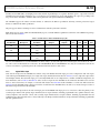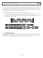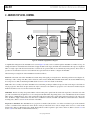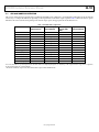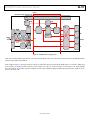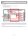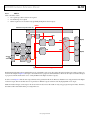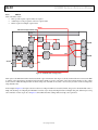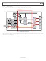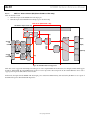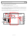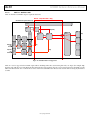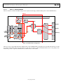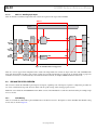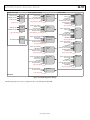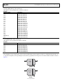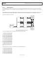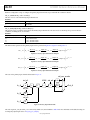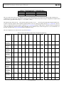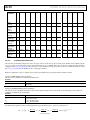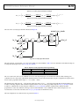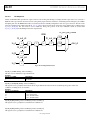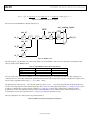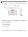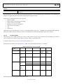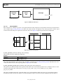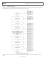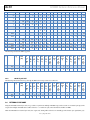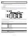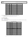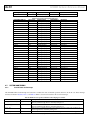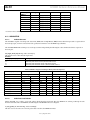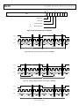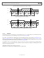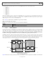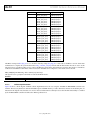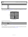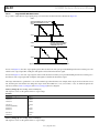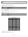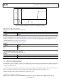
1
ADV8005 Hardware Reference Manual UG-707 One Technology Way • P.O. Box 9106 • Norwood, MA 02062-9106, U.S.A. • Tel: 781.329.4700 • Fax: 781.461.3113 • www.analog.com ADV8005 Functionality and Features PLEASE SEE THE LAST PAGE FOR AN IMPORTANT WARNING AND LEGAL TERMS AND CONDITIONS. Rev. 0 | Page 1 of 326 UG-707 ADV8005 Hardware Reference Manual TABLE OF CONTENTS Understanding the ADV8005 Hardware Manual ............................................................................................................ 9 Description of the Hardware Manual ..........................................................................................................................................9 Disclaimer .......................................................................................................................................................................................9 Trademark and Service Mark Notice ...........................................................................................................................................9 Number Notations..........................................................................................................................................................................9 Register Access Conventions ........................................................................................................................................................9 Acronyms and Abbreviations .......................................................................................................................................................9 Field Function Description ...........................................................................................................................................................12 References........................................................................................................................................................................................13 1. Introduction to the ADV8005 ................................................................................................................................ 14 1.1. Overview..........................................................................................................................................................................14 1.1.1. Digital Video Input ............................................................................................................................................................. 15 1.1.2. Flexible Digital Core ........................................................................................................................................................... 16 1.1.3. Video Signal Processor ....................................................................................................................................................... 16 1.1.4. Bitmap On Screen Display................................................................................................................................................. 17 1.1.5. External DDR2 Memory .................................................................................................................................................... 18 1.1.6. HDMI Transmitter ............................................................................................................................................................. 18 1.1.7. Video Encoder ..................................................................................................................................................................... 18 1.1.8. Digital Video Output .......................................................................................................................................................... 18 1.2. Main Features of the ADV8005 ....................................................................................................................................19 1.2.1. Video Signal Processor ....................................................................................................................................................... 19 1.2.1.1. Primary VSP .......................................................................................................................................................................................... 19 1.2.1.2. Horizontal Pre-Scaler ........................................................................................................................................................................... 19 1.2.1.3. Secondary VSP ...................................................................................................................................................................................... 19 1.2.2. 1.2.3. 1.2.4. 1.2.5. OSD....................................................................................................................................................................................... 19 Video Encoder ..................................................................................................................................................................... 20 HDMI 1.4 Transmitter ....................................................................................................................................................... 20 Additional Features............................................................................................................................................................. 20 1.3. Protocol for Main I2C Port ............................................................................................................................................22 1.4. Configuring the ADV8005 ............................................................................................................................................23 2. ADV8005 Top Level Control .................................................................................................................................. 24 2.1. ADV8005 Modes of Operation.....................................................................................................................................25 2.1.1. Selecting a Mode ................................................................................................................................................................. 26 2.1.2. Mode 1 .................................................................................................................................................................................. 26 2.1.3. Mode 2 .................................................................................................................................................................................. 28 2.1.4. Mode 3 .................................................................................................................................................................................. 29 2.1.5. Mode 4 .................................................................................................................................................................................. 30 2.1.6. Mode 5 .................................................................................................................................................................................. 31 2.1.7. Mode 6 .................................................................................................................................................................................. 32 2.1.8. Mode 7 .................................................................................................................................................................................. 33 2.1.9. Mode 8 .................................................................................................................................................................................. 34 2.1.10. Mode 9 - Bypass .................................................................................................................................................................. 35 2.1.11. Mode 10 – Picture in Picture (PiP) (External OSD Less Than 720p) ......................................................................... 36 2.1.12. Mode 11 – PIP (External OSD Greater Than or Equal To 720p) ................................................................................. 37 2.1.13. Mode 12 – Dual Zone OSD ............................................................................................................................................... 38 Rev. 0 | Page 2 of 326 ADV8005 Hardware Reference Manual 2.1.14. 2.1.15. UG-707 Mode 13 – OSD from HDMI RX ..................................................................................................................................... 39 Mode 14 – Handling Triple Inputs ................................................................................................................................... 40 2.2. ADV8005 Top Level Overview .....................................................................................................................................40 2.2.1. Video Muxing ...................................................................................................................................................................... 40 2.2.2. Digital Video Input ............................................................................................................................................................. 44 2.2.2.1. Video TTL Input ................................................................................................................................................................................... 44 2.2.2.2. EXOSD TTL Input ................................................................................................................................................................................ 45 2.2.2.3. TTL Output ........................................................................................................................................................................................... 45 2.2.2.4. Treatment o f Unused TTL Inputs ..................................................................................................................................................... 47 2.2.2.5. Serial Video Rx ...................................................................................................................................................................................... 51 2.2.2.6. Primary Input Channel ........................................................................................................................................................................ 51 2.2.2.7. Secondary Input Channel .................................................................................................................................................................... 56 2.2.2.8. RX Input Channel ................................................................................................................................................................................. 60 2.2.3. 2.2.4. 2.2.4.1. PVSP Output Timing ........................................................................................................................................................................... 65 2.2.4.2. SVSP Output Timing............................................................................................................................................................................ 66 2.2.4.3. Frame Tracking ..................................................................................................................................................................................... 66 2.2.5. DDR2 Interface ................................................................................................................................................................... 68 2.2.5.1. DDR2 Configuration ............................................................................................................................................................................ 68 2.2.5.2. DDR2 Bandwidth and Memory Selection ........................................................................................................................................ 69 2.2.5.3. Single DDR2 Memory Configuration................................................................................................................................................ 71 2.2.5.4. DDR2 Loopback Test ........................................................................................................................................................................... 72 2.2.6. 2.2.7. 2.2.8. I2C Auto Increment............................................................................................................................................................. 73 SPI Loop Through .............................................................................................................................................................. 73 VBI Data Insertion ............................................................................................................................................................. 74 2.2.8.1. Extraction Overview ............................................................................................................................................................................ 74 2.2.8.2. Ancillary Data Extraction .................................................................................................................................................................... 74 2.2.8.3. SPI Data Extraction .............................................................................................................................................................................. 75 2.2.8.4. VBI Data Delay ..................................................................................................................................................................................... 75 2.2.9. 2.2.10. 2.2.11. 2.2.12. Resets .................................................................................................................................................................................... 76 Image Processing Colorimetry Breakdown .................................................................................................................... 78 AV-Codes ............................................................................................................................................................................. 79 Color Space Conversion ..................................................................................................................................................... 83 2.2.12.1. Primary Input Channel CSC......................................................................................................................................................... 83 2.2.12.2. Secondary Input Channel CSC ..................................................................................................................................................... 86 2.2.12.3. RX Input Channel CSC.................................................................................................................................................................. 89 2.2.12.4. TTL Output CSC ............................................................................................................................................................................ 92 2.2.12.5. HDMI Transmitter CSCs............................................................................................................................................................... 95 2.2.13. 2.2.14. 2.2.15. 3. Updither Configuration ..................................................................................................................................................... 60 Clock Configuration ........................................................................................................................................................... 61 VGA Position and Phase Information ............................................................................................................................. 98 ADV8005 Silicon Revision ................................................................................................................................................ 103 System Configuration......................................................................................................................................................... 103 Video Signal Processing .......................................................................................................................................... 105 3.1. Introduction ....................................................................................................................................................................105 3.2. Primary VSP ....................................................................................................................................................................105 3.2.1. Introduction to PVSP ......................................................................................................................................................... 105 3.2.1.1. Autoconfiguration ................................................................................................................................................................................ 106 3.2.1.2. Customized Input/Output Video Format Configuration ............................................................................................................... 108 3.2.1.3. Field/Frame Buffer Number................................................................................................................................................................ 109 Rev. 0 | Page 3 of 326 UG-707 ADV8005 Hardware Reference Manual 3.2.1.4. Field/Frame Buffer Address and Size................................................................................................................................................. 109 3.2.1.5. Frame Latency ....................................................................................................................................................................................... 111 3.2.1.6. Game Mode ........................................................................................................................................................................................... 112 3.2.1.7. Low Latency Mode ............................................................................................................................................................................... 113 3.2.1.8. Freezing Output Video ......................................................................................................................................................................... 114 3.2.1.9. Progressive Cadence Detection .......................................................................................................................................................... 114 3.2.2. PVSP Video Input Module ................................................................................................................................................ 116 3.2.2.1. VIM Cropper ......................................................................................................................................................................................... 116 3.2.2.2. Horizontal Down Scaler ...................................................................................................................................................................... 118 3.2.2.3. Scaler Interpolation Mode ................................................................................................................................................................... 118 3.2.2.4. Scaler Controls ...................................................................................................................................................................................... 119 3.2.2.5. Pixel Packer ............................................................................................................................................................................................ 119 3.2.3. PVSP Video Output Module ............................................................................................................................................. 120 3.2.3.1. Pixel Unpacker ...................................................................................................................................................................................... 121 3.2.3.2. VOM Cropper ....................................................................................................................................................................................... 121 3.2.3.3. Motion Detection .................................................................................................................................................................................. 122 3.2.3.4. Low Angle De-interlacing ................................................................................................................................................................... 123 3.2.3.5. Cadence Detection................................................................................................................................................................................ 123 3.2.3.6. CUE Correction .................................................................................................................................................................................... 125 3.2.3.7. Random Noise Reduction ................................................................................................................................................................... 125 3.2.3.8. Mosquito Noise Reduction .................................................................................................................................................................. 126 3.2.3.9. Block Noise Reduction ......................................................................................................................................................................... 126 3.2.3.10. Sharpness Enhancement ................................................................................................................................................................ 128 3.2.3.11. Scaler ................................................................................................................................................................................................ 128 3.2.3.12. Panorama Mode .............................................................................................................................................................................. 130 3.2.3.13. Output Port...................................................................................................................................................................................... 131 3.2.3.14. Demo Function ............................................................................................................................................................................... 134 3.2.3.15. Progressive to Interlaced Converter............................................................................................................................................. 135 3.2.3.16. Automatic Contrast Enhancement .............................................................................................................................................. 136 3.3. Secondary VSP ................................................................................................................................................................136 3.3.1. Introduction to SVSP ......................................................................................................................................................... 136 3.3.1.1. Autoconfiguration ................................................................................................................................................................................ 138 3.3.1.2. Customized Input/Output Video Format Configuration ............................................................................................................... 140 3.3.1.3. Frame Buffer Number .......................................................................................................................................................................... 141 3.3.1.4. Frame Buffer Address and Size ........................................................................................................................................................... 141 3.3.1.5. Frame Latency ....................................................................................................................................................................................... 142 3.3.1.6. Freezing Output Video ......................................................................................................................................................................... 144 3.3.2. VIM Cropper ......................................................................................................................................................................................... 144 3.3.2.2. Scaler....................................................................................................................................................................................................... 146 3.3.2.3. Scaler Interpolation Mode ................................................................................................................................................................... 146 3.3.2.4. VIM Miscellaneous Control ................................................................................................................................................................ 147 3.3.2.5. Panorama Mode .................................................................................................................................................................................... 147 3.3.2.6. Pixel Packer ............................................................................................................................................................................................ 148 3.3.3. 3.4. SVSP Video Input Module (VIM) .................................................................................................................................... 144 3.3.2.1. SVSP Video Output Module.............................................................................................................................................. 149 3.3.3.1. Pixel Unpacker ...................................................................................................................................................................................... 149 3.3.3.2. VOM Cropper ....................................................................................................................................................................................... 150 3.3.3.3. Output Port ............................................................................................................................................................................................ 151 3.3.3.4. DDR Bypass Mode ................................................................................................................................................................................ 154 3.3.3.5. Progressive to Interlaced Converter in SVSP.................................................................................................................................... 154 VSP Register Access Protocols ......................................................................................................................................155 Rev. 0 | Page 4 of 326 ADV8005 Hardware Reference Manual 3.4.1. 3.4.2. 3.4.3. 3.4.4. 3.4.5. UG-707 Bootup Protocol .................................................................................................................................................................. 155 Reboot Protocol .................................................................................................................................................................. 156 Gentle Reboot Protocol ...................................................................................................................................................... 158 VOM Set Protocol ............................................................................................................................................................... 159 Free Access Protocol ........................................................................................................................................................... 159 3.5. Horizontal Pre-scaler .....................................................................................................................................................160 3.5.1. HPS Downscaling ............................................................................................................................................................... 162 3.5.2. HPS Upscaling..................................................................................................................................................................... 163 3.5.3. Using the HPS for converting between 3D to 2D Video formats................................................................................. 163 3.5.4. 3D Side by Side Full ............................................................................................................................................................ 165 3.5.5. 3D Side by Side Full ............................................................................................................................................................ 166 3.6. External Sync Mode .......................................................................................................................................................166 3.6.1. Functional Description ...................................................................................................................................................... 167 3.7. Progressive to Interlaced Conversion ..........................................................................................................................169 4. On Screen Display ................................................................................................................................................... 170 4.1. Introduction ....................................................................................................................................................................170 4.1.1. Features ................................................................................................................................................................................ 170 4.1.2. OSD System Application Diagram ................................................................................................................................... 170 4.1.3. Typical OSD Component Sizes ......................................................................................................................................... 171 4.2. Architecture Overview...................................................................................................................................................171 4.2.1. Introduction ........................................................................................................................................................................ 171 4.2.2. Top Level Diagram ............................................................................................................................................................. 171 4.2.3. OSD Blending ...................................................................................................................................................................... 172 4.2.4. External Alpha Blending .................................................................................................................................................... 173 4.2.5. OSD Core ............................................................................................................................................................................. 173 4.2.5.1. OSD Core Region Definition .............................................................................................................................................................. 173 4.2.5.2. OSD Color Space .................................................................................................................................................................................. 175 4.2.6. 4.2.7. 4.2.8. 4.2.8.1. Overview ................................................................................................................................................................................................ 179 4.2.8.2. SPI Slave Interface................................................................................................................................................................................. 183 4.2.8.3. SPI Master Interface ............................................................................................................................................................................. 185 4.2.9. 5. OSD Timers ......................................................................................................................................................................... 175 OSD Scaler ........................................................................................................................................................................... 178 OSD Master/Slave SPI Interface ....................................................................................................................................... 178 OSD Initialization ............................................................................................................................................................... 186 Serial Video Receiver .............................................................................................................................................. 187 5.1. + 5 V Detect ....................................................................................................................................................................187 5.2. TMDS Clock Activity Detection ..................................................................................................................................188 5.3. Clock and Data Termination Control ..........................................................................................................................188 5.4. AV Mute Status ...............................................................................................................................................................189 5.5. Deep Color Mode Support ............................................................................................................................................189 5.6. Video FIFO ......................................................................................................................................................................190 5.7. Pixel Repetition ...............................................................................................................................................................191 5.8. Sync Signal Polarity Readbacks ....................................................................................................................................192 5.9. InfoFrame Registers .......................................................................................................................................................193 5.9.1. InfoFrame Collection Mode .............................................................................................................................................. 193 5.9.2. InfoFrame Checksum Error Flags .................................................................................................................................... 193 5.9.3. AVI InfoFrame Registers ................................................................................................................................................... 195 Rev. 0 | Page 5 of 326 UG-707 5.9.4. 5.9.5. 5.9.6. ADV8005 Hardware Reference Manual SPD InfoFrame Registers ................................................................................................................................................... 196 MPEG Source InfoFrame Registers.................................................................................................................................. 197 Vendor Specific InfoFrame Registers ............................................................................................................................... 197 5.10. Packet Registers ..............................................................................................................................................................198 5.10.1. ISRC Packet Registers......................................................................................................................................................... 198 5.10.2. Gamut Metadata Packets ................................................................................................................................................... 200 5.11. Customizing Packet/InfoFrame Storage Registers .....................................................................................................201 5.12. HDMI Section Reset Strategy .......................................................................................................................................202 6. HDMI Transmitter .................................................................................................................................................. 203 6.1. General Controls ............................................................................................................................................................203 6.2. Reset Strategy ..................................................................................................................................................................205 6.3. HDMI DVI Selection .....................................................................................................................................................205 6.4. AV Mute ...........................................................................................................................................................................205 6.5. Source Product Description InfoFrame ......................................................................................................................206 6.6. Spare Packets and VSI Support .....................................................................................................................................207 6.7. System Monitoring .........................................................................................................................................................210 6.7.1. General Status and Interrupts ........................................................................................................................................... 210 6.8. EDID/HDCP Controller Status ....................................................................................................................................211 6.9. EDID/HDCP Controller Error Codes .........................................................................................................................211 6.10. Video Setup .....................................................................................................................................................................212 6.10.1. Input Format........................................................................................................................................................................ 212 6.10.2. Video Mode Detection ....................................................................................................................................................... 212 6.10.3. Pixel Repetition ................................................................................................................................................................... 213 6.10.4. Video Related Packets and InfoFrames............................................................................................................................ 214 6.10.5. AVI InfoFrame .................................................................................................................................................................... 214 6.10.6. MPEG InfoFrame................................................................................................................................................................ 215 6.10.7. Gamut Metadata ................................................................................................................................................................. 216 6.11. Audio Setup .....................................................................................................................................................................218 6.11.1. Audio Architecture ............................................................................................................................................................. 218 6.11.2. Audio from Serial Video Rx .............................................................................................................................................. 218 6.11.3. Audio Configuration .......................................................................................................................................................... 219 6.11.3.1. I2S Audio ......................................................................................................................................................................................... 221 6.11.3.2. SPDIF Audio ................................................................................................................................................................................... 227 6.11.3.3. DSD Audio ...................................................................................................................................................................................... 228 6.11.3.4. HBR Audio ...................................................................................................................................................................................... 228 6.11.4. N and CTS Parameters ....................................................................................................................................................... 229 6.11.4.1. N Parameter..................................................................................................................................................................................... 230 6.11.4.2. CTS Parameter ................................................................................................................................................................................ 230 6.11.4.3. Recommended N and Expected CTS Values.............................................................................................................................. 230 6.11.5. 6.11.6. 6.11.7. 6.11.8. Audio Sample Packets ........................................................................................................................................................ 232 Audio InfoFrame................................................................................................................................................................. 236 ACP Packet .......................................................................................................................................................................... 237 ISRC Packet ......................................................................................................................................................................... 238 6.12. EDID Handling ...............................................................................................................................................................240 6.12.1. Reading the EDID............................................................................................................................................................... 240 6.12.2. EDID Definitions ................................................................................................................................................................ 240 6.12.3. Additional Segments .......................................................................................................................................................... 240 Rev. 0 | Page 6 of 326 ADV8005 Hardware Reference Manual 6.12.4. 6.12.5. UG-707 edid_tries Control ............................................................................................................................................................... 241 EDID Reread Control......................................................................................................................................................... 241 6.13. HDCP Handling .............................................................................................................................................................242 6.13.1. One Sink and No Upstream Devices ................................................................................................................................ 242 6.13.2. Multiple Sinks and No Upstream Devices ....................................................................................................................... 243 6.13.3. Software Implementation .................................................................................................................................................. 244 6.13.4. AV Mute ............................................................................................................................................................................... 246 6.14. Audio Return Channel ...................................................................................................................................................246 6.15. Charge Injection Settings ..............................................................................................................................................247 6.16. Enabling and Disabling the HDMI TMDS Otuputs ..................................................................................................247 6.17. HDMI TX Source Termination ....................................................................................................................................248 6.18. HDMI ACR Packet Transmission ................................................................................................................................249 7. Video Encoder Introduction to the ADV8005 ....................................................................................................... 250 7.1. Introduction ....................................................................................................................................................................250 7.2. Input Configuration .......................................................................................................................................................250 7.3. Output Configuration ....................................................................................................................................................253 7.4. Additional Design Features ...........................................................................................................................................254 7.4.1. Output Oversampling ........................................................................................................................................................ 254 7.4.2. Subcarrier Frequency Lock (SFL) Mode......................................................................................................................... 255 7.4.3. SD VCR FF/RW Synchronization..................................................................................................................................... 256 7.4.4. Vertical Blanking Interval .................................................................................................................................................. 256 7.4.5. SD Subcarrier Frequency Control .................................................................................................................................... 256 7.4.5.1. 7.4.6. 7.4.7. Programming the FSC ......................................................................................................................................................................... 257 SD Non Interlaced Mode (240p/288p) ............................................................................................................................ 257 Filters .................................................................................................................................................................................... 257 7.4.7.1. SD Filters ................................................................................................................................................................................................ 257 7.4.7.2. ED/HD Filters ....................................................................................................................................................................................... 260 7.4.8. 7.4.9. 7.4.10. ED/HD Test Pattern Generator......................................................................................................................................... 261 Color Space Conversion Matrix ........................................................................................................................................ 262 ED/HD Manual CSC Matrix Adjust Feature .................................................................................................................. 262 7.4.10.1. 7.4.11. 7.4.12. 7.4.13. 7.4.14. 7.4.15. Programming the CSC Matrix...................................................................................................................................................... 264 SD Luma and Color Scale Control ................................................................................................................................... 264 SD Hue Adjust Control ...................................................................................................................................................... 265 SD Brightness Detect .......................................................................................................................................................... 266 SD Brightness Control ....................................................................................................................................................... 266 Double Buffering................................................................................................................................................................. 267 7.4.15.1. ED/HD Doubling Buffering.......................................................................................................................................................... 267 7.4.15.2. SD Doubling Buffering .................................................................................................................................................................. 267 7.4.16. 7.4.17. Programmable DAC Gain Control ................................................................................................................................... 268 Gamma Correction............................................................................................................................................................. 269 7.4.17.1. ED/HD Gamma Correction ......................................................................................................................................................... 271 7.4.17.2. SD Gamma Correction .................................................................................................................................................................. 272 7.4.18. ED/HD Sharpness Filter and Adaptive Filter Controls ................................................................................................. 273 7.4.18.1. ED/HD Sharpness Filter Mode..................................................................................................................................................... 273 7.4.18.2. ED/HD Adaptive Filters ................................................................................................................................................................ 274 7.4.18.3. ED/HD Adaptive Filter Modes ..................................................................................................................................................... 276 7.4.18.4. ED/HD Sharpness Filter and Adaptive Filter Application Examples ..................................................................................... 276 7.4.19. SD Digital Noise Reduction .............................................................................................................................................. 278 Rev. 0 | Page 7 of 326 UG-707 7.4.19.1. Coring Gain Border .......................................................................................................................................................................279 7.4.19.2. Coring Gain Data ...........................................................................................................................................................................280 7.4.19.3. DNR Threshold...............................................................................................................................................................................280 7.4.19.4. Border Area .....................................................................................................................................................................................281 7.4.19.5. Block Size Control ..........................................................................................................................................................................281 7.4.19.6. DNR Input Select Control .............................................................................................................................................................281 7.4.19.7. DNR Mode Control........................................................................................................................................................................282 7.4.19.8. DNR Block Offset Control ............................................................................................................................................................282 7.4.19.9. SD Active Video Edge Control .....................................................................................................................................................283 7.5. 7.6. Vertical Blanking Interval..............................................................................................................................................284 DAC Configurations ......................................................................................................................................................285 7.6.1. 7.6.2. 8. ADV8005 Hardware Reference Manual Voltage Reference ................................................................................................................................................................ 285 Video Output Buffer and Optional Output Filter .......................................................................................................... 285 Interrupts................................................................................................................................................................. 288 8.1. Interrupt Pins ..................................................................................................................................................................288 8.1.1. 8.1.2. 8.2. Interrupt Duration .............................................................................................................................................................. 288 Storing Masked Interrupts ................................................................................................................................................. 289 Serial Video Rx Interrupts .............................................................................................................................................289 8.2.1. 8.2.2. Introduction ........................................................................................................................................................................ 289 Interrupt Architecture Overview ...................................................................................................................................... 292 8.2.2.1. 8.2.3. 8.3. 8.3.1. 8.4. 8.4.1. 8.4.2. 8.4.3. Multiple Interrupt Events ....................................................................................................................................................................293 Serial Video Interrupts Validity Checking Process ........................................................................................................ 293 VSP and OSD Section ....................................................................................................................................................293 Interrupt Architecture Overview ...................................................................................................................................... 294 HDMI Tx core.................................................................................................................................................................294 Introduction ........................................................................................................................................................................ 294 Interrupt Architecture Overview ...................................................................................................................................... 294 HDMI Tx Interrupt Polarity ............................................................................................................................................. 295 Appendix A ....................................................................................................................................................................... 296 PCB Layout Recommendations....................................................................................................................................................296 Analogue/Digital Video Interface Outputs ...................................................................................................................................... 296 External DDR2 Memory Requirements ........................................................................................................................................... 296 Power Supply Bypassing ..................................................................................................................................................................... 297 General Digital Inputs and Outputs ................................................................................................................................................. 297 XTAL and Load Cap Value Selection................................................................................................................................................ 297 Encoder Component Placement ....................................................................................................................................................... 298 HDMI Transmitter Component Placement..................................................................................................................................... 298 Power Supply Design and Sequencing.............................................................................................................................................. 298 Appendix B........................................................................................................................................................................ 301 Unused Pin List ..............................................................................................................................................................................301 Appendix C ....................................................................................................................................................................... 313 Pixel Input and Output Formats...................................................................................................................................................313 Revision History 6/14—Revision 0: Initial Version Rev. 0 | Page 8 of 326 ADV8005 Hardware Reference Manual UG-707 UNDERSTANDING THE ADV8005 HARDWARE MANUAL DESCRIPTION OF THE HARDWARE MANUAL This manual provides a detailed description of the functionality and features supported by the ADV8005. DISCLAIMER The information contained in this document is proprietary of Analog Devices Inc. (ADI). This document must not be made available to anybody other than the intended recipient without the written permission of ADI. The content of this document is believed to be correct. If any errors are found within this document or, if clarification is needed, contact the authors at [email protected]. TRADEMARK AND SERVICE MARK NOTICE The Analog Devices logo is a registered trademark of Analog Devices, Inc. All other brand and product names are trademarks or service marks of their respective owners. NUMBER NOTATIONS Notation bit N V[X:Y] 0xNN 0bNN NN Description Bits are numbered in little endian format, that is, the least significant bit of a number is referred to as Bit 0 Bit field representation covering bit X to Y of a value or a field V Hexadecimal (base-16) numbers are preceded by the prefix ‘0x’ Binary (base-2) numbers are preceded by the prefix ‘0b’ Decimal (base-10) are represented using no additional prefixes or suffixes REGISTER ACCESS CONVENTIONS Mode R/W R W Description Memory location has read and write access. Memory location has read access only. A read always returns 0 unless specified otherwise. Memory location has write access only. ACRONYMS AND ABBREVIATIONS This is a list of common acronyms and abbreviations found in Analog Devices Hardware Manuals. Acronym/Abbreviation ACP ACR ADC AFE AGC Ainfo AKSV An ARC AUD_IN AVI Aux Bcaps Description Audio Content Protection Audio Clock Regeneration Analog to Digital Converter Analog Front End Automatic Gain Control HDCP register. Refer to HDCP documentation. HDCP Transmitter Key Selection Vector. Refer to HDCP documentation. 64-bit pseudo-random value generated by HDCP cipher function of device A Audio Return Channel Audio Input Pin Auxiliary Video Information Auxiliary HDCP register. Refer to HDCP documentation. Rev. 0 | Page 9 of 326 UG-707 Acronym/Abbreviation BGA BKSV BNR CEC CP CSC CSync CTS CUE CVBS DCM DDR DDFS DE DID DLL DMA DNR DPP DSD DST DUT DVD DVI EAV ED ENC EQ FFS FRC HBR HD HDCP HDMI HDTV HEAC HEC HPA HPD HSync/HS IC ISRC I2 S I2 C KSV LLC LQFP LSB L-PCM Mbps MNR ADV8005 Hardware Reference Manual Description Ball Grid Array HDCP Receiver Key Selection Vector. Refer to HDCP documentation. Block Noise Reduction Consumer Electronics Control Component Processor Color Space Converter/Conversion Composite Synchronization Cycle Time Stamp Color Upsampling Error Composite Video Decimation Double Data Rate Direct Digital Frequency Synthesizer Data Enable Data Identification Word Delay Locked Loop Direct Memory Access Digital Noise Reduction Data Preprocessor Direct Stream Digital Direct Stream Transfer Device Under Test (designate the ADV8005 unless stated otherwise) Digital Video Disc Digital Visual Interface End of Active Video Enhanced Definition Encoder Equalizer Field Frame Scheduler Frame Rate Conversion/Converter High Bit Rate High Definition High Bandwidth Digital Content Protection High Definition Multimedia Interface High Definition Television HDMI Ethernet and Audio Channels HDMI Ethernet Channel Hot Plug Assert Hot Plug Detect Horizontal Synchronization Integrated Circuit International Standard Recording Code Inter IC Sound Inter Integrated Circuit Key Selection Vector Line Locked Clock Low-profile Quad Flat Package Least Significant Bit Linear Pulse Code Modulation Megabit per Second Mosquito Noise Reduction Rev. 0 | Page 10 of 326 ADV8005 Hardware Reference Manual Acronym/Abbreviation MPEG ms MSB NC NSV OSD OTP PtoI Pj’ PVSP Ri’ RNR Rx SA SAV SD SDP SDR SMPTE SNR SOG SOY SPA SPD SPDIF SPI SRM SSPD STDI SVSP TBC TMDS Tx ULAI US VBI VDP VIC VIM VOM VSDP VSP VSync/VS XTAL UG-707 Description Moving Picture Expert Group Millisecond Most Significant Bit No Connect Noise Shaped Video On Screen Display One Time Programmable Progressive to Interlaced HDCP Enhanced Link Verification Response. Refer to HDCP documentation. Primary VSP HDCP Link verification response. Refer to HDCP documentation. Random Noise Reduction Receiver Slave Address Start of Active Video Standard Definition Standard Definition Processor Single Data Rate Society of Motion Picture and Television Engineers Signal to Noise Ratio Sync on Green Sync on Y Source Physical Address Source Production/Product Descriptor Sony/Philips Digital Interface Serial Peripheral Interface System Renewability Message Synchronization Source Polarity Detector Standard Identification Secondary VSP Timebase Correction Transition Minimized Differential Signaling Transmitter Ultra Low Angle Interpolation Up Sampling Video Blanking Interval VBI Data Processor Video Identification Code Video Input Module Video Output Module Vendor Specific Data Block Video Signal Processor/Processing Vertical Synchronization Crystal Oscillator Rev. 0 | Page 11 of 326 UG-707 ADV8005 Hardware Reference Manual FIELD FUNCTION DESCRIPTION The function of a field is described in a table preceded by the bit name, a short function description, the I2C map, the register location within the I2C map, and a detailed description of the field. Refer to Error! Reference source not found. for more details. The detailed description consists of: • For a readable field, the values the field can take • For a writable field, the values the field can be set to I2C location of the field in big endian format (MSB first, LSB last) The name of the field. In this example the field is called deep_color_mode and is 2 bits long. deep_color_mode[1:0], HDMI RX Map, Address 0xE20B[7:6] (Read Only) A readback of the deep color mode information extracted from the general control packet. Function deep_color_mode[1:0] 00 01 10 11 Values the field can be set to or take. These values are in binary format if not preceded by ‘0x’ and in hexadecimal format if preceded by ‘0x’. Description 8-bits per channel 10-bits per channel 12-bits per channel 16-bits per channel (not supported) Default value indicated by Figure 1. Field Description Format Rev. 0 | Page 12 of 326 Read/Write Access for field Detailed description of the field ADV8005 Hardware Reference Manual UG-707 REFERENCES HDMI Licensing and LLC, High-Definition Multimedia Interface, Revision 1.4a, March 4, 2010 Digital Content Protection (DCP) LLC, High-bandwidth Digital Content Protection System, Revision 1.3, December 21, 2006 CEA, CEA-861-E, A DTV Profile for Uncompressed High Speed Digital Interfaces, Revision E, September 11, 2007 ITU, ITU-R BT.656-4, Interface for Digital Component Video Signals in 525-Line and 625-Line Television Systems Operating at the 4:2:2 Level of Recommendation ITU-R BT.601, February 1998 ITU, ITU-R BT.601-5 Studio encoding parameters of digital television for standard 4:3 and widescreen 16:9 aspect ratios, December 1995 ITU, ITU-R BT.709-5 Parameter values for the HDTV standards for production and international programme exchange, April 2002 CENELEC, EN 50157, Part 1, Domestic and similar electronic equipment interconnection requirements: AV.link CENELEC, EN 50157, Part 2-1, Domestic and similar electronic equipment interconnection requirements: AV.link CENELEC, EN 50157, Part 2-2, Domestic and similar electronic equipment interconnection requirements: AV.link CENELEC, EN 50157, Part 2-3, Domestic and similar electronic equipment interconnection requirements: AV.link Rev. 0 | Page 13 of 326 UG-707 ADV8005 Hardware Reference Manual 1. INTRODUCTION TO THE ADV8005 1.1. OVERVIEW The ADV8005 is a video signal processor (VSP) with TTL and Serial Video inputs that can de-interlace and scale input video, generate and blend a bitmap based on-screen display (OSD) and output the blended video using one or more of the part’s outputs; dual HDMI transmitters and a 6-DAC encoder with SD and HD support. The ADV8005 has three video inputs – the video TTL input, the EXOSD TTL input and the Serial Video receiver (Rx). The combined video TTL input and EXOSD TTL input constitute the flexible 60-bit TTL input port. The 60-bit TTL input port can be arranged in a variety of fashions to accept one input video stream (for example, a 48-bit 3 GHz input video stream from ADV7619) or two input video streams (for example, a 36-bit input video stream from ADV7844 and a 24-bit input video stream from an external OSD generator). Once the data is received, the video TTL and EXOSD TTL inputs can be connected to either the primary input channel or the secondary input channel. From these input channels, the video data can be sent to the internal video processing blocks (for example, primary VSP or secondary VSP). The Serial Video Rx is connected to the RX input channel. The Serial Video Rx accommodates inter-chip transfer of data over an HDMI compatible interface (for example, from an HDMI (Rx) such as ADV7850 or transceiver such as ADV7623). The ADV8005 does not support EDID or DDC activity on this port. The motion adaptive de-interlacer in the ADV8005 provides excellent edge detection and excellent ultra-low angle performance. Per-pixel motion-adaptive de-interlacing is used for natively interlaced input video (for example, a live sport broadcast) where still parts of the image are reconstructed from information on both the odd and even fields, and moving parts of the image are interpolated by an advanced interpolation algorithm. The de-interlacer can also recognize when interlaced input video originally came from progressive content (for example, 24 Hz movie content or 30 Hz documentary content) and reconstructs the original frames. Dual video scalers allow the ADV8005 to support two different output resolutions on its outputs, for example, 1080p60 on HDMI Tx1 and 720p on HDMI Tx2 and the HD encoder. The primary VSP (PVSP) in the ADV8005 is capable of upscaling from 480i to 4k x 2k formats. The secondary VSP (SVSP) in the ADV8005 is used to provide a second output resolution to accommodate dual zone systems. The ADV8005 is also capable of downscaling a single 4Kx2K input to 1080p or lower using a combination of a Horizontal Pre-Scaler (HPS) and the SVSP. Also available in the ADV8005 are image enhancing features such as random noise reduction (RNR), mosquito noise reduction (MNR) and block noise reduction (BNR), detail enhancement and automatic contrast enhancement (ACE). The ADV8005 features an internal bitmap based OSD generator capable of generating OSDs of up to 4k x 2k. External solutions can also be implemented and fed into the ADV8005 for blending with the main video. A bitmap based OSD is an advanced form of OSD display, which can add effects such as scrolling, animation and 3D depth to OSD displays. This allows customers to create advanced OSD designs to differentiate their products. Once created, OSD designs are stored in an external SPI flash memory connected to the ADV8005. The control of the OSD must be performed from the system microcontroller via SPI. OSD designs can be created using ADI’s software development tool, Blimp OSD. The ADV8005 offers flexible configuration of its internal circuitry allowing the output of one, two or three input channels simultaneously. The output of multiple ADV8005s can be synchronized using the master clock, horizontal sync and vertical sync inputs. This facilitates, with the incorporation of a simple FPGA, seamless per pixel switching of multiple synchronized ADV8005 inputs. The ADV8005 can also measure the picture position and sample quality of the video being processed; this assists in identifying the exact video format and the optimum sampling phase of the video front end’s ADC. Video can be output from the ADV8005 via one or both of the HDMI transmitters, the 6-DAC SD/HD video encoder or using the TTL interface. Both HDMI transmitters support the HDMI v1.4b specifications of increased resolutions, 3D video and audio return channel (ARC). The ADV8005 supports both S/PDIF and 8-channel I2S audio. . The audio can be sourced from either the external audio interface or using the audio pass through feature of the Serial Video Rx. The ADV8005 includes a high-speed digital-to-analog video encoder available with and without Rovi content protection. Six high speed, Noise Shaped Video (NSV), 12-bit video DACs provide support for composite (CVBS), S-video (Y/C), and component (YPrPb/RGB) analog outputs in either SD, ED, or HD video formats up to 1080p. In addition, simultaneous SD and ED/HD formats are supported. 216 MHz (SD Rev. 0 | Page 14 of 326 ADV8005 Hardware Reference Manual UG-707 and ED) and 297 MHz (HD) oversampling ensures that external output filtering is not required. The final option to output video from the ADV8005 is the TTL interface which allows up to 36 of the pins to be reconfigured as outputs. This facilitates the output of up to 1080p 12-bit deep color from the ADV8005 to an FPGA without the requirement of an expensive FPGA-based HDMI phy. The ADV8005 supports all common consumer formats as outlined in the EIA-861 specification and many common professional output formats as outlined in the VESA specification. The part supports the I2C® and SPI protocols for communication with the system microcontroller. Note: There are four options within the ADV8005 family of parts, each with different capabilities but all in the same CSPBGA-425 package. These are described in Table 1. Part Number ADV8005KBCZ8A ADV8005KBCZ8N ADV8005KBCZ-8B Max Speed 3 Gbps ADV8005KBCZ-8C 3 Gbps 3 Gbps 3 Gbps Table 1: Available Features Within ADV8005 Family of ICs HDMI Tx Maximum Analog Resolution Outputs Outputs 4k × 2k at 30 Hz (82 Six 12-bit DACs bit) 4k × 2k at 30 Hz (82 Six 12-bit DACs bit) 4k × 2k at 30 Hz (81 No bit) 4k × 2k at 30 Hz (82 No bit) Rovi Yes VSP 2 OSD Yes TTL Out Yes No 2 Yes Yes N/A 1 Yes No N/A 2 Yes No Note that ADV8005KBCZ-8A and ADV8005KBCZ-8N functionality is described throughout this manual (figures, functional blocks, and so on). Some sections of this manual are not relevant to the ADV8005KBCZ-8B and ADV8005KBCZ-8C as they do not include those blocks. If a section is not relevant to a particular generic, this is indicated in the introduction to that section. 1.1.1. Digital Video Input Video data can be input into the ADV8005 in a number of ways. The flexible 60-bit TTL input port can be configured for dual video inputs (video TTL input and EXOSD TTL input), for a single video input (interleaved TTL data from an ADV7619) or for a single video input and an external alpha channel. The 60-bit TTL input port is extremely flexible and can be configured into a number of different arrangements; for more information, refer to Table 87 and Table 88. Video can also be input into the ADV8005 via the Serial Video Rx which can be used for device to device interconnect, for example, a serial video link between the ADV7850 and the ADV8005 or a serial video link between the ADV7623 and the ADV8005. Using such front end devices located before the ADV8005 allows the audio to be extracted and processed in a DSP before being reinserted into the ADV8005. A mux after the TTL inputs allows the video TTL input pins and the EXOSD TTL input pins to be connected to either the primary or the secondary input channel. The primary input channel features an input formatter, manually programmable CSC, updither function, ACE, contrast, brightness and saturation controls. The secondary input channel features an input formatter, manually programmable CSC and updither function. The Serial Video Rx is connected directly to the Rx input channel and features an input formatter, manually programmable CSC and updither function. Rev. 0 | Page 15 of 326 UG-707 ADV8005 Hardware Reference Manual ADV8005 EXOSD OS2D4-b 2i4t -bit In Inppuut t 60-bi t TTL Input Vid eo Vid eo 36/48 36-bi t -bit Input Input Secondary Input Channel IN P U T F MT D IT HER +C S C H igh Sp eed eed O Primary Input Channel 148.5MHz to 300MHz Conversion E D IT H E R +C SC + ACE IN P U T F MT H igh Spee d I Rx Serial Video RX eo RX Input Channel IN P U T F MT D IT H E R +CS C Figure 2: ADV8005 Digital Video Interface 1.1.2. Flexible Digital Core The ADV8005 has a flexible digital core, allowing multiple options for the routing of video data. This allows the user to place the OSD in front of the video processing so the OSD will be overlaid on one or more outputs. Alternatively, video processing can be placed before the OSD ensuring all outputs are processed to the highest quality. The digital core can also be configured so that the ADV8005 can output one or all of the inputs in various arrangements, for example, picture in picture with one input appearing as a window within another or two inputs routed to two outputs. Several common modes of operation are defined to assist the user to quickly integrate the ADV8005 into a system. Refer to Section 2 for more details. 1.1.3. Video Signal Processor The motion adaptive de-interlacer in the ADV8005 offers excellent edge detection and ultra low angle performance. The per-pixel deinterlacing algorithm used delivers excellent performance which can be seen with specialist test patterns, on facial features like eyebrows or on shirt collars. This algorithm decides on whether an area of an image is moving or not and then applies the appropriate de-interlacing approach accordingly. The de-interlacer can also determine when interlaced video originated as progressive and can reconstruct the original frames. Low Angle Processing Cadence Detection Motion Detection CUE Correction De-interlacer Detail Enhance Colour Enhance Dual and l Scaler DuaScaler OSD Blend and FRC Noise Reduction Enhance Figure 3: ADV8005 Video Processing The ADV80038005 features dual scalers referred to as Primary Video Signal Processor (PVSP) and the Secondary Video Signal Processor (SVSP). The PVSP uses a contour-based interpolation scaler which can upscale from 480i to 4k x 2k. The PVSP can arbitrarily upscale between 480p and 4k x 2k and down scale between 1080p and 480p. The advanced scaling algorithm used in the ADV8005 eradicates many common problems associated with scaling video such as ringing and jagged or blurred edges. Using a combination of the Horizontal Pre Scaler (HPS) Rev. 0 | Page 16 of 326 ADV8005 Hardware Reference Manual UG-707 and the SVSP, the ADV8005 can downscale from 4k x 2k to 1080p. The PVSP can be employed to further scale the downscaled 4k x 2k content. When using the PVSP as the primary scaler, the SVSP can also be used to provide a second lower resolution output format. The PVSP and SVSP can be connected in parallel or in series. The ADV8005 features a number of video enhancement controls such as detail enhancement, block noise reduction, mosquito noise reduction and random noise reduction. Block and mosquito noise are related to the compression of video for transmission or encoding onto a DVD or BD disc. Random noise is related to noise picked up during the transmission of video. The automatic contrast enhancement feature offered by the ADV8005 intelligently stretches the brightness of an image to enhance the dark areas without saturating the dark areas. Note that the dual scaler variants of the ADV8005 are the following: • ADV8005KBCZ-8A/8N • ADV8005KBCZ-8C The single scaler variants of the ADV8005 are the following: • ADV8005KBCZ-8B 1.1.4. Bitmap On Screen Display The ADV8005 incorporates an OSD core capable of generating an internal bitmap based OSD. Customers can generate elaborate OSD designs that can include bitmap images, 3D overlay and animation. Up to 256 regions in total can be created and displayed. These 256 regions are bitmap images defined during the design stage and can be characters, pictures, buttons, and so on. Individual regions can be alpha blended and prioritized versus other regions. SPI DDR2 Internal OSD Generator OSD Build OSD Scaler External OSD Video 1 OSD Blend Video 2 Figure 4: ADV8005 Bitmap OSD The OSD is controlled by the host microcontroller via the ADV8005 SPI slave (serial port 1). In response to commands, the ADV8005 loads the data from the external SPI flash memory via the SPI master (serial port 2). The ADV8005 uses DDR2 memory when rendering and blending the OSD. In order to lower the load of the DDR2 memory, there is a block in the ADV8005 OSD hardware called the OSD coprocessor. The OSD co-processor is responsible for handling upper level commands from the microcontroller and translating them into lower level operations for the OSD and DMA which retrieves data from the external DDR2 memories. The OSD blend can be switched between either of the two video streams routed through the OSD blend block without disturbing the output video. This enables seamless OSD blending in dual zone systems. Bitmap OSDs can be created and compiled using ADI’s software development tool, Blimp OSD. This allows users to create their custom OSDs and emulate them before integrating them into their system, abstracting the design task from the underlying OSD hardware. For more details on the operation of the external OSD, design and system techniques, refer to the Blimp OSD documentation. Rev. 0 | Page 17 of 326 UG-707 1.1.5. ADV8005 Hardware Reference Manual External DDR2 Memory DDR2 Interface Motion Adaptive De-interlacer Frame Rate Conversion Bitmap OSD Data Figure 5: External DDR2 Memory Interface External DDR2 memory is required for motion adaptive de-interlacing, Frame Rate Conversion (FRC), and OSD bitmap overlay. ADV8005 supports various memory options using one or two DDR2 memories of various sizes (1 Gb maximum). For full processing capabilities, two DDR2 memories are required which use data transfers up to 250 MHz. Refer to Section 3 for more details on the operations using the external DDR2 memory. 1.1.6. HDMI Transmitter The ADV8005 features two HDMI v1.4b transmitters. The transmitters feature an audio return channel (ARC), which allows a Sony/Philips Digital Interface (SPDIF) audio connection between the source and sink. Each transmitter features an on-chip MPU with an I2C master to perform HDCP operations and EDID operations. Note: The dual transmitter variants of the ADV8005 are ADV8005KBCZ-8A, ADV8005KBCZ-8N and ADV8005KBCZ-8C. The single transmitter variant of the ADV8005 is the ADV8005KBCZ-8B. 1.1.7. Video Encoder The ADV8005 features a high speed digital to analog video encoder. Six high speed, NSV, 3.3 V, 12-bit video DACs provide support for worldwide composite (CVBS), S-Video (Y-C), and component (YPrPb/RGB) analog outputs in standard definition (SD), enhanced definition (ED), or high definition (HD) video formats. It is also possible to enable the ADV8005 video encoder to work in simultaneous mode where both an SD and ED/HD format are being output. Note: The video encoder variants of the ADV8005 are the ADV8005KBCZ-8A and the ADV8005KBCZ-8N. The variants of ADV8005 with no encoder are the ADV8005KBCZ-8B and the ADV8005KBCZ-8B. 1.1.8. Digital Video Output Video can be output from the ADV8005 via the flexible TTL port. Reusing up to 36 of the flexible TTL port pins means that video can be routed in and out of the ADV8005 without using HDMI, a useful cost reduction in systems which utilize FPGA interconnects (e.g. 30-bit TTL input and 30-bit TTL output allowing 1080p 10-bit input and output). The possible configurations of the TTL output port are captured in Table 90 and Table 91. The video TTL output port has a manually programmable CSC. Rev. 0 | Page 18 of 326 ADV8005 Hardware Reference Manual UG-707 1.2. MAIN FEATURES OF THE ADV8005 1.2.1. Video Signal Processor 1.2.1.1. Primary VSP • • • • • • • • • • • • • • • • • • • • 1.2.1.2. 12-bit internal processing Fixed frame latency capability Input timing up to 1080p Output timing up to 4k x 2k Input/output format YCbCr at 4:4:4 Motion adaptive de-interlacing with motion detection Ultra low angle interpolation on edge regions of interlaced video Cadence detection (any cadence detection possible) Progressive cadence supported Super resolution video scaler Aspect ratio conversion/panorama scaling Arbitrary upscaling and downscaling for both horizontal and vertical direction Sharpness detail and edge enhancement Noise reduction for random, mosquito, and block noise Frame Rate Conversion Color Upsampling Error (CUE) correction Progressive to interlaced (PtoI) converter Game mode supported Album mode supported Demo window Horizontal Pre-Scaler • 8-bit internal processing • Downscales video standards of greater than 162MHz and/or more than 2048 pixels/line 1.2.1.3. • • • • • • • 1.2.2. • • • • • • • • Secondary VSP 8-bit internal processing Input and output timing up to 1080p Input and output format YCbCr at 4:4:4 Up-scaling and down-scaling for both horizontal and vertical direction Aspect ratio conversion and panorama scaling Frame Rate Conversion Progressive to interlaced (PtoI) converter OSD Internally generated bitmap based OSD allowing overlay of bitmap images on one or more video outputs Dual video paths through the OSD blend block to support dual zone OSD Dedicated OSD scaler – allows OSDs to be rendered at a single resolution reducing external memory bandwidth Blending onto 3 GHz video formats Pixel-by-pixel alpha blending of OSD data on video data Option of externally generated OSD OSD can be overlaid in the main 3D video format timings Blimp OSD software tool and provided ANSI-C libraries cover the full design flow of any OSD Rev. 0 | Page 19 of 326 UG-707 1.2.3. • • • • • 1.2.4. ADV8005 Hardware Reference Manual Video Encoder Six NSV 12-bit video DACs Compliant with all common SMPTE formats Multiformat video output support o NTSC M, PAL B/D/G/H/I/M/N, PAL 60 support o Composite (CVBS) and S-Video (Y/C) component/YPrPb/RGB (SD, ED and HD) Macrovision® Rev 7.1.L1 (SD) and Rev 1.2 (ED) compliant Simultaneous SD and ED/HD operation HDMI 1.4 Transmitter • • 3 GHz video output (ADV8005KBCZ-8A/8N models only) Incorporates HDMI™ (v.1.4 with Deep Color, x.v.Color™) o Content Type Bits o ARC (Audio Return Channel) Support o 3D support • • • Supports standard S/PDIF for stereo LPCM compressed audio up to 192 kHz Six-channel uncompressed LPCM I2S audio up to 192 kHz Six-channel DSD audio inputs 1.2.5. • • Additional Features Auto-phase and position detection External Sync Timing mode employing Master clock, horizontal sync and vertical sync inputs Rev. 0 | Page 20 of 326 ADV8005 Hardware Reference Manual UG-707 OSD_IN[23:16]/ EXT_DIN[7:0], OSD_IN[11:0] OSD_IN[15:13]/ VBI_x XTALN XTALP INT0 INT1 INT2 SPI SLAVE CLOCK GENERATION TO VBI INSERTION IN ENCODER BLOCK MOSQUITO NOISE REDUCTION SCALER 2 CADENCE DETECTION BLOCK NOISE REDUCTION FRAME RATE CONVERTER CUE CORRECTION DETAIL ENHANCEMENT HDMI Tx VIDEO DATA CAPTURE OSD SCALER VIDEO PROCESSING AND OSD BLENDING HEAC TOP LEVEL CONTROL MASTER TIMING BLOCK POWER SUPPLY RESET GENERATION AND POWER MANAGEMENT BITMAP OSD CONTROLLER SCALER 1 LOW ANGLE PROCESSING HDCP ENCRYPTION I/O, OSD, ENCODER VSP, HDMI Tx REGISTER MAPS CONTROL ARC PORT SPI SLAVE SPI MASTER I2C SLAVE TX2_0+ TX2_0– TX2_1+ TX2_1– TX2_2+ TX2_2– TX2_C+ TX2_C– ENCODER PROGRAMMABLE HDTV FILTERS PROGRAMMABLE LUMINANCE FILTERS SYNC INSERTION PROGRAMMABLE CHROMINANCE FILTERS SIN/COS MODULATION/COS SHARPNESS AND ADAPTIVE FILTER CONTROL VBI DATA SERVICE INSERTION TX1_0+ TX1_0– TX1_1+ TX1_1– TX1_2+ TX1_2– TX1_C+ TX1_C– HDCP KEYS TMDS OUTPUTS SUBCARRIER FREQ LOCK 12-BIT DAC1 DAC1 12-BIT DAC2 DAC2 12-BIT DAC3 DAC3 12-BIT DAC4 DAC4 12-BIT DAC5 DAC5 12-BIT DAC6 DAC6 REFERENCE AND CABLE DETECTION COMPx RSETx VREF ELPFx SFL ALSB Rev. 0 | Page 21 of 326 SCL SDA CS2 SCK2 MISO2 MOSI2 CS1 SCK1 MISO1 MOSI1 HEAC_1– HEAC_1+ HEAC_2– HEAC_2+ ARC1_OUT ARC2_OUT REF_CLK REF_HS REF_VS DVDD_IO PVDD_DDR AVDDx DVDD_DDR CVDD1 PVDDx DVDD PDN RESET Figure 6. ADV8005 Functional Block Diagram 4:2:2 4:4:4 AND COLOR SPACE CONVERTER MULTIPLEXER OSD VIDEO CAPTURE AND FORMATTING COLOR SPACE CONVERSION OSD_DE OSD_CLK OSD_IN[12] MOTION DETECTION OSD GENERATION 16×/4× OVERSAMPLING FILTERS OSD_VS RANDOM NOISE REDUCTION TMDS OUTPUTS 12074-003 MUXING COLOR SPACE CONVERSION UPDITHER OSD_HS SCALING AND FRAME RATE CONVERSION 4:4:4 AND COLOR SPACE CONVERTER HDCP KEYS 4:2:2 2 × PLLs PCLK VIDEO ENHANCEMENT DE-INTERLACER AND CADENCE DETECTION HPD_TX1 HPD_TX2 ED/HD PROCESSOR DE DIGITAL VIDEO CAPTURE AND FORMATTING DDC1_SC L DDC1_SD A DDC2_SC L DDC2_SD A I 2C MASTER HDCP ENCRYPTION SD PROCESSOR VS HDMI Tx VIDEO DATA CAPTURE VIDEO MUXING HS OSD VIDEO BLEND COLOR SPACE CONVERSION UPDITHER P[35:0] HDCP AND EDID MICROCONTROLLER AUTOPOSITION AUTO-PHASE COLOR SPACE CONVERSION UPDITHER RECEIVER DSD_CLK DDR2 INTERFACE RX_0 P RX_0N RX_1 P RX_1N RX_2 P RX_2N RX_C P RX_CN RX_HPD RX_5V AUD_IN[5:0] SCLK MCLK DDR_VREF DDR_CK DDR_CK DDR_CS DDR_WE DDR_RAS DDR_CAS DDR_A[13:0] DDR_BA[2:0] DDR_DM[3:0] DDR_DQS[3:0] DDR_DQS[3:0] DDR_DQ[31:0] AUDIO DATA CAPTURE DDR2 CONTROLLER INTERF ACE UG-707 ADV8005 Hardware Reference Manual 1.3. PROTOCOL FOR MAIN I2C PORT The system controller initiates a data transfer by establishing a start condition, defined by a high to low transition on SDA while SCL remains high. This transition indicates that an address/data stream will follow. All peripherals respond to the start condition and shift the next eight bits (7-bit address and R/W bit). The bits are transferred from MSB down to LSB. The peripheral that recognizes the transmitted address responds by pulling the data line low during the ninth clock pulse. This is known as an acknowledge bit. All other devices withdraw from the bus at this point and maintain an idle condition. In the idle condition, the device monitors the SDA and SCL lines for the start condition and the correct transmitted address. The R/W bit determines the direction of the data. A logic 0 on the LSB of the first byte means that the master will write information to the peripheral. A logic 1 on the LSB of the first byte means that the master will read information from the peripheral. The ADV8005 has a single 8-bit I2C slave address. All register maps within the ADV8005 can be accessed through this I2C address through 16bit addressing and 8-bit data registers. The ADV8005 acts as a standard slave device on the I2C bus. It interprets the first byte as the I2C address and the second byte and third bytes as the appropriate subaddress. The fourth byte is then considered the data for this subaddress register. This means that I2C writes to the part will be in the form <I2C Address>, <Address MSBs>, <Address LSBs>, <Data>. For example, to write 0xFF to the encoder register map, register 0x59AF, the I2C writes needed are 0x1A, 0x59, 0xAF, 0xFF. The addresses are outlined in Table 2. Figure 7 shows the register map architecture for the ADV8005. Table 2: ADV8005 I2C Address and Register Address Range for Different HW Blocks Register Map Name IO Map Primary VSP Map Primary VSP Map 2 Secondary VSP Map Rx Main Map Rx InfoFrame Map Tx1 Main Map Tx1 EDID Map Tx1 UDP Map Tx1 Test Map Tx2 Main Map Tx2 EDID Map Tx2 UDP Map Tx2 Test Map Encoder Map DPLL Map I2C ADDRESS 0x18/0x1A I2C Address 0x1A (0x18 with LSB low) Register Address 0x1A00 to 0x1BFF 0xE800 to 0xE8FF 0xE900 to 0xE9FF 0xE600 to 0xE6FF 0xE200 to 0xE2FF 0xE300 to 0xE3FF 0xEC00 to 0xECFF 0xEE00 to 0xEEFF 0xF200 to 0xF2FF 0xF300 to 0xF3FF 0xF400 to 0xF4FF 0xF600 to 0xF6FF 0xFA00 to 0xFAFF 0xFB00 to 0xFBFF 0xE400 to 0xE4FF 0xE000 to 0xE0FF IO MAP PRIMARY VSP MAP PRIMARY VSP MAP 2 SECONDARY VSP MAP DPLL MAP Rx MAIN MAP Rx INFOFRAME MAP ENCODER MAP Tx1 TEST MAP 0x1A00 TO 0x1BFF 0xE800 TO 0xE8FF 0xE900 TO 0xE9FF 0xE600 TO 0xE6FF 0xE000 TO 0xE0FF 0xE200 TO 0xE2FF 0xE300 TO 0xE3FF 0xE400 TO 0xE4FF 0xF300 TO 0xF3FF 0xEC00 TO 0xECFF 0xEE00 TO 0xEEFF 0xF000 TO 0xF0FF 0xF200 TO 0xF2FF 0xF400 TO 0xF4FF 0xF600 TO 0xF6FF 0xF800 TO 0xF8FF 0xFA00 TO 0xFAFF 0xFB00 TO 0xFBFF Tx1 MAIN MAP Tx1 EDID MAP Tx1 CEC MAP Tx1 UDP MAP Tx2 MAIN MAP Tx2 EDID MAP Tx2 CEC MAP Tx2 UDP MAP Tx2 TEST MAP 09803-021 SCL SDA Figure 7: Register Map Architecture It is possible to use the subaddresses auto-increment feature, which allows data to be accessed from the starting subaddress. A data transfer is always terminated by a stop condition. The user can also access any unique subaddress register on a one-by-one basis without having to update Rev. 0 | Page 22 of 326 ADV8005 Hardware Reference Manual UG-707 all the registers. Stop and start conditions can be detected at any stage during the data transfer. If these conditions are asserted out of sequence with normal read and write operations, these cause an immediate jump to the idle condition. During a given SCLK high period, the user should issue only one start condition, one stop condition, or a single stop condition followed by a single start condition. If an invalid subaddress is issued by the user, the ADV8005 does not issue an acknowledge and returns to the idle condition. If the user exceeds the highest subaddress in auto increment mode, the following actions are taken: • • In read mode, the highest subaddress register contents continue to be output until the master device issues a no acknowledge. This indicates the end of a read. A no acknowledge condition is where the SDA line is not pulled low on the ninth pulse. In write mode, the data for the invalid byte is not loaded into any subaddress register. A no acknowledge is issued by the ADV8005 and the part returns to the idle condition. Device Address SDA SCL S Register Address (MSBs) 1-7 8 9 R/W ACK Register Address (LSBs) 1-8 9 Data 1-8 9 ACK 1-8 ACK 9 P ACK Figure 8: Bus Data Transfer S Device Address A/(S) Register Register A/(S) Address [LSBs] Address [MSBs] S Device Address A/(S) Register Register A/(S) A/(S) Address [LSBs] Address [MSBs] S = Start Bit P = Stop Bit A(S) = Acknowledge by Slave A(M) = Acknowledge by Master A/(S) Data S Data A/(S) Device Address Data A/(M) A/(S) P Data A/(M) P A(S) = Acknowledge by Slave A(M) = Acknowledge by Master Figure 9: Read and Write Sequence 1.4. CONFIGURING THE ADV8005 The ADV8005 requires a number of configuration settings for each mode of operation. To ensure the part is correctly configured, refer to either the recommended settings configuration script (supplied with the ADV8005 evaluation software) or the reference software driver. Failure to follow these recommended settings will result in the part not operating to its optimum performance. Rev. 0 | Page 23 of 326 UG-707 ADV8005 Hardware Reference Manual 2. ADV8005 TOP LEVEL CONTROL A D V 800 5 DDR2 Memory Interface Output Muxing 24-bit Input Port 36/48b3i6t -bit Viiddeeoo V PPoortrt Serial Video_ RX VSP - YCbCr 4:4:4 Input and Output P Prriim marryy V VS SP P - Deinterlacer - Scaler - Video enhance OSD Core - OSD scaler - External OSD - Internal OSD Secondary VSP -Scaler Progressive to Interlaced HDMI Tx1 HDMI Tx2 HD Encoder SD Encoder Figure 10: ADV8005 Simplified Block Diagram A simplified block diagram of the ADV8005 can be seen in Figure 10. Video can be routed through the ADV8005 in a number of ways, for example, the OSD can be blended before the PVSP to display the OSD on all outputs, the OSD can be blended before the output to display the OSD on a single output. This has been divided into several modes of operation which are recommended by Analog Devices. These modes of operation are documented in Section 2.1 and outline the most practical modes in which to configure the ADV8005. The four main processing blocks of the ADV8005 are described as follows. PVSP: This is the main scaler of the ADV8005 and contains many of the signal processing functions. This block performs motion adaptive deinterlacing as well as scaling, ACE, FRC, cadence detection, CUE correction, RNR, BNR and MNR. PVSP utilizes the external DDR2 memory for such processes as FRC, de-interlacing and RNR. (Refer to Section 3.2 for more details on the PVSP.) SVSP: This is the secondary scaler in the ADV8005 and is useful when providing an additional output resolution. The input to this block can only be progressive. This means an input format can only be connected to the SVSP if it is progressive or if it has been de-interlaced by the PVSP block. (Refer to Section 3.3 for more details on the SVSP.) OSD Blend: This block overlays the generated OSD on the incoming video signal, from the Serial Video input lines or from the video TTL port. This is determined by an alpha factor as to how transparent the OSD will be. Depending on the source of the OSD data (from an external OSD solution or DDR2 memory), this is then synchronized with the incoming video signal. If the generated resolution is the same as the video, the OSD is simply overlaid on the video. If both are at different resolutions, the OSD scaler will first scale the OSD data to match the incoming video. (Refer to Section 3 for more details on the OSD.) Progressive to Interlaced: The ADV8005 has two progressive to interlaced (PtoI) blocks, one of these is included as part of the SVSP. The second is a standalone block. The function of this block is exactly as named and can be used, for example, if the user was to convert an ED format such as 480p to a HD format such as 1080i. The PtoI block would be required as part of this conversion. (Refer to Section 3.2.3 and Section 3.3.3 for more details on the PtoI hardware blocks.) Rev. 0 | Page 24 of 326 ADV8005 Hardware Reference Manual UG-707 2.1. ADV8005 MODES OF OPERATION This section outlines the most practical modes in which the ADV8005 can be configured, as recommended by ADI. These modes describe the various ways to configure the VSP block, depending on the input formats as well as the outputs required. Table 3 outlines the various options afforded to the user in each mode. Depending on the desired output options, the appropriate mode should be chosen. Table 3: ADV8005 Modes of Operation Mode 1 Mode 2 Mode 3 Mode 4 Mode 5 Mode 6 Mode 7 Mode 8 Mode 9 - Bypass Mode 10 (PiP) Mode 11 (PiP) Mode 12 (Dual OSD) Mode 13 (RX OSD) Mode 14 (3 Inputs) No. of Different Output Formats 12 Interlaced Input Format Allowed No. of Output Formats with OSD2 Input Video Copy-Protected 3 3 2 2 3 2 1-2 1-2 1 2 1 1 2 3 Yes Yes No (if using SVSP) Yes No (if using SVSP) No (if using SVSP) Yes Yes Yes No (if using SVSP) No (if using SVSP) Yes Yes Yes 1 3 1 2 3 1 1-2 1-2 0 2 2 2 2 2 No No No No No No Yes Yes Yes No No Yes Yes Yes 1 For modes that offer four possible output formats, this means without reconfiguring the digital core. Only three possible output formats are supported at a single time: the input format and the two converted formats. 2 The number of different output formats will be limited when using the ADV8005KBCZ-8B/8C. Rev. 0 | Page 25 of 326 UG-707 ADV8005 Hardware Reference Manual Note: Table 3 does not list the definitive operation of the device in each mode. For example, in mode 3, it is listed as possible to have two different output resolutions and just have OSD on a single output. However, using the output muxing, it would also be possible to have a single output format (1080p in this case) with OSD going to several outputs. Table 3 provides only a guideline for the ADV8005 and should be used as such. Depending on user requirements, many of these modes could be tailored to a specific solution. Section 2.1.2 to Section 2.1.9 describe the usable modes of operation as recommended by ADI. These modes should be studied and the appropriate one selected for a given application. 2.1.1. Selecting a Mode General guidelines for selecting a mode of operation involve selecting the location of certain blocks in the VSP section. For example, mode 5 and mode 6 both use the PVSP and SVSP in parallel. However, as the SVSP can only accept progressive formats, input video to the ADV8005 must be progressive. If interlaced, only the PVSP can be used. Therefore, a note should be kept of the input formats if selecting these in parallel mode. The location of the OSD blend core must then be selected. This can be placed before the PVSP and both the input video and OSD can be scaled at the same time. However, depending on the application, the optimal solution may be to have both the input video and OSD scaled separately and then blended. If blending the OSD after the PVSP, the OSD may need to be scaled to different resolutions. This can be done in two ways: 1. 2. The OSD bitmap images are created at higher resolutions. The OSD can be rendered at a single resolution and scaled internally in the ADV8005 using the OSD scaler. There are limitations to both of these methods. Rendering OSDs at larger resolutions increases the system resources required to store these bitmaps. Alternatively, scaling the OSD internally in the part increases power consumption on the ADV8005. The optimum solution to this depends on customer requirements and system capabilities. It should be chosen taking these considerations into account. Note: For the following modes of operation, red indicates an active video path and black indicates a path is not used. If, for example, there are two red dashed lines, video may be available on one or the other but not on both. 2.1.2. Mode 1 Mode 1 should be used if: • Three separate output formats are required • Additional processing (BNR, RNR, and so on) is required on the new output formats • OSD is required on a single output format (most likely the lowest quality of the converted formats) Rev. 0 | Page 26 of 326 ADV8005 Hardware Reference Manual UG-707 Mode 1 OSD rendered at a single set resolution: 720p DDR2 Memory Interface Build OSD Scale OSD (720p) Primary VSP Video Muxing (1080p) Exosd 24-bit Input Port 480i Video from Decoder Video 36-bit Input Port Serial Video RX Input Muxing Secondary: Data Formatting & CSC Primary: Data Formatting, CSC & ACE (720p) Secondary VSP OSD (720p) Blend Output Muxing HDMI Tx1 1080p (720p) HDMI Tx2 1080i Progressive to Interlaced (1080i) HD Encoder (480i) (1080p) RX: Data Formatting & CSC (480i) 720p(OSD) SD Encoder 480i Figure 11: ADV8005 Mode 1 Configuration Mode 1 places the PVSP after the input block. The output from this block is then sent to the SVSP or the PtoI converter. The OSD blend block can then be placed after the SVSP block. In the example in Figure 11, the input resolution is taken to be 480i. This is then passed through the PVSP where it is converted to 1080p using motion adaptive de-interlacing. This can then be passed straight to the output, to the PtoI converter or, alternatively, to the SVSP and OSD blend. The example output formats generated using this mode are 720p (with OSD), 1080p and 1080i. The input SD format of 480i can also be passed to the SD encoder. Rev. 0 | Page 27 of 326 UG-707 2.1.3. ADV8005 Hardware Reference Manual Mode 2 Mode 2 should be used if: • Three separate output formats are required • Additional processing (BNR, RNR, and so on) is required on the new output formats • OSD is required on multiple outputs • OSD and video scaling are to be kept separate Mode 2 OSD rendered at a single set resolution: 720p DDR2 Memory Interface Build OSD Scale (720p) OSD (1080p) Primary VSP Video Muxing (1080p) Exosd 24-bit Input Port 480i Video from Decoder Video 36-bit Input Port Serial Video RX Input Muxing OSD Blend Secondary: Data Formatting & CSC Primary: Data Formatting, CSC & ACE Secondary VSP Output Muxing HDMI Tx1 1080p(OSD) (720p) HDMI Tx2 1080i(OSD) Progressive to (1080i) Interlaced HD Encoder (480i) (1080p) RX: Data Formatting & CSC (480i) 720p(OSD) SD Encoder 480i Figure 12: ADV8005 Mode 2 Configuration Mode 2 places the PVSP after the input block. The output from this is sent to the OSD which is in turn sent to the SVSP or PtoI converter. This mode is very similar to mode 4, except that the OSD position has swapped with the PVSP. The primary reason is that, in this case, the OSD data is not overlaid on the incoming video data and then scaled, but rather scaled and then overlaid. Scaling the video and OSD separately may improve the quality of the video input to the SVSP. If it is possible, it is better to scale video and OSD separately and then blend rather than scaling both together. The example in Figure 12 takes a 480i video signal and scales this to 1080p. This is then overlaid with OSD data scaled to 1080p. This example can generate three different output formats (720p, 1080i, and 1080p) as well as outputting the input SD standard of 480i. Rev. 0 | Page 28 of 326 ADV8005 Hardware Reference Manual 2.1.4. UG-707 Mode 3 Mode 3 should be used if: • Two separate upscaled resolutions are required • De-interlacing is not required • OSD is required on one resolution only (preferably the higher resolution output) Mode 3 OSD rendered at a single set resolution: 720p DDR2 Memory Interface Build OSD Scale (720p) OSD Primary VSP Video Muxing Exosd 24-bit Input Port Video 36-bit Input Port 480p Video from Transceiver Serial Video RX Input Muxing (1080p) OSD (1080p) Blend Output Muxing 1080p(OSD) (1080p) HDMI Tx2 Secondary: Data Formatting & CSC 720p Secondary VSP Primary: Data Formatting, CSC & ACE RX: Data Formatting & CSC HDMI Tx1 (720p) (720p) HD Encoder 1080p(OSD) SD Encoder (480p) Figure 13: ADV8005 Mode 3 Configuration Both the PVSP and SVSP work in parallel in this mode. As the OSD is only on one data path, it will only be displayed at a single resolution. As shown in the example in Figure 13, the input to the SVSP must be a progressive format. Therefore, this mode can only be used when the input is progressive. This mode allows the user to overlay the OSD on the higher resolution output(s). It can be seen in Figure 13 that the same output formats can be generated in this mode. However, the OSD is now only generated on the higher resolution outputs. This mode allows the user to generate two different outputs resolutions and only display OSD on one output. Note: De-interlaced inputs can be input to the device in this mode; however the SVSP can only accept progressive input formats. Therefore, the SVSP would be excluded from the processing in this case. Rev. 0 | Page 29 of 326 UG-707 2.1.5. ADV8005 Hardware Reference Manual Mode 4 Mode 4 should be used if: • Three possible separate output formats are required • Additional processing is required on the new output formats • OSD is required on multiple output formats Mode 4 OSD rendered at a single set resolution: 720p DDR2 Memory Interface Build OSD Scale (720p) OSD Primary VSP Video Muxing Exosd 24-bit Input Port Video 36-bit Input Port 480p Video from Transceiver Serial Video RX Input Muxing (1080p) OSD (1080p) Blend Output Muxing 1080p(OSD) (1080p) HDMI Tx2 Secondary: Data Formatting & CSC 720p Secondary VSP Primary: Data Formatting, CSC & ACE RX: Data Formatting & CSC HDMI Tx1 (720p) (720p) HD Encoder 1080p(OSD) SD Encoder (480p) Figure 14: ADV8005 Mode 4 Configuration Mode 4 places the OSD blend block before the PVSP. The output of the PVSP is then input to both the SVSP and the PtoI converter. The OSD is overlaid on all output formats. In addition, high performance PVSP processing is performed on all outputs which can improve video quality at all resolutions. While blending the OSD on the incoming video, the OSD can be scaled to the necessary resolution of the incoming video using the OSD scaler. In the example in Figure 14, the input resolution is taken to be 480p. The OSD is downscaled, blended, and passed to the PVSP which scales to 1080p. The advantage of configuring the ADV8005 core in this way is that by including the PVSP on multiple data path, additional processing can be included on other outputs also. In Figure 14, three different formats (1080p, 1080i, and 720p) can be generated. Rev. 0 | Page 30 of 326 ADV8005 Hardware Reference Manual 2.1.6. UG-707 Mode 5 Mode 5 should be used if: • Two separate upscaled resolutions are required • De-interlacing is not required • OSD is required on both output formats Mode 5 OSD rendered at a single set resolution: 720p DDR2 Memory Interface Build OSD Scale (720p) OSD (480p) Primary VSP Output Muxing 480p Video from Decoder Video 36-bit Input Port Serial Video RX Input Muxing HDMI Tx2 OSD Blend Secondary: Data Formatting & CSC (480p) Secondary VSP 720p(OSD) (720p) HD Encoder Primary: Data Formatting, CSC & ACE 1080p(OSD) (1080p) Video Muxing Exosd 24-bit Input Port HDMI Tx1 480p(OSD) (480p) SD Encoder RX: Data Formatting & CSC Figure 15: ADV8005 Mode 5 Configuration Mode 5 places the OSD blend block before both the PVSP block and the SVSP block. Both the PVSP block and the SVSP work in parallel in this mode. As the OSD is before both scalers, the OSD will be available on all the outputs. As mentioned in Section 2.1.4, the input to the SVSP must be progressive, therefore, this mode can only be used when the input is progressive. As can be seen in the example in Figure 15, the output formats required are 1080p and 720p. The 1080p format is converted through the PVSP block with the SVSP upscaling to 720p. It should be noted from Figure 15, that when large video scalings are required, these should be processed by the PVSP block for optimal performance. Note: De-interlaced inputs can be input to the device in this mode; however the SVSP can only accept progressive input formats. Therefore, the SVSP would be excluded from the processing in this case. Rev. 0 | Page 31 of 326 UG-707 2.1.7. ADV8005 Hardware Reference Manual Mode 6 Mode 6 should be used if: • Two separate upscaled resolutions are required • De-interlacing is not required • OSD is required on one resolution only (preferably the lower upscaled resolution output) Mode 6 DDR2 Memory Interface Build OSD Video Muxing 720p OSD from External FPGA 480p Video from Decoder Exosd 24-bit Input Port Video 36-bit Input Port Serial Video RX Input Muxing Scale (720p) OSD (720p) (720p) Primary VSP Output Muxing 1080p (1080p) HDMI Tx2 Secondary: Data Formatting & CSC 1080p Secondary VSP Primary: Data Formatting, CSC & ACE HDMI Tx1 OSD (720p) Blend (720p) HD Encoder 720p(OSD) (480p) SD Encoder RX: Data Formatting & CSC Figure 16: ADV8005 Mode 6 Configuration Mode 6 places the OSD blend block after the SVSP. Both the PVSP block and SVSP work in parallel in this mode. As the OSD is only on one data path, it will only be displayed at a single resolution. As shown in the example in Figure 16, the input to the SVSP must be a progressive format. Therefore, this mode can only be used when the input is progressive. It can be seen from Figure 16 that the same output formats can be generated in this mode. However, due to the change in location of the OSD blend block, the OSD can only be generated on a single output resolution. Note: De-interlaced inputs can be input to the device in this mode. However, the SVSP can only accept progressive input formats. Therefore, the SVSP would be excluded from the processing in this case as would the OSD blend. Rev. 0 | Page 32 of 326 ADV8005 Hardware Reference Manual 2.1.8. UG-707 Mode 7 Mode 7 should be used if: • HDMI input video is copy protected • Additional processing is required on the new output formats • OSD is required on multiple outputs • OSD and video scaling are to be kept separate Mode 7 OSD rendered at a single set resolution: 720p DDR2 Memory Interface Build OSD Scale (720p) OSD (1080p) Video Muxing Primary VSP (1080p) Exosd 24-bit Input Port Video 36-bit Input Port 720p Video from Transceiver Serial Video Rx Input Muxing Output Muxing OSD Blend 1080p(OSD) (1080p) Secondary: Data Formatting & CSC HDMI Tx2 1080p(OSD) OSD Data Only Primary: Data Formatting, CSC & ACE RX: Data Formatting & CSC HDMI Tx1 Secondary VSP (480p) HD Encoder 480p(OSD only) SD Encoder (720p) Figure 17: ADV8005 Mode 7 Configuration Mode 7 is different to other modes in that OSD is not overlaid on video data on certain outputs but rather just output on its own. In certain cases where HDMI video from an upstream IC is copy protected, video data can be output on HDMI outputs but not analog outputs. However, OSD data can still be displayed on analog output, for example, to indicate system status or to recover the system from an error-like state. In this mode, the input format is 720p from an external video transceiver (this could also come from the Video TTL input if video is from an upstream HDMI IC) and is passed to the PVSP. This is upscaled, blended with the 1080p OSD data and sent to both HDMI transmitters. Because this may be copy protected, this cannot be passed to the analog outputs. The OSD on its own, however, can be passed directly to these outputs. In the example in Figure 17, the OSD is scaled down to 480p and passed to the HD encoder. Rev. 0 | Page 33 of 326 UG-707 2.1.9. ADV8005 Hardware Reference Manual Mode 8 Mode 8 should be used if: • HDMI input video is copy protected • Additional processing is required on the new output formats • OSD is required on multiple outputs • OSD and video scaling are to be kept separate Mode 8 OSD rendered at a single set resolution: 720p DDR2 Memory Interface Build OSD Scale (720p) OSD Video Muxing Exosd 24-bit Input Port Video 36-bit Input Port 720p Video from Transceiver Serial Video RX Input Muxing OSD Blend Secondary: Data Formatting & CSC HDMI Tx1 1080p(OSD) (1080p) HDMI Tx2 1080p(OSD) OSD Data Only Primary: Data Formatting, CSC & ACE RX: Data Formatting & CSC (720p) Output Muxing Primary VSP Secondary VSP (480p) Progressive to (480i) Interlaced HD Encoder SD Encoder (720p) 480i(OSD Only) Figure 18: ADV8005 Mode 8 Configuration Mode 8 is similar to mode 7 in that OSD is not overlaid on the input video but rather output as the OSD video on its own. This may be required when HDMI video from an upstream IC is copy protected (as in Figure 18), but the OSD is still required on the analog outputs. In this mode, the input format is 720p from an external video transceiver and passed to the OSD blend. As the OSD is generated at the same resolution as the input video, they are just blended. This is then passed to the PVSP where it is upscaled and sent to both HDMI transmitters. If this data is copy protected, this cannot be passed to the analog outputs. The OSD on its own, however, can be passed directly to these outputs. In the example in Figure 18, the OSD is scaled down to 480p and passed through the PtoI block and sent out on the SD encoder. The difference between mode 7 and mode 8 is very similar to the difference between modes 2 and 4. Ideally the video and OSD should be scaled separately and then blended. Rev. 0 | Page 34 of 326 ADV8005 Hardware Reference Manual 2.1.10. UG-707 Mode 9 - Bypass Mode 9 should be used if input video is to be passed straight to the output with no video processing. Mode 9 - Bypass DDR2 Memory Interface Build OSD Scale OSD Video Muxing Exosd 24-bit Input Port Video 36-bit Input Port 720p Video from Transceiver Serial Video RX Input Muxing OSD Blend Output Muxing Primary VSP Secondary: Data Formatting & CSC 720p HDMI Tx2 720p Secondary VSP Primary: Data Formatting, CSC & ACE RX: Data Formatting & CSC HDMI Tx1 Progressive to Interlaced HD Encoder 720p SD Encoder (720p) Figure 19: ADV8005 Mode 9 Configuration Mode 9 is used in cases where no processing is required on the input video. This can be passed directly to the output. No access to external DDR2 memory is required in this case. Rev. 0 | Page 35 of 326 UG-707 2.1.11. ADV8005 Hardware Reference Manual Mode 10 – Picture in Picture (PiP) (External OSD Less Than 720p) Mode 10 should be used if: • OSD data is input via the EXOSD TTL 24-bit input port • OSD data input via the EXOSD TTL 24-bit input port is less than 720p Mode 10 - PiP (External OSD < 720p) OSD rendered at a single set resolution: 480p DDR2 Memory Interface Build OSD Scale (480p) OSD (1080p) Video Muxing (480p) Primary VSP (1080p) 480p Video from Decoder Exosd 24-bit Input Port Video 36-bit Input Port 720p Video from Transceiver Serial Video RX Input Muxing Output Muxing OSD Blend 1080p(PiP) (1080p) Secondary: Data Formatting & CSC HDMI Tx2 1080p(PiP) OSD Data Only Primary: Data Formatting, CSC & ACE RX: Data Formatting & CSC HDMI Tx1 Secondary VSP (480p) HD Encoder 480p(OSD only) SD Encoder (720p) Figure 20: ADV8005 Mode 10 Configuration Mode 10 is used to support the external input of either part of or the complete OSD from another device, for example, an MCU. With support for HS, VS, DE and CLK, the external OSD input can also be used to input video data. Using mode 10, the external OSD bus can be used to support picture in picture (PiP) with two video streams. In this mode, the input from the EXOSD TTL 24-bit input port is written into DDR2 memory and read back by the OSD core as a region of the OSD. This region is then blended with input video. Rev. 0 | Page 36 of 326 ADV8005 Hardware Reference Manual 2.1.12. UG-707 Mode 11 – PIP (External OSD Greater Than or Equal To 720p) Mode 11 should be used if: • OSD data is input via the EXOSD TTL 24-bit input port • OSD data input via the EXOSD TTL 24-bit input port is greater than or equal to 720p Mode 11 is used to support the external input of either part of or the complete OSD from another device, for example, an MCU. With support for HS, VS, DE and CLK, the external OSD input can also be used to input video data. Using mode 10, the external OSD bus can be used to support picture in picture (PiP) with two video streams. The difference between mode 10 and mode 11 is the resolution of the incoming video – mode 11 can support incoming video of 720p or greater. In this mode, the input from EXOSD TTL 24-bit input port is routed to the SVSP where it is scaled before being written into DDR2 memory. The OSD core then reads back the data as one OSD region and blends this region with input video. Mode 11 - PiP (External OSD ≥ 720p) OSD rendered at a single set resolution: 480p (480p) Secondary VSP DDR2 Memory Interface Build OSD Scale (480p) OSD (1080p) Video Muxing (720p) Primary VSP (1080p) 720p Video from Decoder Exosd 24-bit Input Port Video 36-bit Input Port 720p Video from Transceiver Serial Video RX Input Muxing OSD Blend Secondary: Data Formatting & CSC HDMI Tx1 1080p(PiP) (1080p) HDMI Tx2 1080p(PiP) Primary: Data Formatting, CSC & ACE RX: Data Formatting & CSC Output Muxing HD Encoder 1080p(PiP) SD Encoder (720p) Figure 21: ADV8005 Mode 11 Configuration Rev. 0 | Page 37 of 326 UG-707 2.1.13. ADV8005 Hardware Reference Manual Mode 12 – Dual Zone OSD Mode 12 should be used if OSD output is required in dual zones. Mode 12 - PiP (External OSD < 720p) OSD rendered at a single set resolution: 480p DDR2 Memory Interface Build OSD Scale (480p) OSD (Configurable) Primary VSP Video Muxing (1080p) Exosd 24-bit Input Port 480p Video from Decoder 720p Video from Transceiver Video 36-bit Input Port Serial Video RX Input Muxing OSD Blend RX: Data Formatting & CSC HDMI Tx1 1080p (720p) Secondary: Data Formatting & CSC Primary: Data Formatting, CSC & ACE (1080p) Output Muxing HDMI Tx2 720p HD Encoder (480p) (720p) SD Encoder Figure 22: ADV8005 Mode 12 Configuration Mode 12 is used to support dual zone OSD output without disturbing either video stream. Using this mode, two inputs (for example, 480p from the video TTL input port and 720p from the Serial Video Rx) can be applied to the part, processed and connected to the OSD core. The OSD can be blended onto one or other of the two video streams and switched between the two video streams without causing any disturbance to either. Rev. 0 | Page 38 of 326 ADV8005 Hardware Reference Manual 2.1.14. UG-707 Mode 13 – OSD from HDMI RX Mode 13 should be used if the ADV8005 is being used in conjunction with a legacy standalone OSD generator with an HDMI interface. Mode 13 DDR2 Memory Interface Build OSD (720p) Scale OSD (1080p) Video Muxing (1080p) Exosd 24-bit Input Port 1080p Video from Decoder 720p OSD from generator Video 36-bit Input Port Serial Video RX Input Muxing Output Muxing OSD Blend 1080p(OSD) (1080p) Secondary: Data Formatting & CSC HDMI Tx2 1080p(OSD) OSD Data Only Primary: Data Formatting, CSC & ACE RX: Data Formatting & CSC HDMI Tx1 Secondary VSP (1080p) (480p) HD Encoder 480p(OSD only) (720p) SD Encoder Figure 23: ADV8005 Mode 13 Configuration Mode 13 is used to support OSD input from an OSD generator with an HDMI interface. Using this mode, the Serial Video Rx video is loaded into memory before being called out by the OSD core. This video can then be scaled and blended with the video on the primary video channel. It is possible to output the unblended video, the blended video or the raw OSD. Rev. 0 | Page 39 of 326 UG-707 2.1.15. ADV8005 Hardware Reference Manual Mode 14 – Handling Triple Inputs Mode 14 should be used if three independent video streams are required on the output of the ADV8005. Mode 14 DDR2 Memory Interface Video Muxing Primary VSP (480i) 480i Video from Decoder 720i Video from Decoder 1080p Video from Transceiver Exosd 24-bit Input Port Video 36-bit Input Port Serial Video RX Input Muxing Output Muxing (1080p) 1080p (1080p) Secondary: Data Formatting & CSC HDMI Tx2 1080i Primary: Data Formatting, CSC & ACE RX: Data Formatting & CSC HDMI Tx1 (720p) HD Encoder 720p (1080p) Progressive to Interlaced (1080i) (1080i) SD Encoder Figure 24: ADV8005 Mode 14 Configuration Mode 14 is used to support three independent video streams. The independent video streams are input on the video TTL and EXOSD TTL inputs and the Serial Video Rx. These video streams can then be routed through internal processing blocks (for example, PVSP or progressive to interlaced converter) or connected directly to the backend transmission blocks, for example, HDMI transmitters and encoder. 2.2. ADV8005 TOP LEVEL OVERVIEW This section documents the ADV8005 top level register descriptions, explaining some of the registers required to configure the part which are not section or hardware block specific. For more details on block specific settings, refer to their appropriate sections. Note: This section details the ADV8005KBCZ-8A/8N. Other versions of the ADV8005 do not offer the same functionality, for example, single Tx or no encoder. 2.2.1. Video Muxing There are several blocks which make up the ADV8005 VSP, as described in Section 2. The digital core of the ADV8005 offers flexible routing of video data, as shown in Figure 25. Rev. 0 | Page 40 of 326 ADV8005 Hardware Reference Manual Digital Video Input Video TTL Input EXOSD TTL Input Primary Input Channel Secondary Input Channel s_inp_chan_sel[0] Serial Video RX Primary Input Channel P r im a r y V S P S e c o nd a ry V S P Secondary Input Channel RX Input Channel O SD B le n d 1 os d_ ble nd_i np_ sel [3 :0 ] p_inp_chan_sel EXOSD TTL Input Video Output Video Signal Processing 48-bit TTL Input Video TTL Input UG-707 RX Input Channel Primary Input Channel P r im a r y V S P S e c on d ar y V S P Secondary Input Channel RX Input Channel o s d _ b l e n d _ i n p_ 2 _ s e l [3 :0 ] Primary Input Channel P r im a r y V S P OSD Blend 1 Secondary Input Channel RX Input Channel O SD B le n d 2 Pt o I ( P r o g r e s s iv e t o I n t e r la c e d ) p 2i_ in p _s el[ 3:0 ] Primary Input Channel OSD Blend 1 Secondary Input Channel RX Input Channel P r im a r y VSP S e c on da r y VS P svsp_ inp_s e l[3 :0] t x1 _in p _ se l[3 :0] Primary Input Channel P r im a r y V S P Pt o I OSD Blend 1 S e c o n da ry V S P Secondary Input Channel RX Input Channel OSD Blend 2 HDMI T x2 tx 2_ in p _s el[3 :0] Primary Input Channel P r im a r y V S P P t oI OSD Blend 1 S e c on da ry V S P Secondary Input Channel RX Input Channel OSD Blend 2 Primary Input Channel P r im a r y V S P P t oI OSD Blend 1 S e c on da ry V S P Secondary Input Channel RX Input Channel OSD Blend 2 s d_ enc _ inp_ s el[3 :0 ] Secondary Input Channel RX Input Channel HD M I Tx 1 HD E n c od er h d _ e n c _ i n p_ s e l [ 3 :0 ] pvs p_i np_ s el[3 :0] Primary Input Channel OSD Blend 1 P ri m a ry V S P Raw OSD Secondary Input Channel RX Input Channel Primary Input Channel P r im a r y V S P P t oI OSD Blend 1 S e c o nd ar y V S P Secondary Input Channel RX Input Channel OSD Blend 2 External OSD s_inp_chan_sel[1] ADV8005 Figure 25: ADV8005 Digital Core Muxing The following registers are used to configure the video routed through the ADV8005. Rev. 0 | Page 41 of 326 SD E n c od e r UG-707 ADV8005 Hardware Reference Manual tx1_inp_sel[3:0], IO Map, Address 0x1A03[7:4] This signal is used to select the video source for the HDMI Tx1. Function tx1_inp_sel[3:0] 0x00 (default) 0x01 0x02 0x03 0x04 0x05 0x06 0x07 Description From Primary Input Channel From Primary VSP From PtoI Converter From Internal OSD Blend 1 From Secondary VSP/PtoI Converter From Secondary Input Channel From RX Input From Internal OSD Blend 2 tx2_inp_sel[3:0], IO Map, Address 0x1A03[3:0] This signal is used to select the video source for the HDMI Tx2. Function tx2_inp_sel[3:0] 0x00 (default) 0x01 0x02 0x03 0x04 0x05 0x06 0x07 Description From Primary Input Channel From Primary VSP From PtoI Converter From Internal OSD Blend 1 From Secondary VSP/PtoI Converter From Secondary Input Channel From RX Input From Internal OSD Blend 2 hd_enc_inp_sel[3:0], IO Map, Address 0x1A04[7:4] This signal is used to select the video source for the HD encoder. When using the encoder in SD only mode, this signal must be set to the same value as sd_enc_inp_sel. Function hd_enc_inp_sel[3:0] 0x00 (default) 0x01 0x02 0x03 0x04 0x05 0x06 0x07 Description From Primary Input Channel From Primary VSP From PtoI Converter From Internal OSD Blend 1 From Secondary VSP/PtoI Converter From Secondary Input Channel From RX Input From Internal OSD Blend 2 sd_enc_inp_sel[3:0], IO Map, Address 0x1A04[3:0] This signal is used to select the video source for the SD encoder. When using the encoder in SD only mode, hd_enc_inp_sel must be set to the same value as this signal. Function sd_enc_inp_sel[3:0] 0x00 (default) 0x01 0x02 0x03 0x04 0x05 0x06 0x07 Description From Primary Input Channel From Primary VSP From PtoI Converter From Internal OSD Blend 1 From Secondary VSP/PtoI Converter From Secondary Input Channel From RX Input From Internal OSD Blend 2 svsp_inp_sel[3:0], IO Map, Address 0x1A05[7:4] This signal is used to select the video source for the Secondary VSP. Rev. 0 | Page 42 of 326 ADV8005 Hardware Reference Manual Function svsp_inp_sel[3:0] 0x00 (default) 0x01 0x02 0x03 0x04 0x05 0x06 UG-707 Description From Primary Input Channel From Internal OSD Blend 1 From Primary VSP From Internal OSD (OSD only, no blend) From Secondary Input Channel From RX Input From Horizontal Prescaler pvsp_inp_sel[3:0], IO Map, Address 0x1A05[3:0] This signal is used to select the video source for the Primary VSP. Function pvsp_inp_sel[3:0] 0x00 (default) 0x01 0x02 0x03 0x04 0x05 Description From Primary Input Channel From Internal OSD Blend 1 From Secondary Input Channel From RX Input From Secondary VSP From Horizontal Pre-scaler p2i_inp_sel[3:0], IO Map, Address 0x1A06[7:4] This signal is used to select the video source for the Progressive to Interlaced converter. Function p2i_inp_sel[3:0] 0x00 (default) 0x01 0x02 0x03 0x04 Description From Primary VSP From Internal OSD Blend 1 From Secondary Input Channel From RX Input From Primary Input Channel osd_blend_inp_sel[3:0], IO Map, Address 0x1A06[3:0] This signal is used to select the video source to the OSD Blend block. Function osd_blend_inp_sel[3:0] 0x00 (default) 0x01 0x02 0x03 0x04 Description From Primary Input Channel From Secondary VSP/PtoI Converter From Primary VSP From Secondary Input Channel From RX Input osd_blend_inp_2_sel[3:0], IO Map, Address 0x1A08[3:0] This signal is used to select the video to be blended on OSD channel 2. Function osd_blend_inp_2_sel[3:0] 0x00 (default) 0x01 0x02 0x03 0x04 Description From Primary Input Channel From Secondary VSP/PtoI Converter From Primary VSP From Secondary Input Channel From RX Input For example, when using the ADV8005 in mode 3 (described in Section 2.1.4), the following register settings are needed to configure the video data path: 1A 1A03 34; Output of OSD blend to HDMI Tx1, Output of Secondary VSP to HDMI Tx2 1A 1A04 30; Output of OSD blend to HD encoder, SD encoder not used. 1A 1A05 00; Input to ADV8005 to both Primary and Secondary VSP. 1A 1A06 02; Progressive to Interlaced converter not used, output from Primary VSP to OSD blend. Rev. 0 | Page 43 of 326 UG-707 ADV8005 Hardware Reference Manual These four register writes configure the hardware blocks in the ADV8005 in mode 3. More registers will need to be configured depending on the input and desired video standards. 2.2.2. Digital Video Input The ADV8005 has three means of receiving video: the video TTL input and the EXOSD TTL input which constitute the flexible 60-bit TTL input port, and the Serial Video Rx. Each of the TTL inputs can be connected to one of the input channels – the primary input channel or the secondary input channel. The Serial Video Rx is always connected to the RX input channel. Each channel features a dedicated input formatter, color space converter (CSC) and dither block. The primary input channel also features an automatic contrast enhancement (ACE) control. The ADV8005 input channels are illustrated in Figure 26, Figure 27 and Figure 28. Primary Input Channel Video TTL Input Data Rotate AV-Code Detect Up-dither CSC EXOSD TTL Input Contrast Brightness Saturation ACE Primary Input Channel Output Video TTL Input + EXOSD TTL Input (OSD_IN[11:0] + P[35:0]) 48-bit to 24-bit Conversion Figure 26: Video TTL Input Channel Secondary Input Channel Video TTL Input Data Rotate AV-Code Detect Up-dither Secondary Input Channel Video Output CSC EXOSD TTL Input Data Formatter External OSD Alpha Output Figure 27: EXOSD TTL Input Channel RX Input Channel >1080p 12-bit data Serial Video RX Data Rotate RX Input Channel Output Up-dither CSC Data Formatter Figure 28: RX Input Channel 2.2.2.1. Video TTL Input Rev. 0 | Page 44 of 326 (Receiver) External OSD Alpha Output ADV8005 Hardware Reference Manual UG-707 The video TTL input pins are defined as follows: • P[47:0] • HS • VS • DE • PCLK The video TTL input pins can be connected to either the primary input channel (refer to Section 2.2.2.6) or the secondary input channel (refer to Section 2.2.2.7). 2.2.2.2. EXOSD TTL Input The EXOSD TTL input pins are defined as follows: • OSD_IN[23:16] • OSD_IN[15]/VBI_SCK • OSD_IN[14]/VBI_MOSI • OSD_IN[13]/VBI_SCK • OSD_IN[12:0] • OSD_HS • OSD_VS • OSD_DE • OSD_CLK The EXOSD TTL input pins can be connected to either the primary input channel (refer to Section 2.2.2.6) or the secondary input channel (refer to Section 2.2.2.7). 2.2.2.3. TTL Output The ADV8005 includes a TTL output port, The external OSD TTL input pins (OSD_IN[23:0]) and 12 of the TTL input pins (P35:24) can function as TTL output pins (refer to Table 90 and Table 91. If all 36 TTL pins are used as outputs, this leaves only 24 pins for TTL inputs. Appendix C describes the different pinout options available for the TTL input and output buses. HS, VS, DE and the TTL clock are output on the following pins: • OSD_IN[23:0] • P[35:24] • OSD_HS • OSD_VS • OSD_DE • OSD_CLK The video data can be output at pixel frequencies up to 162 MHz. Only single data rate video is supported on the TTL output bus – it is not possible to clock video out on the rising and falling edge of the TTL output clock. Rev. 0 | Page 45 of 326 UG-707 ADV8005 Hardware Reference Manual Figure 29: TTL Output Block Diagram The following registers are used to control the TTL outputs. ttl_ps444_in, IO Map, Address 0x1A01[0] This bit is used to select the video type sent to the TTL output format block. Function ttl_ps444_in 0 (default) 1 Description Input to TTL output block is real 4:4:4 Input to TTL output block is pseudo 4:4:4 ttl_op_format[3:0], IO Map, Address 0x1A02[7:4] This signal is used to specify the TTL output format. Function ttl_op_format[3:0] 0011 0100 0101 0110 0111 (default) 1000 Description 2 x 8-bit buses, SDR 4:2:2 2 x 10-bit buses, SDR 4:2:2 2 x 12-bit buses, SDR 4:2:2 3 x 8-bit buses, SDR 4:4:4 3 x 10-bit buses, SDR 4:4:4 3 x 12-bit buses, SDR 4:4:4 ttl_vid_out_en, IO Map, Address 0x1A02[3] This bit is used to enable the TTL video output. Function ttl_vid_out_en 0 (default) 1 Description Disable TTL output Enable TTL output ttl_out_sel[2:0], IO Map, Address 0x1A02[2:0] This signal is used to select the video source for the TTL video output. Rev. 0 | Page 46 of 326 ADV8005 Hardware Reference Manual Function ttl_out_sel[2:0] 0x00 (default) 0x01 0x02 0x03 0x04 0x05 0x06 0x07 UG-707 Description From Primary Input Channel From Primary VSP From PtoI Converter From Internal OSD Blend 1 From Secondary VSP/PtoI Converter From Secondary Input Channel From RX Input From Internal OSD Blend 2 osd_clk_drv_str[1:0], IO Map, Address 0x1BA7[1:0] This signal is used to control the drive strength for the video output clock signal. Function osd_clk_drv_str[1:0] 00 (default) 01 10 11 Description Minimum Medium low (x2) Medium high (x3) Maximum (x4) osd_dout_drv_str[1:0], IO Map, Address 0x1BA3[1:0] This signal is used to control the drive strength for the video output data and sync signals. Function osd_dout_drv_str[1:0] 00 (default) 01 10 11 2.2.2.4. Description Minimum Medium low (x2) Medium high (x3) Maximum (x4) Treatment o f Unused TTL Inputs ADV8005 allows the TTL pins to be powered down when unused, removing the need for external pulldowns on many unused I/O pins. Note: The TTL pins are powered down by default, each of these pins must be powered up to use them. Unused pins should be left powered down. vid_clk_ie, IO Map, Address 0x1BC8[5] This bit is used to control the input path enable for the VID CLK pin. Function vid_clk_ie 0 (default) 1 Description input path disable input path enable clk_osd_ie, IO Map, Address 0x1BC8[4] This bit is used to control the input path enable for the osd clk pin. Function clk_osd_ie 0 (default) 1 Description input path disable input path enable pix_pins_ie[31:0], IO Map, Address 0x1BC9[7:0]; Address 0x1BCA[7:0]; Address 0x1BCB[7:0]; Address 0x1BCC[7:0] This bit is used to control the input path enable for the pixel pins. Function pix_pins_ie[31:0] 0 (default) 1 Description input path disable input path enable osd_pins_ie[23:0], IO Map, Address 0x1BCD[7:0]; Address 0x1BCE[7:0]; Address 0x1BCF[7:0] This bit is used to control the input path enable for the osd pins. Rev. 0 | Page 47 of 326 UG-707 Function osd_pins_ie[23:0] 0 (default) 1 ADV8005 Hardware Reference Manual Description input path disable input path enable hs_ie, IO Map, Address 0x1BD0[7] This bit is used to control the input path enable for the HS pin. Function hs_ie 0 (default) 1 Description input path disable input path enable vs_ie, IO Map, Address 0x1BD0[6] This bit is used to control the input path enable for the VS pin. Function vs_ie 0 (default) 1 Description input path disable input path enable de_ie, IO Map, Address 0x1BD0[5] This bit is used to control the input path enable for the DE pin. Function de_ie 0 (default) 1 Description input path disable input path enable sfl_ie, IO Map, Address 0x1BD0[4] This bit is used to control the input path enable for the SFL pin. Function sfl_ie 0 (default) 1 Description input path disable input path enable hs_osd_ie, IO Map, Address 0x1BD0[2] This bit is used to control the input path enable for the osd HS pin. Function hs_osd_ie 0 (default) 1 Description input path disable input path enable de_osd_ie, IO Map, Address 0x1BD0[0] This bit is used to control the input path enable for the osd DE pin. Function de_osd_ie 0 (default) 1 Description input path disable input path enable audio_pins_ie[6:0], IO Map, Address 0x1BD1[6:0] This bit is used to control the input path enable for the audio pins. Function audio_pins_ie[6:0] 0 (default) 1 Description input path disable input path enable arc1_pin_ie, IO Map, Address 0x1BD2[7] This bit is used to control the input path enable for the ARC 1 pin. Rev. 0 | Page 48 of 326 ADV8005 Hardware Reference Manual Function arc1_pin_ie 0 (default) 1 UG-707 Description input path disable input path enable arc2_pin_ie, IO Map, Address 0x1BD2[6] This bit is used to control the input path enable for the ARC 2 pin. Function arc2_pin_ie 0 (default) 1 Description input path disable input path enable int_pin_ie[2:0], IO Map, Address 0x1BD2[5:3] This bit is used to control the input path enable for the INT pins. Function int_pin_ie[2:0] 0 (default) 1 Description input path disable input path enable sclk_ie, IO Map, Address 0x1BD2[2] This bit is used to control the input path enable for the audio SCLK pin. Function sclk_ie 0 (default) 1 Description input path disable input path enable mclk_ie, IO Map, Address 0x1BD2[1] This bit is used to control the input path enable for the audio MCLK pin. Function mclk_ie 0 (default) 1 Description input path disable input path enable dsd_clk_ie, IO Map, Address 0x1BD2[0] This bit is used to control the input path enable for the audio DSD CLK pin. Function dsd_clk_ie 0 (default) 1 Description input path disable input path enable spi1_cs_ie, IO Map, Address 0x1BD3[7] This bit is used to control the input path enable for the spi1 CS pin. Function spi1_cs_ie 0 (default) 1 Description input path disable input path enable spi1_miso_ie, IO Map, Address 0x1BD3[6] This bit is used to control the input path enable for the spi1 MISO pin. Function spi1_miso_ie 0 (default) 1 Description input path disable input path enable spi1_mosi_ie, IO Map, Address 0x1BD3[5] This bit is used to control the input path enable for the spi1 MOSI pin. Rev. 0 | Page 49 of 326 UG-707 Function spi1_mosi_ie 0 (default) 1 ADV8005 Hardware Reference Manual Description input path disable input path enable spi1_sclk_ie, IO Map, Address 0x1BD3[4] This bit is used to control the input path enable for the spi1 SCLK pin. Function spi1_sclk_ie 0 (default) 1 Description input path disable input path enable spi2_cs_ie, IO Map, Address 0x1BD3[3] This bit is used to control the input path enable for the spi1 CS pin. Function spi2_cs_ie 0 (default) 1 Description input path disable input path enable spi2_miso_ie, IO Map, Address 0x1BD3[2] This bit is used to control the input path enable for the spi2 ,OSP pin. Function spi2_miso_ie 0 (default) 1 Description input path disable input path enable spi2_mosi_ie, IO Map, Address 0x1BD3[1] This bit is used to control the input path enable for the spi2 MOSI pin. Function spi2_mosi_ie 0 (default) 1 Description input path disable input path enable spi2_sclk_ie, IO Map, Address 0x1BD3[0] This bit is used to control the input path enable for the spi2 SCLK pin. Function spi2_sclk_ie 0 (default) 1 Description input path disable input path enable mas_clk_ie, IO Map, Address 0x1BD4[2] This bit is used to control the input path enable for the master CLK pin. Function mas_clk_ie 0 (default) 1 Description input path disable input path enable mas_hs_ie, IO Map, Address 0x1BD4[1] This bit is used to control the input path enable for the master HS pin. Function mas_hs_ie 0 (default) 1 Description input path disable input path enable mas_vs_ie, IO Map, Address 0x1BD4[0] This bit is used to control the input path enable for the master VS pin. Rev. 0 | Page 50 of 326 ADV8005 Hardware Reference Manual Function mas_vs_ie 0 (default) 1 2.2.2.5. UG-707 Description input path disable input path enable Serial Video Rx The Serial Video Rx can only be connected to the RX input channel (see Section 2.2.2.8). 2.2.2.6. Primary Input Channel The ADV8005 primary input channel incorporates an input formatter, CSC, updither block and ACE control. The input formatter provides a number of controls to configure what data the video TTL input channel is configured for. The video TTL input channel must be connected to either the video TTL input pins, the EXOSD TTL input pins or the high speed TTL input pins using p_inp_chan_sel[1:0]. If the primary input channel is connected to the video TTL input pins, the format and bit width of the data, for example, 2 x 8 bit buses of 4:2:2 data, must be specified using vid_format_sel[4:0]. vid_swap_bus_ctrl[2:0] can be used to indicate which input pins are used to carry the upper, middle and lower ranges of bits (for example, upper = D[35:25], middle = D[24:12], lower = D[11:0] or upper = D[11:0], middle = D[35:25], lower = D[24:12]). p_inp_chan_sel[1:0], IO Map, Address 0x1A07[1:0] This signal is used to select the input for the Primary Input Channel. Function p_inp_chan_sel[1:0] 00 (default) 01 10 11 Description Video TTL input (P[35:0]) EXOSD TTL Input (OSD_IN[23:0]) 48-bit TTL input (OSD_IN[11:0] and P[35:0]) for 3GHz interleaved TTL Reserved vid_format_sel[4:0], IO Map, Address 0x1B48[4:0] This signal is used to select the input format for the video data. Function vid_format_sel[4:0] 0x00 0x01 0x02 0x03 0x04 0x05 0x06 0x07 0x08 (default) 0x09 0x0A 0x0B 0x0C 0x0D 0x0E 0x0F 0x10 0x11 0x12 0x13 Description 1 x 8-bit bus, SDR 4:2:2 1 x 10-bit bus, SDR 4:2:2 1 x 12-bit bus, SDR 4:2:2 2 x 8-bit buses, SDR 4:2:2 2 x 10-bit buses, SDR 4:2:2 2 x 12-bit buses, SDR 4:2:2 3 x 8-bit buses, SDR 4:4:4 (P[35:28], P[23:16], P[11:4]) 3 x 10-bit buses, SDR 4:4:4 (P[35:26], P[23:14], P[11:2]) 3 x 12-bit buses, SDR 4:4:4 1 x 8-bit bus, DDR 4:2:2 1 x 10-bit bus DDR 4:2:2 1 x 12 bit bus, DDR 4:2:2 3 x 8 bit buses, SDR 4:4:4 (P[23:0]) 2 x 3 x 8-bit interleaved buses, SDR 4:4:4 2 x 2 x 8-bit interleaved buses, SDR 4:2:2 2 x 2 x 10-bit interleaved buses, SDR 4:2:2 2 x 2 x 12-bit interleaved buses, SDR 4:2:2 3 x 10-bit buses, SDR 4:4:4 (P[29:0]) 3 x 7-bit buses, SDR 4:4:4 (for external alpha blend) 3 x 10-bit buses, SDR 4:4:4 (OSD_IN[23:0] and P[35:30]) vid_swap_bus_ctrl[2:0], IO Map, Address 0x1B48[7:5] This signal is used to control the video input pixel bus. The input pixel bus is 36 bits wide and is divided into three data channels: Top = D[35:24], Middle = D[23:12] and Bottom = D[11:0]. This register allows the user to swap the order of these three data channels. Rev. 0 | Page 51 of 326 UG-707 Function vid_swap_bus_ctrl[2:0] 000 (default) 001 010 011 100 101 110 111 ADV8005 Hardware Reference Manual Description D[35:24] D[23:12] D[11:0] D[35:24] D[11:0] D[23:12] D[35:24] D[23:12] D[11:0] D[23:12] D[35:24] D[11:0] D[11:0] D[35:24] D[23:12] D[11:0] D[23:12] D[35:24] D[23:12] D[11:0] D[35:24] D[35:24] D[23:12] D[11:0] The input formatter also has a number of controls which can be used to provide extra flexibility in terms of data processing. Once a DDR mode is selected using vid_format_sel[4:0], the order of the luma and chroma data can be configured using vid_ddr_yc_swap. In DDR modes, the luma is expected on the rising edge of the pixel clock. Setting this bit to 1 swaps the luma and chroma samples and places the chroma sample (C) on the rising edge and the luma sample (Y) on the falling edge. Refer to Figure 30 for more information. The edge on which each sample of DDR data is latched into the part can be specified using vid_ddr_edge_sel. Y C Y C Y C Y C ddr_yc_swap = 0 C Y C Y C Y C Y ddr_yc_swap = 1 Figure 30: DDR Mode, Luma and Chroma Swap vid_ddr_yc_swap, IO Map, Address 0x1B4A[0] This bit is used to swap the Luma (Y) and Chroma (C) data in DDR modes. By default, Y is expected on the rising edge of the clock. Function vid_ddr_yc_swap 0 (default) 1 Description Y on rising edge of clock C on rising edge of clock vid_ddr_edge_sel, IO Map, Address 0x1B4A[3] This bit is used to select which edge the first sample of DDR data is latched on. Function vid_ddr_edge_sel 0 (default) 1 Description Posedge data first Negedge data first Using the pixel clock as a reference, ADV8005 expects the Y sample on a rising edge and then a chroma sample on the falling edge. When vid_ddr_yc_swap is set, ADV8005 expects a chroma sample on the rising edge and the Y sample on the falling edge. vid_swap_cb_cr_422 can be used to swap the order of the chroma data. By default, ADV8005 expects a sequence of Cb, Cr, Cb, Cr… When vid_swap_cb_cr_422 is set, ADV8005 expects a sequence of Cr, Cb, Cr, Cb.... vid_swap_cb_cr_422, IO Map, Address 0x1B49[7] This bit is used to swap the order of the C data when decoding 4:2:2 data. Function vid_swap_cb_cr_422 0 (default) 1 Description Cb/Cr decoding Cr/Cb decoding vid_ps444_r444_conv is used to convert from pseudo 444 video data to real 444. All processing occurs in the ADV8005 in 4:4:4 mode. Therefore, if video input to the device is not in this format, this must be first converted to 4:4:4. Setting this bit to 1 converts video data to 4:4:4. Rev. 0 | Page 52 of 326 ADV8005 Hardware Reference Manual UG-707 vid_ps444_r444_conv, IO Map, Address 0x1B49[6] This bit is used to convert 4:2:2 data to pseudo 444 or to real 444. Function vid_ps444_r444_conv 0 (default) 1 Description Nothing done Pseudo 444 to Real 444 conversion vid_hs_pol, vid_vs_pol, vid_de_pol and vid_fld_pol configure the polarity of the input video timing signals. These must be set depending on the polarity of the upstream IC. If active low, these register can be left at their default. If these signals from the upstream IC are active high, their polarity can be inverted. vid_hs_pol, IO Map, Address 0x1B49[3] This bit is used to set the polarity of the input HS timing signal. Function vid_hs_pol 0 (default) 1 Description Input HS polarity does not change Input HS polarity gets inverted vid_vs_pol, IO Map, Address 0x1B49[2] This bit is used to set the polarity of the input VS timing signal. Function vid_vs_pol 0 (default) 1 Description Input VS polarity does not change Input VS polarity gets inverted vid_de_pol, IO Map, Address 0x1B49[1] This bit is used to set the polarity of the input DE enable signal. Function vid_de_pol 0 (default) 1 Description Input DE polarity does not change Input DE polarity gets inverted vid_fld_pol, IO Map, Address 0x1B49[0] This bit is used to set the polarity of the input Field (FLD) timing signal. Function vid_fld_pol 0 (default) 1 Description Input FLD polarity does not change Input FLD polarity gets inverted vid_hs_vs_mode is used to select the method by which the input video will be synchronized. This may be required when the ADV8005 is used in conjunction with an MPEG decoder. MPEG decoders use embedded timing codes rather than using external HS and VS signals. Similarly, other ADI decoders/HDMI Rxs can output video using embedded timing codes. This register should be programmed depending on the timing method of the upstream IC. Refer to Section 2.2.11 for more information on AV-codes. vid_hs_vs_mode, IO Map, Address 0x1B4B[7] This bit is used to select the method of input timing. Function vid_hs_vs_mode 0 1 (default) Description Use embedded SAV/EAV codes Use external HS/VS synchronization signals vid_av_pos_sel, IO Map, Address 0x1B4B[3] This bit is used to select if the HS generated is consistent with EIA 861 timing or dependant on the embedded timing codes. Rev. 0 | Page 53 of 326 UG-707 Function vid_av_pos_sel 0 (default) 1 ADV8005 Hardware Reference Manual Description Generate HS coincident with EAV code Generate HS/VS based on 861 timing vid_av_split_code, IO Map, Address 0x1B4B[2] This bit is used to control how AV codes are decoded - replicated on or split across all channels. Function vid_av_split_code 0 (default) 1 Description Decodes AV codes which are replicated on all channels Decodes AV codes which are split across all channels vid_av_codes_rep_man_en, IO Map, Address 0x1B4B[1] This bit is used to control the enable for AV source codes. AV_codes_rep_man is used instead of the auto based on the input video format. Function vid_av_codes_rep_man_en 0 (default) 1 Description AV codes replicated based on internal flag Use i2c bit vid_av_codes_rep_man, IO Map, Address 0x1B4B[0] This bit is used to specify if the AV_codes are replicated or not. Codes replicated (4:4:4) = FF,FF,FF,00,00,00,00,00, 00,AV,AV,AV. Codes not replicated = FF,00,00,AV. Function vid_av_codes_rep_man 1 0 (default) Description AV codes are replicated. AV codes are not replicated. The updither feature in the ADV8005 can be used to randomize quantization errors, preventing large scale patterns such as color banding in images. Refer to Section 2.2.3 for more information on the updither block. The updither block on the video TTL input channel can be controlled via the vid_ud_bypass_man_en and vid_ud_bypass_man bits. By default, the manual bypass is disabled which means that the updither block cannot be bypassed. The updither block configuration is outlined in Section 2.2.3. The updither settings are shared for all channels (primary, secondary and RX). vid_ud_bypass_man_en, IO Map, Address 0x1B4A[2] This bit is used to enable the manual bypass for the up dither. Setting this bit enables the bypass to be used. Function vid_ud_bypass_man_en 0 (default) 1 Description Manual bypass disable Manual bypass enable vid_ud_bypass_man, IO Map, Address 0x1B4A[1] This bit is used to bypass the up dither block. Function vid_ud_bypass_man 0 (default) 1 Description Disable bypass Enable bypass The primary input path features contrast, brightness and saturation controls. All contrast, brightness and saturation controls (contrast[9:0], brightness[7:0], saturation[7:0], blank_level_y[11:0], blank_level_u[11:0] and blank_level_v[11:0]) are doubled buffered on VSync. The contrast[9:0] value has a range of 0 to 1.992. Refer to Figure 31 for more information on how the contrast controls influence the video signal. The brightness[7:0] value has a range of -1024 to 1016. Refer to Figure 32 for more information on how the brightness controls influence the video signal. Rev. 0 | Page 54 of 326 ADV8005 Hardware Reference Manual UG-707 The saturation[7:0] value has a range 0 to 1.992. Refer to Figure 33 for more information on how the saturation controls influence the video signal. contrast[9:0], Encoder Map, Address 0xE49D[7:0]; Address 0xE49C[1:0] This signal is used to set the SD Y scale value. blank_level_y[11:0], IO Map, Address 0x1A24[3:0]; Address 0x1A25[7:0] This signal is used to adjust the blank level of y input to the vid adjust block. Function blank_level_y[11:0] 0x000 0x100 (default) Description y blank level sits at code 0 y blank level sits at code 256 decimal y_in blank_level_y * + contrast blank_level_y Figure 31: Contrast Processing brightness[7:0], IO Map, Address 0x1A2A[7:0] This register is used to adjust the brightness value for Y channel. The register uses s1.6 notation. Function brightness[7:0] 0x7F 0x00 (default) 0xFF Description (+127) * 8 (No adjustment) * 8 (-1) * 8 y_in + y_out brightness * 8 Figure 32: Brightness Processing saturation[7:0], IO Map, Address 0x1A29[7:0] This register is used to adjust the saturation value for U/V channels. The register uses 1.7 notation. Function saturation[7:0] 0x00 0x80 (default) 0xFF Description Gain of 0 Unity Gain Gain of 2 blank_level_u[11:0], IO Map, Address 0x1A26[7:0]; Address 0x1A27[7:4] This signal is used to adjust the blank level of u input to the vid adjust block. Rev. 0 | Page 55 of 326 y_out UG-707 ADV8005 Hardware Reference Manual Function blank_level_u[11:0] 0x000 0x800 (default) Description u blank level sits at code 0 u blank level sits at code 2048 decimal blank_level_v[11:0], IO Map, Address 0x1A27[3:0]; Address 0x1A28[7:0] This signal is used to adjust the blank level of v input to the vid adjust block Function blank_level_v[11:0] 0x000 0x800 (default) Description v blank level sits at code 0 v blank level sits at code 2048 decimal - u/v_in + * blank_level_u/v saturation u/v_out blank_level_u/v Figure 33: Saturation Processing Refer to Section 2.2.12.1 for more information on the CSC controls for the primary input channel. Refer to Section 3.2.3.16 for more information on the ACE controls for the primary input channel. 2.2.2.7. Secondary Input Channel The ADV8005 secondary input channel incorporates an input formatter, CSC and updither block. The input formatter provides a number of controls to configure what data the secondary input channel is configured for. The secondary input channel must be connected to either the video TTL input pins or the EXOSD TTL input pins using s_inp_chan_sel[1:0]. If the secondary input channel is connected to the video TTL input pins, the format and bit width of the data, for example, 2 x 8 bit buses of 4:2:2 data, must be specified using exosd_format_sel[4:0]. exosd_swap_bus_ctrl[2:0] can be used to indicate which input pins are used to carry the upper, middle and lower ranges of bits (for example, upper = D[35:25], middle = D[24:12], lower = D[11:0]; or upper = D[11:0], middle = D[35:25], lower = D[24:12]). s_inp_chan_sel[1:0], IO Map, Address 0x1A07[3:2] This signal is used to select the input for the Secondary Input Channel. Function s_inp_chan_sel[1:0] 00 01 (default) 10 11 Description Video TTL input (P[35:0]) EXOSD TTL Input (OSD_IN[23:0]) RX video N/A exosd_format_sel[4:0], IO Map, Address 0x1B68[4:0] This signal is used to select the input format for the video data. Rev. 0 | Page 56 of 326 ADV8005 Hardware Reference Manual Function exosd_format_sel[4:0] 0x00 0x01 0x02 0x03 0x04 0x05 0x06 0x07 0x08 0x09 0x0A 0x0B 0x0C (default) UG-707 Description 1 x 8 bit bus 4:2:2 1 x 10 bit bus 4:2:2 1 x 12 bit bus 4:2:2 2 x 8 bit buses 4:2:2 2 x 10 bit buses 4:2:2 2 x 12 bit buses 4:2:2 3 x 8-bit buses, SDR 4:4:4 3 x 10-bit buses, SDR 4:4:4 3 x 12-bit buses, SDR 4:4:4 1 x 8 bit DDR bus 4:2:2 1 x 10 bit DDR bus 4:2:2 1 x 12 bit DDR bus 4:2:2 3 x 8 bit buses 4:4:4 exosd_swap_bus_ctrl[2:0], IO Map, Address 0x1B68[7:5] This signal is used to control the external OSD input pixel bus. The input pixel bus is 24 bits wide and is divided into three data channels: Top = D[23:16], Middle = D[15:8] and Bottom = D[7:0]. This register allows the user to swap the order of these three data channels. Function exosd_swap_bus_ctrl[2:0] 000 (default) 001 010 011 100 101 110 111 Description D[23:16] D[15:8] D[7:0] D[23:16] D[7:0] D[15:8] D[23:16] D[15:8] D[7:0] D[15:8] D[23:16] D[7:0] D[7:0] D[23:16] D[15:8] D[7:0] D[15:8] D[23:16] D[15:8] D[7:0] D[23:16] D[23:16] D[15:8] D[7:0] The input formatter also has a number of controls which can be used to provide extra flexibility in terms of data processing. Once a DDR mode is selected using exosd_format_sel[4:0], the order of the luma and chroma data can be configured using exosd_ddr_yc_swap. In DDR modes, the luma is expected on the rising edge of the pixel clock. Setting this bit to 1 swaps the luma and chroma samples and places the chroma sample (C) on the rising edge and the luma sample (Y) on the falling edge. Refer to Figure 30 for more information. The edge on which each sample of DDR data is latched into the part can be specified using exosd_ddr_edge_sel. Y C Y C Y C Y C ddr_yc_swap = 0 C Y C Y C Y C Y ddr_yc_swap = 1 Figure 34: DDR Mode, Luma and Chroma Swap exosd_ddr_yc_swap, IO Map, Address 0x1B6A[0] This bit is used to swap the Luma (Y) and Chroma (C) data in DDR modes. By default, Y is expected on the rising edge of the clock. Function exosd_ddr_yc_swap 0 (default) 1 Description Y on rising edge of clock C on rising edge of clock exosd_ddr_edge_sel, IO Map, Address 0x1B6A[3] This bit is used to select which edge the first sample of DDR data is latched on. Rev. 0 | Page 57 of 326 UG-707 Function exosd_ddr_edge_sel 0 (default) 1 ADV8005 Hardware Reference Manual Description Posedge data first Negedge data first Using the pixel clock as a reference, ADV8005 expects the Y sample on a rising edge and then a chroma sample on the falling edge. When exosd_ddr_yc_swap is set, ADV8005 expects a chroma sample on the rising edge and the Y sample on the falling edge. exosd_swap_cb_cr_422 can be used to swap the order of the chroma data. By default, ADV8005 expects a sequence of Cb, Cr, Cb, Cr… When exosd_swap_cb_cr_422 is set, ADV8005 expects a sequence of Cr, Cb, Cr, Cb.... exosd_swap_cb_cr_422, IO Map, Address 0x1B69[7] This bit is used to swap the order of the C data when decoding 4:2:2 data. Function exosd_swap_cb_cr_422 0 (default) 1 Description Cb/Cr decoding Cr/Cb decoding exosd_ps444_r444_conv is used to convert from pseudo 444 video data to real 444. All processing occurs in the ADV8005 in 4:4:4 mode. Therefore, if video input to the device is not in this format, it must be first converted to 4:4:4. Setting this bit to 1 converts video data to 4:4:4. exosd_ps444_r444_conv, IO Map, Address 0x1B69[6] This bit is used to convert 4:2:2 data to pseudo 444 or to real 444. Function exosd_ps444_r444_conv 0 (default) 1 Description Nothing done. Pseudo444 to Real 444 conversion. exosd_rev_bus is used to reverse the order of the video TTL input. By default, this is set to non reversed. exosd_rev_bus, IO Map, Address 0x1B6B[4] This bit is used to reverse the input video bus, i.e. D[23:0] -> D[0:23]. Function exosd_rev_bus 0 (default) 1 Description Reverse the pin mapping on the OSD bus Use the OSD bus as it comes from the pins exosd_hs_pol, exosd_vs_pol and exosd_de_pol configure the polarity of the input video timing signals. These must be set depending on the polarity of the upstream IC. If active low, these register can be left at their default. If these signals from the upstream IC are active high, their polarity can be inverted. exosd_hs_pol, IO Map, Address 0x1B69[0] This bit is used to set the polarity of the input External OSD HS timing signal. Function exosd_hs_pol 0 (default) 1 Description Input HS polarity doesn’t change. Input HS polarity gets inverted. exosd_vs_pol, IO Map, Address 0x1B69[1] This bit is used to set the polarity of the input External OSD VS timing signal. Function exosd_vs_pol 0 (default) 1 Description Input VS polarity doesn’t change. Input VS polarity gets inverted. exosd_de_pol, IO Map, Address 0x1B69[2] This bit is used to set the polarity of the input External OSD DE timing signal. Rev. 0 | Page 58 of 326 ADV8005 Hardware Reference Manual Function exosd_de_pol 0 (default) 1 UG-707 Description Input DE polarity doesn’t change. Input DE polarity gets inverted. exosd_hs_vs_mode is used to select the method by which the input video will be synchronized. This may be required when the ADV8005 is used in conjunction with an MPEG decoder. MPEG decoders use embedded timing codes rather than using external HS and VS signals. Similarly, other ADI decoders/HDMI Rxs can output video using embedded timing codes. This register should be programmed depending on the timing method of the upstream IC. Refer to Section 2.2.11 for more information on AV-codes. exosd_hs_vs_mode, IO Map, Address 0x1B6B[7] This bit is used to select the method of input timing. Function exosd_hs_vs_mode 0 1 (default) Description Embedded timing codes VS/DE mode exosd_av_pos_sel, IO Map, Address 0x1B6B[3] This bit is used to select if the HS generated is consistent with EIA 861 timing or dependant on the embedded timing codes. Function exosd_av_pos_sel 0 (default) 1 Description Generate hs coincident with eav code Generate hs/vs based on 861 timing exosd_av_split_code, IO Map, Address 0x1B6B[2] This bit is used to control how AV codes are decoded - replicated on or split across all channels. Function exosd_av_split_code 0 (default) 1 Description Replicated av codes on all channels AV codes split across all buses exosd_av_codes_rep_man_en, IO Map, Address 0x1B6B[1] This bit is used to control the enable for AV source codes. AV_codes_rep_man is used instead of the auto based on the input video format. Function exosd_av_codes_rep_man_en 0 (default) 1 Description AV codes replicated based on internal flag Use i2c bit exosd_av_codes_rep_man, IO Map, Address 0x1B6B[0] This bit is used to specify if the AV_codes are replicated or not. Codes replicated (4:4:4) = FF,FF,FF,00,00,00,00,00, 00,AV,AV,AV. Codes not replicated = FF,00,00,AV. Function exosd_av_codes_rep_man 1 0 (default) Description AV codes are replicated. AV codes are not replicated. The updither feature in the ADV8005 can be used to randomize quantization error preventing large scale patterns such as color banding in images. Refer to Section 2.2.3 for more information on the updither block. The updither block on the secondary input channel can be controlled via the exosd_ud_bypass_man and exosd_ud_bypass_man_en bits. By default, the manual bypass is disabled which means that the updither block cannot be bypassed. The updither block configuration is outlined in Section 2.2.3. The updither settings are shared for all channels (primary, secondary and RX). Rev. 0 | Page 59 of 326 UG-707 ADV8005 Hardware Reference Manual exosd_ud_bypass_man_en, IO Map, Address 0x1B6A[2] This bit is used to enable the manual bypass for the up dither. Setting this bit enables the bypass to be used. Function exosd_ud_bypass_man_en 0 (default) 1 Description Manual bypass disable Manual bypass enable exosd_ud_bypass_man, IO Map, Address 0x1B6A[1] This bit is used to bypass the up dither block. Function exosd_ud_bypass_man 0 (default) 1 Description Disable bypass Enable bypass Refer to Section 2.2.12.2 for more information on the CSC controls for the secondary input channel. 2.2.2.8. RX Input Channel The ADV8005 RX input channel incorporates an input formatter, CSC and updither block. The updither feature in the ADV8005 can be used to randomize quantization error preventing large scale patterns such as color banding in images. Refer to Section 2.2.3 for more information on the updither block. The updither block on the RX input channel can be controlled via the rx_ud_bypass_man_en and rx_ud_bypass_man bits. By default, the manual bypass is disabled which means that the updither block cannot be bypassed. The updither block configuration is outlined in Section 2.2.3. The updither settings are shared for all channels (primary, secondary and RX). rx_ud_bypass_man_en, IO Map, Address 0x1B8A[2] This bit is used to enable the manual bypass for the up dither. Setting this bit enables the bypass to be used. Function rx_ud_bypass_man_en 0 (default) 1 Description Manual bypass disable Manual bypass enable rx_ud_bypass_man, IO Map, Address 0x1B8A[1] This bit is used to bypass the up dither block. Function rx_ud_bypass_man 0 (default) 1 Description Disable bypass Enable bypass rx_swap_bus_ctrl[2:0], IO Map, Address 0x1B88[7:5] This signal is used to configure the order of the input video bus. Function rx_swap_bus_ctrl[2:0] 000 (default) 001 010 011 100 101 110 111 Description D[35:24] D[23:12] D[11:0] D[35:24] D[11:0] D[23:12] D[35:24] D[23:12] D[11:0] D[23:12] D[35:24] D[11:0] D[11:0] D[35:24] D[23:12] D[11:0] D[23:12] D[35:24] D[23:12] D[11:0] D[35:24] D[35:24] D[23:12] D[11:0] Refer to Section 2.2.12.3 for more information on the CSC controls for the RX input channel. 2.2.3. Updither Configuration Rev. 0 | Page 60 of 326 ADV8005 Hardware Reference Manual UG-707 The updither block on each of the input channels can be used to increase the bit width of the incoming video. This is useful if the output video must be a certain bit depth and the input video is below this level. Updither can increase color richness and reduce the effects of quantization, rounding and truncation which may have been induced on the video data. The updither block can be used in a situation where the video input to the ADV8005 is in 8-bit form and must be converted to 10-bit or 12-bit for output. The operation of the updither block can be seen in Figure 35. When converting to a higher bit width, the ADV8005 updither block first converts to a bit width of 14 and then down converts to 12- and 10-bit width. 8-bit video source 8 to 14 bit up dithering 14 to 12 bit down dithering 12 to 10 bit down dithering 12-bit video output 10-bit video output Figure 35: Updither Operation updither_level[1:0] is used to configure the updither algorithm level. This should be configured depending on the input and output from the block. For example, if the input video is 8-bit data and the output is 12-bit data, this should be set to the highest level. updither_level[1:0], IO Map, Address 0x1A0D[5:4] This signal is used to set the sharpness of the updither block's HPF processing of the video data. When this signal is set to low the characteristic of the dither block's HPF gives smoother output video. When this signal is set to high, the characteristic of the dither block's HPF gives sharper output video. Function updither_level[1:0] 00 11 2.2.4. Description Low updither High updither Clock Configuration This section describes the method of configuring the various clocks of the ADV8005 using the automatic controls video_in_id[7:0], exosd_in_id[7:0] and rx_in_id[7:0]. These controls can be employed to automatically configure the internal clocks for the following: • • • • Pixel de-repetition/front-end formatter clock configuration (main and secondary TTL channels and Serial Video Rx channel) Timing generation for inputs with AV-codes (main and secondary TTL channels only) ACE configuration (main TTL channel only) VBI ancillary data (main TTL channel only) In any of these modes, the video_in_id[7:0], exosd_in_id[7:0] and rx_in_id[7:0] controls must be configured. Rev. 0 | Page 61 of 326 UG-707 ADV8005 Hardware Reference Manual OSD_IN[35] Secondary TTL Inputs Y Cb Cr OSD_IN[0] HS VS CK OSD_VS OSD_HS OSD_DE Set by exosd_in_id P[35] Main TTL Inputs Y Cb Cr P[0] VS HS DE HS VS CK Set by vid_in_id Serial Video RX Rx2+ Rx2Rx1+ Rx1Rx0+ Rx0RxC+ RxC- Y Cb Cr HS VS CK Set by rx_in_id Figure 36: Configuring Input Port Clock Rev. 0 | Page 62 of 326 ADV8005 Hardware Reference Manual UG-707 video_in_id[7:0], IO Map, Address 0x1A00[7:0] This register is used to set the output clock frequencies from the input video formatting block used by both the Serial Video RX and Video TTL input ports. Function video_in_id[7:0] 0x01 0x03 0x04 0x05 0x07 0x09 0x0B 0x0D 0x0F 0x10 0x12 0x13 0x14 0x16 0x18 0x1A 0x1C 0x1E 0x1F 0x20 0x21 0x22 0x24 0x26 0x80 0x81 0x82 0x83 0x84 0x85 0x86 0x87 0x88 0x89 0x8A 0x8B 0x8D 0x8E 0x8F 0x90 0xFC 0xFD 0xFE (default) 0xFF Description 640x480p@60Hz 720x480p@60Hz 1280x720p@60Hz 1920x1080i@60Hz 720(1440)x480i@60Hz 720(1440)x240p@60Hz (2880)x480i@60Hz (2880)x240p@60Hz 1440x480p@60Hz 1920x1080p@60Hz 720x576p@50Hz 1280x720p@50Hz 1920x1080i@50Hz 720(1440)x576i@50Hz 720(1440)x288p@50Hz (2880)x576i@50Hz (2880)x288p@50Hz 1440x576p@50Hz 1920x1080p@50Hz 1920x1080p@24Hz 1920x1080p@25Hz 1920x1080p@30Hz 2880x480p@60Hz 2880x576p@50Hz 640x350@85hz 640x400@85hz 720x400@85hz 640x480@60hz 640x480@72hz 640x480@75hz 640x480@85hz 800x600@56hz 800x600@60hz 800x600@72hz 800x600@75hz 800x600@85hz 1024x768@60hz 1024x768@70hz 1024x768@75hz 1024x768@85hz 720x288p@50Hz 720x240p@60Hz 720x480i@60Hz 720x576i@50Hz Rev. 0 | Page 63 of 326 UG-707 ADV8005 Hardware Reference Manual exosd_in_id[7:0], IO Map, Address 0x1B6C[7:0] This register is used to specify the video_id relative to CEA 861. Function exosd_in_id[7:0] 0x01 0x02 0x03 0x04 0x05 0x06 0x07 0x08 0x09 0x10 0x11 0x12 0x13 0x14 0x15 0x16 0x17 0x18 0x1F 0xFC 0xFD 0xFE (default) 0xFF Description CEA 861 VIC 1 (480p_60 640) CEA 861 VIC 2 (480p_60) CEA 861 VIC 3 (480p_60) CEA 861 VIC 4 (720p_60) CEA 861 VIC 5 (1080i_60) CEA 861 VIC 6 (480i_60) CEA 861 VIC 7 (480i_60) CEA 861 VIC 8 (240p_60) CEA 861 VIC 9 (240p_60) CEA 861 VIC 16 (1080p_60) CEA 861 VIC 17 (576p_50) CEA 861 VIC 18 (576p_50) CEA 861 VIC 19 (720p_50) CEA 861 VIC 20 (1080i_50) CEA 861 VIC 21 (576i_50) CEA 861 VIC 22 (576i_50) CEA 861 VIC 23 (288p_50) CEA 861 VIC 24 (288p_50) CEA 861 VIC 31 (1080p_50) CEA 861 VIC 252 (288p_50) CEA 861 VIC 253 (240p_60) CEA 861 VIC 254 (480i_60) CEA 861 VIC 255 (576i_50) rx_in_id[7:0], IO Map, Address 0x1B96[7:0] This register is used to specify the VIC relative to CEA 861. Function rx_in_id[7:0] 0x06 0x07 0x08 0x09 0x15 0x16 0x17 0x18 Description CEA861 VIC 6 (480i60 2x) CEA861 VIC 7 (480i60 2x) CEA861 VIC 8 (240p60 2x) CEA861 VIC 9 (240p60 2x) CEA861 VIC 21 (576i50 2x) CEA861 VIC 22 (576i50 2x) CEA861 VIC 23 (288p50 2x) CEA861 VIC 24 (288p50 2x) The ADV8005 can output a large number of video formats including many common graphics resolutions. To enable the PVSP and SVSP cores to output these frequencies, the output timing clocks must first be programmed. The output clocks for both the PVSP and SVSP are shown in Figure 37. Primary VSP Primary VSP dpll clock Secondary VSP Secondary VSP dpll clock Rev. 0 | Page 64 of 326 ADV8005 Hardware Reference Manual UG-707 Figure 37: PVSP/SVSP Output Clock Configure For the PVSP and SVSP, the correct clocks must be configured manually. This can be done using the DPLL period registers, which allows the user to program the sampling rate for the appropriate output format by I2C. The equation for calculating this I2C value is provided in Equation 1. dpll _ phase _ period ≡ 1 64 × 12 × 27 MHz Equation 1: Calculating DPLL Phase Period Once the dpll_phase_period is calculated, Equation 2 is used to calculate the dpll_clock_period. dpll _ clock _ period ≡ output _ clock _ period × 2 22 dpll _ phase _ period Equation 2: Calculating DPLL Clock Period where output_clock_period is the period of the desired output sampling frequency. For example, for HD video, the output clock sampling frequency would be 148.5 MHz. This equation returns a decimal value. Once calculated, this should be converted to hex and written to pvsp_vid_clk_period[33:0] and svsp_vid_clk_period[33:0]. Table 4 outlines some common resolutions and their associated dpll_clock_period values. Active Resolution 720 x 480i 720 x 480p 720 x 576i 720 x 576p 960 x 480i 960 x 576i 1280 x 720p 1280 x 720p 1920 x 1080i 1920 x 1080i 1920 x 1080p 1920 x 1080p 1920 x 1080i 1920 x 1080p Table 4: Example Values for dpll_clock_period Frame Rate (Hz) Sampling Frequency (MHz) 29.97 13.5 59.94 27 25 13.5 50 27 29.97 18 25 18 59.94 74.175 60 74.25 29.97 74.175 30 74.25 59.94 148.35 60 148.5 25 74.25 50 148.5 dpll_clock_period (Hex) 0x180000000 0x0C0000000 0x180000000 0x0C0000000 0x120000000 0x120000000 0x045E386DC 0x045D1745D 0x045E386DC 0x045D1745D 0x022F1C36E 0x022E8BA2F 0x045D1745D 0x022E8BA2F Depending on the sampling frequency required, the following registers need to be programmed with this DPLL clock period. Note: To enable the DPLL to configure the correct clocks for the ADV8005, register 0x0039 must be set to 0x0A. This register must always be configured before the following registers are set. This configures the ADV8005 clock generators to generate the clocks for the ADV8005. 2.2.4.1. PVSP Output Timing The following registers are programmed for the PVSP. Rev. 0 | Page 65 of 326 UG-707 ADV8005 Hardware Reference Manual pvsp_vid_clk_period[33:0], IO Map, Address 0x1A3A[1:0]; Address 0x1A3B[7:0]; Address 0x1A3C[7:0]; Address 0x1A3D[7:0]; Address 0x1A3E[7:0] This register is used to set the open_loop_period of the DPLL section. This should be programmed based on the value calculated from the given equations. pvsp_vid_clk_update, IO Map, Address 0x1A3A[4] This bit is used to trigger the open loop period to be captured in the DPLL. A low to high transition triggers the action. Function pvsp_vid_clk_update 0 (default) 1 Description Do not update open_loop_period in DPLL Update open_loop_period in DPLL For example, the following procedure updates the PVSP DPLL clock period: 1A 1A39 0A – Put the DPLL into ADV8005 (scaler) mode 1A 1A3B XX – Configure DPLL clock period setting 1A 1A3C XX – Configure DPLL clock period setting 1A 1A3D XX – Configure DPLL clock period setting 1A 1A3E XX – Configure DPLL clock period setting 1A 1A3A 80 – Recommended setting 1A 1A3A 90 – Recommended setting Once configured, the clock in Figure 37 is programmed for operation. 2.2.4.2. SVSP Output Timing The following registers are programmed for the SVSP. svsp_vid_clk_period[33:0], IO Map, Address 0x1A3F[1:0]; Address 0x1A40[7:0]; Address 0x1A41[7:0]; Address 0x1A42[7:0]; Address 0x1A43[7:0] This signal is used to set the open_loop_period of the DPLL section. This should be programmed based on the value calculated from the given equations. svsp_vid_clk_update, IO Map, Address 0x1A3F[4] This bit is used to trigger the open loop period to be captured in the DPLL. A low to high transition triggers the action. Function svsp_vid_clk_update 0 (default) 1 Description Do not update open_loop_period in DPLL Update open_loop_period in DPLL For example, the following procedure for updating the SVSP DPLL clock period is very similar to that of the PVSP: 1A 1A39 0A – Put the DPLL into ADV8005 mode 1A 1A40 XX – Configure DPLL clock period setting 1A 1A41 XX – Configure DPLL clock period setting 1A 1A42 XX – Configure DPLL clock period setting 1A 1A43 XX – Configure DPLL clock period setting 1A 1A3F 80 – Recommended setting 1A 1A3F 90 – Recommended setting Once configured, the clock in Figure 37 is programmed for operation. 2.2.4.3. Frame Tracking The ADV8005 employs frame tracking on its scaler outputs. There will always be some error in the input frame rate versus the ideal frame Rev. 0 | Page 66 of 326 ADV8005 Hardware Reference Manual UG-707 rate. This could cause frame drops or repeats at the output. Frame tracking allows the output timing to track the input timing in such a way that eliminates frame drops and repeats while also remaining immune to discontinuities in the input. The system can be fully frequency and phase locked using . If phase locked is selected, there will be an integer frame latency from input to output. If frequency locked is selected, there could be a non integer frame latency number from input to the output. Selecting phase error latency is the recommended setting. Frame tracking results in an integer ratio relationship between the input and output frame rates of 1:1, 2:1, 1:2, 5:2 or 2:5. For example, if scaling from 1080p30 to 720p59.94 with frame tracking enabled, the resulting output may be 720p60 due to the 1:2 relationship. Input Frame Rate Frame rate tracking is primarily intended for cases where the input frame rate and output frame rate have a 1:1 relationship or are close to this target, that is, 59.94 Hz to 60 Hz. However, it can also be used for some standard frame rate conversion modes such as 24 Hz to 60 Hz, 25 Hz to 50 Hz, and 30 Hz to 60 Hz. The list of scaling conversions where frame tracking can be enabled is covered in Table 5. 23.97 Hz 24 Hz 25 Hz 29.97 Hz 30 Hz 50 Hz 59.94 Hz 60 Hz 23.97 Hz Yes Yes No No No No Yes Yes 24 Hz Yes Yes No No No No Yes Yes Table 5: Frame Tracking Output Frame Rate 25 Hz 29.97 Hz 30 Hz No No No No No No Yes No No No Yes Yes No Yes Yes Yes No No No Yes Yes No Yes Yes 50 Hz No No Yes No No Yes No No 59.94 Hz Yes Yes No Yes Yes No Yes Yes 60 Hz Yes Yes No Yes Yes No Yes Yes pvsp_track_en is set to enable frame tracking for the PVSP. svsp_track_en is set to enable frame tracking for the SVSP. If tracking is to be used in frame rate conversion mode, video_in_id[7:0], pvsp_autocfg_output_vid[7:0] (PVSP) and svsp_autocfg_output_vid[7:0] (SVSP) should also be set. pvsp_track_en, IO Map, Address 0x1A44[6] This bit is used to enable tracking of the frequency error to reduce the number of dropped/repeated frames for the Primary VSP. Function pvsp_track_en 0 (default) 1 Description Do not adjust for frequency difference between input and output vertical sync Adjust for frequency difference between input and output vertical sync svsp_track_en, IO Map, Address 0x1A44[2] This bit is used to enable tracking of the frequency error to reduce the number of dropped/repeated frames for the Secondary VSP. Function svsp_track_en 0 (default) 1 Description Do not adjust for frequency difference between input and output vertical sync Adjust for frequency difference between input and output vertical sync pvsp_err_sel, IO Map, Address 0x1A4E[3] This bit is used to choose between phase locked loop and frequency locked loop for the Primary VSP frame tracking mode. Function pvsp_err_sel 0 (default) 1 Description Phase error Frequency error svsp_err_sel, IO Map, Address 0x1A4F[3] This bit is used to choose between phase locked loop and frequency locked loop for the Secondary VSP frame tracking mode. Rev. 0 | Page 67 of 326 UG-707 ADV8005 Hardware Reference Manual Function svsp_err_sel 0 (default) 1 2.2.5. Description Phase error Frequency error DDR2 Interface The ADV8005 uses DDR2 memory to enable the de-interlacer, scaler and OSD features. The DDR2 interface on ADV8005 is designed to meet the JESD79-2F standard. 2.2.5.1. DDR2 Configuration The controls described in this section are used to configure the ADV8005 DDR2 memory interface. The first three bits configure the DDR2 memory interface for the external memory configuration. The sdram_size[3:0] sets the memory size of the attached memory or memories. For example, if using 256 Mb memory, sdram_size[3:0] should be set to 0001. If using 2 Gb memory, sdram_size[3:0] should be set to 0100. The word_size[3:0] and burst_length[2:0] fields must also be configured depending on whether there are single or multiple memories connected to the ADV8005. If there is a single DDR2 memory, word_size[3:0] and burst_length[2:0] should be set for a 32-bit word size and bursts of 8. If there are dual DDR2 memories, word_size[3:0] and burst_length[2:0] should be set for a 64-bit word size and bursts of 4. ADV8005 is configured for dual 512 Mb memories with a 64-bit word size and bursts of 4. sdram_size[3:0], IO Map, Address 0x1A5B[7:4] This signal is used to specify the SDRAM size. All values other than those specified here are reserved. Function sdram_size[3:0] 0001 0010 (default) 0011 0100 Description individual SDRAM is 256Mbit individual SDRAM is 512Mbit individual SDRAM is 1Gbit individual SDRAM is 2Gbit word_size[3:0], IO Map, Address 0x1A5C[7:4] This signal is used to specify the word size on the user interface. The data width to the SDRAM is half of this value. All other values are reserved Function word_size[3:0] 0010 0011 (default) Description 32 bits 64 bits burst_length[2:0], IO Map, Address 0x1A5D[1:0]; Address 0x1A5E[7] This signal is used to indicate the burst length of the read/write transaction. Function burst_length[2:0] 010 (default) 011 Description Burst of 4 Burst of 8. rw_ctrl_oe sets the direction for several of the pins on the DDR2 memory interface. By default, these pins are set to input. However, when set to 1, this bit enables these pins to be outputs. Likewise, when ddr2_ck_oe is set to 1, the DDR2 clock pin becomes an output. rw_ctrl_oe, IO Map, Address 0x1AA8[7] This bit is used to control the output enable for external memory read/write signals (ras, cas, clock, address…). Rev. 0 | Page 68 of 326 ADV8005 Hardware Reference Manual Function rw_ctrl_oe 0 (default) 1 UG-707 Description Input Output ddr2_ck_oe, IO Map, Address 0x1AA8[6] This bit is used to control the output enable for external memory clock signal. Function ddr2_ck_oe 0 (default) 1 Description Input Output The PLL clock generator for the DDR2 memory interface can be set to a user defined frequency over the range of 200 to 250MHz by setting the plldll_sel_div[5:0] and the plldll_pre_div[1:0] I2C controls. Figure 38: DDR2 PLL Architecture Figure 38 shows the block diagram of the PLL with the relevant I2C controls. The formula used to determine the frequency of the DDR2 memory interface clock is given in Equation 3. Fddr 2 _ clk ≡ ( Fxtal_clk )( plldll _ sel _ div) plldll _ pre _ div + 1 Equation 3: DDR2 Memory Interface Clock Frequency The DDR2 clock frequency must not be changed during operation and should only be set prior to initialization of the memory interface. plldll_sel_div[5:0], IO Map, Address 0x1AA2[5:0] This signal is used to control the DDR2 PLL loop divider. The DDR2 clock frequency is given by: fxtal * i2c_plldll_sel_div / i2c_plldll_pre_div. plldll_pre_div[1:0], IO Map, Address 0x1AA3[3:2] This signal is used to control the DDR2 PLL pre divider. 2.2.5.2. DDR2 Bandwidth and Memory Selection The DDR2 interface on ADV8005 can be configured to work with one or two (default) DDR2 memories. Using a single DDR2 memory limits the amount of functionality. Different capabilities are possible with different memory sizes. An outline of expected limitations are outlined in Table 7, Table 6 and Table 8. Features FRC Table 6: Indication of ADV8005 Capabilities with One DDR2 Memory Motion Random Noise OSD Dual Output (ADV8005-8A/8N/8C Adaptive De- Reduction only) Rev. 0 | Page 69 of 326 UG-707 ADV8005 Hardware Reference Manual SD input HD input (720p) HD input (1080i) Supported Supported HD input (1080p) Not supported - VSP_3D works in bypass mode Features FRC SD input HD input (720p) HD input (1080i) HD input (1080p) Supported Supported Supported Supported Supported interlacing Supported N/A Intra-field interpolation not supported N/A Supported Not supported Not supported Not supported Total area of all OSD regions (on screen at same time) must be < 2 * 720 * 480 pixels. (Entire OSD can be upscaled to desired output resolution) Supported Supported Supported Support only for: TX1 ->1080p; TX2 -> 480p/720p/1080p, as VSP_3D works in bypass mode Table 7: Indication of ADV8005 Capabilities with Two DDR2 Memories Motion Random Noise OSD Adaptive De- Reduction interlacing Supported Supported Total area of all OSD regions (on screen at same N/A Supported time) must be < 3 * 720 * 480 pixels. Supported Supported N/A Only supported for 8- bit processing. Cannot be supported when OSD enabled. Rev. 0 | Page 70 of 326 (Entire OSD can be upscaled to desired output resolution) Dual Output (ADV80058A/8N/8C only) Supported Supported Supported Supported ADV8005 Hardware Reference Manual UG-707 Table 8: Indication of ADV8005 Capabilities with Different Memory Sizes 1Gbx2 512 Mbx2 1Gbx1 512 Mbx1 FRC SD/ED input Supported Supported Supported Supported 720P60/50 Supported Supported Supported Supported 1080P60/50->1080P50/60@32/24/16bit Supported Supported Not Supported Not Supported 1080P60->1080P24@32/24bit Supported Supported Not Supported Not Supported 1080P60->1080P24@16bit Supported Supported Supported Supported Supported Supported Supported Supported 1080i60/50@32/24bit Supported Supported Not Supported Not Supported 1080i60/50@16bit* Supported Supported Supported Supported Supported Supported Supported Supported 1080i60/50@32bit Supported Supported Not Supported Not Supported 1080i60/50@24/16bit Supported Supported Supported Supported Supported Supported Supported Supported 720P60/50@32/24bit Supported Supported Not Supported Not Supported 720P60/50@16bit Supported Supported Supported Supported 1080i60/50@32/24/16bit Supported Supported Not Supported Not Supported 1080P60/50@32/24bit Not Supported Not Supported Not Supported Not Supported 1080P60/50@16bit Supported Supported Not Supported Not Supported SD/ED input Supported Supported Supported Supported HD input Supported Supported Supported Supported Memory left for OSD (Mbytes) 198.25 70.25 70.25 6.25 HD input Motion Adaptive De-interlacing SD/ED input HD input Intra-field De-interlacing SD/ED input HD input RNR SD/ED input HD input Game Mode 2.2.5.3. Single DDR2 Memory Configuration If using a single DDR2 memory, the number of field buffers must be reduced from seven (default) to four when performing de-interlacing and scaling on 720p, 1080i and 1080p inputs. This is achieved by enabling intra field interpolation and setting (pvsp_ex_mem_data_format[1:0]) to indicate 16-bit 4:2:2. Next pvsp_frc_low_latency_mode must be enabled. Finally, the field buffers addresses in DDR2 must be reassigned as follows: 0xE800[31:0] (pvsp_fieldbuffer0_addr[31:0]) = 5184000 0xE804[31:0] (pvsp_fieldbuffer1_addr[31:0]) = 9331200 0xE808[31:0] (pvsp_fieldbuffer2_addr[31:0]) = 13478400 0xE80C[31:0] (pvsp_fieldbuffer3_addr[31:0]) = 17625600 0xE810[31:0] (pvsp_fieldbuffer4_addr[31:0]) = 21772800 0xE814[31:0] (pvsp_fieldbuffer5_addr[31:0]) = 25920000 0xE889[31:0] (pvsp_fieldbuffer6_addr[31:0]) = 27578880 Rev. 0 | Page 71 of 326 UG-707 2.2.5.4. ADV8005 Hardware Reference Manual DDR2 Loopback Test The ADV8005 features a DDR2 loopback test block to allow testing of the ADV8005 DDR2 interface. When the loopback test block is enabled, it controls the commands sent to the DDR2 controller of the ADV8005 and generates pseudo random data and addresses using a defined protocol. The controller first writes a programmable number of random 32-bit words to the external memory. The same number of reads are then performed from the written addresses. The readback is compared with the pseudo random data generated to check if there are any errors. The results are available via I2C readback. 32-bit data DDR2 Controller 16-bit data address address Phy control Loopback Test Logic 512Mb x16 External DDR2 Mem 32-bit data control 16-bit data 512M x16 External DDR2 Mem Figure 39: DDR2 Loopback Test Architecture A two memory DDR2 loopback test is initialized and started via the following writes: 1A 1A5B 22 ; Recommended Write 1A 1A5F 00 ; Recommended Write 1A 1A61 06 ; Recommended Write 1A 1AA0 13 ; Recommended Write 1A 1AA1 01 ; Recommended Write 1A 1AA2 25 ; Recommended Write 1A 1AA3 1D ; Recommended Write 1A 1AA4 81 ; Recommended Write 1A 1AA5 81 ; Recommended Write 1A 1AA7 53 ; Recommended Write 1A 1AA8 B4 ; Recommended Write 1A 1AFE 08 ; Recommended Write 1A 1A0B 10 ; Recommended Write 1A E649 40 ; Recommended Write A single memory DD2 loopback test is initialized and started via the following writes: 1A 1A5B 22 ; Recommended Write 1A 1A5C 20 ; Recommended Write 1A 1A5E 80 ; Recommended Write 1A 1A5F 00 ; Recommended Write 1A 1A61 06 ; Recommended Write 1A 1AA0 13 ; Recommended Write 1A 1AA1 01 ; Recommended Write Rev. 0 | Page 72 of 326 ADV8005 Hardware Reference Manual UG-707 1A 1AA2 25 ; Recommended Write 1A 1AA3 1D ; Recommended Write 1A 1AA4 81 ; Recommended Write 1A 1AA5 81 ; Recommended Write 1A 1AA7 53 ; Recommended Write 1A 1AA8 B4 ; Recommended Write 1A 1AB2 02 ; Recommended Write 1A 1AFE 08 ; Recommended Write The result of the DDR2 loopback test is given by the lbk_test_done and lbk_test_result bits. lbk_test_done, IO Map, Address 0x1AE1[0] (Read Only) This bit is used to readback the DDR2 loopback test has completed. Function lbk_test_done 0 (default) 1 Description Test not complete Loopback test finished lbk_test_result, IO Map, Address 0x1AE1[1] (Read Only) This bit is used to readback the DDR2 loopback test error result. Function lbk_test_result 0 (default) 1 Description No error detected Errors detected The following are possible failures that could cause the DDR2 loopback test to fail: • • • • • 2.2.6. Address or control or clock open or short: all bit lines failing Single DQ open or short to ground or supply: single bit line failing on both positive and negative edges Short between DQ lines: two bit lines failing, routing in adjacent resistors of resistor pack DQS or DM open or short: eight DQ lines failing Timing transfer problem: one or more bit lines failing I2C Auto Increment read_auto_inc_en is used to auto increment register addresses to allow the user to do consecutive reads from the registers on the ADV8005. By default, this is set to 1 which means that a read from a particular address in the ADV8005 increments the read pointer to the next register map address. read_auto_inc_en, IO Map, Address 0x1AFC[0] This register is used to auto increment I2C addresses in the device for consecutive reads. Function read_auto_inc_en 0 1 (default) 2.2.7. Description No auto increment of I2C address for consecutive reads Auto increment of I2C address for consecutive reads SPI Loop Through The ADV8005 SPI ports can be put in loop through mode for programming the external SPI flash that may be connected to the ADV8005 master SPI port (if an OSD design is to be used). Refer to Section 4.2.8 for more information. spi_loop_through, IO Map, Address 0x1AB6[5] This bit is used to enable SPI loop through mode. In loop through mode, Serial Port 1 (SCK1, MOSI1, MISO1 and CS1) is connected to the Serial Port 2 (SCK2, MOSI2, MISO2, CS2). Rev. 0 | Page 73 of 326 UG-707 ADV8005 Hardware Reference Manual Function spi_loop_through 0 (default) 1 2.2.8. Description Regular SPI mode SPI slave clock routed to SPI master clock output VBI Data Insertion ADV8005 supports VBI data (such as CGMS, WSS, and CCAP) insertion into the video stream through either the ancillary data input (Y channel input of 36-bit data bus) or the SPI-compatible slave input (VBI_SCK, VBI_MOSI and VBI_CS). When using the SPI-compatible slave input for VBI insertion, a reduced set of video input formats are supported on the EXOSD TTL input due to the shared pins. The VBI data is decoded and supplied to the encoder for output in the video data stream. The supported VBI standards are the following: • WSS (625i) • CCAP (525i and 625i) • CGMS (525i) • CGMS (525p) • CGMS (625p) 2.2.8.1. Extraction Overview VBI data can be supplied to the ADV8005 through two separate interfaces. If there is a pixel bus input from the front end decoder then the VBI data may be provided via an ancillary data stream encoded into the video data. If a pixel bus is not available, the VBI data can be sent via the dedicated SPI interface. Refer to Figure 40 for an overview of this architecture. vbi_src (1 = SPI, 0 = ANC) External SPI Master sclk ss mosi SPI Slave spi_rx_dv Sync 1 ccap_even_data 0 ccap_even_dv ccap_out ccap_ext_out 1’b1 Ancillary Data Extractor ccap_odd_data ccap_odd_dv Ancillary Data Delay To Encoder cgms_wss_out_sd cgms_wss_data hdmi_rx_clk 1 vid_rx_clk 0 spi_rx_dv[7:0] 1 muxed_vid_in cgms_wss_out_hd cgms_wss_dv 0 clk_out_sd clk_out_hd y_data_in[11:4] Figure 40: VBI Data Extraction Block Diagram 2.2.8.2. Ancillary Data Extraction The ancillary data which is encoded in either nibble mode or byte mode is extracted from the input data stream on the Y channel and the VBI data is retrieved. The DID and SDID from the sending device must match the value programmed in 1A 1A4A[7:0] and 1A 1A4B[7:0]. The format of the ancillary data packet is shown in Table 9. Rev. 0 | Page 74 of 326 ADV8005 Hardware Reference Manual Table 9: Output Mode Outline B4 B3 B2 B1 B0 Byte B9 B8 B7 B6 B5 0 0 0 0 0 0 0 0 0 0 0 1 1 1 1 1 1 1 1 1 1 1 2 1 1 1 1 1 1 1 1 1 1 3 EP EP 0 0 DID Data Identification Word 4 EP EP 0 0 5 EP EP 0 0 0 SDID Secondary Data Identification Word ID1 User Data Word 1 6 EP EP Padding[1:0] 0 0 ID2 User Data Word 2 7 EP EP LCOUNT[11:6] 0 0 ID3 User Data Word 3 8 EP EP LCOUNT[5:0] 0 0 ID4 User Data Word 4 9 EP EP 0 0 0 0 ID5 User Data Word 5 10 EP EP 0 0 VBI_WORD_1[7:4] 0 0 ID6 User Data Word 6 11 EP EP 0 0 VBI_WORD_1[3:0] 0 0 ID7 User Data Word 7 12 EP EP 0 0 VBI_WORD_2[7:4] 0 0 ID8 User Data Word 8 13 EP EP 0 0 VBI_WORD_2[3:0] 0 0 ID9 User Data Word 9 1 0 0 0 0 0 Pad, May or may not be present B8 Checksum 0 0 N-1 2.2.8.3. UG-707 I2C_DID6[4:0] I2C_SDID7_2[5:0] DC[4:0] VBI_DATA_STD[3:0] 0 0 EF VDP_TTXT TYPE[1:0] 0 0 0 Description Ancillary Data Preamble SPI Data Extraction If there is not an input video data bus which can provide the ancillary data, it may be serialized and sent to the part via a SPI master. The ADV8005 contains a dedicated SPI slave for receiving VBI data. The SPI interface receives serialized ancillary data bytes. All of the ancillary data packets must be encoded, including the preamble. A high to low transition on the VBI_CS line indicates the start of a new byte. As the bytes are directly encoded ancillary data, the same decoder described in Section 2.2.8.2 for ancillary data can be used to extract the VBI data. Only modes 0 and 3 are supported by the SPI slave and, therefore, the SPI master must use one of these modes. 2.2.8.4. VBI Data Delay Once the VBI data has been decoded for each of the supported standards, it is latched and delayed by the desired amount. The delay on the VBI data is measured in frames and is controllable in the range 0 ≤ delay ≤ 3 frames. The data can be delayed on either the rising or falling edge of the input VSync. The output VBI data is muxed directly with the VBI data from the encoder register map before being output by the encoder. vbi_src, IO Map, Address 0x1A4C[7] This bit is used to choose the source of the VBI data. Function vbi_src 0 (default) 1 Description VBI data from ancillary input VBI data from SPI input ccap_odd_en, IO Map, Address 0x1A4C[3] This bit is used to enable/disable closed caption data extraction on the odd field. Rev. 0 | Page 75 of 326 UG-707 ADV8005 Hardware Reference Manual Function ccap_odd_en 0 (default) 1 Description Disable closed caption data extraction on odd field Enable closed caption data extraction on odd field ccap_even_en, IO Map, Address 0x1A4C[2] This bit is used to enable/disable closed caption data extraction on the even field. Function ccap_even_en 0 (default) 1 Description Disable closed caption data extraction on even field Enable closed caption data extraction on even field cgms_anc_en, IO Map, Address 0x1A4C[1] This bit is used to enable/disable CGMS data extraction on the even field. Function cgms_anc_en 0 (default) 1 Description Disable CGMS data extraction on even field Enable CGMS data extraction on even field wss_anc_en, IO Map, Address 0x1A4C[0] This bit is used to enable/disable WSS data extraction on the even field. Function wss_anc_en 0 (default) 1 Description Disable WSS data extraction on even field Enable WSS data extraction on even field anc_delay[1:0], IO Map, Address 0x1A4D[1:0] This bit is used to set the delay on ancillary data in vsyncs. The interlaced input delay will be in fields and the progressive delay will be in frames. Decoded data is firstly transferred onto input vsync and then output vsync, this will be the base delay with a setting of 0. Every increment above this adds one input vsync delay. did_a[7:0], IO Map, Address 0x1A4A[7:0] This register is used to specify the value of the DID sent in the ancillary stream with VBI decoded data. sdid_a[7:0], IO Map, Address 0x1A4B[7:0] This register is used to specify the value of the SDID sent in the ancillary stream with VBI decoded data. 2.2.9. Resets This section documents the register bits used for resetting various sections of the ADV8005. These resets can be used by the system controller to reset individual sections of the device without having to reset the whole part. If the whole device needs to be reset, this can be implemented by setting the global reset, main_reset. All these register bits are self clearing, which means that when set to 1, they are set back to 0 after the appropriate section has been reset. Refer to Section 6.2 for more information on the reset strategy for the HDMI Tx. svsp_reset, IO Map, Address 0x1AFD[7] (Self-Clearing) This bit is used to reset the Secondary VSP. Function svsp_reset 0 (default) 1 Description Default Reset Rev. 0 | Page 76 of 326 ADV8005 Hardware Reference Manual UG-707 pvsp_reset, IO Map, Address 0x1AFD[6] (Self-Clearing) This bit is used to reset the Primary VSP. Function pvsp_reset 0 (default) 1 Description Default Reset p2i_reset, IO Map, Address 0x1AFD[5] (Self-Clearing) This bit is used to reset the Progressive to Interlaced core. Function p2i_reset 0 (default) 1 Description Default Reset ddr2_intf_reset, IO Map, Address 0x1AFD[4] (Self-Clearing) This bit is used to reset the external DDR memory interface core. Function ddr2_intf_reset 0 (default) 1 Description Default Reset spi_reset, IO Map, Address 0x1AFD[3] (Self-Clearing) This bit is used to reset the SPI hardware, both master and slave. Function spi_reset 0 (default) 1 Description Default Reset sys_clk_reset, IO Map, Address 0x1AFD[2] (Self-Clearing) This register bit resets the clock for the digital core. Function sys_clk_reset 0 1 Description Default Reset osd_reset, IO Map, Address 0x1AFD[1] (Self-Clearing) This bit is used to reset the OSD core and the secondary input channel. Function osd_reset 0 (default) 1 Description Default Reset inp_sdr_reset, IO Map, Address 0x1AFD[0] (Self-Clearing) This bit is used to reset the input capture and formatting logic for the primary input channel. Function inp_sdr_reset 0 (default) 1 Description Default Reset rx_reset, IO Map, Address 0x1AFE[7] (Self-Clearing) This bit is used to reset the Serial Video RX core and the RX input channel. Rev. 0 | Page 77 of 326 UG-707 Function rx_reset 0 (default) 1 ADV8005 Hardware Reference Manual Description Default Reset enc_reset, IO Map, Address 0x1AFE[6] (Self-Clearing) This bit is used to reset the HD and SD encoders. Function enc_reset 0 (default) 1 Description Default Reset tx2_reset, IO Map, Address 0x1AFE[5] (Self-Clearing) This bit is used to reset the HDMI TX2. Function tx2_reset 0 (default) 1 Description Default Reset tx1_reset, IO Map, Address 0x1AFE[4] (Self-Clearing) This bit is used to reset the HDMI TX1. Function tx1_reset 0 (default) 1 Description Default Reset dpll_reset, IO Map, Address 0x1AFE[2] (Self-Clearing) This bit is used to reset the DPLL clock generator. Function dpll_reset 0 (default) 1 Description Default Reset xtal_reset, IO Map, Address 0x1AFE[0] (Self-Clearing) This bit is used to reset all the clocks in the device and peripheral logic in the core including the interrupt generator and the automatic clock selection. Function xtal_reset 0 (default) 1 Description Default Reset main_reset, IO Map, Address 0x1BFF[7] (Self-Clearing) This bit is used to initiate a global reset for the device. Function main_reset 0 (default) 1 2.2.10. Description Default Reset Image Processing Colorimetry Breakdown The ADV8005 performs its image processing in the YUV format except for the internal OSD which is generated in RGB. The internally generated OSD is muxed with the external OSD (which can be in either YUV or RGB) before being input into a CSC. The CSC converts all input signals into YUV format for input into the OSD video blend block. Rev. 0 | Page 78 of 326 ADV8005 Hardware Reference Manual UG-707 External OSD In (YUV/RGB) De-interlacer and Cadence Detection (YUV) Video Enhancement (YUV) Motion Detection Random Noise Reduction Low Angle Processing Mosquito Noise Reduction Cadence Detection Block Noise Reduction Cue Correction Detail Enhancement C S C OSD Video Blend (YUV) Scaling and Frame Rate Conversion (YUV) OSD Generation (RGB) Scaler 1 Bitmap OSD Controller OSD Scaler Scaler 2 Frame Rate Converter Figure 41: ADV8005 Image Processing Colorimetry Breakdown 2.2.11. AV-Codes Embedded end of active video (EAV) and start of active video (SAV) timing codes are supported on the TTL inputs of the ADV8005. AV-code information is embedded into the pixel data and is transmitted using a standard 4-byte synchronization pattern. A synchronization pattern is sent immediately before and after each line during active picture and retrace. The following video formats are supported automatically for AV-code insertion. • 480i60 • 576i50 • 240p60 • 288p50 • 480p60 • 576p50 • 720p60 • 720p50 • 1080i60 • 1080i50 • 1080p60 • 1080p50 • VGA (640x480) • SVGA (800x600) • XGA (1027x768 • WXGA (1280x768) • SXGA (1280x1024) • WXGA (1360x768) • UXGA (1600x1200) • WXGA(1366x768 • WUXGA (1900x1200) Rev. 0 | Page 79 of 326 UG-707 ADV8005 Hardware Reference Manual A number of CEA formats are not supported automatically for AV-codes 1. 1920x1080p @ 23.97/24 Hz (CEA VIC 32) 2. 1920x1080p @ 25 Hz (CEA VIC 33) 3. 1920x1080p @ 29.97/30 Hz (CEA VIC 34) 4. 1280x720p @ 23.97/24 Hz (CEA VIC 60) 5. 1280x720p @ 25 Hz (CEA VIC 61) 6. 1280x720p @ 29.97/30 Hz (CEA VIC 62) These formats can be supported following the manual configuration mode outlined in this section. de_v_beg_e_pos[6:0], IO Map, Address 0x1B8C[7:1] This signal is used to specify the DE vertical beginning position for even fields, if CEA 861 timing generation is enable and manual values selected. Function de_v_beg_e_pos[6:0] 0xXX Description assert de when lcount reaches 0xXX on even fields de_v_beg_o_pos[6:0], IO Map, Address 0x1B8C[0]; Address 0x1B8D[7:2] This signal is used to specify the DE vertical beginning position for odd fields, if CEA 861 timing generation is enable and manual values selected. Function de_v_beg_o_pos[6:0] 0xXX Description assert de when lcount reaches 0xXX on even fields de_h_beg_pos[9:0], IO Map, Address 0x1B8D[1:0]; Address 0x1B8E[7:0] This signal is used to specify the DE horizontal beginning position, counting from the EAV, if CEA 861 timing generation is enable and manual values selected. Function de_h_beg_pos[9:0] 0xXX Description assert de when hcount reaches 0xXX hs_beg_pos[9:0], IO Map, Address 0x1B8F[7:0]; Address 0x1B90[7:6] This signal is used to specify the HS beginning position, counting from the EAV, if CEA 861 timing generation is enable and manual values selected. Function hs_beg_pos[9:0] 0xXX Description assert hs when hcount reaches 0xXX hs_end_pos[9:0], IO Map, Address 0x1B90[5:0]; Address 0x1B91[7:4] This signal is used to specify the HS ending position, counting from the EAV, if CEA 861 timing generation is enable and manual values selected. Function hs_end_pos[9:0] 0xXX Description release hs when hcount reaches 0xXX vs_h_beg_o_pos[10:0], IO Map, Address 0x1B91[2:0]; Address 0x1B92[7:0] This signal is used to specify the horizontal beginning position of VS for odd fields (counting from the EAV), if CEA 861 timing generation is enable and manual values selected. Function vs_h_beg_o_pos[10:0] 0xXX Description assert vs when hcount reaches 0xXX on odd fields vs_h_beg_e_pos[10:0], IO Map, Address 0x1B93[7:0]; Address 0x1B94[7:5] This signal is used to specify the horizontal beginning position of VS for even fields (counting from the EAV), if CEA 861 timing generation is enable and manual values selected. Rev. 0 | Page 80 of 326 ADV8005 Hardware Reference Manual Function vs_h_beg_e_pos[10:0] 0xXX UG-707 Description assert vs when hcount reaches 0xXX on even fields vs_v_beg_pos[5:0], IO Map, Address 0x1B94[3:0]; Address 0x1B95[7:6] This signal is used to specify the vertical beginning position of VS, if CEA 861 timing generation is enable and manual values selected. Function vs_v_beg_pos[5:0] 0xXX Description assert vs when lcount reaches 0xXX vs_v_end_pos[5:0], IO Map, Address 0x1B95[5:0] This signal is used to specify the vertical ending position of VS, if CEA 861 timing generation is enable and manual values selected. Function vs_v_end_pos[5:0] 0xXX Description release vs when lcount reaches 0xXX For the secondary input channel, the controls are as follows: de_v_beg_e_pos[6:0], IO Map, Address 0x1B8C[7:1] This signal is used to specify the DE vertical beginning position for even fields, if CEA 861 timing generation is enable and manual values selected. Function de_v_beg_e_pos[6:0] 0xXX Description assert de when lcount reaches 0xXX on even fields de_v_beg_o_pos[6:0], IO Map, Address 0x1B8C[0]; Address 0x1B8D[7:2] This signal is used to specify the DE vertical beginning position for odd fields, if CEA 861 timing generation is enable and manual values selected. Function de_v_beg_o_pos[6:0] 0xXX Description assert de when lcount reaches 0xXX on even fields de_h_beg_pos[9:0], IO Map, Address 0x1B8D[1:0]; Address 0x1B8E[7:0] This signal is used to specify the DE horizontal beginning position, counting from the EAV, if CEA 861 timing generation is enable and manual values selected. Function de_h_beg_pos[9:0] 0xXX Description assert de when hcount reaches 0xXX hs_beg_pos[9:0], IO Map, Address 0x1B8F[7:0]; Address 0x1B90[7:6] This signal is used to specify the HS beginning position, counting from the EAV, if CEA 861 timing generation is enable and manual values selected. Function hs_beg_pos[9:0] 0xXX Description assert hs when hcount reaches 0xXX hs_end_pos[9:0], IO Map, Address 0x1B90[5:0]; Address 0x1B91[7:4] This signal is used to specify the HS ending position, counting from the EAV, if CEA 861 timing generation is enable and manual values selected. Rev. 0 | Page 81 of 326 UG-707 Function hs_end_pos[9:0] 0xXX ADV8005 Hardware Reference Manual Description release hs when hcount reaches 0xXX vs_h_beg_o_pos[10:0], IO Map, Address 0x1B91[2:0]; Address 0x1B92[7:0] This signal is used to specify the horizontal beginning position of VS for odd fields (counting from the EAV), if CEA 861 timing generation is enable and manual values selected. Function vs_h_beg_o_pos[10:0] 0xXX Description assert vs when hcount reaches 0xXX on odd fields vs_h_beg_e_pos[10:0], IO Map, Address 0x1B93[7:0]; Address 0x1B94[7:5] This signal is used to specify the horizontal beginning position of VS for even fields (counting from the EAV), if CEA 861 timing generation is enable and manual values selected. Function vs_h_beg_e_pos[10:0] 0xXX Description assert vs when hcount reaches 0xXX on even fields vs_v_beg_pos[5:0], IO Map, Address 0x1B94[3:0]; Address 0x1B95[7:6] This signal is used to specify the vertical beginning position of VS, if CEA 861 timing generation is enable and manual values selected. Function vs_v_beg_pos[5:0] 0xXX Description assert vs when lcount reaches 0xXX vs_v_end_pos[5:0], IO Map, Address 0x1B95[5:0] This signal is used to specify the vertical ending position of VS, if CEA 861 timing generation is enable and manual values selected. Function vs_v_end_pos[5:0] 0xXX Description release vs when lcount reaches 0xXX A worked example showing how 720 (1440) x 240p can be supported using manual AV-code configuration is shown in Figure 42. The horizontal measurements must be the following: de_h_beg_pos[9:0] = 276/2 = 138 = 0010001010 de_v_beg_o_pos[6:0] = 22 = 0010110 de_v_beg_e_pos[6:0] = 22 = 0010110 hs_beg_pos[9:0] = 38/2 = 19 = 0000010011 hs_end_pos[9:0] = 162/2 = 81 = 0001010001 vs_v_beg_pos[5:0] = 4 = 000100 vs_h_beg_o_pos[10:0] = 38/2 = 19 = 00000010011 vs_h_beg_e_pos[10:0] = 38/2 = 19 = 00000010011 vs_v_end_pos[5:0] = 7 = 000111 Rev. 0 | Page 82 of 326 ADV8005 Hardware Reference Manual UG-707 de_h_beg_pos (276) hs_end_pos (38 + 124 = 162) hs_beg_pos (38) vs_h_beg_o_pos (38) vs_h_beg_e_pos (38) de_v_beg_e_pos (22) vs_v_beg_pos (4) vs_v_end_pos (7) de_v_beg_o_pos (22) vs_v_beg_pos (4) vs_v_end_pos (7) Figure 42: 720(1440) x 240p @ 59.94/60Hz, CEA Formats 8 and 9 2.2.12. Color Space Conversion Although all processing in the ADV8005 is performed in the YCbCr color space, the part is capable of receiving video in the RGB, YUV and YCbCr color spaces. The ADV8005 provides any-to-any CSC on each of the inputs and on both of the outputs (five color space converters in all). All CSCs support formats such as RGB, YUV and YCbCr. The front end CSCs on the primary input channel, secondary input channel and RX input channel run at a maximum clock rate of 162 MHz. The back end CSCs in HDMI Tx1 and HDMI Tx2 operate at a maximum input clock rate of 300 MHz. 2.2.12.1. Primary Input Channel CSC The CSC must be manually configured for each color space conversion. The CSC on the primary input channel can be enabled using the vid_csc_enable control. This CSC can run at 297 MHz and provides color space conversion for UHD video formats. The CSC mode on the primary input channel can be configured using vid_csc_mode[1:0]. The CSC mode is used to define the fixed point position of the CSC coefficients which are located after vid_csc_mode[1:0] in the IO Map for the primary input channel. Rev. 0 | Page 83 of 326 UG-707 ADV8005 Hardware Reference Manual Reference configuration scripts to configure the primary input channel CSC are provided with the evaluation software. vid_csc_enable, IO Map, Address 0x1B30[7] This bit is used to control the Primary Input Channel CSC. Function vid_csc_enable 0 (default) 1 Description CSC disable CSC enable vid_csc_mode[1:0], IO Map, Address 0x1B30[6:5] This signal is used to specify the CSC mode for the Primary Input Channel CSC. The CSC mode sets the fixed point position of the CSC coefficients, including a4, b4, c4 and offsets. Function vid_csc_mode[1:0] 00 (default) 01 10 11 Description +/- 1.0, -4096 to 4095 +/-2.0, -8192 to 8190 +/- 4.0, -16384 to 16380 +/- 4.0, -16384 to 16380 The characteristic equations for the primary input CSC are provided in Equation 4, Equation 5 and Equation 6. A1[12 : 0] A2[12 : 0] A3[12 : 0] Out _ A = In _ A ∗ + In _ B ∗ + In _ C ∗ + A4[12 : 0] ∗ 2 CSC _ scale 4096 4096 4096 Equation 4: Primary Input CSC Channel A Output B1[12 : 0] B 2[12 : 0] B3[12 : 0] + In _ B ∗ + In _ C ∗ + B 4[12 : 0] ∗ 2 CSC _ scale Out _ B = In _ A ∗ 4096 4096 4096 Equation 5: Primary Input CSC Channel B Output C1[12 : 0] C 2[12 : 0] C 3[12 : 0] + In _ B ∗ + In _ C ∗ + C 4[12 : 0] ∗ 2 CSC _ scale Out _ C = In _ A ∗ 4096 4096 4096 Equation 6: Primary Input CSC Channel C Output The CSC on the primary input channel is illustrated in Figure 43. vid_csc_mode 4096 vid_a4 vid_a1 In_A x + + ÷ + vid_a2 In_B 4x 2 2x 1 Out_A 0 x vid_a3 In_C x Figure 43: Primary Input Channel CSC The video inputs In_A, In_B and In_C are connected by default to R, G and B. Refer to Table 10 for more information. The default routing can be changed by adjusting the value of vid_swap_bus_ctrl[2:0]. Rev. 0 | Page 84 of 326 ADV8005 Hardware Reference Manual UG-707 Table 10: Default Primary Input Channel CSC Signal Routing Input Channel Default RGB Routing Default YCbCr Routing In_A R Cr In_B G Y In_C B Cb The A1 to A3, B1 to B3, and C1 to C3 coefficients are used to scale the primary inputs. A4, B4 and C4 are added as offsets. Floating point coefficients must be converted into 120-bit fixed decimal format then converted into binary format using twos complement for negative values and can only be programmed in the range [-1….+1] or [-4096….+4095]. The dynamic range of the CSC is [0…..1] for unipolar signals (Y, R, G, B) or [-0.5…….+0.5] for bipolar signals. Bipolar signals (Pr/Pb) must be offset to mid range. Equations with a dynamic range larger than 1 need to be scaled appropriately using the vid_csc_mode[1:0] control. To achieve a coefficient value of 1.0 for any given coefficient, vid_csc_mode[1:0] should be set high and the coefficient should be programmed to a value of 0.5. Otherwise, the largest value would be 4095/4096 = 0.9997. While this value could be interpreted as 1, it is recommended to use the value of 0.5 and set the vid_csc_mode[1:0] bits for maximum accuracy. The CSC configurations for common modes are provided in Table 11. HDTV YCbCr (limited) to RGB (limited) HDTV YCbCr (limited) to RGB (full) HDTV YCbCr (limited) to SDTV YCbCr (limited) HDTV YCbCr (limited) to SDTV YCbCr (full) HDTV YCbCr (full) to SDTV YCbCr (limited) SDTV YCbCr (limited) to RGB (limited) SDTV YCbCr (limited) to RGB (full) SDTV YCbCr (limited) to HDTV YCbCr (limited) SDTV YCbCr (limited) to SDTV YCbCr (full) SDTV YCbCr (full) to HDTV A1 Table 11: Primary Input Channel CSC Common Configuration Coefficients A2 A3 A4 B1 B2 B3 B4 C1 C2 0x1 0x0C53 0x0800 0x0000 0x19D6 0x1C56 0x0800 0x1E88 0x0291 0x1FFF 0x0800 0x0E85 0x18BE 0x2 0x0734 0x04AD 0x0000 0x1C1B 0x1DDC 0x04AD 0x1F24 0x1 0x07DD 0x0000 0x1F6C 0x005B 0x0188 0x1 0x08EB 0x0 0x0E0D 0x0000 0x0000 0x0100 0x0000 0x1 0x0AF8 0x0800 0x0000 0x1A84 0x1A6A 0x0800 0x1D50 0x0423 0x1FFC 0x0800 0x0DDE 0x1913 0x2 0x0669 0x04AC 0x0000 0x1C81 0x1CBC 0x04AD 0x1E6E 0x0220 0x1FFE 0x1 0x0833 0x0000 0x0099 0x1F99 0x1E56 0x0800 0x1F13 0x014B 0x00EA 0x0000 0x0826 0x1F78 0x1 0x091B 0x0000 0x0000 0x1F6E 0x0950 0x0000 0x1F6B 0x0000 0x0000 0x091B 0x1F6E 0x2 0x039D 0x0000 0x0043 0x0F26 0x1F44 csc_mode[1:0] Color Space Conversion C4 0x0135 0x0000 0x04AD 0x087C 0x1B77 0x0800 0x00CB 0x1ED6 0x1F1D 0x0000 0x07EB 0x007B 0x0000 0x1F58 0x1FDE 0x01C9 0x0950 0x00EC 0x1F25 0x0000 C3 0x1EFF 0x0000 0x08FA 0x031F 0x0DBC 0x0000 0x0100 0x0000 0x0000 0x0E0D 0x0100 0x036F 0x1F97 Rev. 0 | Page 85 of 326 0x04AD 0x081A 0x1BA9 0x00D2 0x0067 0x0000 0x0397 0x004D UG-707 ADV8005 Hardware Reference Manual YCbCr (limited) RGB (limited) to HDTV YCbCr (limited) RGB (limited) to SDTV YCbCr (limited) RGB (limited) to RGB (full) RGB (full) to HDTV YCbCr (limited) RGB (Full) to SDTV YCbCr (limited) RGB (Full) to RGB (limited) Identity matrix (output = input) 2.2.12.2. A1 A2 0x0 0x082E 0x1893 0x1F3F 0x0800 0x0367 0x0 0x082E 0x1926 0x1EAC 0x0800 0x04C9 0x0965 0x01D2 0x0000 0x1D3F 0x1A93 0x082E 0x0 0x0DBC 0x0000 0x0000 0x0100 0x0000 0x0DBC 0x0000 0x0100 0x0000 0x0000 0x0DBC 0x0100 0x0 0x06FF 0x19A6 0x1F5B 0x0800 0x02E9 0x09CB 0x00FD 0x0100 0x1E66 0x1A9B 0x06FF 0x0800 0x0 0x06FF 0x1A24 0x1EDD 0x0800 0x0418 0x080A 0x018F 0x0800 0x1 0x0950 0x0000 0x0000 0x1F6B 0x0000 0x0950 0x0000 0x1F6B 0x0000 0x0000 0x0950 0x1F6B 0x1 0x0800 0x0000 0x0000 0x0000 0x0000 0x0800 0x0000 0x0000 0x0000 0x0000 0x0800 0x0000 csc_mode[1:0] Color Space Conversion A3 A4 B1 B2 B3 B4 C1 C2 C3 C4 0x0B71 0x0128 0x0000 0x1E21 0x19B2 0x082D 0x0800 0x0100 0x1DA5 0x1B5C 0x06FF 0x0800 Secondary Input Channel CSC The CSC must be manually configured for each color space conversion. The CSC on the secondary input channel can be enabled using the exosd_csc_enable control. This CSC can run at pixel clock frequencies up to 162MHz. The CSC mode on the secondary input channel can be configured using exosd_csc_mode[1:0]. The CSC mode is used to define the fixed point position of the CSC coefficients which are located after exosd_csc_mode[1:0] in the IO Map for the secondary input channel. Reference configuration scripts to configure the secondary input channel CSC are provided with the evaluation software. exosd_csc_enable, IO Map, Address 0x1B50[7] This bit is used to enable the Secondary Input Channel CSC. Function exosd_csc_enable 0 (default) 1 Description CSC disable CSC enable exosd_csc_mode[1:0], IO Map, Address 0x1B50[6:5] This signal is used to specify the CSC mode for the Secondary Input Channel CSC. The CSC mode sets the fixed point position of the CSC coefficients, including a4, b4, c4 and offsets. Function exosd_csc_mode[1:0] 00 (default) 01 10 11 Description +/- 1.0, -4096 to 4095 +/-2.0, -8192 to 8190 +/- 4.0, -16384 to 16380 +/- 4.0, -16384 to 16380 The characteristic equations for the secondary input CSC are provided in Equation 7, Equation 8 and Equation 9. A1[12 : 0] A2[12 : 0] A3[12 : 0] Out _ A = In _ A ∗ + In _ B ∗ + In _ C ∗ + A4[12 : 0] ∗ 2 CSC _ scale 4096 4096 4096 Rev. 0 | Page 86 of 326 ADV8005 Hardware Reference Manual UG-707 Equation 7: Secondary Input CSC Channel A Output B1[12 : 0] B 2[12 : 0] B3[12 : 0] + In _ B ∗ + In _ C ∗ + B 4[12 : 0] ∗ 2 CSC _ scale Out _ B = In _ A ∗ 4096 4096 4096 Equation 8: Secondary Input CSC Channel B Output C1[12 : 0] C 2[12 : 0] C 3[12 : 0] Out _ C = In _ A ∗ + In _ B ∗ + In _ C ∗ + C 4[12 : 0] ∗ 2 CSC _ scale 4096 4096 4096 Equation 9: Secondary Input CSC Channel C Output The CSC on the secondary input channel is illustrated in Figure 44. exosd_csc_mode 4096 exosd_a4 exosd_a1 In_A x + + ÷ + 4x 2 2x 1 exosd_a2 In_B Out_A 0 x exosd_a3 In_C x Figure 44: Secondary Input Channel CSC The video inputs In_A, In_B and In_C are connected by default to R, G and B. Refer to Table 12 for more information. The default routing can be changed by adjusting the value of exosd_swap_bus_ctrl[2:0]. Table 12: Default Secondary Input Channel CSC Signal Routing Input Channel Default RGB Routing Default YCbCr Routing In_A R Cr In_B G Y In_C B Cb The A1 to A3, B1 to B3, and C1 to C3 coefficients are used to scale the primary inputs. A4, B4 and C4 are added as offsets. Floating point coefficients must be converted into 120-bit fixed decimal format then converted into binary format using twos complement for negative values and can only be programmed in the range [-1….+1] or [-4096….+4095]. The dynamic range of the CSC is [0…..1] for unipolar signals (Y, R, G, B) or [-0.5…….+0.5] for bipolar signals. Bipolar signals (Pr/Pb) must be offset to mid range. Equations with a dynamic range larger than 1 need to be scaled appropriately using the exosd_csc_mode[1:0] control. To achieve a coefficient value of 1.0 for any given coefficient, exosd_csc_mode[1:0] should be set high and the coefficient should be programmed to a value of 0.5. Otherwise, the largest value would be 4095/4096 = 0.9997. While this value could be interpreted as 1, it is recommended to use the value of 0.5 and set the exosd_csc_mode[1:0] bits for maximum accuracy. The CSC configurations for common modes are provided in Table 13. Rev. 0 | Page 87 of 326 UG-707 HDTV YCbCr (limited) to RGB (limited) HDTV YCbCr (limited) to RGB (full) HDTV YCbCr (limited) to SDTV YCbCr (limited) HDTV YCbCr (limited) to SDTV YCbCr (full) HDTV YCbCr (full) to SDTV YCbCr (limited) SDTV YCbCr (limited) to RGB (limited) SDTV YCbCr (limited) to RGB (full) SDTV YCbCr (limited) to HDTV YCbCr (limited) SDTV YCbCr (limited) to SDTV YCbCr (full) SDTV YCbCr (full) to HDTV YCbCr (limited) RGB (limited) to HDTV YCbCr (limited) RGB (limited) to SDTV YCbCr (limited) RGB (limited) to RGB (full) RGB (full) to HDTV YCbCr (limited) RGB (full) to SDTV YCbCr (limited) RGB (full) to A1 Table 13: Secondary Input Channel CSC Common Configuration Coefficients A2 A3 A4 B1 B2 B3 B4 C1 C2 C3 C4 csc_mode[1:0] Color Space Conversion ADV8005 Hardware Reference Manual 0x1 0x0C53 0x0800 0x0000 0x19D6 0x1C56 0x0800 0x1E88 0x0291 0x1FFF 0x2 0x0734 0x04AD 0x0000 0x1C1B 0x1DDC 0x04AD 0x1F24 0x1 0x07DD 0x0000 0x1F6C 0x005B 0x0188 0x1 0x08EB 0x0 0x0E0D 0x0000 0x0000 0x0100 0x0000 0x1 0x0AF8 0x0800 0x0000 0x1A84 0x1A6A 0x0800 0x1D50 0x0423 0x1FFC 0x0800 0x0DDE 0x1913 0x2 0x0669 0x04AC 0x0000 0x1C81 0x1CBC 0x04AD 0x1E6E 0x0220 0x1FFE 0x1 0x0833 0x0000 0x0099 0x1F99 0x1E56 0x0800 0x1F13 0x014B 0x00EA 0x0000 0x0826 0x1F78 0x1 0x091B 0x0000 0x0000 0x1F6E 0x0950 0x0000 0x1F6B 0x0000 0x0000 0x091B 0x1F6E 0x2 0x039D 0x0000 0x0043 0x0F26 0x1F44 0x036F 0x1F97 0x0 0x082E 0x1893 0x1F3F 0x0800 0x0367 0x0B71 0x0128 0x0000 0x1E21 0x19B2 0x082D 0x0800 0x0 0x082E 0x1926 0x1EAC 0x0800 0x04C9 0x0965 0x01D2 0x0000 0x1D3F 0x1A93 0x082E 0x0 0x0DBC 0x0000 0x0000 0x0100 0x0000 0x0DBC 0x0000 0x0100 0x0000 0x0000 0x0DBC 0x0100 0x0 0x06FF 0x19A6 0x1F5B 0x0800 0x02E9 0x09CB 0x00FD 0x0100 0x1E66 0x1A9B 0x06FF 0x0800 0x0 0x06FF 0x1A24 0x1EDD 0x0800 0x0418 0x080A 0x018F 0x0800 0x1 0x0950 0x0000 0x0000 0x1F6B 0x0000 0x0950 0x0000 0x1F6B 0x0000 0x0000 0x0950 0x1F6B 0x0135 0x0000 0x04AD 0x087C 0x1B77 0x0800 0x00CB 0x1ED6 0x1F1D 0x0000 0x07EB 0x007B 0x0000 0x1F58 0x1FDE 0x01C9 0x0950 0x00EC 0x1F25 0x0000 0x0800 0x0E85 0x18BE 0x1EFF 0x0000 0x08FA 0x031F 0x0DBC 0x0000 0x0100 0x0000 0x0000 0x0E0D 0x0100 Rev. 0 | Page 88 of 326 0x04AD 0x081A 0x1BA9 0x00D2 0x0067 0x0000 0x0397 0x004D 0x0100 0x1DA5 0x1B5C 0x06FF 0x0800 ADV8005 Hardware Reference Manual RGB (limited) Identity Matrix 0x1 (Output = Input) 2.2.12.3. A1 A2 A3 A4 B1 0x0800 0x0000 0x0000 0x0000 0x0000 B2 B3 B4 C1 C2 C3 C4 csc_mode[1:0] Color Space Conversion UG-707 0x0800 0x0000 0x0000 0x0000 0x0000 0x0800 0x0000 RX Input Channel CSC The CSC must be manually configured for each color space conversion. The CSC on the RX input channel can be enabled using the rx_csc_enable control. This CSC can run at 297MHz and provides color space conversion for UHD video formats. The CSC mode on the RX input channel can be configured using rx_csc_mode[1:0]. The CSC mode is used to define the fixed point position of the CSC coefficients which are located after rx_csc_mode[1:0] in the IO Map for the RX input channel. Reference configuration scripts to configure the RX input channel CSC are provided with the evaluation software. rx_csc_enable, IO Map, Address 0x1B70[7] This bit is used to enable the RX input channel CSC. Function rx_csc_enable 0 (default) 1 Description CSC disable CSC enable rx_csc_mode[1:0], IO Map, Address 0x1B70[6:5] This signal is used to specify the CSC mode for the RX input channel CSC. The CSC mode sets the fixed point position of the CSC coefficients, including a4, b4, c4 and offsets. Function rx_csc_mode[1:0] 00 (default) 01 10 11 Description +/- 1.0, -4096 to 4095 +/-2.0, -8192 to 8190 +/- 4.0, -16384 to 16380 +/- 4.0, -16384 to 16380 The characteristic equations for the secondary input CSC are provided in Equation 10, Equation 11 and Equation 12. A1[12 : 0] A2[12 : 0] A3[12 : 0] Out _ A = In _ A ∗ + In _ B ∗ + In _ C ∗ + A4[12 : 0] ∗ 2 CSC _ scale 4096 4096 4096 Equation 10: RX Input CSC Channel A Output B1[12 : 0] B 2[12 : 0] B3[12 : 0] + In _ B ∗ + In _ C ∗ + B 4[12 : 0] ∗ 2 CSC _ scale Out _ B = In _ A ∗ 4096 4096 4096 Equation 11: RX Input CSC Channel B Output C1[12 : 0] C 2[12 : 0] C 3[12 : 0] + In _ B ∗ + In _ C ∗ + C 4[12 : 0] ∗ 2 CSC _ scale Out _ C = In _ A ∗ 4096 4096 4096 Equation 12: RX Input CSC Channel C Output The CSC on the RX input channel is illustrated in Figure 44. Rev. 0 | Page 89 of 326 UG-707 ADV8005 Hardware Reference Manual rx_csc_mode 4096 rx_a1 In_A + x + rx_a4 4x 2 + 2x 1 ÷ rx_a2 In_B Out_A 0 x rx_a3 In_C x Figure 45: RX Input Channel CSC The video inputs In_A, In_B and In_C are connected by default to R, G and B. For more information, please see Table 14. The default routing can be changed by adjusting the value of rx_swap_bus_ctrl[2:0]. Table 14: Default RX Input Channel CSC Signal Routing Input Channel Default RGB Routing Default YCbCr Routing In_A R Cr In_B G Y In_C B Cb The A1 to A3, B1 to B3, and C1 to C3 coefficients are used to scale the primary inputs. A4, B4 and C4 are added as offsets. Floating point coefficients must be converted into 120-bit fixed decimal format then converted into binary format using twos complement for negative values and can only be programmed in the range [-1….+1] or [-4096….+4095]. The dynamic range of the CSC is [0…..1] for unipolar signals (Y, R, G, B) or [-0.5…….+0.5] for bipolar signals. Bipolar signals (Pr/Pb) must be offset to mid range. Equations with a dynamic range larger than 1 need to be scaled appropriately using the rx_csc_mode[1:0] control. To achieve a coefficient value of 1.0 for any given coefficient, rx_csc_mode[1:0] should be set high and the coefficient should be programmed to a value of 0.5. Otherwise, the largest value would be 4095/4096 = 0.9997. While this value could be interpreted as 1, it is recommended to use the value of 0.5 and set the rx_csc_mode[1:0] bits for maximum accuracy. The CSC configurations for common modes are provided in Table 15. Table 15: RX Input Channel CSC Common Configuration Coefficients Rev. 0 | Page 90 of 326 ADV8005 Hardware Reference Manual HDTV YCbCr (limited) to RGB (limited) HDTV YCbCr (limited) to RGB (full) HDTV YCbCr (limited) to SDTV YCbCr (limited) HDTV YCbCr (limited) to SDTV YCbCr (full) HDTV YCbCr (full) to SDTV YCbCr (limited) SDTV YCbCr (limited) to RGB (limited) SDTV YCbCr (limited) to RGB (full) SDTV YCbCr (limited) to HDTV YCbCr (limited) SDTV YCbCr (limited) to SDTV YCbCr (full) SDTV YCbCr (full) to HDTV YCbCr (limited) RGB (limited) to HDTV YCbCr (limited) RGB (limited) to SDTV YCbCr (limited) RGB (limited) to RGB (full) RGB (full) to HDTV YCbCr (limited) RGB (full) to SDTV YCbCr (limited) RGB (full) to RGB (limited) Identity matrix (output = input) A1 A2 A3 A4 B1 B2 B3 B4 C1 C2 C3 C4 0x1 0x0C53 0x0800 0x0000 0x19D6 0x1C56 0x0800 0x1E88 0x0291 0x1FFF 0x2 0x0734 0x04AD 0x0000 0x1C1B 0x1DDC 0x04AD 0x1F24 0x1 0x07DD 0x0000 0x1F6C 0x005B 0x0188 0x1 0x08EB 0x0 0x0E0D 0x0000 0x0000 0x0100 0x0000 0x1 0x0AF8 0x0800 0x0000 0x1A84 0x1A6A 0x0800 0x1D50 0x0423 0x1FFC 0x0800 0x0DDE 0x1913 0x2 0x0669 0x04AC 0x0000 0x1C81 0x1CBC 0x04AD 0x1E6E 0x0220 0x1FFE 0x1 0x0833 0x0000 0x0099 0x1F99 0x1E56 0x0800 0x1F13 0x014B 0x00EA 0x0000 0x0826 0x1F78 0x1 0x091B 0x0000 0x0000 0x1F6E 0x0950 0x0000 0x1F6B 0x0000 0x0000 0x091B 0x1F6E 0x2 0x039D 0x0000 0x0043 0x0F26 0x1F44 0x036F 0x1F97 0x0 0x082E 0x1893 0x1F3F 0x0800 0x0367 0x0B71 0x0128 0x0000 0x1E21 0x19B2 0x082D 0x0800 0x0 0x082E 0x1926 0x1EAC 0x0800 0x04C9 0x0965 0x01D2 0x0000 0x1D3F 0x1A93 0x082E 0x0 0x0DBC 0x0000 0x0000 0x0100 0x0000 0x0DBC 0x0000 0x0100 0x0000 0x0000 0x0DBC 0x0100 0x0 0x06FF 0x19A6 0x1F5B 0x0800 0x02E9 0x09CB 0x00FD 0x0100 0x1E66 0x1A9B 0x06FF 0x0800 0x0 0x06FF 0x1A24 0x1EDD 0x0800 0x0418 0x080A 0x018F 0x0800 0x1 0x0950 0x0000 0x0000 0x1F6B 0x0000 0x0950 0x0000 0x1F6B 0x0000 0x0000 0x0950 0x1F6B 0x1 0x0800 0x0000 0x0000 0x0000 0x0000 0x0800 0x0000 0x0000 0x0000 0x0000 0x0800 0x0000 csc_mode[1:0] Color Space Conversion UG-707 0x0135 0x0000 0x04AD 0x087C 0x1B77 0x0800 0x00CB 0x1ED6 0x1F1D 0x0000 0x07EB 0x007B 0x0000 0x1F58 0x1FDE 0x01C9 0x0950 0x00EC 0x1F25 0x0000 0x0800 0x0E85 0x18BE 0x1EFF 0x0000 0x08FA 0x031F 0x0DBC 0x0000 0x0100 0x0000 0x0000 0x0E0D 0x0100 Rev. 0 | Page 91 of 326 0x04AD 0x081A 0x1BA9 0x00D2 0x0067 0x0000 0x0397 0x004D 0x0100 0x1DA5 0x1B5C 0x06FF 0x0800 UG-707 2.2.12.4. ADV8005 Hardware Reference Manual TTL Output CSC Models of ADV8005 which provide TTL output now have a CSC in that path, allowing, for example, theTTL output video to be converted to RGB. The TTL output CSC has the same structure as the primary input CSC but it is limited to a maximum pixel clock frequency of 162MHz. For higher pixels rates the HDMI TX should be used. The CSC must be manually configured for each color space conversion. The CSC on the TTL output channel can be enabled using the ttl_out_csc_enable control. The CSC mode on the TTL output channel can be configured using ttl_out_csc_mode[1:0]. The CSC mode is used to define the fixed point position of the CSC coefficients which are located after ttl_out_csc_mode[1:0] in the IO Map for the TTL output channel. ttl_out_csc_mode 4096 ttl_out_a1 x In_A + + ttl_out_a4 4x 2 + 2x 1 ÷ ttl_out_a2 In_B Out_A 0 x ttl_out_a3 In_C x Figure 46 TTL Output Channel CSC ttl_out_csc_enable, IO Map, Address 0x1BB0[7] This bit is used to enable the ttl output channel CSC. Function ttl_out_csc_enable 0 (default) 1 Description CSC disable CSC enable ttl_out_csc_mode[1:0], IO Map, Address 0x1BB0[6:5] This signal is used to specify the CSC mode for the ttl output channel CSC. The CSC mode sets the fixed point position of the CSC coefficients, including a4, b4, c4 and offsets. Function ttl_out_csc_mode[1:0] 00 (default) 01 10 11 Description +/- 1.0, -4096 to 4095 +/-2.0, -8192 to 8190 +/- 4.0, -16384 to 16380 +/- 4.0, -16384 to 16380 ttl_out_a1[12:0], IO Map, Address 0x1BB0[4:0]; Address 0x1BB1[7:0] This signal is used to specify the ttl out channel CSC coefficient A1. ttl_out_a2[12:0], IO Map, Address 0x1BB2[4:0]; Address 0x1BB3[7:0] This signal is used to specify the ttl out channel CSC coefficient A2. Rev. 0 | Page 92 of 326 ADV8005 Hardware Reference Manual UG-707 ttl_out_a3[12:0], IO Map, Address 0x1BB4[4:0]; Address 0x1BB5[7:0] This signal is used to specify the ttl out channel CSC coefficient A3. ttl_out_a4[12:0], IO Map, Address 0x1BB6[4:0]; Address 0x1BB7[7:0] This signal is used to specify the ttl out channel CSC coefficient A4. ttl_out_b1[12:0], IO Map, Address 0x1BB8[4:0]; Address 0x1BB9[7:0] This signal is used to specify the ttl out channel CSC coefficient B1. ttl_out_b2[12:0], IO Map, Address 0x1BBA[4:0]; Address 0x1BBB[7:0] This signal is used to specify the ttl out channel CSC coefficient B2. ttl_out_b3[12:0], IO Map, Address 0x1BBC[4:0]; Address 0x1BBD[7:0] This signal is used to specify the ttl out channel CSC coefficient B3. ttl_out_b4[12:0], IO Map, Address 0x1BBE[4:0]; Address 0x1BBF[7:0] This signal is used to specify the ttl out channel CSC coefficient B4. ttl_out_c1[12:0], IO Map, Address 0x1BC0[4:0]; Address 0x1BC1[7:0] This signal is used to specify the ttl out channel CSC coefficient C1. ttl_out_c2[12:0], IO Map, Address 0x1BC2[4:0]; Address 0x1BC3[7:0] This signal is used to specify the ttl out channel CSC coefficient C2. ttl_out_c3[12:0], IO Map, Address 0x1BC4[4:0]; Address 0x1BC5[7:0] This signal is used to specify the ttl out channel CSC coefficient C3. ttl_out_c4[12:0], IO Map, Address 0x1BC6[4:0]; Address 0x1BC7[7:0] This signal is used to specify the ttl out channel CSC coefficient C4. The characteristic equations for the secondary input CSC are provided in Equation 10, Equation 11 and Equation 12. A1[12 : 0] A2[12 : 0] A3[12 : 0] Out _ A = In _ A ∗ + In _ B ∗ + In _ C ∗ + A4[12 : 0] ∗ 2 CSC _ scale 4096 4096 4096 Equation 13: TTL Output CSC Channel A Output B1[12 : 0] B 2[12 : 0] B3[12 : 0] + In _ B ∗ + In _ C ∗ + B 4[12 : 0] ∗ 2 CSC _ scale Out _ B = In _ A ∗ 4096 4096 4096 Equation 14: TTL Output CSC Channel B Output Rev. 0 | Page 93 of 326 UG-707 ADV8005 Hardware Reference Manual C1[12 : 0] C 2[12 : 0] C 3[12 : 0] Out _ C = In _ A ∗ + In _ B ∗ + In _ C ∗ + C 4[12 : 0] ∗ 2 CSC _ scale 4096 4096 4096 Equation 15: TTL Output CSC Channel C Output HDTV YCbCr (limited) to RGB (limited) HDTV YCbCr (limited) to RGB (full) HDTV YCbCr (limited) to SDTV YCbCr (limited) HDTV YCbCr (limited) to SDTV YCbCr (full) HDTV YCbCr (full) to SDTV YCbCr (limited) SDTV YCbCr (limited) to RGB (limited) SDTV YCbCr (limited) to RGB (full) SDTV YCbCr (limited) to HDTV YCbCr (limited) SDTV YCbCr (limited) to SDTV YCbCr (full) SDTV YCbCr (full) to HDTV YCbCr (limited) RGB (limited) to HDTV YCbCr (limited) RGB (limited) to SDTV YCbCr (limited) RGB (limited) to RGB (full) A1 Table 16 TTL Output Channel CSC Common Configuration Coefficients A2 A3 A4 B1 B2 B3 B4 C1 C2 0x1 0x0C53 0x0800 0x0000 0x19D6 0x1C56 0x0800 0x1E88 0x0291 0x1FFF 0x0800 0x0E85 0x18BE 0x2 0x0734 0x04AD 0x0000 0x1C1B 0x1DDC 0x04AD 0x1F24 0x1 0x07DD 0x0000 0x1F6C 0x005B 0x0188 0x1 0x08EB 0x0 0x0E0D 0x0000 0x0000 0x0100 0x0000 0x1 0x0AF8 0x0800 0x0000 0x1A84 0x1A6A 0x0800 0x1D50 0x0423 0x1FFC 0x0800 0x0DDE 0x1913 0x2 0x0669 0x04AC 0x0000 0x1C81 0x1CBC 0x04AD 0x1E6E 0x0220 0x1FFE 0x1 0x0833 0x0000 0x0099 0x1F99 0x1E56 0x0800 0x1F13 0x014B 0x00EA 0x0000 0x0826 0x1F78 0x1 0x091B 0x0000 0x0000 0x1F6E 0x0950 0x0000 0x1F6B 0x0000 0x0000 0x091B 0x1F6E 0x2 0x039D 0x0000 0x0043 0x0F26 0x1F44 0x036F 0x1F97 0x0 0x082E 0x1893 0x1F3F 0x0800 0x0367 0x0B71 0x0128 0x0000 0x1E21 0x19B2 0x082D 0x0800 0x0 0x082E 0x1926 0x1EAC 0x0800 0x04C9 0x0965 0x01D2 0x0000 0x1D3F 0x1A93 0x082E 0x0 0x0DBC 0x0000 0x0000 0x0100 0x0000 C3 C4 csc_mode[1:0] Color Space Conversion 0x0135 0x0000 0x04AD 0x087C 0x1B77 0x0800 0x00CB 0x1ED6 0x1F1D 0x0000 0x07EB 0x007B 0x0000 0x1F58 0x1FDE 0x01C9 0x0950 0x00EC 0x1F25 0x0000 0x1EFF 0x0000 0x08FA 0x031F 0x0DBC 0x0000 0x0100 0x0000 0x0000 0x0E0D 0x0100 0x04AD 0x081A 0x1BA9 0x00D2 0x0067 0x0000 0x0397 0x004D 0x0800 0x0DBC 0x0000 0x0100 0x0000 0x0000 0x0DBC 0x0100 Rev. 0 | Page 94 of 326 ADV8005 Hardware Reference Manual RGB (full) to HDTV YCbCr (limited) RGB (full) to SDTV YCbCr (limited) RGB (full) to RGB (limited) Identity Matrix (Output = Input) 2.2.12.5. A1 A2 A3 A4 B1 B2 B3 B4 C1 C2 C3 C4 0x0 0x06FF 0x19A6 0x1F5B 0x0800 0x02E9 0x09CB 0x00FD 0x0100 0x1E66 0x1A9B 0x06FF 0x0800 0x0 0x06FF 0x1A24 0x1EDD 0x0800 0x0418 0x080A 0x018F 0x0800 0x1 0x0950 0x0000 0x0000 0x1F6B 0x0000 0x0950 0x0000 0x1F6B 0x0000 0x0000 0x0950 0x1F6B 0x1 0x0800 0x0000 0x0000 0x0000 0x0000 0x0800 0x0000 0x0000 0x0000 0x0000 0x0800 0x0000 csc_mode[1:0] Color Space Conversion UG-707 0x0100 0x1DA5 0x1B5C 0x06FF HDMI Transmitter CSCs Both of the HDMI transmitters feature an any-to-any CSC. The CSC register controls for HDMI Tx1 are described here; the same controls coexist in the HDMI Tx2 Main Map for the HDMI Tx2 CSC. The CSC must be manually configured for each color space conversion. The HDMI Tx CSC output can be enabled using the csc_en control. The HDMI Tx CSC mode can be configured using csc_scaling_factor[1:0]. The CSC mode is used to define the fixed point position of the CSC coefficients which are located after csc_scaling_factor[1:0] in the TX Main Map. Reference configuration scripts to configure the HDMI Tx CSCs are provided with the evaluation software. csc_en, TX2 Main Map, Address 0xF418[7] This bit is used to enable the colour space converter. Function csc_en 0 (default) 1 Description CSC Disabled CSC Enabled csc_scaling_factor[1:0], TX2 Main Map, Address 0xF418[6:5] This signal is used to specify the CSC scaling factor. The CSC scaling factor sets the fixed point position of the CSC coefficients, including a4, b4, c4 and offsets. Function csc_scaling_factor[1:0] 00 01 10 (default) 11 Description +/- 1.0, -4096 to 4095 +/-2.0, -8192 to 8190 +/- 4.0, -16384 to 16380 +/- 4.0, -16384 to 16380 The characteristic equations for the HDMI Tx CSCs are captured in Equation 16, Equation 17 and Equation 18. A1[12 : 0] A2[12 : 0] A3[12 : 0] + In _ B ∗ + In _ C ∗ + A4[12 : 0] ∗ 2 CSC _ scale Out _ A = In _ A ∗ 4096 4096 4096 Equation 16: HDMI Tx CSC Channel A Output B1[12 : 0] B 2[12 : 0] B3[12 : 0] + In _ B ∗ + In _ C ∗ + B 4[12 : 0] ∗ 2 CSC _ scale Out _ B = In _ A ∗ 4096 4096 4096 Equation 17: HDMI Tx CSC Channel B Output Rev. 0 | Page 95 of 326 UG-707 ADV8005 Hardware Reference Manual C1[12 : 0] C 2[12 : 0] C 3[12 : 0] + In _ B ∗ + In _ C ∗ + C 4[12 : 0] ∗ 2 CSC _ scale Out _ C = In _ A ∗ 4096 4096 4096 Equation 18: HDMI Tx CSC Channel C Output The CSC in each of the HDMI Txs is illustrated in Figure 44. csc_scaling_factor 4096 csc_a1 In_A + x + csc_a4 4x 2 + 2x 1 ÷ csc_a2 In_B Out_A 0 x csc_a3 In_C x Figure 47: HDMI Tx CSC The video inputs In_A, In_B and In_C are connected by default to R, G and B. Refer to Table 17 for more information. The default routing cannot be changed for the HDMI Tx CSCs. Input Channel In_A In_B In_C Table 17: Default HDMI Tx Channel CSC Signal Routing Default RGB Routing Default YCbCr Routing R Cr G Y B Cb The A1 to A3, B1 to B3, and C1 to C3 coefficients are used to scale the primary inputs. A4, B4 and C4 are added as offsets. Floating point coefficients must be converted into 120-bit fixed decimal format then converted into binary format using twos complement for negative values and can only be programmed in the range [-1….+1] or [-4096….+4095]. The dynamic range of the CSC is [0…..1] for unipolar signals (Y, R, G, B) or [-0.5…….+0.5] for bipolar signals. Bipolar signals (Pr/Pb) must be offset to mid-range. Equations with a dynamic range larger than 1 need to be scaled appropriately using the csc_scaling_factor[1:0] control. To achieve a coefficient value of 1.0 for any given coefficient, csc_scaling_factor[1:0] should be set high and the coefficient should be programmed to a value of 0.5. Otherwise, the largest value would be 4095/4096 = 0.9997. While this value could be interpreted as 1, it is recommended to use the value of 0.5 and set the csc_scaling_factor[1:0] bits for maximum accuracy. The CSC configurations for common modes are provided in Table 18. Table 18: HDMI Tx CSC Common Configuration Coefficients Rev. 0 | Page 96 of 326 ADV8005 Hardware Reference Manual HDTV YCbCr (limited) to RGB (limited) HDTV YCbCr (limited) to RGB (full) HDTV YCbCr (limited) to SDTV YCbCr (limited) HDTV YCbCr (limited) to SDTV YCbCr (full) HDTV YCbCr (full) to SDTV YCbCr (limited) SDTV YCbCr (limited) to RGB (limited) SDTV YCbCr (limited) to RGB (Full) SDTV YCbCr (limited) to HDTV YCbCr (limited) SDTV YCbCr (limited) to SDTV YCbCr (full) SDTV YCbCr (full) to HDTV YCbCr (limited) RGB (limited) to HDTV YCbCr (limited) RGB (limited) to SDTV YCbCr (limited) RGB (limited) to RGB (full) RGB (full) to HDTV YCbCr (limited) RGB (full) to SDTV YCbCr (limited) RGB (full) to RGB (limited) Identity Matrix (Output = Input) A1 A2 A3 A4 B1 B2 B3 B4 C1 C2 C3 C4 0x1 0x0C53 0x0800 0x0000 0x19D6 0x1C56 0x0800 0x1E88 0x0291 0x1FFF 0x2 0x0734 0x04AD 0x0000 0x1C1B 0x1DDC 0x04AD 0x1F24 0x1 0x07DD 0x0000 0x1F6C 0x005B 0x0188 0x1 0x08EB 0x0 0x0E0D 0x0000 0x0000 0x0100 0x0000 0x1 0x0AF8 0x0800 0x0000 0x1A84 0x1A6A 0x0800 0x1D50 0x0423 0x1FFC 0x0800 0x0DDE 0x1913 0x2 0x0669 0x04AC 0x0000 0x1C81 0x1CBC 0x04AD 0x1E6E 0x0220 0x1FFE 0x1 0x0833 0x0000 0x0099 0x1F99 0x1E56 0x0800 0x1F13 0x014B 0x00EA 0x0000 0x0826 0x1F78 0x1 0x091B 0x0000 0x0000 0x1F6E 0x0950 0x0000 0x1F6B 0x0000 0x0000 0x091B 0x1F6E 0x2 0x039D 0x0000 0x0043 0x0F26 0x1F44 0x036F 0x1F97 0x0 0x082E 0x1893 0x1F3F 0x0800 0x0367 0x0B71 0x0128 0x0000 0x1E21 0x19B2 0x082D 0x0800 0x0 0x082E 0x1926 0x1EAC 0x0800 0x04C9 0x0965 0x01D2 0x0000 0x1D3F 0x1A93 0x082E 0x0 0x0DBC 0x0000 0x0000 0x0100 0x0000 0x0DBC 0x0000 0x0100 0x0000 0x0000 0x0DBC 0x0100 0x0 0x06FF 0x19A6 0x1F5B 0x0800 0x02E9 0x09CB 0x00FD 0x0100 0x1E66 0x1A9B 0x06FF 0x0800 0x0 0x06FF 0x1A24 0x1EDD 0x0800 0x0418 0x080A 0x018F 0x0800 0x1 0x0950 0x0000 0x0000 0x1F6B 0x0000 0x0950 0x0000 0x1F6B 0x0000 0x0000 0x0950 0x1F6B 0x1 0x0800 0x0000 0x0000 0x0000 0x0000 0x0800 0x0000 0x0000 0x0000 0x0000 0x0800 0x0000 csc_mode[1:0] Color Space Conversion UG-707 0x0135 0x0000 0x04AD 0x087C 0x1B77 0x0800 0x00CB 0x1ED6 0x1F1D 0x0000 0x07EB 0x007B 0x0000 0x1F58 0x1FDE 0x01C9 0x0950 0x00EC 0x1F25 0x0000 0x0800 0x0E85 0x18BE 0x1EFF 0x0000 0x08FA 0x031F 0x0DBC 0x0000 0x0100 0x0000 0x0000 0x0E0D 0x0100 Rev. 0 | Page 97 of 326 0x04AD 0x081A 0x1BA9 0x00D2 0x0067 0x0000 0x0397 0x004D 0x0100 0x1DA5 0x1B5C 0x06FF 0x0800 UG-707 2.2.13. ADV8005 Hardware Reference Manual VGA Position and Phase Information The ADV8005 can measure picture position and sample quality information and record these in on-chip registers. This information can be read and used by the software on an external MCU to program the optimum sampling clock frequency and phase for an external Video AFE when it is sampling a VGA-type input signal. Figure 48: Autoposition and Phase Block Diagram Figure 49: Autoposition and Phase Implementation Using System Firmware The autophase block within the ADV8005 is designed to tune the ADC sampling phase in a device with an analog front end such as the ADV7850, ADV7844, or ADV7842. Figure 48 shows a system view of how the ADV8005 implements autoposition and phase. Figure 49 shows a block diagram of how the ADV8005 interfaces with the system software to tune the analog front end device, the ADV7850. For the autophase the software driver cycles through each of the ADV7850 ADC sampling phases. The ADV8005 analyzes the input video timing and then rb_auto_ph_right_phase[5:0] indicates the best sampling phase to use. The software routine required to implement this routing is decribed in Figure 50. Rev. 0 | Page 98 of 326 ADV8005 Hardware Reference Manual UG-707 CSC input used for auto phase Select TTL/RX input Set the number of phases IO map - 0x1BE0[5] IO map - 0x1BE0[7:6] IO map - 0x1BE1 [6:0] IO map - 0x1BFE[0] yes no Read Best Phase Write Best Phase to CP DLL_PHASE ADV7850 AFE map - 0xC8 IO map - 0x1BE1[7] Reset auto phase Scan current phase Phase ++ More phases to scan? Enable auto phase Write current Phase to CP DLL_PHASE yes Read Statistical result for phase IO map 0x1BE4, 0x1BE5, 0x1BE6 Lock? Write current Phase to AUTO_PH_SCAN ADV7850 AFE map - 0xC8 IO map - 0x1BE2[5:0] IO map - 0x1BE3[7] IO map 0x1BE3[5:0] Write Best Phase to AUTO_PH_SCAN END IO map - 0x1BE2 Front End write ADV8005 write Figure 50 ADV8005 Auto-Phase Software Flow Chart Rev. 0 | Page 99 of 326 UG-707 ADV8005 Hardware Reference Manual Figure 51: Graphics Video Timing Parameters Similar to the autophase, the auto position block is designed to tune the ADC sampling clock frequency in a device with an analog front end. To carry it out, the block will analyse the graphics input and return the top, bottom, left and right pixel vacancy numbers. This information, along with the input standard format, can then be used to adjust the ADC sampling clock frequency. Figure 51 shows the timing parameters for graphics inputs. It returns the number of pixels from: • End of HSync to the start of active video • End of Active video to start of HSync The autoposition also returns the number of lines from: • End of VSync to start of active video • End of active video to start of VSync The readbacks are updated with every VSync period. It is required that the input to the autoposition and autophase blocks is in RGB format. If the input is in YCrCb format, the auto_phpo_byp_csc must be cleared, enabling the ADV8005 to perform the color space conversion to RGB. If the input is RGB, then the CSC should be bypassed. Before running the auto-position software routine, ensure a bright test pattern is used. For example a white RGB flat field which will have valid video on the first and last pixel in each line. The bright color makes it easier for the algorithm to detect the blank area. Rev. 0 | Page 100 of 326 ADV8005 Hardware Reference Manual UG-707 ADV7850 VFE map - 0x16,0x17 Detect video standard Set front end pll ratio first, then enable manual pll Set ADV8005 datapath to RGB (no CSC) IO map - 0x1BE0[5] ADV7850 CP map -0x8C,0x8D Increase fend horizontal blanking area Ignore blanking area IO 0x1B49[5],0x1B89[7] Select TTL/RX input IO map - 0x1BE0[7:6] Initialize noise threshold (0x80) IO map - 0x1BE7[1:0], 0x1BE8[7:0] Increase noise threshold Enable auto position IO Map, 1BE7[7] no Reset auto position IO map - 0x1BFE[0] Lock? IO map - 0x1BE9[1:0] Adjust front end sampling clock frequency no Correct timing? yes ADV7850 VFE map -0x16,0x17 Time out? no yes yes Read measurement IO map - 0x1BEA to 0x1BF1 Based on video standard detected END auto_phpo_inp_sel[1:0], IO Map, Address 0x1BE0[7:6] This control signal is used to select which input is routed to the auto position and auto phase blocks Description VID TTL OSD TTL RX N/A auto_phpo_byp_csc, IO Map, Address 0x1BE0[5] This bit is used to bypass the CSC or not before routing to the auto Phase and auto Position detection blocks Function auto_phpo_byp_csc 0 1 (default) Reset auto position IO map - 0x1BFE[0] Figure 52 ADV8005 Auto-Position Software Flow Chart Function auto_phpo_inp_sel[1:0] 00 (default) 01 10 11 Set fend datapath and AVI to RGB Description CSC output used for auto PHPO CSC input used for auto PHPO auto_ph_en, IO Map, Address 0x1BE1[7] This bit is used to enable auto phase detection block Rev. 0 | Page 101 of 326 Front End write ADV8005 write UG-707 Function auto_ph_en 0 (default) 1 ADV8005 Hardware Reference Manual Description Disabled Enabled auto_ph_num[6:0], IO Map, Address 0x1BE1[6:0] This control signal sets the total number of phases available on the front end part, e.g. 8, 16, 32, etc auto_ph_scan[5:0], IO Map, Address 0x1BE2[5:0] This control signal sets the scan phase number being tested. When the scan value changes, a new scan is triggered to start. rb_auto_ph_read_ready, IO Map, Address 0x1BE3[7] (Read Only) This bit is used to indicate rb_auto_ph_diff_sum_lock is valid, a HIGH means it is valid to read the value in auto_ph_diff_sum_lock. rb_auto_ph_right_phase[5:0], IO Map, Address 0x1BE3[5:0] (Read Only) This signal is used to indicate the correct phase after i2c_auto_ph_scan has been indexed through all of the phases. rb_auto_ph_diff_sum_lock[23:0], IO Map, Address 0x1BE4[7:0]; Address 0x1BE5[7:0]; Address 0x1BE6[7:0] (Read Only) This signal is used to indicate the statistical result for the phase in AUTO_PH_SCAN (Auto Phase Scan Number). This signal is valid when AUTO_PH_READ_READY is HIGH. auto_po_en, IO Map, Address 0x1BE7[7] This bit is used to enable the auto position detection block Function auto_po_en 0 (default) 1 Description Disabled Enabled vid_blank_blanking_area, IO Map, Address 0x1B49[5] This bit is used to specify the blanking area that is blanked to avoid the filters mistakenly interpreting data in the blanking area. Function vid_blank_blanking_area 1 (default) 0 Description Blanking area is blanked. Blanking area data passes through. rx_blank_blanking_area, IO Map, Address 0x1B89[7] This bit is used to specify the blanking area that is blanked to avoid the filters mistakenly interpreting data in the blanking area. Function rx_blank_blanking_area 1 0 (default) Description Blanking area is blanked. Blanking area data passes through. auto_po_noise_thr[9:0], IO Map, Address 0x1BE7[1:0]; Address 0x1BE8[7:0] This signal sets the noise threshold (minimum value) for the sum of the three channels R, G and B to differentiate the active pixels from the blank pixels. For example, if blank value for RGB is 16, the noise threshold should be larger than 48. rb_auto_po_l_edg_lock_flag, IO Map, Address 0x1BE9[1] (Read Only) This bit indicates if the algorithm has locked to the left edge of the input video. If this bit is high, it has locked to the left edge, a low indicates it has not locked to it. Rev. 0 | Page 102 of 326 ADV8005 Hardware Reference Manual UG-707 rb_auto_po_r_edg_lock_flag, IO Map, Address 0x1BE9[0] (Read Only) This bit indicates if the algorithm has locked to the right edge of the input video. If this bit is high, it has locked to the right edge, a low indicates it has not locked to it. rb_auto_po_t_offset[15:0], IO Map, Address 0x1BEA[7:0]; Address 0x1BEB[7:0] (Read Only) This readback signal returns the top offset, the number of blank lines before the start of active video. This offset excludes the vertical blanking area. rb_auto_po_b_offset[15:0], IO Map, Address 0x1BEC[7:0]; Address 0x1BED[7:0] (Read Only) This readback signal returns the bottom offset, the number of blank lines after active video. This offset excludes the vertical blanking area. rb_auto_po_l_offset[15:0], IO Map, Address 0x1BEE[7:0]; Address 0x1BEF[7:0] (Read Only) This readback signal returns the left offset, the number of blank Pixels before the start of active video. This offset excludes the horizontal blanking area. rb_auto_po_r_offset[15:0], IO Map, Address 0x1BF0[7:0]; Address 0x1BF1[7:0] (Read Only) This readback signal returns the right offset, the number of blank Pixels after active video. This offset excludes the horizontal blanking area. 2.2.14. ADV8005 Silicon Revision The ADV8005 silicon revision can be determined using rb_chip_id[16]. rb_chip_id[16], IO Map, Address 0x1AD3[0] (Read Only) Readback of Macrovision enabled / disabled Function rb_chip_id[16] 0 (default) 1 2.2.15. Description Rovi Enabled Rovi Disabled System Configuration When configuring a system featuring an HDMI Rx and ADV8005, the following sequences for HDMI Tx and encoder are recommended. For HDMI Tx: 1. Configure the HDMI Rx (ADV7850). 2. Wait until the ADV8005 Serial Video Rx achieves lock. 3. Wait 100 ms. 4. Configure the VSP. 5. Wait 1 field/frame. 6. Configure the HDMI Tx. For the encoder: 1. Configure the HDMI Rx (ADV7850). 2. Wait until the ADV8005 Serial Video Rx achieves lock. 3. Wait 100 ms. 4. Configure the VSP. 5. Wait 250 ms. 6. Configure the encoder. Rev. 0 | Page 103 of 326 UG-707 ADV8005 Hardware Reference Manual Rev. 0 | Page 104 of 326 ADV8005 Hardware Reference Manual UG-707 3. VIDEO SIGNAL PROCESSING 3.1. INTRODUCTION The primary function of the ADV8005 is high performance video processing, such as motion adaptive de-interlacing, flexible scaling and frame rate conversion, as well as additional video processing such as noise reduction, CUE correction, and aspect ratio/panorama scaling. This section details the registers used to control the Video Signal Processing (VSP) hardware. The three constituent sections of the ADV8005 video processor are the PVSP, SVSP, and the PtoI converter. These hardware blocks are completely independent of each other and can be placed in various configurations within the ADV8005. Access to an external DDR2 memory can be required for the PVSP and SVSP to operate correctly. The PVSP needs access to external DDR2 memory in every mode except game mode. While the SVSP uses external DDR2 memory for the majority of operations, in the case of down converting from 1080p to 720p (with the same frame rate), no external memory is required and all conversions can take place in internal line memories. The PtoI converter does not need access to external DDR2 memory. 3.2. PRIMARY VSP 3.2.1. Introduction to PVSP Figure 53: ADV8005 PVSP Figure 53 shows the structure of the PVSP which comprises three sections: the Video Input Module (VIM), the Video Output Module (VOM), and a controller referred to as the Field Frame Scheduler (FFS). The VIM is used to capture input video data which it then writes to external DDR2 memory. The VIM is also capable of cropping input video data and performing horizontal downscaling. Before the VIM writes video data to external memory, it first packs the video into the appropriate data formats. In game mode, VIM will send packed 128-bit words to VOM directly instead of writing them into external memory. The VOM is used to read data from external memory, format this data into 12-bit pixels, perform various functions on this data (scaling, deinterlacing, and so on), and then output this video from the PVSP. Many of the PVSP video processing functions are implemented in the VOM. In game mode, the VOM will use data from the VIM instead of reading data from external memory. The FFS is used to schedule and control the interaction between the VIM, external DDR2 memory, and the VOM. Field/frame buffer scheduling, field polarity management, and FRC management are all implemented in the FFS. The PVSP can be bypassed by setting pvsp_bypass. pvsp_bypass, Primary VSP Map, Address 0xE829[7] This bit is used to bypass the Primary VSP. If this bit is set to 1, the input video to the Primary VSP will be directly bypassed to the output port. Rev. 0 | Page 105 of 326 UG-707 ADV8005 Hardware Reference Manual Function pvsp_bypass 0 (default) 1 Description Not bypass Primary VSP Bypass Primary VSP The VIM and VOM must be enabled if using the PVSP. This can be done by enabling the pvsp_enable_vim and pvsp_enable_vom bits. This must be done regardless of the video conversions being performed. pvsp_enable_vim, Primary VSP Map, Address 0xE828[1] This bit is used to control the Video Input Module (VIM). If this bit is set to 1, the VIM is enabled to write packed input video data into a defined external field/frame buffer. While the Primary VSP is running, if this bit is set to 0, the output video stream will be frozen. Function pvsp_enable_vim 0 (default) 1 Description Disable VIM Enable VIM pvsp_enable_vom, Primary VSP Map, Address 0xE828[2] This bit is used to control the Video Output Module (VOM). If this bit is set to 1, the VOM is enabled to read video data from external memory, process it and then output it. Function pvsp_enable_vom 0 (default) 1 Description Disable VOM Enable VOM Also, if using the PVSP, the FFS must be enabled using pvsp_enable_ffs. This informs the hardware of the various conversions that must be performed. Field/frame buffers in external memory are managed by the FFS which decides which field/frame buffer should be used by the VIM to store input video data. The FFS also decides which field/frame buffer should be read back by VOM to process. In the case of interlaced video, the FFS informs the VOM if the input video is the even field or the odd field. The PVSP utilizes a frame repeat/drop mechanism to implement FRC, which is also managed by the FFS. pvsp_enable_ffs, Primary VSP Map, Address 0xE828[0] This bit is used to control the Field Frame Scheduler (FFS). If this bit is set to 1, the FFS is enabled and the VIM and VOM are scheduled by the FFS, which means the Primary VSP is in operating mode. If this bit is set to 0, the Primary VSP is in idle mode. Function pvsp_enable_ffs 0 (default) 1 3.2.1.1. Description Disable FFS/FRC Enable FFS/FRC Autoconfiguration Each block inside VIM and VOM can be automatically configured to reduce the configuration complexity. Two registers, pvsp_autocfg_input_vid[7:0] and pvsp_autocfg_output_vid[7:0] should be set to make the auto configuration work. The 59.94/23.97 Hz timings have the same VID as the corresponding 60/24Hz timing in Figure 20. pvsp_autocfg_input_vid[7:0], Primary VSP Map, Address 0xE881[7:0] This register is used to set the input timing VIC. If this register is 0, PVSP will use values in registers of pvsp_vin_h, pvsp_vin_v, pvsp_is_i_to_p and pvsp_vin_fr to set input video. Function pvsp_autocfg_input_vid[7:0] 0x06 (default) 0xXX Description Default: 480i@60 Input timing VID CEA Table 19: PVSP Supported Input Video Timing and VID Video Timing VID 640x480p60 1 Rev. 0 | Page 106 of 326 ADV8005 Hardware Reference Manual UG-707 Video Timing 720x480p60 720x240p60 1280x720p60 1920x1080i60 720x480i60 1920x1080p 720x576p50 1280x720p50 1920x1080i50 720x576i50 720x288p50 1920x1080p50 1920x1080p24 1920x1080p25 1920x1080p30 1080i50-even 1080i100 720p100 576p100 576i100 1080i120 720p120 480p120 480i120 576p200 576i200 480p240 480i240 VESA timing VGA SVGA XGA WXGA SXGA WXGA-2 UXGA WXGA-3 WUXGA VID 2 or 3 or 14 or 15 or 35 or 36 8 or 9 or 12 or 13 4 5 6 or 7 or 10 or 11 16 17 or 18 or 29 or 30 or 37 or 38 19 20 21 or 22 or 25 or 26 23 or 24 or 27 or 28 31 32 33 34 39 40 41 42 or 43 44 or 45 46 47 48 or 49 50 or 51 52 or 53 54 or 55 56 or 57 58 or 59 200 201 202 203 204 205 206 207 208 pvsp_autocfg_output_vid[7:0], Primary VSP Map, Address 0xE882[7:0] This register is used to set the output timing VIC. If this register is 0, PVSP will use values in registers of pvsp_dp_decount, pvsp_dp_hfrontporch, pvsp_dp_hsynctime, pvsp_dp_hbackporch, pvsp_dp_activeline, pvsp_dp_vfrontporch, pvsp_dp_vsynctime, pvsp_dp_vbackporch, pvsp_dp_hpolarity, pvsp_dp_vpolarity, pvsp_vout_fr and pvsp_dp_4kx2k_mode_en to set output video. Function pvsp_autocfg_output_vid[7:0 ] 0x10 (default) 0xXX Description Default: 1080p@60 Output timing VID Rev. 0 | Page 107 of 326 UG-707 ADV8005 Hardware Reference Manual Table 20 lists the supported output video timings and the corresponding VID. 59.94/23.97 Hz timings have the same VID as the corresponding 60/24 Hz timing in the table. Table 20: PVSP Supported Output Video Timing and VID Video Timing VID 640x480p60 1 720x480p60 2 or 3 or 14 or 15 or 35 or 36 720(1440)x240p60 8 or 9 720(2880)x240p60 12 or 13 1280x720p60 4 1920x1080p 16 720x576p50 17 or 18 or 29 or 30 or 37 or 38 1280x720p50 19 720x288p50 23 or 24 or 27 or 28 1920x1080p50 31 1920x1080p24 32 CEA 1920x1080p25 33 1920x1080p30 34 720p100 41 576p100 42 or 43 720p120 47 480p120 48 or 49 576p200 52 or 53 480p240 56 or 57 4kx2k 30 Hz 112 4kx2k 25 Hz 113 4kx2k 24 Hz 114 4kx2k 24 Hz SMPTE 115 VESA timing VGA SVGA XGA WXGA SXGA WXGA-2 UXGA WXGA-3 WUXGA 200 201 202 203 204 205 206 207 208 If overscan, crop or album mode is being used, the required blocks must be configured manually by enabling the corresponding enable bits, such as pvsp_vim_crop_enable, to enable the VIM crop block. 3.2.1.2. Customized Input/Output Video Format Configuration If the input timing is not in the PVSP input format table, customized input format needs to be set manually. If the input resolution has a variation with regard to standard timing (for example, if pvsp_autocfg_input_vid[7:0] is set to 2, which indicates the input resolution is 720x480, but the actual resolution is 718x478), the user can manually set pvsp_autocfg_input_vid[7:0] to 0 and set the input resolution through the following three registers. pvsp_man_input_res, Primary VSP Map, Address 0xE884[5] This bit is used to enable the manual configuration of the input resolution. Rev. 0 | Page 108 of 326 ADV8005 Hardware Reference Manual Function pvsp_man_input_res 0 (default) 1 UG-707 Description Disable manual configuration of input resolution Enable manual configuration of input resolution pvsp_vin_h[10:0], Primary VSP Map, Address 0xE82E[2:0]; Address 0xE82F[7:0] This signal is used to set the horizontal resolution of the input video. This register's value will be used while pvsp_man_input_res is 1 or pvsp_autocfg_input_vid is 0. Function pvsp_vin_h[10:0] 0x000 (default) 0xXXX Description Default Horizontal resolution of input video pvsp_vin_v[10:0], Primary VSP Map, Address 0xE830[2:0]; Address 0xE831[7:0] This signal is used to set the vertical resolution of the input video. This register's value will be used while pvsp_man_input_res is 1 or pvsp_autocfg_input_vid is 0. Function pvsp_vin_v[10:0] 0x000 (default) 0xXXX Description Default Vertical resolution of input video Similarly, if the output timing is not in the PVSP output format table, customized output format needs to be set manually. The detailed configuration instructions are given in the PVSP VOM output port description. 3.2.1.3. Field/Frame Buffer Number Depending on the type of conversion that is to take place, a number of buffers must be allocated for the input/output video data. Depending on the conversion required, this should be set in the pvsp_fieldbuf_num register. pvsp_fieldbuf_num can be automatically set by pvsp_autocfg_input_vid[7:0] and pvsp_autocfg_output_vid[7:0]. The pvsp_fieldbuf_num register does not change when crop or album mode is enabled. pvsp_fieldbuf_num[2:0], Primary VSP Map, Address 0xE829[2:0] Sets the number of field/frame buffers. Function pvsp_fieldbuf_num[2:0] 000 XXX 3.2.1.4. Description Default Number of field/frame buffers Field/Frame Buffer Address and Size In order to store video data in external memory in the correct size fields, the buffer size of the external DDR2 memory must be programmed by the user. Configuring this manually allows the user to have very flexible control over the external DDR memory. These programmed field buffers or frame buffers are allocated by setting the following registers: pvsp_fieldbuffer0_addr[31:0], pvsp_fieldbuffer1_addr[31:0], pvsp_fieldbuffer2_addr[31:0], pvsp_fieldbuffer3_addr[31:0], pvsp_fieldbuffer4_addr[31:0], pvsp_fieldbuffer5_addr[31:0] and pvsp_fieldbuffer6_addr[31:0]. The value programmed into each of these registers is determined by Equation 19. field _ size ≡ (active _ video _ width × active _ video _ height ) xbytes _ per _ pixel 1 + PVSP_IS_I_TO_P Equation 19: Calculating External Memory Field Buffers where: Rev. 0 | Page 109 of 326 UG-707 • • ADV8005 Hardware Reference Manual PVSP_IS_I_TO_P indicates whether the input timing is interlaced or progressive (interlaced = 1, progressive = 0) bytes_per_pixel indicates the number of bytes required to store each pixel (refer to Table 23 for more details on the number of bytes required per pixel) For example, for an input video resolution of 720p, Equation 19 would yield the following field size: Field_size = ((720)x(1280))x4 = 3686400 The following values would then need to be programmed to the above registers: pvsp_fieldbuffer0_addr[31:0] = 0 pvsp_fieldbuffer1_addr[31:0] = 38400 (3686400 in hex) pvsp_fieldbuffer2_addr[31:0] = 70800 (7372800 in hex) Note: The default value of the field/frame buffer is set for a 1080p input. If the maximum supported video is 1080p, there is no need to change the setting of the field/frame buffer. It is recommended to leave the setting of the buffer number and the buffer size unchanged. pvsp_fieldbuffer0_addr[31:0], Primary VSP Map, Address 0xE800[7:0]; Address 0xE801[7:0]; Address 0xE802[7:0]; Address 0xE803[7:0] This signal is used to set the start address of field/frame buffer 0. Software should arrange memory space properly, avoiding conflict between different buffers. Function pvsp_fieldbuffer0_addr[31:0] 0x004F1A00 0xXXXXXXXX Description Default Start address of field/frame buffer 0 pvsp_fieldbuffer1_addr[31:0], Primary VSP Map, Address 0xE804[7:0]; Address 0xE805[7:0]; Address 0xE806[7:0]; Address 0xE807[7:0] This signal is used to set the start address of field/frame buffer 1. Software should arrange memory space properly, avoiding conflict between different buffers. Function pvsp_fieldbuffer1_addr[31:0] 0x00CDAA00 0xXXXXXXXX Description Default Start address of field/frame buffer 1 pvsp_fieldbuffer2_addr[31:0], Primary VSP Map, Address 0xE808[7:0]; Address 0xE809[7:0]; Address 0xE80A[7:0]; Address 0xE80B[7:0] This signal is used to set the start address of field/frame buffer 2. Software should arrange memory space properly, avoiding conflict between different buffers. Function pvsp_fieldbuffer2_addr[31:0] 0x014C3A00 0xXXXXXXXX Description Default Start address of field/frame buffer 2 pvsp_fieldbuffer3_addr[31:0], Primary VSP Map, Address 0xE80C[7:0]; Address 0xE80D[7:0]; Address 0xE80E[7:0]; Address 0xE80F[7:0] This signal is used to set the start address of field/frame buffer 3. Software should arrange memory space properly, avoiding conflict between different buffers. Function pvsp_fieldbuffer3_addr[31:0] 0x01CACA00 0xXXXXXXXX Description Default Start address of field/frame buffer 3 pvsp_fieldbuffer4_addr[31:0], Primary VSP Map, Address 0xE810[7:0]; Address 0xE811[7:0]; Address 0xE812[7:0]; Address 0xE813[7:0] This signal is used to set the start address of field/frame buffer 4. Software should arrange memory space properly, avoiding conflict between different buffers. Rev. 0 | Page 110 of 326 ADV8005 Hardware Reference Manual Function pvsp_fieldbuffer4_addr[31:0] 0x02495A00 0xXXXXXXXX UG-707 Description Default Start address of field/frame buffer 4 pvsp_fieldbuffer5_addr[31:0], Primary VSP Map, Address 0xE814[7:0]; Address 0xE815[7:0]; Address 0xE816[7:0]; Address 0xE817[7:0] This signal is used to set the start address of field/frame buffer 5. Software should arrange memory space properly, avoiding conflict between different buffers. Function pvsp_fieldbuffer5_addr[31:0] 0x02C7EA00 0xXXXXXXXX Description Default Start address of field/frame buffer 5 pvsp_fieldbuffer6_addr[31:0], Primary VSP Map, Address 0xE889[7:0]; Address 0xE88A[7:0]; Address 0xE88B[7:0]; Address 0xE88C[7:0] This signal is used to set the start address of field/frame buffer 6. Software should arrange memory space properly, avoiding conflict between different buffers. Function pvsp_fieldbuffer6_addr[31:0] 0x03073200 0xXXXXXXXX 3.2.1.5. Description Default Start address of field/frame buffer 6 Frame Latency Different resolutions have different frame latencies, depending on the timing combination to and from the PVSP. This is due to the increased processing required in converting and scaling video data. Table 21 lists the frame latencies in normal mode for various resolutions. Table 21: Frame Latency in Normal Mode Output Frame Rate 50 Hz 59.94/60 Hz 23.97/24 Hz 25/30 Hz Input Frame rate Timing 50 Hz 576i 1080i 59.94/60 Hz 23.97/24/25/30 Hz 1. 2. 3. 4. 576p/720p/1080 480p/720p/1080p 720p/1080p 720p/1080p p /4kx2k /4kx2k 1, 2 1.1~2.3 1.1~2.3 1.1~2.4 1.1~2.4 576p 720p 1080p 0.1~1.3 0.1~1.3 0.1~1.4 0.1~1.4 480i 1080i 1.1~2.3 1.1~2.3 0.1~3.43 0.1~1.4 480p 720p 1080p 0.1~1.3 0.1~1.3 0.1~3.44 0.1~1.4 720/1080p 0.1~0.8 0.1~0.8 0.1~1.3 0.1~1.3 x.x means x.x times the input video field/frame A~B means frame latency is not a fixed value, it varies between A and B If cadence detection is disabled, this value should be 0.3~1.4 with setting pvsp_frc_change_phase_en to 0, otherwise is 0.3~3.4 If progressive cadence detection is disabled, this value should be 0.3~1.4 with setting pvsp_frc_change_phase_en to 0, otherwise, it is 0.3~3.4 When crop or album mode is enabled, frame latency will be different from what is listed in Table 21. In this case, the user can use the following methods to measure frame latency: Rev. 0 | Page 111 of 326 UG-707 ADV8005 Hardware Reference Manual pvsp_rb_frame_latency[2:0] and pvsp_rb_hsync_latency[11:0] are read only registers. Their values are real-time frame and HSync latency between input and output video. Frame latency may vary within a range; the pvsp_rb_max_latency[14:0] readback register indicates the maximum frame latency, while pvsp_rb_min_latency[14:0] indicates the minimum frame latency. If pvsp_frc_latency_measure_en is set to 0, pvsp_rb_max_latency[14:0] and pvsp_rb_min_latency[14:0] are cleared. If asserting pvsp_frc_latency_measure_en, the PVSP will monitor the values in pvsp_rb_frame_latency[2:0] and pvsp_rb_hsync_latency[11:0], then record their maximum and minimum values in pvsp_rb_max_latency[14:0] and pvsp_rb_min_latency[14:0]. Both of these signals are 15 bits wide – the highest 3 bits are the frame latency and the lowest 12 bits are the HSync latency. Note that it will take several seconds for PVSP to find the maximum and minimum frame/HSync latency. In a normal case (not game mode), the PVSP’s input video and output video latency are consistent. pvsp_frc_latency_measure_en, Primary VSP Map, Address 0xE8F0[6] This bit is used to enable frame latency measuring. The results are recorded in pvsp_rb_max_latency and pvsp_rb_min_latency. Function pvsp_frc_latency_measure_e n 0 (default) 1 Description Disable frame latency measuring Enable frame latency measuring pvsp_rb_frame_latency[2:0], Primary VSP Map, Address 0xE870[6:4] (Read Only) This signal is used to indicate the real time vsync latency. Function pvsp_rb_frame_latency[2:0] 0xXXX Description number of frame latency pvsp_rb_hsync_latency[11:0], Primary VSP Map, Address 0xE875[7:0]; Address 0xE876[7:4] (Read Only) This signal is used to indicate the real time Hsync latency. Function pvsp_rb_hsync_latency[11:0] 0xXXX Description number of hsync latency pvsp_rb_max_latency[14:0], Primary VSP Map, Address 0xE8F2[7:0]; Address 0xE8F3[7:1] (Read Only) This signal is used to record the maximum frame latency. Function pvsp_rb_max_latency[14:0] 0xXXX Description Maximum of frame latency pvsp_rb_min_latency[14:0], Primary VSP Map, Address 0xE8F4[7:0]; Address 0xE8F5[7:1] (Read Only) This is signal is used to record the minimum frame latency. Function pvsp_rb_min_latency[14:0] 0xXXX 3.2.1.6. Description Minimum of frame latency Game Mode Frame latency should be as small as possible for gaming applications. PVSP supports a game mode, which has nearly zero frame latency (latency less than 5 lines). To enable the game mode of PVSP, pvsp_bypass_ddr_mode should be asserted. pvsp_bypass_ddr_mode, Primary VSP Map, Address 0xE84D[5] This bit is used to enable game mode for the Primary VSP. Rev. 0 | Page 112 of 326 ADV8005 Hardware Reference Manual Function pvsp_bypass_ddr_mode 0 (default) 1 UG-707 Description Normal mode Game mode External memory is not used in game mode. Intra-field interpolation is used for interlaced input. Mosquito/block noise reduction and sharpness are supported in game mode, both for interlaced input and progressive input. In game mode, the following functions are not supported: • Frame rate change • Motion adaptive de-interlacing (autodisabled) • Cadence detection (autodisabled) • Random noise reduction (autodisabled) • CUE correction (autodisabled) • Crop • Album mode The functions listed as autodisabled do not need to be manually disabled in game mode – ADV8005 will automatically disable them when game mode is enabled. Functions which are not listed as autodisabled must be manually disabled before game mode is enabled. 3.2.1.7. Low Latency Mode Game mode has a very small frame latency but some processing functions cannot be supported in this mode. ADV8005 provides another mode, low latency mode, which can support frame rate change, scaling, crop and album mode. To enable low latency mode, pvsp_frc_low_latency_mode should be set to 1. Frame latency in low latency mode is listed in Table 22, which shows the maximum frame latency is 1.4 x frame. Table 22: Frame Latency in Low Latency Mode 59.94/60 Hz 23.97/24 Hz 25/30 Hz Output Frame Rate 50 Hz Input Frame rate Timing 50 Hz 576i 1080i 59.94/60 Hz 23.97/24/25/30 Hz 576p/720p/1080 480p/720p/1080p 720p/1080p 720p/1080p p /4kx2k /4kx2k 0.3~1.3 0.3~1.3 0.3~1.4 0.3~1.4 576p 720p 1080p 0.3~1.3 0.3~1.3 0.3~1.4 0.3~1.4 480i 1080i 0.3~1.3 0.3~1.3 0.3~1.4 0.3~1.4 480p 720p 1080p 0.3~1.3 0.3~1.3 0.3~1.4 0.3~1.4 720/1080p 0.3~0.8 0.3~0.8 0.3~1.3 0.3~1.3 The following functions are not supported In low latency mode: Rev. 0 | Page 113 of 326 UG-707 • • • • ADV8005 Hardware Reference Manual Motion adaptive de-interlacing (autodisabled) Cadence detection (autodisabled) Random noise reduction (autodisabled) CUE correction (autodisabled) pvsp_frc_low_latency_mode, Primary VSP Map, Address 0xE84D[2] This bit is used to enable low latency mode. Function pvsp_frc_low_latency_mode 0 (default) 1 3.2.1.8. Description Disable low latency mode Enable low latency mode Freezing Output Video It is possible to freeze the output video from the PVSP by disabling the VIM. This can be achieved by setting pvsp_enable_vim to 0. 3.2.1.9. Progressive Cadence Detection The ADV8005 PVSP supports multiple different types of cadence detection. Progressive cadence detection is another feature supported by ADV8005 when the input video is 60 Hz and the output video is 24 Hz. An example of progressive cadence detection would involve the ADV8005 detecting a pull-down ratio of 3:2 for 60 Hz video and reconverting this to its original film content at 24 Hz. This would allow the video to be output at 24 Hz and, therefore, be displayed at the highest image quality possible. Conversions from slower to higher frame rates are achieved by repeating certain frames. Similarly, conversions from higher to lower frame rates are achieved by dropping some frames. Care has to be taken with repeating and dropping frames so that the quality of the video is not impacted. A simple example of frame rate conversion is outlined in Figure 54. This example involves converting the input video at a rate of 24 fps to 30 fps. These two frame rates have a ratio of 4:5; for every 4 frames of input video, there must be 5 frames of output video. This example uses a cadence detection of 3:2 pull-down which means that for every second frame of video data, an extra field of video information will be displayed. 24fps F1 F2 F3 F4 A B C D F1 30fps A F2 A 2 F3 B B : 3 B F4 C C 2 F5 D : Figure 54: 2:3 Frame Rate Conversion Progressive cadence detection can be enabled by setting register pcadence_enable to 1. pcadence_enable, Primary VSP Map, Address 0xE84D[1] This bit is used to enable progressive cadence detection. Rev. 0 | Page 114 of 326 D 3 D ADV8005 Hardware Reference Manual Function pcadence_enable 0 1 (default) UG-707 Description Disable progressive cadence detection Enable progressive cadence detection Rev. 0 | Page 115 of 326 UG-707 3.2.2. ADV8005 Hardware Reference Manual PVSP Video Input Module Video Input Module (VIM) Input Video Horizontal Down Scaler VIM Cropper Pixel Packer FFS Write to DDR2 Figure 55: PVSP Video Input Module 3.2.2.1. VIM Cropper The VIM cropper block is used to define a sub window within the given input resolution. This cropped image becomes the video which is processed by the PVSP. The following registers are used to define this sub window: • pvsp_vim_crop_enable • pvsp_vim_crop_h_start[10:0] • pvsp_vim_crop_v_start[10:0] • pvsp_vim_crop_width[10:0] • pvsp_vim_crop_height[10:0] To enable cropper block in VIM, pvsp_vim_crop_enable should be asserted. pvsp_vim_crop_enable, Primary VSP Map, Address 0xE883[6] This bit is used to enable the VIM crop. Function pvsp_vim_crop_enable 0 (default) 1 Description Disable VIM Crop Enable VIM Crop Figure 56 shows the correlation between this cropped image and the input video. Input Video VSP3D_VIM_CROP_V_START VSP3D_VIM_CROP_H_START Cropped Image VSP3D_VIM_CROP_HEIGHT VSP3D_VIM_CROP_WIDTH Rev. 0 | Page 116 of 326 ADV8005 Hardware Reference Manual UG-707 Figure 56: VIM Crop Dimensions pvsp_vim_crop_h_start[10:0], Primary VSP Map, Address 0xE832[2:0]; Address 0xE833[7:0] This signal is used to set the horizontal start position of the VIM cropper. Function pvsp_vim_crop_h_start[10:0] 0x000 (default) 0xXXX Description Default Horizontal start position of VIM cropper input pvsp_vim_crop_v_start[10:0], Primary VSP Map, Address 0xE834[2:0]; Address 0xE835[7:0] This signal is used to set the vertical start position of the VIM cropper. Function pvsp_vim_crop_v_start[10:0] 0x000 (default) 0xXXX Description Default Vertical start position of VIM cropper input pvsp_vim_crop_width[10:0], Primary VSP Map, Address 0xE836[2:0]; Address 0xE837[7:0] This signal is used to set the input width of the VIM cropper. Function pvsp_vim_crop_width[10:0] 0x000 (default) 0xXXX Description Default Width of VIM cropper input pvsp_vim_crop_height[10:0], Primary VSP Map, Address 0xE838[2:0]; Address 0xE839[7:0] This signal is used to set the input height of the VIM cropper. Function pvsp_vim_crop_height[10:0] 0x000 (default) 0xXXX Description Default Height of VIM cropper input Note: The following limitations apply to the values that can be programmed in these registers: • 0 <= pvsp_vim_crop_h_start[10:0] <= (INPUT VIDEO HORIZONTAL RESOLUTION – 1) • 0 <= pvsp_vim_crop_v_start[10:0] <= (INPUT VIDEO VERTICAL RESOLUTION – 1) • (pvsp_vim_crop_h_start[10:0] + pvsp_vim_crop_width[10:0]) <= INPUT VIDEO HORIZONTAL ACTIVE PIXELS • (pvsp_vim_crop_v_start[10:0] + pvsp_vim_crop_height[10:0]) <= INPUT VIDEO VERTICAL ACTIVE PIXELS Rev. 0 | Page 117 of 326 UG-707 3.2.2.2. ADV8005 Hardware Reference Manual Horizontal Down Scaler Although the VOM has both horizontal and vertical scalers, there is also a horizontal down scaler in the VIM. The purpose of the VIM down scaler is to save external memory bandwidth by doing horizontal downscaling before writing video data into the external memory to save memory bandwidth. The down scaler in the VIM should only be enabled when horizontal downscaling is needed, which means that the number of horizontal output active pixels should be less than the number of horizontal input active pixels. When album mode is enabled, the specified active output video width should be the album width. If the horizontal resolution of the PVSP output timing is less than the input timing, the horizontal down scaler can be enabled to reduce the load on the external DDR2 memory. This horizontal down scaler input resolution is defined by the pvsp_vim_crop_width[10:0] register and the output resolution is defined by the pvsp_vim_d_scal_out_width[10:0] register. To enable the horizontal down scaler, pvsp_vim_d_scal_enable should be set to 1. pvsp_vim_d_scal_enable, Primary VSP Map, Address 0xE883[5] This bit is used to enable the VIM down scaler. Function pvsp_vim_d_scal_enable 0 (default) 1 Description Disable VIM down scaler Enable VIM down scaler pvsp_vim_d_scal_out_width[10:0], Primary VSP Map, Address 0xE83A[2:0]; Address 0xE83B[7:0] This signal is used to set the output video width of the down-scaling scaler in the VIM. The input video width is set by register pvsp_vim_crop_width. If VIM crop is not enabled, pvsp_vim_crop_width is auto configured by pvsp_autocfg_input_vid, which is the same with input video's horizontal resolution. Function pvsp_vim_d_scal_out_width[ 10:0] 0x000 (default) 0xXXX 3.2.2.3. Description Default Output width of VIM scalar Scaler Interpolation Mode This section describes the method for scaling the input video data. The purpose of the scaler is to allow different input formats to be displayed on a screen with a fixed resolution. The VIM scaler is usually used for downscaling, for example, 1080p to be downscaled to a lower definition format such as 480p. Different scaling interpolation modes will affect scaler performance. The options for video scaling modes are described below and are chosen using pvsp_vim_scal_type[1:0]. Proprietary ADI Algorithm This is a custom algorithm developed by ADI which allows improved performance in the scaling of the input video. This can reduce many common artifacts when scaling video data such as: • Saw tooth – otherwise known as ‘jaggies’, this is an artifact that occurs when an image is zoomed in and is one of the most important criteria when evaluating scaling performance. • Edge blurring – when zooming in, most high frequency information is lost, resulting in edges becoming blurred. The proprietary ADI algorithm keeps the edge region sharp by retaining the high frequency information. • Ringing – also known as the Gibbs phenomenon, can be found on video due to a reduction in high frequency information. The proprietary ADI algorithm helps with the reduction of such artifacts. Sharp/Smooth Both the sharp/smooth options for scaler interpolation are versions of the proprietary ADI algorithm. The sharp and smooth versions allow for limited customization of the scaler function. This function can be set depending on the user preference. Bilinear The bilinear option uses an averaging method within a 2x2 pixel array to increase the size of the input frame. This is a cruder method of Rev. 0 | Page 118 of 326 ADV8005 Hardware Reference Manual UG-707 scaling than the default proprietary ADI Algorithm. In most cases, the scaler should be left at the default setting. pvsp_vim_scal_type[1:0], Primary VSP Map, Address 0xE8E5[7:6] This signal is used to set the VIM scaling algorithm. For up-scaling, the proprietary ADI algorithm is recommended; whereas for downscaling, the sharp setting is recommended. Function pvsp_vim_scal_type[1:0] 00 01 10 11 (default) 3.2.2.4. Description Proprietary ADI Algorithm Sharp Smooth Bilinear Scaler Controls The following register is used in the control of the VIM scaling function and should be tailored according to user requirements. pvsp_vim_scal_overshoot_ctrl[11:0], Primary VSP Map, Address 0xE8E9[7:0]; Address 0xE8EA[7:4] This bit is used to control the overshoot in the scaling of input video. If set to a value larger than the default setting, more overshoot is allowed. Function pvsp_vim_scal_overshoot_ctr l[11:0] 0x080 (default) 3.2.2.5. Description Default Pixel Packer At the back end of the VIM, the pixel packer converts input video to word packets suitable for writing to external memory. Refer to Figure 55 for more details on where the pixel packer is located in the hardware. Depending on the format of the input video, there are four different packing formats: • 12-bit 4:4:4 YCbCr • 10-bit 4:4:4 YCbCr • 12-bit 4:2:2 YCbCr • 8-bit 4:2:2 YCbCr There is a trade off in the number of bits that can be stored. A higher number of bits means the video stored will be stored at a higher quality, however, this will reduce the available DDR2 memory bandwidth for other functions such as OSD read/write. The data format can be set by the pvsp_ex_mem_data_format[1:0] register. This register can be set at any time, but it may take some time (not more than 300 ms) to become valid. This delay is related to the ADV8005 taking control of the memory format change to avoid the display of garbage information. This information is important when calculating the field/frame buffer sizes, as explained in Section 3.2.1. pvsp_ex_mem_data_format[1:0], Primary VSP Map, Address 0xE829[4:3] This signal is used to set the data format in external memory. Function pvsp_ex_mem_data_format[1 :0] 00 (default) 01 10 11 Description YCbCr-12b-10b-10b YCbCr-8b-8b-8b YCbCr-4:2:4-12b YCbCr-4:2:2-8b Table 23 indicates the number of bytes required when storing a particular type of video data. Table 23: Bytes per Pixel pvsp_ex_mem_data_format Format in Memory Rev. 0 | Page 119 of 326 Bytes per Pixel UG-707 ADV8005 Hardware Reference Manual 0 1 2 3 3.2.3. 12 bit 4:4:4 YCbCr 8 bit 4:4:4 YCbCr 12 bit 4:2:2 YCbCr 8 bit 4:2:2 YCbCr 4 3 4 2 PVSP Video Output Module Figure 57 shows the structure of the PVSP VOM. The direction arrow inside Figure 57 does not capture the real processing order inside the VOM but gives a clear overview of each processing block. Video Output Module (VOM) Noise Reduction (Block/Mosquito/Random) CUE Correction Sharpness De-interlacer Scaler VOM Cropper Output Port Output Video Pixel UnPacker Read from DDR2 Figure 57: PVSP Video Output Module The VOM has the following main features: • Pixel unpacker: this module reads the field/frame from external memory and unpacks memory words to video pixel information • VOM cropper: crops the image read from external memory • De-interlacer: converts interlaced video to progressive video • CUE correction: filtering for Color Upsampling Error • Noise reduction: removes random, mosquito, and block noise • Detail and edge sharpness enhancement • Scaler: scales video to target resolution • Output port: generates output timing and output video Register update protection is provided in the ADV8005. Refer to Section 3.4 for more details regarding how to update the various VSP registers. pvsp_lock_vom, Primary VSP Map, Address 0xE828[3] This bit is used to lock the Video Output Module (VOM). If the Primary VSP is running and this bit is set to 1, the VOM will be locked to a current register setting to display the last frame. The Primary VSP registers can be configured safely in this state. All new register settings will be updated after this bit is set back to 0. Function pvsp_lock_vom 0 (default) 1 Description Unlock VOM Lock VOM Rev. 0 | Page 120 of 326 ADV8005 Hardware Reference Manual UG-707 Note: This register should be used only as part of the gentle reboot protocol. Refer to Section 3.4.3 for more details. pvsp_update_vom, Primary VSP Map, Address 0xE828[4] This bit is used to control the updating of the VOM. Registers in the VOM can be updated only when pvsp_update_vom is asserted. To modify registers in the VOM, pvsp_update_vom should be de-asserted. The registers can then be modified. pvsp_update_vom should then be asserted to let the VOM use the updated register value in the next frame. This procedure will guarantee the correctness of the VOM configuration. Function pvsp_update_vom 0 1 (default) Description Do not update VOM Update VOM Note: Refer to Section 3.4 for more details on configuring the PVSP registers. 3.2.3.1. Pixel Unpacker The pixel unpacker in the VOM is very similar to that in the VIM. It is used to convert external memory words into video pixel (YCbCr) data. Pixels in external memory have the following four different data formats (the same as those set by the VIM). The VOM pixel unpacker is configured in the same way as the VIM pixel unpacker. • 12-bit 4:4:4 YCbCr • 10-bit 4:4:4 YCbCr • 12-bit 4:2:2 YCbCr • 8-bit 4:2:2 YCbCr Data format details are described in pvsp_ex_mem_data_format[1:0]. 3.2.3.2. VOM Cropper The VOM cropper is similar to the VIM cropper with the exception that it uses the VOM set protocol while the VIM cropper uses the gentle reboot protocol (refer to Section 3.4). Using the VIM cropper can reduce the external memory bandwidth required for scaling in cases where bandwidth is a concern. If not, the VOM cropper should be used. The following registers are used to configure the VOM cropper: • pvsp_di_crop_enable • pvsp_di_crop_h_start[10:0] • pvsp_di_crop_v_start[10:0] • pvsp_di_crop_width[10:0] • pvsp_di_crop_height[10:0] To enable cropper in VOM, pvsp_di_crop_enable should be asserted. pvsp_di_crop_enable, Primary VSP Map, Address 0xE883[4] This bit is used to enable the VOM crop. Function pvsp_di_crop_enable 0 (default) 1 Description Disable VOM Crop Enable VOM Crop Figure 58 shows the function of the VOM cropper. Rev. 0 | Page 121 of 326 UG-707 ADV8005 Hardware Reference Manual Video Image in External Memory VSP3D_DI_CROP_V_START VSP3D_DI_CROP_H_START Cropped Image VSP3D_DI_CROP_HEIGHT VSP3D_DI_CROP_WIDTH Figure 58: VOM Crop Dimensions pvsp_di_crop_h_start[10:0], Primary VSP Map, Address 0xE83C[2:0]; Address 0xE83D[7:0] This signal is used to set the horizontal start position of the VOM cropper. Function pvsp_di_crop_h_start[10:0] 0x000 (default) 0xXXX Description Default Horizontal start position of VOM cropper input pvsp_di_crop_v_start[10:0], Primary VSP Map, Address 0xE83E[2:0]; Address 0xE83F[7:0] This signal is used to set the vertical start position of the VOM cropper. Function pvsp_di_crop_v_start[10:0] 0x000 (default) 0xXXX Description Default Vertical start position of VOM cropper input pvsp_di_crop_width[10:0], Primary VSP Map, Address 0xE840[2:0]; Address 0xE841[7:0] This signal is used to set the width of the VOM cropper. Function pvsp_di_crop_width[10:0] 0x000 (default) 0xXXX Description Default Width of VOM cropper input pvsp_di_crop_height[10:0], Primary VSP Map, Address 0xE842[2:0]; Address 0xE843[7:0] This signal is used to set the height of the VOM cropper. Function pvsp_di_crop_height[10:0] 0x000 (default) 0xXXX Description Default Height of VOM cropper input Note: The following restrictions apply to the values to which these registers can be set: 0 <= pvsp_di_crop_h_start[10:0] <= (HORIZONTAL RESOLUTION OUTPUT BY VIM – 1) 0 <= pvsp_di_crop_v_start[10:0] <= (VERTICAL RESOLUTION OUTPUT BY VIM – 1) (pvsp_di_crop_h_start[10:0] + pvsp_di_crop_width[10:0]) <= HORIZONTAL RESOLUTION OUTPUT BY VIM (pvsp_di_crop_v_start[10:0] + pvsp_di_crop_height[10:0]) <= VERTICAL RESOLUTION OUTPUT BY VIM 3.2.3.3. Motion Detection The ADV8005 de-interlacer is used to convert interlaced video to progressive video. The PVSP has an extremely high quality de-interlacer algorithm which achieves excellent quality interlaced to progressive conversion. The algorithm uses motion adaptive de-interlacing technology, which includes motion detection, cadence detection, low angle detection and interpolation. Motion detection extracts the motion information of each pixel. Based on this information, the ADV8005 chooses the most suitable form of Rev. 0 | Page 122 of 326 ADV8005 Hardware Reference Manual UG-707 de-interlacing. For static pixels (that is, pixels where no motion is deemed to have occurred), inter field interpolation is performed. For pixels where motion is detected, intra-field interpolation is performed. Motion detection technology is the essence of de-interlacing, so if a static pixel is detected as motion by mistake, vertical detail is lost. In contrast, if motion is detected as static by mistake, combing artifact occurs. In order to support motion detection for interlaced inputs, two buffers in external memory are needed to store motion information. Their addresses are defined in the pvsp_motionbuf0_addr[31:0] and pvsp_motionbuf1_addr[31:0] registers. The size of each buffer should be equal to the MOTION_BUF_SIZE, which can be calculated from Equation 20. MOTION _ BUF _ SIZE (byte) ≡ (active _ input _ video _ width × active _ input _ video _ height ) 4 Equation 20: Calculating Interlaced Buffers pvsp_motionbuf0_addr[31:0], Primary VSP Map, Address 0xE818[7:0]; Address 0xE819[7:0]; Address 0xE81A[7:0]; Address 0xE81B[7:0] This signal is used to set the start address of motion information buffer 0. Motion buffers are needed only when motion adaptive deinterlacing is enabled for interlaced input. Function pvsp_motionbuf0_addr[31:0] 0x00000000 (default) 0xXXXXXXXX Description Default Start address of motion buffer 0 pvsp_motionbuf1_addr[31:0], Primary VSP Map, Address 0xE81C[7:0]; Address 0xE81D[7:0]; Address 0xE81E[7:0]; Address 0xE81F[7:0] This signal is used to set the start address of motion information buffer 1. Motion buffers are needed only when motion adaptive deinterlacing is enabled for interlaced input. Function pvsp_motionbuf1_addr[31:0] 0x0007E900 (default) 0xXXXXXXXX 3.2.3.4. Description Default Start address of motion buffer 1 Low Angle De-interlacing The ultra low angle de-interlacing interpolation algorithm (ULAI) developed by ADI performs intra field interpolation for the de-interlacing function. It is capable of determining the correct direction by examining several different directions and interpolating missing pixels based on this information. This results in higher quality low angle interpolation and reduces the effect of jaggies. The ultra low angle interpolation function is only used for converting from interlaced to progressive formats. It can be enabled or disabled by asserting or de-asserting register di_ulai_enable. di_ulai_enable, Primary VSP Map, Address 0xE84C[3] This bit is used to enable the ultra low angle de-interlacing algorithm (ULAI). Function di_ulai_enable 0 1 (default) 3.2.3.5. Description Disable ULAI Enable ULAI Cadence Detection The ADV8005 cadence detection can handle multiple different types of cadences, typically introduced when content originated as film format but was converted into interlaced format for broadcast. Examples of such conversion can be seen in Figure 54. The PVSP is able to detect arbitrary cadences and even unknown cadence modes, with per pixel correction for combing artifacts. There are several features of cadence detection, including the reliable detection of 2:2 cadences for PAL video and the detection of poor editing techniques often found in films converted to video standards (this may introduce artifacts). These artifacts are caused by multiple cadences in the same source as well as fast switching from film to video or between different cadences. For an interlaced video input, cadence detection can be enabled or disabled by asserting or de-asserting di_cadence_enable. For progressive Rev. 0 | Page 123 of 326 UG-707 ADV8005 Hardware Reference Manual video input, cadence detection can be enabled or disabled by asserting or de-asserting pcadence_enable. di_cadence_enable, Primary VSP Map, Address 0xE84C[2] This bit is used to enable cadence detection. Function di_cadence_enable Description 0 Disable cadence detection 1 (default) Enable cadence detection The PVSP supports the following cadence types: • 2:2 • 2:2:2:4 • 3:2 • 2:3:3:2:2 • 2:3:3:2 • 3:2:3:2:2 • 3:3 • 4:4 • 5:5 • 6:4 • 8:7 Each of these cadence types can be disabled by setting the corresponding bit in di_fd_disabled_cadence[10:0] to 1. For conversion of 60 Hz interlaced and progressive input timing to 24 Hz progressive timing, pvsp_frc_change_phase_en should be asserted. For all other cases, pvsp_frc_change_phase_en should be disabled when using 1 external DDR2 memory. pvsp_frc_change_phase_en, Primary VSP Map, Address 0xE84E[4] This bit is used to lock the phase change for cadence detection. Function pvsp_frc_change_phase_en 0 1 (default) Description Disable Enable di_fd_disabled_cadence[10:0], Primary VSP Map, Address 0xE8FA[7:0]; Address 0xE8FB[7:5] This signal is used to disable corresponding cadence detection. Function di_fd_disabled_cadence[10:0] Description 0x000 (default) Default Table 24: Corresponding Bit for Each Cadence Type Bit Disabled Cadence 0xE8FB[5] 2:2 0xE8FB[6] 2:2:2:4 0xE8FB[7] 3:2 0xE8FA[0] 2:3:3:2:2 0xE8FA[1] 2:3:3:2 0xE8FA[2] 3:2:3:2:2 0xE8FA[3] 3:3 0xE8FA[4] 4:4 0xE8FA[5] 5:5 0xE8FA[6] 6:4 0xE8FA[7] 8:7 Rev. 0 | Page 124 of 326 ADV8005 Hardware Reference Manual 3.2.3.6. UG-707 CUE Correction Color Upsampling Error (CUE) correction is implemented using a filter which removes the jagged edges caused by the artifacts introduced by the incorrect upsampling of MPEG 2 video data in 4:2:0 format to the 4:2:2/4:4:4 formats supported by DVD players. The CUE correction function can be enabled or disabled by di_cue_enable. di_cue_enable, Primary VSP Map, Address 0xE84D[0] This bit is used to enable CUE correction. Function di_cue_enable Description 0 Disable CUE correction 1 (default) Enable CUE correction 3.2.3.7. Random Noise Reduction There are several noise reduction algorithms in the ADV8005 that help with the reduction of common sources of video noise. The random noise reduction (RNR) block reduces the random noise which may be introduced in analog broadcasting or capturing. It employs a temporal recursive algorithm to stabilize the static regions while just processing the luma channel. Users can configure the register parameters to adjust the algorithm according to their preference. The amount level of RNR can be configured using di_rnr_level[1:0]. RNR supports both interlaced and progressive input. It can be enabled or disabled using di_rnr_enable. di_rnr_enable, Primary VSP Map, Address 0xE84C[4] This bit is used to enable random noise reduction (RNR). Function di_rnr_enable 0 (default) 1 Description Disable RNR Enable RNR di_rnr_level[1:0], Primary VSP Map, Address 0xE84F[1:0] This signal sets the RNR level. Function di_rnr_level[1:0] 00 01 10 (default) 11 Description N/A Low Middle High For the RNR feature to operate, two buffers in external memory must be allocated to store video information which will be used for noise reduction purposes. The addresses of these two buffers can be set in the pvsp_rnrbuf0_addr[31:0] and pvsp_rnrbuf1_addr[31:0] registers. The size of each buffer should be larger than RNR_BUF_SIZE, which can be calculated as shown in Equation 21. RNR _ BUF _ SIZE (byte) ≡ active _ input _ video _ width × active _ input _ video _ height Equation 21: Calculating RNR Buffers Note: Using RNR will use external memory bandwidth which may impact on other features such as OSD image storage as well as deinterlacing. pvsp_rnrbuf0_addr[31:0], Primary VSP Map, Address 0xE820[7:0]; Address 0xE821[7:0]; Address 0xE822[7:0]; Address 0xE823[7:0] Sets the start address of random noise reduction information buffer 0. RNR buffers are needed only when random noise reduction is enabled. Rev. 0 | Page 125 of 326 UG-707 ADV8005 Hardware Reference Manual Function pvsp_rnrbuf0_addr[31: 0] 0x000FD200 0xXXXXXXXX Description Default Start address of RNR buffer 0 pvsp_rnrbuf1_addr[31:0], Primary VSP Map, Address 0xE824[7:0]; Address 0xE825[7:0]; Address 0xE826[7:0]; Address 0xE827[7:0] Sets the start address of random noise reduction information buffer 1. RNR buffers are needed only when random noise reduction is enabled. Function pvsp_rnrbuf1_addr[31: 0] 0x002F7600 0xXXXXXXXX 3.2.3.8. Description Default Start address of RNR buffer 1 Mosquito Noise Reduction The second type of noise reduction algorithm implemented in the ADV8005 is the mosquito noise reduction (MNR). The MNR block selectively removes ringing artifacts introduced into highly compressed (MPEG) video data. For the best results, this block should be enabled when the input video is not being scaled, due to the fact that it is easier to identify and remove compressed artifacts at lower resolutions. MNR can support both interlaced and progressive input video. It can be enabled or disabled by di_mnr_enable. As with the RNR block, a certain amount of control is provided to the user. This can be controlled using di_mnr_level[1:0]. di_mnr_enable, Primary VSP Map, Address 0xE84C[5] This bit is used to enable mosquito noise reduction (MNR). Function di_mnr_enable Description 0 (default) Disable MNR 1 Enable MNR di_mnr_level[1:0], Primary VSP Map, Address 0xE84F[3:2] This signal sets the MNR level. Function di_mnr_level[1:0] 00 01 10 (default) 11 Description N/A Low Middle High To get better image performance, register di_mnr_th_min[3:0] can be used to set the MNR level. di_mnr_th_min[3:0], Primary VSP 2 Map, Address 0xE917[7:4] This signal is used to set the strength of the mosquito noise reduction (MNR). The larger the value, the stronger the MNR noise reduction. Function di_mnr_th_min[3:0] 0010 (default) 0110 3.2.3.9. Description Normal strength MNR High strength MNR Block Noise Reduction Rev. 0 | Page 126 of 326 ADV8005 Hardware Reference Manual UG-707 The block noise reduction (BNR) algorithm removes ‘blocky’ artifacts introduced into highly compressed video such as MPEG2 encoded video. For the best results, this function should be enabled when the input video is not scaled. The BNR has excellent performance for high level block artifact patterns, and it has smart block position detection. BNR supports both interlaced and progressive input. It can be enabled or disabled using di_bnr_enable. The BNR level can be controlled by setting di_bnr_detect_scale_line[3:0], di_bnr_disable_local_detect, di_bnr_edge_offset[7:0], di_bnr_global_strength_gain[3:0], di_bnr_scale_global_hori[2:0] and di_bnr_scale_global_vert[2:0]. The corresponding value for different reduction level is given in Table 25. Table 25: Corresponding Value for Block Noise Reduction Level Register Name High Middle Low di_bnr_detect_scale_line[3:0] 9 7 7 di_bnr_disable_local_detect 0 1 1 di_bnr_edge_offset[7:0] 96 64 32 di_bnr_global_strength_gain[3:0] 12 8 7 di_bnr_scale_global_hori[2:0] 6 5 5 di_bnr_scale_global_vert[2:0] 6 5 5 di_bnr_enable, Primary VSP Map, Address 0xE84C[6] This bit is used to enable block noise reduction (BNR). Function di_bnr_enable 0 (default) 1 Description Disable BNR Enable BNR di_bnr_edge_offset[7:0], Primary VSP 2 Map, Address 0xE98D[7:0] This signal is used to configure the BNR processing ability. Function di_bnr_edge_offset[7:0] 0x32 0x64 0x96 Description Recommended setting for low level BNR Recommended value for mid level BNR Recommended value for high level BNR di_bnr_disable_local_detect, Primary VSP 2 Map, Address 0xE987[3] This signal is used to configure the BNR processing ability. Function di_bnr_disable_local_detect 0 1 (default) Description Recommended setting for high level BNR Recommended setting for low/mid level BNR di_bnr_scale_global_vert[2:0], Primary VSP 2 Map, Address 0xE98B[7:5] This signal is used to configure the BNR processing ability. Function di_bnr_scale_global_vert[2:0] 0101 (default) 0110 Description Recommended setting for low/mid level BNR Recommended setting for high level BNR di_bnr_scale_global_hori[2:0], Primary VSP 2 Map, Address 0xE98B[4:2] This signal is used to configure the BNR processing ability. Rev. 0 | Page 127 of 326 UG-707 ADV8005 Hardware Reference Manual Function di_bnr_scale_global_hori[2:0] 0101 (default) 0110 Description Recommended setting for low/mid level BNR Recommended setting for high level BNR di_bnr_global_strength_gain[3:0], Primary VSP 2 Map, Address 0xE988[7:4] This signal is used to configure the BNR processing ability. Function di_bnr_global_strength_gain[ 3:0] 1000 (default) 1100 Description Recommended setting for low/mid level BNR Recommended setting for high level BNR di_bnr_detect_scale_line[3:0], Primary VSP 2 Map, Address 0xE987[7:4] This signal is used to configure the BNR processing ability. Function di_bnr_detect_scale_line[3:0] 0111 (default) 1001 3.2.3.10. Description Recommended setting for low/mid level BNR Recommended setting for high level BNR Sharpness Enhancement The sharpness enhancement block extracts high frequency data from the de-interlaced and de-noised video frame to help simultaneously sharpen the appearance of edges and other video details, recover high frequency components and provide pictures with a natural look without adding a halo or ringing artifact. Since the sharpness works on a two dimensional pixel array before the scaler, noise will not be scaled during the scaling operation. Detail and edge sharpness enhancement supports both interlaced and progressive inputs. It can be enabled or disabled using di_sharpness_enable. The sharpness level can be adjusted using the signed, twos complement value in pvsp_srscal_scale_gain[11:0]. To increase the sharpness setting, the value in pvsp_srscal_scale_gain[11:0] should be increased. To decrease the sharpness setting, the value in pvsp_srscal_scale_gain[11:0] should be decreased. di_sharpness_enable, Primary VSP Map, Address 0xE84C[7] This bit is used to enable sharpness control. Function di_sharpness_enable 0 (default) 1 Description Disable sharpness Enable sharpness pvsp_srscal_scale_gain[11:0], Primary VSP Map, Address 0xE891[7:0]; Address 0xE892[7:4] This signal is used to control the sharpness level. Function pvsp_srscal_scale_gain[11:0] 0x000 (default) 3.2.3.11. Description Sharpness level Scaler The last block before the VOM output is the scaler which is used to scale the input video to the desired resolution. This is very flexible and can support arbitrary resolution conversion and independently scale the input video horizontally and vertically. The ADI proprietary scaler algorithms also allow improved performance in the scaling of the input video which improves many common issues associated with scaling video data such as saw tooth, edge blurring, and ringing. The ADV8005 scaler employs contour-based interpolation techniques to provide sharp edges and crisp details on high resolution content. The embedded compression noise reduction will eliminate mosquito noise and block artifacts. The contour-based interpolation scaler is capable of upscaling input video formats from 480i to 4k x 2k formats (these include 4k x 2k 30 Hz/4k x 2k 25 Hz/4k x 2k 24 Hz and 4k x 2k 24 Hz Rev. 0 | Page 128 of 326 ADV8005 Hardware Reference Manual UG-707 SMPTE). When the automatic scaler algorithm selection is enabled, the contour-based interpolation scaler is used for upscaling and downscaling is performed using the frequency-adaptive scaler which implements the same algorithm as the VIM down scaler. A manual selection between the contour-based interpolation scaler and the frequency-adaptive scaler is provided by pvsp_srscal_interp_mode[1:0]. Also, because ADV8005 provides 4kx2k timing in 8-bit precision, pvsp_srscal_8bit_en is provided to make the entire scaler operate in 8-bit mode. This lowers the power consumed by the scaler. pvsp_srscal_interp_mode[1:0], Primary VSP Map, Address 0xE894[7:6] This signal is used to select the scaler algorithm employed. Function pvsp_srscal_interp_mode[1:0] 00 (default) 01 10 11 Description Automatic scaler algorithm selection Contour-based interpolation scaler (2nd gen scaling algorithm with 4k x 2k support) Frequency-adaptive scaler (1st gen scaling algorithm) Bilinear scaler pvsp_srscal_8bit_en, Primary VSP Map, Address 0xE890[3] This bit is used to set the scaler into 8-bit mode. This bit should be set when output 4K x 2K timing. Function pvsp_srscal_8bit_en 0 (default) 1 Description Scaler not in 8 bit mode Scaler in 8 bit mode The size of the active image sent to the scaler is set by pvsp_di_crop_height[10:0] and pvsp_di_crop_width[10:0]. The scaler output can then be set using pvsp_scal_out_height[12:0] and pvsp_scal_out_width[12:0] by setting pvsp_man_scal_out_enable to 1, or it can set automatically using pvsp_autocfg_input_vid[7:0]. These registers should be set to the resolution of the output video. Refer to Figure 59 for more details. pvsp_man_scal_out_enable, Primary VSP Map, Address 0xE883[3] This bit is used to enable the manual setting of pvsp_scal_out_width and pvsp_scal_out_height. Function pvsp_man_scal_out_enable 0 (default) 1 Description Disable manually setting M_Scaler output resolution Enable manually setting M_Scaler output resolution pvsp_scal_out_height[12:0], Primary VSP Map, Address 0xE846[4:0]; Address 0xE847[7:0] This signal is used to set the output vertical resolution of scaler in the VOM. Function pvsp_scal_out_height[12:0] 0x000 (default) 0xXXX Description Default Output height of VOM scaler pvsp_scal_out_width[12:0], Primary VSP Map, Address 0xE844[4:0]; Address 0xE845[7:0] This signal is used to set the output horizontal resolution of scaler in the VOM. Function pvsp_scal_out_width[12:0] 0x000 (default) 0xXXX Description Default Output width of VOM scaler Rev. 0 | Page 129 of 326 UG-707 ADV8005 Hardware Reference Manual Image before Scaler Scaler in VOM Scaled Image VSP3D_SCAL_OUT_HEIGHT PVSP_SCAL_OUT_HEIGHT VSP3D_DI_CROP_HEIGHT PVSP_DI_CROP_HEIGHT PVSP_DI_CROP_WIDTH PVSP_SCAL_OUT_WIDTH Figure 59: VOM Scaler Dimensions 3.2.3.12. Panorama Mode If the scaled video has a different aspect ratio to the original and the horizontal scaling factor is larger than the vertical, the panorama function can be enabled using m_scaler_panorama_en. In effect, this stretches the left- and right-most sides of the input video to fill the output resolution. This method keeps the original ratio in the centre of the screen. Figure 60 explains the panorama mode scaling feature. 1920 720 480 1080 Input video stretched Input video scaled normally Panorama position Figure 60: Panorama Scaling Feature m_scaler_panorama_en, Primary VSP Map, Address 0xE850[0] This bit enables panorama scaling for the VOM scaler. Function m_scaler_panorama_en 0 (default) 1 Description Disable VOM panorama Enable VOM panorama The position from which the output video becomes stretched is controlled using m_scaler_panorama_pos[11:0]. This allows the user to control the width of the sides of the output image. Refer to Figure 60 for more details. m_scaler_panorama_pos[11:0], Primary VSP Map, Address 0xE851[3:0]; Address 0xE852[7:0] This signal is used to define the width of the output video frame which is not stretched when panorama mode is enabled but, rather, is scaled properly. The maximum value of this register is set by: pvsp_di_crop_width * (pvsp_scal_out_width/pvsp_di_crop_height) pvsp_scal_out_width/2. This register sets half the width of the output frame which is to be scaled normally. By default, this register is set to 0 which means that all the input frame will be stretched. It is, therefore, recommended that this register is set by the user before enabling the panorama function. Rev. 0 | Page 130 of 326 ADV8005 Hardware Reference Manual Function m_scaler_panorama_pos[11:0 ] 0x000 (default) 0xXXX 3.2.3.13. UG-707 Description Default Width of not-stretched image Output Port This section details the configuration registers for the final block of the PVSP VOM. The primary purpose of the output port is to generate the output video timing and output the video data. Refer to Table 26 for the register settings for the common CEA video formats that are supported by the ADV8005. The output setting can be automatically configured using the setting of pvsp_autocfg_output_vid[7:0]. If the output configuration needs to be set manually, pvsp_man_dp_timing_enable must be set to 1 and pvsp_autocfg_output_vid[7:0] must be set to 0. Refer to Figure 61 for more information. When using manual configuration of the output timing format, pvsp_dp_4kx2k_mode_en needs to be manually enabled when outputting 4k x 2k series timings and should be disabled for other timing formats. If a limited range of output must be provided, pvsp_data_clipping_en should be enabled. Otherwise, this register should be disabled. A limited range indicates the output is clipped to 16-235 range for each data channel of pixel. pvsp_dp_4kx2k_mode_en, Primary VSP Map, Address 0xE869[4] This bit is used to make the VOM display module work in 4K x 2K mode. This register's value will be used while pvsp_autocfg_output_vid is 0. Function pvsp_dp_4kx2k_mode_en 0 (default) 1 Description Not in 4K x 2K mode In 4K x 2K mode pvsp_data_clipping_en, Primary VSP Map, Address 0xE84E[3] This bit is used to limit the output data within range of 16~235. Function pvsp_data_clipping_en 0 (default) 1 Description Not limit output data. Limit output data pvsp_man_dp_timing_enable, Primary VSP Map, Address 0xE883[0] This bit is used to enable the manual setting of the display port's timing. Function pvsp_man_dp_timing_enable 0 (default) 1 Description Disable manually setting output timing Enable manually setting output timing pvsp_dp_decount[12:0], Primary VSP Map, Address 0xE856[4:0]; Address 0xE857[7:0] This signal is used to set the DE duration of output timing. This register's value will be used while pvsp_autocfg_output_vid is 0. Function pvsp_dp_decount[12:0] 0x000 (default) 0xXXX Description Default Data enable count of output timing pvsp_dp_hfrontporch[11:0], Primary VSP Map, Address 0xE858[3:0]; Address 0xE859[7:0] This signal is used to set the horizontal front porch duration of output timing. This register's value will be used while pvsp_autocfg_output_vid is 0. Function pvsp_dp_hfrontporch[11:0] 0x000 (default) 0xXXX Description Default Horizontal front porch of output timing Rev. 0 | Page 131 of 326 UG-707 ADV8005 Hardware Reference Manual pvsp_dp_hsynctime[11:0], Primary VSP Map, Address 0xE85A[3:0]; Address 0xE85B[7:0] This signal sets the Hsync duration of output timing. This register's value will be used while pvsp_autocfg_output_vid is 0. Function pvsp_dp_hsynctime[11:0] 0x000 (default) 0xXXX Description Default Hsync width of output timing pvsp_dp_hbackporch[11:0], Primary VSP Map, Address 0xE85C[3:0]; Address 0xE85D[7:0] This signal is used to set the horizontal back porch duration of output timing. This register's value will be used while pvsp_autocfg_output_vid is 0. Function pvsp_dp_hbackporch[11:0] 0x000 (default) 0xXXX Description Default Horizontal back porch of output timing pvsp_dp_activeline[11:0], Primary VSP Map, Address 0xE85E[3:0]; Address 0xE85F[7:0] This signal is used to set the active line number of output timing. This register's value will be used while pvsp_autocfg_output_vid is 0. Function pvsp_dp_activeline[11:0] 0x000 (default) 0xXXX Description Default Active lines of output timing pvsp_dp_vfrontporch[9:0], Primary VSP Map, Address 0xE860[1:0]; Address 0xE861[7:0] This signal is used to set the vertical front porch duration of output timing. This register's value will be used while pvsp_autocfg_output_vid is 0. Function pvsp_dp_vfrontporch[9:0] 0x000 (default) 0xXXX Description Default Vertical front porch of output timing pvsp_dp_vsynctime[9:0], Primary VSP Map, Address 0xE862[1:0]; Address 0xE863[7:0] This signal is used to set the vertical synchronous time duration of output timing. This register's value will be used while pvsp_autocfg_output_vid is 0. Function pvsp_dp_vsynctime[9:0] 0x000 (default) 0xXXX Description Default Vsync width of output timing pvsp_dp_vbackporch[9:0], Primary VSP Map, Address 0xE864[1:0]; Address 0xE865[7:0] This signal is used to set the vertical back porch duration of output timing. This register's value will be used while pvsp_autocfg_output_vid is 0. Function pvsp_dp_vbackporch[9:0] 0x000 (default) 0xXXX Description Default Vertical back porch of output timing pvsp_dp_vpolarity, Primary VSP Map, Address 0xE869[0] This bit is used to set the polarity of output Vsync. This register's value will be used while pvsp_autocfg_output_vid is 0. Function pvsp_dp_vpolarity 0 (default) 1 Description Low High pvsp_dp_hpolarity, Primary VSP Map, Address 0xE869[1] This bit is used to set the polarity of output Hsync. This register's value will be used while pvsp_autocfg_output_vid is 0. Rev. 0 | Page 132 of 326 ADV8005 Hardware Reference Manual Function pvsp_dp_hpolarity 0 (default) 1 UG-707 Description Low High Table 26: Output Port Configuration Settings for Example Output Resolutions Output Timing 576p 720p50 1080p50 vga 480p 720p60 1080p60 1080p24 0xE8 56 0x02 0x05 0x07 0x02 0x02 0x05 0x07 0x07 decount 0xE8 57 0xD0 0x00 0x80 0x80 0xD0 0x00 0x80 0x80 hfrontporch 0xE8 0xE8 58 59 0x00 0x0C 0x01 0xB8 0x02 0x10 0x00 0x10 0x00 0x10 0x00 0x6E 0x00 0x58 0x02 0x7E HSync 0xE8 0xE8 5A 5B 0x00 0x40 0x00 0x28 0x00 0x2C 0x00 0x60 0x00 0x3E 0x00 0x28 0x00 0x2C 0x00 0x2C hbackporch 0xE8 0xE8 5C 5D 0x00 0x44 0x00 0xDC 0x00 0x94 0x00 0x30 0x00 0x3C 0x00 0xDC 0x00 0x94 0x00 0x94 activeline 0xE8 0xE8 5E 5F 0x02 0x40 0x02 0xD0 0x04 0x38 0x01 0xE0 0x01 0xE0 0x02 0xD0 0x04 0x38 0x04 0x38 Vfrontporch VSync 0xE8 0xE8 0xE8 0xE8 60 61 62 63 0x00 0x05 0x00 0x05 0x00 0x05 0x00 0x05 0x00 0x04 0x00 0x05 0x00 0x0A 0x00 0x02 0x00 0x09 0x00 0x06 0x00 0x05 0x00 0x05 0x00 0x04 0x00 0x05 0x00 0x04 0x00 0x05 vbackporch 0xE8 0xE8 64 65 0x00 0x27 0x00 0x14 0x00 0x24 0x00 0x21 0x00 0x1E 0x00 0x14 0x00 0x24 0x00 0x24 hpol 0xE8 69[1] 0 1 1 0 0 1 1 1 vpol 0xE8 69[0] 0 1 1 0 0 1 1 1 The size of output images of the VOM scaler can be smaller than that defined by the parameters of the output port (that is, album mode). The starting position for the PVSP output video can be set using pvsp_dp_video_h_start[12:0] and pvsp_dp_video_v_start[12:0]. Figure 61 shows the relationship of the VOM scaler image and the output video. In this case, the blank area around the output image is filled with color defined by pvsp_dp_margin_color[23:0] in the YCbCr color space. Output video from Primary VSP PVSP_DP_VIDEO_V_START VSP3D_DP_VIDEO_H_START PVSP_DP_VIDEO_H_START Output video from VOM Output VSP3D_SCAL_OUT_HEIGHT PVSP_SCAL_OUT_HEIGHT VSP3D_DP_ACTIVELINE PVSP_DP_ACTIVELINE PVSP_SCAL_OUT_WIDTH PVSP_DP_DECOUNT Figure 61: VOM Output Dimensions pvsp_dp_video_h_start[12:0], Primary VSP Map, Address 0xE848[4:0]; Address 0xE849[7:0] This signal is used to set the horizontal start position where the output video of the scaler is placed. Function pvsp_dp_video_h_start[12:0] 0x000 (default) 0xXXX Description Default Horizontal start position of VOM output pvsp_dp_video_v_start[12:0], Primary VSP Map, Address 0xE84A[4:0]; Address 0xE84B[7:0] This signal is used to set the vertical start position where the output video of scaler is placed. Function pvsp_dp_video_v_start[12:0] 0x000 (default) 0xXXX Description Default Vertical start position of VOM output pvsp_dp_margin_color[23:0], Primary VSP Map, Address 0xE866[7:0]; Address 0xE867[7:0]; Address 0xE868[7:0] This signal is used to set the default color in output video in YUV colorspace. Rev. 0 | Page 133 of 326 UG-707 ADV8005 Hardware Reference Manual Function pvsp_dp_margin_color[23:0] 0x000000 0xXXXXXX Description Default Default color in YUV colorspace pvsp_dp_output_blank, Primary VSP Map, Address 0xE869[2] This bit is used to force the colour output of the Primary VSP. This If this bit is set to 1, the output of Primary VSP is forced to the user defined color in pvsp_dp_margin_color. Function pvsp_dp_output_blank 0 (default) 1 3.2.3.14. Description Not output default color Output default Color Demo Function ADV8005 supports automatically splitting the display window pvsp_demo_window_enable can be used to enable the demo function. to demo several processing functions of ADV8005. pvsp_demo_window_enable, Primary VSP Map, Address 0xE87E[7] Enables demo window. Function pvsp_demo_window_enable 0 (default) 1 Description Disable demo window Enable demo window pvsp_demo_window_use_lower_screen can be used to set the position of the demo window. If this bit is set to 1, the lower half display window is used for certain processing function, otherwise the upper half display window is used. pvsp_demo_window_use_lower_screen, Primary VSP Map, Address 0xE87E[6] This bit is used to enable a demo mode on the lower half of the screen. If this bit is set to 1, the lower half display window will be used for certain processing functions, otherwise the upper half display window will be used. Function pvsp_demo_window_use_low er_screen 0 (default) 1 Description Use upper half screen as demo window Use lower half screen as demo window The following registers can be used to enable each corresponding demo function. pvsp_demo_window_rnr_enable, Primary VSP Map, Address 0xE87E[4] This bit is used to enable the RNR in the demo window. Function pvsp_demo_window_rnr_ena ble 0 (default) 1 Description Disable RNR in demo window Enable RNR in demo window pvsp_demo_window_mnr_enable, Primary VSP Map, Address 0xE87E[3] This bit is used to enable the MNR in the demo window. Function pvsp_demo_window_mnr_en able 0 (default) 1 Description Disable MNR in demo window Enable MNR in demo window pvsp_demo_window_bnr_enable, Primary VSP Map, Address 0xE87E[2] This bit is used to enable the BNR in the demo window. Rev. 0 | Page 134 of 326 ADV8005 Hardware Reference Manual Function pvsp_demo_window_bnr_ena ble 0 (default) 1 UG-707 Description Disable BNR in demo window Enable BNR in demo window pvsp_demo_window_cadence_enable, Primary VSP Map, Address 0xE87E[1] This bit is used to enable the cadence detection in the demo window. Function pvsp_demo_window_cadence _enable 0 (default) 1 Description Disable Cadence detection in demo window Enable Cadence detection in demo window pvsp_demo_window_ulai_enable, Primary VSP Map, Address 0xE87E[0] This bit is used to enable the ULAI in the demo window. Function pvsp_demo_window_ulai_en able 0 (default) 1 Description Disable ULAI in demo window Enable ULAI in demo window pvsp_demo_window_cue_enable, Primary VSP Map, Address 0xE87F[5] This bit is used to enable CUE correction in the demo window. Function pvsp_demo_window_cue_ena ble 0 (default) 1 Description Disable CUE in demo window Enable CUE in demo window' pvsp_demo_window_intra_field_enable, Primary VSP Map, Address 0xE87F[4] This bit is used to enable the intra field interpolation in the demo window. Function pvsp_demo_window_intra_fi eld_enable 0 (default) 1 Description Disable intra field interpolation in demo window Enable intra field interpolation in demo window The contour-based interpolation scaler (2nd generation with 4k x 2k support) demo can be enabled by setting pvsp_srscal_demo_mode_en to compare the contour-based interpolation scaler and the frequency-adaptive scaler (1st generation) performance side by side. pvsp_srscal_demo_mode_en, Primary VSP Map, Address 0xE890[4] This bit is used to enable scaler demo mode. Function pvsp_srscal_demo_mode_en 0 (default) 1 3.2.3.15. Description Scaler not in demo mode Scaler in demo mode Progressive to Interlaced Converter The main progressive to interlaced (PtoI) converter can be connected to many blocks, for example, Video TTL input channel, EXOSD TTL input channel, PVSP, and so on. The block can be used for video conversion, for example, conversion of 1080p to 1080i. It drops the progressive video odd or even lines based on the field signal of the output interlaced video. It can only support 480p, 576p, and 1080p input. The associated interlaced timing signals can be generated in the independent PtoI hardware block. By enabling m_p2i_drop_line_as_pvsp_flag, the PtoI module can drop interpolated lines to get optimal output performance. Rev. 0 | Page 135 of 326 UG-707 ADV8005 Hardware Reference Manual The PtoI hardware can be enabled using m_p2i_enable. m_p2i_enable, Secondary VSP Map, Address 0xE649[4] This bit is used to enable the PtoI In VSP_top. Function m_p2i_enable 0 (default) 1 Description Disable Enable m_p2i_drop_line_as_pvsp_flag, Secondary VSP Map, Address 0xE65B[7] In Game Mode, this bit is used to select an interlaced mode. If the PVSP works in game mode and the PVSP's input is interlaced, this bit should be set to 1 for the P2I block to drop interpolated lines. Otherwise, this bit should be set to 0. In external sync mode, this bit enables field tracking. When this bit is set low, it uses the internally generated field instead of the master one provided. The input video to the PtoI block is defined using m_p2i_vid[7:0]. Refer to Table 27 for more details on the value of this register. m_p2i_vid[7:0], Secondary VSP Map, Address 0xE64B[7:0] 'This register is used to set the VIC of the PtoI in VSP_top. Function m_p2i_vid[7:0] 0x00 (default) Description Default Input Timing Format to P2I svsp_m_p2i_vid Table 27: VID Set to PtoI 576p 1080p50 17 31 480p 1080p60 2 16 The PVSP PtoI does not have direct access to the data from the input pins but it can be utilized to convert a progressive input format to interlaced using the PVSP core bypass path by setting the pvsp_bypass bit. 3.2.3.16. Automatic Contrast Enhancement The Automatic Contrast Enhancement (ACE) block is used to intelligently enhance the contrast of the whole picture by making dark regions darker and bright regions brighter. It is stable under scene changes as well as being robust in the presence of noise. ACE supports both interlaced and progressive inputs and can be enabled/disabled using ace_enable. ace_enable, IO Map, Address 0x1A30[7] This bit is used to enable the automatic contrast enhancement (ACE) block. Function ace_enable 0 (default) 1 Description Bypass A.C.E. Enable A.C.E. 3.3. SECONDARY VSP 3.3.1. Introduction to SVSP Rev. 0 | Page 136 of 326 ADV8005 Hardware Reference Manual UG-707 Secondary VSP FFS Input Video VIM VOM Output Progressive Video to Interlaced Read from DDR2 Write to DDR2 Figure 62: ADV8005 SVSP Figure 62 shows the structure of the SVSP. The SVSP comprises of four sections; the VIM, the VOM, a controller which is the FFS, and a PtoI converter. The SVSP can be used to offer the option of a second output resolution to the user. The structure of the SVSP is similar to the PVSP but it is much simpler in design and does not contain all the processing elements of the PVSP. The structure of the SVSP comprises FFS, VIM, and VOM blocks. Input to the SVSP can only be in progressive format. The SVSP has the following features: • Image cropping • Scaling • FRC • PtoI conversion The image cropping function is the same as that provided in the PVSP and, like the PVSP, there is an image cropper in both the VIM and the VOM of the SVSP. In the SVSP only, the VIM is capable of scaling video data. This means that the VIM of the SVSP can support vertical resolution scaling as well as horizontal resolution scaling. The SVSP is also capable of performing FRC, which is controlled by the FFS of the SVSP. The FFS in the SVSP provides the same functionality as the FFS in the PVSP. A PtoI converter which can be used to convert the incoming video standard from progressive to interlaced is also included as part of the SVSP. Like game mode in PVSP, SVSP can also support bypass DDR mode. Using this mode, the SVSP can convert between 1080p and 720p without using external memory. This allows the user to perform a simple conversion which does not use external memory bandwidth. However, FRC is not supported in this case. The SVSP can be simply bypassed by setting svsp_bypass to 1. Note: The input to the SVSP can only be progressive video. Therefore, interlaced video must be routed through the de-interlacer in the PVSP before being routed to the SVSP. The PVSP output can also be sent to the SVSP as a progressive input. svsp_bypass, Secondary VSP Map, Address 0xE649[6] This bit is used to bypass the Secondary VSP. Function svsp_bypass 0 (default) 1 Description Not bypass Secondary VSP Bypass Secondary VSP Similarly, if using the SVSP, the VIM and VOM must be enabled. This can be done by enabling svsp_enable_vim and svsp_enable_vom. Rev. 0 | Page 137 of 326 UG-707 ADV8005 Hardware Reference Manual svsp_enable_vim, Secondary VSP Map, Address 0xE610[6] This bit is used to control the Video Input Module (VIM). If this bit is set to 1, the VIM is enabled to write packed input video data into the defined external frame buffer. While the Secondary VSP is running, if this bit is set to 0, the output video stream will be frozen. Function svsp_enable_vim 0 (default) 1 Description Disable VIM Enable VIM svsp_enable_vom, Secondary VSP Map, Address 0xE610[5] This bit is used to control the Video Output Module (VOM). If this bit is set to 1, the VOM is enabled to read video data from external memory, process it and then output it. Function svsp_enable_vom 0 (default) 1 Description Disable VOM Enable VOM If using the SVSP, the FFS must be enabled (using svsp_enable_ffs) so that the hardware knows the various conversions that must be performed. The use of field/frame buffers in external memory is managed by the FFS which decides which frame buffer should be used by the VIM to store input video data. The FFS also decides which frame buffer should be read back by the VOM. The SVSP utilizes a frame repeat/drop mechanism to implement FRC, which is also managed by the FFS. svsp_enable_ffs, Secondary VSP Map, Address 0xE610[7] This bit is used to control the Field Frame Scheduler (FFS). If this bit is set to 1, the FFS is enabled and the VIM and VOM are scheduled by the FFS, which means the Secondary VSP is in work mode. If this bit is set to 0, the Secondary VSP is in idle mode. Function svsp_enable_ffs 0 (default) 1 3.3.1.1. Description Disable FFS/FRC Enable FFS/FRC Autoconfiguration Each block inside the VIM and the VOM can be automatically configured to decrease the configuration complexity. The svsp_autocfg_input_vid[7:0] and svsp_autocfg_output_vid[7:0] registers should be set to make the autoconfiguration work. The 59.94/23.97 Hz timings have the same VID as the corresponding 60/24 Hz timing in Table 28. svsp_autocfg_input_vid[7:0], Secondary VSP Map, Address 0xE660[7:0] This register is used to set the input timing VIC. If this register is 0, SVSP will use values in registers of svsp_vin_h, svsp_vin_v and svsp_vin_fr to set input video. Function svsp_autocfg_input_vid[7:0] 0x00 (default) 0xXX Description Custom input video; Input timing VIC CEA Table 28: SVSP Supported Input Video Timing and VID Video Timing VID 640x480p60 1 720x480p60 2 or 3 or 14 or 15 or 35 or 36 720x240p60 8 or 9 or 12 or 13 1280x720p60 4 1920x1080p 16 720x576p50 17 or 18 or 29 or 30 or 37 or 38 1280x720p50 19 720x288p50 23 or 24 or 27 or 28 1920x1080p50 31 1920x1080p24 32 Rev. 0 | Page 138 of 326 ADV8005 Hardware Reference Manual UG-707 Video Timing 1920x1080p25 1920x1080p30 720p100 576p100 720p120 480p120 576p200 480p240 VGA SVGA XGA WXGA VESA timing SXGA WXGA-2 UXGA WXGA-3 WUXGA VID 33 34 41 42 or 43 47 48 or 49 52 or 53 56 or 57 200 201 202 203 204 205 206 207 208 Note: The SVSP does not support the following formats: 7. 1280x720p @ 23.97/24 Hz (CEA VIC 60) 8. 1280x720p @ 25 Hz (CEA VIC 61) 9. 1280x720p @ 29.97/30 Hz (CEA VIC 62) svsp_autocfg_output_vid[7:0], Secondary VSP Map, Address 0xE661[7:0] This register is used to set the output timing VIC. If this register is 0, SVSP will use values in registers of svsp_dp_decount, svsp_dp_hfrontporch, svsp_dp_hsynctime, svsp_dp_hbackporch, svsp_dp_activeline, svsp_dp_vfrontporch, svsp_dp_vsynctime, svsp_dp_vbackporch, svsp_dp_hpolarity, svsp_dp_vpolarity and svsp_vout_fr to set output video. Function svsp_autocfg_output_vid[7:0] 0x00 (default) 0xXX Description Custom output video; Output timing VIC Table 29 lists all the supported video timings and their VID. The 59.94/23.97 Hz timings have the same VID as the corresponding 60/24 Hz timing in the table. CEA Table 29: SVSP Supported Output Video Timing and VID Video Timing VID 640x480p60 1 720x480p60 2 or 3 or 14 or 15 or 35 or 36 720(1440)x240p60 8 or 9 720(2880)x240p60 12 or 13 1280x720p60 4 1920x1080i60 5 720x480i60 6 or 7 or 10 or 11 1920x1080p 16 720x576p50 17 or 18 or 29 or 30 or 37 or 38 1280x720p50 19 1920x1080i50 20 720x576i50 21 or 22 or 25 or 26 720x288p50 23 or 24 or 27 or 28 1920x1080p50 31 1920x1080p24 32 Rev. 0 | Page 139 of 326 UG-707 ADV8005 Hardware Reference Manual Video Timing 1920x1080p25 1920x1080p30 720p100 576p100 720p120 480p120 576p200 480p240 VGA SVGA XGA WXGA VESA timing SXGA WXGA-2 UXGA WXGA-3 WUXGA VID 33 34 41 42 or 43 47 48 or 49 52 or 53 56 or 57 200 201 202 203 204 205 206 207 208 Note: The SVSP does not support the following formats; 10. 1280x720p @ 23.97/24 Hz (CEA VIC 60) 11. 1280x720p @ 25 Hz (CEA VIC 61) 12. 1280x720p @ 29.97/30 Hz (CEA VIC 62) If overscan, crop or album mode is employed, the required blocks should be configured manually by enabling the corresponding enable bits, such as svsp_vim_crop_enable, to enable the VIM crop block. 3.3.1.2. Customized Input/Output Video Format Configuration If the input timing is not in the SVSP input format table, the input format needs to be set manually. If the input resolution has a variation in regard to standard timing (for example, if svsp_autocfg_input_vid[7:0] is set to 2, which indicates the input resolution is 720x480, but the actual resolution is 718x478), the user can manually set svsp_autocfg_input_vid[7:0] to be 0 and set the input resolution through the following three registers. svsp_man_input_res, Secondary VSP Map, Address 0xE663[4] This bit is used to enable manual configuration of input resolution. Function svsp_man_input_res 0 (default) 1 Description Disable manual configuration of input resolution Enable manual configuration of input resolution svsp_vin_h[12:0], Secondary VSP Map, Address 0xE616[7:0]; Address 0xE617[7:3] This signal is used to set the horizontal resolution of the input video. This register's value will be used while svsp_man_input_res is 1 or svsp_autocfg_input_vid is 1. Function svsp_vin_h[12:0] 0x000 (default) 0xXXX Description Default Horizontal resolution of input video svsp_vin_v[12:0], Secondary VSP Map, Address 0xE618[7:0]; Address 0xE619[7:3] This signal is used to set the vertical resolution of the input video. This register's value will be used while svsp_man_input_res is 1 or svsp_autocfg_input_vid is 1. Rev. 0 | Page 140 of 326 ADV8005 Hardware Reference Manual Function svsp_vin_v[12:0] 0x000 (default) 0xXXX UG-707 Description Default Vertical resolution of input video Similarly, if the output timing is not in the SVSP output format table, the output format needs to be set manually. The detailed configuration instruction is given in the SVSP VOM output port description. 3.3.1.3. Frame Buffer Number Depending on the type of conversion that is to take place, a certain number of buffers must be allocated for the input/output video data. Depending on the conversion required, this should be set in the svsp_fieldbuf_num[2:0] register. svsp_fieldbuf_num[2:0] can be automatically set per svsp_autocfg_input_vid[7:0] and svsp_autocfg_output_vid[7:0]. The svsp_fieldbuf_num[2:0] register will not change when crop or album mode is enabled. svsp_fieldbuf_num[2:0], Secondary VSP Map, Address 0xE610[2:0] This signal is used to set the number of field/frame buffers. This signal needs to be configured while svsp_osd_mode_en is 1. Function svsp_fieldbuf_num[2:0] 000 (default) XXX 3.3.1.4. Description Default Number of field/frame buffers Frame Buffer Address and Size In order to store video data in external memory in the correct size frames, the buffer size of the external DDR2 memory must be programmed by the user. These programmed field buffers or frame buffers are allocated by setting the svsp_fieldbuffer0_addr[31:0], svsp_fieldbuffer1_addr[31:0], svsp_fieldbuffer2_addr[31:0] and svsp_fieldbuffer3_addr[31:0] registers. The value programmed into each of these registers is determined in Equation 22. frame _ size = active _ video _ width × active _ video _ height × no _ bytes _ per _ pixel Equation 22: Calculating External Memory Field Buffers For example, for an output video resolution of 720p, Equation 22 would yield the following field size: Field_size = ((1280)x(720))x2 = 1843200 where no_bytes_per_pixel indicates the number of bytes required to store each pixel. Refer to Table 23 for more details of the number of bytes required to store each pixel of data. svsp_fieldbuffer0_addr[31:0], Secondary VSP Map, Address 0xE600[7:0]; Address 0xE601[7:0]; Address 0xE602[7:0]; Address 0xE603[7:0] This signal is used to set the start address of frame buffer 0. Software should arrange memory space properly, avoiding conflict between different buffers. Function svsp_fieldbuffer0_addr[31:0] 0x00000000 0xXXXXXXXX Description Default Start address of frame buffer 0 svsp_fieldbuffer1_addr[31:0], Secondary VSP Map, Address 0xE604[7:0]; Address 0xE605[7:0]; Address 0xE606[7:0]; Address 0xE607[7:0] This signal is used to set the start address of frame buffer 1. Software should arrange memory space properly, avoiding conflict between different buffers. Rev. 0 | Page 141 of 326 UG-707 ADV8005 Hardware Reference Manual Function svsp_fieldbuffer1_addr[31:0] 0x00000000 0xXXXXXXXX Description Default Start address of frame buffer 1 svsp_fieldbuffer2_addr[31:0], Secondary VSP Map, Address 0xE608[7:0]; Address 0xE609[7:0]; Address 0xE60A[7:0]; Address 0xE60B[7:0] This signal is used to set the start address of frame buffer 2. Software should arrange memory space properly, avoiding conflict between different buffers. Function svsp_fieldbuffer2_addr[31:0] 0x00000000 0xXXXXXXXX Description Default Start address of frame buffer 2 svsp_fieldbuffer3_addr[31:0], Secondary VSP Map, Address 0xE60C[7:0]; Address 0xE60D[7:0]; Address 0xE60E[7:0]; Address 0xE60F[7:0] This signal is used to set the start address of frame buffer 3. Software should arrange memory space properly, avoiding conflict between different buffers. Function svsp_fieldbuffer3_addr[31:0] 0x00000000 0xXXXXXXXX Description Default Start address of frame buffer 3 svsp_fieldbuffer4_addr[31:0], Secondary VSP Map, Address 0xE664[7:0]; Address 0xE665[7:0]; Address 0xE666[7:0]; Address 0xE667[7:0] This signal is used to set the start address of field/frame buffer 4. Software should arrange memory space properly, avoiding conflict between different buffers.' Function svsp_fieldbuffer4_addr[31:0] 0x00000000 0xXXXXXXXX Description Default Start address of frame buffer 4 svsp_fieldbuffer5_addr[31:0], Secondary VSP Map, Address 0xE668[7:0]; Address 0xE669[7:0]; Address 0xE66A[7:0]; Address 0xE66B[7:0] This signal is used to set the start address of field/frame buffer 5. Software should arrange memory space properly, avoiding conflict between different buffers.' Function svsp_fieldbuffer5_addr[31:0] '0x00000000 0xXXXXXXXX Description Default Start address of frame buffer 5 svsp_fieldbuffer6_addr[31:0], Secondary VSP Map, Address 0xE66C[7:0]; Address 0xE66D[7:0]; Address 0xE66E[7:0]; Address 0xE66F[7:0] This signal is used to set the start address of field/frame buffer 6. Software should arrange memory space properly, avoiding conflict between different buffers.' Function svsp_fieldbuffer6_addr[31:0] 0x00000000 0xXXXXXXXX 3.3.1.5. Description Default Start address of frame buffer 6 Frame Latency Depending on the format being input to the ADV8005 and the output required from the SVSP, different resolutions will have different frame latencies. This is due to the increased processing required on scaling different types of video data. This has a certain impact in that the audio will have to be delayed by the same amount. Table 30 lists frame latencies in different cases for various resolutions. Rev. 0 | Page 142 of 326 ADV8005 Hardware Reference Manual UG-707 Table 30: Frame Latency in Normal Mode 59.94/60 Hz Output Frame Rate 50 Hz 23.97/24 Hz 25/30 Hz Input Frame Rate Timing 50 Hz 576p 720p 1080p 59.94/60 Hz 480p 720p 1080p 23.97/24/25/30Hz 720/1080p 576p/720p/1080 480p/720p/1080p 720p/1080p 720p/1080p p 0.1~1.31, 2 0.1~1.3 0.1~1.4 0.1~1.4 0.1~1.3 0.1~1.3 0.1~1.4 0.1~1.4 0.1~0.8 0.1~0.8 0.1~1.3 0.1~1.3 1. x.x means x.x times the input video frame 2. A~B means frame latency is not a fixed value, it varies between A and B When crop or album mode is enabled, frame latency will be different from that listed in Table 30. In this case, the user can use the following controls to measure frame latency: svsp_rb_frame_latency[2:0] and svsp_rb_hsync_latency[11:0] are read only registers. Their values are realtime frame and HSync latency between input and output video. Frame latency may vary within a range; the svsp_rb_max_latency[14:0] readback register indicates the maximum frame latency, while svsp_rb_min_latency[14:0] indicates the minimum frame latency. If svsp_frc_latency_measure_en is set to 0, svsp_rb_max_latency[14:0] and svsp_rb_min_latency[14:0] are cleared. If asserting svsp_frc_latency_measure_en, SVSP monitors values in svsp_rb_max_latency[14:0] and svsp_rb_min_latency[14:0] and then records the maximum and minimum values of them in the svsp_rb_max_latency[14:0] and svsp_rb_min_latency[14:0] registers which are both 15 bits wide. The highest three bits are the frame latency and the lower 12 bits are the HSync latency. Users should note that it will take several seconds for the SVSP to find the maximum and minimum frame/HSync latency. In a normal case (not game mode), the SVSP’s input video and output video latency is consistent. svsp_frc_latency_measure_en, Secondary VSP Map, Address 0xE662[2] This bit is used to enable measuring frame/Hsync latency. Function svsp_frc_latency_measure_en 0 (default) 1 Description Disable Enable svsp_rb_frame_latency[2:0], Secondary VSP Map, Address 0xE6F2[7:5] (Read Only) This signal is used to readback the realtime frame latency. Function svsp_rb_frame_latency[2:0] 0xXXX Description Frame latency svsp_rb_hsync_latency[11:0], Secondary VSP Map, Address 0xE6F3[7:0]; Address 0xE6F4[7:4] (Read Only) This signal is used to readback the realtime Hsync latency. Function svsp_rb_hsync_latency[11:0] 0xXXX Description HSync latency svsp_rb_max_latency[14:0], Secondary VSP Map, Address 0xE6F5[7:0]; Address 0xE6F6[7:1] (Read Only) This signal is used to readback the maximum frame/Hsync latency. Upper 3 bit is VS latency, Lower 12 bit HS latency. Rev. 0 | Page 143 of 326 UG-707 ADV8005 Hardware Reference Manual Function svsp_rb_max_latency[14:0] 0xXXX Description Maximum of frame latency svsp_rb_min_latency[14:0], Secondary VSP Map, Address 0xE6F7[7:0]; Address 0xE6F8[7:1] (Read Only) This signal is used to readback the minimum frame/Hsync latency. Upper 3 bit is VS latency, Lower 12 bit HS latency. Function svsp_rb_min_latency[14:0] 0xXXX 3.3.1.6. Description Minimum of frame latency Freezing Output Video Output video can be frozen by disabling the VIM by setting svsp_enable_vim to 0. 3.3.2. SVSP Video Input Module (VIM) Video Input Module (VIM) Input Video VIM Cropper Horizontal/Vertical Scaler Pixel Packer FFS Write to DDR2 Figure 63: SVSP Video Input Module Figure 63 shows the structure of the SVSP VIM. This can be broken up into three hardware blocks. The VIM cropper can be used to crop an input video image to a given image size. The scaler can be used to scale a video resolution to any target resolution. The pixel packer is used to pack pixels data into memory words and write them into external memory. The starting address in external memory is provided by FFS and is configured by the user using the frame buffer registers. As indicated at the start of Section 3.3, in order for the VIM module to operate, it must first be enabled. This can be done using the svsp_enable_vim bit. If the VIM is disabled by setting this register to 0, the output video will be frozen. 3.3.2.1. VIM Cropper The VIM cropper block is used to define a sub window within the given input resolution. This cropped image will then become the video which will be processed by the SVSP. The following registers are used to define this sub window. • svsp_vim_crop_enable • svsp_vim_crop_h_start[12:0] • svsp_vim_crop_v_start[12:0] • svsp_vim_crop_width[12:0] • svsp_vim_crop_height[12:0] To enable cropper block in VIM, svsp_vim_crop_enable must be set to 1. svsp_vim_crop_enable, Secondary VSP Map, Address 0xE662[6] This bit is used to enables the VIM crop. Rev. 0 | Page 144 of 326 ADV8005 Hardware Reference Manual Function svsp_vim_crop_enable 0 (default) 1 UG-707 Description Disable Enable Figure 64 shows the correlation between the cropped image and the input video resolution. Input Video SVSP_VIM_CROP_V_START VSP2D_VIM_CROP_H_START SVSP_VIM_CROP_H_START Cropped Image VSP2D_VIM_CROP_HEIGHT SVSP_VIM_CROP_HEIGHT SVSP_VIM_CROP_WIDTH Figure 64: VIM Crop Dimensions svsp_vim_crop_h_start[12:0], Secondary VSP Map, Address 0xE61A[7:0]; Address 0xE61B[7:3] Sets the horizontal start position of the VIM cropper. Function svsp_vim_crop_h_start[12:0] 0x000 (default) 0xXXX Description Default Horizontal start position of VIM cropper input svsp_vim_crop_v_start[12:0], Secondary VSP Map, Address 0xE61C[7:0]; Address 0xE61D[7:3] This signal is used to set the horizontal start position of the VIM cropper. Function svsp_vim_crop_v_start[12:0] 0x000 (default) 0xXXX Description Default Vertical start position of VIM cropper input svsp_vim_crop_width[12:0], Secondary VSP Map, Address 0xE61E[7:0]; Address 0xE61F[7:3] This signal is used to set the input width of the VIM cropper. Function svsp_vim_crop_width[12:0] 0x000 (default) 0xXXX Description Default Width of VIM cropper input svsp_vim_crop_height[12:0], Secondary VSP Map, Address 0xE620[7:0]; Address 0xE621[7:3] This signal is used to set the input height of the VIM cropper. Function svsp_vim_crop_height[12:0] 0x000 (default) 0xXXX Description Default Height of VIM cropper input Note: The following limitations apply to the values that can be programmed in these registers: • Register values programmed must be even numbers • 0 <= svsp_vim_crop_h_start[12:0] <= (INPUT VIDEO HORIZONTAL RESOLUTION – 1) • 0 <= svsp_vim_crop_v_start[12:0] <= (INPUT VIDEO VERTICAL RESOLUTION – 1) • (svsp_vim_crop_h_start[12:0] + svsp_vim_crop_width[12:0]) <= INPUT VIDEO HORIZONTAL ACTIVE PIXELS Rev. 0 | Page 145 of 326 UG-707 • 3.3.2.2. ADV8005 Hardware Reference Manual (svsp_vim_crop_v_start[12:0] + svsp_vim_crop_height[12:0]) <= INPUT VIDEO VERTICAL ACTIVE PIXELS Scaler The size of the active image being sent to the SVSP is configured using svsp_vim_crop_height[12:0] and svsp_vim_crop_width[12:0] as mentioned in Section 3.3.2. The output of the SVSP scaler can be set using svsp_vim_scal_out_height[10:0] and svsp_vim_scal_out_width[10:0], or it can be automatically set per svsp_autocfg_output_vid[7:0]. These registers should be set to the resolution of the output video. svsp_man_scal_out_enable, Secondary VSP Map, Address 0xE662[5] This bit is used to enable manually setting scaler output resolution. Function svsp_man_scal_out_enable 0 (default) 1 Description Disable Enable svsp_vim_scal_out_height[10:0], Secondary VSP Map, Address 0xE624[7:0]; Address 0xE625[7:5] This signal is used to set the output vertical resolution of scaler in the VIM. Function svsp_vim_scal_out_height[10: 0] 0x000 (default) 0xXXX Description Default Output height of VIM scaler svsp_vim_scal_out_width[10:0], Secondary VSP Map, Address 0xE622[7:0]; Address 0xE623[7:5] This signal is used to set the output horizontal resolution of scaler in the VIM. Function svsp_vim_scal_out_width[10: 0] 0x000 (default) 0xXXX Description Default Output width of VIM scaler Image before Scaler Scaler in VIM Scaled Image VSP2D_VIM_SCAL_OUT_HEIGHT SVSP_VIM_SCAL_OUT_HEIGHT VSP2D_VIM_CROP_HEIGHT SVSP_VIM_CROP_HEIGHT SVSP_VIM_CROP_WIDTH SVSP_VIM_SCAL_OUT_WIDTH Figure 65: VIM Scaler Dimensions 3.3.2.3. Scaler Interpolation Mode This section describes the method for scaling the input video data. The purpose of the scaler is to allow different input formats to be displayed on a screen with a fixed resolution. This can allow lower resolution video, for example, 480p, to be upscaled to a high definition format such as 1080p. This can improve the overall quality of a video signal when displayed on a high definition television. The four options of video scaling are listed below and are chosen using svsp_vim_scal_type[1:0]. Refer to Section 3 for more information on the types of scaler algorithm. svsp_vim_scal_type[1:0], Secondary VSP Map, Address 0xE646[7:6] This signal is used to set the VIM scaling algorithm. In most cases, the scaler type should be left at the default setting. Rev. 0 | Page 146 of 326 ADV8005 Hardware Reference Manual Function svsp_vim_scal_type[1:0] 00 (default) 01 10 11 3.3.2.4. UG-707 Description Proprietary ADI Algorithm Sharp Smooth Bilinear VIM Miscellaneous Control The following registers are used in the control of the VIM scaling function and should be tailored according to user requirements. Anti-alias filters are provided to improve the performance of the SVSP downscaling and can be enabled using svsp_vim_scal_anti_alias_h_en and svsp_vim_scal_anti_alias_v_en. svsp_vim_scal_anti_alias_h_en, Secondary VSP Map, Address 0xE650[5] This bit is used to enable the anti-aliasing filter for horizontal direction. Function svsp_vim_scal_anti_alias_h_e n 0 1 (default) Description Disable Enable svsp_vim_scal_anti_alias_v_en, Secondary VSP Map, Address 0xE650[6] This bit is used to enable anti-aliasing filter for vertical direction. Function svsp_vim_scal_anti_alias_v_e n 0 1 (default) Description Disable Enable svsp_vim_scal_type[1:0], svsp_vim_scal_anti_alias_h_en and svsp_vim_scal_anti_alias_v_en can be manually set. These settings take effect only when svsp_man_scaler_para_enable is set to 1, otherwise they can be automatically configured by the SVSP using svsp_autocfg_input_vid[7:0] and svsp_autocfg_output_vid[7:0]. svsp_man_scaler_para_enable, Secondary VSP Map, Address 0xE662[4] This bit is used to enable manually setting scaler parameters. Function svsp_man_scaler_para_enabl e 0 (default) 1 Description Disable Enable When a picture is zoomed in, it is possible to maintain the original high frequency content. However, maintaining this content can sometimes introduce ringing artifacts. This overshoot can be controlled by adjusting svsp_vim_scal_overshoot_ctrl[11:0] according to user preference. svsp_vim_scal_overshoot_ctrl[11:0], Secondary VSP Map, Address 0xE647[7:0]; Address 0xE648[7:4] This signal is used to control the overshoot in the scaling of input video. If set to a value larger than the default setting, more overshoot is allowed. Function svsp_vim_scal_overshoot_ctrl [11:0] 0x080 (default) 3.3.2.5. Description Default Panorama Mode This feature is the same as for the PVSP. If the scaled video has a different aspect ratio to the original and the horizontal scaling factor is larger than the vertical one, the panorama function can be enabled using svsp_vim_scal_pano_en. In effect, this stretches the left- and right-most Rev. 0 | Page 147 of 326 UG-707 ADV8005 Hardware Reference Manual sides of the input video to fill the output resolution. This method keeps the original ratio in the centre of the screen. Figure 60 explains the panorama mode scaling feature. svsp_vim_scal_pano_en, Secondary VSP Map, Address 0xE650[7] This bit is used to enable panorama scaling for the Secondary VSP. Function svsp_vim_scal_pano_en 0 (default) 1 Description Disable panorama Enable panorama The position from which the output video becomes stretched is controlled using svsp_vim_scal_pano_pos[10:0]. This allows the user to control the width of the sides of the output image. Refer to Figure 60 for more details. svsp_vim_scal_pano_pos[10:0], Secondary VSP Map, Address 0xE651[7:0]; Address 0xE652[7:5] This signal is used to define the width of the output video frame which is not stretched when panorama mode is enabled but rather scaled properly. The maximum value of this register is set by: svsp_vim_crop_width * (svsp_vim_scal_out_height/svsp_vim_crop_height) svsp_vim_scal_out_width/2. This register sets half the width of the output frame which is to be scaled normally. By default, this register is set to 0 which means that all the input frame will be stretched. It is, therefore, recommended that this register is set by the user before enabling the panorama function. Function svsp_vim_scal_pano_pos[10:0 ] 0x000 (default) 0xXXX 3.3.2.6. Description Default Width of not-stretched image Pixel Packer At the back end of the VIM, the pixel packer converts input video to word packets suitable for writing to external memory. The operation of this hardware block is similar to the pixel packer in the PVSP. The SVSP manages pixels in 8-bit precision. Pixels in external memory have two different data formats which can be selected using svsp_ex_mem_data_format[1:0]: • 24-bit YCbCr • 16-bit YCbCr-4:2:2 svsp_ex_mem_data_format[1:0], Secondary VSP Map, Address 0xE611[7:6] This signal is used to set the data format in external memory. Function svsp_ex_mem_data_format[1 :0] 01 11 Description YCbCr-8b-8b-8b YCbCr-4:2:2-8b Rev. 0 | Page 148 of 326 ADV8005 Hardware Reference Manual 3.3.3. UG-707 SVSP Video Output Module Video Output Module (VOM) VOM Cropper FFS Output Port Output Video Pixel Unpacker Write to DDR2 Figure 66: SVSP Video Output Module (VOM) Figure 66 shows the structure of the VOM in the SVSP. This is a much simpler structure than that of the VOM in the PVSP. The SVSP VOM offers the following functions: • Pixel unpacker: reads field/frame from external memory and unpacks memory word to video pixel information • VOM cropper: reads cropped images from external memory • Output port: generates output timing and output video Register update protection is provided in the ADV8005. Refer to Section 3.4 for more details regarding the update of the various VSP registers. svsp_lock_vom, Secondary VSP Map, Address 0xE610[4] 'This bit is used to lock the Video Output Module (VOM). If the Secondary VSP is running and this bit is set to 1, the VOM will be locked to the current register setting to display the last frame. The Secondary VSP registers can be configured safely in this state. All new register settings will be updated after this bit is set back to 0. Function svsp_lock_vom 0 (default) 1 Description Unlock VOM Lock VOM Note: This register should be used only as part of the gentle reboot protocol. Refer to Section 3.4.3 for more details. svsp_update_vom, Secondary VSP Map, Address 0xE610[3] Registers related to the VOM can be updated only when this bit is set to 0. All new register settings will be updated by VOM in next frame after this bit is set back to 1. Function svsp_update_vom 0 (default) 1 3.3.3.1. Description Do not update VOM Update VOM Pixel Unpacker The pixel unpacker in the VOM of the SVSP is similar to that in the VOM of the PVSP. The pixel unpacker is used to convert external memory words (128 bits) into video pixel (YCbCr-8-8-8-bit) data. Pixels in external memory can have the following two different data formats which are the same as those set by the VIM. This is configured in the same way as the VIM. • 24-bit YCbCr • 16-bit YCbCr 4:2:2 Data format details are described in svsp_ex_mem_data_format[1:0]. Rev. 0 | Page 149 of 326 UG-707 3.3.3.2. ADV8005 Hardware Reference Manual VOM Cropper The VOM cropper is also very similar to the cropper in the VOM of the PVSP. The following registers are used to configure the VOM cropper. • svsp_vom_crop_enable • svsp_vom_crop_h_start[10:0] • svsp_vom_crop_v_start[10:0] • svsp_vom_crop_width[10:0] • svsp_vom_crop_height[10:0] The function of the VOM cropper can be seen in Figure 67. To enable the cropper in the SVSP VOM, svsp_vom_crop_enable should be asserted. svsp_vom_crop_enable, Secondary VSP Map, Address 0xE662[1] This bit is used to enable the VOM crop. Function svsp_vom_crop_enable 0 (default) 1 Description Disable Enable Video Image in External Memory SVSP_VOM_CROP_V_START VSP2D_VOM_CROP_H_START SVSP_VOM_CROP_H_START Cropped Image VSP2D_VOM_CROP_HEIGHT SVSP_VOM_CROP_HEIGHT SVSP_VOM_CROP_WIDTH Figure 67: VOM Crop Dimensions svsp_vom_crop_h_start[10:0], Secondary VSP Map, Address 0xE626[7:0]; Address 0xE627[7:5] This signal is used to set the horizontal start position of the VOM cropper. Function svsp_vom_crop_h_start[10:0] 0x000 (default) 0xXXX Description Default Horizontal start position of VOM cropper svsp_vom_crop_v_start[10:0], Secondary VSP Map, Address 0xE628[7:0]; Address 0xE629[7:5] This signal is used to set the vertical start position of the VOM cropper. Function svsp_vom_crop_v_start[10:0] 0x000 (default) 0xXXX Description Default Vertical start position of VOM cropper svsp_vom_crop_width[10:0], Secondary VSP Map, Address 0xE62A[7:0]; Address 0xE62B[7:5] This signal is used to set the width of the VOM cropper. Rev. 0 | Page 150 of 326 ADV8005 Hardware Reference Manual Function svsp_vom_crop_width[10:0] 0x000 (default) 0xXXX UG-707 Description Default Width of VOM cropper input svsp_vom_crop_height[10:0], Secondary VSP Map, Address 0xE62C[7:0]; Address 0xE62D[7:5] This signal is used to set the height of the VOM cropper. Function svsp_vom_crop_height[10:0] 0x000 (default) 0xXXX Description Default Height of VOM cropper input Note: The following restrictions apply to the values at which these registers can be set: • All registers should contain even values • 0 <= svsp_vom_crop_h_start[10:0] <= (HORIZONTAL RESOLUTION OUTPUT BY VIM – 1) • 0 <= svsp_vom_crop_v_start[10:0] <= (RESOLUTION OUTPUT BY VIM – 1) • (svsp_vom_crop_h_start[10:0] + svsp_vom_crop_width[10:0]) <= HORIZONTAL RESOLUTION OUTPUT BY VIM • (svsp_vom_crop_v_start[10:0] + svsp_vom_crop_height[10:0]) <= VERTICAL RESOLUTION OUTPUT BY VIM 3.3.3.3. Output Port This section describes the configuration registers for the final block of the VOM of the SVSP. The main purpose of the output port is to generate the output video timing and output the video data. For more details regarding the various register settings for the output port for various common video formats, refer to Table 31. The output setting can be automatically configured using svsp_autocfg_output_vid[7:0]. If the output configuration is to be set manually, svsp_man_dp_timing_enable should be set to 1. Refer to Figure 68 for more information. svsp_man_dp_timing_enable, Secondary VSP Map, Address 0xE663[7] This bit is used to enable manually setting output timing. Function svsp_man_dp_timing_enable 0 (default) 1 Description Disable Enable svsp_dp_decount[10:0], Secondary VSP Map, Address 0xE632[7:0]; Address 0xE633[7:5] This signal is used to set the DE duration of output timing. This register's value will be used while svsp_autocfg_output_vid is 0. Function svsp_dp_decount[10:0] 0x000 (default) 0xXXX Description Default Data enable count of output timing svsp_dp_hfrontporch[11:0], Secondary VSP Map, Address 0xE634[7:0]; Address 0xE635[7:4] This signal is used to set the horizontal front porch duration of output timing. This register's value will be used while svsp_autocfg_output_vid is 0. Function svsp_dp_hfrontporch[11:0] 0x000 (default) 0xXXX Description Default Horizontal front porch of output timing svsp_dp_hsynctime[9:0], Secondary VSP Map, Address 0xE636[7:0]; Address 0xE637[7:6] This signal is used to set the Hsync duration of output timing. This register's value will be used while svsp_autocfg_output_vid is 0. Function svsp_dp_hsynctime[9:0] 0x000 (default) 0xXXX Description Default Hsync width of output timing Rev. 0 | Page 151 of 326 UG-707 ADV8005 Hardware Reference Manual svsp_dp_hbackporch[9:0], Secondary VSP Map, Address 0xE638[7:0]; Address 0xE639[7:6] This signal is used to set the horizontal back porch duration of output timing. This register's value will be used while svsp_autocfg_output_vid is 0. Function svsp_dp_hbackporch[9:0] 0x000 (default) 0xXXX Description Default Horizontal back porch of output timing svsp_dp_activeline[10:0], Secondary VSP Map, Address 0xE63A[7:0]; Address 0xE63B[7:5] This signal is used to set the active line number of output timing. This register's value will be used while svsp_autocfg_output_vid is 0. Function svsp_dp_activeline[10:0] 0x000 (default) 0xXXX Description Default Active lines of output timing svsp_dp_vfrontporch[9:0], Secondary VSP Map, Address 0xE63C[7:0]; Address 0xE63D[7:6] This signal is used to set the vertical front porch duration of output timing. This register's value will be used while svsp_autocfg_output_vid is 0. Function svsp_dp_vfrontporch[9:0] 0x000 (default) 0xXXX Description Default Vertical front porch of output timing svsp_dp_vsynctime[9:0], Secondary VSP Map, Address 0xE63E[7:0]; Address 0xE63F[7:6] This signal is used to set the vertical synchronous time of output timing. This register's value will be used while svsp_autocfg_output_vid is 0. Function svsp_dp_vsynctime[9:0] 0x000 (default) 0xXXX Description Default Vsync width of output timing svsp_dp_vbackporch[9:0], Secondary VSP Map, Address 0xE640[7:0]; Address 0xE641[7:6] This signal is used to set the vertical back porch duration of output timing. This register's value will be used while svsp_autocfg_output_vid is 0. Function svsp_dp_vbackporch[9:0] 0x000 (default) 0xXXX Description Default Vertical back porch of output timing svsp_dp_vpolarity, Secondary VSP Map, Address 0xE642[7] This signal is used to set the polarity of output Vsync. This register's value will be used while svsp_autocfg_output_vid is 0. Function svsp_dp_vpolarity 0 (default) 1 Description Low High svsp_dp_hpolarity, Secondary VSP Map, Address 0xE642[6] This signal is used to set the polarity of output Hsync. This register's value will be used while svsp_autocfg_output_vid is 0. Function svsp_dp_hpolarity 0 (default) 1 Description Low High Table 31: Output Port Configuration Settings for Example Output Formats Output Timing decount 0xE 0xE 632 633 hfrontporch HSync 0xE 0xE 0xE 0xE 634 635 636 637 hbackporch activeline Vfrontporch VSync 0xE 0xE 0xE 0xE 0xE 0xE 0xE 0xE 638 639 63A 63B 63C 63D 63E 63F Rev. 0 | Page 152 of 326 vbackporch 0xE 0xE 640 641 vpol 0xE6 42[7] hpol 0xE6 42[6] ADV8005 Hardware Reference Manual UG-707 Output Timing decount 0xE 0xE 632 633 hfrontporch HSync 0xE 0xE 0xE 0xE 634 635 636 637 hbackporch activeline Vfrontporch VSync 0xE 0xE 0xE 0xE 0xE 0xE 0xE 0xE 638 639 63A 63B 63C 63D 63E 63F vbackporch 0xE 0xE 640 641 vpol 0xE6 42[7] hpol 0xE6 576i 576p 720p50 1080i50 1080p50 vga 480i 480p 720p60 1080i60 1080p60 1080p24 0x5A 0x5A 0xA0 0xF0 0xF0 0x50 0x5A 0x5A 0xA0 0xF0 0xF0 0xF0 0x03 0x03 0x6E 0x84 0x84 0x04 0x04 0x04 0x1B 0x16 0x16 0x9F 0x11 0x11 0x37 0x25 0x25 0x0C 0x0F 0x0F 0x37 0x25 0x25 0x25 0x09 0x09 0x05 0x09 0x09 0x08 0x07 0x07 0x05 0x09 0x09 0x09 0 0 1 1 1 0 0 0 1 1 1 1 0 0 1 1 1 0 0 0 1 1 1 1 0x00 0x00 0x00 0x00 0x00 0x00 0x00 0x00 0x00 0x00 0x00 0x00 0x00 0x00 0x00 0x00 0x00 0x00 0x00 0x00 0x80 0x00 0x00 0x80 0x10 0x10 0x0A 0x0B 0x0B 0x18 0x0F 0x0F 0x0A 0x0B 0x0B 0x0B 0x00 0x00 0x00 0x00 0x00 0x00 0x80 0x80 0x00 0x00 0x00 0x00 0x00 0x00 0x00 0x00 0x00 0x00 0x00 0x00 0x00 0x00 0x00 0x00 0x48 0x48 0x5A 0x87 0x87 0x3C 0x3C 0x3C 0x5A 0x87 0x87 0x87 0x00 0x00 0x00 0x00 0x00 0x00 0x00 0x00 0x00 0x00 0x00 0x00 0x01 0x01 0x01 0x01 0x01 0x02 0x02 0x02 0x01 0x01 0x01 0x01 0x40 0x40 0x40 0x00 0x00 0x80 0x40 0x40 0x40 0x00 0x00 0x00 0x01 0x01 0x01 0x01 0x01 0x00 0x01 0x01 0x01 0x01 0x01 0x01 0x40 0x40 0x40 0x40 0x40 0x80 0x80 0x80 0x40 0x40 0x40 0x40 0xC0 0xC0 0x00 0x00 0x00 0x40 0x80 0x80 0x00 0x00 0x00 0x00 42[6] The size of the output images of the VOM scaler can be smaller than that defined by the parameters of the output port. The starting position for the SVSP output video can be set using svsp_dp_video_h_start[10:0] and svsp_dp_video_v_start[10:0]. Figure 68 shows the relationship of the VOM scaler image and output video. In this case, the blank area around the output image is filled with color defined by the svsp_dp_margin_color[23:0] register in the YUV color space. This feature can be enabled using svsp_dp_output_blank. Output video from Primary VSP SVSP_DP_VIDEO_V_START VSP2D_DP_VIDEO_H_START SVSP_DP_VIDEO_H_START Output video from VOM Output VSP2D_DI_CROP_HEIGHT SVSP_DI_CROP_HEIGHT VSP2D_DP_ACTIVELINE SVSP_DP_ACTIVELINE SVSP_SCAL_OUT_WIDTH SVSP_DP_DECOUNT Figure 68: VOM Output Dimensions svsp_dp_video_h_start[10:0], Secondary VSP Map, Address 0xE62E[7:0]; Address 0xE62F[7:5] This signal is used to set the horizontal start position where the output video of scaler is placed. Function svsp_dp_video_h_start[10:0] 0x000 (default) 0xXXX Description Default Horizontal start position of output port svsp_dp_video_v_start[10:0], Secondary VSP Map, Address 0xE630[7:0]; Address 0xE631[7:5] This signal is used to set the vertical start position where the output video of scaler is placed. Function svsp_dp_video_v_start[10:0] 0x000 (default) 0xXXX Description Default Vertical start position of output port svsp_dp_margin_color[23:0], Secondary VSP Map, Address 0xE643[7:0]; Address 0xE644[7:0]; Address 0xE645[7:0] This signal is used to set the default color in output video in YUV colorspace. Rev. 0 | Page 153 of 326 UG-707 ADV8005 Hardware Reference Manual Function svsp_dp_margin_color[23:0] 0x000000 0xXXXXXX Description Default Default color in YUV colorspace svsp_dp_output_blank, Secondary VSP Map, Address 0xE642[5] 'This bit is used to force the colour output of the Secondary VSP. If this register is set to 1, the output of the Secondary VSP is forced to the used defined color in svsp_dp_margin_color. Function svsp_dp_output_blank 0 (default) 1 3.3.3.4. Description Not Output default Color Output default Color DDR Bypass Mode In the case where the SVSP is being used to upscale or downscale between 1080p and 720p, external DDR2 memory is not required. Internal line buffers allow the user to convert between these two resolutions while maintaining the full external memory bandwidth for both the PVSP and OSD. The DDR bypass mode provided in the SVSP can be manually enabled/disabled using svsp_ddr_bypass. DDR2 bypass mode can be automatically configured using svsp_autocfg_input_vid[7:0] and svsp_autocfg_output_vid[7:0]. If the DDR bypass mode is to be set manually, svsp_man_set_ddr_bypass must be set to 1. Note: This option is only available to the user when scaling between two resolutions which have the same frame rate. svsp_man_set_ddr_bypass, Secondary VSP Map, Address 0xE662[0] This bit is used to enable manually setting DDR bypass. If this bit is set to 1, SVSP will bypass DDR while svsp_ddr_bypass is 1, or not bypass DDR while svsp_ddr_bypass is 0. Function svsp_man_set_ddr_bypass 0 (default) 1 Description Disable Enable svsp_ddr_bypass, Secondary VSP Map, Address 0xE649[7] This bit is used to bypass external memory. This register's value will be used while svsp_man_set_ddr_bypass is 1. Function svsp_ddr_bypass 0 (default) 1 3.3.3.5. Description Not bypass external memory Bypass external memory Progressive to Interlaced Converter in SVSP The PtoI converter block in the SVSP is used to convert progressive video to interlaced video. It drops odd or even lines of the progressive video based on the output interlaced video field signal. Support is limited to 480p and 576p. The associated interlaced timing signals can be generated in the PtoI hardware block. The PtoI converter in the SVSP cannot operate in standalone mode – it must be connected to the SVSP. The PtoI hardware can be enabled using svsp_p2i_enable. svsp_p2i_enable, Secondary VSP Map, Address 0xE649[5] This bit is used to enable the PtoI in Secondary VSP. Function svsp_p2i_enable 0 (default) 1 Description Disable Enable The input video to the PtoI block is defined using svsp_p2i_vid[7:0]. For more details on the values which must be programmed into this register, refer to Table 32. Rev. 0 | Page 154 of 326 ADV8005 Hardware Reference Manual UG-707 svsp_p2i_vid[7:0], Secondary VSP Map, Address 0xE64A[7:0] 'This register is used to set the VIC of the PtoI in Secondary VSP. Function svsp_p2i_vid[7:0] 0x00 (default) Description Default Table 32: VID for PtoI Input Timing Format to 576p P2I svsp_s_p2i_vid 17 480p 2 3.4. VSP REGISTER ACCESS PROTOCOLS This section is used to describe the methods available to the user to update the VSP registers. The following types of register access protocols are available: • Bootup protocol • Reboot protocol • Gentle reboot protocol • VOM set protocol • Free access protocol These protocols are recommended to the user as best practice for updating VSP registers. The appropriate protocol should be used depending on the current status of the device. The seamless transfer of the VSP between standards can be achieved by using the bootup protocol, reboot protocol, gentle reboot protocol and VOM set protocols. If not changing VSP registers in real time, the free access protocol can be used. 3.4.1. Bootup Protocol The bootup protocol is used to configure the PVSP or SVSP from a reset state. All registers can be accessed using this protocol. Rev. 0 | Page 155 of 326 UG-707 ADV8005 Hardware Reference Manual Figure 69: Bootup Protocol Flowchart Figure 69 shows the process for the bootup protocol for the PVSP. This is exactly the same for the SVSP with the appropriate registers replaced. 3.4.2. Reboot Protocol The reboot protocol is used to reset the PVSP and configure it again using different settings, especially different input timing or output timing. All registers can be accessed using this protocol. It should be noted that the output video will be interrupted using this protocol. Rev. 0 | Page 156 of 326 ADV8005 Hardware Reference Manual UG-707 Figure 70: Reboot Protocol Flowchart Figure 70 shows the process for the reboot protocol for the PVSP. This is exactly the same for the SVSP with the appropriate registers replaced. Rev. 0 | Page 157 of 326 UG-707 3.4.3. ADV8005 Hardware Reference Manual Gentle Reboot Protocol The gentle reboot is used to reboot the PVSP with different configuration settings but does not interrupt the output timing. The output video is frozen during this protocol. All registers except output video timing registers can be accessed. Figure 71: Gentle Reboot Protocol Flowchart Figure 71 shows the process for the gentle reboot protocol for the PVSP. This is exactly the same for the SVSP with the appropriate registers replaced. Rev. 0 | Page 158 of 326 ADV8005 Hardware Reference Manual 3.4.4. UG-707 VOM Set Protocol The VOM set protocol is used to configure the VOM. The registers in the VOM can be accessed without affecting the output video timing. Figure 72: VOM Set Protocol Flowchart Figure 72 shows the process for the VOM set protocol for the PVSP. This is exactly the same for the SVSP with the appropriate registers replaced. 3.4.5. Free Access Protocol The free access protocol allows the user to configure all VSP registers regardless of the current configuration of the device. This can be seen in Figure 73. Start Configure register End Rev. 0 | Page 159 of 326 UG-707 ADV8005 Hardware Reference Manual Figure 73: Free Access Protocol 3.5. HORIZONTAL PRE-SCALER A Horizontal Pre-Scaler (HPS) has been implemented on the ADV8005 to extend the scaling functions of the ADV8005. The PVSP and SVSP are limited in the pixel clock frequencies and line lengths which they can handle. The HPS block has been designed for scaling between determined video formats as follows: 1. Down-conversion of video standards with pixel clocks greater than 162MHz and/or more than 2048 pixels/line. Typical use would be downscaling to video modes with pixel clocks of less than 162MHz, e.g. 4K@30 to 1080p@60. 2. Up-conversion of video standards with pixel clocks greater than 162MHz and/or more than 1920 pixels/line (but less than 3840) to video modes with pixel clocks greater than 162MHz, e.g. VESA 2048x1152 (162MHz) to 4K, VESA 1920x1440 (234MHz) to 4K. 3. Conversion of video standards with pixel clocks greater than 162MHz and more than 3840 pixels/lines. Typical use would be converting between different 4K timings, e.g. 4K@24 to 4K@24 SMPTE. 4. 3D to 2D conversion of some video modes. 5. Bypassing the downsampling block within the HPS, can be used just as an additional high-frequency filter to the one provided by the P/SVSP. Video may be routed in to the HPS from any of the ADV8005 inputs using hps_inp_sel. The output from the HPS can be routed to either the PVSP or to the SVSP using pvsp_inp_sel[3:0] and svsp_inp_sel[3:0]. hps_inp_sel[3:0], IO Map, Address 0x1A09[7:4] This signal is used to select the video source for the Horizontal pre-scaler (HPS) block Rev. 0 | Page 160 of 326 ADV8005 Hardware Reference Manual Function hps_inp_sel[3:0] 0x00 (default) 0x01 0x02 0x03 UG-707 Description From Primary Input Channel From Secondary Input Channel From RX Input From Internal OSD Blend 1 Figure 74 HPS Block Diagram The HPS block provides two separate low pass filters which can be selected using hps_filt_bypass. The HPS filter can be powered down using hps_power_down. hps_power_down, IO Map, Address 0x1A85[7] Powers down the horizontal pre-scaler block (HPS). Powered down by default to save power Function hps_power_down 0 1 (default) Description HPS is active HPS Block is powered down hps_filt_bypass, IO Map, Address 0x1A85[4] This bit bypasses filtering done before downsampling. Aliasing may occur if this filtering is not done Function hps_filt_bypass 0 (default) 1 Description Do not bypass Bypass hps_bypass_downsample, IO Map, Address 0x1A85[3] This bit bypasses data downsampling. Use this control to just filter but not downsample video data Rev. 0 | Page 161 of 326 UG-707 ADV8005 Hardware Reference Manual Function hps_bypass_downsample 0 (default) 1 Description Do not bypass Bypass hps_phase_sel_downsample, IO Map, Address 0x1A85[2] This bit selects whether the downsampling should start by keeping or dropping the first pixel when in a 2 - 1 downsampling. ' Function hps_phase_sel_downsample 0 1 (default) Description Start by keeping the first Pixel Start by dropping the first Pixel hps_filt_mode[1:0], IO Map, Address 0x1A85[1:0] The filter has 2 operating modes. Mode 0 has higher bandpass but less aliasing rejection. Function hps_filt_mode[1:0] 0 1 (default) 2 3 3.5.1. Description Filter mode 0 Filer mode 1 Unused Unused HPS Downscaling The video downsampling block provides a 2:1 reduction on the horizontal resolution of the video stream, required to route high-resolution, high-speed data to the PVSP/SVSP. If only the filter of the HPS is to be used, this downsampling block can be disabled with hps_bypass_downsample. It is possible to select whether to keep/drop the first pixel of the line when downsampling. This is done through hps_phase_sel_downsample. Below image illustrates how this control affects a one pixel wide, black-white column, video pattern, sent through the HPS. Note that the filtering has been disabled in order to preserve the one pixel wide pure black/white pattern. Changing the phase of the downsampling results in a completely white or black pattern at the output of the HPS block. Figure 75 HPS effect of hps_phase_sel_downsample Rev. 0 | Page 162 of 326 ADV8005 Hardware Reference Manual UG-707 In order to perform downscaling of video standards with pixel clocks greater than 162MHz, it will be necessary to go through the HPS before routing the video to either the PVSP or SVSP. For video standards in which after the HPS block the horizontal resolution is bigger than 1920 pixels/line, it is mandatory to go through the SVSP. Figure 76 Using the HPS to Downscale the 4K2K video If the horizontal resolution of the video stream after the HPS is 1920 or less pixels, it is also possible to route the video through the PVSP. Figure 77 Using the HPS to downscale to downscale to less than 1920 horizontal pixels 3.5.2. HPS Upscaling When upscaling video streams with pixel clocks greater than 162MHz or with horizontal resolutions larger than 1920 pixels (but smaller than 3840) to video modes with pixel clocks greater than 162MHz, the input video has to be routed to the HPS followed by the PVSP. E.g. VESA 2048x1152 (162MHz) to 4K, VESA 2560x1600 (Reduced Blanking, 268MHz) to 4K. Figure 78 HPS Upscaling When processing video standards with pixel clocks greater than 162MHz and more than 3840 pixels/lines, a combination of HPS, SVSP and PVSP is required. Typical use would be converting between different 4K timings, e.g. 4K@24 to 4K@24 SMPTE. It is not possible however to do frame rate conversions between 4K modes. Figure 79 HPS scaling for inputs with more than 3840 pixels per line. 3.5.3. Using the HPS for converting between 3D to 2D Video formats Other usage scenario of the HPS is the conversion from certain 3D modes to its 2D equivalent. The 3D modes which require making use of the HPS are the ones with pixels clocks greater than 162MHz and/or horizontal resolutions larger than 1920 pixels/line. Rev. 0 | Page 163 of 326 UG-707 VIC 16 31 35 36 37 Format 1920x10 80p 1920x10 80p 2880x48 0p 2880x48 0p 2880x57 6p ADV8005 Hardware Reference Manual Int/Pr og Pro g Pro g Pro g Pro g Pro g Field Rate [Hz] Pixel Freq [MHz] 59.94/6 0 50 297 59.94/6 0 59.94/6 0 50 216 297 216 216 H Freq [kHz] V Freq [Hz] 134.8 66 112.5 59.9 4 50 62.93 8 62.93 8 62.5 59.9 4 59.9 4 50 H tota l [dot s] H acti ve [dot s] H bla nk [dot s] H Fro nt Por ch [dot s] Hsy nc [dot s] H Bac k Por ch [dot s] V tota l [line s] V acti ve [line s] V blan k [line s] V Fro nt Por ch [line s] Vsy nc [line s] V Bac k Por ch [line s] 22 00 26 40 34 32 34 32 34 56 19 20 19 20 28 80 28 80 28 80 28 0 72 0 55 2 55 2 57 6 88 44 22 05 22 05 10 05 10 05 12 01 4 5 36 44 22 50 22 50 10 50 10 50 12 50 45 52 8 64 14 8 14 8 24 0 24 0 27 2 45 4 5 36 45 9 6 30 45 9 6 30 49 5 5 39 64 48 24 8 24 8 25 6 The 3D->2D conversions for Frame Packing, Side-by-Side Full and Side-by-Side Half packing modes which need to make use of the HPS are shown on the following tables. Rev. 0 | Page 164 of 326 ADV8005 Hardware Reference Manual 38 2880x57 6p 1920x10 80i 1280x72 0p 1920x10 80i 1280x72 0p 720x576 p 720x576 p 720(1440 )x576i 720(1440 )x576i 720x480 p 720x480 p 720(1440 )x480i 720(1440 )x480i 40 41 46 47 52 53 54 55 56 57 58 59 Pro g Int UG-707 50 216 62.5 50 100 297 112.5 50 100 297 150 100 119.88/ 120 119.88/ 120 200 296.7 04 296.7 04 216 134.8 64 179.8 18 250 59.9 4 119. 88 200 200 216 250 200 200 216 125 100 Int 200 216 125 100 Pro g Pro g Int 239.76/ 240 239.76/ 240 239.76/ 240 239.76/ 240 216 251.7 48 251.7 48 125.8 74 125.8 74 239. 76 239. 76 119. 88 119. 88 Pro g Int Pro g Pro g Pro g Int Int 216 216 216 34 56 26 40 19 80 22 00 16 50 86 4 86 4 17 28 17 28 85 8 85 8 17 16 17 16 28 80 19 20 12 80 19 20 12 80 72 0 72 0 14 40 14 40 72 0 72 0 14 40 14 40 57 6 72 0 70 0 28 0 37 0 14 4 14 4 28 8 28 8 13 8 13 8 27 6 27 6 48 25 6 44 11 0 12 40 64 27 2 14 8 22 0 14 8 22 0 68 12 64 68 24 16 12 6 12 6 62 13 8 13 8 60 16 62 60 38 12 4 12 4 11 4 11 4 Hsy nc [dot s] 44 H Bac k Por ch [dot s] 148 44 148 52 8 44 0 88 40 44 24 38 12 50 22 50 15 00 22 50 15 00 12 50 12 50 12 50 12 50 10 50 10 50 10 50 10 50 12 01 22 28 14 70 12 26 14 70 12 01 12 01 12 26 12 26 10 05 10 05 10 28 10 28 49 5 5 39 22 2 5 15 30 5 5 20 22 2 5 15 30 5 5 20 49 5 5 39 49 5 5 39 24 2 3 19 24 2 3 19 45 9 6 30 45 9 6 30 22 4 3 15 22 4 3 15 The following formats are not supported VI C Format 63 1920x10 80p 1920x10 80p 64 3.5.4. Int/Pr og Prog Prog Field Rate [Hz] Pix el Fre q [MH z] H Fre q [kH z] V Fre q [Hz ] H tota l [dot s] H acti ve [dot s] H blan k [dot s] 119,88/ 120 100 594 270 225 220 0 264 0 192 0 192 0 280 594 12 0 10 0 H Fro nt Por ch [dot s] 88 720 528 V total [line s] V acti ve [line s] V blan k [line s] Vsy nc [line s] 45 V Fro nt Por ch [line s] 4 5 V Bac k Por ch [line s] 36 225 0 225 0 220 5 220 5 45 4 5 36 V tota l [lin es] V acti ve [lin es] V bla nk [lin es] Vsy nc [lin es] 108 0 108 0 480 45 V Fro nt Por ch [lin es] 4 5 V Bac k Porc h [line s] 36 45 4 5 36 45 9 6 30 3D Side by Side Full The following 3D standards need to go through the HPS before being converted to a 2D mode. VI C Format Int/Pr og Field Rate [Hz] 16 1920x108 0p 1920x108 0p 2880x480 p 2880x480 p 2880x576 p 2880x576 Prog 31 35 36 37 38 Pixel Freq [MHz ] H Freq [kHz] V Fre q [Hz] H tota l [dot s] H acti ve [dot s] H bla nk [dot s] 59,94/6 0 50 297 59.9 4 50 216 Prog Prog 50 216 440 0 528 0 686 4 686 4 691 2 691 384 0 384 0 576 0 576 0 576 0 576 560 59,94/6 0 59,94/6 0 50 67.4 33 56.2 5 31.4 69 31.4 69 31.2 5 31.2 Prog Prog Prog 297 216 216 59.9 4 59.9 4 50 50 144 0 110 4 110 4 115 2 115 Rev. 0 | Page 165 of 326 H Fro nt Por ch [dot s] 176 Hsy nc [dot s] 88 H Bac k Por ch [dot s] 296 105 6 128 88 296 496 480 112 5 112 5 525 128 496 480 525 480 45 9 6 30 96 512 544 625 576 49 5 5 39 96 512 544 625 576 49 5 5 39 UG-707 ADV8005 Hardware Reference Manual p 40 5 52 1920x108 0i 1280x720 p 1920x108 0i 1280x720 p 720x576p 53 720x576p Prog 200 216 125 200 54 Int 200 216 62.5 200 Int 200 216 62.5 200 56 720(1440) x576i 720(1440) x576i 720x480p Prog 216 57 720x480p Prog 58 720(1440) x480i 720(1440) x480i Int 239,76/ 240 239,76/ 240 239,76/ 240 239,76/ 240 125. 874 125. 874 62.9 37 62.9 37 239. 76 239. 76 239. 76 239. 76 41 46 47 55 59 Int 100 297 100 297 56.2 5 75 Prog 100 Int Prog 119,88/ 120 119,88/ 120 200 296. 704 296. 704 216 67.4 32 89.9 09 125 119. 88 119. 88 200 Prog Int 216 216 216 100 2 0 2 528 0 396 0 440 0 330 0 172 8 172 8 345 6 345 6 171 6 171 6 343 2 343 2 384 0 256 0 384 0 256 0 144 0 144 0 288 0 288 0 144 0 144 0 288 0 288 0 144 0 140 0 560 105 6 880 88 296 80 440 176 88 296 740 220 80 288 24 288 112 5 750 108 0 720 22/2 3 30 2/2, 5 5 5 108 0 720 22/2 3 30 2/2, 5 5 5 440 112 5 750 5 15/1 5,5 20 128 136 625 576 49 5 5 39 24 128 136 625 576 49 5 5 39 576 48 252 276 625 576 48 252 276 625 576 276 32 124 120 525 480 2/2, 5 2/2, 5 9 3 576 24/2 5 24/2 5 45 6 19/1 9,5 19/1 9,5 30 276 32 124 120 525 480 45 9 6 30 552 76 248 228 525 480 76 248 228 525 480 4/4, 5 4/4, 5 3 552 22/2 3 22/2 3 15/1 5,5 15/1 5,5 Vsy nc [line s] 5 V Bac k Por ch [line s] 36 5 3 3 15/1 5,5 20 The following standards are NOT supported. VI C Format 63 1920x10 80p 1920x10 80p 64 3.5.5. Int/Pr og Prog Prog Field Rate [Hz] Pix el Fre q [MH z] H Fre q [kH z] V Fre q [Hz ] H tota l [dot s] H acti ve [dot s] H blan k [dot s] Hsy nc [dot s] 280 H Fro nt Por ch [dot s] 88 44 H Bac k Por ch [dot s] 148 119,88/ 120 100 594 270 594 225 12 0 10 0 220 0 264 0 192 0 192 0 720 528 44 148 V total [line s] V acti ve [line s] V blan k [line s] 225 0 225 0 220 5 220 5 45 V Fro nt Por ch [line s] 4 45 4 5 36 V total [line s] V acti ve [line s] V blan k [line s] Vsy nc [line s] 1125 45 5 V Bac k Por ch [line s] 36 1125 108 0 108 0 V Fro nt Por ch [line s] 4 45 4 5 36 3D Side by Side Full The following 3D standards need to go through the HPS before being converted to a 2D mode. VI C Format 63 1920x10 80p 1920x10 80p 64 Int/Pr og Prog Prog Field Rate [Hz] Pix el Fre q [MH z] H Fre q [kH z] V Fre q [Hz ] H tota l [dot s] H acti ve [dot s] H blan k [dot s] Hsy nc [dot s] 280 H Fro nt Por ch [dot s] 88 44 H Bac k Por ch [dot s] 148 119,88/ 120 100 297 135 297 112 .5 12 0 10 0 220 0 264 0 192 0 192 0 720 528 44 148 3.6. EXTERNAL SYNC MODE Using the ADV8005 external sync mode, it is possible to resynchronise multiple ADV8005 output video streams to an external sync input. The outputs from multiple ADV8005 devices will be locked to +/- 3 Xtal clock cycles, where the Xtal clock will be 27 MHz. When the ADV8005 is in external sync mode, the output video timing will be locked to an externally provided master sync signal (MAS_VS). Rev. 0 | Page 166 of 326 ADV8005 Hardware Reference Manual UG-707 This master signal must be provided to the MAS_VS ball. The polarity of this sync signal is assumed to be active high and will default to this operation. mas_vs_ie, mas_hs_ie, and mas_clk_ie are used to enable the respective external sync pins. Assumptions for operating in this mode: • The external sync provided to the ADV8005 will be a CEA-861 or VESA compliant VSync. Non standard timing will NOT be supported, that is, extra or fewer pixels, lines or frames than specified in the standard. Note that the VS and HS are assumed to be active high. • The sync signals supported will be VS and HS. Note that HS is optional and only required if interlaced output is required. In this case the HS position with respect to the VS will be used to determine the output field required. If only progressive outputs are required then the HS may be omitted and VS alone will suffice to lock the output. • The external timing provided should match the output video standard programmed. For example if 1080i60Hz is to be output from the ADV8005 PVSP and locked to external timing then a 60 Hz Vsync signal should be provided on the MAS_VS pin and a 33.750 kHz HSync should be provided on the MAS_HS pin. In this case the pvsp_autocfg_output_vid[7:0] should be set to 5. O_EXT_ODD_FLD FIELD_DETECT M_P2I TTL OUTPUT TX1 OUTPUT DATA_PVSP[36:0] PVSP DE_PVSP TX2 OUTPUT HS_PVSP VS_PVSP HS_MAS PVSP_CLK FRAME TRACK VS_MAS CLK_GEN PVSP_CLK_PERIOD XTAL_REF Figure 80: ADV8005 External Sync Mode Block Diagram 3.6.1. Functional Description The ADV8005 compares the phase difference between the MAS_VS and the internally generated VS out as shown in Figure 80. The phase difference is measured using a fixed crystal clock running at 27MHz. The phase difference between the input and output VS signals constitutes an error which must be reduced to zero in order for the outputs to be locked together. This is achieved by varying the output clock in order to change the period of the output VS. Once the error is reduced to 0 the output video and timing will be locked to the external master. This locking process can take from 0 – 5 seconds. As the external master sync will always be present and stable this will constitute a start-up condition and once locked will remain locked. If the input video source is changed at a future time this will not disrupt the relationship between the external master sync and output timing. The video output will be locked to within +/-2 Xtal clock cycles of the externally provided master sync. In the worst case scenario where 4k2k is being output on a 297MHz clock the potential pixel difference is +/-22pixels. For 1080p outputs this variation drops to +/-11 pixels. This difference between outputs can be eliminated using a small FIFO. Note that this resynchronisation block will also eliminate any cable delay differences between different ADV8005 systems. It is important to note that if the output timing is being locked to the external MAS_VS reference it cannot be locked to the input timing at the same time. This means that if there are frequency differences between the external timing and input timing provided to the ADV8005, input frames of video will be either dropped or repeated to account for these differences and keep the output timing locked to the external master Rev. 0 | Page 167 of 326 UG-707 ADV8005 Hardware Reference Manual reference (MAS_VS). It is also possible to add a track_offset via pvsp_track_offset[20:0] to the phase error that is eliminated. This allows the ADV8005 to either advance or delay the output timing versus the reference timing, which is externally provided on the MAS_VS ball in this case. If there is not the possibility of providing an advanced external sync versus the desired output timing then an advance can be programmed to individual ADV8005 parts in order to achieve the same effect. pvsp_track_offset[20:0], IO Map, Address 0x1A94[4:0]; Address 0x1A95[7:0]; Address 0x1A96[7:0] This signal is used to program the delay on the output timing of VSyncs from the Primary VSP. Function pvsp_track_offset[20:0] 0 1 Description input and output VSync coincident 1 Xtal clk between input and output VSync MAS sync mode using frame track can be enabled using pvsp_frtrk_mas_mode_en. pvsp_frtrk_mas_mode_en, IO Map, Address 0x1B97[0] This bit enables the use of external master hs and vs for frame tracking Function pvsp_frtrk_mas_mode_en 0 (default) 1 Description Frame track input Frame track external master hs/vs External Sync Mode Summary External sync locking mode is only needed for applications where the ADV8005 is required to lock its output timing to an externally provided source. Applications where the ADV8005/ADV8003 output is required to be locked to the input timing do not require this functionality. These applications (e.g. video wall) can use ‘phase locked frame track mode’ to achieve this functionality. The output will be locked within +/- 2xtal clocks after an initial lock time of 0 – 5 seconds. svsp_frtrk_mas_mode_en, IO Map, Address 0x1B99[0] This bit enables the use of external master hs and vs for frame tracking Function svsp_frtrk_mas_mode_en 0 (default) 1 Description Frame track input Frame track external master hs/vs mp2i_frtrk_mas_fld, IO Map, Address 0x1B97[1] This bit select whether the input field information from the mas_vs and mas_hs is tracked by the mp2i block or not. The control signal pvsp_frtrk_mas_mode_en, must also be enabled for this bit to take effect. Function mp2i_frtrk_mas_fld 0 (default) 1 Description Disable tracking of input master field Enable tracking of input master field sp2i_frtrk_mas_fld, IO Map, Address 0x1B99[1] This bit selects whether the input field information from the mas_vs and mas_hs is tracked by the mp2i block or not. The control signal svsp_frtrk_mas_mode_en, must also be enabled for this bit to take effect. Function sp2i_frtrk_mas_fld 0 (default) 1 Description Disable tracking of input master field Enable tracking of input master field s_p2i_invert_vsp2d_flag, Secondary VSP Map, Address 0xE65E[7] This bit is used to invert the field information being sent to the secondary P2I block. Rev. 0 | Page 168 of 326 ADV8005 Hardware Reference Manual UG-707 The following I2C controls are used for external sync mode 3 only. pvsp_mas_resync_en, Primary VSP Map, Address 0xE8A1[7] This bit enables direct timing generation reset via external sync for the PVSP. This is for modes 2 and 3 only. pvsp_freq_sel, IO Map, Address 0x1A44[7] This bit is used to manually configure the vertical frequency for the Primary VSP. Function pvsp_freq_sel 0 (default) 1 Description 59.94Hz or 23.9Hz 60Hz or 24Hz pvsp_track_offset[20:0], IO Map, Address 0x1A94[4:0]; Address 0x1A95[7:0]; Address 0x1A96[7:0] This signal is used to program the delay on the output timing of vsyncs from the Primary VSP. Function pvsp_track_offset[20:0] 0 (default) 1 Description input and output vsyncs are coincident 1 xltal clk between input and output vsync svsp_track_offset[20:0], IO Map, Address 0x1A97[4:0]; Address 0x1A98[7:0]; Address 0x1A99[7:0] This signal is used to program the delay on the output timing of vsyncs from the Secondary VSP. Function svsp_track_offset[20:0] 0 (default) 1 Description input and output vsync coincident 1 xltal clk between input nad output vsync 3.7. PROGRESSIVE TO INTERLACED CONVERSION ADV8005 has two progressive to interlaced converters (P2I). The primary P2I converter is an independent block to which the PVSP, OSD and inputs can be connected. The primary P2I converter can convert from any progressive format to its interlaced equivalent. The input to the primary P2I converter is selected by p2i_inp_sel[3:0]. The secondary P2I converter is connected directly to the SVSP. The secondary P2I converter cannot convert from 1080p to 1080i but can handle all other progressive to interlaced conversions. p2i_inp_sel[3:0], IO Map, Address 0x1A06[7:4] This signal is used to select the video source for the Progressive to Interlaced converter. Function p2i_inp_sel[3:0] 0x00 0x01 0x02 0x03 0x04 Description From Primary VSP From Internal OSD Blend 1 From EXOSD TTL Input From RX Input From Video TTL Input Rev. 0 | Page 169 of 326 UG-707 ADV8005 Hardware Reference Manual 4. ON SCREEN DISPLAY 4.1. INTRODUCTION The On Screen Display (OSD) core in the ADV8005 allows the user to overlay a bitmap-based OSD onto one of the input video streams. The OSD blend is capable of being performed at data rates up to 3 GHz. The OSD can be designed using the ADI Blimp software tool. This code generating tool may be used to design, simulate and compile the OSD which will be used in the end system application. The Blimp OSD software tool covers the full design flow involved in delivering a complex bitmap-based OSD – from initial graphics design through to outputting the files required for integration into the system application. Blimp OSD abstracts the user from the OSD hardware so a detailed description of the OSD hardware is not provided. For more information on the OSD design flow and Blimp OSD software, refer to the Blimp OSD software tool user manual. 4.1.1. • • • • • • • • • • • • • • • • 4.1.2. Features Full design-flow covered by Blimp OSD software, user does not need to worry about the OSD hardware OSD maximum resolution of 4096 x 3840 Pixel-by-pixel alpha blending Dual video paths through the OSD blend block to support dual zone OSD display Eight hardware timers which provide added functionality for OSD or system tasks Programmable blending effect of OSD and background video Programmable priority of regions Uniform programmable transparent color in the OSD OSD video input and output format: 36-bit RGB Support for main 3D video format timings High-performance scaling quality with 8-bit horizontal and vertical video scaler Arbitrary resolution conversion Support vertical/horizontal scaling order change Support progressive to interlaced conversion Anti-alias mode for downscaling OSD data range control OSD System Application Diagram Figure 81 provides a typical application diagram for using the bitmap OSD. The external MCU uses the ADV8005 SPI slave (serial port 1) interface to configure the registers in the bitmap OSD module. The ADV8005 uses its SPI master (serial port 2) interface to obtain the OSD data (fonts, icons, and images) from an external flash memory and store it into the DDR2 memory. The OSD can then be blended onto either of the video paths through the OSD core. Rev. 0 | Page 170 of 326 ADV8005 Hardware Reference Manual Microcontroller UG-707 DDR2 Memory SPI SPI Slave Slave Video Input 1 Video Input 2 Blend Input 1 Blend Input 2 SPI Flash SPI SPI Master Master Blend Blended Output 1 ADV8002Output 1 ADV8003 OSD OSD Blend Blended Output 2 Output 2 Figure 81: Typical Application Diagram 4.1.3. Typical OSD Component Sizes An indication of typical OSD component sizes in provided in Table 33. This can be used to gain an approximation of the size of an OSD. Table 33: Output Port Configuration Settings for Example Output Formats Component Color Mode DDR2 Size (per pixel) (bytes, W – width, H – height) Label 8 bits W*H*2 Image 8 bits/16 bits/32 bits W*H*2/4/8 Listbox 32 bits W*H*8 Textbox 16 bits W*H*4 Iptextbox 16 bits W*H*4 Histogram 32 bits W*H*8 Menubar 32 bits W*H*8 Keyboard 32 bits W*H*8 Progressbar 32 bits W*H*8 Timer 0 0 4.2. ARCHITECTURE OVERVIEW 4.2.1. Introduction As outlined in Section 4.1.2, the OSD core in the ADV8005 is controlled mainly via a SPI slave interface and loads images and OSD data into the part via a SPI master interface. Consequently, a number of the configuration registers for the OSD core are SPI registers and the code required to control these registers is automatically generated by the Blimp OSD software tool – abstracting the user away from having to understand them. For this reason, many of the SPI registers are not described in this section. For more information, refer to the Blimp OSD software tool user manual. 4.2.2. Top Level Diagram Figure 82 provides a diagram of the ADV8005 OSD top level. Rev. 0 | Page 171 of 326 UG-707 ADV8005 Hardware Reference Manual DDR2 Memory OSD TTL Input External OSD Core OSD Microcontroller/ Flash SPI Master/ Slave OSD Core Internally OSD Generated Core OSD CSC OSD Scaler Video Input 1 Video Input 2 Blended Output 1 OSD Blend Blended Output 2 Figure 82: Bitmap OSD Top Level Diagram OSD Blend: Used to overlay the OSD data with the input video. OSD Scaler: Used to scale the OSD to the target resolution. CSC: Used to convert the OSD core data color to the same color space as that of the input video. OSD Core: Used to generate internal OSD data. Reads data from DDR2 memory and outputs data to FIFO. SPI Master and SPI Slave: SPI master used to copy flash data into DDR2 memory. SPI slave used as the only means to control OSD configuration registers and memories. 4.2.3. OSD Blending The OSD core in the ADV8005 has two video inputs and two video outputs and is capable of blending at data rates of up to 3 GHz. The two video inputs allow two different video streams to be connected to the OSD core, for example, video TTL input channel and SVSP output. The inputs connected to the OSD core can be selected using osd_blend_inp_sel[3:0] and osd_blend_inp_2_sel[3:0]. Refer to Figure 25 for further details. The video stream connected to OSD input 1 is output to the OSD blend 1 output and the video stream connected to OSD input 2 is output to the OSD blend 2 output. It is only possible to blend video on OSD blend 1 output or on OSD blend 2 output. It is not possible to OSD blend on both at the same time. The OSD can be blended onto either one of the two video streams connected to the OSD core, that is, there is only one source of OSD data and it must be configured to match one video stream’s format and timing at a time. The OSD can be switched between the two video streams without causing any disturbance on either output video stream. The OSD core outputs can be connected to one or more of the output blocks, for example, HDMI TX1, HDMI TX2, SD encoder and HD encoder. The OSD is blended with the selected video stream using alpha blending. This means that each pixel of OSD has its own blending parameter which is used to blend this pixel with its corresponding background video. If the OSD data is transparent, the background video will be passed through and unadjusted. As shown in Figure 82, the OSD data needs to be scaled to the target resolution before getting into the blending block (refer to Section 4.2.7). The clock and DE of the selected video stream are used to read the scaler output data. Delay is added to DATA, DE, HS and VS for matching the delay of the OSD processing, so the OSD scaler can ensure the correct synchronization of OSD data and input video data. Rev. 0 | Page 172 of 326 ADV8005 Hardware Reference Manual UG-707 OSD Core CSC DE OSD Scaler DE Input Video 1 Output Video 1 Alpha Blending Input Video 2 Output Video 2 Figure 83: OSD Scaler and Blending Top Level Diagram 4.2.4. External Alpha Blending The ADV8005 features an external alpha blend input which is shared with the input pixel port. The external alpha blend can only be used in conjunction with the EXOSD TTL input. This allows the option to specify an external alpha blend value for the EXOSD TTL input channel. The options for routing the external alpha blend value are outlined in Table 89. The external alpha blend function is enabled via SPI. 4.2.5. OSD Core The OSD core generates the internal data for the OSD display. It accesses the DDR2 memory (through a DMA controller) to load the required resources. reg_osd_enable is used to enable the OSD core on the ADV8005. reg_osd_enable, OSD, Address 0xEE00[0] The enable bit of OSD core. Function reg_osd_enable 0 1 Description Disables OSD core Enables OSD core osd_reset is used to reset the whole OSD core. osd_reset, IO, Address 0x1AFD[1] This register bit resets the OSD core. Function osd_reset 0 1 4.2.5.1. Description Default Resets OSD core OSD Core Region Definition Rev. 0 | Page 173 of 326 UG-707 ADV8005 Hardware Reference Manual A region defines an area on the plane, as shown in Figure 84. The regions are derived from the OSD components defined in the Blimp OSD software and, therefore, contain the different elements of the OSD, for example, the text, images, icons, and so on. In other words, the regions define how the OSD pixels to be displayed are stored in DDR2 memory. The equivalence between OSD components and regions can be found in Table 34. A maximum of 256 regions can be displayed simultaneously on the screen. Note: Only the regions being displayed at a given time count (and not the total on the whole OSD), so this number should be more than enough for even the most complex OSD. OSD region OSD plane Background Video Figure 84: Definition of OSD Region Table 34: Regions Used for OSD Components Component Number of Regions Needed in Hardware OSDLabel 1 OSDImage 1 OSDHistogram 1 OSDKeyboard 2 OSDProgressbar 2 OSDTextbox 1 OSDMenubar One region per item on each level OSDListbox One region per item OSDTimer 0 OSDIptextbox 1 For example, if the designed OSD uses the OSD Menu bar component shown in Figure 85, and the user is moving through the icon menu, there will be three regions in use at the time when the selected icon is Node1 (that is, the elements from the same level, Node1, Node5 and Node6). When the selected icon is Node3, there will be three regions in use, that is, Node2, Node3, and Node4. When the selected icon is Node7, there will be two regions in use, that is, Node7 and Node8. Note how the efficient translation of components to regions means that it is almost impossible to run out of regions while designing even the most complex OSD. Figure 85: OSD Menu Bar Component Rev. 0 | Page 174 of 326 ADV8005 Hardware Reference Manual 4.2.5.2. UG-707 OSD Color Space Bitmap images as well as external OSDs are passed to the OSD core in 8-bit RGB format. However, all video processing in the ADV8005 takes place in YCbCr. The OSD core features a CSC to enable conversion of the OSD data from RGB to YCbCr. The OSD core CSC can convert into either full of limited range YCbCr. 4.2.6. OSD Timers ADV8005 OSD supports up to eight hardware timers. One of these timers (user-selectable in the OSD firmware) is used by the OSDTimer component of Blimp OSD, which can be inserted within any OSD design (consult the Blimp OSD manual for a detailed description of how to do this). Blimp OSD will automatically handle a number of OSD timers and will map all of them to one hardware timer. If the OSD design flow with the Blimp OSD tool is followed, the user does not need to know any low-level details about the timers. However, since they can also be used as general purpose system timers, its low-level functionality will be described in this section. Note that the HW timer being used by Blimp OSD (user-selectable as mentioned) will not be available to be used as general purpose timer. Any of these eight timers can trigger an interrupt on the INT0 pin. This interrupt can then be handled by the MCU, and the timer which generated it can be found out by polling the timer registers. These timers can be configured through the Timer register map. This map is only accessible through the SPI slave interface (address 0x0B). For more information on the SPI slave interface, refer to Section 4.2.8.2. The registers used to configure the timers are described below. sys_clock_freq[23:0], SPI Device Address 0x0B (TIMER), Address 0x00[7:0]; Address 0x01[7:0]; Address 0x02[7:0] System clock frequency, unit is KHz, the default value is 157.5 MHz. Function sys_clock_freq[23:0] 0x02673C 0xXXXXXX Description Default System Clock Frequency This register is used to generate a 1 KHz pulse, which all eight timers are based on to measure a 1 ms interval. If the system clock frequency is changed, this register can be changed to guarantee the 1 KHz accuracy. It is also possible to modify this register if a smaller time interval than 1ms needs to be measured. For example: The default value of sys_clock_freq is 0x0278D0, that is, 162000 (162 MHz). If it is changed to 16200, the minimum interval will be 0.1 ms. If it is changed to 1620, the minimum interval will be 0.01ms. timer1_enable, SPI Device Address 0x0B (TIMER), Address 0x03[0] Timer 1 Enable Function timer1_enable 0 1 Description Disables Enables Once the timer is enabled, disabling this bit will stop the counting, and it will be resumed when enabling back this bit. Note that the rest of the bits within this register perform the same operation as for timer1 but for the other seven timers (i.e. bit[1] controls timer2, bit[2] controls timer3, etc.); they are not included here for readability reasons. timer1_reset, SPI Device Address 0x0B (TIMER), Address 0x04[0] Timer 1 Reset Rev. 0 | Page 175 of 326 UG-707 Function timer1_reset 0 1 ADV8005 Hardware Reference Manual Description Not reset Reset Enabling this reset will clear the timer_cnt and timer_irq_cnt registers. Note that the rest of the bits within this register perform the same operation as for timer1 but for the other seven timers (that is, bit[1] controls timer2, bit[2] controls timer3, and so on); they are not included here for readability reasons. timer1_loop_mode, SPI Device Address 0x0B (TIMER), Address 0x05[0] Timer 1 Mode Control Function timer1_loop_mode 0 1 Description One time mode Infinite mode When working in one time mode, after the interval is reached, the timer will stop by itself, that is, there is no need to set timer_enable to disabled). When working in infinite mode, timer_keep_result should be set to 0. Note that the rest of the bits within this register perform the same operation as for timer1 but for the other seven timers (that is, bit[1] controls timer2, bit[2] controls timer3, and so on); they are not included here for readability reasons. timer1_keep_result, SPI Device Address 0x0B (TIMER), Address 0x06[0] Timer 1 result control. Function timer1_keep_result 0 1 Description Does not keep timer counter value after timer done Keep timer counter value after timer done Note that the rest of the bits within this register perform the same operation as for timer1 but for the other seven timers (that is, bit[1] controls timer2, bit[2] controls timer3, and so on); they are not included here for readability reasons. timer1_irq_en, SPI Device Address 0x0B (TIMER), Address 0x07[0] Timer 1 interrupt enable. Function timer1_irq_en 0 1 Description Disable Enable Note that the rest of the bits within this register perform the same operation as for timer1 but for the other seven timers (that is, bit[1] controls timer2, bit[2] controls timer3, and so on); they are not included here for readability reasons. timer1_clr_irq, SPI Device Address 0x0B (TIMER), Address 0x08[0] Clears the timer 1 interrupt after writing 1 to this bit. Note these are not self clearing bits, the user just needs to write 1 to this bit and it will clear the timer_flag and timer_irq_cnt registers. Even if timer_clr_irq is already set at 1, it will not clear the timer interrupt and flag until the user writes 1 to it. Note that the rest of the bits within this register perform the same operation as for timer1 but for the other seven timers (i.e. bit[1] controls timer2, bit[2] controls timer3, etc.); they are not included here for readability reasons. Rev. 0 | Page 176 of 326 ADV8005 Hardware Reference Manual UG-707 timer1_flag, SPI Device Address 0x0B (TIMER), Address 0x09[0] (Read Only) Timer 1 flag. Function timer1_flag 0 1 Description Timer 1 is running Timer 1 is done Note that the rest of the bits within this register perform the same operation as for timer1 but for the other seven timers (that is, bit[1] controls timer2, bit[2] controls timer3, and so on); they are not included here for readability reasons. timer1_interval[31:0], SPI Device Address 0x0B (TIMER), Address 0x0A[7:0]; Address 0x0B[7:0]; Address 0x0C[7:0]; Address 0x0D[7:0] Timer 1 interval, unit is ms. timer2_interval[31:0], SPI Device Address 0x0B (TIMER), Address 0x0E[7:0]; Address 0x0F[7:0]; Address 0x10[7:0]; Address 0x11[7:0] Timer 2 interval, unit is ms. timer3_interval[31:0], SPI Device Address 0x0B (TIMER), Address 0x12[7:0]; Address 0x13[7:0]; Address 0x14[7:0]; Address 0x15[7:0] Timer 3 interval, unit is ms. timer4_interval[31:0], SPI Device Address 0x0B (TIMER), Address 0x16[7:0]; Address 0x17[7:0]; Address 0x18[7:0]; Address 0x19[7:0] Timer 4 interval, unit is ms. timer5_interval[31:0], SPI Device Address 0x0B (TIMER), Address 0x1A[7:0]; Address 0x1B[7:0]; Address 0x1C[7:0]; Address 0x1D[7:0] Timer 5 interval, unit is ms. timer6_interval[31:0], SPI Device Address 0x0B (TIMER), Address 0x1E[7:0]; Address 0x1F[7:0]; Address 0x20[7:0]; Address 0x21[7:0] Timer 6 interval, unit is ms. timer7_interval[31:0], SPI Device Address 0x0B (TIMER), Address 0x22[7:0]; Address 0x23[7:0]; Address 0x24[7:0]; Address 0x25[7:0] Timer 7 interval, unit is ms. timer8_interval[31:0], SPI Device Address 0x0B (TIMER), Address 0x26[7:0]; Address 0x27[7:0]; Address 0x28[7:0]; Address 0x29[7:0] Timer 8 interval, unit is ms. timer1_cnt[31:0], SPI Device Address 0x0B (TIMER), Address 0x2A[7:0]; Address 0x2B[7:0]; Address 0x2C[7:0]; Address 0x2D[7:0] (Read Only) Timer 1 value, unit is ms. timer2_cnt[31:0], SPI Device Address 0x0B (TIMER), Address 0x2E[7:0]; Address 0x2F[7:0]; Address 0x30[7:0]; Address 0x31[7:0] (Read Only) Timer 2 value, unit is ms. timer3_cnt[31:0], SPI Device Address 0x0B (TIMER), Address 0x32[7:0]; Address 0x33[7:0]; Address 0x34[7:0]; Address 0x35[7:0] (Read Only) Timer 3 value, unit is ms. timer4_cnt[31:0], SPI Device Address 0x0B (TIMER), Address 0x36[7:0]; Address 0x37[7:0]; Address 0x38[7:0]; Address 0x39[7:0] (Read Only) Timer 4 value, unit is ms. timer5_cnt[31:0], SPI Device Address 0x0B (TIMER), Address 0x3A[7:0]; Address 0x3B[7:0]; Address 0x3C[7:0]; Address 0x3D[7:0] (Read Only) Timer 5 value, unit is ms. timer6_cnt[31:0], SPI Device Address 0x0B (TIMER), Address 0x3E[7:0]; Address 0x3F[7:0]; Address 0x40[7:0]; Address 0x41[7:0] (Read Only) Timer 6 value, unit is ms. Rev. 0 | Page 177 of 326 UG-707 ADV8005 Hardware Reference Manual timer7_cnt[31:0], SPI Device Address 0x0B (TIMER), Address 0x42[7:0]; Address 0x43[7:0]; Address 0x44[7:0]; Address 0x45[7:0] (Read Only) Timer 7 value, unit is ms. timer8_cnt[31:0], SPI Device Address 0x0B (TIMER), Address 0x46[7:0]; Address 0x47[7:0]; Address 0x48[7:0]; Address 0x49[7:0] (Read Only) Timer 8 value, unit is ms. timer1_irq_cnt[31:0], SPI Device Address 0x0B (TIMER), Address 0x4A[7:0]; Address 0x4B[7:0]; Address 0x4C[7:0]; Address 0x4D[7:0] (Read Only) The number of times the timer 1 interrupt was generated. timer2_irq_cnt[31:0], SPI Device Address 0x0B (TIMER), Address 0x4E[7:0]; Address 0x4F[7:0]; Address 0x50[7:0]; Address 0x51[7:0] (Read Only) The number of times the timer 2 interrupt was generated. timer3_irq_cnt[31:0], SPI Device Address 0x0B (TIMER), Address 0x52[7:0]; Address 0x53[7:0]; Address 0x54[7:0]; Address 0x55[7:0] (Read Only) The number of times the timer 3 interrupt was generated. timer4_irq_cnt[31:0], SPI Device Address 0x0B (TIMER), Address 0x56[7:0]; Address 0x57[7:0]; Address 0x58[7:0]; Address 0x59[7:0] (Read Only) The number of times the timer 4 interrupt was generated. timer5_irq_cnt[31:0], SPI Device Address 0x0B (TIMER), Address 0x5A[7:0]; Address 0x5B[7:0]; Address 0x5C[7:0]; Address 0x5D[7:0] (Read Only) The number of times the timer 5 interrupt was generated. timer6_irq_cnt[31:0], SPI Device Address 0x0B (TIMER), Address 0x5E[7:0]; Address 0x5F[7:0]; Address 0x60[7:0]; Address 0x61[7:0] (Read Only) The number of times the timer 6 interrupt was generated. timer7_irq_cnt[31:0], SPI Device Address 0x0B (TIMER), Address 0x62[7:0]; Address 0x63[7:0]; Address 0x64[7:0]; Address 0x65[7:0] (Read Only) The number of times the timer 7 interrupt was generated. timer8_irq_cnt[31:0], SPI Device Address 0x0B (TIMER), Address 0x66[7:0]; Address 0x67[7:0]; Address 0x68[7:0]; Address 0x69[7:0] (Read Only) The number of times the timer 8 interrupt was generated. 4.2.7. OSD Scaler The ADV8005 OSD core contains an arbitrary resolution conversion scaler. This scaler performs a scaling function if the OSD resolution inside the DDR2 memory is different from the output video. If the output video is interlaced, the OSD scaler can change the progressive OSD data to interlaced data for blending. As mentioned in Section 4.2.3, the OSD scaler also guarantees the correct synchronization of OSD data and input video data. 4.2.8. OSD Master/Slave SPI Interface The ADV8005 OSD requires an external DDR2 memory and some configuration done to the OSD SPI registers in order to work. OSD data can be written to the DDR2 memory on startup by the ADV8005. In addition, to dynamically configure the OSD, configuration registers need to be controlled. Note that all this configuration is taken care of by Blimp OSD and the firmware, so a detailed explanation of the DDR2 SPI interface is not provided. For this reason, this section covers only top level information (enable/disable, muxing configuration of the OSD through the IO Map I2C registers). The SPI slave hardware interface is also described in this section. Rev. 0 | Page 178 of 326 ADV8005 Hardware Reference Manual 4.2.8.1. UG-707 Overview It is possible to access the DDR2 and OSD SPI registers in one of two ways: • The ADV8005 SPI master interface (serial port 2) can pull in resource data to DDR2 memory from an external SPI flash memory, as shown in Figure 86. • The system MCU (SPI master) can write OSD data into DDR2 memory using the ADV8005 SPI slave interface (serial port 1), as shown in Figure 87. Config Register OSD_CORE SPI Master FLASH MEM DDR2 Memory SPI Slave I2C Slave System Controller(CPU) Figure 86: Data Loaded from SPI Flash Through ADV8005 SPI Master Interface Rev. 0 | Page 179 of 326 UG-707 ADV8005 Hardware Reference Manual Config Register OSD_CORE SPI Master FLASH MEM DDR2 Memory SPI Slave I2C Slave System Controller(CPU) Figure 87: MCU as SPI Master Sending OSD Data Through ADV8005 SPI Slave Interface Additionally, the system MCU (SPI master) can program the external flash by looping SPI commands through the SPI slave (serial port 1) and the SPI master (serial port 2) interfaces connected in a chain. In this mode, the OSD core just passes through MOSI, SS and SCLK signals from the MCU to the flash. Note that the system MCU is responsible for any error protection in this mode, as shown in Figure 88. This option can be useful during the final debug stage of the OSD, in which the OSD design could be downloaded into the system SPI flash memory through, for example, the USB or RSR232 port of the MCU. This mode can be enabled using the spi_loop_through mode which controls the mux shown in Figure 88. Rev. 0 | Page 180 of 326 ADV8005 Hardware Reference Manual UG-707 Config Register OSD_CORE SPI Master FLASH MEM DDR2 Memory SPI Slave I2C Slave System Controller(CPU) Figure 88: SPI Loopback Enabled so MCU Can Program SPI Flash By default, the SPI ports are set in manual mode for the SPI which means the SPI pins are tristated (input). To make the SPI ports operational, the following register bits must be configured to automatic mode. spi1_cs_oe_man_en, IO Map, Address 0x1ACE[7] This bit is used to control the output enable manual override for spi1_cs. Function spi1_cs_oe_man_en 0 1 (default) Description Auto manual override spi1_miso_oe_man_en, IO Map, Address 0x1ACE[6] This bit is used to control the output enable manual override for spi1_miso. Function spi1_miso_oe_man_en 0 1 (default) Description Auto Manual override spi1_mosi_oe_man_en, IO Map, Address 0x1ACE[5] This bit is used to control the output enable manual override for spi1_mosi. Function spi1_mosi_oe_man_en 0 1 (default) Description Auto Manual override spi1_sclk_oe_man_en, IO Map, Address 0x1ACE[4] This bit is used to control the output enable manual override for spi1_sclk. Function spi1_sclk_oe_man_en 0 1 (default) Description Auto Manual override Rev. 0 | Page 181 of 326 UG-707 ADV8005 Hardware Reference Manual spi2_cs_oe_man_en, IO Map, Address 0x1ACE[3] This bit is used to control the output enable manual override for spi2_cs. Function spi2_cs_oe_man_en 0 1 (default) Description Auto Manual override spi2_miso_oe_man_en, IO Map, Address 0x1ACE[2] This bit is used to control the output enable manual override for spi2_miso. Function spi2_miso_oe_man_en 0 1 (default) Description Auto Manual override spi2_mosi_oe_man_en, IO Map, Address 0x1ACE[1] This bit is used to control the output enable manual override for spi2_mosi. Function spi2_mosi_oe_man_en 0 1 (default) Description Auto Manual override spi2_sclk_oe_man_en, IO Map, Address 0x1ACE[0] This bit is used to control the output enable manual override for spi2_sclk. Function spi2_sclk_oe_man_en 0 1 (default) Description Auto Manual override For the majority of functions, the SPI ports can be left in automatic mode. If using the SPI ports in manual mode, the direction of the various pins can be configured using the following bits. spi1_cs_oe_man, IO Map, Address 0x1ACD[7] This bit is used to control the output enable for spi1 chip select. Function spi1_cs_oe_man 0 (default) 1 Description Input Output spi1_miso_oe_man, IO Map, Address 0x1ACD[6] This bit is used to control the output enable for spi1 'master in slave out'. Function spi1_miso_oe_man 0 (default) 1 Description Input Output spi1_mosi_oe_man, IO Map, Address 0x1ACD[5] This bit is used to control the output enable for spi1 'master out slave in'. Function spi1_mosi_oe_man 0 (default) 1 Description Input Output spi1_sclk_oe_man, IO Map, Address 0x1ACD[4] This bit is used to control the output enable for spi1 serial clock. Rev. 0 | Page 182 of 326 ADV8005 Hardware Reference Manual Function spi1_sclk_oe_man 0 (default) 1 UG-707 Description Input Output spi2_cs_oe_man, IO Map, Address 0x1ACD[3] This bit is used to control the output enable for spi2 chip select. Function spi2_cs_oe_man 0 (default) 1 Description Input Output spi2_miso_oe_man, IO Map, Address 0x1ACD[2] This bit is used to control the output enable for spi2 'master in slave out'. Function spi2_miso_oe_man 0 (default) 1 Description Input Output spi2_mosi_oe_man, IO Map, Address 0x1ACD[1] This bit is used to control the output enable for spi2 'master out slave in'. Function spi2_mosi_oe_man 0 (default) 1 Description Input Output spi2_sclk_oe_man, IO Map, Address 0x1ACD[0] This bit is used to control the output enable for spi2 serial clock. Function spi2_sclk_oe_man 0 (default) 1 Description Input Output The SPI interface can be reset using spi_reset. 4.2.8.2. SPI Slave Interface The ADV8005 SPI slave interface (serial port 1) is used by the MCU to send the OSD data to the DDR2 and to configure the OSD registers. Note that the SPI functions provided within the ADI libraries will automatically take care of any SPI transfer between the MCU and ADV8005. Hence, the information in this section is provided just so the user can configure the MCU SPI master to match the ADV8005 SPI slave interface, and get both of them to communicate properly. Apart from this setup, the user should not try to access any other SPI register map (with the exception of the timer SPI registers), since all the OSD SPI communication is handled through the provided ADI firmware. The SPI slave can support the following modes: • CPOL = 0, CPHA=0 • CPOL = 0, CPHA=1 • CPOL = 1, CPHA=0 • CPOL = 1, CPHA=1 Figure 89 shows the effect that these settings may have on the data. Rev. 0 | Page 183 of 326 UG-707 ADV8005 Hardware Reference Manual CS1 CPOL CPHA 0 0 SCK1 0 1 SCK1 1 0 SCK1 1 1 SCK1 Device Address MOSI1 7 6 5 4 3 W/R 2 1 0 Data in 0 Sub Address 7 6 5 4 3 2 1 0 7 6 5 4 3 Data in 1 2 1 0 7 6 Dummy byte 5 4 3 2 1 0 2 1 0 2 1 0 Data out 0 Delay Mode 7 6 MISO1 Data out 0 5 4 3 Data out 1 No Delay Mode MISO1 7 6 5 4 3 2 1 0 7 6 5 4 3 Figure 89: SPI Slave Interface Timing and Data Format The CPOL/CPHA can be configured through the I2C registers described below. spi_slave_cpol, IO Map, Address 0x1A14[3] This bit is used to select the SPI slave clock polarity. Function spi_slave_cpol 0 1 (default) Description Idle state, clock is low Idle state, clock is high spi_slave_cpha, IO Map, Address 0x1A14[2] This bit is used to select the SPI slave clock phase. Function spi_slave_cpha 0 1 (default) Description Negedge used Posedge used As can be seen from Figure 89, the LSB bit of the device address sets whether the access is read or write. The SPI subaddress is an 8-bit field and the data is also 8 bits wide with MSB sent first and LSB last. The SPI slave readback has both delay mode and no delay mode, and it is controlled by the following SPI register. slave_delay_mode, SPI Device Address 0x0A, Address 0x85[0] SPI slave read data MISO1 output delay mode. Function slave_delay_mode 0 1 Description No delay Delay 8 clocks (8 bits dummy data) In no delay mode, counting from the last rising edge of SCK1 (send subaddress) to the first falling edge of SCK1 (send out MISO1), there are about 10 system clock delays. Assuming the SCK1 is 50% duty cycle, only when SCK1 is slower than system clock/20 = 162 MHz/20 = 8.1 MHz, can no delay mode work normally. If SCK1 is slower than 6 MHz, no delay mode can be set. The ADV8005 features an analog antiglitch used to reject glitches on SCK1 (SPI slave). There are three modes of operation of this filter: bypass, 2 ns glitch rejection, and 5ns glitch rejection. The 2 ns glitch rejection mode should be used for clock frequencies between 10MHz and Rev. 0 | Page 184 of 326 ADV8005 Hardware Reference Manual UG-707 40 MHz. The 5 ns glitch rejection mode should be used for clock frequencies of less than 10 MHz. spi_filter_en, IO Map, Address 0x1A2C[7] This bit is used to enable the SPI anti glitch filter. Function spi_filter_en 0 (default) 1 Description Anti glitch filter disable Anti glitch filter enable spi_filter_sel, IO Map, Address 0x1A2C[6] This bit is used to select the response of the SPI anti glitch filter. Function spi_filter_sel 0 (default) 1 Description 2ns glitch rejection 5ns glitch rejection 4.2.8.3. SPI Master Interface The ADV8005 SPI master interface (serial port 2) is used by the ADV8005 to read the OSD binary file (output by Blimp OSD) from an external SPI flash memory, and to copy it to the DDR2 memory. Note that the library of functions provided by ADI will take care of this process; the information in this section is just provided so the user can find a suitable SPI flash memory which can be interfaced to the ADV8005 SPI master interface. The SPI master is designed to be compatible with the M25P16 and supports the FAST_READ command. The SPI master clock can be configured to support up to 80 MHz. The SPI master, similar to the slave, can support the following modes: • CPOL = 0, CPHA=0 • CPOL = 0, CPHA=1 • CPOL = 1, CPHA=0 • CPOL = 1, CPHA=1 Figure 90 shows the effect that these settings may have on the data. CS2 CPOL CPHA 0 0 SCK2 0 1 SCK2 1 0 SCK2 1 1 SCK2 Instruction(0x0B) MOSI2 Dummy Byte 24-bit Address 23 22 21 ... 3 2 1 0 7 6 5 4 3 2 1 0 Data out 1 7 MISO2 6 5 4 Figure 90: SPI Master Interface Timing and Data Format The CPOL/CPHA can be configured through the following I2C registers. spi_master_cpol, IO Map, Address 0x1A14[1] This bit is used to select the SPI master clock polarity. Rev. 0 | Page 185 of 326 3 2 Data out 2 1 0 7 6 5 4 3 2 1 0 UG-707 ADV8005 Hardware Reference Manual Function spi_master_cpol 0 (default) 1 Description Idle state, clock is low Idle state, clock is high spi_master_cpha, IO Map, Address 0x1A14[0] This bit is used to select the SPI master clock phase. Function spi_master_cpha 0 (default) 1 4.2.9. Description Negedge used Posedge used OSD Initialization To configure ADV8005 to use the OSD, the following I2C writes are required: 0x1A14=0x0C: SPI mode select 0x1ACE=0x00: SPI bus enable 0x1ACC=0x10: Configure OSD HW int Further SPI writes are required but these are controlled through the OSD. Rev. 0 | Page 186 of 326 ADV8005 Hardware Reference Manual UG-707 5. SERIAL VIDEO RECEIVER The Serial Video Rx on the ADV8005 can receive video data at rates of up to 3 GHz. This allows support for video formats ranging from SD to 4k x 2k @ 24Hz, 1080p120Hz and 1080p60 3D. The Serial Video Rx on the ADV8005 can receive video data at rates of up to 2.25 GHz. This allows support for video formats ranging from SD to 1080p @ 60Hz 12-bit. It is designed for chip-to-chip connection only and, as such, does not offer any DDC lines to facilitate HDCP or EDID operations. RX_C“ RX_0“ RX_1“ RX_2“ PLL Sampler Deep Colour Conversion To ADV8005 Digital Core Packet Processor Packet/ InfoFrame Memory Figure 91: Functional Block Diagram of ADV8005 Serial Video Rx This section outlines the various registers available to the user in the register map which is used to control the Serial Video Rx. These registers are used to configure the ADV8005 to accept input video from a device such as an HDMI transceiver (for example, ADV7623) or a front end device with HDMI output (for example, ADV7850). 5.1. + 5 V DETECT The Serial Video Rx on the ADV8005 can monitor the level on the +5 V power signal pin. This +5 V signal can be used to reset the Rx section if requested. If +5 V detection is not being used, this pin should be connected to a +5 V supply. The controls for +5 V detection can be found in the following I2C registers. These registers are valid even when the part is not processing TMDS information. filt_5v_det_dis, HDMI RX Map, Address 0xE256[7] This bit is used to disable the digital glitch filter on the HDMI 5V detect signals. The filtered signals are used as interrupt flags, and also used to reset the HDMI section. The filter works from an internal ring oscillator clock and is therefore available in power-down mode. The clock frequency of the ring oscillator is 42MHz +/-10%. Note: If the 5 V pins are not used and left unconnected, the 5 V detect circuitry should be disconnected from the HDMI reset signal by setting dis_cable_det_rst to 1. This avoids holding the HDMI section in reset. Function filt_5v_det_dis 0 (default) 1 Description Enabled Disabled Note: If the +5 V pins are not used and left unconnected, the +5 V detect circuitry should be disconnected from the Rx reset circuitry by setting dis_cable_det_rst to 1. This avoids holding the Rx section in reset. filt_5v_det_timer[6:0], HDMI RX Map, Address 0xE256[6:0] This bit is used to set the timer for the digital glitch filter on the HDMI +5 V detect inputs. The unit of this parameter is 2 clock cycles of the ring oscillator (~ 47ns). The input must be constantly high for the duration of the timer, otherwise the filter output remains low. The output of the filter returns low as soon as any change in the +5 V power signal is detected. Rev. 0 | Page 187 of 326 UG-707 Function filt_5v_det_timer[6:0] 1011000 (default) xxxxxxx ADV8005 Hardware Reference Manual Description Approximately 4.2us Time duration of +5 V deglitch filter. The unit of this parameter is 2 clock cycles of the ring oscillator (~ 47ns) dis_cable_det_rst, HDMI RX Map, Address 0xE248[6] This bit is used to disable the reset effects of cable detection. It should be set to 1 if the +5 V pins are unused and left unconnected. Function dis_cable_det_rst 0 (default) 1 Description Resets the HDMI section if the 5 V input pin is inactive Do not use the 5 V input pins as reset signal for the HDMI section 5.2. TMDS CLOCK ACTIVITY DETECTION The ADV8005 Serial Video Rx provides circuitry to monitor TMDS clock activity and also the type of data on the Rx input lines. System software can poll these registers and configure the ADV8005 as required. rb_rx_tmds_clk_det and tmds_pll_locked can be used to determine if there is a valid clock on the TMDS clock input and if the Serial Video Rx has locked to this. If both of these are true, rx_hdmi_mode can be used to indicate the video data that is available on the Serial Video Rx, either DVI data or HDMI data. rx_hdmi_mode, HDMI RX Map, Address 0xE205[7] (Read Only) This bit is a readback to indicate whether the stream processed by the HDMI core is a DVI or an HDMI stream. Function rx_hdmi_mode 0 (default) 1 Description DVI Mode Detected HDMI Mode Detected rb_rx_tmds_clk_det, IO Map, Address 0x1ADF[3] (Read Only) This bit is used to indicate if there is a clock on the Serial Video RX input lines. Function rb_rx_tmds_clk_det 0 (default) 1 Description No TMDS clock detected on the Serial Video RX input lines TMDS clock detected on Serial Video RX input lines tmds_pll_locked, HDMI RX Map, Address 0xE204[1] (Read Only) This bit is a readback to indicate if the TMDS PLL is locked to the TMDS clock input of the selected HDMI port. Function tmds_pll_locked 0 (default) 1 Description The TMDS PLL is not locked The TMDS PLL is locked to the TMDS clock input of the selected HDMI port. Note: The tmds_pll_locked flag should be considered valid if a TMDS clock is input on the Serial Video Rx. freqtolerance[3:0], HDMI RX Map, Address 0xE20D[3:0] Sets the tolerance in MHz for new TMDS frequency detection. This tolerance is used for the audio mute mask mt_msk_vclk_chng and the HDMI status bit new_tmds_frq_raw. Function freqtolerance[3:0] 0100 xxxx Description Default tolerance in MHz for new TMDS frequency detection Tolerance in MHz for new TMDS frequency detection 5.3. CLOCK AND DATA TERMINATION CONTROL The ADV8005 provides the clock_terma_disable control for TMDS clock and data termination on all Serial Video Rx input pins. Rev. 0 | Page 188 of 326 ADV8005 Hardware Reference Manual UG-707 clock_terma_disable, HDMI RX Map, Address 0xE283[0] This control is used to disable clock termination on port A. It can be used when term_auto is set to 0. Function clock_terma_disable 0 1 (default) Description Enable Termination port A Disable Termination port A 5.4. AV MUTE STATUS av_mute is used to indicate the status of the avmute bit in the general control packet. As with the TMDS clock detection bits, this register bit can be polled by the system software and the appropriate configuration done. av_mute, HDMI RX Map, Address 0xE204[6] (Read Only) This bit is a readback of AVMUTE status received in the last General Control packet received. Function av_mute 0 (default) 1 Description AVMUTE not set AVMUTE set 5.5. DEEP COLOR MODE SUPPORT The ADV8005 supports HDMI streams with 24-bits per sample and deep color modes. The addition of a video FIFO (refer to Section 5.6 for more details) allows for the robust support of these modes. The deep color mode information that the ADV8005 extracts from the general control packet can be read back from deep_color_mode[1:0]. It is possible to override the deep color mode that the ADV8005 unpacks from the video data encapsulated in the processed HDMI stream. This is achieved by configuring the override_deep_color_mode and deep_color_mode_user[1:0] controls. deep_color_mode[1:0], HDMI RX Map, Address 0xE20B[7:6] (Read Only) This control is a readback indicating the deep color mode information extracted from the general control packet. Function deep_color_mode[1:0] 00 (default) 01 10 11 Description 8-bits per channel 10-bits per channel 12-bits per channel 16-bits per channel (not supported) override_deep_color_mode, HDMI RX Map, Address 0xE240[6] This bit is used to override the Deep Color mode. Function override_deep_color_mode 0 (default) 1 Description The HDMI section unpacks the video data according to the deep-color information extracted from the General Control packets. (Normal operation) Override the deep color mode extracted from the General Control Packet. The HDMI section unpacks the video data according to the Deep Color mode set in DEEP_COLOR_MODE_USER[1:0]. deep_color_mode_user[1:0], HDMI RX Map, Address 0xE240[5:4] This control is used to manually set the Deep Color mode. The value set in this register is effective when override_deep_color_mode is set to 1. Function deep_color_mode_user[1:0] 00 (default) 01 10 11 Description 8 bits per channel 10 bits per channel 12 bits per channel 16 bits per channel (not supported) Notes: Rev. 0 | Page 189 of 326 UG-707 ADV8005 Hardware Reference Manual • Deep color mode can be monitored via the deepcolor_mode_chng edge sensitive interrupt in the IO Map, which indicates if the color depth of the processed stream has changed. • The ADV8005 can be configured to trigger an interrupt when the deepcolor_mode_chng edge sensitive interrupt in the IO Map changes from 0 to 1. 5.6. VIDEO FIFO The ADV8005 contains a FIFO located after the TMDS decoding block (refer to Figure 92). Data arriving into the Serial Video Rx will be at 1X rate for non deep color modes (8-bits per channel), and 1.25X, 1.5X, or 2X for deep color modes (30, 36 and 48 bits respectively). Data unpacking and data rate reduction must be performed on the incoming data to provide the ADV8005 digital core with the correct data rate and data bit width. The video FIFO is used to pass data safely across the clock domains. TM DS C lo c k + - TM DS PLL D iv id e r TM DS C hannel 0 + - TM DS C hannel 1 + - TM DS C hannel 2 + - R TM DS Ch0 TM DS S a m p l in g and D a ta R e c o v e ry G 10 TM DS Ch1 10 DPLL R 12 12 TM DS B D e c o d in g 1 2 TM DS Ch2 10 G HS F IF O B 12 12 12 HS VS VS DE DE Figure 92: HDMI Video FIFO The video FIFO is designed to operate completely autonomously. It automatically resynchronizes the read and write pointers if they are about to point to the same location. However, it is also possible for the user to observe and control the FIFO operation with a number of FIFO control and status registers described below. dcfifo_level[2:0], HDMI RX Map, Address 0xE21C[2:0] (Read Only) This signal is a readback to indicate the distance between the read and write pointers. Overflow and underflow will read as level 0. The ideal centered functionality will read as 0b100. Function dcfifo_level[2:0] 000 (default) 001 010 011 100 101 110 111 Description FIFO has underflowed or overflowed FIFO is about to overflow FIFO has some margin FIFO has some margin FIFO perfectly balanced FIFO has some margin. FIFO has some margin. FIFO is about to underflow dcfifo_locked, HDMI RX Map, Address 0xE21C[3] (Read Only) This bit is a readback to indicate if the Video FIFO is locked. Function dcfifo_locked 0 (default) 1 Description Video FIFO is not locked. Video FIFO had to resynchronize between previous two Vsyncs Video FIFO is locked. Video FIFO did not have to resynchronize between previous two Vsyncs dcfifo_recenter, HDMI RX Map, Address 0xE25A[2] (Self-Clearing) This bit is used as a reset to recenter the Video FIFO. This is a self clearing bit. Rev. 0 | Page 190 of 326 ADV8005 Hardware Reference Manual Function dcfifo_recenter 0 (default) 1 UG-707 Description Video FIFO normal operation. Video FIFO to re-centre. dcfifo_kill_dis, HDMI RX Map, Address 0xE21B[2] This bit is used to control whether or not the Video FIFO output is zeroed if there is more than one resynchronization of the pointers within 2 FIFO cycles. This behavior can be disabled with this bit. Function dcfifo_kill_dis 0 (default) 1 Description FIFO output set to zero if more than one resynchronization is necessary during two FIFO cycles FIFO output never set to zero regardless of how many resynchronizations occur dcfifo_kill_not_locked, HDMI RX Map, Address 0xE21B[3] This bit control is used to control whether or not the output of the Video FIFO is set to zero when the video PLL is unlocked. Function dcfifo_kill_not_locked 0 1 (default) Description FIFO data is output regardless of video PLL lock status FIFO output is zeroed if video PLL is unlocked The DCFIFO is programmed to reset itself automatically when the video PLL transitions from unlocked to locked. Note that the video PLL transition does not necessarily indicate that the overall system is stable. dcfifo_reset_on_lock, HDMI RX Map, Address 0xE21B[4] This bit is used to enable the reset/re-centering of video FIFO on video PLL unlock Function dcfifo_reset_on_lock 0 1 (default) Description Do not reset on video PLL lock Reset FIFO on video PLL lock 5.7. PIXEL REPETITION In HDMI mode, video formats with TMDS rates below 25 Mpixels/s require pixel repetition in order to be transmitted over the serial video link. When the ADV8005 receives this type of video format, it discards repeated pixel data automatically, based on the pixel repetition field available in the AVI InfoFrame. When hdmi_pixel_repetition[3:0] is non zero, video pixel data is discarded and the pixel clock frequency is divided by hdmi_pixel_repetition + 1. hdmi_pixel_repetition[3:0], HDMI RX Map, Address 0xE205[3:0] (Read Only) This signal is a readback to provide the current HDMI pixel repetition value decoded from the AVI Infoframe received. The HDMI receiver automatically discards repeated pixel data and divides the pixel clock frequency appropriately as per the pixel repetition value. Function hdmi_pixel_repetition[3:0] 0000 (default) 0001 0010 0011 0100 0101 0110 0111 1000 1001 1010 - 1111 Description 1x 2x 3x 4x 5x 6x 7x 8x 9x 10x Reserved Rev. 0 | Page 191 of 326 UG-707 ADV8005 Hardware Reference Manual derep_n_override, HDMI RX Map, Address 0xE241[4] This bit is used to allow the user to override the pixel repetition factor. derep_n is then used instead of hdmi_pixel_repetition[3:0] to discard video pixel data from the incoming HDMI stream. Function derep_n_override 0 (default) 1 Description Automatic detection and processing of pixel repeated modes using the AVI infoframe information. Enables manual setting of the pixel repetition factor as per DEREP_N[3:0]. derep_n[3:0], HDMI RX Map, Address 0xE241[3:0] This signal is used to set the derepetition value if derep_n_override is set to 1. Function derep_n[3:0] 0000 (default) xxxx Description DEREP_N+1 indicates the pixel and clock discard factor DEREP_N+1 indicates the pixel and clock discard factor 5.8. SYNC SIGNAL POLARITY READBACKS These signals are used to indicate the polarity of the synchronization signals input to the Serial Video Rx input. dvi_hsync_polarity, HDMI RX Map, Address 0xE205[5] (Read Only) This bit is a readback to indicate the polarity of the HSync encoded in the input stream Function dvi_hsync_polarity 0 (default) 1 Description The HSync is active low The HSync is active high a Data Enable b c d e HSYNC a b c Total number of pixels per line Active number of pixels per line HSync front porch width in pixel unit d e HSync width in pixel unit HSync back porch width in pixel unit Figure 93: Horizontal Timing Parameters dvi_vsync_polarity, HDMI RX Map, Address 0xE205[4] (Read Only) This bit is a readback to indicate the polarity of the VSync encoded in the input stream Rev. 0 | Page 192 of 326 ADV8005 Hardware Reference Manual Function dvi_vsync_polarity 0 (default) 1 UG-707 Description The VSync is active low The VSync is active high a ~ ~ ~ ~ b ~ ~ ~ ~ ~ ~ ~ ~ ~ ~ ~ ~ Data Enable HSYNC c d e VSYNC a b c d e Total number of lines in field 0. Unit is in half lines. Actives number of lines in field 0. Unit is in lines. VSync front porch width in field 0. Unit is in half lines. VSync pulse width in field 0. Unit is in half lines. VSync back porch width in field 0. Unit is in half lines. Figure 94: Vertical Parameters for Field 0 Note: Field 1 measurements should not be used for progressive video modes. 5.9. INFOFRAME REGISTERS In HDMI, the auxiliary data is carried across the digital link using a series of packets. The ADV8005 Serial Video Rx can automatically detect and store the following HDMI packets: • InfoFrames • Audio content protection • International Standard Recording Code (ISRC) • Gamut metadata Section 5.9.1 explains the method through which the ADV8005 can extract and store these InfoFrames. 5.9.1. InfoFrame Collection Mode The ADV8005 has two modes for storing the InfoFrame packets sent from the source into the internal memory. By default, the ADV8005 only stores the InfoFrame packets received if the checksum is correct for each InfoFrame. The ADV8005 also provides a mode to store every InfoFrame sent from the source, regardless of an InfoFrame packet checksum error. This can be configured by setting always_store_inf to 1. always_store_inf, HDMI RX Map, Address 0xE247[0] This bit is used to force InfoFrames with checksum errors to be stored. Function always_store_inf 0 (default) 1 5.9.2. Description Stores data from received InfoFrames only if their checksum is correct Always store the data from received InfoFrame regardless of their checksum InfoFrame Checksum Error Flags Rev. 0 | Page 193 of 326 UG-707 ADV8005 Hardware Reference Manual To determine if a checksum error has occurred with the InfoFrame packets, the user can poll the various status bits in the IO Map. There are several interrupt flags in the IO Map which indicate the status of the various InfoFrames. Refer to Section 8.2.2 for more details on the Serial Video Rx interrupts. Rev. 0 | Page 194 of 326 ADV8005 Hardware Reference Manual 5.9.3. UG-707 AVI InfoFrame Registers Table 35 provides a list of readback registers for the AVI InfoFrame data. Refer to the EIA/CEA-861 specifications for a detailed explanation of the AVI InfoFrame fields. InfoFrame Map Address 0xE3E0 0xE3E1 0xE3E2 0xE300 0xE301 0xE302 0xE303 0xE304 0xE305 0xE306 0xE307 0xE308 0xE309 0xE30A 0xE30B 0xE30C 0xE30D 0xE30E 0xE30F 0xE310 0xE311 0xE312 0xE313 0xE314 0xE315 0xE316 0xE317 0xE318 0xE319 0xE31A 0xE31B Table 35: AVI InfoFrame Registers Access Type Register Name Byte Name 1 R/W R R R R R R R R R R R R R R R R R R R R R R R R R R R R R R avi_packet_id[7:0] avi_inf_ver avi_inf_len avi_inf_pb_0_1 avi_inf_pb_0_2 avi_inf_pb_0_3 avi_inf_pb_0_4 avi_inf_pb_0_5 avi_inf_pb_0_6 avi_inf_pb_0_7 avi_inf_pb_0_8 avi_inf_pb_0_9 avi_inf_pb_0_10 avi_inf_pb_0_11 avi_inf_pb_0_12 avi_inf_pb_0_13 avi_inf_pb_0_14 avi_inf_pb_0_15 avi_inf_pb_0_16 avi_inf_pb_0_17 avi_inf_pb_0_18 avi_inf_pb_0_19 avi_inf_pb_0_20 avi_inf_pb_0_21 avi_inf_pb_0_22 avi_inf_pb_0_23 avi_inf_pb_0_24 avi_inf_pb_0_25 avi_inf_pb_0_26 avi_inf_pb_0_27 avi_inf_pb_0_28 Packet Type Value InfoFrame version number InfoFrame length Checksum Data Byte 1 Data Byte 2 Data Byte 3 Data Byte 4 Data Byte 5 Data Byte 6 Data Byte 7 Data Byte 8 Data Byte 9 Data Byte 10 Data Byte 11 Data Byte 12 Data Byte 13 Data Byte 14 Data Byte 15 Data Byte 16 Data Byte 17 Data Byte 18 Data Byte 19 Data Byte 20 Data Byte 21 Data Byte 22 Data Byte 23 Data Byte 24 Data Byte 25 Data Byte 26 Data Byte 27 1 As defined by the EIA/CEA-861 specifications The AVI InfoFrame registers are considered valid if the following two conditions are met: • avi_infoframe_det is 1. • avi_inf_cksum_err is 0. This condition applies only if always_store_inf is set to 1. Rev. 0 | Page 195 of 326 UG-707 5.9.4. ADV8005 Hardware Reference Manual SPD InfoFrame Registers Table 36 provides a list of readback registers available for the SPD InfoFrame. Refer to the EIA/CEA-861 specifications for a detailed explanation of the SPD InfoFrame fields. InfoFrame Map Address 0xE3E6 0xE3E7 0xE3E8 0xE32A 0xE32B 0xE32C 0xE32D 0xE32E 0xE32F 0xE330 0xE331 0xE332 0xE333 0xE334 0xE335 0xE336 0xE337 0xE338 0xE339 0xE33A 0xE33B 0xE33C 0xE33D 0xE33E 0xE33F 0xE340 0xE341 0xE342 0xE343 0xE344 0xE345 Access Type R/W R R R R R R R R R R R R R R R R R R R R R R R R R R R R R R Table 36: SPD InfoFrame Registers Register Name Byte Name1 spd_packet_id[7:0] spd_inf_ver spd_inf_len spd_inf_pb_0_1 spd_inf_pb_0_2 spd_inf_pb_0_3 spd_inf_pb_0_4 spd_inf_pb_0_5 spd_inf_pb_0_6 spd_inf_pb_0_7 spd_inf_pb_0_8 spd_inf_pb_0_9 spd_inf_pb_0_10 spd_inf_pb_0_11 spd_inf_pb_0_12 spd_inf_pb_0_13 spd_inf_pb_0_14 spd_inf_pb_0_15 spd_inf_pb_0_16 spd_inf_pb_0_17 spd_inf_pb_0_18 spd_inf_pb_0_19 spd_inf_pb_0_20 spd_inf_pb_0_21 spd_inf_pb_0_22 spd_inf_pb_0_23 spd_inf_pb_0_24 spd_inf_pb_0_25 spd_inf_pb_0_26 spd_inf_pb_0_27 spd_inf_pb_0_28 Packet Type Value InfoFrame version number InfoFrame length Checksum Data Byte 1 Data Byte 2 Data Byte 3 Data Byte 4 Data Byte 5 Data Byte 6 Data Byte 7 Data Byte 8 Data Byte 9 Data Byte 10 Data Byte 11 Data Byte 12 Data Byte 13 Data Byte 14 Data Byte 15 Data Byte 16 Data Byte 17 Data Byte 18 Data Byte 19 Data Byte 20 Data Byte 21 Data Byte 22 Data Byte 23 Data Byte 24 Data Byte 25 Data Byte 26 Data Byte 27 1 As defined by the EIA/CEA-861 specifications The Source Product Descriptor (SPD) InfoFrame registers are considered valid if the following two conditions are met: • spd_infoframe_det is 1. • spd_inf_cksum_err is 0. This condition only applies if always_store_inf is set to 1. Rev. 0 | Page 196 of 326 ADV8005 Hardware Reference Manual 5.9.5. UG-707 MPEG Source InfoFrame Registers Table 37 provides a list of readback registers available for the MPEG InfoFrame. Refer to the EIA/CEA-861 specifications for a detailed explanation of the MPEG InfoFrame fields. InfoFrame Map Address 0xE3E9 0xE3EA 0xE3EB 0xE346 0xE347 0xE348 0xE349 0xE34A 0xE34B 0xE34C 0xE34D 0xE34E 0xE34F 0xE350 0xE351 0xE352 0xE353 Access Type R/W R R R R R R R R R R R R R R R R Table 37: MPEG InfoFrame Registers Register Name Byte Name1 ms_packet_id[7:0] ms_inf_vers ms_inf_len ms_inf_pb_0_1 ms_inf_pb_0_2 ms_inf_pb_0_3 ms_inf_pb_0_4 ms_inf_pb_0_5 ms_inf_pb_0_6 ms_inf_pb_0_7 ms_inf_pb_0_8 ms_inf_pb_0_9 ms_inf_pb_0_10 ms_inf_pb_0_11 ms_inf_pb_0_12 ms_inf_pb_0_13 ms_inf_pb_0_14 Packet Type Value InfoFrame version number InfoFrame length Checksum Data Byte 1 Data Byte 2 Data Byte 3 Data Byte 4 Data Byte 5 Data Byte 6 Data Byte 7 Data Byte 8 Data Byte 9 Data Byte 10 Data Byte 11 Data Byte 12 Data Byte 13 1 As defined by the EIA/CEA-861 specifications • • 5.9.6. The MPEG InfoFrame registers are considered valid if the following two conditions are met: ms_infoframe_det is 1. ms_inf_cksum_err is 0. This condition applies only if always_store_inf is set to 1. Vendor Specific InfoFrame Registers Table 38 provides a list of readback registers available for the Vendor Specific InfoFrame. InfoFrame Map Address 0xE3EC 0xE3ED 0xE3EE 0xE354 0xE355 0xE356 0xE357 0xE358 0xE359 0xE35A 0xE35B 0xE35C 0xE35D 0xE35E 0xE35F R/W R R R R R R R R R R R R R R R Table 38: VS InfoFrame Registers Register Name Byte Name vs_packet_id[7:0] vs_inf_vers vs_inf_len vs_inf_pb_0_1 vs_inf_pb_0_2 vs_inf_pb_0_3 vs_inf_pb_0_4 vs_inf_pb_0_5 vs_inf_pb_0_6 vs_inf_pb_0_7 vs_inf_pb_0_8 vs_inf_pb_0_9 vs_inf_pb_0_10 vs_inf_pb_0_11 vs_inf_pb_0_12 Rev. 0 | Page 197 of 326 Packet Type Value InfoFrame version number InfoFrame length Checksum Data Byte 1 Data Byte 2 Data Byte 3 Data Byte 4 Data Byte 5 Data Byte 6 Data Byte 7 Data Byte 8 Data Byte 9 Data Byte 10 Data Byte 11 UG-707 ADV8005 Hardware Reference Manual InfoFrame Map Address 0xE360 0xE361 0xE362 0xE363 0xE364 0xE365 0xE366 0xE367 0xE368 0xE369 0xE36A 0xE36B 0xE36C 0xE36D 0xE36E 0xE36F R/W Register Name Byte Name R R R R R R R R R R R R R R R R vs_inf_pb_0_13 vs_inf_pb_0_14 vs_inf_pb_0_15 vs_inf_pb_0_16 vs_inf_pb_0_17 vs_inf_pb_0_18 vs_inf_pb_0_19 vs_inf_pb_0_20 vs_inf_pb_0_21 vs_inf_pb_0_22 vs_inf_pb_0_23 vs_inf_pb_0_24 vs_inf_pb_0_25 vs_inf_pb_0_26 vs_inf_pb_0_27 vs_inf_pb_0_28 Data Byte 12 Data Byte 13 Data Byte 14 Data Byte 15 Data Byte 16 Data Byte 17 Data Byte 18 Data Byte 19 Data Byte 20 Data Byte 21 Data Byte 22 Data Byte 23 Data Byte 24 Data Byte 25 Data Byte 26 Data Byte 27 The Vendor Specific InfoFrame registers are considered valid if the following two conditions are met: • vs_infoframe_det is 1. • vs_inf_cksum_err is 0. This condition applies only if always_store_inf is set to 1. 5.10. PACKET REGISTERS 5.10.1. ISRC Packet Registers Table 39 and Table 40 provide lists of the readback registers available for the ISRC packets. Refer to the HDMI 1.4 specifications for a detailed explanation of the ISRC packet fields. InfoFrame Map Address 0xF2 0xF3 0xF4 0x8C 0x8D 0x8E 0x8F 0x90 0x91 0x92 0x93 0x94 0x95 0x96 0x97 0x98 0x99 0x9A 0x9B 0x9C R/W R/W R R R R R R R R R R R R R R R R R R R Table 39: ISRC1 Packet Registers Register Name Packet Byte No.1 isrc1_packet_id[7:0] isrc1_header1 isrc1_header2 isrc1_pb_0_1 isrc1_pb_0_2 isrc1_pb_0_3 isrc1_pb_0_4 isrc1_pb_0_5 isrc1_pb_0_6 isrc1_pb_0_7 isrc1_pb_0_8 isrc1_pb_0_9 isrc1_pb_0_10 isrc1_pb_0_11 isrc1_pb_0_12 isrc1_pb_0_13 isrc1_pb_0_14 isrc1_pb_0_15 isrc1_pb_0_16 isrc1_pb_0_17 Rev. 0 | Page 198 of 326 Packet Type Value HB1 HB2 PB0 PB1 PB2 PB3 PB4 PB5 PB6 PB7 PB8 PB9 PB10 PB11 PB12 PB13 PB14 PB15 PB16 ADV8005 Hardware Reference Manual InfoFrame Map Address 0x9D 0x9E 0x9F 0xA0 0xA1 0xA2 0xA3 0xA4 0xA5 0xA6 0xA7 UG-707 R/W Register Name Packet Byte No.1 R R R R R R R R R R R isrc1_pb_0_18 isrc1_pb_0_19 isrc1_pb_0_20 isrc1_pb_0_21 isrc1_pb_0_22 isrc1_pb_0_23 isrc1_pb_0_24 isrc1_pb_0_25 isrc1_pb_0_26 isrc1_pb_0_27 isrc1_pb_0_28 PB17 PB18 PB19 PB20 PB21 PB22 PB23 PB24 PB25 PB26 PB27 1 As defined by the HDMI 1.4 specifications The ISRC1 packet registers are considered valid if the ISRC1 packet edge RAW interrupt is set to 1. rx_isrc1_pckt_edge_raw, IO Map, Address 0x1AFB[4] (Read Only) This readback indicates the raw status of the ISRC1 packet received signal. Once set this bit remains high until cleared via the corresponding clear bit. Function rx_isrc1_pckt_edge_raw 0 (default) 1 Description No new ISRC1 packet received ISRC1 packet with new content received Table 40: ISRC2 Packet Registers Register Name InfoFrame Map Address 0xE3F5 R/W R/W isrc2_packet_id[7:0] Packet Type Value 0x E3F6 0x E3F7 0x E3A8 0x E3A9 0x E3AA 0x E3AB 0x E3AC 0x E3AD 0x E3AE 0x E3AF 0x E3B0 0x E3B1 0x E3B2 0x E3B3 0x E3B4 0x E3B5 0x E3B6 0x E3B7 0x E3B8 0x E3B9 0x E3BA 0x E3BB 0x E3BC 0x E3BD R R R R R R R R R R R R R R R R R R R R R R R R isrc2_header1 isrc2_header2 isrc2_pb_0_1 isrc2_pb_0_2 isrc2_pb_0_3 isrc2_pb_0_4 isrc2_pb_0_5 isrc2_pb_0_6 isrc2_pb_0_7 isrc2_pb_0_8 isrc2_pb_0_9 isrc2_pb_0_10 isrc2_pb_0_11 isrc2_pb_0_12 isrc2_pb_0_13 isrc2_pb_0_14 isrc2_pb_0_15 isrc2_pb_0_16 isrc2_pb_0_17 isrc2_pb_0_18 isrc2_pb_0_19 isrc2_pb_0_20 isrc2_pb_0_21 isrc2_pb_0_22 HB1 HB2 PB0 PB1 PB2 PB3 PB4 PB5 PB6 PB7 PB8 PB9 PB10 PB11 PB12 PB13 PB14 PB15 PB16 PB17 PB18 PB19 PB20 PB21 Rev. 0 | Page 199 of 326 Packet Byte No.1 UG-707 ADV8005 Hardware Reference Manual InfoFrame Map Address 0x E3BE 0x E3BF 0x E3C0 0x E3C1 0x E3C2 0x E3C3 R/W Register Name Packet Byte No.1 R R R R R R isrc2_pb_0_23 isrc2_pb_0_24 isrc2_pb_0_25 isrc2_pb_0_26 isrc2_pb_0_27 isrc2_pb_0_28 PB22 PB23 PB24 PB25 PB26 PB27 1 As defined by the HDMI 1.4 specifications The ISRC2 packet registers are considered valid if, and only if rx_isrc2_pckt_edge_raw is set to 1. rx_isrc2_pckt_edge_raw, IO Map, Address 0x1AFB[5] (Read Only) This readback indicates the raw status of the ISRC2 packet received signal. Once set this bit remains high until cleared via the corresponding clear bit. Function rx_isrc2_pckt_edge_raw 0 (default) 1 5.10.2. Description No new ISRC2 packet received ISRC2 packet with new content received Gamut Metadata Packets Refer to the HDMI 1.3/1.4 specifications for a detailed explanation of the Gamut Metadata packet fields. HDMI Map Address 0xE3F8 0xE3F9 0xE3FA 0xE3C4 0xE3C5 0xE3C6 0xE3C7 0xE3C8 0xE3C9 0xE3CA 0xE3CB 0xE3CC 0xE3CD 0xE3CE 0xE3CF 0xE3D0 0xE3D1 0xE3D2 0xE3D3 0xE3D4 0xE3D5 0xE3D6 0xE3D7 0xE3D8 0xE3D9 0xE3DA 0xE3DB R/W R/W R R R R R R R R R R R R R R R R R R R R R R R R R R Table 41: Gamut Metadata Packet Registers Register Name Packet Byte No.1 gamut_packet_id[7:0] gamut_header1 gamut_header2 gamut_mdata_pb_0_1 gamut_mdata_pb_0_2 gamut_mdata_pb_0_3 gamut_mdata_pb_0_4 gamut_mdata_pb_0_5 gamut_mdata_pb_0_6 gamut_mdata_pb_0_7 gamut_mdata_pb_0_8 gamut_mdata_pb_0_9 gamut_mdata_pb_0_10 gamut_mdata_pb_0_11 gamut_mdata_pb_0_12 gamut_mdata_pb_0_13 gamut_mdata_pb_0_14 gamut_mdata_pb_0_15 gamut_mdata_pb_0_16 gamut_mdata_pb_0_17 gamut_mdata_pb_0_18 gamut_mdata_pb_0_19 gamut_mdata_pb_0_20 gamut_mdata_pb_0_21 gamut_mdata_pb_0_22 gamut_mdata_pb_0_23 gamut_mdata_pb_0_24 Rev. 0 | Page 200 of 326 Packet Type Value HB1 HB2 PB0 PB1 PB2 PB3 PB4 PB5 PB6 PB7 PB8 PB9 PB10 PB11 PB12 PB13 PB14 PB15 PB16 PB17 PB18 PB19 PB20 PB21 PB22 PB23 ADV8005 Hardware Reference Manual HDMI Map Address 0xE3DC 0xE3DD 0xE3DE 0xE3DF UG-707 R/W Register Name Packet Byte No.1 R R R R gamut_mdata_pb_0_25 gamut_mdata_pb_0_26 gamut_mdata_pb_0_27 gamut_mdata_pb_0_28 PB24 PB25 PB26 PB27 1 As defined by the HDMI 1.3 specifications The Gamut Metadata packet registers are considered valid if pkt_det_gamut is set to 1 (refer to Section 8.2.2 for more details). gamut_irq_next_field, HDMI RX Map, Address 0xE250[4] This bit is used to set the NEW_GAMUT_MDATA_RAW interrupt to detect when the new contents are applicable to next field or to indicate that the Gamut packet is new. This is done using header information of the gamut packet. Function gamut_irq_next_field 0 (default) 1 Description Interrupt flag indicates that Gamut packet is new Interrupt flag indicates that Gamut packet is to be applied next field 5.11. CUSTOMIZING PACKET/INFOFRAME STORAGE REGISTERS The packet type value of each set of packet and InfoFrame registers in the Serial Video Rx InfoFrame Map is programmable. This allows the user to configure the ADV8005 to store the payload data of any packet and InfoFrames sent by the transmitter connected on the Serial Video Rx port. Note: Writing to any of the following packet ID registers also clears the corresponding InfoFrame/packet detection bit. avi_packet_id[7:0], HDMI RX Infoframe Map, Address 0xE3E0[7:0] This control is used to set the AVI InfoFrame ID Function avi_packet_id[7:0] 0xxxxxxx 1xxxxxxx Description Packet type value of packet stored in InfoFrame Map, Address 0x00 to 0x1B Packet type value of InfoFrame stored in InfoFrame Map, Address 0x00 to 0x1B spd_packet_id[7:0], HDMI RX Infoframe Map, Address 0xE3E6[7:0] This control is used to set the Source Product Descriptor InfoFrame ID Function spd_packet_id[7:0] 0xxxxxxx 1xxxxxxx Description Packet type value of packet stored in InfoFrame Map, Address 0x2A to 0x45 Packet type value of InfoFrame stored in InfoFrame Map, Address 0x2A to 0x45 aud_packet_id[7:0], HDMI RX Infoframe Map, Address 0xE3E3[7:0] This control is used to set the Audio InfoFrame ID Function aud_packet_id[7:0] 0xxxxxxx 1xxxxxxx Description Packet type value of packet stored in InfoFrame Map, Address 0x1C to 0x29 Packet type value of InfoFrame stored in InfoFrame Map, Address 0x1C to 0x29 ms_packet_id[7:0], HDMI RX Infoframe Map, Address 0xE3E9[7:0] This control is used to set the MPEG Source InfoFrame ID Function ms_packet_id[7:0] 0xxxxxxx 1xxxxxxx Description Packet type value of packet stored in InfoFrame Map, Address 0x46 to 0x53 Packet type value of InfoFrame stored in InfoFrame Map, Address 0x46 to 0x53 vs_packet_id[7:0], HDMI RX Infoframe Map, Address 0xE3EC[7:0] This control is used to set the Vendor Specific InfoFrame ID Rev. 0 | Page 201 of 326 UG-707 Function vs_packet_id[7:0] 0xxxxxxx 1xxxxxxx ADV8005 Hardware Reference Manual Description Packet type value of packet stored in InfoFrame Map, Address 0x54 to 0x6F Packet type value of packet stored in InfoFrame Map, Address 0x54 to 0x6F acp_packet_id[7:0], HDMI RX Infoframe Map, Address 0xE3EF[7:0] This control is used to set the ACP Packet ID Function acp_packet_id[7:0] 0xxxxxxx 1xxxxxxx Description Packet type value of packet stored in InfoFrame Map, Address 0x70 to 0x8B Packet type value of InfoFrame stored in InfoFrame Map, Address 0x70 to 0x8B isrc1_packet_id[7:0], HDMI RX Infoframe Map, Address 0xE3F2[7:0] This control is used to set the ISRC1 Packet ID Function isrc1_packet_id[7:0] 0xxxxxxx 1xxxxxxx Description Packet type value of packet stored in InfoFrame Map, Address 0x8C to 0xA7 Packet type value of InfoFrame stored in InfoFrame Map, Address 0x8C to 0xA7 isrc2_packet_id[7:0], HDMI RX Infoframe Map, Address 0xE3F5[7:0] This control is used to set the ISRC2 Packet ID Function isrc2_packet_id[7:0] 0xxxxxxx 1xxxxxxx Description Packet type value of packet stored in InfoFrame Map, Address 0xA8 to 0xC3 Packet type value of InfoFrame stored in InfoFrame Map, Address 0xA8 to 0xC3 gamut_packet_id[7:0], HDMI RX Infoframe Map, Address 0xE3F8[7:0] This control is used to set the Gamut Metadata Packet ID Function gamut_packet_id[7:0] 0xxxxxxx 1xxxxxxx Description Packet type value of packet stored in InfoFrame Map, Address 0xC4 to 0xDF Packet type value of InfoFrame stored in InfoFrame Map, Address 0xC4 to 0xDF Note: The packet type values and corresponding packets should not be programmed in the packet type values registers. The general control packet (0x03) is always processed internally and cannot be stored in the packet/InfoFrame registers in the InfoFrame Map. 5.12. HDMI SECTION RESET STRATEGY The following reset strategy is implemented for the HDMI section: • Global chip reset – This means the ADV8005 Serial Video Rx core can be reset using the rx_reset or main_reset. A global chip reset is triggered by asserting the RESET pin to a low level. The HDMI section is reset when a global reset is triggered. • Loss of TMDS clock or 5 V signal reset – A loss of TMDS clock or 5 V signal to the Serial Video Rx resets the entire Serial Video Rx section. The loss of a 5 V signal condition is discarded if dis_cable_det_rst is set high. • DVI mode reset – The packet processing block, including InfoFrame memory, is held in reset when the Serial Video Rx processes a DVI stream. Rev. 0 | Page 202 of 326 ADV8005 Hardware Reference Manual UG-707 6. HDMI TRANSMITTER The HDMI transmitters on the ADV8005 are capable of outputting video data at up to 3 GHz and support 3D video output, ARC (common mode only), and audio output. The dual transmitter variants of ADV8005 are the following: • ADV8005KBCZ-8A • ADV8005KBCZ-8N • ADV8005KBCZ-8C The single transmitter variant of the ADV8005 is the ADV8005KBCZ-8B. Tx HDCP Keys Tx Video Path Video_data [23:0] HS DEEP COLOR CONV Black level enable Simplified 444 -> 422 VS HS VS DE Tx HDCP Encryption TX Packet Builder Audio_data [8:0] VS Format Detect VIC code Pixel repitition Audio_data [8:0] Ch1 [9:0] Serializer and Drivers Ch2 [9:0] TX_C TX_0 TX_1 TX_2 Audio_data [8:0] c lk_out AVI _vid HS Ch0 [9:0] Tx HDMI Encode clk_data DE Video _data [23:0] Video_data [23:0] Data [35:0] Tx TMDS PLL Tx Audio Receiver PLL m PLL n I2C AUD_IN [5:0] SCLK MCLKIN Figure 95: Functional Block Diagram of HDMI Tx Core As the two ADV8005 HDMI transmitters can be configured independently, there are separate register maps for both the HDMI Tx1 and HDMI Tx2. The addresses for these register maps are listed in Table 42. Table 42: HDMI Transmitter Memory Addresses Register Map Register Map Address HDMI Tx1 Main Map 0xEC00 – 0xECFF HDMI Tx1 EDID Map 0xEE00 – 0xEEFF HDMI Tx1 UDP Map 0xF200 – 0xF2FF HDMI Tx1 Test Map 0xF300 – 0xF3FF HDMI Tx2 Main Map 0xF400 – 0xF4FF HDMI Tx2 EDID Map 0xF600 – 0xF6FF HDMI Tx2 UDP Map 0xFA00 – 0xFAFF HDMI Tx2 Test Map 0xFB00 – 0xFBFF While this chapter only references one instance of each HDMI Tx Map, the controls referenced are valid for both HDMI Tx1 and HDMI Tx2 register maps. The same register bits and controls as per Table 42 apply for both transmitters. 6.1. GENERAL CONTROLS To operate the HDMI Tx core, it is necessary to monitor the Hot Plug Detect (HPD) signal from the downstream sink and power up the Tx Rev. 0 | Page 203 of 326 UG-707 ADV8005 Hardware Reference Manual core after the appropriate HPD becomes high. To power up the Tx core, system_pd must be programmed to 0 when the HPD_TX1 pin is high. The status of the HPD_TX1 pin is provided via hpd_state. Some registers cannot be written to when the signal on the HPD_TXx input pin is low. When the level on the HPD_TX1 pin goes from high to low, some registers will be reset to their default value. The best method to determine when the level of the signal on the HPD_TXx pin is high is to use the interrupt system. An interrupt can be enabled to notify level change on the HPD_TXx pin (refer to section 8 for more details regarding the ADV8005 interrupts). The ADV8005 also features a rx_sense_state status bit which can be used to detect the presence of TMDS clock terminations from the sink. If the ADV8005 detects a voltage level higher than 1.8 V on the clock lines of its TMDS output port, rx_sense_int is triggered and rx_sense_state is set to 1. The detection of TMDS clock terminations from downstream sink devices is useful to delay powering up the transmitter sections until the downstream sink devices are actually ready to receive signals. A typical implementation for a sink is to tie the transmitter 5 V power signal to HPD through a series resistor. In this case, the ADV8005 will detect a high level on HPD_TX1 (HPD_TX2 for HDMI Tx 2) regardless of whether or not the downstream sink is powered on and ready to receive a TMDS stream. For this reason, it is best to wait for both the rx_sense_state and hpd_state to be high before powering up the Tx core when trying to achieve minimum power consumption. system_pd, TX2 Main Map, Address 0xF441[6] This bit is used to power down the TX. Function system_pd 0 1 (default) Description Normal operation Power down TX hpd_state, TX2 Main Map, Address 0xF442[6] (Read Only) This bit is used to readback the state of the hot plug detect. Function hpd_state 0 (default) 1 Description Hot Plug Detect inactive (low) Hot Plug active (high) hpd_override[1:0], TX2 Main Map, Address 0xF49F[5:4] This signal is used to select the source of the internal HPD signal. Function hpd_override[1:0] 00 (default) 01 10 11 Description HPD from HPD pin and CDC HPD HPD from CDC HPD HPD from HPD pin HPD set to 1 rx_sense_state, TX2 Main Map, Address 0xF442[5] (Read Only) This bit is used to readback the state of the Rx sense. Function rx_sense_state 0 (default) 1 Description HDMI clock termination not detected HDMI clock termination detected rx_sense_pd, TX2 Main Map, Address 0xF4E6[5] This bit is used to enable the termination sense power down. Function rx_sense_pd 0 (default) 1 Description Termination Sense Monitoring Enabled Termination Sense Monitoring Disabled Note: rx_sense_pd should not be applied during the configuration of the HDMI Tx as it disables an oscillator required to complete the Rev. 0 | Page 204 of 326 ADV8005 Hardware Reference Manual UG-707 configuration of the TMDS output clock channel. It is recommended to use rx_sense_pd when the HDMI Tx has been completely configured. 6.2. RESET STRATEGY The HDMI Tx, and subsections of it, can be reset in a number of ways. Table 43, Error! Reference source not found. and Table 44 describe how each of the HDMI Tx maps are reset in response to a number of different events. 0x00 – 0x91 0x92 – 0x97 0x98 – 0xAE 0xAF – 0xBD 0xBE – 0xCF 0xD0 – 0xFE IO Map tx1_reset 0x1AFC[7] main_reset Reset Reset Reset Reset Reset Reset Reset Reset Reset Reset Reset Reset Reset IO Map tx1_reset 0x00 – 0xFF Table 43: HDMI Tx Main Map Reset Strategy IO Map Tx Main Map Tx Main Map IO Map Reset system_pd 0xEC98[4] 0xF498[4] Event Event Tx Hot Plug Reset Pin Reset Reset Reset Reset Reset Reset Reset Event Tx Hot Plug Event Reset Pin Reset Reset Reset Reset Table 44: HDMI Tx Packet Map Reset Strategy IO Map IO Map Tx Main Map Tx Main Map 0x1AFC[7] 0xEC98[4] main_reset system_pd 0xF498[4] Reset Reset 6.3. HDMI DVI SELECTION The HDMI Tx core supports the transmission of both HDMI and DVI streams. The type of stream the ADV8005 transmits is set via hdmi_dvi_sel_en. In DVI transmission mode, no packets will be sent and all registers relating to packets and InfoFrames will be disregarded. The current transmission mode can be confirmed by reading hdmi_dvi_sel. hdmi_dvi_sel_en, TX2 Main Map, Address 0xF4AF[2] This bit is used to enable the output mode control. Function hdmi_dvi_sel_en 0 1 (default) Description Automatic Output mode set by hdmi_dvi_sel hdmi_dvi_sel, TX2 Main Map, Address 0xF4AF[1] This bit is used to control the output mode - DVI or HDMI. Function hdmi_dvi_sel 0 (default) 1 Description DVI HDMI 6.4. AV MUTE The AV mute status is sent to the downstream sink through the general control packet. One purpose of the AV mute is to alert the sink of a change in the TMDS clock so the sink can mute audio and video while the TMDS clock it receives is unstable. Setting AV mute also pauses HDCP encryption, so the HDCP link between the HDMI Tx and the sink is maintained while the TMDS clock is not stable. Note that AV mute is not sufficient as a means to hide protected content because the content is still sent even when AV mute is enabled. To use AV mute: • Enable the GCP by setting gc_pkt_en to 1 Rev. 0 | Page 205 of 326 UG-707 • • ADV8005 Hardware Reference Manual To set AV mute, clear clear_avmute (that is, clear_avmute = 0) and set set_avmute (that is, set_avmute = 1) To clear AV mute, clear set_avmute (that is, set_avmute = 0) and set clear_avmute (clear_avmute = 1) Note that setting both set_avmute and clear_avmute is not a valid configuration. set_avmute, TX2 Main Map, Address 0xF44B[6] This bit is used to control the SET_AVMUTE signal. Function set_avmute 0 (default) 1 Description Set SET_AVMUTE to 0 Set SET_AVMUTE to 1 clear_avmute, TX2 Main Map, Address 0xF44B[7] This bit is used to control the CLEAR_AVMUTE signal. Function clear_avmute 0 (default) 1 Description Set CLEAR_AVMUTE to 0 Set CLEAR_AVMUTE to 1 6.5. SOURCE PRODUCT DESCRIPTION INFOFRAME The Source Product Description (SPD) InfoFrame contains the vendor name and product description. The transmission of SPD InfoFrames is enabled by setting spd_pkt_en to 1. When this bit is set, the HDMI Tx1 section transmits one SPD packet once every two video fields. An application of this packet is to allow the sink to display the source information using an OSD. This information is in a 7-bit ASCII format. Refer to CEA 861 specification for more detail. spd_pkt_en, TX2 Main Map, Address 0xF440[6] This bit is used to enable the Source Product Descriptor InfoFrame. Function spd_pkt_en 0 (default) 1 Description Disabled Enabled Packet Map Address 0xF200 0xF201 0xF202 0xF203 0xF204 0xF205 0xF206 0xF207 0xF208 0xF209 0xF20A 0xF20B 0xF20C 0xF20D 0xF20E 0xF20F 0xF210 Table 45: SPD InfoFrame Configuration Register Access Type Register Name Default Value Byte Name R/W R/W R/W R/W R/W R/W R/W R/W R/W R/W R/W R/W R/W R/W R/W R/W R/W Header Byte 0 Header Byte 1 Header Byte 2 Data Byte 0 Data Byte 1 Data Byte 2 Data Byte 3 Data Byte 4 Data Byte 5 Data Byte 6 Data Byte 7 Data Byte 8 Data Byte 9 Data Byte 10 Data Byte 11 Data Byte 12 Data Byte 13 spd_hb0[7:0] spd_hb1[7:0] spd_hb2[7:0] spd_pb0[7:0] spd_pb1[7:0] spd_pb2[7:0] spd_pb3[7:0] spd_pb4[7:0] spd_pb5[7:0] spd_pb6[7:0] spd_pb7[7:0] spd_pb8[7:0] spd_pb9[7:0] spd_pb10[7:0] spd_pb11[7:0] spd_pb12[7:0] spd_pb13[7:0] Rev. 0 | Page 206 of 326 0b00000000 0b00000000 0b00000000 0b00000000 0b00000000 0b00000000 0b00000000 0b00000000 0b00000000 0b00000000 0b00000000 0b00000000 0b00000000 0b00000000 0b00000000 0b00000000 0b00000000 ADV8005 Hardware Reference Manual Packet Map Address 0xF211 0xF212 0xF213 0xF214 0xF215 0xF216 0xF217 0xF218 0xF219 0xF21A 0xF21B 0xF21C 0xF21D 0xF21E UG-707 Access Type Register Name Default Value Byte Name R/W R/W R/W R/W R/W R/W R/W R/W R/W R/W R/W R/W R/W R/W spd_pb14[7:0] spd_pb15[7:0] spd_pb16[7:0] spd_pb17[7:0] spd_pb18[7:0] spd_pb19[7:0] spd_pb20[7:0] spd_pb21[7:0] spd_pb22[7:0] spd_pb23[7:0] spd_pb24[7:0] spd_pb25[7:0] spd_pb26[7:0] spd_pb27[7:0] 0b00000000 0b00000000 0b00000000 0b00000000 0b00000000 0b00000000 0b00000000 0b00000000 0b00000000 0b00000000 0b00000000 0b00000000 0b00000000 0b00000000 Data Byte 14 Data Byte 15 Data Byte 16 Data Byte 17 Data Byte 18 Data Byte 19 Data Byte 20 Data Byte 21 Data Byte 22 Data Byte 23 Data Byte 24 Data Byte 25 Data Byte 26 Data Byte 27 6.6. SPARE PACKETS AND VSI SUPPORT The user may configure the ADV8005 to send any type of packets or InfoFrames via the spare packets controls and associated configuration registers. The ADV8005 features four such spare packets that can be enabled via the spare_pkt0_en, spare_pkt1_en, spare_pkt3_en and spare_pkt4_en controls bits. When a spare packet is enabled, the Tx transmits one of these enabled spare packets once every two video fields. These spare packets allow the ADV8005 to support the transmission of three Vendor Specific InfoFrames (VSI) as follows: VSI-Video, VSIAUDIO and VSI-HDMI. spare_pkt0_en, TX2 Main Map, Address 0xF440[0] This bit is used to enable the Spare Packet 1. Function spare_pkt0_en 0 (default) 1 Description Disabled Enabled spare_pkt1_en, TX2 Main Map, Address 0xF440[1] This bit is used to enable the Spare Packet 2. Function spare_pkt1_en 0 (default) 1 Description Disabled Enabled spare_pkt3_en, TX2 Test Map, Address 0xFBBF[2] This bit is used to enable the Spare Packet 3. Function spare_pkt3_en 0 (default) 1 Description Disabled Enabled spare_pkt4_en, TX2 Test Map, Address 0xFBBF[1] This bit is used to enable the Spare Packet 4. Function spare_pkt4_en 0 (default) 1 Description Disabled Enabled Rev. 0 | Page 207 of 326 UG-707 ADV8005 Hardware Reference Manual Packet Map Address 0xF2C0 0xF2C1 0xF202 0xF2C3 0xF2C4 0xF2C5 0xF2C6 0xF2C7 0xF2C8 0xF2C9 0xF2CA 0xF2CB 0xF2CC 0xF2CD 0xF2CE 0xF2CF 0xF2D0 0xF2D1 0xF2D2 0xF2D3 0xF2D4 0xF2D5 0xF2D6 0xF2D7 0xF2D8 0xF2D9 0xF2DA 0xF2DB 0xF2DC 0xF2DD 0xF2DE Packet Map Address 0xF2E0 0xF2E1 0xF2E2 0xF2E3 0xF2E4 0xF2E5 0xF2E6 0xF2E7 0xF2E8 0xF2E9 0xF2EA 0xF2EB 0xF2EC 0xF2ED Table 46: Spare Packet 1 Configuration Register Access Type Register Name Default Value Byte Name R/W R/W R/W R/W R/W R/W R/W R/W R/W R/W R/W R/W R/W R/W R/W R/W R/W R/W R/W R/W R/W R/W R/W R/W R/W R/W R/W R/W R/W R/W R/W Header Byte 0 Header Byte 1 Header Byte 2 Data Byte 0 Data Byte 1 Data Byte 2 Data Byte 3 Data Byte 4 Data Byte 5 Data Byte 6 Data Byte 7 Data Byte 8 Data Byte 9 Data Byte 10 Data Byte 11 Data Byte 12 Data Byte 13 Data Byte 14 Data Byte 15 Data Byte 16 Data Byte 17 Data Byte 18 Data Byte 19 Data Byte 20 Data Byte 21 Data Byte 22 Data Byte 23 Data Byte 24 Data Byte 25 Data Byte 26 Data Byte 27 spare1_hb0[7:0] spare1_hb1[7:0] spare1_hb2[7:0] spare1_pb0[7:0] spare1_pb1[7:0] spare1_pb2[7:0] spare1_pb3[7:0] spare1_pb4[7:0] spare1_pb5[7:0] spare1_pb6[7:0] spare1_pb7[7:0] spare1_pb8[7:0] spare1_pb9[7:0] spare1_pb10[7:0] spare1_pb11[7:0] spare1_pb12[7:0] spare1_pb13[7:0] spare1_pb14[7:0] spare1_pb15[7:0] spare1_pb16[7:0] spare1_pb17[7:0] spare1_pb18[7:0] spare1_pb19[7:0] spare1_pb20[7:0] spare1_pb21[7:0] spare1_pb22[7:0] spare1_pb23[7:0] spare1_pb24[7:0] spare1_pb25[7:0] spare1_pb26[7:0] spare1_pb27[7:0] 0b00000000 0b00000000 0b00000000 0b00000000 0b00000000 0b00000000 0b00000000 0b00000000 0b00000000 0b00000000 0b00000000 0b00000000 0b00000000 0b00000000 0b00000000 0b00000000 0b00000000 0b00000000 0b00000000 0b00000000 0b00000000 0b00000000 0b00000000 0b00000000 0b00000000 0b00000000 0b00000000 0b00000000 0b00000000 0b00000000 0b00000000 Table 47: Spare Packet 2 Configuration Register Access Type Register Name Default Value Byte Name R/W R/W R/W R/W R/W R/W R/W R/W R/W R/W R/W R/W R/W R/W Header Byte 0 Header Byte 1 Header Byte 2 Data Byte 0 Data Byte 1 Data Byte 2 Data Byte 3 Data Byte 4 Data Byte 5 Data Byte 6 Data Byte 7 Data Byte 8 Data Byte 9 Data Byte 10 spare2_hb0[7:0] spare2_hb1[7:0] spare2_hb2[7:0] spare2_pb0[7:0] spare2_pb1[7:0] spare2_pb2[7:0] spare2_pb3[7:0] spare2_pb4[7:0] spare2_pb5[7:0] spare2_pb6[7:0] spare2_pb7[7:0] spare2_pb8[7:0] spare2_pb9[7:0] spare2_pb10[7:0] Rev. 0 | Page 208 of 326 0b00000000 0b00000000 0b00000000 0b00000000 0b00000000 0b00000000 0b00000000 0b00000000 0b00000000 0b00000000 0b00000000 0b00000000 0b00000000 0b00000000 ADV8005 Hardware Reference Manual Packet Map Address 0xF2EE 0xF2FF 0xF2F0 0xF2F1 0xF2F2 0xF2F3 0xF2F4 0xF2F5 0xF2F6 0xF2F7 0xF2F8 0xF2F9 0xF2FA 0xF2FB 0xF2FC 0xF2FD 0xF2FE Test Map Address 0xF3C0 0xF3C1 0xF3C2 0xF3C3 0xF3C4 0xF3C5 0xF3C6 0xF3C7 0xF3C8 0xF3C9 0xF3CA 0xF3CB 0xF3CC 0xF3CD 0xF3CE 0xF3CF 0xF3D0 0xF3D1 0xF3D2 0xF3D3 0xF3D4 0xF3D5 0xF3D6 0xF3D7 0xF3D8 0xF3D9 0xF3DA 0xF3DB 0xF3DC 0xF3DD UG-707 Access Type Register Name Default Value Byte Name R/W R/W R/W R/W R/W R/W R/W R/W R/W R/W R/W R/W R/W R/W R/W R/W R/W spare2_pb11[7:0] spare2_pb12[7:0] spare2_pb13[7:0] spare2_pb14[7:0] spare2_pb15[7:0] spare2_pb16[7:0] spare2_pb17[7:0] spare2_pb18[7:0] spare2_pb19[7:0] spare2_pb20[7:0] spare2_pb21[7:0] spare2_pb22[7:0] spare2_pb23[7:0] spare2_pb24[7:0] spare2_pb25[7:0] spare2_pb26[7:0] spare2_pb27[7:0] 0b00000000 0b00000000 0b00000000 0b00000000 0b00000000 0b00000000 0b00000000 0b00000000 0b00000000 0b00000000 0b00000000 0b00000000 0b00000000 0b00000000 0b00000000 0b00000000 0b00000000 Data Byte 11 Data Byte 12 Data Byte 13 Data Byte 14 Data Byte 15 Data Byte 16 Data Byte 17 Data Byte 18 Data Byte 19 Data Byte 20 Data Byte 21 Data Byte 22 Data Byte 23 Data Byte 24 Data Byte 25 Data Byte 26 Data Byte 27 Table 48: Spare Packet 3 Configuration Register Access Type Register Name Default Value R/W spare3_header0[7:0] 0b00000000 R/W spare3_header1[7:0] 0b00000000 R/W spare3_header2[7:0] 0b00000000 R/W spare3_byte0[7:0] 0b00000000 R/W spare3_byte1[7:0] 0b00000000 R/W spare3_byte2[7:0] 0b00000000 R/W spare3_byte3[7:0] 0b00000000 R/W spare3_byte4[7:0] 0b00000000 R/W spare3_byte5[7:0] 0b00000000 R/W spare3_byte6[7:0] 0b00000000 R/W spare3_byte7[7:0] 0b00000000 R/W spare3_byte8[7:0] 0b00000000 R/W spare3_byte9[7:0] 0b00000000 R/W spare3_byte10[7:0] 0b00000000 R/W spare3_byte11[7:0] 0b00000000 R/W spare3_byte12[7:0] 0b00000000 R/W spare3_byte13[7:0] 0b00000000 R/W spare3_byte14[7:0] 0b00000000 R/W spare3_byte15[7:0] 0b00000000 R/W spare3_byte16[7:0] 0b00000000 R/W spare3_byte17[7:0] 0b00000000 R/W spare3_byte18[7:0] 0b00000000 R/W spare3_byte19[7:0] 0b00000000 R/W spare3_byte20[7:0] 0b00000000 R/W spare3_byte21[7:0] 0b00000000 R/W spare3_byte22[7:0] 0b00000000 R/W spare3_byte23[7:0] 0b00000000 R/W spare3_byte24[7:0] 0b00000000 R/W spare3_byte25[7:0] 0b00000000 R/W spare3_byte26[7:0] 0b00000000 Rev. 0 | Page 209 of 326 Byte Name Header Byte 0 Header Byte 1 Header Byte 2 Data Byte 0 Data Byte 1 Data Byte 2 Data Byte 3 Data Byte 4 Data Byte 5 Data Byte 6 Data Byte 7 Data Byte 8 Data Byte 9 Data Byte 10 Data Byte 11 Data Byte 12 Data Byte 13 Data Byte 14 Data Byte 15 Data Byte 16 Data Byte 17 Data Byte 18 Data Byte 19 Data Byte 20 Data Byte 21 Data Byte 22 Data Byte 23 Data Byte 24 Data Byte 25 Data Byte 26 UG-707 ADV8005 Hardware Reference Manual Test Map Address 0xF3DE Packet Map Address 0xF3E0 0xF3E1 0xF3E2 0xF3E3 0xF3E4 0xF3E5 0xF3E6 0xF3E7 0xF3E8 0xF3E9 0xF3EA 0xF3EB 0xF3EC 0xF3ED 0xF3EE 0xF3EF 0xF3F0 0xF3F1 0xF3F2 0xF3F3 0xF3F4 0xF3F5 0xF3F6 0xF3F7 0xF3F8 0xF3F9 0xF3FA 0xF3FB 0xF3FC 0xF3FD 0xF3FE Access Type R/W Register Name spare3_byte27[7:0] Default Value 0b00000000 Table 49: Spare Packet 4 Configuration Register Access Type Register Name Default Value R/W spare4_header0[7:0] 0b00000000 R/W spare4_header1[7:0] 0b00000000 R/W spare4_header2[7:0] 0b00000000 R/W spare4_pb0[7:0] 0b00000000 R/W spare4_pb1[7:0] 0b00000000 R/W spare4_pb2[7:0] 0b00000000 R/W spare4_pb3[7:0] 0b00000000 R/W spare4_pb4[7:0] 0b00000000 R/W spare4_pb5[7:0] 0b00000000 R/W spare4_pb6[7:0] 0b00000000 R/W spare4_pb7[7:0] 0b00000000 R/W spare4_pb8[7:0] 0b00000000 R/W spare4_pb9[7:0] 0b00000000 R/W spare4_pb10[7:0] 0b00000000 R/W spare4_pb11[7:0] 0b00000000 R/W spare4_pb12[7:0] 0b00000000 R/W spare4_pb13[7:0] 0b00000000 R/W spare4_pb14[7:0] 0b00000000 R/W spare4_pb15[7:0] 0b00000000 R/W spare4_pb16[7:0] 0b00000000 R/W spare4_pb17[7:0] 0b00000000 R/W spare4_pb18[7:0] 0b00000000 R/W spare4_pb19[7:0] 0b00000000 R/W spare4_pb20[7:0] 0b00000000 R/W spare4_pb21[7:0] 0b00000000 R/W spare4_pb22[7:0] 0b00000000 R/W spare4_pb23[7:0] 0b00000000 R/W spare4_pb24[7:0] 0b00000000 R/W spare4_pb25[7:0] 0b00000000 R/W spare4_pb26[7:0] 0b00000000 R/W spare4_pb27[7:0] 0b00000000 Byte Name Data Byte 27 Byte Name Header Byte 0 Header Byte 1 Header Byte 2 Data Byte 0 Data Byte 1 Data Byte 2 Data Byte 3 Data Byte 4 Data Byte 5 Data Byte 6 Data Byte 7 Data Byte 8 Data Byte 9 Data Byte 10 Data Byte 11 Data Byte 12 Data Byte 13 Data Byte 14 Data Byte 15 Data Byte 16 Data Byte 17 Data Byte 18 Data Byte 19 Data Byte 20 Data Byte 21 Data Byte 22 Data Byte 23 Data Byte 24 Data Byte 25 Data Byte 26 Data Byte 27 6.7. SYSTEM MONITORING 6.7.1. General Status and Interrupts The ADV8005 utilizes both interrupts and status bits to indicate the status of internal operations and errors in the Tx core. These interrupt and status are listed in Table 50, Table 51, and Table 52. Refer to Section 8.4 for details on the use of Tx interrupts. Bit Name hdcp_authenticated_int edid_ready_int vsync_int rx_sense_int Table 50: HDMI Tx Interrupt Bits in HDMI Tx Main Map Register 0xEC96 Bit Position Description 1 (Second LSB) When set to 1 it indicates that HDCP/EDID state machine transitioned from state 3 to state 4. Once set, it remains high until it is cleared by setting it to 1. 2 When set to 1 it indicates that EDID has been read from Rx and is available in Packet Map. Once set, it remains high until it is cleared by setting it to 1. 5 When set to 1 it indicates that leading edge detected on VSync input to Tx core. Once set, it remains high until it is cleared by setting it to 1. 6 When set to 1 it indicates that TMDS clock lines voltage has crossed 1.8 V from high to low or Rev. 0 | Page 210 of 326 ADV8005 Hardware Reference Manual Bit Name Bit Position hpd_int 7 Bit Name bksv_flag_int Bit Position 6 hdcp_error_int 7 UG-707 Description low to high. Once set, it remains high until it is cleared by setting it to 1. When set to 1 it indicates that transition for high to low or low to high was detected on input HPD signal. Once set, it remains high until it is cleared by setting it to 1. Table 51: HDMI Tx Interrupt Bits in Main Map Register 0xEC97 Description When set to 1 it indicates that the KSVs from the downstream sink have been read and available in the Memory Map. Once set, it remains high until it is cleared by setting it to 1. When set to 1 it indicates that the HDCP/EDID controller has reported an error. This error is available in HDCP_CONTROLLER_ERROR. Once set, it remains high until it is cleared by setting it to 1. Bit Name hpd_state Table 52: Status Bits in Main Map Register 0xEC42 Bit Position Description 6 See description for hpd_state on page 204 rx_sense_state 5 See description for rx_sense_state on page 204 6.8. EDID/HDCP CONTROLLER STATUS The Tx core features an EDID/HDCP controller which handles EDID extraction from the downstream sink. This EDID/HDCP controller also handles HDCP authentication with downstream sink. The tasks that the Tx EDID/HDCP controller performs are described in Section 6.12 and Section 6.13. The current state of the Tx EDID/HDCP controller can be read from the hdcp_controller_state[3:0] status field. hdcp_controller_state[3:0], TX2 Main Map, Address 0xF4C8[3:0] (Read Only) This signal is used to readback the state of the EDID/HDCP controller. Function hdcp_controller_state[3:0] 0000 (default) 0001 0010 0011 0100 0101 0110 - 1111 Description In Reset (No Hot Plug Detected) Reading EDID In Idle state (Waiting for HDCP Request) Initializing HDCP HDCP enabled Initializing HDCP Repeater Reserved 6.9. EDID/HDCP CONTROLLER ERROR CODES If an HDCP authentication occurs between the ADV8005 and the downstream sink, the ADV8005 can trigger an interrupt to notify this error to the user or the controlling CPU. The EDID/HDCP controller will then report the HDCP error code via the status field hdcp_controller_error[3:0]. The error code is only valid when the hdcp_error_int interrupt bit is set to 1. The last error code will remain in the HDCP/EDID controller error field even when the interrupt is cleared. hdcp_controller_error[3:0], TX2 Main Map, Address 0xF4C8[7:4] (Read Only) This signal is used to readback the error code when the HDCP controller error interrupt HDCP_ERROR_INT is 1. Rev. 0 | Page 211 of 326 UG-707 ADV8005 Hardware Reference Manual Function hdcp_controller_error[3:0] 0000 (default) 0001 0010 0011 0100 0101 0110 0111 Description No error Bad receiver BKSV Ri Mismatch Pj Mismatch I2C error (usually no acknowledge) Timed out waiting for downstream repeater Maximum cascade of repeaters exceeded SHA-1 Hash check of KSV list fail 6.10. VIDEO SETUP 6.10.1. Input Format The HDMI Tx core of the ADV8005 receives video data from the ADV8005 digital core via a 36-bit wide bus and four synchronization signals: the pixel clock, the data enable, and the horizontal and vertical synchronization signals. The HDMI Tx core always receives the video data in a 4:4:4 and SDR format from the VSP core. It is possible to send YCrCb 4:2:2 data from the TMDS RX directly to the HDMI Tx. In which case register 0xEC15 must be set appropriately in the Tx main map. vfe_input_id[3:0], TX1 Main Map, Address 0xEC15[3:0] This signal is used to specify the video input format. Function vfe_input_id[3:0] 0000 0001 0101 Description RGB 444 or YCbCr 444 YCbCr 422 Pseudo 422 YCbCr Pixel0 Pixel1 Pixel2 Pixel3 Pixel4 ... Component Channel Y Bit 12-0 G/Y0 G/Y1 G/Y2 G/Y3 G/Y4 ... Cb Bit 12-0 B/Cb0 B/Cb1 B/Cb2 B/Cb3 B/Cb4 ... Cr Bit 12-0 R/Cr0 R/Cr1 R/Cr2 R/Cr3 R/Cr4 ... Figure 96: Format of Video Data Input into HDMI Tx Core 6.10.2. Video Mode Detection The video mode detection feature can inform the user of the CEA-861 defined Video Identification Code (VIC) of the video being input to the Tx core, as well as some additional formats. If a CEA 861 format is detected, the VIC is contained in vic_detected[5:0]. Some additional non CEA 861 formats are contained in aux_vic_detected[2:0]. For some standards for which the VIC cannot be detected, the user needs to configure the following registers: • The aspect ratio (set via the aspect_ratio bit) is used to distinguish between CEA-861 video timing codes where the aspect ratio is the only difference Rev. 0 | Page 212 of 326 ADV8005 Hardware Reference Manual • • UG-707 For 240p and 288p modes, the number of total lines can be selected in the progressive_mode_info[1:0] field The VIC detected is also affected by the pixel repetition (see Section 5.7 for more details) The detected VIC is sent in the AVI InfoFrames unless pixel repetition is applied to the video stream transmitted by the ADV8005. When pixel repetition is applied to the video data, the VIC sent in the AVI InfoFrame may be different as the VIC is automatically determined by the ADV8005. To override the VIC detection, the pixel repetition mode must be set to manual by setting pr_value_manual[1:0] to 0b10 or 0b11. The desired VIC is then set. The Tx core can support non CEA 861 formats, but the VIC will not be automatically detected for these formats. In this case, the VIC should manually be set to the value 0. vic_detected[5:0], TX2 Main Map, Address 0xF43E[7:2] (Read Only) This signal is used to readback the input video code (VIC) detected (refer to the CEA-861 specification). aux_vic_detected[2:0], TX2 Main Map, Address 0xF43F[7:5] (Read Only) This register returns the format of video inputs that have a resolution not defined in the CEA 861 specification. Function aux_vic_detected[2:0] 000 (default) 001 010 011 100 101 110 111 Description Set by Register 3E 240p Not Active 576i not active 288p not active 480i active 240p active 576i active 288p active aspect_ratio, TX2 Main Map, Address 0xF417[1] This bit is used to set the aspect ratio of input video. This bit is used to distinguish between CEA-861D video timing codes where aspect ratio is the only difference. Function aspect_ratio 0 (default) 1 Description 4:3 16:9 progressive_mode_info[1:0], TX2 Main Map, Address 0xF43F[4:3] (Read Only) This bit is used to specify additional information for 240p or 288p input formats. Function progressive_mode_info[1:0] 00 (default) 01 10 11 6.10.3. Description Reserved 262 total lines per frame for 240p and 312 total lines per frame for 288p 263 total lines per frame for 240p and 313 total lines per frame for 288p Reserved for 240p and 314 total lines per frame for 288p Pixel Repetition Pixel repetition is used in HDMI to increase the amount of blanking period available to send packets or to increase the pixel clock to meet the minimum TMDS clock rate of 25 MHz. The ADV8005 offers three choices for the user to implement pixel repetition in the Tx core. These choices or modes are described below and can be set via pr_mode[1:0]: Automatic mode: In automatic mode, the ADV8005 uses the audio sampling rate and the detected VIC information as parameters to decide if pixel repetition is needed to obtain sufficient blanking periods to send the audio. For an I2S input stream, the sampling rate is always set by the user via the i2s_sf[3:0] field. In the case of an SPDIF stream, the source of the audio sampling rate information is set via the audio_sampling_freq_sel bit. If the pixel repetition factor is adjusted to meet bandwidth requirements, the detected input VIC may be different from the VIC sent to the downstream sink. The VIC of the actual video sent across the HDMI link to the downstream sink, and which is included in the AVI InfoFrame, can be read from the vic_to_rx[5:0] field. Manual mode: In the manual pixel repetition mode, the VIC sent in the AVI InfoFrame needs to be set. The factor between the pixel clock Rev. 0 | Page 213 of 326 UG-707 ADV8005 Hardware Reference Manual input to the Tx core and the output TMDS clock frequency must be programmed in the pr_pll_manual[1:0] field. The pixel repetition value sent to the HDMI sink must be programmed in pr_value_manual[1:0]. Refer to the latest HDMI specification for more details on valid pixel repetition formats. Max mode: The max mode works in the same way as the automatic mode, except that it always selects the highest pixel repetition factor the Tx core is capable of. This makes the video timing independent of the audio sampling rate. This mode is not typically used. pr_mode[1:0], TX2 Main Map, Address 0xF43B[6:5] This signal is used to specify the pixel repetition mode selection. This should be set to 00 unless a non CEA-861 standard video resolution must be supported. Function pr_mode[1:0] 00 (default) 01 10 11 Description auto mode max mode manual mode manual mode pr_pll_manual[1:0], TX2 Main Map, Address 0xF43B[4:3] This signal is used to specify the ratio between the input pixel clock and the TMDS output clock when manual pixel repetition is enabled. Function pr_pll_manual[1:0] 00 (default) 01 10 11 Description x1 x2 x4 x4 pr_value_manual[1:0], TX2 Main Map, Address 0xF43B[2:1] This signal is used to specify the user programmed pixel repetition sent to the downstream sink. This field is used in manual pixel repetition. Function pr_value_manual[1:0] 00 (default) 01 10 11 Description x1 x2 x4 x4 vic_to_rx[5:0], TX2 Main Map, Address 0xF43D[5:0] (Read Only) This signal is used to set the AVI InfoFrame video code (VIC) to send to the downstream sink. Function vic_to_rx[5:0] xxxxxx 6.10.4. Description VIC sent to the downstream sink Video Related Packets and InfoFrames Video related packets and InfoFrames which include the AVI InfoFrame, MPEG InfoFrame and Gamut Metadata packet (GMP) are described in Section 6.10.5, Section 6.10.6, and Section 6.10.7. 6.10.5. AVI InfoFrame The AVI InfoFrame is defined in the latest CEA 861 specification. The user can enable the transmission of AVI InfoFrames to the downstream sink by setting the aviif_pkt_en bit. When the transmission of AVI InfoFrames is enabled, the Tx transmits an AVI InfoFrame once every two video fields. Table 53 provides the list of registers that can be used to configure AVI InfoFrames. aviif_pkt_en, TX2 Main Map, Address 0xF444[4] This bit is used to enable the AVI InfoFrame Packet. Rev. 0 | Page 214 of 326 ADV8005 Hardware Reference Manual Function aviif_pkt_en 0 1 (default) UG-707 Description Disable AVI InfoFrame Enable AVI InfoFrame HDMI Tx Main Map Address 0xEC52 0xEC53 0xEC54 0xEC55 0xEC56 0xEC57 0xEC58 0xEC59 0xEC5A 0xEC5B 0xEC5C 0xEC5D 0xEC5E 0xEC5F 0xEC60 0xEC61 0xEC62 0xEC63 0xEC64 0xEC65 0xEC66 0xEC67 0xEC68 0xEC69 0xEC6A 0xEC6B 0xEC6C 0xEC6D 0xEC6E 0xEC6F Table 53: AVI InfoFrame Configuration Registers Bit Location Access Type Default Value Field or Byte Name1 [2:0] [4:0] [7:0] [7:0] [7:0] [7:0] [7] [7:4] [7:0] [7:0] [7:0] [7:0] [7:0] [7:0] [7:0] [7:0] [7:0] [7:0] [7:0] [7:0] [7:0] [7:0] [7:0] [7:0] [7:0] [7:0] [7:0] [7:0] [7:0] [7:0] R/W R/W R/W R/W R/W R/W R/W R/W R/W R/W R/W R/W R/W R/W R/W R/W R/W R/W R/W R/W R/W R/W R/W R/W R/W R/W R/W R/W R/W R/W 0b0100 0b01101 0b00000000 0b00000000 0b00000000 0b00000000 0b0 0b0000 0b00000000 0b00000000 00000000 00000000 00000000 00000000 00000000 00000000 00000000 00000000 00000000 00000000 00000000 00000000 00000000 00000000 00000000 00000000 00000000 00000000 00000000 00000000 InfoFrame version number InfoFrame length Checksum2 Data Byte 1 Data Byte 2 Data Byte 3 Bit 7 of Data Byte 4 Bits [7:4] of Data Byte 5 Data Byte 6 Data Byte 7 Data Byte 8 Data Byte 9 Data Byte 10 Data Byte 11 Data Byte 12 Data Byte 13 Data Byte 14 Data Byte 15 Data Byte 16 Data Byte 17 Data Byte 18 Data Byte 19 Data Byte 20 Data Byte 21 Data Byte 22 Data Byte 23 Data Byte 24 Data Byte 25 Data Byte 26 Data Byte 27 1 As defined in the latest CEA 861 specification 2. Only used when auto_checksum_en = 0 6.10.6. MPEG InfoFrame The MPEG InfoFrame is defined in the latest CEA 861 specification. Currently, the specification does not recommend using this InfoFrame. The transmission of MPEG InfoFrames can be enabled by setting the mpeg_pkt_en bit. When the transmission of MPEG InfoFrames is enabled, the ADV8005 transmits an MPEG InfoFrame once every two video fields. Table 54 provides a list of registers that can be used to configure MPEG InfoFrames. mpeg_pkt_en, TX2 Main Map, Address 0xF440[5] This bit is used to enable the MPEG Packet. Rev. 0 | Page 215 of 326 UG-707 ADV8005 Hardware Reference Manual Function mpeg_pkt_en 0 (default) 1 Description Disabled Enabled Packet Map Address 0xF220 0xF221 0xF222 0xF223 0xF224 0xF225 0xF226 0xF227 0xF228 0xF229 0xF22A 0xF22B 0xF22C 0xF22D 0xF22E 0xF22F 0xF230 0xF231 0xF232 0xF233 0xF234 0xF235 0xF236 0xF237 0xF238 0xF239 0xF23A 0xF23B 0xF23C 0xF23D 0xF23E Table 54: MPEG InfoFrame Configuration Registers Access Type Field Name Default Value Byte Name1 R/W R/W R/W R/W R/W R/W R/W R/W R/W R/W R/W R/W R/W R/W R/W R/W R/W R/W R/W R/W R/W R/W R/W R/W R/W R/W R/W R/W R/W R/W R/W Header Byte 0 Header Byte 1 Header Byte 2 Data Byte 0 Data Byte 1 Data Byte 2 Data Byte 3 Data Byte 4 Data Byte 5 Data Byte 6 Data Byte 7 Data Byte 8 Data Byte 9 Data Byte 10 Data Byte 11 Data Byte 12 Data Byte 13 Data Byte 14 Data Byte 15 Data Byte 16 Data Byte 17 Data Byte 18 Data Byte 19 Data Byte 20 Data Byte 21 Data Byte 22 Data Byte 23 Data Byte 24 Data Byte 25 Data Byte 26 Data Byte 27 mpeg_hb0[7:0] mpeg_hb1[7:0] mpeg_hb2[7:0] mpeg_pb0[7:0] mpeg_pb1[7:0] mpeg_pb2[7:0] mpeg_pb3[7:0] mpeg_pb4[7:0] mpeg_pb5[7:0] mpeg_pb6[7:0] mpeg_pb7[7:0] mpeg_pb8[7:0] mpeg_pb9[7:0] mpeg_pb10[7:0] mpeg_pb11[7:0] mpeg_pb12[7:0] mpeg_pb13[7:0] mpeg_pb14[7:0] mpeg_pb15[7:0] mpeg_pb16[7:0] mpeg_pb17[7:0] mpeg_pb18[7:0] mpeg_pb19[7:0] mpeg_pb20[7:0] mpeg_pb21[7:0] mpeg_pb22[7:0] mpeg_pb23[7:0] mpeg_pb24[7:0] mpeg_pb25[7:0] mpeg_pb26[7:0] mpeg_pb27[7:0] 0b00000000 0b00000000 0b00000000 0b00000000 0b00000000 0b00000000 0b00000000 0b00000000 0b00000000 0b00000000 0b00000000 0b00000000 0b00000000 0b00000000 0b00000000 0b00000000 0b00000000 0b00000000 0b00000000 0b00000000 0b00000000 0b00000000 0b00000000 0b00000000 0b00000000 0b00000000 0b00000000 0b00000000 0b00000000 0b00000000 0b00000000 1 As defined in the latest CEA 861 specification 6.10.7. Gamut Metadata The Gamut metadata packet (GMP) contains the sources Gamut boundary description. It is defined in the latest HDMI specification. The contents of the GMP can be set via the Packet Map registers listed in Table 55. The user can enable the transmission of GMP to the downstream sink by setting the gm_pkt_en bit. When the transmission of GMP is enabled, the ADV8005 transmits a GMP once every two video fields. The ADV8005 transmits the GMP data starting 400 pixel clock cycles after the leading edge of VSync. In order to avoid corrupting the GMP data during transmission, it is recommended that the user synchronizes all I2C writes to the GMP registers so that the write begins 512 pixel clock cycles after the VSync leading edge. The VSync interrupt of the ADV8005 should be used to synchronize this timing. Figure 97 illustrates this timing requirement. Rev. 0 | Page 216 of 326 ADV8005 Hardware Reference Manual UG-707 gm_pkt_en, TX2 Main Map, Address 0xF440[2] This bit is used to enable the Gamut Metadata Packet. Function gm_pkt_en 0 (default) 1 Description Disabled Enabled Falling edge of last DE of last field Rising edge of first DE of next field VSync GMP sending window 400 pixel clocks 112 pixel clocks Initiate I2C change after 512 clocks Figure 97: I2C Write Timing if GMP Data Packet Map Address 0xF2A0 0xF2A1 0xF2A2 0xF2A3 0xF2A4 0xF2A5 0xF2A6 0xF2A7 0xF2A8 0xF2A9 0xF2AA 0xF2AB 0xF2AC 0xF2AD 0xF2AE 0xF2AF 0xF2A0 0xF2A1 0xF2A2 0xF2A3 0xF2A4 0xF2A5 0xF2A6 Table 55: Gamut Metadata Packet Configuration Registers Access Type Field Name Default Value Byte Name1 R/W R/W R/W R/W R/W R/W R/W R/W R/W R/W R/W R/W R/W R/W R/W R/W R/W R/W R/W R/W R/W R/W R/W gmp_hb0[7:0] gmp_hb1[7:0] gmp_hb2[7:0] gmp_pb0[7:0] gmp_pb1[7:0] gmp_pb2[7:0] gmp_pb3[7:0] gmp_pb4[7:0] gmp_pb5[7:0] gmp_pb6[7:0] gmp_pb7[7:0] gmp_pb8[7:0] gmp_pb9[7:0] gmp_pb10[7:0] gmp_pb11[7:0] gmp_pb12[7:0] gmp_pb13[7:0] gmp_pb14[7:0] gmp_pb15[7:0] gmp_pb16[7:0] gmp_pb17[7:0] gmp_pb18[7:0] gmp_pb19[7:0] Rev. 0 | Page 217 of 326 0b00000000 0b00000000 0b00000000 0b00000000 0b00000000 0b00000000 0b00000000 0b00000000 0b00000000 0b00000000 0b00000000 0b00000000 0b00000000 0b00000000 0b00000000 0b00000000 0b00000000 0b00000000 0b00000000 0b00000000 0b00000000 0b00000000 0b00000000 Header Byte 0 Header Byte 1 Header Byte 2 Data Byte 0 Data Byte 1 Data Byte 2 Data Byte 3 Data Byte 4 Data Byte 5 Data Byte 6 Data Byte 7 Data Byte 8 Data Byte 9 Data Byte 10 Data Byte 11 Data Byte 12 Data Byte 13 Data Byte 14 Data Byte 15 Data Byte 16 Data Byte 17 Data Byte 18 Data Byte 19 UG-707 ADV8005 Hardware Reference Manual Packet Map Address 0xF2A7 0xF2A8 0xF2A9 0xF2AA 0xF2AB 0xF2AC 0xF2AD 0xF2AE Access Type Field Name Default Value Byte Name1 R/W R/W R/W R/W R/W R/W R/W R/W gmp_pb20[7:0] gmp_pb21[7:0] gmp_pb22[7:0] gmp_pb23[7:0] gmp_pb24[7:0] gmp_pb25[7:0] gmp_pb26[7:0] gmp_pb27[7:0] 0b00000000 0b00000000 0b00000000 0b00000000 0b00000000 0b00000000 0b00000000 0b00000000 Data Byte 20 Data Byte 21 Data Byte 22 Data Byte 23 Data Byte 24 Data Byte 25 Data Byte 26 Data Byte 27 1 As defined in the latest HDMI specification 6.11. AUDIO SETUP 6.11.1. Audio Architecture The ADV8005 is capable of receiving audio data in I2S, SPDIF, DSD or High Bit Rate (HBR) formats. When the input audio is captured from the audio input pins, it is then converted into audio packets for transmission over the HDMI output interface. The ADV8005 HDMI TX1 and TX2 process audio input streams independently, the following bits select which audio format is expected on the audio pins. aud_input_mode[1:0], IO Map, Address 0x1A08[7:6] This signal is used to select the audio input mode. Function aud_input_mode[1:0] 00 (default) 01 10 11 Description Single mode. Dual mode; TX1 with I2S stream, TX2 with SPDIF stream. Dual mode; TX1 with SPDIF stream, TX2 with I2S stream. Dual mode; TX1 with SPDIF stream 1, TX2 with SPDIF stream 2. Pin\aud_input_mode[1:0] Table 56: HDMI Tx Supported Audio Input Modes from Audio Input Pins 0 1 2 Single Mode Tx1 Tx2 DSD_CLK MCLK SCLK AUD_IN[0] AUD_IN[1] AUD_IN[2] AUD_IN[3] AUD_IN[4] AUD_IN[5] 6.11.2. DSD_CLK MCLK SCLK DSD.0/SPDIF DSD.1/I2S.0 DSD.2/I2S.1 DSD.3/I2S.2 DSD.4/I2S.3 DSD.5/LRCLK DSD_CLK MCLK SCLK DSD.0/SPDIF DSD.1/I2S.0 DSD.2/I2S.1 DSD.3/I2S.2 DSD.4/I2S.3 DSD.5/LRCLK Dual Mode 1 Tx1 Tx2 Dual Mode 2 Tx1 Tx2 MCLK 3 Dual Mode 3 Tx1 Tx2 MCLK MCLK MCLK SCLK MCLK MCLK SCLK SPDIF SPDIF I2S0 I2S1 I2S2 I2S3 LRCLK SPDIF I2S0 I2S1 I2S2 I2S3 LRCLK SPDIF Audio from Serial Video Rx On the ADV8003, it is possible to route audio packets directly from the Serial Video Rx to the HDMI Tx. To achieve passthrough of audio from the Serial Video Rx to the HDMI Tx, the following bit in the HDMI Tx must be configured. rx_aud_packet_sel, TX2 Main Map, Address 0xF40B[0] This bit is used to select the source of audio packet data routed into the HDMI transmitter. Rev. 0 | Page 218 of 326 ADV8005 Hardware Reference Manual Function rx_aud_packet_sel 0 (default) 1 UG-707 Description Get audio packet from external audio pins Get audio packet from internal audio receiver The datapath can be enabled per Tx so that one Tx can receive audio from I2S lines and one from the Serial Video Rx. Alternatively, both Txs can receive audio from the Serial Video Rx or from the audio input pins. Along with setting rx_aud_packet_sel, the mclk_ratio[1:0] must be set to 00 and mclk_en must be set to 1. The audio InfoFrame is not transferred internally from the serial video Rx to the HDMI Tx. This needs to be done by software. 6.11.3. Audio Configuration The audio_input_sel[2:0], audio_mode[1:0], and i2s_format[1:0] fields must be used to configure the Tx core according to the incoming audio input. Refer to Figure 98 to Figure 104 for more information on the audio timing formats. There is a manual control to set the audio sample packet layout to be 0 or 1 using the ext_layoutand layout_sel controls. ext_layout, TX2 Main Map, Address 0xF44A[3] This bit is used to set the external audio layout value. Function ext_layout 0 (default) 1 Description Dual channel Multi channel layout_sel, TX2 Main Map, Address 0xF44A[2] This bit is used to select the audio layout value. Function layout_sel 0 (default) 1 Description Internal layout External layout audio_input_sel[2:0], TX2 Main Map, Address 0xF40A[6:4] This signal is used to specify the audio mode when the input format of the audio is specified. Function audio_input_sel[2:0] 000 (default) 001 010 011 100 Description I2S SPDIF One Bit Audio (DSD) High Bit Rate (HBR) Audio Reserved i2s_format[1:0], TX2 Main Map, Address 0xF40C[1:0] This signal is used to set the format of the I2S audio stream input to the part. Function i2s_format[1:0] 00 (default) 01 10 11 Description I2S Right justified Left justified AES3 direct mode audio_mode[1:0], TX2 Main Map, Address 0xF40A[3:2] This signal is used to specify the exact audio mode when the input format of the audio is specified. Case 1: DSD (audio_input_select = 0b010): 0x = DSD raw mode; 1x = SDIF-3 mode Case 2: HBR (audio_input_select = 0b011): 00 = 4 stream, with Bi-Phase Mark (BPM) encoding; 01 = 4 stream, without BPM encoding; 10 = 1 stream, with BPM encoding; 11 = 1 stream, without BPM encoding Case 3: DST (audio_input_select = 0b100): x0 = normal mode; 01 = DST 2x clock; 10 = DST 1x clock (DDR) Rev. 0 | Page 219 of 326 UG-707 ADV8005 Hardware Reference Manual Function audio_mode[1:0] Case 1 0x 1x Case 2 00 (default) 01 10 11 Description DSD (AUDIO_INPUT_SELECT = 0b010) DSD raw mode SDIF-3 mode HBR (AUDIO_INPUT_SELECT = 0b011) 4 stream, with Bi-Phase Mark (BPM) encoding 4 stream, without BPM encoding 1 stream, with BPM encoding 1 stream, without BPM encoding mclk_ratio[1:0], TX2 Main Map, Address 0xF40A[1:0] This signal is used to specify the ratio between the audio sampling frequency and the clock described using the N and CTS values. Function mclk_ratio[1:0] 00 01 (default) 10 11 Description 128*fs 256*fs 384*fs 512*fs mclk_en, TX2 Main Map, Address 0xF40B[5] This bit is used to select the audio master clock that is used by the audio block. Function mclk_en 0 (default) 1 Description Use internally generated MCLK Use external MCLK audio_input_sel Value 0b010 0b011 Table 57: Valid Configuration for audio_mode[1:0] audio_mode Value Corresponding Configuration Options 0b0x DSD in raw mode 0b1x DSD in SDIF-3 mode 0b00 HBR input as 4 streams, with Bi-Phase Mark (BPM) encoding 0b01 HBR input as 4 stream, without BPM encoding 0b10 HBR input as 4 stream, without BPM encoding 0b11 HBR input as 1 stream, without BPM encoding Table 58: Audio Input Format Summary Input Audio Clock Pins Encoding Input Signal Normal I2S[3:0] SCLK, LRCLK, MCLK1 audio_input _sel Value audio_mode Value I2s_format Value 0b000 0bXX 0b00 0b000 0bXX 0b01 I2S[3:0] SCLK, LRCLK, MCLK1 Normal 0b000 0bXX 0b10 I2S[3:0] SCLK, LRCLK, MCLK1 Normal 0b000 0bXX 0b11 I2S[3:0] SCLK, LRCLK, MCLK1 Normal Rev. 0 | Page 220 of 326 ADV8005 Input Pin Mapping AUD_IN[4:0] AUD_IN[5] SCLK MCLK AUD_IN[4:0] AUD_IN[5] SCLK MCLK AUD_IN[4:0] AUD_IN[5] SCLK MCLK AUD_IN[4:0] AUD_IN[5] SCLK MCLK Format Output Packet Type Standard I2S Audio Sample Packet Right justified Audio Sample Packet Left justified Audio Sample Packet AES3 direct Audio Sample Packet ADV8005 Hardware Reference Manual 1 UG-707 Clock Pins Encoding 0bXX Input Audio Input Signal SPDIF MCLK1 Biphase Mark 0b1X 0bXX DSD[5:0] SCLK Normal 0b010 0b1X 0bXX DSD[5:0]] SCLK SDIF-3 0b011 0b00 0bXX I2S[3:0] MCLK Biphase Mark 0b011 0b01 0b00 I2S[3:0] SCLK, MCLK1 Normal 0b011 0b01 0b01 I2S[3:0] SCLK, MCLK Normal 0b011 0b01 0b10 I2S[3:0] SCLK, MCLK1 Normal 0b011 0b01 0b11 I2S[3:0] SCLK, MCLK1 Normal 0b011 0b10 0bXX SPDIF MCLK Biphase Mark 0b011 0b11 0b00 SPDIF SCLK, MCLK1 Normal 0b011 0b11 0b01 I2S[3:0] SCLK, MCLK1 Normal 0b011 0b11 0b10 I2S[3:0] SCLK, MCLK1 Normal 0b011 0b11 0b11 I2S[3:0] MCLK Normal audio_input _sel Value audio_mode Value I2s_format Value 0b001 0b00 0b010 ADV8005 Input Pin Mapping AUD_IN[0] MCLK AUD_IN[5:0] SCLK AUD_IN[5:0] SCLK AUD_IN[4:0] MCLK AUD_IN[4:0] SCLK MCLK AUD_IN[4:0] SCLK MCLK AUD_IN[4:0] SCLK MCLK AUD_IN[4:0] SCLK MCLK AUD_IN[0] MCLK AUD_IN[0] SCLK MCLK AUD_IN[4:0] SCLK MCLK AUD_IN[4:0] SCLK MCLK AUD_IN[4:0] MCLK Format Output Packet Type IEC60958 or IEC61937 DSD Audio Sample Packet DSD Packet DSD DSD Packet IEC61937 HBR Packet Standard I2S HBR Packet Right justified HBR Packet Left justified HBR Packet AES3 Direct HBR Packet IEC61937 HBR Packet Standard I2S HBR Packet Right Justified HBR Packet Left Justified HBR Packet IEC61937 HBR Packet Optional signal 6.11.3.1. I2S Audio The ADV8005 can receive up to four stereo channels of I2S audio at up to a 192 kHz sampling rate. The number of I2S channels the Tx processes can be selected with audioif_cc[2:0]. The selection of the active I2S channels is done via the i2s_en[3:0] field. The audio sampling frequency of the input stream must be set appropriately via the i2s_sf[3:0] field. This value is used along with the VIC to determine the pixel repetition factor that the Tx core applies to the video data (refer to Section 6.10.3). The value programmed in i2s_sf[3:0] is also used to be sent across the TMDS output link in the channel status data information contained in the Audio Sample packets. The placement of I2S channels into the Audio Sample subpackets defined in the HDMI specification can be specified in the following fields: • subpkt0_l_src • subpkt0_r_src • subpkt1_l_src • subpkt1_r_src • subpkt2_l_src • subpkt2_r_src • subpkt3_l_src Rev. 0 | Page 221 of 326 UG-707 • ADV8005 Hardware Reference Manual subpkt3_r_src When these fields are set to their default values, all I2S channels are placed in their respective position (for example, I2S0 left channel in channel 0 left position, I2S3 right channel in channel 3 right position, and so on) but this mapping is completely programmable if desired. The ADV8005 can receive standard I2S, left-justified, right-justified, and direct AES3 stream formats with a sample word width between 16 bits and 24 bits. The format of the input I2S stream is set via i2s_format[1:0] while the audio sample word width is set via the word_length[3:0] field. The ADV8005 can also receive an I2S stream in both 64-bit and 32-bit modes, so either 32- or 16-bit clock (that is, the signal input through SCLK pin) edges or cycles per channel are valid. The ADV8005 will adapt to 32- or 64-bit modes automatically, and the current mode can be read in the i2s_32bit_mode field. Refer to Figure 100 to Figure 104 for timing diagrams on I2S streams input to the ADV8005. When the ADV8005 is configured to receive a direct AES3 stream, the stream it receives should have IEC60958-like subframes (refer to Figure 98) with the stream formatted as follows: • Data should be aligned as shown in Figure 98. • Preamble left out as shown in Figure 99. • Parity bit is replaced by the block start flag. The ADV8005 automatically computes the parity bit. The channel status data collected from the audio stream input to the AUD_IN[0] pin is used in the Audio Sample packets sent by the ADV8005 to the downstream sink. The channel status data can alternately be programmed by setting the cs_bit_override bit. When cs_bit_override is set to 1, setting audio_sampling_freq_sel allows the programming of the audio sampling frequency used for the channel status bits while all other channel status data is extracted from the audio stream input to I2S0. The sampling frequency is set via the i2s_sf[3:0] field. Note: All four stereo channels (AUD_IN[3:0]) are enabled by setting i2s_en[3:0] to 0xF and audioif_cc[2:0] to 0x7. If one stereo channel only is needed, the I2S audio stream data must be input to AUD_IN[0]. The i2s_en[3:0] and audioif_cc[2:0] control fields must be set to 1. When audio_sampling_freq_sel is set to 1, the audio sampling frequency programmed via I2S_SF is used for the determination of the pixel repetition factor (refer to Section 5.7 for more details). audioif_sf[2:0], TX2 Main Map, Address 0xF474[4:2] This signal is used to specify the Audio Sampling Frequency in the Audio InfoFrame. Function audioif_sf[2:0] 000 (default) 001 010 011 100 101 110 111 Description Case 1: Not DSD audio or Case 2: DSD audio (AUDIO_INPUT_SEL = 0b010) 64 x 32 kHz 64 x 44.1 kHz 64 x 48 kHz 64 x 88.2 kHz 64 x 96 kHz 64 x 176.4 kHz 64 x 192 kHz audioif_cc[2:0], TX2 Main Map, Address 0xF473[2:0] This signal is used to set the Audio Channel Count (Audio InfoFrame). Function audioif_cc[2:0] 000 (default) 001 010 011 100 101 110 111 Description Refer to Stream Header 2 channels 3 channels 4 channels 5 channels 6 channels 7 channels 8 channels i2s_en[3:0], TX2 Main Map, Address 0xF40C[5:2] This signal is used to enable the I2S pins. Rev. 0 | Page 222 of 326 ADV8005 Hardware Reference Manual Function i2s_en[3:0] 0000 1111 (default) UG-707 Description All I2S disabled All I2S enabled i2s_sf[3:0], TX2 Main Map, Address 0xF415[7:4] This signal is used to set the Sampling frequency for I2S audio. This information is used both by the audio Rx and the pixel rep. Other values reserved. Function i2s_sf[3:0] 0000 (default) 0001 0010 0011 0100 0101 0110 0111 1000 1001 1010 1011 1100 1101 1110 1111 Description 44.1kHz Do not use 48kHz 32kHz Do not use Do not use Do not use Do not use 88.2kHz Do not use 96kHz Do not use 176.4kHz Do not use 192kHz Do not use subpkt0_l_src[2:0], TX2 Main Map, Address 0xF40E[5:3] This signal is used to specify the source of sub packet 0, left channel. Function subpkt0_l_src[2:0] 000 (default) 001 010 011 100 101 110 111 Description I2S[0], left channel I2S[0], right channel I2S[1], left channel I2S[1], right channel I2S[2], left channel I2S[2], right channel I2S[3], left channel I2S[3], right channel subpkt0_r_src[2:0], TX2 Main Map, Address 0xF40E[2:0] This signal is used to specify the source of sub packet 0, right channel. Function subpkt0_r_src[2:0] 000 001 (default) 010 011 100 101 110 111 Description I2S[0], left channel I2S[0], right channel I2S[1], left channel I2S[1], right channel I2S[2], left channel I2S[2], right channel I2S[3], left channel I2S[3], right channel subpkt1_l_src[2:0], TX2 Main Map, Address 0xF40F[5:3] This signal is used to specify the source of sub packet 1, left channel. Rev. 0 | Page 223 of 326 UG-707 Function subpkt1_l_src[2:0] 000 001 010 (default) 011 100 101 110 111 ADV8005 Hardware Reference Manual Description I2S[0], left channel I2S[0], right channel I2S[1], left channel I2S[1], right channel I2S[2], left channel I2S[2], right channel I2S[3], left channel I2S[3], right channel subpkt1_r_src[2:0], TX2 Main Map, Address 0xF40F[2:0] This signal is used to specify the source of sub packet 1, right channel. Function subpkt1_r_src[2:0] 000 001 010 011 (default) 100 101 110 111 Description I2S[0], left channel I2S[0], right channel I2S[1], left channel I2S[1], right channel I2S[2], left channel I2S[2], right channel I2S[3], left channel I2S[3], right channel subpkt2_l_src[2:0], TX2 Main Map, Address 0xF410[5:3] This signal is used to specify the source of sub packet 2, left channel. Function subpkt2_l_src[2:0] 000 001 010 011 100 (default) 101 110 111 Description I2S[0], left channel I2S[0], right channel I2S[1], left channel I2S[1], right channel I2S[2], left channel I2S[2], right channel I2S[3], left channel I2S[3], right channel subpkt2_r_src[2:0], TX2 Main Map, Address 0xF410[2:0] This signal is used to specify the source of sub packet 2, right channel. Function subpkt2_r_src[2:0] 000 001 010 011 100 101 (default) 110 111 Description I2S[0], left channel I2S[0], right channel I2S[1], left channel I2S[1], right channel I2S[2], left channel I2S[2], right channel I2S[3], left channel I2S[3], right channel subpkt3_l_src[2:0], TX2 Main Map, Address 0xF411[5:3] This signal is used to specify the source of sub packet 3, left channel. Rev. 0 | Page 224 of 326 ADV8005 Hardware Reference Manual Function subpkt3_l_src[2:0] 000 001 010 011 100 101 110 (default) 111 UG-707 Description I2S[0], left channel I2S[0], right channel I2S[1], left channel I2S[1], right channel I2S[2], left channel I2S[2], right channel I2S[3], left channel I2S[3], right channel subpkt3_r_src[2:0], TX2 Main Map, Address 0xF411[2:0] This signal is used to specify the source of sub packet 3, right channel. Function subpkt3_r_src[2:0] 000 001 010 011 100 101 110 111 (default) Description I2S[0], left channel I2S[0], right channel I2S[1], left channel I2S[1], right channel I2S[2], left channel I2S[2], right channel I2S[3], left channel I2S[3], right channel i2s_32bit_mode, TX2 Main Map, Address 0xF442[3] (Read Only) This bit is used to readback the I2S mode detection. It shows the number of SCLK periods per LRCLK period. Function i2s_32bit_mode 0 (default) 1 Description I2S 32 bit mode detected I2S 64 bit mode detected cs_bit_override, TX2 Main Map, Address 0xF40C[6] This bit is used to select the source of channel status bits when using I2S Mode 4. Function cs_bit_override 0 (default) 1 Description Use channel status bits from I2S stream Use channel status bits programmed in I2C registers audio_sampling_freq_sel, TX2 Main Map, Address 0xF40C[7] This bit is used to select whether the audio sampling frequency is set automatically or manually (via I2C). Function audio_sampling_freq_sel 0 1 (default) Description Use sampling frequency from I2S stream, for SPDIF stream Use sampling frequency from I2C registers Figure 98: IEC60958 Sub Stream Rev. 0 | Page 225 of 326 UG-707 ADV8005 Hardware Reference Manual L S B 23 M S B Data 24 V 27 U C B 31 0 0 0 Validity Flag User Data 31 Channel Status 0 Block Start Flag Figure 99: AES3 Stream Format Input to ADV8005 LRCLK LEFT RIGHT SCLK DATA LSB MSB MSB 32 Clock Slots LSB 32 Clock Slots Figure 100: Timing of Standard I2S Stream Input to ADV8005 LRCLK LEFT RIGHT SCLK DATA MSB MSB MSB MSB MSB-1 LSB MSB MSB extended MSB MSB MSB MSB-1 MSB extended 32 Clock Slots 32 Clock Slots Figure 101: Timing for Right-Justified I2S Stream Input to ADV8005 LRCLK LEFT RIGHT SCLK DATA LSB MSB MSB 32 Clock Slots LSB 32 Clock Slots Rev. 0 | Page 226 of 326 LSB 0 ADV8005 Hardware Reference Manual UG-707 Figure 102: Timing for Left-Justified I2S Stream Input to ADV8005 LRCLK LEFT RIGHT SCLK DATA LSBright LSBleft MSBleft MSBright 16 Clock Slots LSBleft 16 Clock Slots Figure 103: Timing for I2S Stream in 32-bit Mode LRCLK LEFT RIGHT SCLK DATA LSB MSB MSB 16 Clock Slots LSB 16 Clock Slots Figure 104: Timing for I2S Stream in Left or Right-Justified and 32-bit Modes 6.11.3.2. SPDIF Audio The ADV8005 can receive two channel LPCM or encoded multichannel audio up to a 192 kHz sampling rate via the SPDIF input interface. The detected sampling frequency for the SPDIF input stream can be read via the spdif_sf[3:0] field. It is possible to set the sampling audio sampling frequency of the input SPDIF stream. This is done by setting audio_sampling_freq_sel to 1. When audio_sampling_freq_sel is set to 1, the sampling frequency used to determine the pixel repetition factor (refer to Section 6.11.1) is not extracted from the input SPDIF stream and must be programmed in the i2s_sf[3:0] field. Note that the sampling frequency that is used in the Audio Sample packets sent to the downstream sink can be read from the spdif_sf[3:0] field. The ADV8005 is capable of accepting SPDIF with or without an audio master clock input to through the input pin MCLK. When the ADV8005 does not receive an audio master clock, the ADV8005 uses the bit clock input via the SCLK pin to internally generate an audio master clock and determine the CTS value. spdif_sf[3:0], TX2 Main Map, Address 0xF404[7:4] (Read Only) This signal is used to readback the audio sampling frequency from the SPDIF channel. Rev. 0 | Page 227 of 326 UG-707 ADV8005 Hardware Reference Manual Function spdif_sf[3:0] 0000 (default) 0001 0010 0011 0100 0101 0110 0111 1000 1001 1010 1011 1100 1101 1110 1111 6.11.3.3. Description 44.1kHz NA 48 kHz 32kHz NA NA NA NA 88.2kHz NA 96kHz NA 176.4kHz NA 192kHz NA DSD Audio The ADV8005 uses 1-bit Audio Sample packets to transmit DSD audio data across the HDMI link to the downstream sink. The ADV8005 supports up to six channels of DSD data which can be input onto six data lines clocked by the signal input to DSD_CLK. The ADV8005 can be configured to receive a DSD stream by setting audio_input_sel[2:0] to 0b010. The mode of the DSD stream input to the ADV8005 can be set via the audio_mode[1:0] field. The audio sampling frequency must be set via the audioif_sf[2:0] field. Note the DSD clock input to SCLK has a frequency that is 64 times the audio sampling frequency programmed in the audioif_sf[2:0] field. Refer to Table 58 for additional details on the DSD modes supported by the ADV8005. Table 59: Valid Configuration for audioif_sf[2:0] Address B8 (Main), Address 0x74[4:2] audio_input_sel Value audioif_sf Value Options Corresponding Configuration ≠0b010 0b000 Not DSD Audio 0b010 6.11.3.4. 0b001 0b010 0b011 0b100 0b101 0b110 0b111 DSD Audio, 64x32 kHz DSD Audio, 64x44.1 kHz DSD Audio, 64x48 kHz DSD Audio, 64x88.2 kHz DSD Audio, 64x96 kHz DSD Audio, 64x176.4 kHz DSD Audio, 64x192 kHz HBR Audio The ADV8005 uses an HBR audio packet to transmit across the TMDS link compressed audio streams conforming to IEC 61937 and with high bit rate (that is, bit rate higher than 6.144 Mbps). The ADV8005 can be configured to receive an HBR stream by setting audio_input_sel[2:0] to 0b011. The use of one or four input stream(s) with or without biphase mark (BPM) encoding can be selected via the audio_mode[1:0] field. Note that an audio master clock input through the pin MCLK_IN is always required for the BPM encoding modes. For HBR mode, the audio sampling frequency must be set via the audioif_sf[2:0] field. papb_sync can be toggled from 0 to 1 to synchronize the Pa and Pb syncword, which marks the beginning of a stream repetition with the subpacket 0. For data bursts with a repetition period, which is a multiple of four frames, the synchronization will persist. If the data burst does not have a repetition period of four frames, setting papb_sync is not needed but will not have any negative effects. The transition of the bit from 0 to 1 causes the one time synchronization, so setting the bit from 1 to 0 will have no effect. Rev. 0 | Page 228 of 326 ADV8005 Hardware Reference Manual UG-707 The mapping between the I2S input signals to the Tx core and the HBR subpackets can be via the following controls: • subpkt0_l_src • subpkt0_r_src • subpkt1_l_src • subpkt1_r_src • subpkt2_l_src • subpkt2_r_src • subpkt3_l_src • subpkt3_r_src Note: When the HBR input stream is coming from an ADI HDMI Rx device or from the Rx section of the ADV8005, the fields listed above are set to the respective default values. Since there is no standard for chip to chip HBR transfer, different settings may be required to map the HBR stream input to the Tx core and a non ADI HDMI Rx device. Refer to Table 58 for additional details on the HBR modes supported by the ADV8005. papb_sync, TX2 Main Map, Address 0xF447[6] This bit is used to synchronize the Pa and Pb syncwords with subpacket 0 for HBR audio. Function papb_sync 0 (default) 1 Description No function Synchronize Pa and Pb syncwords with subpacket 0 6.11.4. N and CTS Parameters The audio data carried across the HDMI link to the downstream sink, which is driven by a TMDS clock only, does not retain the original audio sample clock. The task of recreating this clock at the sink is called Audio Clock Regeneration (ACR). There are varieties of ACR methods that can be implemented in an HDMI sink, each with a different set of performance characteristics. The HDMI specification does not attempt to define exactly how these mechanisms operate. It does, however, present a possible configuration and defines the data items that the HDMI source shall supply to the HDMI sink in order to allow the HDMI sink to adequately regenerate the audio clock. The HDMI specification also defines how that data shall be generated. In many video source devices, the audio and video clocks are generated from a common clock (coherent clocks). In that situation, there exists a rational (integer divided by integer) relationship between these two clocks. The ACR architecture can take advantage of this rational relationship and can also work in an environment where there is no such relationship between these two clocks, that is, where the two clocks are truly asynchronous or where their relationship is unknown. SOURCE DEVICE CYCLE TIME COUNTER CTS1 TMDS VIDEO CLOCK CLOCK REGISTER N N DIVIDE BY CTS MULTIPLY BY N 128 × fS N1 1N AND CTS VALUES ARE TRANSMITTED USING THE “AUDIO CLOCK REGENERATION” PACKET. VIDEO CLOCK IS TRANSMITTED ON TMDS CLOCK CHANNEL. 06076-008 DIVIDE BY N 128 × fS SINK DEVICE Figure 105: Audio Clock Regeneration Figure 105 illustrates the overall system architecture model used by HDMI Rxs for audio clock regeneration. The HDMI source determines the Rev. 0 | Page 229 of 326 UG-707 ADV8005 Hardware Reference Manual fractional relationship between the video clock and an audio reference clock (128*fs) and passes the numerator and denominator for that fraction to the sink across the HDMI link. The sink may then recreate the audio clock from the TMDS clock by using a clock divider and a clock multiplier. The relationship between the two clocks is shown in Equation 23. 128 f s = f TMDS _ CLK N CTS Equation 23: Relationship Between Audio Reference and TMDS Clocks The source determines the value of the numerator N as specified in the HDMI specification. Typically, this value N is used in a clock divider to generate an intermediate clock that is slower than the 128*fs clock by the factor N. The source typically determines the value of the denominator Cycle Time Stamp (CTS) by counting the number of TMDS clocks in each of the 128*fs/N clocks. 6.11.4.1. N Parameter N is an integer number and is calculated using Equation 24 with the recommended optimal value shown in Equation 25 which approximately equals N for coherent audio and video clock sources. Table 60 to Table 62 can be used to determine the value of N. For non coherent sources or sources where coherency is not known, Equation 24, Equation 25, and Equation 26 should be used. 128*fS/1500Hz ≤N ≤128*fS/300Hz Equation 24: Restriction for N Value 128*fs/1000Hz Equation 25: Optimal N Value 6.11.4.2. CTS Parameter The CTS value is an integer number that satisfies Equation 26. CTS Average = f TMDS _ CLK N 128 f s Equation 26: Relationship Between N and CTS 6.11.4.3. Recommended N and Expected CTS Values The recommended values of N for several standard pixel clocks are given in Table 60 to Table 62. The ADV8005 has two modes for CTS generation. Manual mode: Manual mode is selected by setting cts_sel to 1. In manual mode, the user can program the CTS number directly into the chip via the cts_manual[19:0] field. Manual mode is good for coherent audio and video, where the audio and video clocks are generated from the same crystal; thus CTS should be a fixed number. Automatic mode: Automatic mode is selected by setting cts_sel to 0. In automatic mode, the chip computes the CTS based on the actual audio and video rates. The result can be read from the cts_internal[19:0] field. Automatic mode is good for incoherent audio or video, where there is no simple integer ratio between the audio and video clock. The 20-bit n value used by the Tx core of the ADV8005 can be programmed in the n[19:0] field. cts_sel, TX2 Main Map, Address 0xF40A[7] This bit is used to specify whether CTS is automatically or manually set. Function cts_sel 0 (default) 1 Description Automatic CTS. Use the internally generated CTS value Manual CTS. Use the CTS programmed via CTS_MANUAL[19:0] Rev. 0 | Page 230 of 326 ADV8005 Hardware Reference Manual UG-707 cts_manual[19:0], TX2 Main Map, Address 0xF407[3:0]; Address 0xF408[7:0]; Address 0xF409[7:0] This signal is used to manually set the Cycle Time Stamp (CTS). This parameter is used with the N parameter to regenerate the audio clock in the receiver. cts_internal[19:0], TX2 Main Map, Address 0xF404[3:0]; Address 0xF405[7:0]; Address 0xF406[7:0] (Read Only) This signal is used to readback the automatically generated Cycle Time Stamp (CTS) parameter. This parameter is used with the N parameter to regenerate the audio clock in the receiver. n[19:0], TX2 Main Map, Address 0xF401[3:0]; Address 0xF402[7:0]; Address 0xF403[7:0] This signal is used to specifies the audio clock regeneration parameter N. This parameter is used with CTS to regenerate the audio clock in the receiver. Table 60: Recommended N and Expected CTS Values for 32 kHz Audio 32 kHz Pixel Clock (MHz) N CTS 25.2/1.001 4576 28125 25.2 4096 25200 27 4096 27000 27 * 1.001 4096 27027 54 4096 54000 54 * 1.001 4096 54054 74.25/1.001 11648 210937 – 210938 74.25 4096 74250 148.5/1.001 11648 421875 148.5 4096 148500 Other 4096 Measured Pixel Clock (MHz) 25.2 / 1.001 25.2 27 27 * 1.001 54 54 * 1.001 74.25 / 1.001 74.25 148.5 / 1.001 148.5 Other Table 61: Recommended N and Expected CTS Values for 44.1 kHz and Multiples 44.1kHz 88.2 kHz N CTS N CTS N 7007 31250 14014 31250 28028 6272 28000 12544 28000 25088 6272 30000 12544 30000 25088 6272 30030 12544 30030 25088 6272 60000 12544 60000 25088 6272 60060 12544 60060 25088 17836 234375 35672 234375 71344 6272 82500 12544 82500 25088 8918 234375 17836 234375 35672 6272 16500 12544 16500 25088 6272 Measured 12544 Measured 25088 Pixel Clock (MHz) 25.2 / 1.001 25.2 27 27 * 1.001 54 Table 62: Recommended N and Expected CTS Values for 48 kHz and Multiples 48 kHz 96 kHz N CTS N CTS N 6864 28125 13728 28125 27456 6144 25200 12288 25200 24576 6144 27000 12288 27000 24576 6144 27027 12288 27027 24576 6144 54000 12288 54000 24576 Rev. 0 | Page 231 of 326 176.4 kHz CTS 31250 28000 30000 30030 60000 60060 234375 82500 234375 16500 Measured 192 kHz CTS 28125 25200 27000 27027 54000 UG-707 54 * 1.001 74.25 / 1.001 74.25 148.5 / 1.001 148.5 Other 6.11.5. ADV8005 Hardware Reference Manual 6144 11648 6144 5824 6144 6144 54054 140625 74250 140625 148500 Measured 12288 35672 12288 17836 12288 12288 54054 140625 74250 140625 148500 Measured 24576 46592 24576 23296 24576 24576 54054 140625 74250 140625 148500 Measured Audio Sample Packets By setting audioif_cc[2:0] to a value greater then 2 (that is, 3 channel or more), the eight channel audio packet format will be used. The I2S can be routed to different subpackets using the following fields: • subpkt0_l_src • subpkt0_r_src • subpkt1_l_src • subpkt1_r_src • subpkt2_l_src • subpkt2_r_src • subpkt3_l_src • subpkt3_r_src The audioif_ca[7:0] must be set to a speaker mapping that corresponds to the I2S input stream to subpacket routing. Using SPDIF has a default setting of two channels. The audio packets use the channel status format conforming to the IEC 60958 specification. When the part is configured to receive an I2S stream, the information sent in the channel status fields is provided by the following fields: • cr_bit • a_info • clk_acc • category_code • source_number • word_length • channel_status • i2s_sf Table 63 provides a mapping between the channel status bit encapsulated in the Audio Sample packets sent across the HDMI link to the downstream sink and corresponding ADV8005 fields located in the Tx Main register map. Note that the mapping shown in Table 63 is the only application for I2S modes 0, 1, 2 and 3 set via the i2s_format[1:0] field. When the part is configured to receive an SPDIF stream, the channel status information is taken from the input SPDIF stream. audioif_ca[7:0], TX2 Main Map, Address 0xF476[7:0] This register is used to set the Speaker Mapping or placement (Audio InfoFrame). Function audioif_ca[7:0] 00000000 (default) xxxxxxxx Description Default value Speaker mapping cr_bit, TX2 Main Map, Address 0xF412[5] This bit is used to set the Channel Status Copyright Information. Refer to the IEC 60958-3 specification. Rev. 0 | Page 232 of 326 ADV8005 Hardware Reference Manual Function cr_bit 0 (default) 1 UG-707 Description Copyright asserted Copyright not asserted a_info[2:0], TX2 Main Map, Address 0xF412[4:2] This signal is used to set the Channel Status Emphasis information. Refer to the IEC 60958-3 specification. Function a_info[2:0] 000 (default) 001 010 011 100-111 Description 2 audio channels without pre-emphasis 2 audio channels with 50/15uS pre-emphasis Reserved (for 2 audio channels with pre-emphasis) Reserved (for 2 audio channels with pre-emphasis) Reserved clk_acc[1:0], TX2 Main Map, Address 0xF412[1:0] This signal is used to set the Channel Status Clock Accuracy information. Refer to the IEC 60958-3 specification. Function clk_acc[1:0] 00 (default) 01 10 11 Description level II - normal accuracy +/-1000 x 10^-6 level I - high accuracy +/- 50 x 10^-6 level III - variable pitch shifted clock Reserved category_code[7:0], TX2 Main Map, Address 0xF413[7:0] This register is used to set the Channel Status Category Code. Refer to the IEC 60958-3 specification. Function category_code[7:0] 00000000 (default) xxxxxxxx Description Default value Channel Status category code source_number[3:0], TX2 Main Map, Address 0xF414[7:4] This signal is used to set the Channel Status source number. Function source_number[3:0] 0000 (default) xxxx Description Default value Channel Status source number word_length[3:0], TX2 Main Map, Address 0xF414[3:0] This signal is used to set the Channel Status Audio Word Length. Refer to the IEC 60958-3 specification. Function word_length[3:0] 0000 (default) 0001 0010 0011 0100 0101 0110 0111 1000 1001 1010 1011 1100 1101 1110 1111 Description Not specified Not specified 16 bits 20 bits 18 bits 22 bits Reserved Reserved 19 bits 23 bits 20 bits 24 bits 17 bits 21 bits Reserved Reserved Rev. 0 | Page 233 of 326 UG-707 ADV8005 Hardware Reference Manual channel_status[1:0], TX2 Main Map, Address 0xF412[7:6] This signal is used to set the Channel Status bits [1:0]. Set to 0b00 as specified in IEC60958-3. Refer to IEC60958-3 specification. Function channel_status[1:0] xx Channel Status Bit 0 1 2 3 4 5 6 7 8 9 10 11 12 13 14 15 16 17 18 19 20 21 22 23 24 25 26 27 28 29 30 31 32 33 34 35 36 37 38 39 40 41 42-191 Description Channel status bits 0 and 1 Table 63: I2S Channel Status ADV8005 Register Map Location of Fixed Value Channel Status Bit Name Main Map Bit Location or Fixed Main Map Bit Name or Fixed Value Value Consumer use 0xEC12[6] channel_status[0] Audio sample word 0xEC12[7] channel_status[1] Copyright 0xEC12[5] cr_bit Emphasis 0xEC12[2] a_info[0] Emphasis 0xEC12[3] a_info[1] Emphasis 0xEC12[4] a_info[2] Mode 0 0 Mode 0 0 Category code 0xEC13[0] category_code[0] Category code 0xEC13[1] category_code[1] Category code 0xEC13[2] category_code[2] Category code 0xEC13[3] category_code[3] Category code 0xEC13[4] category_code[4] Category code 0xEC13[5] category_code[5] Category code 0xEC13[6] category_code[6] Category code 0xEC13[7] category_code[7] Source number 0xEC14[4] source_number[0] Source number 0xEC14[5] source_number[1] Source number 0xEC14[6] source_number[2] Source number 0xEC14[7] source_number[3] Channel number See Figure 106 See Figure 106 Channel number See Figure 106 See Figure 106 Channel number See Figure 106 See Figure 106 Channel number See Figure 106 See Figure 106 Sampling frequency 0xEC15[4] i2s_sf[0] Sampling frequency 0xEC15[5] i2s_sf[1] Sampling frequency 0xEC15[6] i2s_sf[2] Sampling frequency 0xEC15[7] i2s_sf[3] Clock accuracy 0xEC12[0] clk_acc[0] Clock accuracy 0xEC12[1] clk_acc[1] Not defined 0 0 Not defined 0 0 Word length 0xEC14[0] word_length[0] Word length 0xEC14[1] word_length[1] Word length 0xEC14[2] word_length[2] Word length 0xEC14[3] word_length[3] Original sampling frequency 0 0 Original sampling frequency 0 0 Original sampling frequency 0 0 Original sampling frequency 0 0 CGMS-A 0 0 CGMS-A 0 0 Not defined 0 0 Rev. 0 | Page 234 of 326 ADV8005 Hardware Reference Manual UG-707 Figure 106 shows how the channel number bits 20 to 23 are set, based on the layout bit and bit sample_present.spX which indicates if subpacket X contains audio samples(s). The layout bit in the Audio Sample packet header and the sample_present.spX bit are determined based on the values programmed in the audioif_cc[2:0] field. For example, if audioif_cc[2:0] is set to 0b001 which indicates stereo audio, the layout bit will be zero and all Audio Sample subpackets will contain information for channels 1 and 2. If audioif_cc[2:0] is set to 0b011, indicating four channels, the layout bit will be 1; sample_present.sp0 will be 1, sample_present.sp1 will be 1, sample_present.sp2 will be 0, and sample_present.sp2 will be 0. Rev. 0 | Page 235 of 326 UG-707 ADV8005 Hardware Reference Manual Start Audio Sample Packet Header Layout bit 0 1 Audio Sample Packet Header sample_present.spX bit Audio Sample Packet Header sample_present.spX bit 1 1 0 Audio Sample Subpacket X Cl[23:20] = 2(X) + 1 Cr[23:20] = 2(X) + 2 Audio Sample Subpacket X Cl[23:20] = 1 Cr[23:20] = 2 Audio Sample Subpacket X Not Present Figure 106: Definition of Channel Status Bits 20 to 23 6.11.6. Audio InfoFrame The audio InfoFrame allows the sink to identify the characteristics of an audio stream before the channel status information is available. The ADV8005 can be configured to transmit audio InfoFrame by setting audioif_pkt_en to 1. When the transmission of audio InfoFrame is Rev. 0 | Page 236 of 326 ADV8005 Hardware Reference Manual UG-707 enabled, the ADV8005 transmits an audio InfoFrame once every two video fields. Table 64 provides the list of registers that can be used to configure audio InfoFrames. audioif_pkt_en, TX2 Main Map, Address 0xF444[3] This bit is used to enable the Audio InfoFrame. Function audioif_pkt_en 0 1 (default) Description Disable audio InfoFrame Enable audio InfoFrame HDMI Tx Main Map Address 0xEC70 0xEC71 0xEC72 0xEC73 0xEC74 0xEC75 0xEC76 0xEC77 0xEC78 0xEC79 0xEC7A 0xEC7B 0xEC7C 1 2 Bit Location Table 64: Audio InfoFrame Configuration Registers Access Type Default Value Field or Byte Name1 [2:0] [4:0] [7:0] [7:0] [7:0] [7:0] [7:0] [7:0] [7:0] [7:0] [7:0] [7:0] [7:0] R/W R/W R/W R/W R/W R/W R/W R/W R/W R/W R/W R/W R/W 0b001 0b01010 0b00000000 0b00000000 0b00000000 0b00000000 0b00000000 0b00000000 0b00000000 0b00000000 00000000 00000000 00000000 InfoFrame version number InfoFrame length Checksum2 Data Byte 1 Data Byte 2 Data Byte 3 Data Byte 4 Data Byte 5 Data Byte 6 Data Byte 7 Data Byte 8 Data Byte 9 Data Byte 10 As defined in the latest CEA 861 specification Only used when auto_checksum_en = 0 6.11.7. ACP Packet The Audio Content Protection (ACP) packet is used for transmitting content related information about the active audio stream. Using the ACP packet will be defined in the license agreement of the protected audio stream. The contents of the ACP packet can be set via the set of Packet Map registers listed in Table 65. The user can enable the transmission of an ACP packet to the downstream sink by setting the acp_pkt_en bit. When the transmission of ACP packets is enabled, the ADV8005 transmits an APC packets once every two video fields. acp_pkt_en, TX2 Main Map, Address 0xF440[4] This bit is used to enable the ACP Packet. Function acp_pkt_en 0 (default) 1 Description Disabled Enabled Packet Map Address 0x40 0x41 0x42 0x43 0x44 0x45 Table 65: ACP Packet Configuration Registers Access Type Field Name Default Value Byte Name1 R/W R/W R/W R/W R/W R/W Header Byte 0 Header Byte 1 Header Byte 2 Data Byte 0 Data Byte 1 Data Byte 2 acp_hb0[7:0] acp_hb1[7:0] acp_hb2[7:0] acp_pb0[7:0] acp_pb1[7:0] acp_pb2[7:0] 0b00000000 0b00000000 0b00000000 0b00000000 0b00000000 0b00000000 Rev. 0 | Page 237 of 326 UG-707 ADV8005 Hardware Reference Manual Packet Map Address 0x46 0x47 0x48 0x49 0x4A 0x4B 0x4C 0x4D 0x4E 0x4F 0x50 0x51 0x52 0x53 0x54 0x55 0x56 0x57 0x58 0x59 0x5A 0x5B 0x5C 0x5D 0x5E 1 Access Type Field Name Default Value Byte Name1 R/W R/W R/W R/W R/W R/W R/W R/W R/W R/W R/W R/W R/W R/W R/W R/W R/W R/W R/W R/W R/W R/W R/W R/W R/W acp_pb3[7:0] acp_pb4[7:0] acp_pb5[7:0] acp_pb6[7:0] acp_pb7[7:0] acp_pb8[7:0] acp_pb9[7:0] acp_pb10[7:0] acp_pb11[7:0] acp_pb12[7:0] acp_pb13[7:0] acp_pb14[7:0] acp_pb15[7:0] acp_pb16[7:0] acp_pb17[7:0] acp_pb18[7:0] acp_pb19[7:0] acp_pb20[7:0] acp_pb21[7:0] acp_pb22[7:0] acp_pb23[7:0] acp_pb24[7:0] acp_pb25[7:0] acp_pb26[7:0] acp_pb27[7:0] 0b00000000 0b00000000 0b00000000 0b00000000 0b00000000 0b00000000 0b00000000 0b00000000 0b00000000 0b00000000 0b00000000 0b00000000 0b00000000 0b00000000 0b00000000 0b00000000 0b00000000 0b00000000 0b00000000 0b00000000 0b00000000 0b00000000 0b00000000 0b00000000 0b00000000 Data Byte 3 Data Byte 4 Data Byte 5 Data Byte 6 Data Byte 7 Data Byte 8 Data Byte 9 Data Byte 10 Data Byte 11 Data Byte 12 Data Byte 13 Data Byte 14 Data Byte 15 Data Byte 16 Data Byte 17 Data Byte 18 Data Byte 19 Data Byte 20 Data Byte 21 Data Byte 22 Data Byte 23 Data Byte 24 Data Byte 25 Data Byte 26 Data Byte 27 As defined in the latest CEA 861 specification 6.11.8. ISRC Packet If the Supports_AI bit in the Vendor Specific Data Block (VSDB) of the sink EDID is set at 1, the International Standard Recording Code (ISRC) packets 1 and 2 can be transmitted. The ADV8005 can be configured to transmit ISRC packet by setting isrc_pkt_en to 1. When the transmission of an ISRC packet is enabled, the ADV8005 transmits an ISRC packet once every two video fields. Table 66 and Table 67 provide the list of registers that can be used to configure ISRC packets. isrc_pkt_en, TX2 Main Map, Address 0xF440[3] This bit is used to enable the ISRC Packet. Function isrc_pkt_en 0 (default) 1 Description Disabled Enabled Packet Map Address 0xF260 0xF261 0xF262 0xF263 0xF264 Table 66: ISRC1 Packet Configuration Registers Access Type Field Name Default Value Byte Name1 R/W R/W R/W R/W R/W Header Byte 0 Header Byte 1 Header Byte 2 Data Byte 0 Data Byte 1 isrc1_hb0[7:0] isrc1_hb1[7:0] isrc1_hb2[7:0] isrc1_pb0[7:0] isrc1_pb1[7:0] Rev. 0 | Page 238 of 326 0b00000000 0b00000000 0b00000000 0b00000000 0b00000000 ADV8005 Hardware Reference Manual Packet Map Address 0xF265 0xF266 0xF267 0xF268 0xF269 0xF26A 0xF26B 0xF26C 0xF26D 0xF26E 0xF26F 0xF270 0xF271 0xF272 0xF273 0xF274 0xF275 0xF276 0xF277 0xF278 0xF279 0xF27A 0xF27B 0xF27C 0xF27D 0xF27E 1 UG-707 Access Type Field Name Default Value Byte Name1 R/W R/W R/W R/W R/W R/W R/W R/W R/W R/W R/W R/W R/W R/W R/W R/W R/W R/W R/W R/W R/W R/W R/W R/W R/W R/W isrc1_pb2[7:0] isrc1_pb3[7:0] isrc1_pb4[7:0] isrc1_pb5[7:0] isrc1_pb6[7:0] isrc1_pb7[7:0] isrc1_pb8[7:0] isrc1_pb9[7:0] isrc1_pb10[7:0] isrc1_pb11[7:0] isrc1_pb12[7:0] isrc1_pb13[7:0] isrc1_pb14[7:0] isrc1_pb15[7:0] isrc1_pb16[7:0] isrc1_pb17[7:0] isrc1_pb18[7:0] isrc1_pb19[7:0] isrc1_pb20[7:0] isrc1_pb21[7:0] isrc1_pb22[7:0] isrc1_pb23[7:0] isrc1_pb24[7:0] isrc1_pb25[7:0] isrc1_pb26[7:0] isrc1_pb27[7:0] 0b00000000 0b00000000 0b00000000 0b00000000 0b00000000 0b00000000 0b00000000 0b00000000 0b00000000 0b00000000 0b00000000 0b00000000 0b00000000 0b00000000 0b00000000 0b00000000 0b00000000 0b00000000 0b00000000 0b00000000 0b00000000 0b00000000 0b00000000 0b00000000 0b00000000 0b00000000 Data Byte 2 Data Byte 3 Data Byte 4 Data Byte 5 Data Byte 6 Data Byte 7 Data Byte 8 Data Byte 9 Data Byte 10 Data Byte 11 Data Byte 12 Data Byte 13 Data Byte 14 Data Byte 15 Data Byte 16 Data Byte 17 Data Byte 18 Data Byte 19 Data Byte 20 Data Byte 21 Data Byte 22 Data Byte 23 Data Byte 24 Data Byte 25 Data Byte 26 Data Byte 27 As defined in the latest CEA 861 specification Packet Map Address 0xF280 0xF281 0xF282 0xF283 0xF284 0xF285 0xF286 0xF287 0xF288 0xF289 0xF28A 0xF28B 0xF28C 0xF28D 0xF28E 0xF28F 0xF290 0xF291 0xF292 0xF293 Access Type R/W R/W R/W R/W R/W R/W R/W R/W R/W R/W R/W R/W R/W R/W R/W R/W R/W R/W R/W R/W Table 67: ISRC2 Packet Configuration Registers Field Name Default Value isrc2_hb0[7:0] isrc2_hb1[7:0] isrc2_hb2[7:0] isrc2_pb0[7:0] isrc2_pb1[7:0] isrc2_pb2[7:0] isrc2_pb3[7:0] isrc2_pb4[7:0] isrc2_pb5[7:0] isrc2_pb6[7:0] isrc2_pb7[7:0] isrc2_pb8[7:0] isrc2_pb9[7:0] isrc2_pb10[7:0] isrc2_pb11[7:0] isrc2_pb12[7:0] isrc2_pb13[7:0] isrc2_pb14[7:0] isrc2_pb15[7:0] isrc2_pb16[7:0] Rev. 0 | Page 239 of 326 0b00000000 0b00000000 0b00000000 0b00000000 0b00000000 0b00000000 0b00000000 0b00000000 0b00000000 0b00000000 0b00000000 0b00000000 0b00000000 0b00000000 0b00000000 0b00000000 0b00000000 0b00000000 0b00000000 0b00000000 Byte Name1 Header Byte 0 Header Byte 1 Header Byte 2 Data Byte 0 Data Byte 1 Data Byte 2 Data Byte 3 Data Byte 4 Data Byte 5 Data Byte 6 Data Byte 7 Data Byte 8 Data Byte 9 Data Byte 10 Data Byte 11 Data Byte 12 Data Byte 13 Data Byte 14 Data Byte 15 Data Byte 16 UG-707 ADV8005 Hardware Reference Manual Packet Map Address 0xF294 0xF295 0xF296 0xF297 0xF298 0xF299 0xF29A 0xF29B 0xF29C 0xF29D 0xF29E 1 Access Type Field Name Default Value Byte Name1 R/W R/W R/W R/W R/W R/W R/W R/W R/W R/W R/W isrc2_pb17[7:0] isrc2_pb18[7:0] isrc2_pb19[7:0] isrc2_pb20[7:0] isrc2_pb21[7:0] isrc2_pb22[7:0] isrc2_pb23[7:0] isrc2_pb24[7:0] isrc2_pb25[7:0] isrc2_pb26[7:0] isrc2_pb27[7:0] 0b00000000 0b00000000 0b00000000 0b00000000 0b00000000 0b00000000 0b00000000 0b00000000 0b00000000 0b00000000 0b00000000 Data Byte 17 Data Byte 18 Data Byte 19 Data Byte 20 Data Byte 21 Data Byte 22 Data Byte 23 Data Byte 24 Data Byte 25 Data Byte 26 Data Byte 27 As defined in the latest CEA 861 specification 6.12. EDID HANDLING 6.12.1. Reading the EDID The Tx core of the ADV8005 features an EDID/HDCP controller which can read the EDID content of the downstream sink through the DDC lines, TXDDC_SCL and TXDDC_SDA. This EDID/HDCP controller begins buffering segment 0 of the downstream sink EDID once the sink HPD is detected and the Tx core of the ADV8005 is powered up. The system can request additional segments by programming the EDID segment pointer edid_segment[7:0]. edid_ready_int (refer to Section 6.8) indicates that a 256-byte EDID read has been completed, and the EDID content can be read from the EDID Map. edid_segment[7:0], TX2 Main Map, Address 0xF4C4[7:0] This register is used to set the segment of the EDID read from the downstream receiver. Function edid_segment[7:0] xxxxxxxx 6.12.2. Description User programmed EDID segment value EDID Definitions Extended EDID (E-EDID) supports up to 256 segments. A segment is a 256-byte segment of EDID data containing one or two 128-byte EDID blocks. A typical HDMI sink will have only two EDID blocks and so will only use segment 0. The first EDID block is always a base EDID structure defined in the VESA EDID specifications; the second EDID block is usually the CEA extension defined in the CEA-861 specification. The ADV8005 has a single memory location used to store EDID and HDCP information read from the downstream sink. During HDCP repeater initialization, the EDID data read from the sink is overwritten with HDCP information which is also read from the sink. The sink EDID is not reread after HDCP initialization. The user can request the ADV8005 to rebuffer an EDID segment by using the edid_reread control. 6.12.3. Additional Segments The EDID block 0 byte number 0x7E tells how many additional EDID blocks are available. If byte 0x7E is greater than 1, additional EDID segments will need to be read. If there is more than one segment, the second block (that is, block 1) is required to be an EDID extension map. This map should be parsed according to the VESA EDID specification to determine where additional EDID blocks are stored in the sink EDID storage device such as EEPROM, RAM, and so on. The ADV8005 is capable of accessing up to 256 segments from EDID of the sink as allowed by the EDID specification. By writing the desired segment number to the edid_segment[7:0] field, the ADV8005 will automatically access the correct portion of the sink EDID over the Tx DDC lines and load the 256 bytes into the EDID/HDCP memory. When the action is complete, the ADV8005 triggers the edid_ready_int interrupt (refer to Section 6.8). The EDID data read from the sink can then be accessed from the Tx EDID Map. If the host controller needs access to previously requested EDID information, then it can be stored in its own memory. Rev. 0 | Page 240 of 326 ADV8005 Hardware Reference Manual UG-707 Figure 107 shows how to implement software to read EDID from the downstream sink using the ADV8005. START Wait for HPD interrupt HDP_INT Power up Tx via SYSTEM_PD Wait for EDID Ready Interrupt EDID_READY_INT Set EDID_SEGMENT desired Segment YES Read EDID data from TX EDID Map Parse EDID Data Need Additional Blocks? NO Disable EDID Interrupt EDID_READY_INT until next HPD Setup Audio and Video Figure 107: Reading Sink EDID Through ADV8005 6.12.4. edid_tries Control edid_tries[3:0] can be used to set the number of times the Tx EDID/HDCP controller will try to read the sink EDID after a failure. Each time an EDID read fails with an I2C Not Acknowledged (NACK), this value of edid_tries[3:0] is decremented. Once the edid_tries[3:0] reaches the value 0, the Tx EDID/HDCP controller will not attempt to read the EDID until edid_tries[3:0] is set to a value other than 0. This could be used if a sink asserts high its HPD signal before the DDC bus is ready, resulting in several NACKs as the ADV8005 attempts to read the EDID. edid_tries[3:0], TX2 Main Map, Address 0xF4C9[3:0] This signal is used to control the number of times that the EDID read will be attempted if unsuccessful. Function edid_tries[3:0] xxxx 6.12.5. Description Number of time the EDID/HDCP controller attempts to read the EDID EDID Reread Control If the EDID data from the sink is read in and the host determines that the data needs to be reread, edid_reread can be set from 0 to 1, and the current segment set via edid_segment[7:0] will be reread. Rereading the sink EDID may be useful, for example, if the host finds that one EDID checksum read from the sink is invalid. Note: It is also possible to reread the EDID from the sink by toggling the Tx core power down system_pd from 0 to 1. Rev. 0 | Page 241 of 326 UG-707 ADV8005 Hardware Reference Manual edid_reread, TX2 Main Map, Address 0xF4C9[4] This bit is used to request a the EDID controller to reread the current segment if toggled from 0 to 1 for 10 times consecutively. Function edid_reread 0 (default) 1 Description No action Request the EDID/HDCP controller to read the EDID 6.13. HDCP HANDLING 6.13.1. One Sink and No Upstream Devices The ADV8005 has a built-in controller, the Tx EDID/HDCP controller which handles HDCP transmitter states, including handling downstream HDCP repeaters. To activate HDCP from a system level, the host controller needs to set hdcp_desired to 1 and frame_encryption_en to 1. This informs the ADV8005 that the video stream it outputs should be encrypted. The ADV8005 takes control from there and implements all the remaining tasks defined by the HDCP 1.4 specification. Before sending audio and video, the BKSV of the downstream sink should be compared with the revocation list which is compiled by managing System Renewability Messages (SRMs) provided on the source content (for example. DVD, Blue-ray Disc), and the bksv_flag_int interrupt bit should be cleared. After the HDCP link is established between the ADV8005 and the downstream sink, the system controller should monitor the status of HDCP by reading enc_on every two seconds. The Tx EDID/HDCP controller error interrupt will activate and hdcp_error_int will be set to 1 if there is an error relating to the controller. The meaning of the error can be determined by checking hdcp_controller_error[3:0]. bksv_flag_int, TX2 Main Map, Address 0xF497[6] This bit is used to readback and control the BKSV Flag interrupt. Function bksv_flag_int 0 (default) 1 Description Interrupt not active Interrupt active. The KSVs from the downstream sink have been read and available in the Memory Map hdcp_desired, TX2 Main Map, Address 0xF4AF[7] This bit is used to request HDCP encryption. Function hdcp_desired 0 (default) 1 Description Input audio and video content not to be encrypted The input audio and video content should be encrypted frame_encryption_en, TX2 Main Map, Address 0xF4AF[4] This bit is used to request HDCP frame encryption. Function frame_encryption_en 0 1 Description Current video frame should not be encrypted Current video frame should be encrypted bksv[39:32], TX2 Main Map, Address 0xF4C3[7:0] (Read Only) This register is used to readback the BKSV Byte 4 read from the downstream receiver by the HDCP controller. enc_on, TX2 Main Map, Address 0xF4B8[6] (Read Only) This bit is used to readback the HDCP encryption status. Rev. 0 | Page 242 of 326 ADV8005 Hardware Reference Manual Function enc_on 0 (default) 1 6.13.2. UG-707 Description The audio and video content is not being encrypted The audio and video content is being encrypted Multiple Sinks and No Upstream Devices When connecting the ADV8005 as a source to an HDMI input of a repeater, it is necessary to read all BKSVs from downstream devices. These BKSVs must be checked against a revocation list, which will be provided on the source content. bksv_count[6:0] will read 0 when the first BKSV interrupt occurs with bksv_flag_int set to 1. After the first BKSV interrupt is cleared, if the sink connected to the ADV8005 is a repeater, a second BKSV interrupt will occur. The ADV8005 will automatically read up to 13 5-byte BKSVs at a time and store these in the EDID memory. These BKSVs can be accessed from the EDID Map, as shown in Table 68. The number of additional BKSVs available stored in the EDID Map can be obtained from bksv_count[6:0]. If there are more than 13 additional BKSVs to be processed, the ADV8005 will collect the next up to 13 BKSVs from the sink, then generate another BKSV interrupt with bksv_flag_int set to 1 when the next set is ready. Table 68: KSV Fields Accessed From EDID Map KSV Number Field Name Register Addresses 0 bksv0_byte_0[7:0] 0xEE00[7:0] byte 0 bksv0_byte_1[7:0] 0xEE01[7:0] byte 1 bksv0_byte_2[7:0] 0xEE02[7:0] byte 2 bksv0_byte_3[7:0] 0xEE03[7:0] byte 3 bksv0_byte_4[7:0] 0xEE04[7:0] byte 4 1 bksv1_byte_0[7:0] 0xEE05[7:0] byte 0 bksv1_byte_1[7:0] 0xEE06[7:0] byte 1 bksv1_byte_2[7:0] 0xEE07[7:0] byte 2 bksv1_byte_3[7:0] 0xEE08[7:0] byte 3 bksv1_byte_4[7:0] 0xEE09[7:0] byte 4 2 bksv2_byte_0[7:0] 0xEE0A[7:0] byte 0 bksv2_byte_1[7:0] 0xEE0B[7:0] byte 1 bksv2_byte_2[7:0] 0xEE0C[7:0] byte 2 bksv2_byte_3[7:0] 0xEE0D[7:0] byte 3 bksv2_byte_4[7:0] 0xEE0E [7:0] byte 4 3 bksv3_byte_0[7:0] 0xEE0F[7:0] byte 0 bksv3_byte_1[7:0] 0xEE10[7:0] byte 1 bksv3_byte_2[7:0] 0xEE11[7:0] byte 2 bksv3_byte_3[7:0] 0xEE12[7:0] byte 3 bksv3_byte_4[7:0] 0xEE13[7:0] byte 4 4 bksv4_byte_0[7:0] 0xEE14[7:0] byte 0 bksv4_byte_1[7:0] 0xEE15[7:0] byte 1 bksv4_byte_2[7:0] 0xEE16[7:0] byte 2 bksv4_byte_3[7:0] 0xEE17[7:0] byte 3 bksv4_byte_4[7:0] 0xEE18[7:0] byte 4 5 bksv5_byte_0[7:0] 0xEE19[7:0] byte 0 bksv5_byte_1[7:0] 0xEE1A[7:0] byte 1 bksv5_byte_2[7:0] 0xEE1B[7:0] byte 2 bksv5_byte_3[7:0] 0xEE1C[7:0] byte 3 bksv5_byte_4[7:0] 0xEE1D[7:0] byte 4 6 bksv6_byte_0[7:0] 0xEE1E[7:0] byte 0 bksv6_byte_1[7:0] 0xEE1F[7:0] byte 1 0xEE20[7:0] byte 2 bksv6_byte_2[7:0] bksv6_byte_3[7:0] 0xEE21[7:0] byte 3 bksv6_byte_4[7:0] 0xEE22[7:0] byte 4 7 bksv7_byte_0[7:0] 0xEE23[7:0] byte 0 bksv7_byte_1[7:0] 0xEE24[7:0] byte 1 bksv7_byte_2[7:0] 0xEE25[7:0] byte 2 Rev. 0 | Page 243 of 326 UG-707 ADV8005 Hardware Reference Manual KSV Number 8 9 10 11 12 Field Name bksv7_byte_3[7:0] bksv7_byte_4[7:0] bksv8_byte_0[7:0] bksv8_byte_1[7:0] bksv8_byte_2[7:0] bksv8_byte_3[7:0] bksv8_byte_4[7:0] bksv9_byte_0[7:0] bksv9_byte_1[7:0] bksv9_byte_2[7:0] bksv9_byte_3[7:0] bksv9_byte_4[7:0] bksv10_byte_0[7:0] bksv10_byte_1[7:0] bksv10_byte_2[7:0] bksv10_byte_3[7:0] bksv10_byte_4[7:0] bksv11_byte_0[7:0] bksv11_byte_1[7:0] bksv11_byte_2[7:0] bksv11_byte_3[7:0] bksv11_byte_4[7:0] bksv12_byte_0[7:0] bksv12_byte_1[7:0] bksv12_byte_2[7:0] bksv12_byte_3[7:0] bksv12_byte_4[7:0] Register Addresses 0xEE26[7:0] byte 3 0xEE27[7:0] byte 4 0xEE28[7:0] byte 0 0xEE29[7:0] byte 1 0xEE2A[7:0] byte 2 0xEE2B[7:0] byte 3 0xEE2C[7:0] byte 4 0xEE2D[7:0] byte 0 0xEE2E[7:0] byte 1 0xEE2F[7:0] byte 2 0xEE30[7:0] byte 3 0xEE31[7:0] byte 4 0xEE32[7:0] byte 0 0xEE33[7:0] byte 1 0xEE34[7:0] byte 2 0xEE35[7:0] byte 3 0xEE36[7:0] byte 4 0xEE37[7:0] byte 0 0xEE38[7:0] byte 1 0xEE39[7:0] byte 2 0xEE3A[7:0] byte 3 0xEE3B[7:0] byte 4 0xEE3C[7:0] byte 0 0xEE3D[7:0] byte 1 0xEE3E[7:0] byte 2 0xEE3F[7:0] byte 3 0xEE40[7:0] byte 4 The BKVS interrupt bit bksv_flag_int set to 1 should be cleared by setting bksv_flag_int to 1 after each set of BKSVs is read. To check when authentication is complete, the system should monitor hdcp_controller_state[3:0] and wait until this field reaches the value or state 4. At this time, the last host controller should be used to compare the BKSV list read from the sink with the revocation list. Once the host controller has verified none of the BKSVs read from the sink are revoked, the ADV8005 can be configured to send content down to the sink. bksv_count[6:0], TX2 Main Map, Address 0xF4C7[6:0] (Read Only) This signal is used to specify the total number of downstream HDCP devices. Function bksv_count[6:0] xxxxxxx 6.13.3. Description Total number of downstream HDCP devices Software Implementation Figure 108 shows a block diagram of HDCP software implementation for all cases using the ADV8005 Tx HDCP/EDID controller state machine. The necessary interactions with the ADV8005 registers and EDID memory, as well as when these interactions should take place, are illustrated in the diagram. Note that there is no need to interact with the DDC bus directly because all of the DDC functionality is controlled by the Tx HDCP/EDID controller and follows the HDCP specification 1.4. Rev. 0 | Page 244 of 326 ADV8005 Hardware Reference Manual UG-707 START Set HDCP Request Bit HDCP_DESIRED to 1 Wait For BKSV ready interrupt Read BKSVs From Registers Tx EDID map Clear BKSV Ready Flag. Set BKSV_FLAG_INT to 1 Is Sink Repeater? BCAPS[5] ==1 NO Compare BKSVs with Revocation List Wait for Controller State == 4 HDCP_CONTROLL ER_STATE If HDMI Tx is part of a repeater send DEPTH and DEVICE_COUNT to receiver Send Audio and Video Across HDMI Link YES Clear BKSV Ready Flag. Set BKSV_FLAG_INT to 1 Wait For BKSV ready interrupt or Controller State = 4 HDCP_CONTROLL ER_STATE Wait 2 Seconds Read BKSVs from EDID memeroy If HDMI Tx is part of a repeater store BSTATUS info from EDID memory 1st time this state is reached Compare BKSVs with Revocation List YES YES HDCP Link OK? ENCRYPTIO N_ON == 1 Controller State == 4? NO Clear HDCP Request, return to START Check Number of BKSVs available BKSV_COUNT Figure 108: HDCP Software Implementation Rev. 0 | Page 245 of 326 UG-707 6.13.4. ADV8005 Hardware Reference Manual AV Mute AV mute can be enabled once HDCP authentication is completed between the ADV8005 and the downstream sink. This can be used to maintain HDCP synchronization while changing video resolutions. While the KSVs for the downstream devices are being collected, an active HDCP link capable of sending encrypted video is established, but video should not be sent across the link until the KSVs have been compared with the revocation list. It is not recommended to rely on AV mute to avoid sending audio and video during HDCP authentication. This is because AV mute does not actually mute audio or video in the Tx. It requests the function from the sink device. The best way to avoid sending unauthorized audio and video is to not send data to the Tx core of the ADV8005 until authentication between the ADV8005 and the downstream sink is complete. Another option is to black out the video data input to the Tx core and disable the audio inputs to mute the audio. Refer to Section 6.4 for an explanation of how to enable AV mute. Refer to Section 6.11 for an explanation of how to disable the various audio inputs. 6.14. AUDIO RETURN CHANNEL The ADV8005 features an Audio Return Channel (ARC) Rx in each HDMI Tx that supports the extraction of an SPDIF stream from the ARC component of an HDMI Ethernet and Audio Channel (HEAC) signal output by a downstream sink. The ADV8005 can process the HEAC signal output by the downstream sink in only common mode. The ARC Rxs are powered up by default but can be powered down using the tx1_arc_powerdown and tx2_arc_powerdown bits. The ARC pins are disabled by default and must be manually enabled to configure the ADV8005 to output ARC audio. The pins can be manually enabled by setting both arc_pins_oe_man and arc_pins_oe_man_en to 1. The SPDIF signal extracted by the ARC Rx can be output on the ARC1_OUT and ARC2_OUT pins. tx1_arc_s_end_hpd and tx2_arc_s_end_hpd must both be left at the default value (1’b0) at all times – regardless of whether single-ended or common-mode ARC is being received. tx1_arc_powerdown, IO Map, Address 0x1A87[7] This bit is used to powerdown the TX1 ARC block. Function tx1_arc_powerdown 0 (default) 1 Description Power up ARC Power down ARC tx2_arc_powerdown, IO Map, Address 0x1A89[7] This bit is used to powerdown the TX2 ARC block. Function tx2_arc_powerdown 0 (default) 1 Description Power up ARC Power down ARC arc_pins_oe_man, IO Map, Address 0x1ACA[7] This bit is used to control the output enable for ARC outputs. Function arc_pins_oe_man 0 (default) 1 Description Input Output arc_pins_oe_man_en, IO Map, Address 0x1ACB[7] This bit is used to control the manual override for ARC outputs. Function arc_pins_oe_man_en 0 (default) 1 Description Auto Manual override To increase the noise immunity of the ADV8005 ARC Rxs, it is recommended to enable the input hysteresis block on both blocks via Rev. 0 | Page 246 of 326 ADV8005 Hardware Reference Manual UG-707 tx1_arc_bias_hyst_adj and tx2_arc_bias_hyst_adj. tx1_arc_bias_hyst_adj, IO Map, Address 0x1A88[1] This bit is used to control the addition of hysteresis to the TX1 ARC. Function tx1_arc_bias_hyst_adj 0 (default) 1 Description Normal ADD hysteresis tx2_arc_bias_hyst_adj, IO Map, Address 0x1A8A[1] This bit is used to control the addition of hysteresis to the TX2 ARC. Function tx2_arc_bias_hyst_adj 0 (default) 1 Description Normal ADD hysteresis 6.15. CHARGE INJECTION SETTINGS The clock and data charge injection controls are used to tune the strength of an AC-coupled driver on the outputs from the ADV8005 Tx. This driver is used to boost the ramp rate on the output waveform, helping to open the eye particularly at higher transmission speeds. The charge injection settings used in the ADV8005 software driver are optimized for the evaluation board and may require adjustment for end-user systems. The three data channels should be configured to the same value charge injection setting. The clock charge injection value may require adjustment to a separate value to meet rise / fall time requirements. chg_inj_ch0[3:0], TX2 Main Map, Address 0xF481[7:4] Binary control of charge injection for data channel 0 with LSB cap value of 77fF chg_inj_ch1[3:0], TX2 Main Map, Address 0xF481[3:0] Binary control of charge injection for data channel 1 with LSB cap value of 77fF chg_inj_ch2[3:0], TX2 Main Map, Address 0xF482[7:4] Binary control of charge injection for data channel 2 with LSB cap value of 77fF chg_inj_clk[3:0], TX2 Main Map, Address 0xF482[3:0] Binary control of charge injection for clock channel with LSB cap value of 77fF 6.16. ENABLING AND DISABLING THE HDMI TMDS OTUPUTS The clock and data predriver controls are used to enable or disable the current switching outputs from the ADV8005 HDMI Tx. pre_en_ch0, TX2 Main Map, Address 0xF480[3] Enable data channel 0 Function pre_en_ch0 1 (default) Description Enabled 0 = Disabled pre_en_ch1, TX2 Main Map, Address 0xF480[2] Enable data channel 1 Function pre_en_ch1 1 (default) Description Enabled 0 = Disabled pre_en_ch2, TX2 Main Map, Address 0xF480[1] Enable data channel 2 Rev. 0 | Page 247 of 326 UG-707 Function pre_en_ch2 1 (default) ADV8005 Hardware Reference Manual Description Enabled 0 = Disabled pre_en_clk, TX2 Main Map, Address 0xF480[0] Enable clock channel Function pre_en_clk 1 (default) Description Enabled 0 = Disabled To disable a TMDS output, it is recommended to follow this sequence: 1. Disable the charge injection for the channel 2. Disable the predriver for the channel To enable a TMDS output, the opposite sequence should be followed: 1. Enable the predriver for the channel 2. Enable the required charge injection for the channel In summary, the charge injection should only be enabled while the predriver is also enabled. 6.17. HDMI TX SOURCE TERMINATION When an ADV8005 HDMI Tx output is connected to a sink device, the capabilities of the sink device’s receiver must first be considered. If the sink device is limited to receiving a maximum TMDS clock frequency less than or equal to 165 MHz, the source termination must be disabled in the ADV8005 Tx connected to that sink device. If the sink device can receive a TMDS clock frequency above 165 MHz, then the TMDS clock frequency of the ADV8005 HDMI Tx connected to that sink will dictate what source termination settings are used. In this case, the Tx source termination settings must be configured as follows : • ADV8005 Tx source termination disabled if the ADV8005 Tx TMDS clock frequency is less than or equal to 165 MHz • ADV8005 Tx source termination enabled if the ADV8005 Tx TMDS clock frequency is greater than 165 MHz Therefore, for 4k x 2k, Tx source termination should be enabled on the ADV8005 HDMI Tx output. To disable the source termination, a manual over-ride must be enabled. The manual over-ride value is an open-circuit if the control is set to 0. Figure 109 provides an overview of the ADV8005 HDMI Tx source termination requirements. Rev. 0 | Page 248 of 326 ADV8005 Hardware Reference Manual UG-707 TX OUTPUT PORT CONNECTED TO SINK DEVICE NO CAN SINK DEVICE RECEIVE TMDS CLK FREQUENCIES GREATER THAN 165MHz ? TX OUTPUT PORT SOURCE TERMINATION OFF YES NO IS TX OUTPUT’S TMDS CLK FREQUENCY GREATER THAN 165MHz ? YES TX OUTPUT PORT SOURCE TERMINATION ON Figure 109: ADV8005 Tx Source Termination Requirements 6.18. HDMI ACR PACKET TRANSMISSION A mode has been added to the HDMI Tx to ensure more efficient transmission of audio samples in 176.4 kHz and 192 kHz modes. This ensures ACR packets can get sent more frequently on the ADV8005 for these modes than is the case for the equivalent modes on the ADV8003. arc_eff_tran_en, TX2 Main Map, Address 0xF447[0] When enable it ensures more efficient transmission of ARC packets and audio samples in 176.4kHz and 192kHz modes. This ensures ACR packets can get sent at the right rate (~1ms). Function arc_eff_tran_en 0 1 (default) Description ARC packet efficient transmision disable. ARC packet efficient transmition enable. Rev. 0 | Page 249 of 326 UG-707 ADV8005 Hardware Reference Manual 7. VIDEO ENCODER INTRODUCTION TO THE ADV8005 7.1. INTRODUCTION The ADV8005 encoder core consists of six high speed, Noise Shaped Video (NSV), 12-bit video DACs which provide support for composite (CVBS), S-Video (Y-C), and component (YPrPb/RGB) analog outputs in standard definition (SD), enhanced definition (ED), or high definition (HD) video formats. Simultaneous SD and ED/HD input and output modes are supported. The ADV8005 encoder processor provides two independent signal paths for SD and ED/HD, so different video processing (filtering, color conversion, and so on) can be individually and simultaneously applied to each of the streams. The input to the SD encoder block is always a 16/20/24-bit 4:2:2 YCbCr stream, and a 24/30/36-bit 4:4:4 YCbCr stream for ED/HD modes. Although the encoder cannot take an RGB input stream in, it features a CSC matrix which enables the generation of RGB video signals at the component output. The oversampling at 216 MHz (SD and ED) and 297 MHz (HD) ensures that external output filtering is not required. The block diagram for the ADV8005 encoder core is shown in Figure 110. ENCODER PROCESSOR SD VIDEO STREAM YCbCr SD TEST PATTERN GENERATOR YCbCr 36-BIT 4:4:4 YCbCr EH/HD VIDEO STREAM ADD SYNC PROGRAMMABLE LUMINANCE FILTER ADD BURST PROGRAMMABLE CHROMINANCE FILTER PROGRAMMABLE HDTV FILTERS HD TEST PATTERN GENERATOR SUBCARRIER FREQUENCY LOCK (SFL) YCrCb TO RGB SIN/COS DDS BLOCK YCbCr TO RGB MATRIX 16× FILTER 4× FILTER SHARPNESS AND ADAPTIVE FILTER CONTROL VIDEO TIMING GENERATOR 16× FILTER 14-BIT DAC 1 DAC 1 14-BIT DAC 2 DAC 2 14-BIT DAC 3 DAC 3 14-BIT DAC 4 DAC 4 14-BIT DAC 5 DAC 5 14-BIT DAC 6 DAC 6 DACs OUTPUT 24-BIT 4:2:2 YCbCr I2C PORT MULTIPLEXER FROM INTERNAL DATA PATH VBI DATA SERVICE INSERTION 16x/4x OVERSAMPLING DAC PLL Figure 110: ADV8005 Encoder Block Diagram Note: The video encoder variants of the ADV8005 are ADV8005KBCZ-8A/8N. The variants of ADV8005 with no encoder are ADV8005KBCZ-8B/8C. 7.2. INPUT CONFIGURATION The ADV8005 encoder core is capable of supporting independent SD and ED/HD video outputs, and also both SD and ED/HD video in simultaneous mode. The data coming either from the VSP section or directly from the ADV8005 front-end input, is input to the SD encoder through two 8/10/12bit SDR buses; the ED/HD encoder is accessed through three 8/10/12-bit SDR buses. Rev. 0 | Page 250 of 326 ADV8005 Hardware Reference Manual UG-707 ADV8005 ENCODERPROCESSOR MUX VIDEO F R O M IN TER N A L A DV8002 DA TA PA TH VIDEO F R O M IN TER N A L A DV8002 DA TA PA TH 16/20/24-BI T YCb Cr 4:4:4 4:4:4 to 4:2:2 Conversion 24/30/36-BI T YCb Cr 4:4:4 SD ENCODER HD ENCODER 14-BIT D AC 1 DAC 1 14-BIT D AC 2 DAC 2 14-BIT D AC 3 DAC 3 14-BIT D AC 4 DAC 4 14-BIT D AC 5 DAC 5 14-BIT D AC 6 DAC 6 Figure 111: Simplified View of ADV8005 Encoder Block The video being routed to the SD and ED/HD encoders can be selected through the 0x0004[7:4] register (ED/HD encoder) and 0x0004[3:0] (SD encoder). Refer Section 2.2.1 for more information. Once the desired video has been routed to the encoder, the mode of the incoming video data needs to be set using func_mode[2:0]. func_mode[2:0], Encoder Map, Address 0xE401[6:4] This signal is used to select the input mode to the encoder. Function func_mode[2:0] 000 (default) 001 010 011 100 101 110 111 Description SD Input Only ED/HD-SDR input only Reserved Simultaneous SD and ED/HD-SDR Reserved Reserved Reserved Reserved Once the input configuration to the encoder section is configured, the input standard to the SD and/or HD encoder must be selected. Table 69 lists the possible input standards supported by the ADV8005 encoder core. Note that if using the ADV8005 de-interlacer and/or scaler, the input standard of the encoder must be set to that of the output of the VSP section. If bypassing the VSP section, the user should set this to the standard of the external input video. If configuring the HD encoder, the input standard must be set using hd_enc_ip_mode[4:0]. hd_enc_ip_mode[4:0], Encoder Map, Address 0xE430[7:3] This signal is used to select the ED/HD output standard. Rev. 0 | Page 251 of 326 UG-707 Function hd_enc_ip_mode[4:0] 00000 (default) 00010 00011 00100 00101 00110 00111 01000 01001 01010 01011 01100 01101 01110 01111 10000 10001 10011 10100 10110 ADV8005 Hardware Reference Manual Description SMPTE293M-1996 483P 60/1.001 OR ITU-R BT.1358 483P 60/1.001 BTA T-1004 EDTV2 483P 60/1.001 OR ITU-R BT.1362 483P 60/1.001 ITU-R BT.1358 576P 50 ITU-R BT.1362 576P 50 SMPTE296M-2001(1) 720P 60 OR SMPTE296M-2001(2) 720P 60/1.001 SMPTE296M-2001(3) 720P 50 SMPTE296M-2001(4) 720P 30 OR SMPTE296M-2001(5) 720P 30/1.001 SMPTE296M-2001(6) 720P 25 OR SMPTE296M-2001(7) 720P 24 OR SMPTE296M-2001(8) 720P 24/1.001 SMPTE240M-1999 1035I 30 OR SMPTE240M-1999 1035I 30/1.001 SMPTE274-1998(1) 1080P 60 OR SMPTE274-1998(2) 1080P 60/1.001 SMPTE274-1998(3) 1080P 50 SMPTE274-1998(4) 1080I 30 OR SMPTE274-1998(5) 1080I 30/1.001 SMPTE274-1998(6) 1080I 25 SMPTE274-1998(7) 1080P 30 OR SMPTE274-1998(8) 1080P 30/1.001 SMPTE274-1998(9) 1080P 25 SMPTE274-1998(10) 1080P 24 OR SMPTE274-1998(11) 1080P 24/1.001 SMPTE295-1997 1080I 25 SMPTE295-1997 1080P 50 ITU-R BT.709-5 1152I 50 For the SD encoder, the input standard can be configured using sd_enc_ip_mode[1:0]. If using the SD encoder, the SD standard can also be set using the automatic mode which is configured using sd_autodetect_en. If manually setting this SD standard, the automatic mode must be disabled. When using the encoder in an SD-only mode, it is required that sd_enc_inp_sel[3:0] and hd_enc_inp_sel[3:0] are set to the same format. sd_enc_ip_mode[1:0], Encoder Map, Address 0xE480[1:0] This signal is used to select the SD standard. Function sd_enc_ip_mode[1:0] 00 (default) 01 10 11 Description NTSC PAL B/D/G/H/I PAL M PAL N sd_autodetect_en, Encoder Map, Address 0xE487[5] This bit is used to enable the encoder section to auto-detect the input standard. Function sd_autodetect_en 1 0 (default) Description Enabled Disabled When enabled (sd_autodetect_en set to 1), the ADV8005 encoder core can automatically identify an NTSC or a PAL B/D/G/H/I input stream. The ADV8005 encoder core is also configured to correctly encode the identified standard. The SD standard bits (sd_enc_ip_mode[1:0]) and the subcarrier frequency registers are not updated to reflect the identified standard; all registers retain their default or user defined values. These registers should, therefore, not be used as a way of determining the decoded standard. Table 69: Standards Directly Supported by ADV8005 Encoder Processor Active I/P Frame Standard Resolution Rate (Hz) 720 × 240 P 59.94 720 × 288 P 50 720 × 480 I 29.97 ITU-R BT.601/656 720 × 576 I 25 ITU-R BT.601/656 Rev. 0 | Page 252 of 326 ADV8005 Hardware Reference Manual UG-707 Active Resolution 720 × 483 720 × 483 720 × 483 720 × 576 720 × 483 720 × 576 1920 × 1035 1920 × 1035 1280 × 720 I/P 1280 × 720 P 1920 × 1080 1920 × 1080 1920 × 1080 1920 × 1080 1920 × 1080 1920 × 1080 I I I I P P 1920 × 1080 1920 × 1080 1920 × 1080 P P P P P P P P P I I P Frame Rate (Hz) 59.94 59.94 59.94 50 59.94 50 30 29.97 60, 50, 30, 25, 24 23.97, 59.94, 29.97 30, 25 29.97 25 50 30, 25, 24 23.98, 29.97 24 50 50, 59.94, 60 Standard SMPTE 293M BTA T-1004 ITU-R BT.1358 ITU-R BT.1358 ITU-R BT.1362 ITU-R BT.1362 SMPTE 240M SMPTE 240M SMPTE 296M SMPTE 296M SMPTE 274M SMPTE 274M SMPTE 295 ITU-R BT.709-5 SMPTE 274M SMPTE 274M ITU-R BT.709-5 SMPTE 295 SMPTE 274M I = interlaced, P = progressive. 7.3. OUTPUT CONFIGURATION Once the input to the encoder section has been configured, the user can configure the output of the encoder DACs. Depending on the input mode specified by the func_mode[2:0] register, the DAC outputs can be configured accordingly using dac1_sel[2:0] to dac6_sel[2:0]. It is important to note that if the func_mode[2:0] signal is set to simultaneous mode; then DACs 1-3 can only output the ED/HD signals of YPbPr or RGB, and DACs 4-6 can only output the SD signals of CVBS or black burst or luma or chroma. It is possible to multiplex any of the ED/HD signals out on any of the DACs 1 to 3 in simultaneous mode. Similarly, it is possible to multiplex any of the SD signals out on any of the DACs 4 to 6. It should also be noted that to enable the DAC outputs from the NON-ROVI ADV8005 part (ADV8005KBCZ-8N) 00h must be written to Encoder map, register 0xE4E0. dac1_sel[2:0], Encoder Map, Address 0xE429[6:4] This signal selects the data that is supplied to DAC 1. Function dac1_sel[2:0] 0 (default) 1 2 3 4 5 Description CVBS or Black Burst Luma Chroma Y/G Pb/B Pr/R dac2_sel[2:0], Encoder Map, Address 0xE429[2:0] This signal selects the data that is supplied to DAC 2. Rev. 0 | Page 253 of 326 UG-707 Function dac2_sel[2:0] 0 1 (default) 2 3 4 5 ADV8005 Hardware Reference Manual Description CVBS or Black Burst Luma Chroma Y/G Pb/B Pr/R dac3_sel[2:0], Encoder Map, Address 0xE42A[6:4] This signal selects the data that is supplied to DAC 3. Function dac3_sel[2:0] 0 1 2 (default) 3 4 5 Description CVBS or Black Burst Luma Chroma Y/G Pb/B Pr/R dac4_sel[2:0], Encoder Map, Address 0xE42A[2:0] This signal selects the data that is supplied to DAC 4. Function dac4_sel[2:0] 0 1 2 3 (default) 4 5 Description CVBS or Black Burst Luma Chroma Y/G Pb/B Pr/R dac5_sel[2:0], Encoder Map, Address 0xE42B[6:4] This signal selects the data that is supplied to DAC 5. Function dac5_sel[2:0] 0 1 2 3 4 (default) 5 Description CVBS or Black Burst Luma Chroma Y/G Pb/B Pr/R dac6_sel[2:0], Encoder Map, Address 0xE42B[2:0] This signal selects the data that is supplied to DAC 6. Function dac6_sel[2:0] 0 1 2 3 4 5 (default) Description CVBS or Black Burst Luma Chroma Y/G Pb/B Pr/R 7.4. ADDITIONAL DESIGN FEATURES This section outlines the various design features of the encoder which can be used to improve the overall video quality and the ADV8005 performance in a system. Many of these functions are optional and should be set depending on a user’s application. 7.4.1. Output Oversampling Rev. 0 | Page 254 of 326 ADV8005 Hardware Reference Manual UG-707 The ADV8005 encoder core includes two on-chip phase-locked loops (PLLs) that allow for oversampling of SD, ED, and HD video data. Oversampling effectively increases the bandwidth of the output video data, which means that expensive analog filters are not needed at the DAC outputs, thus resulting in reduced BOM costs. Table 70 shows the various oversampling rates supported in the ADV8005 encoder core. Two PLLs are used for oversampling the analog output video, depending on the mode. When SD modes only are being output, PLL1 is used for output oversampling. When HD modes only are being output, PLL2 is used for output oversampling. In dual modes where both SD and HD formats are being output, PLL1 and PLL2 are both used for SD and HD video respectively. pll_pdn, Encoder Map, Address 0xE400[1] This bit is used to control the PLL and oversampling. This control allows the internal PLL 1 circuit to be powered down and the oversampling feature to be switched off. By default this is disabled, setting this bit to 0 enables this feature. Function pll_pdn 0 1 (default) Description PLL On PLL Off Input Mode Register 0xE401, Bits[6:4] SD only SD only ED only ED only HD only HD only SD and ED SD and ED SD and HD SD and HD ED only (at 54 MHz) ED only (at 54 MHz) 7.4.2. Table 70: Output Oversampling Modes and Rates PLL and Oversampling Control Oversampling Mode and Rate Register 0xE400, Bit 1 1 0 1 0 1 0 1 0 1 0 1 0 SD (2×) SD (16×) ED (1×) ED (8×) HD (1×) HD (4×) SD (2×) and ED (8×) SD (16×) and ED (8×) SD (2×) and HD (4×) SD (16×) and HD (4×) ED only (at 54 MHz) (1×) ED only (at 54 MHz) (8×) Subcarrier Frequency Lock (SFL) Mode The ADV8005 encoder core can be used in Subcarrier Frequency Lock (SFL) mode (rtcen = 11). When SFL mode is enabled, the SFL pin can receive a serial digital stream from an ADI decoder (for example, ADV784x) which is used to lock the subcarrier frequency. This enables the ADV8005 encoder to stay locked to a video pixel clock which drifts over the time (this happens with poor video sources like VCRs). Since the color subcarrier in SD modes is generated from the input pixel clock to the ADV8005, these variations on its frequency may alter the final color on the CBVS or Y/C output. Hence, the SFL mode allows the ADV8005 encoder core to automatically alter the subcarrier frequency to compensate for these line length variations. When the part is connected to a device such as an ADV784x video decoder that outputs a digital data stream in the SFL format, the part automatically changes to the compensated subcarrier frequency on a line-by-line basis. This digital data stream is 67-bits wide, and the subcarrier is contained in Bit 0 to Bit 21. Each bit is two clock cycles long. rtcen[1:0], Encoder Map, Address 0xE484[2:1] This signal is used to select the Sub-carrier Frequency Lock mode. The value of these register bits along with the status of the SFL pin determine the operation. Function rtcen[1:0] 00 (default) 11 Description Disabled. SFL mode enabled. Rev. 0 | Page 255 of 326 UG-707 7.4.3. ADV8005 Hardware Reference Manual SD VCR FF/RW Synchronization In DVD record applications where the encoder is used with a decoder, the VCR FF/RW synchronization control bit can be used for nonstandard input video. This is in fast forward or rewind modes. In fast forward mode, the sync information at the start of a new field in the incoming video usually occurs before the correct number of lines/fields is reached. In rewind mode, this sync signal usually occurs after the total number of lines/fields is reached. Conventionally, this means that the output video has corrupted field signals because one signal is generated by the incoming video and another is generated when the internal line/field counters reach the end of a field. When the VCR FF/RW sync control is enabled (dvd_r = 1), the line/field counters are updated according to the incoming VSync signal and when the analog output matches the incoming VSync signal. This control is available in all slave timing modes except slave mode 0. dvd_r, Encoder Map, Address 0xE482[5] This bit is used to enable the SD VCR FF/RW sync feature. Function dvd_r 1 0 (default) 7.4.4. Description Enabled Disabled Vertical Blanking Interval The ADV8005 encoder core is able to accept input data that contains VBI data (such as CGMS, WSS, VITS) in SD, ED, and HD modes. If VBI is disabled, VBI data is not present at the output and the entire VBI is blanked. These control bits are valid in all master and slave timing modes. In order to enable this feature, vbi_data_en is set to 1. For the SMPTE 293M (525p) standard, VBI data can be inserted on Line 13 to Line 42 of each frame or on Line 6 to Line 43 for the ITU-R BT.1358 (625p) standard. VBI data can be present on Line 10 to Line 20 for NTSC and on Line 7 to Line 22 for PAL. If CGMS is enabled and VBI is disabled, the CGMS data is, nevertheless, available at the output. 7.4.5. SD Subcarrier Frequency Control The ADV8005 encoder core is able to generate the color subcarrier used in CVBS and S-Video (Y-C) outputs from the input pixel clock. Four 8bit registers are used to set up the subcarrier frequency. The value of these registers is calculated using Equation 27 and Equation 28. Subcarrier Frequency Register = Number of subcarrier periods in one video line Number of 27 MHz clk cycles in one video line × 2 32 Equation 27: SD Subcarrier Frequency Calculation where the sum is rounded to the nearest integer. For example, in NTSC mode: 227.5 32 Subcarrier Register Value = × 2 = 569408543 1716 Equation 28: SD Subcarrier Frequency Calculation where: Subcarrier Register Value = 569408543d = 0×21F07C1F SD FSC Register 0: 0x1F SD FSC Register 1: 0x7C SD FSC Register 2: 0xF0 SD FSC Register 3: 0x21 Rev. 0 | Page 256 of 326 ADV8005 Hardware Reference Manual 7.4.5.1. UG-707 Programming the FSC The subcarrier frequency register value is divided into four FSC registers, as shown in Equation 28. The subcarrier frequency registers (fsc[31:0]) must be updated sequentially, starting with Subcarrier Frequency Register 0 and ending with Subcarrier Frequency Register 3. The reason for this is because the subcarrier frequency only updates when Subcarrier Frequency Register 3 has been updated. The SD input standard autodetection feature (sd_autodetect_en) must be disabled. The registers to be programmed are described below. fsc[31:0], Encoder Map, Address 0xE48F[7:0]; Address 0xE48E[7:0]; Address 0xE48D[7:0]; Address 0xE48C[7:0] This register is used to set the subcarrier frequency value. Table 71 outlines the values that should be written to the subcarrier frequency registers for NTSC and PAL B/D/G/H/I. Register 0xE48C 0xE48D 0xE48E 0xE48F 7.4.6. Table 71: Typical FSC Values Description NTSC PAL B/D/G/H/I FSC0 0x1F 0xCB FSC1 0x7C 0x8A FSC2 0xF0 0x09 FSC3 0x21 0x2A SD Non Interlaced Mode (240p/288p) The ADV8005 encoder core supports an SD non interlaced mode. Using this mode, progressive inputs at twice the frame rate of NTSC and PAL (240p/59.94 Hz and 288p/50 Hz respectively) can be input into the ADV8005 encoder. If the user selects the input to be 240p or 288p, sd_non_interlaced must be set correspondingly. Refer to Section 7.2 for more details on setting the input format. sd_non_interlaced, Encoder Map, Address 0xE488[1] This bit is used to enable the support of SD non-interlaced modes. Function sd_non_interlaced 1 0 (default) Description Enabled Disabled Note: All input configurations, output configurations, and features available in NTSC and PAL modes are available in SD non interlaced mode. For 240p/59.94 Hz input, the ADV8005 encoder core should be configured for NTSC operation. For 288p/50 Hz input, the ADV8005 encoder core should be configured for PAL operation. 7.4.7. Filters The ADV8005 encoder core offers numerous filtering options for both SD and ED/HD as well as for both luma and chroma data. 7.4.7.1. SD Filters Table 72 provides details on the numerous available SD filters. Filter Luma LPF NTSC Luma LPF PAL Luma Notch NTSC Luma Notch PAL Luma SSAF Luma CIF Luma QCIF Chroma 0.65 MHz Table 72: Internal Filter Specifications 3 dB Bandwidth (MHz)2 Pass-Band Ripple (dB)1 0.16 4.24 0.1 4.81 0.09 2.3/4.9/6.6 0.1 3.1/5.6/6.4 0.04 6.45 0.127 3.02 Monotonic 1.5 Monotonic 0.65 Rev. 0 | Page 257 of 326 UG-707 ADV8005 Hardware Reference Manual Filter Chroma 1.0 MHz Chroma 1.3 MHz Chroma 2.0 MHz Chroma 3.0 MHz Chroma CIF Chroma QCIF Pass-Band Ripple (dB)1 Monotonic 0.09 0.048 Monotonic Monotonic Monotonic 3 dB Bandwidth (MHz)2 1 1.395 2.2 3.2 0.65 0.5 1 Pass-band ripple is the maximum fluctuation from the 0 dB response in the pass band, measured in decibels. The pass band is defined to have 0 Hz to fc (Hz) frequency limits for a low-pass filter and 0 Hz to f1 (Hz), and f2 (Hz) to infinity for a notch filter, where fc, f1, and f2 are the −3 dB points. 2 3 dB bandwidth refers to the −3 dB cutoff frequency. The luma filter supports several different frequency responses, including two low-pass responses, two notch responses, an extended (SSAF) response with or without gain boost attenuation, a CIF response, and a QCIF response. These can be configured using luma_filter_sel[2:0]. luma_filter_sel[2:0], Encoder Map, Address 0xE480[4:2] This signal is used to configure the luma filters for SD data. Function luma_filter_sel[2:0] 000 001 010 011 100 (default) 101 110 111 Description LPF NTSC LPF PAL Notch NTSC Notch PAL SSAF Luma Luma CIF Luma QCIF Reserved If SD SSAF gain is enabled, there are 13 response options in the −4 dB to +4 dB range. The desired response can be programmed using register 0xA2. The variation in frequency responses is shown in Figure 112, Figure 113, and Figure 114. The registers required for enabling and controlling the SSAF filter gain are described below. 4 2 MAGNITUDE (dB) 0 –2 –4 –6 –8 –12 0 1 2 3 4 FREQUENCY (MHz) 5 6 7 06398-036 –10 Figure 112: SD Luma SSAF Filter, Programmable Responses Rev. 0 | Page 258 of 326 ADV8005 Hardware Reference Manual UG-707 5 MAGNITUDE (dB) 4 3 2 1 –1 0 2 1 3 4 FREQUENCY (MHz) 5 6 7 06398-037 0 Figure 113: SD Luma SSAF Filter, Programmable Gains 1 MAGNITUDE (dB) 0 –1 –2 –3 –5 0 2 1 3 4 FREQUENCY (MHz) 5 6 7 06398-038 –4 Figure 114: SD Luma SSAF Filter, Programmable Attenuation peak_en, Encoder Map, Address 0xE487[4] This bit is used to enable the SD SSAF filter gain. Function peak_en 1 0 (default) Description Enabled Disabled peak[3:0], Encoder Map, Address 0xE4A2[3:0] This signal is used to configure the SD luma SSAF gain/attenuation (only applicable if subaddress 0x87, Bit 4 = 1). Function peak[3:0] 0000 (default) 0100 1000 Description -4dB ... 0dB ... +4dB The chroma filters support several different frequency responses, including six low-pass responses, a CIF response, and a QCIF response. These can be configured using chroma_filter_sel[2:0]. chroma_filter_sel[2:0], Encoder Map, Address 0xE480[7:5] This signal is used to configure the chroma filters for SD data. Rev. 0 | Page 259 of 326 UG-707 ADV8005 Hardware Reference Manual Function chroma_filter_sel[2:0] 000 (default) 001 010 011 100 101 110 111 Description 1.3MHz 0.65MHz 1MHz 2MHz Reserved Chroma CIF Chroma QCIF 3MHz In addition to the chroma filters listed with chroma_filter_sel[2:0], there is an SSAF filter that is specifically designed for the color difference component outputs, Pr and Pb. This filter has a cutoff frequency of ~2.7 MHz and a gain of –40 dB at 3.8 MHz. Refer to Figure 115 for more details. To enable this filter, wide_uv_filt should be set to 1. EXTENDED (SSAF) PrPb FILTER MODE 0 GAIN (dB) –10 –20 –30 –40 –60 0 1 2 3 4 FREQUENCY (MHz) 5 6 06398-066 –50 Figure 115: PrPb SSAF Filter wide_uv_filt, Encoder Map, Address 0xE482[0] This bit is used to enable the SSAF filter for PrPb SD data. Function wide_uv_filt 1 (default) 0 Description Enabled Disabled If this filter is disabled, one of the chroma filters shown in Table 72 can be selected and used for the CVBS or luma/chroma signal. 7.4.7.2. ED/HD Filters The ADV8005 encoder core also includes a sinc compensation filter designed to counter the effect of sinc roll-off in DAC 1, DAC 2, and DAC 3 while operating in ED/HD mode. The benefit of the filter is illustrated in Figure 116 and Figure 117 which show the effect of the filter when enabled and disabled. This filter is enabled by default but can be disabled using sinc_filt_df_en. Rev. 0 | Page 260 of 326 ADV8005 Hardware Reference Manual UG-707 0.5 0.4 0.3 GAIN (dB) 0.2 0.1 0 –0.1 –0.2 –0.3 0 5 10 15 20 FREQUENCY (MHz) 25 30 06398-067 –0.4 –0.5 Figure 116: ED/HD Sinc Compensation Filter Enabled 0.5 0.4 0.3 GAIN (dB) 0.2 0.1 0 –0.1 –0.2 –0.3 –0.5 0 5 10 15 20 FREQUENCY (MHz) 25 30 06398-068 –0.4 Figure 117: ED/HD Sinc Compensation Filter Disabled sinc_filt_df_en, Encoder Map, Address 0xE433[3] This bit is used to disable the sinc compensation filter on DAC1, DAC2 and DAC3. Function sinc_filt_df_en 0 1 7.4.8. Description Disabled Enabled ED/HD Test Pattern Generator ADV8005 is able to internally generate ED/HD black bar, uniform background color or hatch test patterns. It is not possible to output a color bar test pattern while EH/HD video is being routed through the encoder. This test pattern can be enabled using hdtv_tp_en and the test pattern used can be determined using hdtv_flat_tp. y_colour[7:0], cr_colour[7:0], and cb_colour[7:0] are used to program the output color of the internal ED/HD test pattern generator, whether it is the lines of the crosshatch pattern or the uniform field test pattern. They are not functional as color controls for external pixel data input. hdtv_tp_en, Encoder Map, Address 0xE431[2] This bit is used to enable the ED/HD test pattern generator. Rev. 0 | Page 261 of 326 UG-707 Function hdtv_tp_en 0 (default) 1 ADV8005 Hardware Reference Manual Description ED/HD test pattern off ED/HD test pattern on. The values for the luma (Y) and the color difference (Cr and Cb) signals used to obtain white, black, and saturated primary and complementary colors conform to the ITU-R BT.601-4 standard. Table 73 shows sample color values that can be programmed into the color registers when the output standard selection is set to EIA 770.2/EIA770.3 (Reg 0x30, Bits[1:0] = 00). hdtv_flat_tp, Encoder Map, Address 0xE431[3] This bit is used to select the pattern used by the internal test pattern generator. Function hdtv_flat_tp 0 (default) 1 Description Hatch Field/frame y_colour[7:0], Encoder Map, Address 0xE436[7:0] This register is used to control the ED/HD test pattern, Y level. cr_colour[7:0], Encoder Map, Address 0xE437[7:0] This register is used to control the ED/HD test pattern, Cr level. cb_colour[7:0], Encoder Map, Address 0xE438[7:0] This register is used to control the ED/HD test pattern, Cb level. Table 73: Sample Color Values for EIA 770.2/EIA770.3 ED/HD Output Standard Selection Sample Color Y Value Cr Value Cb Value White 235 (0xEB) 128 (0x80) 128 (0x80) Black 16 (0x10) 128 (0x80) 128 (0x80) Red 81 (0x51) 240 (0xF0) 90 (0x5A) Green 145 (0x91) 34 (0x22) 54 (0x36) Blue 41 (0x29) 110 (0x6E) 240 (0xF0) Yellow 210 (0xD2) 146 (0x92) 16 (0x10) Cyan 170 (0xAA) 16 (0x10) 166 (0xA6) Magenta 106 (0x6A) 222 (0xDE) 202 (0xCA) 7.4.9. Color Space Conversion Matrix The input to the encoder block on the ADV8005 should always be in a YCbCr color space. If an RGB color space is present at the input pins, the CSC on the I/O block of the ADV8005 can be used to convert it to YCbCr. It is possible, however, to convert from YCbCr to an RGB stream in the encoder. The encoder output color space can be programmed using yuv_out. yuv_out, Encoder Map, Address 0xE402[5] This bit is used to select the output colour space for the encoder. Function yuv_out 0 1 (default) 7.4.10. Description RGB component outputs. YPrPb component outputs. ED/HD Manual CSC Matrix Adjust Feature Rev. 0 | Page 262 of 326 ADV8005 Hardware Reference Manual UG-707 The ED/HD manual CSC matrix adjust feature provides custom coefficient manipulation for the YPbPr to RGB CSC and is used in ED and HD modes only. matrix_prog_en can be used to enable this feature. matrix_prog_en, Encoder Map, Address 0xE402[3] This bit is used to enable the manual mode for the ED/HD colour space converter. Function matrix_prog_en 0 (default) 1 Description Automatic Mode Manual Mode Normally, there is no need to enable this feature because the CSC matrix automatically performs the CSC based on the input mode chosen (ED or HD) and the output color space selected using yuv_out. If the user needs to automatically update the CSC coefficients, the following procedure is followed. If the user selects the RGB output color space, the ED/HD CSC matrix scaler uses the following equations: R = GY × Y + RV × Pr G = GY × Y − (GU × Pb) − (GV × Pr) B = GY × Y + BU × Pb Note: Subtractions in these equations are implemented in the hardware. The following registers need to be programmed with these values: • • • • • gy [9:0] – Reg 0xE405 [7:0], Reg 0xE403 [1:0] gu [9:0] – Reg 0xE406 [7:0], Reg 0xE404 [7:6] gv [9:0] – Reg 0xE407 [7:0], Reg 0xE404 [5:4] bu [9:0] – Reg 0xE408 [7:0], Reg 0xE404 [3:2] rv [9:0] – Reg 0xE409 [7:0], Reg 0xE404 [1:0] On powerup, the CSC matrix is programmed with the default values shown in Table 74. Table 74: ED/HD Manual CSC Matrix Default Values Register Default 0x03 0x03 0x04 0xF0 0x05 0x4E 0x06 0x0E 0x07 0x24 0x08 0x92 0x09 0x7C When the ED/HD manual CSC matrix adjust feature is enabled, the default coefficient values in Reg 0xE403 to Reg 0xE409 are correct for the HD color space only. The color components are converted according to the following 1080i and 720p standards (SMPTE 274M, SMPTE 296M): R = Y + 1.575Pr G = Y − 0.468Pr − 0.187Pb B = Y + 1.855Pb The conversion coefficients should be multiplied by 315 before being written to the ED/HD CSC matrix registers. This is reflected in the default values for gy = 0x13B, gu = 0x03B, gv = 0x093, bu = 0x248, and rv = 0x1F0. Rev. 0 | Page 263 of 326 UG-707 ADV8005 Hardware Reference Manual If the ED/HD manual CSC matrix adjust feature is enabled and another input standard (such as ED) is used, the scale values for gy, gu, gv, bu, and rv must be adjusted according to this input standard color space. The user should consider that the color component conversion may use different scale values. For example, SMPTE 293M uses the following conversion: R = Y + 1.402Pr G = Y – 0.714Pr – 0.344Pb B = Y + 1.773Pb The programmable CSC matrix is used for external ED/HD pixel data and is not functional when internal test patterns are enabled. 7.4.10.1. Programming the CSC Matrix If the user needs to manually provide the coefficients for the CSC matrix for ED/HD, this procedure is followed: 1. 2. 3. 4. Enable the ED/HD manual CSC matrix adjust feature (matrix_prog_en). Set the output to RGB (yuv_out). Disable sync on YPrPb (Reg 0xE435, Bit 2). Enable sync on RGB (optional) (Reg 0xE402, Bit 4). The gy value controls the green signal output level, the bu value controls the blue signal output level, and the rv value controls the red signal output level. 7.4.11. SD Luma and Color Scale Control When enabled, the SD luma and color scale control feature can be used to scale the SD Y, Cb, and Cr output levels. This feature can be enabled using scale_ycbcr_en. This feature affects all SD output signals, regardless of the encoder output, that is, CVBS, Y-C, YPrPb, and RGB. scale_ycbcr_en, Encoder Map, Address 0xE487[0] This bit is used to enable the SD luma and colour scale control feature. Function scale_ycbcr_en 1 0 (default) Description Enabled Disabled When enabled, three 10-bit registers (SD Y scale, SD Cb scale, and SD Cr scale) control the scaling of the SD Y, Cb, and Cr output levels. The SD Y scale register contains the scaling factor used to scale the Y level from 0.0 to 1.5 times its initial level. The SD Cb scale and SD Cr scale registers contain the scaling factors used to scale the Cb and Cr levels from 0.0 to 2.0 times their initial levels, respectively. The registers needed to scale the outputs are contrast[9:0], cb_scale[9:0] and cr_scale[9:0]. contrast[7:0], IO Map, Address 0x1A2B[7:0] This register is used to adjust the contrast value for Y channel. This register uses 1.7 notation. Function contrast[7:0] 0x00 0x80 0xFF Description Gain of 0 Unity gain Gain of 2 cb_scale[9:0], Encoder Map, Address 0xE49E[7:0]; Address 0xE49C[3:2] This signal is used to set the SD Cb scale value. Rev. 0 | Page 264 of 326 ADV8005 Hardware Reference Manual UG-707 cr_scale[9:0], Encoder Map, Address 0xE49F[7:0]; Address 0xE49C[5:4] This signal is used to set the SD Cr scale value. To use this function, the values to be written to these 10-bit registers are calculated using the following equation: Y, Cb, or Cr Scale Value = Scale Factor × 512 For example, if Scale Factor = 1.3 Y, Cb, or Cr Scale Value = 1.3 × 512 = 665.6 Y, Cb, or Cr Scale Value = 666 (rounded to the nearest integer) Y, Cb, or Cr Scale Value = 1010 0110 10b Reg 0xE49C, SD scale LSB register = 0x2A Reg 0xE49D, SD Y scale register = 0xA6 Reg 0xE49E, SD Cb scale register = 0xA6 Reg 0xE49F, SD Cr scale register = 0xA6 Note: It is recommended that the SD luma scale saturation feature, saturate_luma, be enabled when scaling the Y output level to avoid excessive Y output levels. saturate_luma, Encoder Map, Address 0xE487[1] This bit is used to enable the SD luma scale saturation. Function saturate_luma 1 0 (default) 7.4.12. Description Enabled Disabled SD Hue Adjust Control When enabled, the SD hue adjust control register is used to adjust the hue on the SD composite and chroma outputs. To enable this feature, hue_en must be programmed to 1. hue_en, Encoder Map, Address 0xE487[2] This bit is used to enable the hue adjust function. Function hue_en 1 0 (default) Description Enabled Disabled Register 0xE4A0 contains the bits required to vary the hue of the video data, that is, the variance in phase of the subcarrier during active video with respect to the phase of the subcarrier during the color burst. The ADV8005 encoder provides a range of ±22.5° in increments of 0.17578125°. For normal operation (zero adjustment), this register is set to 0x80. Value 0xFF and value 0x00 represent the upper and lower limits, respectively, of the attainable adjustment in NTSC mode. Value 0xFF and value 0x01 represent the upper and lower limits, respectively, of the attainable adjustment in PAL mode. The hue adjust value is calculated using the following equation: Hue Adjust (°) = 0.17578125° (HCRd − 128) where HCRd is the hue adjust control register (decimal). For example, to adjust the hue by +4°, write 0x97 to hue[7:0]. 4 + 128 ≈ 151d = 0 x97 0.17578125 Rev. 0 | Page 265 of 326 UG-707 ADV8005 Hardware Reference Manual where the sum is rounded to the nearest integer. To adjust the hue by −4°, write 0x69 to hue[7:0]. −4 + 128 ≈ 105d = 0 x 69 0.17578125 where the sum is rounded to the nearest integer. hue[7:0], Encoder Map, Address 0xE4A0[7:0] This register is used to set the SD hue adjust value. Function hue[7:0] 0x00 (default) 7.4.13. Description SD Hue Value SD Brightness Detect The ADV8005 encoder core allows the user to monitor the brightness level of the incoming video data. This feature is used to monitor the average brightness of the incoming Y signal on a field-by-field basis. The information is read from the I2C and, based on this information, the color saturation, contrast, and brightness controls can be adjusted, for example, to compensate for very dark pictures. The luma data is monitored in the active video area only. The average brightness I2C register is updated on the falling edge of every VSYNC signal. This can be monitored using bright_detect_val[7:0]. bright_detect_val[7:0], Encoder Map, Address 0xE4BA[7:0] (Read Only) This register is used to adjust the SD brightness value. Function bright_detect_val[7:0] 0xXX 7.4.14. Description (Larger settings results in a brighter output) SD Brightness Control When this feature is enabled, the SD brightness/WSS control register, setup[6:0], is used to control brightness by adding a programmable setup level onto the scaled Y data. To enable this feature, setup_en must be configured. setup_en, Encoder Map, Address 0xE487[3] This bit is used to enable the SD brightness control feature. Function setup_en 1 0 (default) Description Enabled Disabled For NTSC with pedestal, the setup can vary from 0 IRE to 22.5 IRE. For NTSC without pedestal and for PAL, the setup can vary from −7.5 IRE to +15 IRE. Refer to Figure 118 for more details. The SD brightness control register is an 8-bit register. The seven LSBs of this 8-bit register are used to control the brightness level, which can be a positive or negative value. For example, to add a +20 IRE brightness level to an NTSC signal with pedestal, the procedure is as follows: 0 × (SD Brightness Value) = 0 × (IRE Value × 2.015631) = 0 × (20 × 2.015631) = 0 × (40.31262) ≈ 0x28 To add a –7 IRE brightness level to a PAL signal, write 0x72 to setup[6:0]. 0 × (SD Brightness Value) = Rev. 0 | Page 266 of 326 ADV8005 Hardware Reference Manual UG-707 0 × (IRE Value × 2.075631) = 0 × (7 × 2.015631) = 0x(14.109417) ≈ 0001110b 0001110b into twos complement = 1110010b = 0x72 setup[6:0], Encoder Map, Address 0xE4A1[6:0] This signal is used to specify the SD brightness value. 1 Setup Level (NTSC) with Pedestal Table 75: Sample Brightness Control Values1 Setup Level (NTSC) Without Pedestal Setup Level (PAL) 22.5 IRE 15 IRE 7.5 IRE 0 IRE 15 IRE 7.5 IRE 0 IRE −7.5 IRE Brightness Control Value (setup[6:0]) 15 IRE 7.5 IRE 0 IRE −7.5 IRE 0x1E 0x0F 0x00 0x71 Values in the range of 0x3F to 0x44 may result in an invalid output signal. NTSC WITHOUT PEDESTAL +7.5 IRE 100 IRE 0 IRE POSITIVE SETUP VALUE ADDED NEGATIVE SETUP VALUE ADDED 06398-069 –7.5 IRE NO SETUP VALUE ADDED Figure 118: Examples of Brightness Control Values 7.4.15. Double Buffering Double buffered registers are updated once per field. Double buffering improves overall performance because modifications to register settings are not made during active video but take effect prior to the start of the active video on the next field. This can be enabled for both SD and ED/HD using db_en and db_en_hdtv respectively. 7.4.15.1. ED/HD Doubling Buffering db_en_hdtv, Encoder Map, Address 0xE433[7] This bit is used to enable the double buffering on the appropriate ED/HD registers. Function db_en_hdtv 0 (default) 1 Description Cb after falling edge of HSYNC Cr after falling edge of HSYNC Double buffering can be activated on the following ED/HD functions: the ED/HD gamma A and gamma B curves and the ED/HD CGMS registers. 7.4.15.2. SD Doubling Buffering db_en, Encoder Map, Address 0xE488[2] This bit is used to enable double buffering on the appropriate SD registers. Function db_en 1 0 (default) Description Enabled Disabled Double buffering can be activated on the following SD functions: the SD gamma A and gamma B curves, SD Y scale, SD Cr scale, SD Cb scale, SD brightness, SD closed captioning, and SD Macrovision bits (Reg 0xE4E0, Bits [5:0]). Rev. 0 | Page 267 of 326 UG-707 7.4.16. ADV8005 Hardware Reference Manual Programmable DAC Gain Control It is possible to adjust the DAC output signal gain up or down from its absolute level. This is illustrated in Figure 119. CASE A GAIN PROGRAMMED IN DAC OUTPUT LEVEL REGISTERS, SUBADDRESS 0x0A, 0x0B 700mV 300mV NEGATIVE GAIN PROGRAMMED IN DAC OUTPUT LEVEL REGISTERS, SUBADDRESS 0x0A, 0x0B CASE B 700mV 06398-070 300mV Figure 119: Programmable DAC Gain – Positive and Negative Gain In Case A of Figure 119, the video output signal is gained. The absolute level of the sync tip and the blanking level increase with respect to the reference video output signal. The overall gain of the signal is increased from the reference signal. In Case B of Figure 119, the video output signal is reduced. The absolute level of the sync tip and the blanking level decrease with respect to the reference video output signal. The overall gain of the signal is reduced from the reference signal. The range of this feature is specified for ±7.5% of the nominal output from the DACs. For example, if the output current of the DAC is 4.33 mA, the DAC gain control feature can change this output current from 4.008 mA (−7.5%) to 4.658 mA (+7.5%). To enable the gain for the relevant set of DACs, dac4to6_tuning[7:0] and dac1to3_tuning[7:0] must be configured. dac4to6_tuning[7:0], Encoder Map, Address 0xE40A[7:0] This register is used to set the gain for DACs 4-6 output voltage. Function dac4to6_tuning[7:0] 11000000 11000001 11000010 11111111 00000000 (default) 00000001 00000010 00111111 01000000 Description -7.5% -7.382% -7.364% ... -0.018% 0% 0.018% 0.036% ... +7.382% +7.5% dac1to3_tuning[7:0], Encoder Map, Address 0xE40B[7:0] This register is used to set the gain for DACs 1-3 output voltage. Rev. 0 | Page 268 of 326 ADV8005 Hardware Reference Manual Function dac1to3_tuning[7:0] 11000000 11000001 11000010 11111111 00000000 (default) 00000001 00000010 00111111 01000000 UG-707 Description -7.5% -7.382% -7.364% ... -0.018% 0% 0.018% 0.036% ... +7.382% +7.5% The reset value of the control registers is 0x00; that is, nominal DAC current is output. Table 76 shows how the output current of the DACs varies for a nominal 4.33 mA output current. DAC Gain Register Value 0100 0000 (0x40) 0011 1111 (0x3F) 0011 1110 (0x3E) … … 0000 0010 (0x02) 0000 0001 (0x01) 0000 0000 (0x00) 1111 1111 (0xFF) 1111 1110 (0xFE) … … 1100 0010 (0xC2) 1100 0001 (0xC1) 1100 0000 (0xC0) 7.4.17. Table 76: DAC Gain Control DAC Current (mA) % Gain 4.658 7.5000% 4.653 7.3820% 4.648 7.3640% … … … … 4.43 0.0360% 4.38 0.0180% 4.33 0.0000% 4.25 −0.0180% 4.23 −0.0360% … … … … 4.018 −7.3640% 4.013 −7.3820% 4.008 −7.5000% Note Reset value, nominal Gamma Correction Generally, gamma correction is applied to compensate for the nonlinear relationship between the signal input and the output brightness level (as perceived on a CRT). It can also be applied wherever nonlinear processing is used. Gamma correction uses the function: SignalOUT = (SignalIN)γ where γ is the gamma correction factor. Gamma correction is available for SD and ED/HD video. For both variations, there are twenty 8-bit registers, used to program the Gamma Correction Curve A and Gamma Correction Curve B. Gamma correction is performed on the luma data only. The user can choose one of two correction curves, Curve A or Curve B. Only one of these curves can be used at a time. The shape of the gamma correction curve is controlled by defining the curve response at 10 different locations along the curve. By altering the response at these locations, the shape of the gamma correction curve can be modified. Between these points, linear interpolation is used to generate intermediate values. Considering that the curve has a total length of 256 points, the 10 programmable locations are at the following points: 24, 32, 48, 64, 80, 96, 128, 160, 192, and 224. The following locations are fixed and cannot be changed: 0, 16, 240, and 255. Rev. 0 | Page 269 of 326 UG-707 ADV8005 Hardware Reference Manual From the curve locations, 16 to 240, the values at the programmable locations and, therefore, the response of the gamma correction curve, should be calculated to produce the following result: xDESIRED = (xINPUT)γ where: xDESIRED is the desired gamma corrected output. xINPUT is the linear input signal. γ is the gamma correction factor. To program the gamma correction registers, the 10 programmable curve values are calculated using Equation 29. n − 16 γ γ n = × (240 − 16) + 16 240 − 16 Equation 29: Gamma Correction Calculation where: γn is the value to be written into the gamma correction register for point n on the gamma correction curve. n = 24, 32, 48, 64, 80, 96, 128, 160, 192, or 224. γ is the gamma correction factor. For example, setting γ = 0.5 for all programmable curve data points results in the following yn values: y24 = [(8/224)0.5 × 224] + 16 = 58 y32 = [(16/224)0.5 × 224] + 16 = 76 y48 = [(32/224)0.5 × 224] + 16 = 101 y64 = [(48/224)0.5 × 224] + 16 = 120 y80 = [(64/224)0.5 × 224] + 16 = 136 y96 = [(80/224)0.5 × 224] + 16 = 150 y128 = [(112/224)0.5 × 224] + 16 = 174 y160 = [(144/224)0.5 × 224] + 16 = 195 y192 = [(176/224)0.5 × 224] + 16 = 214 y224 = [(208/224)0.5 × 224] + 16 = 232 Where the sum of each equation is rounded to the nearest integer, these must then all be converted to hex. The gamma curves in Figure 120 and Figure 121 are examples only; any user defined curve in the range from 16 to 240 is acceptable. GAMMA CORRECTION BLOCK OUTPUT TO A RAMP INPUT 250 SIGNAL OUTPUT 200 0.5 150 100 SIGNAL INPUT 50 0 0 50 100 150 LOCATION 200 250 06398-071 GAMMA CORRECTED AMPLITUDE 300 Figure 120: Signal Input (Ramp) and Signal Output for Gamma 0.5 Rev. 0 | Page 270 of 326 ADV8005 Hardware Reference Manual GAMMA CORRECTION BLOCK TO A RAMP INPUT FOR VARIOUS GAMMA VALUES 300 250 0.3 200 0.5 150 100 SI AL GN T PU IN 1.5 1.8 50 0 0 50 100 150 LOCATION 200 250 06398-072 GAMMA CORRECTED AMPLITUDE UG-707 Figure 121: Signal Input (Ramp) and Selectable Output Curves 7.4.17.1. ED/HD Gamma Correction To enable the gamma correction curves for ED/HD standards, gamma_en_hdtv must be programmed. gamma_en_hdtv, Encoder Map, Address 0xE435[5] This bit is used to enable the gamma correction curves for ED/HD video data. Function gamma_en_hdtv 0 (default) 1 Description Disabled Enabled The ED/HD gamma correction curves are provided in Table 77 and Table 78. Curve Type ED/HD Gamma Curve A ED/HD Gamma Curve A ED/HD Gamma Curve A ED/HD Gamma Curve A ED/HD Gamma Curve A ED/HD Gamma Curve A ED/HD Gamma Curve A ED/HD Gamma Curve A ED/HD Gamma Curve A ED/HD Gamma Curve A Table 77: ED/HD Gamma Curve A Point Register Address (A0 – Point 24) 0xE444 (A1 – Point 32) 0xE445 (A2 – Point 48) 0xE446 (A3 – Point 64) 0xE447 (A4 – Point 80) 0xE448 (A5 – Point 96) 0xE449 (A6 – Point 128) 0xE44A (A7 – Point 160) 0xE44B (A8 – Point 192) 0xE44C (A9 – Point 224) 0xE44D Table 78: ED/HD Gamma Curve B Curve Type Point ED/HD Gamma Curve B (B0 – Point 24) ED/HD Gamma Curve B (B1 – Point 32) ED/HD Gamma Curve B (B2 – Point 48) ED/HD Gamma Curve B (B3 – Point 64) ED/HD Gamma Curve B (B4 – Point 80) ED/HD Gamma Curve B (B5 – Point 96) ED/HD Gamma Curve B (B6 – Point 128) ED/HD Gamma Curve B (B7 – Point 160) ED/HD Gamma Curve B (B8 – Point 192) ED/HD Gamma Curve B (B9 – Point 224) Rev. 0 | Page 271 of 326 Register Address 0xE44E 0xE44F 0xE450 0xE451 0xE452 0xE453 0xE454 0xE455 0xE456 0xE457 UG-707 ADV8005 Hardware Reference Manual To select between both the A and B curves for the ED/HD gamma correction, the gamma_curve_b_hdtv must be programmed. gamma_curve_b_hdtv, Encoder Map, Address 0xE435[4] This bit is used to select the gamma correction curves for ED/HD video data. Function gamma_curve_b_hdtv 0 (default) 1 7.4.17.2. Description Gamma Correction Curve A Gamma Correction Curve B SD Gamma Correction To enable the gamma correction curves for SD standards, gamma_en must be programmed. gamma_en, Encoder Map, Address 0xE488[6] This bit is used to enable the gamma correction curves for SD video data. Function gamma_en 1 0 (default) Description Enabled Disabled The SD gamma correction curves are provided in Table 79. Table 79: SD Gamma Curve A Curve Type Point Register Address SD Gamma Curve A (A0 – Point 24) 0xA6 SD Gamma Curve A (A1 – Point 32) 0xA7 SD Gamma Curve A (A2 – Point 48) 0xA8 SD Gamma Curve A (A3 – Point 64) 0xA9 SD Gamma Curve A (A4 – Point 80) 0xAA SD Gamma Curve A (A5 – Point 96) 0xAB SD Gamma Curve A (A6 – Point 128) 0xAC SD Gamma Curve A (A7 – Point 160) 0xAD SD Gamma Curve A (A8 – Point 192) 0xAE SD Gamma Curve A (A9 – Point 224) 0xAF SD Gamma Curve B (B0 – Point 24) 0xB0 SD Gamma Curve B (B1 – Point 32) 0xB1 SD Gamma Curve B (B2 – Point 48) 0xB2 SD Gamma Curve B (B3 – Point 64) 0xB3 SD Gamma Curve B (B4 – Point 80) 0xB4 SD Gamma Curve B (B5 – Point 96) 0xB5 SD Gamma Curve B (B6 – Point 128) 0xB6 SD Gamma Curve B (B7 – Point 160) 0xB7 SD Gamma Curve B (B8 – Point 192) 0xB8 SD Gamma Curve B (B9 – Point 224) 0xB9 To select between both the A and B curves, gamma_curve_b must be programmed. gamma_curve_b, Encoder Map, Address 0xE488[7] This bit is used to select the gamma correction curves for SD video data. Rev. 0 | Page 272 of 326 ADV8005 Hardware Reference Manual Function gamma_curve_b 0 (default) 1 7.4.18. UG-707 Description Gamma Correction Curve A Gamma Correction Curve B ED/HD Sharpness Filter and Adaptive Filter Controls There are three filter modes available on the ADV8005 encoder block: a sharpness filter mode and two adaptive filter modes. 7.4.18.1. ED/HD Sharpness Filter Mode 1.4 1.4 1.3 1.3 1.2 1.2 1.1 1.0 0.9 1.1 1.0 0.9 0.8 0.8 0.7 0.7 0.6 0.6 0.5 0.5 FREQUENCY (MHz) FILTER A RESPONSE (Gain Ka) FREQUENCY (MHz) FILTER B RESPONSE (Gain Kb) 1.6 1.5 1.4 1.3 1.2 1.1 1.0 0 2 6 8 4 10 FREQUENCY (MHz) 12 FREQUENCY RESPONSE IN SHARPNESS FILTER MODE WITH Ka = 3 AND Kb = 7 06398-073 SHARPNESS AND ADAPTIVE FILTER CONTROL BLOCK 1.5 MAGNITUDE INPUT SIGNAL STEP MAGNITUDE 1.5 MAGNITUDE RESPONSE (Linear Scale) To enhance or attenuate the Y signal in the frequency ranges shown in Figure 122, the ED/HD sharpness filter must be enabled (sharp_en set to 1) and the ED/HD adaptive filter must be disabled (adapt_en set to 0). Figure 122: ED/HD Sharpness and Adaptive Filter Control Block To enable the ED/HD sharpness filter, the following bit must be written to. sharp_en, Encoder Map, Address 0xE431[7] This bit is used to enable the ED/HD sharpness filter on the luma data. By default this is set to 0 which means the filter is disabled. Function sharp_en 0 (default) 1 Description Disabled Enabled Likewise, the adaptive filter must be disabled by writing to the following bit. adapt_en, Encoder Map, Address 0xE435[7] This bit is used to enable the ED/HD adaptive filter. Function adapt_en 0 (default) 1 Description Disabled Enabled To select one of the 256 individual responses, the corresponding gain values, ranging from –8 to +7 for each filter, must be programmed into the ED/HD sharpness filter gain register. These are programmed using kb[3:0] and ka[3:0]. kb[3:0], Encoder Map, Address 0xE440[7:4] This signal is used to configure the ED/HD sharpness filter gain, value B. Rev. 0 | Page 273 of 326 UG-707 Function kb[3:0] 0000 (default) 0001 0111 1000 1110 1111 ADV8005 Hardware Reference Manual Description Gain B 0 Gain B +1 ... Gain B +7 Gain B -8 ... Gain B -2 Gain B -1 ka[3:0], Encoder Map, Address 0xE440[3:0] This signal is used to configure the ED/HD sharpness filter gain, value A. Function ka[3:0] 0000 (default) 0001 0111 1000 1110 1111 7.4.18.2. Description Gain A 0 Gain A +1 ... Gain A +7 Gain A -8 ... Gain A -2 Gain A -1 ED/HD Adaptive Filters The ED/HD adaptive filter (Threshold A, Threshold B, and Threshold C) registers, the ED/HD adaptive filter (Gain 1, Gain 2, and Gain 3) registers, and the ED/HD sharpness filter gain register are used in adaptive filter mode. To activate the adaptive filter control, the ED/HD sharpness filter and the ED/HD adaptive filter must be enabled. Refer to the register tables above for enabling and disabling the sharpness and adaptive filter. The derivative of the incoming signal is compared to the three programmable threshold values; that is the ED/HD adaptive filter (Threshold A, Threshold B, and Threshold C) registers. These registers (thold_a[7:0], thold_b[7:0] and thold_c[7:0]) are described below. The recommended threshold range is 16 to 235, although any value in the range of 0 to 255 can be used. thold_a[7:0], Encoder Map, Address 0xE45B[7:0] This register is used to set the ED/HD adaptive filter threshold A. thold_b[7:0], Encoder Map, Address 0xE45C[7:0] This register is used to set the ED/HD adaptive filter threshold B. thold_c[7:0], Encoder Map, Address 0xE45D[7:0] This register is used to set the ED/HD adaptive filter threshold C. The edges can then be attenuated with the settings in the ED/HD adaptive filter (Gain 1, Gain 2, and Gain 3) registers. Refer to the registers fil_resp_aa[3:0], fil_resp_ab[3:0], fil_resp_bb[3:0], fil_resp_ca[3:0] and fil_resp_cb[3:0] for details on setting the adaptive filter gains. fil_resp_ab[3:0], Encoder Map, Address 0xE458[7:4] This signal is used to set the adaptive filter gain 1 for the ED/HD standard. This is value B. Rev. 0 | Page 274 of 326 ADV8005 Hardware Reference Manual Function fil_resp_ab[3:0] 0000 (default) 0001 0111 1000 1110 1111 UG-707 Description Gain B 0 Gain B +1 ... Gain B +7 Gain B -8 ... Gain B -2 Gain B -1 fil_resp_aa[3:0], Encoder Map, Address 0xE458[3:0] This signal is used to set the adaptive filter gain 1 for the ED/HD standard. This is value A. Function fil_resp_aa[3:0] 0000 (default) 0001 0111 1000 1110 1111 Description Gain A 0 Gain A +1 ... Gain A +7 Gain A -8 ... Gain A -2 Gain A -1 fil_resp_bb[3:0], Encoder Map, Address 0xE459[7:4] This signal is used to set the adaptive filter gain 2 for the ED/HD standard. This is value B. Function fil_resp_bb[3:0] 0000 (default) 0001 0111 1000 1110 1111 Description Gain B 0 Gain B +1 ... Gain B +7 Gain B -8 ... Gain B -2 Gain B -1 fil_resp_cb[3:0], Encoder Map, Address 0xE45A[7:4] This signal is used to set the adaptive filter gain 3 for the ED/HD standard. This is value B. Function fil_resp_cb[3:0] 0000 (default) 0001 0111 1000 1110 1111 Description Gain B 0 Gain B +1 ... Gain B +7 Gain B -8 ... Gain B -2 Gain B -1 fil_resp_ca[3:0], Encoder Map, Address 0xE45A[3:0] This signal is used to set the adaptive filter gain 3 for the ED/HD standard. This is value A. Rev. 0 | Page 275 of 326 UG-707 ADV8005 Hardware Reference Manual Function fil_resp_ca[3:0] 0000 (default) 0001 0111 1000 1110 1111 7.4.18.3. Description Gain A 0 Gain A +1 ... Gain A +7 Gain A -8 ... Gain A -2 Gain A -1 ED/HD Adaptive Filter Modes Two adaptive filter modes are available: mode A and mode B. Mode A is used when the ED/HD adaptive filter mode control is set to 0. In this case, filter B (LPF) is used in the adaptive filter block. In addition, only the programmed values for Gain B in the ED/HD sharpness filter gain register and ED/HD adaptive filter (Gain 1, Gain 2, and Gain 3) registers are applied when needed. The Gain A values are fixed and cannot be changed. Mode B is used when ED/HD adaptive filter mode control is set to 1. In this mode, a cascade of filter A and filter B is used. Both settings for Gain A and Gain B in the ED/HD sharpness filter gain register and ED/HD adaptive filter (Gain 1, Gain 2, and Gain 3) registers become active when needed. The mode is selected using adapt_bc. adapt_bc, Encoder Map, Address 0xE435[6] This bit is used to select the adaptive filter mode. Function adapt_bc 0 (default) 1 7.4.18.4. Description Mode A Mode B ED/HD Sharpness Filter and Adaptive Filter Application Examples Sharpness Filter Application The ED/HD sharpness filter can be used to enhance or attenuate the Y video output signal. The register settings in Table 80 are used to achieve the results shown in Figure 123. Input data is generated by an external signal source. The reference in the table can be matched with the appropriate scope plot. Table 80: ED/HD Sharpness Control Settings for Figure 123 Register Register Setting Reference1 0xE400 0xFC 0xE401 0x10 0xE402 0x20 0xE430 0x00 0xE431 0x81 0xE440 0x00 a 0xE440 0x08 b 0xE440 0x04 c 0xE440 0x40 d 0xE440 0x80 e 0xE440 0x22 f 1 See Figure 123. Rev. 0 | Page 276 of 326 ADV8005 Hardware Reference Manual UG-707 d a R2 1 e b R4 R1 f c 1 CH1 500mV REF A 500mV 4.00µs 1 M 4.00µs 9.99978ms CH1 ALL FIELDS CH1 500mV REF A 500mV 4.00µs 1 M 4.00µs 9.99978ms CH1 ALL FIELDS 06398-074 R2 Figure 123: ED/ HD Sharpness Filter Control with Different Gain Settings for ED/HD Sharpness Filter Gain Values Adaptive Filter Control Application The register settings in Table 81 are used to obtain the results shown in Figure 125, that is, to remove the ringing on the input Y signal, as shown in Figure 124. Input data is generated by an external signal source. 06398-075 Table 81: Register Settings for Figure 125 Register Register Setting 0xE400 0xFC 0xE401 0x38 0xE402 0x20 0xE430 0x00 0xE431 0x81 0xE435 0x80 0xE440 0x00 0xE458 0xAC 0xE459 0x9A 0xE45A 0x88 0xE45B 0x28 0xE45C 0x3F 0xE45D 0x64 Figure 124: Input Signal to ED/HD Adaptive Filter The effects of selecting between the two adaptive filter modes (using adapt_bc) can be seen in Figure 125 and Figure 126. Rev. 0 | Page 277 of 326 ADV8005 Hardware Reference Manual 06398-076 UG-707 06398-077 Figure 125: Output Signal from ED/HD Adaptive Filter (Mode A) Figure 126: Output Signal from ED/HD Adaptive Filter (Mode B) 7.4.19. SD Digital Noise Reduction The ADV8005 encoder block offers a feature for digital noise reduction (DNR). DNR is applied to the Y data only. A filter block selects the high frequency, low amplitude components of the incoming signal (DNR input select). The absolute value of the filter output is compared to a programmable threshold value (DNR threshold control). Two DNR modes are available: DNR mode and DNR sharpness mode. Refer to Figure 127. Rev. 0 | Page 278 of 326 ADV8005 Hardware Reference Manual UG-707 DNR MODE DNR CONTROL BLOCK SIZE CONTROL BORDER AREA BLOCK OFFSET GAIN CORING GAIN DATA CORING GAIN BORDER NOISE SIGNAL PATH INPUT FILTER BLOCK FILTER OUTPUT < THRESHOLD? Y DATA INPUT FILTER OUTPUT > THRESHOLD – SUBTRACT SIGNAL IN THRESHOLD RANGE FROM ORIGINAL SIGNAL + DNR OUT MAIN SIGNAL PATH DNR SHARPNESS MODE DNR CONTROL BLOCK SIZE CONTROL BORDER AREA BLOCK OFFSET GAIN NOISE SIGNAL PATH CORING GAIN DATA CORING GAIN BORDER INPUT FILTER BLOCK ADD SIGNAL ABOVE THRESHOLD RANGE FROM ORIGINAL SIGNAL FILTER OUTPUT > THRESHOLD? FILTER OUTPUT < THRESHOLD + + DNR OUT MAIN SIGNAL PATH 06398-078 Y DATA INPUT Figure 127: SD DNR Block Diagram In DNR mode, if the absolute value of the filter output is smaller than the threshold, it is assumed to be noise. A programmable amount (coring gain border, coring gain data) of this noise signal is subtracted from the original signal. In DNR sharpness mode, if the absolute value of the filter output is less than the programmed threshold, it is assumed to be noise. Otherwise, if the level exceeds the threshold, now identified as a valid signal, a fraction of the signal (coring gain border, coring gain data) is added to the original signal to boost high frequency components and sharpen the video image. In MPEG systems, it is common to process the video information in blocks of 8 pixels × 8 pixels for MPEG2 systems or 16 pixels × 16 pixels for MPEG1 systems (block size control). DNR can be applied to the resulting block transition areas that are known to contain noise. Generally, the block transition area contains two pixels. It is possible to define this area to contain four pixels (border area). It is also possible to compensate for variable block positioning or differences in YCrCb pixel timing with the use of the DNR block offset. The digital noise reduction registers are three 8-bit registers. They are used to control the DNR processing. To enable the SD DNR feature, dnr_en must be programmed. dnr_en, Encoder Map, Address 0xE481[7] This bit is used to enable the SD Digital Noise Reduction (DNR) function. Function dnr_en 1 0 (default) 7.4.19.1. Description Enabled Disabled Coring Gain Border dnr_coring_gain_a[3:0] is the gain factor applied to border areas (refer to Figure 133 for more information on border areas). In DNR mode, the range of gain values is 0 to -1 in decrements of 1/8. This factor is applied to the DNR filter output that lies below the set threshold range. Rev. 0 | Page 279 of 326 UG-707 ADV8005 Hardware Reference Manual The result is then subtracted from the original signal. In DNR sharpness mode, the range of gain values is 0 to 0.5 in increments of 1/16. This factor is applied to the DNR filter output that lies above the threshold range. The result is added to the original signal. dnr_coring_gain_a[3:0], Encoder Map, Address 0xE4A3[7:4] This signal is used to configure the coring gain border (in Digital Noise Reduction (DNR) mode, the values in brackets apply). Function dnr_coring_gain_a[3:0] 0000 (default) 0001 0010 0011 0100 0101 0110 0111 1000 7.4.19.2. Description No gain +1/16 [−1/8] +2/16 [−2/8] +3/16 [−3/8] +4/16 [−4/8] +5/16 [−5/8] +6/16 [−6/8] +7/16 [−7/8] +8/16 [−1] Coring Gain Data dnr_coring_gain_b[3:0] is the gain factor applied to the luma data inside the MPEG pixel block. In DNR mode, the range of gain values is 0 to -1 in decrements of 1/8. This factor is applied to the DNR filter output that lies below the set threshold range. The result is then subtracted from the original signal. In DNR sharpness mode, the range of gain values is 0 to 0.5 in increments of 1/16. This factor is applied to the DNR filter output that lies above the threshold range. The result is added to the original signal. Figure 128 explains the difference between SD DNR border gain and data gain. APPLY DATA CORING GAIN APPLY BORDER CORING GAIN OXXXXXXOOXXXXXXO DNR27 TO DNR24 = 0x01 OFFSET CAUSED BY VARIATIONS IN INPUT TIMING OXXXXXXOOXXXXXXO 06398-079 OXXXXXXOOXXXXXXO Figure 128: SD DNR Offset Control dnr_coring_gain_b[3:0], Encoder Map, Address 0xE4A3[3:0] This signal is used to configure the coring gain data (in Digital Noise Reduction (DNR) mode, the values in brackets apply). Function dnr_coring_gain_b[3:0] 0000 (default) 0001 0010 0011 0100 0101 0110 0111 1000 7.4.19.3. Description No gain +1/16 [−1/8] +2/16 [−2/8] +3/16 [−3/8] +4/16 [−4/8] +5/16 [−5/8] +6/16 [−6/8] +7/16 [−7/8] +8/16 [−1] DNR Threshold dnr_threshold[5:0] is used to define the threshold value in the range of 0 to 63. The range is an absolute value. Rev. 0 | Page 280 of 326 ADV8005 Hardware Reference Manual UG-707 dnr_threshold[5:0], Encoder Map, Address 0xE4A4[5:0] This signal is used to configure the Digital Noise Reduction (DNR) threshold. Function dnr_threshold[5:0] 000000 (default) 000001 111110 111111 7.4.19.4. Description 0 1 ... 62 63 Border Area When blk_border_2 is set to 1, the block transition area can be defined to consist of four pixels. If this bit is set to logic 0, the border transition area consists of two pixels, where one pixel refers to two clock cycles at 27 MHz. 720 × 485 PIXELS (NTSC) 8 × 8 PIXEL BLOCK 8 × 8 PIXEL BLOCK 06398-080 TWO-PIXEL BORDER DATA Figure 129: SD DNR Border Area blk_border_2, Encoder Map, Address 0xE4A4[6] This bit is used to select the Digital Noise Reduction (DNR) border area. Function blk_border_2 0 (default) 1 7.4.19.5. Description 2 pixels 4 pixels Block Size Control dnr_mpeg_1 is used to select the size of the data blocks to be processed. Setting the block size control function to 1 defines a 16 pixel × 16 pixel data block, and 0 defines an 8 pixel × 8 pixel data block, where one pixel refers to two clock cycles at 27 MHz. dnr_mpeg_1, Encoder Map, Address 0xE4A4[7] This bit is used to select the Digital Noise Reduction (DNR) block size. Function dnr_mpeg_1 1 0 (default) 7.4.19.6. Description 16 pixels 8 pixels DNR Input Select Control dnr_fmode_control[2:0] is used to select the filter which is applied to the incoming Y data. The signal that lies in the pass band of the selected filter is the signal that is DNR processed. Figure 130 shows the filter responses selectable with this control. Rev. 0 | Page 281 of 326 UG-707 ADV8005 Hardware Reference Manual 1.0 FILTER D MAGNITUDE 0.8 FILTER C 0.6 0.4 FILTER B 0.2 0 0 1 2 3 4 FREQUENCY (MHz) 5 6 06398-081 FILTER A Figure 130: SD DNR Input Filter Select dnr_fmode_control[2:0], Encoder Map, Address 0xE4A5[2:0] This signal is used to configure the Digital Noise Reduction (DNR) input filter. Function dnr_fmode_control[2:0] 001 010 011 100 7.4.19.7. Description Filter A Filter B Filter C Filter D DNR Mode Control DNR works on the principle of defining low amplitude, high frequency signals as probable noise and subtracting this noise from the original signal. In DNR mode, it is possible to subtract a fraction of the signal that lies below the set threshold, assumed to be noise, from the original signal. The threshold is set using dnr_threshold[5:0]. When dnr_enable_sharpness is enabled, it is possible to add a fraction of the signal that lies above the set threshold to the original signal because this data is assumed to be valid data and not noise. The overall effect is that the signal is boosted (similar to using the extended SSAF filter). dnr_enable_sharpness, Encoder Map, Address 0xE4A5[3] This bit is used to select the Digital Noise Reduction (DNR) mode. Function dnr_enable_sharpness 0 (default) 1 7.4.19.8. Description DNR mode DNR sharpness mode DNR Block Offset Control blk_offset[3:0] allows a shift of the data block of 15 pixels maximum. The coring gain positions are fixed. The block offset shifts the data in steps of one pixel so that the border coring gain factors can be applied at the same position regardless of variations in input timing of the data. blk_offset[3:0], Encoder Map, Address 0xE4A5[7:4] This signal is used to configure the Digital Noise Reduction (DNR) block offset. Rev. 0 | Page 282 of 326 ADV8005 Hardware Reference Manual Function blk_offset[3:0] 0000 (default) 0001 Description 0 pixel offset One pixel offset ... 14 pixel offset 15 pixel offset 1110 1111 7.4.19.9. UG-707 SD Active Video Edge Control The ADV8005 encoder core is able to control fast rising and falling signals at the start and end of active video in order to minimize ringing artifacts. When the active video edge control feature is enabled, the first three pixels and the last three pixels of the active video on the luma channel are scaled so that maximum transitions on these pixels are not possible. This feature is highlighted in Figure 131. At the start of active video, the first three pixels are multiplied by 1/8, 1/2, and 7/8, respectively. Approaching the end of active video, the last three pixels are multiplied by 7/8, 1/2, and 1/8, respectively. All other active video pixels pass through unprocessed. Figure 132 and Figure 133 show the difference between having this feature enabled and disabled. This feature can be enabled using slope_en. LUMA CHANNEL WITH ACTIVE VIDEO EDGE DISABLED LUMA CHANNEL WITH ACTIVE VIDEO EDGE ENABLED 100 IRE 100 IRE 87.5 IRE 50 IRE 0 IRE 06398-082 12.5 IRE 0 IRE Figure 131: Example of Active Video Edge Functionality VOLTS IRE:FLT 100 0.5 50 0 F2 L135 –50 0 2 4 6 8 10 12 Figure 132: Example of Video Output with SD Active Video Edge Control Disabled Rev. 0 | Page 283 of 326 06398-083 0 UG-707 ADV8005 Hardware Reference Manual VOLTS IRE:FLT 100 0.5 50 0 F2 L135 –50 –2 0 2 4 6 8 10 12 06398-084 0 Figure 133: Example of Video Output with SD Active Video Edge Control Enabled slope_en, Encoder Map, Address 0xE482[7] This bit is used to enable the SD active video edge control. Function slope_en 1 0 (default) Description Enabled Disabled If a pattern with sharp transitions is being output through the encoder and the user does not want slope_en to have an effect because it softens the edges, it is possible to use sd_under_limiter[1:0] and sd_y_min_value to control possible ringing artifacts on the output of the encoder. sd_under_limiter[1:0], Encoder Map, Address 0xE489[1:0] This signal is used to configure the SD undershoot limiter. Function sd_under_limiter[1:0] 00 (default) 01 10 11 Description Disabled -11IRE -6IRE -1.5IRE sd_y_min_value, Encoder Map, Address 0xE48A[6] This bit is used to configure the SD minimum luma value. Function sd_y_min_value 0 (default) 1 Description -40IRE -7.5IRE 7.5. VERTICAL BLANKING INTERVAL The ADV8005 is capable of accepting input VBI data (for example, CGMS, WSS, and CCAP) in SD, ED and HD modes. If VBI is disabled, for SD mode, see vbi_open, for HD mode, see vbi_data_en. VBI data is not present at the encoder output and the entire VBI is blanked. These control bits are valid in all modes. For SMPTE 293M (525p), VBI data can be inserted on Lines 13 to 42 of each frame. For ITU-R BT.1358 (625p), VBI data can be inserted on Lines 6 to 43 For NTSC, VBI data can be inserted on Lines 10 to 20. For PAL, VBI data can be inserted on Lines 7 to 22. If CGMS is enabled and VBI is disabled, the CGMS data is available at the output. vbi_open, Encoder Map, Address 0xE483[4] This bit is used to enable data on the Vertical Blanking Interval (VBI) to be accepted as valid data. This is valid for SD video data only. Rev. 0 | Page 284 of 326 ADV8005 Hardware Reference Manual Function vbi_open 1 0 UG-707 Description Enabled Disabled vbi_data_en, Encoder Map, Address 0xE483[4] This bit is used to enable data on the Vertical Blanking Interval (VBI) to be accepted as valid data. This is valid for SD video data only. Function vbi_data_en 1 0 (default) Description Enabled Disabled 7.6. DAC CONFIGURATIONS The ADV8005 encoder features six DACs which all operate in low-drive mode. Low-drive mode is defined as 4.33 mA full-scale current into a 300 Ω load, RL. The ADV8005 encoder has two RSET pins which are used to control the full-scale DAC output current and, therefore, the DAC output voltage levels; this is achieved through a resistor connected between the RSET pin and GND. For low-drive operation, both RSET1 and RSET2 must have a value of 4.12 kΩ, and RL must have a value of 300 Ω. The resistors connected to the RSET1 and RSET2 pins should have a 1% tolerance. The ADV8005 encoder uses two pins for compensating the DAC reference buffer, COMP1 and COMP2. A 2.2 nF capacitor should be connected from each of these pins to AVDD2. 7.6.1. Voltage Reference The ADV8005 contains an on-chip voltage reference that can be used as a board level voltage reference via the VREF pin. Alternatively, the ADV8005 can be used with an external voltage reference by connecting the reference source to the VREF pin. For optimal performance, an external voltage reference such as the AD1580 is used with the ADV8005 encoder reference voltage. If an external voltage reference is not used, a 0.1 µF capacitor should be connected from the VREF pin to AVDD2. 7.6.2. Video Output Buffer and Optional Output Filter A video buffer is necessary on the DAC outputs to match the 300Ω output impedance of the ADV8005 encoder output to the 75Ω input impedance of the sink device. ADI produces a range of op amps suitable for this application, for example, the AD8061. For more information about line driver buffering circuits, refer to the relevant op amp datasheet. An optional reconstruction (anti-imaging) low-pass filter (LPF) may be required on the ADV8005 encoder processor DAC outputs if the part is connected to a device that requires this filtering. The filter specifications vary with the application. The use of 16× (SD), 8× (ED), or 4× (HD) oversampling can remove the requirement for a reconstruction filter altogether. Refer to Section 7.4.1 for more details on output oversampling. For applications requiring an output buffer and reconstruction filter, the ADA4430-1, ADA4411-3, and ADA4410-6 integrated video filter buffers should be considered. Application Table 82: Output Filter Requirements Oversampling Cutoff Frequency (MHz) SD SD ED ED HD 2× 16× 1× 8× 1× >6.5 >6.5 >12.5 >12.5 >30 Rev. 0 | Page 285 of 326 Attenuation –50 dB at (MHz) 20.5 209.5 14.5 203.5 44.25 UG-707 ADV8005 Hardware Reference Manual HD 4× >30 267 10µH DAC OUTPUT 3 600Ω 22pF 75Ω 600Ω BNC OUTPUT 1 4 06398-085 560Ω 560Ω Figure 134: Example of Output Filter for SD, 16× Oversampling 4.7µH DAC OUTPUT 3 600Ω 6.8pF 6.8pF 75Ω 1 BNC OUTPUT 4 560Ω 560Ω 06398-086 600Ω Figure 135: Example of Output Filter for ED, 8× Oversampling DAC OUTPUT 3 300Ω 1 4 75Ω 390nH BNC OUTPUT 3 33pF 33pF 75Ω 1 4 500Ω 06398-087 500Ω Figure 136: Example of Output Filter for HD, 4× Oversampling CIRCUIT FREQUENCY RESPONSE 0 24n –30 –10 MAGNITUDE (dB) –20 21n –60 18n –90 –30 PHASE (Degrees) –40 15n –120 12n –150 –50 GROUP DELAY (Seconds) –60 6n –210 –70 –80 1M 9n –180 10M 100M FREQUENCY (Hz) 3n –240 0 1G Figure 137: Output Filter Plot for SD, 16× Oversampling Rev. 0 | Page 286 of 326 06398-088 GAIN (dB) 0 ADV8005 Hardware Reference Manual UG-707 CIRCUIT FREQUENCY RESPONSE 0 480 18n 400 –10 MAGNITUDE (dB) 16n 320 –20 14n 240 GAIN (dB) –30 PHASE (Degrees) GROUP DELAY (Seconds) –40 12n 160 10n –50 80 –60 0 –70 –80 –80 –160 8n 6n –90 1M 10M 2n –240 0 1G 100M FREQUENCY (Hz) 06398-089 4n Figure 138: Output Filter Plot for ED, 8× Oversampling CIRCUIT FREQUENCY RESPONSE 0 PHASE (Degrees) 200 MAGNITUDE (dB) –10 120 PHASE (Degree) 40 –30 –40 –40 –120 –200 –50 1 10 100 FREQUENCY (MHz) Figure 139: Output Filter Plot for HD, 4× Oversampling Rev. 0 | Page 287 of 326 06398-090 GAIN (dB) GROUP DELAY (Seconds) –20 UG-707 ADV8005 Hardware Reference Manual 8. INTERRUPTS The ADV8005 has a comprehensive set of interrupt registers located in the IO Map and HDMI Main Maps of both the Serial Video Rx and HDMI transmitters. These interrupts can be used to indicate certain events in the Serial Video Rx section, OSD, and VSP, and also the HDMI Tx. The ADV8005 features several interrupt controllers which handle three separate interrupt signals. These three interrupt signals are available on the interrupt pins INT0, INT1, and INT2. There is one interrupt available for the Serial Video Rx inputs, which is available for use on the interrupt INT2 pin. There is a shared interrupt available for both HDMI transmitters on INT1. There is also an interrupt pin made available to be used for a number of interrupts in the OSD core. These are available on INT0. Note: The dual transmitter variants of ADV8005 are ADV8005KBCZ-8A, ADV8005KBCZ-8N and ADV8005KBCZ-8C. The single transmitter variant of ADV8005 is ADV8005KBCZ-8B. Any references to interrupts relating to HDMI Tx2 are not applicable to these parts. 8.1. INTERRUPT PINS The ADV8005 features three dedicated interrupt pins, INT0, INT1, and INT2. These pins can be configured as open drain or standard IO pads and can be configured as outputs or inputs. By default, they are set to standard TTL inputs. The following registers are used for setting these pins. int_pin_od_en[2:0], IO Map, Address 0x1ACC[2:0] This signal is used to select whether the interrupt pins are configured as TTL or as open drain. INT0 is linked to the OSD interrupts, INT1 is linked to the HDMI TX interrupts and INT2 is linked to the Serial Video RX interrupts. Function int_pin_od_en[2:0] 000 (default) 001 010 100 111 Description All interrupts TTL INT0 open drain INT1 open drain INT2 open drain All interrupts open drain int_pin_oe[2:0], IO Map, Address 0x1ACC[6:4] This signal is used to enable the INT0, INT1 and INT2 interrupt pins. INT0 is linked to the OSD interrupts, INT1 is linked to the HDMI TX interrupts and INT2 is linked to the Serial Video RX interrupts. Function int_pin_oe[2:0] 000 (default) 001 010 100 111 8.1.1. Description All interrupts tristated INT0 interrupt enabled INT1 interrupt enabled INT2 interrupt enabled All interrupts enabled Interrupt Duration The interrupt duration can be programmed independently for interrupt pin INT2. When an interrupt event occurs, the interrupt pin INT2 becomes active with a programmable duration as described in this section. intrq_dur_sel[1:0], IO Map, Address 0x1A69[3:2] This signal is used to set the interrupt signal duration for the Serial Video RX interrupts output on pin INT2. Function intrq_dur_sel[1:0] 00 (default) 01 10 11 Description 4 Xtal periods 16 Xtal periods 64 Xtal periods Active until cleared Rev. 0 | Page 288 of 326 ADV8005 Hardware Reference Manual UG-707 Note: When the active until cleared interrupt duration is selected and the event that caused an interrupt ends, the interrupt persists until it is cleared or masked. 8.1.2. Storing Masked Interrupts store_unmasked_irqs, IO Map, Address 0x1A69[7] This bit is used to specify whether the HDMI status flags for any HDMI interrupt should be triggered regardless of whether the mask bits are set. This bit allows an HDMI interrupt to trigger and allows this interrupt to be read back through the corresponding status bit without triggering an interrupt on the interrupt pin. The status is stored until the clear bit is used to clear the status register and allows another interrupt to occur. Function store_unmasked_irqs 0 (default) 1 Description Do not store triggered interrupts Store triggered interrupts 8.2. SERIAL VIDEO RX INTERRUPTS 8.2.1. Introduction This section describes the interrupt support provided for the Serial Video Rx on the ADV8005. The Serial Video Rx interrupts are OR’d together and connected to the ADV8005 INT2 pin. The ADV8005 Serial Video Rx interrupt architecture provides the following types of bits: • Raw bits • Status bits • Interrupt mask bits • Clear bits Raw bits are defined as being either edge-sensitive or level-sensitive. The following compares an edge-sensitive interrupt and a level-sensitive interrupt to demonstrate the difference. level_sensitive_int_raw, IO, Address 0xXX (Read Only) This readback indicates the raw status of the level sensitive interrupt. This bit is set to one when a condition occurs and is reset to 0 when the condition is no longer apparent. Function level_sensitive_int_raw 0 1 Description Event/condition not currently occurring Event/condition currently occurring edge_sensitive_int_raw, IO, Address 0xXX (Read Only) This readback indicates the status of the edge sensitive interrupt. When set to 1, it indicates that an event has occurred. Once set, this bit remains high until the interrupt is cleared via edge_sensitive_int_clr. Function edge_sensitive_int_raw 0 1 Description No event/condition occurred Event/condition occurred Level-sensitive bit, level_sensitive_int_raw, always represents the current status of whether or not a particular event or condition is occurring e.g. if the part is receiving AVI InfoFrames. It is not a latched bit and never requires to be cleared. Edge-sensitive bit, edge_sensitive_int_raw, indicates that a transient event or condition has occurred; it is latched and it needs to be cleared. This approach is adopted for important events which have a transient nature e.g. if the part has received a new AVI InfoFrame. If edge_sensitive_int_raw did not latch and returned to 0 sometime after the event occurred, the user could miss the fact that the event or Rev. 0 | Page 289 of 326 UG-707 ADV8005 Hardware Reference Manual condition occurred. Therefore, edge-sensitive raw bits do not truly represent the current status; instead, they represent the status of an edge event that happened in the past. To clear a latched bit, the user must set the corresponding clear bit to 1. Figure 140, Figure 141 and Figure 142 provide a graphical example of what how edge and level sensitive interrupts operate. xxx_RAW xxx_ST Interrupt path for level sensitive Interrupts Internal Status Flag SAMPLING CHANGE DETECTION (Rising and Falling edge) HOLD UNTIL CLEARED APPLY MASK xxx_CLR xxx_MB1 OR Internal Pulse Flag SAMPLING CHANGE DETECTION (Rising edge) yyy_CLR yyy_MB1 HOLD UNTIL CLEARED APPLY MASK yyy_RAW Interrupt path for edge sensitive Interrupts yyy_ST Figure 140: Level and Edge-Sensitive Raw, Status and Interrupt Generation AVI infoFrame Detection Internal Flag No AVI InfoFrame Detected AVI InfoFrame Detected AVI_INFO_RAW AVI_INFO_ST AVI_INFO_CLR set to 1 Time taken by the CPU to clear AVI_INFO_ST AVI_INFO_CLR set to 1 Time taken by the CPU to clear AVI_INFO_ST Figure 141: AVI_INFO_RAW and AVI_INFO_ST Timing Rev. 0 | Page 290 of 326 INT Output ADV8005 Hardware Reference Manual UG-707 New AVI InfoFrame Detection Internal Pulse Flag AVI InfoFrame with new content detected Time > 2 xtal periods NEW_AVI_INFO_RAW NEW_AVI_INFO_ST NEW_AVI_INFO_CLR set to 1 Time taken by the CPU to clear NEW_AVI_INFO_ST Figure 142: NEW_AVI_INFO_RAW and NEW_AVI_INFO_ST Timing All raw bits have corresponding status bits. The status bits always work in the same manner whether the raw bit is edge or level-sensitive. Status bits have the following characteristics: • Enabled by setting the corresponding interrupt mask bit • Always latched and must be cleared by the corresponding clear bit For a given interrupt; when the interrupt mask bit is set, the interrupt status bit goes high and an interrupt is generated on the INT2 pin if the interrupt raw bit changes state. To return the interrupt status bit to low, the interrupt clear bit must be set. The status bits, interrupt mask bit and clear bits for level_sensitive_int and edge_sensitive_int are described here for completeness. level_sensitive_int_st, IO, Address 0xXX (Read Only) This readback indicates the latched status of the level_sensitive_int_raw signal. This bit is only valid if enabled via the corresponding INT1 interrupt mask bit. Once set, this bit remains high until the interrupt is cleared level_sensitive_int_clr. Function level_sensitive_int_st 0 1 Description level_sensitive_int_raw did not change state level_sensitive_int_raw changed state edge_sensitive_int _st, IO, Address 0xXX (Read Only) This readback indicates the latched status for edge_sensitive_int_raw. This bit is only valid if enabled via the corresponding INT1 interrupt mask bit. Once set, this bit remains high until the interrupt is cleared via edge_sensitive_int_clr. Function edge_sensitive_int_st 0 1 Description edge_sensitive_int_raw not changed state edge_sensitive_int_raw changed state level_sensitive_int_clr, IO, Address 0xXX (Self-Clearing) This control is used to clear the level_sensitive_int_st bits. This is a self clearing bit. Function level_sensitive_int_clr 0 1 Description No function Clear level_sensitive_int_st Rev. 0 | Page 291 of 326 UG-707 ADV8005 Hardware Reference Manual edge_sensitive_int _clr, IO, Address 0xXX (Self-Clearing) This control is used to clear the edge_sensitive_int_raw and edge_sensitive_int_st bits. This is a self clearing bit. Function edge_sensitive_int_clr 0 1 Description No function Clear edge_sensitive_int_raw and edge_sensitive_int_st level_sensitive_int_mb2, IO, Address 0xXX[0] This control is used to set the INT2 interrupt mask for the level_sensitive_int interrupt. When set, when the level sensitive interrupt event triggers and an interrupt is generated on INT2. Function level_sensitive_int_mb2 0 1 Description Disable level_sensitive_int detection interrupt for INT2 Enable level_sensitive_int detection interrupt for INT2 edge_sensitive_int _mb2, IO, Address 0xXX This control is used to set the INT2 interrupt mask for the edge_sensitive_int interrupt. When set, a new edge sensitive interrupt event will cause edge_sensitive_int_st to be set and an interrupt will be generated on INT2. Function edge_sensitive_int_mb2 0 1 Description Disable edge_sensitive_int detection interrupt for INT2 Enable edge_sensitive_int detection interrupt for INT2 In this section, all raw bits are classified as being triggered by either level-sensitive or edge-sensitive events, with the following understanding of the terminology. Level-sensitive events are events that are generally either high or low and which are not expected to change rapidly. The raw bit for levelsensitive events is not latched and, therefore, always represents the true real-time status of the event in question. Edge-sensitive events are events that only exist for an instant. The raw bits for edge-sensitive events are latched and, therefore, represent the occurrence of an edge-sensitive event that happened in the past. Raw bits for edge-sensitive events must be cleared by the corresponding clear bit. 8.2.2. Interrupt Architecture Overview The following is a complete list of Serial Video Rx interrupts, their mode of operation (edge or level sensitive) and a description of each interrupt. Interrupt rx_cable_det_raw/st/mb1/clr rx_tmdspll_lck_raw/st/mbx/clr rx_tmds_clk_det_raw/st/mbx/clr rx_video_3d_raw/st/mbx/clr rx_av_mute_raw/st/mbx/clr rx_hdmi_mode_raw/st/mbx/clr rx_gen_ctl_pckt_raw/st/mbx/clr rx_gamut_mdata_ pckt_raw/st/mbx/clr rx_isrc2_pckt_raw/st/mbx/clr rx_isrc1_pckt_raw/st/mbx/clr rx_vs_info_frm_raw/st/mbx/clr rx_ms_info_frm_raw/st/mbx/clr rx_spd_info_frm_ raw/st/mbx/clr rx_avi_info_frm_raw/st/mbx/clr Table 83: Serial Video Rx Level Sensitive Interrupts Mode of Operation Description Level sensitive Used to detect if the Serial Video inputs are connected to an upstream IC Level sensitive Used to indicate if the TMDS PLL has locked to the incoming TMDS clock Level sensitive Used to indicate activity on the TMDS clock line Level sensitive Used to indicate if the incoming video is 3D format Level sensitive Used to indicate the AVMUTE value from the general control packet Level sensitive Used to indicate if the incoming video is HDMI mode or DVI mode Level sensitive Used to indicate if a general control packet has been detected Level sensitive Used to indicate if a gamut metadata packet has been detected Level sensitive Level sensitive Level sensitive Level sensitive Level sensitive Level sensitive Used to indicate if an ISRC2 packet has been detected Used to indicate if an ISRC1 packet has been detected Used to indicate if a vendor specific InfoFrame has been detected Used to indicate if an MPEG source InfoFrame has been detected Used to indicate if an SPD InfoFrame has been detected Used to indicate if an AVI InfoFrame has been detected Rev. 0 | Page 292 of 326 ADV8005 Hardware Reference Manual Interrupt rx_vs_inf_cks_err_ edge_raw/st/mb2/clr rx_ms_inf_cks_err _edge_ raw/st/mb2/clr rx_spd_inf_cks_er r_edge_raw/st/mb2/clr rx_avi_inf_cks_err _edge_raw/st/mb2/clr rx_deepcolor_chn g_edge_raw/st/mb2/clr rx_tmds_clk_chng _edge_raw/st/mb2/clr rx_pkt_err_edge_ raw/st/mb2/clr rx_gamut_mdata_ pckt_edge_raw/st/mb2/clr rx_isrc2_pckt_edg eraw/st/mb2/clr rx_isrc1_pckt_edg eraw/st/mb2/clr rx_vs_info_frm_e dge_raw/st/mb2/clr rx_ms_info_frm_e dge_raw/st/mb2/clr rx_spd_info_frm_ edge_raw/st/mb2/clr rx_avi_info_frm_e dge_raw/st/mb2/clr 8.2.2.1. UG-707 Table 84: Serial Video Rx Edge Sensitive Interrupts Mode of Operation Description Edge sensitive Used to indicate if there was an error with the vendor specific InfoFrame Edge sensitive Used to indicate if there was an error with the MPEG source InfoFrame Edge sensitive Used to indicate if there was an error with a SPD InfoFrame Edge sensitive Used to indicate if there was an error with the AVI InfoFrame Edge sensitive Used to indicate if the incoming video is deep color. The exact mode can be determined by reading the DEEP_COLOR_MODE register Edge sensitive Used to indicate if the incoming TMDS clock has changed frequency Edge sensitive Used to indicate if there was an error with any HDMI packet Edge sensitive Used to indicate if a gamut metadata packet was detected Edge sensitive Used to indicate if an ISRC2 packet was detected Edge sensitive Used to indicate if an ISRC1 packet was detected Edge sensitive Used to indicate if a vendor specific InfoFrame was detected Edge sensitive Used to indicate if an MPEG source InfoFrame was detected Edge sensitive Used to indicate if a source product descriptor InfoFrame was detected Edge sensitive Used to indicate if an AVI InfoFrame was detected Multiple Interrupt Events If an interrupt event occurs, and then a second interrupt event occurs before the system controller has cleared or masked the first interrupt event, the ADV8005 does not generate a second interrupt signal. The system controller should check all unmasked interrupt status bits as more than one may be active. 8.2.3. Serial Video Interrupts Validity Checking Process All Serial Video interrupts have a set of conditions that must be taken into account for validation in the system firmware. When the ADV8005 alerts the system controller with a Serial Video interrupt, the host must check that the following validity conditions for that interrupt are met before processing that interrupt. This is valid for all the interrupts described above. • ADV8005 is configured in HMDI mode • rx_tmds_clk_det_raw is set to 1 if the Serial Video Rx input is being used • rx_tmdspll_lck_raw bit is set to 1 8.3. VSP AND OSD SECTION This section describes the interrupts provided by the ADV8005 OSD and VSP section. These interrupts are not accessed through the I2C interface as the interrupts for the Serial Video Rx and HDMI Tx are; these interrupts are accessed through the SPI interface. These interrupts are not documented in detail as they are handled transparently to the user by the Blimp OSD software tool. Interrupts from this section are output on the INT0 pin for use by the system microcontroller. Rev. 0 | Page 293 of 326 UG-707 8.3.1. ADV8005 Hardware Reference Manual Interrupt Architecture Overview The following three interrupts are required by the VSP and OSD section: Table 85: VSP and OSD Interrupts Description Used to indicate to the system controller that the configuration within the ADV8005 RAM memories has completed Interrupt OSD_CFG_DONE DMA_IRQ Used to indicate to the system controller that the current DMA operation has taken place DMA_RAM_IRQ Used to indicate to the system controller that the DMA hardware block can be read from/written to by SPI TIMER_IRQ ANIM_DONE_IRQ Used to indicate to the system controller that a timer has expired Used to indicate to the system controller that an animation has completed The following controls are available to the user for indicating interrupts on the VSP and OSD interrupts. vsp_int_pol[1:0], IO Map, Address 0x1A76[3:2] This signal is used to control the VSP interrupt polarity. Function vsp_int_pol[1:0] 00 (default) 01 10 11 Description VSP interrupt is logical AND of VSP/OSD interrupts VSP interrupt is inverted logical AND of VSP/OSD interrupts VSP interrupt is logical OR of VSP/OSD interrupts VSP interrupt is inverted logical OR of VSP/OSD interrupts 8.4. HDMI TX CORE 8.4.1. Introduction This section describes the interrupt support provided for the HDMI Tx cores of the ADV8005. The HDMI Tx interrupts are OR’d together and connected to the ADV8005 INT1 pin. The ADV8005 HDMI Tx interrupt architecture provides the following types of bits: • Interrupt status/clear bits • Interrupt mask bits The interrupt status/clear bits are dual purpose; when an interrupt event or condition occurs, if the interrupt mask bit is set, the status bit gets latched to 1. The interrupt can only be cleared by writing a value of 1 to the status/clear bit. The interrupts mask bits are used to selectively activate an interrupt bit on the interrupt out pin INT1. The interrupt output pin is active when one or more interrupts bits are set and their corresponding interrupt mask bit is also set. Note that any given mask bit does not affect its corresponding interrupt bit but only affects the level on the interrupt output pin INT1. The enables for all the HDMI transmitter interrupts are described below. 8.4.2. Interrupt Architecture Overview The following is a complete list of HDMI Tx interrupts and their descriptions: Interrupt hpd_int/ hpd_int_en rx_sense_int/ rx_sense_int_en vsync_int/ vsync_int_en Table 86: HDMI Tx Interrupts Description Used to indicate the HDMI transmitter is connected to an HDMI Rx Used to detect if an HDMI Rx is connected to the HDMI transmitter Used to flag the falling edge on a VSync signal Rev. 0 | Page 294 of 326 ADV8005 Hardware Reference Manual Interrupt edid_ready_int/ edid_ready_int_en hdcp_authenticated_int/ hdcp_authenticated_int_en ri_ready_int/ ri_ready_int_en hdcp_error_int/hdcp_error_int_en bksv_flag_int/ bksv_flag_int_en 8.4.3. UG-707 Description Used to indicate if the HDMI Rx EDID is ready for reading Used to indicate if the HDCP protocol has been authenticated Used to indicate if the HDCP Ri is ready Used to indicate if a HDCP error has occurred Used to indicate if the BKSV flag is set HDMI Tx Interrupt Polarity This register is used to configure various logical operations which are available to the user when using the HDMI Tx interrupts. tx_int_pol[1:0], IO Map, Address 0x1A76[1:0] This signal is used to control the TX interrupt polarity. Function tx_int_pol[1:0] 00 (default) 01 10 11 Description Tx interrupt is logical AND of Tx1/Tx2 interrupts Tx interrupt is inverted logical AND of Tx1/Tx2 interrupts Tx interrupt is logical OR of Tx1/Tx2 interrupts Tx interrupt is inverted logical OR of Tx1/Tx2 interrupts Rev. 0 | Page 295 of 326 UG-707 ADV8005 Hardware Reference Manual APPENDIX A PCB LAYOUT RECOMMENDATIONS The ADV8005 is a high precision, high speed, mixed signal device. It is important to have a well laid out PCB board in order to achieve the maximum performance from the part. The following sections are a guide for designing a board using the ADV8005. Analogue/Digital Video Interface Outputs The HDMI TMDS trace pairs must have a 100Ω differential impedance and should be routed in the shortest trace length possible to minimize the possibility of cross talk with other signals. The HDMI TMDS trace pairs must be routed on the same side of the PCB as the ADV8005 and should not be routed through vias to any other layers. A solid plane must be maintained underneath the HDMI TMDS trace pairs for their full trace length. Any external ESD suppressors should be placed as close as possible to the HDMI connector to reduce the impact on impedance TDR measurements. If the ADV8005 is to support 3 GHz signals from the HDMI Txs, it is recommended the TMDS trace widths are set to 0.2 mm. The spacing of the traces, the height of the copper and the trace’s height above the ground plan should all be controlled to maintain the trace impedance with this trace width. The encoder analog outputs must have a 75Ω characteristic impedance and should be routed in the shortest trace length possible to minimize the possibility of cross talk with other signals. To assist in reducing cross talk, ground traces can be added between adjacent encoder analog outputs. The encoder analog outputs must be routed on the same side of the PCB as the ADV8005 and should not be routed through vias to any other layers. A solid plane must be maintained underneath the encoder analog outputs for their full trace length. The termination resistors on the encoder analog outputs should be kept as close as possible to the ADV8005. Any external filtering on the encoder outputs should be placed as close as possible to the analog connectors. External DDR2 Memory Requirements The ADV8005 must be placed as close to and on the same side of the PCB as the external DDR2 memories. Balanced T-routing should be used for all shared connections between the ADV8005 and the external DDR2 memories. All traces should be 75Ω and impedance controlled to ensure robust timing. Traces should be routed on the same side of the PCB as the devices where possible. If this is not possible, all traces should be kept on the outer layers. All differential signals (for example, DDR_CK and DDR_CKB) should be treated as described above. These signals should be routed in parallel and on the same side of the PCB. Match the DDR_CK trace length to DDR_CKB trace length to 20 mils (0.5 mm). Any stubs on the clock lines should be kept as short as possible to avoid signal reflections. The following 4-byte wide data lanes should be matched to within 50 mils on the PCB layout. The precise matching of these signals is critical. • • • • DDR3_DM3, DDR_DQS3, DDR_DQSB3, DDR_DQ31 – DDR_DQ24 DDR2_DM2, DDR_DQS2, DDR_DQSB2, DDR_DQ23 – DDR_DQ16 DDR1_DM1, DDR_DQS1, DDR_DQSB1, DDR_DQ15 – DDR_DQ8 DDR0_DM0, DDR_DQS0, DDR_DQSB0, DDR_DQ7 – DDR_DQ0 Different byte lanes are to be matched to 200 mils (5.08 mm) of each other. 47Ω series termination resistors should be placed as close to the source (ADV8005) as possible on the following signals: • • • • Address signals – DDR_A12-DDR_A0 and DDR_BA0-DDR_BA2 Clock differential signals – DDR_CK and DDR_CKB (use discrete resistors for these two signals) Control signal – DDR_CKE and command signals – DDR_CSB, DDR_RASB, DDR_CASB, and DDR_WEB Data mask signals – DDR_DM3-DDR_DM0 Rev. 0 | Page 296 of 326 ADV8005 Hardware Reference Manual UG-707 47Ω series termination resistors should be placed in the middle of the trace on the following signals: • • Data bus signals – DDR_DQ31-DDR_DQ0 Data strobe signals – DDR_DQS3 DDR_DQS3B-DDR_DQS0 DDR_DQS0B The DDR2 reference voltage (DDR_VREF) should be routed as far away as possible from other signals to avoid any variations on the voltage. This trace should be wide. There should be a 100 nF decoupling cap close to the DDR2 reference voltage pins as well as the ADV8005 reference pin. Power Supply Bypassing It is recommended to bypass each power supply pin with a 0.1 uF and a 10 nF capacitor where possible. The fundamental idea is to have a bypass capacitor within 0.5 cm of each power pin. Current should flow from the power plane to the capacitor to the power pin. The power connection should not be made between the capacitor and the power pin. Generally, the best approach is to place a via underneath the 10 nF capacitor pads down to the power plane (refer to Figure 143). via to GND layer and GND pin 10nF via to VDD pin 0.1uF VDD supply Figure 143: Recommended Power Supply Decoupling It is recommended to individually filter all supplies to prevent switching noise on some supplies coupling onto other more sensitive supplies. For example, DVDD consumes a significant amount of current and will also suffer significant switching noise. DVDD must be isolated from more sensitive supplies such as PVDD3, PVDD5 and PVDD6. The DVDD and DVDD_DDR supplies should be connected to the same supply – PVDD_DDR should be filtered from DVDD to provide a noise free power supply. It is recommended to use a single ground plane for the ADV8005. Careful attention must be paid to the layout of any internal power supply planes when traces run on adjacent layers – traces on a layer directly above or below a power supply layer must not cross between two power supply planes as this will impact the return current paths. General Digital Inputs and Outputs The trace length that the digital inputs/outputs have to sink/source should be minimized. Longer traces have higher capacitance, which requires more current that can cause more internal digital noise. Shorter traces reduce the possibility of reflections. It is recommended to route traces in the shortest trace length possible and keep the number of layer transitions to a minimum. If possible, the digital output driver capacitance loading should be limited to less than 15 pF. This can be accomplished easily by keeping traces short and by connecting the outputs to only one device. Loading the outputs with excessive capacitance increases the current transients inside the ADV8005, creating more digital noise on its power supplies. Particular attention must be paid to the routing of clock and sync signals, for example, PCLK, OSD_CLK, HS, OSD_HS, VS, OSD_VS, DE, OSD_DE, XTALN, and XTALP. Any noise that gets onto these signals can add jitter to the system. Therefore, the trace length should be minimized, and digital or other high frequency traces should not be run near it. XTAL and Load Cap Value Selection The ADV8005 requires a 27 MHz crystal. Figure 144 shows an example of a reference clock circuit for the ADV8005. Special care must be taken when using a crystal circuit to generate the reference clock for the ADV8005. Small variations in reference clock frequency can impair the performance of the ADV8005. Rev. 0 | Page 297 of 326 UG-707 ADV8005 Hardware Reference Manual XTAL 27MHz C1 47pF C2 47pF Figure 144: Crystal Circuit These guidelines are followed to ensure correct operation: • Use the correct frequency crystal (27 MHz recommended). Tolerance should be 50 ppm or better. • Know the Cload for the crystal part number selected. The value of capacitors C1 and C2 must be matched to the Cload for the specific crystal part number in the user’s system. To find C1 and C2, use the following formula: C1 = C2 = 2(Cload – Cstray)- Cpg where Cstray is usually 2 to 3 pF, depending on board traces and Cpg (pin-to-ground-capacitance) is 4 pF for the ADV8005. Example: Cload = 30 pF, C1 = 50 pF, C2 = 50 pF (in this case, 47 pF is the nearest real-life cap value to 50 pF) Encoder Component Placement External component placement must be carefully considered – they should be kept as far away from noisy circuits as possible, as close to the ADV8005 as possible and preferably on the same layer as the ADV8005. The external loop filter (connected to PVDD3), COMP, termination resistors, VREF, and RSETx circuits must all be laid out carefully otherwise noise may couple onto the SD or HD encoder outputs. Any external filter and buffer components connected to the encoder analog outputs should be placed close to the ADV8005 to minimize the possibility of noise cross talk between neighboring circuitry. The encoder analog output traces should be kept as short as possible to reduce the possibility of any signal integrity issues and to minimize the effect of trace capacitance on output bandwidth. HDMI Transmitter Component Placement External component placement must be carefully considered – they should be kept as far away as possible from noisy circuits, as close to the ADV8005 as possible and preferably on the same layer as the ADV8005. The R_TX1 and R_TX2 resistors and PVDD5 and PVDD6 power supplies must all be carefully laid out otherwise the HDMI transmitter performance, for example, HDMI compliance testing, may be reduced. Power Supply Design and Sequencing The ADV8005 requires only two regulators, one 3.3 V and one 1.8 V. The recommended power supply design is illustrated in Figure 145. If using more than one 1.8 V regulator to supply ADV8005, it must be ensured that DVDD_DDR, PVDD_DDR and DVDD are supplied by the same regulator. The power-up sequence of the ADV8005 is as follows: Rev. 0 | Page 298 of 326 ADV8005 Hardware Reference Manual 1. 2. 3. 4. 5. 6. UG-707 Hold RESET and PDN pins low. Bring up the 3.3 V supplies (DVDD_IO, AVDD1, and AVDD2). A delay of a minimum of 20 ms is required from the point in which the 3.3 V reaches its minimum recommended value (that is, 3.14 V) before powering up the 1.8 V supplies. Bring up the 1.8 V supplies (DVDD, CVDD1, PVDD1, PVDD2, PVDD3, AVDD3, DVDD_DDR, and PVDD_DDR). These should be powered up together, that is, there should be a difference of less than 0.3 V between them. RESET may be pulled high after supplies have been powered up. A complete RESET is recommended after power up. This can be performed by the system microcontroller. 3.3V R e g u la t o r F ilt e r AVDD1 F ilt e r AVDD2 F ilt e r D V D D IO R/ C D e la y E n a b le A D V 8005 1.8V R e g u la t o r F ilt e r AVDD3 F ilt e r CVDD1 F ilt e r DVDD F ilt e r DVDD_DDR F ilt e r PVDD1 F ilt e r PVDD2 F ilt e r PVDD3 F ilt e r PVDD5 F ilt e r PVDD_DDR Figure 145: Power Supply Design Rev. 0 | Page 299 of 326 UG-707 ADV8005 Hardware Reference Manual Figure 146: Power Supply Sequence Rev. 0 | Page 300 of 326 ADV8005 Hardware Reference Manual UG-707 APPENDIX B UNUSED PIN LIST Location A1 Mnemonic OSD_IN[23]/EXT_DIN[7] A2 OSD_DE A3 OSD_CLK/EXT_CLK A4 A5 A6 A7 AUD_IN[1] AUD_IN[2] AUD_IN[5] ARC2_OUT A8 MOSI1 A9 SCK2 A10 CS2 A11 RESET A12 XTALN A13 PVDD2 A14 A15 A16 A17 A18 A19 A20 A21 A22 NC NC CVDD1 RX_CN RX_0N RX_1N RX_2N CVDD1 RSET1 A23 VREF B1 OSD_IN[21]/EXT_DIN[5] B2 OSD_IN[22]/EXT_DIN[6] B3 OSD_VS B4 B5 B6 B7 AUD_IN[0] AUD_IN[3] SFL ARC1_OUT Type OSD video input/ miscellaneous digital OSD video sync OSD video sync Audio input Audio input Audio input Audio output Serial port control Serial port control Serial port control Miscellaneous digital Miscellaneous digital Power No connect No connect Power Rx input Rx input Rx input Rx input Power Miscellaneous analog 1 Miscellaneous analog OSD video input/ miscellaneous digital OSD video input/ miscellaneous digital OSD video sync Audio input Audio input SFL Audio output Description if Unused Float this pin as it is disabled by default. Pin Type Bi-directional digital IO Float this pin as it is disabled by default. Bi-directional digital IO Float this pin as it is disabled by default. Bi-directional digital IO Float this pin as it is disabled by default. Float this pin as it is disabled by default. Float this pin as it is disabled by default. Connect this pin to ground through a 4.7kΩ resistor. Float this pin as it is disabled by default. Digital input Digital input Digital input Digital output Digital output Float this pin as it is disabled by default. Digital output Float this pin as it is disabled by default. Digital output This pin must be connected. N/A This pin must be connected. N/A PLL Digital Supply Voltage (1.8 V). N/A Float this pin. Float this pin. Comparator Supply Voltage (1.8 V). Float this pin. Float this pin. Float this pin. Float this pin. Comparator Supply Voltage (1.8 V). Float this pin. Digital output Digital output N/A Digital input Digital input Digital input Digital input N/A Analog input Float this pin. Analog input Float this pin as it is disabled by default. Bi-directional digital IO Float this pin as it is disabled by default. Bi-directional digital IO Float this pin as it is disabled by default. Bi-directional digital IO Float this pin as it is disabled by default. Float this pin as it is disabled by default. Float this pin as it is disabled by default. Connect this pin to ground through a Digital input Digital input Digital input Digital output Rev. 0 | Page 301 of 326 UG-707 ADV8005 Hardware Reference Manual Location Mnemonic Type Description if Unused 4.7kΩ resistor. Pin Type B8 MISO1 Float this pin as it is disabled by default. Digital output B9 MOSI2 Float this pin as it is disabled by default. Digital output B10 MISO2 Float this pin as it is disabled by default. Digital Input B11 ALSB Serial port control Serial port control Serial port control I2C control Digital Input B12 XTALP B13 B14 B15 B16 B17 B18 B19 B20 B21 B22 PVDD1 NC NC GND RX_CP RX_0P RX_1P RX_2P GND COMP1 B23 DAC4 C1 OSD_IN[19]/EXT_DIN[3] C2 OSD_IN[20]/EXT_DIN[4] C3 C4 C5 C6 C7 C8 GND AUD_IN[4] DSD_CLK SCLK SCL SCK1 C9 C10 GND INT0 C11 PDN C12 C13 C14 C15 C16 C17 GND GND NC NC RX_HPD AVDD1 Miscellaneous digital Power No connect No connect GND Rx input Rx input Rx input Rx input GND Miscellaneous analog1 Analog video output OSD video input/ miscellaneous digital OSD video input/ miscellaneous digital GND Audio input Audio input Audio input I2C control Serial port control GND Miscellaneous digital Miscellaneous digital GND GND No connect No connect Rx input Power Connect this pin to ground through a 4.7kΩ resistor. This pin must be connected. C18 C19 GND GND GND GND N/A PLL Analog Supply Voltage (1.8 V). Float this pin. Float this pin. Ground. Float this pin. Float this pin. Float this pin. Float this pin. Ground. Connect this pin to ground through a 4.7kΩ resistor. Float this pin. N/A Digital output Digital output N/A Digital input Digital input Digital input Digital input N/A Analog input Float this pin as it is disabled by default. Bi-directional digital IO Float this pin as it is disabled by default. Bi-directional digital IO Ground. Float this pin as it is disabled by default. Float this pin as it is disabled by default. Float this pin as it is disabled by default. This pin must be connected. Connect this pin to ground through a 4.7kΩ resistor. Ground. Connect this pin to ground through a 4.7kΩ resistor. This pin must be connected. N/A Digital input Digital input Digital input N/A Digital input Ground. Ground. Float this pin. Float this pin. Float this pin. Serial Video Rx Inputs Analog Supply (3.3 V). Ground. Ground. N/A N/A Digital output Digital output Digital output N/A Rev. 0 | Page 302 of 326 Analog output N/A Digital output N/A N/A N/A ADV8005 Hardware Reference Manual Location C20 Mnemonic AVDD1 Type Power C21 AVDD1 Power C22 DAC5 C23 DAC6 D1 OSD_IN[16]/EXT_DIN[0] D2 OSD_IN[17]/EXT_DIN[1] D3 OSD_IN[18]/EXT_DIN[2] D4 D5 D6 D7 D8 GND DVDD_IO MCLK SDA CS1 D9 D10 GND INT1 D11 INT2 D12 D13 DVDD_IO TEST1 D14 D15 D16 D17 D18 D19 NC NC RX_5V NC NC RTERM D20 D21 D22 AVDD2 AVDD2 DAC1 D23 DAC2 E1 OSD_IN[13]/VBI_SCK E2 OSD_IN[14]/VBI_MOSI Analog video output Analog video output OSD video input/ miscellaneous digital OSD video input/ miscellaneous digital OSD video input/ miscellaneous digital GND Power Audio input I2C control Serial port control GND Miscellaneous digital Miscellaneous digital Power Miscellaneous digital No connect No connect Rx input No connect No connect Serial Video Rx input Power Power Analog video output Analog video output OSD video input/ miscellaneous digital OSD video input/ miscellaneous digital UG-707 Description if Unused Serial Video Rx Inputs Analog Supply (3.3 V). Serial Video Rx Inputs Analog Supply (3.3 V). Float this pin. Pin Type N/A Float this pin. Analog output Float this pin as it is disabled by default. Bi-directional digital IO Float this pin as it is disabled by default. Bi-directional digital IO Float this pin as it is disabled by default. Bi-directional digital IO Ground. Digital Interface Supply (3.3 V). Float this pin as it is disabled by default. This pin must be connected. Float this pin as it is disabled by default. N/A N/A Digital input N/A Digital input Ground. Connect this pin to ground through a 4.7kΩ resistor. Connect this pin to ground through a 4.7kΩ resistor. Digital Interface Supply (3.3 V). Float this pin. N/A Digital output Float this pin. Float this pin. Connect this pin to +5V. Float this pin. Float this pin. Float this pin. Digital output Digital output Digital input Digital input Digital input Analog input Encoder Analog Power Supply (3.3 V). Encoder Analog Power Supply (3.3 V). Float this pin. N/A N/A Analog output Float this pin. Analog output Float this pin as it is disabled by default. Bi-directional digital IO Float this pin as it is disabled by default. Bi-directional digital IO Rev. 0 | Page 303 of 326 N/A Analog output Digital output N/A Digital output UG-707 ADV8005 Hardware Reference Manual Location E3 Mnemonic OSD_IN[15]/VBI_CS E4 E20 DVDD_IO TEST2 E21 E22 GND COMP2 E23 DAC3 F1 OSD_IN[9] F2 OSD_IN[10] F3 OSD_IN[11] F4 OSD_IN[12] F20 RSET2 F21 F22 F23 PVDD3 GND DNC G1 OSD_IN[5] G2 OSD_IN[6] G3 OSD_IN[7] G4 OSD_IN[8] G7 G8 G9 G10 G11 G12 G13 G14 G15 G16 G17 G20 GND GND GND DVDD GND GND DVDD GND GND GND GND ELPF1 G21 ELPF2 G22 G23 H1 GND AVDD3 OSD_IN[1] Type OSD video input/ miscellaneous digital Power Miscellaneous analog GND Miscellaneous analog1 Analog video output OSD video input OSD video input OSD video input OSD video input/ miscellaneous digital Miscellaneous analog1 Power GND Do Not Connect OSD video input OSD video input OSD video input OSD video input GND GND GND Power GND GND Power GND GND GND GND Miscellaneous analog1 Miscellaneous analog1 GND Power OSD video Description if Unused Float this pin as it is disabled by default. Pin Type Bi-directional digital IO Digital Interface Supply (3.3 V). Float this pin. N/A Digital output Ground. Float this pin. N/A Analog input Float this pin. Analog output Float this pin as it is disabled by default. Bi-directional digital IO Float this pin as it is disabled by default. Bi-directional digital IO Float this pin as it is disabled by default. Bi-directional digital IO Float this pin as it is disabled by default. Bi-directional digital IO Float this pin. Analog input Encoder PLL Supply (1.8 V). Ground. Float this pin. N/A N/A Digital output Float this pin as it is disabled by default. Bi-directional digital IO Float this pin as it is disabled by default. Bi-directional digital IO Float this pin as it is disabled by default. Bi-directional digital IO Float this pin as it is disabled by default. Bi-directional digital IO Ground. Ground. Ground. Digital Power Supply (1.8 V). Ground. Ground. Digital Power Supply (1.8 V). Ground. Ground. Ground. Ground. This pin must be connected. N/A N/A N/A N/A N/A N/A N/A N/A N/A N/A N/A N/A This pin must be connected. N/A Ground. HDMI Analog Power Supply (1.8 V). Float this pin as it is disabled by default. N/A N/A Bi-directional digital IO Rev. 0 | Page 304 of 326 ADV8005 Hardware Reference Manual UG-707 Location Mnemonic Type input Description if Unused Pin Type H2 OSD_IN[2] Float this pin as it is disabled by default. Bi-directional digital IO H3 OSD_IN[3] Float this pin as it is disabled by default. Bi-directional digital IO H4 OSD_IN[4] Float this pin as it is disabled by default. Bi-directional digital IO H7 H8 H9 H10 H11 H12 H13 H14 H15 H16 H17 H20 H21 H22 H23 J1 GND GND GND GND GND GND GND GND GND GND GND GND GND TX1_2+ TX1_2− DE Ground. Ground. Ground. Ground. Ground. Ground. Ground. Ground. Ground. Ground. Ground. Ground. Ground. Float this pin. Float this pin. Float this pin as it is disabled by default. N/A N/A N/A N/A N/A N/A N/A N/A N/A N/A N/A N/A N/A Digital output Digital output Digital input J2 HS Float this pin as it is disabled by default. Digital input J3 OSD_HS Float this pin as it is disabled by default. Bi-directional digital IO J4 OSD_IN[0] Float this pin as it is disabled by default. Bi-directional digital IO J7 J8 J9 J10 J11 J12 J13 J14 J15 J16 J17 J20 J21 J22 J23 K1 DVDD GND GND GND GND GND GND GND GND GND DVDD DDC1_SDA GND TX1_1+ TX1_1− VS Digital Power Supply (1.8 V). Ground. Ground. Ground. Ground. Ground. Ground. Ground. Ground. Ground. Digital Power Supply (1.8 V). Float this pin. Ground. Float this pin. Float this pin. Float this pin as it is disabled by default. N/A N/A N/A N/A N/A N/A N/A N/A N/A N/A N/A Digital output N/A Digital output Digital output Digital input K2 PCLK Float this pin as it is disabled by default. Digital input K3 DVDD_IO OSD video input OSD video input OSD video input GND GND GND GND GND GND GND GND GND GND GND GND GND HDMI Tx1 HDMI Tx1 Digital video sync Digital video sync Digital video sync OSD video input Power GND GND GND GND GND GND GND GND GND Power HDMI Tx1 GND HDMI Tx1 HDMI Tx1 Digital video sync Digital Video Sync Power Digital Interface Supply (3.3 V). N/A Rev. 0 | Page 305 of 326 UG-707 ADV8005 Hardware Reference Manual Location K4 K7 K8 K9 K10 K11 K12 K13 K14 K15 K16 K17 K20 K21 K22 K23 L1 Mnemonic DVDD_IO GND GND GND GND GND GND GND GND GND GND GND DDC1_SCL GND TX1_0+ TX1_0− P[32] L2 P[33] L3 P[34] L4 P[35] L7 L8 L9 L10 L11 L12 L13 L14 L15 L16 L17 L20 L21 L22 L23 M1 DVDD GND GND GND GND GND GND GND GND GND GND HPD_TX1 GND TX1_C+ TX1_C− P[28] M2 P[29] M3 P[30] M4 P[31] M7 M8 M9 M10 GND GND GND GND Type Power GND GND GND GND GND GND GND GND GND GND GND HDMI Tx1 GND HDMI Tx1 HDMI Tx1 Digital video input Digital video input Digital video input Digital video input Power GND GND GND GND GND GND GND GND GND GND HDMI Tx1 GND HDMI Tx1 HDMI Tx1 Digital video input Digital video input Digital video input Digital video input GND GND GND GND Description if Unused Digital Interface Supply (3.3 V). Ground. Ground. Ground. Ground. Ground. Ground. Ground. Ground. Ground. Ground. Ground. Float this pin. Ground. Float this pin. Float this pin. Float this pin as it is disabled by default. Pin Type N/A N/A N/A N/A N/A N/A N/A N/A N/A N/A N/A N/A Digital output N/A Digital output Digital output Bi-directional digital IO Float this pin as it is disabled by default. Bi-directional digital IO Float this pin as it is disabled by default. Bi-directional digital IO Float this pin as it is disabled by default. Bi-directional digital IO Digital Power Supply (1.8 V). Ground. Ground. Ground. Ground. Ground. Ground. Ground. Ground. Ground. Ground. Float this pin. Ground. Float this pin. Float this pin. Float this pin as it is disabled by default. N/A N/A N/A N/A N/A N/A N/A N/A N/A N/A N/A Analog input (5V Tol) N/A Digital output Digital output Bi-directional digital IO Float this pin as it is disabled by default. Bi-directional digital IO Float this pin as it is disabled by default. Bi-directional digital IO Float this pin as it is disabled by default. Bi-directional digital IO Ground. Ground. Ground. Ground. N/A N/A N/A N/A Rev. 0 | Page 306 of 326 ADV8005 Hardware Reference Manual Location M11 M12 M13 M14 M15 M16 M17 M20 M21 Mnemonic GND GND GND GND GND GND GND R_TX1 PVDD5 Type GND GND GND GND GND GND GND HDMI Tx11 Power M22 HEAC_1+ HDMI Tx1 M23 HEAC_1− HDMI Tx1 N1 P[24] N2 P[25] N3 P[26] N4 P[27] N7 N8 N9 N10 N11 N12 N13 N14 N15 N16 N17 N20 GND GND GND GND GND GND GND GND GND GND GND DNC N21 PVDD5 Digital video input Digital video input Digital video input Digital video input GND GND GND GND GND GND GND GND GND GND GND Do Not Connect Power N22 N23 P1 AVDD3 NC P[20] P2 P[21] P3 P[22] P4 P[23] P7 P8 DVDD GND Power No connect Digital video input Digital video input Digital video input Digital video input Power GND UG-707 Description if Unused Ground. Ground. Ground. Ground. Ground. Ground. Ground. Float this pin. HDMI Tx PLL Power Supply (1.8 V). This pin is a voltage regulator output. Connect a decoupling capacitor between this pin and ground. Connect this pin to ground through a 4.7kΩ resistor. Connect this pin to ground through a 4.7kΩ resistor. Float this pin as it is disabled by default. Pin Type N/A N/A N/A N/A N/A N/A N/A Digital output N/A Bi-directional digital IO Bi-directional digital IO Bi-directional digital IO Float this pin as it is disabled by default. Bi-directional digital IO Float this pin as it is disabled by default. Bi-directional digital IO Float this pin as it is disabled by default. Bi-directional digital IO Ground. Ground. Ground. Ground. Ground. Ground. Ground. Ground. Ground. Ground. Ground. Float this pin. N/A N/A N/A N/A N/A N/A N/A N/A N/A N/A N/A Digital output HDMI Tx PLL Power Supply (1.8 V). This pin is a voltage regulator output. Connect a decoupling capacitor between this pin and ground. HDMI Analog Power Supply (1.8 V). Connect this pin to ground. Float this pin as it is disabled by default. N/A N/A Digital input Digital input Float this pin as it is disabled by default. Digital input Float this pin as it is disabled by default. Digital input Float this pin as it is disabled by default. Digital input Digital Power Supply (1.8 V). Ground. N/A N/A Rev. 0 | Page 307 of 326 UG-707 ADV8005 Hardware Reference Manual Location P9 P10 P11 P12 P13 P14 P15 P16 P17 P20 P21 P22 P23 R1 Mnemonic GND GND GND GND GND GND GND GND DVDD DDC2_SCL GND TX2_2+ TX2_2− P[16] R2 P[17] R3 P[18] R4 P[19] R7 R8 R9 R10 R11 R12 R13 R14 R15 R16 R17 R20 R21 R22 R23 T1 GND GND GND GND GND GND GND GND GND GND GND DDC2_SDA GND TX2_1+ TX2_1− P[14] T2 P[15] T3 T4 T7 T8 T9 T10 T11 T12 T13 T14 T15 GND GND GND GND GND GND GND GND GND GND GND Type GND GND GND GND GND GND GND GND Power HDMI Tx2 GND HDMI Tx2 HDMI Tx2 Digital video input Digital video input Digital video input Digital video input GND GND GND GND GND GND GND GND GND GND GND HDMI Tx2 GND HDMI Tx2 HDMI Tx2 Digital video input Digital video input GND GND GND GND GND GND GND GND GND GND GND Description if Unused Ground. Ground. Ground. Ground. Ground. Ground. Ground. Ground. Digital Power Supply (1.8 V). Float this pin. Ground. Float this pin. Float this pin. Float this pin as it is disabled by default. Pin Type N/A N/A N/A N/A N/A N/A N/A N/A N/A Digital output N/A Digital output Digital output Digital input Float this pin as it is disabled by default. Digital input Float this pin as it is disabled by default. Digital input Float this pin as it is disabled by default. Digital input Ground. Ground. Ground. Ground. Ground. Ground. Ground. Ground. Ground. Ground. Ground. Float this pin. Ground. Float this pin. Float this pin. Float this pin as it is disabled by default. N/A N/A N/A N/A N/A N/A N/A N/A N/A N/A N/A Digital output N/A Digital output Digital output Digital input Float this pin as it is disabled by default. Digital input Ground. Ground. Ground. Ground. Ground. Ground. Ground. Ground. Ground. Ground. Ground. N/A N/A N/A N/A N/A N/A N/A N/A N/A N/A N/A Rev. 0 | Page 308 of 326 ADV8005 Hardware Reference Manual Location T16 T17 T20 T21 T22 T23 U1 Mnemonic GND GND HPD_TX2 GND TX2_0+ TX2_0− P[10] U2 P[11] U3 P[12] U4 P[13] U7 U8 U9 U10 U11 U12 U13 U14 U15 U16 U17 U20 U21 U22 U23 V1 GND GND DVDD GND GND DVDD GND GND DVDD GND GND R_TX2 GND TX2_C+ TX2_C− P[6] V2 P[7] V3 P[8] V4 P[9] V20 V21 GND PVDD6 Type GND GND HDMI Tx2 GND HDMI Tx2 HDMI Tx2 Digital video input Digital video input Digital video input Digital video input GND GND Power GND GND Power GND GND Power GND GND HDMI Tx2 GND HDMI Tx2 HDMI Tx2 Digital video input Digital video input Digital video input Digital video input GND Power V22 HEAC_2+ HDMI Tx2 V23 HEAC_2− HDMI Tx2 W1 P[2] W2 P[3] W3 P[4] W4 P[5] Digital video input Digital video input Digital video input Digital video UG-707 Description if Unused Ground. Ground. Float this pin. Ground. Float this pin. Float this pin. Float this pin as it is disabled by default. Pin Type N/A N/A Analog input N/A Digital output Digital output Digital input Float this pin as it is disabled by default. Digital input Float this pin as it is disabled by default. Digital input Float this pin as it is disabled by default. Digital input Ground. Ground. Digital Power Supply (1.8 V). Ground. Ground. Digital Power Supply (1.8 V). Ground. Ground. Digital Power Supply (1.8 V). Ground. Ground. Float this pin. Ground. Float this pin. Float this pin. Float this pin as it is disabled by default. N/A N/A N/A N/A N/A N/A N/A N/A N/A N/A N/A Digital output N/A Digital output Digital output Digital input Float this pin as it is disabled by default. Digital input Float this pin as it is disabled by default. Digital input Float this pin as it is disabled by default. Digital input Ground. HDMI Tx PLL Power Supply (1.8 V). This pin is a voltage regulator output. Connect a decoupling capacitor between this pin and ground. Connect this pin to ground through a 4.7kΩ resistor. Connect this pin to ground through a 4.7kΩ resistor. Float this pin as it is disabled by default. N/A N/A Bi-directional digital IO Bi-directional digital IO Digital input Float this pin as it is disabled by default. Digital input Float this pin as it is disabled by default. Digital input Float this pin as it is disabled by default. Digital input Rev. 0 | Page 309 of 326 UG-707 ADV8005 Hardware Reference Manual Location Mnemonic Type input Description if Unused Pin Type W20 TEST3 Float this pin. Digital output W21 PVDD6 Miscellaneous digital Power N/A W22 W23 Y1 AVDD3 NC P[0] N/A Digital output Digital input Y2 P[1] Float this pin as it is disabled by default. Digital input Y3 DDR_DQS[2] Power No connect Digital video input Digital video input DDR interface HDMI Tx PLL Power Supply (1.8 V). This pin is a voltage regulator output. Connect a decoupling capacitor between this pin and ground. HDMI Analog Power Supply (1.8 V). Float this pin. Float this pin as it is disabled by default. Bi-directional digital IO Y4 Y5 GND DDR_DQ[23] GND DDR interface Y6 Y7 DVDD_DDR DDR_DQS[3] Power DDR interface Y8 Y9 Y10 Y11 Y12 Y13 GND DDR_A[11] DVDD_DDR DDR_A[4] GND DDR_CAS GND DDR interface Power DDR interface GND DDR interface Connect this pin to ground through a 4.7kΩ resistor. Ground. Connect this pin to ground through a 4.7kΩ resistor. DDR Interface Supply (1.8 V). Connect this pin to ground through a 4.7kΩ resistor. Ground. Float this pin. DDR Interface Supply (1.8 V). Float this pin. Ground. Float this pin. N/A Digital output N/A Digital output N/A Digital output Y14 Y15 DVDD_DDR DDR_CK Power DDR interface DDR Interface Supply (1.8 V). Float this pin. N/A Digital output Y16 Y17 GND DDR_DQ[9] GND DDR Interface N/A Bi-directional digital IO Y18 Y19 DVDD_DDR DDR_DQ[14] Power DDR interface Y20 Y21 GND DDR_DQ[6] GND DDR interface Y22 Y23 AA1 PVDD_DDR GND DDR_DQ[18] Power GND DDR interface AA2 AA3 AA4 GND GND DDR_DQS[2] GND GND DDR interface AA5 DDR_DQ[26] DDR interface AA6 AA7 DVDD_DDR DDR_DQS[3] Power DDR interface AA8 NC/GND No connect/GND Ground. Connect this pin to ground through a 4.7kΩ resistor. DDR Interface Supply (1.8 V). Connect this pin to ground through a 4.7kΩ resistor. Ground. Connect this pin to ground through a 4.7kΩ resistor. DDR Interface PLL Supply (1.8 V). Ground. Connect this pin to ground through a 4.7kΩ resistor. Ground. Ground. Connect this pin to ground through a 4.7kΩ resistor. Connect this pin to ground through a 4.7kΩ resistor. DDR Interface Supply (1.8 V). Connect this pin to ground through a 4.7kΩ resistor. For New ADV8005 Designs, Float this pin. For Designs That Must Maintain Rev. 0 | Page 310 of 326 N/A Bi-directional digital IO N/A Bi-directional digital IO N/A Bi-directional digital IO N/A Bi-directional digital IO N/A N/A Bi-directional digital IO N/A N/A Bi-directional digital IO Bi-directional digital IO N/A Bi-directional digital IO N/A ADV8005 Hardware Reference Manual Location Mnemonic Type AA9 AA10 AA11 AA12 AA13 DDR_A[8] DVDD_DDR DDR_A[2] GND DDR_CS DDR interface Power DDR interface GND DDR interface AA14 AA15 AA16 AA17 DVDD_DDR DDR_CK GND DDR_DQ[11] Power DDR interface GND DDR interface AA18 AA19 AA20 AA21 AA22 AA23 DVDD_DDR DDR_DM[1] DDR_DM[0] GND GND DDR_DQ[3] Power DDR interface DDR interface GND GND DDR interface AB1 DDR_DQ[21] DDR interface AB2 DDR_DQ[19] DDR interface AB3 DDR_DQ[17] DDR interface AB4 AB5 DDR_DM[2] DDR_DQ[30] DDR interface DDR interface AB6 AB7 DDR_DM[3] DDR_DQ[31] DDR interface DDR interface AB8 DDR_DQ[29] DDR interface AB9 AB10 AB11 AB12 AB13 AB14 DDR_A[12] DDR_A[6] DDR_A[3] DDR_A[0] DDR_BA[0] DDR_RAS DDR interface DDR interface DDR interface DDR interface DDR interface DDR interface AB15 AB16 DDR_CKE DDR_DQ[12] DDR interface DDR interface AB17 DDR_DQS[1] DDR interface AB18 DDR_DQ[8] DDR interface AB19 DDR_DQ[13] DDR interface AB20 DDR_DQ[0] DDR interface AB21 DDR_DQ[5] DDR interface AB22 DDR_DQS[0] DDR interface UG-707 Description if Unused Consistency with ADV8005, this Pin can be Grounded. Float this pin. DDR Interface Supply (1.8 V). Float this pin. Ground. Float this pin. DDR Interface Supply (1.8 V). Float this pin. Ground. Connect this pin to ground through a 4.7kΩ resistor. DDR Interface Supply (1.8 V). Float this pin. Float this pin. Ground. Ground. Connect this pin to ground through a 4.7kΩ resistor. Connect this pin to ground through a 4.7kΩ resistor. Connect this pin to ground through a 4.7kΩ resistor. Connect this pin to ground through a 4.7kΩ resistor. Float this pin. Connect this pin to ground through a 4.7kΩ resistor. Float this pin. Connect this pin to ground through a 4.7kΩ resistor. Connect this pin to ground through a 4.7kΩ resistor. Float this pin. Float this pin. Float this pin. Float this pin. Float this pin. Float this pin. Float this pin. Connect this pin to ground through a 4.7kΩ resistor. Connect this pin to ground through a 4.7kΩ resistor. Connect this pin to ground through a 4.7kΩ resistor. Connect this pin to ground through a 4.7kΩ resistor. Connect this pin to ground through a 4.7kΩ resistor. Connect this pin to ground through a 4.7kΩ resistor. Connect this pin to ground through a Rev. 0 | Page 311 of 326 Pin Type Digital output N/A Digital output N/A Digital output Digital output N/A Bi-directional digital IO N/A Digital output Digital output N/A N/A Bi-directional digital IO Bi-directional digital IO Bi-directional digital IO Bi-directional digital IO Digital output Bi-directional digital IO Digital output Bi-directional digital IO Bi-directional digital IO Digital output Digital output Digital output Digital output Digital output Digital output Digital output Bi-directional digital IO Bi-directional digital IO Bi-directional digital IO Bi-directional digital IO Bi-directional digital IO Bi-directional digital IO Bi-directional digital IO UG-707 ADV8005 Hardware Reference Manual Location Mnemonic Type Description if Unused 4.7kΩ resistor. Pin Type AB23 DDR_DQ[4] DDR interface Bi-directional digital IO AC1 DDR_DQ[16] DDR interface AC2 DDR_DQ[20] DDR interface AC3 DDR_DQ[22] DDR interface AC4 DDR_DQ[25] DDR interface AC5 DDR_DQ[28] DDR interface AC6 DDR_DQ[27] DDR interface AC7 DDR_DQ[24] DDR interface AC8 AC9 AC10 AC11 AC12 AC13 AC14 AC15 DDR_A[9] DDR_A[5] DDR_A[7] DDR_A[1] DDR_A[10] DDR_BA[1] DDR_BA[2] DDR_WE DDR interface DDR interface DDR interface DDR interface DDR interface DDR interface DDR interface DDR interface Connect this pin to ground through a 4.7kΩ resistor. Connect this pin to ground through a 4.7kΩ resistor. Connect this pin to ground through a 4.7kΩ resistor. Connect this pin to ground through a 4.7kΩ resistor. Connect this pin to ground through a 4.7kΩ resistor. Connect this pin to ground through a 4.7kΩ resistor. Connect this pin to ground through a 4.7kΩ resistor. Connect this pin to ground through a 4.7kΩ resistor. Float this pin. Float this pin. Float this pin. Float this pin. Float this pin. Float this pin. Float this pin. Float this pin. AC16 AC17 DDR_VREF DDR_DQ[10] DDR interface DDR interface AC18 DDR_DQS[1] DDR interface AC19 DDR_DQ[15] DDR interface AC20 DDR_DQ[7] DDR interface AC21 DDR_DQ[2] DDR interface AC22 DDR_DQS[0] DDR interface AC23 DDR_DQ[1] DDR interface 1 Connect to DVDD_DDR. Connect this pin to ground through a 4.7kΩ resistor. Connect this pin to ground through a 4.7kΩ resistor. Connect this pin to ground through a 4.7kΩ resistor. Connect this pin to ground through a 4.7kΩ resistor. Connect this pin to ground through a 4.7kΩ resistor. Connect this pin to ground through a 4.7kΩ resistor. Connect this pin to ground through a 4.7kΩ resistor. Bi-directional digital IO Bi-directional digital IO Bi-directional digital IO Bi-directional digital IO Bi-directional digital IO Bi-directional digital IO Bi-directional digital IO Digital output Digital output Digital output Digital output Digital output Digital output Digital output Digital output Digital input Bi-directional digital IO Bi-directional digital IO Bi-directional digital IO Bi-directional digital IO Bi-directional digital IO Bi-directional digital IO Bi-directional digital IO Sensitive node. Careful layout is important. The associated circuitry should be kept as close as possible to the ADV8005. Rev. 0 | Page 312 of 326 ADV8005 Hardware Reference Manual UG-707 APPENDIX C PIXEL INPUT AND OUTPUT FORMATS Rev. 0 | Page 313 of 326 UG-707 ADV8005 Hardware Reference Manual Table 87: RGB Input Formats ADV8005 PIN NAME 8BIT SD R 4:2: 2 10BIT SD R 4:2: 2 12BIT SD R 4:2: 2 16BIT SD R 4:2: 2 20BIT SD R 4:2: 2 24BIT SD R 4:2: 2 24BIT SD R 4:4: 4 30BIT SD R 4:4: 4 36BIT SD R 4:4: 4 8-BIT DDR 4:2:2 Cloc k Rise Cloc k Fall 10-BIT DDR 4:2:2 12-BIT DDR 4:2:2 Cloc k Rise Cloc k Rise Cloc k Fall Cloc k Fall 24BIT SD R 4:4: 4 (a) 8BIT x2 SD R 4:4: 4 8BIT x2 SD R 4:2: 2 10BIT x2 SD R 4:2: 2 12BIT x2 SD R 4:2: 2 30BIT SD R 4:4: 4 21BIT SD R 4:4: 4 30BIT SD R 4:4: 4 RGB Colourspace 5 9 5 8 5 7 5 6 5 5 5 4 5 3 5 2 5 1 5 0 4 9 4 8 4 7 4 6 4 5 4 4 4 3 4 2 4 1 Sub TTL Inpu t OSD_IN.2 3 OSD_IN.2 2 OSD_IN.2 1 OSD_IN.2 0 OSD_IN.1 9 OSD_IN.1 8 OSD_IN.1 7 OSD_IN.1 6 OSD_IN.1 5 OSD_IN.1 4 OSD_IN.1 3 OSD_IN.1 2 OSD_IN.1 1 OSD_IN.1 0 Z Z Z Z Z Z Z Z Z Z Z Z Z Z Z R7 Z Z Z Z Z G6 R9 Z Z Z Z Z Z Z Z Z Z Z Z Z Z Z R6 Z Z Z Z Z G5 R8 Z Z Z Z Z Z Z Z Z Z Z Z Z Z Z R5 Z Z Z Z Z G4 R7 Z Z Z Z Z Z Z Z Z Z Z Z Z Z Z R4 Z Z Z Z Z G3 R6 Z Z Z Z Z Z Z Z Z Z Z Z Z Z Z R3 Z Z Z Z Z G2 R5 Z Z Z Z Z Z Z Z Z Z Z Z Z Z Z R2 Z Z Z Z Z G1 R4 Z Z Z Z Z Z Z Z Z Z Z Z Z Z Z R1 Z Z Z Z Z G0 R3 Z Z Z Z Z Z Z Z Z Z Z Z Z Z Z R0 Z Z Z Z Z Z R2 Z Z Z Z Z Z Z Z Z Z Z Z Z Z Z G7 Z Z Z Z Z R6 R1 Z Z Z Z Z Z Z Z Z Z Z Z Z Z Z G6 Z Z Z Z Z R5 R0 Z Z Z Z Z Z Z Z Z Z Z Z Z Z Z G5 Z Z Z Z Z R4 G9 Z Z Z Z Z Z Z Z Z Z Z Z Z Z Z G4 Z Z Z Z R3 G8 Z Z Z Z Z Z Z Z Z Z Z Z Z Z Z G3 Z Z Z Z R2 G7 Z Z Z Z Z Z Z Z Z Z Z Z Z Z Z G2 Z Z Z Z R1 G6 OSD_IN.9 Z Z Z Z Z Z Z Z Z Z Z Z Z Z Z G1 Z Z Z Z R0 G5 OSD_IN.8 Z Z Z Z Z Z Z Z Z Z Z Z Z Z Z G0 Z Z Z Z Z G4 OSD_IN.7 Z Z Z Z Z Z Z Z Z Z Z Z Z Z Z B7 Z Z Z Z B6 G3 OSD_IN.6 Z Z Z Z Z Z Z Z Z Z Z Z Z Z Z B6 Z Z Z Z B5 G2 OSD_IN.5 Z Z Z Z Z Z Z Z Z Z Z Z Z Z Z B5 Z G1. 7 G1. 6 G1. 5 G1. 4 G1. 3 G1. 2 G1. 1 Z Z Z Z B4 G1 Rev. 0 | Page 314 of 326 ADV8005 Hardware Reference Manual 4 0 3 9 3 8 3 7 3 6 3 5 3 4 3 3 3 2 3 1 3 0 2 9 2 8 2 7 2 6 2 5 2 4 2 3 2 2 2 1 2 0 1 9 1 8 1 7 1 6 Mai n TTL Inpu t UG-707 OSD_IN.4 Z Z Z Z Z Z Z Z Z Z Z Z Z Z Z B4 OSD_IN.3 Z Z Z Z Z Z Z Z Z Z Z Z Z Z Z B3 OSD_IN.2 Z Z Z Z Z Z Z Z Z Z Z Z Z Z Z B2 OSD_IN.1 Z Z Z Z Z Z Z Z Z Z Z Z Z Z Z B1 OSD_IN.0 Z Z Z Z Z Z Z Z Z Z Z Z Z Z Z B0 P.35 Z Z Z Z Z Z R7 R9 R11 Z Z Z Z Z Z Z P.34 Z Z Z Z Z Z R6 R8 R10 Z Z Z Z Z Z Z P.33 Z Z Z Z Z Z R5 R7 R9 Z Z Z Z Z Z Z P.32 Z Z Z Z Z Z R4 R6 R8 Z Z Z Z Z Z Z P.31 Z Z Z Z Z Z R3 R5 R7 Z Z Z Z Z Z Z P.30 Z Z Z Z Z Z R2 R4 R6 Z Z Z Z Z Z Z P.29 Z Z Z Z Z Z R1 R3 R5 Z Z Z Z Z Z Z P.28 Z Z Z Z Z Z R0 R2 R4 Z Z Z Z Z Z Z P.27 Z Z Z Z Z Z Z R1 R3 Z Z Z Z Z Z Z P.26 Z Z Z Z Z Z Z R0 R2 Z Z Z Z Z Z Z P.25 Z Z Z Z Z Z Z Z R1 Z Z Z Z Z Z Z P.24 Z Z Z Z Z Z Z Z R0 Z Z Z Z Z Z Z P.23 Z Z Z Z Z Z G7 G9 G11 Z Z Z Z Z Z R7 P.22 Z Z Z Z Z Z G6 G8 G10 Z Z Z Z Z Z R6 P.21 Z Z Z Z Z Z G5 G7 G9 Z Z Z Z Z Z R5 P.20 Z Z Z Z Z Z G4 G6 G8 Z Z Z Z Z Z R4 P.19 Z Z Z Z Z Z G3 G5 G7 Z Z Z Z Z Z R3 P.18 Z Z Z Z Z Z G2 G4 G6 Z Z Z Z Z Z R2 P.17 Z Z Z Z Z Z G1 G3 G5 Z Z Z Z Z Z R1 P.16 Z Z Z Z Z Z G0 G2 G4 Z Z Z Z Z Z R0 Rev. 0 | Page 315 of 326 G1. 0 B1. 7 B1. 6 B1. 5 B1. 4 B1. 3 B1. 2 B1. 1 B1. 0 R1. 7 R1. 6 R1. 5 R1. 4 R1. 3 R1. 2 R1. 1 R1. 0 G2. 7 G2. 6 G2. 5 G2. 4 G2. 3 G2. 2 G2. 1 G2. 0 Z Z Z Z B3 G0 Z Z Z Z B2 B9 Z Z Z Z B1 B8 Z Z Z Z B0 B7 Z Z Z Z Z B6 Z Z Z Z Z B5 Z Z Z Z Z B4 Z Z Z Z Z B3 Z Z Z Z Z B2 Z Z Z Z Z B1 Z Z Z Z Z B0 Z Z Z R9 Z Z Z Z Z R8 Z Z Z Z Z R7 Z Z Z Z Z R6 Z Z Z Z Z R5 Z Z Z Z Z R4 Z Z Z Z Z R3 R6 Z Z Z Z R2 R5 Z Z Z Z R1 R4 Z Z Z Z R0 R3 Z Z Z Z G9 R2 Z Z Z Z G8 R1 Z Z Z Z G7 R0 Z Z Z Z G6 Z Z UG-707 1 5 1 4 1 3 1 2 1 1 1 0 ADV8005 Hardware Reference Manual P.15 Z Z Z Z Z Z Z G1 G3 Z Z Z Z Z Z G7 P.14 Z Z Z Z Z Z Z G0 G2 Z Z Z Z Z Z G6 P.13 Z Z Z Z Z Z Z Z G1 Z Z Z Z Z Z G5 P.12 Z Z Z Z Z Z Z Z G0 Z Z Z Z Z Z G4 P.11 Z Z Z Z Z Z B7 B9 B11 Z Z Z Z Z Z G3 P.10 Z Z Z Z Z Z B6 B8 B10 Z Z Z Z Z Z G2 9 P.9 Z Z Z Z Z Z B5 B7 B9 Z Z Z Z Z Z G1 8 P.8 Z Z Z Z Z Z B4 B6 B8 Z Z Z Z Z Z G0 7 P.7 Z Z Z Z Z Z B3 B5 B7 Z Z Z Z Z Z B7 6 P.6 Z Z Z Z Z Z B2 B4 B6 Z Z Z Z Z Z B6 5 P.5 Z Z Z Z Z Z B1 B3 B5 Z Z Z Z Z Z B5 4 P.4 Z Z Z Z Z Z B0 B2 B4 Z Z Z Z Z Z B4 3 P.3 Z Z Z Z Z Z Z B1 B3 Z Z Z Z Z Z B3 2 P.2 Z Z Z Z Z Z Z B0 B2 Z Z Z Z Z Z B2 1 P.1 Z Z Z Z Z Z Z Z B1 Z Z Z Z Z Z B1 0 P.0 Z Z Z Z Z Z Z Z B0 Z Z Z Z Z Z B0 Rev. 0 | Page 316 of 326 B2. 7 B2. 6 B2. 5 B2. 4 B2. 3 B2. 2 B2. 1 B2. 0 R2. 7 R2. 6 R2. 5 R2. 4 R2. 3 R2. 2 R2. 1 R2. 0 Z Z Z G5 G6 Z Z Z Z G4 G5 Z Z Z Z G3 G4 Z Z Z Z G2 G3 Z Z Z Z G1 G2 Z Z Z Z G0 G1 Z Z Z Z B9 G0 Z Z Z Z B8 Z Z Z Z Z B7 B6 Z Z Z Z B6 B5 Z Z Z Z B5 B4 Z Z Z Z B4 B3 Z Z Z Z B3 B2 Z Z Z Z B2 B1 Z Z Z Z B1 B0 Z Z Z Z B0 Z Z ADV8005 Hardware Reference Manual UG-707 Table 88: YCbCr Input Formats ADV 8005 PIN NAM E 8-BIT SDR 4:2:2 10BIT SDR 4:2:2 12-BIT SDR 4:2:2 16BIT SDR 4:2:2 20BIT SDR 4:2:2 24BIT SDR 4:2:2 24BIT SD R 4:4: 4 30BIT SD R 4:4: 4 36BIT SD R 4:4: 4 8-BIT DDR 4:2:2 Cloc k Rise 5 0 OSD _DE OSD _VS OSD _CL K OSD _IN.2 3 OSD _IN.2 2 OSD _IN.2 1 OSD _IN.2 0 OSD _IN.1 9 OSD _IN.1 8 OSD _IN.1 7 OSD _IN.1 6 OSD _IN.1 5 OSD _IN.1 4 4 OSD 5 9 5 8 5 7 5 6 5 5 5 4 5 3 5 2 5 1 S u b T T L In p ut OSD _DE OSD _VS OSD _DE OSD _VS OSD_ DE OSD_ VS OSD _CLK Cb7/ Cr7, Y7 Cb6/ Cr6, Y6 Cb5/ Cr5, Y5 Cb4/ Cr4, Y4 Cb3/ Cr3, Y3 Cb2/ Cr2, Y2 Cb1/ Cr1, Y1 Cb0/ Cr0, Y0 OSD_ CLK Cb11/ Cr11,Y 11 Cb10/ Cr10,Y 10 Z OSD _CLK Cb9/ Cr9, Y9 Cb8/ Cr8, Y8 Cb7/ Cr7, Y7 Cb6/ Cr6, Y6 Cb5/ Cr5, Y5 Cb4/ Cr4, Y4 Cb3/ Cr3, Y3 Cb2/ Cr2, Y2 Cb1/ Cr1, Y1 Cb0/ Cr0, Y0 Z Z Z OSD _DE OSD _VS OSD _CL K OSD _DE OSD _VS OSD _CL K OSD _DE OSD _VS OSD _CL K Y7 Y9 Y6 Cb9/Cr 9,Y9 10-BIT DDR 4:2:2 12-BIT DDR 4:2:2 Cloc k Rise Cloc k Fall Cloc k Rise Cloc k Fall YCbCr Colourspace OSD OSD OSD _DE _DE _DE OSD OSD OSD _VS _VS _VS OSD OSD OSD _CL _CL _CL K K K OSD _DE OSD _VS OSD _CL K Cloc k Fall 8BIT x2 SD R 4:4: 4 8BIT x2 SD R 4:2: 2 10BIT x2 SD R 4:2: 2 12BIT x2 SD R 4:2: 2 30BIT SD R 4:4: 4 Z Z Z Z Z Z Z Z Z Z Z Z Z Z Cr7 Z Z Z Cr6 Z Z 24BIT SDR 4:4:4 (a) 30BIT SDR 4:4:4 Z OSD _DE OSD _VS OSD _CL K OSD _DE OSD _VS OSD _CL K Z Z Cr6 Cr9 Z Z Z Cr5 Cr8 Z Z Z Z Z Z Z Z Z OSD _DE OSD _VS OSD _CL K Y11 Z Z Z Y7 Cb7, Cr7 Y9 Cb9, Cr9 Y11 Y8 Y10 Z Z Z Y6 Cb6, Cr6 Y8 Cb8, Cr8 Y10 OSD _DE OSD _VS OSD _CL K Cb1 1,Cr 11 Cb1 0,Cr 10 Y5 Y7 Y9 Z Z Z Y5 Cb5, Cr5 Y7 Cb7, Cr7 Y9 Cb9, Cr9 Cr5 Z Z Z Z Z Cr4 Cr7 Cb8/Cr 8,Y8 Y4 Y6 Y8 Z Z Z Y4 Cb4, Cr4 Y6 Cb6, Cr6 Y8 Cb8, Cr8 Cr4 Z Z Z Z Z Cr3 Cr6 Cb7/Cr 7,Y7 Y3 Y5 Y7 Z Z Z Y3 Cb3, Cr3 Y5 Cb5, Cr5 Y7 Cb7, Cr7 Cr3 Z Z Z Z Z Cr2 Cr5 Cb6/Cr 6,Y6 Y2 Y4 Y6 Z Z Z Y2 Cb2, Cr2 Y4 Cb4, Cr4 Y6 Cb6, Cr6 Cr2 Z Z Z Z Z Cr1 Cr4 Cb5/Cr 5,Y5 Y1 Y3 Y5 Z Z Z Y1 Cb1, Cr1 Y3 Cb3, Cr3 Y5 Cb5, Cr5 Cr1 Z Z Z Z Z Cr0 Cr3 Cb4/Cr 4,Y4 Y0 Y2 Y4 Z Z Z Y0 Cb0, Cr0 Y2 Cb2, Cr2 Y4 Cb4, Cr4 Cr0 Z Z Z Z Z Z Cr2 Cb3/Cr 3,Y3 Z Y1 Y3 Z Z Z Z Z Y1 Cb1, Cr1 Y3 Cb3, Cr3 Y7 Z Z Z Z Z Y6 Cr1 Cb2/Cr 2,Y2 Z Y0 Y2 Z Z Z Z Z Y0 Cb0, Cr0 Y2 Cb2, Cr2 Y6 Z Z Z Z Z Y5 Cr0 Cb1/Cr Z Z Y1 Z Z Z Z Z Z Z Y1 Cb1, Y5 Z Z Z Z Z Y4 Y9 Rev. 0 | Page 317 of 326 OSD _DE OSD _VS OSD _CL K 21BIT SDR 4:4:4 UG-707 9 _IN.1 3 OSD _IN.1 2 OSD _IN.1 1 OSD _IN.1 0 OSD _IN.9 OSD _IN.8 OSD _IN.7 OSD _IN.6 OSD _IN.5 OSD _IN.4 OSD _IN.3 OSD _IN.2 OSD _IN.1 OSD _IN.0 4 8 4 7 4 6 4 5 4 4 4 3 4 2 4 1 4 0 3 9 3 8 3 7 3 6 3 5 3 4 3 3 3 2 3 1 3 0 2 9 2 8 2 7 M ai n T T L In p ut ADV8005 Hardware Reference Manual 1,Y1 Z Z Cb0/Cr 0,Y0 Z Z Z Z Z Z Z Z Z Z Z Z Cr1 Z Z Cb7, Cr7 Cb9, Cr9 Cb6, Cr6 Cb5, Cr5 Cb4, Cr4 Cb3, Cr3 Cb2, Cr2 Cb1, Cr1 Cb0, Cr0 Z Z Z Z Z Z Z Z Cb8, Cr8 Cb7, Cr7 Cb6, Cr6 Cb5, Cr5 Cb4, Cr4 Cb3, Cr3 Cb2, Cr2 Cb1, Cr1 Cb0, Cr0 Z Z Z Z Z Z Z Z Z Z Z Z Z Z Z Z Z Y0 Cb1 1,Cr 11 Cb1 0,Cr 10 Cb9, Cr9 Cb8, Cr8 Cb7, Cr7 Cb6, Cr6 Cb5, Cr5 Cb4, Cr4 Cb3, Cr3 Cb2, Cr2 Cb1, Cr1 Cb0, Cr0 Z Z Z Z Z Z Z Y0 Cb0, Cr0 Y4 Z Y1.7 Y1 Y6 Z Z Z Z Z Z Z Z Y2 Z Z Z Z Z Z Z Z Z Y1 Y1.5 Y1.5 Y1.7 Y1.9 Z Y0 Y5 Z Z Z Z Z Z Z Z Z Y0 Y1.4 Y1.4 Y1.6 Y1.8 Z Z Y4 Cb7 Y1.3 Y1.3 Y1.5 Y1.7 Z Cb6 Y3 Cb6 Y1.2 Y1.2 Y1.4 Y1.6 Z Cb5 Y2 Y1.1 Y1.3 Y1.5 Z Cb4 Y1 Y1.0 Y1.2 Y1.4 Z Cb3 Y0 Y1.1 Y1.3 Z Cb2 Cb9 Y1.0 Y1.2 Z Cb1 Cb8 Z Cb0 Cb7 Z Z Cb6 Z Z Cb5 Z Z Cb4 Z Z Cb3 Z Z Cb2 Z Z Cb1 Z Z Cb0 Cr9 Z Z Cr8 Z Z Cr7 Z Z Y1.6 Z Z Z Z Z Z Z Z Z Z Z Z Z Z Z Z Z Z Z Z Z Z Z Z Z Z Z Cb5 Y1.1 Z Z Z Z Z Z Z Z Z Cb4 Y1.0 Z Z Z Cr1 Cr3 Cr5 Z Z Z Z Z Z Z P.28 Z Z Z Z Z Z Cr0 Cr2 Cr4 Z Z Z Z Z Z Z Z Cr1. Z Z Z Z Z Z Z Z Z Cb3 Z Z Z Z Z Z Z Z Z Cb2 Z Z Z Z Z Z Z Z Z Cb1 Z Z Cr7 Cr9 P.34 Z Z Z Z Z Z Cr6 Cr8 P.33 Z Z Z Z Z Z Cr5 Cr7 P.32 Z Z Z Z Z Z Cr4 P.31 Z Z Z Z Z Z P.30 Z Z Z Z Z Z Z Z Z Z Z Y1.1 0 Y3 Z Z Y7 Z Z Z Y2 Z Z Z Z Z P.35 Z Y1.9 Z Z Cr1 1 Cr1 0 P.27 Y8 Z Z Z Y3 Z Z Z Z Z Z Z Z Y1.1 1 Z P.29 Z Y1.7 Z Z Cb1. 7 Cb1. 6 Cb1. 5 Cb1. 4 Cb1. 3 Cb1. 2 Cb1. 1 Cb1. 0 Cr1. 7 Cr1. 6 Cr1. 5 Cr1. 4 Z Z Z Z Z Z Z Z Z Z Cb0 Z Z Z Z Z Z Z Z Z Z Z Z Z Z Cr9 Z Z Z Z Z Z Z Cr6 Cr8 Z Z Z Z Z Z Z Cr3 Cr5 Cr7 Z Z Z Z Z Z Z Cr2 Cr4 Cr6 Z Z Z Z Z Z Z Z Cr1 Cr3 Z Z Rev. 0 | Page 318 of 326 Z Z Z Z Y1.6 Z Z Z Z Y1.8 Z Z Y1.1 Y1.0 Cb.1 1 Cb.1 0 Cb.7 Cb.9 Cb.6 Cb.8 Cb.5 Cb.7 Cb.9 Cb.4 Cb.6 Cb.8 Cb.3 Cb.5 Cb.7 Cb.2 Cb.4 Cb.6 Cb.1 Cb.3 Cb.5 Cb.0 Cb.2 Cb.4 Z Cb.1 Cb.3 ADV8005 Hardware Reference Manual UG-707 3 2 6 2 5 2 4 2 3 2 2 P.26 Z Z Z Z Z Z Z Cr0 Cr2 Z Z Z Z Z Z Z P.25 Z Z Z Z Z Z Z Z Cr1 Z Z Z Z Z Z Z P.24 Z Cb7/ Cr7, Y7 Cb6/ Cr6, Y6 Cb5/ Cr5, Y5 Cb4/ Cr4, Y4 Cb3/ Cr3, Y3 Cb2/ Cr2, Y2 Cb1/ Cr1, Y1 Cb0/ Cr0, Y0 Z Cb9/ Cr9, Y9 Cb8/ Cr8, Y8 Cb7/ Cr7, Y7 Cb6/ Cr6, Y6 Cb5/ Cr5, Y5 Cb4/ Cr4, Y4 Cb3/ Cr3, Y3 Cb2/ Cr2, Y2 Cb1/ Cr1, Y1 Cb0/ Cr0, Y0 Z Cb11/ Cr11,Y 11 Cb10/ Cr10,Y 10 Z Z Z Z Z Cr0 Z Z Z Z Z Z Y7 Cb7, Cr7 Y9 Cb9, Cr9 Z Cb1 1,Cr 11 Cb1 0,Cr 10 P.23 P.22 2 1 P.21 2 0 P.20 1 9 P.19 1 8 P.18 1 7 P.17 1 6 1 5 1 4 1 3 1 2 1 1 1 0 9 P.16 P.15 P.14 Z Z P.13 Z Z P.12 Z Z P.11 P.10 P.9 Z Z Z Z Z Z Y7 Y6 Y9 Y8 Y11 Y10 Y7 Y6 Y9 Y8 Y11 Y10 Y6 Cb6, Cr6 Y8 Cb8, Cr8 Y11 Y10 Cr7 Cr6 Cb9/Cr 9,Y9 Y5 Y7 Y9 Y5 Y7 Y9 Y5 Cb5, Cr5 Y7 Cb7, Cr7 Y9 Cb9, Cr9 Cr5 Cb8/Cr 8,Y8 Y4 Y6 Y8 Y4 Y6 Y8 Y4 Cb4, Cr4 Y6 Cb6, Cr6 Y8 Cb8, Cr8 Cr4 Cb7/Cr 7,Y7 Y3 Y5 Y7 Y3 Y5 Y7 Y3 Cb3, Cr3 Y5 Cb5, Cr5 Y7 Cb7, Cr7 Cr3 Cb6/Cr 6,Y6 Y2 Y4 Y6 Y2 Y4 Y6 Y2 Cb2, Cr2 Y4 Cb4, Cr4 Y6 Cb6, Cr6 Cr2 Cb5/Cr 5,Y5 Y1 Y3 Y5 Y1 Y3 Y5 Y1 Cb1, Cr1 Y3 Cb3, Cr3 Y5 Cb5, Cr5 Cr1 Y0 Cb0, Cr0 Y2 Cb2, Cr2 Y4 Cb4, Cr4 Cb4/Cr 4,Y4 Cb3/Cr 3,Y3 Cb2/Cr 2,Y2 Cb1/Cr 1,Y1 Cb0/Cr 0,Y0 Z Z Z Y0 Z Z Y2 Y1 Y0 Y4 Y3 Y2 Y0 Z Z Y2 Y1 Y0 Y4 Y3 Z Y2 Z Z Z Y1 Y0 Cb1, Cr1 Cb0, Cr0 Y3 Y2 Z Z Y1 Z Z Y1 Z Z Z Z Y1 Z Z Y0 Cb1 1,Cr 11 Cb1 0,Cr 10 Cb9, Cr9 Z Z Y0 Z Z Z Z Y0 Cb7, Cr7 Cb6, Cr6 Cb5, Cr5 Cb9, Cr9 Cb8, Cr8 Cb7, Cr7 Cb7 Cb6 Cb5 Cb9 Cb8 Cb7 Cb1 1 Cb1 0 Cb9 Z Z Z Z Z Z Rev. 0 | Page 319 of 326 Z Z Z Z Z Z Z Z Z Cb3, Cr3 Cb2, Cr2 Cb1, Cr1 Cb0, Cr0 Z Z Z Cr0 Y7 Y6 Y5 Y4 Y3 Y2 Y1 Cr1. 2 Cr1. 1 Cr1. 0 Z Cb.0 Cb.2 Cb.1 Z Z Z Z Y2. 7 Y2. 7 Y2. 9 Y2. 11 Y2. 6 Y2. 6 Y2. 8 Y2. 10 Y2. 5 Y2. 5 Y2. 7 Y2. 9 Y2. 4 Y2. 4 Y2. 6 Y2. 8 Y2. 3 Y2. 3 Y2. 5 Y2. 7 Y2. 2 Y2. 2 Y2. 4 Y2. 6 Y2. 1 Y2. 1 Y2. 3 Y2. 5 Y2. 0 Y2. 0 Y2. 2 Y2. 4 Y2. 1 Y2. 3 Y2. 0 Y2. 2 Cb2 .7 Cb2 .6 Cb2 .5 Cb2 .4 Cb2 .3 Z Z Z Z Z Z Cr.7 Cb2 .2 Cr.6 Cb2 .1 Cr.5 Cb.0 Y2. 1 Y2. 0 Cr.9 Cr.1 1 Cr.8 Cr.1 0 Cr.7 Cr.9 Cr6 Z Z Cr5 Z Z Cr4 Z Z Cr3 Cr6 Z Cr2 Cr5 Z Cr1 Cr4 Z Cr0 Cr3 Z Y9 Cr2 Z Y8 Cr1 Z Y7 Cr0 Z Y6 Z Z Y5 Y6 Z Y4 Y5 Z Y3 Y4 Z Y2 Y3 Z Y1 Y2 Z Y0 Y1 Z Cb9 Y0 Z UG-707 ADV8005 Hardware Reference Manual 8 P.8 Z Z Z 7 P.7 Z Z Z 6 P.6 Z Z Z 5 P.5 Z Z Z 4 P.4 Z Z Z Cb4, Cr4 Cb3, Cr3 Cb2, Cr2 Cb1, Cr1 Cb0, Cr0 3 P.3 Z Z Z Z 1 P.1 Z Z Z Z Z 0 P.0 VID_ DE VID_ HS VID_ VS Z VID_ DE VID_ HS VID_ VS Z VID_ DE VID_ HS VID_ VS Z VID_D E VID_H S VID_V S Z VID_ DE VID_ HS VID_ VS Z VID_ DE VID_ HS VID_ VS Cb8, Cr8 Cb7, Cr7 Cb6, Cr6 Cb5, Cr5 Cb4, Cr4 Cb3, Cr3 Cb2, Cr2 Cb1, Cr1 Cb0, Cr0 VID_ DE VID_ HS VID_ VS VID_ CLK VID_ CLK VID_ CLK VID_C LK VID_ CLK VID_ CLK VID_ CLK 2 P.2 Z Z Z Z Cb6, Cr6 Cb5, Cr5 Cb4, Cr4 Cb3, Cr3 Cb2, Cr2 Cb1, Cr1 Cb0, Cr0 Cb4 Cb6 Cb8 Z Z Z Z Z Z Y0 Cb3 Cb5 Cb7 Z Z Z Z Z Z Cb7 Cb2 Cb4 Cb6 Z Z Z Z Z Z Cb6 Cb1 Cb3 Cb5 Z Z Z Z Z Z Cb5 Cb0 Cb2 Cb4 Z Z Z Z Z Z Cb4 Z Cb1 Cb3 Z Z Z Z Z Z Cb3 Z Cb0 Cb2 Z Z Z Z Z Z Cb2 Z Z Cb1 Z Z Z Z Z Z Cb1 Z VID _DE VID _HS VID _VS VID _CL K Z VID _DE VID _HS VID _VS VID _CL K Cb0 VID _DE VID _HS VID _VS VID _CL K Z VID_ DE VID_ HS VID_ VS Z VID_ DE VID_ HS VID_ VS Z VID_ DE VID_ HS VID_ VS Z VID_ DE VID_ HS VID_ VS Z VID_ DE VID_ HS VID_ VS Z VID_ DE VID_ HS VID_ VS Cb0 VID_ DE VID_ HS VID_ VS VID_ CLK VID_ CLK VID_ CLK VID_ CLK VID_ CLK VID_ CLK VID_ CLK Cb2 .0 Cr2. 7 Cr2. 6 Cr2. 5 Cr2. 4 Cr2. 3 Cr2. 2 Cr2. 1 Cr2. 0 VID _DE VID _HS VID _VS VID _CL K Cr.4 Cr.6 Cr.8 Cr.3 Cr.5 Cr.7 Cr.2 Cr.4 Cr.6 Cr.1 Cr.3 Cr.5 Cr.0 Cr.2 Cr.4 Cr.1 Cr.3 Cr.0 Cr.2 Z Z Z Z Z VID _DE VID _HS VID _VS VID _CL K Z VID _DE VID _HS VID _VS VID _CL K Cr.1 Cr.0 VID _DE VID _HS VID _VS VID _CL K Cb8 Z Z Cb7 Cb6 Z Cb6 Cb5 Z Cb5 Cb4 Z Cb4 Cb3 Z Cb3 Cb2 Z Cb2 Cb1 Z Cb1 Cb0 Z Cb0 VID _DE VID _HS VID _VS VID _CL K Z VID_ DE VID_ HS VID_ VS Z VID_ CLK Z Z Z Z Table 89: Alpha Blending Input Formats Alpha Format 0x0 0x1 0x2 0x3 0x4 0x5 0x6 0x7 0x8 0x9 0xA 0xB 0xC 0xD 0xE OSD_DE Z Z Z Z Z Z Z Z Z Z Z Z Z Z Z OSD_VS Z Z Z Z Z Z Z Z Z Z Z Z Z Z Z OSD_CLK Z Z Z Z Z Z Z Z Z Z Z Z Z Z Z OSD_IN.23 Z Z Z Z Z Z Z Z Z Z Z Z A7 Z Z OSD_IN.22 Z Z Z Z Z Z Z Z Z Z Z Z A6 Z Z OSD_IN.21 Z Z Z Z Z Z Z Z Z Z Z Z A5 Z Z OSD_IN.20 Z Z Z Z Z Z Z Z Z Z Z Z A4 Z Z OSD_IN.19 Z Z Z Z Z Z Z Z Z Z Z Z A3 Z Z OSD_IN.18 Z Z Z Z Z Z Z Z Z Z Z Z A2 Z Z Rev. 0 | Page 320 of 326 ADV8005 Hardware Reference Manual UG-707 OSD_IN.17 Z Z Z Z Z Z Z Z Z Z Z Z A1 Z Z OSD_IN.16 Z Z Z Z Z Z Z Z Z A7 Z Z A0 Z Z OSD_IN.15 Z Z Z Z Z Z Z Z Z Z Z A7 Z A7 Z OSD_IN.14 Z Z Z Z Z Z Z Z Z Z Z A6 Z A6 Z OSD_IN.13 Z Z Z Z Z Z Z Z Z Z A7 A5 Z A5 Z OSD_IN.12 Z Z Z Z Z Z Z Z Z Z A6 A4 Z A4 Z OSD_IN.11 Z Z Z Z Z Z Z Z Z Z Z Z Z A3 Z OSD_IN.10 Z Z Z Z Z Z Z Z Z Z Z Z Z A2 Z OSD_IN.9 Z Z Z Z Z Z Z Z Z Z Z Z Z A1 Z OSD_IN.8 Z Z Z Z Z Z Z Z Z A6 Z Z Z A0 Z OSD_IN.7 Z Z Z Z Z Z Z Z Z Z Z Z Z Z A7 OSD_IN.6 Z Z Z Z Z Z Z Z Z Z Z Z Z Z A6 OSD_IN.5 Z Z Z Z Z Z Z Z Z Z Z Z Z Z A5 OSD_IN.4 Z Z Z Z Z Z Z Z Z Z Z Z Z Z A4 OSD_IN.3 Z Z Z Z Z Z Z Z Z Z Z A3 Z Z A3 OSD_IN.2 Z Z Z Z Z Z Z Z Z Z Z A2 Z Z A2 OSD_IN.1 Z Z Z Z Z Z Z Z Z Z A5 A1 Z Z A1 OSD_IN.0 Z Z Z Z Z Z Z Z Z A5 A4 A0 Z Z A0 P.35 Z Z Z Z Z Z A7 Z Z Z Z Z Z Z Z P.34 Z Z Z Z Z Z A6 Z Z Z Z Z Z Z Z P.33 Z Z Z Z Z Z A5 Z Z Z Z Z Z Z Z P.32 Z Z Z Z Z Z A4 Z Z Z Z Z Z Z Z P.31 Z Z Z Z Z Z A3 Z Z Z Z Z Z Z Z P.30 Z Z Z Z Z Z A2 Z Z Z Z Z Z Z Z P.29 Z Z Z Z Z Z A1 Z Z Z Z Z Z Z Z P.28 Z Z Z Z Z Z A0 Z Z Z Z Z Z Z Z P.27 Z A3 Z A3 A7 A7 Z Z Z Z Z Z Z Z Z P.26 Z A2 Z A2 A6 A6 Z Z Z Z Z Z Z Z Z P.25 Z A1 Z A1 A5 A5 Z Z Z Z Z Z Z Z Z P.24 Z A0 Z A0 A4 A4 Z Z Z Z Z Z Z Z Z P.23 Z Z Z Z Z Z Z A7 Z Z Z Z Z Z Z P.22 Z Z Z Z Z Z Z A6 Z Z Z Z Z Z Z P.21 Z Z Z Z Z Z Z A5 Z Z Z Z Z Z Z P.20 Z Z Z Z Z Z Z A4 Z Z Z Z Z Z Z P.19 Z Z Z Z Z Z Z A3 Z Z Z Z Z Z Z P.18 Z Z Z Z Z Z Z A2 Z Z Z Z Z Z Z Rev. 0 | Page 321 of 326 UG-707 ADV8005 Hardware Reference Manual P.17 Z Z Z Z Z Z Z A1 Z Z Z Z Z Z P.16 Z Z Z Z Z Z Z A0 Z Z Z Z Z Z Z P.15 A3 Z A7 A7 Z A3 Z Z Z Z Z Z Z Z Z P.14 A2 Z A6 A6 Z A2 Z Z Z Z Z Z Z Z Z P.13 A1 Z A5 A5 Z A1 Z Z Z Z Z Z Z Z Z P.12 A0 Z A4 A4 Z A0 Z Z Z Z Z Z Z Z Z P.11 Z Z Z Z Z Z Z Z A7 Z Z Z Z Z Z P.10 Z Z Z Z Z Z Z Z A6 Z Z Z Z Z Z P.9 Z Z Z Z Z Z Z Z A5 Z Z Z Z Z Z P.8 Z Z Z Z Z Z Z Z A4 Z Z Z Z Z Z P.7 Z Z Z Z Z Z Z Z A3 Z Z Z Z Z Z P.6 Z Z Z Z Z Z Z Z A2 Z Z Z Z Z Z P.5 Z Z Z Z Z Z Z Z A1 Z Z Z Z Z Z P.4 Z Z Z Z Z Z Z Z A0 Z Z Z Z Z Z P.3 A7 A7 A3 Z A3 Z Z Z Z Z Z Z Z Z Z P.2 A6 A6 A2 Z A2 Z Z Z Z Z Z Z Z Z Z P.1 A5 A5 A1 Z A1 Z Z Z Z Z Z Z Z Z Z P.0 A4 A4 A0 Z A0 Z Z Z Z Z Z Z Z Z Z VID_DE Z Z Z Z Z Z Z Z Z Z Z Z Z Z Z VID_HS Z Z Z Z Z Z Z Z Z Z Z Z Z Z Z VID_VS Z Z Z Z Z Z Z Z Z Z Z Z Z Z Z VID_CLK Z Z Z Z Z Z Z Z Z Z Z Z Z Z Z Rev. 0 | Page 322 of 326 Z ADV8005 Hardware Reference Manual UG-707 Table 90: RGB TTL Output Formats ADV8005 PIN NAME 24-BIT SDR 4:4:4 30-BIT SDR 4:4:4 36-BIT SDR 4:4:4 OSD_DE DE_OUT DE_OUT DE_OUT OSD_VS VS_OUT VS_OUT VS_OUT OSD_HS HS_OUT HS_OUT HS_OUT OSD_CLK CLK_OUT CLK_OUT CLK_OUT OSD_IN.23 R7 R9 R11 OSD_IN.23 R6 R8 R10 OSD_IN.21 R5 R7 R9 OSD_IN.20 R4 R6 R8 OSD_IN.19 R3 R5 R7 OSD_IN.18 R2 R4 R6 OSD_IN.17 R1 R3 R5 OSD_IN.16 R0 R2 R4 OSD_IN.15 G7 R1 R3 OSD_IN.14 G6 R0 R2 OSD_IN.13 G5 G9 R1 OSD_IN.12 G4 G8 R0 OSD_IN.11 G3 G7 G11 OSD_IN.10 G2 G6 G10 OSD_IN.9 G1 G5 G9 OSD_IN.8 G0 G4 G8 OSD_IN.7 B7 G3 G7 OSD_IN.6 B6 G2 G6 OSD_IN.5 B5 G1 G5 OSD_IN.4 B4 G0 G4 OSD_IN.3 B3 B9 G3 OSD_IN.2 B2 B8 G2 OSD_IN.1 B1 B7 G1 OSD_IN.0 B0 B6 G0 P.35 Z B5 B11 P.34 Z B4 B10 P.33 Z B3 B9 P.32 Z B2 B8 P.31 Z B1 B7 P.30 Z B0 B6 P.29 Z Z B5 P.28 Z Z B4 P.27 Z Z B3 P.26 Z Z B2 P.25 Z Z B1 P.24 Z Z B0 P.23 Z Z Z P.22 Z Z Z P.21 Z Z Z P.20 Z Z Z P.19 Z Z Z P.18 Z Z Z Rev. 0 | Page 323 of 326 UG-707 ADV8005 Hardware Reference Manual P.17 Z Z Z P.16 Z Z Z P.15 Z Z Z P.14 Z Z Z P.13 Z Z Z P.12 Z Z Z P.11 Z Z Z P.10 Z Z Z P.9 Z Z Z P.8 Z Z Z P.7 Z Z Z P.6 Z Z Z P.5 Z Z Z P.4 Z Z Z P.3 Z Z Z P.2 Z Z Z P.1 Z Z Z P.0 Z Z Z Table 91: YCrCb TTL Output Formats ADV8005 PIN NAME 16-BIT SDR 4:2:2 20-BIT SDR 4:2:2 24-BIT SDR 4:2:2 OSD_DE DE_OUT DE_OUT DE_OUT 24-BIT SDR 4:4:4 30-BIT SDR 4:4:4 36-BIT SDR 4:4:4 DE_OUT DE_OUT YCbCr Colorspace DE_OUT OSD_VS VS_OUT VS_OUT VS_OUT VS_OUT VS_OUT VS_OUT OSD_HS HS_OUT HS_OUT HS_OUT HS_OUT HS_OUT HS_OUT OSD_CLK CLK_OUT CLK_OUT CLK_OUT CLK_OUT CLK_OUT CLK_OUT OSD_IN.23 Y7 Y9 Y11 Cr7 Cr9 Cr11 OSD_IN.22 Y6 Y8 Y10 Cr6 Cr8 Cr10 OSD_IN.21 Y5 Y7 Y9 Cr5 Cr7 Cr9 OSD_IN.20 Y4 Y6 Y8 Cr4 Cr6 Cr8 OSD_IN.19 Y3 Y5 Y7 Cr3 Cr5 Cr7 OSD_IN.18 Y2 Y4 Y6 Cr2 Cr4 Cr6 OSD_IN.17 Y1 Y3 Y5 Cr1 Cr3 Cr5 OSD_IN.16 Y0 Y2 Y4 Cr0 Cr2 Cr4 OSD_IN.15 Z Y1 Y3 Y7 Cr1 Cr3 OSD_IN.14 Z Y0 Y2 Y6 Cr0 Cr2 OSD_IN.13 Z Z Y1 Y5 Y9 Cr1 OSD_IN.12 Z Z Y0 Y4 Y8 Cr0 OSD_IN.11 Cb7,Cr7 Cb9,Cr9 Cb11,Cr11 Y3 Y7 Y11 OSD_IN.10 Cb6,Cr6 Cb8,Cr8 Cb10,Cr10 Y2 Y6 Y10 OSD_IN.9 Cb5,Cr5 Cb7,Cr7 Cb9,Cr9 Y1 Y5 Y9 OSD_IN.8 Cb4,Cr4 Cb6,Cr6 Cb8,Cr8 Y0 Y4 Y8 OSD_IN.7 Cb3,Cr3 Cb5,Cr5 Cb7,Cr7 Cb7 Y3 Y7 OSD_IN.6 Cb2,Cr2 Cb4,Cr4 Cb6,Cr6 Cb6 Y2 Y6 OSD_IN.5 Cb1,Cr1 Cb3,Cr3 Cb5,Cr5 Cb5 Y1 Y5 OSD_IN.4 Cb0,Cr0 Cb2,Cr2 Cb4,Cr4 Cb4 Y0 Y4 OSD_IN.3 Z Cb1,Cr1 Cb3,Cr3 Cb3 Cb9 Y3 OSD_IN.2 Z Cb0,Cr0 Cb2,Cr2 Cb2 Cb8 Y2 Rev. 0 | Page 324 of 326 ADV8005 Hardware Reference Manual UG-707 OSD_IN.1 Z Z Cb1,Cr1 Cb1 Cb7 Y1 OSD_IN.0 Z Z Cb0,Cr0 Cb0 Cb6 Y0 P.35 Z Z Z Z Cb5 Cb11 P.34 Z Z Z Z Cb4 Cb10 P.33 Z Z Z Z Cb3 Cb9 P.32 Z Z Z Z Cb2 Cb8 P.31 Z Z Z Z Cb1 Cb7 P.30 Z Z Z Z Cb0 Cb6 P.29 Z Z Z Z Z Cb5 P.28 Z Z Z Z Z Cb4 P.27 Z Z Z Z Z Cb3 P.26 Z Z Z Z Z Cb2 P.25 Z Z Z Z Z Cb1 P.24 Z Z Z Z Z Cb0 P.23 Z Z Z Z Z Z P.22 Z Z Z Z Z Z P.21 Z Z Z Z Z Z P.20 Z Z Z Z Z Z P.19 Z Z Z Z Z Z P.18 Z Z Z Z Z Z P.17 Z Z Z Z Z Z P.16 Z Z Z Z Z Z P.15 Z Z Z Z Z Z P.14 Z Z Z Z Z Z P.13 Z Z Z Z Z Z P.12 Z Z Z Z Z Z P.11 Z Z Z Z Z Z P.10 Z Z Z Z Z Z P.9 Z Z Z Z Z Z P.8 Z Z Z Z Z Z P.7 Z Z Z Z Z Z P.6 Z Z Z Z Z Z P.5 Z Z Z Z Z Z P.4 Z Z Z Z Z Z P.3 Z Z Z Z Z Z P.2 Z Z Z Z Z Z P.1 Z Z Z Z Z Z P.0 Z Z Z Z Z Z VID_DE Z Z Z Z Z Z VID_HS Z Z Z Z Z Z VID_VS Z Z Z Z Z Z VID_CLK Z Z Z Z Z Z Rev. 0 | Page 325 of 326 UG-707 ADV8005 Hardware Reference Manual NOTES I2C refers to a communications protocol originally developed by Philips Semiconductors (now NXP Semiconductors). HDMI, the HDMI logo, and High-Definition Multimedia Interface are trademarks or registered trademarks of HDMI Licensing LLC in the United States and other countries. ESD Caution ESD (electrostatic discharge) sensitive device. Charged devices and circuit boards can discharge without detection. Although this product features patented or proprietary protection circuitry, damage may occur on devices subjected to high energy ESD. Therefore, proper ESD precautions should be taken to avoid performance degradation or loss of functionality. Legal Terms and Conditions Information furnished by Analog Devices is believed to be accurate and reliable. However, no responsibility is assumed by Analog Devices for its use, nor for any infringements of patents or other rights of third parties that may result from its use. No license is granted by implication or otherwise under any patent or patent rights of Analog Devices. Trademarks and registered trademarks are the property of their respective owners. Information contained within this document is subject to change without notice. Software or hardware provided by Analog Devices may not be disassembled, decompiled or reverse engineered. Analog Devices’ standard terms and conditions for products purchased from Analog Devices can be found at: http://www.analog.com/en/content/analog_devices_terms_and_conditions/fca.html. ©2014 Analog Devices, Inc. All rights reserved. Trademarks and registered trademarks are the property of their respective owners. UG12383-0-6/14(0) Rev. 0 | Page 326 of 326