1
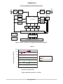
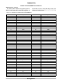
EVBUM2279/D
KAI-4011 / KAI-4021 /
KAI-04022 Imager Board
User's Manual
Description
www.onsemi.com
The
KAI−4011 / KAI−4021 / KAI−04022
Imager
Evaluation Board, referred to in this document as the Imager
Board, is designed to be used as part of a two−board set, used
in conjunction with a Timing Generator Board.
ON Semiconductor offers an Imager Board / Timing
Generator Board package that has been designed and
configured to operate with the KAI−4011 / KAI−4021 /
KAI−04022 Image Sensors.
The Timing Generator Board generates the timing signals
necessary to operate the CCD, and provides the power
required by the Imager Board. The timing signals, in LVDS
format, and the power, are provided to the Imager Board via
the interface connector (J1). In addition, the Timing
Generator Board performs the processing and digitization of
the analog video output of the Imager Board.
The KAI−4011 / KAI−4021 / KAI−04022 Imager Board
has been designed to operate the KAI−4011 / KAI−4021 /
EVAL BOARD USER’S MANUAL
KAI−04022 CCDs with the specified performance at
40 MHz pixel clocking rate and nominal operating
conditions. (See the KAI−4011 / KAI−4021 / KAI−04022
performance specifications for details).
For testing and characterization purposes, the KAI−4011 /
KAI−4021 / KAI−04022 Imager board provides the ability
to adjust many of the CCD bias voltages and CCD clock
level voltages by adjusting potentiometers on the board. The
Imager Board provides the means to modify other device
operating parameters (CCD reset clock pulse width, VSS
bias voltage) by populating components differently on the
board.
INPUT REQUIREMENTS
Table 1. POWER REQUIREMENTS
Power Supplies
Minimum
Typical
Maximum
Units
+5 V_MTR Supply
4.9
5.0
5.1
V
−5 V_MTR Supply
−5.1
1400
mA
−5.0
−4.9
V
200
18
VPLUS Supply
mA
20
21
V
175
−21
VMINUS Supply
mA
−20
−18
V
150
mA
Table 2. SIGNAL LEVEL REQUIREMENTS
Input Signals (LVDS)
Vmin
Vthreshold
Vmax
Units
Comments
H1A (±)
0
±0.1
2.4
V
H1A clock
H1B (±)
0
±0.1
2.4
V
H1B clock
H2A (±)
0
±0.1
2.4
V
H2A clock
H2B (±)
0
±0.1
2.4
V
H2B clock
FDG
0
±0.1
2.4
V
Fast Dump clock
R (±)
0
±0.1
2.4
V
Reset clock
V1 (±)
0
±0.1
2.4
V
V1 clock
V2 (±)
0
±0.1
2.4
V
V2 clock
© Semiconductor Components Industries, LLC, 2014
October, 2014 − Rev. 2
1
Publication Order Number:
EVBUM2279/D
EVBUM2279/D
Table 2. SIGNAL LEVEL REQUIREMENTS
Input Signals (LVDS)
Vmin
Vthreshold
Vmax
Units
Comments
V2B (±)
0
±0.1
2.4
V
V2B clock
V3RD (±)
0
±0.1
2.4
V
V2 Clock 3rd level
VES (±)
0
±0.1
2.4
V
Electronic Shutter
AMP_ENABLE (±)
0
±0.1
2.4
V
Output Amplifier Enable
ARCHITECTURE OVERVIEW
frame to transfer the charge from the photodiodes to the
vertical CCDs.
The following sections describe the functional blocks of
the KAI−4011 / KAI−4021 / KAI−04022 Imager Board
(Refer to Figure 1).
CCD FDG Driver
The Fast Dump Gate (FDG) driver is a transistor that will
switch the voltage on the FDG pin of the CCD from
FDG_LOW to FDG_HIGH during Fast Dump Gate
operation. When not in operation, or when the Fast Dump
Gate feature is not being utilized, the FDG pin of the CCD
is held at FDG_LOW. The FDG_HIGH and FDG_LOW
voltage levels of the FDG driver are set by resistor divider
circuits, and are buffered by operational amplifiers
configured as voltage followers.
Power Filtering and Regulation
Power is supplied to the Imager Board via the J1 interface
connector. The power supplies are de−coupled and filtered
with ferrite beads and capacitors to suppress noise. Voltage
regulators are used to create the +15 V and –15 V supplies
from the VPLUS and VMINUS supplies.
LVDS Receivers / TTL Buffers
LVDS timing signals are input to the Imager Board via the
J1 interface connector. These signals are shifted to TTL
levels before being sent to the CCD clock drivers.
VES Circuit
The pixel rate CCD clock drivers utilize two fast
switching transistors that are designed to translate
TTL−level input clock signals to the voltage levels required
by the CCD. The high level and low level of the CCD clocks
are set by potentiometers.
The quiescent CCD substrate voltage (VSUB) is set by a
potentiometer. For electronic shutter operation, the VES
signal drives a transistor amplifier circuit that AC−couples
the voltage difference between the VPLUS and VMINUS
supplies onto the Substrate voltage. This creates the
necessary potential to clear all charge from the photodiodes,
thereby acting as an electronic shutter to control exposure.
Reset Clock One−Shot (U15; not populated)
CCD Bias Voltages
CCD Pixel−Rate Clock Drivers (H1, H2 & Reset Clocks)
The pulse width of the RESET_CCD clock used to be set
by a programmable One−Shot. The One−Shot was
configured to provide a RESET_CCD clock signal with a
pulse width from 5 ns to 15 ns. Now, the pulse width control
functionality is provided by the KSC−1000 Timing
Generator Board, and the one−shot has been bypassed by
removing U15 and inserting a shorting resistor on pads 1 and
2 of U15.
The CCD bias voltages are set by potentiometers, buffered
by operational amplifiers configured as voltage followers.
The bias voltages are de−coupled at the CCD pin.
CCD Image Sensor
This evaluation board supports the
KAI−4021, and KAI−04022 Image Sensors.
KAI−4011,
Emitter−Follower
The VOUT_CCD signals are buffered using bipolar
junction transistors in the emitter−follower configuration.
These circuits also provide the necessary 5 mA current sink
for the CCD output circuits.
CCD VCLK Drivers
The vertical clock (VCLK) drivers consist of MOSFET
driver IC’s. These drivers are designed to translate the
TTL−level clock signals to the voltage levels required by the
CCD. The high, middle, and low voltage levels of the
vertical clocks are set by potentiometers buffered by
operational amplifiers configured as voltage followers. The
current sources for these voltage levels are high current (up
to 600 mA) transistors. The V2_CCD high level clock
voltage is switched from V_MID to V_HIGH once per
Line Drivers
The buffered VOUT_CCD signals are AC−coupled and
driven from the Imager Board by operational amplifiers in
a non−inverting configuration. The operational amplifiers
are configured to have a gain of 2, to correctly drive 75 W
video coaxial cabling from the SMB connectors.
http://onsemi.com
2
EVBUM2279/D
OPERATIONAL SETTINGS
were correct at the time of this document’s publication, but
may be subject to change; refer to the KAI−4011 /
KAI−4021 / KAI−04022 device specification.
The Imager board is configured to operate the KAI−4011 /
KAI−4021 / KAI−04022 Image Sensors under the following
operating conditions:
DC Bias Voltages
The following voltages are fixed, or adjusted with a
potentiometer as noted. The nominal values listed in Table 3
Table 3. DC BIAS VOLTAGES
Description
Symbol
Min
Nominal
Max
Units
Left Output Amplifier Supply
VDDL
15.0
V
Right Output Amplifier Supply
VDDR
15.0
V
Reset Drain
VRD
ESD Protection
6.7
12.0
ESD
13.5
Potentiometer
1
V
−9.0
Notes
R23
3
V
Substrate
VSUB
8.5
TBD
15.0
V
R18
3
Output Gate Left
VOGL
−7.5
−3.5
−0.4
V
R11
2, 3
Output Gate Right
VOGR
−7.5
−3.5
−0.4
V
R7
2, 3
1. If the CCD is to be operated in single output mode only (VOUT_LEFT) the unused output amplifier supply can be tied to ground to conserve
power by not populating R71, R72 and C76 and by replacing C75 with a 0 W resistor.
2. The Output Gate signals VOGL and VOGR may be controlled independently, or, by installing R28 and R33 and removing R29, may be set
to the same potential, controlled by R11.
3. The Min and Max voltages in the table indicate the imager board potentiometer adjustable voltage range. These values may exceed the
specified CCD operating conditions. See the KAI−4011 / KAI−4021 / KAI−04022 device specification for details.
Clock Voltages
Table 4 were correct at the time of this document’s
publication, but may be subject to change; refer to the
KAI−4011 / KAI−4021 /KAI−04022 device specification.
The following clock voltage levels are fixed, or adjusted
with a potentiometer as noted. The nominal values listed in
Table 4. CLOCK VOLTAGES
Description
Symbol
Level
Min
Nom
Max
Unit
Potentiometer
Notes
Horizontal CCD Clock
Hxx_CCD
Low
−7.5
−4.5
−0.8
V
R147
4
High
0.4
0.5
7.5
V
R127
5
Vx_CCD
Low
−14.0
−9.0
−1.0
V
R40
6
Vx_CCD
Mid
−2.5
−0.0
−0.0
V
R66
7
V2_CCD
High
4.0
9.0
11.0
V
R48
Low
−7.0
−3.5
−1.0
V
R20
High
1.0
5.0
7.0
V
R19
Vertical CCD Clock
Reset Clock
Fast Dump Clock
4.
5.
6.
7.
8.
RESET_CCD
FDG_CCD
Low
−9.0
V
High
5.0
V
The H1A_CCD, H1B_CCD, H2A_CCD, and H2B_CCD low levels are controlled by the same potentiometer (R147).
The H1A_CCD, H1B_CCD, H2A_CCD, and H2B_CCD high levels are controlled by the same potentiometer (R127).
V1_CCD and V2_CCD low levels are controlled by the same potentiometer (R40).
V1_CCD and V2_CCD mid levels are controlled by the same potentiometer (R66).
FDG is used to flush the device when operated in Still Mode.
http://onsemi.com
3
8
EVBUM2279/D
BLOCK DIAGRAM AND PERFORMANCE DATA
J3
SMB
J2
SMB
LINE
DRIVER
EMITTER
FOLLOWER
EMITTER
FOLLOWER
V3RD
DRIVER
V2
DRIVER
LINE
DRIVER
(optional)
VOUT LEFT
VOUT RIGHT
CCD SENSOR
RCLK
DRIVER
RCLK
1 SHOT
FDG CKT
V1
DRIVER
VES CKT
H1A
DRIVER
H2A
DRIVER
H1B
DRIVER
H2B
DRIVER
LVDS TO TTL BUFFERS
+15 V
REGULATOR
LVDS RECEIVERS
−15 V
REGULATOR
J1 BOARD INTERFACE CONNECTOR
Figure 1. KAI−4011 / KAI−4021 / KAI−04022 Imager Board Block Diagram
LINEARITY
SIGNAL MEAN (ELECTRONS)
100000
10000
1000
MEASURED
100
FIT
10
%DEVIATION FROM FIT
1
0.1
0.01
0.1
1
10
INTEGRATION TIME (SECONDS)
Figure 2. Measured Performance − Linearity
http://onsemi.com
4
EVBUM2279/D
Photon Transfer
100
Noise (A/D counts)
Slope = el/Adu = 9.29 electrons
Noise floor = 3.65 counts (33.9
electrons)
10
LVSAT = 30220 electrons
VSAT = 32980 electrons
1
10
100
1000
10000
100000
Signal Mean (Electrons)
Figure 3. Measured Performance − Dynamic Range and Noise Floor
http://onsemi.com
5
EVBUM2279/D
CONNECTOR ASSIGNMENTS AND PINOUTS
SMB Connectors J2 and J3
75 W should be used to connect the imager board to the
Timing Generator Board to match the series and terminating
resistors used on these boards.
The emitter−follower buffered CCD_VOUT signals are
driven from the Imager Board via the SMB connectors J2
and J3. Coaxial cable with a characteristic impedance of
Table 5. J1 INTERFACE CONNECTOR PIN ASSIGNMENTS
Pin
Signal
Pin
Signal
1
N.C.
2
N.C.
3
AGND
4
AGND
5
VES+
6
VES−
7
AGND
8
AGND
9
FDG+
10
FDG−
11
AGND
12
AGND
13
V3RD+
14
V3RD−
15
AGND
16
AGND
17
V2B+
18
V2B−
19
AGND
20
AGND
21
V2+
22
V2−
23
AGND
24
AGND
25
V1+
26
V1−
27
AGND
28
AGND
29
R+
30
R−
31
AGND
32
AGND
33
H2B+
34
H2B−
35
AGND
36
AGND
37
H2A+
38
H2A−
39
AGND
40
AGND
41
H1B+
42
H1B−
43
AGND
44
AGND
45
H1A+
46
H1A−
47
N.C.
48
N.C.
49
AGND
50
AGND
51
N.C.
52
N.C.
53
VMINUS_MTR
54
VMINUS_MTR
55
N.C.
56
N.C.
57
AGND
58
AGND
59
AMP_ENABLE+
60
AMP_ENABLE−
61
−5 V_MTR
62
−5 V_MTR
63
N.C.
64
N.C.
65
AGND
66
AGND
67
N.C.
68
N.C.
69
+5 V_MTR
70
+5 V_MTR
71
N.C.
72
N.C.
73
AGND
74
AGND
75
N.C.
76
N.C.
77
VPLUS_MTR
78
VPLUS_MTR
79
N.C.
80
N.C.
http://onsemi.com
6
EVBUM2279/D
Warnings and Advisories
Ordering Information
ON Semiconductor is not responsible for customer
damage to the Imager Board or Imager Board electronics.
The customer assumes responsibility and care must be taken
when probing, modifying, or integrating the
ON Semiconductor Evaluation Board Kits.
When programming the Timing Board, the Imager Board
must be disconnected from the Timing Board before power
is applied. If the Imager Board is connected to the Timing
Board during the reprogramming of the Altera PLD, damage
to the Imager Board will occur.
Purchasers of an Evaluation Board Kit may, at their
discretion, make changes to the Timing Generator Board
firmware. ON Semiconductor can only support firmware
developed by, and supplied by, ON Semiconductor. Changes
to the firmware are at the risk of the customer.
Please address all inquiries and purchase orders to:
Truesense Imaging, Inc.
1964 Lake Avenue
Rochester, New York 14615
Phone:
(585) 784−5500
E−mail:
[email protected]
ON Semiconductor reserves the right to change any
information contained herein without notice. All
information furnished by ON Semiconductor is believed to
be accurate.
ON Semiconductor and the
are registered trademarks of Semiconductor Components Industries, LLC (SCILLC) or its subsidiaries in the United States and/or other countries.
SCILLC owns the rights to a number of patents, trademarks, copyrights, trade secrets, and other intellectual property. A listing of SCILLC’s product/patent coverage may be accessed
at www.onsemi.com/site/pdf/Patent−Marking.pdf. SCILLC reserves the right to make changes without further notice to any products herein. SCILLC makes no warranty, representation
or guarantee regarding the suitability of its products for any particular purpose, nor does SCILLC assume any liability arising out of the application or use of any product or circuit, and
specifically disclaims any and all liability, including without limitation special, consequential or incidental damages. “Typical” parameters which may be provided in SCILLC data sheets
and/or specifications can and do vary in different applications and actual performance may vary over time. All operating parameters, including “Typicals” must be validated for each
customer application by customer’s technical experts. SCILLC does not convey any license under its patent rights nor the rights of others. SCILLC products are not designed, intended,
or authorized for use as components in systems intended for surgical implant into the body, or other applications intended to support or sustain life, or for any other application in which
the failure of the SCILLC product could create a situation where personal injury or death may occur. Should Buyer purchase or use SCILLC products for any such unintended or
unauthorized application, Buyer shall indemnify and hold SCILLC and its officers, employees, subsidiaries, affiliates, and distributors harmless against all claims, costs, damages, and
expenses, and reasonable attorney fees arising out of, directly or indirectly, any claim of personal injury or death associated with such unintended or unauthorized use, even if such claim
alleges that SCILLC was negligent regarding the design or manufacture of the part. SCILLC is an Equal Opportunity/Affirmative Action Employer. This literature is subject to all applicable
copyright laws and is not for resale in any manner.
PUBLICATION ORDERING INFORMATION
LITERATURE FULFILLMENT:
Literature Distribution Center for ON Semiconductor
P.O. Box 5163, Denver, Colorado 80217 USA
Phone: 303−675−2175 or 800−344−3860 Toll Free USA/Canada
Fax: 303−675−2176 or 800−344−3867 Toll Free USA/Canada
Email: [email protected]
N. American Technical Support: 800−282−9855 Toll Free
USA/Canada
Europe, Middle East and Africa Technical Support:
Phone: 421 33 790 2910
Japan Customer Focus Center
Phone: 81−3−5817−1050
http://onsemi.com
7
ON Semiconductor Website: www.onsemi.com
Order Literature: http://www.onsemi.com/orderlit
For additional information, please contact your local
Sales Representative
EVBUM2279/D