1
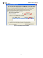
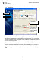
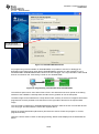
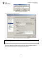
SmartRF™ Flash Programmer
User Manual
SWRU069G
SmartRF™ Flash Programmer
SWRU069G
Table of contents
1
2
3
4
5
5.1
INTRODUCTION ........................................................................................................................................3
ABOUT THIS MANUAL ............................................................................................................................3
DEFINITIONS .............................................................................................................................................3
INSTALLATION. ........................................................................................................................................4
PROGRAMMING USING THE GUI VERSION .....................................................................................5
PROGRAM CCXXX SOC OR MSP430 DEVICES. ...............................................................................................5
5.1.1
5.1.2
5.2.1
5.2.2
5.2.3
System on chip ........................................................................................................................................................................................ 6
MSP430 Programming ......................................................................................................................................................................... 11
PROGRAM EVALUATION BOARD ...................................................................................................................12
USB MCU firmware update.................................................................................................................................................................. 12
Automatic Firmware update of the Evaluation Board. ......................................................................................................................... 13
EB bootloader ...................................................................................................................................................................................... 15
6
6.1
6.2
COMMAND LINE INTERFACE.............................................................................................................17
OPTIONS ........................................................................................................................................................17
PLUG-IN TO IAR WORKBENCH......................................................................................................................17
6.2.1
6.2.2
Setup ..................................................................................................................................................................................................... 17
Use ....................................................................................................................................................................................................... 18
7
8
9
INSTALLED HEX FILES .........................................................................................................................21
TROUBLESHOOTING .............................................................................................................................21
DOCUMENT HISTORY ...........................................................................................................................22
5.2
2/22
SmartRF™ Flash Programmer
SWRU069G
1
Introduction
This is the user manual for the SmartRF Flash Programmer.
The Flash Programmer can be used to program the flash memory in Texas Instruments Low Power RF
System on Chips and for programming the flash memory of MSP430 devices via the MSP-FET430UIF
and the eZ430 dongle.
For IEEE 802.15.4 compliant devices (e.g. CC2530) and Bluetooth® low energy devices (e.g. CC2540)
the Flash Programmer support reading and writing the IEEE/MAC address.
In addition, the Flash Programmer can be used for upgrading the firmware on the SmartRF04EB,
SmartRF05EB, CC Debugger and CC2430DB.
2
About this manual
This manual covers the use of the Flash programmer, both the GUI version and the -Command Line
Interface.
The manual describes the most common functions and options available. Chapter 5.2 will describe how
to use the Command Line Interface of the Flash Programmer from IAR Embedded Workbench to
perform post-build operations like flash programming.
The Flash Programmer has functionality to program the USB MCU found on SmartRF04EB and
CC2430DB through the Silicon Laboratories serial adapter EC2. This is not covered in this manual.
3
Definitions
CC Debugger
The CC Debugger can be used as interface to program SoC’s
mounted on Battery Boards and to update the USB MCU on
SmartRF05EB.
CLI
Command Line Interface
Factory firmware
The firmware that is supplied programmed into the USB MCU
from the factory. This firmware supports SmartRF® Studio
operation as well as a stand-alone PER tester.
GUI
Graphical User Interface
SmartRF®04DK
A collective term used for all development kits for the
SmartRF®04 platform, i.e. CC2510DK and CC2430ZDK
SmartRF®05DK
A collective term used for all development kits for the
SmartRF05 platform, i.e. CC2520DK
USB MCU
The Silicon Labs C8051F320 MCU used to provide a USB
interface on the SmartRF®04EB and CC2430DB.
The CC2511 MCU used to provide a USB interface on the
SmartRF05EB.
3/22
SmartRF™ Flash Programmer
SWRU069G
4
Installation.
Download and unpack the zip file from the TI web page: http://www.ti.com/tool/flash-programmer
Double click on “Setup_SmartRFProgr_x.x.x.exe” file to start the installation. Follow the instructions on
the screen.
Note:
The installation of SmartRF Flash Programmer must be executed with administrator privileges.
For Windows Vista and Windows 7 a “User Access Control” dialog will appear when starting the
installer. If the user has administrator privileges, click on the “yes” button to continue installation. If the
user doesn’t have administrator privileges, a user id and password with these privileges must be
entered.
4/22
SmartRF™ Flash Programmer
SWRU069G
5
Programming Using the GUI Version
The Graphical User Interface operates in two different user modes: One for programming of System on
Chip modules and one for programming of the Evaluation Boards MCU.
5.1
Program CCxxx SoC or MSP430 devices.
Figure 1 shows the user mode for programming of System on Chip modules. Two types of modules are
supported.
MSP430 tab
used to program
MSP430 MCU’s.
System on Chip
tab. Used to
program CCxxxx
SoC.
Figure 1, Program CCxxxx SoC or MSP430
“System on Chip” is used to program Texas Instruments SOC’s e.g. CC1110, CC2430, CC2510, and
CC2530. The use of this tab is described in chapter 5.1.1.
“MSP430” is used to program the MSP430 MCU used in various RF development kits. Further details
are described in chapter 5.1.2.
5/22
SmartRF™ Flash Programmer
SWRU069G
5.1.1
System on chip
Device list
Chapter 5.1.1.1
IEEE address
(only CC2430)
Chapter 5.1.1.4
Actions
Chapter 5.1.1.2
Flash lock
Chapter 5.1.1.3
Figure 2: System on Chip window
5.1.1.1
Device list:
The device list show all currently connected System on Chip devices. Note that when the System on
Chip tab is selected, any Evaluation Board without a System on Chip EM connected will not be
displayed.
If more than one chip is connected the one selected (marked blue) in this window is the one that will be
programmed.
6/22
SmartRF™ Flash Programmer
SWRU069G
5.1.1.2
Actions:
There are six different actions that can be performed on the Texas Instruments SoC. To perform an
action, select one and then press the “Perform actions” button.
The progress bar and output window at the bottom will output the progress and result of the action.
The six actions are:
Erase
This action will erase the flash memory of the selected SoC.
Erase and program
Will erase the flash memory of the selected SoC and then program it with the .hex file selected in
the “Flash image” field.
Erase, program and verify
Same as “Erase and program”, but after the programming the content of the flash will be read
back and compared with the .hex file. This will detect errors during programming or errors caused
by damaged flash. It is therefore recommended to always verify after programming.
Append and verify
This action will write the contents of the hex file given in the “Flash image” field, to the selected
SoC without erasing the Flash first. Note that all the Flash written to must read 0xFF (be erased)
before programming starts. Feature is useful when a program is divided into more that one hex
file.
This action uses debug commands to read from the Flash, which means that if the debug
commands are blocked on the chip, it is impossible to perform this action.
Verify against hex-file
This action will compare the contents of the Flash with a .hex file given in the “Flash image” field.
Note that the function only verifies that the contents of the .hex file is present in the Flash, it does
not check if there is anything additional written in the Flash.
This action uses debug commands to read from the Flash, which means that if the debug
commands are blocked on the chip, it is impossible to perform this action.
Read into hex-file
This action will read the entire content of the Flash and then write it to the hex-file given in the
“Flash image” field.
Note that the hex-file given in the “Flash image” field will be overwritten.
This action uses debug commands to read from the Flash, which means that if the debug
commands are blocked on the chip, it is impossible to perform this action.
7/22
SmartRF™ Flash Programmer
SWRU069G
5.1.1.3
Flash lock:
When programming a chip it is possible to apply the different flash lock and debug command lock
options that are supported by the chip. These fields will change depending on the chip type selected in
the device list. Please refer to the datasheet for the different chip types for a description of these lock
features.
Note that if the debug command lock is set, it is impossible to use most of the debug commands on the
chip. E.g. the flash may no longer be read out.
CC11xx, CC25xx and CC24xx:
For these devices it is possible to write protect all pages or the upper part of the page numbers.
Figure 3, Write protect CC243x
CC253x and CC2540:
For these devices it is possible to write protect each page of the flash image. The input field “Write
protect” should be given as shown in Figure 4, Write protect CC2530. The pages to be write protected
can be given separated by a comma. It is also possible to specify a range of pages.
Figure 4, Write protect CC2530
5.1.1.4
IEEE 802.15.4 address / general change field:
The input fields for the IEEE address depend on the connected RF Device.
Figure 5: IEEE address for ZigBee SoC (CC2430/31)
Figure 6: IEEE address for ZigBee SoC (CC2530/31)
Figure 7: Change field for non ZigBee SoC
8/22
SmartRF™ Flash Programmer
SWRU069G
IEEE address on ZigBee devices like CC2430/31
On a CC243x the IEEE address is stored in the last 8 bytes of the flash. E.g. the placement is
different depending on the size of the Flash. See Table 1 below.
Chip type
IEEE address start
IEEE address end
CC243xF128
0x1FFF8
0x1FFFF
CC243xF64
0xFFF8
0xFFFF
CC243xF32
0x7FF8
0x7FFF
Table 1: Placement of IEEE address
To read the IEEE address from a chip select the appropriate Chip type (e.g. F-128) and push the
“Read IEEE” button.
To write the IEEE address to a chip, manually write the address into the IEEE field (hexadecimal,
with a space between each byte) and then push the “Write IEEE address” button.
Writing the IEEE address will fail if the flash is write-protected, or the debug command lock is set.
If the “Retain IEEE address when reprogramming the chip” is checked the IEEE address is
preserved when a new program is written to the chip with the “Erase and program” or “Erase,
program and verify” action. This is however not possible if the debug command lock is set on the
chip before the programming starts.
IEEE address on ZigBee devices like CC2530/31
For CC253x it is possible to have two IEEE addresses programmed in flash. The Primary address
is programmed in the Information Page and can only be read. The address is preprogrammed in
factory.
The secondary IEEE address, which is optional (used when the address in the information page is
not used), is stored at the end of the flash. The last 16 bytes is used for lock bits and the IEEE
address is stored in the last 8 bytes before the lock bits.
Chip type
IEEE address start
IEEE address end
CC253xF256
0x3FFE8
0x3FFEF
CC253xF128
0x1FFE8
0x1FFEF
CC253xF64
0xFFE8
0xFFEF
CC253xF32
0x7FE8
0x7FEF
To read the IEEE address, select either Primary or Secondary and push the “Read IEEE” button.
Only the secondary IEEE address can be written. All the other rules are the same as described
above for CC243x.
Change Field on non ZigBee devices
The intention of this field is to provide an easy and quick way to give a unique address to the chip
when programming it. It gives the user the possibility to change any number of bytes at any
location in the program read from the hex file, before it is written to the chip.
When “Change” is checked, input the start address, e.g. the first byte that should be changed into
the first field.
Then the new values are written into the rightmost field (hexadecimal, with a space between each
byte)
When “Erase and program” or “Erase, program and verify” action is performed, the bytes at the
given address from the hex file are replaced with those written by the user before the chip is
programmed. The hex file itself is not changed.
9/22
SmartRF™ Flash Programmer
SWRU069G
5.1.1.5
View Information Page
To view the information page click on the “View Info Page” button
shown at the left side (Only applicable for CC253x and CC254x).
The Information Page
is a read-only region
that stores various
device information.
10/22
SmartRF™ Flash Programmer
SWRU069G
5.1.2
MSP430 Programming
The Device Name
will indicate the
MSP430 MCU
device name
Port Name indicate if
Virtual serial port
(COM) or Human
Interface Device
(HID) will be used for
the connected
device.
Read/Write of the
IEEE address is only
applicable for
devices where the
flash location have
been defined.
Status field
Figure 8: MSP430 Programming.
Figure 8 show the tab used for programming of the MSP430 MCU. The device can be connected via
the USB-Debug-Interface (MSP-FET430UIF) or via the eZ430 USB dongle. The figure show both
cases. Devices connected with the MSP-FET430UIF will appear as a COM port. In this case it is
COM47. For eZ430 connected devices it will be seen as both a HID port and COM port.
When the device is connected via the USB interface, it could take a few seconds before the device
appear in the device list.
The status of all actions will be given in the Status field at the bottom of the window. An attempt to
program a hex file build for another MCU family will be detected and reported in the Status field.
The Firmware version of the MSP-FET430UIF will be checked automatically when a device is
connected. If the FW version does not match the PC Software version, a message will be given and the
user must choose whether or not to update the FW. The update will be performed automatically if the
user chooses to update the FW.
11/22
SmartRF™ Flash Programmer
SWRU069G
5.2
Program Evaluation Board
Firmware
revision
number
Figure 9, Programming of the Evaluation Board
“EB application (USB)” is used when updating the USB MCU found on SmartRF04EB, SmartRF05EB,
CC Debugger and CC2430DB. The use of this tab is described in chapter 5.2.1.
“EB application (serial)” can be used in stead of the “EB application (USB)” to update the USB MCU on
SmartRF04EB. This setup requires the EC2 serial adapter from Silab. For the rest it has the same
functionality as the “EB application (USB)”.
“EB bootloader” is used to update the bootloader on SmartRF04EB, SmartRF05EB, CC Debugger and
CC2430DB. Further details are described in chapter 5.2.3.
5.2.1
USB MCU firmware update
Figure 9 show the “EB application (USB)” tab. It provides the possibility to update the firmware on an
Evaluation Board using only a USB cable. No additional programmer is necessary. When a
SmartRF04EB, SmartRF05EB, CC Debugger or CC2430DB is connected it will appear in the device
list. In the rightmost column the revision number of the current firmware can be read.
Note that the update procedure is different for SmartRF04EB and CC2430DB. However the hex file
used, (fw400.hex), is identical for the two products.
SmartRF05EB and CC Debugger uses a different hex file specially build for the USB MCU (CC2511)
12/22
SmartRF™ Flash Programmer
SWRU069G
5.2.1.1
Updating SmartRF04EB/SmartRF05EB USB MCU firmware
1. Remove any CCxxxxEM module and all external equipment connected to the Evaluation Board.
2. Connect the USB cable to the Evaluation Board and turn it on, it should appear in the Device
list with “Chip type” N/A.
3. Browse to the correct flash image (e.g. fw0400.hex for SmartRF04EB)
4. Choose the “Erase, program and verify”
5. Push “Perform actions”.
6. The status indicator at the bottom will show the progress and when completed the text “EB
firmware update OK” will appear.
5.2.1.2
Updating CC2430DB USB MCU firmware
1. Remove all jumpers on P5.
2. Connect pin 9 and 10 on P4 (USB deb) together.
3. Connect the USB cable to the CC2430DB and turn it on, it should appear in the Device list with
“Chip type”, “EB type” and “EB firmware ID” set to N/A.
4. Browse to the correct flash image (e.g. fw400.hex)
5. Choose the “Erase, program and verify”
6. Push “Perform actions”.
7. The status indicator at the bottom will show the progress and when completed the text “EB
firmware update OK” will appear.
8. Remove jumper on pin 9-10 on P4, and mount jumpers on P5.
Note: After the programming is finished it takes a few seconds before the device appear in the device
list. This is due to timing constrains on the USB bus after programming and reset of the device.
5.2.2
Automatic Firmware update of the Evaluation Board.
The firmware can be updated automatically with the latest version. The latest version of the firmware is
installed together with any of the SmartRF Tools. When the Evaluation Board is connected to the USB
port, the flash programmer will compare the current firmware version with the version found in the hex
files installed together with the flash programmer. If current firmware is found to be an old version, this
will be indicated as shown in Figure 10.
The firmware is of
an old revision.
The “Update EB
Firmware” button
is enabled
Figure 10, Old firmware indication
There will also be a popup dialog with information about how to update the EB Firmware. See Figure 11
13/22
SmartRF™ Flash Programmer
SWRU069G
Figure 11, Popup dialog for old EB firmware.
14/22
SmartRF™ Flash Programmer
SWRU069G
5.2.3
EB bootloader
The bootloader of the different Evaluation Boards can be updated from the “EB bootloader” tab.
5.2.3.1
SmartRF04EB
Select Device
Select Serial Port
The ID Number
should be given as 4
decimal digits.
The ID Number can
be automatically
incremented when
programming has
finished. “Ready for
next board”.
Figure 12, SmartRF04EB Bootloader
To program the bootloader on SmartRF04EB it is required to use the Serial Adapter (EC2) from Silabs.
Select Serial port and flash image. The flash image can be selected from a drop down list with a history
of the last 10 images that has been programmed. It is also possible to use the button on the right side to
browse for the required flash image
Specify the board identification (ID Number) and select the actions “Erase and program” or “Erase,
program and verify”.
Click the “Perform actions” button to start programming. Status will be displayed in the field below the
button.
The action “Verify against hex-file” can be used to check current image on the USB MCU with the given
hex file.
15/22
SmartRF™ Flash Programmer
SWRU069G
5.2.3.2
SmartRF05EB
The Programmer
should be listed here.
Figure 13, SmartRF05EB bootloader
For programming of the bootloader on SmartRF05EB, it is possible to use the CC Debugger as
illustrated on the image shown when Device SmartRF05EB is selected. It is also possible to use a
SmartRF04EB or SmartRF05EB board instead of the CC Debugger. The 10 pin flat ribbon cable should
then be connected on the “SoC Debug” header on the SmartRF0xEB.
Programmer
Device to be programmed
Figure 14, Programming of bootloader with SmartRF04EB
The interface speed can be set to either Fast or Slow. This determines the clock speed on the debug
interface of the USB MCU. Normally there shouldn’t be any problem to use the fast speed.
The flash image can be selected from a drop down list with a history of the last 10 images that has been
programmed. It is also possible to use the button on the right side to browse for the required flash
image.
The connected CC Debugger or SmartRF04EB board should be visible in the list of connected devices.
The “Chip type” should be CC2511. Select the required device.
Specify the board identification (ID Number) and select the actions “Erase and program” or “Erase,
program and verify”.
Click the “Perform actions” button to start programming. Status will be displayed in the field below the
button.
16/22
SmartRF™ Flash Programmer
SWRU069G
6
6.1
Command Line Interface
Options
To get all available options in the command line interface, run the SmartRFProgConsole.exe in a
command window without any parameters/arguments. A list of all available options will then be printed
out. These options are the same as the ones available in the GUI version of the Flash programmer.
Please refer to chapter 4 for a description of these.
6.2
Plug-in to IAR Workbench
The command line interface can be integrated in the IAR Workbench. To setup IAR with this feature
follow the instructions below.
6.2.1 Setup
Start IAR Workbench and choose “Configure Tools…”, from the Tools menu, Figure 15.
Figure 15: Tools Menu
Press “New”, and add the information present in Table 2, see Figure 16.
Field
Value
Menu Text:
FlashProgram
Command:
C:\Program Files\Texas Instruments\SmartRF Tools\Flash
1
Programmer\bin\SmartRFProgConsole.exe
Argument:
S() EPV F=$TARGET_PATH$ K(0)
Table 2: Flash Programmer Setup
1
Insert the complete path to the Command Line Flash Programmer
17/22
SmartRF™ Flash Programmer
SWRU069G
Figure 16: Configure Tools
6.2.2
Use
After setup, a new target is placed on the Tools menu.
Figure 17: Using Flash Programmer from IAR Workbench
Setup your project to generate hex file as primary output (Figure 19), compile and link, and choose
“Flash Program” from the Tools menu. A command line window will be displayed, Figure 18. After the
“S” option an empty parenthesize is present. If this parenthesize is empty, the first available
development card is used. If more than one development card is connected, fill in the ID number for the
card you want to use in the empty parenthesize.
The K(0) option will retain the IEEE address while programming.
Use K(0) on CC2430F128, K(1) on CC2430F64 and K(2) on CC2430F32.
If the K option is removed the IEEE address is not retained.
The “EPV” option is for “Erase, program and verify”
18/22
SmartRF™ Flash Programmer
SWRU069G
Figure 18: Command Line Window
Press OK and the hex file will be downloaded.
Figure 19: Generate HEX file as primary output
To produce a hex file for banked code, please see the manual named “SWRU038 IAR User Manual”
available from www.ti.com.
Note that if you only select the HEX file as output from the linker, you cannot debug this particular
image. To have both the hex file and the debug file output, select “Debug information for C-SPY” and
“Allow C-SPY-specific extra output file”. Then select the “Extra Output” tab.
19/22
SmartRF™ Flash Programmer
SWRU069G
Select “Generate extra output file” and specify name of the .hex file.
20/22
SmartRF™ Flash Programmer
SWRU069G
7
Installed hex files
After installation of the Flash Programmer, a few hex files have been installed. The typical location of
these files will be:
C:\Program Files\Texas Instruments\SmartRF Tools\Firmware
For each device there will be a subfolder with the latest firmware version:
.\SmartRF04EB \srf04eb_bootloader.hex
\cc2430db_bootloader.hex
\fw0400.hex
SmartRF04EB bootloader.
CC2430DB bootloader
SmartRF04EB application.
.\SmartRF05EB \usb_bootloader_srf05eb.hex
\cebal_fw_srf05eb.hex
SmartRF05EB bootloader.
SmartRF05EB application.
.\CC Debugger \usb_bootloader_srf05dbg.hex CC Debugger bootloader.
\cebal_fw_srf05dbg.hex
CC Debugger application.
.\TrxEB \usb_bootloader_trxeb.hex
\cebal_fw_trxeb.hex
8
TrxEB bootloader.
TrxEB application.
Troubleshooting
This section contains troubleshooting for the SmartRF Flash Programmer. If this section does not
answer your question, try the user’s guide of your device or evaluation board, or, search the Texas
Instruments E2E forum http://www.ti.com/e2e.
Q1
I have two EBs with the same EB ID, and I’m unable to use them together. What do I do?
A1
Two EBs with the same EB ID cause a driver conflict. The solution is to resurrect one of the EBs
and give it a new EB ID. Here, it is assumed that the EBs is two CC Debuggers, but this applies
to SmartRF05EB as well.
1. Connect one CC Debugger to your computer
2. Connect the CC Debugger you want to resurrect to a separate power source (e.g. another
computer or a USB charger).
3. Use SmartRF Flash Programmer to resurrect the CC Debugger as described in the CC
Debugger’s User’s guide.
For details on resurrecting other EBs, do step 1 and 2 above and follow the resurrection process
in the respective EB’s User’s Guide.
21/22
SmartRF™ Flash Programmer
SWRU069G
9
Document history
Revision
Date
Description/Changes
G
2014-01-15
Added Troubleshooting chapter. Mapped revision numbers in this
table to the TI literature revision number.
F
2012-01-18
Added information about the installation.
E
2010-12-09
Updated with the changes of the SmartRF Flash Programmer version
1.10.x.
D
2009-02-11
New version with support for CC2530 and the CC Debugger.
C
2007-12-27
New version with support for SmartRF05EB and MSP430
B
2007-09-19
Update of images and description of hex files added.
A
2006-05-16
Minor changes
1.1
2006-02-16
Changed layout
1.0
2005-12-21
Initial release
22/22
EVALUATION BOARD/KIT/MODULE (EVM) ADDITIONAL TERMS
Texas Instruments (TI) provides the enclosed Evaluation Board/Kit/Module (EVM) under the following conditions:
The user assumes all responsibility and liability for proper and safe handling of the goods. Further, the user indemnifies TI from all claims
arising from the handling or use of the goods.
Should this evaluation board/kit not meet the specifications indicated in the User’s Guide, the board/kit may be returned within 30 days from
the date of delivery for a full refund. THE FOREGOING LIMITED WARRANTY IS THE EXCLUSIVE WARRANTY MADE BY SELLER TO
BUYER AND IS IN LIEU OF ALL OTHER WARRANTIES, EXPRESSED, IMPLIED, OR STATUTORY, INCLUDING ANY WARRANTY OF
MERCHANTABILITY OR FITNESS FOR ANY PARTICULAR PURPOSE. EXCEPT TO THE EXTENT OF THE INDEMNITY SET FORTH
ABOVE, NEITHER PARTY SHALL BE LIABLE TO THE OTHER FOR ANY INDIRECT, SPECIAL, INCIDENTAL, OR CONSEQUENTIAL
DAMAGES.
Please read the User's Guide and, specifically, the Warnings and Restrictions notice in the User's Guide prior to handling the product. This
notice contains important safety information about temperatures and voltages. For additional information on TI's environmental and/or safety
programs, please visit www.ti.com/esh or contact TI.
No license is granted under any patent right or other intellectual property right of TI covering or relating to any machine, process, or
combination in which such TI products or services might be or are used. TI currently deals with a variety of customers for products, and
therefore our arrangement with the user is not exclusive. TI assumes no liability for applications assistance, customer product design,
software performance, or infringement of patents or services described herein.
REGULATORY COMPLIANCE INFORMATION
As noted in the EVM User’s Guide and/or EVM itself, this EVM and/or accompanying hardware may or may not be subject to the Federal
Communications Commission (FCC) and Industry Canada (IC) rules.
For EVMs not subject to the above rules, this evaluation board/kit/module is intended for use for ENGINEERING DEVELOPMENT,
DEMONSTRATION OR EVALUATION PURPOSES ONLY and is not considered by TI to be a finished end product fit for general consumer
use. It generates, uses, and can radiate radio frequency energy and has not been tested for compliance with the limits of computing
devices pursuant to part 15 of FCC or ICES-003 rules, which are designed to provide reasonable protection against radio frequency
interference. Operation of the equipment may cause interference with radio communications, in which case the user at his own expense will
be required to take whatever measures may be required to correct this interference.
General Statement for EVMs including a radio
User Power/Frequency Use Obligations: This radio is intended for development/professional use only in legally allocated frequency and
power limits. Any use of radio frequencies and/or power availability of this EVM and its development application(s) must comply with local
laws governing radio spectrum allocation and power limits for this evaluation module. It is the user’s sole responsibility to only operate this
radio in legally acceptable frequency space and within legally mandated power limitations. Any exceptions to this are strictly prohibited and
unauthorized by Texas Instruments unless user has obtained appropriate experimental/development licenses from local regulatory
authorities, which is responsibility of user including its acceptable authorization.
For EVMs annotated as FCC – FEDERAL COMMUNICATIONS COMMISSION Part 15 Compliant
Caution
This device complies with part 15 of the FCC Rules. Operation is subject to the following two conditions: (1) This device may not cause
harmful interference, and (2) this device must accept any interference received, including interference that may cause undesired operation.
Changes or modifications not expressly approved by the party responsible for compliance could void the user's authority to operate the
equipment.
FCC Interference Statement for Class A EVM devices
This equipment has been tested and found to comply with the limits for a Class A digital device, pursuant to part 15 of the FCC Rules.
These limits are designed to provide reasonable protection against harmful interference when the equipment is operated in a commercial
environment. This equipment generates, uses, and can radiate radio frequency energy and, if not installed and used in accordance with the
instruction manual, may cause harmful interference to radio communications. Operation of this equipment in a residential area is likely to
cause harmful interference in which case the user will be required to correct the interference at his own expense.
FCC Interference Statement for Class B EVM devices
This equipment has been tested and found to comply with the limits for a Class B digital device, pursuant to part 15 of the FCC Rules.
These limits are designed to provide reasonable protection against harmful interference in a residential installation. This equipment
generates, uses and can radiate radio frequency energy and, if not installed and used in accordance with the instructions, may cause
harmful interference to radio communications. However, there is no guarantee that interference will not occur in a particular installation. If
this equipment does cause harmful interference to radio or television reception, which can be determined by turning the equipment off and
on, the user is encouraged to try to correct the interference by one or more of the following measures:
• Reorient or relocate the receiving antenna.
• Increase the separation between the equipment and receiver.
• Connect the equipment into an outlet on a circuit different from that to which the receiver is connected.
• Consult the dealer or an experienced radio/TV technician for help.
For EVMs annotated as IC – INDUSTRY CANADA Compliant
This Class A or B digital apparatus complies with Canadian ICES-003.
Changes or modifications not expressly approved by the party responsible for compliance could void the user’s authority to operate the
equipment.
Concerning EVMs including radio transmitters
This device complies with Industry Canada licence-exempt RSS standard(s). Operation is subject to the following two conditions: (1) this
device may not cause interference, and (2) this device must accept any interference, including interference that may cause undesired
operation of the device.
Concerning EVMs including detachable antennas
Under Industry Canada regulations, this radio transmitter may only operate using an antenna of a type and maximum (or lesser) gain
approved for the transmitter by Industry Canada. To reduce potential radio interference to other users, the antenna type and its gain should
be so chosen that the equivalent isotropically radiated power (e.i.r.p.) is not more than that necessary for successful communication.
This radio transmitter has been approved by Industry Canada to operate with the antenna types listed in the user guide with the maximum
permissible gain and required antenna impedance for each antenna type indicated. Antenna types not included in this list, having a gain
greater than the maximum gain indicated for that type, are strictly prohibited for use with this device.
Cet appareil numérique de la classe A ou B est conforme à la norme NMB-003 du Canada.
Les changements ou les modifications pas expressément approuvés par la partie responsable de la conformité ont pu vider l’autorité de
l'utilisateur pour actionner l'équipement.
Concernant les EVMs avec appareils radio
Le présent appareil est conforme aux CNR d'Industrie Canada applicables aux appareils radio exempts de licence. L'exploitation est
autorisée aux deux conditions suivantes : (1) l'appareil ne doit pas produire de brouillage, et (2) l'utilisateur de l'appareil doit accepter tout
brouillage radioélectrique subi, même si le brouillage est susceptible d'en compromettre le fonctionnement.
Concernant les EVMs avec antennes détachables
Conformément à la réglementation d'Industrie Canada, le présent émetteur radio peut fonctionner avec une antenne d'un type et d'un gain
maximal (ou inférieur) approuvé pour l'émetteur par Industrie Canada. Dans le but de réduire les risques de brouillage radioélectrique à
l'intention des autres utilisateurs, il faut choisir le type d'antenne et son gain de sorte que la puissance isotrope rayonnée équivalente
(p.i.r.e.) ne dépasse pas l'intensité nécessaire à l'établissement d'une communication satisfaisante.
Le présent émetteur radio a été approuvé par Industrie Canada pour fonctionner avec les types d'antenne énumérés dans le manuel
d’usage et ayant un gain admissible maximal et l'impédance requise pour chaque type d'antenne. Les types d'antenne non inclus dans
cette liste, ou dont le gain est supérieur au gain maximal indiqué, sont strictement interdits pour l'exploitation de l'émetteur.
SPACER
SPACER
SPACER
SPACER
SPACER
SPACER
SPACER
SPACER
【Important Notice for Users of EVMs for RF Products in Japan】
】
This development kit is NOT certified as Confirming to Technical Regulations of Radio Law of Japan
If you use this product in Japan, you are required by Radio Law of Japan to follow the instructions below with respect to this product:
1.
2.
3.
Use this product in a shielded room or any other test facility as defined in the notification #173 issued by Ministry of Internal Affairs and
Communications on March 28, 2006, based on Sub-section 1.1 of Article 6 of the Ministry’s Rule for Enforcement of Radio Law of
Japan,
Use this product only after you obtained the license of Test Radio Station as provided in Radio Law of Japan with respect to this
product, or
Use of this product only after you obtained the Technical Regulations Conformity Certification as provided in Radio Law of Japan with
respect to this product. Also, please do not transfer this product, unless you give the same notice above to the transferee. Please note
that if you could not follow the instructions above, you will be subject to penalties of Radio Law of Japan.
Texas Instruments Japan Limited
(address) 24-1, Nishi-Shinjuku 6 chome, Shinjuku-ku, Tokyo, Japan
http://www.tij.co.jp
【無線電波を送信する製品の開発キットをお使いになる際の注意事項】
本開発キットは技術基準適合証明を受けておりません。
本製品のご使用に際しては、電波法遵守のため、以下のいずれかの措置を取っていただく必要がありますのでご注意ください。
1.
2.
3.
電波法施行規則第6条第1項第1号に基づく平成18年3月28日総務省告示第173号で定められた電波暗室等の試験設備でご使用いただく。
実験局の免許を取得後ご使用いただく。
技術基準適合証明を取得後ご使用いただく。
なお、本製品は、上記の「ご使用にあたっての注意」を譲渡先、移転先に通知しない限り、譲渡、移転できないものとします。
上記を遵守頂けない場合は、電波法の罰則が適用される可能性があることをご留意ください。
日本テキサス・インスツルメンツ株式会社
東京都新宿区西新宿6丁目24番1号
西新宿三井ビル
http://www.tij.co.jp
SPACER
SPACER
SPACER
SPACER
SPACER
SPACER
SPACER
SPACER
SPACER
SPACER
SPACER
SPACER
SPACER
SPACER
SPACER
SPACER
SPACER
EVALUATION BOARD/KIT/MODULE (EVM)
WARNINGS, RESTRICTIONS AND DISCLAIMERS
For Feasibility Evaluation Only, in Laboratory/Development Environments. Unless otherwise indicated, this EVM is not a finished
electrical equipment and not intended for consumer use. It is intended solely for use for preliminary feasibility evaluation in
laboratory/development environments by technically qualified electronics experts who are familiar with the dangers and application risks
associated with handling electrical mechanical components, systems and subsystems. It should not be used as all or part of a finished end
product.
Your Sole Responsibility and Risk. You acknowledge, represent and agree that:
1.
2.
3.
4.
You have unique knowledge concerning Federal, State and local regulatory requirements (including but not limited to Food and Drug
Administration regulations, if applicable) which relate to your products and which relate to your use (and/or that of your employees,
affiliates, contractors or designees) of the EVM for evaluation, testing and other purposes.
You have full and exclusive responsibility to assure the safety and compliance of your products with all such laws and other applicable
regulatory requirements, and also to assure the safety of any activities to be conducted by you and/or your employees, affiliates,
contractors or designees, using the EVM. Further, you are responsible to assure that any interfaces (electronic and/or mechanical)
between the EVM and any human body are designed with suitable isolation and means to safely limit accessible leakage currents to
minimize the risk of electrical shock hazard.
Since the EVM is not a completed product, it may not meet all applicable regulatory and safety compliance standards (such as UL,
CSA, VDE, CE, RoHS and WEEE) which may normally be associated with similar items. You assume full responsibility to determine
and/or assure compliance with any such standards and related certifications as may be applicable. You will employ reasonable
safeguards to ensure that your use of the EVM will not result in any property damage, injury or death, even if the EVM should fail to
perform as described or expected.
You will take care of proper disposal and recycling of the EVM’s electronic components and packing materials.
Certain Instructions. It is important to operate this EVM within TI’s recommended specifications and environmental considerations per the
user guidelines. Exceeding the specified EVM ratings (including but not limited to input and output voltage, current, power, and
environmental ranges) may cause property damage, personal injury or death. If there are questions concerning these ratings please contact
a TI field representative prior to connecting interface electronics including input power and intended loads. Any loads applied outside of the
specified output range may result in unintended and/or inaccurate operation and/or possible permanent damage to the EVM and/or
interface electronics. Please consult the EVM User's Guide prior to connecting any load to the EVM output. If there is uncertainty as to the
load specification, please contact a TI field representative. During normal operation, some circuit components may have case temperatures
greater than 60°C as long as the input and output are maintained at a normal ambient operating temperature. These components include
but are not limited to linear regulators, switching transistors, pass transistors, and current sense resistors which can be identified using the
EVM schematic located in the EVM User's Guide. When placing measurement probes near these devices during normal operation, please
be aware that these devices may be very warm to the touch. As with all electronic evaluation tools, only qualified personnel knowledgeable
in electronic measurement and diagnostics normally found in development environments should use these EVMs.
Agreement to Defend, Indemnify and Hold Harmless. You agree to defend, indemnify and hold TI, its licensors and their representatives
harmless from and against any and all claims, damages, losses, expenses, costs and liabilities (collectively, "Claims") arising out of or in
connection with any use of the EVM that is not in accordance with the terms of the agreement. This obligation shall apply whether Claims
arise under law of tort or contract or any other legal theory, and even if the EVM fails to perform as described or expected.
Safety-Critical or Life-Critical Applications. If you intend to evaluate the components for possible use in safety critical applications (such
as life support) where a failure of the TI product would reasonably be expected to cause severe personal injury or death, such as devices
which are classified as FDA Class III or similar classification, then you must specifically notify TI of such intent and enter into a separate
Assurance and Indemnity Agreement.
Mailing Address: Texas Instruments, Post Office Box 655303, Dallas, Texas 75265
Copyright © 2014, Texas Instruments Incorporated
IMPORTANT NOTICE
Texas Instruments Incorporated and its subsidiaries (TI) reserve the right to make corrections, enhancements, improvements and other
changes to its semiconductor products and services per JESD46, latest issue, and to discontinue any product or service per JESD48, latest
issue. Buyers should obtain the latest relevant information before placing orders and should verify that such information is current and
complete. All semiconductor products (also referred to herein as “components”) are sold subject to TI’s terms and conditions of sale
supplied at the time of order acknowledgment.
TI warrants performance of its components to the specifications applicable at the time of sale, in accordance with the warranty in TI’s terms
and conditions of sale of semiconductor products. Testing and other quality control techniques are used to the extent TI deems necessary
to support this warranty. Except where mandated by applicable law, testing of all parameters of each component is not necessarily
performed.
TI assumes no liability for applications assistance or the design of Buyers’ products. Buyers are responsible for their products and
applications using TI components. To minimize the risks associated with Buyers’ products and applications, Buyers should provide
adequate design and operating safeguards.
TI does not warrant or represent that any license, either express or implied, is granted under any patent right, copyright, mask work right, or
other intellectual property right relating to any combination, machine, or process in which TI components or services are used. Information
published by TI regarding third-party products or services does not constitute a license to use such products or services or a warranty or
endorsement thereof. Use of such information may require a license from a third party under the patents or other intellectual property of the
third party, or a license from TI under the patents or other intellectual property of TI.
Reproduction of significant portions of TI information in TI data books or data sheets is permissible only if reproduction is without alteration
and is accompanied by all associated warranties, conditions, limitations, and notices. TI is not responsible or liable for such altered
documentation. Information of third parties may be subject to additional restrictions.
Resale of TI components or services with statements different from or beyond the parameters stated by TI for that component or service
voids all express and any implied warranties for the associated TI component or service and is an unfair and deceptive business practice.
TI is not responsible or liable for any such statements.
Buyer acknowledges and agrees that it is solely responsible for compliance with all legal, regulatory and safety-related requirements
concerning its products, and any use of TI components in its applications, notwithstanding any applications-related information or support
that may be provided by TI. Buyer represents and agrees that it has all the necessary expertise to create and implement safeguards which
anticipate dangerous consequences of failures, monitor failures and their consequences, lessen the likelihood of failures that might cause
harm and take appropriate remedial actions. Buyer will fully indemnify TI and its representatives against any damages arising out of the use
of any TI components in safety-critical applications.
In some cases, TI components may be promoted specifically to facilitate safety-related applications. With such components, TI’s goal is to
help enable customers to design and create their own end-product solutions that meet applicable functional safety standards and
requirements. Nonetheless, such components are subject to these terms.
No TI components are authorized for use in FDA Class III (or similar life-critical medical equipment) unless authorized officers of the parties
have executed a special agreement specifically governing such use.
Only those TI components which TI has specifically designated as military grade or “enhanced plastic” are designed and intended for use in
military/aerospace applications or environments. Buyer acknowledges and agrees that any military or aerospace use of TI components
which have not been so designated is solely at the Buyer's risk, and that Buyer is solely responsible for compliance with all legal and
regulatory requirements in connection with such use.
TI has specifically designated certain components as meeting ISO/TS16949 requirements, mainly for automotive use. In any case of use of
non-designated products, TI will not be responsible for any failure to meet ISO/TS16949.
Products
Applications
Audio
www.ti.com/audio
Automotive and Transportation
www.ti.com/automotive
Amplifiers
amplifier.ti.com
Communications and Telecom
www.ti.com/communications
Data Converters
dataconverter.ti.com
Computers and Peripherals
www.ti.com/computers
DLP® Products
www.dlp.com
Consumer Electronics
www.ti.com/consumer-apps
DSP
dsp.ti.com
Energy and Lighting
www.ti.com/energy
Clocks and Timers
www.ti.com/clocks
Industrial
www.ti.com/industrial
Interface
interface.ti.com
Medical
www.ti.com/medical
Logic
logic.ti.com
Security
www.ti.com/security
Power Mgmt
power.ti.com
Space, Avionics and Defense
www.ti.com/space-avionics-defense
Microcontrollers
microcontroller.ti.com
Video and Imaging
www.ti.com/video
RFID
www.ti-rfid.com
OMAP Applications Processors
www.ti.com/omap
TI E2E Community
e2e.ti.com
Wireless Connectivity
www.ti.com/wirelessconnectivity
Mailing Address: Texas Instruments, Post Office Box 655303, Dallas, Texas 75265
Copyright © 2014, Texas Instruments Incorporated