1
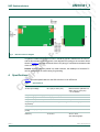
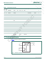
R
A
A
A
A
A
FT
FT
FT
FT
FT
D
R
R
A
A
FT
FT
FT
FT
A
A
R
R
D
D
D
D
R
R
A
FT
FT
FT
A
A
R
R
D
D
D
R
A
F
FT
FT
A
A
R
R
D
D
User manual
D
Rev. 00.01 — 28 April 2009
R
R
R
R
SSL2101/2102 12 W mains dimmable LED driver
D
D
D
D
D
UM10341_1
D
FT
FT
A
A
R
R
D
D
D
R
A
FT
D
R
A
Document information
Info
Content
Keywords
dimmable, SSL2101, SSL2102, SSL1523, driver, Mains supply, AC/DC
conversion, LED driver, User manual
Abstract
This document is a user manual for the SSL2101/SSL2102 mains
dimmable 12 W LED driver demo boards.
D
D
D
D
D
R
R
R
R
R
A
A
A
UM10341_1
A
A
FT
FT
FT
FT
FT
D
R
R
A
A
A
A
R
R
D
D
D
NXP Semiconductors
R
D
R
F
FT
A
A
D
R
A
A
R
FT
FT
First draft
D
<tbd>
FT
01
A
Description
FT
R
R
Date
A
D
D
Rev
D
R
FT
FT
A
A
R
R
D
D
D
Revision history
FT
FT
FT
FT
SSL2101/SSL2102 12 W LED driver
D
D
R
A
FT
D
R
A
Contact information
For more information, please visit: http://www.nxp.com
For sales office addresses, please send an email to: [email protected]
UM10431_1
User manual
© NXP B.V. 2009. All rights reserved.
Rev. 00.01 — 28 April 2009
2 of 24
D
D
D
D
D
R
R
R
R
R
A
A
A
UM10341_1
A
A
FT
FT
FT
FT
FT
D
R
R
A
A
A
A
R
R
D
D
D
NXP Semiconductors
D
R
R
A
FT
FT
FT
A
A
R
R
D
D
D
R
A
F
FT
FT
A
A
R
R
D
D
D
1. Introduction
FT
FT
FT
FT
SSL2101/SSL2102 12 W LED driver
D
FT
FT
A
A
R
R
D
The SSL2101/2102 12 W LED driver is a solution for a professional application with
multiple high power LEDs that requires galvanic isolation and a safe output voltage. It is
mains dimmable for both forward phase (TRIAC) dimmers, and reverse phase (Transistor)
dimmers. It can generate up to 16 W output power, which is equal to a 100 W
incandescent lamp (at 63 Lumen/W). Examples are shelf lighting, down lighting, LED
lighting for bathrooms etc.The design gives an example of how to make a drive that is
suitable for small form factor applications like retrofit lamps.
D
D
R
A
Variac isolation symbols
3. Connecting the board
The board can be optimized for a 230 V (AC) (50 Hz) or for a 120 V (AC) (60 Hz) mains
source. Besides the mains voltage optimization, the board is designed to work with
multiple high power LEDs with a total working voltage of between 9 V and 23 V. The
output current can be limited using trimmer R20. On request, a dedicated LED load can
be delivered that is to be connected to K3. Connector K2 can be used to attach other LED
loads. The output voltage is limited to 25 V. When attaching a LED load to an operational
board (hot plugging) an inrush peak current will occur due to discharge of capacitor C6.
After frequent discharges, the LEDs may deteriorate or become damaged.
Contact information
For more information, please visit: http://www.nxp.com
For sales office addresses, please send an email to: [email protected]
UM10431_1
User manual
© NXP B.V. 2009. All rights reserved.
Rev. 00.01 — 28 April 2009
3 of 24
A
Fig 1.
b. Not Isolated
R
a. Isolated
D
The board needs to be connected to mains voltage. Touching the reference board during
operation must be avoided at all times. An isolated housing is obligatory when used in
uncontrolled, non laboratory environments. Even though the secondary circuit with LED
connection has a galvanic isolation, this isolation is not according to any regulated norm.
Galvanic isolation of the mains phase using a variable transformer is always
recommended. These devices can be recognized by the symbols shown in Figure 1:
FT
2. Safety warning
D
D
D
D
D
R
R
R
R
R
A
A
A
UM10341_1
A
A
FT
FT
FT
FT
FT
D
R
R
A
A
A
A
R
R
D
D
D
NXP Semiconductors
FT
FT
FT
FT
SSL2101/SSL2102 12 W LED driver
D
R
R
A
FT
FT
FT
A
A
R
R
D
D
D
R
A
F
FT
FT
A
A
R
R
D
D
D
D
FT
FT
A
A
R
R
D
D
D
R
A
FT
D
R
A
Fig 2.
Board connection diagram
If a galvanic isolated transformer is used, it should be placed in between the AC source
and the dimmer/demo board. Connect a user defined LED (string) to the connector K2 as
shown in Figure 2. Note that the anode of the LED (string) is connected to the bottom side
of this connector.
Remark: When the board is placed in a metal enclosure, the middle pin of connector P1
can be connected to the metal casing for grounding.
4. Specifications
Table 1 gives the specifications for the SSL2101/2102 12 W LED driver
Table 1.
Specifications
Comment
AC line input voltage
85 V (AC) to 276 V (AC)
Board has been optimized for
230 V (AC) or 120 V (AC)
± 10 % variation
Output voltage (LED voltage)
9 V (DC) to 23 V (DC)
Output voltage protection
25 V (DC)
Output current (LED current)
400 mA to 800 mA
Output voltage /load current
dependency
<+-4 % / Volt in regulated range See attached graphs
Current ripple
+/-150 mA
at 500 mA
Maximum output power (LED
power)
17 W
At Vout + 21 V
Efficiency
70 %-78 %
At tamb= 25°C
Adjustable with trimmer
See attached graphs
UM10431_1
User manual
© NXP B.V. 2009. All rights reserved.
Rev. 00.01 — 28 April 2009
4 of 24
D
D
D
D
D
R
R
R
R
R
A
A
A
UM10341_1
A
A
FT
FT
FT
FT
FT
D
R
R
A
A
A
A
R
R
D
D
D
NXP Semiconductors
D
FT
FT
D
R
A
© NXP B.V. 2009. All rights reserved.
Rev. 00.01 — 28 April 2009
D
A
Demo board (top)
User manual
F
A
R
Between primary and
secondary circuit
5. Board photos
UM10431_1
A
R
D
LxWxH
+3/ −3 % in the range of 250 V
(AC) to 210 V (AC)
Fig 3.
R
R
D
+5/ −6 % in the range of
130 V (AC) to 110 V (AC)
FT
Input voltage /load current
FT
+/-4 KV
A
0 to 85 ° Celsius
Isolation voltage
A
Operating temperature
R
103mm x 50mm x 20mm
D
Board dimensions
FT
100% – 0%
A
Dimming range
at 15 W output power
at 15 W output power
at 11 W output power
D
R
R
60-75 kHz
FT
D
D
Switching frequency
dependency
FT
FT
230 V(AC)
0.99
0.94
0.90
A
A
A
Comment
Power Factor: 120 V(AC)
R
R
R
Specifications
D
D
D
Table 1.
FT
FT
FT
FT
SSL2101/SSL2102 12 W LED driver
5 of 24
D
D
D
D
D
R
R
R
R
R
A
A
A
UM10341_1
A
A
FT
FT
FT
FT
FT
D
R
R
A
A
A
A
R
R
D
D
D
NXP Semiconductors
FT
FT
FT
FT
SSL2101/SSL2102 12 W LED driver
D
R
R
A
FT
FT
FT
A
A
R
R
D
D
D
R
A
F
FT
FT
A
A
R
R
D
D
D
D
FT
FT
A
A
R
R
D
D
D
R
A
FT
D
R
A
Fig 4.
Demo board (bottom)
6. Dimmers
Several TRIAC based dimmers have been tested by NXP Semiconductors. As different
dimmers have different specifications, the dimming performance of the board may vary.
Table 2 shows the range of dimmers that have been tested with the board:
Table 2.
Dimmer selection
Manufacturer Type
Voltage V
(AC)
Power range
(W)
Load
Min. dimming
range
Opus
852.390
230
60-400
Ha/Inc
0.6%
Opus
852.392
230
20-500
Inc
0.05%
Bush-Jaeger
2250U
230
20-600
Ha/Inc
0.03%
Bush-Jaeger
2247U
230
20-500
Ha/Inc
0.07%
Bush-Jaeger
6519U
230
40-550
Ha/Inc
8.4%
Gira
1184
230
60-400
Inc
1%
Everflourish
EFO700D
230
50-300
Ha/Inc
0.2%
Drespa
0817
230
20-315
Ha/Inc
3.4%
Ehmann
39 Domus
230
20-500
Ha/Inc
1%
Drespa
815
230
20-500
Inc
1.1%
Lutron
TG-600PH-W
H
120
600
Inc
0 %(off)
Levitron
L12-6641-W
120
600
Inc
0 %(off)
Levitron
L02-700-W
120
600
Inc
0 %(off)
Levitron
6602-IW
120
600
Inc
0 %(off)
Levitron
6683-W
120
600
Inc
0 %(off)
UM10431_1
User manual
© NXP B.V. 2009. All rights reserved.
Rev. 00.01 — 28 April 2009
6 of 24
D
D
D
D
D
R
R
R
R
R
A
A
A
UM10341_1
A
A
FT
FT
FT
FT
FT
D
R
R
A
A
A
A
R
R
D
D
D
NXP Semiconductors
D
FT
R
Power range
(W)
Load
Min. dimming
range
Levitron
R12-6631-LW
120
600
Inc
0 %(off)
Cooper
6001
120
600
Inc
0 %(off)
Lutron
MIR-600THW- 120
WH
600
Ha/Inc
0.9 %
D
FT
FT
A
A
R
R
D
R
A
FT
D
R
A
The board can be equipped with either the SSL2101 or SSL2102, depending on the
operating conditions and output power. The SSL2102 has lower thermal resistance and is
thus more suitable for higher temperatures and higher loads. The IC has several internal
functions. It controls and drives the flyback converter part, and it ensures proper dimmer
operation. In the IC itself, there are several high voltage switches integrated. One of these
switches controls the flyback input power, and it is situated between the Drain pin and
Source pin. On closing, a current will start to run, which stores energy in the transformer
TX1. This current is interrupted when the duty factor has exceeded the level set by the
PWMLimit pin, with a maximum of 75 %, or when the voltage on the Source pin exceeds
0.5 V. At the next cycle, the energy stored in the transformer is discharged to D6 and the
output capacitors C5 and C6, and finally absorbed by the load. The converter frequency is
set with an internal oscillator, the timing of which is controlled by external RC components
on pins RC and RC2. The frequency can be modulated using the brightness pin to an
upper and lower value. The ratio between R15 and R16 sets the frequency variation.
© NXP B.V. 2009. All rights reserved.
Rev. 00.01 — 28 April 2009
D
D
7. Functional description
User manual
F
FT
FT
Voltage V
(AC)
A
A
A
R
R
D
D
D
Manufacturer Type
UM10431_1
R
A
FT
FT
A
A
R
R
R
Dimmer selection
D
D
D
Table 2.
FT
FT
FT
FT
SSL2101/SSL2102 12 W LED driver
7 of 24
D
D
D
D
D
R
R
R
R
R
A
A
A
UM10341_1
A
A
FT
FT
FT
FT
FT
D
R
R
A
A
A
A
R
R
D
D
D
NXP Semiconductors
FT
D
A
F
FT
FT
A
A
R
R
R
WBLEED
R
A
D
D
SBLEED
D
R
FT
FT
A
A
R
R
D
D
D
ISENSE
FT
FT
FT
FT
SSL2101/SSL2102 12 W LED driver
D
FT
1
FT
A
A
R
R
D
10
2
D
D
R
A
DRAIN
R
16
SUPPLY
D
A
VCC
FT
BLEEDER
3
VALLEY
11
GND
LOGIC
4, 5,13,
14, 15
AUX
100 mV
Stop
RC
8
OSCILLATOR
12
Low freq
SOURCE
Blank
THERMAL
SHUTDOWN
BRIGHTNESS
RC2
POWER - UP
RESET
6
7
PROTECTION
LOGIC
FRC
Overcurrent
PWMLIMIT
9
0.5 V
PWM
LIMIT
CIRCUIT
1.5 V
Short-winding protection
014aaa567
Fig 5.
Block diagram SSL2101
The two other switches are called the weak-bleeder (pin Wbleed), and the strong bleeder
(pin Sbleed). When the voltage on both these pins is below a certain value (typical 52 V)
the Sbleed switch closes, providing a current path that loads the dimmer during zero
voltage crossing. This resets the dimmer timer. When the voltage on both these pins is
above 52 V, and the voltage on the Isens pin is above 100 mV, the weak-bleeder switch
closes. Using Q3, this current is boosted and provides a current path that loads the
dimmer when the converter draws insufficient current to have the dimmer latching stable.
Whilst the strong bleeder is always enabled, the weak-bleeder will activate only when the
output power drops below 8 W. This happens when the LEDs are dimmed, or when the
maximum LED power is tuned below 8 W. See Figure 6 and Figure 7 that show bleeder
voltage versus time in dimmed and un-dimmed position (low voltage = active):
UM10431_1
User manual
© NXP B.V. 2009. All rights reserved.
Rev. 00.01 — 28 April 2009
8 of 24
D
D
D
D
D
R
R
R
R
R
A
A
A
UM10341_1
A
A
FT
FT
FT
FT
FT
D
R
R
A
A
A
A
R
R
D
D
D
NXP Semiconductors
FT
FT
FT
FT
SSL2101/SSL2102 12 W LED driver
D
R
R
A
FT
FT
FT
A
A
R
R
D
D
D
R
A
F
FT
FT
A
A
R
R
D
D
D
D
FT
FT
A
A
R
R
D
D
D
R
A
FT
D
R
A
Fig 6.
Dimmed bleeder operation
Fig 7.
Un-dimmed bleeder operation
This board is optimized to work with a power factor above 0.9. In order to achieve this, the
converter operates at constant ton mode. The output power of the converter is buffered by
capacitor C6. Due to this configuration, the circuit has a resistive input current behaviour
in un-dimmed operation (see Input in Figure 7). In dimmed operation however, not only
the dimmer latch and hold current must be maintained, but a damper must be added to
dampen the inrush current and to dissipate the electric power that was stored in the LC
filter within the dimmer. Though at low power ranges (<10 W) a serial resistor can be used
for this, at higher power ranges a single series resistor is not efficient because the
converter supply current will cause significant voltage drop and thus dissipation through
UM10431_1
User manual
© NXP B.V. 2009. All rights reserved.
Rev. 00.01 — 28 April 2009
9 of 24
D
D
D
D
D
R
R
R
R
R
A
A
A
UM10341_1
A
A
FT
FT
FT
FT
FT
D
R
R
A
A
A
A
R
R
D
D
D
NXP Semiconductors
FT
FT
FT
FT
SSL2101/SSL2102 12 W LED driver
D
R
R
A
FT
FT
FT
A
A
R
R
D
D
D
D
R
A
F
FT
FT
A
A
R
R
D
D
this resistor. On the demonstration board, a combination of serial resistance and a parallel
damper has been chosen to improve efficiency. The serial resistor is made up of F1, R1,
R2 and R12. The parallel damper is made of C2 and R3. See Figure 8.
D
FT
FT
A
A
R
R
D
D
D
The input circuit of the converter must be equipped with a filter that is partially capacitive.
The combination of C1, L1, L2, C3 and C4 makes a filter that blocks most of the
disturbance generated by the converter input current. A drawback of this filter is a
reduction of power factor, due to the capacitive load. A lower converter power in relation to
the capacitive value of this filter/buffer will cause a lower power factor. At the 230 V (AC)
design using 150 nF capacitors, a power factor of 0.9 is reached at 11 W output power.
R
A
8.1 Changing the output voltage and LED current
One of the major advantages of a flyback converter over other topologies, is that it is
suitable for driving other output voltages. Essentiality, changing the winding ratio whilst
maintaining the value of the primary inductance, will shift the output working voltage
accordingly. Part of the efficiency of the driver is linked to the output voltage. A lower
output voltage will increase the transformation ratio, and cause higher secondary losses.
In practice, a mains dimmable flyback converter will have an efficiency between 80 % for
high output voltages (like 60 V) down to 50 % for low output voltages (like 3 V). At low
voltages, synchronous rectification might become advisable to reduce losses. The NXP
TEA1791 can be applied for this purpose. For exact calculations of transformer properties
and peak current, we refer to application note AN10754_1, “How to design an LED driver
using the SSL2101”, and the excel spreadsheet that goes with it.
8.2 Changing the output ripple current
The output current ripple is mostly determined by the LED voltage, the LED dynamic
resistance and the output capacitor. Whilst the value of C6 has been chosen to optimize
capacitor size with light output. A ripple of ± 25 % will result in an expected deterioration of
light output <1 %.
UM10431_1
User manual
© NXP B.V. 2009. All rights reserved.
Rev. 00.01 — 28 April 2009
10 of 24
A
The following modifications can be done in order to meet different customer application
requirements:
R
8. Board optimization
D
The dimming range is detected by sensing the average rectified voltage. R4, R5 and R17
make a voltage divider, and C9 filters the resulting signal. The converter sets its duty
factor and converter frequency accordingly.
FT
The board is equipped with a feedback loop that limits the output current. This feedback
loop senses the LED current over sense resistor R18, and a current mirror is made of
Q1/Q2. Using R20, the current level can be set. The same feedback loop is also used for
overvoltage protection. If the LED voltage exceeds 23 V, a current through R19 and D9
will start running. The current through the opto coupler IC2 will pull down the PWM_Limit
and brightness pin. At a value below 400 mV, the on time is zero. The feedback loop has
proportional action only, and the gain is critical because of phase shift caused by the
converter and C6. The relation between PWM_Limit and output current is quadratic in
nature. The resulting output current spread will be acceptable for most LED applications.
D
D
D
D
D
R
R
R
R
R
A
A
A
UM10341_1
A
A
FT
FT
FT
FT
FT
D
R
R
A
A
A
A
R
R
D
D
D
NXP Semiconductors
D
R
R
A
FT
FT
FT
A
A
R
R
D
D
D
R
A
F
FT
FT
A
A
R
R
D
D
D
D
D
FT
FT
A
A
R
R
The size for the buffer capacitor can be estimated from the following equation
I
1
C 6 = ----- ⋅ ----------------------------------------ΔI 6 ⋅ f net ⋅ R dynamic
FT
FT
FT
FT
SSL2101/SSL2102 12 W LED driver
D
D
As example: For a ripple current of ± 5%, and a mains frequency of 50 Hz, and a dynamic
resistance of 0.6 Ω, C6 becomes 20/(300*0.6) = 111 mF. For a ripple current of 25 % and
a dynamic resistance of 6 Ω, 4/(300*6) = 2200 μF. Using a series of LEDs, the dynamic
resistance of each LED can be added to the total dynamic resistance.
R
A
• Transistor dimmers contain active circuitry that require a load charge during the time
that the dimmer is open. The dimensioning of the circuit generating the internal supply
voltage inside the dimmer is made critical in order to avoid excessive internal dimmer
losses. This means that the remaining voltage drop over the lamp must be low
enough to reach this charge. For dimmers like the Busch-Jaeger 6519U, the minimum
lamp load is specified at 40 W which is equivalent to a 1.3 kΩ resistor load at
230 V(AC). Such a load would result in highly inefficient operation at low output power
levels, since most energy is waisted in order to drive the dimmer, and not to produce
light.
On the demo board, the weak bleeder value R6/R7 is choosen is such way, that losses
are still acceptable (about 2 W to 3 W) and only occur in dimmed position. The voltage
drop with some transistor dimmers is however not sufficient to cause full dimming range
control (minimum 10 % instead of <1 %), because at the SSL2101 the dimming range is
sensed by taking the average rectified voltage as input. To compensate for the reduced
voltage difference, voltage detection can be made more sensitive by replacing R4 with a
Zener diode, like the BZV85-C200 for 230 V(AC), or the BZV85-C68 for 120 V (AC)
applications. Because of increased sensitivity, the dimming curve when using TRIAC
dimmers, will also be steeper and shifted.
8.4 Changing the load curve
The load curve can be divided into two regions: A part where the control loop limits the
duty cycle of the converter, and where the output current is regulated, and a part where
the duty factor feedback is not dominant anymore. This last part occurs at output voltages
below 13 V. In this area, constant output power becomes the dominant control
mechanism. Changing the winding ratio of the transformer to match the output load will
also change this load curve.
UM10431_1
User manual
© NXP B.V. 2009. All rights reserved.
Rev. 00.01 — 28 April 2009
11 of 24
A
dimmers, there will be a sudden voltage difference over the input leading to a steep
charge of the input capacitors. The resulting peak current will lead to higher damper
dissipation. Because this steep charge is missing, the input capacitors will have less
stress, and the input circuit is less prune to audible noise.
R
• The negative phase causes no inrush current when the dimmer triggers. At TRIAC
D
Reverse phase (transistor) dimmers differ in two ways that can be beneficial but can also
cause problems with dimming detection:
FT
8.3 Adapting to high power reverse phase (transistor) dimmers.
D
D
D
D
D
R
R
R
R
R
A
A
A
UM10341_1
A
A
FT
FT
FT
FT
FT
D
R
R
A
A
A
A
R
R
D
D
D
NXP Semiconductors
D
R
R
A
FT
FT
FT
A
A
R
R
D
D
D
R
A
FT
FT
A
A
R
R
D
D
It is possible to attach multiple converters to a single dimmer. At the use of TRIAC
dimmers the inrush current will rise, though not proportionally to the number of converters.
Transistor dimmers are more suitable for usage with multiple converters because the
dimming range will increase due to the added bleeder action, and there is no inrush
current.
F
FT
FT
A
A
R
R
D
D
D
8.5 Multiple driver support
FT
FT
FT
FT
SSL2101/SSL2102 12 W LED driver
D
D
R
A
FT
D
R
A
UM10431_1
User manual
© NXP B.V. 2009. All rights reserved.
Rev. 00.01 — 28 April 2009
12 of 24
D
D
D
D
D
R
R
R
R
R
A
A
A
UM10341_1
A
A
FT
FT
FT
FT
FT
D
R
R
A
A
A
A
R
R
D
D
D
NXP Semiconductors
D
R
R
A
FT
FT
FT
A
A
R
R
D
D
D
R
A
F
FT
FT
A
A
R
R
D
D
D
9. Board schematic
FT
FT
FT
FT
SSL2101/SSL2102 12 W LED driver
D
FT
FT
A
A
R
R
D
D
D
R
A
FT
D
R
A
Fig 8.
Board schematic diagram
UM10431_1
User manual
© NXP B.V. 2009. All rights reserved.
Rev. 00.01 — 28 April 2009
13 of 24
D
D
D
D
D
R
R
R
R
R
A
A
A
UM10341_1
A
A
FT
FT
FT
FT
FT
D
R
R
A
A
A
A
R
R
D
D
D
NXP Semiconductors
FT
F
A
Package
Manuf.
Amount
Conn 3pin 2u ang m
SL 5.08/3/90
Weidmuller 1
K1'
Conn 3pin 2u
f
BL 5.08/3
Weidmuller 1
3
K3
Conn 6pin 1u
f
BL3.36Z
Fischer
4
K2
Conn 2pin 2u ang m
SL 5.08/2/90
Weidmuller 1
5
K2'
Conn 2pin 2u
f
BL 5.08/2
Weidmuller 1
6
F1
Fusistor
6.8E
1W
10 %
Free
1
7
R1
Resistor
39 Ω
1W
5%
Free
1
8
R2
Resistor
39 Ω
1W
5%
Free
1
9
R3
Resistor
1 KΩ
2W
5%
Free
1
10
R4
Resistor
470 KΩ
0.25
1%
Free
1
11
R5
Resistor
470 KΩ
0.25
1%
Free
1
12
R6
Resistor
10 KΩ
1W
5%
200
Free
1
13
R7
Resistor
10 KΩ
1W
5%
200
Free
1
14
R8
Resistor
2.2 KΩ
1W
5%
200
Free
1
15
R9
Resistor
2.2KΩ2
1W
5%
200
Free
1
D
Volt
FT
Tol.
D
Pwr
FT
Type
R
A
FT
A
Resistor
0.4 Ω
1W
1%
Free
1
R11
Resistor
33 KΩ
0.25
5%
200
Free
1
18
R12
Resistor
15 Ω
1W
5%
200
Free
1
19
R13
Resistor
100 KΩ
0.1
1%
200
Free
1
20
R14
Resistor
22 KΩ
0.1
1%
Free
1
21
R15
Resistor
470K
0.1
1%
Free
1
22
R16
Resistor
4.7 KΩ
0.1
1%
Free
1
23
R17
Resistor
12 KΩ
0.1
1%
Free
1
24
R18
Resistor
0.3 Ω
1W
1%
Free
1
25
R19
Resistor
10 KΩ
0.1
5%
Free
1
26
R20
Resistor
50 KΩ
Lin
0.1
5%
Horizontal
27
R21
Resistor
22 KΩ
0.1
1%
Free
1
28
R22
Resistor
330 Ω
0.1
1%
Free
1
29
R23
Resistor
470 Ω
0.25
5%
Free
1
30
R24
Resistor
3.9 KΩ
0.1
5%
Free
1
31
R25
Resistor
470 KΩ
0.25
5%
Free
1
32
R26
Resistor
10 KΩ
0.1
5%
Free
1
33
C1
Capacitor
470 pF
Cer
10 %
1K
DEBB33A471KC1B
Murata
1
34
C2
Capacitor
150 nF
Poly
10 %
400
NRM-S154K400F
NIC
1
35
C3
Capacitor
150 nF
Poly
10 %
400
NRM-S154K400F
NIC
1
36
C4
Capacitor
150 nF
Poly
10 %
400
NRM-S154K400F
NIC
1
37
C5
Capacitor
4.7μF
Poly
10 %
63
B32560J475K
Epcos
1
UM10431_1
R
R10
17
Bourns
D
1
16
User manual
R
A
2
R
K1
D
D
1
Value
A
FT
FT
Part
R
A
A
Par Ref.
t
Des.
No.
D
R
R
Bill of materials 230 V (AC)
R
A
D
D
Table 3.
D
R
FT
FT
A
A
R
R
D
D
D
10. Bill of materials (BOM)
FT
FT
FT
FT
SSL2101/SSL2102 12 W LED driver
1
© NXP B.V. 2009. All rights reserved.
Rev. 00.01 — 28 April 2009
14 of 24
D
D
D
D
D
R
R
R
R
R
A
A
A
UM10341_1
A
A
FT
FT
FT
FT
FT
D
R
R
A
A
A
A
R
R
D
D
D
NXP Semiconductors
D
R
A
F
R
330 pF
Cer
41
C9
Capacitor
10 μF
105° 10 %
42
C10
Capacitor
2.2 nF
Cer
10 %
4K
43
C11
Capacitor
10 nF
Cer
10 %
25
44
L1
Inductor
680 μH
744776268
Wurth
1
45
L2
Inductor
330 μH
744776233
Wurth
1
46
L3
Inductor
100 μH
47
TX1
Transformer
N87/3F3
48
D1
Rect Bridge
2A
49
D2
TVS diode
600 W
50
D3
Diode
1A
800 V
51
D4
Zener
270 V
3W
52
D5
Diode
53
D6
54
5%
25
Free
1
Free
1
DECE33J222ZC4B
Murata
Free
1
1
74477120
Wurth
1
EFD25
750340505
Wurth
1
SO-4
DBLS205G
Taiwan
semi
1
P6KE400A
Fairchild
1
HER107
Taiwan
semi
1
BZT03-C220
Vishay
1
1A
800 V
HER107
Taiwan
semi
1
Diode
3A
100 V
SK310A
Taiwan
semi
1
D7
Diode
1A
800 V
HER107
Taiwan
semi
1
55
D8
Zener
30 V
5%
BZV55-C30
NXP
1
56
D9
Zener
20 V
5%
BZV55-C20
NXP
1
57
D10
Diode
75 V
1N4148
NXP
1
58
Q1
Transistor
NPN
BC847B
NXP
1
59
Q2
Transistor
NPN
BC847B
NXP
1
60
Q3
Transistor
PNP
ZTX758
Zetex
1
61
ISO2 Optocoupler
4N27
Vishay
1
62
U1
IC
5%
SSL2101
SSL2102
SO-1
6SO20 W
Y
SSL2101/
SSL2102
Tol.
Volt
Package
A
Capacitor
R
C8
1
D
40
1
Free
1
Bill of materials 120 V (AC)
Part Ref.
No. Des.
Part
Value
1
K1
Conn 3pin 2u
ang
2
K1'
3
K3
Pwr
Type
Manuf.
Amount
m
SL 5.08/3/90
Weidmuller
1
Conn 3pin 2u
f
BL 5.08/3
Weidmuller
1
Conn 6pin 1u
f
BL3.36Z
Fischer
1
UM10431_1
User manual
© NXP B.V. 2009. All rights reserved.
Rev. 00.01 — 28 April 2009
D
25
FT
25
105° 10 %
A
105° 10 %
4.7 μF
R
2200 μF
Capacitor
D
Capacitor
C7
FT
C6
39
FT
A
A
R
38
Table 4.
D
Vishay
Amount
FT
2222 021 16222
A
Manuf.
D
Type
FT
Package
A
Volt
R
R
R
Tol.
D
D
D
Pwr
FT
FT
FT
Value
A
A
A
Part
R
R
R
Bill of materials 230 V (AC)
Par Ref.
t
Des.
No.
D
D
D
Table 3.
FT
FT
FT
FT
SSL2101/SSL2102 12 W LED driver
15 of 24
D
D
D
D
D
R
R
R
R
R
A
A
A
UM10341_1
A
A
FT
FT
FT
FT
FT
D
R
R
A
A
A
A
R
R
D
D
D
NXP Semiconductors
D
R
R
Amount
Weidmuller
1
Conn 2pin 2u
f
BL 5.08/2
Weidmuller
1
F1
Fusistor
6.8E
1W
10 %
Free
1
7
R1
Resistor
27 Ω
1W
5%
Free
1
8
R2
Resistor
27 Ω
1W
5%
Free
1
9
R3
Resistor
2.7 KΩ
1W
5%
Free
1
10
R4
Resistor
470 KΩ
0.25
1%
Free
1
11
R5
Resistor
0Ω
0.25
5%
Free
1
12
R6
Resistor
2.7 KΩ
1W
5%
200
Free
1
13
R7
Resistor
2.7 KΩ
1W
5%
200
Free
1
14
R8
Resistor
1 KΩ
1W
5%
200
Free
1
15
R9
Resistor
1 KΩ
1W
5%
200
Free
1
16
R10
Resistor
0.4 Ω
1W
1%
Free
1
17
R11
Resistor
33 KΩ
0.25
5%
200
Free
1
18
R12
Resistor
10 Ω
1W
5%
200
Free
1
19
R13
Resistor
100 KΩ
0.1
1%
200
Free
1
D
R
FT
FT
A
A
R
D
D
SL 5.08/2/90
F
m
A
Manuf.
FT
Type
R
1%
Free
1
0.1
1%
Free
1
22
R16
Resistor
10 KΩ
0.1
1%
Free
1
23
R17
Resistor
12 KΩ
0.1
1%
Free
1
24
R18
Resistor
0.3 Ω
1W
1%
Free
1
25
R19
Resistor
10 KΩ
0.1
5%
Free
1
26
R20
Resistor
50 KΩ
Lin
0.1
5%
Horizontal
Bourns
1
27
R21
Resistor
22 KΩ
0.1
1%
Free
1
28
R22
Resistor
330 Ω
0.1
1%
Free
1
29
R23
Resistor
3.9 KΩ
0.25
5%
Free
1
30
R24
Resistor
3.9 KΩ
0.1
5%
Free
1
0.25
5%
Free
1
Free
1
31
R25
Resistor
100 KΩ
32
R26
Resistor
NP
33
C1
Capacitor
470 pF
Cer
10 %
1 KV
DEBB33A471KC1B Murata
1
34
C2
Capacitor
100 nF
Poly
10 %
400
NRM-S104K400F
NIC
1
35
C3
Capacitor
330 nF
Poly
10 %
400
NRM-S334K400F
NIC
1
36
C4
Capacitor
330 nF
Poly
10 %
400
NRM-S334K400F
NIC
1
37
C5
Capacitor
4.7 μF
Poly
10 %
63
B32560J475K
Epcos
1
38
C6
Capacitor
2200 μF
105°
10 %
25
2222 021 16222
Vishay
1
39
C7
Capacitor
4.7 μF
105°
10 %
25
40
C8
Capacitor
330 pF
Cer
5%
41
C9
Capacitor
10 μF
105°
10 %
25
42
C10
Capacitor
2.2 nF
Cer
10 %
4K
Free
1
Free
1
Free
1
UM10431_1
DECE33J222ZC4B Murata
A
0.1
470 KΩ
R
15 KΩ
Resistor
D
Resistor
R15
FT
R14
21
A
20
User manual
D
A
Package
FT
R
Volt
D
6
D
K2'
Tol.
FT
5
Pwr
A
Conn 2pin 2u
ang
R
K2
D
4
FT
FT
Value
A
A
A
Part
R
R
R
Bill of materials 120 V (AC)
Part Ref.
No. Des.
D
D
D
Table 4.
FT
FT
FT
FT
SSL2101/SSL2102 12 W LED driver
1
© NXP B.V. 2009. All rights reserved.
Rev. 00.01 — 28 April 2009
16 of 24
D
D
D
D
D
R
R
R
R
R
A
A
A
UM10341_1
A
A
FT
FT
FT
FT
FT
D
R
R
A
A
A
A
R
R
D
D
D
NXP Semiconductors
D
R
Volt
Package
Amount
43
C11
Capacitor
10 nF
Cer
10 %
25
Free
44
L1
Inductor
680 μH
744776268
Wurth
1
45
L2
Inductor
330 μH
744776233
Wurth
1
46
L3
Inductor
100 μH
74477120
Wurth
1
47
TX1
Transformer
N87/3F3
EFD25
750340505
Wurth
1
48
D1
Rect Bridge
2A
SO-4
DBLS205G
Taiwan semi 1
49
D2
TVS diode
600 W
P6KE270A
Fairchild
50
D3
Diode
1 A 800 V
HER107
Taiwan semi 1
51
D4
Zener
270 V
3W
BZT03-C220
Vishay
52
D5
Diode
1 A 800 V
HER107
Taiwan semi 1
53
D6
Diode
3 A 100 V
SK310A
Taiwan semi 1
54
D7
Diode
1 A 800 V
HER107
Taiwan semi 1
55
D8
Zener
30 V
5%
BZV55-C30
NXP
1
56
D9
Zener
20 V
5%
BZV55-C20
NXP
1
57
D10
Diode
75 V
1N4148
NXP
1
58
Q1
Transistor
NPN
BC847B
NXP
1
D
FT
FT
D
R
A
BC847B
NXP
1
PNP
MPSA92
NXP
1
61
ISO2
Optocoupler
4N27
Vishay
1
62
U1
IC
SSL2102
A
NPN
SSL2101/
R
Transistor
Transistor
SO-20
W
D
Q2
Q3
SO-16 Y
FT
1
60
SSL2102
A
1
59
SSL2101
A
R
R
D
1
1
11. Transformer specification
Figure 9 shows the transformer schematic:
1
9
N1
2
N3
6
4
N2
5
Fig 9.
Transformer schematic
UM10431_1
User manual
© NXP B.V. 2009. All rights reserved.
Rev. 00.01 — 28 April 2009
D
Tol.
F
Pwr
FT
Value
FT
Part
A
A
A
Part Ref.
No. Des.
5%
R
D
R
R
Manuf.
FT
D
D
Type
A
FT
FT
A
A
R
R
R
Bill of materials 120 V (AC)
D
D
D
Table 4.
FT
FT
FT
FT
SSL2101/SSL2102 12 W LED driver
17 of 24
D
D
D
D
D
R
R
R
R
R
A
A
A
UM10341_1
A
A
FT
FT
FT
FT
FT
D
R
R
A
A
A
A
R
R
D
D
D
NXP Semiconductors
FT
N1
1X0.315
8
ISO
0.2
1
21
9
6
1
42
5
4
1
42
A
7
2
R
0.2
43
D
1X0.2
ISO
1
11.2 Electrical characteristics
Table 6.
Inductance
Section
Inductance
N1
910 μH ± 5 %, at 2.3 A
N2
70 μH
N3
270 μH
• Nominal frequency = 100 kHz
• Vbreakdown N1...N2 = 4 KV
11.3 Core and bobbin
• Core: EFD25, 3F3/N87, airgap center 1100 μM
• Bobbin: CSH-EFD25-1S-10P
UM10431_1
User manual
D
N2
6
F
5
A
0.2
1
FT
ISO
FT
4
A
40X0.071
A
N3
R
3
R
0.2
End
D
1X0.315
ISO
FT
Pin
A
Turns
R
N1
2
D
D
Layers
Begin
1
FT
FT
Wire
R
A
A
Section
D
R
R
No.
Winding specification
R
A
D
D
Table 5.
D
R
FT
FT
A
A
R
R
D
D
D
11.1 Winding specification
FT
FT
FT
FT
SSL2101/SSL2102 12 W LED driver
© NXP B.V. 2009. All rights reserved.
Rev. 00.01 — 28 April 2009
18 of 24
D
D
D
D
D
R
R
R
R
R
A
A
A
UM10341_1
A
A
FT
FT
FT
FT
FT
D
R
R
A
A
A
A
R
R
D
D
D
NXP Semiconductors
D
R
R
A
FT
FT
FT
A
A
R
R
D
D
D
R
A
F
FT
FT
A
A
R
R
D
D
D
11.4 Physical dimensions
FT
FT
FT
FT
SSL2101/SSL2102 12 W LED driver
D
FT
FT
A
A
R
R
D
D
D
R
A
FT
D
R
A
Fig 10. Transformer dimensions
12. Appendix A - Load curves
120 V (AC) load curves
1.200
500 mA
800 mA
650 mA
1.100
1.000
Iout
0.900
0.800
0.700
0.600
0.500
0.400
6
8
10
12 Uload 14
16
18
20
22
Fig 11. 120 V (AC) load curve
UM10431_1
User manual
© NXP B.V. 2009. All rights reserved.
Rev. 00.01 — 28 April 2009
19 of 24
D
D
D
D
D
R
R
R
R
R
A
A
A
UM10341_1
A
A
FT
FT
FT
FT
FT
D
R
R
A
A
A
A
R
R
D
D
D
NXP Semiconductors
D
R
R
A
FT
FT
FT
A
A
R
R
D
D
D
R
A
F
FT
FT
A
A
R
R
D
D
D
D
D
R
A
1 .200
D
FT
500 mA
800 mA
700 mA
FT
1 .300
FT
A
A
R
R
D
230 V (AC) load curves
FT
FT
FT
FT
SSL2101/SSL2102 12 W LED driver
D
R
1 .100
A
1 .000
Iout
0 .900
0 .800
0 .700
0 .600
0 .500
0 .400
9
11
13
15
Uload
17
19
21
23
Fig 12. 230 V (AC) load curve
13. Appendix B - Efficiency curves
500 mA
800 mA
650 mA
120 V (AC) efficiency curves
80.0 %
75.0 %
n
70.0 %
65.0 %
60.0 %
55.0 %
6
8
10
12
Uload 14
16
18
20
22
Fig 13. 120 V (AC) efficiency curve
UM10431_1
User manual
© NXP B.V. 2009. All rights reserved.
Rev. 00.01 — 28 April 2009
20 of 24
D
D
D
D
D
R
R
R
R
R
A
A
A
UM10341_1
A
A
FT
FT
FT
FT
FT
D
R
R
A
A
A
A
R
R
D
D
D
NXP Semiconductors
D
R
R
A
FT
FT
FT
A
A
R
R
D
D
D
R
A
F
FT
FT
A
A
R
R
D
D
D
D
FT
D
D
R
A
FT
500 mA
800 mA
700 mA
FT
A
A
R
R
D
230 V (AC) efficiency curves
80 .0%
FT
FT
FT
FT
SSL2101/SSL2102 12 W LED driver
D
R
75 .0%
A
n
70 .0%
65 .0%
60 .0%
55 .0%
9
11
13
15
17
Uload
19
21
23
Fig 14. 230 V (AC) effeciency curve
14. Appendix C - Input voltage dependency
120 V (AC) input voltage dependency
230 V (AC) input voltage dependency
0.74
0.67
0.66
0.73
0.65
0.72
0.64
0.63
0.71
Iout (A)
Iout (A)
0.62
0.61
0.7
0.6
0.69
0.59
0.68
0.58
0.57
0.67
0.56
0.66
0.55
0.54
0.65
0.53
0.52
100
0.64
105
110
115
120
125
130
130
135
200
Vin (V)
205
210
215
220
225
230
235
240
245
250
Vin (V)
Fig 15. Input voltage/output current dependency
UM10431_1
User manual
© NXP B.V. 2009. All rights reserved.
Rev. 00.01 — 28 April 2009
21 of 24
D
D
D
D
D
R
R
R
R
R
A
A
A
UM10341_1
A
A
FT
FT
FT
FT
FT
D
R
R
A
A
A
A
R
R
D
D
D
NXP Semiconductors
FT
D
R
2
0
0
3
13.2
9
4
0
0
5
3.8
2.1
6
0
0.1
7
1.2
1.9
8
0.1
0.1
9
3.2
2
0
0.1
13
2.5
1.3
14
0
0.1
15
1.8
1.2
16
0
0.1
17
2.1
0.5
18
0
0
19
2.9
0.1
20
0
0
THD
15.94
10.80
PF
0.94
0.98
A
12
R
0
D
0.1
0.5
FT
0
11
A
10
[1]
AN10754_1 — How to design an LED driver using the SSL2101
[2]
SSL2101 — Datasheet
[3]
SMPS — IC for dimmable LED lighting
© NXP B.V. 2009. All rights reserved.
Rev. 00.01 — 28 April 2009
D
100
R
100
D
1
FT
120 V (AC) 60Hz Amplitude (%)
FT
A
A
R
230 V (AC) 50 Hz Amplitude (%)
16. References
User manual
F
D
D
Harmonic
UM10431_1
A
FT
FT
A
A
R
R
R
Mains conducted harmonic values
R
A
D
D
Table 7.
D
R
FT
FT
A
A
R
R
D
D
D
15. Appendix D - Mains conducted harmonics
FT
FT
FT
FT
SSL2101/SSL2102 12 W LED driver
22 of 24
D
D
D
D
D
R
R
R
R
R
A
A
A
UM10341_1
A
A
FT
FT
FT
FT
FT
D
R
R
A
A
A
A
R
R
D
D
D
NXP Semiconductors
D
A
FT
R
F
D
FT
FT
A
A
R
damage. NXP Semiconductors accepts no liability for inclusion and/or use of
NXP Semiconductors products in such equipment or applications and
therefore such inclusion and/or use is at the customer’s own risk.
R
D
R
A
17.4 Patents
Right to make changes — NXP Semiconductors reserves the right to make
changes to information published in this document, including without
limitation specifications and product descriptions, at any time and without
notice. This document supersedes and replaces all information supplied prior
to the publication hereof.
Notice is herewith given that the subject device uses one or more of the
following patents and that each of these patents may have corresponding
patents in other jurisdictions.
Suitability for use — NXP Semiconductors products are not designed,
authorized or warranted to be suitable for use in medical, military, aircraft,
space or life support equipment, nor in applications where failure or
malfunction of an NXP Semiconductors product can reasonably be expected
to result in personal injury, death or severe property or environmental
17.5 Trademarks
<Patent ID> — owned by <Company name>
Notice: All referenced brands, product names, service names and trademarks
are the property of their respective owners.
<Name> — is a trademark of NXP B.V.
UM10431_1
© NXP B.V. 2009. All rights reserved.
Rev. 00.01 — 28 April 2009
23 of 24
A
<License statement text> (replace by text inset t001lic<1nn>)
R
Purchase of NXP <xxx> components
D
General — Information in this document is believed to be accurate and
reliable. However, NXP Semiconductors does not give any representations or
warranties, expressed or implied, as to the accuracy or completeness of such
information and shall have no liability for the consequences of use of such
information.
FT
Applications — Applications that are described herein for any of these
products are for illustrative purposes only. NXP Semiconductors makes no
representation or warranty that such applications will be suitable for the
specified use without further testing or modification.
17.3 Licenses
17.2 Disclaimers
D
D
Draft — The document is a draft version only. The content is still under
internal review and subject to formal approval, which may result in
modifications or additions. NXP Semiconductors does not give any
representations or warranties as to the accuracy or completeness of
information included herein and shall have no liability for the consequences of
use of such information.
User manual
A
FT
FT
A
A
R
R
D
D
D
17.1 Definitions
R
R
FT
FT
A
A
R
R
D
D
D
17. Legal information
FT
FT
FT
FT
SSL2101/SSL2102 12 W LED driver
D
D
D
D
D
R
R
R
R
R
A
A
A
UM10341_1
A
A
FT
FT
FT
FT
FT
D
R
R
A
A
A
A
R
R
D
D
D
NXP Semiconductors
FT
R
F
FT
FT
A
A
A
D
FT
FT
A
A
R
R
D
D
D
R
A
FT
D
R
A
8.4
8.5
9
10
11
11.1
11.2
11.3
11.4
12
13
14
15
16
17
17.1
17.2
17.3
17.4
17.5
18
D
R
R
8.2
8.3
Introduction . . . . . . . . . . . . . . . . . . . . . . . . . . . . 3
Safety warning . . . . . . . . . . . . . . . . . . . . . . . . . . 3
Connecting the board . . . . . . . . . . . . . . . . . . . . 3
Specifications. . . . . . . . . . . . . . . . . . . . . . . . . . . 4
Board photos . . . . . . . . . . . . . . . . . . . . . . . . . . . 5
Dimmers . . . . . . . . . . . . . . . . . . . . . . . . . . . . . . . 6
Functional description . . . . . . . . . . . . . . . . . . . 7
Board optimization . . . . . . . . . . . . . . . . . . . . . 10
Changing the output voltage and LED
current . . . . . . . . . . . . . . . . . . . . . . . . . . . . . . 10
Changing the output ripple current . . . . . . . . . 10
Adapting to high power reverse phase
(transistor) dimmers.. . . . . . . . . . . . . . . . . . . . 11
Changing the load curve. . . . . . . . . . . . . . . . . 11
Multiple driver support . . . . . . . . . . . . . . . . . . 12
Board schematic . . . . . . . . . . . . . . . . . . . . . . . 13
Bill of materials (BOM) . . . . . . . . . . . . . . . . . . 14
Transformer specification . . . . . . . . . . . . . . . . 17
Winding specification . . . . . . . . . . . . . . . . . . . 18
Electrical characteristics . . . . . . . . . . . . . . . . . 18
Core and bobbin . . . . . . . . . . . . . . . . . . . . . . . 18
Physical dimensions . . . . . . . . . . . . . . . . . . . . 19
Appendix A - Load curves. . . . . . . . . . . . . . . . 19
Appendix B - Efficiency curves . . . . . . . . . . . 20
Appendix C - Input voltage dependency . . . . 21
Appendix D - Mains conducted harmonics . . 22
References . . . . . . . . . . . . . . . . . . . . . . . . . . . . 22
Legal information. . . . . . . . . . . . . . . . . . . . . . . 23
Definitions . . . . . . . . . . . . . . . . . . . . . . . . . . . . 23
Disclaimers . . . . . . . . . . . . . . . . . . . . . . . . . . . 23
Licenses . . . . . . . . . . . . . . . . . . . . . . . . . . . . . 23
Patents . . . . . . . . . . . . . . . . . . . . . . . . . . . . . . 23
Trademarks. . . . . . . . . . . . . . . . . . . . . . . . . . . 23
Contents . . . . . . . . . . . . . . . . . . . . . . . . . . . . . . 24
R
A
D
D
1
2
3
4
5
6
7
8
8.1
D
R
FT
FT
A
A
R
R
D
D
D
18. Contents
FT
FT
FT
FT
SSL2101/SSL2102 12 W LED driver
Please be aware that important notices concerning this document and the product(s)
described herein, have been included in section ‘Legal information’.
© NXP B.V. 2009.
All rights reserved.
For more information, please visit: http://www.nxp.com
For sales office addresses, please send an email to: [email protected]
Date of release: 28 April 2009
Document identifier: UM10431_1