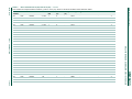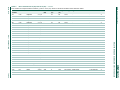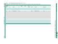
1
UM10433
SSL2103 dimmable isolated LED driver demo board
Rev. 1 — 9 December 2010
User manual
Document information
Info
Content
Keywords
SSL2103, LED driver, mains dimmable, constant current, driver, mains
supply, AC/DC conversion, user manual.
Abstract
This is a user manual for the SSL2103 mains dimmable 22 W LED.
UM10433
NXP Semiconductors
SSL2103 dimmable isolated LED driver demo board
Revision history
Rev
Date
Description
v.1
20101209
First issue
UM10433
User manual
All information provided in this document is subject to legal disclaimers.
Rev. 1 — 9 December 2010
© NXP B.V. 2010. All rights reserved.
2 of 29
UM10433
NXP Semiconductors
SSL2103 dimmable isolated LED driver demo board
1. Introduction
The SSL2103 LED driver board is an isolated flyback converter featuring the SSL2103
controller. It is designed for applications with multiple high power LEDs that require high
efficiency, galvanic isolation and a safe output voltage. It is mains dimmable for both
forward phase (triac) dimmers, and reverse phase (transistor) dimmers. The design is
aimed to demonstrate high performance and efficiency. It operates at 70 kHz and
produces a regulated output current of up to 800 mA to drive from 6 LEDs to 18 LEDs
using a 120 V (AC) or 220 V (AC) input. It can achieve an efficiency of up to 85 % with the
help of an external MOSFET transistor. Isolation voltage is 2500 V.
2. Safety warning
WARNING
Lethal voltage and fire ignition hazard
The non-insulated high voltages that are present when operating this product, constitute a
risk of electric shock, personal injury, death and/or ignition of fire.
This product is intended for evaluation purposes only. It shall be operated in a designated test
area by personnel qualified according to local requirements and labor laws to work with
non-insulated mains voltages and high-voltage circuits. This product shall never be operated
unattended.
The board is to be connected to a mains supply so touching the reference board during
operation must be avoided at all times. An isolated housing is obligatory when used in
uncontrolled, non laboratory environments. Even though the secondary circuit with LED
connections has galvanic isolation, this isolation is not according to any regulated norm.
Galvanic isolation of the mains phase using a variable transformer is always
recommended. These devices can be recognized by the symbols shown in Figure 1.
019aaa690
a. Isolated
Fig 1.
UM10433
User manual
019aaa691
b. Not Isolated
Variac isolation symbols
All information provided in this document is subject to legal disclaimers.
Rev. 1 — 9 December 2010
© NXP B.V. 2010. All rights reserved.
3 of 29
UM10433
NXP Semiconductors
SSL2103 dimmable isolated LED driver demo board
3. Connecting the board
Remark: All components referred to in the text can be located on Figure 7 “Board
schematic diagram (part 1)” or Figure 8 “Board schematic diagram (part 2)” and
connectors can be found on Figure 2 “Board connection diagram”.
The board is optimized for either a 230 V (50 Hz) or a 120 V (60 Hz) mains supply. In
addition to optimizing the mains voltage, the board is designed to work with multiple
high-power LEDs with a total working voltage of between 20 V and 63 V. The output
current can be limited using trimmer R68. It is possible to request the delivery of a
dedicated LED load that is to be connected to K3. Connector K2 can be used to attach
other LED loads. The output voltage is limited to 65 V. It is recommended to connect the
LED load to the driver board, before powering up the driver, to avoid potential damage to
LEDs due to inrush current as a result of the hot-plugging.
K1
K2
L
−
LED−
+
LED+
N
−
LED−
K3
LED+
+
019aaa820
Fig 2.
Board connection diagram
If a galvanically isolated transformer is used, it should be placed between the AC source
and the dimmer/demo board. Connect a user defined LED (string) to connector K2 as
shown in Figure 2. Note that the anode of the LED (string) is connected to the bottom side
of this connector.
Remark: When the board is placed in a metal enclosure, the middle pin of connector K1
should be connected to the metal casing for grounding.
UM10433
User manual
All information provided in this document is subject to legal disclaimers.
Rev. 1 — 9 December 2010
© NXP B.V. 2010. All rights reserved.
4 of 29
UM10433
NXP Semiconductors
SSL2103 dimmable isolated LED driver demo board
4. Specifications
Table 1 provides the specifications for the SSL2103 22 W LED driver
Table 1.
Specifications
Parameter
Value
Comment
AC line input voltage
85 V (AC) to 276 V (AC)
board has been optimized for
230 V (AC) or 120 V (AC)
± 10 % variation
Output voltage (LED voltage)
20 V (DC) to 63 V (DC)
minimum load = 6 LEDs
maximum load = 18 LEDs
Output voltage protection
65 V (DC)
Output power (LED power)
22 W nominal
Efficiency
> 80 %
at Tamb = 25 °C,
nominal input voltage,
nominal output current,
maximum load (18 LEDs),
See Figure 13 and Figure 14
Power Factor
> 0.9
nominal input voltage,
nominal output current,
maximum load (18 LEDs),
Output current (LED current)
350 mA nominal
adjustable with trimmer to
800 mA at minimum load
(6 LEDs)
Load current accuracy/output
voltage dependency
<5%
nominal output current,
See Figure 11 and Figure 12
Load current accuracy/input
voltage dependency
<5%
nominal output current,
See Figure 15 and Figure 16
Output current ripple
60 mA
nominal output current,
maximum load (18 LEDs), See
Figure 19
Switching frequency
50 kHz to 90 kHz
-
See Figure 17 and Figure 18
UM10433
User manual
Dimming range
100 % to 0 %
for triac dimmer
Board dimensions
117 mm × 50 mm × 30 mm
L×W×H
Operating temperature
0 °C to 85 °C
-
Isolation voltage
2.5 kV
between primary and secondary
circuit
All information provided in this document is subject to legal disclaimers.
Rev. 1 — 9 December 2010
© NXP B.V. 2010. All rights reserved.
5 of 29
UM10433
NXP Semiconductors
SSL2103 dimmable isolated LED driver demo board
5. Board photographs
019aab014
Fig 3.
Demo board (top)
019aab013
Fig 4.
Demo board (bottom)
UM10433
User manual
All information provided in this document is subject to legal disclaimers.
Rev. 1 — 9 December 2010
© NXP B.V. 2010. All rights reserved.
6 of 29
UM10433
NXP Semiconductors
SSL2103 dimmable isolated LED driver demo board
6. Dimmers
Numerous dimmers have been tested by NXP Semiconductors. The dimming
performance of the board may vary as different dimmers have different specifications.
Table 2 and Table 3 show the range of dimmers that have been tested and found to be
compatible with the board.
Table 2.
Manufacturer
Type
Voltage V (AC)
Power range (W)
Load
BERKER
2819
230
60 to 400
incandescent
BERKER
2873
230
20 to 500
halogen/incandescent
Bush-Jaeger
2250U
230
60 to 600
halogen/incandescent
Bush-Jaeger
2200U
230
60 to 400
incandescent
LICHTREGLER
T10
230
60 to 300
incandescent
Gira
0300
230
60 to 400
incandescent
Gira
1184
230
60 to 400
incandescent
Lutron
S-600PH-WH
120
600
halogen/incandescent
Lutron
MIR-600
120
600
halogen/incandescent
Levitron
6602-IW
120
600
incandescent
Table 3.
UM10433
User manual
Triac dimmer selection
Transistor dimmer selection
Manufacturer
Type
Voltage V (AC)
Power range (W)
Load
JUNG
243 EX
230
20 to 360
halogen/incandescent
JUNG
225 TDE
230
20 to 525
halogen/incandescent
BERKER
2874
230
20 to 525
halogen/incandescent
BERKER
286710
230
20 to 360
halogen/incandescent
Bush-Jaeger
6513U
230
40 to 420
halogen/incandescent
Gira
0307
230
20 to 525
halogen/incandescent
PEHA
433 HAB
230
20 to 315
halogen/incandescent
All information provided in this document is subject to legal disclaimers.
Rev. 1 — 9 December 2010
© NXP B.V. 2010. All rights reserved.
7 of 29
UM10433
NXP Semiconductors
SSL2103 dimmable isolated LED driver demo board
7. Functional description
Remark: All components referred to in the text can be located in Figure 7 “Board
schematic diagram (part 1)” or Figure 8 “Board schematic diagram (part 2)”.
The IC SSL2103 is the latest extension to the SSL2101/SSL2102 platform and gives
designers the flexibility of any power level by controlling external switches. In this
application, it controls the flyback converter part and ensures proper dimmer operation.
One of these switches controls the flyback input power and stores energy in the
transformer TR1. The switch is opened when the duty factor has exceeded the level set
by the PWMLIMIT pin, with a maximum of 75 %, or when the voltage on the SOURCE pin
exceeds 0.5 V. The energy stored in the transformer is then discharged to D10 and the
output capacitors, and finally absorbed by the load.
When dimmers are used, the circuit detects the rectified voltage change and reduces the
duty cycle and oscillator frequency to reduce the output current.
The circuit has a bleeding circuit that drives two external current sinks called bleeders.
These are the weak bleeder (pin WB_DRV) and the strong bleeder (pin SB_DRV).
When the voltage on both of these pins is below a certain value (typically 52 V) the strong
bleeder switch (T4) closes, providing a current path that loads the dimmer during zero
voltage crossing. This results in the dimmer timer being reset.
When the voltage on either of these pins is above 52 V, and the voltage on the ISENSE
pin is above −100 mV, the weak bleeder switch (T3) closes. This provides a current path
that loads the dimmer while the converter draws insufficient current to stabilize the dimmer
latching.
The strong bleeder will always switch but the weak bleeder will not activate until the output
power drops below 8 W. This happens when the LEDs are dimmed or when the maximum
LED power is tuned to below 8 W. It allows the system to operate with the majority of field
installed dimmers. See Figure 5 and Figure 6 that show bleeder drive outputs compared
with time, for dimmed and undimmed operations.
UM10433
User manual
All information provided in this document is subject to legal disclaimers.
Rev. 1 — 9 December 2010
© NXP B.V. 2010. All rights reserved.
8 of 29
UM10433
NXP Semiconductors
SSL2103 dimmable isolated LED driver demo board
WB_DRV
SB_DRV
Vinput
Iinput
019aab016
Fig 5.
Dimmed bleeder operation
UM10433
User manual
All information provided in this document is subject to legal disclaimers.
Rev. 1 — 9 December 2010
© NXP B.V. 2010. All rights reserved.
9 of 29
UM10433
NXP Semiconductors
SSL2103 dimmable isolated LED driver demo board
WB_DRV
SB_DRV
Vinput
Iinput
019aab015
Fig 6.
Undimmed bleeder operation
7.1 Bleeder settings
The demo board allows the users to disable the bleeders or choose between two
configurations of load. This ensures good operation of the dimmer with the converter or a
reduction of power losses in the bleeders.
• Weak bleeder - jumper (J1-J3) selects a current of 10 mA or 20 mA
• Strong bleeder - jumper (J2-J4) selects a current of 25 mA or 60 mA
7.2 Power factor
This board is optimized to work with a power factor above 0.9. In order to achieve this, the
converter operates at constant ton mode. The output power of the converter is buffered by
capacitors C21, C22, C23 and C34. Due to this configuration, the circuit has a resistive
input current behavior during undimmed operation (see Figure 6). During dimmed
operation however, not only the dimmer latch and hold current must be maintained, but a
damper must be added to dampen the inrush current and to dissipate the electrical power
stored in the LC filter within the dimmer. An active damping solution has been chosen for
the demo board to improve efficiency (see Section 7.5).
7.3 Dimming detection
The dimming reference voltage is derived from a non-buffered rectified mains voltage.
The dimming range is detected by sensing the average rectified voltage by a resistive
divider. The converter duty factor and frequency is set by the voltage on the
UM10433
User manual
All information provided in this document is subject to legal disclaimers.
Rev. 1 — 9 December 2010
© NXP B.V. 2010. All rights reserved.
10 of 29
UM10433
NXP Semiconductors
SSL2103 dimmable isolated LED driver demo board
BRIGHTNESS and PWMLIMIT pins (see Figure 7 and Figure 8). The peak current
through the inductor is reduced by balancing the voltage levels at these two inputs, before
the frequency of the converter falls. This eliminates audible noise from the transformer.
7.4 Output voltage and output current
Voltage and current regulation is achieved by utilizing two operational amplifiers. Both
amplifier outputs are in an or-configuration, to drive the optocoupler U2. This is done via
diodes D12 and D13 and the amplifier with the lowest output is dominant.
U3B is used for voltage control. The power supply output is sensed through resistive
divider R73 and R74 and presented to the inverting input of the operational amplifier. The
resistors are selected to provide 2.5 V to pin 5 when the output is at the desired maximum
voltage (approximately 62 V in this case). Frequency compensation is provided by R/C
network R71 and C28.
Current is controlled by sensing the output current through R61 and presenting the sense
signal to U3A where it is compared to a trimmed down value from VC1. The output
overcurrent threshold level is set by adjusting R68 so that the resultant voltage level
presented to pin 3 of U3, with no output load, equals the voltage drop that appears across
R61 at the maximum desired current. In this design, the nominal current is set at 350 mA
which requires 105 mV of bias at pin 3 under no output load. Frequency compensation
(bandwidth) of the current amplifier is set by R66 and C26.
7.5 Active damping - inrush current
A damper is required to limit inrush current. Inrush current occurs when the input
capacitors encounter fast voltage changes as in the following situations.
• when the board is hot-plugged into an AC input source.
• when the board is fed from a leading edge phase cut dimmer.
There are many ways to perform damping. A single resistor is the cheapest solution but
could lead to thermal issues and low efficiency. The damper resistor plays a major factor
in the power losses of the system. At low power ratings (< 10 W), a serial resistor is
suitable due to acceptable losses. At higher power, an active circuit becomes the
preferred solution to achieve high efficiency.
The solution applied here utilizes an active damper using a MOSFET transistor (T2). T2 is
used to bypass damping resistors R9 and R10 following inrush current. The MOSFET
transistor will be ON as long as the current in the circuit is small enough to keep the
bipolar transistor T1 from pulling down the gate of MOSFET T2.
UM10433
User manual
All information provided in this document is subject to legal disclaimers.
Rev. 1 — 9 December 2010
© NXP B.V. 2010. All rights reserved.
11 of 29
UM10433
NXP Semiconductors
SSL2103 dimmable isolated LED driver demo board
8. Board optimization
The following modifications must be carried out in order to meet different customer
application requirements.
8.1 Changing the output voltage and LED current
Compared to other topologies, a flyback converter has the major advantage that it is
suitable for driving a broader range of output voltages. Essentially, changing the turns
ratio while maintaining the value of the primary inductance, will shift the output working
voltage accordingly. The efficiency of the driver is linked to the output voltage. A lower
output voltage increases the transformation ratio and causes higher secondary losses. In
practice, a mains dimmable flyback converter has an efficiency of between 80 % for high
output voltages (such as 60 V) down to 50 % for low output voltages (such as 3 V).
Synchronous rectification might become advisable to reduce losses at low voltages. The
NXP TEA1791 can be used for this purpose. For exact calculations of transformer
properties and peak current, refer to application note AN10754 and the calculation tool
that is provided with it.
8.2 Changing the output ripple current
The LED voltage, the LED dynamic resistance and the output capacitor determine the
output current ripple. The value of Cout (21-22-23-34) has been chosen to optimize
capacitor size with light output. A ripple of ± 25 % results in an expected deterioration of
light output < 1 %.
The size for the buffer capacitor can be estimated from the following equation:
I LED
1
C out = ----------- × -------------------------------------------ΔI
6 × f net × R dynamic
(1)
Example:
For a ripple current of ± 5 % with a mains frequency of 50 Hz and a dynamic resistance of
0.6 Ω, C6 is 20 ÷ (300 × 0.6) = 111 μF. For a ripple current of 25 % and a dynamic
resistance of 6 Ω, 4 ÷ (300 × 6) = 2200 μF. Using a series of LEDs, the dynamic resistance
of each LED can be added to the total dynamic resistance.
8.3 Improving the power factor
The power factor can be increased by reducing the primary capacitance to an absolute
minimum to filter the converter. The current then follows the input voltage. This
modification has the following consequences:
• it is necessary to greatly increase the output capacitance to minimize the output
current ripple
• because the voltage ripple on the primary capacitors is larger, the peak current
through the inductor must increase to have the same output power. This results in
higher switching losses that can cause thermal issues. A transformer that can handle
the higher current is also required
• dimmer support is improved because the current follows the input voltage. However,
for some dimmer duty factors additional current bleeding is still necessary
UM10433
User manual
All information provided in this document is subject to legal disclaimers.
Rev. 1 — 9 December 2010
© NXP B.V. 2010. All rights reserved.
12 of 29
UM10433
NXP Semiconductors
SSL2103 dimmable isolated LED driver demo board
8.4 Adapting to high power reverse phase (transistor) dimmers.
Reverse phase (transistor) dimmers differ in two ways that can be beneficial but can also
cause problems with dimming detection:
• The negative phase-cut (trailing edge) causes no inrush current when the dimmer
triggers. Triac dimmers have a sudden voltage difference over the input leading to a
steep charge of the input capacitors. The resulting peak current leads to higher
damper dissipation. Because this steep charge is missing, the input capacitors have
less stress, and the input circuit is less prone to audible noise.
• Transistor dimmers contain active circuitry that requires a load charge during the time
that the dimmer is active. The dimensioning of the circuit generating the internal
supply voltage inside the dimmer is made critical in order to avoid excessive internal
dimmer losses. This results in the remaining voltage drop over the lamp being low
enough to reach the load charge. For dimmers such as the Busch-Jaeger 6519U, the
minimum lamp load is specified at 40 W which is equivalent to a 1.3 kΩ resistor load
at 230 V (AC). Such a load results in highly inefficient operation at low output power
levels, since most energy is wasted driving the dimmer instead of producing light.
To minimize losses, the weak bleeder on the demo board is set to a maximum current of
either 10 mA or 20 mA by using a jumper. The weak bleeder normally only switches on
during dimmed operation. The voltage drop with some transistor dimmers is, however, not
sufficient to cause full dimming range control (minimum 10 % instead of < 1 %). This is
because in this application, the average rectified voltage is used to determine the dimming
position. To compensate for the reduced voltage difference, voltage detection can be
made more sensitive by replacing R41 with a zener diode, such as the BZV85-C200 for
230 V (AC) or the BZV85-C68 for 120 V (AC). Because of increased sensitivity, the
dimming curve is also steeper when using triac dimmers.
8.5 Multiple driver support
It is possible to attach multiple converters to a single dimmer. When using triac dimmers
the inrush current rises, though not proportionally, to the number of converters.
Transistor dimmers are more suitable for use with multiple converters because the
dimming range increases with added bleeder action and there is no inrush current.
UM10433
User manual
All information provided in this document is subject to legal disclaimers.
Rev. 1 — 9 December 2010
© NXP B.V. 2010. All rights reserved.
13 of 29
UM10433
NXP Semiconductors
SSL2103 dimmable isolated LED driver demo board
9. Board schematic
R4
RES1206#
47 kΩ-1/8 W
R5
RES1206#
47 kΩ-1/8 W
LINE
L1
SL-3MCR5.08
F1
1
2
RES2512#
F0.5T-NANO2
EARTH
3
2
R2
2X47M0.45C-B82731T
NEUTRAL
P1
4
3
RES2512#
P1
R6
1N4148#
390 kΩ
PD1
2
6
1
C1
470P250VXX1Y2.2211W
R3
C2
VR1
V71J275V-SIOV.P7
1
150 nF/220 nF 750/390-1/2 W 750/390-1/2 W
MKP X2
P1
D3
SMAJ250A/400A
D2
+
3
D1
T1
2N2222#
3
n.c.
1
−
C3
1 nF/
50 V
2
4
1
C4
100 nF/
50 V
VBUS
A
R7
1 kΩ
MB6S.T269
R8
S
RES2010#
1 Ω-1/4 W
BZX84C15.ST23
T2
G
R9
RES2512#
220-1/2 W
R10
RES2512#
220-1/2 W
R11
RES2010#
2.2 Ω/
8.2 Ω-1/4 W
R12
RES2010#
RX
STD4NK80Z.DK2
D
ISENSE
R21
R22
R23
R24
R25
R26
RES2512#
820/2.7 kΩ-1/2 W
RES2512#
820/2.7 kΩ-1/2 W
RES2512#
820/2.7 kΩ-1/2 W
RES2512#
820/2.7 kΩ-1/2 W
RES2512#
820/2.7 kΩ-1/2 W
RES2512#
820/2.7 kΩ-1/2 W
B
R27
R28
R29
RES2010#
120-1/4 W
RES2010#
120-1/4 W
RES2010#
120-1/4 W
weak bleeder
C
strong bleeder
D7
R52
MMSZ27T1.SD123
RES2010#
220-1/4 W
D
4
2
T3
PBHV8140Z.ST223
R36
1
4
2
T4
PBHV8140Z.ST223
R33
1
3.9 KΩ
C11
33U35VM.R5P2
4.7 KΩ
3
C12
3
2
2
J1
J3
10 mA
2
20 mA
1
1
2
J2
J4
60 mA
4.7U50VX.1210 W
25 mA
1
1
VBUS
C13
TP6
100 nF/50 V
R34
1 kΩ
R31
130 Ω
R35
430 Ω
R32
330 Ω
SB_DRV
3
1
14
WB_DRV
R37
ISENSE
ISENSE
E
R51
2.2 Ω/CMB2027
VCC
HVDET
2
13
F
R50
DRAIN
D
0Ω
9
TP7
68 kΩ/82 kΩ
R38
47 kΩ
C14
4.7 nF
C15
330 pF
R39
220 kΩ
R44
R41
R42
RES2010#
220 kΩ/470 kΩ1/4 W
RES2010#
220 kΩ/470 kΩ1/4 W
RC
R40
RC2
7
PWR_DRV
U1
SSL2103.SO14I 12
33 kΩ/8.2 kΩ
R44
VBUS
11
PWMLIMIT
SOURCE
TP5
5
8
1 kΩ
R43
12 kΩ
T5
STD4NK80Z.DK2
G
22 Ω
S
6
5.9 kΩ
BRIGHTNESS
R49
TP4
10
AUX
VAUX
R46
1Ω
R47
1Ω
R48
1Ω
4
GND
C16
4.7U50VX.1210W
PWMlimit
MH1
MH3.2MM6
MH2
MH3.2MM6
MH3
MH3.2MM6
MH4
MH3.2MM6
019aab012
Fig 7.
Board schematic diagram (part 1)
UM10433
User manual
All information provided in this document is subject to legal disclaimers.
Rev. 1 — 9 December 2010
© NXP B.V. 2010. All rights reserved.
14 of 29
UM10433
NXP Semiconductors
SSL2103 dimmable isolated LED driver demo board
BL3.36Z-6FC
4
R13
RES1206#
120 kΩ
1/8 W
C5
C6
150 nF
MKP/X2
150 nF
MKP/X2
R14
RES1206#
120 kΩ
1/8 W
C7
14
2
13
12
3
D5
RS1M.SMA
P3
11
4
5
6
D10
MURS340.SMC
1
10
D6
9
5
BAV21WS.SD323
C21
8
6
7
R53
RES1206#
33 kΩ-1/8 W
B
TR1
C22
TP1
TP2
TP3
C
4
C20
VCI
VC1
E
R61
C25
SL-2MCR5.08
2
P2
LED−
(Cathode)
1
2
D11
BZV55C
5.6 V
R66
C26
R65
1 μF/10 V/1210
2.7 kΩ
V−
4
P3
P3
VSHUNT
U3
V+
8
3
R67
VC1
75 kΩ
C30
R68
1
3
P3
BL3.36Z-6FC
C26
100 pF
2
100 nF
4.7 kΩ
VC1
3
RES2512#
0.3 Ω-1/2 W
100 nF
180 kΩ
BAS16
U2
R64
RES1206#
20 kΩ-1/8 W
C32
100 nF
1
P2
C3
CX
3
D13
R75
1.5 kΩ
4
C31
T6
2 PBHV8140Z.ST223
1
C24
100 μF
6.35 V
1210S
D
PWMLIMIT
C34
VSHUNT
Y1/WKP
2.2N500VMY1.P12.5M
P3
SL-2MCR5.08
R63
RES2010#
2.2 kΩ-1/4 W
VAUX
F
C23
P3
LED+
(Anode)
VOUT_A+
1U100VX.1210 W
S1M.SMA
1
220U100VM.R12.5P5I
A
DC470U100VM40.R16P7.5T
2.2N500VX.1206W
NX-SSL2103-1.B.PQ2020
DC470U100VM40.R16P7.5T
L2
680U0.36C.WEPD2XLI
DC470U100VM40.R16P7.5T
D4
R69
1 KΩ
2
SFH6156-3.DS4
C28
R71
R70
47 nF
68 kΩ
240 kΩ
VOUT A+
R72
D12
BAS16
V−
4
7
10 kΩ
6
U3
V+
8
5
R73
VC1
10 KΩ
C30
100 nF
VC1
Fig 8.
R74
10 kΩ
019aab043
Board schematic diagram (part 2)
UM10433
User manual
All information provided in this document is subject to legal disclaimers.
Rev. 1 — 9 December 2010
© NXP B.V. 2010. All rights reserved.
15 of 29
xxxx xxxxxxxxxxxxxxxxxxxxxxxxxxxxxx x xxxxxxxxxxxxxx xxxxxxxxxx xxx xxxxxx xxxxxxxxxxxxxxxxxxxxxxx xxxxxxxxxxxxxxxxxxxxxx
xxxxx xxxxxx xx xxxxxxxxxxxxxxxxxxxxxxxxxxxxx xxxxxxxxxxxxxxxxxxxxxx xxxxxxxxxxx xxxxxxx xxxxxxxxxxxxxxxxxxx
xxxxxxxxxxxxxxxx xxxxxxxxxxxxxx xxxxxx xx xxxxxxxxxxxxxxxxxxxxxxxxxxxxxxxx xxxxxxxxxxxxxxxxxxxxxxxx xxxxxxx
xxxxxxxxxxxxxxxxxxxxxxxxxxxxxxxxxxxxxxxxxxxxxx xxxxxxxxxxx xxxxx x x
Reference Part
Value
Power
(W)
Tolerance Voltage Package
(%)
(V)
Type
Manufacturer
SMD
1
P1
connector 3 pin
male
-
-
-
-
SL 5.08/3/90
Weidmuller
-
2
P1’
connector 3 pin
female
-
-
-
-
BL 5.08/3
Weidmuller
-
3
P3
connector 6 pin
female
-
-
-
-
BL3.36Z
Fischer
-
4
P2
connector 2 pin
male
-
-
-
-
SL 5.08/2/90
Weidmuller
-
5
P2’
connector 2 pin
female
-
-
-
-
BL 5.08/2
Weidmuller
-
6
F1
fuse
0.5 AT
1
-
-
Free
0461.500ER
LITTELFUSE
Y
VR1
varistor
-
71 Joules
10
275
Free
B72214S0271K101
EPCOS
-
8
R2
resistor
390 Ω
1
5
200
2512
-
-
Y
8*
R2
resistor
750 Ω
1
5
200
2512
-
-
Y
9
R3
resistor
390 Ω
1
5
200
2512
-
-
Y
9*
R3
resistor
750 Ω
1
5
200
2512
-
-
Y
10
R4
resistor
47 kΩ
0.5
5
200
1206
-
-
Y
11
R5
resistor
47 kΩ
0.5
5
200
1206
-
-
Y
12
R6
resistor
390 kΩ
0.25
5
-
0805
-
-
Y
13
R7
resistor
1 kΩ
0.25
5
-
0805
-
-
Y
14
R8
resistor
1Ω
0.5
5
200
2010
-
-
Y
15
R9
resistor
220 Ω
1
5
500
2512
-
-
Y
16
R10
resistor
220 Ω
1
5
500
2512
-
-
Y
R11
resistor
8.2 Ω
0.5
5
200
2010
-
-
Y
17*
R11
resistor
2.2 Ω
0.5
5
200
2010
-
-
Y
18
n.c.
-
-
-
-
-
-
-
-
-
19
R13
resistor
120 kΩ
0.5
5
200
1206
-
-
Y
20
R14
resistor
120 kΩ
0.5
5
200
1206
-
-
Y
27
R21
resistor
2.7 kΩ
1
5
-
2512
-
-
Y
27*
R21
resistor
820 Ω
1
5
-
2512
-
-
Y
28
R22
Resistor
2.7 kΩ
1
5
-
2512
-
-
Y
28*
R22
resistor
820 Ω
1
5
-
2512
-
-
Y
29
R23
resistor
2.7 kΩ
1
5
-
2512
-
-
Y
29*
R23
resistor
820 Ω
1
5
-
2512
-
-
Y
UM10433
16 of 29
© NXP B.V. 2010. All rights reserved.
17
SSL2103 dimmable isolated LED driver demo board
Rev. 1 — 9 December 2010
All information provided in this document is subject to legal disclaimers.
7
NXP Semiconductors
Part
number
10. Bill Of Materials (BOM)
UM10433
User manual
Table 4.
Bill of materials 230 V (AC) and 120 V (AC)
Part numbers accompanied with an asterisk (*) are for 120 V (AC). Power is measured in Watts unless otherwise stated.
xxxxxxxxxxxxxxxxxxxxx xxxxxxxxxxxxxxxxxxxxxxxxxx xxxxxxx x x x xxxxxxxxxxxxxxxxxxxxxxxxxxxxxx xxxxxxxxxxxxxxxxxxx xx xx xxxxx
xxxxxxxxxxxxxxxxxxxxxxxxxxx xxxxxxxxxxxxxxxxxxx xxxxxx xxxxxxxxxxxxxxxxxxxxxxxxxxxxxxxxxxx xxxxxxxxxxxx x x
xxxxxxxxxxxxxxxxxxxxx xxxxxxxxxxxxxxxxxxxxxxxxxxxxxx xxxxx xxxxxxxxxxxxxxxxxxxxxxxxxxxxxxxxxxxxxxxxxxxxxxxxxx xxxxxxxx
xxxxxxxxxxxxxxxxxxxxxxxxx xxxxxxxxxxxxxxxxxxxx xxx
Part
number
Reference Part
Value
Power
(W)
Tolerance Voltage Package
(%)
(V)
Type
Manufacturer
SMD
30
R24
resistor
2.7 kΩ
1
5
-
2512
-
-
Y
30*
R24
resistor
820 Ω
1
5
-
2512
-
-
Y
31
R25
resistor
2.7 kΩ
1
5
-
2512
-
-
Y
31*
R25
resistor
820 Ω
1
5
-
2512
-
-
Y
R26
resistor
2.7 kΩ
1
5
-
2512
-
-
Y
32*
R26
resistor
820 Ω
1
5
-
2512
-
-
Y
33
R27
resistor
120 Ω
0.5
5
-
2010
-
-
Y
34
R28
resistor
120 Ω
0.5
5
-
2010
-
-
Y
35
R29
resistor
120 Ω
0.5
5
-
2010
-
-
Y
36
R31
resistor
130 Ω
-
1
-
0805
-
-
Y
37
R32
resistor
330 Ω
-
1
-
0805
-
-
Y
38
R33
resistor
4.7 kΩ
-
5
-
0805
-
-
Y
39
R34
resistor
1 kΩ
-
1
-
0805
-
-
Y
40
R35
resistor
430 Ω
-
1
-
0805
-
-
Y
41
R36
resistor
3.9 kΩ
-
5
-
0805
-
-
Y
42
R37
resistor
82 kΩ
-
1
-
0805
-
-
Y
42*
R37
resistor
68 kΩ
-
1
-
0805
-
-
Y
43
R38
resistor
47 kΩ
-
1
-
0805
-
-
Y
44
R39
resistor
220 kΩ
-
1
-
0805
-
-
Y
45
R40
resistor
5.9 kΩ
-
1
-
0805
-
-
Y
46
R41
resistor
470 kΩ
0.5
5
-
2010
-
-
Y
46*
R41
resistor
220 kΩ
0.5
5
-
2010
-
-
Y
47
R42
resistor
470 kΩ
0.5
5
-
2010
-
-
Y
47*
R42
resistor
220 kΩ
0.5
5
-
2010
-
-
Y
R43
resistor
12 kΩ
-
1
-
0805
-
-
Y
R44
resistor
8.2 kΩ
-
1
-
0805
-
-
Y
50
R45
resistor
1Ω
-
1
-
0805
-
-
Y
51
R46
resistor
1Ω
-
1
-
0805
-
-
Y
52
R47
resistor
1Ω
-
1
-
0805
-
-
Y
UM10433
17 of 29
© NXP B.V. 2010. All rights reserved.
48
49
SSL2103 dimmable isolated LED driver demo board
Rev. 1 — 9 December 2010
All information provided in this document is subject to legal disclaimers.
32
NXP Semiconductors
UM10433
User manual
Table 4.
Bill of materials 230 V (AC) and 120 V (AC) …continued
Part numbers accompanied with an asterisk (*) are for 120 V (AC). Power is measured in Watts unless otherwise stated.
xxxxxxxxxxxxxxxxxxxxx xxxxxxxxxxxxxxxxxxxxxxxxxx xxxxxxx x x x xxxxxxxxxxxxxxxxxxxxxxxxxxxxxx xxxxxxxxxxxxxxxxxxx xx xx xxxxx
xxxxxxxxxxxxxxxxxxxxxxxxxxx xxxxxxxxxxxxxxxxxxx xxxxxx xxxxxxxxxxxxxxxxxxxxxxxxxxxxxxxxxxx xxxxxxxxxxxx x x
xxxxxxxxxxxxxxxxxxxxx xxxxxxxxxxxxxxxxxxxxxxxxxxxxxx xxxxx xxxxxxxxxxxxxxxxxxxxxxxxxxxxxxxxxxxxxxxxxxxxxxxxxx xxxxxxxx
xxxxxxxxxxxxxxxxxxxxxxxxx xxxxxxxxxxxxxxxxxxxx xxx
Part
number
Reference Part
Value
Power
(W)
Tolerance Voltage Package
(%)
(V)
Type
Manufacturer
SMD
R48
resistor
1Ω
-
1
-
0805
-
-
Y
54
R49
resistor
22 Ω
-
5
-
0805
-
-
Y
55
R50
resistor
0 unit
-
5
-
0805
-
-
Y
56
R51
resistor
2.2 Ω
-
5
-
melf
CMB02070
VISHAY
Y
57
R52
resistor
220 Ω
-
5
-
2010
-
-
Y
58
R53
resistor
33 kΩ
-
5
-
0805
-
-
Y
59
R61
resistor
0.3 Ω
-
1
-
2512
-
-
Y
60
R63
resistor
2.2 KΩ
-
1
-
0805
-
-
Y
61
R64
resistor
20 KΩ
-
1
-
0805
-
-
Y
62
R65
resistor
2.7 KΩ
-
1
-
0805
-
-
Y
63
R66
resistor
180 KΩ -
1
-
0805
-
-
Y
64
R67
resistor
75 KΩ
-
1
-
0805
-
-
Y
65
R68
trimmer
5 kΩ
-
10
-
-
10 turns
VISHAY
-
66
R69
resistor
1 kΩ
-
1
-
0805
-
-
Y
67
R70
resistor
240 KΩ -
1
-
0805
-
-
Y
68
R71
resistor
68 kΩ
1
-
0805
-
-
Y
-
R72
resistor
10 kΩ
-
1
-
0805
-
-
Y
R73
resistor
10 kΩ
-
1
-
0805
-
-
Y
71
R74
resistor
10 kΩ
-
1
-
0805
-
-
Y
72
R75
resistor
1.5 kΩ
-
1
-
0805
-
-
Y
73
C1
capacitor
470 pF
-
15
250
2211
GA352QR7GF471KW01L
Murata
Y
74
C2
capacitor
220 nF
-
20
275
Poly
BFC233922224
VISHAY
-
74*
C2
capacitor
150 nF
-
20
305
Poly
B32923C3154M
Epcos
-
75
C3
capacitor
1 nF
-
10
50
0805
-
-
Y
76
C4
capacitor
100 nF
-
10
50
0805
-
-
Y
77
C5
capacitor
150 nF
-
20
305
Poly
B32923C3154M
Epcos
-
78
C6
capacitor
150 nF
-
20
305
Poly
B32923C3154M
Epcos
-
79
C7
capacitor
2.2 nF
-
10
200
1206
-
-
Y
80
C11
capacitor
33 μF
-
20
35
radial
-
-
-
UM10433
18 of 29
© NXP B.V. 2010. All rights reserved.
69
70
SSL2103 dimmable isolated LED driver demo board
Rev. 1 — 9 December 2010
All information provided in this document is subject to legal disclaimers.
53
NXP Semiconductors
UM10433
User manual
Table 4.
Bill of materials 230 V (AC) and 120 V (AC) …continued
Part numbers accompanied with an asterisk (*) are for 120 V (AC). Power is measured in Watts unless otherwise stated.
xxxxxxxxxxxxxxxxxxxxx xxxxxxxxxxxxxxxxxxxxxxxxxx xxxxxxx x x x xxxxxxxxxxxxxxxxxxxxxxxxxxxxxx xxxxxxxxxxxxxxxxxxx xx xx xxxxx
xxxxxxxxxxxxxxxxxxxxxxxxxxx xxxxxxxxxxxxxxxxxxx xxxxxx xxxxxxxxxxxxxxxxxxxxxxxxxxxxxxxxxxx xxxxxxxxxxxx x x
xxxxxxxxxxxxxxxxxxxxx xxxxxxxxxxxxxxxxxxxxxxxxxxxxxx xxxxx xxxxxxxxxxxxxxxxxxxxxxxxxxxxxxxxxxxxxxxxxxxxxxxxxx xxxxxxxx
xxxxxxxxxxxxxxxxxxxxxxxxx xxxxxxxxxxxxxxxxxxxx xxx
Part
number
Reference Part
Value
Power
(W)
Tolerance Voltage Package
(%)
(V)
Type
Manufacturer
SMD
81
C12
capacitor
4.7 μF
-
10
50
1210
-
-
Y
82
C13
capacitor
100 nF
-
10
50
0805
-
-
Y
83
C14
capacitor
4.7 nF
-
10
50
0805
-
-
Y
84
C15
capacitor
330 pF
-
10
50
0805
-
-
Y
85
C16
capacitor
4.7 μF
-
10
50
1210
-
-
Y
86
C20
capacitor
2.2 nF
-
20
760
ceramic
WKP222MCPEJ0KR
VISHAY
-
87
C21
capacitor
470 μF
-
20
100
radial
ECA2AHG471
Panasonic
-
88
C22
capacitor
470 μF
-
20
100
radial
ECA2AHG471
Panasonic
-
C23
capacitor
470 μF
-
20
100
radial
ECA2AHG471
Panasonic
-
C24
capacitor
100 μF
-
10
6.3
1210
-
-
Y
91
C25
capacitor
100 nF
-
10
50
0805
-
-
Y
92
C26
capacitor
1 μF
-
10
10
1210
-
-
Y
93
C27
capacitor
100 pF
-
10
50
0805
-
-
Y
94
C28
capacitor
47 nF
-
10
50
0805
-
-
Y
95
C29
capacitor
100 nF
-
10
50
0805
-
-
Y
96
C30
capacitor
100 nF
-
10
50
0805
-
-
Y
97
C31
capacitor
1 μF
-
10
100
1210
-
-
Y
98
C32
capacitor
100 nF
-
10
50
0805
-
-
Y
99
C34
capacitor
220 μF
-
20
100
radial
ECA2AHG221
Panasonic
-
100
L1
inductor
47 mH
-
-
-
-
B82731T2451A020
EPCOS
-
L2
inductor
680 μH
-
-
-
-
744776268
Wurth
Y
TR1
transformer
-
-
-
220
PQ2020
N87/3F3
-
-
102*
TR1
transformer
-
-
-
110
PQ2020
N87/3F3
-
-
103
PD1
rectifier bridge
0.5 A
-
-
-
TO269AA
MB6S
VISHAY
Y
104
D1
diode
15 V
0.25
5
15
SOT23
BZX8-C15
NXP
Y
105
D2
diode
signal
0.5
-
75
Melf
LS4148
Reactron
Y
106
D3
diode
400 V
400
5
400
DO-214AC SMAJ400A
LITTLEFUSE
Y
106*
D3
diode
250 V
400
5
250
DO-214AC SMAJ250A
LITTLEFUSE
Y
107
D4
diode
1A
-
-
1000
SMA
Fairchild
Y
UM10433
19 of 29
© NXP B.V. 2010. All rights reserved.
101
102
SSL2103 dimmable isolated LED driver demo board
Rev. 1 — 9 December 2010
All information provided in this document is subject to legal disclaimers.
89
90
RS1M
NXP Semiconductors
UM10433
User manual
Table 4.
Bill of materials 230 V (AC) and 120 V (AC) …continued
Part numbers accompanied with an asterisk (*) are for 120 V (AC). Power is measured in Watts unless otherwise stated.
xxxxxxxxxxxxxxxxxxxxx xxxxxxxxxxxxxxxxxxxxxxxxxx xxxxxxx x x x xxxxxxxxxxxxxxxxxxxxxxxxxxxxxx xxxxxxxxxxxxxxxxxxx xx xx xxxxx
xxxxxxxxxxxxxxxxxxxxxxxxxxx xxxxxxxxxxxxxxxxxxx xxxxxx xxxxxxxxxxxxxxxxxxxxxxxxxxxxxxxxxxx xxxxxxxxxxxx x x
xxxxxxxxxxxxxxxxxxxxx xxxxxxxxxxxxxxxxxxxxxxxxxxxxxx xxxxx xxxxxxxxxxxxxxxxxxxxxxxxxxxxxxxxxxxxxxxxxxxxxxxxxx xxxxxxxx
xxxxxxxxxxxxxxxxxxxxxxxxx xxxxxxxxxxxxxxxxxxxx xxx
Reference Part
Value
Power
(W)
Tolerance Voltage Package
(%)
(V)
Type
Manufacturer
SMD
108
D5
diode
1A
-
-
1000
SMA
109
D6
diode
250 mA -
-
200
-
RS1M
Fairchild
Y
BAV21WS
VISHAY
Y
110
D7
diode
27 V
0.5
-
-
SOD123
MMSZ27T1G
ON SEMI
Y
111
D10
diode
3A
-
-
400
SMC
MURS340
VISHAY
Y
112
D11
zener diode
5.6 V
-
5
-
Melf
BZV55--C5V6
NXP
Y
113
D12
diode
signal
0.25
-
75
SOT23
BAS16
-
Y
114
D13
diode
signal
0.25
-
75
SOT23
BAS16
-
Y
115
T1
transistor
NPN
0.25
-
40
SOT23
2N2222
-
Y
116
T2
transistor
MOS
-
-
800
DPAK
STD4NK80Z
ST
Y
117
T3
transistor
NPN
-
-
400
SOT223
PBHV8140Z
NXP
Y
118
T4
transistor
NPN
-
-
400
SOT223
PBHV8140Z
NXP
Y
119
T5
transistor
MOS
-
-
800
DPAK
STD4NK80Z
ST
Y
120
T6
transistor
NPN
-
-
400
SOT223
PBHV8140Z
NXP
Y
121
U1
IC controller
-
-
-
-
SO-14
SSL2103
NXP
Y
122
U2
optocoupler
-
-
-
5300
SMD
SFH6156
VISHAY
Y
123
U3
AOP
-
-
-
-
SO-8
LMV358
NS
Y
UM10433
20 of 29
© NXP B.V. 2010. All rights reserved.
SSL2103 dimmable isolated LED driver demo board
Rev. 1 — 9 December 2010
All information provided in this document is subject to legal disclaimers.
Part
number
NXP Semiconductors
UM10433
User manual
Table 4.
Bill of materials 230 V (AC) and 120 V (AC) …continued
Part numbers accompanied with an asterisk (*) are for 120 V (AC). Power is measured in Watts unless otherwise stated.
UM10433
NXP Semiconductors
SSL2103 dimmable isolated LED driver demo board
11. Transformer specification
Figure 9 is a schematic of the transformer:
1
P1
14
2
13
3
12
11
P2
4
10
5
9
Ns
8
Na
6
7
TR1
019aab048
Fig 9.
Transformer schematic
11.1 Winding specification
Table 5.
Winding specification
No.
Section
Wire
Layers
Turns
Pin
Begin
End
1
P1
-
-
-
1
2
2
ISO
0.2
-
-
-
-
3
Ns
-
-
-
7, 8
11, 12
4
ISO
0.2
-
-
-
-
5
P2
-
-
-
3
4
6
ISO
0.2
-
-
-
-
7
Na
-
-
-
6
5
8
ISO
0.2
-
-
-
-
11.2 Electrical characteristics
Table 6.
Inductance
The tolerance is ± 10 %, at 1 A; nominal frequency = 100 kHz;
breakdown voltage P1, P2...Ns = 2.5 kV.
Section
11.3
Inductance
230 V (AC)
120 V (AC)
Primary
875 μH
433 μH
Secondary
219 μH
87 μH
Auxiliary
79 μH
43 μH
Core and bobbin
• Core: PQ2020, 3F3/N87
• Bobbin: CPV-PQ20/20-1S-14P-Z
UM10433
User manual
All information provided in this document is subject to legal disclaimers.
Rev. 1 — 9 December 2010
© NXP B.V. 2010. All rights reserved.
21 of 29
UM10433
NXP Semiconductors
SSL2103 dimmable isolated LED driver demo board
11.4 Physical dimensions
denotes
pin#1
0.799'
(20.30 mm)
1.29'
typ.
(32.76 mm)
typ.
0.911'
(23.13 mm)
typ.
0.911'
(23.13 mm)
max.
0.024'
(0.60 mm)
dia pin
12 pl
019aab049
Fig 10. Transformer dimensions
UM10433
User manual
All information provided in this document is subject to legal disclaimers.
Rev. 1 — 9 December 2010
© NXP B.V. 2010. All rights reserved.
22 of 29
UM10433
NXP Semiconductors
SSL2103 dimmable isolated LED driver demo board
12. Appendix A - Load curves
019aab018
380
Io
(mA)
370
360
(1)
350
(2)
340
330
18
25
31
37
43
50
Vo (V)
56
(1) 230 V input
(2) 120 V input
Fig 11. Load current regulation
019aab017
900
Io
(mA)
800
(1)
700
(2)
600
500
400
18
25
31
37
43
50
Vo (V)
56
(1) 230 V input
(2) 120 V input
Fig 12. Maximum output current
UM10433
User manual
All information provided in this document is subject to legal disclaimers.
Rev. 1 — 9 December 2010
© NXP B.V. 2010. All rights reserved.
23 of 29
UM10433
NXP Semiconductors
SSL2103 dimmable isolated LED driver demo board
13. Appendix B - Efficiency curves
019aab019
84
η
(%)
(1)
80
(2)
76
(3)
72
90
100
110
120
130
140
Vline
Iout = 350 mA
(1) 18 LEDs
(2) 12 LEDs
(3) 6 LEDs
Fig 13. Efficiency curve - 120 V (AC)
019aab021
90
η
(%)
(1)
(2)
80
(3)
70
60
200
220
240
260
Vline
Iout = 350 mA
(1) 18 LEDs
(2) 12 LEDs
(3) 6 LEDs
Fig 14. Efficiency curve - 230 V (AC)
UM10433
User manual
All information provided in this document is subject to legal disclaimers.
Rev. 1 — 9 December 2010
© NXP B.V. 2010. All rights reserved.
24 of 29
UM10433
NXP Semiconductors
SSL2103 dimmable isolated LED driver demo board
14. Appendix C - Input voltage dependency
019aab022
360
Io
(mA)
356
352
348
344
340
90
100
110
120
130
140
V (RMS)
Vout = 56 V
Fig 15. 120 V (AC) Input voltage to output current dependency
019aab020
360
Io
(mA)
356
352
348
344
340
190
210
230
250
270
V (RMS)
Vout = 56 V
Fig 16. 230 V (AC) Input voltage to output current dependency
UM10433
User manual
All information provided in this document is subject to legal disclaimers.
Rev. 1 — 9 December 2010
© NXP B.V. 2010. All rights reserved.
25 of 29
UM10433
NXP Semiconductors
SSL2103 dimmable isolated LED driver demo board
15. Appendix D - Power factor
019aab023
1.0
pf
0.98
0.96
0.94
0.92
90
100
110
120
130
140
V (RMS)
Vout = 56 V
Iout = 350 mA
Fig 17. Power factor 120 V (AC)
019aab024
1.0
pf
0.96
0.92
0.88
0.84
170
190
210
230
250
270
V (RMS)
Vout = 56 V
Iout = 350 mA
Fig 18. Power factor 230 V (AC)
UM10433
User manual
All information provided in this document is subject to legal disclaimers.
Rev. 1 — 9 December 2010
© NXP B.V. 2010. All rights reserved.
26 of 29
UM10433
NXP Semiconductors
SSL2103 dimmable isolated LED driver demo board
16. Appendix E - Output ripple current
Iout
Vout
019aab011
Maximum load = 350 mA
Fig 19. Output ripple current
17. References
UM10433
User manual
[1]
AN10952 — SSL2103 dimmable mains LED driver
[2]
SSL2103 — Data sheet
[3]
SMPS — IC for dimmable LED lighting
All information provided in this document is subject to legal disclaimers.
Rev. 1 — 9 December 2010
© NXP B.V. 2010. All rights reserved.
27 of 29
UM10433
NXP Semiconductors
SSL2103 dimmable isolated LED driver demo board
18. Legal information
18.1 Definitions
Draft — The document is a draft version only. The content is still under
internal review and subject to formal approval, which may result in
modifications or additions. NXP Semiconductors does not give any
representations or warranties as to the accuracy or completeness of
information included herein and shall have no liability for the consequences of
use of such information.
Export control — This document as well as the item(s) described herein
may be subject to export control regulations. Export might require a prior
authorization from national authorities.
18.2 Disclaimers
Limited warranty and liability — Information in this document is believed to
be accurate and reliable. However, NXP Semiconductors does not give any
representations or warranties, expressed or implied, as to the accuracy or
completeness of such information and shall have no liability for the
consequences of use of such information.
In no event shall NXP Semiconductors be liable for any indirect, incidental,
punitive, special or consequential damages (including - without limitation - lost
profits, lost savings, business interruption, costs related to the removal or
replacement of any products or rework charges) whether or not such
damages are based on tort (including negligence), warranty, breach of
contract or any other legal theory.
Notwithstanding any damages that customer might incur for any reason
whatsoever, NXP Semiconductors’ aggregate and cumulative liability towards
customer for the products described herein shall be limited in accordance
with the Terms and conditions of commercial sale of NXP Semiconductors.
Right to make changes — NXP Semiconductors reserves the right to make
changes to information published in this document, including without
limitation specifications and product descriptions, at any time and without
notice. This document supersedes and replaces all information supplied prior
to the publication hereof.
Suitability for use — NXP Semiconductors products are not designed,
authorized or warranted to be suitable for use in life support, life-critical or
safety-critical systems or equipment, nor in applications where failure or
malfunction of an NXP Semiconductors product can reasonably be expected
to result in personal injury, death or severe property or environmental
damage. NXP Semiconductors accepts no liability for inclusion and/or use of
NXP Semiconductors products in such equipment or applications and
therefore such inclusion and/or use is at the customer’s own risk.
Applications — Applications that are described herein for any of these
products are for illustrative purposes only. NXP Semiconductors makes no
representation or warranty that such applications will be suitable for the
specified use without further testing or modification.
Customers are responsible for the design and operation of their applications
and products using NXP Semiconductors products, and NXP Semiconductors
accepts no liability for any assistance with applications or customer product
design. It is customer’s sole responsibility to determine whether the NXP
Semiconductors product is suitable and fit for the customer’s applications and
products planned, as well as for the planned application and use of
customer’s third party customer(s). Customers should provide appropriate
design and operating safeguards to minimize the risks associated with their
applications and products.
UM10433
User manual
NXP Semiconductors does not accept any liability related to any default,
damage, costs or problem which is based on any weakness or default in the
customer’s applications or products, or the application or use by customer’s
third party customer(s). Customer is responsible for doing all necessary
testing for the customer’s applications and products using NXP
Semiconductors products in order to avoid a default of the applications and
the products or of the application or use by customer’s third party
customer(s). NXP does not accept any liability in this respect.
Evaluation products — This product is provided on an “as is” and “with all
faults” basis for evaluation purposes only. NXP Semiconductors, its affiliates
and their suppliers expressly disclaim all warranties, whether express, implied
or statutory, including but not limited to the implied warranties of
non-infringement, merchantability and fitness for a particular purpose. The
entire risk as to the quality, or arising out of the use or performance, of this
product remains with customer.
In no event shall NXP Semiconductors, its affiliates or their suppliers be liable
to customer for any special, indirect, consequential, punitive or incidental
damages (including without limitation damages for loss of business, business
interruption, loss of use, loss of data or information, and the like) arising out
the use of or inability to use the product, whether or not based on tort
(including negligence), strict liability, breach of contract, breach of warranty or
any other theory, even if advised of the possibility of such damages.
Notwithstanding any damages that customer might incur for any reason
whatsoever (including without limitation, all damages referenced above and
all direct or general damages), the entire liability of NXP Semiconductors, its
affiliates and their suppliers and customer’s exclusive remedy for all of the
foregoing shall be limited to actual damages incurred by customer based on
reasonable reliance up to the greater of the amount actually paid by customer
for the product or five dollars (US$5.00). The foregoing limitations, exclusions
and disclaimers shall apply to the maximum extent permitted by applicable
law, even if any remedy fails of its essential purpose.
Safety of high-voltage evaluation products — The non-insulated high
voltages that are present when operating this product, constitute a risk of
electric shock, personal injury, death and/or ignition of fire. This product is
intended for evaluation purposes only. It shall be operated in a designated
test area by personnel that is qualified according to local requirements and
labor laws to work with non-insulated mains voltages and high-voltage
circuits.
The product does not comply with IEC 60950 based national or regional
safety standards. NXP Semiconductors does not accept any liability for
damages incurred due to inappropriate use of this product or related to
non-insulated high voltages. Any use of this product is at customer’s own risk
and liability. The customer shall fully indemnify and hold harmless NXP
Semiconductors from any liability, damages and claims resulting from the use
of the product.
18.3 Trademarks
Notice: All referenced brands, product names, service names and trademarks
are the property of their respective owners.
All information provided in this document is subject to legal disclaimers.
Rev. 1 — 9 December 2010
© NXP B.V. 2010. All rights reserved.
28 of 29
UM10433
NXP Semiconductors
SSL2103 dimmable isolated LED driver demo board
19. Contents
1
2
3
4
5
6
7
7.1
7.2
7.3
7.4
7.5
8
8.1
8.2
8.3
8.4
8.5
9
10
11
11.1
11.2
11.3
11.4
12
13
14
15
16
17
18
18.1
18.2
18.3
19
Introduction . . . . . . . . . . . . . . . . . . . . . . . . . . . . 3
Safety warning . . . . . . . . . . . . . . . . . . . . . . . . . . 3
Connecting the board . . . . . . . . . . . . . . . . . . . . 4
Specifications. . . . . . . . . . . . . . . . . . . . . . . . . . . 5
Board photographs . . . . . . . . . . . . . . . . . . . . . . 6
Dimmers . . . . . . . . . . . . . . . . . . . . . . . . . . . . . . . 7
Functional description . . . . . . . . . . . . . . . . . . . 8
Bleeder settings . . . . . . . . . . . . . . . . . . . . . . . 10
Power factor . . . . . . . . . . . . . . . . . . . . . . . . . . 10
Dimming detection . . . . . . . . . . . . . . . . . . . . . 10
Output voltage and output current . . . . . . . . . 11
Active damping - inrush current . . . . . . . . . . . 11
Board optimization . . . . . . . . . . . . . . . . . . . . . 12
Changing the output voltage and LED
current . . . . . . . . . . . . . . . . . . . . . . . . . . . . . . 12
Changing the output ripple current . . . . . . . . . 12
Improving the power factor . . . . . . . . . . . . . . . 12
Adapting to high power reverse phase
(transistor) dimmers.. . . . . . . . . . . . . . . . . . . . 13
Multiple driver support . . . . . . . . . . . . . . . . . . 13
Board schematic . . . . . . . . . . . . . . . . . . . . . . . 14
Bill Of Materials (BOM) . . . . . . . . . . . . . . . . . . 16
Transformer specification . . . . . . . . . . . . . . . . 21
Winding specification . . . . . . . . . . . . . . . . . . . 21
Electrical characteristics . . . . . . . . . . . . . . . . 21
Core and bobbin . . . . . . . . . . . . . . . . . . . . . . 21
Physical dimensions . . . . . . . . . . . . . . . . . . . . 22
Appendix A - Load curves. . . . . . . . . . . . . . . . 23
Appendix B - Efficiency curves . . . . . . . . . . . 24
Appendix C - Input voltage dependency . . . . 25
Appendix D - Power factor . . . . . . . . . . . . . . . 26
Appendix E - Output ripple current . . . . . . . . 27
References . . . . . . . . . . . . . . . . . . . . . . . . . . . . 27
Legal information. . . . . . . . . . . . . . . . . . . . . . . 28
Definitions . . . . . . . . . . . . . . . . . . . . . . . . . . . . 28
Disclaimers . . . . . . . . . . . . . . . . . . . . . . . . . . . 28
Trademarks. . . . . . . . . . . . . . . . . . . . . . . . . . . 28
Contents . . . . . . . . . . . . . . . . . . . . . . . . . . . . . . 29
Please be aware that important notices concerning this document and the product(s)
described herein, have been included in section ‘Legal information’.
© NXP B.V. 2010.
All rights reserved.
For more information, please visit: http://www.nxp.com
For sales office addresses, please send an email to: [email protected]
Date of release: 9 December 2010
Document identifier: UM10433