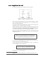
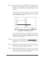
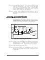
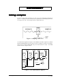
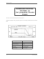
1
Communication Systems Modelling with Volume A1 Fundamental Analog Experiments Tim Hooper . Communication Systems Modelling with Volume A1 Fundamental Analog Experiments Emona Instruments Pty Ltd ABN 79 069-417-563 86 Parramatta Road Camperdown NSW 2050 Sydney AUSTRALIA is a registered trademark of Amberley Holdings Pty Ltd ABN 61 001-080-093 a company incorporated in the State of NSW AUSTRALIA WHAT IS TIMS ? TIMS is a Telecommunications Instructional Modelling System. models telecommunication systems. It Text books on telecommunications abound with block diagrams. These diagrams illustrate the subject being discussed by the author. Generally they are small sub-systems of a larger system. Their behaviour is described by the author with the help of mathematical equations, and with drawings or photographs of the signal waveforms expected to be present. TIMS brings alive the block diagram of the text book with a working model, recreating the waveforms on an oscilloscope. How can TIMS be expected to accommodate such a large number of models ? There may be hundreds of block diagrams in a text book, but only a relatively few individual block types. These block diagrams achieve their individuality because of the many ways a relatively few element types can be connected in different combinations. TIMS contains a collection of these block types, or modules, and there are very few block diagrams which it cannot model. PURPOSE OF TIMS TIMS can support courses in Telecommunications at all levels - from Technical Colleges through to graduate degree courses at Universities. This text is directed towards using TIMS as support for a course given at any level of teaching. Most early experiments are concerned with illustrating a small part of a larger system. Two or more of these sub-systems can be combined to build up a larger system. The list of possible experiments is limitless. Each instructor will have his or her own favourite collection - some of them are sure to be found herein. Naturally, for a full appreciation of the phenomena being investigated, there is no limit to the depth of mathematical analysis that can be undertaken. But most experiments can be performed successfully with little or no mathematical support. It is up to the instructor to decide the level of understanding that is required. EXPERIMENT AIMS The experiments in this Volume are concerned with introductory analog communications. Most of them require only the TIMS basic set of modules. The experiments have been written with the idea that each model examined could eventually become part of a larger telecommunications system, the aim of this large system being to transmit a message from input to output. The origin of this message, for the analog experiments in Volumes A1 and A2, would ultimately be speech. But for test and measurement purposes a sine wave, or perhaps two sinewaves (as in the two-tone test signal) are generally substituted. For the digital experiments (Volumes D1 and D2) the typical message is a pseudo random binary sequence. The experiments are designed to be completed in about two hours, with say one hour of preparation prior to the laboratory session. The four Volumes of Communication Systems Modelling with TIMS are: A1 - Fundamental Analog Experiments A2 - Further & Advanced Analog Experiments D1 - Fundamental Digital Experiments D2 - Further & Advanced Digital Experiments Contents Introduction to modelling with TIMS .............................................. 1 Modelling an equation ................................................................... 19 DSBSC generation ......................................................................... 33 Amplitude modulation ................................................................... 47 Envelopes....................................................................................... 69 Envelope recovery.......................................................................... 71 SSB generation - the phasing method ............................................ 83 Product demodulation - synch. & asynchronous............................ 97 SSB demodulation - the phasing method..................................... 109 The sampling theorem.................................................................. 121 PAM & time division multiplex .................................................. 137 Power measurements ................................................................... 145 Appendix A - Filter responses ...................................................... A1 Appendix B - Some Useful Expansions.........................................B1 INTRODUCTION TO MODELLING WITH TIMS model building.............................................................................2 why have patching diagrams ?....................................................................2 organization of experiments ........................................................3 who is running this experiment ?.................................................3 early experiments.........................................................................4 modulation..................................................................................................4 messages ......................................................................................4 analog messages .........................................................................................4 digital messages..........................................................................................5 bandwidths and spectra................................................................5 measurement...............................................................................................6 graphical conventions ..................................................................6 representation of spectra.............................................................................6 filters ..........................................................................................................8 other functions............................................................................................9 measuring instruments .................................................................9 the oscilloscope - time domain ...................................................................9 the rms voltmeter......................................................................................10 the spectrum analyser - frequency domain ...............................................10 oscilloscope - triggering ............................................................10 what you see, and what you don`t..............................................11 overload. ....................................................................................11 overload of a narrowband system.............................................................12 the two-tone test signal.............................................................................12 Fourier series and bandwidth estimation ...................................13 multipliers and modulators ........................................................13 multipliers ................................................................................................13 modulators................................................................................................14 envelopes ...................................................................................15 extremes.....................................................................................15 analog or digital ? ......................................................................15 SIN or COS ? .............................................................................16 the ADDER - G and g..............................................................16 abbreviations..............................................................................17 list of symbols............................................................................18 Introduction to modelling with TIMS Vol A1, ch 1, rev 1.0 - 1 INTRODUCTION TO MODELLING WITH TIMS model building With TIMS you will be building models. These models will most often be hardware realizations of the block diagrams you see in a text book, or have designed yourself. They will also be representations of equations, which themselves can be depicted in block diagram form. What ever the origin of the model, it can be patched up in a very short time. The next step is to adjust the model to perform as expected. It is perfectly true that you might, on occasions, be experimenting, or just ‘doodling’, not knowing what to expect. But in most cases your goal will be quite clear, and this is where a systematic approach is recommended. If you follow the steps detailed in the first few experiments you will find that the models are adjusted in a systematic manner, so that each desired result is obtained via a complete understanding of the purpose and aim of the intermediate steps leading up to it. why have patching diagrams ? Many of the analog experiments, and all of the digital experiments, display patching diagrams. These give all details of the interconnections between modules, to implement a model of the system under investigation. It is not expected that a glance at the patching diagram will reveal the nature of the system being modelled. The patching diagram is presented as firm evidence that a model of the system can be created with TIMS. The functional purpose of the system is revealed through the block diagram which precedes the patching diagram. 2 - A1 Introduction to modelling with TIMS It is the block diagram which you should study to gain insight into the workings of the system. If you fully understand the block diagram you should not need the patching diagram, except perhaps to confirm which modules are required for particular operations, and particular details of functionality. These is available in the TIMS User Manual. You may need an occasional glance at the patching diagram for confirmation of a particular point. Try to avoid patching up ‘mechanically’, according to the patching diagram, without thought to what you are trying to achieve. organization of experiments Each of the experiments in this Text is divided into three parts. 1. The first part is generally titled PREPARATION. This part should be studied before the accompanying laboratory session. 2. The second part describes the experiment proper. Its title will vary. You will find the experiment a much more satisfying experience if you arrive at the laboratory well prepared, rather than having to waste time finding out what has to be done at the last moment. Thus read this part before the laboratory session. 3. The third part consists of TUTORIAL QUESTIONS. Generally these questions will be answered after the experimental work is completed, but it is a good idea to read them before the laboratory session, in case there are special measurements to be made. While performing an experiment you should always have access to the TIMS user manuals - namely the TIMS User Manual (fawn cover) which contains information about the modules in the TIMS Basic Set of modules, and the TIMS Advanced Modules and TIMS Special Applications Modules User Manual (red cover). who is running this experiment ? These experiments and their Tasks are merely suggestions as to how you might go about carrying out certain investigations. In the final assessment it is you who are running the experiment, and you must make up your mind as to how you are going to do it. You can do this best if you read about it beforehand. If you do not understand a particular instruction, consider what it is you have been trying to achieve up to that point, and then do it your way. Introduction to modelling with TIMS A1 - 3 early experiments The first experiment assumes no prior knowledge of telecommunications - it is designed to introduce you to TIMS, and to illustrate the previous remarks about being systematic. The techniques learned will be applied over and over again in later work. The next few experiments are concerned with analog modulation and demodulation. modulation One of the many purposes of modulation is to convert a message into a form more suitable for transmission over a particular medium. The analog modulation methods to be studied will generally transform the analog message signal in the audio spectrum to a higher location in the frequency spectrum. The digital modulation methods to be studied will generally transform a binary data stream (the message), at baseband 1 frequencies, to a different format, and then may or may not translate the new form to a higher location in the frequency spectrum. It is much easier to radiate a high frequency (HF) signal than it is a relatively low frequency (LF) audio signal. In the TIMS environment the particular part of the spectrum chosen for HF signals is centred at 100 kHz. It is necessary, of course, that the reverse process, demodulation, can be carried out - namely, that the message may be recovered from the modulated signal upon receipt following transmission. messages Many models will be concerned with the transmission or reception of a message, or a signal carrying a message. So TIMS needs suitable messages. These will vary, depending on the system. analog messages The transmission of speech is often the objective in an analog system. High-fidelity speech covers a wide frequency range, say 50 Hz to 15 kHz, but for communications purposes it is sufficient to use only those components which lie in the audio frequency range 300 to 3000 Hz - this is called ‘band limited speech’. Note that frequency components have been removed from both the low and the high frequency end of the message spectrum. This is bandpass filtering. Intelligibility suffers if only the high frequencies are removed. Speech is not a convenient message signal with which to make simple and precise measurements. So, initially, a single tone (sine wave) is used. This signal is more easily accommodated by both the analytical tools and the instrumentation and measuring facilities. 1 defined later 4 - A1 Introduction to modelling with TIMS The frequency of this tone can be chosen to lie within the range expected in the speech, and its peak amplitude to match that of the speech. The simple tone can then be replaced by a two-tone test signal, in which case intermodulation tests can be carried out 2. When each modulation or demodulation system has been set up quantitatively using a single tone as a message (or, preferably with a two-tone test signal), a final qualitative check can be made by replacing the tone with a speech signal. The peak amplitude of the speech should be adjusted to match that of the tone. Both listening tests (in the case of demodulation) and visual examination of the waveforms can be very informative. digital messages The transmission of binary sequences is often the objective of a digital communication system. Of considerable interest is the degree of success with which this transmission is achieved. An almost universal method of describing the quality of transmission is by quoting an error rate 3. If the sequence is one which can take one of two levels, say 0 and 1, then an error is recorded if a 0 is received when a 1 was sent, or a 1 received when a 0 was sent. The bit error rate is measured as the number of errors as a proportion of total bits sent. To be able to make such a measurement it is necessary to know the exact nature of the original message. For this purpose a known sequence needs to be transmitted, a copy of which can be made available at the receiver for comparison purposes. The known sequence needs to have known, and useful, statistical properties - for example, a ‘random’ sequence. Rather simple generators can be implemented using shift registers, and these provide sequences of adjustable lengths. They are known as pseudo-random binary sequence (PRBS) generators. TIMS provides you with just such a SEQUENCE GENERATOR module. You should refer to a suitable text book for more information on these. bandwidths and spectra Most of the signals you will be examining in the experiments to follow have well defined bandwidths. That is, in most cases it is possible to state quite clearly that all of the energy of a signal lies between frequencies f1 and f2 Hz, where f1 < f2. • the absolute bandwidth of such a signal is defined as (f2 - f1) Hz. It is useful to define the number of octaves a signal occupies. The octave measure for the above signal is defined as octaves = log2(f2 / f1) Note that the octave measure is a function of the ratio of two frequencies; it says nothing about their absolute values. • a wideband signal is generally considered to be one which occupies one or more octaves. 2 the two-tone test signal is introduced in the experiment entitled ‘Amplifier overload’. 3 the corresponding measurement in an analog system would be the signal-to-noise ratio (relatively easy to measure with instruments), or, if speech is the message, the ‘intelligibility’; not so easy to define, let alone to measure. Introduction to modelling with TIMS A1 - 5 • a narrowband signal is one which occupies a small fraction of an octave. Another name, used interchangeably, is a bandpass signal. An important observation can be made about a narrowband signal; that is, it can contain no harmonics. • a baseband signal is one which extends from DC (so f1 = 0) to a finite frequency f2. It is thus a wideband signal. Speech, for communications, is generally bandlimited to the range 300 to 3000 Hz. It thus has a bandwidth in excess of 3 octaves. This is considered to be a wideband signal. After modulation, to a higher part of the spectrum, it becomes a narrowband signal, but note that its absolute bandwidth remains unchanged. This reduction from a wideband to a narrowband signal is a linear process; it can be reversed. In the context of communications engineering it involves modulation, or frequency translation. You will meet all of these signals and phenomena when working with TIMS. measurement The bandwidth of a signal can be measured with a SPECTRUM ANALYSER. Commercially available instruments typically cover a wide frequency range, are very accurate, and can perform a large number of complex measurements. They are correspondingly expensive. TIMS has no spectrum analyser as such, but can model one (with the TIMS320 DSP module), or in the form of a simple WAVE ANALYSER with TIMS analog modules. See the experiment entitled Spectrum analysis - the WAVE ANALYSER (within Volume A2 - Further & Advanced Analog Experiments). Without a spectrum analyser it is still possible to draw conclusions about the location of a spectrum, by noticing the results when attempting to pass it through filters of different bandwidths. There are several filters in the TIMS range of modules. See Appendix A, and also the TIMS User Manual. graphical conventions representation of spectra It is convenient to have a graphical method of depicting spectra. In this work we do not get involved with the Fourier transform, with its positive and negative frequencies and double sided spectra. Elementary trigonometrical methods are used for analysis. Such methods are more than adequate for our purposes. When dealing with speech the mathematical analysis is dropped, and descriptive methods used. These are supported by graphical representations of the signals and their spectra. In the context of modulation we are constantly dealing with sidebands, generally derived from a baseband message of finite bandwidth. Such finite bandwidth signals will be represented by triangles on the spectral diagrams. The steepness of the slope of the triangle has no special significance, although when two or more sidebands, from different messages, need to be distinguished, each can be given a different slope. 6 - A1 Introduction to modelling with TIMS frequency a baseband signal (eg., a message) Although speech does not have a DC component, the triangle generally extends down to zero (the origin) of the frequency scale (rather than being truncated just before it). For the special case in which a baseband signal does have a DC component the triangle convention is sometimes modified slightly by adding a vertical line at the zero-frequency end of the triangle. a DSBSC The direction of the slope is important. Its significance becomes obvious when we wish to draw a modulated signal. The figure above shows a double sideband suppressed carrier (DSBSC) signal. Note that there are TWO triangles, representing the individual lower and upper sidebands. They slope towards the same point; this point indicates the location of the (suppressed) carrier frequency. an inverted baseband signal The orientation is important. If the same message was so modulated that it could be represented in the frequency spectrum as in the figure above, then this means: • • the signal is located in the baseband part of the spectrum • since the signal is at baseband it would be audible (if converted with an electric to acoustic transducer - a pair of headphones, for example), but would be unintelligible. You will be able to listen to this and other such signals in TIMS experiments to come. spectral components have been transposed, or inverted; frequency components which were originally above others are now below them. It is common practice to use the terms erect and inverted to describe these bands. Introduction to modelling with TIMS A1 - 7 In the Figure above, a message (a) is frequency translated to become an upper single sideband (b), and a lower single sideband (c). A three-channel frequency division multiplexed (FDM) signal is also illustrated (d). Note that these spectral diagrams do not show any phase information. Despite all the above, be prepared to accept that these diagrams are used for purposes of illustration, and different authors use their own variations. For example, some slope their triangles in the opposite sense to that suggested here. filters In a block diagram, there is a simple technique for representing filters. The frequency spectrum is divided into three bands - low, middle, and high - each represented by part of a sinewave. If a particular band is blocked, then this is indicated by an oblique stroke through it. The standard responses are represented as in the Figure below. block-diagrammatic representations of filter responses The filters are, respectively, lowpass, bandpass, highpass, bandstop, and allpass. In the case of lowpass and highpass responses the diagrams are often further simplified by the removal of one of the cancelled sinewaves, the result being as in the figure opposite. 8 - A1 Introduction to modelling with TIMS other functions amplify add multiply amplitude limit integrate some analog functions measuring instruments the oscilloscope - time domain The most frequently used measuring facility with TIMS is the oscilloscope. In fact the vast majority of experiments can be satisfactorily completed with no other instrument. Any general purpose oscilloscope is ideal for all TIMS experiments. It is intended for the display of signals in the time domain 4. It shows their waveforms - their shapes, and amplitudes From the display can be obtained information regarding: • • • • • waveform shape waveform frequency - by calculation, using time base information waveform amplitude - directly from the display system linearity - by observing waveform distortion an estimate of the bandwidth of a complex signal; eg, from the sharpness of the corners of a square wave When concerned with amplitude information it is customary to record either: • • the peak-to-peak amplitude the peak amplitude of the waveform visible on the screen. Unless the waveform is a simple sinewave it is always important to record the shape of the waveform also; this can be: 1. as a sketch (with time scale), and annotation to show clearly what amplitude has been measured. 2. as an analytic expression, in which case the parameter recorded must be clearly specified. 4 but with adaptive circuitry it can be modified to display frequency-domain information Introduction to modelling with TIMS A1 - 9 the rms voltmeter The TIMS WIDEBAND TRUE RMS METER module is essential for measurements concerning power, except perhaps for the simple case when the signal is one or two sinewaves. It is particularly important when the measurement involves noise. Its bandwidth is adequate for all of the signals you will meet in the TIMS environment. An experiment which introduces the WIDEBAND TRUE RMS METER, is entitled Power measurements. Although it appears at the end of this Volume, it could well be attempted at almost any time. the spectrum analyser - frequency domain The identification of the spectral composition of a signal - its components in the frequency domain - plays an important part when learning about communications. Unfortunately, instruments for displaying spectra tend to be far more expensive than the general purpose oscilloscope. It is possible to identify and measure the individual spectral components of a signal using TIMS modules. Instruments which identify the spectral components on a component-bycomponent basis are generally called wave analysers. A model of such an instrument is examined in the experiment entitled Spectrum analysis - the WAVE ANALYSER in Volume A2 - Further & Advanced Analog Experiments. Instruments which identify the spectral components of a signal and display the spectrum are generally called spectrum analysers. These instruments tend to be more expensive than wave analysers. Something more sophisticated is required for their modelling, but this is still possible with TIMS, using the digital signals processing (DSP) facilities - the TIMS320 module can be programmed to provide spectrum analysis facilities. Alternatively the distributors of TIMS can recommend other affordable methods, compatible with the TIMS environment. oscilloscope - triggering synchronization As is usually the case, to achieve ‘text book like’ displays, it is important to choose an appropriate signal for oscilloscope triggering. This trigger signal is almost never the signal being observed ! The recognition of this point is an important step in achieving stable displays. This chosen triggering signal should be connected directly to the oscilloscope sweep synchronizing circuitry. Access to this circuitry of the oscilloscope is available via an input socket other than the vertical deflection amplifier input(s). It is typically labelled ‘ext. trig’ (external trigger), ‘ext. synch’ (external synchronization), or similar. sub-multiple frequencies If two or more periodic waveforms are involved, they will only remain stationary with respect to each other if the frequency of one is a sub-multiple of the other. 10 - A1 Introduction to modelling with TIMS This is seldom the case in practice, but can be made so in the laboratory. Thus TIMS provides, at the MASTER SIGNALS module, a signal of 2.083 kHz (which is 1/48 of the 100 kHz system clock), and another at 8.333 kHz (1/12 of the system clock). which channel ? Much time can be saved if a consistent use of the SCOPE SELECTOR is made. This enables quick changes from one display to another with the flip of a switch. In addition, channel identification is simplified if the habit is adopted of consistently locating the trace for CH1 above the trace for CH2. Colour coded patching leads can also speed trace identification. what you see, and what you don`t Instructions such as ‘adjust the phase until there is no output’, or ‘remove the unwanted signal with a suitable filter’ will be met from time to time. These instructions seldom result in the amplitude of the signal in question being reduced to zero. Instead, what is generally meant is ‘reduce the amplitude of the signal until it is no longer of any significance’. Significance here is a relative term, made with respect to the system signal-tonoise ratio (SNR). All systems have a background noise level (noise threshold, noise floor), and signals (wanted) within these systems must over-ride this noise (unwanted). TIMS is designed to have a ‘working level’, the TIMS ANALOG REFERENCE LEVEL, of about 4 volts peak-to-peak. The system noise level is claimed to be at least 100 times below this 5. When using an oscilloscope as a measuring instrument with TIMS, the vertical sensitivity is typically set to about 1 volt/cm. Signals at the reference level fit nicely on the screen. If they are too small it is wise to increase them if possible (and appropriate), to over-ride the system noise; or if larger to reduce them, to avoid system overload. When they are attenuated by a factor of 100, and if the oscilloscope sensitivity is not changed, they appear to be ‘reduced to zero’; and in relative terms this is so. If the sensitivity of the oscilloscope is increased by 100, however, the screen will no longer be empty. There will be the system noise, and perhaps the signal of interest is still visible. Engineering judgement must then be exercised to evaluate the significance of the signals remaining. overload If wanted signal levels within a system fall ‘too low’ in amplitude, then the signalto-noise ratio (SNR) will suffer, since internal circuit noise is independent of signal level. If signal levels within a system rise ‘too high’, then the SNR will suffer, since the circuitry will overload, and generate extra, unwanted, distortion components; these distortion components are signal level dependent. In this case the noise is 5 TIMS claims a system signal-to-noise ratio of better than 40 dB Introduction to modelling with TIMS A1 - 11 derived from distortion of the signal, and the degree of distortion is usually quoted as signal-to-distortion ratio (SDR). Thus analog circuit design includes the need to maintain signal levels at a predefined working level, being ‘not to high’ and ‘not too low’, to avoid these two extremes. These factors are examined in the experiment entitled Amplifier overload within Volume A2 - Further & Advanced Analog Experiments. The TIMS working signal level, or TIMS ANALOG REFERENCE LEVEL, has been set at 4 volts peak-to-peak. Modules will generally run into non-linear operation when this level is exceeded by say a factor of two. The background noise of the TIMS system is held below about 10 mV - this is a fairly loose statement, since this level is dependent upon the bandwidth over which the noise is measured, and the model being examined at the time. A general statement would be to say that TIMS endeavours to maintain a SNR of better than 40 dB for all models. overload of a narrowband system Suppose a channel is narrowband. This means it is deliberately bandlimited so that it passes signals in a narrow (typically much less than an octave 6) frequency range only. There are many such circuits in a communications system. If this system overloads on a single tone input, there will be unwanted harmonics generated. But these will not pass to the output, and so the overload may go unnoticed. With a more complex input - say two or more tones, or a speechrelated signal - there will be, in addition, unwanted intermodulation components generated. Many of these will pass via the system, thus revealing the existence of overload. In fact, the two-tone test signal should always be used in a narrowband system to investigate overload. the two-tone test signal A two-tone test signal consists of two sine waves added together ! As discussed in the previous section, it is a very useful signal for testing systems, especially those which are of narrow-bandwidth. The properties of the signal depend upon: • • the frequency ratio of the two tones. the amplitude ratio of the two tones. For testing narrowband communication systems the two tones are typically of near-equal frequency, and of identical amplitude. A special property of this form of the signal is that its shape, as seen in the time domain, is very well defined and easily recognisable 7. After having completed the early experiments you will recognise this shape as that of the double sideband suppressed carrier (DSBSC) signal. If the system through which this signal is transmitted has a non-linear transmission characteristic, then this will generate extra components. The presence of even small amounts of these components is revealed by a change of shape of the test signal. 6 defined above 7 the assumption being that the oscilloscope is set to sweep across the screen over a few periods of the difference frequency. 12 - A1 Introduction to modelling with TIMS Fourier series and bandwidth estimation Fourier series analysis of periodic signals reveals that: • it is possible, by studying the symmetry of a signal, to predict the presence or absence of a DC component. • if a signal is other than sinusoidal, it will contain more than one harmonic component of significance. • if a signal has sharp discontinuities, it is likely to contain many harmonic components of significance • some special symmetries result in all (or nearly all) of the ODD (or EVEN) harmonics being absent. With these observations, and more, it is generally easy to make an engineering estimate of the bandwidth of a periodic signal. multipliers and modulators The modulation process requires multiplication. But a pure MULTIPLIER is seldom found in communications equipment. Instead, a device called a MODULATOR is used. In the TIMS system we generally use a MULTIPLIER, rather than a MODULATOR, when multiplication is called for, so as not to become diverted by the side effects and restrictions imposed by the latter. In commercial practice, however, the purpose-designed MODULATOR is generally far superior to the unnecessarily versatile MULTIPLIER. multipliers An ideal multiplier performs as a multiplier should ! That is, if the two timedomain functions x(t) and y(t) are multiplied together, then we expect the result to be x(t).y(t), no more and no less, and no matter what the nature of these two functions. These devices are called four quadrant multipliers. There are practical multipliers which approach this ideal, with one or two engineering qualifications. Firstly, there is always a restriction on the bandwidth of the signals x(t) and y(t). There will inevitably be extra (unwanted) terms in the output (noise, and particularly distortion products) due to practical imperfections. Provided these unwanted terms can be considered ‘insignificant’, with respect to the magnitude of the wanted terms, then the multiplier is said to be ‘ideal’. In the TIMS environment this means they are at least 40 dB below the TIMS ANALOG REFERENCE LEVEL 8. Such a multiplier is even said to be linear. That is, from an engineering point of view, it is performing as expected. 8 defined under ‘what you see and what you don`t’ Introduction to modelling with TIMS A1 - 13 In the mathematical sense it is not linear, since the mathematical definition of a linear circuit includes the requirement that no new frequency components are generated when it performs its normal function. But, as will be seen, multiplication always generates new frequency components. DC off-sets One of the problems associated with analog circuit design is minimization of unwanted DC off-sets. If the signals to be processed have no DC component (such as in an audio system) then stages can be AC coupled, and the problem is overcome. In the TIMS environment module bandwidths must extend to DC, to cope with all possible conditions; although more often than not signals have no intentional DC component. In a complex model DC offsets can accumulate - but in most cases they can be recognised as such, and accounted for appropriately. There is one situation, however, where they can cause much more serious problems by generating new components - and that is when multiplication is involved. With a MULTIPLIER the presence of an unintentional DC component at one input will produce new components at the output. Specifically, each component at the other input will be multiplied by this DC component - a constant - and so a scaled version will appear at the output 9. To overcome this problem there is an option for AC coupling in the MULTIPLIER module. It is suggested that the DC mode be chosen only when the signals to be processed actually have DC components; otherwise use AC coupling. modulators In communications practice the circuitry used for the purpose of performing the multiplying function is not always ideal in the four quadrant multiplier sense; such circuits are generally called modulators. Modulators generate the wanted sum or difference products but in many cases the input signals will also be found in the output, along with other unwanted components at significant levels. Filters are used to remove these unwanted components from the output (alternatively there are ‘balanced’ modulators. These have managed to eliminate either one or both of the original signals from the output). These modulators are restricted in other senses as well. It is allowed that one of the inputs can be complex (ie., two or more components) but the other can only be a single frequency component (or appear so to be - as in the switching modulator). This restriction is of no disadvantage, since the vast majority of modulators are required to multiply a complex signal by a single-component carrier. Accepting restrictions in some areas generally results in superior performance in others, so that in practice it is the switching modulator, rather than the idealized four quadrant multiplier, which finds universal use in communications electronics. Despite the above, TIMS uses the four quadrant multiplier in most applications where a modulator might be used in practice. This is made possible by the relatively low frequency of operation, and modest linearity requirements 9 this is the basis of a voltage controlled amplifier - VCA 14 - A1 Introduction to modelling with TIMS envelopes Every narrowband signal has an envelope, and you probably have an idea of what this means. Envelopes will be examined first in the experiment entitled DSB generation in this Volume. They will be defined and further investigated in the experiments entitled Envelopes within this Volume, and Envelope recovery within Volume A2 Further & Advanced Analog Experiments. extremes Except for a possible frequency scaling effect, most experiments with TIMS will involve realistic models of the systems they are emulating. Thus message frequencies will be ‘low’, and carrier frequencies ‘high’. But these conditions need not be maintained. TIMS is a very flexible environment. It is always a rewarding intellectual exercise to imagine what would happen if one or more of the ‘normal’ conditions was changed severely 10. It is then even more rewarding to confirm our imaginings by actually modelling these unusual conditions. TIMS is sufficiently flexible to enable this to be done in most cases. For example: it is frequently stated, for such-and-such a requirement to be satisfied, that it is necessary that ‘x1 >> x2’. Quite often x1 and x2 are frequencies - say a carrier and a message frequency; or they could be amplitudes. You are strongly encouraged to expand your horizons by questioning the reasons for specifying the conditions, or restrictions, within a model, and to consider, and then examine, the possibilities when they are ignored. analog or digital ? What is the difference between a digital signal and an analog signal ? Sometimes this is not clear or obvious. In TIMS digital signals are generally thought of as those being compatible with the TTL standards. Thus their amplitudes lie in the range 0 to +5 volts. They come from, and are processed by, modules having RED output and input sockets. It is sometimes necessary, however, to use an analog filter to bandlimit these signals. But their large DC offsets would overload most analog modules, . Some digital modules (eg, the SEQUENCE GENERATOR) have anticipated this, and provide an analog as well as a digital (TTL) output. This analog output comes 10 for an entertaining and enlightening look at the effects of major changes to one or more of the physical constants, see G. Gamow; Mr Tompkins in Wonderland published in 1940, or easier Mr. Tompkins in Paperback, Cambridge University Press, 1965. Introduction to modelling with TIMS A1 - 15 from a YELLOW socket, and is a TTL signal with the DC component removed (ie, DC shifted). SIN or COS ? Single frequency signals are generally referred to as sinusoids, yet when manipulating them trigonometrically are often written as cosines. How do we obtain cosωt from a sinusoidal oscillator ! There is no difference in the shape of a sinusoid and a cosinusoid, as observed with an oscilloscope. A sinusoidal oscillator can just as easily be used to provide a cosinusoid. What we call the signal (sin or cos) will depend upon the time reference chosen. Remember that cosωt = sin(ωt + π/2) Often the time reference is of little significance, and so we choose sin or cos, in any analysis, as is convenient. the ADDER - G and g Refer to the TIMS User Manual for a description of the ADDER module. Notice it has two input sockets, labelled ‘A’ and ‘B’. In many experiments an ADDER is used to make a linear sum of two signals a(t) and b(t), of amplitudes A and B respectively, connected to the inputs A and B respectively. The proportions of these signals which appear at the ADDER output are controlled by the front panel gain controls G and g. The amplitudes A and B of the two input signals are seldom measured, nor the magnitudes G and g of the adjustable gains. Instead it is the magnitudes GA and gB which are of more interest, and these are measured directly at the ADDER output. The measurement of GA is made when the patch lead for input B is removed; and that of gB is measured when the patch lead for input A is removed. When referring to the two inputs in this text it would be formally correct to name them as ‘the input A’ and ‘the input B’. This is seldom done. Instead, they are generally referred to as ‘the input G’ and ‘the input g’ respectively (or sometimes just G and g). This should never cause any misunderstanding. If it does, then it is up to you, as the experimenter, to make an intelligent interpretation. 16 - A1 Introduction to modelling with TIMS abbreviations This list is not exhaustive. It includes only those abbreviations used in this Text. abbreviation AM ASK BPSK CDMA CRO dB DPCM DPSK DSB DSBSC DSSS DUT ext. synch. ext. trig. FM FSK FSD IP ISB ISI LSB MSB NBFM OOK PAM PCM PDM PM PPM PRK PSK PWM SDR SNR SSB SSBSC SSR TDM THD VCA WBFM Introduction to modelling with TIMS meaning amplitude modulation amplitude shift keying (also called OOK) binary phase shift keying code division multiple access cathode ray oscilloscope decibel differential pulse code modulation differential phase shift keying double sideband (in this text synonymous with DSBSC) double sideband suppressed carrier direct sequence spread spectrum device under test external synchronization (of oscilloscope). ‘ext. trig.’ preferred external trigger (of an oscilloscope) frequency modulation frequency shift keying full scale deflection (of a meter, for example) intermodulation product independent sideband intersymbol interference analog: lower sideband digital: least significant bit most significant bit narrow band frequency modulation on-off keying (also called ASK) pulse amplitude modulation pulse code modulation pulse duration modulation (see PWM) phase modulation pulse position modulation phase reversal keying (also called PSK) phase shift keying (also called PRK - see BPSK) pulse width modulation (see PDM) signal-to-distortion ratio signal-to-noise ratio single sideband (in this text is synonymous with SSBSC) single sideband suppressed carrier sideband suppression ratio time division multiplex total harmonic distortion voltage controlled amplifier wide band frequency modulation A1 - 17 list of symbols The following symbols are used throughout the text, and have the following meanings a(t) a time varying amplitude α, φ, ϕ, phase angles β deviation, in context of PM and FM δf a small frequency increment ∆φ δt φ(t) peak phase deviation a small time interval a time varying phase m in the context of envelope modulation, the depth of modulation µ a low frequency (rad/s); typically that of a message (µ << ω). ω a high frequency (rad/s); typically that of a carrier (ω >> µ) y(t) 18 - A1 a time varying function Introduction to modelling with TIMS MODELLING AN EQUATION PREPARATION................................................................................. 20 an equation to model ................................................................. 20 the ADDER ..............................................................................................21 conditions for a null .................................................................................22 more insight into the null..........................................................................23 TIMS experiment procedures.................................................... 24 EXPERIMENT ................................................................................... 25 signal-to-noise ratio..................................................................................30 achievements ............................................................................. 30 as time permits .......................................................................... 31 TUTORIAL QUESTIONS ................................................................. 31 TRUNKS................................................................................... 32 Modelling an equation Vol A1, ch 2, ver 1.0 - 19 MODELLING AN EQUATION ACHIEVEMENTS: a familiarity with the TIMS modelling philosophy; development of modelling and experimental skills for use in future experiments. Introduction to the ADDER, AUDIO OSCILLATOR, and PHASE SHIFTER modules; also use of the SCOPE SELECTOR and FREQUENCY COUNTER. PREREQUISITES: a desire to enhance one’s knowledge of, and insights into, the phenomena of telecommunications theory and practice. PREPARATION This experiment assumes no prior knowledge of telecommunications. It illustrates how TIMS is used to model a mathematical equation. You will learn some experimental techniques. It will serve to introduce you to the TIMS system, and prepare you for the more serious experiments to follow. In this experiment you will model a simple trigonometrical equation. That is, you will demonstrate in hardware something with which you are already familiar analytically. an equation to model You will see that what you are to do experimentally is to demonstrate that two AC signals of the same frequency, equal amplitude and opposite phase, when added, will sum to zero. This process is used frequently in communication electronics as a means of removing, or at least minimizing, unwanted components in a system. You will meet it in later experiments. The equation which you are going to model is: y(t) = V1 sin(2πf1t) + V2 sin(2πf2t + α) = v1(t) + v2(t) ........ 1 ........ 2 Here y(t) is described as the sum of two sine waves. Every young trigonometrician knows that, if: ........ 3 each is of the same frequency: f1 = f2 Hz ........ 4 each is of the same amplitude: V1 = V2 volts 20 - A1 Modelling an equation and they are 180o out of phase: ........ 5 α = 180 degrees then: ........ 6 y(t) = 0 A block diagram to represent eqn.(1) is suggested in Figure 1. SOURCE ADDER v1 (t) OUT y(t) V sin2 πf1t -1 INVERTING AMPLIFIER v (t) 2 Figure 1: block diagram model of Equation 1 Note that we ensure the two signals are of the same frequency (f1 = f2) by obtaining them from the same source. The 180 degree phase change is achieved with an inverting amplifier, of unity gain. In the block diagram of Figure 1 it is assumed, by convention, that the ADDER has unity gain between each input and the output. Thus the output is y(t) of eqn.(2). This diagram appears to satisfy the requirements for obtaining a null at the output. Now see how we could model it with TIMS modules. A suitable arrangement is illustrated in block diagram form in Figure 2. OSCILLOSCOPE and FREQUENCY COUNTER connections not shown. v (t) 2 y(t) = g.v1(t) + G.v2(t) v (t) 1 = V sin2π f1t + V2 sin2πf2t 1 Figure 2: the TIMS model of Figure 1. Before you build this model with TIMS modules let us consider the procedure you might follow in performing the experiment. the ADDER The annotation for the ADDER needs explanation. The symbol ‘G’ near input A means the signal at this input will appear at the output, amplified by a factor ‘G’. Similar remarks apply to the input labelled ‘g’. Both ‘G’ and ‘g’ are adjustable by adjacent controls on the front panel of the ADDER. But note that, like the controls Modelling an equation A1 - 21 on all of the other TIMS modules, these controls are not calibrated. You must adjust these gains for a desired final result by measurement. Thus the ADDER output is not identical with eqn.(2), but instead: ADDER output = g.v1(t) + G.v2(t) = V1 sin2πf1t + V2 sin2πf2t ........ 7 ........ 8 conditions for a null For a null at the output, sometimes referred to as a ‘balance’, one would be excused for thinking that: if: 1) the PHASE SHIFTER is adjusted to introduce a difference of 180o between its input and output and 2) the gains ‘g’ and ‘G’ are adjusted to equality then 3) the amplitude of the output signal y(t) will be zero. In practice the above procedure will almost certainly not result in zero output ! Here is the first important observation about the practical modelling of a theoretical concept. In a practical system there are inevitably small impairments to be accounted for. For example, the gain through the PHASE SHIFTER is approximately unity, not exactly so. It would thus be pointless to set the gains ‘g’ and ‘G’ to be precisely equal. Likewise it would be a waste of time to use an expensive phase meter to set the PHASE SHIFTER to exactly 180o, since there are always small phase shifts not accounted for elsewhere in the model. See Q1, Tutorial Questions, at the end of this experiment. These small impairments are unknown, but they are stable. Once compensated for they produce no further problems. So we do not make precise adjustments to modules, independently of the system into which they will be incorporated, and then patch them together and expect the system to behave. All adjustments are made to the system as a whole to bring about the desired end result. The null at the output of the simple system of Figure 2 is achieved by adjusting the uncalibrated controls of the ADDER and of the PHASE SHIFTER. Although equations (3), (4), and (5) define the necessary conditions for a null, they do not give any guidance as to how to achieve these conditions. 22 - A1 Modelling an equation more insight into the null It is instructive to express eqn. (1) in phasor form. Refer to Figure 3. Figure 3: Equation (1) in phasor form Figure 3 (a) and (b) shows the phasors V1 and V2 at two different angles α. It is clear that, to minimise the length of the resultant phasor (V1 + V2), the angle α in (b) needs to be increased by about 45o. The resultant having reached a minimum, then V2 must be increased to approach the magnitude of V1 for an even smaller (finally zero) resultant. We knew that already. What is clarified is the condition prior to the null being achieved. Note that, as angle α is rotated through a full 360o, the resultant (V1 + V2) goes through one minimum and one maximum (refer to the TIMS User Manual to see what sort of phase range is available from the PHASE SHIFTER). What is also clear from the phasor diagram is that, when V1 and V2 differ by more than about 2:1 in magnitude, the minimum will be shallow, and the maximum broad and not pronounced 1. Thus we can conclude that, unless the magnitudes V1 and V2 are already reasonably close, it may be difficult to find the null by rotating the phase control. So, as a first step towards finding the null, it would be wise to set V2 close to V1. This will be done in the procedures detailed below. Note that, for balance, it is the ratio of the magnitudes V1 and V2 , rather than their absolute magnitudes, which is of importance. So we will consider V1 of fixed magnitude (the reference), and make all adjustments to V2. This assumes V1 is not of zero amplitude ! 1 fix V as reference; mentally rotate the phasor for V . The dashed circle shows the locus of its 1 2 extremity. Modelling an equation A1 - 23 TIMS experiment procedures. In each experiment the tasks ‘T’ you are expected to perform, and the questions ‘Q’ you are expected to answer, are printed in italics and in slightly larger characters than the rest of the text. In the early experiments there will a large list of tasks, each given in considerable detail. Later, you will not need such precise instructions, and only the major steps will be itemised. You are expected to become familiar with the capabilities of your oscilloscope, and especially with synchronization techniques. 24 - A1 Modelling an equation EXPERIMENT You are now ready to model eqn. (1). The modelling is explained step-by-step as a series of small tasks. Take these tasks seriously, now and in later experiments, and TIMS will provide you with hours of stimulating experiences in telecommunications and beyond. The tasks are identified with a ‘T’, are numbered sequentially, and should be performed in the order given. T1 both channels of the oscilloscope should be permanently connected to the matching coaxial connectors on the SCOPE SELECTOR. See the TIMS User Manual for details of this module. T2 in this experiment you will be using three plug-in modules, namely: an AUDIO OSCILLATOR, a PHASE SHIFTER, and an ADDER. Obtain one each of these. Identify their various features as described in the TIMS User Manual. Most modules can be controlled entirely from their front panels, but some have switches mounted on their circuit boards. Set these switches before plugging the modules into the TIMS SYSTEM UNIT; they will seldom require changing during the course of an experiment. T3 set the on-board range switch of the PHASE SHIFTER to ‘LO’. Its circuitry is designed to give a wide phase shift in either the audio frequency range (LO), or the 100 kHz range (HI). Modules can be inserted into any one of the twelve available slots in the TIMS SYSTEM UNIT. Choose their locations to suit yourself. Typically one would try to match their relative locations as shown in the block diagram being modelled. Once plugged in, modules are in an operating condition. T4 plug the three modules into the TIMS SYSTEM UNIT. T5 set the front panel switch of the FREQUENCY COUNTER to a GATE TIME of 1s. This is the most common selection for measuring frequency. When you become more familiar with TIMS you may choose to associate certain signals with particular patch lead colours. For the present, choose any colour which takes your fancy. Modelling an equation A1 - 25 T6 connect a patch lead from the lower yellow (analog) output of the AUDIO OSCILLATOR to the ANALOG input of the FREQUENCY COUNTER. The display will indicate the oscillator frequency f1 in kilohertz (kHz). T7 set the frequency f1 with the knob on the front panel of the AUDIO OSCILLATOR, to approximately 1 kHz (any frequency would in fact be suitable for this experiment). T8 connect a patch lead from the upper yellow (analog) output of the AUDIO OSCILLATOR to the ‘ext. trig’ [ or ‘ext. synch’ ] terminal of the oscilloscope. Make sure the oscilloscope controls are switched so as to accept this external trigger signal; use the automatic sweep mode if it is available. T9 set the sweep speed of the oscilloscope to 0.5 ms/cm. T10 patch a lead from the lower analog output of the AUDIO OSCILLATOR to the input of the PHASE SHIFTER. T11 patch a lead from the output of the PHASE SHIFTER to the input G of the ADDER 2. T12 patch a lead from the lower analog output of the AUDIO OSCILLATOR to the input g of the ADDER. T13 patch a lead from the input g of the ADDER to CH2-A of the SCOPE SELECTOR module. Set the lower toggle switch of the SCOPE SELECTOR to UP. T14 patch a lead from the input G of the ADDER to CH1-A of the SCOPE SELECTOR. Set the upper SCOPE SELECTOR toggle switch UP. T15 patch a lead from the output of the ADDER to CH1-B of the SCOPE SELECTOR. This signal, y(t), will be examined later on. Your model should be the same as that shown in Figure 4 below, which is based on Figure 2. Note that in future experiments the format of Figure 2 will be used for TIMS models, rather than the more illustrative and informal style of Figure 4, which depicts the actual flexible patching leads. You are now ready to set up some signal levels. 2 the input is labelled ‘A’, and the gain is ‘G’. This is often called ‘the input G’; likewise ‘input g’. 26 - A1 Modelling an equation v (t) 2 v (t) 1 Figure 4: the TIMS model. T16 find the sinewave on CH1-A and, using the oscilloscope controls, place it in the upper half of the screen. T17 find the sinewave on CH2-A and, using the oscilloscope controls, place it in the lower half of the screen. This will display, throughout the experiment, a constant amplitude sine wave, and act as a monitor on the signal you are working with. Two signals will be displayed. These are the signals connected to the two ADDER inputs. One goes via the PHASE SHIFTER, which has a gain whose nominal value is unity; the other is a direct connection. They will be of the same nominal amplitude. T18 vary the COARSE control of the PHASE SHIFTER, and show that the relative phases of these two signals may be adjusted. Observe the effect of the ±1800 toggle switch on the front panel of the PHASE SHIFTER. As part of the plan outlined previously it is now necessary to set the amplitudes of the two signals at the output of the ADDER to approximate equality. Comparison of eqn. (1) with Figure 2 will show that the ADDER gain control g will adjust V1, and G will adjust V2. You should set both V1 and V2, which are the magnitudes of the two signals at the ADDER output, at or near the TIMS ANALOG REFERENCE LEVEL, namely 4 volt peak-to-peak. Now let us look at these two signals at the output of the ADDER. T19 switch the SCOPE SELECTOR from CH1-A to CH1-B. Channel 1 (upper trace) is now displaying the ADDER output. T20 remove the patch cords from the g input of the ADDER. This sets the amplitude V1 at the ADDER output to zero; it will not influence the adjustment of G. Modelling an equation A1 - 27 T21 adjust the G gain control of the ADDER until the signal at the output of the ADDER, displayed on CH1-B of the oscilloscope, is about 4 volt peakto-peak. This is V2. T22 remove the patch cord from the G input of the ADDER. This sets the V2 output from the ADDER to zero, and so it will not influence the adjustment of g. T23 replace the patch cords previously removed from the g input of the ADDER, thus restoring V1. T24 adjust the g gain control of the ADDER until the signal at the output of the ADDER, displayed on CH1-B of the oscilloscope, is about 4 volt peakto-peak. This is V1. T25 replace the patch cords previously removed from the G input of the ADDER. Both signals (amplitudes V1 and V2) are now displayed on the upper half of the screen (CH1-B). Their individual amplitudes have been made approximately equal. Their algebraic sum may lie anywhere between zero and 8 volt peak-to-peak, depending on the value of the phase angle α. It is true that 8 volt peak-to-peak would be in excess of the TIMS ANALOG REFERENCE LEVEL, but it won`t overload the oscilloscope, and in any case will soon be reduced to a null. Your task is to adjust the model for a null at the ADDER output, as displayed on CH1-B of the oscilloscope. You may be inclined to fiddle, in a haphazard manner, with the few front panel controls available, and hope that before long a null will be achieved. You may be successful in a few moments, but this is unlikely. Such an approach is definitely not recommended if you wish to develop good experimental practices. Instead, you are advised to remember the plan discussed above. This should lead you straight to the wanted result with confidence, and the satisfaction that instant and certain success can give. There are only three conditions to be met, as defined by equations (3), (4), and (5). • the first of these is already assured, since the two signals are coming from a common oscillator. • the second is approximately met, since the gains ‘g’ and ‘G’ have been adjusted to make V1 and V2, at the ADDER output, about equal. • the third is unknown, since the front panel control of the PHASE SHIFTER is not calibrated 3. It would thus seem a good idea to start by adjusting the phase angle α. So: 3 TIMS philosophy is not to calibrate any controls. In this case it would not be practical, since the phase range of the PHASE SHIFTER varies with frequency. 28 - A1 Modelling an equation T26 set the FINE control of the PHASE SHIFTER to its central position. T27 whilst watching the upper trace, y(t) on CH1-B, vary the COARSE control of the PHASE SHIFTER. Unless the system is at the null or maximum already, rotation in one direction will increase the amplitude, whilst in the other will reduce it. Continue in the direction which produces a decrease, until a minimum is reached. That is, when further rotation in the same direction changes the reduction to an increase. If such a minimum can not be found before the full travel of the COARSE control is reached, then reverse the front panel 180O TOGGLE SWITCH, and repeat the procedure. Keep increasing the sensitivity of the oscilloscope CH1 amplifier, as necessary, to maintain a convenient display of y(t). Leave the PHASE SHIFTER controls in the position which gives the minimum. T28 now select the G control on the ADDER front panel to vary V2, and rotate it in the direction which produces a deeper null. Since V1 and V2 have already been made almost equal, only a small change should be necessary. T29 repeating the previous two tasks a few times should further improve the depth of the null. As the null is approached, it will be found easier to use the FINE control of the PHASE SHIFTER. These adjustments (of amplitude and phase) are NOT interactive, so you should reach your final result after only a few such repetitions. Nulling of the two signals is complete ! You have achieved your first objective You will note that it is not possible to achieve zero output from the ADDER. This never happens in a practical system. Although it is possible to reduce y(t) to zero, this cannot be observed, since it is masked by the inevitable system noise. T30 reverse the position of the PHASE SHIFTER toggle switch. Record the amplitude of y(t), which is now the absolute sum of V1 PLUS V2. Set this signal to fill the upper half of the screen. When the 1800 switch is flipped back to the null condition, with the oscilloscope gain unchanged, the null signal which remains will appear to be ‘almost zero’. Modelling an equation A1 - 29 signal-to-noise ratio When y(t) is reduced in amplitude, by nulling to well below the TIMS ANALOG REFERENCE LEVEL, and the sensitivity of the oscilloscope is increased, the inevitable noise becomes visible. Here noise is defined as anything we don`t want. The noise level will not be influenced by the phase cancellation process which operates on the test signal, so will remain to mask the moment when y(t) vanishes; see Q2. It will be at a level considered to be negligible in the TIMS environment - say less then 10 mV peak-to-peak. How many dB below reference level is this ? Note that the nature of this noise can reveal many things. See Q3. achievements Compared with some of the models you will be examining in later experiments you have just completed a very simple exercise. Yet many experimental techniques have been employed, and it is fruitful to consider some of these now, in case they have escaped your attention. • to achieve the desired proportions of two signals V1 and V2 at the output of an ADDER it is necessary to measure first one signal, then the other. Thus it is necessary to remove the patch cord from one input whilst adjusting the output from the other. Turning the unwanted signal off with the front panel gain control is not a satisfactory method, since the original gain setting would then be lost. • as the amplitude of the signal y(t) was reduced to a small value (relative to the remaining noise) it remained stationary on the screen. This was because the oscilloscope was triggering to a signal related in frequency (the same, in this case) and of constant amplitude, and was not affected by the nulling procedure. So the triggering circuits of the oscilloscope, once adjusted, remained adjusted. • choice of the oscilloscope trigger signal is important. Since the oscilloscope remained synchronized, and a copy of y(t) remained on display (CH1) throughout the procedure, you could distinguish between the signal you were nulling and the accompanying noise. • remember that the nulling procedure was focussed on the signal at the oscillator (fundamental) frequency. Depending on the nature of the remaining unwanted signals (noise) at the null condition, different conclusions can be reached. a) if the AUDIO OSCILLATOR had a significant amount of harmonic distortion, then the remaining ‘noise’ would be due to the presence of these harmonic components. It would be unlikely for them to be simultaneously nulled. The ‘noise’ would be stationary relative to the wanted signal (on CH1). The waveform of the ‘noise’ would provide a clue as to the order of the largest unwanted harmonic component (or components). b) if the remaining noise is entirely independent of the waveform of the signal on CH1, then one can make statements about the waveform purity of the AUDIO OSCILLATOR. 30 - A1 Modelling an equation as time permits At TRUNKS is a speech signal. You can identify it by examining each of the three TRUNKS outputs with your oscilloscope. You will notice that, during speech pauses, there remains a constant amplitude sinewave. This represents an interfering signal. T31 connect the speech signal at TRUNKS to the input of the HEADPHONE AMPLIFIER. Plug the headphones into the HEADPHONE AMPLIFIER, and listen to the speech. Notice that, no matter in which position the front panel switch labelled ‘LPF Select’ is switched, there is little change (if any at all) to the sound heard. There being no significant change to the sound means that the speech was already bandlimited to about 3 kHz, the LPF cutoff frequency, and that the interfering tone was within the same bandwidth. What would happen if this corrupted speech signal was used as the input to your model of Figure 2 ? Would it be possible to cancel out the interfering tone without losing the speech ? T32 connect the corrupted speech to your nulling model, and try to remove the tone from the speech. Report and explain results. TUTORIAL QUESTIONS Q1 refer to the phasor diagram of Figure 3. If the amplitudes of the phasors V1 and V2 were within 1% of each other, and the angle α within 1o of 180o, how would you describe the depth of null ? How would you describe the depth of null you achieved in the experiment ? You must be able to express the result numerically. Q2 why was not the noise nulled at the same time as the 1 kHz test signal ? Q3 describe a method (based on this experiment) which could be used to estimate the harmonic distortion in the output of an oscillator. Q4 suppose you have set up the system of Figure 2, and the output has been successfully minimized. What might happen to this minimum if the frequency of the AUDIO OSCILLATOR was changed (say by 10%). Explain. Q5 Figure 1 shows an INVERTING AMPLIFIER, but Figure 2 has a PHASE SHIFTER in its place. Could you have used a BUFFER AMPLIFIER (which inverts the polarity) instead of the PHASE SHIFTER ? Explain. Modelling an equation A1 - 31 TRUNKS There should be a speech signal, corrupted by one or two tones, at TRUNKS. If you do not have a TRUNKS system you could generate this signal yourself with a SPEECH module, an AUDIO OSCILLATOR, and an ADDER. 32 - A1 Modelling an equation DSBSC GENERATION PREPARATION................................................................................. 34 definition of a DSBSC .............................................................. 34 block diagram...........................................................................................36 viewing envelopes ..................................................................... 36 multi-tone message.................................................................... 37 linear modulation .....................................................................................38 spectrum analysis ...................................................................... 38 EXPERIMENT ................................................................................... 38 the MULTIPLIER ..................................................................... 38 preparing the model................................................................... 38 signal amplitude. ....................................................................... 39 fine detail in the time domain.................................................... 40 overload ...................................................................................................40 bandwidth.................................................................................. 41 alternative spectrum check ........................................................ 44 speech as the message ............................................................... 44 TUTORIAL QUESTIONS ................................................................. 45 TRUNKS................................................................................... 46 APPENDIX......................................................................................... 46 TUNEABLE LPF tuning information ....................................... 46 DSBSC generation Vol A1, ch 3, rev 1.1 - 33 DSBSC GENERATION ACHIEVEMENTS: definition and modelling of a double sideband suppressed carrier (DSBSC) signal; introduction to the MULTIPLIER, VCO, 60 kHz LPF, and TUNEABLE LPF modules; spectrum estimation; multipliers and modulators. PREREQUISITES: completion of the experiment entitled ‘Modelling an equation’ in this Volume. PREPARATION This experiment will be your introduction to the MULTIPLIER and the double sideband suppressed carrier signal, or DSBSC. This modulated signal was probably not the first to appear in an historical context, but it is the easiest to generate. You will learn that all of these modulated signals are derived from low frequency signals, or ‘messages’. They reside in the frequency spectrum at some higher frequency, being placed there by being multiplied with a higher frequency signal, usually called ‘the carrier’ 1. definition of a DSBSC Consider two sinusoids, or cosinusoids, cosµt and cosωt. A double sideband suppressed carrier signal, or DSBSC, is defined as their product, namely: ........ 1 DSBSC = E.cosµt . cosωt Generally, and in the context of this experiment, it is understood that:: ω >> µ ........ 2 Equation (3) can be expanded to give: cosµt . cosωt = (E/2) cos(ω - µ)t + (E/2) cos(ω + µ)t ...... 3 Equation 3 shows that the product is represented by two new signals, one on the sum frequency (ω + µ), and one on the difference frequency (ω - µ) - see Figure 1. 1 but remember whilst these low and high qualifiers reflect common practice, they are not mandatory. 34 - A1 DSBSC generation Remembering the inequality of eqn. (2) the two new components are located close to the frequency ω rad/s, one just below, and the other just above it. These are referred to as the lower and upper sidebands 2 respectively. E 2 ω µ ω +µ frequency These two components were derived from a ‘carrier’ term on ω rad/s, and a message on µ rad/s. Because there is no term at carrier frequency in the product signal it is described as a double sideband suppressed carrier (DSBSC) signal. Figure 1: spectral components The term ‘carrier’ comes from the context of ‘double sideband amplitude modulation' (commonly abbreviated to just AM). AM is introduced in a later experiment (although, historically, AM preceded DSBSC). The time domain appearance of a DSBSC (eqn. 1) in a text book is generally as shown in Figure 2. +1 message 0 -1 E DSBSC time -E Figure 2: eqn.(1) - a DSBSC - seen in the time domain Notice the waveform of the DSBSC in Figure 2, especially near the times when the message amplitude is zero. The fine detail differs from period to period of the message. This is because the ratio of the two frequencies µ and ω has been made non-integral. Although the message and the carrier are periodic waveforms (sinusoids), the DSBSC itself need not necessarily be periodic. 2 when, as here, there is only one component either side of the carrier, they are better described as side frequencies. With a more complex message there are many components either side of the carrier, from whence comes the term sidebands. DSBSC generation A1 - 35 block diagram A block diagram, showing how eqn. (1) could be modelled with hardware, is shown in Figure 3 below. AUDIO OSC. µ CARRIER ω A.cosµ t DSBSC E . cos µ t . cos ω t B.cos ω t Figure 3: block diagram to generate eqn. (1) with hardware. viewing envelopes This is the first experiment dealing with a narrow band signal. Nearly all modulated signals in communications are narrow band. The definition of 'narrow band' has already been discussed in the chapter Introduction to Modelling with TIMS. You will have seen pictures of DSB or DSBSC signals (and amplitude modulation AM) in your text book, and probably have a good idea of what is meant by their envelopes 3. You will only be able to reproduce the text book figures if the oscilloscope is set appropriately - especially with regard to the method of its synchronization. Any other methods of setting up will still be displaying the same signal, but not in the familiar form shown in text books. How is the 'correct method' of synchronization defined ? With narrow-band signals, and particularly of the type to be examined in this and the modulation experiments to follow, the following steps are recommended: 1) use a single tone for the message, say 1 kHz. 2) synchronize the oscilloscope to the message generator, which is of fixed amplitude, using the 'ext trig.' facility. 3) set the sweep speed so as to display one or two periods of this message on one channel of the oscilloscope. 4) display the modulated signal on another channel of the oscilloscope. With the recommended scheme the envelope will be stationary on the screen. In all but the most special cases the actual modulated waveform itself will not be stationary - since successive sweeps will show it in slightly different positions. So the display within the envelope - the modulated signal - will be 'filled in', as in Figure 4, rather than showing the detail of Figure 2. 3 there are later experiments addressed specifically to envelopes, namely those entitled Envelopes, and Envelope Recovery. 36 - A1 DSBSC generation Figure 4: typical display of a DSBSC, with the message from which it was derived, as seen on an oscilloscope. Compare with Figure 2. multi-tone message The DSBSC has been defined in eqn. (1), with the message identified as the low frequency term. Thus: ........ 4 message = cosµt For the case of a multi-tone message, m(t), where: m(t ) = n ∑ a cos µ t i i i =1 ........ 5 then the corresponding DSBSC signal consists of a band of frequencies below ω, and a band of frequencies above ω. Each of these bands is of width equal to the bandwidth of m(t). The individual spectral components in these sidebands are often called sidefrequencies. If the frequency of each term in the expansion is expressed in terms of its difference from ω, and the terms are grouped in pairs of sum and difference frequencies, then there will be ‘n’ terms of the form of the right hand side of eqn. (3). Note it is assumed here that there is no DC term in m(t). The presence of a DC term in m(t) will result in a term at ω in the DSB signal; that is, a term at ‘carrier’ frequency. It will no longer be a double sideband suppressed carrier signal. A special case of a DSB with a significant term at carrier frequency is an amplitude modulated signal, which will be examined in an experiment to follow. A more general definition still, of a DSBSC, would be: DSBSC = E.m(t).cosωt ........ 6 where m(t) is any (low frequency) message. By convention m(t) is generally understood to have a peak amplitude of unity (and typically no DC component). DSBSC generation A1 - 37 linear modulation The DSBSC is a member of a class known as linear modulated signals. Here the spectrum of the modulated signal, when the message has two or more components, is the sum of the spectral components which each message component would have produced if present alone. For the case of non-linear modulated signals, on the other hand, this linear addition does not take place. In these cases the whole is more than the sum of the parts. A frequency modulated (FM) signal is an example. These signals are first examined in the chapter entitled Analysis of the FM spectrum, within Volume A2 - Further & Advanced Analog Experiments, and subsequent experiments of that Volume. spectrum analysis In the experiment entitled Spectrum analysis - the WAVE ANALYSER, within Volume A2 - Further & Advanced Analog Experiments, you will model a WAVE ANALYSER. As part of that experiment you will re-examine the DSBSC spectrum, paying particular attention to its spectrum. EXPERIMENT the MULTIPLIER This is your introduction to the MULTIPLIER module. Please read the section in the chapter of this Volume entitled Introduction to modelling with TIMS headed multipliers and modulators. Particularly note the comments on DC off-sets. preparing the model Figure 3 shows a block diagram of a system suitable for generating DSBSC derived from a single tone message. Figure 5 shows how to model this block diagram with TIMS. 38 - A1 DSBSC generation SCOPE ext. trig. Figure 5: pictorial of block diagram of Figure 3 The signal A.cosµt, of fixed amplitude A, from the AUDIO OSCILLATOR, represents the single tone message. A signal of fixed amplitude from this oscillator is used to synchronize the oscilloscope. The signal B.cosωt, of fixed amplitude B and frequency exactly 100 kHz, comes from the MASTER SIGNALS panel. This is the TIMS high frequency, or radio, signal. Text books will refer to it as the 'carrier signal'. The amplitudes A and B are nominally equal, being from TIMS signal sources. They are suitable as inputs to the MULTIPLIER, being at the TIMS ANALOG REFERENCE LEVEL. The output from the MULTIPLIER will also be, by design of the internal circuitry, at this nominal level. There is no need for any amplitude adjustment. It is a very simple model. T1 patch up the arrangement of Figure 5. Notice that the oscilloscope is triggered by the message, not the DSBSC itself (nor, for that matter, by the carrier). T2 use the FREQUENCY COUNTER to set the AUDIO OSCILLATOR to about 1 kHz Figure 2 shows the way most text books would illustrate a DSBSC signal of this type. But the display you have in front of you is more likely to be similar to that of Figure 4. signal amplitude. T3 measure and record the amplitudes A and B of the message and carrier signals at the inputs to the MULTIPLIER. The output of this arrangement is a DSBSC signal, and is given by: DSBSC = k A.cosµt B.cosωt DSBSC generation ...... 7 A1 - 39 The peak-to-peak amplitude of the display is: peak-to-peak = 2 k A B volts ...... 8 Here 'k' is a scaling factor, a property of the MULTIPLIER. One of the purposes of this experiment is to determine the magnitude of this parameter. Now: T4 measure the peak-to-peak amplitude of the DSBSC Since you have measured both A and B already, you have now obtained the magnitude of the MULTIPLIER scale factor 'k'; thus: k = (dsbsc peak-to-peak) / (2 A B) ...... 9 Note that 'k' is not a dimensionless quantity. fine detail in the time domain The oscilloscope display will not in general show the fine detail inside the DSBSC, yet many textbooks will do so, as in Figure 2. Figure 2 would be displayed by a single sweep across the screen. The normal laboratory oscilloscope cannot retain and display the picture from a single sweep 4. Subsequent sweeps will all be slightly different, and will not coincide when superimposed. To make consecutive sweeps identical, and thus to display the DSBSC as depicted in Figure 2, it is necessary that ‘µ’ be a sub-multiple of ‘ω’. This special condition can be arranged with TIMS by choosing the '2 kHz MESSAGE' sinusoid from the fixed MASTER SIGNALS module. The frequency of this signal is actually 100/48 kHz (approximately 2.08 kHz), an exact sub-multiple of the carrier frequency. Under these special conditions the fine detail of the DSBSC can be observed. T5 obtain a display of the DSBSC similar to that of Figure 2. A sweep speed of, say, 50µs/cm is a good starting point. overload When designing an analog system signal overload must be avoided at all times. Analog circuits are expected to operate in a linear manner, in order to reduce the chance of the generation of new frequencies. This would signify non-linear operation. A multiplier is intended to generate new frequencies. In this sense it is a non-linear device. Yet it should only produce those new frequencies which are wanted - any other frequencies are deemed unwanted. 4 but note that, since the oscilloscope is synchronized to the message, the envelope of the DSBSC remains in a fixed relative position over consecutive sweeps. It is the infill - the actual DSBSC itself which is slightly different each sweep. 40 - A1 DSBSC generation A quick test for unintended (non-linear) operation is to use it to generate a signal with a known shape -a DSBSC signal is just such a signal. Presumably so far your MULTIPLIER module has been behaving ‘linearly’. T6 insert a BUFFER AMPLIFIER in one or other of the paths to the MULTIPLIER, and increase the input amplitude of this signal until overload occurs. Sketch and describe what you see. bandwidth Equation (3) shows that the DSBSC signal consists of two components in the frequency domain, spaced above and below ω by µ rad/s. With the TIMS BASIC SET of modules, and a DSBSC based on a 100 kHz carrier, you can make an indirect check on the truth of this statement. Attempting to pass the DSBSC through a 60 kHz LOWPASS FILTER will result in no output, evidence that the statement has some truth in it - all components must be above 60 kHz. A convincing proof can be made with the 100 kHz CHANNEL FILTERS module 5. Passage through any of these filters will result in no change to the display (see alternative spectrum check later in this experiment). Using only the resources of the TIMS BASIC SET of modules a convincing proof is available if the carrier frequency is changed to, say, 10 kHz. This signal is available from the analog output of the VCO, and the test setup is illustrated in Figure 6 below. Lowering the carrier frequency puts the DSBSC in the range of the TUNEABLE LPF. oscilloscope trigger AUDIO OSC. µ =1kHz vco ω =10kHz A.cosµ t B.cos ω t DSBSC TUNEABLE LPF Figure 6: checking the spectrum of a DSBSC signal T7 read about the VCO module in the TIMS User Manual. Before plugging the VCO in to the TIMS SYSTEM UNIT set the on-board switch to VCO. Set the front panel frequency range selection switch to ‘LO’. T8 read about the TUNEABLE LPF in the TIMS User Manual and the Appendix A to this text. 5 this is a TIMS ADVANCED MODULE. DSBSC generation A1 - 41 T9 set up an arrangement to check out the TUNEABLE LPF module. Use the VCO as a source of sinewave input signal. Synchronize the oscilloscope to this signal. Observe input to, and output from, the TUNEABLE LPF. T10 set the front panel GAIN control of the TUNEABLE LPF so that the gain through the filter is unity. T11 confirm the relationship between VCO frequency and filter cutoff frequency (refer to the TIMS User Manual for full details, or the Appendix to this Experiment for abridged details). T12 set up the arrangement of Figure 6. Your model should look something like that of Figure 7, where the arrangement is shown modelled by TIMS. ext. trig Figure 7: TIMS model of Figure 6 T13 adjust the VCO frequency to about 10 kHz T14 set the AUDIO OSCILLATOR to about 1 kHz. T15 confirm that the output from the MULTIPLIER looks like Figures 2 and/or 4. Analysis predicts that the DSBSC is centred on 10 kHz, with lower and upper sidefrequencies at 9.0 kHz and 11.0 kHz respectively. Both sidefrequencies should fit well within the passband of the TUNEABLE LPF, when it is tuned to its widest passband, and so the shape of the DSBSC should not be altered. T16 set the front panel toggle switch on the TUNEABLE LPF to WIDE, and the front panel TUNE knob fully clockwise. This should put the passband edge above 10 kHz. The passband edge (sometimes called the ‘corner frequency’) of the filter can be determined by connecting the output from the TTL CLK socket to the FREQUENCY COUNTER. It is given by dividing the counter readout by 360 (in the ‘NORMAL’ mode the dividing factor is 880). 42 - A1 DSBSC generation T17 note that the passband GAIN of the TUNEABLE LPF is adjustable from the front panel. Adjust it until the output has a similar amplitude to the DSBSC from the MULTIPLIER (it will have the same shape). Record the width of the passband of the TUNEABLE LPF under these conditions. Assuming the last Task was performed successfully this confirms that the DSBSC lies below the passband edge of the TUNEABLE LPF at its widest. You will now use the TUNEABLE LPF to determine the sideband locations. That this should be possible is confirmed by Figure 8 below. 0 dB 50 Figure 8: the amplitude response of the TUNEABLE LPF superimposed on the DSBSC spectrum. Figure 8 shows the amplitude response of the TUNEABLE LPF superimposed on the DSBSC, when based on a 1 kHz message. The drawing is approximately to scale. It is clear that, with the filter tuned as shown (passband edge just above the lower sidefrequency), it is possible to attenuate the upper sideband by 50 dB and retain the lower sideband effectively unchanged. T18 make a sketch to explain the meaning of the transition bandwidth of a lowpass filter. You should measure the transition bandwidth of your TUNEABLE LPF, or instead accept the value given in Appendix A to this text. T19 lower the filter passband edge until there is a just-noticeable change to the DSBSC output. Record the filter passband edge as fA. You have located the upper edge of the DSBSC at (ω + µ) rad/s. T20 lower the filter passband edge further until there is only a sinewave output. You have isolated the component on (ω - µ) rad/s. Lower the filter passband edge still further until the amplitude of this sinewave just starts to reduce. Record the filter passband edge as fB. DSBSC generation A1 - 43 T21 again lower the filter passband edge, just enough so that there is no significant output. Record the filter passband edge as fC T22 from a knowledge of the filter transition band ratio, and the measurements fA and fB , estimate the location of the two sidebands and compare with expectations. You could use fC as a cross-check. alternative spectrum check If you have a 100kHz CHANNEL FILTERS module, or from a SPEECH module, then, knowing the filter bandwidth, it can be used to verify the theoretical estimate of the DSBSC bandwidth. speech as the message If you have speech available at TRUNKS you might like to observe the appearance of the DSBSC signal in the time domain. Figure 9 is a snap-shot of what you might see. Figure 9: speech derived DSBSC 44 - A1 DSBSC generation TUTORIAL QUESTIONS Q1 in TIMS the parameter ‘k’ has been set so that the product of two sinewaves, each at the TIMS ANALOG REFERENCE LEVEL, will give a MULTIPLIER peak-to-peak output amplitude also at the TIMS ANALOG REFERENCE LEVEL. Knowing this, predict the expected magnitude of 'k' Q2 how would you answer the question ‘what is the frequency of the signal y(t) = E.cosµt.cosωt’ ? Q3 what would the FREQUENCY COUNTER read if connected to the signal y(t) = E.cosµt.cosωt ? Q4 is a DSBSC signal periodic ? Q5 carry out the trigonometry to obtain the spectrum of a DSBSC signal when the message consists of three tones, namely: message = A1.cosµ1t + A2.cosµ2t + A3 cosµ3t Show that it is the linear sum of three DSBSC, one for each of the individual message components. Q6 the DSBSC definition of eqn. (1) carried the understanding that the message frequency µ should be very much less than the carrier frequency ω. Why was this ? Was it strictly necessary ? You will have an opportunity to consider this in more detail in the experiment entitled Envelopes (within Volume A2 - Further & Advanced Analog Experiments). DSBSC generation A1 - 45 TRUNKS If you do not have a TRUNKS system you could obtain a speech signal from a SPEECH module. APPENDIX TUNEABLE LPF tuning information Filter cutoff frequency is given by: NORM range: clk / 880 WIDE range: clk / 360 See the TIMS User Manual for full details. 46 - A1 DSBSC generation AMPLITUDE MODULATION PREPARATION .................................................................................48 theory .........................................................................................49 depth of modulation...................................................................50 measurement of ‘m’..................................................................................51 spectrum ...................................................................................................51 other message shapes................................................................................51 other generation methods...........................................................52 EXPERIMENT ...................................................................................53 aligning the model .....................................................................53 the low frequency term a(t) ......................................................................53 the carrier supply c(t) ...............................................................................53 agreement with theory ..............................................................................55 the significance of ‘m’ ...............................................................56 the modulation trapezoid ...........................................................57 TUTORIAL QUESTIONS..................................................................59 Amplitude modulation Vol A1, ch 4, rev 1.0 - 47 AMPLITUDE MODULATION ACHIEVEMENTS: modelling of an amplitude modulated (AM) signal; method of setting and measuring the depth of modulation; waveforms and spectra; trapezoidal display. PREREQUISITES: a knowledge of DSBSC generation. Thus completion of the experiment entitled DSBSC generation would be an advantage. PREPARATION In the early days of wireless, communication was carried out by telegraphy, the radiated signal being an interrupted radio wave. Later, the amplitude of this wave was varied in sympathy with (modulated by) a speech message (rather than on/off by a telegraph key), and the message was recovered from the envelope of the received signal. The radio wave was called a ‘carrier’, since it was seen to carry the speech information with it. The process and the signal was called amplitude modulation, or ‘AM’ for short. In the context of radio communications, near the end of the 20th century, few modulated signals contain a significant component at ‘carrier’ frequency. However, despite the fact that a carrier is not radiated, the need for such a signal at the transmitter (where the modulated signal is generated), and also at the receiver, remains fundamental to the modulation and demodulation process respectively. The use of the term ‘carrier’ to describe this signal has continued to the present day. As distinct from radio communications, present day radio broadcasting transmissions do have a carrier. By transmitting this carrier the design of the demodulator, at the receiver, is greatly simplified, and this allows significant cost savings. The most common method of AM generation uses a ‘class C modulated amplifier’; such an amplifier is not available in the BASIC TIMS set of modules. It is well documented in text books. This is a ‘high level’ method of generation, in that the AM signal is generated at a power level ready for radiation. It is still in use in broadcasting stations around the world, ranging in powers from a few tens of watts to many megawatts. Unfortunately, text books which describe the operation of the class C modulated amplifier tend to associate properties of this particular method of generation with those of AM, and AM generators, in general. This gives rise to many misconceptions. The worst of these is the belief that it is impossible to generate an AM signal with a depth of modulation exceeding 100% without giving rise to serious RF distortion. 48 - A1 Amplitude modulation You will see in this experiment, and in others to follow, that there is no problem in generating an AM signal with a depth of modulation exceeding 100%, and without any RF distortion whatsoever. But we are getting ahead of ourselves, as we have not yet even defined what AM is ! theory The amplitude modulated signal is defined as: AM = E (1 + m.cosµt) cosωt ........ 1 = A (1 + m.cosµt) . B cosωt ........ 2 = [low frequency term a(t)] x [high frequency term c(t)] ........ 3 Here: ‘E’ is the AM signal amplitude from eqn. (1). For modelling convenience eqn. (1) has been written into two parts in eqn. (2), where (A.B) = E. ‘m’ is a constant, which, as you will soon see, defines the ‘depth of modulation’. Typically m < 1. Depth of modulation, expressed as a percentage, is 100.m. There is no inherent restriction upon the size of ‘m’ in eqn. (1). This point will be discussed later. ‘µ µ’ and ‘ω ω’ are angular frequencies in rad/s, where µ/(2.π) is a low, or message frequency, say in the range 300 Hz to 3000 Hz; and ω/(2.π) is a radio, or relatively high, ‘carrier’ frequency. In TIMS the carrier frequency is generally 100 kHz. Notice that the term a(t) in eqn. (3) contains both a DC component and an AC component. As will be seen, it is the DC component which gives rise to the term at ω - the ‘carrier’ - in the AM signal. The AC term ‘m.cosµt’ is generally thought of as the message, and is sometimes written as m(t). But strictly speaking, to be compatible with other mathematical derivations, the whole of the low frequency term a(t) should be considered the message. Thus: a(t) = DC + m(t) ........ 4 Figure 1 below illustrates what the oscilloscope will show if displaying the AM signal. Amplitude modulation A1 - 49 Figure 1 - AM, with m = 1, as seen on the oscilloscope A block diagram representation of eqn. (2) is shown in Figure 2 below. G m(t) message sine wave (µ ) DC voltage g a(t) AM c(t) carrier sine wave ( ω) Figure 2: generation of equation 2 For the first part of the experiment you will model eqn. (2) by the arrangement of Figure 2. The depth of modulation will be set to exactly 100% (m = 1). You will gain an appreciation of the meaning of ‘depth of modulation’, and you will learn how to set other values of ‘m’, including cases where m > 1. The signals in eqn. (2) are expressed as voltages in the time domain. You will model them in two parts, as written in eqn. (3). depth of modulation 100% amplitude modulation is defined as the condition when m = 1. Just what this means will soon become apparent. It requires that the amplitude of the DC (= A) part of a(t) is equal to the amplitude of the AC part (= A.m). This means that their ratio is unity at the output of the ADDER, which forces ‘m’ to a magnitude of exactly unity. By aiming for a ratio of unity it is thus not necessary to know the absolute magnitude of A at all. 50 - A1 Amplitude modulation measurement of ‘m’ The magnitude of ‘m’ can be measured directly from the AM display itself. Thus: m= P−Q P+Q ........ 5 where P and Q are as defined in Figure 3. Figure 3: the oscilloscope display for the case m = 0.5 spectrum Analysis shows that the sidebands of the AM, when derived from a message of frequency µ rad/s, are located either side of the carrier frequency, spaced from it by µ rad/s. E Em 2 ω µ ω ω+µ frequency Figure 4: AM spectrum You can see this by expanding eqn. (2). The spectrum of an AM signal is illustrated in Figure 4 (for the case m = 0.75). The spectrum of the DSBSC alone was confirmed in the experiment entitled DSBSC generation. You can repeat this measurement for the AM signal. As the analysis predicts, even when m > 1, there is no widening of the spectrum. This assumes linear operation; that is, that there is no hardware overload. other message shapes. Provided m ≤ 1 the envelope of the AM will always be a faithful copy of the message. For the generation method of Figure 2 the requirement is that: the peak amplitude of the AC component must not exceed the magnitude of the DC, measured at the ADDER output Amplitude modulation A1 - 51 As an example of an AM signal derived from speech, Figure 5 shows a snap-shot of an AM signal, and separately the speech signal. There are no amplitude scales shown, but you should be able to deduce the depth of modulation 1 by inspection. speech AM AM Figure 5: AM derived from speech. other generation methods There are many methods of generating AM, and this experiment explores only one of them. Another method, which introduces more variables into the model, is explored in the experiment entitled Amplitude modulation - method 2, to be found in Volume A2 - Further & Advanced Analog Experiments. It is strongly suggested that you examine your text book for other methods. Practical circuitry is more likely to use a modulator, rather than the more idealised multiplier. These two terms are introduced in the Chapter of this Volume entitled Introduction to modelling with TIMS, in the section entitled multipliers and modulators. 1 that is, the peak depth 52 - A1 Amplitude modulation EXPERIMENT aligning the model the low frequency term a(t) To generate a voltage defined by eqn. (2) you need first to generate the term a(t). ........ 6 a(t) = A.(1 + m.cosµt) Note that this is the addition of two parts, a DC term and an AC term. Each part may be of any convenient amplitude at the input to an ADDER. The DC term comes from the VARIABLE DC module, and will be adjusted to the amplitude ‘A’ at the output of the ADDER. The AC term m(t) will come from an AUDIO OSCILLATOR, and will be adjusted to the amplitude ‘A.m’ at the output of the ADDER. the carrier supply c(t) The 100 kHz carrier c(t) comes from the MASTER SIGNALS module. ........ 7 c(t) = B.cosωt The block diagram of Figure 2, which models the AM equation, is shown modelled by TIMS in Figure 6 below. ext. trig CH1-B CH1-A CH2-A Figure 6: the TIMS model of the block diagram of Figure 2 Amplitude modulation A1 - 53 To build the model: T1 first patch up according to Figure 6, but omit the input X and Y connections to the MULTIPLIER. Connect to the two oscilloscope channels using the SCOPE SELECTOR, as shown. T2 use the FREQUENCY COUNTER to set the AUDIO OSCILLATOR to about 1 kHz. T3 switch the SCOPE SELECTOR to CH1-B, and look at the message from the AUDIO OSCILLATOR. Adjust the oscilloscope to display two or three periods of the sine wave in the top half of the screen. Now start adjustments by setting up a(t), as defined by eqn. (4), and with m = 1. T4 turn both g and G fully anti-clockwise. This removes both the DC and the AC parts of the message from the output of the ADDER. T5 switch the scope selector to CH1-A. This is the ADDER output. Switch the oscilloscope amplifier to respond to DC if not already so set, and the sensitivity to about 0.5 volt/cm. Locate the trace on a convenient grid line towards the bottom of the screen. Call this the zero reference grid line. T6 turn the front panel control on the VARIABLE DC module almost fully anticlockwise (not critical). This will provide an output voltage of about minus 2 volts. The ADDER will reverse its polarity, and adjust its amplitude using the ‘g’ gain control. T7 whilst noting the oscilloscope reading on CH1-A, rotate the gain ‘g’ of the ADDER clockwise to adjust the DC term at the output of the ADDER to exactly 2 cm above the previously set zero reference line. This is ‘A’ volts. You have now set the magnitude of the DC part of the message to a known amount. This is about 1 volt, but exactly 2 cm, on the oscilloscope screen. You must now make the AC part of the message equal to this, so that the ratio Am/A will be unity. This is easy: T8 whilst watching the oscilloscope trace of CH1-A rotate the ADDER gain control ‘G’ clockwise. Superimposed on the DC output from the ADDER will appear the message sinewave. Adjust the gain G until the lower crests of the sinewave are EXACTLY coincident with the previously selected zero reference grid line. 54 - A1 Amplitude modulation The sine wave will be centred exactly A volts above the previously-chosen zero reference, and so its amplitude is A. Now the DC and AC, each at the ADDER output, are of exactly the same amplitude A. Thus: ........ 8 A = A.m and so: m = 1 ........ 9 You have now modelled A.(1 + m.cosµt), with m = 1. This is connected to one input of the MULTIPLIER, as required by eqn. (2). T9 connect the output of the ADDER to input X of the MULTIPLIER. Make sure the MULTIPLIER is switched to accept DC. Now prepare the carrier signal: c(t) = B.cosωt ........ 10 T10 connect a 100 kHz analog signal from the MASTER SIGNALS module to input Y of the MULTIPLIER. T11 connect the output of the MULTIPLIER to the CH2-A of the SCOPE SELECTOR. Adjust the oscilloscope to display the signal conveniently on the screen. Since each of the previous steps has been completed successfully, then at the MULTIPLIER output will be the 100% modulated AM signal. It will be displayed on CH2-A. It will look like Figure 1. Notice the systematic manner in which the required outcome was achieved. Failure to achieve the last step could only indicate a faulty MULTIPLIER ? agreement with theory It is now possible to check some theory. T12 measure the peak-to-peak amplitude of the AM signal, with m = 1, and confirm that this magnitude is as predicted, knowing the signal levels into the MULTIPLIER, and its ‘k’ factor. Amplitude modulation A1 - 55 the significance of ‘m’ First note that the shape of the outline, or envelope, of the AM waveform (lower trace), is exactly that of the message waveform (upper trace). As mentioned earlier, the message includes a DC component, although this is often ignored or forgotten when making these comparisons. You can shift the upper trace down so that it matches the envelope of the AM signal on the other trace 2. Now examine the effect of varying the magnitude of the parameter 'm'. This is done by varying the message amplitude with the ADDER gain control G 3. • • for all values of ‘m’ less than that already set (m = 1), the envelope of the AM is the same shape as that of the message. for values of m > 1 the envelope is NOT a copy of the message shape. It is important to note that, for the condition m > 1: • it should not be considered that there is envelope distortion, since the resulting shape, whilst not that of the message, is the shape the theory predicts. • there need be no AM signal distortion for this method of generation. Distortion of the AM signal itself, if present, will be due to amplitude overload of the hardware. But overload should not occur, with the levels previously recommended, for moderate values of m > 1. T13 vary the ADDER gain G, and thus ‘m’, and confirm that the envelope of the AM behaves as expected, including for values of m > 1. 2 comparing phases is not always as simple as it sounds. With a more complex model the additional small phase shifts within and between modules may be sufficient to introduce a noticeable off-set (left or right) between the two displays. This can be corrected with a PHASE SHIFTER, if necessary. 3 it is possible to vary the depth of modulation with either of the ADDER gain controls. But depth of modulation ‘m’ is considered to be proportional to the amplitude of the AC component of m(t). 56 - A1 Amplitude modulation Figure 7: the AM envelope for m < 1 and m > 1 T14 replace the AUDIO OSCILLATOR output with a speech signal available at the TRUNKS PANEL. How easy is it to set the ADDER gain G to occasionally reach, but never exceed, 100% amplitude modulation ? the modulation trapezoid With the display method already examined, and with a sinusoidal message, it is easy to set the depth of modulation to any value of ‘m’. This method is less convenient for other messages, especially speech. The so-called trapezoidal display is a useful alternative for more complex messages. The patching arrangement for obtaining this type of display is illustrated in Figure 8 below, and will now be examined. Figure 8: the arrangement for producing the TRAPEZOID T15 patch up the arrangement of Figure 8. Note that the oscilloscope will have to be switched to the ‘X - Y’ mode; the internal sweep circuits are not required. Amplitude modulation A1 - 57 T16 with a sine wave message show that, as m is increased from zero, the display takes on the shape of a TRAPEZOID (Figure 9). T17 show that, for m = 1, the TRAPEZOID degenerates into a TRIANGLE T18 show that, for m > 1, the TRAPEZOID extends beyond the TRIANGLE, into the dotted region as illustrated in Figure 9 Figure 9: the AM trapezoid for m = .5. The trapezoid extends into the dotted section as m is increased to 1.2 (120%). So here is another way of setting m = 1. But this was for a sinewave message, where you already have a reliable method. The advantage of the trapezoid technique is that it is especially useful when the message is other than a sine wave - say speech. T19 use speech as the message, and show that this also generates a TRAPEZOID, and that setting the message amplitude so that the depth of modulation reaches unity on peaks (a TRIANGLE) is especially easy to do. practical note: if the outline of the trapezoid is not made up of straight-line sections then this is a good indicator of some form of distortion. For m < 1 it could be phase distortion, but for m > 1 it could also be overload distortion. Phase distortion is not likely with TIMS, but in practice it can be caused by (electrically) long leads to the oscilloscope, especially at higher carrier frequencies. 58 - A1 Amplitude modulation TUTORIAL QUESTIONS Q1 there is no difficulty in relating the formula of eqn. (5) to the waveforms of Figure 7 for values of ‘m’ less than unity. But the formula is also valid for m > 1, provided the magnitudes P and Q are interpreted correctly. By varying ‘m’, and watching the waveform, can you see how P and Q are defined for m > 1 ? Q2 explain how the arrangement of Figure 8 generates the TRAPEZOID of Figure 9, and the TRIANGLE as a special case. Q3 derive eqn.(5), which relates the magnitude of the parameter ‘m’ to the peak-to-peak and trough-to-trough amplitudes of the AM signal. Q4 if the AC/DC switch on the MULTIPLIER front panel is switched to AC what will the output of the model of Figure 6 become ? Q5 an AM signal, depth of modulation 100% from a single tone message, has a peak-to-peak amplitude of 4 volts. What would an RMS voltmeter read if connected to this signal ? You can check your answer if you have a WIDEBAND TRUE RMS METER module. Q6 in Task T6, when modelling AM, what difference would there have been to the AM from the MULTIPLIER if the opposite polarity (+ve) had been taken from the VARIABLE DC module ? Amplitude modulation A1 - 59 60 - A1 Amplitude modulation ENVELOPES PREPARATION................................................................................. 62 envelope definition.................................................................... 62 example 1: 100% AM ..............................................................................63 example 2: 150% AM .............................................................................64 example 3: DSBSC .................................................................................64 EXPERIMENT ................................................................................... 65 test signal generation................................................................. 65 envelope examples .................................................................... 66 envelope recovery ....................................................................................67 envelope visualization for small (ω/µ) ...................................... 67 reduction of the carrier-to-message freq ratio ..........................................68 other examples .......................................................................... 69 unreliable oscilloscope triggering. ...........................................................69 synchronization to an off-air signal ..........................................................70 use of phasors ............................................................................ 70 TUTORIAL QUESTIONS ................................................................. 70 Envelopes Vol A1, ch 5, rev 1.1 - 61 ENVELOPES ACHIEVEMENTS: definition and examination of envelopes; the envelope of a wideband signal, although difficult to visualize, is shown to fit the definition. PREREQUISITES: completion of the experiments entitled DSBSC generation, and AM generation, in this Volume, would be an advantage. PREPARATION envelope definition When we talk of the envelopes of signals we are concerned with the appearance of signals in the time domain. Text books are full of drawings of modulated signals, and you already have an idea of what the term ‘envelope’ means. It will now be given a more formal definition. Qualitatively, the envelope of a signal y(t) is that boundary within which the signal is contained, when viewed in the time domain. It is an imaginary line. This boundary has an upper and lower part. You will see these are mirror images of each other. In practice, when speaking of the envelope, it is customary to consider only one of them as ‘the envelope’ (typically the upper boundary). Although the envelope is imaginary in the sense described above, it is possible to generate, from y(t), a signal e(t), having the same shape as this imaginary line. The circuit which does this is commonly called an envelope detector. See the experiment entitled Envelope recovery in this Volume. For the purposes of this discussion a narrowband signal will be defined as one which has a bandwidth very much less than an octave. That is, if it lies within the frequency range f1 to f2, where f1 < f2, then: log2(f1/f2) << 1 Another way of expressing this is to say that f1 ≈ f2. so that 62 - A1 Envelopes (f2 - f1)/(f2 + f1) << 1 A wideband signal will be defined as one which is very much wider than a narrowband signal ! For further discussion see the chapter , in this Volume, entitled Introduction to modelling with TIMS, under the heading bandwidth and spectra. Every signal has an envelope, although, with wideband signals, it is not always conceptually easy to visualize. To avoid such visualization difficulties the discussion below will assume we are dealing with narrow band signals. But in fact there need be no such restriction on the definition, as will be seen later. Suppose the spectrum of the signal y(t) is located near fo Hz, where: ωο = 2.π.fo. ........ 1 We state here, without explanation, that if y(t) can be written in the form: y(t) = a(t).cos[ωot + ϕ(t)] ........ 2 where a(t) and ϕ(t) contain only frequency components much lower than fo (ie., at message, or related, frequencies), then we define the envelope e(t) of y(t) as the absolute value of a(t). That is, envelope e(t) = | a(t) | ........ 3 Remember that an AM signal has been defined as: y(t) = A.(1 + m.cosµt).cosωt ........ 4 where µ, ω, and m have their usual meanings (see List Of Symbols at the end of the chapter Introduction to Modelling with TIMS). It is common practice to think of the message as being m.cosµt. Strictly the message should include the DC component; that is (1 + m.cosµt). But the presence of the DC component is often forgotten or ignored. example 1: 100% AM Consider first the case when y(t) is an AM signal. From the definitions above we see: a(t) = A.(1 + m.cosµt) ........ 5 ϕ(t) = 0 ........ 6 The requirement that both a(t) and ϕ(t) contain only components at or near the message frequency are met, and so it follows that the envelope must be e(t), where: ........ 7 e(t) = | A.(1 + m.cosµt) | For the case m ≤ 1 the absolute sign has no effect, and so there is a linear relationship between the message and envelope, as desired for AM. Envelopes A1 - 63 Figure 1: AM, with m = 1 This is clearly shown in Figure 1, which is for 100% AM (m = 1). Both a(t) and its modulus is shown. They are the same. example 2: 150% AM For the case of 150% AM the envelope is still given by e(t) of eqn. 7, but this time m = 1.5, and the absolute sign does have an effect. Figure 2: 150% AM Figure 2 shows the case for m = 1.5. As well as the message (upper trace) the absolute value of the message is also plotted (centre trace). Notice how it matches the envelope of the modulated signal (lower trace). example 3: DSBSC For a final example look at the DSBSC, where a(t) = cosµt. component here at all. Figure 3 shows the relevant waveforms. There is no DC Figure 3: DSBSC 64 - A1 Envelopes EXPERIMENT test signal generation The validity of the envelope definition can be tested experimentally. The arrangement of Figure 4 will serve to make some envelopes for testing. It has already been used for AM generation in the earlier experiment Amplitude Modulation - method 1. please note: in this experiment you will observing envelopes, but not recovering them. The recovery of envelopes is the subject of the experiment entitled Envelope recovery within this Volume. ext. trig y(t) G m(t) message sine wave (µ ) a(t) g variable DC voltage out c(t) carrier sine wave (ω) Figure 4: a test signal generator T1 patch up the model of Figure 4, to generate 100% AM, with the frequency of the AUDIO OSCILLATOR about 1 kHz, and the high frequency term at 100 kHz coming from the MASTER SIGNALS module. T2 make sure that the oscilloscope display is stable, being triggered from the message generator. Display a(t) - the message including the DC component - on the oscilloscope channel (CH1-A), and y(t), the output signal, on channel (CH2-A). Your patching arrangements are shown in Figure 5 below. Envelopes A1 - 65 ext. trig CH1-A CH2-A Figure 5: the generator modelled by TIMS envelope examples example 1 The case m ≤ 100% requires the message to have a DC component larger than the AC component. The signal is illustrated in Figure 1 for m = 1. T3 confirm that, for the case m ≤ 1 the value of e(t) is the same as that of a(t), and so the envelope has the same shape as the message. example 2 The case m > 100% requires the message to have a DC component smaller than the AC component. The signal is illustrated in Figure 2. T4 set m = 1.5 and reproduce the traces of Figure 2. example 3 DSBSC has no carrier component, so the DC part of the message is zero. The signal is illustrated in Figure 3. T5 remove the DC term from the ADDER; this makes the output signal a DSBSC. Confirm that the analysis gives the envelope shape as | cosµt | and that this is displayed on the oscilloscope. 66 - A1 Envelopes envelope recovery In the experiment entitled Envelope recovery you will examine ways of generating signals, which are exact copies of these envelopes, from the modulated signals themselves. envelope visualization for small ((ω ω/µ) It has already been confirmed, in all cases so far examined, that there is agreement between the definition of the envelope, and what the oscilloscope displays. The conditions have been such that the carrier frequency was always considerably larger then the message frequency - that is, ω >> µ. In discussions on envelopes this condition is usually assumed; but is it really necessary ? For some more insight we will examine the situation as the ratio (ω / µ) is reduced, so that the relation ω >> µ is no longer satisfied. To do this you will discard the 100 kHz carrier, and use instead a variable source from the VCO. As a first check, the VCO will be set to the 100 kHz range, and an AM signal generated, to confirm the performance of the new model. for all displays to follow, remember to keep the message waveform (CH1-A) so it just touches the AM waveform (CH2-A), thus clearly showing the relationship between the shape of a(t) and e(t). T6 before plugging in the VCO set it into ‘VCO mode’ with the switch located on the circuit board. Select the HI frequency range with the front panel toggle switch. Plug it in, and set the frequency to approximately 100 kHz T7 set the message frequency from the AUDIO OSCILLATOR to, say, 1 kHz. T8 remove the patch cord from the 100 kHz sine wave of the MASTER SIGNALS module, and connect it to the analog output of the VCO. T9 confirm that the new model can generate AM, and then adjust the depth of modulation to somewhere between say 50% and 100%, A clear indication of what we call the envelope will be needed; since this is AM, with m < 1, this can be provided by the message itself. Do this by shifting the message, displayed on CH1-A, down to be coincident with the envelope of the signal on CH2-A. Now prepare for some interesting observations. Envelopes A1 - 67 T10 slowly vary the VCO frequency over its whole HI range. Most of the time the display will be similar to that of Figure 1 but it might be possible to obtain momentary glimpses of the AM signal as it appears in Figure 6. If you obtain a momentary display, such as shown in Figure 6, notice how the AM signal slowly drifts left or right, but always fits within the same boundary, the top half of which has been simulated by the message on the other trace. Figure 6: single sweep of a 70% AM reduction of the carrier-to-message freq ratio The ratio of carrier-to-message frequency so far has been about 100:1. The mathematical definition of the envelope puts no restraint on the relative size of ω and µ, except, perhaps, to say that ω ≥ µ. Can you imagine what would happen to the envelope if this ratio could be reduced even further ? To approach this situation, as gently as possible: T11 rotate the frequency control of the VCO fully clockwise. Change the frequency range to LO, with the front panel toggle switch. The AM signal will probably still look like that of Figure 1 But now slowly decrease the carrier frequency (the VCO), repeating the steps previously taken when the carrier was 100 kHz. T12 slowly reduce the VCO frequency, and thus the ratio ( ω /µ). Monitor the VCO frequency with the FREQUENCY COUNTER, and keep a mental note of the ratio. Most of the time the display will be similar to that of Figure 6, although the AM signal will be drifting left and right, perhaps too fast to see clearly. 68 - A1 Envelopes As the ratio is lowered, and approaches unity, visualization of the envelope becomes more difficult (especially if the message is not being displayed as well). You see that, despite this, the signal is still neatly confined by the same envelope, represented by the message. For these low ratios of ( ω / µ) the AM signal can no longer be considered narrowband. A very interesting case is obtained when ω ≈ 2µ T13 set the VCO close to 2 kHz. With the 1 kHz message this makes the carrierto-message ratio approximately 2. Tune the VCO carefully until the AM is drifting slowly left or right. The ‘AM’ signal, for such it is by mathematical definition, will be changing shape all the time. Nonethe-less, it will still be asymptotic to the signal which is defined as the envelope. Note that the definition of envelope still applies, although it is difficult to visualize without some help, as has been seen. It will be worth your while to spend some time exploring the situation. other examples These are just a few simple examples of the validity of the envelope definition. In later experiments you will meet other modulated signals, and be seeing their envelopes. Interesting examples will be that of the single sideband (SSB) signal, and Armstrong`s signal (see experiments within Volume A2 - Further & Advanced Analog Experiments). These, and all others, will verify the definition. unreliable oscilloscope triggering. Note that in this experiment the oscilloscope was always triggered externally to the message. The envelope is related to the message, and we want the envelope stationary on the screen. It is bad practice, but common with the inexperienced, to synchronize the oscilloscope directly to the display being examined, rather than to use an independent (but well chosen) signal. To emphasise this point: T14 restore the carrier to the 100 kHz region, and the depth of modulation to '100% AM'. Display this, as an AM signal, on CH2-A. T15 set the oscilloscope trigger control to 'internal, channel 2'. T16 adjust the oscilloscope controls so that the envelope is stationary. Although the method is not recommended, this will probably be possible. If not, then the point is made ! T17 slowly reduce the depth of modulation, until synchronization is lost. Envelopes A1 - 69 What should be done to restore synchronization ? The inexperienced user generally tries a few haphazard adjustments of the oscilloscope sweep controls until (with luck) the display becomes stationary. It is surely an unsatisfactory arrangement to readjust the oscilloscope every time the depth of modulation is changed. If you restore the oscilloscope triggering to the previous state (as per Figure 5) then you will note that no matter what the depth of modulation, synchronism cannot be lost. synchronization to an off-air signal If a modulated signal is received ‘off-air’, then there is no direct access to the message. This would be the case if you are sent such a signal via TRUNKS. How then can one trigger the oscilloscope to display a stationary envelope ? What is required is a copy of the envelope. This can be obtained from an envelope detector. See the experiment entitled Envelope recovery. use of phasors This experiment has introduced you to the definition of the envelope of a narrowband signal. If you can define a signal analytically then you should be able to obtain an expression for its envelope. Visualization of the shape of this expression may not be easy, but you can always model it with TIMS. You should be able to predict the shape of envelopes without necessarily looking at them on an oscilloscope. Graphical construction using phasors gives a good idea of the shape of the envelope, and can give precise values of salient features, such as amplitudes of troughs and peaks, and the time interval between them. TUTORIAL QUESTIONS Q1 use phasors to construct the envelope of (a) an AM signal and (b) a DSBSC signal. Q2 use phasors to construct the envelope of the sum of a DSBSC and a large carrier, when the phase difference between these two is not zero (as it is for AM). The technique should quickly convince you that the envelope is no longer a sine wave, although it may be tedious to obtain an exact shape. Q3 what is meant by ‘selective fading’ ? How would this affect the envelope of an envelope modulated signal ? 70 - A1 Envelopes ENVELOPE RECOVERY PREPARATION................................................................................. 72 the envelope............................................................................... 72 the diode detector ...................................................................... 72 the ideal envelope detector........................................................ 73 the ideal rectifier ......................................................................................73 envelope bandwidth .................................................................................73 DSBSC envelope......................................................................................74 EXPERIMENT ................................................................................... 75 the ideal model .......................................................................... 75 AM envelope............................................................................................75 DSBSC envelope......................................................................................77 speech as the message; m < 1 ..................................................................78 speech as the message; m > 1 ..................................................................78 the diode detector ...................................................................... 79 TUTORIAL QUESTIONS ................................................................. 80 APPENDIX A..................................................................................... 81 analysis of the ideal detector ..................................................... 81 practical modification...............................................................................82 Envelope recovery Vol A1, ch 6, rev 1.1 - 71 ENVELOPE RECOVERY ACHIEVEMENTS: The ideal ‘envelope detector’ is defined, and then modelled. It is shown to perform well in all cases examined. The limitations of the ‘diode detector’, an approximation to the ideal, are examined. Introduction to the HEADPHONE AMPLIFIER module. PREREQUISITES: completion of the experiment entitled Envelopes in this Volume. PREPARATION the envelope You have been introduced to the definition of an envelope in the experiment entitled Envelopes. There you were reminded that the envelope of a signal y(t) is that boundary within which the signal is contained, when viewed in the time domain. It is an imaginary line. Although the envelope is imaginary in the sense described above, it is possible to generate, from y(t), a signal e(t), having the same shape as this imaginary line. The circuit which does this is commonly called an envelope detector. A better word for envelope detector would be envelope generator, since that is what these circuits do. It is the purpose of this experiment for you to model circuits which will generate these envelope signals. the diode detector The ubiquitous diode detector is the prime example of an envelope generator. It is well documented in most textbooks on analog modulation. It is synonymous with the term ‘envelope demodulator’ in this context. But remember: the diode detector is an approximation to the ideal. We will first examine the ideal circuit. 72 – A1 Envelope recovery the ideal envelope detector. The ideal envelope detector is a circuit which takes the absolute value of its input, and then passes the result through a lowpass filter. The output from this lowpass filter is the required envelope signal. See Figure 1. Absolute value operator in LPF envelope out Figure 1: the ideal envelope recovery arrangement The truth of the above statement will be tested for some extreme cases in the work to follow; you can then make your own conclusions as to its veracity. The absolute value operation, being non-linear, must generate some new frequency components. Among them are those of the wanted envelope. Presumably, since the arrangement actually works, the unwanted components lie above those wanted components of the envelope. It is the purpose of the lowpass filter to separate the wanted from the unwanted components generated by the absolute value operation. The analysis of the ideal envelope recovery circuit, for the case of a general input signal, is not a trivial mathematical exercise, the operation being non-linear. So it is not easy to define beforehand where the unwanted components lie. See the Appendix to this experiment for the analysis of a special case. the ideal rectifier A circuit which takes an absolute value is a fullwave rectifier. Note carefully that the operation of rectification is non-linear. The so-called ideal rectifier is a precision realization of a rectifier, using an operational amplifier and a diode in a negative feedback arrangement. It is described in text books dealing with the applications of operational amplifiers to analog circuits. An extension of the principle produces an ideal fullwave rectifier. You will find a halfwave rectifier is generally adequate for use in an envelope recovery circuit. Refer to the Appendix to this experiment for details. envelope bandwidth You know what a lowpass filter is, but what should be its cut-off frequency in this application ? The answer: ‘the cut-off frequency of the lowpass filter should be high enough to pass all the wanted frequencies in the envelope, but no more’. So you need to know the envelope bandwidth. Envelope recovery A1 - 73 In a particular case you can determine the expression for the envelope from the definition given in the experiment entitled Envelopes, and the bandwidth by Fourier series analysis. Alternatively, you can estimate the bandwidth, by inspecting its shape on an oscilloscope, and then applying rules of thumb which give quick approximations. An envelope will always include a constant, or DC, term. This is inevitable from the definition of an envelope - which includes the operation of taking the absolute value. It is inevitable also in the output of a practical circuit, by the very nature of rectification. The presence of this DC term is often forgotten. For the case of an AM signal, modulated with music, the DC term is of little interest to the listener. But it is a direct measure of the strength of the carrier term, and so is used as an automatic gain control signal in receivers. It is important to note that it is possible for the bandwidth of the envelope to be much wider than that of the signal of which it is the envelope. In fact, except for the special case of the envelope modulated signal, this is generally so. An obvious example is that of the DSBSC signal derived from a single tone message. DSBSC envelope The bandwidth of a DSBSC signal is twice that of the highest modulating frequency. So, for a single tone message of 1 kHz, the DSBSC bandwidth is 2 kHz. But the bandwidth of the envelope is many times this. For example, we know that, analytically: DSBSC = cosµt.cosωt = a(t).cos[ωot + ϕ(t)] because µ << ω then a(t) = cosµt ϕ(t) = 0 and envelope e(t) = | a(t) | (by definition) ........ 1 ........ 2 ........ 3 ........ 4 ........ 5 So: • from the mathematical definition the envelope shape is that of the absolute value of cosµt. This has the shape of a fullwave rectified version of cosµt. • by looking at it, and from considerations of Fourier series analysis 1, the envelope must have a wide bandwidth, due to the sharp discontinuities in its shape. So the lowpass filter will need to have a bandwidth wide enough to pass at least the first few odd harmonics of the 1 kHz message; say a passband extending to at least 10 kHz ? 1 see the section on Fourier series and bandwidth estimation in the chapter entitled Introduction to modelling with TIMS, in this Volume 74 – A1 Envelope recovery EXPERIMENT the ideal model The TIMS model of the ideal envelope detector is shown in block diagram form in Figure 2. in PRECISION RECTIFIER within LPF out UTILITIES module Figure 2: modelling the ideal envelope detector with TIMS The ‘ideal rectifier’ is easy to build, does in fact approach the ideal for our purposes, and one is available as the RECTIFIER in the TIMS UTILITIES module. For purposes of comparison, a diode detector, in the form of ‘DIODE + LPF’, is also available in the same module; this will be examined later. The desirable characteristics of the lowpass filter will depend upon the frequency components in the envelope of the signal as already discussed. We can easily check the performance of the ideal envelope detector in the laboratory, by testing it on a variety of signals. The actual envelope shape of each signal can be displayed by observing the modulated signal itself with the oscilloscope, suitably triggered. The output of the envelope detector can be displayed, for comparison, on the other channel. AM envelope For this part of the experiment we will use the generator of Figure 3, and connect its output to the envelope detector of Figure 2. Envelope recovery A1 - 75 message ( µ) m(t) G a(t) test signal g c(t) 100kHz ( ω) DC voltage Figure 3: generator for AM and DSBSC T1 plug in the TUNEABLE LPF module. Set it to its widest bandwidth, which is about 12 kHz (front panel toggle switch to WIDE, and TUNE control fully clockwise). Adjust its passband gain to about unity. To do this you can use a test signal from the AUDIO OSCILLATOR, or perhaps the 2 kHz message from the MASTER SIGNALS module. T2 model the generator of Figure 3, and connect its output to an ideal envelope detector, modelled as per Figure 2. For the lowpass filter use the TUNEABLE LPF module. Your whole system might look like that shown modelled in Figure 4 below. ext. trig CH2-A CH1-A CH2-B spare GENERATOR CH1-B ENVELOPE RECOVERY Figure 4: modulated signal generator and envelope recovery T3 set the frequency of the AUDIO OSCILLATOR to about 1 kHz. This is your message. T4 adjust the triggering and sweep speed of the oscilloscope to display two periods of the message (CH2-A). 76 – A1 Envelope recovery T5 adjust the generator to produce an AM signal, with a depth of modulation less than 100%. Don`t forget to so adjust the ADDER gains that its output (DC + AC) will not overload the MULTIPLIER; that is, keep the MULTIPLIER input within the bounds of the TIMS ANALOG REFERENCE LEVEL (4 volt peak-to-peak). This signal is not symmetrical about zero volts; neither excursion should exceed the 2 volt peak level. T6 for the case m < 1 observe that the output from the filter (the ideal envelope detector output) is the same shape as the envelope of the AM signal - a sine wave. DSBSC envelope Now let us test the ideal envelope detector on a more complex envelope - that of a DSBSC signal. T7 remove the carrier from the AM signal, by turning ‘g’ fully anti-clockwise, thus generating DSBSC. Alternatively, and to save the DC level just used, pull out the patch cord from the ‘g’ input of the ADDER (or switch the MULTIPLIER to AC). Were you expecting to see the waveforms of Figure 5 ? What did you see ? Figure 5: a DSBSC signal You may not have seen the expected waveform. Why not ? With a message frequency of 2 kHz, a filter bandwidth of about 12 kHz is not wide enough. You can check this assertion; for example: a) lower the message frequency, and note that the recovered envelope shape approaches more closely the expected shape. b) change the filter. Try a 60 kHz LOWPASS FILTER. Envelope recovery A1 - 77 T8 (a) lower the frequency of the AUDIO OSCILLATOR, and watch the shape of the recovered envelope. When you think it is a better approximation to expectations, note the message frequency, and the filter bandwidth, and compare with predictions of the bandwidth of a fullwave rectified sinewave. (b) if you want to stay with the 2 kHz message then replace the TUNEABLE LPF with a 60 kHz LOWPASS FILTER. Now the detector output should be a good copy of the envelope. speech as the message; m < 1 Now try an AM signal, with speech from a SPEECH module, as the message. To listen to the recovered speech, use the HEADPHONE AMPLIFIER. The HEADPHONE AMPLIFIER enables you to listen to an audio signal connected to its input. This may have come via an external lowpass filter, or via the internal 3 kHz LOWPASS FILTER. The latter is switched in and out by the front panel switch. Refer to the TIMS User Manual for more information. Only for the case of envelope modulation, with the depth of modulation 100% or less, will the speech be intelligible. If you are using a separate lowpass filter, switching in the 3 kHz LPF of the HEADPHONE AMPLIFIER as well should make no difference to the quality of the speech as heard in the HEADPHONES, because the speech at TRUNKS has already been bandlimited to 3 kHz. speech as the message; m > 1 Don't forget to listen to the recovered envelope when the depth of modulation is increased beyond 100%. This will be a distorted version of the speech. Distortion is usually thought of as having been caused by some circuit imperfection. There is no circuit imperfection occurring here ! The envelope shape, for all values of m, including m > 1, is as exactly as theory predicts, using ideal circuitry. The envelope recovery circuit you are using is close to ideal; this may not be obvious when listening to speech, but was confirmed earlier when recovering the wide-band envelope of a DSBSC. The distortion of the speech arises quite naturally from the fact that there is a nonlinear relationship between the message and the envelope, attributed directly to the absolute sign in eqn. (5). 78 – A1 Envelope recovery the diode detector It is assumed you will have referred to a text book on the subject of the diode detector. This is an approximation to the ideal rectifier and lowpass filter. How does it perform on these signals and their envelopes ? There is a DIODE DETECTOR in the UTILITIES MODULE. The diode has not been linearized by an active feedback circuit, and the lowpass filter is approximated by an RC network. Your textbook should tell you that this is a good engineering compromise in practice, provided: a) the depth of modulation does not approach 100% b) the ratio of carrier to message frequency is ‘large’. You can test these conditions with TIMS. The patching arrangement is simple. T9 connect the signal, whose envelope you wish to recover, directly to the ANALOG INPUT of the ‘DIODE + LPF’ in the UTILITIES MODULE, and the envelope (or its approximation) can be examined at the You should not add any additional lowpass ANALOG OUTPUT. filtering, as the true ‘diode detector’ uses only a single RC network for this purpose, which is already included. The extreme cases you could try would include: a) an AM signal with depth of modulation say 50%, and a message of 500 Hz. What happens when the message frequency is raised ? Is ω >> µ ? b) a DSBSC. Here the inequality ω >> µ is meaningless. This inequality applies to the case of AM with m < 1. It would be better expressed, in the present instance, as ‘he carrier frequency ω must be very much higher than the highest frequency component expected in the envelope’. This is certainly NOT so here. T10 repeat the previous Task, but with the RECTIFIER followed by a simple RC filter. This compromise arrangement will show up the shortcomings of the RC filter. There is an independent RC LPF in the UTILITIES MODULE. Check the TIMS User Manual regarding the time constant. T11 you can examine various combinations of diode, ideal rectifier, RC and other lowpass filters, and lower carrier frequencies (use the VCO). The 60 kHz LPF is a very useful filter for envelope work. T12 check by observation: is the RECTIFIER in the UTILITIES MODULE a halfwave or fullwave rectifier ? Envelope recovery A1 - 79 TUTORIAL QUESTIONS Q1 an analysis of the ideal envelope detector is given in the Appendix to this experiment. What are the conditions for there to be no distortion components in the recovered envelope ? Q2 analyse the performance of a square-law device as an envelope detector, assuming an ideal filter may be used. Are there any distortion components in the recovered envelope ? Q3 explain the major difference differences in performance between envelope detectors with half and fullwave rectifiers. Q4 define what is meant by ‘selective fading’. If an amplitude modulated signal is undergoing selective fading, how would this affect the performance of an envelope detector as a demodulator ? 80 – A1 Envelope recovery APPENDIX A analysis of the ideal detector The aim of the rectifier is to take the absolute value of the signal being rectified. That is, to multiply it by +1 when it is positive, and -1 when negative. An analysis of the ideal envelope detector is not a trivial exercise, except in special cases. Such a special case is when the input signal is an envelope modulated signal with m < 1. In this case we can make the following assumption, not proved here, but verified by practical measurement and observations, namely: the zero crossings of an AM signal, for m < 1, are uniform, and spaced at half the period of the carrier. If this is the case, then the action of an ideal rectifier on such a signal is equivalent to multiplying it by a square wave s(t) as per Figure 1A. It is important to ensure that the phases of the AM and s(t) are matched correctly in the analysis; in the practical circuit this is done automatically. Figure 1A: the function s(t) and its operation upon an AM signal The Fourier series expansion of s(t), as illustrated, is given by: s(t) = 4/π [1.cosωt - 1/3.cos3ωt + 1/5.cos5ωt - ..... ] .................... A1 Thus s(t) contains terms in all odd harmonics of the carrier frequency The input to the lowpass filter will be the rectifier output, which is: .................... A2 rectifier output = s(t) . AM Note that the AM is centred on ‘ω’, and s(t) is a string of terms on the ODD harmonics of ω. Remembering also that the product of two sinewaves gives ‘sum and difference’ terms, then we conclude that: • Envelope recovery the 1st harmonic in s(t) gives a term near DC and another centred at 2ω A1 - 81 • the 3rd harmonic in s(t) gives a term at 2ω and 4ω • the 5th harmonic in s(t) gives a term at 4ω and 6ω • and so on We define the AM signal as: .................... A3 AM = A [1 + m(t)] cosωt where, for the depth of modulation to be less than 100%, |m(t)| < 1. From the rectified output we are only interested in any term near DC; this is the one we can hear. In more detail: .................... A4 term near DC = (1/2).(4/π).A.m(t) which is an exact, although scaled, copy of the message m(t). The other terms are copies of the original AM, but on all even multiples of the carrier, and of decreasing amplitudes. They are easily removed with a lowpass filter. The nearest unwanted term is a scaled version of the original AM on a carrier frequency 2ω rad/s. For the case where the carrier frequency is very much higher than the highest message frequency, that is when ω >> µ, an inequality which is generally satisfied, the lowpass filter can be fairly simple. Should the carrier frequency not satisfy this inequality, we can still see that the message will be recovered UNDISTORTED so long as the carrier frequency is at least twice the highest message frequency, and a filter with a steeper transition band is used. practical modification In practice it is easier to make a halfwave than a fullwave rectifier. This means that the expression for s(t) will contain a DC term, and the magnitudes of the other terms will be halved. The effect of this DC term in s(t) is to create an extra term in the output, namely a scaled copy of the input signal. This is an extra unwanted term, centred on ω rad/s, and in fact the lowest frequency unwanted term. The lowest frequency unwanted term in the fullwave rectified output is centred on 2ω rad/s. This has put an extra demand upon the lowpass filter. This is not significant when ω >> µ, but will become so for lower carrier frequencies. present only with halfwave rectifier µ ω wanted 2ω 4ω 6ω frequency unwanted Figure 2A: rectifier output spectrum (approximate scale) 82 – A1 Envelope recovery SSB GENERATION - THE PHASING METHOD PREPARATION .................................................................................84 the filter method .......................................................................................84 the phasing method...................................................................................84 Weaver’s method......................................................................................85 the SSB signal............................................................................85 the envelope .............................................................................................85 generator characteristics ............................................................86 a phasing generator...................................................................................86 performance criteria .................................................................................88 EXPERIMENT ...................................................................................89 the QPS ......................................................................................89 phasing generator model............................................................90 performance measurement.........................................................91 degree of modulation - PEP.......................................................93 determining rated PEP..............................................................................94 practical observation..................................................................94 TUTORIAL QUESTIONS..................................................................95 SSB generation - the phasing method Vol A1, ch 7, rev 1.1 - 83 SSB GENERATION - THE PHASING METHOD ACHIEVEMENTS: introduction to the QUADRATURE PHASE SPLITTER module (QPS); modelling the phasing method of SSB generation; estimation of sideband suppression; definition of PEP. PREREQUISITES: an acquaintance with DSBSC generation, as in the experiment entitled DSBSC generation, would be an advantage. PREPARATION There are three well known methods of SSB generation using analog techniques, namely the filter method, the phasing method, and Weaver’s method. This experiment will study the phasing method. the filter method You have already modelled a DSBSC signal. An SSB signal may be derived from this by the use of a suitable bandpass filter commonly called, in this application, an SSB sideband filter. This, the filter method, is probably the most common method of SSB generation. Mass production has given rise to low cost, yet high performance, filters. But these filters are generally only available at ‘standard’ frequencies (for example 455 kHz, 10.7 MHz) and SSB generation by the filter method at other frequencies can be expensive. For this reason TIMS no longer has a 100 kHz SSB filter module, although a decade ago these were in mass production and relatively inexpensive 1. the phasing method The phasing method of SSB generation, which is the subject of this experiment, does not require an expensive filter, but instead an accurate phasing network, or quadrature phase splitter (QPS). It is capable of acceptable performance in many applications. 1 analog frequency division multiplex, where these filters were used, has been superseded by time division multiplex 84 - A1 SSB generation - the phasing method The QPS operates at baseband, no matter what the carrier frequency (either intermediate or final), in contrast to the filter of the filter method. Weaver’s method In 1956 Weaver published a paper on what has become known either as ‘the third method’, or ‘Weaver`s method’, of SSB generation 2. Weaver’s method can be modelled with TIMS - refer to the experiment entitled Weaver`s SSB generator (within Volume A2 - Further & Advanced Analog Experiments). the SSB signal Recall that, for a single tone message cosµt, a DSBSC signal is defined by: DSBSC = A.cosµt.cosωt ......... 1 = A/2.cos(ω - µ)t + A/2.cos(ω + µ)t ......... 2 = lower sideband + upper sideband ......... 3 When, say, the lower sideband (LSB) is removed, by what ever method, then the upper sideband (USB) remains. ......... 4 USB = A/2.cos(ω + µ)t This is a single frequency component at frequency (ω + µ)/(2.π) Hz. It is a (co)sine wave. Viewed on an oscilloscope, with the time base set to a few periods of ω, it looks like any other sinewave. What is its envelope ? the envelope The USB signal of eqn. (4) can be written in the form introduced in the experiment on Envelopes in this Volume. Thus: ........ 5 USB = a(t).cos[(ω + µ)t + ϕ(t)] The envelope has been defined as: ........ 6 envelope = | a(t) | = A/2 [from eqn. (4)] ........ 7 Thus the envelope is a constant (ie., a straight line) and the oscilloscope, correctly set up, will show a rectangular band of colour across the screen. This result may seem at first confusing. One tends to ask: ‘where is the message information’ ? 2 Weaver, D.K., “A third method of generation and detection of single sideband signals”, Proc. IRE, Dec. 1956, pp. 1703-1705 SSB generation - the phasing method A1 - 85 answer: the message amplitude information is contained in the amplitude of the SSB, and the message frequency information is contained in the frequency offset, from ω, of the SSB. An SSB derived from a single tone message is a very simple example. When the message contains more components the SSB envelope is no longer a straight line. Here is an important finding ! An ideal SSB generator, with a single tone message, should have a straight line for an envelope. Any deviation from this suggests extra components in the SSB itself. If there is only one extra component, say some ‘leaking’ carrier, or an unwanted sideband not completely suppressed, then the amplitude and frequency of the envelope will identify the amplitude and frequency of the unwanted component. generator characteristics A most important characteristic of any SSB generator is the amount of out-of-band energy it produces, relative to the wanted output. In most cases this is determined by the degree to which the unwanted sideband is suppressed 3. A ratio of wantedto-unwanted output power of 40 dB was once considered acceptable commercial performance; but current practice is likely to call for a suppression of 60 dB or more, which is not a trivial result to achieve. a phasing generator. The phasing method of SSB generation is based on the addition of two DSBSC signals, so phased that their upper sidebands (say) are identical in phase and amplitude, whilst their lower sidebands are of similar amplitude but opposite phase. The two out-of-phase sidebands will cancel if added; alternatively the in-phase sidebands will cancel if subtracted. The principle of the SSB phasing generator in illustrated in Figure 1. Notice that there are two 90o phase changers. One operates at carrier frequency, the other at message frequencies. The carrier phase changer operates at a single, fixed frequency, ω rad/s. The message is shown as a single tone at frequency µ rad/s. But this can lie anywhere within the frequency range of speech, which covers several octaves. A network providing a constant 90o phase shift over this frequency range is very difficult to design. This would be a wideband phase shifter, or Hilbert transformer. 3 but this is not the case for Weaver's method 86 - A1 SSB generation - the phasing method DSB I π/2 I π/2 Σ SSB cos ω t cos µ t (message) Q DSB Q Figure 1: principle of the SSB Phasing Generator In practice a wideband phase splitter is used. This is shown in the arrangement of Figure 2. DSB I I I π/2 Σ QPS cos µ t (message) Q Q SSB cos ω t DSB Q Figure 2: practical realization of the SSB phasing generator The wideband phase splitter consists of two complementary networks - say I (inphase) and Q (quadrature). When each network is fed from the same input signal the phase difference between the two outputs is maintained at 90o. Note that the phase difference between the common input and either of the outputs is not specified; it is not independent of frequency. Study Figures 1 and 2 to ensure that you appreciate the difference. At the single frequency µ rad/s the arrangements of Figure 1 and Figure 2 will generate two DSBSC. These are of such relative phases as to achieve the cancellation of one sideband, and the reinforcement of the other, at the summing output. You should be able to confirm this. You could use graphical methods (phasors) or trigonometrical analysis. The QPS may be realized as either an active or passive circuit, and depends for its performance on the accuracy of the components used. Over a wide band of audio frequencies, and for a common input, it maintains a phase difference between the SSB generation - the phasing method A1 - 87 two outputs of 90 degrees, with a small frequency-dependant error (typically equiripple). performance criteria As stated earlier, one of the most important measures of performance of an SSB generator is its ability to eliminate (suppress) the unwanted sideband. To measure the ratio of wanted-to-unwanted sideband suppression directly requires a SPECTRUM ANALYSER. In commercial practice these instruments are very expensive, and their purchase cannot always be justified merely to measure an SSB generator performance. As always, there are indirect methods of measurement. One such method depends upon a measurement of the SSB envelope, as already hinted. Suppose that the output of an SSB generator, when the message is a single tone of frequency µ rad/s, consists only of the wanted sideband W and a small amount of the unwanted sideband U. It may be shown that, for U << W, the envelope is nearly sinusoidal and of a frequency equal to the frequency difference of the two components. Thus the envelope frequency is (2µ) rad/s. Figure 3 : measuring sideband suppression via the envelope It is a simple matter to measure the peak-to-peak and the trough-to-trough amplitudes, giving twice P, and twice Q, respectively. Then: ................ 6 P=W+U ................ 7 Q= W-U as seen from the phasor diagram. This leads directly to: P+Q 20 log [ ] dB 10 sideband suppression = P−Q ........ 8 If U is in fact the sum of several small components then an estimate of the wanted to unwanted power ratio can still be made. Note that it would be greater (better) than for the case where U is a single component. 88 - A1 SSB generation - the phasing method A third possibility, the most likely in a good design, is that the envelope becomes quite complex, with little or no stationary component at either µ or µ/2; in this case the unwanted component(s) are most likely system noise. Make a rough estimate of the envelope magnitude, complex in shape though it may well be, and from this can be estimated the wanted to unwanted suppression ratio, using eqn.(8). This should turn out to be better than 26 dB in TIMS, in which case the system is working within specification. The TIMS QPS module does not use precision components, nor is it aligned during manufacture. It gives only a moderate sideband suppression, but it is ideal for demonstration purposes. Within the ‘working frequency range’ of the QPS the phase error from 900 between the two outputs will vary with frequency (theoretically in an equi-ripple manner). EXPERIMENT the QPS Refer to the TIMS User Manual for information about the QUADRATURE PHASE SPLITTER - the ‘QPS’. Before patching up an SSB phasing generator system, first examine the performance of the QUADRATURE PHASE SPLITTER module. This can be done with the arrangement of Figure 4. I in OSCILLOSCOPE QPS Q Figure 4: arrangement to check QPS performance With the oscilloscope adjusted to give equal gain in each channel it should show a circle. This will give a quick confirmation that there is a phase difference of approximately 90 degrees between the two output sinewaves at the measurement frequency. Phase or amplitude errors should be too small for this to degenerate visibly into an ellipse. The measurement will also show the bandwidth over which the QPS is likely to be useful. SSB generation - the phasing method A1 - 89 T1 set up the arrangement of Figure 4. The oscilloscope should be in X-Y mode, with equal sensitivity in each channel. For the input signal source use an AUDIO OSCILLATOR module. For correct QPS operation the display should be an approximate circle. We will not attempt to measure phase error from this display. T2 vary the frequency of the AUDIO OSCILLATOR, and check that the approximate circle is maintained over at least the speech range of frequencies. phasing generator model When satisfied that the QPS is operating satisfactorily, you are now ready to model the SSB generator. Once patched up, it will be necessary to adjust amplitudes and phases to achieve the desired result. A hit-and-miss method can be used, but a systematic method is recommended, and will be described now. CH1-A ext. trig CH2-A CH1-B various Figure 5: the SSB phasing generator model T3 patch up a model of the phasing SSB generator, following the arrangement illustrated in Figure 5. Remember to set the on-board switch of the PHASE SHIFTER to the ‘HI’ (100 kHz) range before plugging it in. T4 set the AUDIO OSCILLATOR to about 1 kHz T5 switch the oscilloscope sweep to ‘auto’ mode, and connect the ‘ext trig’ to an output from the AUDIO OSCILLATOR. It is now synchronized to the message. 90 - A1 SSB generation - the phasing method T6 display one or two periods of the message on the upper channel CH1-A of the oscilloscope for reference purposes. Note that this signal is used for external triggering of the oscilloscope. This will maintain a stationary envelope while balancing takes place. Make sure you appreciate the convenience of this mode of triggering. Separate DSBSC signals should already exist at the output of each MULTIPLIER. These need to be of equal amplitudes at the output of the ADDER. You will set this up, at first approximately and independently, then jointly and with precision, to achieve the required output result. T7 check that out of each MULTIPLIER there is a DSBSC signal. T8 turn the ADDER gain ‘G’ fully anti-clockwise. Adjust the magnitude of the other DSBSC, ‘g’, of Figure 5, viewed at the ADDER output on CH2-A, to about 4 volts peak-to-peak. Line it up to be coincident with two convenient horizontal lines on the oscilloscope graticule (say 4 cm apart). T9 remove the ‘g’ input patch cord from the ADDER. Adjust the ‘G’ input to give approximately 4 volts peak-to-peak at the ADDER output, using the same two graticule lines as for the previous adjustment. T10 replace the ‘g’ input patch cord to the ADDER. The two DSBSC are now appearing simultaneously at the ADDER output. Now use the same techniques as were used for balancing in the experiment entitled Modelling an equation in this Volume. Choose one of the ADDER gain controls (‘g’ or ‘G’) for the amplitude adjustment, and the PHASE SHIFTER for the carrier phase adjustment. The aim of the balancing procedure is to produce an SSB at the ADDER output. The amplitude and phase adjustments are non-interactive. performance measurement Since the message is a sine wave, the SSB will also be a sine wave when the system is correctly adjusted. Make sure you agree with this statement before proceeding. The oscilloscope sweep speed should be such as to display a few periods of the message across the full screen. This is so that, when looking at the SSB, a stationary envelope will be displayed. SSB generation - the phasing method A1 - 91 Until the system is adjusted the display will look more like a DSBSC, or even an AM, than an SSB. Remote from balance the envelope should be stationary, but perhaps not sinusoidal. As the balance condition is approached the envelope will become roughly sinusoidal, and its amplitude will reduce. Remember that the pure SSB is going to be a sinewave 4. As discussed earlier, if viewed with an appropriate time scale, which you have already set up, this should have a constant (‘flat’) envelope. This is what the balancing procedure is aiming to achieve. T11 balance the SSB generator so as to minimize the envelope amplitude. During the process it may be necessary to increase the oscilloscope sensitivity as appropriate, and to shift the display vertically so that the envelope remains on the screen. T12 when the best balance has been achieved, record results, using Figure 3 as a guide. Although you need the magnitudes P and Q, it is more accurate to measure a) b) 2P directly, which is the peak-to-peak of the SSB Q indirectly, by measuring (P-Q), which is the peak-to-peak of the envelope. As already stated, the TIMS QPS is not a precision device, and a sideband suppression of better than 26 dB is unlikely. You will not achieve a perfectly flat envelope. But its amplitude may be small or comparable with respect to the noise floor of the TIMS system. The presence of a residual envelope can be due to any one or more of: • • • • leakage of a component at carrier frequency (a fault of one or other MULTIPLIER 5) incomplete cancellation of the unwanted sideband due to imperfections of the QPS 6. distortion components generated by the MULTIPLIER modules. other factors; can you suggest any ? Any of the above will give an envelope ripple period comparable with the period of the message, rather than that of the carrier. Do you agree with this statement ? If the envelope shape is sinusoidal, and the frequency is: • twice that of the message, then the largest unwanted component is due to incomplete cancellation of the unwanted sideband. • the same as the message, then the largest unwanted component is at carrier frequency (‘carrier leak’). 4 for the case of a single-tone message, as you have 5 the TIMS user is not able to make adjustments to a MULTIPLIER balance 6 there is no provision for adjustments to the QPS 92 - A1 SSB generation - the phasing method If it is difficult to identify the shape of the envelope, then it is probably a combination of these two; or just the inevitable system noise. An engineering estimate must then be made of the wanted-to-unwanted power ratio (which could be a statement of the form ‘better than 45 dB’), and an attempt made to describe the nature of these residual signals. T13 if not already done so, use the FREQUENCY COUNTER to identify your sideband as either upper (USSB) or lower (LSSB). Record also the exact frequency of the message sine wave from the AUDIO OSCILLATOR. From a knowledge of carrier and message frequencies, confirm your sideband is on one or other of the expected frequencies. To enable the sideband identification to be confirmed analytically (see Question below) you will need to make a careful note of the model configuration, and in particular the sign and magnitude of the phase shift introduced by the PHASE SHIFTER, and the sign of the phase difference between the I and Q outputs of the QPS. Without these you cannot check results against theory. degree of modulation - PEP The SSB generator, like a DSBSC generator, has no ‘depth of modulation’, as does, for example, an AM generator 7. Instead, the output of an SSB transmitter may be increased until some part of the circuitry overloads, giving rise to unwanted distortion components. In a good practical design it is the output amplifier which should overload first 8. When operating just below the point of overload the transmitter output amplifier is said to be producing its maximum peak output power - commonly referred to as the ‘PEP’ - an abbreviation for ‘peak envelope power’. Depending upon the nature of the message, the amplifier may already have exceeded its maximum average power output capability. This is generally so with tones, or messages with low peak-to-average power waveform, but not so with speech, which has a relatively high peak-to-average power ratio of approximately 14 dB. When setting up an SSB transmitter, the message amplitude must be so adjusted that the rated PEP is not exceeded. This is not a trivial exercise, and is difficult to perform without the appropriate equipment. 7 which has a fixed amplitude carrier term for reference. 8 why ? SSB generation - the phasing method A1 - 93 determining rated PEP The setting up procedure for an SSB transmitter assumes a knowledge of the transmitter rated PEP. But how is this determined in the first place ? This question is discussed further in the experiment Amplifier overload. practical observation You might be interested to look at both an SSB and a DSBSC signal when derived from speech. Use a SPEECH module. You can view these signals simultaneously since the DSBSC is available within the SSB generator. Q can you detect any difference, in the time domain, between an SSB and a DSBSC, each derived from (the same) speech ? If so, could you decide which was which if you could only see one of them ? 94 - A1 SSB generation - the phasing method TUTORIAL QUESTIONS Q1 what simple modification(s) to your model would change the output from the current to the opposite sideband ? Q2 with a knowledge of the model configuration, and the individual module properties, determine analytically which sideband (USSB or LSSB) the model should generate. Check this against the measured result. Q3 why are mass produced (and, consequently, affordable) 100 kHz SSB filters not available in the 1990s ? Q4 what sort of phase error could the arrangement of Figure 4 detect ? Q5 is the QPS an approximation to the Hilbert transformer ? Explain. Q6 suggest a simple test circuit for checking QPS modules on the production line. Q7 the phasing generator adds two DSBSC signals so phased that one pair of sidebands adds and the other subtracts. Show that, if the only error is one of phasing, due to the QPS, the worst-case ratio of wanted to unwanted sideband, is given by: α SSR = 20 log10 [cot( )]dB 2 where α is the phase error of the QPS. Typically the phase error would vary over the frequency range in an equi-ripple manner, so α would be the peak phase error. Evaluate the SSR for the case α = 1 degree. Q8 obtain an expression for the envelope of an SSB signal (derived from a single tone message) when the only imperfection is a small amount of carrier ‘leaking’ through. HINT: refer to the definition of envelopes in the experiment entitled Envelopes in this Volume. At what ratio of sideband to carrier leak would you say the envelope was roughly sinusoidal ? note: expressions for the envelope of an SSB signal, for the general message m(t), involve the Hilbert transform, and the analytic signal. Q9 sketch the output of an SSB transmitter, as seen in the time domain, when the message is two audio tones of equal amplitude. Discuss. Q10 devise an application for the QPS not connected with SSB. SSB generation - the phasing method A1 - 95 96 - A1 SSB generation - the phasing method PRODUCT DEMODULATION SYNCHRONOUS & ASYNCHRONOUS INTRODUCTION...............................................................................98 frequency translation..................................................................98 the process................................................................................................98 interpretation ............................................................................................99 the demodulator .......................................................................100 synchronous operation: ω0 = ω1 ...........................................................100 carrier acquisition...................................................................................101 asynchronous operation: ω0 =/= ω1 .....................................................101 signal identification .................................................................101 demodulation of DSBSC ........................................................................102 demodulation of SSB .............................................................................102 demodulation of ISB ..............................................................................103 EXPERIMENT .................................................................................103 synchronous demodulation ......................................................103 asynchronous demodulation ....................................................104 SSB reception.........................................................................................105 DSBSC reception ...................................................................................105 TUTORIAL QUESTIONS................................................................106 TRUNKS .................................................................................108 Product demodulation - synchronous & asynchronous Vol A1, ch 8, rev 1.1 - 97 PRODUCT DEMODULATION SYNCHRONOUS & ASYNCHRONOUS ACHIEVEMENTS: frequency translation; modelling of the product demodulator in both synchronous and asynchronous mode; identification, and demodulation, of DSBSC, SSB, and ISB. PREREQUISITES: familiarity with the properties of DSBSC, SSB, and ISB. Thus completion of the experiment entitled DSBSC generation in this Volume would be an advantage. INTRODUCTION frequency translation All of the modulated signals you have seen so far may be defined as narrow band. They carry message information. Since they have the capability of being based on a radio frequency carrier (suppressed or otherwise) they are suitable for radiation to a remote location. Upon receipt, the object is to recover - demodulate - the message from which they were derived. In the discussion to follow the explanations will be based on narrow band signals. But the findings are in no way restricted to narrow band signals; they happen to be more convenient for purposes of illustration. the process When a narrow band signal y(t) is multiplied with a sine wave, two new signals are created - on the ‘sum and difference’ frequencies. Figure 1 illustrates the action for a signal y(t), based on a carrier fc, and a sinusoidal oscillator on frequency fo. 98 - A1 Product demodulation - synchronous & asynchronous Figure 1: ‘sum and difference frequencies’ Each of the components of y(t) was moved up an amount fo in frequency, and down by the same amount, and appear at the output of the multiplier. Remember, neither y(t), nor the oscillator signal, appears at the multiplier output. This is not necessarily the case with a ‘modulator’. See Tutorial Question Q7. A filter can be used to select the new components at either the sum frequency (BPF preferred, or an HPF) or difference frequency (LPF preferred, or a BPF). the combination of MULTIPLIER, OSCILLATOR, and FILTER is called a frequency translator. When the frequency translation is down to baseband the frequency translator becomes a demodulator. interpretation The method used for illustrating the process of frequency translation is just that illustrative. You should check out, using simple trigonometry, the truth of the special cases discussed below. Note that this is an amplitude versus frequency diagram; phase information is generally not shown, although annotations, or a separate diagram, can be added if this is important. Individual spectral components are shown by directed lines (phasors), or groups of these (sidebands) as triangles. The magnitude of the slope of the triangle generally carries no meaning, but the direction does - the slope is down towards the carrier to which these are related 1. When the trigonometrical analysis gives rise to negative frequency components, these are re-written as positive, and a polarity adjustment made if necessary. Thus: V.sin(-ωt) = -V.sin(ωt) Amplitudes are usually shown as positive, although if important to emphasise a phase reversal, phasors can point down, or triangles can be drawn under the horizontal axis. To interpret a translation result graphically, first draw the signal to be translated on the frequency/amplitude diagram in its position before translation. Then slide it (the graphic which represents the signal) both to the left and right by an amount fo, the frequency of the signal with which it is multiplied. 1 that is the convention used in this text; but some texts put the carrier at the top end of the slope ! Product demodulation - synchronous & asynchronous A1 - 99 If the left movement causes the graphic to cross the zero-frequency axis into the negative region, then locate this negative frequency (say -fx) and place the graphic there. Since negative frequencies are not recognised in this context, the graphic is then reflected into the positive frequency region at +fx. Note that this places components in the triangle, which were previously above others, now below them. That is, it reverses their relative positions with respect to frequency. special case: fo = fc In this case the down translated components straddle the origin. Those which fall in the negative frequency region are then reflected into the positive region, as explained above. They will overlap components already there. The resultant amplitude will depend upon relative phase; both reinforcement and cancellation are possible. If the original signal was a DSBSC, then it is the components from the LSB which are reflected back onto those from the USB. Their relative phases are determined by the phase between the original DSBSC (on fc) and the local carrier (fo). Remember that the contributions to the output by the USB and LSB are combined linearly. They will both be erect, and each would be perfectly intelligible if present alone. Added in-phase, or coherently, they reinforce each other, to give twice the amplitude of one alone, and so four times the power. In this experiment the product demodulator is examined, which is based on the arrangement illustrated in Figure 2. This demodulator is capable of demodulating SSB 2, DSBSC, and AM. It can be used in two modes, namely synchronous and asynchronous. the demodulator synchronous operation: ω0 = ω1 For successful demodulation of DSBSC and AM the synchronous demodulator requires a ‘local carrier’ of exactly the same frequency as the carrier from which the modulated signal was derived, and of fixed relative phase, which can then be adjusted, as required, by the phase changer shown. INPUT OUTPUT modulated signal the message on carrier ωο rad/s local carrier on ωο rad/s phase adjustment Figure 2: synchronous demodulator; ω1 = ω0 2 but is it an SSB demodulator in the full meaning of the word ? 100 - A1 Product demodulation - synchronous & asynchronous carrier acquisition In practice this local carrier must be derived from the modulated signal itself. There are different means of doing this, depending upon which of the modulated signals is being received. Two of these carrier acquisition circuits are examined in the experiments entitled Carrier acquisition and the PLL and The Costas loop. Both these experiments may be found within Volume A2 - Further & Advanced Analog Experiments. stolen carrier So as not to complicate the study of the synchronous demodulator, it will be assumed that the carrier has already been acquired. It will be ‘stolen’ from the same source as was used at the generator; namely, the TIMS 100 kHz clock available from the MASTER SIGNALS module. This is known as the stolen carrier technique. asynchronous operation: ω0 =/= ω1 For asynchronous operation - acceptable for SSB - a local carrier is still required, but it need not be synchronized to the same frequency as was used at the transmitter. Thus there is no need for carrier acquisition circuitry. A local signal can be generated, and held as close to the desired frequency as circumstances require and costs permit. Just how close is ‘close enough’ will be determined during this experiment. local asynchronous carrier For the carrier source you will use a VCO module in place of the stolen carrier from the MASTER SIGNALS module. There will be no need for the PHASE SHIFTER. It can be left in circuit if found convenient; its influence will go unnoticed. signal identification The synchronous demodulator is an example of the special case discussed above, where fo = fc . It can be used for the identification of signals such as DSBSC, SSB, ISB, and AM. During this experiment you will be sent SSB, DSBSC, and ISB signals. These will be found on the TRUNKS panel, and you are asked to identify them. oscilloscope synchronization Remember that, when examining the generation of modulated signals, the oscilloscope was synchronized to the message, in order to display the ‘text book’ pictures associated with each of them. At the receiving end the message is not available until demodulation has been successfully achieved. So just ‘looking’ at them at TRUNKS, before using the demodulator, may not be of much use 3. In the model of Figure 2 (above), there is no recommendation as to how to synchronize the oscilloscope in the first instance; but keep the need in mind. 3 none the less, synchronization to the envelope is sometimes possible. Perhaps the non-linearities of the oscilloscope's synchronizing circuitry, plus some filtering, can generate a fair copy of the envelope ? Product demodulation - synchronous & asynchronous A1 - 101 demodulation of DSBSC With DSBSC as the input to a synchronous demodulator, there will be a message at the output of the 3 kHz LPF, visible on the oscilloscope, and audible in the HEADPHONES. The magnitude of the message will be dependent upon the adjustment of the PHASE SHIFTER. Whilst watching the message on the oscilloscope, make a phase adjustment with the front panel control of the PHASE SHIFTER, and note that: a) the message amplitude changes. It may be both maximized AND minimized. b) the phase of the message will not change; but how can this be observed ? If you have generated your own DSBSC then you have a copy of the message, and have synchronized the oscilloscope to it. If the DSBSC has come from the TIMS TRUNKS then you have perhaps been sent a copy for reference. Otherwise ..... ? The process of DSBSC demodulation can be examined graphically using the technique described earlier. The upper sideband is shifted down in frequency to just above the zero frequency origin. The lower sideband is shifted down in frequency to just below the zero frequency origin. It is then reflected about the origin, and it will lie coincident with the contribution from the upper sideband. These contributions should be identical with respect to amplitude and frequency, since they came from a matching pair of sidebands. Now you can see what the phase adjustment will do. The relative phase of these two contributions can be adjusted until they reinforce to give a maximum amplitude. A further 180o shift would result in complete cancellation. demodulation of SSB With SSB as the input to a synchronous demodulator, there will be a message at the output of the 3 kHz LPF, visible on the oscilloscope, and audible in the HEADPHONES. Whilst watching the message on the oscilloscope, make a phase adjustment with the front panel control of the PHASE SHIFTER, and note that: a) the message amplitude does NOT change. b) the phase of the message will change; but how can this be observed ? If you have generated your own SSB then you have a copy of the message, and have synchronized the oscilloscope to it. If the SSB has come from the TIMS TRUNKS then you have perhaps been sent a copy for reference. But otherwise ..... ? Using the graphical interpretation, as was done for the case of the DSBSC, you can see why the phase adjustment will have no effect upon the output amplitude. 102 - A1 Product demodulation - synchronous & asynchronous Two identical contributions are needed for a phase cancellation, but there is only one available. demodulation of ISB An ISB signal is a special case of a DSBSC; it has a lower sideband (LSB) and an upper sideband (USB), but they are not related. It can be generated by adding two SSB signals, one a lower single sideband (LSSB), the other an upper single sideband (USSB). These SSB signals have independent messages, but are based on a common (suppressed, or small amplitude) carrier 4. With ISB as the input to a synchronous demodulator, there will be a signal at the output of the 3 kHz LPF, visible on the oscilloscope, and audible in the HEADPHONES. This will not be a single message, but the linear sum of the individual messages on channel 1 and channel 2 of the ISB. So is it reasonable to call this an SSB demodulator ? A phase adjustment will have no apparent effect, either visually on the oscilloscope, or audibly. But it must be doing something ? query: explain what is happening when the test signal is an ISB, and why channel separation is not possible. query: what could be done to separate the messages on the two channels of an ISB transmission ? hint: it might be easier to wait for the experiment on SSB demodulation. EXPERIMENT synchronous demodulation The aim of the experiment is to use a synchronous demodulator to identify the signals at TRUNKS. Initially you do not know which is which, nor what messages they will be carrying; these must also be identified. The demodulator of Figure 2 is easily modelled with TIMS. The carrier source will be the 100 kHz from the MASTER SIGNALS module. This will be a stolen carrier, phase-locked to, but not necessarily in-phase with, the transmitter carrier. It will need adjustment with a PHASE SHIFTER module. 4 the small carrier, or ‘pilot’ carrier, is typically about 20 dB below the peak signal level. Product demodulation - synchronous & asynchronous A1 - 103 For the lowpass filter use the HEADPHONE AMPLIFIER. This has an in-built 3 kHz LPF which may be switched in or out. If this module is new to you, read about it in the TIMS User Manual. A suitable TIMS model of the block diagram of Figure 2 is shown below, in Figure 3. CH1-A CH2-A IN roving trace CH2-B Figure 3: TIMS model of Figure 1 T1 patch up the model of Figure 3 above. This shows ω0 = ω1. Before plugging in the PHASE SHIFTER, set the on-board switch to HI. T2 identify SIGNAL 1 at TRUNKS. Explain your reasonings. T3 identify SIGNAL 2 at TRUNKS Explain your reasonings. T4 identify SIGNAL 3 at TRUNKS Explain your reasonings. asynchronous demodulation We now examine what happens if the local carrier is off-set from the desired frequency by an adjustable amount δf, where: ........ 1 δf = |( f - f )| c o The process can be considered using the graphical approach illustrated earlier. By monitoring the VCO frequency (the source of the local carrier) with the FREQUENCY COUNTER you will know the magnitude and direction of this offset by subtracting it from the desired 100 kHz. VCO fine tuning Refer to the TIMS User Manual for details on fine tuning of the VCO. It is quite easy to make small frequency adjustments (fractions of a Hertz) by connecting a small negative DC voltage into the VCO Vin input, and tuning with the GAIN control. 104 - A1 Product demodulation - synchronous & asynchronous SSB reception Consider first the demodulation of an SSB signal. You can show either trigonometrically or graphically that the output of the demodulator filter will be the desired message components, but each displaced in frequency by an amount δf from the ideal. If δf is small - say 10 Hz - then you might guess that the speech will be quite For larger offsets the frequency shift will eventually be intelligible 5. objectionable. You will now investigate this experimentally. You will find that the effect upon intelligibility will be dependant upon the direction of the frequency shift, except perhaps when δf is less than say 10 Hz. T5 replace the 100 kHz stolen carrier with the analog output of a VCO, set to operate in the 100 kHz range. Monitor its frequency with the FREQUENCY COUNTER. T6 as an optional task you may consider setting up a system of modules to display the magnitude of δf directly on the FREQUENCY COUNTER module. But you will find it not as convenient as it might at first appear - can you anticipate what problem might arise before trying it ? (hint: 1 second is a long time !). A recommended method of showing the small frequency difference between the VCO and the 100 kHz reference is to display each on separate oscilloscope traces - the speed of drift between the two gives an immediate and easily recognised indication of the frequency difference. T7 connect an SSB signal, derived from speech, to the demodulator input. Tune the VCO slowly around the 100 kHz region, and listen. Report results. DSBSC reception For the case of a double sideband input signal the contributions from the LSB and USB will combine linearly, but: • one will be pitched high in frequency by an amount δf • one will be pitched low in frequency, by an amount δf Remember there was no difficulty in understanding the speech from one or the other of the sidebands alone for small δf (the SSB investigation already completed), even though it may have sounded unnatural. You will now investigate this added complication. 5 the error δf is added or subtracted to each frequency component. Thus harmonic relationships are destroyed. But for small δf (say 10 Hz or less) this may not be noticed. Product demodulation - synchronous & asynchronous A1 - 105 T8 connect a DSBSC signal, derived from speech, to the demodulator input. Tune the VCO slowly around the 100 kHz region, and listen. Report results. Especially compare them with the SSB case. TUTORIAL QUESTIONS Your observations made during the above experiment should enable you to answer the following questions. Q1 describe any significant differences between the intelligibility of the output from a product demodulator when receiving DSBSC and SSB, there being a small frequency off-set δf. Consider the cases: a) δf = 0.1 Hz b) δf = 10 Hz c) δf = 100 Hz Q2 would you define the synchronous demodulator as an SSB demodulator ? Explain. Q3 if a ‘DSBSC’ signal had a small amount of carrier present what effect would this have as observed at the output of a synchronous demodulator ? Q4 consider the two radio receivers demodulating the same AM signal (on a carrier of ω0 rad/s), as illustrated in the diagram below. The lowpass filters at each receiver output are identical. Assume the local oscillator of the top receiver remains synchronized to the received carrier at all times. 106 - A1 Product demodulation - synchronous & asynchronous ω input ( AM on ω ) 0 0 ideal envelope detector a) how would you describe each receiver ? b) do you agree that a listener would be unable to distinguish between the two audio outputs ? Now suppose a second AM signal appeared on a nearby channel. c) how would each receiver respond to the presence of this new signal, as observed by the listener ? d) how would you describe the bandwidth of each receiver ? Q5 suppose, while you were successfully demodulating the DSBSC on TRUNKS, a second DSBSC based on a 90 kHz carrier was added to it. Suppose the amplitude of this ‘unwanted’ DSBSC was much smaller than that of the wanted DSBSC. a) would this new signal at the demodulator INPUT have any effect upon the message from the wanted signal as observed at the demodulator OUTPUT ? b) what if the unwanted DSBSC was of the same amplitude as the wanted DSBSC. Would it then have any effect ? c) what if the unwanted DSBSC was ten times the amplitude of the wanted DSBSC. Would it then have any effect ? Explain ! Q6 define what is meant by ‘selective fading’. If an amplitude modulated signal is undergoing selective fading, how would this affect the performance of a synchronous demodulator ? Q7 what are the differences, and similarities, between a multiplier and a modulator ? Product demodulation - synchronous & asynchronous A1 - 107 TRUNKS If you do not have a TRUNKS system you could generate your own ‘unknowns’. These could include a DSBSC, SSB, ISB (independent single sideband), and CSSB (compatible single sideband). SSB generation is detailed in the experiment entitled SSB generation - the phasing method in this Volume. ISB can be made by combining two SSB signals (a USB and an LSB, based on the same suppressed carrier, and with different messages) in an ADDER. CSSB is an SSB plus a large carrier. It has an envelope which is a reasonable approximation to the message, and so can be demodulated with an envelope detector. But the CSSB signal occupies half the bandwidth of an AM signal. Could it be demodulated with a demodulator of the types examined in this experiment ? 108 - A1 Product demodulation - synchronous & asynchronous SSB DEMODULATION - THE PHASING METHOD PREPARATION ...............................................................................110 carrier acquisition from SSB ...................................................110 the synchronous demodulator ..................................................111 a true SSB demodulator...........................................................111 principle of operation .............................................................................112 practical realization ................................................................................112 practical considerations ..........................................................................113 EXPERIMENT .................................................................................114 outline ......................................................................................114 patching the model...................................................................114 trimming .................................................................................................115 check the I branch ..................................................................................115 check the Q branch.................................................................................115 combine branches...................................................................................116 swapping sidebands................................................................................117 identification of signals at TRUNKS.......................................117 asynchronous demodulation of SSB........................................118 TUTORIAL QUESTIONS................................................................119 SSB Demodulation - the Phasing Method Vol A1, ch 9, rev 1.1 - 109 SSB DEMODULATION - THE PHASING METHOD ACHIEVEMENTS: modelling of a phasing-type SSB demodulator; examination of the sideband selection capabilities of a true SSB demodulator; synchronous and asynchronous demodulation of SSB; evasion of DSB sideband interference by sideband selection. PREREQUISITES: completion of the experiments entitled Product demodulation - synchronous and asynchronous and SSB generation - the phasing method in this Volume would be an advantage. PREPARATION This experiment is concerned with the demodulation of SSB. Any trigonometrical analyses that you may need to perform should use a single tone as the message, knowing that eventually it will be replaced by bandlimited speech. We will not be considering the transmission of data via SSB. As has been done in earlier demodulation experiments, a ‘stolen carrier’ will be used when synchronous operation is required. It will be shown that, when speech is the message, synchronous demodulation is not strictly necessary; this is fortunate, since carrier acquisition is a problem with SSB. carrier acquisition from SSB A pure SSB signal (without any trace of a carrier) contains no explicit information about the frequency of the carrier from which it was generated But, for speech communications, synchronous operation of the demodulator is not essential; a local carrier within say 10 Hz of the ideal is adequate. None-the-less, when SSB first came to popularity for mobile voice communications in the 1950s it was difficult (and, therefore, expensive) to maintain a local carrier within 10 Hz (or even 100 Hz, for that matter) of that required. Many techniques were developed for providing a local carrier of the required tolerance, including sending a trace of the carrier - a ‘pilot’ carrier - to which the receiver was ‘locked’ to give synchronous operation. 110 - A1 SSB Demodulation - the Phasing Method In the interim the tolerance problem was overcome by inevitable technological advances, including the advent of frequency synthesisers, and asynchronous operation became the norm. In the 1990s the need for synchronous operation has returned, although for a different reason. Now it is desired to send data (or digitized speech) and phase coherence offers some advantages. But methods are still sought to avoid it. Fortunately, ideal synchronous-type demodulation is not necessary when the message is speech. An error of up to 10 Hz in the local carrier is quite acceptable in most cases (see, for example, Hanson, J.V. and Hall, E.A.; ‘Some results concerning the perception of musical distortion in mis-tuned single sideband links’, IEEE Trans. on Comm., correspondence pp.299-301, Feb. 1975). For speech communications an error of up to 100 Hz can be tolerated, although the speech may sound unnatural. You can make your own assessment in this experiment. the synchronous demodulator INPUT (modulated signal on carrier ω ) OUTPUT (message) 0 bandwidth B Hz. carrier source ω 0 Figure 1: the synchronous demodulator SSB demodulation can be carried out with a synchronous demodulator. You should remember this from the experiment entitled ‘Product demodulation synchronous and asynchronous’. Figure 1 will remind you of the basic elements. Note that for SSB derived from speech there is no need for the phase shifter 1. But the arrangement of Figure 1 can not be described as an SSB demodulator, since it is unable to differentiate between the upper and lower sideband of a DSBSC signal. It responds to signals in a window either side of the carrier to which it is tuned, yet the wanted SSB signal will be located on one side of this carrier, not both. The window is too wide - as well as responding to the signal in the wanted sideband, it will also respond to any signals in the other sideband. There may be other signals there, and there certainly will be unwanted noise. Thus the output signal-to-noise ratio will be unnecessarily worsened. a true SSB demodulator A true SSB demodulator must have the ability to select sidebands. All the methods of SSB generation so far discussed have their counterparts as demodulators. In this experiment you will be examining the phasing-type demodulator. A block diagram of such a demodulator is illustrated in Figure 2. 1 why ? SSB Demodulation - the Phasing Method A1 - 111 I in π/2 ω0 message out Σ bandwidth B Hz. π/2 Q Figure 2: the ideal phasing-type SSB demodulator principle of operation It is convenient, for the purpose of investigating the operation of this demodulator, to use for the input signal two components, one ωH rad/s, above ω0, and the other at ωLrad/s, below ω0. This enables us to follow each sideband through the system and so to appreciate the principle of operation. The multipliers produce both sum and difference products. The sum frequencies are at or about 2ω rad/s, and the difference (wanted) products near DC. The discussion below is simplified if we assume there are two identical filters, one each in the I (inphase) and Q (quadrature) paths, which remove the sum products. Consider the upper path I: into the ‘I’ input of the summer go two contributions; the first is that from the component at ωH, the second from the component ωL. Two more contributions to the summer come from the lower path ‘Q’. You can show that these four contributions are so phased that those from one side of ω0 will add, whilst those from the other side will cancel. Thus the demodulator appears to look at only one side of the carrier. The purpose of the adjustable phase α is to vary the phase of the local carrier source ω0 with respect to the incoming signal, also on ω0. practical realization As was discussed in the experiment entitled ‘SSB generation - the phasing method’, the physical realization of a two-terminal wide-band 90o phase shifter network (in the Q arm) presents great difficulties. So the four-terminal quadrature phase splitter - the QPS - is used instead. This necessitates a slight rearrangement of the scheme of Figure 2 to that illustrated in Figure 3. 112 - A1 SSB Demodulation - the Phasing Method QPS I IN π/2 ω0 I Σ QPS Q message OUT Q Figure 3: the practical phasing-type SSB demodulator practical considerations Figure 3 is a practical arrangement of a phasing-type SSB demodulator. The π/2 phase shifter needs to introduce a 900 phase shift at a single frequency, so is a narrowband device, and presents no realization problems. The QPS, on the other hand, needs to perform over the full message bandwidth, so is a wideband device. Remember that the outputs from the multipliers contain the sum and difference frequencies of the product; the difference frequencies are those of interest, being in the message frequency band. The sum frequencies are at twice the carrier frequency, and are of no interest. It is tempting to remove them with two filters, one at the output of each multiplier, because their presence will increase the chances of overload of the QPS. But the transfer functions of these filters would need to be identical across the message bandwidth, so as not to upset the balance of the system, and this would be a difficult practical requirement. Being a linear system in the region of the QPS and the summing block, two filters in the I and Q arms (the inputs to the summing block) can be replaced by a single filter in output of the summing block. The lowpass filter in the summing block output determines the bandwidth of the demodulator in the 100 kHz part of the spectrum; that is, the width of the window located either above or below the frequency ω0. Its bandwidth must be equal to or less than the frequency range over which the QPS is designed to operate, since, outside that range, cancellation of the unwanted sideband will deteriorate. SSB Demodulation - the Phasing Method A1 - 113 EXPERIMENT outline For this experiment you will be sent three signals via the trunks; an SSB, an ISB, and a DSBSC (with superimposed interference on one sideband). Generally speaking, if the messages are speech, or of unknown waveform, it would be very difficult (impossible ?) to differentiate between these three by viewing with an oscilloscope. For single tone messages it would easier - consider this ! You may be advised of the nature of the messages, but not at which TRUNKS outlet each signal will appear. The aim of the experiment will be to identify each signal by using an SSB demodulator. The unknown signals will be in the vicinity of 100 kHz, as arranged by your Laboratory Manager. They may or may not be based on a 100 kHz carrier locked to yours. You should start the experiment using the 100 kHz sinewave from the MASTER SIGNALS module for the local carrier; but any stable carrier near 100 kHz would suffice. This will need to be split into two paths in quadrature. If you use the 100 kHz carriers from the MASTER SIGNALS module you might feel tempted to use the sine and cosine outputs. But fine trimming will be needed for precise balance of the demodulator, so a PHASE SHIFTER will be used instead. This has been included in the patching diagram of Figure 4. patching the model T1 patch up a model to realize the arrangement of Figure 3. A possible method is shown in Figure 4. The VCO serves as the test input signal. CH1-A IN 100kHz signals QUADRATURE PHASE LOCAL CARRIER TRANSMITTER SSB RECEIVER Figure 4: model of an SSB demodulator 114 - A1 SSB Demodulation - the Phasing Method Before the demodulator can be used it must be aligned. A suitable test input signal is required. A single component near 100 kHz is suitable; this can come from a VCO, set to one or two kilohertz above or below 100 kHz, where the unknown signals will be located, and so where your demodulator will be operating. Make sure, after demodulation, it will be able to pass through the 3 kHz LPF of the HEADPHONE AMPLIFIER module. For example, a 98 kHz single frequency component is simulating an SSB signal, derived from a 2 kHz message, and based on a 100 kHz (suppressed) carrier. trimming After patching up the model the balancing procedure can commence. T2 set the VCO to, say, the upper sideband of 100 kHz, thereabouts. at 102 kHz or T3 check that there is a signal of much the same shape and amplitude from each MULTIPLIER. These signals should be about 4 volts peak-topeak. Their appearance will be dependent upon the oscilloscope sweep speed, and method of synchronization. They will probably appear unfamiliar to you, and unlike text book pictures of modulated signals. Do you understand why ? You will now examine the performance of the upper, ‘P’, branch and the lower, ‘Q’, branch, independently. Remember that each branch is like a normal (asynchronous) SSB demodulator. Phasing has no influence on the output amplitude. It is only when the outputs from the two branches are combined that something special happens. check the I branch T4 remove input Q from the ADDER. Adjust the output of the filter, due to I, to about 2 volts peak-to-peak with the appropriate ADDER gain control. It will be a sine wave. Confirm it is of the correct frequency. Confirm that adjustment of the PHASE SHIFTER has no significant effect upon its amplitude. check the Q branch T5 remove input I from the ADDER, and replace input Q. Adjust the output of the filter, due to I, to about 2 volts peak-to-peak with the appropriate ADDER gain control. It will be a sine wave. Confirm it is of the correct frequency. Confirm that adjustment of the PHASE SHIFTER has no significant effect upon the amplitude. SSB Demodulation - the Phasing Method A1 - 115 combine branches T6 replace input Q to the ADDER. What would you expect to see ? Merely the addition of two sinewaves, of the same frequency, similar amplitude, and unknown relative phase. The resultant is also a sine wave, of same frequency, and amplitude anywhere between about zero volt, and 4 volt peak-to-peak. What would we like it to be ? T7 rotate the PHASE SHIFTER front panel control. Depending upon the state of the 1800 toggle switch you may achieve either a maximum or a minimum amplitude output from the filter. Choose the minimum. T8 adjust one or other (not both) of the ADDER gain controls until there is a better minimum. T9 alternate between adjustments of the PHASE control and the ADDER gain control, for the best obtainable minimum. These adjustments will not be interactive, so the procedure should converge fast. When the above adjustments are completed to your satisfaction you have a true SSB receiver. It has been adjusted to ignore any input on the sideband in which your test signal was located. If this was the lower sideband, then you have an upper sideband receiver. If it had been in the upper sideband, then you have a lower sideband receiver. Note that you were advised to null the unwanted sideband, rather than maximise the wanted. But you could have, in principle, chosen to adjust for a maximum. In that case, if the test signal had been in the lower sideband, then you have a lower sideband receiver. Had it been in the upper sideband, then you have an upper sideband receiver. In practice it is customary to choose the nulling method. Think about it ! To convince yourself that what was stated above about which sideband will be selected, you should sweep the VCO from say 90 kHz to 110 kHz, while watching the output from the receiver - that is, from the 3 kHz LPF output. You will be looking for the extent of the ‘window’ through which the receiver looks at the RF spectrum. T10 do a quick sweep of the VCO over its full frequency range (or say 90 to 110 kHz). Notice that there is a ‘window’ about 3 kHz wide on one side only of 100 kHz from which there is an output from the receiver. Elsewhere there is very little. T11 repeat the previous Task, this time more carefully, noting precisely the VCO and audio output frequencies involved, their relationship to each other, and to the 3 kHz LPF response. Sketch the approximate response of the SSB receiver. 116 - A1 SSB Demodulation - the Phasing Method swapping sidebands It is a simple matter to change the sideband to which the demodulator responds by flipping the ±1800 toggle switch of the PHASE SHIFTER. T12 flip the ±1800 toggle switch of the PHASE SHIFTER. Did this reverse the sideband to which the demodulator responds ? How did you prove this ? Was (slight) realignment necessary ? There are other methods which are often suggested for changing from one sideband to the other with the arrangement of Figure 3. Which of the following would be successful ? 1. 2. 3. 4. 5. 6. swap inputs to the QPS. swap outputs from the QPS. interchange the I and Q paths of the QPS (ie, inputs and outputs). swap signal inputs to the two MULTIPLIERS. swap carrier inputs to the two MULTIPLIERS. any more suggestions ? identification of signals at TRUNKS There are three signals at TRUNKS, all based on a 100 kHz carrier. They are: • • • an SSB derived from speech. an ISB, at least one channel being derived from speech a DSBSC, derived from speech, but with added interference. T13 use your SSB demodulator to identify and discover as much about the signals at TRUNKS as you can. You should have been able to: • • • verify that either sideband may be selected from the ISB show that the interference is on one sideband of the DSBSC, and that the other sideband may be demodulated interference-free identify which sideband of the DSBSC contained the interference. SSB Demodulation - the Phasing Method A1 - 117 asynchronous demodulation of SSB So far you have been demodulating SSB and other signals with a stolen (and therefore synchronous) carrier. There was no provision for varying the phase of the stolen carrier before it was split into an inphase and quadrature pair. This would have required another PHASE SHIFTER module in the arrangement of Figure 3. However, it was observed in an earlier experiment (and may be confirmed analytically) that this would change the phase of the received message, but not its amplitude, and so would go unnoticed with speech as the message. But what if the local carrier is not synchronous - that is, if there is a small frequency error between the SSB carrier (suppressed at the transmitter), and the local carrier (supplied at the receiver) ? You can check the effect by using the analog output from a VCO in place of the 100 kHz carrier from the MASTER SIGNALS module. T14 replace the 100 kHz carrier from the MASTER SIGNALS module with the analog output from a VCO. Set the VCO frequency close to 100 kHz, and monitor it with the FREQUENCY COUNTER. Remember the preferred method of fine tuning the VCO is to use a small, negative DC voltage in the CONTROL VOLTAGE socket, and fine tune with the GAIN control. (refer to the TIMS User Manual). T15 connect the SSB at TRUNKS to the input of the demodulator, and listen to the speech as the VCO is tuned slowly through 100 kHz. Report your findings. In particular, comment on the intelligibility and recognisability of the speech message when the frequency error δf is about 0.1 Hz, 10 Hz, and say 100 Hz. 118 - A1 SSB Demodulation - the Phasing Method TUTORIAL QUESTIONS Q1 confirm analytically that the RF window width of the arrangement of Figure 1 is twice the bandwidth of the LPF. Q2 confirm analytically that the RF window width of the arrangement of Figure 2 is equal to the bandwidth of the LPF. Q3 the trimming procedure of the phasing-type demodulator could have chosen to maximize or minimize the filter output. Explain the difference between these two possible methods. Which would you recommend, and why ? Q4 when would a true SSB demodulator (Figure 2) give superior performance to a ‘normal’ product (synchronous) demodulator (Figure 1), when demodulating a DSBSC. How superior ? Explain. Q5 you have met all the elements of the SSB demodulator of Figure 3 in earlier experiments, so should know their characteristics. If not, measure those you require, and predict, analytically, which sideband it is ‘looking at’. Check that this agrees with experiment. Q6 why use a PHASE SHIFTER module for the quadrature carrier, instead of using the inphase and quadrature outputs already available from the MASTER SIGNALS module ? Q7 do you think it is essential for an SSB demodulator to be synchronous when the message is speech ? What sort of frequency error do you think is acceptable ? What would be the tolerance requirements of the receiver carrier source (assuming no fine tuning control) if the SSB was radiated at 20 MHz ? Answer this questions from your own observations. See what your text book says. SSB Demodulation - the Phasing Method A1 - 119 120 - A1 SSB Demodulation - the Phasing Method THE SAMPLING THEOREM PREPARATION............................................................................... 122 EXPERIMENT ................................................................................. 123 taking samples ......................................................................... 123 reconstruction / interpolation .................................................. 125 sample width ..........................................................................................126 reconstruction filter bandwidth ..............................................................126 pulse shape .............................................................................................127 to find the minimum sampling rate ......................................... 127 preparation .............................................................................................128 MDSDR............................................................................................128 use of MDSDR .................................................................................129 minimum sampling rate measurement ....................................................129 further measurements .............................................................. 130 the two-tone test message.......................................................................131 summing up ............................................................................. 131 TUTORIAL QUESTIONS ............................................................... 131 APPENDIX A................................................................................... 133 analysis of sampling ................................................................ 133 sampling a cosine wave..........................................................................133 practical issues .......................................................................................134 aliasing distortion. ..................................................................................135 anti-alias filter ........................................................................................135 APPENDIX B................................................................................... 136 3 kHz LPF response ................................................................ 136 The sampling theorem Vol A1, ch 10, rev 1.1 - 121 THE SAMPLING THEOREM ACHIEVEMENTS: experimental verification of the sampling theorem; sampling and message reconstruction (interpolation) PREREQUISITES: completion of the experiment entitled Modelling an equation. PREPARATION A sample is part of something. How many samples of something does one need, in order to be able to deduce what the something is ? If the something was an electrical signal, say a message, then the samples could be obtained by looking at it for short periods on a regular basis. For how long must one look, and how often, in order to be able to work out the nature of the message whose samples we have - to be able to reconstruct the message from its samples ? This could be considered as merely an academic question, but of course there are practical applications of sampling and reconstruction. Suppose it was convenient to transmit these samples down a channel. If the samples were short, compared with the time between them, and made on a regular basis periodically - there would be lots of time during which nothing was being sent. This time could be used for sending something else, including a set of samples taken of another message, at the same rate, but at slightly different times. And if the samples were narrow enough, further messages could be sampled, and sandwiched in between those already present. Just how many messages could be packed into the channel ? The answers to many of these questions will be discovered during the course of this experiment. It is first necessary to show that sampling and reconstruction are, indeed, possible ! The sampling theorem defines the conditions for successful sampling, of particular interest being the minimum rate at which samples must be taken. You should be reading about it in a suitable text book. A simple analysis is presented in Appendix A to this experiment. This experiment is designed to introduce you to some of the fundamentals, including determination of the minimum sampling rate for distortion-less reconstruction. 122 - A1 The sampling theorem EXPERIMENT taking samples In the first part of the experiment you will set up the arrangement illustrated in Figure 1. Conditions will be such that the requirements of the Sampling Theorem, not yet given, are met. The message will be a single audio tone. Figure 1: sampling a sine wave To model the arrangement of Figure 1 with TIMS the modules required are a TWIN PULSE GENERATOR (only one pulse is used), to produce s(t) from a clock signal, and a DUAL ANALOG SWITCH (only one of the switches is used). The TIMS model is shown in Figure 2 below. ext. trig CH1-A CH2-B CH2-A CH1-B roving trace Figure 2: the TIMS model of Figure 1 The sampling theorem A1 - 123 T1 patch up the model shown in Figure 2 above. Include the oscilloscope connections. Note the oscilloscope is externally triggered from the message. note: the oscilloscope is shown synchronized to the message. Since the message frequency is a sub-multiple of the sample clock, the sample clock could also have been used for this purpose. However, later in the experiment the message and clock are not so related. In that case the choice of synchronization signal will be determined by just what details of the displayed signals are of interest. Check out this assertion as the experiment proceeds. T2 view CH1-A and CH2-A, which are the message to be sampled, and the samples themselves. The sweep speed should be set to show two or three periods of the message on CH1-A T3 adjust the width of the pulse from the TWIN PULSE GENERATOR with the pulse width control. The pulse is the switching function s(t), and its width is δt. You should be able to reproduce the sampled waveform of Figure 3. Your oscilloscope display will not show the message in dashed form (!), but you could use the oscilloscope shift controls to superimpose the two traces for comparison. Figure 3: four samples per period of a sine wave. Please remember that this oscilloscope display is that of a VERY SPECIAL CASE, and is typical of that illustrated in text books. The message and the samples are stationary on the screen This is because the frequency of the message is an exact sub-multiple of the sampling frequency. This has been achieved with a message of (100/48) kHz, and a sampling rate of (100/12) kHz. 124 - A1 The sampling theorem In general, if the oscilloscope is synchronized to the sample clock, successive views of the message samples would not overlap in amplitude. Individual samples would appear at the same location on the time axis, but samples from successive sweeps would be of different amplitudes. You will soon see this more general case. Note that, for the sampling method being examined, the shape of the top of each sample is the same as that of the message. This is often called natural sampling. reconstruction / interpolation Having generated a train of samples, now observe that it is possible to recover, or reconstruct (or interpolate) the message from these samples. From Fourier series analysis, and consideration of the nature of the sampled signal, you can already conclude that the spectrum of the sampled signal will contain components at and around harmonics of the switching signal, and hopefully the message itself. If this is so, then a lowpass filter would seem the obvious choice to extract the message. This can be checked by experiment. Later in this experiment you will discover the properties this filter is required to have, but for the moment use the 3 kHz LPF from the HEADPHONE AMPLIFIER. The reconstruction circuitry is illustrated in Figure 4. samples IN LOWPASS FILTER original message OUT Figure 4: reconstruction circuit. You can confirm that it recovers the message from the samples by connecting the output of the DUAL ANALOG SWITCH to the input of the 3 kHz LPF in the HEADPHONE AMPLIFIER module, and displaying the output on the oscilloscope. T4 connect the message samples, from the output of the DUAL ANALOG SWITCH, to the input of the 3 kHz LPF in the HEADPHONE AMPLIFIER module, as shown in the patching diagram of Figure 2. T5 switch to CH2-B and there is the message. Its amplitude may be a little small, so use the oscilloscope CH2 gain control. If you choose to use a BUFFER AMPLIFIER, place it at the output of the LPF. Why not at the input ? The sample width selected for the above measurements was set arbitrarily at about 20% of the sampling period. What are the consequences of selecting a different width ? The sampling theorem A1 - 125 sample width Apart from varying the time interval between samples, what effect upon the message reconstruction does the sample width have ? This can be determined experimentally. T6 vary the width of the samples, and report the consequences as observed at the filter output reconstruction filter bandwidth Demonstrating that reconstruction is possible by using the 3 kHz LPF within the HEADPHONE AMPLIFIER was perhaps cheating slightly ? Had the reconstructed message been distorted, the distortion components would have been removed by this filter, since the message frequency is not far below 3 kHz itself. Refer to the experiment entitled Amplifier overload (within Volume A2 - Further & Advanced Analog Experiments), and the precautions to be taken when measuring a narrow band system. The situation is similar here. As a check, you should lower the message frequency. This will also show some other effects. Carry out the next Task. T7 replace the 2 kHz message from the MASTER SIGNALS module with one from an AUDIO OSCILLATOR. In the first instance set the audio oscillator to about 2 kHz, and observe CH1-A and CH2-A simultaneously as you did in an earlier Task. You will see that the display is quite different. The individual samples are no longer visible - the display on CH2-A is not stationary. T8 change the oscilloscope triggering to the sample clock. Report results. T9 return the oscilloscope triggering to the message source. Try fine adjustments to the message frequency (sub-multiples of the sampling rate). This time you have a different picture again - the message is stationary, but the samples are not. You can see how the text book display is just a snap shot over a few samples, and not a typical oscilloscope display unless there is a relationship between the message and sampling rate 1. It is possible, as the message frequency is fine tuned, to achieve a stationary display, but only for a moment or two. Now that you have a variable frequency message, it might be worthwhile to re-check the message reconstruction. 1 or you have a special purpose oscilloscope 126 - A1 The sampling theorem T10 look again at the reconstructed message on CH2-B. Lower the message frequency, so that if any distortion products are present (harmonics of the message) they will pass via the 3 kHz LPF. pulse shape You have been looking at a form of pulse amplitude modulated (PAM) signal. If this sampling is the first step in the conversion of the message to digital form, the next step would be to convert the pulse amplitude to a digital number. This would be pulse code modulation (PCM) 2. The importance of the pulse shape will not be considered in this experiment. We will continue to consider the samples as retaining their shapes (as shown in the Figure 3, for example). Your measurements should show that the amplitude of the reconstituted message is directly proportional to the width of the samples. to find the minimum sampling rate Now that you have seen that an analog signal can be recovered from a train of periodic samples, you may be asking: what is the slowest practical sampling rate for the recovery process to be successful ? The sampling theorem was discovered in answer to this question. You are invited now to re-enact the discovery: • • • • use the 3 kHz LPF as the reconstruction filter. The highest frequency message that this will pass is determined by the filter passband edge fc, nominally 3 kHz. You will need to measure this yourself. See Appendix B to this experiment. set the message frequency to fc. use the VCO to provide a variable sampling rate, and reduce it until the message can no longer be reconstructed without visible distortion. use, in the first instance, a fixed sample width δt, say 20% of the sampling period. The above procedure will be followed soon; measurement to be performed. but first there is a preparatory 2 if the pulse is wide, with a sloping top, what is its amplitude ? The sampling theorem A1 - 127 preparation MDSDR In the procedure to follow you are going to report when it is just visibly obvious, in the time domain, when a single sinewave has been corrupted by the presence of another. You will use frequencies which will approximate those present during a later part of the experiment. The frequencies are: • • wanted component - 3 kHz unwanted component - 4 kHz Suppose initially the amplitude of the unwanted signal is zero volt. While observing the wanted signal, in the time domain, how large an amplitude would the unwanted signal have to become for its presence to be (just) noticed ? A knowledge of this phenomenon will be useful to you throughout your career. An estimate of this amplitude ratio will now be made with the model illustrated in Figure 5. wanted sinewave output unwanted sinewave Figure 5: corruption measurement T11 obtain a VCO module. Set the ‘FSK - VCO’ switch, located on the circuit board, to 'VCO'. Set the front panel ‘HI - LO’ switch to ‘LO’. Then plug the module into a convenient slot in the TIMS unit. T12 128 - A1 model the block diagram of Figure 5. Use a VCO and an AUDIO OSCILLATOR for the two sinewaves. Reduce the unwanted signal to zero at the ADDER output. Set up the wanted signal output amplitude to say 4 volt peak-to-peak. Trigger the oscilloscope to the source of this signal. Increase the amplitude of the unwanted signal until its presence is just obvious on the oscilloscope. Measure the relative amplitudes of the two signals at the ADDER output. This is your MDSDR - the maximum detectable signal-to-distortion ratio. It would typically be quoted in decibels. The sampling theorem use of MDSDR Consider the spectrum of the signal samples. experiment if necessary. Refer to Appendix A of this Components in the lower end of the spectrum of the sampled signal are shown in Figure 6 below. It is the job of the LPF to extract the very lowest component, which is the message (here represented by a single tone at frequency µ rad/s). LPF µ ω−µ lowest unwanted component ω ω+µ frequency frequency at which attenuation = MDSDR Figure 6: lower end of the spectrum of the sampled signal During the measurement to follow, the frequency ‘ω’ will be gradually reduced, so that the unwanted components move lower in frequency towards the filter passband. You will be observing the wanted component as it appears at the output of the LPF. The closest unwanted component is the one at frequency (ω - µ) rad/s. Depending on the magnitude of ‘ω’, this component will be either: 1. outside the filter passband, and not visible in the LPF output (as in Figure 6) 2. in the transition band, and perhaps visible in the LPF output 3. within the filter passband, and certainly visible in the LPF output Assuming both the wanted and unwanted components have the same amplitudes, the presence of the unwanted component will first be noticed when ‘ω’ falls to the frequency marked on the transition band of the LPF. This equals, in decibels, the MDSDR. T13 measure the frequency of your LPF at which the attenuation, relative to the passband attenuation, is equal to the MDSDR. Call this fMDSDR. minimum sampling rate measurement T14 remove the patch lead from the 8.333 kHz SAMPLE CLOCK source on the MASTER SIGNALS module, and connect it instead to the VCO TTL OUTPUT socket. The VCO is now the sample clock source. T15 use the FREQUENCY COUNTER to set the VCO to 10 kHz or above. The sampling theorem A1 - 129 T16 use the FREQUENCY COUNTER to set the AUDIO OSCILLATOR to fc, the edge of the 3 kHz LPF passband. T17 synchronize the oscilloscope to the sample clock. Whilst observing the samples, set the sample width δt to about 20% of the sampling period. The sampling theorem states, inter alia, that the minimum sampling rate is twice the frequency of the message. Under the above experimental conditions, the sampling rate is well above this minimum. T18 synchronize the oscilloscope to the message, direct from the AUDIO OSCILLATOR, and confirm that the message being sampled, and the reconstructed message, are identical in shape and frequency (the difference in amplitudes is of no consequence here). It is now time to determine the minimum sampling rate for undistorted message reconstruction. T19 whilst continuing to monitor both the message and the reconstructed message, slowly reduce the sampling rate (the VCO frequency). As soon as the message shows signs of distortion (aliasing distortion), increase the sampling rate until it just disappears. The sampling rate will now be the minimum possible. T20 calculate the frequency of the unwanted component. It will be the justmeasured minimum sampling rate, minus the message frequency. How does this compare with fMDSDR measured in Task 13 ? T21 compare your result with that declared by the sampling theorem. Explain discrepancies ! further measurements A good engineer would not stop here. Whilst agreeing that it is possible to sample and reconstruct a single sinewave, he would call for a more demanding test. Qualitatively he might try a speech message. Quantitatively he would probably try a two-tone test signal. What ever method he tries, he would make sure he used a band-limited message. He will then know the highest frequency contained in the message, and adjust his sampling rate with respect to this. If you have bandlimited speech available at TRUNKS, or a SPEECH MODULE, you should repeat the measurements of the previous section. 130 - A1 The sampling theorem the two-tone test message A two-tone test message consists of two audio tones added together. The special properties of this test signal are discussed in the chapter entitled Introduction to modelling with TIMS (of this Volume) in the section headed The two tone test signal, to which you should refer. You should also refer to the experiment entitled Amplifier overload (within Volume A2 - Further & Advanced Analog Experiments). You can make a two-tone test signal by adding the output of an AUDIO OSCILLATOR to the 2 kHz message from the MASTER SIGNALS module. There may be a two-tone test signal at TRUNKS, or use a SPEECH Module. summing up You have been introduced to the principles of sampling and reconstruction. The penalty for selecting too low a sampling rate was seen as distortion of the recovered message. This is known as aliasing distortion; the filter has allowed some of the unwanted components in the spectrum of the sampled signal to reach the output. Analysis of the spectrum can tell you where these have come from, and so how to re-configure the system - more appropriate filter, or faster sampling rate ? In the laboratory you can make some independent measurements to reach much the same conclusions. In a practical situation it is necessary to: 1. select a filter with a passband edge at the highest message frequency, and a stopband attenuation to give the required signal to noise-plus-distortion ratio. 2. sample at a rate at least equal to the filter slot 3 band width plus the highest message frequency. This will be higher than the theoretical minimum rate. Can you see how this rate was arrived at ? An application of sampling can be seen in the experiment entitled Time division multiplexing - PAM (within this Volume). TUTORIAL QUESTIONS Q1 even if the signal to be sampled is already bandlimited, why is it good practice to include an anti-aliasing filter ? 3 the ‘slot band’ is defined in Appendix A at the rear of this Volume. The sampling theorem A1 - 131 Q2 in the experiment the patching diagram shows that the non-delayed pulse was taken from the TWIN PULSE GENERATOR to model the switching function s(t). What differences would there have been if the delayed pulse had been selected ? Explain. note: both pulses are of the same nominal width. Q3 consider a sampling scheme as illustrated in Figure 1. The sampling rate is determined by the distance between the pulses of the switching function s(t). Assume the message was reconstructed using the scheme of Figure 4. Suppose the pulse rate was slowly increased, whilst keeping the pulse width fixed. Describe and explain what would be observed at the lowpass filter output. 132 - A1 The sampling theorem APPENDIX A analysis of sampling sampling a cosine wave Using elementary trigonometry it is possible to derive an expression for the spectrum of the sampled signal. Consider the simple case where the message is a single cosine wave, thus: ........ A-1 m(t) = V.cosµt Let this message be the input to a switch, which is opened and closed periodically. When closed, any input signal is passed on to the output. The switch is controlled by a switching function s(t). When s(t) has the value ‘1’ the switch is closed, and when ‘0’ the switch is open. This is a periodic function, of period T, where: ........ A-2 T = ( 2.π ) / ω sec and is expressed analytically by the Fourier series expansion of eqn. A-3 below. ........ A-3 s(t) = a + a .cosωt + a .cos2ωt + a .cos3ωt + ... o 1 2 3 The coefficients ai in this expression are a function of (δt/T) of the pulses in s(t), which is illustrated in Figure A-1 below. +1 0 T δt tim e t Figure A-1: the switching function s(t) The sampled signal is given by: sampled signal y(t) = m(t). s(t) ........ A-4 Expansion of y(t), using eqns. A-1 and A-3, shows it to be a series of DSBSC signals located on harmonics of the switching frequency ω, including the zeroeth harmonic, which is at DC, or baseband. The magnitude of each of the coefficients ai will determine the amplitude of each DSBSC term. The frequency spectrum of this signal is illustrated in graphical form in Figure A-2. The sampling theorem A1 - 133 µ 2µ 2µ 2µ 2µ ω 2ω 3ω 4ω frequency Figure A-2: the sampled signal in the frequency domain Figure A-2 is representative of the case when the ratio (δt / T) is very small, making adjacent DSBSC amplitudes almost equal, as shown. A special case occurs when (δt / T) = 0.5 which makes s(t) a square wave. It is well known for this case that the even ai are all zero, and the odd terms are monotonically decreasing in amplitude. The important thing to notice is that: 1. 2. 3. the DSBSC are spaced apart, in the frequency domain, by the sampling frequency ω rad/s. the bandwidth of each DSBSC extends either side of its centre frequency by an amount equal to the message frequency µ rad/s. the lowest frequency term - the baseband triangle - is the message itself. Inspection of Figure A-2 reveals that, provided: ω ≥ 2.µ ........ A-5 there will be no overlapping of the DSBSC, and, specifically, the message can be separated from the remaining spectral components by a lowpass filter. That is what the sampling theorem says. practical issues When the sampling theorem says that the slowest useable sampling rate is twice the highest message frequency, it assumes that: 1. 2. the message is truly bandlimited to the highest message frequency µ rad/s. the lowpass filter which separates the message from the lowest DSBSC signal is brick wall. Neither of these requirements can be met in practice. If the message is bandlimited with a practical lowpass filter, account must be taken of the finite transition bandwidth in assessing that frequency beyond which there is no significant message energy. The reconstruction filter will also have a finite transition bandwidth, and so account must be taken of its ability to suppress the low frequency component of the lowest frequency DSBSC signal. 134 - A1 The sampling theorem aliasing distortion. If the reconstruction filter does not remove all of the unwanted components specifically the lower sideband of the nearest DSBSC, then these will be added to the message. Note that the unwanted DSBSC was derived from the original message. It will be a frequency inverted version of the message, shifted from its original position in the spectrum. The distortion introduced by these components, if present in the reconstructed message, is known as aliasing distortion. anti-alias filter No matter how good the reconstruction filter is, it cannot compensate for a nonbandlimited message. So as a first step to eliminate aliasing distortion the message must be bandlimited. The band limiting is performed by an anti-aliasing filter. The sampling theorem A1 - 135 APPENDIX B 3 kHz LPF response For this experiment it is necessary to know the frequency response of the 3 kHz LPF in your HEADPHONE AMPLIFIER. If this is not available, then you must measure it yourself. Take enough readings in order to plot the filter frequency response over the full range of the AUDIO OSCILLATOR. Voltage readings accurate to 10% will be adequate. A measurement such as this is simplified if the generator acts as a pure voltage source; this means, in effect, that its amplitude should remain constant (say within a few percent) over the frequency range of interest. It is then only necessary to record the filter output voltage versus frequency. Check that the AUDIO OSCILLATOR meets this requirement. Select an in-band frequency as reference - say 1 kHz. Call the output voltage at this frequency Vref. Output voltage measurements over the full frequency range should then be recorded, and from them the normalized response, in dB, can be plotted. Thus, for an output of Vo, the normalized response, in dB, is: response = 20 log10 (Vo / Vref) dB Plot the response, in dB, versus log frequency. Prepare a table similar to that of Table B-1, and complete the entries. The transition band lies between the edge of the passband fo and the start of the stop band fs. The transition band ratio is ( fs / fo ). The slot band is defined as the sum of the passband and the transition band. Characteristic Magnitude passband width kHz transition band ratio stopband attenuation dB slot band width Table B-1: LPF filter characteristic For comparison, the theoretical response of a 5th order elliptic filter is shown in Figure B-1. This has a passband edge at 3 kHz, passband ripple of 0.2 dB, and a stopband attenuation of 50 dB. Figure B-1: theoretical amplitude response of the 5th order elliptic 136 - A1 The sampling theorem PAM AND TIME DIVISION MULTIPLEXING PREPARATION............................................................................... 138 at the transmitter.....................................................................................138 at the receiver .........................................................................................139 EXPERIMENT ................................................................................. 140 clock acquisition...................................................................... 140 a single-channel demultiplexer model..................................... 140 frame identification ................................................................................141 de-multiplexing ......................................................................................142 TUTORIAL QUESTIONS ............................................................... 143 PAM and time division multiplexing Vol A1, ch 11, rev 1.1 - 137 PAM AND TIME DIVISION MULTIPLEXING ACHIEVEMENTS: channel selection from a multi-channel PAM/TDM signal. PREREQUISITES: completion of the experiment entitled The sampling theorem. PREPARATION In the experiment entitled The sampling theorem you saw that a band limited message can be converted to a train of pulses, which are samples of the message taken periodically in time, and then reconstituted from these samples. The train of samples is a form of a pulse amplitude modulated - PAM - signal. If these pulses were converted to digital numbers, then the train of numbers so generated would be called a pulse code modulated signal - PCM. PCM signals are examined in Communication Systems Modelling with TIMS, Volume D1 Fundamental digital experiments. In this PAM experiment several messages have been sampled, and their samples interlaced to form a composite, or time division multiplexed (TDM), signal (PAM/TDM). You will extract the samples belonging to individual channels, and then reconstruct their messages. at the transmitter Consider the conditions at a transmitter, where two messages are to be sampled and combined into a two-channel PAM/TDM signal. If two such messages were sampled, at the same rate but at slightly different times, then the two trains of samples could be added without mutual interaction. This is illustrated in Figure 1. 138 - A1 PAM and time division multiplexing Figure 1: composition of a 2-channel PAM/TDM The width of these samples is δt, and the time between samples is T. The sampling thus occurs at the rate (1/T) Hz. Figure 1 is illustrative only. To save cluttering of the diagram, there are fewer samples than necessary to meet the requirements of the sampling theorem. This is a two-channel time division multiplexed, or PAM/TDM, signal. One sample from each channel is contained in a frame, and this is of length T seconds. In principle, for a given frame width T, any number of channels could be interleaved into a frame, provided the sample width δt was small enough. at the receiver Provided the timing information was available - a knowledge of the frame period T and the sampling width δt - then it is conceptually easy to see how the samples from one or the other channel could be separated from the PAM/TDM signal. An arrangement for doing this is called a de-multiplexer. An example is illustrated in Figure 2. Figure 2: principle of the PAM/TDM demultiplexer PAM and time division multiplexing A1 - 139 The switching function s(t) has a period T. It is aligned under the samples from the desired channel. The switch is closed during the time the samples from the desired channel are at its input. Consequently, at the switch output appear only the samples of the desired channel. From these the message can be reconstructed. EXPERIMENT At the TRUNKS PANEL is a PAM/TDM signal. T1 use your oscilloscope to find and display the TDM signal at TRUNKS. clock acquisition To recover individual channels it is necessary to have a copy of the sampling clock. In a commercial system this is generally derived from the PAM/TDM signal itself. In this experiment you will use the ‘stolen carrier’ technique already met in earlier experiments. The PAM/TDM signal at TRUNKS is based on a sampling rate supplied by the 8.333 kHz TTL sample clock at the MASTER SIGNALS module. You have a copy of this signal, and it will be your stolen carrier. The PAM/TDM signal contains no explicit information to indicate the start of a frame. Channel identification is of course vital in a commercial system, but you can dispense with it for this experiment. a single-channel demultiplexer model PAM/TDM in SAMPLE CLOCK ANALOG SWITCH message PULSE GEN. Figure 3: PAM/TDM demultiplexer block diagram 140 - A1 PAM and time division multiplexing You are required to model a demultiplexer for this PAM/TDM signal, based on the ideas illustrated in Figure 2. You will need a TWIN PULSE GENERATOR and a DUAL ANALOG SWITCH. T2 patch up a PAM/TDM demultiplexer using the scheme suggested in Figure 3. Only one switch of the DUAL ANALOG SWITCH will be required. Use the DELAYED PULSE OUTPUT from the TWIN PULSE GENERATOR (set the on-board MODE switch to TWIN). Your model may look like that of Figure 4 below. CH2-A ext. trig CH2-B CH1-B CH1-A Figure 4: TDM demultiplexer T3 switch the oscilloscope to CH1-A and CH2-A, with triggering from the sample clock. Set the gains of the oscilloscope channels to 1 volt/cm. Use the oscilloscope shift controls to place CH1 in the upper half of the screen, and CH2 in the lower half. frame identification A knowledge of the sampling frequency provides information about the frame width. This, together with intelligent setting of the oscilloscope sweep speed and triggering, and a little imagination, will enable you to determine how many pulses are in each frame, and then to obtain a stable display of two or three frames on the screen. You cannot identify which samples represent which channel, since there is no specific marker pulse to indicate the start of a frame. You will be able to identify which channels carry speech, and which tones. From their different appearances you can then arbitrarily nominate a particular channel as number 1. PAM and time division multiplexing A1 - 141 de-multiplexing T4 measure the frequency of the SAMPLE CLOCK. From this calculate the FRAME PERIOD. Then set the oscilloscope sweep speed and triggering so as to display, on CH1-A, two or three frames of the PAM/TDM signal across the screen. T5 make a sketch of one frame of the TDM signal. Annotate the time and amplitude scales. T6 set up the switching signal s(t), which is the delayed pulse train from the TWIN PULSE GENERATOR. Whilst observing the display on CH2-A, adjust the pulse width to approximately the same as the width of the pulses in the PAM/TDM signal at TRUNKS. T7 with the DELAY TIME CONTROL on the TWIN PULSE GENERATOR move the pulse left or right until it is located under the samples of your nominated channel 1. T8 switch the oscilloscope display from CH1-A to CH1-B. This should change the display from the PAM/TDM signal, showing samples from all channels, to just those samples from the channel you have nominated as number 1. T9 switch back and forth between CH1-A and CH1-B and make sure you appreciate the action of the DUAL ANALOG SWITCH. T10 move the position of the pulse from the TWIN PULSE GENERATOR with the DELAY TIME CONTROL, and show how it is possible to select the samples of other channels. Having shown that it is possible to isolate the samples of individual channels, it is now time to reconstruct the messages from individual channels. Whilst using the oscilloscope switched to CH1-A and CH2-A as an aid in the selection of different channels, carry out the next two tasks. T11 listen in the HEADPHONES to the reconstructed messages from each channel, and report results. T12 vary the width of the pulse in s(t), and its location in the vicinity of the pulses of a particular channel, and report results as observed at the LPF output. 142 - A1 PAM and time division multiplexing TUTORIAL QUESTIONS Q1 what is the effect of (a) widening, (b) decreasing the width of the switching pulse in the PAM/TDM receiver ? Q2 if the sampling width δt of the channels at the PAM/TDM transmitter was reduced, more channels could be fitted into the same frame. Is there an upper limit to the number of channels which could be fitted into a PAM/TDM system made from an infinite supply of TIMS modules ? Discuss. Q3 in practice there is often a ‘guard band’ interposed between the channel samples at the transmitter. This means that the maximum number of channels in a frame would be less than (T/δt). Suggest some reasons for the guard band. Q4 what would you hear in the HEADPHONES if the PAM/TDM was connected direct to the HEADPHONE AMPLIFIER, with the 3 kHz LPF in series ? This could be done by placing a TTL high at the TTL CONTROL INPUT of the DUAL ANALOG SWITCH you have used in the DUAL ANALOG SWITCH module. Q5 draw a block diagram, using TIMS modules, showing how to model a twochannel PAM/TDM signal. PAM and time division multiplexing A1 - 143 144 - A1 PAM and time division multiplexing POWER MEASUREMENTS PREPARATION............................................................................... 146 definitions................................................................................ 146 measurement methods ............................................................. 147 cross checking ......................................................................... 147 calculating rms values ............................................................. 148 EXPERIMENT ................................................................................. 149 single tone ............................................................................... 149 two-tone................................................................................... 149 100% amplitude modulation ................................................... 150 Armstrong`s signal .................................................................. 150 wideband FM........................................................................... 150 speech ...................................................................................... 151 SSB.......................................................................................... 151 TUTORIAL QUESTIONS ............................................................... 152 summary: ................................................................................. 152 Power measurements Vol A1, ch 12, rev 1.0 - 145 POWER MEASUREMENTS ACHIEVEMENTS: this experiment is concerned with the measurement of the power in modulated signals. It uses the WIDEBAND TRUE RMS VOLTMETER to make the measurements, each of which can be confirmed by independent calculation, and indirect measurement using the oscilloscope. PREREQUISITES: familiarity with AM, DSB, and SSB signals; relationships between peak, mean, and ‘rms’ power. PREPARATION definitions The measurement of absolute power is seldom required when working with TIMS. More often than not you will be interested in measuring power ratios, or power changes. In this case an rms volt meter is very useful, and is available in the WIDEBAND TRUE RMS VOLTMETER module. You will find that the accuracy of this meter is more than adequate for measurements of all signals met in the TIMS environment. If the magnitude of the voltage V appearing across a resistor of ‘R’ ohms is known to be Vrms volts, then the power being dissipated in that resistor is, by definition: power = V 2rms watt R mean power: is used when one is referring to the power dissipated by a signal in a given resistive load, averaged over time (or one period, if periodic). It can be measured unambiguously and directly by an instrument which converts the electrical power to heat, and then measuring a temperature rise (say). The addition of the qualifier ‘rms’ (eg, ‘rms power’), as is sometimes seen, is redundant. peak power: refers to the maximum instantaneous power level reached by a signal. It is generally derived from a peak voltage measurement, and then the power, which would be dissipated by such a voltage, is calculated (for a given load resistor). The oscilloscope is an ideal instrument for measuring peak voltage, provided it has an adequate bandwidth. 146 - A1 Power measurements Peak power is quoted often in the context of SSB transmitters, where what is really wanted, and what is generally measured, is peak amplitude (since one is interested in knowing at what peak amplitude the power amplifier will run into non-linear operation). To give it the sound of respectability (?) the measured peak amplitude is squared, divided by the load resistance, and called peak envelope power (PEP). measurement methods Not all communications establishments possess power meters ! They often attempt to measure power, and especially peak power, indirectly. This can be a cause of great misunderstanding and error. The measurements are often made with voltmeters. Some of these voltmeters are average reading, others peak reading, and others ..... who knows ? These instruments are generally intended for the measurement of a single sinewave. A conversion factor (either supplied by the manufacturer, or the head guru of the establishment) is often applied, to ‘correct’ the reading, when a more complex waveform is to be measured (eg, speech). These ‘corrections’, if they must be used at all, need to be applied with great care and understanding of their limitations. We will not discuss these short cuts any further, but you have been warned of their existence. It is advisable to enquire as to the method of power measurement when others perform it for you. cross checking The TIMS WIDEBAND TRUE RMS VOLTMETER can be used for the indirect measurement of power. There are no correction factors to be applied for any of the waveforms you are likely to meet in the TIMS environment. What does an rms voltmeter display when connected to a signal ? For the periodic waveform V cosµt it indicates the rms value (V/√2), which is what would be expected. It is the rms value which is used to calculate the power dissipated by a sinewave in a resistive load, in the formula: ........ 1 power dissipated in R ohms = (rms amplitude)2/R Table 1 give some examples which you should check analytically. During the experiment you can confirm them with TIMS models and instrumentation. Power measurements A1 - 147 input rms reading 1 V.cosµt V 2 V1.cosµ1t + V2.cosµ2t V 2 V 2 1 + 2 2 2 V 1 + V2 3 V.cosµt.cosωt V 2 V 2 2 2 V + = 2 2 2 V 4 V.(1 + m.cosµt).cosωt V V.m.cosµt.cosωt + V.sinωt V 2 6 V.cos(ωt + β.cosµt) 7 speech V 2 2 5 peak volts 1 + m 2 1 + m V.(1 + m) 2 ( 2 V 1 + m2 ) 2 V V 2 V V 5 2 Table 1. as usual, assume ω >> µ calculating rms values From first principles you will agree that, for the sinewave y(t), where: y(t) = V.sinµt volt peak amplitude = V volt ........ 2 ........ 3 rms amplitude (by definition) = (V/√2) volt ........ 4 power in 1 ohm = (V2/2) watt ........ 5 To calculate the power that a more complex periodic signal will dissipate in a 1 ohm resistor the method is: 148 - A1 1. break up the signal into its individual frequency components. 2. if two or more components fall on a single frequency, determine their resultant amplitude (use phasors, for example) 3. calculate the power dissipated at each frequency 4. add individual powers to obtain the total power dissipated 5. the rms amplitude is obtained by taking the square root of the total power Power measurements EXPERIMENT You will now model the signals in Table 1, and make some measurements to confirm the calculations shown there. For each signal it will be possible to measure the individual component amplitudes with the oscilloscope, by conveniently removing all the others, and then to calculate the expected rms value of the composite signal. Then the rms value of the signal itself can be measured, using the TRUE RMS VOLTMETER. In this way you can check the performance of the voltmeter against predictions. single tone T1 model the signal #1 of Table 1. It is assumed that you can measure the amplitude ‘V’ on your oscilloscope. It is also assumed that you agree with the calculated magnitude of the rms voltage as given in the Table. Check the TRUE RMS VOLTMETER reading. The two readings should be in the ratio √2 : 1. If this is not so you should either determine a calibration constant to apply to this (and subsequent) oscilloscope reading, or adjust the oscilloscope sensitivity. This correction (or adjustment) will ensure that subsequent readings should have the expected relative magnitudes. But note that their absolute magnitudes have not been checked. This is not of interest in this experiment. two-tone T2 model the two-tone signal #2 of Table 1. You can combine the two in an ADDER, and thus examine and measure each one independently at the ADDER output (as per the previous task). Compare the reading of the TRUE RMS VOLTMETER with predictions. T3 adjust the amplitudes of the signal examined in the previous Task to equality. Confirm that the peak-to-peak amplitude, as measured on the oscilloscope, can lead directly to a knowledge of the individual amplitudes V1 and V2. This is needed for the next Task. Power measurements A1 - 149 100% amplitude modulation T4 model the AM signal #4 of Table 1. Use the method of generation introduced in the experiment entitled Amplitude modulation - method 2 ( within Volume A2 - Further & Advanced Analog Experiments), as it will be convenient for the next Task. First set up for 100% depth of modulation (m = 1). Then: a) remove the DSBSC, leaving the carrier only. Measure its amplitude, predict its rms value (!), and confirm with the rms meter. b) remove the carrier, and add the DSBSC. Measure all you can think of, as per the previous Task for the two-tones of equal amplitude signal. c) replace the carrier, making a 100% AM signal. Measure everything you think you need to predict the rms value of the AM signal. Measure the rms value with the rms meter. Compare results with predictions. T5 use a two-tone signal for the message (2 kHz message from MASTER SIGNALS and an AUDIO OSCILLATOR, combined in an ADDER). Set up 100% AM; calculate the expected change of total power transmitted between no and 100% modulation ? Compare with a measurement, using the rms meter. Armstrong`s signal T6 use the same model as for the previous Task to model Armstrong`s signal signal #5 of Table 1. Changing the phase between the DSBSC and carrier will change the peak amplitude, but confirm that it makes no difference to the power dissipated. wideband FM T7 model the signal #6 of Table 1. You can use the VCO on the ‘HI’ frequency range. Connect an AUDIO OSCILLATOR to the Vin socket, and use the GAIN control to vary the degree of modulation. Confirm that modulation is taking place by viewing the VCO output, with a sweep speed of say 10µs/cm, and triggering the oscilloscope to the signal itself. Confirm that there is no change of peak or rms amplitude with or without modulation. If there is a change then non-linear circuit operation is indicated. 150 - A1 Power measurements speech T8 examine a speech signal available at TRUNKS or from a SPEECH module. Compare what you consider to be its peak amplitude (oscilloscope) with its rms amplitude (rms meter). Determine a figure for the peakto-average power ratio of a speech signal. T9 use speech as the message to an AM transmitter. Use a trapezoid to set up 100% AM. Measure the change of output power between no and full modulation. SSB T10 model an SSB transmitter. Measure the peak output amplitude when the message is a single tone (a VCO could provide such a single). Measure the rms output voltage. Replace the tone with speech (now you would need a genuine SSB generator; perhaps there is such a signal at TRUNKS ?), and set up for the same peak output amplitude. Measure the rms output amplitude. Any comments ? Compare with the same measurement upon speech itself. Power measurements A1 - 151 TUTORIAL QUESTIONS Q1 name the signals listed in Table 1. Q2 draw the waveforms of the signals in Table 1. Q3 show how each of the signals listed in Table 1 can be modelled Q4 confirm, by analysis, the results recorded in the final column of Table 1. Q5 confirm, by measurement, the results recorded in the final column of Table 1. Q6 how does the true rms power meter work ? summary: This whole experiment has been tutorial in nature. Hopefully you observed, or might have concluded, that: • the oscilloscope is an excellent instrument for measuring peak amplitudes. • the true rms meter is ideal (in principle and in practice) for (indirect) power measurements. No corrections at all need be made for particular waveforms. 152 - A1 Power measurements APPENDIX A to VOLUME A1 TIMS FILTER RESPONSES Appendix to Volume A1 A2 TIMS filter responses Appendix to Volume A1 TABLE OF CONTENTS TIMS filter responses ......................................................................................................... 5 Filter Specifications............................................................................................................ 7 3 kHz LPF (within the HEADPHONE AMPLIFIER) ........................................................ 8 TUNEABLE LPF................................................................................................................ 9 BASEBAND CHANNEL FILTERS - #2 Butterworth 7th order lowpass ...................... 10 BASEBAND CHANNEL FILTERS - #3 Bessel 7th order lowpass ............................... 11 BASEBAND CHANNEL FILTERS - #4 ‘flat’ group delay 7th order lowpass ............. 12 60 kHz LOWPASS FILTER............................................................................................. 13 100 kHz CHANNEL FILTERS - #2 7th order lowpass .................................................. 14 100 kHz CHANNEL FILTERS - #3 6th order bandpass (type - 1)................................. 15 100 kHz CHANNEL FILTERS - #3 8th order bandpass (type - 2)................................. 16 TIMS filter responses A-3 Appendix to Volume A1 A4 TIMS filter responses Appendix to Volume A1 TIMS filter responses There are several filters in the TIMS system. In this appendix will be found the theoretical responses on which these filters are based. Except in the most critical of applications - and the TIMS philosophy is to avoid such situations - these responses can be taken as representative of the particular filter you are using. TIMS filter responses A-5 Appendix to Volume A1 A6 TIMS filter responses Appendix to Volume A1 Filter Specifications A knowledge of filter terminology is essential for the telecommunications engineer. Here are some useful definitions. approximation: a formula, or transfer function, which attempts to match a desired filter response in mathematical form. order: the ‘size’ of the filter, in terms of the number of poles in the transfer function. passband: a frequency range in which signal energy should be passed. passband ripple: the peak-to-peak gain variation within a passband. decibels (dB). Usually expressed in realization: a physical circuit whose response matches as closely as possible that of the approximation. slotband: regulatory organizations such as CCITT, Austel, FCC, etc, provide their clients with spectrum ‘slots’. The regulatory definition of a slot may be fairly involved, but, in simple terms, it is equivalent to specifying an allowed band for transmission, within which the user is free to exploit the resource as s/he wishes, and to ensure extremely low levels of leakage outside the limits. In terms of specifying a filter characteristic it means the band limit is determined by the stop frequencies for a bandpass filter, or from DC to the start of the stopband for a lowpass filter. Thus it is the sum of the passband plus transition band (or bands). stopband: a frequency range in which signal energy should be strongly attenuated. stopband attenuation: the minimum attenuation of signal energy in the stopband, relative to that in the passband. Usually expressed in decibels (dB). transition band: a frequency region between a passband and a stopband. transition band ratio: the ratio of frequencies at either end of the transition band; generally expressed as a number greater than unity. Specification mask Filters are often specified in terms of a specification mask. Any filter whose response will fit within the mask is deemed to meet the specification. Typical specification masks are shown in the Figures below. a lowpass specification mask TIMS filter responses a bandpass specification mask A-7 Appendix to Volume A1 3 kHz LPF (within the HEADPHONE AMPLIFIER) This is an elliptic lowpass, of order 5. A8 passband ripple 0.2 dB passband edge 3.0 kHz stopband attenuation 50 dB slotband DC to 4.78 kHz transition band ratio 1.59 TIMS filter responses Appendix to Volume A1 TUNEABLE LPF This is an elliptic lowpass, of order 7. It is shown plotted with a slotband of 4.0 kHz passband ripple 0.5 dB passband edge 3.55 kHz stopband attenuation 50 dB slotband DC to 4.0 kHz transition band ratio 1.127 Filter cutoff frequency is given by: NORM range: clk / 880 WIDE range: clk / 360 For more detail see the TIMS User Manual. TIMS filter responses A-9 Appendix to Volume A1 BASEBAND CHANNEL FILTERS - #2 Butterworth 7th order lowpass This filter is selected with the front panel switch in position 2 A10 response monotonic falling passband -1 dB at 1.88 kHz stopband -40 dB at 4.0 kHz TIMS filter responses Appendix to Volume A1 BASEBAND CHANNEL FILTERS - #3 Bessel 7th order lowpass This filter is selected with the front panel switch in position 3 TIMS filter responses response monotonic falling passband edge -1 dB at 620 Hz stopband -40 dB at 4.0 kHz A-11 Appendix to Volume A1 BASEBAND CHANNEL FILTERS - #4 ‘flat’ group delay 7th order lowpass This filter is selected with the front panel switch in position 4 It exhibits an equiripple (‘flat’) group delay response over the complete passband and into the transition band. A12 passband ripple 0.1 dB passband edge 1.75 kHz stopband attenuation 40 dB slotband DC to 4 kHz delay ripple 10 µs peak-to-peak delay bandwidth DC to 1.92 kHz TIMS filter responses Appendix to Volume A1 60 kHz LOWPASS FILTER This is an elliptic lowpass, of order 7. TIMS filter responses passband ripple 0.1 dB passband edge 60 kHz stopband attenuation 50 dB slotband DC to 71.4 kHz. transition band ratio 1.19 A-13 Appendix to Volume A1 100 kHz CHANNEL FILTERS - #2 7th order lowpass This filter is selected with the front panel switch in position 2 An inverse-Chebyshev lowpass filter, of order 7. A14 passband ripple 0.1 dB passband edge 120 kHz stopband attenuation 40 dB slotband DC to 190 kHz. TIMS filter responses Appendix to Volume A1 100 kHz CHANNEL FILTERS - #3 6th order bandpass (type - 1) This filter is selected with the front panel switch in position 3 There are two version of this filter, type 1 and type 2. The characteristic below is that of type 1. This filter was delivered before mid-1993. The board bears no indication of type. Type 1 is an inverse Chebyshev bandpass filter, of order 6. TIMS filter responses passband ripple 1.0 dB lower passband edge 85 kHz upper passband edge 115 kHz stopband attenuation 45 dB slotband 52 kHz to 187 kHz A-15 Appendix to Volume A1 100 kHz CHANNEL FILTERS - #3 8th order bandpass (type - 2) This filter is selected with the front panel switch in position 3 There are two version of this filter, type 1 and type 2. The characteristic below is that of type 2. This filter was not delivered before mid-1993. The inscription type 2 will be found on the circuit board. Type 2 is an inverse Chebyshev bandpass filter, of order 8. 100 kHz, order_8, BPF A16 passband ripple 1 dB lower passband edge 90 kHz upper passband edge 110 kHz stopband attenuation 45 dB slotband 76 kHz to 130 kHz TIMS filter responses APPENDIX B to VOLUME A1 SOME USEFUL EXPANSIONS Appendix to Volume A1 B- 2 Some useful expansions Appendix to Volume A1 SOME USEFUL EXPANSIONS cosA.cosB = 1/2 [ cos(A-B) + cos(A+B) ] sinA.sinB = 1/2 [ cos(A-B) - cos(A+B) ] sinA.cosB = 1/2 [ sin(A-B) + sin(A+B) ] sin(A+B) = sinA cosB + cosA sinB sin(A-B) = sinA cosB - cosA sinB cos(A+B) = cosA cosB - sinA sinB cos(A-B) = cosA cosB + sinA sinB cos2Α = 1/2 + 1/2 cos2Α cos3Α = 3/4 cosΑ + 1/4 cos3Α cos4Α = 3/8 + 1/2 cos2Α + 1/8 cos4Α cos5Α = 5/8 cosΑ + 5/16 cos3Α + 1/16 cos5Α cos6Α = 5/16 + 15/32 cos2Α + 3/16 cos4Α + 1/32 cos6Α sin2Α = 1/2 - 1/2 cos2Α sin3Α = 3/4 sinΑ - 1/4 sin3Α sin4Α = 3/8 - 1/2 cos2Α + 1/8 cos4Α sin5Α = 5/8 sinΑ - 5/16 sin3Α + 1/16 sin5Α sin6Α = 5/16 - 15/32 cos2Α + 3/16 cos4Α - 1/32 cos6Α • During envelope waveform evaluations one or other of the following expansions is often needed: arctan [ r sin z 1 1 1 ] = r sin z + r 2 sin 2 z + r 3 sin 3z + r 4 sin 4 z +...... (1 − r ) cos z 2 3 4 1 2 r sin z 1 1 arctan [ ] = r sin z + r 3 sin 3z + r 5 sin 5 z +..... 2 2 3 5 1− r 1 − r cos z 1 − 2 r cos z + r 2 arctan x = x − Some useful expansions = 1 + r cos z + r 2 cos 2 z + r 3 cos 3z +.... x3 x5 + −..... for |x|< 1 3 5 B-3 Appendix to Volume A1 • The binomial expansion, for x < 1: (1 + x )n = 1 + nx + n( n − 1) x 2 n( n − 1)( n − 2 ) x 3 + +..... 2! 3! is especially useful for the case n = ½ and n = -½ • A zero-mean square wave, peak-to-peak amplitude 2E, period make it an even function: square wave = • ( 2π ) , time axis chosen to ω 4E 1 1 [cos ωt − cos 3ωt + cos 5ωt −..... π 3 5 Required for FM spectral analysis are the following: cos(β sinφ) = J0(β) + 2 [ J2(β) cos2φ + J4(β) cos4φ + ..................] sin(β sinφ) = 2 [ J1(β) sinφ + J3(β) sin3φ + J5(β) sin5φ + ............] cos(β cosφ) = J0(β) - 2 [ J2(β) cos2φ - J4(β) cos4φ + ....................] sin(β cosφ) = 2 [ J1(β) cosφ - J3(β) cos3φ + J5(β) cos5φ - ..............] where Jn(β) is a Bessel function of the first kind, argument β, and order n. • B- 4 You will also need to know that: J− n (β ) = ( −1)n Jn (β ) Some useful expansions Appendix to Volume A1 Some useful expansions B-5