1
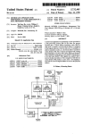
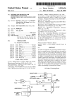
_
US005376819A
UllltGd States Patent [19]
[11] Patent Number:
Gay et al.
[45]
[54] INTEGRATED CIRCUIT HAVING AN ON
CHIP THERMAL CIRCUIT REQUIRING
ONLY ONE DEDICATED INTEGRATED
CIRCUIT PINAND METHOD OF
OPERATION
_
Date of Patent:
5,376,819
Dec. 27, 1994
OTHER PUBLICATIONS
MC8811O Second Generation RISC Microprocessor
User’s Manual, Motorola, Inc., Dec. 1991, pp. l1—6,
11-8, 11-17.
[75] Inventors: James G. Gay, P?ugerville; William
#- Ledbetter’ Jr” Austm’ both of
Fri-man, Examiner__Ngan V_ Ngo
Attorney, Agent, or Firm-Robert L. King
ex.
[73] Assignee: Motorola, Inc., Schaumburg, Ill.
[21] Appl NO. 158 323
.
..
[22] Filed:
Nov. 29, 1993
_
"""""""""" " HOIL
. .................................. "257/777-338/22 R,
. .
ABSTRACT
An integrated circuit implements an on chip thermal
circuit (12) for measuring temperature of an operating
integrated circuit die (10) by requiring only one dedi
,
5
[57]
[58] Field of Search ..................... .. 257/467’, 776, 777338/22
cated integrated circuit pin (16). A second integrated
circuit pin (18) is utilized but is also connected directly
connected to other circuitry (14) on the integrated cip
em‘ and is used by the ether circuitry at the Same time
References Cited
that the integrated circuit die temperature is being mea
sured. In one form, the second integrated circuit pin is
a ground terminal. Error voltages coupled to the
US. PATENT DOCUMENTS
ground terminal may be removed from the temperature
[56]
5,140,394
8/1992 Cobb, 111 et a1. ................. .. 257/467
5,l4l,334
8/1992
Castles
... ... ... .. .. ..
. . . ..
calculatmn by an external ‘ilfferem‘al “Pm-13(24)
257/467
5,230,564 7/1993 Bartilson et a1. .................. .. 257/467
14 Claims, 1 Drawing Sheet
V00
DIFFERENTIAL
FUNCTIONAL
AMPLIFIER F’VOUT
OPERATING
CIRCUIT
15
GND
1
5,376,819
2
SUMMARY OF THE INVENTION
INTEGRATED CIRCUIT HAVING AN ON CHIP
THERMAL CIRCUIT REQUIRING ONLY ONE
DEDICATED INTEGRATED CIRCUIT PIN AND
METHOD OF OPERATION
In accordance with one form of the invention, there is
provided an integrated circuit having an on chip ther
mal circuit requiring only one dedicated integrated
circuit pin and a method of implementing a single pin on
FIELD OF THE INVENTION
chip thermal circuit in an integrated circuit. The inte
grated
circuit comprises a die and a ?rst integrated
The present invention generally relates to integrated
circuit
pin
which is dedicated solely for use with the on
circuits, and more particularly, to the monitoring of
10 chip thermal circuit. A second integrated circuit pin is
thermal characteristics of an operating integrated cir
also provided. An integrated circuit die thermal sensing
cuit.
circuit is located on the die and directly connected to
the ?rst integrated circuit pin and to the second inte
BACKGROUND OF THE INVENTION
grated circuit pin. The integrated circuit die thermal
An important operating characteristic of an inte
sensing circuit comprises a material which has a physi
grated circuit is the temperature of the integrated cir
cal characteristic which varies in a manner proportional
cuit’s die when the integrated circuit is fully powered
to variation of temperature of the material. A functional
and in a normal operating mode of operation. Such a
operating circuit is located on the die and is connected
temperature measurement is often desired at a ?nal
directly to the second integrated circuit pin. The func
tional operating circuit performs a predetermined oper
ating function within the integrated circuit at the same
time the integrated circuit die thermal sensing circuit
provides an output signal which indicates an operating
package test when the integrated circuit is in the same
form as will be used by an end user. To satisfy this need,
others have used an on-chip resistor connected to two
dedicated external pins of the integrated circuit. The
external pins have no other function than to implement
the temperature measurement function. An example of
temperature of the die. The second integrated circuit
pin is used by both the integrated circuit die thermal
an integrated circuit having two dedicated .pins for
temperature measurement of the integrated circuit die is
the MC88110 reduced instruction set microprocessor.
The temperature of the integrated circuit having an
sensing circuit and the functional operating circuit.
These and other features, and advantages, will be
more clearly understood from the following detailed
description taken in conjunction with the accompany
ing drawings. It is important to point out that there may
on-chip resistor is measured by using a current source
reference and forcing a known current thru the known
resistance of the on-chip resistor. A resulting voltage
across the two dedicated integrated circuit pins is then
measured. The resulting voltage is proportional to the
temperature of the operating integrated circuit. In other
words, as the temperature of the operating integrated
circuit die varies, the resistance varies proportionately
which results in a proportional change in voltage mea
sured across the two dedicated integrated circuit pins.
The two dedicated integrated circuit pins are required
in order to isolate internally generated noise and other
circuit parameters from the two integrated circuit pins.
be other embodiments of the present invention which
are not speci?cally illustrated.
BRIEF DESCRIPTION OF THE DRAWINGS
35
FIG. 1 illustrates in block diagram form an on-chip
die thermal sensing circuit in accordance with the pres
ent invention; and
FIG. 2 illustrates in partial schematic form the differ
ential ampli?er of FIG. 1.
DETAILED DESCRIPTION OF A PREFERRED
EMBODIMENT
Illustrated in FIG. 1 is an integrated circuit die 10 in
Any voltage, current, resistance or impedance which is
coupled to the two integrated circuit pins from internal
accordance with the present invention. Although not
to the integrated circuit will modify the voltage poten 45 fully illustrated as a packaged integrated circuit for
tial between the two integrated circuit pins and result in
purposes of illustrating the present invention, integrated
an incorrect temperature measurement. However, the
price of two dedicated integrated circuit pins to imple
ment a measurement function is costly, even in the most
advanced very large scale integrated circuits.
Another type of integrated circuit which uses a plu
circuit die 10 should be considered as a fully encapsu
lated die in a completed integrated circuit chip. Inte
grated circuit die 10 generally has a die thermal sensing
circuit 12, a functional operating circuit 14, a ?rst inte
grated circuit pin 16, and a second integrated circuit pin
rality of resistors connected between the integrated
18. Also illustrated is a constant current source 20 and a
circuit’s external pins is a resistor network integrated
circuit. However, this type of integrated circuit func
differential ampli?er 24.
In the illustrated form, die thermal sensing circuit 12
tions only to provide a user with a plurality of possible
is implemented as a resistor having a ?rst terminal con
resistance values depending upon which pins of the
integrated circuit are connected. No other operating
circuitry is typically implemented in such circuits.
Yet another known type of integrated circuit which
nected to ?rst integrated circuit pin 16 and having a
second terminal connected to second integrated circuit
pin 18. In the illustrated form, the second integrated
circuit pin 18 is a ground reference pin of integrated
circuit die 10. Functional operating circuit 14 has a
terminal connected directly to the second integrated
provides a signal from which an operating die tempera
ture may be derived utilizes a signi?cant amount of
dedicated internal circuitry, such as an analog-to-digital
(A/D) circuit and a storage register, to provide the
circuit pin 18, thereby making the second integrated
circuit pin a common integrated circuit pin which is
signal at a single dedicated output pin of the integrated
common to both the die thermal sensing circuit 12 and
circuit. The additional internal circuitry which is re 65 the functional operating circuit 14. A constant current
quired to implement this temperature measurement
function is often prohibitive in many large scale integra
tion designs.
source 20 has a ?rst terminal connected to a power
supply voltage, such as VDD, and has a second terminal
connected to both the ?rst integrated circuit pin 16 and
5,376,819
3
a ?rst input of differential ampli?er 24. A second input
of differential ampli?er 24 is connected to the second
integrated circuit pin 18. An output of differential am
pli?er 24 provides an output voltage, Vout, which is
4
The present invention however can still be utilized
even when ground bounce errors exist. The voltage
variation across the resistance of die thermal sensing
circuit 12 attributable to ground bounce is common
referenced to a ground reference terminal and is pro
mode with respect to the ground bounce voltage varia
portional to temperature.
In operation, an operating temperature of integrated
tion at the common or second integrated circuit pin 18.
circuit die 10 may be accurately measured while circuit
bounce error which occurs across die thermal sensing
die 10 is fully operational. Further, this function only
requires one dedicated integrated circuit pin, the ?rst
integrated circuit pin because the second integrated
circuit pin is used concurrently by the functional oper
ating circuit 14. Functional operating circuit 14 per
circuit 12 is common mode makes it possible to elimi
nate the ground bounce error and thereby use only one
Recognizing that the voltage variation due to ground
dedicated integrated circuit pin for the die thermal
sensing. Differential ampli?er 24 may be used to sub
tract the common mode ground bounce noise from the
forms a predetermined operating function within the
output voltage between integrated circuit pins 16 and
integrated circuit 10 at the same time the present inven 15 18. Differential ampli?er 24 therefore recovers a pure
voltage which is proportional to the resistance of die
tion is utilized to determine the die operating tempera
ture. Examples of the functionality of operating circuit
thermal sensing circuit 12. In other words, differential
14 might include an execution unit, digital logic cir
ampli?er 24 removes a common mode error component
cuitry, address translation circuitry, a memory, etc.. In
one form, the die thermal sensing circuit 12 is imple
from a voltage differential between the ?rst and second
integrated circuit pins. Although two integrated circuit
mented as a resistor. If a metal resistor is utilized, a
pins are utilized, it should be noted that the common or
second integrated circuit pin 18 is already present on the
resistor may be formed which is susceptible to average
integrated circuit and is never taken out of operational
temperature changes of the integrated circuit die 10 and
use during the die thermal measuring process.
which provides a temperature coefficient of approxi
mately 1.2 Ohms/degree Centigrade. It should be well 25 Illustrated in FIG. 2 is a detailed diagram of one form
of a differential ampli?er which may be used as differen
understood that other materials, such as polysilicon for
tial ampli?er 24 in connection with constant current
example, may be used to implement die thermal sensing
circuit 12. As constant current source 20 provides a
constant reference current to integrated circuit die 10, a
source 20 and integrated circuit die 10. Elements in
FIG. 2 which are the same as elements in FIG. 1 are
small predetermined voltage is developed across the 30 identically numbered for clari?cation. Differential am
pli?er 24 has a ?rst operational ampli?er 31 having a
resistance of die thermal sensing circuit 12. The resis
?rst, noninverting (positive) input connected to inte
tance of die thermal sensing circuit 12 is proportional to
grated circuit pin 16. As was illustrated in FIG. 1, con
the temperature of the die in accordance with the fol
lowing equation:
stant current source 20 has the ?rst terminal thereof
35 connected to power supply voltage VDD and the second
Resistance of circuit 12=(Die Temp.) “ (Temp.
Coet'?cient)+K
'
(1)
where the die temperature is in units of degrees Centi
grade, the temperature coef?cient is in units of (Ohms/
degree Centigrade), and K is a minimum resistance in
Ohms which circuit 12 has. The temperature coef?cient
depends upon what material is selected as die thermal
terminal thereof connected to integrated circuit pin 16
of integrated circuit die 10. A second, inverting (nega
tive) input of operational ampli?er 31 is connected to an
output thereof and to a ?rst terminal of a resistor 33. A
second terminal of resistor 33 is connected to a first
terminal of a resistor 35. A second operational ampli?er
37 has a ?rst, noninverting (positive) input connected to
integrated circuit pin 18 which is a ground terminal on
sensing circuit 12, but is conventionally known for a
the integrated circuit package and therefore connected
given temperature range. As the die temperature 45 to ground. A second, inverting (negative) input of oper
changes, so does the resistance of die thermal sensing
ational ampli?er 31 is connected to an output thereof
circuit 12. An increase in die temperature causes an
and to a ?rst terminal of a resistor 39. A second terminal
increase in the resistance of die thermal sensing circuit
of resistor 39 is connected to a ?rst, noninverting (posi
12, and a decrease in die temperature causes a decrease
tive) input of a third operational ampli?er 41 and to a
in the resistance of die thermal sensing circuit 12. Since 50 ?rst terminal of a resistor 43. A second terminal of
the current through the resistance of die thermal sens
resistor 43 is connected to a ground reference terminal.
ing circuit 12 is constant, the voltage which is devel
A second, inverting (negative) input of operational
oped across the resistance of die thermal sensing circuit
ampli?er 41 is connected to both the second terminal of
12 is also proportional to the temperature of the die. In
resistor 33 and the ?rst terminal of resistor 35. A second
other words, when the die temperature increases the 55 terminal of resistor 35 is connected to an output of
voltage between the ?rst integrated circuit pin 16 and
the second integrated circuit pin 18 increases, and vice
versa.
In a highly integrated circuit, such as a data processor
for example, the amount of electrical current normally
channeled to or “sunk” by a ground terminal from the
functional operating circuit 14 can be substantial caus
operational ampli?er 41 and provides the output volt
age Vout. In one form, the three operational ampli?ers
may be obtained by using the commercially available
integrated circuit LF347 from National Semiconductor
Corporation which contains four operational ampli?ers.
A fourth operational ampli?er of an LF347 integrated
circuit may be used as the constant current source 20.
ing the ground potential to actually rise above zero
volts. Such an operating condition would therefore
In operation, operational ampli?ers 31 and 37 are
The error voltage is known in the art by the term
resistors 33, 35, 39 and 43 function to establish a gain of
differential ampli?er 24. For example, assume that resis
high impedance unity gain buffer stages which do not
create an error voltage between the ?rst integrated 65 load integrated circuit pins 16 and 18. Operational am
circuit pin v16 and the second integrated circuit pin 18.
pli?er 41 is con?gured as a differential ampli?er and
“ground bounce”.
5
5,376,819
6
tors 33 and 39 have the same resistance, R1, and assume
that resistors 35 and 43 have the same resistance R2.
noted that any type of circuitry, whether digital or
analog and regardless of process type, may be used as
Further assume that the output voltage of operational
ampli?er 31 is VR referenced to a ground potential, and
that the output voltage of operational ampli?er 37 is
VG referenced to the ground potential. The output volt
age Vout may therefore be represented as:
the functional circuitry which is connected to the com
V0ut= [(R2)/(R1)] ' [VG- VR]
(2)
where R1 is the resistance of each of resistors 33 and 39,
and R2 is the resistance of each of resistors 35 and 43.
As can be seen from equation 2, the ground bounce
noise is totally subtracted from the output voltage as a
result of the subtraction of VR from VG. In other words,
each of the VR and V6 voltages is referenced to ground,
and noise bounce which is injected into the ground is
therefore neutralized and invisible to the ?nal output
voltage provided by differential ampli?er 24.
mon integrated circuit pin 18. Another point which
should be noted is that the present invention may be
implemented by establishing a fixed voltage across the
die thermal sensing circuit 12 and measuring the current
thru die thermal sensing circuit 12 which is proportional
to die temperature. Although the present invention has
been disclosed in the context of a speci?c differential
ampli?er structure, other types of differential ampli?ers
may be used. Those skilled in the art will recognize that
modi?cations and variations can be made without de
parting from the spirit of the invention. Therefore, it is
intended that this invention encompass all such varia
tions and modi?cations as fall within the scope of the
appended claims.
We claim:
scores of circuit pins in which there is more than one
1. An integrated circuit having an on chip thermal
circuit requiring only one dedicated integrated circuit
ground reference terminal pin. Any ground reference
pin, the integrated circuit comprising:
It should be noted that many integrated circuits have
terminal may be used to implement the present inven
tion but it is preferable to connect differential ampli?er
24 to the same ground pin which the die thermal sensing
circuit 18 is connected to. If other ground pins are con
nected to differential ampli?er 24 than the ground pin
which die thermal sensing circuit 18 is connected to,
inductance and other electrical properties may create
differential voltage potentials between the various
ground circuit pins when the integrated circuit is opera
tional.
The present invention may alternately be used with
out the assistance of external differential ampli?er 24
and constant current source 20. For example, the resis
tance of die thermal sensing circuit 12 of integrated 35
a die;
a ?rst integrated circuit pin which is dedicated solely
for use with the on chip thermal circuit;
a second integrated circuit pin;
an integrated circuit die thermal sensing circuit lo
cated on the die and directly connected to the ?rst
integrated circuit pin and to the second integrated
circuit pin, the integrated circuit die thermal sens
ing circuit comprising a material which has a physi
cal characteristic which varies in a manner propor
tional to variation of temperature of the material;
and
a functional operating circuit also located on the die
and connected directly to the second integrated
circuit pin, the functional operating circuit per
forming a predetermined operating function within
circuit die 10 may be measured at room temperature
between integrated circuit pins 16 and 18 before the
integrated circuit is powered up. Then the integrated
the integrated circuit at the same time the inte
circuit may be powered up and is operational for a
grated circuit die thermal sensing circuit is provid=
ing an output signal which indicates an operating
temperature of the die;
suf?cient amount of time to allow the die to achieve a
characteristic operating die temperature. The power
should then be disconnected from the integrated circuit
and another resistance measurement of the die thermal
sensing circuit 12 immediately made. The differing re
sistance values can be used in accordance with equation 45
1 to provide an average operating temperature of the
integrated circuit. In this technique, ground bounce
noise does not exist and is therefore irrelevant.
Thus it is apparent that there has been provided, in
accordance with the present invention, an integrated
circuit having an on chip thermal circuit requiring only
one dedicated integrated circuit pin, and a method of
operating the unique integrated circuit. An advantage
of the present invention is the saving of an additional
dedicated integrated circuit pin to provide a die temper
ature when the die is powered up and operational. Al
though the invention has been described and illustrated
with reference to speci?c embodiments thereof, it is not
intended that the invention be limited to these illustra
tive embodiments. For example, one may utilize many
different types of die thermal sensing circuit 12 other
than a resistor. Further, pins other than the illustrated
ground pin which can function as the common inte
grated circuit pin 18 between the die thermal sensing
circuit 12 and other operating circuitry may be used. 65
For example, any ?xed voltage potential integrated
circuit pin may be used to implement the function of the
common integrated circuit pin 18. It should also be
said second integrated circuit pin being used by both
the integrated circuit die thermal sensing circuit
and the functional operating circuit.
2. The integrated circuit of claim 1 wherein the inte
grated circuit die thermal sensing circuit is a resistor.
3. The integrated circuit of claim 2 wherein the resis
tor is made of metal.
4. The integrated circuit of claim 1 wherein the sec
ond integrated circuit pin is a ?xed voltage potential
terminal.
5. The integrated circuit of claim 4 wherein the ?xed
voltage potential terminal is a ground reference termi
nal.
6. The integrated circuit of claim 4 further compris
ing:
circuitry external to the integrated circuit and con
nected to the ?rst and second integrated circuit
pins, the circuitry measuring a voltage potential
between the ?rst integrated circuit pin and the
second integrated circuit pin and removing any
common mode voltage component coupled to the
?xed voltage terminal to provide a voltage which
is proportional to the operating temperature of the
die.
7. A method of measuring an operating temperature
of an integrated circuit die of an integrated circuit re
7
5,376,819
sulting from the integrated circuit receiving electrical
power, comprising the steps of:
dedicating a single integrated circuit pin solely for
8
11. An integrated circuit having an on chip integrated
circuit die thermal circuit, the integrated circuit com
prising:
use with the method of measuring, the single inte
grated circuit pin used as a ?rst integrated circuit 5
pin to measure the temperature;
selecting a second integrated circuit pin to use with
the ?rst integrated circuit pin, the second inte
grated circuit pin being used additionally as a func
tional pin of the integrated circuit concurrent with
measuring the temperature;
directly connecting a thermal sensing circuit which is
integrated in the integrated circuit die to the ?rst
integrated circuit pin and to the second integrated
circuit pin, the integrated circuit die thermal sens 15
ing circuit comprising a material which has a physi
cal characteristic which varies in a manner propor
tional to variation of temperature of the material;
directly connecting a functional operating circuit
integrated in the integrated circuit die to the sec 20
ond integrated circuit pin, the functional operating
circuit performing a predetermined operating func
tion within the integrated circuit; and
concurrent with the functional operating circuit per
an integrated circuit die;
a ?rst integrated circuit pin which is dedicated solely
for use in measuring a temperature of the inte
grated circuit die when the integrated circuit is
receiving electrical power;
a second integrated circuit pin;
a thermal sensing circuit integrated in the integrated
circuit die, the thermal sensing circuit having a ?rst
terminal directly connected to the ?rst integrated
circuit pin and having a second terminal directly
connected to the second integrated circuit pin; and
circuitry connected directly to the second integrated
circuit pin, the circuitry being operational and
utilizing the second integrated circuit pin concur
rently while the ?rst and second integrated circuit
pins are used to provide a signal which is propor
tional to the temperature of the integrated circuit
die.
12. The integrated circuit of claim 11 wherein the
thermal sensing circuit is a resistor made of a material
consisting of one of: polysilicon and metal.
13. The integrated circuit of claim 11 further com
forming the predetermined operating function,
providing an output signal between the ?rst inte
grated circuit pin and the second integrated circuit
which is mathematically proportional to the oper
ating temperature of the die.
30
8. The method of claim 7 wherein the step of connect
ing an integrated circuit die thermal sensing circuit
further comprises:
prising:
a constant current source external to the integrated
circuit for providing a reference current to the ?rst
integrated circuit pin; and
a differential ampli?er external to the integrated cir
cuit and connected to the ?rst and second inte
grated circuit pins, the differential ampli?er remov
ing a common mode error component from a volt
connecting a resistor directly to the ?rst and second
age differential between the ?rst and second inte
integrated circuit pins.
grated circuit pins.
9. The method of claim 7 wherein the step of select
14. The integrated circuit of claim 11 further com
ing a second integrated circuit pin further comprises:
selecting a ?xed voltage potential pin of the inte
grated circuit as the second integrated circuit pin.
prising:
circuitry connected to the ?rst and second integrated
circuit pins, the circuitry removing a common
mode noise error from the signal which is propor
tional to the temperature of the integrated circuit
before translating the signal from an electrical
10. The method of claim 7 further comprising the step
of:
removing a common mode noise error from the out
put signal before translating the output signal from
value to a temperature value.
an electrical value to a temperature value.
*
45
50
55
65
*
*
*
Ii