1
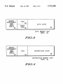
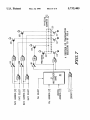
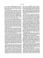
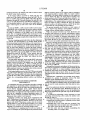
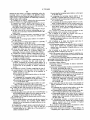
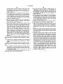
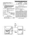
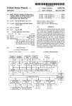
United States Patent [19]
[11] Patent Number:
Ho et al.
[45]
[54]
METHOD AND APPARATUS FOR
PERFORMING A CACHE OPERATION m A
DATA PROCESSING SYSTEM
5,732,405
Date of Patent:
Mar. 24, 1998
5,233,700 8/1993 Takagi ................................... .. 395/400
5,263,140 11/1993 Riordan ...... ..
395/417
5,412,787
5/1995 Iorsy? et a1. ......................... .. 3951417
[75] Inventors: Yui Kaye Ho, Austin; William C.
OTHER PUBLICATIONS
M033“, D?PPmg Sprmgs; Joseph A‘
Motorola MC88200 Cache/Memory Management Unit
Gutlel'rez’ Austm’ all of Tcx-
User’s Manual; 1989,1990; pp.
[73] Assignee: Motorola, Inc., Schaumburg, 111.
through viii, 1-1 through
343'
Primary Examiner—Eddie P. Chan
[21] APPL N03 336,702
Assistant Examiner—Hiep T. Nguyen
[22] Filed:
Attomey, Agent, or Fzrm—Susan C. Hill
Nov. 8, 1994
_
_
[57]
ABSTRACT
Related US. Application Data
[63]
6
[2:12]
[
1
A method and apparatus for performing a cache operation in
a data processing system (10). In one form, the present
Continuation of Ser. No. 955,818, Oct. 2, 1992, abandoned.
>
invention has a “block address translation cache (BATC)
.................................................
f '
' """""""""""" "
only mode” in which a reccivad logical address is Compared
'
’
to the logical addresses stored in only one of a plurality of
Fleld of Search ................................. "I.
address translation caches’ is. the block addt?ss 'Ianslation
395/413, 416, 418, 419, 365/49, 711/3,
cache (BATC) (76). The overhead associated with loading
206, 207, 208, 209
and comparing One or more other caches (78) is not incurred.
If the comparison with that one cache (BATC) (76) produces
a hit, that cache (BATC) (76) supplies the address that is
used as the physical address. If the comparison with that one
.
References Clted
Us PATENT DOCUMENTS
[56]
4,538,241
3951417
cache (BATC) (76) produces a miss, then a 1:1 mapping is
4,965,720 1011990 Mitchell et a1‘
8/1985 L _
t al
395,400
taicslejtriezigd the received loglcal address is used as the physical
5,107,417
4/1992 Yokoyama ......... ..
395/500
5,155,825 10/1992 Moughanni et al. .
395/425
CVlll e
5,230,045
.
.......................... --
‘
'
‘
7/1993 Sindhu .................................. .. 395/425
21 Claims, 6 Drawing Sheets
536429;;
TRANSLATION
FILE
ENABLE
Q
CONTROL REGISZZER
LOGICAL
ADDRESS
/ (TE)
"'"
MMU
l
vENABLE/DISABLE
(MEN)
BLOCK
ADDRESS
TRANSLATION
PAGE
ADDRESS
TRANSLATION
CACHE ‘(BATC)
E
CACHE (PATC)
E
BATC
,2
PAL
ADDRESS
LOGICAL
ADDRESS
HIT/MISS
BATC
ADDRESS
CACHE
RETRY
SELECT
LOGIC
PATC
ADDRESS
3,
m (IDENTITY) *
TRANSLATION
BATE SELECT
SELECTOR
‘ PATC SELECT
E
PAL SELECT
PHYSICAL
A PORTION OF- [EMORY MANAGEMENT
ADDRESS
LATCH (PAL)
UNIT (THU) 54 0F >F1G.2.
LIKEIISE, A PORTION OF MEMORY
E
MANAGEMENT UNIT ' (I110) 62
PHYSICAL
ADDRESS
'
'
‘
US. Patent
Mar. 24, 1998
Sheet 2 0f 6
5,732,405
‘MEMORY
MANG§§¥ENT
(MW)
TAGS 56
---- ---- --
FIG454
DATA CACHE
SNOOP
TAGS
g9
DATA MEMORY UNIT
(DMU) 5i
FIG-.2
MEMORY
MANAGEMENT
UNIT
(MMU)
-
TAGS
INSTRUCTION CACHE
F1014.
'62
Q5
IQ
INSTRUCTION MEMORY UNIT
(IMU) .42
FIG. 3
US. Patent
Mar. 24, 1993
Sheet 3 of 6
5,732,405
gggfgg;
TRANSLATION
FILE
ENABLE
Q
KUE)
CONTROL REGISTER
82
LOGICAL
ADDRESS
-"
MMU
ENABLE/DISABLE
"
BLOCK
(MEN)
\
‘
ADDRESS
TRANSLATION
TRANSLATION
CACHE (BATC)
Z2
-_
CACHE (PATC)
'7_8
2
I,
LOGICAL
ADDRESS
U
1!
_
RETRY
PAGE
ADDRESS
- PAL
ADDRESS
CACHE
HIT/MISS_
BATC
ADDRESS
V
SELECT
LOGIC
PATC
ADDRESS
V
V
I"
72
—
3’
, 1:1 (IDENTITY) '
TRANSLATION
BATC SELECT
SELECTOR
PATC SELECT
FIG-7
22v
7 PAL SELECT
PHYSICAL
A PORTION OF MEMORY MANAGEMENT
ADDRESS
LATCH (PAL)
UNIT (mm) .54 OF -FIG.2.
LIKETTISE, A PORTION OF MEMORY
Z5
-
MANAGEMENT UNIT‘QLHU) 62 0F FIG.3.
PHYSICAL.
ADDRESS
FIG.4L
US. Patent
Mar. 24, 1998
START
1
Sheet 5 0f 6
5,732,405
MMU (MEMORY MANAGEMENT UNIT)
C)
®—>v
_
BATG (BLOCK ADDRESS TRANSLATION CACHE)
PATC (PAGE ADDRESS TRANSLATION CACHE)
PA (PHYSICAL ADDRESS)
IS MMU
N0
.
ENABLED
(MEN=1?)
,
\84
Y)
1:1 (IDENTITY)
MAPPING
PA=LOGICAL
ADDRESS
86
'
‘
ATTRIDuTES FROM
CONTROL REGISTER
YES
DID I
‘
'
BATC
N0 89 (b
HIT?
"
87 .
1=1 (IDENTITY)
88
YES
' MAPPING
PA=DATG
PA=L0GIGAL
ADDRESS
_
DID
BATC HIT?
No
91
93
PATC HIT?
'
PA=BATC
ADDRESS
v
é
ATTRIBUTES
ATTRIBUTES FROM
FROM BATC
CONTROL REGISTER
- N0
(-97
v
YES
ATTRIBUTES
FROM BATC »
I ADDRESS
95
'
PA FROM
I TABLE SEARCH
ATTRIBUTES FROM
TABLE SEARCH
PA=PATC
ADDRESS
ATTRIBUTES
FROM PATC
FIG. 6 I (b
,
US. Patent
Mar. 24, 1998
Sheet 6 of 6
4382.5
@
m2.
Am
mm“
@J
h
0
o
T
m
l
2
i
m
w
5
HE
T
I
!
%
E$05:02 E5%?8.3
gT-HV-lml
v n.
2
mm:
mm
k AMA
@Jl,
E85 2
f. .
A?
5,732,405
mo<z m
W2
,
lw
.- .
“motaenumg.?,
HkUNRN
5,732,405
1
2
METHOD AND APPARATUS FOR
PERFORMING A CACHE OPERATION IN A
DATA PROCESSING SYSTEM
When the ATC does not contain the requisite logical-to
physical mapping, a translation “miss” (also called “no
This application is a continuation of prior application
Ser. No. 07/955,818, ?led Oct. 2, 1992, now abandoned.
cache in order to determine the physical address that corre
sponds to the received logical address. This search is often
match”) occurs, and a hardware state machine or a software
routine is invoked to search memory more distant than the
called a “table search” or a “table walk’ because it may
require the data processing system to access and read more
FIELD OF THE INVENTION
than one table stored in more distant memory.
The present invention relates in general to a data process
ing system, and more particularly to a method and apparatus
for performing a cache operation in a data processing
The advantage of the address translation cache (ATC) is
that it saves a great deal of time. Rather than having to
access tables in distant memory every time a translation is
system.
hardware addresses used by the semiconductor chips and
required, the data processing system can quickly access the
address translation cache and retrieve the correct physical
address for certain selected logical addresses.
A cache/memory management unit on the MC88200,
available from Motorola, Inc. of Austin, Tex., has a separate
memory unit for instructions and a separate memory unit for
data. Each of the two memory units (instruction and data)
has address translation logic containing a page address
translation cache (PATC) and a separate block address
electronic circuitry running the software.
translation cache (BAT C).
BACKGROUND OF THE INVENTION
Today’s high performance data processing systems rely
15
upon sophisticated memory management systems to trans
late logical addresses into real (physical) addresses. Logical
addresses are the software addresses used by the program
mer when writing software. Physical addresses are the
In a very simple microprocessor-based system, the central
processing unit (CPU) is linked directly to memory. With
this type of con?guration, no memory mapping or task
protection capabilities are provided, and the addresses gen
erated by the CPU directly identify the physical locations to
be accessed. This type of system, however, is unsuitable for
multiple-task operations since there is no protection to
prevent corruption of one task by another.
In the prior art MC88200, there are three available trans
25
A memory unit with one or more address translation
caches (ATCs) is often used to provide the address mapping
and the task protection needed to construct a multitasking
data processing system. The memory unit acts as an inter
face between the CPU and the physical memory. The
memory unit controls all accesses to physical devices, and
tasks can be prevented from accessing the resources owned
by other tasks. When under the control of an operating
system with virtual memory capabilities, the logical—to
physical mapping functions allow tasks to utilize the entire
address space of the CPU without detailed knowledge of the
physical characteristics of the system.
The logical address is generated by the CPU and received
lation modes: identity mode, PATC only mode, and both
PATC and BATC mode. First, in the identity mode, neither
the PATC nor the BATC is searched for a match; the physical
address is the same as the logical address. Second, in the
PATC only mode, both the PKI‘C and the BATC are searched
for a match in order to determine the corresponding physical
address. In the PAI‘ C only mode, the search of the BATC is
wasted overhead and the user must load the BATC with
values that will ensure that the BATC does not erroneously
cause a hit.
Third, in the both PATC and BATC mode, both the PATC
35 and the BATC are searched for a match in order to determine
the corresponding physical address. The MC88200 has no
mode in which only the BAT C is searched. Note that if both
the PATC and the BATC miss, a time consuming table search
operation must be performed in order to determine the
40
physical address that corresponds to the received logical
address.
The BATC provides logical-to-physical address transla
tion for 512K-byte blocks of memory. Normally these
blocks contain the operating system kernel or other high-use
software. Since these blocks are high-use blocks, caching
as an input by the memory unit. The memory unit, using one
or more address translation caches, performs address trans
lation and privilege checking for the logical address and, if
the mapping is valid, drives the corresponding physical
address to the data or instruction cache. Note that the
address translation at the block level provides faster data
cache access while avoiding ATC misses and their associ
ated table searches. The PATC, on the other hand, provides
corresponding physical address produced by an ATC may be
logical-to-physical address translation for smaller 4K-byte
'
used to access either data or an instruction, depending upon 50 pages of memory.
Whether the ATC is part of a data memory unit or part of an
Some data processing system applications require large
instruction memory unit
linear arrays of data. For example, a frame buffer for a color
Generally, a memory unit contains one or more address
translation caches which are used to perform address trans
lation and privilege checking; and the memory unit also
contains one or more caches which store actual data or
instructions. Each entry in the address translation cache
usually contains a logical address, a corresponding physical
address, and one or more protection or control bits
(collectively called attribute bits or attributes).
On each memory access, an incoming logical address is
55
monitor may consist of a large linear array of data which
corresponds to the pixels on the screen of the monitor. Such
a frame bu?er may be too large to use pages effectively. For
example, a frame buffer for a particular color monitor may
require as much as 4M-bytes of memory. Such a frame
buffer would require one thousand pages if each page was
4K-bytes. As a result, pages would not be an effective way
to handle this large of a frame buffer.
received by the memory unit and is compared to the logical
address portion of each entry in the appropriate ATC in order
to locate the requisite logical-to-physical mapping. When
In addition, it is usually desirable for the software routines
that operate on the frame buffers to be independent of the
application’s hardware con?guration. As an example, a
software routine which is used to modify a frame butfer is
the ATC contains the requisite logical-to-physical mapping,
65 usually written so that the same software routine can be used
a translation “hit” (also called a “match”) occurs, and the
AT C produces the corresponding physical address.
in applications having different memory sizes and/or moni
tor types.
5,732,405
3
4
Thus for some applications, blocks are the most e?icient
way to handle large linear arrays of data such as frame
BATC only mode was then incorporated into a new
approach to address translation which allowed more ?ex
butters. In the prior art MC88200, the both PATC and BATC
ibility to the system designer.
translation mode was the mode which was normally used to
The new BATC only mode eliminates the extra overhead
handle large frame butfers. Unfortunately. the both PATC
and BATC mode requires the extra overhead of loading and
checking the PA'I‘C even though only the BALI‘C is required.
Thus the software is required to properly load the PATC so
required for loading and checking the PATC 78 when only
the BATC 76 is being used for address translation. Note that
in the prior art PATC only mode. the unnecessary overhead
to load and check the BATC 76 was still required.
In addition, in the new BATC only mode, a BATC miss
that an erroneous hit does not occur. In addition, the hard
ware performs an unnecessary check by comparing the
incoming logical address to each entry in the PKI‘C.
10 defaults to a 1:1 mapping which is the same as the 1:1
mapping in identity mode. In 1:1 mapping. the physical
address is the same as the logical address. The default to 1:1
SUMMARY OF THE INVENTION
The previously mentioned needs are ful?lled and other
advantages achieved with the present invention. In one form,
the present invention is a method and apparatus for per
forming a cache operation in a data processing system
having a ?rst cache.
In one embodiment, the method includes the step of
mapping may be used in a variety of ways, thus allowing the
system designer to have more ?exibility.
15
20
receiving an incoming value as an input to the ?rst cache.
The method also includes the step of comparing the incom
ing value to a plurality of ?rst values stored in the ?rst cache.
In addition. the method includes the step of determining that
a ?rst cache miss has occurred if the incoming value does 25
not match any of the plurality of ?rst values stored in the ?rst
cache. And ?nally, the method includes the step of trans
mitting the incoming value as an output value if the ?rst
cache miss has occurred
The present invention will be understood by one skilled in
the art from the detailed description below in conjunction
The present invention can be used in a wide variety of
ways to improve the ef?ciency and ?exibility of data pro
cessing systems utilizing address translation.
DESCRIPTION OF THE FIGURES
BRIEF DESCRIPTION OF THE DRAWINGS
present invention;
FIG. 2 illustrates. in block diagram form, a data memory
unit 44 of FIG. 1 in accordance with one embodiment of the
present invention;
FIG. 3 illustrates, in block diagram form. an instruction
memory unit 42 of FIG. 1 in accordance with one embodi
require address translation with mapped address location
which do require address translation. The ?xed address
locations do not require an entry in the BATC 76. Thus, the
?xed address locations will always produce a BAT C miss
and will always default to 1:1 mapping in which the physical
address is the same as the logical address. The mapped
address locations. on the other hand, do require an entry in
the BATC 76. Thus, the mapped address locations will
always produce a BATC hit in order to determine the
corresponding physical address.
with the accompanying drawings.
FIG. 1 illustrates, in block diagram form. a data process
ing system 10 in accordance with one embodiment of the
For example, using the present invention the system
designer may interleave ?xed address locations which do not
35
FIG. 1 illustrates a data processing system 10. Integer
execution unit 12, integer execution unit 14, bit-?eld execu
tion unit 16, multiply execution unit 18, divide execution
unit 20, ?oating point add unit 22. pixel add execution unit
24, pixel pack execution unit 26, data unit 28, and register
?le 30 are all bi-directionally coupled to bus 34. In addition,
superscalar instruction unit 36 is coupled to bus 34 in order
to provide signals to bus 34.
Integer execution unit 12, integer execution unit 14,
bit-?eld execution unit 16, multiply execution unit 18,
divide execution unit 20, ?oating point add unit 22, pixel add
execution unit 24, and pixel pack execution unit 26, and data
ment of the present invention;
FIG. 4 illustrates, in block diagram form, a portion of 45 unit 28 are all coupled to bus 38 in order to receive signals
memory management unit (MMU) 54 of FIG. 2, which is
from bus 38. In addition, superscalar instruction unit 36 is
identical to a portion of memory management unit (MMU)
bi-directionally coupled to bus 38. Register ?le 30 is coupled
62 of FIG. 3, in accordance with one embodiment of the
to bus 38 in order to provide signals to bus 38.
present invention;
Target instruction cache 40 and instruction memory unit
FIG. 5 illustrates, in tabular form, four MMU address 50 (IMU) 42 are each bi-directionally coupled to superscalar
translation modes, how the modes are activated. the source
instruction unit 36. Data memory unit (DMU) 44 is
of attribute bits for each mode. and the mapping for each
bi-directionally coupled to data unit 28.
mode in accordance with one embodiment of the present
Instruction memory unit (IMU) 42 and data memory unit
invention;
(DMU)
44 are each bi-directionally coupled to bus interface
55
FIG. 6 illustrates, in ?ow chart form, a representation of
unit 46. Bus interface unit 46 has an external bus interface
the four MMU address translation modes; and
48 which is bi-directionally coupled to bus 50 and to bus 52.
In one embodiment of the present invention illustrated in
FIG. 7 illustrates. in partial block diagram form, partial
FIG. 1, all Of data processing system 10 is located on one
logic diagram form, and partial schematic diagram form. a
integrated circuit. and bus 50 and bus 52 are both external
portion of translation selector 70 of FIG. 4 in accordance
to data processing system 10.
with one embodiment of the present invention.
FIG. 2 illustrates a data memory unit (DMU) circuit 44 of
DESCRIPTION OF THE PREFERRED
FIG. 1. DMU 44 includes a memory management unit
EMBODIMENTS
(MMU) circuit 54, a tags circuit 56, a snoop tags circuit 58,
A more ef?cient and more ?exible approach to address 65 and a data cache circuit 60.
translation was needed. A BATC only mode was developed
in which only the BATC 76 is searched for a match. The
FIG. 3 illustrates an instruction memory unit (IMU)
circuit 42 of FIG. 1. IMU 42 includes a memory manage
5,732,405
5
6
meat unit (MMU) circuit 62, a tags circuit 64, and an
instruction cache circuit 68.
FIG. 4 illustrates a portion of memory management unit
(MMU) 54 of FIG. 2. Note that in one embodiment of the
control electrode coupled to a precharge signal. The second
present invention, the portion of MMU 54 which is illus
control electrode coupled to the output of NOR gate 94.
P-channel CMOS transistor 104, p-channel CMOS tran
sistor 106, and p-channel CMOS transistor 108 each have a
?rst current electrode coupled to the positive power supply
Voltage. Transistors 104, 106. and 108 each have a second
current electrode of transistor 100 is coupled to a ?rst current
electrode of an N-channel CMOS transistor 102. Transistor
102 has a second current electrode coupled to ground and a
trated in FIG. 4 is identical to a portion of memory man
agement unit (MMU) 62 of FIG. 3. In other embodiments of
the present invention. FIG. 4 may illustrate a portion of only
one memory management unit, or an identical portion of
10 current electrode which is coupled to the ?rst current elec
more than one memory management unit.
trode of transistor 102 at a node 110. A physical address [X]
value is output at node 110. N-channel CMOS transistor 112
Still referring to FIG. 4, a translation selector circuit 70
receives six control signals. three 1:1 (Identity) signals, a
BATC select signal, a PATC select signal, and a PAL select
signal, from a select logic circuit 72. Translation selector 70
and N-channel CMOS transistor 114 each has a ?rst current
electrode coupled node 110 and a second current electrode
then uses these six control signals to select which one of four
coupled to ground.
input address sources are used to produce the physical
address which is output by translation selector 70.
PATC address [X] is an input to NAND gate 116 and an
input to NOR gate 118. PAT C select signal is an input to
inverter 120 and an input to NOR gate 118. BATC address
[X] is an input to NAND gate 122 and an input to NOR gate
124. BATC select signal is an input to inverter 126 and an
input to NOR gate 124. The output of inverter 120 is an input
to NAND gate 116. The output of inverter 126 is an input to
NAND gate 122.
The output of NAND gate 116 is coupled to a control
electrode of transistor 106. The output of NAND gate 122 is
coupled to a control electrode of transistor 108. The output
of NAND gate 98 is coupled to a control electrode of
transistor 104. The output of NOR gate 118 is coupled to a
control electrode of transistor 112. The output of NOR gate
Translation selector 70_ receives a PAL address from
physical address latch (PAL) circuit 74. Physical address
latch (PAL) 74 receives as an input the physical address
which is produced by translation selector 70. Translation
selector 70. block address translation cache (BATC) logic
76. and page address translation cache (PATC) logic 78 each
receives a logical address as an input. BATC 76 produces a
BATC address which is input to translation selector 70.
PATC 78 produces a PATC address which is input to
translation selector 70. In one embodiment of the present
invention, BATC 76 produces two BATC hit/miss signals
which are input to select logic 72.
Control register ?le 80 has a control register 82. Control
register 82 has a translation enable bit (TE) and an MMU
enable/disable bit (MEN). In alternate embodiments of the
present invention, the TB bit and the MEN bit may be
located in the same register or in different registers. The TE
bit and the MEN bit are received by the select logic 72 as
inputs. Select logic 72 also receives a cache retry signal as
an input.
FIG. 5 illustrates, in tabular form, four MMU address
translation modes, how the modes are activated, the source
of attribute bits for each mode, and the mapping for each
124 is coupled to a control electrode of transistor 114.
OPERATION OF THE PREFERRED
EMBODIMENT
35
40
FIG. 6 illustrates, in ?ow chart form, a representation of
the four MMU address translation modes.
FIG. 7 illustrates a portion of translation selector circuit
70 of FIG. 4 in accordance with one embodiment of the
bits, translation selector 70 may include N circuits such as
the one illustrated in FIG.- 7. The “[X]” symbol indicated one
bit of a multi-bit address. For example, PATC address DI]
state will be a logic level one.
Referring to FIG. 1, data processing system 10 has two
memory units. DMU 44 which is used for data acquisition,
and IMU 42 which is used for instruction acquisition. Other
embodiments of the present invention may have only one
memory unit, may have multiple memory units, or may have
the functionality of multiple memory units combined into
mode in accordance with one embodiment of the present
invention.
present invention. The circuitry in FIG. 7 is used to perform
a 4:1 multiplexing operation for only one bit of address.
Thus the circuit in FIG. 7 produces only one bit of physical
address. In order to produce a physical address having N
The terms “assert” and “negate” will be used when
referring to the rendering of a signal, status bit. or similar
apparatus into its logically true or logically false state,
respectively. Ifthe logically true state is a logic level one, the
logically false state will be a logic level Zero. And if the
logically true state is a logic level zero, the logically false
one complex memory unit.
Referring to FIGS. 1 and 2, DMU 44 has a memory
50
management unit (MMU) 54 which receives logical
addresses and control signals from data unit 28. Referring to
FIGS. 1 and 3, IMU 42 has a memory management unit
(MMU) 62 which receives logical addresses and control
signals from superscalar instruction unit 36.
represents one bit of the multi-bit PATC address.
In one embodiment of the present invention, FIG. 4
55
illustrates a portion of memory management unit 54 which
Still referring to FIG. 7, a 2:1 multiplexer (MUX) 90
is identical to a portion of memory management unit 62.
receives the PAL select signal as a control input, and
Note that the control register ?le 80 may be located any
receives PAL address [X] and logical address [X] as data
where in data processing system 10, as long as the control
inputs. MUX 90 uses the PAL select signal to select which
register ?le 80 is coupled in some manner to select logic 72.
address bit to output. NOR gate 92 receives the three 1:1
In one embodiment of the present invention, the control
(Identity) signals as inputs. The output of NOR gate 92 is
register ?le 80 is located in register ?le 30 of FIG. 1.
coupled to an input of NOR gate 94 and to an input of
inverter 96. The output of inverter 96 is coupled to the input
In one embodiment of the present invention, the transla
of NAND gate 98. The output of MUX 90 is coupled to an
tion enable bit (TE) and the MMU enable/disable bit (MEN)
input of NOR gate 94 and to an input of NAND gate 98. 65 are used to help determine which address translation mode
is presently selected and being used. In alternate embodi
P-channel CMOS transistor 100 has a ?rst current elec
ments of the present invention, other control bits could be
trode coupled to a positive power supply voltage and a
5,732,405
7
8
used to help select which address translation mode is to be
used. In addition. in other embodiments of the present
invention, some of the address translations modes may
logical address is compared to the valid stored logical
addresses. In this embodiment of the present invention, a
cache hit will only occur when the following two conditions
are met: (1) the incoming logical address must match one of
perform dilferent operations than the address translation
the stored logical addresses; and (2) the incoming
supervisor/user bit must match the stored supervisor/user bit
modes described herein.
Select logic 72 receives four input signals and produces
which is associated with the stored logical address that
matched. In alternate embodiments of the present invention,
six output control signals as illustrated in FIG. 4. Using the
four input signals. select logic 72 determines which one of
no attribute bits or different attribute bits may be used as part
the six output control signals to assert. There are three 1:1
(identity) output control signals because there are three input
10
of the comparison step in determining whether or not there
is a cache hit.
conditions that may produce the same 1:1 mapping. Trans
lation selector 70 receives the six control signals from select
logic 72 and uses them to control a 4:1 multiplexing opera
Referring to the ?fth and sixth columns in FIG. 5. the
source of the attribute bits and the logical-to-physical
tion. Translation selector 70 receives four addresses, namely
PAL address. logical address, BATC address, and PAT C
address mapping varies depending upon the address trans
lation mode. For example, in identity mode, the mapping is
address. Translation selector 70 then selects one of these
four addresses to output as the physical address.
If one of the three 1:1 (identity) output control signals are
address) and a control register is used as the source of the
1:1 (i.e. the physical address is the same as the logical
attribute bits. The control register can be located anywhere
in data processing system 10, and in one embodiment of the
present invention, may be control register 82 in FIG. 4.
In BATC only mode there are two possible mappings
which may be used. depending upon whether or not there is
asserted. the physical address output from translation selec
tor 70 will be the same as the logical address received by
translation selector 70. If the BAT C select control signal is
asserted, the physical address output from translation selec
a BATC bit. If BATC 76 indicates a hit. that means that
tor 70 will be the same as the BATC address received by
BATC 76 contains the requisite logical-to-physical mapping.
translation selector 70. If the PATC select control signal is
asserted, the physical address output from translation selec
If BATC 76 indicates a hit. BATC 76 will also contain the
requisite attribute bits and BATC 76 will be the source of the
attribute bits. On the other hand, if BATC 76 indicates a
miss. that means that BATC 76 does not contain the requisite
tor 70 will be the same as the PATC address received by
translation selector 70. And if the PAL select control signal
is asserted. the physical address output from translation
logical-to-physical mapping. If BATC 76 indicates a miss,
the mapping is 1:1 (i.e. the physical address is the same as
the logical address) and a control register, for example
selector 70 will be the same as the PAL address received by
translation selector 70.
FIG. 5 illustrates characteristics of the-four MMU address
control register 82, is used as the source of the attribute bits.
translation modes used in one embodiment of the present
invention. The four address translations modes are listed in
the first column: identity mode. BATC only mode, PATC
only mode. and both PATC and BATC mode. The second
In PATC only mode, either PAT C 78 contains the requisite
logical-to-physical mapping and the attribute bits, or else a
35
table search operation to more distant memory must be
and third columns indicate the logic state of the translation
enable bit (TE) and the MU enable/disable bit (MEN) for
each of the four address translation modes.
The fourth column in FIG. 5 indicates whether a BATC
“hit” has occurred. A BATC hit occurs when an incoming
performed in order to retrieve the corresponding physical
logical address is compared with the valid logical addresses
stored in BATC 76. and the incoming logical address
distant memory must be performed in order to retrieve the
matches one of the valid logical addresses stored in BATC
76. A BATC miss occurs when an incoming logical address
address and attribute bits.
In both BATC and PATC mode, either BATC 76 or PATC
78 contains the requisite logical-to-physical mapping and
the attribute bits, or else a table search operation to more
corresponding physical address and attribute bits.
45
is compared with the valid logical addresses stored in BATC
76, and the incoming logical address does not match any of
the valid logical addresses stored in BAT C 76. A status bit,
called a valid bit. is associated with each stored logical
FIG. 6 illustrates, in ?ow chart form, a representation of
the four MMU address translation modes. If the MU
enable/disable bit (MEN) indicates that the MMU is
disabled, MEN=0 in the illustrated embodiment, then the
MMU will be in the identity mode and will follow the ?ow
illustrated by path 84. If the MEN bit indicates that the
address in BAT C 76. Each valid bit indicates whether or not 50 MMU is enabled, MEN=1 in the illustrated embodiment,
then the MMU will be in one of the other three modes and
its associated stored logical address is valid and thus should
be compared to an incoming logical address. Note that each
stored logical address in the PATC 78 also has an associated
valid bit.
The ?fth column in FIG. 5 illustrates the source of access 55
protection information. This access protection information is
collectively called attribute bits or attributes. The above
mentioned valid bit is an attribute bit. A supervisor/user bit
which is used to indicate whether the associated logical
PATC only mode or both BATC and PATC mode and will
follow the ?ow illustrated by path 87.
In the BATC only mode, following the ?ow illustrated by
address is in supervisor or user space is also an attribute bit.
In some embodiments of the present invention. attribute
bits may be used as part of the comparison step in deter
mining whether there is a cache hit or a cache miss. In some
embodiments of the present invention. each incoming logi
cal address has an associated incoming supervisor/user bit.
The incoming supervisor/user bit is compared to the stored
supervisor/user bits at the same time that the incoming
will follow the ?ow illustrated by path 85.
If the translation enable bit (TE) indicates that address
translation is not enabled, TE=0 in the illustrated
embodiment, then the MMU will be in the BATC only mode
and will follow the ?ow illustrated by path 86. If the TE bit
indicates that address translation is enabled, TE=1 in the
illustrated embodiment, then the MMU will be in either
65
path 86, there are two possible sources for the physical
address and for the attribute bits. If the logical address
received by BATC 76 matches one of the logical addresses
stored in BAT‘ C 76, i.e. there is a BAI‘C hit, then the. MMU
will follow the ?ow illustrated by path 88 and the physical
address will be retrieved from the BAT C entry which
5,732,405
10
address locations which do not require address translation
matched. Likewise, the attribute bits will be retrieved from
the BATC entry which matched.
If the logical address received by BATC 76 does not
match one of the logical addresses stored in BATC 76, i.e.
there is a BATC miss, then the MMU will follow the ?ow
with mapped address location which do require address
translations. The ?xed address locations do not require an
illustrated by path 89. The path illustrated by path 89 is the
same as the path illustrated by path 84. The mapping is 1:1
(i.e. the physical address is the same as the logical address)
and a control register is used as the source of the attribute
bits.
In prior art MMUs, a table search would be used in place
of path 89 in order to determine the physical address and the
attribute bits. Thus a BATC miss in BATC only mode causes
the MMU to perform as if the MMU was in the identity
10
cessing systems utilizing address translation.
While the present invention has been illustrated and
described with reference to speci?c embodiments, further
mode. This 1:1 mapping in BATC only mode may be used
modi?cations and improvements will occur to those skilled
in the art. For example, in alternate embodiments of the
present invention. any type of architecture for data process
ing system 10 may be used. The architecture illustrated in
FIG. 1 is just one possible architecture that may be used.
Likewise, alternate structures may be used for the portion
of MMU 54 and MMU 62 illustrated in FIG. 4. Although
FIG. 4 illustrates two address translation caches, BATC 76
and PATC 78, alternate embodiments of the present inven
in a variety of ways, thus allowing the system designer more
?exibility in designing an application using data processing
system 10.
The two remaining modes both follow the ?ow illustrated
by path 87. The determination as to whether BATC 76 has
hit or missed may be performed before, at the same time as,
or after the determination as to whether PATC 78 has hit or
missed. In some embodiments of the present invention, it
may be more time e?icient to perform the PATC hit/miss
determination and the BAT C hit/miss determination at the
same time. If BATC 76 has hit, then the MMU is in the both
BATC and PATC mode and the MMU will follow the ?ow
25
may use address translation caches which are divided along
boundaries other than memory blocks and memory pages.
Although the illustrated embodiment uses four MMU
address translation modes, as illustrated in FIG. 5, alternate
MMU is either in the both BATC and PATC mode or the
PATC only mode, and the MMU will follow the ?ow
The both BATC and PATC mode and the PATC only mode
are identical from path 93 to end point “A”. If the logical
address received by PPH'C 78 matches one of the logical
addresses stored in PATC 78, i.e. there is a PAT C hit, then
the MMU will follow the ?ow illustrated by path 95 and the
physical address will be retrieved from the PAT C entry
which matched. Likewise, the attribute bits will be retrieved
from the PATC entry which matched.
If the logical address received by PATC 78 does not match
one of the logical addresses stored in PATC 78, i.e. there is
a PATC miss, then the MMU will follow the flow illustrated
by path 97 and a table search operation will be required to
. embodiments of the present invention may use more or
fewer address translation modes. Alternate embodiments
may also de?ne the characteristics of some of the address
translation modes differently. The ?ow chart representation
35
Although the illustrated embodiment of the present inven
translation mode being used, alternate embodiments of the
present invention may use more, fewer, or no control bits.
Alternatively, the control bits may not be located in a control
register.
bits.
SUMlVIARY AND SOME ALTERNATE
EMBODIMENTS
In summation, the above speci?cation describes a method
and apparatus for performing address translation in a data
processing system 10. In one form, the present invention has
a new address translation mode, called “block address
55
only one of a plurality of address translation caches, i.e.
BAT C 76. The overhead associated with loading and com
paring any other caches is not incurred.
1. A method for performing a cache operation in a data
prising the steps of:
Referring to BATC only mode, if the comparison with
60
mapping as is produced by choosing identity mode.
65
ways. For example, the system designer may interleave ?xed
Although FIG. 7 illustrates one possible circuit imple
mentation of a portion of translation selector 70, other
alternate circuit implementations may be used.
Although the present invention has been illustrated in the
context of an address translation cache, the present invention
may be used for cache operations other than address trans
lation.
It is to be understood, therefore, that this invention is not
limited to the particular forms illustrated and that it is
intended in the appended claims to cover all modi?cations
that do not depart ?om the spirit and scope of this invention.
We claim:
processing system having a ?rst cache, the method com
BAI‘C 76 produces a hit, then BATC 76 supplies the address
that is used as the physical address. However, if the com
parison with BATC 76 produces a miss, then the received
logical address is used as the physical address. As a result,
a BATC miss in BAT C only mode produces the same 1:1
The default to 1:1 mapping may be used in a variety of
of the four MMU address translation modes illustrated in
FIG. 6 may be different.
tion used two control bits in a control register, namely the TB
bit and the MEN bit, to help determine which address
retrieve the corresponding physical address and attribute
translation cache (BATC) only mode”, in which a received
logical address is compared to the logical addresses stored in
tion may use any number of address translation caches.
Likewise, alternate embodiments of the present invention
illustrated by path 91. If BATC 76 has missed, then the
illustrated by path 93.
entry in BATC 76. Thus, the ?xed address locations will
always produce a BATC miss and will always default to 1: l
mapping in which the physical address is the same as the
logical address. The mapped address locations, on the other
hand, do require an entry in BATC 76. Thus, the mapped
address locations will always produce a BATC hit in order
to determine the corresponding physical address.
The present invention can be used in a wide variety of
ways to improve the ei?ciency and ?exibility of data pro
receiving an incoming value as an input to the ?rst cache;
comparing the incoming value to a plurality of ?rst values
stored in the ?rst cache;
determining that a ?rst cache miss has occurred if the
incoming value does not match any of the plurality of
?rst values stored in the ?rst cache; and
if the ?rst cache miss has occurred, transmitting the
incoming value as an output value,
5 ,732_.405
12
11
(i) receiving the incoming logical address as the input
wherein the ?rst cache is an address translation cache, the
to the ?rst cache;
incoming value is a logical address, the plurality of ?rst
values stored in the ?rst cache are logical addresses, and the
(ii) comparing the incoming logical address to the
plurality of logical addresses in the ?rst cache;
(iii) receiving the incoming logical address as an input
output value is a physical address for addressing a memory
Without further table walking.
2. A method as in claim 1, wherein the data processing
system is formed on a single integrated circuit.
3. A method as in claim 1. further comprising the step of:
determining that a ?rst cache hit has occurred if the
incoming value matches at least one of the plurality of
?rst values stored in the ?rst cache.
4. A method as in claim 3. further comprising the step of:
if the ?rst cache hit has occurred, transmitting one of a
plurality of second values stored in the ?rst cache as the
output value.
5. A method for performing address translation in a data
processing system having a ?rst cache. the method com
to a second cache;
(iv) comparing the incoming logical address to a plu
rality of logical addresses in the second cache; and
(v) determining whether a ?rst cache hit has occurred
10
based upon whether the incoming logical address
matches any of the plurality of logical addresses in
the ?rst cache.
13. A method as in claim 12, wherein execution of said
step (ii) overlaps with execution of said step (iv).
15
14. A method as in claim 12, wherein said step of
performing further comprises the step of:
(vi) if the ?rst cache hit has occurred. outputting one of a
prising the steps of:
plurality of physical addresses stored in the ?rst cache
(A) receiving an incoming logical address as an input to
the ?rst cache;
as a physical address.
15. A method as in claim 14, wherein said step of
(B) comparing the incoming logical address to a plurality
of logical addresses in the ?rst cache;
performing further comprises the step of:
(F) regardless of whether the ?rst cache miss has
occurred. outputting the incoming logical address as
the physical address if the data processing system is in
the method comprising the steps of:
receiving a logical address;
determining which of a plurality of address translation
modes is selected;
(vii) determining whether a second cache hit has occrn'red
(C) determining that a ?rst cache miss has occurred if the
based upon whether the incoming logical address
incoming logical address does not match any of the
matches any of the plurality of logical addresses in the
plurality of logical addresses in the ?rst cache; and
25
second cache.
(D) if the ?rst cache miss has occurred, outputting the
16.
A method as in claim 15, wherein said step of
incoming logical address as a physical address for
performing further comprises the step of:
addressing a memory without further table walking.
(viii) if the second cache hit has occurred, outputting one
6. Amethod as in claim 5, further comprising the step of:
of a plurality of physical addresses stored in the second
(E) performing steps (A). (B). (C). and (D) of claim 5 if
cache as a physical address.
the data processing system is in a ?rst one of a plurality
17. A method for performing address translation in a data
of address translation modes.
processing system having a ?rst cache and a second cache,
7. A method as in claim 6. further comprising the step of:
35
a second one of the plurality of address translation
modes.
8. A method as in claim 7, further comprising the step of:
if a ?rst mode of the plurality of address translation modes
is selected, performing the steps of:
(a) comparing the received logical address to a plurality
(G) performing the following steps when the data pro
of logical addresses in the ?rst cache;
(b) determining that a miss has occurred if the received
logical address does not match any of the plurality of
logical addresses in the ?rst cache; and
(c) outputting the received logical address as a physical
address for addressing a memory without further
tablewalking if the ?rst cache indicates that a miss
has occurred; and
if any mode other than the ?rst mode of the plurality of
cessing system is in a third one of the plurality of
address translation modes:
(i) receiving the incoming logical address as the input
to the ?rst cache;
(ii) comparing the incoming logical address to the
plurality of logical addresses in the ?rst cache;
(iii) receiving the incoming logical address as an input
to a second cache; and
(iv) comparing the incoming logical address to a plu
rality of logical addresses in the second cache.
50
9. A method as in claim 8. wherein execution of said step
(ii) overlaps in time with execution of said step (iv).
10. Amethod as in claim 8, wherein said step (G) further
comprises the step of:
(v) indicating that a ?rst cache miss has occurred because
the incoming logical address does not match any of the
55
(c) determining whether a ?rst cache hit has occurred
based upon whether the incoming logical address
matches any of the plurality of logical addresses in
the ?rst cache; and
(d) determining whether a second cache hit has
occurred based upon whether the incoming logical
address matches any of the plurality of logical
addresses in the second cache.
plurality of logical addresses in the ?rst cache.
11. Amethod as in claim 10, wherein said step (G) further
comprises the step of:
(vi) determining whether a second cache hit has occurred
based upon whether the incoming logical address
matches any of the plurality of logical addresses in the
second cache.
12. Amethod as in claim 7, further comprising the step of:
(G) performing the following steps when the data pro
cessing system is in a third one of the plurality of
address translation modes:
address translation modes is selected, performing the
steps of:
(a) comparing the received logical address to the plu
rality of logical addresses in the ?rst cache;
(b) comparing the received logical address to the plu
rality of logical addresses in the second cache;
18. A circuit for performing address translation in a data
65
processing system, the circuit comprising:
a ?rst cache circuit for receiving a logical address, for
comparing the logical address to a ?rst plurality of
5,732,405
14
13
for outputting a ?rst cache address in response to the
a ?rst cache circuit for receiving a logical address, for
comparing the logical address to a ?rst plurality of
logical address matching one of the ?rst plurality of
logical addresses stored in said ?rst cache circuit, and
logical addresses stored in said ?rst cache circuit, and
for outputting a ?rst cache address in response to the
logical addresses;
logical address matching one of the ?rst plurality of
a second cache circuit for receiving the logical address,
for comparing the logical address to a second plurality
of logical addresses stored in said second cache circuit,
logical addresses;
and for outputting a second cache address in response
to the logical address matching one of the second
plurality of logical addresses;
10
control means for determining which one of a plurality of
address translation modes is selected, said control
means having a control value; and
a logic means, coupled to said ?rst cache circuit, to said
second cache circuit, and to said control means, said
plurality of logical addresses;
a storage circuit for storing a previous physical address;
a control register ?le for storing a control value;
a control circuit, coupled to said control register ?le, said
control circuit determining which one of a plurality of
address translation modes is selected in response to
logic means for receiving the logical address, the ?rst
cache address, and the second cache address, said logic
means for selecting, based upon the control value,
receiving the control value from said control register
?le;
which one of the logical address, the ?rst cache
a plurality of control signals, provided by said control
circuit, said plurality of control signals having a unique
address, and the second cache address to output as a
physical address for addressing a memory without
further tablewalking, said logic means outputting the
logical address as the physical address when both the
control value is a ?rst value and the logical address
does not match any of the ?rst plurality of logical
logic state for each of the plurality of address transla
tion modes; and
a translation selector circuit, coupled to said ?rst cache
circuit for receiving the ?rst cache address, coupled to
said second cache circuit for receiving the second cache
addresses.
19. The circuit for performing address translation in a data
processing system according to claim 18, further compris
mg:
a second cache circuit for receiving the logical address,
for comparing the logical address to a second plurality
of logical addresses stored in said second cache circuit,
and for outputting a second cache address in response
to the logical address matching one of the second
3O
address, coupled to said storage circuit for receiving the
previous physical address, and coupled to said control
circuit for receiving said plurality of control signals, in
response to receiving said plurality of control signals,
a processing unit, coupled to said ?rst and second cache
said translation selector circuit selecting which one of
circuits, said processing unit producing the logical
the logical address, the ?rst cache address, the second
cache address, and the previous physical address to
address.
20. The circuit for performing address translation in a data
processing system according to claim 19, further compris
ing:
a bus coupled to said processing unit, to said ?rst cache
circuit, and to said second cache circuit, said bus for
transferring the logical address to both said ?rst and
second cache circuits.
35
output as a current physical address, said translation
selector circuit outputting the logical address as the
current physical address for addressing a memory with
out further tablewalking when a ?rst one of said
plurality of address translation modes is selected and
the logical address does not match any of the ?rst
plurality of logical addresses.
21. A circuit for performing address translation in a data
processing system, the circuit comprising:
*
*
*
*
*