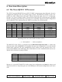
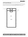
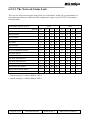
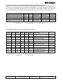
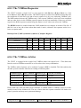
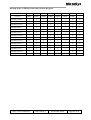
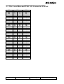
1
User’s Manual CPU87 Rev. 4 2nd edition Declaration of Conformity We, Manufacturer MicroSys Electronics GmbH Mühlweg 1 D-82054 Sauerlach Germany declare that the product CPU87 is in conformity with: EN 50081-1 Generic emission standard EN 50082-1 Generic immunity standard in accordance with 89/336 EEC-EMC Directive. We also declare the conformity of the above mentioned product with the actual required safety standards in accordance with Low Voltage Directive 73/23 EEC. Date: Signature: Position: General Manager The information in this document has been carefully checked and is believed to be entirely reliable. However, no responsibility is assumed for inaccuracies. Furthermore, MicroSys reserves the right to make changes to any product herein to improve reliability, function or design. MicroSys does not assume any responsibility arising out the application or use of any product or circuit described herein, neither does it convey any license under its patent rights or the rights of others. All rights reserved. MicroSys Electronics GmbH 2001. MicroSys Made for Professionals Edition Date: Ident-Nr.: Manual 10.06.2002 EW285MA-04AA 13.12.2007 EW285MA-04AB Schematics 17.02.2003 Datei: CPU874AB.DOC © 2000-2007 MicroSys Electronics GmbH Archivierung: 5 Released: EW285SL-04AA EW285MA-04AA Page 3 of 84 MicroSys Made for Professionals MicroSys GmbH, Mühlweg 1, 82054 Sauerlach, Germany. (ISDN) Hotline (08104) 801-130, Phone (08104) 801-0, Fax (08104) 801-110. Internet: http://www.MicroSys.de © MicroSys Electronics GmbH, December 2007 Page 4 of 84 EW285MA-04AB Archivierung: 5 Datei:CPU874AB.DOC © 2000-2007 MicroSys Electronics GmbH MicroSys Made for Professionals Table of Contents 1. Introduction ............................................................................................................................... 7 1.1 Short Description .............................................................................................................. 7 1.2 Specifications .................................................................................................................... 8 1.3 Related Documentation ..................................................................................................... 8 2. Delivery..................................................................................................................................... 9 2.1 Items shipped with this unit .............................................................................................. 9 2.2 Hints for unpacking, handling and storing ........................................................................ 9 3. Installation............................................................................................................................... 10 3.1 Items required for CPU87 installation ............................................................................ 10 3.2 Points to be observed ...................................................................................................... 10 4. Board Overview ...................................................................................................................... 11 4.1 Features CPU87............................................................................................................... 11 5. Address Map CPU87............................................................................................................... 13 5.1 The 603e-Bus Address Map ............................................................................................ 13 5.2 The I2C-Bus Address Map .............................................................................................. 14 6. Functional Description ............................................................................................................ 15 6.1 The PowerQUICC II Processor ....................................................................................... 15 6.1.1 The Debug Port ....................................................................................................... 16 6.1.2 The Processor Pin Configuration ............................................................................ 17 6.2 Memory ........................................................................................................................... 22 6.2.1 The SDRAM Area................................................................................................... 22 6.2.2 The Boot Socket ...................................................................................................... 23 6.2.2.1 Type Selection for Boot-ROM Socket ................................................................ 24 6.2.2.2 Socket Pin out: .................................................................................................... 25 6.2.2.3 Boot Options ....................................................................................................... 26 6.2.3 The Flash Memory .................................................................................................. 27 6.2.3.1 The FLASH Memory Write Protection............................................................... 28 6.2.3.2 Flash Address Map for 64 Bit Boot Option ........................................................ 29 6.2.4 The DiskOnChip Socket ....................................................................................... 30 6.2.4.1 Socket Pin out: .................................................................................................... 31 6.2.5 The Static RAM Area.............................................................................................. 32 6.2.5.1 Low-Battery Monitor........................................................................................... 32 6.2.5.2 The DPRAM Shared Address Decoding............................................................. 33 6.3 The I2C Bus ..................................................................................................................... 34 6.3.1 The EEPROM ......................................................................................................... 34 6.3.2 The Real Time Clock .............................................................................................. 34 6.3.2.1 The PCF8563T Address Map.............................................................................. 35 6.3.3 The System Hardware Monitor ............................................................................... 36 6.4 Miscellaneous.................................................................................................................. 37 6.4.1 The Backup Feature................................................................................................. 37 6.4.2 The Board Reset Function....................................................................................... 37 6.4.3 Hardware Watchdog Timer ..................................................................................... 38 6.4.4 Board Control Register............................................................................................ 39 Datei: CPU874AB.DOC © 2000-2007 MicroSys Electronics GmbH Archivierung: 5 EW285MA-04AA Page 5 of 84 MicroSys Made for Professionals 6.4.5 Board Revision Register ......................................................................................... 40 6.5 The CPU87 Interfaces ..................................................................................................... 41 6.5.1 The Serial I/Os ........................................................................................................ 41 6.5.2 The Fast Ethernet Ports ........................................................................................... 42 6.5.2.1 The 10/100Mbps LAN Interface Connector ST3-A ........................................... 43 6.5.2.2 The 10/100Mbps LAN Interface Connector ST3-B............................................ 43 6.5.2.3 The Network Status Leds .................................................................................... 44 6.6 The Floppy Disk Controller (Option) ............................................................................. 45 6.6.1.1 The Floppy Interface Connector ST2.................................................................. 46 6.7 Interrupt Structure ........................................................................................................... 47 6.7.1 The Interrupt Handler.............................................................................................. 47 6.7.2 The VMEbus Interrupt Handler .............................................................................. 47 6.7.2.1 The VMEbus Interrupt Acknowledge ................................................................. 49 6.7.3 The Onboard Interrupt Handler............................................................................... 50 6.8 The VMEbus Interface.................................................................................................... 53 6.8.1 Pin Assignment of the VMEbus Connector ST2 .................................................... 57 6.8.2 The VMEbus Mailbox ............................................................................................ 58 6.8.3 The VMEbus Requester .......................................................................................... 60 6.8.4 The VMEbus Arbiter .............................................................................................. 60 6.8.5 The VMEbus Timer ................................................................................................ 61 6.8.6 Preparations for VMEbus Multiprocessing............................................................. 61 7. Register Overview................................................................................................................... 62 8. Front Panel Description .......................................................................................................... 68 8.1 Front Leds ....................................................................................................................... 69 8.1.1.1 The User Programmable Leds............................................................................. 69 8.1.1.2 The Network Status Leds .................................................................................... 69 8.1.2 Front Switches......................................................................................................... 69 9. The Mezzanine Slot ................................................................................................................ 70 9.1 The Local Bus Module Slot ............................................................................................ 71 9.2 The Local Bus Connector Pin out ................................................................................... 71 9.3 The Local Bus and PMC I/O Connector Pin out............................................................. 72 9.4 The PMC Module Slot .................................................................................................... 73 9.5 The PMC PCI Connector Pin out.................................................................................... 74 10. The ispLSI Programming Port ............................................................................................ 75 11. Summary of Jumpers .......................................................................................................... 76 11.1 Jumpers Component Side ............................................................................................... 77 11.2 Jumpers Solder Side........................................................................................................ 78 Appendices...................................................................................................................... 79 Appendix A: I/O Connector Overview .................................................................... 80 Appendix B: Layout Component Side ..................................................................... 81 Appendix C: Layout Solder Side ............................................................................. 83 Appendix D: Schematics CPU87 (on request)......................................................... 84 Page 6 of 84 EW285MA-04AB Archivierung: 5 Datei:CPU874AB.DOC © 2000-2007 MicroSys Electronics GmbH MicroSys Made for Professionals 1. Introduction 1.1 Short Description The Double Euro sized board CPU87 is based on the Motorola PowerPC MPC8270. It features a 64 bit wide data bus for the 32 (64/128) Mbytes SDRAM area and the 8 Mbytes Flash memory bank. Additionally, it offers two 8 bit wide 32 pin JEDEC sockets for a boot ROM and a DiskOnChip device. An additional 16 bit wide SRAM area with battery backup is shareable with any other VMEbus master. The I2C-Interface of the MPC8270 controls a 2KBytes EEPROM, a RTC with battery backup and a System Monitor for supply voltage supervision. The CPM Module of the MPC8270 handles two 10/100Mbit Ethernet ports, three RS232 communication ports and two special RS422 and RS485 interfaces . The local bus of the MPC8270 is accessible via a 64 pin extension connector. A PMC slot is connected to the PCI interface, replacing the local bus lines. The VMEbus interface contains a single level arbiter, a requester with a four level ROR option and a 7 level interrupt handler. The short I/O decoded mailbox with interrupt capability allow for process synchronization. For background debug purposes the JTAG/COP interface of the MPC8270 is accessible via a 16 pin standard wrap connector. The complete board is implemented in CMOS technology, which allows for a power consumption as low as: 5V / 9W @ 450 MHz CPU speed. The 5 volt board supply voltage is protected by a transient suppresser diode against over voltage or wrong polarity. The CPU87 conforms to the VMEbus specification ANSI/IEEE STD1014-1987, IEC 821 & 297. Datei: CPU874AB.DOC © 2000-2007 MicroSys Electronics GmbH Archivierung: 5 EW285MA-04AA Page 7 of 84 MicroSys Made for Professionals 1.2 Specifications The power requirements for the CPU87 board are shown in the following table. Power Requirements: +5V, +5%/-2.5%, +12V, +5%/-2.5% -12V, +5%/-2.5% (t.b.d.) (typ. @450 MHz) for PMC slot only for PMC slot only Environmental Requirements: Operating Temperature Relative Humidity Storage Temperature 0 ° C to +70 ° C -40°C to +85°C optional 0 to 95 % (non-condensing) -40 ° C to + 85 ° C 1.3 Related Documentation The following manuals are applicable to the CPU87: − MPC8270 Power QUICC-II Microprocessor User’s Manual − HY57V651620B-TC7 4x1Mx16 SDRAM Data Sheet (Note: DRAM may actually vary, depending on the specific version and availability) − I28F160C3B Intel Boot Block Flash Memory Data Sheet (Note: Flash may actually vary, depending on the specific version and availability) − LM81 System Hardware Monitor Data Sheet − PCF8563 Real-Time-Clock User’s Manual − X24C164 EEPROM Data Sheet − DiskOnChip 2000 User’s Manual − VMEbus Specification Manual ANSI/IEEE STD1014-1987 Page 8 of 84 EW285MA-04AB Archivierung: 5 Datei:CPU874AB.DOC © 2000-2007 MicroSys Electronics GmbH MicroSys Made for Professionals 2. Delivery 2.1 Items shipped with this unit − User's Manual CPU87 Hardware − MicroSys shipping carton ATTENTION: STATIC DISCHARGE CAN DESTROY UNIT 2.2 Hints for unpacking, handling and storing − Avoid touching areas of integrated circuitry. − Unit should only be placed on a static-free conductive surface − Unit must only be transported using anti-static bags or MicroSys shipping carton − Packing should be saved if unit needs to be reshipped or returned − When the unit needs to be stored, it should be placed in a moist free, dust free environment. The storage temperatures and humidity specifications are shown in chapter 1 Datei: CPU874AB.DOC © 2000-2007 MicroSys Electronics GmbH Archivierung: 5 EW285MA-04AA Page 9 of 84 MicroSys Made for Professionals 3. Installation 3.1 Items required for CPU87 installation For installation of the CPU87, the following items are required. − Card cage or housing − VMEbus motherboard − Adequate rated power supply 3.2 Points to be observed Before the unit is inserted into the card cage, the following points should be observed. − Unit requires +5V (+ 5 %, - 2,5 %). − Unit requires +12V (+ 5 %, - 2,5 %) for PMC extension. − Unit requires -12V (+ 5 %, - 2,5 %) for PMC extension. − Be sure voltage is of correct polarity. − Check default jumper or switch setting. The card cage must be well ventilated. The operating temperature must never exceed its specified range. GUARANTEE IS VOID IF UNIT IS OPERATED OUT OF IT’S SPECIFICATIONS! Page 10 of 84 EW285MA-04AB Archivierung: 5 Datei:CPU874AB.DOC © 2000-2007 MicroSys Electronics GmbH MicroSys Made for Professionals 4. Board Overview 4.1 Features CPU87 Board Format: double euro card format Main Processor: MPC8270 with PowerPC 603e Core 64 Bit 603e-bus 32 Bit local bus 16 Kbytes instruction cache 16 Kbytes data cache up to 450 MHz CPU core clock rate CPM interface with four SCCs & one SMC Dynamic RAM: four SDRAM devices 32 Mbytes capacity (optional 64MB or 128MB) 64 bit data bus width Flash Memory: 8 Mbytes capacity 64 bit data bus width single 3.3 volt programmable devices Boot ROM Area: one 32 pin socket according to JEDEC standard max. 1 Mbytes capacity (512Kbytes for FLASH types) device type selection by soldering links 8 bit data bus width 5 volt supply ROM, PROM, EPROM, EEPROM, FLASH support Static DPRAM: 64 Kbytes (max. 1 Mbytes) SRAM capacity 16 bit data bus width data backup with onboard supply accessible by other VMEbus masters EEPROM: I2C serial access device 2KBytes capacity DiskOnChip: MD-2800-D08 5V device (optional) 32 pin socket with standard JEDEC pin out FD-Interface: FDC37C78 Floppy Disk Controller (optional) Real Time Clock: I2C serial access device PCF8563 with time & date function backup function with onboard supply Serial Interfaces: 2 SMCs with RS232 interface 2 SCCs with configurable buffers via I/O modules I2C serial access device LM81 hardware monitor for temperature and voltage control System Control: Data Backup: Datei: CPU874AB.DOC © 2000-2007 MicroSys Electronics GmbH short time backup via service free gold cap extended backup via 260mAh lithium cell (CR2430) external backup via VMEbus standby line Archivierung: 5 EW285MA-04AA Page 11 of 84 MicroSys Made for Professionals features CPU87 continued: Network Capabilities: two IEEE compliant Fast Ethernet PHY Transceivers full-duplex operation for 100BASE-TX and 10BASE-T Front Panel LEDs: four network status LEDs four user programmable LEDs Front Panel Keys: ABORT key with level 1 interrupt capability RESET key for complete hardware reset hardware watchdog timer with system reset programmable time out rate via external parts Watchdog: Debug Features: 16 pin JTAG/COP Interface Interrupt Handler: 7 level onboard interrupt handler 7 level VMEbus interrupt handler software programmable interrupt mask System Controller: full VMEbus slot 1 functions, single level arbiter single jumper function enable VMEbus Interface: according to ANSI/IEEE STD1014-1987 VMEbus Master: DTB A16/A24/A32 -D8/D16/D32 VMEbus address modifier support standard, extended and short I/O addressing dynamic bus sizing feature VMEbus Slave: DTB A24/A32 -D8/D16 programmable VMEbus access base address programmable VMEbus access window size DTB A16 -D8/D16 programmable VMEbus access base address VMEbus Mailbox: short I/O decoded with interrupt capability VMEbus Arbiter: single level arbiter on level 3 VMEbus Requester: single level 2:1 pass requester release when done or 4 level release on request modes Mezzanine Slot: PMC form factor Local Bus Interface for MPC8260 Processor type 3.3V PCI Interface for MPC8250 and MPC8270 Processor type Page 12 of 84 EW285MA-04AB Archivierung: 5 Datei:CPU874AB.DOC © 2000-2007 MicroSys Electronics GmbH MicroSys Made for Professionals 5. Address Map CPU87 5.1 The 603e-Bus Address Map Type Base End SDRAM Bank $0000 0000 Dual Ported SRAM Area $4000 0000 Bus Size $01FF FFFF CS2 603 64Bit $4001 FFFF CS3 603 16Bit CS4 603 8Bit DiskOnChip Socket $F400 0000 FDC37C78 Controller Std.Access $F100 0000 $F100 007F CS5 603 8Bit FDC37C78 Controller DMA Access $F100 0080 $F100 00FF CS5 603 8Bit VMEbus Ext.Address Compare Register $F200 0000 $F200 0000 CS6 603 8Bit VMEbus Std.Address Compare Register $F200 0001 $F200 0001 CS6 603 8Bit VMEbus Mb.Address Compare Register $F200 0002 $F200 0002 CS6 603 8Bit Board Control Register $F200 0003 $F200 0003 CS6 603 8Bit Board Status Register $F200 0004 $F200 0004 CS6 603 8Bit Watchdog Retrigger Port $F200 0005 $F200 0005 CS6 603 8Bit Clear Mailbox IRQ Port $F200 0006 $F200 0006 CS6 603 8Bit Revision Register $F200 0007 $F200 0007 CS6 603 8Bit VMEbus IRQ Mask Register $F200 0080 $F200 0080 CS6 603 8Bit VMEbus IRQ Status Register $F200 0081 $F200 0081 CS6 603 8Bit Local IRQ Mask Register $F200 0082 $F200 0082 CS6 603 8Bit Local IRQ Status Register $F200 0083 $F200 0083 CS6 603 8Bit PMC IRQ Status Register $F200 0084 $F200 0084 CS6 603 8Bit Power QUICC-II Internal Memory $F000 0000 --- 603 32Bit VMEbus Extended Access Range I $8000 0000 $80FF FFFF CS7 603 32Bit VMEbus Extended Access Range II not initialized not initialized CS11 603 32Bit VMEbus Standard Access Range $FE00 0000 $FEFF FFFF CS8 603 16Bit VMEbus Short I/O Access Range $FD00 0000 $FD07 FFFF CS9 603 16Bit VMEbus Int.Ackn. Access Range $FD08 0000 $FD0F FFFF CS9 603 16Bit Flash Memory Bank $FF00 0000 $FF7F FFFF CS1 603 64Bit 1 Boot ROM Socket $FFF0 0000 $FFFF FFFF CS0 603 8Bit 1 Boot ROM Socket $FF00 0000 $FF0F FFFF CS1 603 8Bit 2 64Bit 2 Flash Memory Bank 1 Select $FF80 0000 ) BTMD Jumpers set to 1-2 and 3-4 2 $FFFF FFFF CS0 603 ) BTMD Jumpers set to 1-3 and 2-4 Note! The address map shown above reflects the standard MicroSys initialization. Due to the flexibility of the MPC8270 memory controller, nearly any customized address map may be defined. Datei: CPU874AB.DOC © 2000-2007 MicroSys Electronics GmbH Archivierung: 5 EW285MA-04AA Page 13 of 84 ) ) ) ) MicroSys Made for Professionals 5.2 The I2C-Bus Address Map Type write read $B0..$BE $B1..$BF I2C-Bus LM81 System Hardware Monitor $58 $59 I2C-Bus PCF8563 Real Time Clock $A2 $A3 I2C-Bus 24C164 EEPROM Page 14 of 84 EW285MA-04AB Archivierung: 5 Datei:CPU874AB.DOC © 2000-2007 MicroSys Electronics GmbH MicroSys Made for Professionals 6. Functional Description 6.1 The PowerQUICC II Processor The CPU87 uses the MPC8270 Power QUICC-II RISC microprocessor from Motorola. It can be configured for different CPU core and bus speed versions. The MPC8270 contains a 603e compatible core with 16 Kbytes data cache and 16 Kbytes instruction cache. It uses a 3,3 volt bus supply and a 1,8 volts core supply voltage. The processor works with CPU clock rates up to 450 MHz and the according system clock rate varies from 50 to 100 MHz. The desired clock configuration can be adjusted via the soldering link area MDCK according to the following table. 1-2 X X X X --------- MDCK 3-4 X X ----X X ----- MPC8270 - 100/300/450 MHz System-Clock CPM-Clock CPU-Clock 33MHz 99MHz 132MHz 33MHz 99MHz 165MHz 33MHz 132MHz 132MHz 33MHz 132MHz 165MHz 100MHz 128MHz 450 MHz 1) 66MHz 132MHz 198MHz 66MHz 165MHz 165MHz 66MHz 165MHz 198MHz 5-6 X --X --X --X --1 ) Resulting clock rates with 50 MHz Oscillator (OSC1) ( x = link installed / --- link not installed ) The MPC8270 of the CPU87 is configured for the MPC8270-stand-alone-mode, i.e. not for the 603e bus mode. If the link RCFG is not installed, the power up configuration is set to the internal default mode. Otherwise the reset configuration word is taken out of the memory device connected to the CS0 line of the MPC8270. The 64 bit flash area or the 8 bit ROM socket can be configured as boot memory by jumper BTMD. BTMD Pin 1-2 Pin 3-4 Pin 1-3 Pin 2-4 Function CS0 connected to 8 bit socket CS1 connected to 64 bit Flash CS0 connected to 64 bit Flash CS1 connected to 8 bit socket RCFG closed --open or closed --- Because of a special BCTL0/BCTL1 buffer control, the configuration word must be always read from the boot device. Only during the use of the BDM port, the internal configuration word can be used. Datei: CPU874AB.DOC © 2000-2007 MicroSys Electronics GmbH Archivierung: 5 EW285MA-04AA Page 15 of 84 MicroSys Made for Professionals 6.1.1 The Debug Port The JTAG/COP interface of the CPU87 can be used via the 16 pin standard wrap connector JTAG according to following table. JTAG Signal Signal JTAG Pin 1 TDO GND Pin 2 Pin 3 TDI TRST# Pin 4 Pin 5 QREQ# 2K2 pullup Pin 6 Pin 7 TCK n.c. Pin 8 Pin 9 TMS n.c. Pin 10 Pin 11 SRST# GND Pin 12 Pin 13 HRST# n.c. Pin 14 Pin 15 CKSTPO# GND Pin 16 Page 16 of 84 EW285MA-04AB Archivierung: 5 Datei:CPU874AB.DOC © 2000-2007 MicroSys Electronics GmbH MicroSys Made for Professionals 6.1.2 The Processor Pin Configuration The MPC8270 offers a wide variety of pin functional swapping. The CPU87 uses the multi functional processor pins according to following table. Functions DP0/RSRV/EXT_BR2 DP1/IRQ1/EXT_BG2 DP2/IRQ2/TLBISYNC/EXT_DBG2 DP3/ IRQ3/CHKSTP_OUT/EXT_BR3 DP4/ IRQ4/CORE_SRST/EXT_BG3 DP5/ IRQ5/TBEN/EXT_DBG3 DP6/ IRQ6/CSE0 DP7/ IRQ7/CSE1 IRQ0/NMI_OUT IRQ1/GBL IRQ2/BADDR29/CI IRQ3/BADDR30/WT IRQ4/L2_HIT IRQ5/BADDR31/CPU_BG IRQ7/INT_OUT/APE IRQ2/ABB IRQ3/DBB DBG_DIS/BCTL1/CS10 AP0/CS11 PBS0/PSDDQM0/PWE0 PBS1/PSDDQM1/PWE1 PBS2/PSDDQM2/PWE2 PBS3/PSDDQM3/PWE3 PBS4/PSDDQM4/PWE4 PBS5/PSDDQM5/PWE5 PBS6/PSDDQM6/PWE6 PBS7/PSDDQM7/PWE7 PGLP0/PSDA10 PGLP1/PSDWE PGLP2/PSDRAS/POE PGLP3/PSDCAS PGLP4/PPBS/PUPWAIT/PGTA PGLP5/PSDAMUX MODCK1/AP1/TC0/BNKSL0 MODCK2/AP2/TC0/BNKSL1 MODCK3/AP3/TC0/BNKSL2 BGA B22 A22 E21 D21 C21 B21 A21 E20 T1 W1 U2 U3 Y4 U4 D1 E2 V2 F29 G28 C25 E24 D24 C24 B26 A26 B25 A25 E23 B24 A24 B23 A23 D22 W2 W3 W4 Signal EXTBR2# ABOIR# SCMIR# CKSTPO# RTCIR# CNAIR# CNBIR# CNCIR# NMIO# GBL# BADDR29 ATMIR# L2HIT# BADDR31 INTO# ABB# DBB# BCTL1# CS11# PSDQM0# PSDQM1# PSDQM2# PSDQM3# PSDQM4# PSDQM5# PSDQM6# PSDQM7# PGPL0 PGPL1 PGPL2 PGPL3 PGPL4 --MDCK1 MDCK2 MDCK3 Status not used interrupt interrupt not used interrupt interrupt interrupt interrupt interrupt not used not used interrupt not used not used not used not used not used not used select control control control control control control control control control control control control control not used config./ctl. config./ctl. config./ctl. Description pullup pullup pullup pullup pullup pullup pullup pullup pullup pullup ispLSI extension module SDRAM/FLASH SDRAM/FLASH SDRAM/FLASH SDRAM/FLASH SDRAM/FLASH SDRAM/FLASH SDRAM/FLASH SDRAM/FLASH SDRAM/FLASH SDRAM/FLASH SDRAM/FLASH SDRAM/FLASH ispLSI not connected clock clock & SDRAM clock & SDRAM ( used functionality is shown in bold characters ) Datei: CPU874AB.DOC © 2000-2007 MicroSys Electronics GmbH Archivierung: 5 EW285MA-04AA Page 17 of 84 MicroSys Made for Professionals Functions LD(0:31)/AD(0:31) LDP0/C0/CBE0 LDP1/C1/CBE1 LDP2/C2/CBE2 LDP3/C3/CBE3 PAR/LA14 xxx/LA(15:31) LGPL0/LSDA10 LGPL1/LSDWE LGPL2/LSDRAS LGPL3/LSDCAS LGPL4/LPBS/LUPWAIT/LGTA LBS0/LSDQM0/LWE0 LBS1/LSDQM1/LWE1 LBS2/LSDQM2/LWE2 LBS3/LSDQM3/LWE3 BGA ..... L28 N28 T28 W28 N27 ..... D27 C28 E26 D25 C26 H28 H27 H26 G29 Signal LD(0.31) ----------LA(15:31) LGPL0 LGPL1 LGPL2 LGPL3 LGPL4 LSDQM0 LSDQM1 LSDQM2 LSDQM3 Status used used used used used used used control control control control control control control control control Description local bus/PMC/PCI local bus/PMC/PCI local bus/PMC/PCI local bus/PMC/PCI local bus/PMC/PCI local bus/PMC/PCI local bus/PMC/PCI local bus local bus local bus local bus local bus local bus local bus local bus local bus ( used functionality is shown in bold characters ) Page 18 of 84 EW285MA-04AB Archivierung: 5 Datei:CPU874AB.DOC © 2000-2007 MicroSys Electronics GmbH MicroSys Made for Professionals Functions PA0/.../... PA1/.../... PA3/.../... PA4/.../... PA5/.../... PA6/.../... PA8/.../SMRXD2 PA9/.../SMTXD2 PA10/.../... PA11/.../... PA12/.../... PA13/.../... PA14/.../FCC1_RXD3 PA15/.../FCC1_RXD2 PA16/.../FCC1_RXD1 PA17/.../FCC1_RXD0 PA18/.../FCC1_TXD0 PA19/.../FCC1_TXD1 PA20/.../FCC1_TXD2 PA21/.../FCC1_TXD3 PA22/.../... PA23/.../... PA24/.../... PA25/.../... PA26/.../FCC1_RXER PA27/.../FCC1_RXDV PA28/.../FCC1_TXEN PA29/.../FCC1_TXER PA30/.../FCC1_CRS PA31/.../FCC1_COL Datei: CPU874AB.DOC © 2000-2007 MicroSys Electronics GmbH BGA AC29 AC25 AG29 AF23 AH23 AE24 AF23 AH23 AE22 AH22 AJ21 AH20 AG19 AF18 AF17 AE16 AJ16 AG15 AJ13 AE13 AF12 AG11 AH9 AJ8 AH7 AF7 AD5 AF1 AD3 AB5 Signal MII1_MDINT MII2_MDINT MII1_PWRDN MII2_PWRDN MII1_PAUSE MII2_PAUSE SMC2_RXD SMC2_TXD MII1_TXSL0 MII1_TXSL1 MII2_TXSL0 MII2_TXSL1 MII1_RXD3 MII1_RXD2 MII1_RXD1 MII1_RXD0 MII1_TXD0 MII1_TXD1 MII1_TXD2 MII1_TXD3 MII1_MDC MII1_MDIO MII2_MDC MII2_MDIO MII1_RXER MII1_RXDV MII1_TXEN MII1_TXER MII1_CRS MII1_COL Archivierung: 5 Status input input output output output output input output output output output output input input input input output output output output output output output output input input output output input input EW285MA-04AA Description LAN Channel 1 LAN Channel 2 LAN Channel 1 LAN Channel 2 LAN Channel 1 LAN Channel 2 RS232 on ST4 RS232 on ST4 LAN Channel 1 LAN Channel 1 LAN Channel 2 LAN Channel 2 LAN Channel 1 LAN Channel 1 LAN Channel 1 LAN Channel 1 LAN Channel 1 LAN Channel 1 LAN Channel 1 LAN Channel 1 LAN Channel 1 LAN Channel 1 LAN Channel 2 LAN Channel 2 LAN Channel 1 LAN Channel 1 LAN Channel 1 LAN Channel 1 LAN Channel 1 LAN Channel 1 Page 19 of 84 MicroSys Made for Professionals Functions PB18/.../FCC2_RXD3 PB19/.../FCC2_RXD2 PB20/.../FCC2_RXD1 PB21/.../FCC2_RXD0 PB22/.../FCC2_TXD0 PB23/.../FCC2_TXD1 PB24/.../FCC2_TXD2 PB25/.../FCC2_TXD3 PB26/.../FCC2_CRS PB27/.../FCC2_COL PB28/.../FCC2_RXER PB29/.../FCC2_TXEN PB30/.../FCC2_RXDV PB31/.../FCC2_TXER BGA AE14 AF13 AG12 AH11 AH16 AE15 AJ9 AE9 AJ7 AH6 AE3 AE2 AC5 AC4 Signal MII2_RXD3 MII2_RXD2 MII2_RXD1 MII2_RXD0 MII2_TXD0 MII2_TXD1 MII2_TXD2 MII2_TXD3 MII2_CRS MII2_COL MII2_RXER MII2_TXEN MII2_RXDV MII2_TXER Status input input input input output output output output input input input output input output Description LAN Channel 2 LAN Channel 2 LAN Channel 2 LAN Channel 2 LAN Channel 2 LAN Channel 2 LAN Channel 2 LAN Channel 2 LAN Channel 2 LAN Channel 2 LAN Channel 2 LAN Channel 2 LAN Channel 2 LAN Channel 2 ( used functionality is shown in bold characters ) Functions PC0/.../DREQ1/... PC10/.../CD3/.. PC11/.../CTS3/.. PC17/.../CLK15/BRGO8/... PC18/.../CLK14 /... PC19/.../CLK13/BRGO7/... PC20/.../CLK12 /... PC21/.../CLK11/BRGO6/... PC22/.../DONE1 /... PC23/.../DACK1/... PC24/.../CLK8/.. PC25/.../CLK7/.. PC26/.../CLK6/.. PC27/.../CLK5/.. PC28/.../CTS2/.. PC29/.../CTS1/.. BGA AB26 AF20 AE19 AJ15 AH14 AG13 AH12 AJ11 AG10 AE10 AF9 AE8 AJ6 AG2 AF3 AF2 Signal DRQFD# SCC3_DCD# SCC3_CTS# EXBRG MII2_TXCLK MII2_RXCLK MII1_TXCLK MII1_RXCLK DNFD# DACFD# SCC3_RXC SCC3_TXC SCC4_RXC SCC4_TXC SCC2_CTS# SCC1_CTS# Status input input input input input input input input output output input input input input input input Description FDC37C78 SCC3 SCC3 ext.baud rate LAN Channel 2 LAN Channel 2 LAN Channel 1 LAN Channel 1 FDC37C78 FDC37C78 SCC3 SCC3 SCC4 SCC4 RS232 on ST3-C RS232 on ST3-D ( used functionality is shown in bold characters ) Page 20 of 84 EW285MA-04AB Archivierung: 5 Datei:CPU874AB.DOC © 2000-2007 MicroSys Electronics GmbH MicroSys Made for Professionals Functions PD8/.../SMRXD1/... PD9/.../SMTXD1/... PD14/.../I2CSCL/.. PD15/.../I2CSDA/.. PD16/.../SPIMISO/.. PD17/.../SPIMOSI/.. PD18/.../SPICLK/.. PD19/.../SPISEL/.. PD20/.../RTS4/.. PD21/.../TXD4/.. PD22/.../RXD4/.. PD23/.../RTS3/.. PD24/.../TXD3/.. PD25/.../RXD3/.. PD26/.../RTS2/.. PD27/.../TXD2/.. PD28/.../RXD2/.. PD29/.../RTS1/.. PD30/.../TXD1/... PD31/.../RXD1/.. BGA AG25 AH26 AE20 AJ20 AG18 AG17 AF16 AH15 AJ14 AH13 AJ12 AE12 AF10 AG9 AH8 AG7 AE4 AG1 AD4 AD2 Signal SMC1_RXD SMC1_TXD SCL SDA SPI_MISO SPI_MOSI SPI_CLK SPI_SEL# SCC4_RTS# SCC4_TXD SCC4_RXD SCC3_RTS# SCC3_TXD SCC3_RXD SCC2_RTS# SCC2_TXD SCC2_RXD SCC1_RTS# SCC1_TXD SCC1_RXD Status input output I/O I/O input output output output output output input output output input output output input output output input Description RS232 on ST4 RS232 on ST4 I2C-Bus I2C-Bus SPI-Bus SPI-Bus SPI-Bus SPI-Bus SCC4 SCC4 SCC4 SCC3 SCC3 SCC3 RS232 on ST3-C RS232 on ST3-C RS232 on ST3-C RS232 on ST3-D RS232 on ST3-D RS232 on ST3-D ( used functionality is shown in bold characters ) Datei: CPU874AB.DOC © 2000-2007 MicroSys Electronics GmbH Archivierung: 5 EW285MA-04AA Page 21 of 84 MicroSys Made for Professionals 6.2 Memory 6.2.1 The SDRAM Area The CPU87 is fitted out with four synchronous dynamic ram devices which allows for a total capacity of 32 MBytes, 64 MBytes or 128 MBytes depending on the used chip sizes. The RAM bank is directly controlled by the CS2 select line of the MPC8270. The DRAM data port is 64 bits wide and no parity check is performed. The SDRAM contains 4 banks and supports auto refresh and self refresh with 4096 cycles during 64ms. The pins of the SDRAM device are controlled by the MPC8270 according to following table. SDRAM MPC8270 Description A0-A9 A28-A19 603bus address A10/AP PGPL0 address/auto precharge A11 A18 603bus address n.c./A12 A17 603bus address BA0 BNKSL2 bank address 0 BA1 BNKSL1 bank address 1 CLK CLKIN system clock CLKE n.c. clock enable set to high UDQM PSDQMx upper data I/O mask LDQM PSDQMy lower data I/O mask RAS PGPL2 row address strobe CAS PGPL3 column address strobe CS CS2 chip select WE PGPL1 write enable ) For detailed information about the SDRAM chip specification, please refer to the according SDRAM data sheet. Page 22 of 84 EW285MA-04AB Archivierung: 5 Datei:CPU874AB.DOC © 2000-2007 MicroSys Electronics GmbH MicroSys Made for Professionals 6.2.2 The Boot Socket The boot socket of the CPU87 is able to handle a 32 pin, JEDEC compatible, 600mil, standard 5V 8 bit wide ROM, PROM, EPROM or Flash device. The device type selection is made by the 3 soldering links BA, BB and BC. The socket can be controlled via the CS0 or the CS1 line on the 603 bus of the MPC8270. The selection between both CS-lines is performed via jumper BTMD. If the links are set to BTMD(1-2) and BTMD(3-4), the 8 bit socket is connected to the CS0 line, while the 64 bit wide flash memory is controlled via the CS1 line of the MPC8270. The data lanes are swapped according to the necessary endian conversion. The pins of the socket are controlled by the MPC8270 according to following table. Boot Socket MPC8270 Description PA0-PA16 A31-A15 603bus address PA17/VCC A14/VCC via link BB PA18/WE A13/PSDQM0 via link BC PA19/VPP A12/A13/VDD via link BA CE CS0/CS1 via link BTMD OE PGPL2 603bus control line PD7-PD0 D7-D0 endian swapped data lanes Datei: CPU874AB.DOC © 2000-2007 MicroSys Electronics GmbH Archivierung: 5 EW285MA-04AA Page 23 of 84 MicroSys Made for Professionals 6.2.2.1 Type Selection for Boot-ROM Socket controlled pin: pin:1 pin:30 pin:31 by link: BA BB BC 512Kbit --- 1-2 --- 1Mbit 1-2 --- 1-2 2Mbit 1-2 2-3 1-2 4Mbit 1-2 2-3 2-3 8Mbit 2-3 2-3 2-3 EEPROM: 1Mbit --- --- 4-5 Flash: 1Mbit --- --- 4-5 4Mbit 4-5 2-3 4-5 ROM: (--- = don't care) Default soldering links setting for 4Mbit Flash types: BA Page 24 of 84 BB BC EW285MA-04AB Archivierung: 5 Datei:CPU874AB.DOC © 2000-2007 MicroSys Electronics GmbH MicroSys Made for Professionals 6.2.2.2 Socket Pin out: Please check for correct pin compatibility before mounting any device. 28 pin and 32 pin packages must be inserted into socket as shown below only during power down. Any insertion of other types or not as directed may cause permanent damage to the device and/or the board. VPP/A18/A19 O A16 O A15 O A12 1 32 O Vcc O Vcc/A18/WR O Vcc/A17 O O A14 A7 O O A13 A6 O O A8 A5 O O A9 A4 O O A11 A3 O O OE A2 O O A10 A1 O O CE A0 O O D7 D0 O O D6 D1 O O D5 D2 O O D4 GND O O D3 1 Datei: CPU874AB.DOC © 2000-2007 MicroSys Electronics GmbH 28 TOP VIEW Archivierung: 5 EW285MA-04AA Page 25 of 84 MicroSys Made for Professionals 6.2.2.3 Boot Options The CPU87 can be configured to boot either from the 8 bit ROM socket or from the 64 bit Flash Rom bank after Reset. The selection is done by jumper BTMD. When set to 1-2 and 3-4, the factory default setting, the MPC8270 boots from the 8 bit device, when BTMD is set to 1-3 and 2-4, the MPC8270 boots from 64 bit Flash. The jumper RCFG defines if the MPC8270 „Hard Reset Configuration Word“ is read external from Flash Rom address $00, $08, $10 and $18, or if a processor internal configuration is used. Only with external configuration, some settings like various clock rates can be used by reprogramming the Flash. Note! Internal configuration (RCFG removed) must only be set when the BDM port is used and no external hard reset configuration word is available. 3 1 3 1 4 2 BTMD 4 2 Boot from 8 bit socket. Jumper RCFG must be installed and Hard Reset Config Word must exist at address $00. Boot from 64 bit Flash. Jumper RCFG must be installed and Hard Reset Config Word must exist at address $00. If the 8 bit socket is used as boot memory, it must contain the 4 bytes of the hard reset configuration word for the MPC8270 at its base address locations $00, $08, $10 and $18. Bit Name State 0 EARB 0 1 EXMC 0 2 CDIS 0 3 EBM 0 4 BPS 0 5 BPS 1 6 CIP 0 7 ISPS 0 ) Bit 8 9 10 11 12 13 14 15 Name State L2CPC 0 L2CPC 0 DPPC 0 DPPC 0 --0 ISB 0 ISB 0 ISB 0 Bit 16 17 18 19 20 21 22 23 Name BMS BBD MMR MMR LBPC LBPC APPC APPC State 0 1 0 0 0 0 1 0 Bit 24 25 26 27 28 29 30 31 Name CS10PC CS10PC ----MODCK MODCK MODCK MODCK State 0 1 0 0 0 0 0 0 For detailed information about the Hard Reset Configuration Word, please refer to the MPC8270 User’s Manual. Page 26 of 84 EW285MA-04AB Archivierung: 5 Datei:CPU874AB.DOC © 2000-2007 MicroSys Electronics GmbH MicroSys Made for Professionals 6.2.3 The Flash Memory The flash memory area of the CPU87 consists of four devices with a total capacity of 8MBytes as standard. The 64 bit wide flash bank can be controlled via the CS0 or the CS1 line on the 603 bus of the MPC8270 and no parity check is performed. The selection between both CS-lines is performed via jumper BTMD. If the links are set to BTMD(1-3) and BTMD(2-4), the main flash memory is connected to the CS0 line, while the boot flash memory is controlled via the CS1 line of the MPC8270. The data lanes of all devices are swapped according to the necessary endian conversion. The WAIT pin is not connected and left floating. The flash memory works in normal mode if the soldering link FA is set to position 2-3. The ADV pin is connected to ground by factory and must not be changed. The pins of the Flash devices are controlled by the MPC8270 according to following table. Main Flash Bank MPC8270 Description A0-A19 A28-A9 603bus address n.c./A20 A8 603bus address n.c./A21 A7 603bus address CLK CLKIN system clock CE CS1 chip select OE --- output enable via ispLSI ADV CS1 or GND address valid WE --- write enable via ispLSI RST PORST power on reset WP --- write protect via ispLSI D0-D15 D15-D0 endian swapped data lanes If the 64 bit wide main flash memory is used as boot memory, it must contain the 4 bytes of the hard reset configuration word for the MPC8270 at its base address locations $00, $08, $10 and $18. Bit Name State 0 EARB 0 1 EXMC 0 2 CDIS 0 3 EBM 0 4 BPS 0 5 BPS 0 6 CIP 0 7 ISPS 0 Bit 8 9 10 11 12 13 14 15 Datei: CPU874AB.DOC © 2000-2007 MicroSys Electronics GmbH Name State L2CPC 0 L2CPC 0 DPPC 0 DPPC 0 --0 ISB 0 ISB 0 ISB 0 Bit 16 17 18 19 20 21 22 23 Archivierung: 5 Name BMS BBD MMR MMR LBPC LBPC APPC APPC State 0 1 0 0 0 0 1 0 Bit 24 25 26 27 28 29 30 31 EW285MA-04AA Name CS10PC CS10PC ----MODCK MODCK MODCK MODCK State 0 1 0 0 0 0 0 0 Page 27 of 84 MicroSys Made for Professionals 6.2.3.1 The FLASH Memory Write Protection The (B)oard (C)ontrol (R)e(g)ister at location CS6 offset $03 allows for a complete protection against all write accesses to the flash devices. The BCRG contains two protection bits, one for the device write line (WE) and one for the write protect pin (WP) of the 64bit flash bank. The BCRG can be read back for verification. After a reset, these bits are set to low and the write protect mode is activated. Bit map of the (B)oard (C)ontrol (R)e(g)ister: D6 D7 BCRG @ CS6+$03 D0 D1 D2 D3 D4 D5 read/write ULED3 --- ULED2 ULED1 AM2 AM0/1 reset 0 0 0 0 0 0 0 0 flash write protect pin = 0 x x x x x x x 0 flash write protect pin = 1 x x x x x x x 1 flash write disable x x x x x x 0 x flash write enable x x x x x x 1 x FWRE FWPT In addition, the flash area can be hardware protected against unintended write cycles by jumper FWRE. If jumper FWRE is installed, the flash devices are protected independent of the contents of the BCR. ) Page 28 of 84 For detailed chip information see Technical manual of Intel 28F160C3B EW285MA-04AB Archivierung: 5 Datei:CPU874AB.DOC © 2000-2007 MicroSys Electronics GmbH MicroSys Made for Professionals 6.2.3.2 Flash Address Map for 64 Bit Boot Option 64 Bit Flash Jumper BTMD 1-3 and 2-4 Sector Size Address Comment 0 32 KBytes FF80 0000 - FF80 7FFF Hard Reset Configuration Word address 0x0000 0000 = 0x00 address 0x0000 0008 = 0x00 address 0x0000 0010 = 0x00 address 0x0000 0018 = 0x40 1 2 3 4 5 6 7 8 9 10 11 12 13 14 15 16 17 18 19 20 21 22 23 24 25 26 27 28 29 30 31 32 33 34 35 36 37 38 32 KBytes 32 KBytes 32 KBytes 32 KBytes 32 KBytes 32 KBytes 32 KBytes 256 KBytes 256 KBytes 256 KBytes 256 KBytes 256 KBytes 256 KBytes 256 KBytes 256 Kbytes 256 Kbytes 256 Kbytes 256 KBytes 256 Kbytes 256 Kbytes 256 Kbytes 256 Kbytes 256 KBytes 256 KBytes 256 KBytes 256 KBytes 256 KBytes 256 KBytes 256 KBytes 256 KBytes 256 Kbytes 256 Kbytes 256 Kbytes 256 KBytes 256 KBytes 256 KBytes 256 KBytes 256 KBytes FF80 8000 - FF80 FFFF FF81 0000 - FF81 7FFF FF81 8000 - FF81 FFFF FF82 0000 - FF82 7FFF FF82 8000 - FF82 FFFF FF83 0000 - FF83 7FFF FF83 8000 - FF83 FFFF FF84 0000 - FF87 FFFF FF88 0000 - FF8B FFFF FF8C 0000 - FF8F FFFF FF90 0000 - FF93 FFFF FF94 0000 - FF97 FFFF FF98 0000 - FF9B FFFF FF9C 0000 - FF9F FFFF FFA0 0000 - FFA3 FFFF FFA4 0000 - FFA7 FFFF FFA8 0000 - FFAB FFFF FFAC 0000 - FFAF FFFF FFB0 0000 - FFB3 FFFF FFB4 0000 - FFB7 FFFF FFB8 0000 - FFBB FFFF FFBC 0000 - FFBF FFFF FFC0 0000 - FFC3 FFFF FFC4 0000 - FFC7 FFFF FFC8 0000 - FFCB FFFF FFCC 0000 - FFCF FFFF FFD0 0000 - FFD3 FFFF FFD4 0000 - FFD7 FFFF FFD8 0000 - FFDB FFFF FFDC 0000 - FFDF FFFF FFE0 0000 - FFE3 FFFF FFE4 0000 - FFE7 FFFF FFE8 0000 - FFEB FFFF FFEC 0000 - FFEF FFFF FFF0 0000 - FFF3 FFFF FFF4 0000 - FFF7 FFFF FFF8 0000 - FFFB FFFF FFFC 0000 - FFFF FFFF Boot Code with Reset Vector at address 0xFFF0 0100 Sector 0 - 7: 32KBytes organized 4K x 64Bit = 4 Flash Devices Sector 8 - 38: 256KBytes organized 32K x 64Bit = 4 Flash Devices Datei: CPU874AB.DOC © 2000-2007 MicroSys Electronics GmbH Archivierung: 5 EW285MA-04AA Page 29 of 84 MicroSys Made for Professionals 6.2.4 The DiskOnChip Socket The CPU87 offers a 32 pin JEDEC socket for mounting a 5 volt DiskOnChip device. The selection of this device is handled via the CS4 line on the 603 bus side of the MPC8270. Its control, data and address lines are connected according to the following table. connected to: (A13) (A15) (A16) A19 A24 A25 A26 A27 A28 A29 A30 A31 D7 D6 D5 GND DiskOnChip Device 1 32 2 31 3 30 4 29 5 28 6 27 7 26 8 25 9 24 10 23 11 22 12 21 13 20 14 19 15 18 16 17 connected to: VCC PWE0# (A14) (A17) (A18) A23 A22 A20 POE# A21 CS11# D0 D1 D2 D3 D4 The signals within brackets are not used by the DiskOnChip device, but the socket might also be used for other pin compatible devices with a larger address range, e. g. FLASH memory. Page 30 of 84 EW285MA-04AB Archivierung: 5 Datei:CPU874AB.DOC © 2000-2007 MicroSys Electronics GmbH MicroSys Made for Professionals 6.2.4.1 Socket Pin out: Please check for correct pin compatibility before mounting any device. All 32 pin packages must be inserted into socket as shown below only during power down. Any insertion of other types or not as directed may cause permanent damage to the device and/or the board. A18 O A16 1 O Vcc O O WR A15 O O A17 A12 O O A14 A7 O O A13 A6 O O A8 A5 O O A9 A4 O O A11 A3 O O OE A2 O O A10 A1 O O CE A0 O O D7 D0 O O D6 D1 O O D5 D2 O O D4 GND O O D3 Datei: CPU874AB.DOC © 2000-2007 MicroSys Electronics GmbH 32 TOP VIEW Archivierung: 5 EW285MA-04AA Page 31 of 84 MicroSys Made for Professionals 6.2.5 The Static RAM Area The CPU87 contains a static ram area consisting of two SRAM devices with 512Kx8 capacity, which allows for a total capacity of 1MBytes at a 16 bit wide data bus. The SRAM is accessed on the 603 bus side of the MPC8270 by the CS3 select line and no parity check is performed. The SRAM bank can be shared with other VMEbus masters but any access from an alternate VMEbus master to this area cannot be snooped, because no CPU bus arbitration is performed, i.e. this area must not be configured as cacheable. The contents of the SRAM area is protected against data loss by a backup circuitry. The backup power is supplied by a service free gold capacitor or a lithium cell. An extended backup time can be reached, if the VMEbus standby line on ST1B pin 31 is used to supply the necessary backup power. In any case, the backup time mainly depends on the used SRAM devices and their standby power consumption. The backup feature of the CPU87 cannot be disabled. The backup power is supplied to the SRAM area as well as to the onboard real time clock. 6.2.5.1 Low-Battery Monitor The MAX791 backup-battery controller features a monitor function to detect a low battery voltage. The low backup supply (GoldCap and Lithium cell) is monitored only during the reset period. If the voltage is below 2.0V ±0.15V, the second chip select pulse to the SRAM devices is inhibited. If the voltage is above 2.0V, all CS pulses are allowed. To use this feature you may write 0x00 to a SRAM location and 0xFF to the same location directly after Reset. The contents of the SRAM then indicates a good battery if 0xFF can be read. If you read 0x00, the battery is below 2.0V. Note ! This feature cannot be disabled. With a low battery voltage and no check routine implemented, the second access to the SRAM fails after Reset. Page 32 of 84 EW285MA-04AB Archivierung: 5 Datei:CPU874AB.DOC © 2000-2007 MicroSys Electronics GmbH MicroSys Made for Professionals 6.2.5.2 The DPRAM Shared Address Decoding The 16bit SRAM area onboard the CPU87 can be accessed by other VMEbus masters. The necessary access address from the VMEbus side is decoded and enabled by two internal registers of the VME-ispLSI. Any shared ram access from the VMEbus side must be performed with the proper address modifier combination for a standard or extended access and the state of the according compare bit must match with the state of the desired VMEbus address line. The address decoding for the extended or standard access range is automatically activated by the according address modifier combination. The enable bits for standard and extended access allow the SRAM area to be shareable or not within one or both address ranges. After reset, both registers are cleared and the shared access is disabled at all. Bit map of the (V)ME (E)xtended (A)ddress (C)ompare Register: VEAC @ CS6+$00 D0 read/write D1 D2 D3 D4 D5 D6 D7 EXCR7 EXCR6 EXCR5 EXCR4 EXCR3 EXCR2 EXCR1 EXCR0 reset 0 0 0 0 0 0 0 0 compared with VME- A31 A30 A29 A28 A27 A26 A25 A24 D5 D6 D7 STCR2 STCR1 STCR0 Bit map of the (V)ME (S)tandard (A)ddress (C)ompare Register: VSAC @ CS6+$01 D0 D1 D2 D3 D4 read/write RWDN reset 0 0 0 0 0 0 0 0 std.shared access disabled x x x 0 x x x x std.shared access enabled x x x 1 0/1 0/1 0/1 0/1 ext.shared access disabled x x 0 x 0/1 0/1 0/1 0/1 ext.shared access enabled x x 1 x 0/1 0/1 0/1 0/1 compared with VME- x x x 1 A23 A22 A21 A20 VSHTE VEXTE VSTDE STCR3 The following AM-Codes are necessary for the shared SRAM access: AM5 AM4 AM3 AM2 AM1 AM0 H H H H L H Standard Supervisory Data (3D) H H H L L H Standard User Data (39) L L H H L H Extended Supervisory Data (0D) L L H L L H Extended User Data (09) L = logical low Datei: CPU874AB.DOC © 2000-2007 MicroSys Electronics GmbH Archivierung: 5 Access for: H = logical high EW285MA-04AA Page 33 of 84 MicroSys Made for Professionals 6.3 The I2C Bus The I2C bus onboard the CPU87 is controlled via the SDA (port D15) and SCL (port D14) pins of the MPC8270 and contains a real-time clock, an EEPROM and a system hardware monitor device. 6.3.1 The EEPROM The CPU87 offers a 16KBit serial EEPROM for storing system or board parameters. The X24C164 device is internally organized to 2048 x 8 bit and allows for at least 100000 write cycles with a typical cycle time of 5ms. The 24C164 device responds on the I2C bus at the odd addresses from $B1 to $BF for read and on the even addresses from $B0 to $BE for write accesses. ) For detailed programming information and chip description, please refer to X24C164 Data Sheet ! 6.3.2 The Real Time Clock The PCF8563 RTC features a clock function with a calendar and an universal timer with alarm and interrupt function. The RTC is protected against data loss by a backup circuitry. The backup feature supplied from a service free gold capacitor cannot be disabled. For long time applications the VMEbus standby line on ST1B pin 31 can be used to supply the necessary backup power. The low active RTC interrupt signal is connected on the MPC8270 IRQ line 5. The RTC device responds on the I2C bus at address $A3 for read and $A2 for write accesses. ) For detailed programming information and chip description, please refer to Philips PCF8563 Data Sheet ! Page 34 of 84 EW285MA-04AB Archivierung: 5 Datei:CPU874AB.DOC © 2000-2007 MicroSys Electronics GmbH MicroSys Made for Professionals 6.3.2.1 The PCF8563T Address Map Address Register Name D7 D6 D5 D4 D3 D2 D1 D0 $00 Control/Satus 1 TEST1 0 STOP 0 TESTC 0 0 0 $01 Control/Status 2 0 0 0 TI/TP AF TF AIE TIE $0D CLKOUT frequency FE -- -- -- -- -- FD1 FD0 $0E Timer control TE -- -- -- -- -- TD1 TD0 $0F Timer countdown value Address Register Name D1 D0 <timer countdown value> D7 D6 D5 D4 BCD format tens nibble D3 D2 BCD format units nibble $02 Seconds VL <seconds 00 to 59 coded in BCD> $03 Minutes -- <minutes 00 to 59 coded in BCD> $04 Hours -- -- <hours 00 to 23 coded in BCD> $05 Days -- -- <days 01 to 31 coded in BCD> $06 Weekdays -- -- -- $07 Monts/Century C -- -- $08 Years $09 Minute alarm AE $0A Hour alarm AE -- <hour alarm 00 to 23 coded in BCD> $0B Day alarm AE -- <day alarm 01 to 31 coded in BCD> $0C Weekday alarm AE -- Datei: CPU874AB.DOC © 2000-2007 MicroSys Electronics GmbH -- -- <weekday 0 to 6> <month 01 to 12 coded in BCD> <years 00 to 99 coded in BCD> <minute alarm 00 to 59 coded in BCD> Archivierung: 5 -- -- -- <weekday alarm 0 to 6> EW285MA-04AA Page 35 of 84 MicroSys Made for Professionals 6.3.3 The System Hardware Monitor The board ambient and supply conditions of the CPU87 can be sensed by the microprocessor system hardware monitor LM81. It offers the monitoring of the board ambient temperature, all board supply voltages and the voltage range of an external battery. The VID0-4 inputs can be used for a user configurable 5 bit identification. A maskable interrupt can be generated on the MPC8270 IRQ level 2 if the according enable bit within the (L)ocal (I)nterrupt (M)ask (R)egister at location CS6+$82 is set to high. The LIMR contents is cleared after reset and can be read back for verification. The current status of the LM81 interrupt line can be detected within the LISR register at location CS6+$83. The LM81 device responds on the I2C bus at address $59 for read and $58 for write accesses. The pins of the LM81 are connected according to following table. connected to: pulldown to ground pulldown to ground CPU-SDA CPU-SCL not used and left open not used and left open not used and left open not used and left open 3.3V supply CPU-IRQ not used and left open CPU-Reset LM81 A0/NTO VID0 A1 VID1 SMBdata VID2 SMBclock VID3 FAN1 VID4 FAN2 Vccp1 CI +2.5Vin OVTA +3.3Vin V+ +5.0Vin INT +12Vin DACO/NTI Vccp2 RESET GND connected to: via R59 to GND, or pulled up via R60 to GND, or pulled up via R61 to GND, or pulled up via R62 to GND, or pulled up via R63 to GND, or pulled up -12V VMEbus supply VEE = CPU Core (2.5V or 1.8V) VDD = 3.3V for CPU & Logic +5V VMEbus supply +12V VMEbus supply VMEbus 5V standby line ground The voltage detection of the -12V VMEbus supply is handled by a resistor divider against the +5V VMEbus supply. The used division factor formats the -12V to +1.25V according to the formula: R1 = 141K R2 = 40K Vccp1 = Vcc x (1- Vcc = 5V V-12 = -12V R2 R2 ) + V-12 x R1+R2 R1+R2 Vccp1 = 3.895V + (-12V) x 0.221 ) For detailed programming information and chip description, please refer to National LM81 Data Sheet ! Page 36 of 84 EW285MA-04AB Archivierung: 5 Datei:CPU874AB.DOC © 2000-2007 MicroSys Electronics GmbH MicroSys Made for Professionals 6.4 Miscellaneous 6.4.1 The Backup Feature The backup feature of the CPU87 is used to protect the RTC as well as the SRAM area. Both devices are connected to the MAX-791A, which controls the backup supply and the power up and down sequences to avoid unintended write pulses. The backup power is supplied by a service free gold capacitor as well as by a 260mAh lithium cell (CR2430). In case the cell must be replaced, the goldcap will avoid data loss of the connected devices. The RTC as well as the SRAM area cannot be disconnected from the backup power. The gold capacitor allows for a service free short time backup without any battery or other time or temperature degrading parts. If the backup time should be extended the backup power can be supplied via the onboard lithium cell or via the VMEbus standby line on connector ST1A, pin 31. The external supply voltage should not exceed 5.25 volts and not fall below 2.5 volts to ensure correct data retention. The power consumption table of all backup connected devices: device: max.current: total: MAX791A 5µA 5µA PCF8563 0.5µA @ 5volts 0.5µA KM684000ALG-5L 50µA @ 3volts 100µA 6.4.2 The Board Reset Function During power up or power down sequences, the board supervisory circuit MAX-791A activates the board reset line and holds the CPU87 in a defined state. The reset line will be low for at least 200ms if the supply voltage reaches 4.65 volts. Below that voltage, the reset line will be continuously low. Datei: CPU874AB.DOC © 2000-2007 MicroSys Electronics GmbH Archivierung: 5 EW285MA-04AA Page 37 of 84 MicroSys Made for Professionals 6.4.3 Hardware Watchdog Timer The CPU87 features a fixed rate hardware timer for watchdog purposes, which can be enabled by software. The time out rate is set to 1.6 seconds by default. Within that time at least one write access must be performed to the (W)atchdog (R)etrigger (P)ort, located at CS6+$05, to retrigger the timer. Once retriggered, i.e. enabled, it only can be disabled by a hardware reset. The time out sequence can be modified by an additional hardware component on the SMD-1206 location C35 according to following equation: Watchdog Time-out Period in ms = 2.1 x (capacitor C35 value in nF) (allowed values are 4,7nF to 100nF) The modified time out sequence will only be activated, if the 0-R SMD-Resistor R42 is removed ! If R42 is installed, the time out rate is set to 1.6 seconds, independent of the value of C35. The watchdog timer must be reset within the given time-out period by a write access to the (W)atch(D)og (R)etrigger (P)ort located at CS6+$05. WDRP @ CS6+$05 D0 D1 D2 D3 D4 D5 D6 D7 write --- --- --- --- --- --- --- --- Page 38 of 84 EW285MA-04AB Archivierung: 5 Datei:CPU874AB.DOC © 2000-2007 MicroSys Electronics GmbH MicroSys Made for Professionals 6.4.4 Board Control Register The board control register, located at CS6+$03, handles the user programmable leds, the VMEbus address modifier lines and the Flash write protect switches. A logical high enables the according function. After reset, the register is cleared, all leds are switched off and the 64 bit Flash memory area is write protected. Bit map of the (B)oard (C)ontrol (R)e(g)ister: BCRG @ CS6+$03 D0 D1 read/write ULED3 --- reset 0 0 0 0 0 0 0 0 flash write protect pin = 0 x x x x x x x 0 flash write protect pin = 1 x x x x x x x 1 flash write disable x x x x x x 0 x flash write enable x x x x x x 1 x VME-AM0 = 1, AM1 = 0 x x x x x 0 x x VME-AM0 = 0, AM1 = 1 x x x x x 1 x x VME-AM2 = 0 x x x x 0 x x x VME-AM2 = 1 x x x x 1 x x x user led 1 switch off x x x 0 x x x x user led 1 switch on x x x 1 x x x x user led 2 switch off x x 0 x x x x x user led 2 switch on x x 1 x x x x x user led 4 switch off 0 x x x x x x x user led 4 switch on 1 x x x x x x x Datei: CPU874AB.DOC © 2000-2007 MicroSys Electronics GmbH D2 D3 ULED2 ULED1 Archivierung: 5 D4 AM2 D5 D6 D7 AM0/1 FWRE FWPT EW285MA-04AA Page 39 of 84 MicroSys Made for Professionals 6.4.5 Board Revision Register For identification purposes and user defined demands, the CPU87 features an 8 bit read only register at location CS6+$07. Bit map of the (B)oard (R)evision (R)e(g)ister: BRRG @ CS6+$07 D0 D1 D2 D3 D4 D5 D6 D7 Revsison 4 0 0 0 0 0 1 0 0 Page 40 of 84 EW285MA-04AB Archivierung: 5 Datei:CPU874AB.DOC © 2000-2007 MicroSys Electronics GmbH MicroSys Made for Professionals 6.5 The CPU87 Interfaces 6.5.1 The Serial I/Os Four RS232 serial interfaces are accessible via three RJ45 connectors on the front panel of the CPU87. The SCC1 and SCC2 ports use a standard pin out with two handshake lines on their connectors while both SMC ports share a single RJ45 connector according to the following table. The SMC2 port uses the standard RTS/CTS lines and can be disconnected by removing the 0R links R101 and R102. Frontpanel Connector ST4 RJ45 Port RS232 1 --2 SMC2 TxD 3 GND 4 SMC1 TxD 5 SMC1 RxD 6 --7 SMC2 RxD 8 --- Frontpanel Connector ST3-D RJ45 Port RS232 1 --2 SCC1 RTS 3 GND 4 SCC1 TxD 5 SCC1 RxD 6 --7 SCC1 CTS 8 --- Frontpanel Connector ST3-C RJ45 Port RS232 1 --2 SCC2 RTS 3 GND 4 SCC2 TxD 5 SCC2 RxD 6 --7 SCC2 CTS 8 --- Datei: CPU874AB.DOC © 2000-2007 MicroSys Electronics GmbH Archivierung: 5 EW285MA-04AA Page 41 of 84 MicroSys Made for Professionals 6.5.2 The Fast Ethernet Ports The CPU87 offers two 100/10Mbit Ethernet channels with twisted pair interface. Both ports are accessible via two 8 pin RJ45 connectors on the front panel. Each channel is handled by an LXT971 controller with MII-Interface connected to the FCC1 and FCC2 ports of the MPC8270. The device address for the channel A controller is set by hardware to $1. The controller for channel B uses the device address $2. Channel-A = FCC1 LXT971 Signal MPC8270 MDINT A_MDINT P_A0 MDC MII1_MDC P_A22 MDIO MII1_MDIO P_A23 PWRDN MII1_PWRDN P_A3 PAUSE MII1_PAUSE P_A5 TXSLEW0 MII1_TXSL0 P_A10 TXSLEW1 MII1_TXSL1 P_A11 TXD3 MII1_TXD3 P_A21 TXD2 MII1_TXD2 P_A20 TXD1 MII1_TXD1 P_A19 TXD0 MII1_TXD0 P_A18 TXEN MII1_TXEN P_A28 TXER MII1_TXER P_A29 TXCLK MII1_TXCLK P_C20 RXD3 MII1_RXD3 P_A14 RXD2 MII1_RXD2 P_A15 RXD1 MII1_ RXD1 P_A16 RXD0 MII1_ RXD0 P_A17 RXDV MII1_ RXDV P_A27 RXER MII1_RXER P_A26 RXCLK MII1_RXCLK P_C21 COL MII1_COL P_A31 CRS MII1_CRS P_A30 Page 42 of 84 EW285MA-04AB MPC8270 P_A1 P_A24 P_A25 P_A4 P_A6 P_A12 P_A13 P_B25 P_B24 P_B23 P_B22 P_B29 P_B31 P_C18 P_B18 P_B19 P_B20 P_B21 P_B30 P_B28 P_C19 P_B27 P_B26 Channel-B = FCC2 Signal LXT971 B_MDINT MDINT MII2_MDC MDC MII2_MDIO MDIO MII2_PWRDN PWRDN MII2_PAUSE PAUSE MII2_TXSL0 TXSLEW0 MII2_TXSL1 TXSLEW1 MII2_TXD3 TXD3 MII2_TXD2 TXD2 MII2_TXD1 TXD1 MII2_TXD0 TXD0 MII2_TXEN TXEN MII2_TXER TXER MII2_TXCLK TXCLK MII2_ RXD3 RXD3 MII2_ RXD2 RXD2 MII2_ RXD1 RXD1 MII2_ RXD0 RXD0 MII2_ RXDV RXDV MII2_RXER RXER MII2_RXCLK RXCLK MII2_COL COL MII2_CRS CRS Archivierung: 5 Datei:CPU874AB.DOC © 2000-2007 MicroSys Electronics GmbH MicroSys Made for Professionals 6.5.2.1 The 10/100Mbps LAN Interface Connector ST3-A Pin: Signal: Description: Port FCC1 1 TxD+ 10/100Mbps TP+ transmit line 2 TxD- 10/100Mbps TP- transmit line 3 RxD+ 10/100Mbps TP+ receive line 4 center 75R terminated 5 center 75R terminated 6 RxD- 10/100Mbps TP- receive line 7 center 75R terminated 8 center 75R terminated 6.5.2.2 The 10/100Mbps LAN Interface Connector ST3-B Pin: Signal: Description: 1 TxD+ 10/100Mbps TP+ transmit line 2 TxD- 10/100Mbps TP- transmit line 3 RxD+ 10/100Mbps TP+ receive line 4 center 75R terminated 5 center 75R terminated 6 RxD- 10/100Mbps TP- receive line 7 center 75R terminated 8 center 75R terminated Datei: CPU874AB.DOC © 2000-2007 MicroSys Electronics GmbH Archivierung: 5 Port FCC2 EW285MA-04AA Page 43 of 84 MicroSys Made for Professionals 6.5.2.3 The Network Status Leds There are two network front panel status LEDs for each channel, which can be programmed via the management data port within the LED configuration register of each LXT971 according to following table. LED config. register @ $14 Led 1 data bit: Led 2 15 14 13 12 11 10 9 8 1 speed status ) 0 0 0 0 0 0 0 0 transmit status 0 0 0 1 0 0 0 1 receive status 0 0 1 0 0 0 1 0 collision status 0 0 1 1 0 0 1 1 link status 0 1 0 0 0 1 0 0 duplex status 0 1 0 1 0 1 0 1 unused 0 1 1 0 0 1 1 0 receive or transmit activity 0 1 1 1 0 1 1 1 test mode led on 1 0 0 0 1 0 0 0 test mode led off 1 0 0 1 1 0 0 1 test mode led flash fast 1 0 1 0 1 0 1 0 test mode led flash slow 1 0 1 1 1 0 1 1 link and receive status 1 1 0 0 1 1 0 0 link and activity status ) 1 1 0 1 1 1 0 1 duplex and collision status 1 1 1 0 1 1 1 0 unused 1 1 1 1 1 1 1 1 2 )1 Default setting in VxWorks BSP for LED 2 )2 Default setting in VxWorks BSP for LED 1 Page 44 of 84 EW285MA-04AB Archivierung: 5 Datei:CPU874AB.DOC © 2000-2007 MicroSys Electronics GmbH MicroSys Made for Professionals 6.6 The Floppy Disk Controller (Option) The CPU87 provides the FDC37C78 floppy disk controller interface from SMSC. It uses the CS5 select line of the MPC8270 as an 8 bit device. The DMA function works in memory to memory mode with external request and no address increment on the FDC access address CS5+$80. This feature allows the DMA read/write timing parameters to be equivalent to the normal read/write operation. FDC-Signal: Description: MPC8270-Signal: RESET input high active reset HRST via ispLSI D0-D7 I/O byte lane big/little endian swapped D7-D0 A0-A2 input byte sized register offset A31-A29 CS input low active select line CS5 via ispLSI IOR input low active read line POE via ispLSI IOW input low active write line PWE0 via ispLSI IRQ output high active interrupt line IRQ6 via ispLSI DRQ output high active DMA request DREQ1 via ispLSI DACK input low active DMA acknowledge CS5 +$80 via ispLSI TC input high active terminal count tied to low via ispLSI all signals, fed through the ispLSI, are changed, if necessary, to their respective logical active state Datei: CPU874AB.DOC © 2000-2007 MicroSys Electronics GmbH Archivierung: 5 EW285MA-04AA Page 45 of 84 MicroSys Made for Professionals 6.6.1.1 The Floppy Interface Connector ST2 The FDC interface signals are linked to the VMEbus connector ST2 on its row C as show in the following table. Pin Row z 1 2 3 4 5 6 7 8 9 10 11 12 13 14 15 16 17 18 19 20 21 22 23 24 25 26 27 28 29 30 31 32 Opt I/O Opt I/O Opt I/O Opt I/O Opt I/O Opt I/O Opt I/O Opt I/O Opt I/O Opt I/O Opt I/O Opt I/O Opt I/O Opt I/O Opt I/O Opt I/O Opt I/O Opt I/O Opt I/O Opt I/O Opt I/O Opt I/O Opt I/O Opt I/O Opt I/O Opt I/O Opt I/O Opt I/O Opt I/O Opt I/O Opt I/O Opt I/O Page 46 of 84 Row a Row b Row c Row d +5V GND GND GND GND GND GND GND Dout_SM+ Din_SM+ Clk_SM+ Ld_SM+ DataHP+ ClkHP+ EW285MA-04AB A24 A25 A26 A27 A28 A29 A30 A31 GND +5V D16 D17 D18 D19 D20 D21 D22 D23 GND D24 D25 D26 D27 D28 D29 D30 D31 GND +5V Index Motor On 2 Drive Select 1 Drive Select 2 Motor On 1 Direction In Step Write Data Write Gate Track 0 Write Protect Read Data Side Select Ready Dout_SMDin_SMClk_SMLd_SMDataHPClkHP- Archivierung: 5 Opt I/O Opt I/O Opt I/O Opt I/O Opt I/O Opt I/O Opt I/O Opt I/O Opt I/O Opt I/O Opt I/O Opt I/O Opt I/O Opt I/O Opt I/O Opt I/O Opt I/O Opt I/O Opt I/O Opt I/O Opt I/O Opt I/O Opt I/O Opt I/O Opt I/O Opt I/O Opt I/O Opt I/O Opt I/O Opt I/O Opt I/O Opt I/O Datei:CPU874AB.DOC © 2000-2007 MicroSys Electronics GmbH MicroSys Made for Professionals 6.7 Interrupt Structure 6.7.1 The Interrupt Handler The CPU87 offers a bit maskable 7 level VMEbus and a 7 level onboard interrupt handler. The 7 VMEbus interrupt levels work in vector controlled mode only. The interrupt priority structure of the VMEbus must be realized by software, i.e. by the use of mask and status register bits for each VMEbus interrupt level. The interrupt priorisation of all local interrupt sources can be freely handled according to the users' demands. 6.7.2 The VMEbus Interrupt Handler Each VMEbus interrupt level can be enabled or disabled by software via the VMEbus interrupt mask register at location CS6+$80. After a hardware reset all bits of this register are set to zero and all VMEbus interrupt levels are disabled. To enable a VMEbus interrupt level the according bit must be set to high. The register contents can be read back for verification. All VMEbus interrupt lines share the MPC8270 interrupt line IRQ3. Bit map of the (V)MEbus (I)nterrupt (M)ask (R)egister: VIMR @ CS6+$80 D0 D1 D2 D3 D4 D5 D6 D7 read/write VIM7 VIM6 VIM5 VIM4 VIM3 VIM2 VIM1 BYMD reset 0 0 0 0 0 0 0 0 VME-IRQ1 enable x x x x x x 1 x VME-IRQ1 disable x x x x x x 0 x VME-IRQ2 enable x x x x x 1 x x VME-IRQ2 disable x x x x x 0 x x VME-IRQ3 enable x x x x 1 x x x VME-IRQ3 disable x x x x 0 x x x VME-IRQ4 enable x x x 1 x x x x VME-IRQ4 disable x x x 0 x x x x VME-IRQ5 enable x x 1 x x x x x VME-IRQ5 disable x x 0 x x x x x VME-IRQ6 enable x 1 x x x x x x VME-IRQ6 disable x 0 x x x x x x VME-IRQ7 enable 1 x x x x x x x VME-IRQ7 disable 0 x x x x x x x Datei: CPU874AB.DOC © 2000-2007 MicroSys Electronics GmbH Archivierung: 5 EW285MA-04AA Page 47 of 84 MicroSys Made for Professionals The current state of each VMEbus interrupt line can be checked within the VMEbus interrupt status register at location CS6+$81. The low active status of each interrupt line is valid at any time, no matter if the according interrupt line is enabled or not. Bit map of the (V)MEbus (I)nterrupt (S)tatus (R)egister: VISR @ CS6+$81 D0 D1 D2 D3 D4 D5 D6 D7 read only VIRQ7 VIRQ6 VIRQ5 VIRQ4 VIRQ3 VIRQ2 VIRQ1 --- VME-IRQ1 inactive x x x x x x 0 0 VME-IRQ1 active x x x x x x 1 0 VME-IRQ2 inactive x x x x x 0 x 0 VME-IRQ2 active x x x x x 1 x 0 VME-IRQ3 inactive x x x x 0 x x 0 VME-IRQ3 active x x x x 1 x x 0 VME-IRQ4 inactive x x x 0 x x x 0 VME-IRQ4 active x x x 1 x x x 0 VME-IRQ5 inactive x x 0 x x x x 0 VME-IRQ5 active x x 1 x x x x 0 VME-IRQ6 inactive x 0 x x x x x 0 VME-IRQ6 active x 1 x x x x x 0 VME-IRQ7 inactive 0 x x x x x x 0 VME-IRQ7 active 1 x x x x x x 0 Page 48 of 84 EW285MA-04AB Archivierung: 5 Datei:CPU874AB.DOC © 2000-2007 MicroSys Electronics GmbH MicroSys Made for Professionals 6.7.2.1 The VMEbus Interrupt Acknowledge The necessary VMEbus acknowledge procedure must be performed by a read access within the address range from $xxx80000 to $xxx8FFFF of CS9 decoded area. This range works as a 16 bit device with an external acknowledge. The data byte transferred on the data line D7 to D0 during the acknowledge cycle can be used to distinguish between different interrupt sources on the same VMEbus interrupt level. The upper byte from D15 to D8 does not contain valid data during the byte sized acknowledge read cycle on odd VMEbus addresses. In order to meet the VMEbus specifications, the necessary acknowledge cycles must be performed according to following table. VMEbus Interrupt Acknowledge Access Address Overview: IACK for level VA3 VA2 VA1 Access Address Command VME-IRQ1 0 0 1 $xxx8 0003 Byte Read VME-IRQ2 0 1 0 $xxx8 0005 Byte Read VME-IRQ3 0 1 1 $xxx8 0007 Byte Read VME-IRQ4 1 0 0 $xxx8 0009 Byte Read VME-IRQ5 1 0 1 $xxx8 000B Byte Read VME-IRQ6 1 1 0 $xxx8 000D Byte Read VME-IRQ7 1 1 1 $xxx8 000F Byte Read Datei: CPU874AB.DOC © 2000-2007 MicroSys Electronics GmbH Archivierung: 5 EW285MA-04AA Page 49 of 84 MicroSys Made for Professionals 6.7.3 The Onboard Interrupt Handler There are seven low active interrupt sources onboard the CPU87. Each source can be enabled or disabled individually by software and its current status can be checked within a status register. After a hardware reset all bits of the enable register are set to zero and all local interrupt sources are disabled. To enable an interrupt source the according bit must be set to high. The register contents can be read back for verification. The sources are distributed to the seven interrupt input lines of the MPC8270 according to following table. Level MPC8270 External Source 0 IRQ0/NMI_OUT/APE not used 1 IRQ1/EXT_BG2 VME-ACF, Abort-Key 2 IRQ2/EXT_DBG2 System-Monitor 3 IRQ3/WT/BADDR30 VME-IRQ1-7 4 IRQ4/EXT_BG3 PMC-IRQA,B,C,D 5 IRQ5/EXT_DBG3 Real Time Clock 6 IRQ6/CSE0 Floppy Disc Controller 7 IRQ7/CSE1 VME-SYSF, VMEbus-Mailbox Page 50 of 84 EW285MA-04AB Archivierung: 5 Datei:CPU874AB.DOC © 2000-2007 MicroSys Electronics GmbH MicroSys Made for Professionals Bit map of the (L)ocal (I)nterrupt (M)ask (R)egister: LIMR @ CS6+$82 D0 D3 D4 D5 D6 D7 read/write VACF ISCM IRTC IFDC IMBX IABO reset 0 0 0 0 0 0 0 0 ABORT key IRQ disable x x x x x x x 0 ABORT key IRQ enable x x x x x x x 1 Mailbox IRQ disable x x x x x x 0 x Mailbox IRQ enable x x x x x x 1 x FDC IRQ disable x x x x x 0 x x FDC IRQ enable x x x x x 1 x x RTC IRQ disable x x x x 0 x x x RTC IRQ enable x x x x 1 x x x LM81 IRQ disable x x x 0 x x x x LM81 IRQ enable x x x 1 x x x x VME-SYS-Fail disable x x 0 x x x x x VME-SYS-Fail enable x x 1 x x x x x PMC IRQ disable x 0 x x x x x x PMC IRQ enable x 1 x x x x x x VME-AC-Fail disable 0 x x x x x x x VME-AC-Fail enable 1 x x x x x x x Datei: CPU874AB.DOC © 2000-2007 MicroSys Electronics GmbH D1 D2 PMC VSYF Archivierung: 5 EW285MA-04AA Page 51 of 84 MicroSys Made for Professionals The current state of each local interrupt source can be checked within the local interrupt status register at location CS6+$83. The high active status of each interrupt line is valid at any time, no matter if the according interrupt line is enabled or not. Bit map of the (L)ocal (I)nterrupt (S)tatus (R)egister: LISR @ CS6+$83 D0 D1 D2 D3 D4 read only VACF --- VSYF ISCM IRTC Abort Key inactive x 0 x x x x x 0 Abort Key active x 0 x x x x x 1 Mailbox IRQ inactive x 0 x x x x 0 x Mailbox IRQ active x 0 x x x x 1 x FDC IRQ inactive x 0 x x x 0 x x FDC IRQ active x 0 x x x 1 x x RTC IRQ inactive x 0 x x 0 x x x RTC IRQ active x 0 x x 1 x x x LM81 IRQ inactive x 0 x 0 x x x x LM81 IRQ active x 0 x 1 x x x x VME-Sys-Fail inactive x 0 0 x x x x x VME-Sys-Fail active x 0 1 x x x x x VME-AC-Fail inactive 0 0 x x x x x x VME-AC-Fail active 1 0 x x x x x x Page 52 of 84 EW285MA-04AB Archivierung: 5 D5 D6 IFDC IMBX D7 IABO Datei:CPU874AB.DOC © 2000-2007 MicroSys Electronics GmbH MicroSys Made for Professionals 6.8 The VMEbus Interface The VMEbus interface of the CPU87 is designed according to the VMEbus specification ANSI/IEEE STD1014-1987, IEC 821 & 297. The VMEbus connector ST1 rows A, B and C and ST2 row B contain all standard VMEbus lines, necessary for A16/A24/A32, D8/D16/D32 master/slave boards. All unused daisy chain lines are linked through, i.e. no external bypass links are necessary. The address modifier signals AM0 to AM5 are a part of the VMEbus specification and serve to differentiate between certain memory areas. All address modifier lines are necessary for the mailbox and the shared access decoding logic. The CPU87 accepts only slave data accesses within the VMEbus short I/O range, the VMEbus standard access area and the VMEbus extended access range. The following AM-Codes are accepted by the CPU87: AM5 AM4 AM3 AM2 AM1 AM0 H H H H L H Standard Supervisory Data (3D) H H H L L H Standard User Data (39) H L H H L H Short I/O Supervisory Data (2D) H L H L L H Short I/O User Data (29) L L H H L H Extended Supervisory Data (0D) L L H L L H Extended User Data (09) L = logical low Access for: H = logical high The CPU87 is able to generate user or supervisor, data or program access cycles on the VMEbus. The according address modifier combination is handled by different address ranges and the board control register. Bit map of the (B)oard (C)ontrol (R)e(g)ister: BCRG @ CS6+$03 D0 D1 D2 D3 D4 D5 D6 D7 read/write ULED3 --- ULED2 ULED1 AM2 AM0/1 FWRE FWPT reset 0 0 0 0 0 0 0 0 data access x x x x x 0 x x program access x x x x x 1 x x user access x x x x 0 x x x supervisor access x x x x 1 x x x Datei: CPU874AB.DOC © 2000-2007 MicroSys Electronics GmbH Archivierung: 5 EW285MA-04AA Page 53 of 84 MicroSys Made for Professionals The address modifier lines AM5 and AM4 are address decoded according to the following table. The data size represents the maximum allowed data width, i.e. the longword signal is only driven active within the A32/D32 address range, never within the other address ranges. Any longword access within the non-D32 ranges is automatically split into several byte or word sized cycles. Function AM5 AM4 start end VMEbus Extended Access Range L VMEbus Standard Access Range L $8000 0000 $80FF FFFF A32/D32 H H $FE00 0000 $FEFF FFFF A24/D16 VMEbus Short I/O Access Range H L $FD00 0000 $FD07 FFFF A24/D16 VMEbus Int.Ackn. Access Range X X $FD08 0000 $FD0F FFFF A24/D16 L = logical low H = logical high size X = don’t care The following AM-Codes are generated by the CPU87: AM5 AM4 AM3 AM2 AM1 AM0 H H H H H L Standard Supervisory Prog. (3E) H H H H L H Standard Supervisory Data (3D) H H H L H L Standard User Prog. (3A) H H H L L H Standard User Data (39) H L H H L H Short I/O Supervisory Data (2D) H L H L L H Short I/O User Data (29) L L H H H L Extended Supervisory Prog. (0E) L L H H L H Extended Supervisory Data (0D) L L H L H L Extended User Prog. (0A) L L H L L H Extended User Data (09) L = logical low Page 54 of 84 Access for: H = logical high EW285MA-04AB Archivierung: 5 Datei:CPU874AB.DOC © 2000-2007 MicroSys Electronics GmbH MicroSys Made for Professionals The CPU87 generates the following VMEbus cycles within the standard, extended and interrupt acknowledge address ranges. CPU VIMR VMEbus cycle A0 BYMD UDS LDS LWRD read byte x 0 0 0 1 read word x 0 0 0 1 read lword x 0 0 0 0 write byte 0 x 0 1 1 write byte 1 x 1 0 1 write word x x 0 0 1 write lword x x 0 0 0 read byte 0 1 0 1 1 read byte 1 1 1 0 1 read word 0 1 0 1 1 read word 1 1 1 0 1 read lword 0 1 0 1 0 read lword 1 1 1 0 0 The BYMD function is contained within the VMEbus interrupt mask register. It is used to generate byte sized read cycles on the VMEbus, because all normal read cycles from the VMEbus are by default word or longword sized. The shadowed area can be used, but care must be taken because of invalid data paths or unallowed VMEbus cycle combinations. Any write cycle to the VMEbus is always performed with the CPU requested size. Bit map of the (V)MEbus (I)nterrupt (M)ask (R)egister: VIMR @ CS6+$80 D0 D1 D2 D3 D4 D5 D6 D7 read/write VIM7 VIM6 VIM5 VIM4 VIM3 VIM2 VIM1 BYMD reset 0 0 0 0 0 0 0 0 VMEbus Byte Mode Enable x x x x x x x 1 VMEbus Byte Mode Disable x x x x x x x 0 Datei: CPU874AB.DOC © 2000-2007 MicroSys Electronics GmbH Archivierung: 5 EW285MA-04AA Page 55 of 84 MicroSys Made for Professionals Pin Assignment of the VMEbus Connector ST1 Pin Row A Row B Row C 1 2 3 4 5 6 7 8 9 10 11 12 13 14 15 16 17 18 19 20 21 22 23 24 25 26 27 28 29 30 31 32 D00 D01 D02 D03 D04 D05 D06 D07 GND SYSCLK GND UDS* LDS* RW* GND DTACK* GND AS* GND IACK* IACKIN* IACKOUT* AM4 A01 A02 A03 A04 A05 A06 A07 -12V +5V BBSY* (BCLR*) ACFAIL* BG0IN* BG0OUT* BG1IN* BG1OUT* BG2IN* BG2OUT* BG3IN* BG3OUT* BR0* BR1* BR2* BR3* AM0 AM1 AM2 AM3 GND D08 D09 D10 D11 D12 D13 D14 D15 GND SYSFAIL* BERR* SYSRESET* LWORD* AM5 A23 A22 A21 A20 A19 A18 A17 A16 A15 A14 A13 A12 A11 A10 A09 A08 +12V +5V GND IRQ7* IRQ6* IRQ5* IRQ4* IRQ3* IRQ2* IRQ1* 5VSTB +5V (signals enclosed in brackets are not used and left open) Page 56 of 84 EW285MA-04AB Archivierung: 5 Datei:CPU874AB.DOC © 2000-2007 MicroSys Electronics GmbH MicroSys Made for Professionals 6.8.1 Pin Assignment of the VMEbus Connector ST2 Pin Row z 1 2 3 4 5 6 7 8 9 10 11 12 13 14 15 16 17 18 19 20 21 22 23 24 25 26 27 28 29 30 31 32 Opt I/O Opt I/O Opt I/O Opt I/O Opt I/O Opt I/O Opt I/O Opt I/O Opt I/O Opt I/O Opt I/O Opt I/O Opt I/O Opt I/O Opt I/O Opt I/O Opt I/O Opt I/O Opt I/O Opt I/O Opt I/O Opt I/O Opt I/O Opt I/O Opt I/O Opt I/O Opt I/O Opt I/O Opt I/O Opt I/O Opt I/O Opt I/O Row a Row b Row c +5V GND GND GND GND GND GND GND Dout_SM+ Din_SM+ Clk_SM+ Ld_SM+ DataHP+ ClkHP+ Datei: CPU874AB.DOC © 2000-2007 MicroSys Electronics GmbH A24 A25 A26 A27 A28 A29 A30 A31 GND +5V D16 D17 D18 D19 D20 D21 D22 D23 GND D24 D25 D26 D27 D28 D29 D30 D31 GND +5V Archivierung: 5 Index Motor On 1 Drive Select 2 Drive Select 1 Motor On 2 Direction In Step Write Data Write Gate Track 0 Write Protect Read Data Side Select Ready Dout_SMDin_SMClk_SMLd_SMDataHPClkHP- EW285MA-04AA Row d Opt I/O Opt I/O Opt I/O Opt I/O Opt I/O Opt I/O Opt I/O Opt I/O Opt I/O Opt I/O Opt I/O Opt I/O Opt I/O Opt I/O Opt I/O Opt I/O Opt I/O Opt I/O Opt I/O Opt I/O Opt I/O Opt I/O Opt I/O Opt I/O Opt I/O Opt I/O Opt I/O Opt I/O Opt I/O Opt I/O Opt I/O Opt I/O Page 57 of 84 MicroSys Made for Professionals 6.8.2 The VMEbus Mailbox The mailbox feature of the CPU87 is realized by a programmable location monitor function within the VMEbus short I/O range. The programmable base address decodes the VMEbus address lines from A15 down to A8 and all VMEbus address modifier lines. The mailbox issues an interrupt on level 7 if a byte or word sized write cycle is performed within the programmed address range. The mailbox decoding function must be enabled within the VSAC at location CS6+$01. If the VSHTE bit is set to high, the mailbox decoding is enabled and, in case the according interrupt mask bit within LIMR is set, a mailbox interrupt can be generated. The interrupt will be held active until a mailbox clear command by a single write access to location CS6+$06 is performed. The actual state of the mailbox interrupt can be detected within the local IRQ status register at location CS6+$83. After a reset the according mask and enable bits are set to zero and the mailbox decoding and interrupt are disabled. Bit map of the (V)ME (M)ailbox (A)ddress (C)ompare Register: VMAC @ CS6+$02 D0 read/write D1 D2 D3 D4 D5 D6 D7 SHCR7 SHCR6 SHCR5 SHCR4 SHCR3 SHCR2 SHCR1 SHCR0 reset 0 0 0 0 0 0 0 0 compared with VME- A15 A14 A13 A12 A11 A10 A9 A8 Bit map of the (V)ME (S)tandard (A)ddress (C)ompare Register: VSAC @ CS6+$01 D0 D1 D2 D3 D4 D5 D6 D7 read/write RWDN VSHTE VEXTE VSTDE STCR3 STCR2 STCR1 STCR0 reset 0 0 0 0 0 0 0 0 short I/O access disabled x 0 x x x x x x short I/O access enabled x 1 x x x x x x The following AM-Codes are necessary for the mailbox access: AM5 AM4 AM3 AM2 AM1 AM0 H L H H L H Short I/O Supervisory Data (2D) H L H L L H Short I/O User Data (29) L = logical low Page 58 of 84 EW285MA-04AB Access for: H = logical high Archivierung: 5 Datei:CPU874AB.DOC © 2000-2007 MicroSys Electronics GmbH MicroSys Made for Professionals Bit map of the (L)ocal (I)nterrupt (M)ask (R)egister: LIMR @ CS6+$82 D0 D1 D2 D3 D4 D5 D6 D7 read/write VACF PMC VSYF ISCM IRTC IFDC IMBX IABO reset 0 0 0 0 0 0 0 0 Mailbox IRQ disable x x x x x x 0 x Mailbox IRQ enable x x x x x x 1 x Bit map of the (L)ocal (I)nterrupt (S)tatus (R)egister: LISR @ CS6+$83 D0 D1 D2 D3 D4 D5 D6 D7 read only VACF --- VSYF ISCM IRTC IFDC IMBX IABO Mailbox IRQ inactive x 0 x x x x 0 x Mailbox IRQ active x 0 x x x x 1 x D3 D4 D5 D6 D7 Bit map of the (C)lear (M)ailbox (I)nterrupt (P)ort: CMIP @ CS6+$06 D0 D1 D2 write Datei: CPU874AB.DOC © 2000-2007 MicroSys Electronics GmbH clear mailbox IRQ Archivierung: 5 EW285MA-04AA Page 59 of 84 MicroSys Made for Professionals 6.8.3 The VMEbus Requester The CPU87 contains a single level 2:1 pass requester with (R)elease (W)hen (D)one or a four level (R)elease (O)n (R)equest mode. The RWD requester releases the VMEbus mastership after the completion of each bus cycle and it has to request for it for every following VMEbus cycle. The ROR method releases the VMEbus only, if the current VMEbus cycles have been completed and any other device in the VMEbus system requests for the bus mastership. If there are no other requests, the ROR requester remains being bus master even if it does not access the VMEbus. The RWDN method is enabled within the VME standard access compare at location CS6+$01. If this bit is set to low, the release when done mode is active, otherwise the requester works in release on request mode. Bit map of the (V)ME (S)tandard (A)ddress (C)ompare Register: VSAC @ CS6+$01 D0 D1 D2 D3 D4 D5 D6 D7 read/write RWDN VSHTE VEXTE VSTDE STCR3 STCR2 STCR1 STCR0 reset 0 0 0 0 0 0 0 0 Requester RWDN mode 0 x x x x x x x Requester ROR mode 1 x x x x x x x 6.8.4 The VMEbus Arbiter The CPU87 is equipped with a single level VMEbus arbiter on request level 3. This allows the board to work as VMEbus controller as well as a bus slave in any combination. The VMEbus arbiter function can be enabled, if jumper ARBE is installed. This link enables also all other system controller functions according to following table. VMEbus Signal Slot 1 Function Driver Type not Slot 1 Function System Clock Output Totem Pole Tristate System Reset Input/Output Open Drain Input Bus Error Input/Output Open Drain Input Bus Grant In 3 Input/Output Totem Pole Input Please make sure, that only one system controller is enabled within a VMEbus system at a time, usually located in the leftmost slot. The use of more than one system controller will lead to improper operation and may cause permanent damage. Page 60 of 84 EW285MA-04AB Archivierung: 5 Datei:CPU874AB.DOC © 2000-2007 MicroSys Electronics GmbH MicroSys Made for Professionals 6.8.5 The VMEbus Timer The CPU87 offers a bus monitor to supervise all VMEbus accesses. This time out counter terminates any cycle with the bus error signal, if the access exceeds a certain time, because a non existing device has been addressed or a defect device does not respond. The VMEbus BTO feature offers a time out sequence of 27µs starting at the falling edge of one or both VMEbus data strobes. It will be automatically activated, if the system controller function is enabled by jumper ARBE. If the board is not system controller, the bus monitor function of the VMEbus side is not disabled but the time out sequence is set to about 60µs. 6.8.6 Preparations for VMEbus Multiprocessing In case a VMEbus system should be configured for more than one VMEbus master, the user must verify, that only one system controller is enabled in the whole system. The system controller is usually located in the leftmost slot and drives the bus grant in lines of slot 1. It supplies the system with the system clock, the system reset, and optionally the bus error and the bus clear information. All these lines, with the exception of the system reset and the bus error signal, are totem pole outputs and must be controlled only by the system controller within the VMEbus system. The system reset and the bus error lines are driven by open collector circuits and might be driven by more than one board. Datei: CPU874AB.DOC © 2000-2007 MicroSys Electronics GmbH Archivierung: 5 EW285MA-04AA Page 61 of 84 MicroSys Made for Professionals 7. Register Overview Bit map of the (V)ME (E)xtended (A)ddress (C)ompare Register: VEAC @ CS6+$00 D0 D1 D2 D3 D4 D5 D6 D7 read/write EXCR7 EXCR6 EXCR5 EXCR4 EXCR3 EXCR2 EXCR1 EXCR0 reset 0 0 0 0 0 0 0 0 compared with VME- A31 A30 A29 A28 A27 A26 A25 A24 D4 D5 D6 D7 STCR3 STCR2 STCR1 STCR0 Bit map of the (V)ME (S)tandard (A)ddress (C)ompare Register: VSAC @ CS6+$01 D0 D1 D2 D3 read/write RWDN reset 0 0 0 0 0 0 0 0 std.shared access disabled x x x 0 x x x x std.shared access enabled x x x 1 0/1 0/1 0/1 0/1 ext.shared access disabled x x 0 x 0/1 0/1 0/1 0/1 ext.shared access enabled x x 1 x 0/1 0/1 0/1 0/1 compared with VME- x x x 1 A23 A22 A21 A20 short I/O access disabled x 0 x x x x x x short I/O access enabled x 1 x x x x x x Requester RWDN mode 0 x x x x x x x Requester ROR mode 1 x x x x x x x VSHTE VEXTE VSTDE Bit map of the (V)ME (M)ailbox (A)ddress (C)ompare Register: VMAC @ CS6+$02 D0 D1 D2 D3 D4 D5 D6 D7 read/write SHCR7 SHCR6 SHCR5 SHCR4 SHCR3 SHCR2 SHCR1 SHCR0 reset 0 0 0 0 0 0 0 0 compared with VME- A15 A14 A13 A12 A11 A10 A9 A8 Page 62 of 84 EW285MA-04AB Archivierung: 5 Datei:CPU874AB.DOC © 2000-2007 MicroSys Electronics GmbH MicroSys Made for Professionals Bit map of the (B)oard (C)ontrol (R)e(g)ister: BCRG @ CS6+$03 D0 D1 D2 D3 D4 D5 D6 D7 read/write ULED3 --- ULED2 ULED1 AM2 AM0/1 FWRE FWPT reset 0 0 0 0 0 0 0 0 flash write protect pin = 0 x x x x x x x 0 flash write protect pin = 1 x x x x x x x 1 flash write disable x x x x x x 0 x flash write enable x x x x x x 1 x VME-AM0 = 1, AM1 = 0 x x x x x 0 x x VME-AM0 = 0, AM1 = 1 x x x x x 1 x x VME-AM2 = 0 x x x x 0 x x x VME-AM2 = 1 x x x x 1 x x x user led 1 switch off x x x 0 x x x x user led 1 switch on x x x 1 x x x x user led 2 switch off x x 0 x x x x x user led 2 switch on x x 1 x x x x x user led 4 switch off 0 x x x x x x x user led 4 switch on 1 x x x x x x x Bit map of the (B)oard (S)tatus (R)e(g)ister: BSRG @ CS6+$04 D0 D1 D2 D3 D4 D5 D6 D7 read only SW3 SW2 SW1 IRMB 0 0 ARBE 0 System Controller x x x x x x 0 x not System Controller x x x x x x 1 x no mailbox write access occurred x x x 0 x x x x mailbox write access occurred x x x 1 x x x x MDCK link 1-2 installed x x 0 x x x x x MDCK link 1-2 removed x x 1 x x x x x MDCK link 3-4 installed x 0 x x x x x x MDCK link 3-4 removed x 1 x x x x x x MDCK link 5-6 installed 0 x x x x x x x MDCK link 5-6 removed 1 x x x x x x x Datei: CPU874AB.DOC © 2000-2007 MicroSys Electronics GmbH Archivierung: 5 EW285MA-04AA Page 63 of 84 MicroSys Made for Professionals Bit map of the (W)atch(D)og (R)etrigger (P)ort: WDRP @ CS6+$05 D0 D1 D2 write D3 D4 D5 D6 D7 D5 D6 D7 retrigger watchdog timer Bit map of the (C)lear (M)ailbox (I)nterrupt (P)ort: CMIP @ CS6+$06 D0 D1 D2 write D3 D4 clear mailbox IRQ Bit map of the (B)oard (R)evision (R)e(g)ister: BRRG @ CS6+$07 D0 D1 D2 D3 D4 D5 D6 D7 Revsison 4 0 0 0 0 0 1 0 0 Bit map of the (V)MEbus (I)nterrupt (M)ask (R)egister: VIMR @ CS6+$80 D0 D1 D2 D3 D4 D5 D6 D7 read/write VIM7 VIM6 VIM5 VIM4 VIM3 VIM2 VIM1 BYMD reset 0 0 0 0 0 0 0 0 VMEbus Byte Mode Enable x x x x x x x 1 VMEbus Byte Mode Disable x x x x x x x 0 VME-IRQ1 enable x x x x x x 1 x VME-IRQ1 disable x x x x x x 0 x VME-IRQ2 enable x x x x x 1 x x VME-IRQ2 disable x x x x x 0 x x VME-IRQ3 enable x x x x 1 x x x VME-IRQ3 disable x x x x 0 x x x VME-IRQ4 enable x x x 1 x x x x VME-IRQ4 disable x x x 0 x x x x VME-IRQ5 enable x x 1 x x x x x VME-IRQ5 disable x x 0 x x x x x VME-IRQ6 enable x 1 x x x x x x VME-IRQ6 disable x 0 x x x x x x VME-IRQ7 enable 1 x x x x x x x VME-IRQ7 disable 0 x x x x x x x Page 64 of 84 EW285MA-04AB Archivierung: 5 Datei:CPU874AB.DOC © 2000-2007 MicroSys Electronics GmbH MicroSys Made for Professionals Bit map of the (V)MEbus (I)nterrupt (S)tatus (R)egister: VISR @ CS6+$81 D0 D1 D2 D3 D4 D5 D6 D7 read only VIRQ7 VIRQ6 VIRQ5 VIRQ4 VIRQ3 VIRQ2 VIRQ1 --- VME-IRQ1 inactive x x x x x x 0 0 VME-IRQ1 active x x x x x x 1 0 VME-IRQ2 inactive x x x x x 0 x 0 VME-IRQ2 active x x x x x 1 x 0 VME-IRQ3 inactive x x x x 0 x x 0 VME-IRQ3 active x x x x 1 x x 0 VME-IRQ4 inactive x x x 0 x x x 0 VME-IRQ4 active x x x 1 x x x 0 VME-IRQ5 inactive x x 0 x x x x 0 VME-IRQ5 active x x 1 x x x x 0 VME-IRQ6 inactive x 0 x x x x x 0 VME-IRQ6 active x 1 x x x x x 0 VME-IRQ7 inactive 0 x x x x x x 0 VME-IRQ7 active 1 x x x x x x 0 Datei: CPU874AB.DOC © 2000-2007 MicroSys Electronics GmbH Archivierung: 5 EW285MA-04AA Page 65 of 84 MicroSys Made for Professionals Bit map of the (L)ocal (I)nterrupt (M)ask (R)egister: LIMR @ CS6+$82 D0 D1 D2 D3 D4 D5 D6 D7 read/write VACF PMC VSYF ISCM IRTC IFDC IMBX IABO reset 0 0 0 0 0 0 0 0 ABORT key IRQ disable x x x x x x x 0 ABORT key IRQ enable x x x x x x x 1 Mailbox IRQ disable x x x x x x 0 x Mailbox IRQ enable x x x x x x 1 x FDC IRQ disable x x x x x 0 x x FDC IRQ enable x x x x x 1 x x RTC IRQ disable x x x x 0 x x x RTC IRQ enable x x x x 1 x x x LM81 IRQ disable x x x 0 x x x x LM81 IRQ enable x x x 1 x x x x VME-SYS-Fail disable x x 0 x x x x x VME-SYS-Fail enable x x 1 x x x x x PMC IRQ disable x 0 x x x x x x PMC IRQ enable x 1 x x x x x x VME-AC-Fail disable 0 x x x x x x x VME-AC-Fail enable 1 x x x x x x x Page 66 of 84 EW285MA-04AB Archivierung: 5 Datei:CPU874AB.DOC © 2000-2007 MicroSys Electronics GmbH MicroSys Made for Professionals Bit map of the (L)ocal (I)nterrupt (S)tatus (R)egister: LISR @ CS6+$83 D0 D1 D2 D3 D4 D5 D6 D7 read only VACF --- VSYF ISCM IRTC IFDC IMBX IABO Abort Key inactive x 0 x x x x x 0 Abort Key active x 0 x x x x x 1 Mailbox IRQ inactive x 0 x x x x 0 x Mailbox IRQ active x 0 x x x x 1 x FDC IRQ inactive x 0 x x x 0 x x FDC IRQ active x 0 x x x 1 x x RTC IRQ inactive x 0 x x 0 x x x RTC IRQ active x 0 x x 1 x x x LM81 IRQ inactive x 0 x 0 x x x x LM81 IRQ active x 0 x 1 x x x x VME-Sys-Fail inactive x 0 0 x x x x x VME-Sys-Fail active x 0 1 x x x x x VME-AC-Fail inactive 0 0 x x x x x x VME-AC-Fail active 1 0 x x x x x x Bit map of the (P)MC (I)nterrupt (S)tatus (R)egister: PISR @ CS6+$84 D0 D1 D2 D3 D4 D5 D6 D7 read only INTD INTC INTB INTA 0 0 0 0 PMC IRQ-A inactive x x x 0 x x x x PMC IRQ-A active x x x 1 x x x x PMC IRQ-B inactive x x 0 x x x x x PMC IRQ-B active x x 1 x x x x x PMC IRQ-C inactive x 0 x x x x x x PMC IRQ-C active x 1 x x x x x x PMC IRQ-D inactive 0 x x x x x x x PMC IRQ-D active 1 x x x x x x x Datei: CPU874AB.DOC © 2000-2007 MicroSys Electronics GmbH Archivierung: 5 EW285MA-04AA Page 67 of 84 MicroSys Made for Professionals 8. Front Panel Description CPU87 MicroSys Page 68 of 84 EW285MA-04AB Archivierung: 5 Datei:CPU874AB.DOC © 2000-2007 MicroSys Electronics GmbH MicroSys Made for Professionals 8.1 Front Leds There are three user programmable leds, a processor RUN indicating led and four LAN status leds located on the front panel of the CPU87. 8.1.1.1 The User Programmable Leds These leds can be controlled via the (B)oard (C)ontrol (R)e(g)ister at location CS6 offset $03. The BCR contains three high active bits for the led control, two VME address modifier control bits and two protection bits, used for the 64bit flash bank. The BCRG can be read back for verification. After a reset, all bits are set to low and all leds are deactivated. Bit map of the (B)oard (C)ontrol (R)e(g)ister: BCRG @ CS6+$03 D0 D1 D2 read/write ULED3 --- reset 0 0 0 user led 1 switch off x x user led 1 switch on x user led 2 switch off D3 D4 D5 D6 D7 AM2 AM0/1 FWRE FWPT 0 0 0 0 0 x 0 x x x x x x 1 x x x x x x 0 x x x x x user led 2 switch on x x 1 x x x x x user led 4 switch off 0 x x x x x x x user led 4 switch on 1 x x x x x x x ULED2 ULED1 8.1.1.2 The Network Status Leds There are two network front panel status LEDs for each channel, which can be programmed via the management data port within the LED configuration register of each LXT971. 8.1.2 Front Switches The RESET switch performs a hardware reset to the CPU87. The ABORT switch generates a low active interrupt to the MPC8270 on the IRQ1 line. Datei: CPU874AB.DOC © 2000-2007 MicroSys Electronics GmbH Archivierung: 5 EW285MA-04AA Page 69 of 84 MicroSys Made for Professionals 9. The Mezzanine Slot The CPU87 supports an extension slot for mezzanine boards with PMC form factor. The interface to this extension depends on the type of processor mounted on the CPU87. With the standard MPC8260 CPU only the Local Bus signals are available. To use the PCI interface for PMC modules a MPC8250 CPU type is necessary. Page 70 of 84 EW285MA-04AB Archivierung: 5 Datei:CPU874AB.DOC © 2000-2007 MicroSys Electronics GmbH MicroSys Made for Professionals 9.1 The Local Bus Module Slot The Local Bus module slot uses the connectors ST9 and ST10. The bus signals and power pins are available on ST10. The mezzanine I/O lines are connected via ST9 to the rows D & E of the VG160 connector ST2. 9.2 The Local Bus Connector Pin out ST10 +12V GND +5V GND REQ1# GNT0# GNT1# GNT2# PRST# INTA REQ2# LA31 GND AD0 AD1 AD2 AD3 AD4 AD5 AD6 AD7 GND AD8 AD9 AD10 AD11 AD12 AD13 AD14 AD15 GND +5V 1 3 5 7 9 11 13 15 17 19 21 23 25 27 29 31 33 35 37 39 41 43 45 47 49 51 53 55 57 59 61 63 2 4 6 8 10 12 14 16 18 20 22 24 26 28 30 32 34 36 38 40 42 44 46 48 50 52 54 56 58 60 62 64 Datei: CPU874AB.DOC © 2000-2007 MicroSys Electronics GmbH GND -12V GND +3.3V GND PBXCLK LGPL0 LGPL1 LGPL2 LGPL3 LGPL4 LGPL5 IRDY# STOP# DVSL# IDSL PERR# SERR# REQ0# CS11# LSDQM0# LSDQM1# LSDQM2# LSDQM3# LWR# CBE0# CBE1# CBE2# CBE3# GND +3.3V GND Archivierung: 5 EW285MA-04AA Page 71 of 84 MicroSys Made for Professionals 9.3 The Local Bus and PMC I/O Connector Pin out ST2 d1 d2 d3 d4 d5 d6 d7 d8 d9 d10 d11 d12 d13 d14 d15 d16 d17 d18 d19 d20 d21 d22 d23 d24 d25 d26 d27 d28 d29 d30 d31 d32 ST9 1 3 5 7 9 11 13 15 17 19 21 23 25 27 29 31 33 35 37 39 41 43 45 47 49 51 53 55 57 59 61 63 Page 72 of 84 2 4 6 8 10 12 14 16 18 20 22 24 26 28 30 32 34 36 38 40 42 44 46 48 50 52 54 56 58 60 62 64 ST2 e1 e2 e3 e4 e5 e6 e7 e8 e9 e10 e11 e12 e13 e14 e15 e16 e17 e18 e19 e20 e21 e22 e23 e24 e25 e26 e27 e28 e29 e30 e31 e32 EW285MA-04AB Archivierung: 5 Datei:CPU874AB.DOC © 2000-2007 MicroSys Electronics GmbH MicroSys Made for Professionals 9.4 The PMC Module Slot The PMC module slot uses the connectors ST7, ST8 and ST9. The PCI configuration space is decoded by AD13 for this slot. The PMC I/O lines are connected via ST9 to the rows D & E of the VG160 connector ST2. Attention ! Standard PMC modules work ONLY with processors offering PCI bus, i.e. MPC8250, MPC8265, MPC8266, MPC8270 and MPC8280. The MPC8260, however, does not support standard PMC/PCI support! Using PMC cards on a system with MPC8260 may cause permanent damage to the board and/or the whole system ! Datei: CPU874AB.DOC © 2000-2007 MicroSys Electronics GmbH Archivierung: 5 EW285MA-04AA Page 73 of 84 MicroSys Made for Professionals 9.5 The PMC PCI Connector Pin out ST7 TCK GND INTB# --INTD# GND CLKB GND REQ1# VCC AD28 AD25 GND AD22 AD19 VCC FRAME# GND DEVSEL# GND SDONE PAR VCC AD12 AD9 GND AD6 AD4 VCC AD2 AD0 GND 1 3 5 7 9 11 13 15 17 19 21 23 25 27 29 31 33 35 37 39 41 43 45 47 49 51 53 55 57 59 61 63 ST8 2 4 6 8 10 12 14 16 18 20 22 24 26 28 30 32 34 36 38 40 42 44 46 48 50 52 54 56 58 60 62 64 -12V INTA# INTC# VCC ----GND GNT1# VCC AD31 AD27 GND CBE3# AD21 VCC AD17 GND IRDY# VCC LOCK# SBO# GND AD15 AD11 VCC CBE0# AD5 GND AD3 AD1 VCC REQ64# +12V ----GND ----RESET# VDD --AD30 GND AD24 IDSEL VDD AD18 AD16 GND TRDY# GND PERR# VDD CBE1# AD14 GND AD8 AD7 VDD ----GND --GND 1 3 5 7 9 11 13 15 17 19 21 23 25 27 29 31 33 35 37 39 41 43 45 47 49 51 53 55 57 59 61 63 2 4 6 8 10 12 14 16 18 20 22 24 26 28 30 32 34 36 38 40 42 44 46 48 50 52 54 56 58 60 62 64 TRST# --GND ----VDD ----GND AD29 AD26 VDD AD23 AD20 GND CBE2# --VDD STOP# GND SERR# GND AD13 AD10 VDD ----GND ----VDD --- ( „---“ marked pins are not connected ) Page 74 of 84 EW285MA-04AB Archivierung: 5 Datei:CPU874AB.DOC © 2000-2007 MicroSys Electronics GmbH MicroSys Made for Professionals 10. The ispLSI Programming Port The programmable logic onboard the CPU87 can be modified or updated via a PC controlled programming interface. The ISP programming port contains the necessary lines for serial a programming of all ispLSI devices. Besides the programming option, also a JTAG mode is available for the ispLSI devices in hardware or emulation mode. The pin assignment of the ISP port is shown in the following table: Connector ISP Pin: Signal: Description: 1 VDD 3,3 Volts 2 SDO/TDO serial data out 3 SDI/TDI serial data in 4 ispEN program enable 5 no pin keyed 6 MODE/TMS mode control in 7 GND Ground 8 SCLK/TCLK serial clock in Attention ! Please contact MicroSys before attaching this interface! Datei: CPU874AB.DOC © 2000-2007 MicroSys Electronics GmbH Archivierung: 5 EW285MA-04AA Page 75 of 84 MicroSys Made for Professionals 11. Summary of Jumpers Described function is valid, when jumper is set or link is intact ! Size: Name: Default: Position: 1x2 ARBE # 1x5 BA 1-2 --1-2 2-3 4-5 1-2 2-3 1-2 2-3 4-5 1-2 System Controller Function Enable System Controller Function Disable Boot ROM Pin 1 to Vcc Boot ROM Pin 1 to A19 Boot ROM Pin 1 to A18 Boot ROM Pin 30 to Vcc Boot ROM Pin 30 to A17 Boot ROM Pin 31 to Vcc Boot ROM Pin 31 to A18 Boot ROM Pin 31 to RW Lithium battery connected --- Lithium battery disconnected 1-2 flash bank: ADV connected to CS 1) # 2-3 flash bank: ADV connected to GND 1) # 1-2 LXT971-TRST# connected to GND # 1x3 BB # 1x5 BC # 1x2 CA # 1x3 FA 1x2 JTE Function: LXT971-TRST# open 3x2 MDCK 1x2 1x2 1x2 1-2 MPC8270-MODCK1 = high # 3-4 MPC8270-MODCK2 = low # 5-6 MPC8270-MODCK3 = low 1-2 Source Clock PLL link through # --- Source Clock PLL enable # 1-2 external configuration MPC8270 --- internal default configuration MPC8270 (usable only when booting from 64Bit Flash !) 1-2 10/100BaseT Channel-A TX CT voltage set PLL RCFG TXV # --1x2 TXW # 1-2 10/100BaseT Channel-B TX CT voltage set --1 ) Factory setting dependent on Flash types mounted. Must not be changed! Page 76 of 84 EW285MA-04AB Archivierung: 5 Datei:CPU874AB.DOC © 2000-2007 MicroSys Electronics GmbH MicroSys Made for Professionals 11.1 Jumpers Component Side Datei: CPU874AB.DOC © 2000-2007 MicroSys Electronics GmbH Archivierung: 5 EW285MA-04AA Page 77 of 84 MicroSys Made for Professionals 11.2 Jumpers Solder Side Page 78 of 84 EW285MA-04AB Archivierung: 5 Datei:CPU874AB.DOC © 2000-2007 MicroSys Electronics GmbH MicroSys Made for Professionals Appendices Datei: CPU874AB.DOC © 2000-2007 MicroSys Electronics GmbH Archivierung: 5 EW285MA-04AA Page 79 of 84 MicroSys Made for Professionals Appendix A: I/O Connector Overview I/O Connector Local Bus Connector PCI Connectors DiskOnChip Socket LAN 1 LAN 2 SCC 2 Boot ROM Socket SCC 1 SMC 1/2 Page 80 of 84 EW285MA-04AB Archivierung: 5 Datei:CPU874AB.DOC © 2000-2007 MicroSys Electronics GmbH MicroSys Made for Professionals Appendix B: Layout Component Side Datei: CPU874AB.DOC © 2000-2007 MicroSys Electronics GmbH Archivierung: 5 EW285MA-04AA Page 81 of 84 MicroSys Made for Professionals Page 82 of 84 EW285MA-04AB Archivierung: 5 Datei:CPU874AB.DOC © 2000-2007 MicroSys Electronics GmbH MicroSys Made for Professionals Appendix C: Layout Solder Side Datei: CPU874AB.DOC © 2000-2007 MicroSys Electronics GmbH Archivierung: 5 EW285MA-04AA Page 83 of 84 MicroSys Made for Professionals Appendix D: Schematics CPU87 (on request) Page 84 of 84 EW285MA-04AB Archivierung: 5 Datei:CPU874AB.DOC © 2000-2007 MicroSys Electronics GmbH