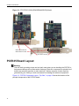
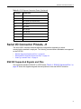
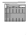
1
PCE335 Hardware
Installation Guide
PCE335
PCI Express® Four-Port
WAN Communications Adapter
Hardware Installation Guide
Performance Technologies
205 Indigo Creek Drive
Rochester, NY 14626
585.256.0200
[email protected]
www.pt.com
© 2008 Performance Technologies, Inc.
All Rights Reserved.
Document Revision History
Part Number
Date
Explanation of Changes
106p0335.10
December 11, 2007
Initial Release
106p0335.11
January 31, 2008
Clarified up-plugging installation of the PCE335.
106p0335.12
May 12, 2008
Clarified introduction to PCE335 Cable Pinouts.
106p0335.13
December 22, 2008
Updated images and text to reflect black jackpost replaced on
PCE335 Front Panel.
Copyright Notice
© Copyright 2008 by Performance Technologies, Inc. All Rights Reserved.
The Performance Technologies logo is a registered trademark of Performance Technologies,
Inc. All other product and brand names may be trademarks or registered trademarks of their
respective owners.
This document is the sole property of Performance Technologies Inc.
Errors and Omissions
Although diligent efforts are made to supply accurate technical information to the user,
occasionally errors and omissions occur in manuals of this type. Refer to the Performance
Technologies, Inc. Web site to obtain manual revisions or current customer information:
http://www.pt.com.
Performance Technologies, Inc., reserves its right to change product specifications without
notice.
Symbol Conventions
The following symbols appear in this document:
Caution:
There is risk of equipment damage. Follow the instructions.
Warning:
Hazardous voltages are present. To reduce the risk of electrical shock and danger to
personal health, follow the instructions.
Caution:
Electronic components on printed circuit boards are extremely sensitive to static electricity.
Ordinary amounts of static electricity generated by your clothing or work environment can
damage the electronic equipment. It is recommended that anti-static ground straps and antistatic mats are used when installing the board in a system to help prevent damage due to
electrostatic discharge.
Additional safety information is available throughout this guide.
2
Contents
Chapter 1: About This Guide
11
Overview . . . . . . . . . . . . . . . . . . . . . . . . . . . . . . . . . . . . . . . . . . . . . . . . . . . . . . . . . . . . . . . . . . 11
Related Documents . . . . . . . . . . . . . . . . . . . . . . . . . . . . . . . . . . . . . . . . . . . . . . . . . . . . . . . . . 12
Customer Support and Services . . . . . . . . . . . . . . . . . . . . . . . . . . . . . . . . . . . . . . . . . . . . . . . . 13
Customer Support Packages . . . . . . . . . . . . . . . . . . . . . . . . . . . . . . . . . . . . . . . . . . . . . . . 13
Other Web Support . . . . . . . . . . . . . . . . . . . . . . . . . . . . . . . . . . . . . . . . . . . . . . . . . . . . . . . 13
Return Merchandise Authorization (RMA) . . . . . . . . . . . . . . . . . . . . . . . . . . . . . . . . . . . . . 13
Product Warranty . . . . . . . . . . . . . . . . . . . . . . . . . . . . . . . . . . . . . . . . . . . . . . . . . . . . . . . . . . . 14
Chapter 2: Introduction
15
Overview . . . . . . . . . . . . . . . . . . . . . . . . . . . . . . . . . . . . . . . . . . . . . . . . . . . . . . . . . . . . . . . . . . 15
Product Summary . . . . . . . . . . . . . . . . . . . . . . . . . . . . . . . . . . . . . . . . . . . . . . . . . . . . . . . . . . . 15
Software . . . . . . . . . . . . . . . . . . . . . . . . . . . . . . . . . . . . . . . . . . . . . . . . . . . . . . . . . . . . . . . 16
PCE335 Configurations and Accessories . . . . . . . . . . . . . . . . . . . . . . . . . . . . . . . . . . . . . . 16
PCE335 Features . . . . . . . . . . . . . . . . . . . . . . . . . . . . . . . . . . . . . . . . . . . . . . . . . . . . . . . . . . . 17
PCE335 Front Panel . . . . . . . . . . . . . . . . . . . . . . . . . . . . . . . . . . . . . . . . . . . . . . . . . . . . . . . . . 17
PCE335 Board Layout . . . . . . . . . . . . . . . . . . . . . . . . . . . . . . . . . . . . . . . . . . . . . . . . . . . . . . . 18
Chapter 3: Installation
21
Overview . . . . . . . . . . . . . . . . . . . . . . . . . . . . . . . . . . . . . . . . . . . . . . . . . . . . . . . . . . . . . . . . . . 21
Unpacking . . . . . . . . . . . . . . . . . . . . . . . . . . . . . . . . . . . . . . . . . . . . . . . . . . . . . . . . . . . . . . . . . 22
3
Contents
Connectivity . . . . . . . . . . . . . . . . . . . . . . . . . . . . . . . . . . . . . . . . . . . . . . . . . . . . . . . . . . . . . . . 22
Installing the PCE335 . . . . . . . . . . . . . . . . . . . . . . . . . . . . . . . . . . . . . . . . . . . . . . . . . . . . . . . . 22
Replacing the I/O Bracket . . . . . . . . . . . . . . . . . . . . . . . . . . . . . . . . . . . . . . . . . . . . . . . . . . 24
Connecting the Cable . . . . . . . . . . . . . . . . . . . . . . . . . . . . . . . . . . . . . . . . . . . . . . . . . . . . . . . . 25
Option Jumper Pack (P4) . . . . . . . . . . . . . . . . . . . . . . . . . . . . . . . . . . . . . . . . . . . . . . . . . . . . . 26
A Note About PCI Express Slots . . . . . . . . . . . . . . . . . . . . . . . . . . . . . . . . . . . . . . . . . . . . . . . . 26
PCIe Slot Details . . . . . . . . . . . . . . . . . . . . . . . . . . . . . . . . . . . . . . . . . . . . . . . . . . . . . . . . . 26
Chapter 4: Development Environment
27
Overview . . . . . . . . . . . . . . . . . . . . . . . . . . . . . . . . . . . . . . . . . . . . . . . . . . . . . . . . . . . . . . . . . . 27
PCE335 Functional Blocks . . . . . . . . . . . . . . . . . . . . . . . . . . . . . . . . . . . . . . . . . . . . . . . . . . . . 28
MPC8270 PowerQUICC II Processor . . . . . . . . . . . . . . . . . . . . . . . . . . . . . . . . . . . . . . . . . . . . 28
Reset Logic . . . . . . . . . . . . . . . . . . . . . . . . . . . . . . . . . . . . . . . . . . . . . . . . . . . . . . . . . . . . . . . . 29
Power-On Reset . . . . . . . . . . . . . . . . . . . . . . . . . . . . . . . . . . . . . . . . . . . . . . . . . . . . . . . . . 29
Hard Reset . . . . . . . . . . . . . . . . . . . . . . . . . . . . . . . . . . . . . . . . . . . . . . . . . . . . . . . . . . . . . 29
Soft Reset . . . . . . . . . . . . . . . . . . . . . . . . . . . . . . . . . . . . . . . . . . . . . . . . . . . . . . . . . . . . . . 30
PCI Express Interface Resets . . . . . . . . . . . . . . . . . . . . . . . . . . . . . . . . . . . . . . . . . . . . . . . 30
Memory Map . . . . . . . . . . . . . . . . . . . . . . . . . . . . . . . . . . . . . . . . . . . . . . . . . . . . . . . . . . . . . . . 31
Communication Processor Interrupt Sources . . . . . . . . . . . . . . . . . . . . . . . . . . . . . . . . . . . . . . 32
JTAG Support . . . . . . . . . . . . . . . . . . . . . . . . . . . . . . . . . . . . . . . . . . . . . . . . . . . . . . . . . . . . . . 33
Processor Support . . . . . . . . . . . . . . . . . . . . . . . . . . . . . . . . . . . . . . . . . . . . . . . . . . . . . . . 33
Logic Port . . . . . . . . . . . . . . . . . . . . . . . . . . . . . . . . . . . . . . . . . . . . . . . . . . . . . . . . . . . . . . 33
SDRAM . . . . . . . . . . . . . . . . . . . . . . . . . . . . . . . . . . . . . . . . . . . . . . . . . . . . . . . . . . . . . . . . . . . 33
PCI Express Interface . . . . . . . . . . . . . . . . . . . . . . . . . . . . . . . . . . . . . . . . . . . . . . . . . . . . . . . . 33
Physical Layer (Layer 1) . . . . . . . . . . . . . . . . . . . . . . . . . . . . . . . . . . . . . . . . . . . . . . . . . . . 34
Data Link Layer (Layer 2) . . . . . . . . . . . . . . . . . . . . . . . . . . . . . . . . . . . . . . . . . . . . . . . . . . 34
Transaction Layer (Layer 3) . . . . . . . . . . . . . . . . . . . . . . . . . . . . . . . . . . . . . . . . . . . . . . . . 34
Forward Mode . . . . . . . . . . . . . . . . . . . . . . . . . . . . . . . . . . . . . . . . . . . . . . . . . . . . . . . . . . . 34
Non-Transparent Mode . . . . . . . . . . . . . . . . . . . . . . . . . . . . . . . . . . . . . . . . . . . . . . . . . . . . 35
PCI Express Interrupts . . . . . . . . . . . . . . . . . . . . . . . . . . . . . . . . . . . . . . . . . . . . . . . . . . . . 35
Flash Memory . . . . . . . . . . . . . . . . . . . . . . . . . . . . . . . . . . . . . . . . . . . . . . . . . . . . . . . . . . . . . . 36
EEPROM Device . . . . . . . . . . . . . . . . . . . . . . . . . . . . . . . . . . . . . . . . . . . . . . . . . . . . . . . . . . . 36
4
Contents
User I/O . . . . . . . . . . . . . . . . . . . . . . . . . . . . . . . . . . . . . . . . . . . . . . . . . . . . . . . . . . . . . . . . . . . 36
Serial I/O Connection . . . . . . . . . . . . . . . . . . . . . . . . . . . . . . . . . . . . . . . . . . . . . . . . . . . . . 36
Console Port . . . . . . . . . . . . . . . . . . . . . . . . . . . . . . . . . . . . . . . . . . . . . . . . . . . . . . . . . . . . 37
Clock Steering . . . . . . . . . . . . . . . . . . . . . . . . . . . . . . . . . . . . . . . . . . . . . . . . . . . . . . . . . . . . . . 37
User-Configurable Switches . . . . . . . . . . . . . . . . . . . . . . . . . . . . . . . . . . . . . . . . . . . . . . . . . . . 37
Option Jumper Pack . . . . . . . . . . . . . . . . . . . . . . . . . . . . . . . . . . . . . . . . . . . . . . . . . . . . . . . . . 38
Optional BDM Port . . . . . . . . . . . . . . . . . . . . . . . . . . . . . . . . . . . . . . . . . . . . . . . . . . . . . . . . . . 38
Chapter 5: Connectors
39
Overview . . . . . . . . . . . . . . . . . . . . . . . . . . . . . . . . . . . . . . . . . . . . . . . . . . . . . . . . . . . . . . . . . . 39
PCI Express Connector Pinout . . . . . . . . . . . . . . . . . . . . . . . . . . . . . . . . . . . . . . . . . . . . . . . . . 40
Serial I/O Connector Pinouts, J1 . . . . . . . . . . . . . . . . . . . . . . . . . . . . . . . . . . . . . . . . . . . . . . . . 41
RS232C Supported Signals and Pins . . . . . . . . . . . . . . . . . . . . . . . . . . . . . . . . . . . . . . . . . 41
RS422/449/530 Supported Signals and Pins . . . . . . . . . . . . . . . . . . . . . . . . . . . . . . . . . . . 44
Cable Type Indicator Pins . . . . . . . . . . . . . . . . . . . . . . . . . . . . . . . . . . . . . . . . . . . . . . . . . . 51
Console Serial Port Pinout, J1 . . . . . . . . . . . . . . . . . . . . . . . . . . . . . . . . . . . . . . . . . . . . . . . . . 51
Logic JTAG Port Pinout, P1 . . . . . . . . . . . . . . . . . . . . . . . . . . . . . . . . . . . . . . . . . . . . . . . . . . . 52
COPS JTAG Pinout, P2 . . . . . . . . . . . . . . . . . . . . . . . . . . . . . . . . . . . . . . . . . . . . . . . . . . . . . . 53
Console Serial Port Pinout, Internal Header, P3 . . . . . . . . . . . . . . . . . . . . . . . . . . . . . . . . . . . . 54
Option Jumper Header, P4 . . . . . . . . . . . . . . . . . . . . . . . . . . . . . . . . . . . . . . . . . . . . . . . . . . . . 54
PCE335 Cable Pinouts . . . . . . . . . . . . . . . . . . . . . . . . . . . . . . . . . . . . . . . . . . . . . . . . . . . . . . . 55
RS232C Cable Pinout . . . . . . . . . . . . . . . . . . . . . . . . . . . . . . . . . . . . . . . . . . . . . . . . . . . . . 55
RS449 Cable Pinout . . . . . . . . . . . . . . . . . . . . . . . . . . . . . . . . . . . . . . . . . . . . . . . . . . . . . . 59
RS530 Cable Pinout . . . . . . . . . . . . . . . . . . . . . . . . . . . . . . . . . . . . . . . . . . . . . . . . . . . . . . 64
Chapter 6: MPC8270 I/O Ports
69
Overview . . . . . . . . . . . . . . . . . . . . . . . . . . . . . . . . . . . . . . . . . . . . . . . . . . . . . . . . . . . . . . . . . . 69
Serial Management Controllers . . . . . . . . . . . . . . . . . . . . . . . . . . . . . . . . . . . . . . . . . . . . . . . . 69
MPC8270 Parallel Port Pin Assignments . . . . . . . . . . . . . . . . . . . . . . . . . . . . . . . . . . . . . . . . . 70
MPC8270 Port A Pin Assignments . . . . . . . . . . . . . . . . . . . . . . . . . . . . . . . . . . . . . . . . . . . 70
MPC8270 Port B Pin Assignments . . . . . . . . . . . . . . . . . . . . . . . . . . . . . . . . . . . . . . . . . . . 72
MPC8270 Port C Pin Assignments . . . . . . . . . . . . . . . . . . . . . . . . . . . . . . . . . . . . . . . . . . . 74
5
Contents
MPC8270 Port D Pin Assignments . . . . . . . . . . . . . . . . . . . . . . . . . . . . . . . . . . . . . . . . . . . 76
Chapter 7: Specifications
79
Overview . . . . . . . . . . . . . . . . . . . . . . . . . . . . . . . . . . . . . . . . . . . . . . . . . . . . . . . . . . . . . . . . . . 79
Environmental Requirements . . . . . . . . . . . . . . . . . . . . . . . . . . . . . . . . . . . . . . . . . . . . . . . . . . 80
Power Requirements . . . . . . . . . . . . . . . . . . . . . . . . . . . . . . . . . . . . . . . . . . . . . . . . . . . . . . . . 80
Mechanical Specifications . . . . . . . . . . . . . . . . . . . . . . . . . . . . . . . . . . . . . . . . . . . . . . . . . . . . . 81
Reliability . . . . . . . . . . . . . . . . . . . . . . . . . . . . . . . . . . . . . . . . . . . . . . . . . . . . . . . . . . . . . . . . . . 81
Chapter 8: Agency Approvals, Safety Information, and Data Sheets
83
Overview . . . . . . . . . . . . . . . . . . . . . . . . . . . . . . . . . . . . . . . . . . . . . . . . . . . . . . . . . . . . . . . . . . 83
Certifications . . . . . . . . . . . . . . . . . . . . . . . . . . . . . . . . . . . . . . . . . . . . . . . . . . . . . . . . . . . . . . . 83
CE Certification . . . . . . . . . . . . . . . . . . . . . . . . . . . . . . . . . . . . . . . . . . . . . . . . . . . . . . . . . . 84
Regulatory Information . . . . . . . . . . . . . . . . . . . . . . . . . . . . . . . . . . . . . . . . . . . . . . . . . . . . . . . 84
FCC (USA) Class A Notice . . . . . . . . . . . . . . . . . . . . . . . . . . . . . . . . . . . . . . . . . . . . . . . . . 84
ICES-003 (Canada) Class A Notice . . . . . . . . . . . . . . . . . . . . . . . . . . . . . . . . . . . . . . . . . . 85
Product Safety Information . . . . . . . . . . . . . . . . . . . . . . . . . . . . . . . . . . . . . . . . . . . . . . . . . . . . 85
Compliance with RoHS and WEEE Directives . . . . . . . . . . . . . . . . . . . . . . . . . . . . . . . . . . . . . 86
Data Sheet Reference . . . . . . . . . . . . . . . . . . . . . . . . . . . . . . . . . . . . . . . . . . . . . . . . . . . . . . . 86
PCI Express Specifications . . . . . . . . . . . . . . . . . . . . . . . . . . . . . . . . . . . . . . . . . . . . . . . . . 86
User Documentation References . . . . . . . . . . . . . . . . . . . . . . . . . . . . . . . . . . . . . . . . . . . . 87
Index
6
89
Ta b l e s
Table 4-1: Reset Priorities . . . . . . . . . . . . . . . . . . . . . . . . . . . . . . . . . . . . . . . . . . . . . . . . . . . . . . . . 29
Table 4-2: MPC8270 Chip-Select Assignments . . . . . . . . . . . . . . . . . . . . . . . . . . . . . . . . . . . . . . . 31
Table 4-3: Communication Processor Interrupt Sources . . . . . . . . . . . . . . . . . . . . . . . . . . . . . . . . . 32
Table 5-1: PCI Express Connector Pinout. . . . . . . . . . . . . . . . . . . . . . . . . . . . . . . . . . . . . . . . . . . . 40
Table 5-2: RS232C Signals and Pins . . . . . . . . . . . . . . . . . . . . . . . . . . . . . . . . . . . . . . . . . . . . . . . 42
Table 5-3: RS422/449/530 Signals and Pins. . . . . . . . . . . . . . . . . . . . . . . . . . . . . . . . . . . . . . . . . . 45
Table 5-4: Cable Type Indicator Pins . . . . . . . . . . . . . . . . . . . . . . . . . . . . . . . . . . . . . . . . . . . . . . . 51
Table 5-5: Console Serial Port Pinout, J1 . . . . . . . . . . . . . . . . . . . . . . . . . . . . . . . . . . . . . . . . . . . . 51
Table 5-6: Logic JTAG Pinout, P1 . . . . . . . . . . . . . . . . . . . . . . . . . . . . . . . . . . . . . . . . . . . . . . . . . . 52
Table 5-7: COPS JTAG Pinouts, P2 . . . . . . . . . . . . . . . . . . . . . . . . . . . . . . . . . . . . . . . . . . . . . . . . 53
Table 5-8: Console Serial Port Pinout, Internal Header, P3 . . . . . . . . . . . . . . . . . . . . . . . . . . . . . . 54
Table 5-9: Jumper Pack Functions and Default Settings, P4 . . . . . . . . . . . . . . . . . . . . . . . . . . . . . 54
Table 5-10: RS232C Connector Pin Assignments. . . . . . . . . . . . . . . . . . . . . . . . . . . . . . . . . . . . . . 55
Table 5-11: RS449 Connector Pin Assignments . . . . . . . . . . . . . . . . . . . . . . . . . . . . . . . . . . . . . . . 59
Table 5-12: RS530 Connector Pin Assignments . . . . . . . . . . . . . . . . . . . . . . . . . . . . . . . . . . . . . . . 64
Table 6-1: MPC8270 Port A Pin Assignments. . . . . . . . . . . . . . . . . . . . . . . . . . . . . . . . . . . . . . . . . 70
Table 6-2: MPC8270 Port B Pin Assignments. . . . . . . . . . . . . . . . . . . . . . . . . . . . . . . . . . . . . . . . . 72
Table 6-3: MPC8270 Port C Pin Assignments. . . . . . . . . . . . . . . . . . . . . . . . . . . . . . . . . . . . . . . . . 74
7
Tables
Table 6-4: MPC8270 Port D Pin Assignments. . . . . . . . . . . . . . . . . . . . . . . . . . . . . . . . . . . . . . . . . 76
Table 7-1: Environmental Requirements . . . . . . . . . . . . . . . . . . . . . . . . . . . . . . . . . . . . . . . . . . . . . 80
Table 7-2: Typical Operating Power Requirements . . . . . . . . . . . . . . . . . . . . . . . . . . . . . . . . . . . . . 80
Table 7-3: Mechanical Design . . . . . . . . . . . . . . . . . . . . . . . . . . . . . . . . . . . . . . . . . . . . . . . . . . . . . 81
Table 7-4: Mean Time Between Failures (MTBF) . . . . . . . . . . . . . . . . . . . . . . . . . . . . . . . . . . . . . . 81
8
Figures
Figure 2-1: PT-PCE335-12204 (RS422/RS449/RS530) Model . . . . . . . . . . . . . . . . . . . . . . . . . . . . 18
Figure 2-2: PCE335 Component Layout - Top Side . . . . . . . . . . . . . . . . . . . . . . . . . . . . . . . . . . . . 19
Figure 3-1: PCE335 Insertion Diagram . . . . . . . . . . . . . . . . . . . . . . . . . . . . . . . . . . . . . . . . . . . . . . 23
Figure 3-2: PCE335 I/O Bracket . . . . . . . . . . . . . . . . . . . . . . . . . . . . . . . . . . . . . . . . . . . . . . . . . . . 24
Figure 3-3: PCE335 Cable Alignment . . . . . . . . . . . . . . . . . . . . . . . . . . . . . . . . . . . . . . . . . . . . . . . 25
Figure 3-4: Types of PCI and PCIe Slots. . . . . . . . . . . . . . . . . . . . . . . . . . . . . . . . . . . . . . . . . . . . . 26
Figure 4-1: PCE335 Functional Block Diagram . . . . . . . . . . . . . . . . . . . . . . . . . . . . . . . . . . . . . . . . 28
Figure 7-1: PCE335 Board Dimensions. . . . . . . . . . . . . . . . . . . . . . . . . . . . . . . . . . . . . . . . . . . . . . 81
9
Figures
10
Chapter
1
About This Guide
Overview
This guide describes the hardware-specific functionality and usage of the Performance
Technologies’ PCE335 PCI Express® Four-Port WAN Communications Adapter. In these
chapters you will find installation and configuration information, plus a functional block
description intended for the application developer of this board. Here is a brief description of
what you will find in this guide:
Chapter 1, “About This Guide”, this chapter, provides links to all chapters and appendices in
this guide, plus related documents, customer support and services, and product warranty
information.
Chapter 2, “Introduction,” on page 15 provides a product summary, an overview of product
features, and the information about component layout of the board and the cover faceplate.
Chapter 3, “Installation,” on page 21 provides information about installing the PCE335, and
replacing the faceplate, as well as information about the PCE335 cables. Additionally, there is a
note about PCI Express slots.
Chapter 4, “Development Environment,” on page 27 provides information about the functional
blocks on the board, the processor, reset logic, memory, interrupt sources, JTAG support, PCI
Express interface, flash memory, user I/O, clock steering, and the user-configurable switches.
Chapter 5, “Connectors,” on page 39 provides information about the pinouts and connectors on
the PCE335, including: PCI Express connector, serial I/O connectors, console serial port
pinouts, logic and COPS JTAG port pinout, the optional jumper header, and the cable pinouts.
Chapter 6, “MPC8270 I/O Ports,” on page 69 provides information about the two generalpurpose serial management controllers and the four general-purpose parallel I/O ports on the
communications processor module.
11
Chapter 1: About This Guide
Chapter 7, “Specifications,” on page 79 provides information about the system requirements for
the PCE335 including the environmental and power requirements, mechanical specifications,
and reliability data.
Chapter 8, “Agency Approvals, Safety Information, and Data Sheets,” on page 83 presents
agency approval and certification information for the PCE335. It also provides a summary of
the safety recommendations throughout this manual, as well as information about the data
sheets, standards, and specifications for the technology designed into PCE335.
An “Index,” on page 89 is also provided.
Related Documents
This product is compatible with the complete suite of Performance Technologies software. The
PCE335 assembly should be used in conjunction with the Performance Technologies software
package that you have chosen, for example:
•
NexusWare® Core
•
NexusWare Wan Protocol
•
HDLC
•
FRAME Relay
•
X.25
•
Radar Receiver
•
TADIL-B
•
Async
See “User Documentation References,” on page 87 for a description of these software
packages. Full documentation to support the additional components that you purchased from
Performance Technologies is available at http://www.pt.com under the product you are
inquiring about.
The following documents may also be useful and are available from the specific vendor’s Web
site:
•
PCI Local Bus Specification, Revision 2.2, 1998. PCI Special Interest Group. http://www.pcisig.com/
specifications/
•
PCI Express Base Specification Revision 1.0. PCI Special Interest Group
•
PCI Express Card Electromechanical Specification Revision 1.0. PCI Special Interest Group
•
Freescale™ MPC603e RISC Microprocessor User’s Manual. http://www.freescale.com/
•
Freescale MPC8280 PowerQUICC™ II Family User’s Manual1
•
Freescale MPC8280 PowerQUICC II Family Reference Manual1
•
Freescale MPC8280 PowerQUICC II Family Hardware Specifications1
•
Freescale MPC8280 PowerQUICC II Family Device Errata1
•
Freescale MPC8280 PowerQUICC II Family Technical Summary1
•
Pericom PI7C9X110 PCI Express-to-PCI Reversible Bridge Data Sheet. http://www.pericom.com/
•
Electronic Industries Alliance (EIA) RS232C, RS422, and RS530 Specifications
1. The PCE335 uses a Freescale MPC8270 PowerQUICC II CPU, which is discussed in the MPC8280 family documentation.
12
Customer Support and Services
Customer Support and Services
Performance Technologies offers a variety of standard and custom support packages to ensure
customers have access to the critical resources that they need to protect and maximize
hardware and software investments throughout the development, integration, and deployment
phases of the product life cycle.
If you encounter difficulty in using this Performance Technologies, Inc. product, you may
contact our support personnel by:
1. EMAIL (Preferred Method) – Email us at the addresses listed below or use our online email support
form. Outline your problem in detail. Please include your return email address and a telephone
number.
2. TELEPHONE – Contact us via telephone at the number listed below, and request Technical Support.
Our offices are open Monday to Friday, 8:00 a.m. to 8:00 p.m. (Eastern Standard Time).
Performance Technologies Support Contact Information
Embedded Systems and Software
(Includes Platforms, Blades, and Servers)
SS7 Systems
(Includes SEGway™)
Email
[email protected]
[email protected]
Phone
+1 (585) 256-0248
(Monday to Friday, 8 a.m. to 8 p.m.
Eastern Standard Time)
+1 (585) 256-0248
(Monday to Friday, 8 a.m. to 8 p.m.
Eastern Standard Time)
If you are located outside North America, we encourage you to contact the local Performance
Technologies’ distributor or agent for support. Many of our distributors or agents maintain
technical support staffs.
Customer Support Packages
Our configurable development and integration support packages help customers maximize
engineering efforts and achieve time-to-market goals. To find out more about our Customer
Support packages, visit http://www.pt.com/page/support/.
Other Web Support
Support for existing products including manuals, release notes, and drivers can be found on
specific product pages at http://www.pt.com. Use the product search to locate the information
you need.
Return Merchandise Authorization (RMA)
To submit a return merchandise authorization (RMA) request, complete the online RMA form
available at http://pt.com/assets/lib/files/rma-request-form.doc and follow the instructions on
the form. You will be notified with an RMA number once your return request is approved.
Shipping information for returning the unit to Performance Technologies will be provided once
the RMA is issued.
13
Chapter 1: About This Guide
Product Warranty
Performance Technologies, Incorporated, warrants that its products sold hereunder will at the
time of shipment be free from defects in material and workmanship and will conform to
Performance Technologies’ applicable specifications or, if appropriate, to Buyer’s specifications
accepted by Performance Technologies in writing. If products sold hereunder are not as
warranted, Performance Technologies shall, at its option, refund the purchase price, repair, or
replace the product provided proof of purchase and written notice of nonconformance are
received by Performance Technologies within 12 months of shipment, or in the case of
software and integrated circuits within ninety (90) days of shipment and provided said
nonconforming products are returned F.O.B. to Performance Technologies’s facility no later
than thirty days after the warranty period expires. Products returned under warranty claims
must be accompanied by an approved Return Material Authorization number issued by
Performance Technologies and a statement of the reason for the return. Please contact
Performance Technologies, or its agent, with the product serial number to obtain an RMA
number. If Performance Technologies determines that the products are not defective, Buyer
shall pay Performance Technologies all costs of handling and transportation. This warranty
shall not apply to any products Performance Technologies determines to have been subject to
testing for other than specified electrical characteristics or to operating and/or environmental
conditions in excess of the maximum values established in applicable specifications, or have
been subject to mishandling, misuse, static discharge, neglect, improper testing, repair,
alteration, parts removal, damage, assembly or processing that alters the physical or electrical
properties. This warranty excludes all cost of shipping, customs clearance and related charges
outside the United States. Products containing batteries are warranted as above excluding
batteries.
THIS WARRANTY IS IN LIEU OF ALL OTHER WARRANTIES WHETHER EXPRESS,
IMPLIED OR STATUTORY INCLUDING IMPLIED WARRANTIES OF MERCHANTABILITY OR
FITNESS. IN NO EVENT SHALL PERFORMANCE TECHNOLOGIES BE LIABLE FOR ANY
INCIDENTAL OR CONSEQUENTIAL DAMAGES DUE TO BREACH OF THIS WARRANTY
OR ANY OTHER OBLIGATION UNDER THIS ORDER OR CONTRACT.
14
Chapter
2
Introduction
Overview
The PCE335 Multi-Purpose Intelligent WAN Communications Adapter is a four-channel serial
communications adapter for Peripheral Component Interconnect (PCI) Express-based
systems. This product provides four high-speed serial channel interfaces for high performance
synchronous communications on a PCI Express host system.
Topics covered in this chapter include:
•
“Product Summary,” on page 15
•
“PCE335 Features,” on page 17
•
“PCE335 Front Panel,” on page 17
•
“PCE335 Board Layout,” on page 18
Product Summary
The PCE335 provides four serial channel interfaces for high performance synchronous
communications on a PCI Express host system. The architecture capitalizes on the intelligence
of the Freescale MPC8270 Quad Integrated Communications Controller (PowerQUICC II) and
a Pericom PI7C9X110 PCI Express to PCI interface. Code storage and data buffering are
provided by a 128MB SDRAM array, which is available to both the PowerQUICC II and the
PI7C9X110. Additional code space is available onboard in the form of a 32MB application flash
device.
15
Chapter 2: Introduction
Serial line electrical interfacing is available onboard providing voltage level adaptation to a
recommended standard, such as RS232C or RS422 (RS449 or RS530 cabling). The serial line
interface connection on the PCE335 uses a dual VHDCI 136 pin receptacle containing the
signals for all four ports. To provide an industry standard connection for each port, hydra
adapter cables are offered. Adapter cable wiring details for each style cable are also provided.
See “PCE335 Cable Pinouts,” on page 55. The PCE335 supports an optional crystal oscillator
to provide custom synchronous clock speeds. A single green LED is provided as a softwarecontrolled indicator.
Software
The PCE335 integrates the NexusWare WAN communications software suite, which provides
complete WAN connectivity solutions for Radar Receiver/SBSI, Frame Relay, HDLC/LAPD,
and X.25 protocols. The NexusWare Core Linux-based development environment is also
supported. Operating system support includes Solaris™, Windows®, and Linux®. For more
information, visit http://www.pt.com and view our software.
PCE335 Configurations and Accessories
There are currently two models of the PCE335 board:
•
Model PT-PCE335-12180 (PCI Express Four Port RS232C)
•
Model PT-PCE335-12204 (PCI Express Four Port RS422/RS449/RS530)
Note: The instructions and information provided in this manual apply to both models. When
values and options differ for each model, they are noted.
Figure 2-1, “PT-PCE335-12204 (RS422/RS449/RS530) Model,” on page 18 displays a
photograph of the PT-PCE335-12204 (RS422/RS449/RS530) model showing both the
standard height I/O bracket (front panel) on the right and the low profile I/O bracket (front panel)
on the left. Note the black jackpost on the front panel; see “Connecting the Cable,” on page 25
for more information about the jackposts. See “Installing the PCE335,” on page 22 for more
information about installation.
Cable Options
Optional hydra cables allow the choice of RS232C, RS449, EIA530, or V.35 connections
depending on the model of PCE335. The following four-position 6ft hydra cables, which must
be ordered separately, are available for use with the PCE335:
•
PT-ACC335-12233: Cable with Console, RS232C (male DB-25 connector)
•
PT-ACC335-12234: Cable without Console, RS232C (male DB-25 connector)
•
PT-ACC335-12203: Cable with Console, RS449 (male DB-37 connector)
•
PT-ACC335-12205: Cable without Console, RS449 (male DB-37 connector)
•
PT-ACC335-12256: Cable with Console, EIA530 (male DB-25 connector)
•
PT-ACC335-12257: Cable without Console, EIA530 (male DB-25 connector)
•
PT-ACC335-12290: Cable with Console, V.35 (male M34 connector)
•
PT-ACC335-12291: Cable without Console, V.35 (male M34 connector)
The PCE335 ships with the appropriate hydra cable for the model ordered. See “PCE335
Cable Pinouts,” on page 55 for information about the cable pinouts.
16
PCE335 Features
PCE335 Features
The PCE335 contains the following hardware and software features:
•
Four high-speed channels capable of sustaining 2Mbps bi-directional per port
•
Simultaneously sustained 8Mbps maximum line speed
•
Freescale MPC8270 PowerQUICC II processor (266MHz)
•
128MB dedicated processor SDRAM memory
•
32MB of on-board flash storage
•
Physical Interface: RS422 or RS232C User Console, PCI Express x1 Lane
•
NexusWare Core Linux-based development environment and operating system
•
Integrated NexusWare WAN communications software including Radar Receiver/SBSI, HDLC,
Frame-Relay, LAPD, and X.25 protocols
•
Operating system support includes Solaris, Windows, and Linux
•
Configurable with either standard height (full height) or low profile (half height) front panel
PCE335 Front Panel
The PCE335 can be configured with either a standard height (full height) front panel or a low
profile (half height) front panel with openings for the serial port connector. See Figure 2-1, “PTPCE335-12204 (RS422/RS449/RS530) Model,” on page 18.
Note: All models of the PCE335 are shipped with the standard height (full height) I/O bracket
(front panel). A low profile (half height) I/O bracket (front panel) is also shipped with every
board. See the instructions in the section “Replacing the I/O Bracket,” on page 24 if you need to
use the low-profile front panel.
17
Chapter 2: Introduction
Figure 2-1: PT-PCE335-12204 (RS422/RS449/RS530) Model
Black Jackpost mates with
Black Jackscrew on Cable
Dual VHDCI Connectors
PCE335 Board Layout
Warning:
Use anti-static grounding straps and anti-static mats when you are handling the PCE335 to
help prevent damage due to electrostatic discharge. Electronic components on printed circuit
boards are extremely sensitive to static electricity. Ordinary amounts of static electricity
generated by your clothing or work environment can damage the electronic equipment.
Figure 2-2, “PCE335 Component Layout - Top Side,” on page 19 shows the location of the
principal components of the PCE335 board.
18
PCE335 Board Layout
Figure 2-2: PCE335 Component Layout - Top Side
19
Chapter 2: Introduction
20
Chapter
3
Installation
Overview
This chapter provides information about installing the PCE335 in a PCIe slot on a computer
chassis. You will also find information about replacing the front panel and connecting the cable
to the PCE335 after installation.
Topics covered in this chapter include:
•
“Unpacking,” on page 22
•
“Connectivity,” on page 22
•
“Installing the PCE335,” on page 22
•
“Connecting the Cable,” on page 25
•
“Option Jumper Pack (P4),” on page 26
•
“A Note About PCI Express Slots,” on page 26
21
Chapter 3: Installation
Unpacking
Before unpacking the module, visually inspect the packing container for any damage that might
have occurred during shipment from the factory. If the container appears damaged,
immediately contact the company responsible for the shipping and report the damage before
opening and unpacking the container. It is recommended that you also notify Performance
Technologies (see “Customer Support and Services,” on page 13 for assistance information).
Before you connect your system and install the software, verify using the packing slip that you
received all the components. If you are missing any of the components shown on the packing
slip, contact your Performance Technologies Sales Representative immediately.
Caution:
The module is packed in an antistatic bag to protect it during shipment. Keep the module in
its protective antistatic bag until you are ready to install it in the carrier platform. To prevent
damage to the module due to electrostatic discharge, wear a grounding strap and handle the
module only by its edges. To reduce the risk of damage to the PCE335, the module must be
protected from electrostatic discharge and physical shock. Never remove any of the
socketed parts except in a static-free environment. Use the anti-static bag shipped with the
product to handle the module.
Caution:
Do not touch its components or any metal parts other than the front panel. Avoid touching
areas of integrated circuitry. Static discharge can damage these circuits.
Connectivity
The PCE335 provides a dual VHDCI connector for interfacing with application-specific devices.
See Chapter 5, “Connectors,” on page 39 for complete connector descriptions and pinouts.
Installing the PCE335
The PCE335 is shipped with a standard-height (full height) I/O bracket installed. If you need to
install a low-profile I/O bracket, see “Replacing the I/O Bracket,” on page 24.
See “Connecting the Cable,” on page 25 for information about connecting the cable to the
PCE335.
Warning:
Make sure that the computer is turned off and the power cord is detached from the host
chassis prior to installing the PCE335 board. Attempting to install the PCE335 in a computer
chassis that has the power still active could result in electrical shock causing serious injury
or death.
22
Installing the PCE335
Warning:
Use anti-static grounding straps and anti-static mats when you are handling the PCE335 to
help prevent damage due to electrostatic discharge. Electronic components on printed circuit
boards are extremely sensitive to static electricity. Ordinary amounts of static electricity
generated by your clothing or work environment can damage the electronic equipment.
Use these steps to install the PCE335 in a computer chassis:
1. Turn off the power for the computer on which you are installing the PCE335.
2. Remove the rear cover or side panel that allows access to the inside of the computer by removing the
retaining screws or other cover lock down devices.
3. Locate an empty PCIe slot and remove the corresponding slot cover plate from the outside of the PC
chassis. Note that the PCE335 is capable of up-plugging. See “A Note About PCI Express Slots,” on
page 26 for information about PCIe slots and up-plugging.
4. Line up the PCE335 board with the PCIe slot and press the PCE335 into the slot with the cover plate
end of the board over the edge of the main board. Use caution when pressing so you do not snap the
board (see Figure 3-1, “PCE335 Insertion Diagram,” below).
5. Use the retaining screw that was with the cover plate and screw the board cover plate to the chassis.
This step secures the board to the chassis and prevents the board from moving.
6. You can now apply power to the computer.
7. The PCE335 is now ready for application development.
Figure 3-1: PCE335 Insertion Diagram
PCE335
Computer
Chassis
Edge
Connector
Card
Connector
23
Chapter 3: Installation
Replacing the I/O Bracket
Use these steps to replace the standard height I/O bracket with the low profile I/O bracket:
1. Remove and retain the printed circuit board mounting screws, located on the top side of the board.
See Figure 3-2, “PCE335 I/O Bracket,” below.
2. Remove and retain the VHDCI I/O jackposts, located on the front of the I/O bracket. Take note of the
position of the black jackpost at the top right. See Figure 3-2, “PCE335 I/O Bracket,” below.
3. Slip the standard height I/O bracket off the VHDCI I/O connector, noting the bracket’s orientation.
4. Position the low profile I/O bracket over the VHDCI I/O connector in an orientation similar to the
standard height I/O bracket.
5. Use the printed circuit board mounting screws to screw the low profile I/O bracket to the board, on the
top side of the board.
6. Use the VHDCI I/O jackposts to screw the low profile I/O bracket to the VHDCI I/O connector. Return
the black jackpost to the top right position as shown in Figure 3-2, “PCE335 I/O Bracket,” below.
7. Continue with the procedures described above to “Installing the PCE335,” on page 22.
Figure 3-2: PCE335 I/O Bracket
Printed Circuit Board
Mounting Screws
VHDCI I/O Jackposts
(Note black jackpost
at top right.)
24
Connecting the Cable
Connecting the Cable
This section contains cabling information for the PCE335 board.
See “PCE335 Configurations and Accessories,” on page 16 for a list of the cables available for
use with the PCE335. The PCE335 ships with the appropriate four-port hydra cable you have
ordered. See “PCE335 Cable Pinouts,” on page 55 for information about the various cable
pinouts.
Caution:
Before connecting the cable, make sure the retaining screws on the board are tight and the
board is securely seated.
To connect the cable to the PCE335:
1. After installing the PCE335 in the host chassis, align the black jackscrew on the cable with the black
jackpost on the front panel of the board (see Figure 3-3, “PCE335 Cable Alignment,” below).
2. Insert the cable into the dual VHDCI connector.
3. Fasten the four jackscrews to secure the cable.
Figure 3-3: PCE335 Cable Alignment
PCE335
Black Jackpost
Black Jackscrew
Cable Head
Align the black jackscrew on the cable head
with the black jackpost on the front panel
of the module.
25
Chapter 3: Installation
Option Jumper Pack (P4)
A jumper pack at position P4 allows you to configure several board functions.
•
See Figure 2-2, “PCE335 Component Layout - Top Side,” on page 19 to see the location of this
jumper pack.
•
See Table 5-9, “Jumper Pack Functions and Default Settings, P4,” on page 54 for a list of the
jumpers, their default factory settings, and their functions.
A Note About PCI Express Slots
The PCI Express vertical card-edge connectors are specified for Link widths of x1, x4, x8 and
x16. These are not compatible with prior PCI interface standards such as PCI and PCI-X.
Figure 3-4, “Types of PCI and PCIe Slots,” provides examples of the different types of PCI and
PCI Express slots. The PCE335 edge connector utilizes an X1 lane interface. This is capable of
up-plugging; that is, it may be inserted into an X2, X4, X8 or X16 slot. Installation is not
restricted to an X1 slot. Further details are provided in “PCI Express Connections,” on page 34.
Figure 3-4: Types of PCI and PCIe Slots
PCIe Slot Details
PCIe is a high-speed bidirectional peripheral interconnect that includes both a protocol and a
layered architecture that has higher data transfer rates than the original PCI bus. PCIe carries
data in packets along two pairs of point-to-point data lanes, compared to the single parallel data
bus of traditional PCI that routes data at a set rate. Bit rates for PCIe reach 1.25 Gbps per lane
direction, which equates to data transfer rates of approximately 400MBps per lane.
The PCIe bus replaced the standard PCI bus when computer processor speeds started to
exceed the capabilities of the PCI architecture. The PCI is a shared parallel bus architecture,
the PCIe is a high speed serial switched architecture.
26
Chapter
4
Development Environment
Overview
This chapter provides information about the board’s functional blocks, power considerations,
the processor, reset logic, interrupt sources, JTAG support, PCI Express interface, SDRAM,
board memory, flash memory, and other features.
Note: The information contained in this chapter should be used in conjunction with the
software you purchased from Performance Technologies.
Topics covered in this chapter include:
•
“PCE335 Functional Blocks,” on page 28
•
“MPC8270 PowerQUICC II Processor,” on page 28
•
“Reset Logic,” on page 29
•
“Memory Map,” on page 31
•
“Communication Processor Interrupt Sources,” on page 32
•
“JTAG Support,” on page 33
•
“SDRAM,” on page 33
•
“PCI Express Interface,” on page 33
•
“Flash Memory,” on page 36
•
“EEPROM Device,” on page 36
•
“User I/O,” on page 36
•
“Clock Steering,” on page 37
•
“User-Configurable Switches,” on page 37
•
“Option Jumper Pack,” on page 38
•
“Optional BDM Port,” on page 38
27
Chapter 4: Development Environment
PCE335 Functional Blocks
The block diagram in Figure 4-1, “PCE335 Functional Block Diagram,” illustrates the major
components of the board design. The following topics provide overviews of the functional
blocks.
Figure 4-1: PCE335 Functional Block Diagram
Dual
VHDCI
I/O
Connector
(J1)
Clock
Steering
Logic
GeneralPurpose
Switches
(SW1)
Interrupt
Sources
Optional
BDM
Connector
Freescale
MPC8270
PowerQUICC II
Communications
Processor
Module
EEPROM
Non-Volatile
Storage
Console
Serial Port
Header (P3)
Logic
JTAG
Port (P1)
COPS
JTAG
Port (P2)
Power-On
Reset and
Control Logic
Memory
Controller
Option
Jumper
Pack (P4)
Boot and
Application
Flash
PCI Express
Interface
Board-Mounted
SDRAM Array
128MB
PCI Express Bus
MPC8270 PowerQUICC II Processor
The CPU that is used on the PCE335 is a Freescale MPC8270 PowerQUICC II. The MPC8270
is the primary controller on the PCE335. It supplies the PowerPC CPU core, the
Communications Processor Module (CPM), and the 60X bus processor bus controller. It has
direct connections to, and is the controller for the Synchronous DRAM (SDRAM), and the PCI
side of the PI7C9X110 PCI Express Interface Controller. It controls all of the on-board
resources via a buffered data and address bus and a set of local control registers.
For more information on the chip, consult the Freescale, Inc. Web site:
http://www.freescale.com/.
Note: See the list of documents for the Freescale MPC8280 PowerQUICC II Family in
“Related Documents,” on page 12.
28
Reset Logic
Reset Logic
The reset logic for the PCE335 has many components, including major resets caused by the
external PCI Express bus. The resets are described in the following sections:
•
Power-On Reset
•
Hard Reset
•
Soft Reset
•
PCI Express Interface Resets
Table 4-1, “Reset Priorities,” describes the priorities for the on-board resets.
Table 4-1: Reset Priorities
Reset Source
Activated Signal
PORESET
HRESET
SRESET
Local Logic
PORESET
—
X
X
X
HRESET
—
—
X
X
SRESET
—
—
—
X
PCIEXPRST
X
X
X
X
LOCAL PCI RST
—
X
X
X
BREAK Detect
—
X
X
X
Power-On Reset
An on-board reset controller initiates the power-on reset sequence for the board. The device
provides a 20ms reset pulse after the 3.3V power settles to an “intolerance” condition. It will
also activate if there is a brownout condition. The power-on reset signal resets internal logic
and the board peripheral devices.
The power-on reset signal is also issued in response to a PCI Express reset (PCE_PERST#).
Hard Reset
The hard reset signal, PQ_HRESET#, is generated by the PowerQUICC II communications
microprocessor or the on-board control logic. The MPC8270 generates PQ_HRESET# in
response to a power-on reset, a software watchdog reset (if enabled), a bus monitor reset (if
enabled), or a checkstop reset (if enabled). The effect of hard reset on the processor is different
than power-on reset and is outlined in the MPC8270 PowerQUICC II Family User’s Manual in
the Reset chapter, from http://www.freescale.com/.
The on-board control logic generates PQ_HRESET# in response to a System board reset from
the local PCI reset issued by the PI7C9X110 PCI Express Interface. This happens only if the
host system is not generating a PCI Express reset at the same time. The on-board control logic
also asserts PQ_HRESET# in response to the reception of an RS232C BREAK signal on the
console port. This happens if the Break Detect Enable jumper is residing in positions P4-7 to
P4-8. When the PQ_HRESET# signal is asserted because of an RS232C break, it will remain
asserted until the break signal is removed.
29
Chapter 4: Development Environment
Soft Reset
The MPC8270 asserts this signal in response to any power-on reset or hard-reset condition.
The effect of soft reset on the processor is different than power-on reset or hard reset and is
outlined in the MPC8270 PowerQUICC II Family User’s Manual in the Reset chapter, http://
www.freescale.com/.
PCI Express Interface Resets
The PI7C9X110 interface has more than one reset condition. They are described in the
following sections:
•
Primary PCI Express Reset
•
PCI Express Reset Commands
Primary PCI Express Reset
The PI7C9X110 receives primary resets from the PCI Express Root Complex on the PCI
Express bus via the PCE_PERST# signal. It resets all of the PI7C9X110’s internal logic as well
as initializing the rest of the PCE335’s logic to the power-on reset condition. Refer to the
Pericom PI7C9X110 PCI Express-to-PCI Reversible Bridge Data Sheet, from http://
www.pericom.com/ for a complete description of this reset.
The MPC8270 PORESET# signal is held true as long as the PCI Express Reset is held true.
PCI Express Reset Commands
There are two further reset levels that the PI7C9X110 supports in the PCE335 configuration
(forward nontransparent): Hot Reset and Secondary Bus Reset.
Hot Reset
Hot Reset, Level-1 is received by the PI7C9X110 in the form of a PCI Express in-band
message. It causes the reset of internal registers and state machines, but does not cause the
reset of sticky bits in the internal registers. It also propagates across the bridge, is output on the
local PCI reset signal and causes a hard reset to the MPC8270. Refer to the Pericom
PI7C9X110 PCI Express-to-PCI Reversible Bridge Data Sheet, from http://www.pericom.com/
for a complete description of this reset.
Secondary Bus Reset
The Secondary Bus Reset is invoked by having the internal Bridge Control and Status register
(PI7C9X110 configuration internal memory offset 078h) bit 3 set (Secondary Interface Reset
Bit) by software. This reset takes the bridge state machines to a known state but does not reset
internal registers. This reset also causes the propagation of the Local PCI reset signal as
PERI_PCIRST# and causes a hard reset to the MPC8270. Refer to the Pericom PI7C9X110
PCI Express-to-PCI Reversible Bridge Data Sheet, from http://www.pericom.com/ for a
complete description of this reset. The PCI bus reset condition is sustained until the bit in the
control register is reset. This method is the preferred one to cause a “Software Reset” of the
PCE335.
30
Memory Map
Memory Map
The memory map is defined by the PCE335 address decode scheme. There are different levels
of address decode built into the PCE335. The first level and primary decode is done by the
MPC8270’s System Interface Unit (SIU). One of the SIU’s subsections is the memory
controller. The memory controller is responsible for controlling a maximum of twelve memory
banks shared by a high-performance SDRAM machine, a general-purpose chip-select machine
(GPCM), and three user-programmable machines (UPMs). It supports a glueless interface to
synchronous DRAM (SDRAM), EPROM, flash EPROM, burstable RAM, regular DRAM
devices, extended data output DRAM devices, and other peripherals. This flexible memory
controller allows the implementation of memory systems with very specific timing requirements.
•
The SDRAM machine provides an interface to synchronous DRAMs, using SDRAM pipelining, bank
interleaving, and back-to-back page mode to achieve the highest performance.
•
The GPCM provides interfacing for simpler, lower-performance memory resources and memorymapped devices. The GPCM has inherently lower performance because it does not support bursting.
For this reason, GPCM-controlled banks are used primarily for boot loading and access to lowperformance memory-mapped peripherals.
•
The UPM supports address multiplexing of the external bus, refresh timers, and generation of
programmable control signals for row address and column address strobes to allow for a glueless
interface to DRAMs, burstable SRAMs, and almost any other kind of peripheral. The refresh timers
allow refresh cycles to be initiated. The UPM can be used to generate different timing patterns for the
control signals that govern a memory device. These patterns define how the external control signals
behave during a read, write, burst-read, or burst- write access request. Refresh timers are also
available to periodically generate user-defined refresh cycles.
The primary control of the devices served by the memory controller machines is through the
MPC8270’s external chip-select lines. The specific memory controller setups are defined for
each type of device in the section of the specification that describes the device. Table 4-2,
“MPC8270 Chip-Select Assignments,” represents the primary address decode of the External
chip-select lines.
Table 4-2: MPC8270 Chip-Select Assignments
Chip-Select Line
Controlled Device
Address Range
CS0
Flash Boot PROM
FFF0_0000 to FFF7_FFFF h
CS1
SDRAM
0000_0000 to 07FF_FFFF h
CS2
Not Used
CS3
Not Used
1000_0000 to 10FF_FFFF h
CS4
PAL General Purpose Registers
2000_0000 to 2000_00ff h
CS5
Not Used
CS6
Not Used
CS7
Not Used
CS8
Not Used
CS9
Not Used
31
Chapter 4: Development Environment
Table 4-2: MPC8270 Chip-Select Assignments (Continued)
Chip-Select Line
Controlled Device
CS11
Not Used
None
PI7C9X110 mapped space
Address Range
Operating System Controlled (Part II)
Communication Processor Interrupt Sources
Several multifunction pins are used to supply the communications processor with the direct
connect interrupts from the various board peripherals. The !IRQ0 to !IRQ7 lines are used along
with some of the port C interrupt capable pins. The interrupt sources, for the most part, have
multiple interrupt conditions. For complete information about interrupt causes, refer to the
individual component subsections or the component’s user manual. Table 4-3, “Communication
Processor Interrupt Sources,” shows the connections from the peripheral devices to the
communications processor.
Table 4-3: Communication Processor Interrupt Sources
32
IRQ Level
Controlled Device
IRQ0
NMI Interrupt
IRQ1
Not Used
IRQ2
Not Used
IRQ3
Not Used
IRQ4
Not Used (Was PI7C9X110 general interrupt for INTA inbound interrupts to the MPC8270.)
IRQ5
Not Used
IRQ6
Not Used
IRQ7
Not Used
PC0
WAKE4 - On the RS232C board this bit indicates that there is a valid electrical signal at port 4, on
DCD or TXCI. It does not indicate a mark or space. This is typically used to indicate that a cable is
plugged in and the transmitting element is active.
PC1
WAKE3 - On the RS232C board this bit indicates that there is a valid electrical signal at port 3, on
DCD or TXCI. It does not indicate a mark or space. This is typically used to indicate that a cable is
plugged in and the transmitting element is active.
PC2
WAKE2 - On the RS232C board this bit indicates that there is a valid electrical signal at port 2, on
DCD or TXCI. It does not indicate a mark or space. This is typically used to indicate that a cable is
plugged in and the transmitting element is active.
PC3
WAKE1 - On the RS232C board this bit indicates that there is a valid electrical signal at port 1, on
DCD or TXCI. It does not indicate a mark or space. This is typically used to indicate that a cable is
plugged in and the transmitting element is active.
JTAG Support
JTAG Support
The PCE335 provides the following JTAG testing support.
Processor Support
The JTAG testing port on the communications processor supports the EST Common On-chip
Processor (COP) debugger on the P2 connector. This connector supports the extended 16-pin
COP debugger signaling, but the basic 10-pin signaling devices can be used with an
interposing adapter. See Table 5-7, “COPS JTAG Pinouts, P2,” on page 53 for more
information about the COPs JTAG pinouts.
Logic Port
This JTAG port is used to program the on-board PLD initially through the PLD’s JTAG port on
the P1 connector. When the JTAG_EN# signal on P1 is pulled low, the remaining JTAG items
on the board are introduced to the chain and allow a JTAG test routine to be run on the
assembly. See Table 5-6, “Logic JTAG Pinout, P1,” on page 52 for more information about the
logic JTAG pinouts.
SDRAM
The Synchronous Dynamic Random Access Memory (SDRAM) memory bank is comprised of
individual chips mounted on the component and circuit sides of the base board. The SDRAM
architecture provides the ability to:
•
Synchronously burst data at a high data rate with automatic column address generation
•
Interleave between internal banks in order to hide PRECHARGE time
•
Randomly change column addresses on each clock cycle during a burst access
The total SDRAM memory is 128MB. This SDRAM memory is arranged in four parallel bytes to
give the data bus a 64-bit total width. The integral SDRAM controller takes care of all low level
SDRAM operations including row and column multiplexing, precharge times, and refresh.
PCI Express Interface
The PCE335 uses a PCI-to-PCI Express Bridge (PI7C9X110) to connect the PCE335’s
communications processor to the Host PCI Express root complex. The PI7C9X110 is compliant
with the following specifications:
•
PCI Express Base Specification, Revision 1.0a
•
PCI Express Card Electromechanical Specification, Revision 1.0a
•
PCI Local Bus Specification, Revision 3.0
•
PCI Express to PCI/PCI-X Bridge Specification, Revision 1.0
The PCE335 application is a forward, non-transparent bridging implementation relative to the
PCI Express root complex. In this forward mode, the PI7C9X110 has an x1 PCI Express
upstream port and a 32-bit PCI/PCI-X downstream port running at 66MHz.
33
Chapter 4: Development Environment
PCI Express Connections
The PI7C9X110’s PCI Express connection to the root complex is made via the card edge
fingers, per the PCI Express Card Electromechanical Specification, Revision 1.0a. The
PCE335 utilizes an x1 lane configuration. RX,TX RXCLK, and PERST# are the supported PCI
Express signals. The PRESENT1# and PRESENT2# signals are connected together on the
board for system presence detection. The PCI Express JTAG signals are not used but TDI is
connected to TDO to allow the JTAG data stream to pass through. Primary board power is
drawn through the connector as well. See Table 5-1, “PCI Express Connector Pinout,” on page
40 for the Express Connector pinout.
Local PCI Connections
The local 32 bit PCI bus is connected between the PI7C9X110’s PCI port and the PCI port on
the MPC8270 only. The MPC8270 is the monarch of the bus. It can configure the PI7C9X110’s
PCI port using AD21 as the IDSEL configuration address bit. The PCI bus arbitrator is the
PI7C9X110’s internal arbitrator. It services the MPC8270 on its REQ0#,GNT0# lines.
Physical Layer (Layer 1)
Layer 1, the Physical Layer (PHY) defines the electrical characteristics of PCI Express. This
layer is the basic transmission unit, which consists of two pairs of wires, called a “lane”. Each
pair allows for unidirectional data transmission 1.25 Gbps, so the two pairs combined provide
2.5 Gbps full-duplex communication, without the risk of transmission collision.
Data Link Layer (Layer 2)
Layer 2, the Data Link Layer (DLL) defines the data control for PCI Express. This data link layer
provides link management and data integrity, including error detection and correction. The layer
calculates and appends a Cyclic Redundancy Check (CRC) and a sequence number to the
information sent from the data packet. The CRC verifies that data has been transmitted
correctly from link to link. The sequence number allows proper ordering of the data packets.
Transaction Layer (Layer 3)
Layer 3, the Transaction Layer (TL) connects the lower protocols to the upper layers. This
Transaction Layer appears to the upper layers of the PCI.
The Transaction Layer packetizes and then pre-appends a header to the payload data. This
layer also includes the read and write commands and prior sideband signals (for example,
interrupts and power management requests).
To achieve code compatibility with PCI, PCI Express does not modify the transaction layer.
Forward Mode
In Forward Mode, the configuration cycles originate from the PCI Express link through the
bridge chip and then to the PCI Bus segment.
34
PCI Express Interface
Non-Transparent Mode
The bridge translates all accesses to and from the Root Complex into local 32-bit PCI
accesses. These accesses are passed to a non-transparent PCI-PCI bridge before they are
presented to the MPC8270 on-board CPU. The non-transparent bridge allows the board
assembly to hide the fact that there is a private PCI bus behind the bridge. The non-transparent
mode also allows the PCE335 to identify itself to the ROOT complex with a PTI Device and
Vendor ID. This configuration allows the operating system to recognize the board and load the
correct system drivers.
In Nontransparent Mode, the bridge isolates processor domains on each side by providing a
Type 0 Configuration Header to each CPU on either side of the bridge. Data is transferred
between the domains through the bridge using address translation. This transfer can occur in
either the upstream or downstream direction.
As a nontransparent bridge, configuration accesses occur on both the PCI bus and the PCI
Express port. There are two “hosts” in this configuration and each can access or send data to
devices on both sides of the bridge. Each host has its own memory map for the devices to
which it has access.
PCI Express Interrupts
The PI7C9X110 PCI Express to PCI bridge chip can support both INT-x emulation of the legacy
INT-x wires or the Message Signaled Interrupt (MSI) mode of interrupt passing on either side of
the bridge. The PCE335 is designed to support both modes of operation. The selection of the
mode of operation will be up to the Root Complex software driver and is dependent on the
hardware and software capabilities of the particular system in which the PCE335 is installed.
The bridge chip also imposes a limitation on modes by only allowing the same type of operation
on either side (PCI or PCI Express) of itself, once one particular mode is chosen. This forces a
change on how the interrupts are handled in the hardware and software so that a consistent
interrupt method is used in either mode. The operating features are outlined in the following
sections.
Outbound Interrupts
The method for creating an outbound interrupt is the same whether INT-x or MSI is chosen as
the operating mode. The outbound interrupt is generated by the MPC8270 by using
PI7C9X110’s Primary IRQ register set to send an interrupt message to the host. Access to the
registers is by the local PCI bus.
After writing the Primary IRQ, depending on the method chosen by the Root Complex OS and
device driver, the PI7C9X110 will generate either a legacy INT-x serial message to the host or
an MSI message to the host. The interrupt message is mapped to the PCE335’s Root Complex
OS interrupt handler and the appropriate action can then be taken by the interrupt handler. The
PI7C9X110 Primary IRQ register set is used to signal a particular interrupt event and the
PI7C9X110 scratchpad registers can be used for argument and message passing.
35
Chapter 4: Development Environment
Inbound Interrupts
Inbound Interrupt will be routed through the PI7C9X110 directly to the MPC8270's PCI Doorbell
register. The board resident code will open up the appropriate PCI windows and expose the
PCI doorbell for use with the PTI drivers.
Flash Memory
The Flash Erasable Programmable Read Only Memory (EPROM) is used to store boot and
application code for the MPC8270. The EPROM is permanently mounted to the PCE335 PCB.
The flash is a non-volatile memory that has the following general characteristics:
•
For access purposes, the device has 256 blocks of byte wide data storage. The storage blocks have
128K bytes of storage each.
•
Selecting, writing and erasing the blocks is done by using a Common Flash Interface (CFI) and a
Scaleable Command Set (SCS).
The PCE335 has a write-protect feature that does not allow the write signal to activate unless
the flash_wp bit is set in the general purpose registers. After a reset, writing to the flash is
disabled, by default.
EEPROM Device
A small EEPROM device is connected to port A on the MPC8270, which can be used to store
non-volatile information for the operating system or the application code. Reading and writing
this device is currently under direct control of the operating system.
User I/O
The user I/O on the PCE335 consists of the serial I/O connector and a console port. Each is
described below.
Serial I/O Connection
The serial I/O connection for the PCE335 is made through a dual VHDCI connector with 136
pins. See Figure 2-2, “PCE335 Component Layout - Top Side,” on page 19 to see the location
of this connector. See Table 5-5, “Console Serial Port Pinout, J1,” on page 51 for the console
serial port pinout on this connector. Each port is configured to be a Data Terminal Equipment
(DTE) connection and supports the following signals:
RS232C Build
36
•
EIA RS232C single ended input connections conforming to the V.28 electrical characteristics for
RXD, TXCI, RXC, DCD, DSR, CTS with built-in 5K pulldowns
•
Tri-State capable single ended output connections conforming to the V.28 electrical characteristics for
TXD, DTR, RTS, TXC
•
Signal ground
Clock Steering
RS422 Build
•
Supports an RS422 electrical connection for RS449 and RS530 physical connections, through the
use of a hydra breakout cable. See “Connecting the Cable,” on page 25 for information about the
PCE335 cables
•
Differential input connections conforming to the V.11 electrical standards for RXD, TXCI, RXC, DCD,
DSR, and CTS. Each input is terminated with 100 Ohms differentially and a high impedance pullup
and pulldown to ensure idle port condition if no external cable is present
•
Tri-state capable differential output connections conforming to the V.11 electrical standards for TXD,
DTR, RTS, and TXC
•
Supports baud rates up to 2Mbits/sec per port
•
Signal ground
Console Port
The console port can be used through NexusWare to configure and control the board-level
application software. It is implemented as a three-pin right-angle header mounted towards the
upper card edge. There is also nine-pin D-sub female connector on special debug I/O cables
that can be ordered as a development tool. The port is an asynchronous RS232C serial I/O
port that supports the following signals:
•
EIA RS232C single ended input connection conforming to the V.28 electrical characteristics for RXD,
TXCI, RXC, DCD, DSR and CTS with built in 5K pulldown
•
EIA RS232C single ended output connection conforming to the V.28 electrical characteristics for
TXD, DTR, RTS and TXC
•
Support baud rates of up to 100K bits/sec per port
•
Signal ground
Clock Steering
For synchronous serial applications, transmit and receive data signals may be accompanied by
external transmit and/or receive clock signals. To manage the options for each clock line
source and destination, a clock multiplexor is provided. The source and direction of the clocks
are set up in a set of custom registers and controlled by local logic.
The transmit clock of any channel may be sourced from the PowerQUICC II’s transmit clock
signals (TXCx) or from the serial port’s transmit clock in signal (TXCIx).
The receive clock of any serial channel can be sourced from the serial port receive clock
signals (RCLKx) or can be sourced from an optional clock (contact the factory for OPTCLK
support).
User-Configurable Switches
There is a set of four general-purpose user-configurable switches (SW1) that can be used for
any purpose. They may be used with the software package supplied for the board. See Figure
2-2, “PCE335 Component Layout - Top Side,” on page 19 to see the location of the switches.
37
Chapter 4: Development Environment
Option Jumper Pack
A jumper pack at position P4 allows you to configure several board functions. See Table 5-9,
“Jumper Pack Functions and Default Settings, P4,” on page 54 for a list of the jumpers, their
default factory settings, and their functions.
Optional BDM Port
There is an optional BDM connector on the PCE335. Contact Performance Technologies
Technical Support if you need to use this port.
38
Chapter
5
Connectors
Overview
This chapter provides information about the ports and pinouts on the PCE335. To identify the
connector locations on the board, see Figure 2-2, “PCE335 Component Layout - Top Side,” on
page 19.
Topics covered in this chapter include:
•
“PCI Express Connector Pinout,” on page 40
•
“Serial I/O Connector Pinouts, J1,” on page 41
•
“Console Serial Port Pinout, J1,” on page 51
•
“Logic JTAG Port Pinout, P1,” on page 52
•
“COPS JTAG Pinout, P2,” on page 53
•
“Console Serial Port Pinout, Internal Header, P3,” on page 54
•
“Option Jumper Header, P4,” on page 54
•
“PCE335 Cable Pinouts,” on page 55
See Chapter 6, “MPC8270 I/O Ports,” on page 69 for information about the two generalpurpose serial management controllers and the pin assignments for the four general-purpose
parallel I/O ports on the MPC8270.
39
Chapter 5: Connectors
PCI Express Connector Pinout
The PCI Express connector is an x1 lane implementation of PCI Express according to the PCI
Express Card Electromechanical Specification Revision 1.0a. Please refer to the specification
for an explanation of the interface signal.
Table 5-1, “PCI Express Connector Pinout,” shows the pin assignments for the PCI Express
connector.
Table 5-1: PCI Express Connector Pinout
40
Pin Number
Signal Name
A1
PRSNT1#
A2
+12V
A3
+12V
A4
GND
A5
JTAG2 TCK (Not implemented)
A6
JTAG3 TDI Looped to JTAG4 TDO
A7
JTAG4 TDO Looped to JTAG3 TDI
A8
JTAG5 TMS (Not implemented)
A9
+3.3V
A10
+3.3V
A11
PERST#
A12
GND
A13
REFCLK+
A14
REFCLKA15
A15
GND
A16
PERp0
A17
PERn0
A18
GND
B1
B1 +12V
B2
B2 +12V
B3
B3 RSVD
B4
B4 GND
B5
B5 SMCLK (Not Implemented)
B6
B6 SMDAT (Not Implemented)
B7
B7 GND
B8
B8 +3.3V
Serial I/O Connector Pinouts, J1
Table 5-1: PCI Express Connector Pinout (Continued)
Pin Number
Signal Name
B9
B9 JTAG 1 TRST# (Not Implemented)
B10
B10 3.3Vaux
B11
B11 WAKE (Not Implemented)
B12
B12 RSVD
B13
B13 GND
B14
B14 PETp0
B15
B15 PETn0
B16
B16 GND
B17
B17 PRSNT2#
B18
B18 GND
Serial I/O Connector Pinouts, J1
The dual VHDCI connector assumes different configurations depending on which
communication standard is employed. The following communications standards are supported
on the PCE335:
•
“RS232C Supported Signals and Pins,” on page 41
•
“RS422/449/530 Supported Signals and Pins,” on page 44
•
“Cable Type Indicator Pins,” on page 51
RS232C Supported Signals and Pins
One supported standard is RS232C in a DTE format. Table 5-2, “RS232C Signals and Pins,” on
page 42 shows the supported signals and their positions in the dual VHDCI connector.
41
Chapter 5: Connectors
Note: Some of the pins in the connector are not included in the table. For each electrical
standard, the pins that are not included in the table for that standard MUST BE LEFT
UNCONNECTED.
Table 5-2: RS232C Signals and Pins
Pin Number
Signal Name
Direction
B3, B6, B9, B12,
B15, B16, B19,
B20, B23, B26,
B29, B32, B37,
B40,B46, B49,
B50, B53, B54,
B60, B63, B66,
T3, T6, T12,
T15, T16, T19,
T20, T26, T29,
T32, T37, T40,
T43, T46, T49,
T50, T53, T54,
T57, T60, T63,
T66
42
Termination
Description
Signal Ground
B64
RXD1
Input
5K to Ground
RS232C Receive Data port 1
EIA232 BB
B55
DTR1
Output
NA
RS232C Data Terminal Ready port 1
EIA232 CD
B58
TXD1
Output
NA
RS232C Transmit Data port 1
EIA232 BA
B24
RTS1
Output
NA
RS232C Request to Send port 1
EIA232 CA
B21
TXC1
Output
NA
RS232C Transmit Data Clock port 1
EIA232 DA
B27
TXCI1
Input
5K to Ground
RS232C Transmit Signal Element Timing 1
EIA232 DB
B30
DCD1
Input
5K to Ground
RS232C Data Carrier Detect port 1
EIA232 CF
B67
DSR1
Input
5K to Ground
RS232C Data Set Ready port 1
EIA232 CC
B61
CTS1
Input
5K to Ground
RS232C Clear to Send port 1
EIA232 CB
B57
GND
B33
RXC1
Input
5K to Ground
RS232C Receive Data Clock port 1
EIA232 DD
B39
RXD2
Input
5K to Ground
RS232C Receive Data port 2
EIA232 BB
Signal Ground for I/O connector
EIA232 AB
Serial I/O Connector Pinouts, J1
Table 5-2: RS232C Signals and Pins (Continued)
Pin Number
Signal Name
Direction
Termination
Description
B48
DTR2
Output
NA
RS232C Data Terminal Ready port 2
EIA232 CD
B45
TXD2
Output
NA
RS232C Transmit Data port 2
EIA232 BA
B11
RTS2
Output
NA
RS232C Request to Send port 2
EIA232 CA
B14
TXC2
Output
NA
RS232C Transmit Data Clock port 2
EIA232 DA
B8
TXCI2
Input
5K to Ground
RS232C Transmit Signal Element Timing 2
EIA232 DB
B5
DCD2
Input
5K to Ground
RS232C Data Carrier Detect port 2
EIA232 CF
B36
DSR2
Input
5K to Ground
RS232C Data Set Ready port 2
EIA232 CC
B42
CTS2
Input
5K to Ground
RS232C Clear to Send port 2
EIA232 CB
B43
GND
B2
RXC2
Input
5K to Ground
RS232C Receive Data Clock port 2
EIA232 DD
T5
RXD3
Input
5K to Ground
RS232C Receive Data port 3
EIA232 BB
T14
DTR3
Output
NA
RS232C Data Terminal Ready port 3
EIA232 CD
T11
TXD3
Output
NA
RS232C Transmit Data port 3
EIA232 BA
T45
RTS3
Output
NA
RS232C Request to Send port 3
EIA232 CA
T48
TXC3
Output
NA
RS232C Transmit Data Clock port 3
EIA232 DA
T42
TXCI3
Input
5K to Ground
RS232C Transmit Signal Element Timing 3
EIA232 DB
T39
DCD3
Input
5K to Ground
RS232C Data Carrier Detect port 31
EIA232 CF
T2
DSR3
Input
5K to Ground
RS232C Data Set Ready port 3
EIA232 CC
T8
CTS3
Input
5K to Ground
RS232C Clear to Send port 3
EIA232 CB
T9
GND
Signal Ground for I/O connector
EIA232 AB
Signal Ground for I/O connector
EIA232AB
43
Chapter 5: Connectors
Table 5-2: RS232C Signals and Pins (Continued)
Pin Number
Signal Name
Direction
Termination
Description
T36
RXC3
Input
5K to Ground
RS232C Receive Data Clock port 3
EIA232 DD
T30
RXD4
Input
5K to Ground
RS232C Receive Data port 4
EIA232 BB
T21
DTR4
Output
NA
RS232C Data Terminal Ready port 4
EIA232 CD
T24
TXD4
Output
NA
RS232C Transmit Data port 4
EIA232 BA
T58
RTS4
Output
NA
RS232C Request to Send port 4
EIA232CA
T55
TXC4
Output
NA
RS232C Transmit Data Clock port 4
EIA232 DA
T61
TXCI4
Input
5K to Ground
RS232C Transmit Signal Element Timing 4
EIA232 DB
T64
DCD4
Input
5K to Ground
RS232C Data Carrier Detect port 4
EIA232 CF
T33
DSR4
Input
5K to Ground
RS232C Data Set Ready port 4
EIA232 CC
T27
CTS4
Input
5K to Ground
RS232C Clear to Send port 4
EIA232 CB
T23
GND
T67
RXC4
Signal Ground for I/O connector
EIA232AB
Input
5K to Ground
RS232C Receive Data Clock port 4
EIA232 DD
RS422/449/530 Supported Signals and Pins
This configuration supports the RS422/449 standard in a DTE format. The EIA530 standard is
also supported through a hydra cabling option. See “Connecting the Cable,” on page 25 for
information about the PCE335 cables. Table 5-3, “RS422/449/530 Signals and Pins,” on page
45 shows the supported signals and their positions in each of the 80-pin connector.
44
Serial I/O Connector Pinouts, J1
Note: Some of the 80 pins in the connector may not be included in the table. For each
electrical standard, the pins that are not included in the table for that standard MUST BE LEFT
UNCONNECTED.
Table 5-3: RS422/449/530 Signals and Pins
Pin Number
Signal Name
Direction
B3, B6, B9, B12,
B15, B16, B19, B20,
B23, B26, B29, B32,
B37, B40, B46, B49,
B50, B53, B54, B60,
B63, B66, T3, T6,
T12, T15, T16, T19,
T20, T26, T29, T32,
T37, T40, T43, T46,
T49, T50, T53, T54,
T57, T60, T63, T66
Termination
Description
Signal Ground
B57
GND
Signal Ground for I/O connector
B64
RXD(A)1
Input
100 Ohms differential
RS422 Receive Data - port 1
RS449 RD(A)
EIA530 BB(A)
B65
RXD(B)1
Input
100 Ohms differential
RS422 Receive Data+ port 1
RS449 RD(B)
EIA530 BB(B)
B55
DTR(A)1
Output
NA
RS422 DTR- port 1
RS449 TR(A)
EIA530 CD(A)
B56
DTR(B)1
Output
NA
RS422 DTR+ port 1
RS449 TR(B)
EIA530 CD(B)
B58
TXD(A)1
Output
NA
RS422 Transmit Data- port 1
RS449 SD(A)
EIA530 BA(A)
B59
TXD(B)1
Output
NA
RS422 Transmit Data+ port 1
RS449 SD(B)
EIA530 BA(B)
B24
RTS(A)1
Output
NA
RS422 RTS- port 1
RS449 RS(A)
EIA530 CA(A)
B25
RTS(B)1
Output
NA
RS422 RTS+ port 1
RS449 RS(B)
EIA530 CA(B)
B21
TXC(A)1
Output
NA
RS422 TXC- port 1
RS449 TT(A)
EIA530 DA(A)
B22
TXC(B)1
Output
NA
RS422 TXC+ port 1
RS449 TT(B)
EIA530 DA(B)
45
Chapter 5: Connectors
Table 5-3: RS422/449/530 Signals and Pins (Continued)
46
Pin Number
Signal Name
Direction
Termination
Description
B27
TXCI(A)1
Input
100 Ohms differential
RS422 SCTE- port 1
RS449 ST(A)
EIA530 DB(A)
B28
TXCI(B)1
Input
100 Ohms differential
RS422 SCTE + port 1
RS449 ST(B)
EIA530 DB(B)
B30
DCD(A)1
Input
100 Ohms differential
RS422 DCD- port 1
RS449 RR(A)
EIA530 CF(A)
B31
DCD(B)1
Input
100 Ohms differential
RS422 DCD+ port 1
RS449 RR(B)
EIA530 CF(B)
B67
DSR(A)1
Input
100 Ohms differential
RS422 DSR- port 1
RS449 DM(A)
EIA530 CC(A)
B68
DSR(B)1
Input
100 Ohms differential
RS422 DSR+ port 1
RS449 DM(B)
EIA530 CC(B)
B61
CTS(A)1
Input
100 Ohms differential
RS422 CTS- port 1
RS449 CS(A)
EIA530 CB(A)
B62
CTS(B)1
Input
100 Ohms differential
RS422 CTS+ port 1
RS449 CS(B)
EIA530 CB(B)
B33
RXC(A)1
Input
100 Ohms differential
RS422 RXC- port 1
RS449 RT(A)
EIA530 DD(A)
B34
RXC(B)1
Input
100 Ohms differential
RS422 RXC+ port 1
RS449 RT(B)
EIA530 DD(B)
B43
GND
B39
RXD(A)2
Input
100 Ohms differential
RS422 Receive Data- port 2
RS449 RD(A)
EIA530 BB(A)
B38
RXD(B) 2
Input
100 Ohms differential
RS422 Receive Data+ port 2
RS449 RD(B)
EIA530 BB(B)
B48
DTR(A) 2
Output
NA
RS422 DTR- port 2
RS449 TR(A)
EIA530 CD(A)
B47
DTR(B) 2
Output
NA
RS422 DTR+ port 2
RS449 TR(B)
EIA530 CD(B)
Signal Ground for I/O connector
Serial I/O Connector Pinouts, J1
Table 5-3: RS422/449/530 Signals and Pins (Continued)
Pin Number
Signal Name
Direction
Termination
Description
B45
TXD(A) 2
Output
NA
RS422 Transmit Data- port 2
RS449 SD(A)
EIA530 BA(A)
B44
TXD(B) 2
Output
NA
RS422 Transmit Data+ port 2
RS449 SD(B)
EIA530 BA(B)
B11
RTS(A) 2
Output
NA
RS422 RTS- port 2
RS449 RS(A)
EIA530 CA(A)
B10
RTS(B) 2
Output
NA
RS422 RTS+ port 2
RS449 RS(B)
EIA530 CA(B)
B14
TXC(A) 2
Output
NA
RS422 TXC- port 2
RS449 TT(A)
EIA530 DA(A)
B13
TXC(B) 2
Output
NA
RS422 TXC+ port 2
RS449 TT(B)
EIA530 DA(B)
B8
TXCI(A) 2
Input
100 Ohms differential
RS422 SCTE- port 2
RS449 ST(A)
EIA530 DB(A)
B7
TXCI(B) 2
Input
100 Ohms differential
RS422 SCTE + port 2
RS449 ST(B)
EIA530 DB(B)
B5
DCD(A) 2
Input
100 Ohms differential
RS422 DCD- port 2
RS449 RR(A)
EIA530 CF(A)
B4
DCD(B) 2
Input
100 Ohms differential
RS422 DCD+ port 2
RS449 RR(B)
EIA530 CF(B)
B36
DSR(A) 2
Input
100 Ohms differential
RS422 DSR- port 2
RS449 DM(A)
EIA530 CC(A)
B35
DSR(B) 2
Input
100 Ohms differential
RS422 DSR+ port 2
RS449 DM(B)
EIA530 CC(B)
B42
CTS(A) 2
Input
100 Ohms differential
RS422 CTS- port 2
RS449 CS(A)
EIA530 CB(A)
B41
CTS(B) 2
Input
100 Ohms differential
RS422 CTS+ port 2
RS449 CS(B)
EIA530 CB(B)
47
Chapter 5: Connectors
Table 5-3: RS422/449/530 Signals and Pins (Continued)
48
Pin Number
Signal Name
Direction
Termination
Description
B2
RXC(A) 2
Input
100 Ohms differential
RS422 RXC- port 2
RS449 RT(A)
EIA530 DD(A)
B1
RXC(B) 2
Input
100 Ohms differential
RS422 RXC+ port 2
RS449 RT(B)
EIA530 DD(B)
T9
GND
T5
RXD(A) 3
Input
100 Ohms differential
RS422 Receive Data- port 3
RS449 RD(A)
EIA530 BB(A)
T4
RXD(B) 3
Input
100 Ohms differential
RS422 Receive Data+ port 3
RS449 RD(B)
EIA530 BB(B)
T14
DTR(A) 3
Output
NA
RS422 DTR- port 3
RS449 TR(A)
EIA530 CD(A)
T13
DTR(B) 3
Output
NA
RS422 DTR+ port 3
RS449 TR(B)
EIA530 CD(B)
T11
TXD(A) 3
Output
NA
RS422 Transmit Data- port 3
RS449 SD(A)
EIA530 BA(A)
T10
TXD(B) 3
Output
NA
RS422 Transmit Data+ port 3
RS449 SD(B)
EIA530 BA(B)
T45
RTS(A) 3
Output
NA
RS422 RTS- port 3
RS449 RS(A)
EIA530 CA(A)
T44
RTS(B) 3
Output
NA
RS422 RTS+ port 3
RS449 RS(B)
EIA530 CA(B)
T48
TXC(A) 3
Output
NA
RS422 TXC- port 3
RS449 TT(A)
EIA530 DA(A)
T47
TXC(B) 3
Output
NA
RS422 TXC+ port 3
RS449 TT(B)
EIA530 DA(B)
T42
TXCI(A) 3
Input
100 Ohms differential
RS422 SCTE- port 3
RS449 ST(A)
EIA530 DB(A)
T41
TXCI(B) 3
Input
100 Ohms differential
RS422 SCTE + port 3
RS449 ST(B)
EIA530 DB(B)
Signal Ground for I/O connector
Serial I/O Connector Pinouts, J1
Table 5-3: RS422/449/530 Signals and Pins (Continued)
Pin Number
Signal Name
Direction
Termination
Description
T39
DCD(A) 3
Input
100 Ohms differential
RS422 DCD- port 3
RS449 RR(A)
EIA530 CF(A)
T38
DCD(B) 3
Input
100 Ohms differential
RS422 DCD+ port 3
RS449 RR(B)
EIA530 CF(B)
T2
DSR(A) 3
Input
100 Ohms differential
RS422 DSR- port 3
RS449 DM(A)
EIA530 CC(A)
T1
DSR(B) 3
Input
100 Ohms differential
RS422 DSR+ port 3
RS449 DM(B)
EIA530 CC(B)
T8
CTS(A) 3
Input
100 Ohms differential
RS422 CTS- port 3
RS449 CS(A)
EIA530 CB(A)
T7
CTS(B) 3
Input
100 Ohms differential
RS422 CTS+ port 3
RS449 CS(B)
EIA530 CB(B)
T36
RXC(A) 3
Input
100 Ohms differential
RS422 RXC- port 3
RS449 RT(A)
EIA530 DD(A)
T35
RXC(B) 3
Input
100 Ohms differential
RS422 RXC+ port 3
RS449 RT(B)
EIA530 DD(B)
T23
GND
T30
RXD(A) 4
Input
100 Ohms differential
RS422 Receive Data- port 4
RS449 RD(A)
EIA530 BB(A)
T31
RXD(B) 4
Input
100 Ohms differential
RS422 Receive Data+ port 4
RS449 RD(B)
EIA530 BB(B)
T21
DTR(A) 4
Output
NA
RS422 DTR- port 4
RS449 TR(A)
EIA530 CD(A)
T22
DTR(B) 4
Output
NA
RS422 DTR+ port 4
RS449 TR(B)
EIA530 CD(B)
T24
TXD(A) 4
Output
NA
RS422 Transmit Data- port 4
RS449 SD(A)
EIA530 BA(A)
T25
TXD(B) 4
Output
NA
RS422 Transmit Data+ port 4
RS449 SD(B)
EIA530 BA(B)
Signal Ground for I/O connector
49
Chapter 5: Connectors
Table 5-3: RS422/449/530 Signals and Pins (Continued)
50
Pin Number
Signal Name
Direction
Termination
Description
T58
RTS(A) 4
Output
NA
RS422 RTS- port 4
RS449 RS(A)
EIA530 CA(A)
T59
RTS(B) 4
Output
NA
RS422 RTS+ port 4
RS449 RS(B)
EIA530 CA(B)
T55
TXC(A) 4
Output
NA
RS422 TXC- port 4
RS449 TT(A)
EIA530 DA(A)
T56
TXC(B) 4
Output
NA
RS422 TXC+ port 4
RS449 TT(B)
EIA530 DA(B)
T61
TXCI(A) 4
Input
100 Ohms differential
RS422 SCTE- port 4
RS449 ST(A)
EIA530 DB(A)
T62
TXCI(B) 4
Input
100 Ohms differential
RS422 SCTE + port 4
RS449 ST(B)
EIA530 DB(B)
T64
DCD(A) 4
Input
100 Ohms differential
RS422 DCD- port 4
RS449 RR(A)
EIA530 CF(A)
T65
DCD(B) 4
Input
100 Ohms differential
RS422 DCD+ port 4
RS449 RR(B)
EIA530 CF(B)
T33
DSR(A) 4
Input
100 Ohms differential
RS422 DSR- port 4
RS449 DM(A)
EIA530 CC(A)
T34
DSR(B) 4
Input
100 Ohms differential
RS422 DSR+ port 4
RS449 DM(B)
EIA530 CC(B)
T27
CTS(A) 4
Input
100 Ohms differential
RS422 CTS- port 4
RS449 CS(A)
EIA530 CB(A)
T28
CTS(B) 4
Input
100 Ohms differential
RS422 CTS+ port 4
RS449 CS(B)
EIA530 CB(B)
T67
RXC(A) 4
Input
100 Ohms differential
RS422 RXC- port 4
RS449 RT(A)
EIA530 DD(A)
T68
RXC(B) 4
Input
100 Ohms differential
RS422 RXC+ port 4
RS449 RT(B)
EIA530 DD(B)
Console Serial Port Pinout, J1
Cable Type Indicator Pins
There are four pins on the dual VHDCI connector that indicate what type of cable is plugged
into the I/O port. The decode of these pins are available in the Flash Sector Protect, BUSY/
RDY and Cable Type register. Their mappings are described in the Table 5-4, “Cable Type
Indicator Pins,”.
Table 5-4: Cable Type Indicator Pins
PIN B52
cabtyp0
PIN B51
cabtyp1
PIN T52
cabtyp2
PIN T51
cabtyp3
Cable Type
1
1
1
1
Cable Unplugged
0
0
0
1
RS422 DTE
0
0
1
0
RS232C DTE
Console Serial Port Pinout, J1
Table 5-5, “Console Serial Port Pinout, J1,” shows the console serial port connections on the
dual VHDCI I/O connector. See the section “Console Serial Port Pinout, Internal Header, P3,”
on page 54 to view the pinout for the internal header used for this port.
Table 5-5: Console Serial Port Pinout, J1
Pin Number
Signal Name
T17
Asynchronous RS232C TXD conforming to the V.28
electrical standard.
T18
Asynchronous RS232C RXD conforming to the V.28
electrical standard and terminated with 5K to ground.
T19
Signal ground
51
Chapter 5: Connectors
Logic JTAG Port Pinout, P1
Table 5-6, “Logic JTAG Pinout, P1,” shows the pin assignments for the logic JTAG pinout.
Table 5-6: Logic JTAG Pinout, P1
52
PIN Number
Signal Name
1
PLD_TCK – JTAG Test Clock
2
Ground
3
TDO – JTAG Test Data Output Signal
4
V3V 3.3 Volts
5
PLD_TMS – JTAG Test Mode Select
6
No Connection
7
No Connection
8
No Connection
9
PLD_TDI – JTAG Test Data Input Signal
10
Ground
11
TRST# – JTAG Reset and Tri-state signal
12
FLBUSY# FLASH – Busy signal used to allow the JTAG tool to get flash device status for onboard programming.
13
JTAG_EN# – When pulled low this signal allows the insertion of JTAG items other than the
PLDs into the chain.
14
Ground
15
BUF_WR# – In JTAG test mode this signal allows the JTAG controller to program on-board
memory.
16
No Connection
COPS JTAG Pinout, P2
COPS JTAG Pinout, P2
Table 5-7, “COPS JTAG Pinouts, P2,” shows the pin assignments for the COPs JTAG pinout.
Note: Contact Performance Technologies Engineering if you need to use this port.
Table 5-7: COPS JTAG Pinouts, P2
PIN Number
Signal Name
1
PQ_TDO – JTAG Test Data Out signal
2
!PQ_QACK – Quiescent State Acknowledge, not supported
3
PQ_TDI – JTAG Test Data In signal
4
PQ_TRST# – JTAG Reset and Tri-state signal
5
PQ_QREQ# – Quiescent State Request
6
V3V
7
PQ_TCK – JTAG Test Clock
8
No Connection
9
PQ_TMS – JTAG Test Mode Select
10
No Connection
11
PQ_SRESET# – MPC8270 Soft Reset
12
Ground
13
PQ_HRESET# – MPC8270 Hard Reset
14
No Connection
15
CHKSTPO# – Checkstop output, Not supported
16
Ground
Note: All of the control signals are pulled to V3V with a 10K resistor to prevent false assertion
when no JTAG controller is connected.
53
Chapter 5: Connectors
Console Serial Port Pinout, Internal Header, P3
Table 5-8, “Console Serial Port Pinout, Internal Header, P3,” reflects the pinout of the internal
header used for the console serial port (P3). See “Console Serial Port Pinout, J1,” on page 51
to see the port connections on the dual VHDCI connector.
Table 5-8: Console Serial Port Pinout, Internal Header, P3
Pin Number
Signal Name
1
Asynchronous RS232C TXD conforming to the V.28 electrical standard.
2
Asynchronous RS232C RXD conforming to the V.28 electrical standard and terminated with
5K to ground.
3
Signal Ground
Option Jumper Header, P4
The jumper pack at position P4 allows the user to configure several board functions. Table 5-9,
“Jumper Pack Functions and Default Settings, P4,” lists the jumpers, their default factory
settings, and their functions.
Table 5-9: Jumper Pack Functions and Default Settings, P4
54
Jumper
Default
Setting
P4-1 TO P4-2
IN
When open, selects the default hard reset configuration settings for the
MPC8270. When the jumper is in, the MPC8270 uses the hard reset configuration
settings from the boot flash.
P4-3 TO P4-4
OUT
When this jumper is in, the MPC8270 is held in reset. This jumper is left open
during normal operation.
P4-5 TO P4-6
IN
When this jumper is in, the PI7C9X110’s boot EEPROM can be written to by using
the PI7C9X110’s internal programming register. When this jumper is out, the
EEPROM is write protected. The default setting is not protected.
P4-7 TO P4-8
OUT
When this jumper is in, the control logic PAL causes a hard reset whenever a
break signal is sent to the PCE335 over the console serial port. Removing the
jumper disables the function.
P4-9 TO P4-10
IN
When this jumper is in, the boot code loads and executes any application code
that is present in the application flash.
Description
PCE335 Cable Pinouts
PCE335 Cable Pinouts
The following 4-port hydra cables are available for use with the PCE335 board. All models of
the PCE335 have a dual VHDCI connector providing the signals for all four serial ports. The
pinout for each hydra connector is described in the following tables:
•
RS232C cable (male DB-25 connector). See Table 5-10, “RS232C Connector Pin Assignments,” on
page 55.
•
RS449 cable (female DB-37 connector) See Table 5-11, “RS449 Connector Pin Assignments,” on
page 59.
•
RS530 cable (male DB-25 connector). See Table 5-12, “RS530 Connector Pin Assignments,” on
page 64.
RS232C Cable Pinout
A shielded, hydra style breakout cable providing four 25-pin, D-shell (DB-25) DTE (pins) with
male connectors is available for the PCE335 (RS232C) model. The pin assignments for the
cabling and connectors are shown in Table 5-10, “RS232C Connector Pin Assignments,”
below.
Table 5-10: RS232C Connector Pin Assignments
Signal Name
RS232C Mnemonic
RS232C DB-25 Pin No.
Description
1
Port 1 Cable Shield
Port 1
Shield
TXD
BA
2
Port 1 Transmit Data
RXD
BB
3
Port 1 Receive Data
RTS
CA
4
Port 1 Request To Send
CTS
CB
5
Port 1 Clear To Send
DSR
CC
6
Port 1 Data Set Ready
SG
AB
7
Port 1 Signal Ground
DCD
CF
8
Port 1 Data Carrier Detect
9
Port 1 No Connection
10
Port 1 No Connection
11
Port 1 No Connection
12
Port 1 No Connection
13
Port 1 No Connection
14
Port 1 No Connection
15
Port 1 Transmit Clock In
16
Port 1 No Connection
17
Port 1 Receive Clock
TXCI
RXC
DB
DD
55
Chapter 5: Connectors
Table 5-10: RS232C Connector Pin Assignments (Continued)
Signal Name
DTR
TXC
RS232C Mnemonic
CD
DA
RS232C DB-25 Pin No.
Description
18
Port 1 No Connection
19
Port 1 No Connection
20
Port 1 Data Terminal Ready
21
Port 1 No Connection
22
Port 1 No Connection
23
Port 1 No Connection
24
Port 1 Transmit Clock
25
Port 1 No Connection
1
Port 2 Cable Shield
Port 2
Shield
TXD
BA
2
Port 2 Transmit Data
RXD
BB
3
Port 2 Receive Data
RTS
CA
4
Port 2 Request To Send
CTS
CB
5
Port 2 Clear To Send
DSR
CC
6
Port 2 Data Set Ready
SG
AB
7
Port 2 Signal Ground
DCD
CF
8
Port 2 Data Carrier Detect
9
Port 2 No Connection
10
Port 2 No Connection
11
Port 2 No Connection
12
Port 2 No Connection
13
Port 2 No Connection
14
Port 2 No Connection
15
Port 2 Transmit Clock In
16
Port 2 No Connection
17
Port 2 Receive Clock
18
Port 2 No Connection
19
Port 2 No Connection
20
Port 2 Data Terminal Ready
21
Port 2 No Connection
TXCI
RXC
DTR
56
DB
DD
CD
PCE335 Cable Pinouts
Table 5-10: RS232C Connector Pin Assignments (Continued)
Signal Name
TXC
RS232C Mnemonic
DA
RS232C DB-25 Pin No.
Description
22
Port 2 No Connection
23
Port 2 No Connection
24
Port 2 Transmit Clock
25
Port 2 No Connection
1
Port 3 Cable Shield
Port 3
Shield
TXD
BA
2
Port 3 Transmit Data
RXD
BB
3
Port 3 Receive Data
RTS
CA
4
Port 3 Request To Send
CTS
CB
5
Port 3 Clear To Send
DSR
CC
6
Port 3 Data Set Ready
SG
AB
7
Port 3 Signal Ground
DCD
CF
8
Port 3 Data Carrier Detect
9
Port 3 No Connection
10
Port 3 No Connection
11
Port 3 No Connection
12
Port 3 No Connection
13
Port 3 No Connection
14
Port 3 No Connection
15
Port 3 Transmit Clock In
16
Port 3 No Connection
17
Port 3 Receive Clock
18
Port 3 No Connection
19
Port 3 No Connection
20
Port 3 Data Terminal Ready
21
Port 3 No Connection
22
Port 3 No Connection
23
Port 3 No Connection
24
Port 3 Transmit Clock
25
Port 3 No Connection
TXCI
RXC
DTR
TXC
DB
DD
CD
DA
Port 4
57
Chapter 5: Connectors
Table 5-10: RS232C Connector Pin Assignments (Continued)
Signal Name
RS232C Mnemonic
Shield
Description
1
Port 4 Cable Shield
TXD
BA
2
Port 4 Transmit Data
RXD
BB
3
Port 4 Receive Data
RTS
CA
4
Port 4 Request To Send
CTS
CB
5
Port 4 Clear To Send
DSR
CC
6
Port 4 Data Set Ready
SG
AB
7
Port 4 Signal Ground
DCD
CF
8
Port 4 Data Carrier Detect
9
Port 4 No Connection
10
Port 4 No Connection
11
Port 4 No Connection
12
Port 4 No Connection
13
Port 4 No Connection
14
Port 4 No Connection
15
Port 4 Transmit Clock In
16
Port 4 No Connection
17
Port 4 Receive Clock
18
Port 4 No Connection
19
Port 4 No Connection
20
Port 4 Data Terminal Ready
21
Port 4 No Connection
22
Port 4 No Connection
23
Port 4 No Connection
24
Port 4 Transmit Clock
25
Port 4 No Connection
TXCI
RXC
DTR
TXC
58
RS232C DB-25 Pin No.
DB
DD
CD
DA
PCE335 Cable Pinouts
RS449 Cable Pinout
A shielded, hydra style breakout cable providing four 37-pin, D-shell (DB-37) DTE (pins) with
female connectors is available for the PCE335 (RS449) model. The pin assignments for the
cabling and connectors are shown in Table 5-11, “RS449 Connector Pin Assignments,” below.
Table 5-11: RS449 Connector Pin Assignments
Signal Name
RS449 Mnemonic
RS449 DB-37 Pin No.
Description
1
Port 1 Cable Shield
2
Port 1 No Connection
3
Port 1 No Connection
Port 1
Shield
TXD(A)
SD(A)
4
Port 1 Transmit Data
TXCI(A)
ST(A)
5
Port 1 Transmit Clock In
RXD(A)
RD(A)
6
Port 1 Receive Data
RTS(A)
RS(A)
7
Port 1 Request To Send
RXC(A)
RT(A)
8
Port 1 Receive Clock
CTS(A)
CS(A)
9
Port 1 Clear To Send
10
Port 1 No Connection
DSR(A)
DM(A)
11
Port 1 Data Set Ready
DTR(A)
TR(A)
12
Port 1 Data Terminal Ready
DCD(A)
RR(A)
13
Port 1 Data Carrier Detect
14
Port 1 No Connection
15
Port 1 No Connection
16
Port 1 No Connection
17
Port 1 Transmit Clock
18
Port 1 No Connection
19
Port 1 Signal Ground
20
Port 1 No Connection
21
Port 1 No Connection
TXC(A)
SG
TT(A)
SG
TXD(B)
SD(B)
22
Port 1 Transmit Data
TXCI(B)
ST(B)
23
Port 1 Transmit Clock In
RXD(B)
RD(B)
24
Port 1 Receive Data
RTS(B)
RS(B)
25
Port 1 Request To Send
RXC(B)
RT(B)
26
Port 1 Receive Clock
CTS(B)
CS(B)
27
Port 1 Clear To Send
59
Chapter 5: Connectors
Table 5-11: RS449 Connector Pin Assignments (Continued)
Signal Name
RS449 Mnemonic
RS449 DB-37 Pin No.
Description
28
Port 1 No Connection
DSR(B)
DM(B)
29
Port 1 Data Set Ready
DTR(B)
TR(B)
30
Port 1 Data Terminal Ready
DCD(B)
RR(B)
31
Port 1 Data Carrier Detect
32
Port 1 No Connection
33
Port 1 No Connection
34
Port 1 No Connection
35
Port 1 Transmit Clock
36
Port 1 No Connection
37
Port 1 No Connection
1
Port 2 Cable Shield
2
Port 2 No Connection
3
Port 2 No Connection
TXC(B)
TT(B)
Port 2
Shield
TXD(A)
SD(A)
4
Port 2 Transmit Data
TXCI(A)
ST(A)
5
Port 2 Transmit Clock In
RXD(A)
RD(A)
6
Port 2 Receive Data
RTS(A)
RS(A)
7
Port 2 Request To Send
RXC(A)
RT(A)
8
Port 2 Receive Clock
CTS(A)
CS(A)
9
Port 2 Clear To Send
10
Port 2 No Connection
DSR(A)
DM(A)
11
Port 2 Data Set Ready
DTR(A)
TR(A)
12
Port 2 Data Terminal Ready
DCD(A)
RR(A)
13
Port 2 Data Carrier Detect
14
Port 2 No Connection
15
Port 2 No Connection
16
Port 2 No Connection
17
Port 2 Transmit Clock
18
Port 2 No Connection
19
Port 2 Signal Ground
20
Port 2 No Connection
21
Port 2 No Connection
TXC(A)
SG
60
TT(A)
SG
PCE335 Cable Pinouts
Table 5-11: RS449 Connector Pin Assignments (Continued)
Signal Name
RS449 Mnemonic
RS449 DB-37 Pin No.
Description
TXD(B)
SD(B)
22
Port 2 Transmit Data
TXCI(B)
ST(B)
23
Port 2 Transmit Clock In
RXD(B)
RD(B)
24
Port 2 Receive Data
RTS(B)
RS(B)
25
Port 2 Request To Send
RXC(B)
RT(B)
26
Port 2 Receive Clock
CTS(B)
CS(B)
27
Port 2 Clear To Send
28
Port 2 No Connection
DSR(B)
DM(B)
29
Port 2 Data Set Ready
DTR(B)
TR(B)
30
Port 2 Data Terminal Ready
DCD(B)
RR(B)
31
Port 2 Data Carrier Detect
32
Port 2 No Connection
33
Port 2 No Connection
34
Port 2 No Connection
35
Port 2 Transmit Clock
36
Port 2 No Connection
37
Port 2 No Connection
1
Port 3 Cable Shield
2
Port 3 No Connection
3
Port 3 No Connection
TXC(B)
TT(B)
Port 3
Shield
TXD(A)
SD(A)
4
Port 3 Transmit Data
TXCI(A)
ST(A)
5
Port 3 Transmit Clock In
RXD(A)
RD(A)
6
Port 3 Receive Data
RTS(A)
RS(A)
7
Port 3 Request To Send
RXC(A)
RT(A)
8
Port 3 Receive Clock
CTS(A)
CS(A)
9
Port 3 Clear To Send
10
Port 3 No Connection
DSR(A)
DM(A)
11
Port 3 Data Set Ready
DTR(A)
TR(A)
12
Port 3 Data Terminal Ready
DCD(A)
RR(A)
13
Port 3 Data Carrier Detect
14
Port 3 No Connection
15
Port 3 No Connection
61
Chapter 5: Connectors
Table 5-11: RS449 Connector Pin Assignments (Continued)
Signal Name
TXC(A)
SG
RS449 Mnemonic
TT(A)
SG
RS449 DB-37 Pin No.
Description
16
Port 3 No Connection
17
Port 3 Transmit Clock
18
Port 3 No Connection
19
Port 3 Signal Ground
20
Port 3 No Connection
21
Port 3 No Connection
TXD(B)
SD(B)
22
Port 3 Transmit Data
TXCI(B)
ST(B)
23
Port 3 Transmit Clock In
RXD(B)
RD(B)
24
Port 3 Receive Data
RTS(B)
RS(B)
25
Port 3 Request To Send
RXC(B)
RT(B)
26
Port 3 Receive Clock
CTS(B)
CS(B)
27
Port 3 Clear To Send
28
Port 3 No Connection
DSR(B)
DM(B)
29
Port 3 Data Set Ready
DTR(B)
TR(B)
30
Port 3 Data Terminal Ready
DCD(B)
RR(B)
31
Port 3 Data Carrier Detect
32
Port 3 No Connection
33
Port 3 No Connection
34
Port 3 No Connection
35
Port 3 Transmit Clock
36
Port 3 No Connection
37
Port 3 No Connection
1
Port 4 Cable Shield
2
Port 4 No Connection
3
Port 4 No Connection
TXC(B)
TT(B)
Port 4
Shield
62
TXD(A)
SD(A)
4
Port 4 Transmit Data
TXCI(A)
ST(A)
5
Port 4 Transmit Clock In
RXD(A)
RD(A)
6
Port 4 Receive Data
RTS(A)
RS(A)
7
Port 4 Request To Send
RXC(A)
RT(A)
8
Port 4 Receive Clock
CTS(A)
CS(A)
9
Port 4 Clear To Send
PCE335 Cable Pinouts
Table 5-11: RS449 Connector Pin Assignments (Continued)
Signal Name
RS449 Mnemonic
RS449 DB-37 Pin No.
Description
10
Port 4 No Connection
DSR(A)
DM(A)
11
Port 4 Data Set Ready
DTR(A)
TR(A)
12
Port 4 Data Terminal Ready
DCD(A)
RR(A)
13
Port 4 Data Carrier Detect
14
Port 4 No Connection
15
Port 4 No Connection
16
Port 4 No Connection
17
Port 4 Transmit Clock
18
Port 4 No Connection
19
Port 4 Signal Ground
20
Port 4 No Connection
21
Port 4 No Connection
TXC(A)
SG
TT(A)
SG
TXD(B)
SD(B)
22
Port 4 Transmit Data
TXCI(B)
ST(B)
23
Port 4 Transmit Clock In
RXD(B)
RD(B)
24
Port 4 Receive Data
RTS(B)
RS(B)
25
Port 4 Request To Send
RXC(B)
RT(B)
26
Port 4 Receive Clock
CTS(B)
CS(B)
27
Port 4 Clear To Send
28
Port 4 No Connection
DSR(B)
DM(B)
29
Port 4 Data Set Ready
DTR(B)
TR(B)
30
Port 4 Data Terminal Ready
DCD(B)
RR(B)
31
Port 4 Data Carrier Detect
32
Port 4 No Connection
33
Port 4 No Connection
34
Port 4 No Connection
35
Port 4 Transmit Clock
36
Port 4 No Connection
37
Port 4 No Connection
TXC(B)
TT(B)
63
Chapter 5: Connectors
RS530 Cable Pinout
A shielded, hydra style breakout cable providing four 25-pin, D-shell (DB-25) DTE (pins) with
male connectors is available for the PCE335 (RS530) model. The pin assignments for the
cabling and connectors are shown in Table 5-12, “RS530 Connector Pin Assignments,” below.
Table 5-12: RS530 Connector Pin Assignments
Signal Name
RS530 Mnemonic
RS530 DB-25 Pin No.
Description
1
Port 1 Cable Shield
Port 1
Shield
TXD-
BA(A)
2
Port 1 Transmit Data
RXD-
BB(A)
3
Port 1 Receive Data
RTS-
CA(A)
4
Port 1 Request To Send
CTS-
CB(A)
5
Port 1 Clear To Send
DSR-
CC(A)
6
Port 1 Data Set Ready
SG
AB
7
Port 1 Signal Ground
DCD-
CF(A)
8
Port 1 Data Carrier Detect
RXC+
DD(B)
9
Port 1 Receive Clock
DCD+
CF(B)
10
Port 1 Data Carrier Detect
TXC+
DA(B)
11
Port 1 Transmit Clock
TXCI+
DB(B)
12
Port 1 Transmit Clock In
CTS+
CB(B)
13
Port 1 Clear To Send
TXD+
BA(B)
14
Port 1 Transmit Data
TXCI-
DB(A)
15
Port 1 Transmit Clock In
RXD+
BB(B)
16
Port 1 Receive Data
RXC-
DD(A)
17
Port 1 Receive Clock
18
Port 1 No Connection
NC
RTS+
CA(B)
19
Port 1 Request To Send
DTR-
CD(A)
20
Port 1 Data Terminal Ready
21
Port 1 No Connection
NC
DSR+
CC(B)
22
Port 1 Data Set Ready
DTR+
CD(B)
23
Port 1 Data Terminal Ready
TXC-
DA(A)
24
Port 1 Transmit Clock
25
Port 1 No Connection
NC
64
PCE335 Cable Pinouts
Table 5-12: RS530 Connector Pin Assignments (Continued)
Signal Name
RS530 Mnemonic
RS530 DB-25 Pin No.
Description
1
Port 2 Cable Shield
Port 2
Shield
TXD-
BA(A)
2
Port 2 Transmit Data
RXD-
BB(A)
3
Port 2 Receive Data
RTS-
CA(A)
4
Port 2 Request To Send
CTS-
CB(A)
5
Port 2 Clear To Send
DSR-
CC(A)
6
Port 2 Data Set Ready
SG
AB
7
Port 2 Signal Ground
DCD-
CF(A)
8
Port 2 Data Carrier Detect
RXC+
DD(B)
9
Port 2 Receive Clock
DCD+
CF(B)
10
Port 2 Data Carrier Detect
TXC+
DA(B)
11
Port 2 Transmit Clock
TXCI+
DB(B)
12
Port 2 Transmit Clock In
CTS+
CB(B)
13
Port 2 Clear To Send
TXD+
BA(B)
14
Port 2 Transmit Data
TXCI-
DB(A)
15
Port 2 Transmit Clock In
RXD+
BB(B)
16
Port 2 Receive Data
RXC-
DD(A)
17
Port 2 Receive Clock
18
Port 2 No Connection
NC
RTS+
CA(B)
19
Port 2 Request To Send
DTR-
CD(A)
20
Port 2 Data Terminal Ready
21
Port 2 No Connection
NC
DSR+
CC(B)
22
Port 2 Data Set Ready
DTR+
CD(B)
23
Port 2 Data Terminal Ready
TXC-
DA(A)
24
Port 2 Transmit Clock
25
Port 2 No Connection
1
Port 3 Cable Shield
NC
Port 3
Shield
TXD-
BA(A)
2
Port 3 Transmit Data
RXD-
BB(A)
3
Port 3 Receive Data
RTS-
CA(A)
4
Port 3 Request To Send
65
Chapter 5: Connectors
Table 5-12: RS530 Connector Pin Assignments (Continued)
Signal Name
RS530 Mnemonic
RS530 DB-25 Pin No.
Description
CTS-
CB(A)
5
Port 3 Clear To Send
DSR-
CC(A)
6
Port 3 Data Set Ready
SG
AB
7
Port 3 Signal Ground
DCD-
CF(A)
8
Port 3 Data Carrier Detect
RXC+
DD(B)
9
Port 3 Receive Clock
DCD+
CF(B)
10
Port 3 Data Carrier Detect
TXC+
DA(B)
11
Port 3 Transmit Clock
TXCI+
DB(B)
12
Port 3 Transmit Clock In
CTS+
CB(B)
13
Port 3 Clear To Send
TXD+
BA(B)
14
Port 3 Transmit Data
TXCI-
DB(A)
15
Port 3 Transmit Clock In
RXD+
BB(B)
16
Port 3 Receive Data
RXC-
DD(A)
17
Port 3 Receive Clock
18
Port 3 No Connection
NC
RTS+
CA(B)
19
Port 3 Request To Send
DTR-
CD(A)
20
Port 3 Data Terminal Ready
21
Port 3 No Connection
NC
DSR+
CC(B)
22
Port 3 Data Set Ready
DTR+
CD(B)
23
Port 3 Data Terminal Ready
TXC-
DA(A)
24
Port 3 Transmit Clock
25
Port 3 No Connection
1
Port 4 Cable Shield
NC
Port 4
Shield
66
TXD-
BA(A)
2
Port 4 Transmit Data
RXD-
BB(A)
3
Port 4 Receive Data
RTS-
CA(A)
4
Port 4 Request To Send
CTS-
CB(A)
5
Port 4 Clear To Send
DSR-
CC(A)
6
Port 4 Data Set Ready
SG
AB
7
Port 4 Signal Ground
DCD-
CF(A)
8
Port 4 Data Carrier Detect
RXC+
DD(B)
9
Port 4 Receive Clock
DCD+
CF(B)
10
Port 4 Data Carrier Detect
PCE335 Cable Pinouts
Table 5-12: RS530 Connector Pin Assignments (Continued)
Signal Name
RS530 Mnemonic
RS530 DB-25 Pin No.
Description
TXC+
DA(B)
11
Port 4 Transmit Clock
TXCI+
DB(B)
12
Port 4 Transmit Clock In
CTS+
CB(B)
13
Port 4 Clear To Send
TXD+
BA(B)
14
Port 4 Transmit Data
TXCI-
DB(A)
15
Port 4 Transmit Clock In
RXD+
BB(B)
16
Port 4 Receive Data
RXC-
DD(A)
17
Port 4 Receive Clock
18
Port 4 No Connection
NC
RTS+
CA(B)
19
Port 4 Request To Send
DTR-
CD(A)
20
Port 4 Data Terminal Ready
21
Port 4 No Connection
NC
DSR+
CC(B)
22
Port 4 Data Set Ready
DTR+
CD(B)
23
Port 4 Data Terminal Ready
TXC-
DA(A)
24
Port 4 Transmit Clock
25
Port 4 No Connection
NC
67
Chapter 5: Connectors
68
Chapter
6
MPC8270 I/O Ports
Overview
The Communications Processor Module (CPM) on the MPC8270 supports four generalpurpose parallel I/O ports: ports A, B, C, and D. Each pin in the I/O ports can be configured as
a general-purpose I/O signal or as a dedicated peripheral interface signal.
The following sections describe how the parallel I/O ports on the MPC8270 are configured for
use on the PCE335.
Topics covered in this chapter include:
•
“Serial Management Controllers,” on page 69
•
“MPC8270 Parallel Port Pin Assignments,” on page 70
Serial Management Controllers
The MPC8270 features two general-purpose serial management controllers (SMC1 and
SMC2) that may be used as general purpose RS232C communications interfaces.
The PCE335 is designed to support UART operation on one port (0) and this port is assigned to
the board's console function. A three-pin header, located on the top side of the PCE335
provides connectivity to the SMC. There is an additional connection through the dual VHDCI
connector for console access when the unit is installed in a system. This requires the use of a
special development hydra cable. See “Connecting the Cable,” on page 25 for information
about this cable. See Table 5-5, “Console Serial Port Pinout, J1,” on page 51 for the console
serial port pinout on the dual VHDCI connector.
The secondary serial I/O channel is not used.
69
Chapter 6: MPC8270 I/O Ports
MPC8270 Parallel Port Pin Assignments
The MPC8270 parallel ports are configured to support serial I/O, modem control, interrupts and
other board required functions. Individual pin assignments for each port are shown in the
following sections:
•
“MPC8270 Port A Pin Assignments,” on page 70
•
“MPC8270 Port B Pin Assignments,” on page 72
•
“MPC8270 Port C Pin Assignments,” on page 74
•
“MPC8270 Port D Pin Assignments,” on page 76
MPC8270 Port A Pin Assignments
Table 6-1, “MPC8270 Port A Pin Assignments,” describes the MPC8270 port A pin
assignments.
Table 6-1: MPC8270 Port A Pin Assignments
Pin Function
Pin
PPARA = 1
PSORA = 0
PDIRA = 1 Out
PDIRA = 0 In
PA31
Default = Unassigned
PA30
Default = Unassigned
PA29
Default = Unassigned
PA28
Default = Unassigned
PA27
Default = Unassigned
PA26
Default = Unassigned
PA25
PA24
PA23
PA22
70
PPARA = 0
PSORA = 1
PA21
Default = Unassigned
PA20
Default = Unassigned
PA19
Default = Unassigned
PA18
Default = Unassigned
PA17
Default = Unassigned
PA16
Default = Unassigned
PA15
Default = Unassigned
PDIRA = 1 Out
PDIRA = 0 In
PDIRA = 1 Out
PDIRA = 0 In
MPC8270 Parallel Port Pin Assignments
Table 6-1: MPC8270 Port A Pin Assignments (Continued)
Pin Function
Pin
PPARA = 1
PSORA = 0
PDIRA = 1 Out
PA14
PPARA = 0
PSORA = 1
PDIRA = 0 In
PDIRA = 1 Out
PDIRA = 0 In
PDIRA = 1 Out
PDIRA = 0 In
Default = Unassigned
PA13
PA12
PA11
PA10
PA9
Default = Unassigned
PA8
Default = Unassigned
PA7
Default = Unassigned
PA6
Default = Unassigned
PA5
Default = Unassigned
PA4
Default = Unassigned
PA3
EE_CS
PA2
EE_SCL
PA1
EE_DI
PA0
EE_DO
71
Chapter 6: MPC8270 I/O Ports
MPC8270 Port B Pin Assignments
Table 6-2, “MPC8270 Port B Pin Assignments,” describes the MPC8270 port B pin
assignments.
Table 6-2: MPC8270 Port B Pin Assignments
Pin Function
Pin
PPARB = 1
PSORB = 0
PDIRB = 1 Out
PDIRB = 0 In
PB31
Default = Unassigned
PB30
Default = Unassigned
PB29
Default = Unassigned
PB28
Default = Unassigned
PB27
Default = Unassigned
PB26
Default = Unassigned
PB25
Default = Unassigned
PB24
Default = Unassigned
PB23
Default = Unassigned
PB22
Default = Unassigned
PB21
Default = Unassigned
PB20
Default = Unassigned
PB19
Default = Unassigned
PB18
Default = Unassigned
PB17
Default = Unassigned
PB16
Default = Unassigned
PB15
SCC2 RXD
PB14
SCC3 RXD
PB13
72
PDIRB = 0 In
PDIRB = 1 Out
PDIRB = 0 In
SCC2 TXD
PB11
Default = Unassigned
PB10
Default = Unassigned
PB9
Default = Unassigned
PB7
PDIRB = 1 Out
Default = Unassigned
PB12
PB8
PPARB = 0
PSORB = 1
SCC3 TXD
DSR PORT 1
MPC8270 Parallel Port Pin Assignments
Table 6-2: MPC8270 Port B Pin Assignments (Continued)
Pin Function
Pin
PPARB = 1
PSORB = 0
PDIRB = 1 Out
PPARB = 0
PSORB = 1
PDIRB = 0 In
PDIRB = 1 Out
PDIRB = 0 In
PDIRB = 1 Out
PDIRB = 0 In
PB6
DSR PORT 2
PB5
DSR PORT 3
PB4
DSR PORT 4
73
Chapter 6: MPC8270 I/O Ports
MPC8270 Port C Pin Assignments
Table 6-3, “MPC8270 Port C Pin Assignments,” describes the MPC8270 port C pin
assignments.
Table 6-3: MPC8270 Port C Pin Assignments
Pin Function
Pin
PPARC = 1
PSORC = 0
PDIRC = 1 Out
74
PDIRC = 0 In
PC31
BRG1 BRGO
PC30
Default = Unassigned
PC29
BRG2 BRGO
PDIRC = 1 Out
SCC1 TXCLK
PC28
SCC1 RXCLK
PC27
SCC3 TXCLK
PC26
SCC3 RXCLK
PC25
SCC4 TXCLK
PC24
SCC4 RXCLK
PC23
Default = Unassigned
PC22
Default = Unassigned
PC21
SCC2 TXCLK
PC20
SCC2 RXCLK
PC19
Default = Unassigned
PC18
Default = Unassigned
PC17
Default = Unassigned
PC16
Default = Unassigned
PC15
SCC1 CTS
PC14
SCC1 CD
PC13
SCC2 CTS
PC12
SCC2 CD
PC11
SCC3 CTS
PC10
SCC3 CD
PC9
SCC4 CTS
PC8
SCC4 CD
PC7
PPARC = 0
PSORC = 1
Default = Unassigned
BRG3 BRGO
BRG4 BRGO
PDIRC = 0 In
PDIRC = 1 Out
PDIRC = 0 In
MPC8270 Parallel Port Pin Assignments
Table 6-3: MPC8270 Port C Pin Assignments (Continued)
Pin Function
Pin
PPARC = 1
PSORC = 0
PDIRC = 1 Out
PPARC = 0
PSORC = 1
PDIRC = 0 In
PC6
Default = Unassigned
PC5
Default = Unassigned
PC4
Default = Unassigned
PDIRC = 1 Out
PDIRC = 0 In
PDIRC = 1 Out
PDIRC = 0 In
PC3
WAKE1
PC2
WAKE2
PC1
WAKE3
PC0
WAKE4
75
Chapter 6: MPC8270 I/O Ports
MPC8270 Port D Pin Assignments
Table 6-4, “MPC8270 Port D Pin Assignments,” describes the MPC8270 port D pin
assignments.
Table 6-4: MPC8270 Port D Pin Assignments
Pin Function
Pin
PPARD = 1
PSORD = 0
PDIRD = 1 Out
PD31
PDIRD = 0 In
PDIRD = 1 Out
PDIRD = 0 In
PDIRD = 1 Out
SCC1 RXD
PD30
SCC1 TXD
PD29
SCC1 RTS
PD28
Default = Unassigned
PD27
Default = Unassigned
PD26
SCC2 RTS
PD25
Default = Unassigned
PD24
Default = Unassigned
PD23
SCC3 RTS
PD22
SCC4 RXD
PD21
SCC4 TXD
PD20
SCC4 RTS
PD19
SCC1 DTR
PD18
SCC2 DTR
PD17
SCC3 DTR
PD16
SCC4 DTR
PD15
Default = Unassigned
PD14
Default = Unassigned
PD13
Default = Unassigned
PD12
Default = Unassigned
PD11
Default = Unassigned
PD10
Default = Unassigned
PD9
SMC1 SMTXD
PD8
76
PPARD = 0
PSORD = 1
SMC1
SMRXD
PDIRD = 0 In
MPC8270 Parallel Port Pin Assignments
Table 6-4: MPC8270 Port D Pin Assignments (Continued)
Pin Function
Pin
PPARD = 1
PSORD = 0
PDIRD = 1 Out
PPARD = 0
PSORD = 1
PDIRD = 0 In
PD7
Default = Unassigned
PD6
Default = Unassigned
PD5
Default = Unassigned
PD4
Default = Unassigned
PDIRD = 1 Out
PDIRD = 0 In
PDIRD = 1 Out
PDIRD = 0 In
77
Chapter 6: MPC8270 I/O Ports
78
Chapter
7
Specifications
Overview
This chapter provides information about the system requirements for the PCE335. Topics
covered in this chapter include:
•
“Environmental Requirements,” on page 80
•
“Power Requirements,” on page 80
•
“Mechanical Specifications,” on page 81
•
“Reliability,” on page 81
Caution:
Use anti-static grounding straps and anti-static mats when you are handling the PCE335 to
help prevent damage due to electrostatic discharge. Electronic components on printed circuit
boards are extremely sensitive to static electricity. Ordinary amounts of static electricity
generated by your clothing or work environment can damage the electronic equipment.
79
Chapter 7: Specifications
Environmental Requirements
This section describes the environmental requirements for the PCE335 (see Table 7-1,
“Environmental Requirements,”).
Table 7-1: Environmental Requirements
Temperatures
Air Flow
Operating: 0°C to 50°C (32°F to 122°F)
Standard PC chassis airflow is acceptable.
Non-operating: -20°C to 80°C (-4°F to 176°F)
The board operating range is 0 to 50 degrees Centigrade. The maximum power dissipation by
any part is the 1W peak generated by the MPC8270. In a normal PC or Workstation
environment where the ambient temperature does not exceed the thermal operating range a
heatsink is not required for any of the board-level components. However one may be employed
on the CPU to give the assembly a thermal margin beyond its normal operating range.
Power Requirements
This section describes the PCE335 power requirements.
Table 7-2, “Typical Operating Power Requirements,” shows the Typical Operating Power
Requirements for the two PCE335 models.
Table 7-2: Typical Operating Power Requirements
RS232C
80
RS422
Voltage
Source
Tolerance
Required
Current
Power
Required
Current
Power
+12V
PCI Express Connector
+/- 9%
.200A
2.4W (typical)
.200A
2.6W (typical)
+3.3V
PCI Express Connector
+/- 8%
.360A
1.18W (typical)
.900A
2.97W (typical)
+3.3Vaux
PCI Express Connector
+/- 9%
0A
0W
0A
0W
Mechanical Specifications
Mechanical Specifications
This section describes the PCE335 mechanical specifications.
The two models of the PCE335 (RS232C and RS422) are compliant with the PCI Express Card
Electromechanical Specification Revision 1.0a. See Table 7-3, “Mechanical Design,” on page
81 and Figure 7-1, “PCE335 Board Dimensions,” below.
Table 7-3: Mechanical Design
Item
Description
Height
½ height low profile, 68.90 mm
Length
half length, 167.65 mm
Weight
97 grams max
PCB Thickness
1.57 mm max
Figure 7-1: PCE335 Board Dimensions
167.65 mm
68.90 mm
Reliability
Table 7-4, “Mean Time Between Failures (MTBF),” shows the Mean Time Between Failures
(MTBF) for the two models of the PCE335.
Table 7-4: Mean Time Between Failures (MTBF)
PCE335 Model
MTBF
PT-PCE335-12180 (RS232C)
387,711 hours1
PT-PCE335-12204 (RS422/RS449/RS530)
358,644 hours1
1. MTBF calculated using Bellcore SR-332 Issue 1.
81
Chapter 7: Specifications
82
Chapter
8
Agency Approvals, Safety Information, and Data
Sheets
Overview
This chapter presents agency approval and certification information for the PCE335. It also
provides a summary of the safety recommendations throughout this manual. Performance
Technologies recommends following all safety precautions to prevent harm to yourself or the
equipment. Please follow all warnings marked on the equipment as well. Finally, the chapter
provides references to data sheets, standards and specifications for the technology designed
into the PCE335.
Topics covered in this chapter include:
•
“Certifications,” on page 83
•
“Regulatory Information,” on page 84
•
“Product Safety Information,” on page 85
•
“Compliance with RoHS and WEEE Directives,” on page 86
•
“Data Sheet Reference,” on page 86
Certifications
The PCE335 is certified for the following standards and safety certifications. If a certification is
not listed below, the PCE335 may still comply. Contact Performance Technologies for current
product certifications and availability.
83
Chapter 8: Agency Approvals, Safety Information, and Data Sheets
CE Certification
The product(s) described in this manual meet(s) the intent of the EU 89/336/EEC
Electromagnetic Compatibility Directive, amended by 92/31/EEC, 93/68/EEC, 98/13/EEC, and
2004/108/EC and the EU 72/23/EEC Low Voltage Directive, amended by 93/68/EEC and 2006/
95/EC.
The product described in this manual is the PCE335. The product identified above complies
with the EU 89/336/EEC Electromagnetic Compatibility Directive and the EU 72/23/EEC Low
Voltage Directive by meeting the applicable EU standards as outlined in the Declaration of
Conformance. The Declaration of Conformance is available from Performance Technologies,
or from your authorized distributor.
ETSI EN 300 386
Electromagnetic Compatibility and Radio Spectrum Matters (ERM); Telecommunications
Network Equipment; Electromagnetic Compatibility (EMC) Requirements.
EN60950-1:2001 and UL60950-1
Recognized component, Standard for Safety of Information, Technology Equipment, including
Electrical Business Equipment.
Regulatory Information
FCC (USA) Class A Notice
This device complies with Part 15 of the FCC Rules. Operation is subject to the following two
conditions:
1. This device may not cause harmful interference, and
2. This device must accept any interference received, including interference that may cause undesired
operation.
This equipment has been tested and found to comply with the limits for a Class A Digital
Device, pursuant to Part 15 of the FCC Rules. These limits are designed to provide reasonable
protection against harmful interference when the equipment is operated in a commercial
environment. This equipment generates, uses, and can radiate radio frequency energy and, if
not installed and used in accordance with the instruction manual, may cause harmful
interference to radio communications. Operation of this equipment in a residential area is likely
to cause harmful interference in which case the user will be required to correct the interference
at his own expense.
Modifications made to this device that are not approved by Performance Technologies may
void the authority granted to the user by the FCC to operate this equipment.
84
Product Safety Information
ICES-003 (Canada) Class A Notice
This Class A digital apparatus complies with Industry Canada Equipment Standard for Digital
Equipment (ICES-003).
Cet appareil numérique de la classe A est conforme à la norme NMB-003 du Canada.
Product Safety Information
Review the following precautions to avoid injury and prevent damage to this product, or any
products to which it is connected. To avoid potential hazards, use the product only as specified.
Read all safety information provided in the component product user manuals and understand
the precautions associated with safety symbols, written warnings, and cautions before
accessing parts or locations within the unit. Save this document for future reference.
Follow all warnings and instructions marked on the equipment.
Ensure that the voltage and frequency of your power source matches the voltage and
frequency inscribed on the equipment’s electrical rating label.
Never push objects of any kind through the openings in the equipment. Dangerous voltages
may be present. Conductive foreign objects could produce a short circuit that could cause fire,
electrical shock, or damage your equipment.
Warning:
To Avoid Electric Overload: To avoid electrical hazards (heat, shock and/or fire hazard), do
not make connections to terminals outside the range specified for that terminal. See the
product user manual for correct connections.
Warning:
To Avoid the Risk of Electric Shock: When supplying power to the system, always make
connections to a grounded main. Always use a power cable with a grounded plug (third
grounding pin). Do not operate in wet, damp, or condensing conditions.
Warning:
System Airflow Requirements: Platform components such as processor boards, Ethernet
switches, etc., are designed to operate with external airflow. Components can be destroyed
if they are operated without external airflow. Chassis fans normally provide external airflow
when components are installed in compatible chassis. Filler panels must be installed over
unused chassis slots so that airflow requirements are met. Please refer to the product data
sheet for airflow requirements if you are installing components in custom chassis.
Warning:
Do Not Operate Without Covers: To avoid electric shock or fire hazard, do not operate this
product with any removed enclosure covers or panels.
85
Chapter 8: Agency Approvals, Safety Information, and Data Sheets
Warning:
To Avoid the Risk of Electric Shock: Do not operate in wet, damp, or condensing conditions.
Warning:
Do Not Operate in an Explosive Atmosphere: To avoid injury, fire hazard, or explosion, do
not operate this product in an explosive atmosphere.
Warning:
If Your System Has Multiple Power Supply Sources: Disconnect all external power
connections before servicing.
Warning:
Electrostatic Discharge: Electronic components on printed circuit boards are extremely
sensitive to static electricity. Ordinary amounts of static electricity generated by your clothing
or work environment can damage the electronic equipment. When installing the board in a
system, you must use anti-static grounding straps and anti-static mats to prevent damage
due to electrostatic discharge.
Compliance with RoHS and WEEE Directives
In February 2003, the European Union issued Directive 2002/95/EC regarding the Restriction
of the use of certain Hazardous Substances in electrical and electronic equipment (RoHS) and
Directive 2002/96/EC on Waste Electrical and Electronic Equipment (WEEE).
This product is compliant with Directive 2002/95/EC. It may also fall under the Directive 2002/
96/EC.
Performance Technologies' complete position statements on the RoHS and WEEE Directives
can be viewed on the Web at: http://pt.com/assets/lib/files/pdfs/rohs/policies/rohs-weeestatement.pdf.
Data Sheet Reference
This section provides links to data sheets, standards, and specifications for the technology
designed into the PCE335, including:
•
PCI Express Specifications
•
User Documentation References
PCI Express Specifications
Current PCI Express specifications can be purchased from the PCI-SIG. Short form
specifications in Adobe Acrobat format (PDF) are also available at the PCI-SIG Web site:
http://www.pcisig.com.
86
Data Sheet Reference
User Documentation References
This guide has been created for the installation, maintenance, configuration, and use of the
PCE335. The latest PCE335 product information and manuals are available at the
Performance Technologies Web site: http://www.pt.com.
Refer to the following manuals for more information about the software components that might
be used with your system.
•
NexusWare Core NexusWare Core is a comprehensive, highly integrated, Linux-based
development, integration and management environment, for system engineers using Performance
Technologies' embedded products to build packet-based wireless and IP telephony systems.
NexusWare Core is the foundation environment for Performance Technologies' existing and future
value-add NexusWare software packages, including NexusWare C7, NexusWare Wide Area Network
(WAN), NexusWare Information Systems Management (ISM).
•
NexusWare WAN Protocol Software Our suite of Wide Area Networking (WAN) protocols provides
all the critical pieces required for timely application development. With a wide range of WAN
protocols, high performance controllers and servers and comprehensive operating system support,
we provide a complete application solution for Original Equipment Manufacturer (OEM).
All of our WAN protocols adhere to a common Application Programming Interface (API). The API
contains information useful to programmers developing applications that interact with Performance
Technologies' Executive for STREAMS Applications (xSTRa) or its NexusWare Service Layer
(NWSL).
This software architecture ensures customer investments in application development will be fully
portable across industry-standard hardware bus architectures, TCP/IP and operating systems. This
portability represents a significant reduction in WAN application development efforts, system
integration costs and time-to-market.
87
Chapter 8: Agency Approvals, Safety Information, and Data Sheets
88
Index
A
E
Air Flow . . . . . . . . . . . . . . . . . . . . . . . . . . . . . . . . . . . . . . . . . .80
B
BDM Port . . . . . . . . . . . . . . . . . . . . . . . . . . . . . . . . . . . . . . . . .38
EEPROM Device . . . . . . . . . . . . . . . . . . . . . . . . . . . . . . . . . . 36
Environmental Requirements . . . . . . . . . . . . . . . . . . . . . . . . . 80
F
Block Diagram . . . . . . . . . . . . . . . . . . . . . . . . . . . . . . . . . . . . .28
Features . . . . . . . . . . . . . . . . . . . . . . . . . . . . . . . . . . . . . . . . . 17
C
Cable
Connection . . . . . . . . . . . . . . . . . . . . . . . . . . . . . . . . . . . . . .25
Connection Photograph . . . . . . . . . . . . . . . . . . . . . . . . . . . .25
Pinout . . . . . . . . . . . . . . . . . . . . . . . . . . . . . . . . . . . . . . . . . .55
RS232C . . . . . . . . . . . . . . . . . . . . . . . . . . . . . . . . . . . .55
RS449 . . . . . . . . . . . . . . . . . . . . . . . . . . . . . . . . . . . . .59
RS530 . . . . . . . . . . . . . . . . . . . . . . . . . . . . . . . . . . . . .64
Type Indicator Pins . . . . . . . . . . . . . . . . . . . . . . . . . . . . . . .51
Female DB-37 Connector . . . . . . . . . . . . . . . . . . . . . . . . . . . . 55
Flash Memory . . . . . . . . . . . . . . . . . . . . . . . . . . . . . . . . . . . . . 36
Forward Mode . . . . . . . . . . . . . . . . . . . . . . . . . . . . . . . . . . . . 34
Functional Block Diagram . . . . . . . . . . . . . . . . . . . . . . . . . . . . 28
I
I/O Bracket
Low Profile . . . . . . . . . . . . . . . . . . . . . . . . . . . . . . . . . . . . . 17
Replacement . . . . . . . . . . . . . . . . . . . . . . . . . . . . . . . . . . . 24
Standard Height . . . . . . . . . . . . . . . . . . . . . . . . . . . . . . . . . 17
CE Certification . . . . . . . . . . . . . . . . . . . . . . . . . . . . . . . . . . . .84
Clock Steering . . . . . . . . . . . . . . . . . . . . . . . . . . . . . . . . . . . . .37
I/O ports . . . . . . . . . . . . . . . . . . . . . . . . . . . . . . . . . . . . . . . . . 69
Communications Processor Module . . . . . . . . . . . . . . . . . . . .69
Installation . . . . . . . . . . . . . . . . . . . . . . . . . . . . . . . . . . . . . . . 22
Cable . . . . . . . . . . . . . . . . . . . . . . . . . . . . . . . . . . . . . . . . . 25
Configurations . . . . . . . . . . . . . . . . . . . . . . . . . . . . . . . . . . . . .16
Connect the Cable . . . . . . . . . . . . . . . . . . . . . . . . . . . . . . . . . .25
Interrupts
Communication Processor . . . . . . . . . . . . . . . . . . . . . . . . .
Inbound . . . . . . . . . . . . . . . . . . . . . . . . . . . . . . . . . . . . . . . .
Outbound . . . . . . . . . . . . . . . . . . . . . . . . . . . . . . . . . . . . . .
PCI Express . . . . . . . . . . . . . . . . . . . . . . . . . . . . . . . . . . . .
Console Port . . . . . . . . . . . . . . . . . . . . . . . . . . . . . . . . . . . . . .37
Console Serial Port Pinout, Internal Header, P3 . . . . . . . . . . .54
Console Serial Port Pinout, J1 . . . . . . . . . . . . . . . . . . . . . . . . .51
COPS JTAG Pinout, P2 . . . . . . . . . . . . . . . . . . . . . . . . . . . . . .53
customer support and services . . . . . . . . . . . . . . . . . . . . . . . .13
D
Data Link Layer (Layer 2) . . . . . . . . . . . . . . . . . . . . . . . . . . . . .34
Data Sheet Reference . . . . . . . . . . . . . . . . . . . . . . . . . . . . . . .86
32
36
35
35
J
J1
Console Serial Port Pinout . . . . . . . . . . . . . . . . . . . . . . . . . 51
Serial I/O Connector Pinouts . . . . . . . . . . . . . . . . . . . . . . . 41
JTAG
Logic Port . . . . . . . . . . . . . . . . . . . . . . . . . . . . . . . . . . . . . . 33
Processor Support . . . . . . . . . . . . . . . . . . . . . . . . . . . . . . . 33
Jumper Pack . . . . . . . . . . . . . . . . . . . . . . . . . . . . . . . . 26, 38, 54
89
Index
L
Logic JTAG Port Pinout, P1 . . . . . . . . . . . . . . . . . . . . . . . . . . .52
Low-Profile I/O Bracket . . . . . . . . . . . . . . . . . . . . . . . . . . . . . .17
M
70
72
74
76
Power Requirements . . . . . . . . . . . . . . . . . . . . . . . . . . . . . . . 80
PowerQUICC II . . . . . . . . . . . . . . . . . . . . . . . . . . . . . . . . . . . . 28
Mean Time Between Failures . . . . . . . . . . . . . . . . . . . . . . . . .81
Product
Safety Information . . . . . . . . . . . . . . . . . . . . . . . . . . . . . . . 85
Summary . . . . . . . . . . . . . . . . . . . . . . . . . . . . . . . . . . . . . . 15
Mechanical Specifications . . . . . . . . . . . . . . . . . . . . . . . . . . . .81
product warranty . . . . . . . . . . . . . . . . . . . . . . . . . . . . . . . . . . . 14
Male DB-25 Connector . . . . . . . . . . . . . . . . . . . . . . . . . . . . . . .55
Memory Map . . . . . . . . . . . . . . . . . . . . . . . . . . . . . . . . . . . . . .31
MPC8270
Parallel Port Pin Assignments . . . . . . . . . . . . . . . . . . . . . . .70
Port A Pin Assignments . . . . . . . . . . . . . . . . . . . . . . . . . . . .70
Port B Pin Assignments . . . . . . . . . . . . . . . . . . . . . . . . . . . .72
Port C Pin Assignments . . . . . . . . . . . . . . . . . . . . . . . . . . . .74
Port D Pin Assignments . . . . . . . . . . . . . . . . . . . . . . . . . . . .76
PowerQUICC II Processor . . . . . . . . . . . . . . . . . . . . . . . . . .28
MTBF . . . . . . . . . . . . . . . . . . . . . . . . . . . . . . . . . . . . . . . . . . . .81
N
NexusWare Core . . . . . . . . . . . . . . . . . . . . . . . . . . . . . . . 16, 87
NexusWare WAN . . . . . . . . . . . . . . . . . . . . . . . . . . . . . . . 16, 87
Non-Transparent Mode . . . . . . . . . . . . . . . . . . . . . . . . . . . . . .35
O
Option Jumper Pack . . . . . . . . . . . . . . . . . . . . . . . . . . 26, 38, 54
Optional BDM Port . . . . . . . . . . . . . . . . . . . . . . . . . . . . . . . . . .38
P
P1, Logic JTAG Port Pinout . . . . . . . . . . . . . . . . . . . . . . . . . . .52
P2, COPS JTAG Pinout . . . . . . . . . . . . . . . . . . . . . . . . . . . . . .53
P3, Console Serial Port Pinout, Internal Header . . . . . . . . . . .54
P4, Jumper Header . . . . . . . . . . . . . . . . . . . . . . . . . . 26, 38, 54
Parallel Port Pin Assignments, MPC8270 . . . . . . . . . . . . . . . .70
PCI Express
Connector Pinout . . . . . . . . . . . . . . . . . . . . . . . . . . . . . . . . .40
Interface . . . . . . . . . . . . . . . . . . . . . . . . . . . . . . . . . . . . . . . .33
Interrupts . . . . . . . . . . . . . . . . . . . . . . . . . . . . . . . . . . . . . . .35
Slots . . . . . . . . . . . . . . . . . . . . . . . . . . . . . . . . . . . . . . . . . . .26
Physical Layer (Layer 1) . . . . . . . . . . . . . . . . . . . . . . . . . . . . .34
Pinout
Cable . . . . . . . . . . . . . . . . . . . . . . . . . . . . . . . . . . . . . . . . . .55
Console Serial Port . . . . . . . . . . . . . . . . . . . . . . . . . . . 51, 54
Console Serial Port, Internal Header . . . . . . . . . . . . . . . . . .54
COPS JTAG . . . . . . . . . . . . . . . . . . . . . . . . . . . . . . . . . . . . .53
Logic JTAG Port . . . . . . . . . . . . . . . . . . . . . . . . . . . . . . . . . .52
Option Jumper Header . . . . . . . . . . . . . . . . . . . . . . . . . . . . .54
PCI Express Connector . . . . . . . . . . . . . . . . . . . . . . . . . . . .40
Serial I/O Connector . . . . . . . . . . . . . . . . . . . . . . . . . . . . . .41
90
Port Pin Assignments
Port A . . . . . . . . . . . . . . . . . . . . . . . . . . . . . . . . . . . . . . . . .
Port B . . . . . . . . . . . . . . . . . . . . . . . . . . . . . . . . . . . . . . . . .
Port C . . . . . . . . . . . . . . . . . . . . . . . . . . . . . . . . . . . . . . . . .
Port D . . . . . . . . . . . . . . . . . . . . . . . . . . . . . . . . . . . . . . . . .
R
Regulatory Information . . . . . . . . . . . . . . . . . . . . . . . . . . . . . . 84
Related Documents . . . . . . . . . . . . . . . . . . . . . . . . . . . . . . . . 12
Reliability . . . . . . . . . . . . . . . . . . . . . . . . . . . . . . . . . . . . . . . . 81
Replacement
I/O Bracket . . . . . . . . . . . . . . . . . . . . . . . . . . . . . . . . . . . . . 24
Reset
Hard . . . . . . . . . . . . . . . . . . . . . . . . . . . . . . . . . . . . . . . . . .
Hot . . . . . . . . . . . . . . . . . . . . . . . . . . . . . . . . . . . . . . . . . . .
Logic . . . . . . . . . . . . . . . . . . . . . . . . . . . . . . . . . . . . . . . . . .
PCI Express Interface . . . . . . . . . . . . . . . . . . . . . . . . . . . . .
Power-On . . . . . . . . . . . . . . . . . . . . . . . . . . . . . . . . . . . . . .
Primary PCI Express . . . . . . . . . . . . . . . . . . . . . . . . . . . . .
Priorities . . . . . . . . . . . . . . . . . . . . . . . . . . . . . . . . . . . . . . .
Secondary Bus . . . . . . . . . . . . . . . . . . . . . . . . . . . . . . . . . .
Soft . . . . . . . . . . . . . . . . . . . . . . . . . . . . . . . . . . . . . . . . . . .
29
30
29
30
29
30
29
30
30
return merchandise authorization (RMA) . . . . . . . . . . . . . . . . 13
RoHS compliance . . . . . . . . . . . . . . . . . . . . . . . . . . . . . . . . . . 86
RS232C
Cable Pinout . . . . . . . . . . . . . . . . . . . . . . . . . . . . . . . . . . . .
Model . . . . . . . . . . . . . . . . . . . . . . . . . . . . . . . . . . . . . . . . .
Serial I/O Connection . . . . . . . . . . . . . . . . . . . . . . . . . . . . .
Supported Signals and Pins . . . . . . . . . . . . . . . . . . . . . . . .
55
16
36
41
RS422
Model . . . . . . . . . . . . . . . . . . . . . . . . . . . . . . . . . . . . . . . . . 16
Serial I/O Connection . . . . . . . . . . . . . . . . . . . . . . . . . . . . . 37
Supported Signals and Pins . . . . . . . . . . . . . . . . . . . . . . . . 44
RS449
Cable Pinout . . . . . . . . . . . . . . . . . . . . . . . . . . . . . . . . . . . . 59
Model . . . . . . . . . . . . . . . . . . . . . . . . . . . . . . . . . . . . . . . . . 16
Supported Signals and Pins . . . . . . . . . . . . . . . . . . . . . . . . 44
RS530
Cable Pinout . . . . . . . . . . . . . . . . . . . . . . . . . . . . . . . . . . . . 64
Model . . . . . . . . . . . . . . . . . . . . . . . . . . . . . . . . . . . . . . . . . 16
Supported Signals and Pins . . . . . . . . . . . . . . . . . . . . . . . . 44
S
SDRAM . . . . . . . . . . . . . . . . . . . . . . . . . . . . . . . . . . . . . . . . . . 33
Serial I/O Connection . . . . . . . . . . . . . . . . . . . . . . . . . . . . . . . 36
Serial I/O Connector Pinouts, J1 . . . . . . . . . . . . . . . . . . . . . . 41
Serial Management Controllers . . . . . . . . . . . . . . . . . . . . . . . 69
Index
SMC1 . . . . . . . . . . . . . . . . . . . . . . . . . . . . . . . . . . . . . . . . . .69
SMC2 . . . . . . . . . . . . . . . . . . . . . . . . . . . . . . . . . . . . . . . . . .69
Software Supported . . . . . . . . . . . . . . . . . . . . . . . . . . . . . . . . .16
Standard Height I/O Bracket . . . . . . . . . . . . . . . . . . . . . . . . . .17
Switches . . . . . . . . . . . . . . . . . . . . . . . . . . . . . . . . . . . . . . . . . .37
T
Temperatures . . . . . . . . . . . . . . . . . . . . . . . . . . . . . . . . . . . . . .80
Transaction Layer (Layer 3) . . . . . . . . . . . . . . . . . . . . . . . . . . .34
U
Unpacking . . . . . . . . . . . . . . . . . . . . . . . . . . . . . . . . . . . . . . . .22
User Documentation References . . . . . . . . . . . . . . . . . . . . . . .87
User I/O . . . . . . . . . . . . . . . . . . . . . . . . . . . . . . . . . . . . . . . . . .36
User-Configurable Switches . . . . . . . . . . . . . . . . . . . . . . . . . . .37
W
warranty, product . . . . . . . . . . . . . . . . . . . . . . . . . . . . . . . . . . .14
WEEE directives . . . . . . . . . . . . . . . . . . . . . . . . . . . . . . . . . . .86
91
Index
92