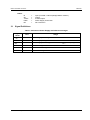
1
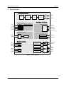
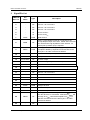
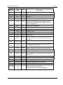
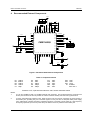
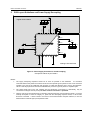
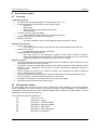
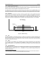
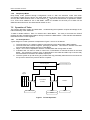
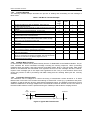
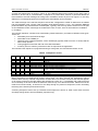
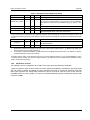
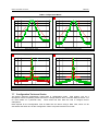
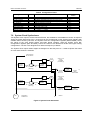
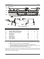
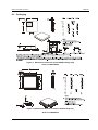
CML Microcircuits CMX7045 COMMUNICATION SEMICONDUCTORS AIS SART Processor D/7045FI-1.x/1 October 2011 Advance Information DATASHEET 7045FI-1.x Marine AIS SART Processor Features: Tx AIS GMSK Modem Conforms to IEC 61097-14 AIS SART Formatted Data Integration Roadmap Battery Monitor Low-Power (3.0V to 3.6V) Operation Flexible Tx Interface Low Profile 48-pin LQFP or VQFN Configurable by Function Image™ Two Auxiliary Clock Generators Two-Input Auxiliary (10-bit) ADC Four Auxiliary (10-bit) DACs Applications: PLL RTC C-BUS VCO PA Automatic Identification System (AIS) Search And Rescue (SART) for Marine Safety GPS Switched mode PSU PA Ramp Ref Osc µC CMX7045 SART Processor Monitor SART Test Battery This document contains: SART Active Tx Enable GPS Lock Slot Clock 1 Datasheet User Manual Strobe Brief Description The CMX7045 is a dedicated processor for marine Automatic Identification System (AIS), Search and Rescue Transmitter (SART) operation, fully meeting the requirements of IEC 61097-14. This highly integrated and flexible device includes a 9600 baud GMSK modem for transmission of formatted data. Additional auxiliary functions are also provided to further support the system host, these include: a two-input 10-bit ADC, four 10-bit DACs, two system clock outputs and four GPIOs. The CMX7045 offers low power sleep modes to ensure maximum system battery life and is available in a in a small 48-pin LQFP or VQFN package. This Datasheet is the first part of a two-part document comprising Datasheet and User Manual: the User Manual can be obtained by registering your interest in this product with your local CML representative. 2011 CML Microsystems Plc Marine AIS SART Processor CMX7045 CONTENTS 1 Brief Description ............................................................................................................................... 1 1.1 History........................................................................................................................................ 3 2 Block Diagram ................................................................................................................................... 4 3 Signal/Pin List.................................................................................................................................... 5 3.1 Signal Definitions ....................................................................................................................... 7 4 Recommended External Components ............................................................................................ 8 5 PCB Layout Guidelines and Power Supply Decoupling ............................................................... 9 6 General Description ........................................................................................................................ 10 6.1 Overview .................................................................................................................................. 10 6.2 AIS System Formats ................................................................................................................ 10 7 Detailed Description ....................................................................................................................... 11 7.1 Clock Source ........................................................................................................................... 11 7.2 Host Interface .......................................................................................................................... 11 7.3 Function Image™ Load and Activation ................................................................................... 12 7.3.1 FI Loading from Host Controller ................................................................................... 12 7.4 System Description and Tasks ................................................................................................ 14 7.4.1 Signal Routing.............................................................................................................. 14 7.4.2 Operating Modes ......................................................................................................... 14 7.4.3 Modem and Data Units ................................................................................................ 14 7.4.4 Timing and Synchronisation ........................................................................................ 15 7.4.5 Tx Timing ..................................................................................................................... 15 7.4.6 ADC ............................................................................................................................. 15 7.4.7 DACs ............................................................................................................................ 15 7.4.8 Interrupt Operation ....................................................................................................... 15 7.4.9 Deep Sleep Mode ........................................................................................................ 16 7.5 Operation of Tasks .................................................................................................................. 16 7.5.1 Tx Task Operation ....................................................................................................... 16 7.5.2 Registers and Buffers for Tx Tasks ............................................................................. 17 7.5.3 Write Data Registers .................................................................................................... 17 7.5.4 Data Tasks ................................................................................................................... 17 7.5.5 Modem Tasks and Codes ............................................................................................ 18 7.6 Transmission Format ............................................................................................................... 18 7.6.1 Transmit Tasks ............................................................................................................ 19 7.6.2 AIS Burst Mode Transmit ............................................................................................. 19 7.6.3 Transmit Example ........................................................................................................ 20 7.6.4 AIS Raw Mode Transmit .............................................................................................. 20 7.6.5 Transmitter Timing Control .......................................................................................... 20 7.6.6 Modulation Formats ..................................................................................................... 22 7.7 Configuration Tasks and Codes .............................................................................................. 23 7.8 System Clock Synthesisers ..................................................................................................... 24 7.9 Powersave ............................................................................................................................... 25 7.10 C-BUS Register Summary....................................................................................................... 26 8 Performance Specification ............................................................................................................. 27 8.1 Electrical Performance ............................................................................................................ 27 8.1.1 Absolute Maximum Ratings ......................................................................................... 27 8.1.2 Operating Limits ........................................................................................................... 27 8.1.3 Operating Characteristics ............................................................................................ 28 2011 CML Microsystems Plc 2 D/7045FI-1.x/1 Marine AIS SART Processor 8.2 8.3 CMX7045 8.1.4 Parametric Performance .............................................................................................. 31 C-BUS Timing .......................................................................................................................... 32 Packaging ................................................................................................................................ 33 TABLES Table 1 Definition of Power Supply and Reference Voltages ...................................................................... 7 Table 2 Component Values.......................................................................................................................... 8 Table 3 Data Tasks .................................................................................................................................... 18 Table 4 Modem Tasks................................................................................................................................ 18 Table 5 AIS Burst Transmit Example ......................................................................................................... 20 Table 6 Tx Sequence events ..................................................................................................................... 21 Table 7 Example Tx Event Sequence Setup ............................................................................................. 22 Table 8 Tx Spectrum Masks ...................................................................................................................... 23 Table 9 Configuration Tasks ...................................................................................................................... 24 Table 10 C-BUS Registers ......................................................................................................................... 26 FIGURES Figure 1 Block Diagram ................................................................................................................................ 4 Figure 2 Recommended External Components ........................................................................................... 8 Figure 3 Power Supply Connections and De-coupling ................................................................................ 9 Figure 4 C-BUS Transactions .................................................................................................................... 11 Figure 5 FI Loading from Host ................................................................................................................... 13 Figure 6 Tx Burst Timing ............................................................................................................................ 15 Figure 7 Tx Task Operation ....................................................................................................................... 16 Figure 8 Typical AIS Transmission ............................................................................................................ 20 Figure 9 System Clock Generation ............................................................................................................ 24 Figure 10 C-BUS Timing ............................................................................................................................ 32 Figure 11 Mechanical Outline for 48-pad VQFN Package (Q3) ................................................................ 33 Figure 12 Mechanical Outline for 48-pin LQFP Package (L4) ................................................................... 33 It is always recommended that you check for the latest product datasheet version from the Datasheets page of the CML website: [www.cmlmicro.com]. 1.1 History Version 1 Changes Date Initial release Oct 2011 2011 CML Microsystems Plc 3 D/7045FI-1.x/1 Marine AIS SART Processor 2 CMX7045 Block Diagram Transmit Functions HDLC Encode Buffer NRZI Encode DAC 1 DAC2 DAC 2 DAC3 DAC 3 DAC4 DAC 4 MOD2 Auxiliary Functions Auxiliary 10-bit DACs DAC1 MOD1 GMSK Modulation Configurable GPIO Ramp Profile RAM TXENA GPIO SLOTCLK CS-SYNC SLTCLKOP Multiplexed 10-bit ADC ADC1 ADC2 MUX Programmable System Clocks System Control System Clock 2 SYSCLK2 Crystal Oscillator Bias AVSS Registers DVDD Power Control VDEC SYSCLK1 Main Clock Digital PLL AVDD VBIAS System Clock 1 ADC Reg Internal Systems Control DVSS C-BUS Interface XTAL/CLK XTALN IRQN RDATA CSN CDATA SCLK Figure 1 Block Diagram 2011 CML Microsystems Plc 4 D/7045FI-1.x/1 Marine AIS SART Processor 3 CMX7045 Signal/Pin List CMX7045 Q3 or L4 Pin Name Type 1 - NC reserved – do not connect. 2 - NC reserved – do not connect. 3 - NC reserved – do not connect. 4 - NC reserved – do not connect. 5 - IP Connect to DVDD. 6 - IP Connect to DVDD. 7 DVSS PWR Description Digital Ground. C-BUS: A 'wire-ORable' output for connection to the Interrupt Request input of the host. Pulled down to DVSS when active and is high impedance when inactive. An external pull-up resistor (R1) is required. 8 IRQN OP 9 VDEC PWR 10 SLOTCLK IP Slot clock from host (37.5Hz). 11 CS-SYNC OP Slot Sync. 12 SLTCLKOP OP Slot clock output. 13 SYSCLK1 OP Synthesised Digital System Clock Output 1. 14 DVSS PWR 15 TXENA OP Enable for external Tx hardware. 16 - NC reserved – do not connect. 17 - NC reserved – do not connect. 18 - NC reserved – do not connect. 19 - NC reserved – do not connect. 20 - NC reserved – do not connect. 21 - NC reserved – do not connect. 22 AVSS PWR Analogue Ground. 23 MOD1 OP Modulator 1 output. 24 MOD2 OP Modulator 2 output. Internally generated 2.5V digital supply voltage. Must be decoupled to DVSS by capacitors mounted close to the device pins. No other connections allowed. Digital Ground. 25 VBIAS OP Internally generated bias voltage of about AVDD/2, except when the device is in ‘Powersave’ mode when VBIAS will discharge to AVSS. Must be decoupled to AVSS by a capacitor mounted close to the device pins. No other connections allowed. 26 - NC reserved– do not connect this pin. 2011 CML Microsystems Plc 5 D/7045FI-1.x/1 Marine AIS SART Processor CMX7045 CMX7045 Q3 or L4 Pin Name Type 27 - NC reserved– do not connect. 28 - NC reserved – do not connect. 29 ADC1 IP ADC input 1. 30 ADC2 IP ADC input 2. Description Analogue +3.3V supply rail. Levels and thresholds within the device are proportional to this voltage. This pin should be decoupled to AVSS by capacitors mounted close to the device pins. 31 AVDD PWR 32 DAC1 OP Aux DAC output 1/RAMDAC. 33 DAC2 OP Aux DAC output 2. 34 AVSS PWR Analogue Ground. 35 DAC3 OP Aux DAC output 3. 36 DAC4 OP Aux DAC output 4. 37 DVSS PWR Digital Ground. 38 VDEC PWR Internally generated 2.5V supply voltage. Must be decoupled to DVSS by capacitors mounted close to the device pins. 39 XTAL/CLK IP 19.2MHz input from the external clock source or 9.6MHz Xtal. 40 XTALN OP The output of the on-chip 9.6MHz Xtal oscillator inverter. NC if 19.2MHz clock is used. 41 DVDD PWR Digital +3.3V supply rail. This pin should be decoupled to DVSS by capacitors mounted close to the device pins. 42 CDATA IP 43 RDATA 44 - NC 45 DVSS PWR 46 SCLK IP C-BUS: The C-BUS serial clock input from the µC. 47 SYSCLK2 OP Synthesised Digital System Clock Output 2. 48 CSN IP C-BUS: The C-BUS chip select input from the µC. ~ The central metal pad may be connected to Analogue Ground (AVSS) or left unconnected. No other electrical connection is permitted. EXPOSED METAL PAD SUB 2011 CML Microsystems Plc C-BUS: Command Data. Serial data input from the µC. C-BUS: Reply Data. A 3-state C-BUS serial data output to TS OP the µC. This output is high impedance when not sending data to the µC. reserved – do not connect this pin. Digital Ground. 6 D/7045FI-1.x/1 Marine AIS SART Processor CMX7045 Notes: IP OP TS OP PWR NC 3.1 = = = = = Input (+PU/PD = internal pullup/pulldown resistor) Output 3-state Output Power Supply Connection No Connection Signal Definitions Table 1 Definition of Power Supply and Reference Voltages Signal Name Pins Usage AVDD AVDD Power supply for analogue circuits. DVDD DVDD Power supply for digital circuits. VDEC VDEC Power supply for core logic, derived from DVDD by on-chip regulator. VBIAS VBIAS Internal analogue reference level, derived from AVDD. AVSS AVSS Ground for all analogue circuits. DVSS DVSS Ground for all digital circuits. 2011 CML Microsystems Plc 7 D/7045FI-1.x/1 Marine AIS SART Processor 4 CMX7045 Recommended External Components DVDD + C20 C21 C22 C1 DVSS SLOTCLK CS-SYNC SLTCLKOP 31 30 8 29 9 28 10 27 11 26 12 25 13 14 15 16 17 18 19 20 21 22 23 24 SYSCLK1 DVSS DVSS CMX7045Q3 7 MOD2 C23 VDEC 32 MOD1 C24 XTALN 5 AVSS + DVDD 33 NC VDEC CDATA 4 TXENA IRQN RDATA 34 DVSS DVSS NC 3 6 DVSS DVSS SCLK 35 NC NC 2 NC NC DVSS 36 NC R2 C3 1 NC R1 NC C2 48 47 46 45 44 43 42 41 40 39 38 37 NC NC DVDD SYSCLK2 CSN DVSS XTAL/CLK X1 AUXDAC4 AUXDAC3 AVSS AUXDAC2 AVSS AUXDAC1 AVDD AVDD AUXADC2 + C17 C18 C19 AUXADC1 NC AVSS NC NC VBIAS C7 AVSS R3 C8 DVSS R4 AVSS AVSS C9 AVSS Figure 2 Recommended External Components Table 2 Component Values R1 R2 R3 R4 C1 100k 220k 100k 100k 18pF C2 C3 C7 C8 C9 18pF 10nF 100nF 100pF 100pF C17 C18 C19 C20 C21 10µF 10nF 10nF 10µF 10nF C22 C23 C24 X1 10nF 10nF 10µF 9.6MHz See note 1 Resistors 5%, capacitors and inductors 20% unless otherwise stated. Notes: 1. X1 can be a 9.6MHz crystal or a 19.2MHz external clock generator. The tracks between the crystal and the device pins should be as short as possible to achieve maximum stability and best start up performance. 2. A single 10µF electrolytic capacitor (C24, fitted as shown) may be used for smoothing the power supply to both VDEC pins, providing they are connected together on the pcb with an adequate width power supply trace. Alternatively, separate smoothing capacitors should be connected to each VDEC pin. High frequency decoupling capacitors (C3 and C23) must always be fitted as close as possible to both VDEC pins. 2011 CML Microsystems Plc 8 D/7045FI-1.x/1 Marine AIS SART Processor 5 CMX7045 PCB Layout Guidelines and Power Supply Decoupling DVDD Digital Ground Plane + C20 C21 C22 DVSS DVSS DVSS VDEC DVSS DVDD C3 DVSS 48 47 46 45 44 43 42 41 40 39 38 37 1 36 2 35 3 34 4 33 5 32 CMX7045Q3 6 DVSS DVSS VDEC C23 DVSS 8 29 9 28 10 27 11 26 12 25 13 14 15 16 17 18 19 20 21 22 23 24 AVSS C24 31 AVSS DVSS AVSS AVDD AVDD + 30 DVSS + 7 AVSS C17 C18 C19 AVSS VBIAS C7 AVSS Analogue Ground Plane Figure 3 Power Supply Connections and De-coupling Component values as per Table 2. Notes: 1. The supply decoupling capacitors should be as close as possible to the CMX7045. It is therefore recommended that the printed circuit board is laid out with separate ground planes for the AV SS and DVSS supplies in the area of the CMX7045, with provision to make links between them, close to the CMX7045. Use of a multi-layer printed circuit board will facilitate the provision of ground planes on separate layers. 2. The central metal pad on the ‘Q3’ package may be electrically unconnected or, alternatively, may be connected to Analogue Ground (AVSS). No other electrical connection is permitted. 3. VBIAS is used as an internal reference for detecting and generating the various analogue signals. It must be carefully decoupled to ensure its integrity so, apart from the decoupling capacitor shown, no other loads should be connected. If VBIAS needs to be used to set the discriminator mid-point reference, it must be buffered with an external high input impedance buffer. 2011 CML Microsystems Plc 9 D/7045FI-1.x/1 Marine AIS SART Processor 6 6.1 CMX7045 General Description Overview Tx Modem Functions AIS 25kHz channel (GMSK, 9600bps, 2.4kHz deviation, BT = 0.4) AIS Burst mode with full AIS frame formatting (HDLC-type) o Bit stuffing o NRZI coding o Training sequence and start/stop flag insertion o CRC generation AIS Raw mode (for greater flexibility) o Supports arbitrary data streams for user-defined protocols 160-byte (equivalent to 5 AIS slots) Tx data buffer Flexible Tx Interface o Two-point modulation outputs, with independent gain and polarity controls Analogue I/O Functions Auxiliary ADC system o A two-input 10-bit successive approximation ADC with integrated sample and hold Auxiliary DAC system o Four general purpose auxiliary 10-bit DACs Ramping auxiliary DAC (using DAC 1) o DAC steps through a user-configured sequence of DAC output values to develop a specific rising/falling DAC output signal. This is useful for ramping an RF PA, and can be configured to operate automatically at the start and end of a burst. System Functions All internal subsystems are controlled via a single serial host interface to reduce host µC pin count and simplify external host driver complexity. Transaction oriented command/response logical host interface executes tasks supporting normal operation, device configuration, and functions to assist manufacturing calibration trimming of external circuits. Internal system clock derived from reference oscillator and eliminates the need for additional XTAL or baseband clock oscillator. Auxiliary clock synthesisers generate two clocks for external use to support peripheral devices. Function Image™ is loaded directly from the host µC via C-BUS. Integrated 2.5V regulator can develop 2.5V from required 3.3V supply. Powersave facilities minimise total system power. 6.2 AIS System Formats The AIS system uses two basic channel access mechanisms: Self Organising Time Division Multiple Access (SOTDMA) and Carrier-Sensing Time Division Multiple Access (CSTDMA). The CMX7045 is compatible with both systems and offers additional features which simplify the implementation of an AIS SART device conforming to IEC 61097-14. The relevant International standards are: [0] ITU-R M.1371-4 [1] IEC 61993-2 Class A [2] IEC 62287-1 Class B CSTDMA [3] IEC 62287-2 Class B SOTDMA [4] IEC 62320-1 Base Station [5] IEC 62320-2 Aids to Navigation [6] IEC 61097-14 AIS-SART 2011 CML Microsystems Plc 10 D/7045FI-1.x/1 Marine AIS SART Processor 7 CMX7045 Detailed Description 7.1 Clock Source The CMX7045 can be used with either a 9.6MHz xtal or a 19.2MHz oscillator. 7.2 Host Interface This section provides a general description of the C-BUS serial interface protocol used to transfer data, control and status information between the CMX7045 and its host. C-BUS is a serial interface, similar to SPI, that uses a simple transaction-oriented command/response protocol with addressing to access specific registers within the CMX7045. Each C-BUS transaction consists of a single Register Address/Command byte (A/C byte) sent from the µC which may be followed by one or more data byte(s) sent from the µC to be written into one of the CMX7045’s Write Only registers, or one or more data byte(s) read out from one of the CMX7045’s Read Only registers, as illustrated in Figure 4. Data sent from the µC on the CDATA line is clocked into the CMX7045 on the rising edge of the SCLK input. RDATA sent from the CMX7045 to the µC is valid when the SCLK is high. The CSN line must be held low during a data transfer and kept high between transfers. The C-BUS interface is compatible with most common µC serial interfaces and may also be easily implemented with general purpose µC I/O pins controlled by a simple software routine. The number of data bytes following an A/C byte is dependent on the value of the A/C byte. The most significant bit of the address or data is sent first. For detailed timings see section 8.2. C-BUS Write: See Note 1 See Note 2 CSN SCLK CDATA 7 6 5 4 3 2 1 MSB 0 7 LSB MSB Address / Command byte 6 … 0 7 LSB MSB Upper 8 bits … 0 LSB Lower 8 bits RDATA High Z state C-BUS Read: See Note 2 CSN SCLK CDATA 7 6 5 4 3 2 MSB 1 0 LSB Address byte Upper 8 bits RDATA 7 High Z state Data value unimportant 6 MSB Repeated cycles … Lower 8 bits 0 7 LSB MSB … 0 LSB Either logic level valid Figure 4 C-BUS Transactions Notes: 1. 2. 3. 4. 5. For Command byte transfers only the first 8 bits are transferred. For single byte data transfers only the first 8 bits of the data are transferred. The CDATA and RDATA lines are never active at the same time. The Address byte determines the data direction for each C-BUS transfer. The SCLK input can be high or low at the start and end of each C-BUS transaction. The gaps shown between each byte on the CDATA and RDATA lines in the above diagram are optional, the host may insert gaps or concatenate the data as required. 2011 CML Microsystems Plc 11 D/7045FI-1.x/1 Marine AIS SART Processor 7.3 CMX7045 Function Image™ Load and Activation The Function Image™ (FI) file, which defines the operational capabilities of the device, may be obtained from the CML Technical Portal, following registration. This is in the form of a 'C' header file which can be TM included into the host controller software. The Function Image data file is no more than 24kbytes. Once the FI has been loaded, the CMX7045 performs these actions: (1) (2) (3) (4) the product identification code ($7045) is reported in C-BUS register $C5 the FI version code is reported in C-BUS register $C9 the two 32-bit FI checksums are reported in C-BUS register pairs $A9, $AA and $B8, $B9 the device waits for the host to load the 32-bit Device Activation Code to C-BUS register $C8 (5) once activated, the device initialises fully, enters Deep Sleep mode mode and becomes ready for use, and the Activation Register Ready (ACT) flag (bit 0 of the Status register) will be set (6) Once the Deep Sleep bit (Status2 b:13) has been set, the host may then power down the Analogue sections of the device to minimise power consumption (typically while the host is waiting for the external GPS to output a valid position fix) (7) When the host decides that the device should be returned to active mode in order to configure the device or transmit an AIS burst, it should first power-up the Analogue sections and then send the “exit Deep Sleep” command. The checksums should be verified against the published values to ensure that the FI has loaded correctly. Once the FI has been activated, the checksum, product identification and version code registers are cleared and these values are no longer available. If an invalid activation code is loaded, the device will report the value $DEAD in register $A9 and become unresponsive to all further host commands (including General Reset). A power-on reset is required to recover from this state. Both the Device Activation Code and the checksum values are available from the CML Technical Portal. Following a General Reset, reloading of the FI is required. 7.3.1 FI Loading from Host Controller The FI needs to be included into the host controller software build and downloaded into the CMX7045 at power-up over the C-BUS interface. Wait for the ACT flag to be set (Status register $C6 bit 0), then the data can then be sent directly over the C-BUS to the CMX7045. Each time the device is powered up or reset, its FI must first be loaded and then activated. These two steps assign internal device resources and determine all device features. The device does not operate until the FI is loaded and activated. The download time is limited by the clock frequency of the C-BUS, with a 5MHz SCLK, it should take less than 500ms to complete. 2011 CML Microsystems Plc 12 D/7045FI-1.x/1 Marine AIS SART Processor CMX7045 Power-up or write General Reset to CMX7032/CMX7042 Poll $C6 until b0 = 1 (ACT flag set) Configure ACT flag interrupt, if required Write Start Block 1 Address (DB1_ptr) to $B6 Write Block 1 Length (DB1_len) to $B7 Write $0001 to $C8 Wait for ACT flag to go high or interrupt Write next data word to $C8 Wait for ACT flag to go high or interrupt Write Start Block 2 Address (DB2_ptr) to $B6 Write Block 2 Length (DB2_len) to $B7 Write $0001 to $C8 Wait for ACT flag to go high or interrupt Write next data word to $C8 Wait for ACT flag to go high or interrupt Write Start Block 3 Address (ACTIVATE_ptr) to $B6 Write Block 3 Length (ACTIVATE_len) to $B7 Write $0001 to $C8 Wait for ACT flag to go high or interrupt Read and verify checksum values in register pair: $A9 and $AA, $B8 and $B9 Send Activation Code hi to $C8 Wait for ACT flag to go high or interrupt Send Activation Code lo to $C8 Wait for ACT flag to go high or interrupt CMX7045 is now ready for use Figure 5 FI Loading from Host 2011 CML Microsystems Plc 13 D/7045FI-1.x/1 Marine AIS SART Processor 7.4 CMX7045 System Description and Tasks This section describes the operation of main sections of the CMX7045 and the task-oriented logical interface provided to the external host device. 7.4.1 Signal Routing The Tx Modulation output signals may be configured to be suitable for two-point modulation circuits. Signal levels on both output pins, MOD1 and MOD2, can be set to within 0.2dB using a Configuration Mode task. 7.4.2 Operating Modes The CMX7045 operates in either: o Deep Sleep Mode o Configuration mode o Normal mode Deep Sleep mode puts the device into a low-power standby mode to minimize power consumption. Whilst in this mode the host can switch off un-needed analogue functionality. Once the device has been activated, it will enter deep sleep mode automatically. Configuration mode is used to set up various operating parameters of the CMX7045 subsystems, e.g. Transmit format, timing parameters etc. following a power-up or reset. The modem section is disabled when the device is in Configuration mode. Configuration mode uses dedicated tasks that are not valid whilst in Normal mode. Normal mode is used when actively running the CMX7045 modem and other subsystems. Normal mode uses dedicated tasks that are not valid whilst in Configuration mode. “Enter Config Mode” (ECM) is a Normal mode task that switches the device from Normal to Configuration mode. “Exit Config Mode” (EXIT_CONFIG) is a Configuration mode task that switches the device from Configuration to Normal mode. 7.4.3 Modem and Data Units The CMX7045 is logically divided into two main units which can accept and perform tasks separately: o Modem Unit o Data Unit The Modem Unit is primarily responsible for processing Tx data from the internal Tx data buffer, presenting it on the MOD1 and MOD2 pins. The Data Unit is primarily responsible for transferring data between the internal data buffers or subsystems and the C-BUS registers, from where they can be accessed by the host µC. When the device is in Normal mode, the Command register, $C8, is a 16 bit C-BUS write register that contains task fields for both Data and Modem units. A task is invoked by writing its code into the Data Task or Modem Task fields. A single C-BUS write transaction will change all Command register fields. Often, the host will only want to issue either a Data or Modem task, in which case it should ensure that the other task field is set to all zeroes, corresponding to a null/idle task. Sometimes it is useful to issue Data and Modem tasks simultaneously, in which case, the Data task will always be completed before the Modem task is started. Certain internal subsystems can be directly accessed and controlled via C-BUS transactions, without issuing a specific task/command. 2011 CML Microsystems Plc 14 D/7045FI-1.x/1 Marine AIS SART Processor CMX7045 7.4.4 Timing and Synchronisation The CMX7045 requires a Slot Clock (SLOTCLK) input from the host µC. This should be a pulse at least 50µs long, whose rising edge is aligned to the AIS Slot boundary. An edge is required at the start of every AIS slot or frame, hence the frequency of this signal is 37.5Hz or 0.5Hz1. The CMX7045 has several features to assist the host µC with timing, which are detailed below. All of these features are based on the SLOTCLK signal, provided by the host to the CMX7045’s SLOTCLK pin. All timings are defined as a number of 24kHz “ticks” referenced to the rising edge of the SLOTCLK signal. 7.4.5 Tx Timing The CMX7045 can be configured to perform a sequence of events when a TXB or TDBS task (transmit burst) is issued. The events are: start and end of modulation, ramping the RAMDAC up and down, asserting and releasing a digital output pin (intended as a Tx Enable) and CSTDMA sensing. Each of these can be configured to happen with specified delays from the rising edge of the SLOTCLK. The timings are set up with the Config Mode task Tx_Sequence. See User Manual section 9.12.3 for details. Tx Timing SlotCLK Tx Enable SlotCLK PA Ramp & Modulation Time Figure 6 Tx Burst Timing 7.4.6 ADC The ADC is available for user defined functions. The ADC runs continuously, the input is selected by the ADC Input Select bits in the C-BUS Mode register, $C1 and the results of the conversion are presented in ADC Data C-BUS register $C9. This register also includes a bit field to indicate which input was selected when this conversion was executed. 7.4.7 DACs The four DACs can be updated in any combination using the DAC_Write data task. See User Manual 9.12. In addition, DAC1 can be configured as a RAMDAC to output a series of values as part of the transmit timing sequence. The values and the rate at which they change are set-up using a Config mode task. 7.4.8 Interrupt Operation The CMX7045 will issue an interrupt on the IRQN line when the IRQ bit (bit 15) of the Status register and the IRQ Mask bit (bit 15) are both set to 1. User Manual section 9.14 describes the situations which cause the IRQ bit to change from a 0 to a 1. The IRQN pin is an open collector output that requires an external pull-up resistor. 1 If the host supplies a 0.5Hz signal, this should be aligned to the even UTC second and the selection of X1 should be chosen to maintain correct timing between SLOTCLK pulses. 2011 CML Microsystems Plc 15 D/7045FI-1.x/1 Marine AIS SART Processor CMX7045 7.4.9 Deep Sleep Mode Deep Sleep mode (entered through Configuration mode or after the activation codes have been successfully loaded) puts the device into static state where all signal processing and clocks are stopped and only the C-BUS remains active. In this mode, the I DD drops to the lowest level, as specified in section 8.1.3, and is thus suitable for use in AIS SART, where it is feasible for the host µC to switch off the CMX7045 at known times. See User Manual section 9.12.6. 7.5 Operation of Tasks This section describes modem and data tasks. Understanding their operation requires knowledge of the internal buffering of the CMX7045. Tx data is double buffered. Each Tx channel has a Data Buffer. The host µC accesses the C-BUS registers and the modulator/demodulator directly accesses the Data Buffers. Tasks transfer data between the buffers and the C-BUS registers. 7.5.1 Tx Task Operation Typical stages of Tx task operation are depicted in Figure 7 and occur as follows: 1. The host writes up to 4 words of data for transmission into the Write Data C-BUS registers. 2. The host writes the Command register, specifying a data task. This results in transfer of the data from the Write Data registers into the Tx Data Buffer. 3. Steps 1 and 2 can be repeated to load the Tx Data Buffer with a large block of data. 4. A Modem task can then be used to instruct the Tx Modulator to transmit the data in the Data Buffer. This causes the content of the Tx Data Buffer to be coded and CRC’d (if in burst mode) and transmitted to the MOD1 and MOD2 output pins. 5. Once the system is up and running any modem task may potentially take some time to execute as it may have to wait for the previous task to complete. Command Register Data Task Command Reg Free Modem Task C-Bus registers B 7 B 6 A 8 A 7 Tx Data Buffer (88 words) Data Task Complete Modulator TBFree TxState TxDone Figure 7 Tx Task Operation 2011 CML Microsystems Plc 16 D/7045FI-1.x/1 Marine AIS SART Processor 7.5.2 CMX7045 Registers and Buffers for Tx Tasks Command register: contains Data and Modem task fields as described above. Status register: contains bits that indicate when tasks are complete, which can interrupt the host: o Command Reg Free o TBFREE o TxDONE o Config Task Complete o Data Task Complete. Interrupt Mask: Host write register to specify which status bit can cause an interrupt. Write Data registers 0-3: Contain data written from host µC to transmit via the Tx Modulator. Tx Data Buffer: The Tx Data is double buffered, which allows the host µC to write to the Tx Data Buffer while the modulator is simultaneously transmitting data it reads from the Tx Modem Buffer. Each buffer is capable of holding one full (5-slot) AIS message. 7.5.3 Write Data Registers An array of four, 16 bit, C-BUS write registers form the Write Data C-BUS registers. The device reads and acts upon the content of these data write registers as instructed by the Data Task bits of the Command register while in transmit mode. Generally, they may be written at any time by the host µC with no effect on internal device operation. When a “Data task” is issued the Data registers will be read by the device and so should not be modified by the host µC until the Data Task complete bit is set in the Status register. Data tasks access the registers as a number of words (1 to 4) or as a number of bits (1 to 16 in $A7), however if a bit-format Data Task is used it must be the final data task issued in a multi-data transfer from the host. The next data task issued should be a DataWordResetN_Tx or DataBitResetN_Tx to re-initialise the internal data buffer pointers (a bit-format task is usually used as the last transfer of a data block that is not a complete number of words in length). Word-format: Bit: Register $A7 Bit: Register $A8 Bit: Register $B6 Bit: Register $B7 15 14 13 15 14 13 15 14 13 15 14 13 15 14 13 12 11 10 9 8 7 6 5 4 Data write from host µC to device word 1(MSB sent first) 12 11 10 9 8 7 6 5 4 Data write from host µC to device word 2(MSB sent first) 12 11 10 9 8 7 6 5 4 Data write from host µC to device word 3(MSB sent first) 12 11 10 9 8 7 6 5 4 Data write from host µC to device word 4(MSB sent first) 3 2 1 0 3 2 1 0 3 2 1 0 3 2 1 0 2 1 0 Bit-format: Bit: Register $A7 12 11 10 9 8 7 6 5 4 3 Data write from host µC to device bits 0-15, (bit 15 transmitted first) 7.5.4 Data Tasks Data tasks are used to: Load data from the Write Data registers into Data Buffers while in normal or configuration modes Load data from the Data Buffers to the DACs Write or operate subsystems by passing data using the Write Data registers. 2011 CML Microsystems Plc 17 D/7045FI-1.x/1 Marine AIS SART Processor CMX7045 Table 3 Data Tasks Name NULL DataWordResetN_Tx DataBitReadN_Rx1 DataBitReadN_Rx2 DataBitWriteN_Tx DataBitResetN_Tx DAC_Write Description Null system task – takes no action. Reset Tx data buffer pointer. Copy N words (1 to 4) from Write Data registers to Tx data buffer. Increment the data buffer pointer. Copy N bits (1 to 15) from Rx1 data buffer to Read Data register 0. Increment the data buffer pointer. Copy N bits (1 to 15) from Rx2 data buffer to Read Data register 0. Increment data buffer pointer. Copy N bits (1 to 15) from Write Data register 0 to Tx data buffer. Increment data buffer pointer. Reset Tx data buffer pointer. Copy N bits (1 to 15) from Write Data register 0 to Txdata buffer Increment data buffer pointer. Interprets each of the first 1 to 4 words in the Write Data registers as a write command for the Auxiliary DACs. 7.5.5 Modem Tasks and Codes Modem tasks transmit data on the MOD1 and MOD2 output pins. Modem tasks also coordinate data transfer between the Data Buffer and the modem. Note that for receive tasks a 1 or 2 at the end of the task name refers to the Rx channel which is being addressed. Table 4 Modem Tasks Name NULL AbortTx ECM Tx Tasks Tx Raw bit = 0 TXB Description No command – takes no action Enter Configuration mode Code and transmit AIS message using contents of data buffer. Start on next SLOTCLK Tx Raw bit = 1 TDBS TDB PRBS TRW HCT 7.6 Transmit contents of data buffer. Start on next SLOTCLK Transmit N data bits from the Tx mod buffer. Start as soon as modulator is free Transmit pseudorandom bit sequence Repeatedly transmit one word Hardware Control Transmission Format The CMX7045 is capable of transmitting AIS data in either raw mode or burst mode. In AIS raw mode, data is passed directly from the Tx Data Buffer to the GMSK modulator, so the µC will be responsible for sending any necessary training sequences and performing HDLC processing and NRZI coding. In AIS burst mode, the CMX7045 uses an internal message buffer to assemble an entire message (up to 5 slots) to which it automatically adds the training sequence, start/stop flags, CRC, bit stuffing and NRZI coding prior to transmission. After setting up the appropriate registers, transmission is initiated by issuing a Tx Burst or Tx Raw task. 2011 CML Microsystems Plc 18 D/7045FI-1.x/1 Marine AIS SART Processor 7.6.1 CMX7045 Transmit Tasks AbortTx: This causes the current task on the Tx channel to abort. It also clears the Tx modem buffer. TXB: Transmit AIS Burst This task can only be executed if the Tx Raw bit (bit 5 in the command register) is cleared to 0. This causes the CMX7045 to take the contents of the Tx Data buffer, apply AIS data coding and transmit the resulting AIS message. The transmit sequence will start on the next SLOTCLK edge. The following five transmit tasks can only be executed if the Tx Raw bit is set to 1: TDBS: Transmit Data Buffer on SLOTCLK This causes the CMX7045 to transmit the data buffer contents using AIS modulation. No data coding is applied, the Transmit Sequence will start on the next SLOTCLK edge, at which point the CS-SYNC output will become active. TDB: Transmit Data Buffer This causes the CMX7045 to transmit the data buffer contents using AIS modulation. No data coding is applied. The data will be transmitted as the modulator is available (Transmit Sequence is ignored). PRBS: Transmit Pseudorandom Bit Sequence This task causes the CMX7045 to transmit an internally generated pseudorandom bit sequence. The sequence is 511 bits in length, but will repeat indefinitely until aborted using the AbortTx task, (Transmit Sequence is ignored). TRW: Transmit Repeated Word This task causes the CMX7045 to repeatedly transmit the first word currently in the data buffer. Transmission will start immediately and will continue until an Abort Tx task is issued, (Transmit Sequence is ignored). HCT: Hardware Control Task Allows manual control of ancillary hardware functions. 7.6.2 AIS Burst Mode Transmit In AIS burst mode, the CMX7045 responds to a TXB task by performing bit stuffing, NRZI encoding and the addition of training sequence, start/stop flags and CRC checksum as required by AIS. Note: in AIS burst mode, the data words are automatically transmitted least significant bit first as required by the AIS specification. A number of error conditions are checked for during AIS burst mode transmit, each of which causes transmission to be aborted and a Tx Done interrupt to be generated. The associated Tx states are: Tx Aborted, message too long: This occurs if the internal message buffer is not big enough for the HDLC coded data (should not happen in normal operation, as the message buffer is big enough for a 5-slot message). This condition requires the µC to issue a AbortTx task. Tx Aborted, buffer not ready: This occurs in burst mode if the internal data coding has not completed before the timing_start value expires. 2011 CML Microsystems Plc 19 D/7045FI-1.x/1 Marine AIS SART Processor CMX7045 7.6.3 Transmit Example The following detailed example describes the process of loading and transmitting an AIS message in Burst mode. Table 5 AIS Burst Transmit Example Description 1. The host should ensure that the TBFREE, Data Task and CmdReg Free bits are set. 2. The host loads the first N(typically 4) data words into the write data registers. 3. The host issues a DataWordResetN_Tx Data Task. 4. Device reads the Command register & notes task types. 5. Device carries out the data task by copying the N data words as the first N data words of the data buffer. 6. The steps above may be repeated (Using DataWordWriteN_Tx tasks) to load many words until the data buffer contains enough data to carry out the desired modem task. 7. The host writes a TXB task to the Command register to start the Tx process. 8. Device reads the Command register. 9. Device codes the data. Tx state changes from Idle to Tx Pending 10. When the transmit point arrives (SLOTCLK), the Tx State changes to Tx in progress and the TxSequence is activated. 11. The Tx Modem Buffer will gradually empty as the Tx Modulator continues transmitting. 12. When the transmission ends the TxDone bit in the Status register will be set, generating an interrupt if enabled. The host should then check the Tx state bits in the Status2 register to see if transmission was successful. Cmd Reg Free 1 Data Task TBFREE TxDONE 1 1 1 1 1 1 1 0 1 1 1 0 1 1 1 1 1 1 1 0 1 1 1 1 1 1 1 0 1 1 0 1 1 1 1 1 1 1 1 7.6.4 AIS Raw Mode Transmit In AIS raw mode, transmit data is passed directly from the Tx Data Buffer to the GMSK modulator. The µC must calculate the entire transmitted message including the training sequence, HDLC processing (start/stop flags, bit stuffing, and CRC insertion) and NRZI coding. Note: In AIS raw mode, data words written to the CMX7045 are transmitted most significant bit first. The AIS message structure, however, requires each message byte to be output least significant bit first. The µC must therefore ensure that during the process of HDLC processing and NRZI coding that the resulting data bytes are correctly reversed. 7.6.5 Transmitter Timing Control The CMX7045 can be configured to control the timing of transmission events whenever a Tx Burst Modem task is executed. This includes the enabling of external RF circuits (e.g. synthesisers and power amplifier), as well as the time at which internal data modulation begins. The flexibility of this timing control allows the CMX7045 to be simply adapted to the characteristics of the RF transmit circuits. The control of the external RF transmit circuits is performed using the TXENA pin and the DAC1 ramping function. RF Power SLOTCLK 100% SLOTCLK Modulation B Time Figure 8 Typical AIS Transmission 2011 CML Microsystems Plc 20 D/7045FI-1.x/1 Marine AIS SART Processor CMX7045 A typical AIS transmission is shown in Figure 8. The CMX7045 starts timing relative to the rising edge of SLOTCLK. At the end of a transmission, a sequence of “power-down” actions is performed which are timed relative to the last message bit having been modulated, shown as point B in Figure 8. In this way differences in message length due to bit stuffing are automatically accommodated. The relative timings of the transmit sequence events are configured as a table of values that are loaded into the CMX7045 using a Config Task operation (User Manual section 9.12.3) – this operation must be performed before any transmissions are attempted. Typically, this will only need to be done once as part of an initialization routine. All timings are measured in units of “ticks”, each of which lasts for 1/24000Hz ( 41.666µs). The transmit sequence consists of two initial setting values followed by a number of different event types. These are: Initial delay from the SLOTCLK edge Initial state of the TXENA pin Changes to the external hardware, via the TXENA pin (typically used to turn the Tx on/off) and the DAC1 ramp up/down Timing triggers for the start and end of the data modulation A dummy event in case any of the above are not required in the application. The transmit event sequence is programmed using a Config task, see User Manual section 9.12.3. Table 6 Tx Sequence events b3 b2 b1 b0 Event id Description 0 0 0 0 0 0 0 0 0 0 0 1 1 1 0 0 1 1 0 0 1 0 1 0 1 0 1 0 dummy Tx_en_hi RAMDAC_UP MODULATE_START MODULATE_END 0 1 1 1 0 0 1 0 0 1 0 1 RAMDAC_DOWN Tx_en_lo dummy Do nothing reserved reserved Pin TXENA is set high AuxDAC1 will start executing a Ramp up Defines the start of data modulation Delay from the end of modulation (based on the last data bit loaded into modem - includes a 20 tick delay for the internal filters) AuxDAC1 will start executing a Ramp down Pin TXENA is set low Do nothing When calculating the MODULATE_START timing value, the delay through the CMX7045’s internal transmit filters and any external components must be taken into account to ensure that data bits appear on-air at the correct time (the filter delays are specified in section 8.1.4. The MODULATE_END event has an in-built delay of 20 ticks to allow the last bit to make its way out of the transmit filter. Allowance must be made for this built-in delay, as well as for the delay through any external components, when calculating the timing of the transmit power down events. A working example of how to set up a transmit event sequence is shown in Table 7 (the order of events and delay timings shown are for illustrative purposes only): 2011 CML Microsystems Plc 21 D/7045FI-1.x/1 Marine AIS SART Processor CMX7045 Table 7 Example Tx Event Sequence Setup Parameter dummy Event ID Delay Total 0 0 Explanation 0 Do nothing MODULATE_START 5 1 1 Start feeding data to the transmit modulator and filters (this allows for the 20 tick storage delay in the Tx filters so that modulated data appears at the end of the RAMDAC ramp_up period – tick 57). dummy 0 0 0 Do nothing Tx_en_hi 3 0 1 Set TXENA line high RAMDAC_UP 4 3 4 Insert 3 tick delay then initiate the RAMDAC ramp-up (for AIS, the transmitted signal will be carrier only at this point) At this point during a transmission the CMX7045 feeds the entire message to the transmit modulator bit-by-bit. All subsequent transmit events are timed relative to the end of the last message bit, indicated by the MODULATE_END event. RAMDAC_DOWN 7 2 0 Initiate the RAMDAC ramp-down immediately Tx_en_lo 8 7 9 Insert 7 tick delay (to allow RAMDAC to fully ramp down) then set the TXENA line low. MODULATE_END 6 5 14 Allows for process delays Notes: 1. MODULATE_START must appear in the first group of timed events (table entries 1–5), MODULATE_END must appear in the final group (table entries 6-8). 2. It is feasible to place the RAMDAC_DOWN task before the MODULATE_END task if it is desired to continue modulation during the Ramp down period. Assuming that the timing_start value has been set to 0 (see User Manual section 9.12.3) and the RAMDAC is set to its default values (312us), this sequence approximates to the SART timing with ideal hardware (RAMDAC starts 5bits / 12 ticks after SLOTCLK). 7.6.6 Modulation Formats The CMX7045 can be configured to drive either a two-point VCO and Reference modulator. Typical Tx spectrum plots for both modes are shown below (generated by modulating a signal generator with the outputs of MOD1 and MOD2 and then analysing the signal on a spectrum analyser). Note that these plots represent the steady-state transmission and so are shown with the Class A and Class BSOTDMA spectrum mask (-70dBc). The Class B–CSTDMA standard specifies a slotted transmission with a mask at –60dBc. 2011 CML Microsystems Plc 22 D/7045FI-1.x/1 Marine AIS SART Processor CMX7045 Table 8 Tx Spectrum Masks Marker 1 [T1] Ref Lvl -1.88 dBm -1.9 dBm 161.97596192 MHz 1 RBW 1 kHz RF Att VBW 1 kHz Mixer SWT 150 ms 10 dB -20 dBm Unit RBW 1 kHz RF Att Ref Lvl VBW 1 kHz Mixer 0 dBm SWT dB 0 150 ms 20 dB -20 dBm Unit dBm 0 1 [T1] -1.88 dBm 161.97596192 MHz -10 A LN A LN -10 -20 -20 -30 -30 1MAX 1MAX 1SA 1SA -40 -40 -50 -50 -60 -60 -70 61993_25 -70 61993_25 -80 -80 -90 -90 -100 -100 Center 161.9753006 MHz Date: 29.AUG.2006 6 kHz/ 0 dBm Date: 16:09:56 I/Q Tx spectrum mask Delta 1 [T1] Ref Lvl Center 161.975 MHz Span 60 kHz RBW -74.17 dB VBW 99.19839679 kHz SWT 1 kHz RF Att 1 kHz Mixer 1.25 s Span 60 kHz Two-point Tx spectrum mask RBW Ref Lvl VBW 0 dBm SWT dBm 1 kHz RF Att 1 kHz Mixer 1.25 s 20 dB -20 dBm Unit dBm 0 1 [T1] -1.98 dBm 161.97449900 MHz -10 6 kHz/ 14:30:14 20 dB -20 dBm Unit 1 0 30.AUG.2006 1 [T1] A LN -74.17 dB A LN -10 99.19839679 kHz -20 -20 -30 -30 1VIEW 1SA 2MAX 2SA -40 -40 -50 -50 -60 -60 61993_25 -70 1VIEW 1SA 2VIEW 2SA 61993_25 -70 1 -80 -80 -90 -90 -100 -100 Center 161.975 MHz 50 kHz/ Span 500 kHz Center 161.975 MHz I/Q wideband spectrum (Lower trace shows un-modulated signal generator) Date: 7.7 29.AUG.2006 16:04:44 Date: 30.AUG.2006 50 kHz/ Span 500 kHz Two-point wideband spectrum 14:29:11 Configuration Tasks and Codes The device executes Configuration Tasks while in configuration mode. (See section 7.4.2 for a description of device operating modes and how to change between them, and User Manual section 9.12 for more details on a particular task). These tasks and their data are used to configure device subsystems. Data required for the Configuration Task is loaded into the device using a Data Task, which can be executed at the same time as the Configuration Task if it requires less than four words. 2011 CML Microsystems Plc 23 D/7045FI-1.x/1 Marine AIS SART Processor CMX7045 Table 9 Configuration Tasks Configuration Task Words NULL EXIT_CONFIG Tx I/Q or 2-point Tx MOD levels Tx_sequence RAMDAC load Device Ident Enter Deep Sleep Leave Deep Sleep Reference clock 7.8 0 0 1 1 18 3 or 67 2 0 0 1 Description User Manual section Do nothing Return to Normal mode Sets MOD1 and MOD2 output format (2-point or I/Q) Sets output levels on MOD1 and MOD2 signal pins Loads Tx sequence commands Configures RAMDAC and loads data table Reads back the Device Ident and Version number Enter Deep Sleep mode Leave Deep Sleep mode 0 = 19.2MHz, 1 = 9.6MHz 9.12.1 9.12.2 9.12.3 9.12.4 9.12.5 9.12.6 9.12.7 9.12.8 System Clock Synthesisers Two System Clock outputs, SYSCLK1and SYSCLK2, are available to drive additional circuits, as required. These are phase locked loop (PLL) clocks that can be programmed via the System Clock registers with suitable values chosen by the user. The System Clock PLL Configuration registers ($AB and $AD) control the values of the VCO Output divider and Main Divide registers, while the System Clock Ref. Configuration registers ($AC and $AE) control the values of the Reference Divider and signal routing configurations. The PLLs are designed for a reference frequency of 96kHz. The System Clock output divider stages are designed so that they have a 1:1 Mark-to-Space ratio when an even divide number is selected. to RF Synthesiser Ref CLK selection LPF Ref CLK div /1 to 512 $AC b0-8 PD SysCLK1 SysCLK1 Ref Div 48 - 192kHz (96kHz typ) VCO SysCLK1 VCO 24.57698.304MHz (49.152MHz typ) PLL div /1 to 1024 $AB b0-9 SysCLK1 Pre-CLK $AC b11-15 LPF Ref CLK div /1 to 512 $AE b0-8 PD SysCLK2 SysCLK2 Ref Div 48 - 192kHz (96kHz typ) VCO SysCLK1 Output 384kHz-50MHz SysCLK2 VCO 24.57698.304MHz (49.152MHz typ) PLL div /1 to 1024 $AD b0-9 SysCLK2 Pre-CLK $AE b11-15 OSC VCO op div /1 to 64 $AB b10-15 9.6MHz Xtal or 19.2MHZ Clock VCO op div /1 to 64 $AD b10-15 SysCLK2 Output 384kHz-50MHz MainCLK Figure 9 System Clock Generation 2011 CML Microsystems Plc 24 D/7045FI-1.x/1 Marine AIS SART Processor CMX7045 The CMX7045 includes a two-pin crystal oscillator circuit. This can either be configured as a 9.6MHz xtal oscillator, or the XTAL/CLK input can be driven by an externally generated 19.2MHz clock. Note that, at power-on, the CMX7045 will inhibit both outputs are until they are enabled by a host command over the C-BUS. 7.9 Powersave The CMX7045 implements a comprehensive powersaving scheme which will automatically enable the sections of the device that are required and return them to their powersaved state when no longer needed. A Deep Sleep mode is also available through the Configuration mode which halts all signal processing activity and allows the analogue functions to be disabled so reducing power consumption to the lowest level – see section 7.4.9. This mode is entered automatically following successful activation of the device. 2011 CML Microsystems Plc 25 D/7045FI-1.x/1 Marine AIS SART Processor CMX7045 7.10 C-BUS Register Summary Table 10 C-BUS Registers ADDR. (hex) $01 $A7 $A8 $A9 $AA $AB $AC $AD $AE $AF $B0 $B1 $B2 $B3 $B4 $B5 $B6 $B7 $B8 $B9 $BA $BB $BC $BD $BE $BF $C0 $C1 $C2 $C3 $C4 $C5 $C6 $C7 $C8 $C9 $CA $CB $CC $CD $CE $CF REGISTER W W W R R W W W W W W W R R W W R R W R W C-BUS RESET Data Write1 Data Write 2 Checksum 2 hi Checksum 2 lo System Clk 1 PLL Data System Clk 1 Ref System Clk 2 PLL Data System Clk 2 Ref reserved Word Size (bits) 0 16 16 16 16 16 16 16 16 reserved Input/Output Gain and Routing reserved reserved reserved reserved Data Write 3 Data Write 4 Checksum 1 hi Checksum 1 lo reserved reserved reserved reserved reserved reserved Power Down Mode reserved reserved reserved Status 2 / Product Identification Code Status reserved Command ADC Data / FI Version Code reserved reserved reserved reserved Interrupt Mask reserved 16 16 16 16 16 16 16 16 16 16 16 16 All other C-BUS addresses (including those not listed above) are either reserved for future use or allocated for production testing and must not be accessed in normal operation. 2011 CML Microsystems Plc 26 D/7045FI-1.x/1 Marine AIS SART Processor 8 8.1 CMX7045 Performance Specification Electrical Performance 8.1.1 Absolute Maximum Ratings Exceeding these maximum ratings can result in damage to the device. Supply: DVDD- DVSS AVDD- AVSS Voltage on any pin to DVSS Voltage on any pin to AVSS Current into or out of any power supply pin (excluding VBIAS) (i.e. VDEC, AVDD, AVSS, DVDD, DVSS) Current into or out of any other pin Voltage differential between power supplies: DVDD and AVDD or CPVDD AVDD and CPVDD DVSS and AVSS L4 Package (48-pin LQFP) Total Allowable Power Dissipation at Tamb = 25°C ... Derating Storage Temperature Operating Temperature Min. 0.3 0.3 0.3 0.3 30 Max. 4.5 4.5 DVDD + 0.3 AVDD + 0.3 +30 Unit V V V V mA 20 +20 mA 0 0 0 0.3 0.3 50 V V mV Min. – – 55 40 Q3 Package (48-pad VQFN) Storage Temperature Operating Temperature Total Allowable Power Dissipation at Tamb = 25°C ... Derating Min. 55 40 – – Max. 1600 16.0 +125 +85 Max. +125 +85 1750 17.5 Unit mW mW/°C °C °C Unit °C °C mW mW/°C 8.1.2 Operating Limits Correct operation of the device outside these limits is not implied. Supply Voltage: DVDD – DVSS AVDD – AVSS VDEC – DVSS Operating Temperature Clock Frequency Function Image Notes: 1 TM size Notes Min. Max. Unit 1 3.0 3.0 2.25 40 9.6 3.6 3.6 2.75 +85 19.2 V V V °C MHz 24 46 kBytes The VDEC supply is automatically created from DVDD by the on-chip voltage regulator. 2011 CML Microsystems Plc 27 D/7045FI-1.x/1 Marine AIS SART Processor 8.1.3 CMX7045 Operating Characteristics For the following conditions unless otherwise specified: External components as recommended in Figure 2. Maximum load on digital outputs = 30pF. Clock Frequency = 19.2MHz (20ppm); Tamb = 40°C to +85°C. AVDD = DVDD = 3.0V to 3.6V Reference signal level = 300mV pk-pk with AVDD = 3.3V. Signal levels track with supply voltage, so scale accordingly. Signal to Noise Ratio (SNR) in bit rate bandwidth. Input stage gain = 0dB. Output stage attenuation = 0dB. DC Parameters Supply Current All Powersaved (Deep Sleep mode) DIDD (DVDD = 3.3V, VDEC = 2.5V) AIDD (AVDD = 3.3V) Tx Mode DIDD (DVDD = 3.3V, VDEC = 2.5V) AIDD (AVDD = 3.3V) Additional current for each Auxiliary System Clock (output running at 4MHz) DIDD (DVDD = 3.3V, VDEC = 2.5V) AIDD (AVDD = 3.3V) Additional current for the Auxiliary ADC DIDD (DVDD = 3.3V, VDEC = 2.5V) AIDD (AVDD = 3.3V) Additional current for each Auxiliary DAC DIDD (DVDD = 3.3V, VDEC = 2.5V) AIDD (AVDD = 3.3V) CLK Input Logic 1 Input Logic 0 Input current (Vin = DVDD) Input current (Vin = DVSS) C-BUS Interface and Logic Inputs Input Logic 1 Input Logic 0 Input Leakage Current (Logic 1 or 0) Input Capacitance Notes 10 Typ. Max. Unit – – 24 4 100 20 µA µA – – 20 11 – – mA mA – – 250 300 – – µA µA – – 50 1 – – µA µA – – 0 200 – – mA µA 70% – – 40 – – – – – 30% 40 – DVDD DVDD µA µA 70% – 1.0 – – – – – – 30% 1.0 7.5 DVDD DVDD µA pF 90% 80% – – – 1.0 1.0 – – – – – – – – – 10% 15% 10 +1.0 +1.0 DVDD DVDD DVDD DVDD µA µA µA 2% – – 22 +2% – AVDD k 11 11 C-BUS Interface and Logic Outputs Output Logic 1, (IOH = 120µA) Output Logic 1, (IOH = 1mA) Output Logic 0, (IOL = 360µA) Output Logic 0, (IOL = -1.5mA) “Off” State Leakage Current IRQN (Vout = DVDD) RDATA (output HiZ) VBIAS Output voltage offset wrt AVDD/2 (IOL < 1A) Output impedance 2011 CML Microsystems Plc Min. 12 28 D/7045FI-1.x/1 Marine AIS SART Processor CMX7045 AC Parameters CLK Input 'High' pulse width 'Low' pulse width Input impedance (at 19.2MHz) Powered-up Resistance Capacitance Powered-down Resistance Capacitance Clock frequency Clock stability/accuracy Clock start up (from powersave) VBIAS Start up time (from powersave) Modulator Outputs (MOD 1, MOD 2) Power-up to output stable Modulator Attenuators Attenuation (at 0dB) Cumulative attenuation error (wrt attenuation at 0dB) Output impedance Enabled Disabled Output current range (AVDD = 3.3V) Output voltage range Load resistance ADC 1 and 2 Inputs Source output impedance ADC Resolution Input Range Conversion time Input impedance Resistance Capacitance Zero error (input offset to give ADC output = 0) Integral non-linearity Differential non-linearity DACs Resolution Settling time (to 0.5 LSB) Output range Integral non-linearity Differential non-linearity Resistive load Noise output voltage in 30kHz bandwidth 2011 CML Microsystems Plc Notes Min. Typ. Max. Unit 20 20 19 19 – – – – ns ns – – – – – – – 150 20 300 20 19.2 – 20 – – – – – ±20 – k pF k pF MHz ppm ms – 30 – ms 21 – 50 100 µs 23 1.0 0 +1.0 dB 0.6 – – 125 0.5 20 0 600 500 – – – +0.6 – – +125 AVDD –0.5 – dB k µA V k – – 24 k – – – 10 – 21 – 10 to 90 – Bits %AVDD µs – – > 10 5 – – M pF – – 0 – – 10 4 3 mV LSB LSB – – – – – 5 – 10 10 – – – – 5 – – 10 to 90 4 1 – – Bits µs %AVDD LSB LSB k µVrms 22 22 24 25 27 26 27 29 D/7045FI-1.x/1 Marine AIS SART Processor Notes: 10 11 12 20 21 22 23 24 25 26 27 CMX7045 Tamb = 25°C, not including any current drawn from the device pins by external circuitry. Characteristics when driving the XTAL/CLK pin with an external clock source. Applies when utilising VBIAS to provide a reference voltage to other parts of the system. When using VBIAS as a reference, VBIAS must be buffered. VBIAS must always be decoupled with a capacitor as shown in Figure 3. Timing for an external input to the XTAL/CLK pin. Power-up refers to issuing a C-BUS command to turn on an output. These limits apply only if VBIAS is on and stable. Small signal impedance, at AVDD = 3.3V and Tamb = 25°C. With respect to the signal at the feedback pin of the selected input port. With the output driving a 20k load to AVDD/2. Denotes output impedance of the driver of the auxiliary input signal, to ensure <1 bit additional error under nominal conditions. With a load of 5kΩ to AVDD/2 Guaranteed monotonic with no missing codes. 2011 CML Microsystems Plc 30 D/7045FI-1.x/1 Marine AIS SART Processor 8.1.4 CMX7045 Parametric Performance For the following conditions unless otherwise specified: External components as recommended in Figure 2. Maximum load on digital outputs = 30pF. CLK Frequency = 19.2MHz (±20ppm); Tamb = 40°C to +85°C. AVDD = DVDD = 3.0V to 3.6V Reference Signal Level = 300mV pk-pk with AVDD = 3.3V. Signal levels track with supply voltage, so scale accordingly. Signal to Noise Ratio (SNR) in bit rate bandwidth. Input stage gain = 0dB, Output stage attenuation = 0dB. Transmit Parameters AIS (GMSK 9600bps), 25kHz channel Bit rate accuracy BT Storage time (filter delay) Tx Buffer size Notes 30 SLOT CLOCK Rise/Fall time Min. Typ. Max. Unit – – – – – 0.4 8 – ±50 – – 176 ppm bits bytes – – 1.0 µs Notes: 30. Through a GMSK/GFSK transmit filter. 2011 CML Microsystems Plc 31 D/7045FI-1.x/1 Marine AIS SART Processor 8.2 CMX7045 C-BUS Timing Figure 10 C-BUS Timing C-BUS Timing tCSE CSN enable to SCLK high time tCSH Last SCLK high to CSN high time tLOZ SCLK low to RDATA output enable time tHIZ CSN high to RDATA high impedance tCSOFF CSN high time between transactions tNXT Inter-byte time tCK SCLK cycle time tCH SCLK high time tCL SCLK low time tCDS CDATA setup time tCDH CDATA hold time tRDS RDATA setup time tRDH RDATA hold time Notes: Notes Min. 100 100 0.0 – 1.0 200 200 100 100 75 25 50 0 Typ. – – – – – – – – – – – – – Max. – – – 1.0 – – – – – – – – – Unit ns ns ns µs µs ns ns ns ns ns ns ns ns 1. Depending on the command, 1 or 2 bytes of CDATA are transmitted to the peripheral MSB (Bit 7) first, LSB (Bit 0) last. RDATA is read from the peripheral MSB (Bit 7) first, LSB (Bit 0) last. 2. Data is clocked into the peripheral on the rising SCLK edge. 3. Commands are acted upon at the end of each command (rising edge of CSN). 4. To allow for differing µC serial interface formats C-BUS compatible ICs are able to work with SCLK pulses starting and ending at either polarity. 5. Maximum 30pF load on IRQN pin and each C-BUS interface line. These timings are for the latest version of C-BUS and allow faster transfers than the original C-BUS timing specification. The CMX7045 can be used in conjunction with devices that comply with the slower timings, subject to system throughput constraints. 2011 CML Microsystems Plc 32 D/7045FI-1.x/1 Marine AIS SART Processor 8.3 CMX7045 Packaging Figure 11 Mechanical Outline for 48-pad VQFN Package (Q3) Order as CMX7045Q3 Figure 12 Mechanical Outline for 48-pin LQFP Package (L4) Order as CMX7045L4 2011 CML Microsystems Plc 33 D/7045FI-1.x/1 Marine AIS SART Processor CMX7045 About FirmASIC CML’s proprietary FirmASIC component technology reduces cost, time to market and development risk, with increased flexibility for the designer and end application. FirmASIC combines Analogue, Digital, Firmware and Memory technologies in a single silicon platform that can be focused to deliver the right feature mix, performance and price for a target application family. Specific functions of a FirmASIC device are determined by uploading its Function Image™ during device initialization. New Function Images™ may be later provided to supplement and enhance device functions, expanding or modifying end-product features without the need for expensive and time-consuming design changes. FirmASIC devices provide significant time to market and commercial benefits over Custom ASIC, Structured ASIC, FPGA and DSP solutions. They may also be exclusively customised where security or intellectual property issues prevent the use of Application Specific Standard Products (ASSP’s). Handling precautions: This product includes input protection, however, precautions should be taken to prevent device damage from electro-static discharge. CML does not assume any responsibility for the use of any circuitry described. No IPR or circuit patent licences are implied. CML reserves the right at any time without notice to change the said circuitry and this product specification. CML has a policy of testing every product shipped using calibrated test equipment to ensure compliance with this product specification. Specific testing of all circuit parameters is not necessarily performed.