1
Embedded Solutions
20SC21-00 E7 – 2012-10-04
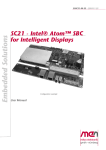
SC21 – Intel® Atom™ SBC
for Intelligent Displays
Configuration example
User Manual
®
SC21 – Intel® Atom™ SBC for Intelligent Displays
SC21 – Intel® Atom™ SBC for Intelligent Displays
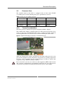
The SC21 is a rugged, fanless and maintenance-free single-board computer for
intelligent display devices, e.g., for infotainment purposes in trains, public buses or
airplanes. Its small size makes it suitable for display devices with TFT LCD panels
as small as 10.4".
The SC21 is controlled by the Intel® Atom™ XL Z520PT running at 1.33 GHz and
comes with 1 GB of DDR2 SDRAM and a MicroSD card slot. The standard
interfaces comprise 2 Fast Ethernet (via RJ45 connectors) and 2 USB ports as well
as four binary inputs (via the 10-pin power supply connector). The two Ethernet
interfaces have switch functionality to provide Ethernet connection to subsequent
intelligent displays. A temperature sensor is provided to monitor and control the
display. With the exception of the LVDS signals and the display backlight
brightness control, all I/O signals are concentrated on a customizable connector
PCB, including a USB-driven connector for a touch interface.
The SC21 is equipped with an internal 9 to 36V (12VDC nom. or 24VDC nom.)
wide-range power supply and able to operate in a -40 to +70°C environment (+85°C
for 10 minutes) with sufficient cooling. It complies with the class Tx railway
standard, an optionally available external PSU suited for railway applications can
also provide EN 50155 conformity. All electronic components are soldered to
withstand shock and vibration and prepared for conformal coating.
Options include other types of the Intel® Atom™ XL processor, a brightness sensor
to control the display, a serial interface that can be added via an SA-Adapter™, HD
audio via a D-Sub connector and an additional LVDS connection for a secondary
display, with the two displays then showing individual or identical content as
required by the application. A PCI Express® Mini Card slot (with a SIM card slot)
in combination with an external antenna can be used to incorporate wireless
functions like WIFI, WIMAX, GSM/GPRS, UMTS etc.
MEN Mikro Elektronik GmbH
20SC21-00 E7 – 2012-10-04
2
Technical Data
Technical Data
CPU
• Intel® Atom™ Z520PT
- 1.33 GHz processor core frequency
- 533 MHz system bus frequency
• Chipset
- Intel® system controller hub US15W
Memory
• 1GB DDR2 SDRAM system memory
- Soldered
- 533 MHz memory bus frequency
• MicroSD card slot
• SATA interface for HDD/SSD
- Transfer rates up to 100 MB/s
Graphics
• 1 LVDS 25-pin connector
- For direct connection of an LVDS display with a resolution of up to
1366x768 (secondary interface with up to 1900x1200)
• 1 LVDS backlight 10-pin connector
- Brightness control via software
PCI Express® Mini Card slot
•
•
•
•
For functions like WIFI, WIMAX, GSM/GPRS, UMTS
SIM card slot
PCI Express® and USB interface
Accessible via, e.g., a reverse SMA connector
I/O
• USB
- Two USB 2.0 host ports
- Accessible via Series A connectors
- UHCI implementation
- Data rates up to 480 Mbit/s
• Ethernet
- Two 10/100Base-T Ethernet channels
- Accessible via RJ45 connectors
- Switch functionality
• Touch interface connector
- USB-driven 4-pin connector
- Touch technology depending on touch sensor, touch controller and software
• 4 binary inputs via 10-pin power connector
- Universal inputs, e.g., for geographical addressing
MEN Mikro Elektronik GmbH
20SC21-00 E7 – 2012-10-04
3
Technical Data
Intelligent Power Supply with Controller
•
•
•
•
•
•
•
•
Voltage supervision
Temperature supervision via LM50 sensor
Backlight control (turns off display at configurable temperatures)
Buffer functionality for RTC and BIOS CMOS
Reset of CPU board possible
Wake on time
Watchdog
Accessible via SMBus
Electrical Specifications
• Supply voltage:
- 12 VDC nom. or 24 VDC nom. (9 to 36 V)
• Power consumption:
- Ca. 8 W (without display)
Mechanical Specifications
• Dimensions: 220 mm x 150 mm x 35 mm
• Weight: approx. 240 g (320 g with heat sink)
Environmental Specifications
• Temperature range (operation):
- -40°C to 70°C, with up to 85°C for 10 minutes according to class Tx
(EN 50155) depending on cooling concept (sufficient cooling required)
- Prepared for conductive cooling (via connection from mounting frame to
metal display housing)
- Fanless operation
• Temperature range (storage): -40..+85°C
• Relative humidity (operation): max. 95% non-condensing
• Relative humidity (storage): max. 95% non-condensing
• Altitude: -300 m to + 3,000 m
• Shock: according to EN 50155 (10.2.11)
• Vibration: according to EN 50155 (10.2.11)
MTBF
• 213,000 h @ 40°C according to IEC/TR 62380 (RDF 2000)
EMC
• Conforming to EN 50155, EN 50121-3-2/EN 61000-4-5
• Conforming to e1 requirements of the German Federal Motor Transport
Authority
Software Support
• Windows® XP Embedded
• Linux
• For more information on supported operating system versions and drivers see
online data sheet.
MEN Mikro Elektronik GmbH
20SC21-00 E7 – 2012-10-04
4
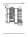
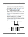
Block Diagram
Block Diagram
Options
R
Rear I/O connector
B
On‐board connector
Temperature
Sensor
SIM Card
R
Power Supply
MiniPCI Express® Card
R
USB 2.0
USB 2.0
R
USB 2.0
USB 2.0
USB 2.0
MicroSD card
R
SA‐
Adapter
Touch
USB‐to‐Serial Bridge
USB 2.0
10/100Base‐T Ethernet
R
R
COM
Connector
PCB
USB 2.0
Intel® Atom™ XL
Processor and
Intel® System Controller Hub
R
SATA HDD/SSD
1 GB
DDR2 SDRAM
I2C
HD Audio
SDVO
MEN Mikro Elektronik GmbH
20SC21-00 E7 – 2012-10-04
USB 2.0
Flash SSD
10/100Base‐T Ethernet
Dual Ethernet Controller with Switch Functionality
Bright‐
ness Sensor
MicroSD card
SDVO‐to‐
LVDS
LVDS 1
B
Backlight Control 1
B
LVDS 2
B
Backlight Control 2
B
5
Configuration Options
Configuration Options
CPU
•
•
•
•
Intel® Atom™ Z530P, 1.6 GHz, 533 MHz FSB
Intel® Atom™ Z510P, 1.1 GHz, 400 MHz FSB
Intel® Atom™ Z520PT, 1.33 GHz, 533 MHz FSB
Intel® Atom™ Z510PT, 1.1 GHz, 400 MHz FSB
Graphics
• 8-bit LVDS for secondary display via SDVO-to-LVDS converter
- Resolution: Up to 1920x1200
- Backlight control via brightness sensor
Memory
• Second MicroSD card slot
• USB Flash SSD
- Up to 8 GB
PCI Express® Mini Card slot
• Slot compatible with half-size modules
I/O
• Ethernet
- 2 Fast Ethernet on M12 connectors
• HD audio
- HD audio codec
- Audio stereo in
- Audio stereo out
- SPDIF out
- All available via 9-pin D-Sub connector
• Serial interface
- 1 serial interface realized via SA-Adapter™, e.g., RS232 or RS422, isolated
or not, IBIS
• Custom connector available instead of standard I/O interface board
Electrical Specifications
• External PSU suited for railway applications
As the product concept is very flexible, there are many other configuration
possibilities. Please contact our sales team if you do not find your required
function in the options.
For available standard configurations see online data sheet.
MEN Mikro Elektronik GmbH
20SC21-00 E7 – 2012-10-04
6
Product Safety
Product Safety
!
Electrostatic Discharge (ESD)
Computer boards and components contain electrostatic sensitive devices.
Electrostatic discharge (ESD) can damage components. To protect the board and
other components against damage from static electricity, you should follow some
precautions whenever you work on your computer.
• Power down and unplug your computer system when working on the inside.
• Hold components by the edges and try not to touch the IC chips, leads, or circuitry.
• Use a grounded wrist strap before handling computer components.
• Place components on a grounded antistatic pad or on the bag that came with the
component whenever the components are separated from the system.
• Store the board only in its original ESD-protected packaging. Retain the original
packaging in case you need to return the board to MEN for repair.
MEN Mikro Elektronik GmbH
20SC21-00 E7 – 2012-10-04
7
About this Document
About this Document
This user manual describes the hardware functions of the board, connection of
peripheral devices and integration into a system. It also provides additional
information for special applications and configurations of the board.
The manual does not include detailed information on individual components (data
sheets etc.). A list of literature is given in the appendix.
History
Issue
Comments
Date
E1
First issue
2010-11-10
E2
Fixed hyperlink in board supervision chapter
Cosmetics
2010-11-25
E3
Added warning regarding connection of both Ethernet ports to the same switch in powerless state
2011-06-24
Reworked/corrected chapter on Ethernet and general status LEDs
Added Firmware Functions chapter
Reworked EEPROM sub-chapter
Updated SMBus devices table
Clarified position of pins of the power supply connector
E4
New touch interface connector position/pinning
2011-08-09
Minor changes
E5
Added information regarding connection of isolated
ground (power connector) to system ground
Added exact weight with and without heat sink
2011-11-21
E6
Added operating temperature restriction
2012-02-15
E7
Updated Chapter 2.10 LVDS Interfaces on page 25,
Chapter 2.4 Real-Time Clock on page 19 and
Chapter 3 Firmware Functions on page 35
2012-10-04
MEN Mikro Elektronik GmbH
20SC21-00 E7 – 2012-10-04
8
About this Document
Conventions
This sign marks important notes or warnings concerning the use of voltages which
can lead to serious damage to your health and also cause damage or destruction of
the component.
!
italics
bold
monospace
This sign marks important notes or warnings concerning proper functionality of the
product described in this document. You should read them in any case.
Folder, file and function names are printed in italics.
Bold type is used for emphasis.
A monospaced font type is used for hexadecimal numbers, listings, C function
descriptions or wherever appropriate. Hexadecimal numbers are preceded by "0x".
comment
Comments embedded into coding examples are shown in green color.
hyperlink
Hyperlinks are printed in blue color.
The globe will show you where hyperlinks lead directly to the Internet, so you can
look for the latest information online.
IRQ#
/IRQ
Signal names followed by "#" or preceded by a slash ("/") indicate that this signal is
either active low or that it becomes active at a falling edge.
in/out
Signal directions in signal mnemonics tables generally refer to the corresponding
board or component, "in" meaning "to the board or component", "out" meaning
"coming from it".
Vertical lines on the outer margin signal technical changes to the previous issue of
the document.
MEN Mikro Elektronik GmbH
20SC21-00 E7 – 2012-10-04
9
About this Document
Legal Information
Changes
MEN Mikro Elektronik GmbH ("MEN") reserves the right to make changes without further notice to any products
herein.
Warranty, Guarantee, Liability
MEN makes no warranty, representation or guarantee of any kind regarding the suitability of its products for any
particular purpose, nor does MEN assume any liability arising out of the application or use of any product or
circuit, and specifically disclaims any and all liability, including, without limitation, consequential or incidental
damages. TO THE EXTENT APPLICABLE, SPECIFICALLY EXCLUDED ARE ANY IMPLIED
WARRANTIES ARISING BY OPERATION OF LAW, CUSTOM OR USAGE, INCLUDING WITHOUT
LIMITATION, THE IMPLIED WARRANTIES OF MERCHANTABILITY AND FITNESS FOR A
PARTICULAR PURPOSE OR USE. In no event shall MEN be liable for more than the contract price for the
products in question. If buyer does not notify MEN in writing within the foregoing warranty period, MEN shall
have no liability or obligation to buyer hereunder.
The publication is provided on the terms and understanding that:
1. MEN is not responsible for the results of any actions taken on the basis of information in the publication, nor
for any error in or omission from the publication; and
2. MEN is not engaged in rendering technical or other advice or services.
MEN expressly disclaims all and any liability and responsibility to any person, whether a reader of the publication
or not, in respect of anything, and of the consequences of anything, done or omitted to be done by any such person
in reliance, whether wholly or partially, on the whole or any part of the contents of the publication.
Conditions for Use, Field of Application
The correct function of MEN products in mission-critical and life-critical applications is limited to the
environmental specification given for each product in the technical user manual. The correct function of MEN
products under extended environmental conditions is limited to the individual requirement specification and
subsequent validation documents for each product for the applicable use case and has to be agreed upon in writing
by MEN and the customer. Should the customer purchase or use MEN products for any unintended or
unauthorized application, the customer shall indemnify and hold MEN and its officers, employees, subsidiaries,
affiliates, and distributors harmless against all claims, costs, damages, and expenses, and reasonable attorney fees
arising out of, directly or indirectly, any claim or personal injury or death associated with such unintended or
unauthorized use, even if such claim alleges that MEN was negligent regarding the design or manufacture of the
part. In no case is MEN liable for the correct function of the technical installation where MEN products are a part
of.
Trademarks
All products or services mentioned in this publication are identified by the trademarks, service marks, or product
names as designated by the companies which market those products. The trademarks and registered trademarks
are held by the companies producing them. Inquiries concerning such trademarks should be made directly to those
companies.
Conformity
MEN products are no ready-made products for end users. They are tested according to the standards given in the
Technical Data and thus enable you to achieve certification of the product according to the standards applicable in
your field of application.
MEN Mikro Elektronik GmbH
20SC21-00 E7 – 2012-10-04
10
About this Document
RoHS
Since July 1, 2006 all MEN standard products comply with RoHS legislation.
Since January 2005 the SMD and manual soldering processes at MEN have already been completely lead-free.
Between June 2004 and June 30, 2006 MEN’s selected component suppliers have changed delivery to RoHScompliant parts. During this period any change and status was traceable through the MEN ERP system and the
boards gradually became RoHS-compliant.
WEEE Application
The WEEE directive does not apply to fixed industrial plants and tools. The compliance is the responsibility of the
company which puts the product on the market, as defined in the directive; components and sub-assemblies are
not subject to product compliance.
In other words: Since MEN does not deliver ready-made products to end users, the WEEE directive is not
applicable for MEN. Users are nevertheless recommended to properly recycle all electronic boards which have
passed their life cycle.
Nevertheless, MEN is registered as a manufacturer in Germany. The registration number can be provided on
request.
Copyright © 2012 MEN Mikro Elektronik GmbH. All rights reserved.
Germany
MEN Mikro Elektronik GmbH
Neuwieder Straße 3-7
90411 Nuremberg
Phone +49-911-99 33 5-0
Fax +49-911-99 33 5-901
E-mail [email protected]
www.men.de
MEN Mikro Elektronik GmbH
20SC21-00 E7 – 2012-10-04
France
MEN Mikro Elektronik SA
18, rue René Cassin
ZA de la Châtelaine
74240 Gaillard
Phone +33 (0) 450-955-312
Fax +33 (0) 450-955-211
E-mail [email protected]
www.men-france.fr
USA
MEN Micro, Inc.
24 North Main Street
Ambler, PA 19002
Phone (215) 542-9575
Fax (215) 542-9577
E-mail [email protected]
www.menmicro.com
11
Contents
Contents
1 Getting Started . . . . . . . . . . . . . . . . . . . . . . . . . . . . . . . . . . . . . . . . . . . . . . . .
1.1 Map of the Board. . . . . . . . . . . . . . . . . . . . . . . . . . . . . . . . . . . . . . . . .
1.2 First Operation. . . . . . . . . . . . . . . . . . . . . . . . . . . . . . . . . . . . . . . . . . .
1.3 Installing Operating System Software. . . . . . . . . . . . . . . . . . . . . . . . .
1.4 Installing Driver Software . . . . . . . . . . . . . . . . . . . . . . . . . . . . . . . . . .
16
16
17
17
17
2 Functional Description . . . . . . . . . . . . . . . . . . . . . . . . . . . . . . . . . . . . . . . . . .
2.1 Power Supply. . . . . . . . . . . . . . . . . . . . . . . . . . . . . . . . . . . . . . . . . . . .
2.1.1
Power Input Ground Connection . . . . . . . . . . . . . . . . . . . . .
2.1.2
Binary inputs . . . . . . . . . . . . . . . . . . . . . . . . . . . . . . . . . . . . .
2.2 Board Supervision . . . . . . . . . . . . . . . . . . . . . . . . . . . . . . . . . . . . . . . .
2.3 Reset . . . . . . . . . . . . . . . . . . . . . . . . . . . . . . . . . . . . . . . . . . . . . . . . . .
2.4 Real-Time Clock . . . . . . . . . . . . . . . . . . . . . . . . . . . . . . . . . . . . . . . . .
2.5 Processor Core. . . . . . . . . . . . . . . . . . . . . . . . . . . . . . . . . . . . . . . . . . .
2.5.1
Thermal Considerations . . . . . . . . . . . . . . . . . . . . . . . . . . . .
2.6 Memory . . . . . . . . . . . . . . . . . . . . . . . . . . . . . . . . . . . . . . . . . . . . . . . .
2.6.1
DRAM System Memory . . . . . . . . . . . . . . . . . . . . . . . . . . . .
2.6.2
Boot Flash . . . . . . . . . . . . . . . . . . . . . . . . . . . . . . . . . . . . . . .
2.6.3
EEPROM. . . . . . . . . . . . . . . . . . . . . . . . . . . . . . . . . . . . . . . .
2.7 Mass Storage . . . . . . . . . . . . . . . . . . . . . . . . . . . . . . . . . . . . . . . . . . . .
2.7.1
microSD Card Interface . . . . . . . . . . . . . . . . . . . . . . . . . . . .
2.7.2
Serial ATA (SATA) . . . . . . . . . . . . . . . . . . . . . . . . . . . . . . . .
2.7.3
USB Flash SSD (optional) . . . . . . . . . . . . . . . . . . . . . . . . . .
2.8 PCI Express . . . . . . . . . . . . . . . . . . . . . . . . . . . . . . . . . . . . . . . . . . . . .
2.8.1
PCI Express Mini Card Interface . . . . . . . . . . . . . . . . . . . . .
2.9 Graphics. . . . . . . . . . . . . . . . . . . . . . . . . . . . . . . . . . . . . . . . . . . . . . . .
2.10 LVDS Interfaces . . . . . . . . . . . . . . . . . . . . . . . . . . . . . . . . . . . . . . . . .
2.10.1 LVDS Backlight . . . . . . . . . . . . . . . . . . . . . . . . . . . . . . . . . .
2.11 Brightness Sensor (optional) . . . . . . . . . . . . . . . . . . . . . . . . . . . . . . . .
2.12 USB Interface . . . . . . . . . . . . . . . . . . . . . . . . . . . . . . . . . . . . . . . . . . .
2.13 Ethernet Interface . . . . . . . . . . . . . . . . . . . . . . . . . . . . . . . . . . . . . . . .
2.14 Ethernet and General Status LEDs . . . . . . . . . . . . . . . . . . . . . . . . . . .
2.15 I2C Interface . . . . . . . . . . . . . . . . . . . . . . . . . . . . . . . . . . . . . . . . . . . .
2.16 Touch Interface . . . . . . . . . . . . . . . . . . . . . . . . . . . . . . . . . . . . . . . . . .
2.16.1 Serial Interface via SA-Adapter (optional) . . . . . . . . . . . . . .
2.17 Audio (optional) . . . . . . . . . . . . . . . . . . . . . . . . . . . . . . . . . . . . . . . . .
18
18
18
18
19
19
19
20
20
21
21
21
21
21
21
22
23
23
23
25
25
28
28
29
30
31
33
33
33
34
3 Firmware Functions . . . . . . . . . . . . . . . . . . . . . . . . . . . . . . . . . . . . . . . . . . . .
3.1 Board Management Controller (BMC) . . . . . . . . . . . . . . . . . . . . . . . .
3.1.1
Available Functions. . . . . . . . . . . . . . . . . . . . . . . . . . . . . . . .
3.2 Power and Display Management Controller (PMC) . . . . . . . . . . . . . .
3.2.1
Available Functions. . . . . . . . . . . . . . . . . . . . . . . . . . . . . . . .
3.3 SMBus Functionality. . . . . . . . . . . . . . . . . . . . . . . . . . . . . . . . . . . . . .
3.3.1
SMBus Interface . . . . . . . . . . . . . . . . . . . . . . . . . . . . . . . . . .
35
35
36
36
37
38
38
MEN Mikro Elektronik GmbH
20SC21-00 E7 – 2012-10-04
12
Contents
3.3.2
3.3.3
3.3.4
3.3.5
3.3.6
3.3.7
3.3.8
3.3.9
3.3.10
3.3.11
Wake On Time. . . . . . . . . . . . . . . . . . . . . . . . . . . . . . . . . . . .
Status of Binary Inputs . . . . . . . . . . . . . . . . . . . . . . . . . . . . .
Key Input. . . . . . . . . . . . . . . . . . . . . . . . . . . . . . . . . . . . . . . .
SMBus On Acknowledge . . . . . . . . . . . . . . . . . . . . . . . . . . .
Shutdown. . . . . . . . . . . . . . . . . . . . . . . . . . . . . . . . . . . . . . . .
Shutdown Delay . . . . . . . . . . . . . . . . . . . . . . . . . . . . . . . . . .
Voltage Supervision . . . . . . . . . . . . . . . . . . . . . . . . . . . . . . .
Temperature Supervision . . . . . . . . . . . . . . . . . . . . . . . . . . .
Display Backlight Power and Brightness Control . . . . . . . .
Optional Autonomous Brightness Control with
Photo Diode. . . . . . . . . . . . . . . . . . . . . . . . . . . . . . . . . . . . . .
Miscellaneous Commands . . . . . . . . . . . . . . . . . . . . . . . . . .
38
39
39
39
40
41
43
43
44
4 BIOS . . . . . . . . . . . . . . . . . . . . . . . . . . . . . . . . . . . . . . . . . . . . . . . . . . . . . . . . .
4.1 Main Menu . . . . . . . . . . . . . . . . . . . . . . . . . . . . . . . . . . . . . . . . . . . . .
4.2 Standard CMOS Features . . . . . . . . . . . . . . . . . . . . . . . . . . . . . . . . . .
4.3 Advanced BIOS Features . . . . . . . . . . . . . . . . . . . . . . . . . . . . . . . . . .
4.4 Advanced Chipset Features . . . . . . . . . . . . . . . . . . . . . . . . . . . . . . . . .
4.5 Integrated Peripherals . . . . . . . . . . . . . . . . . . . . . . . . . . . . . . . . . . . . .
4.6 Power Management Setup . . . . . . . . . . . . . . . . . . . . . . . . . . . . . . . . . .
4.7 PNP/PCI Configurations . . . . . . . . . . . . . . . . . . . . . . . . . . . . . . . . . . .
4.8 PC Health Status . . . . . . . . . . . . . . . . . . . . . . . . . . . . . . . . . . . . . . . . .
4.9 Frequency/Voltage Control . . . . . . . . . . . . . . . . . . . . . . . . . . . . . . . . .
4.10 Load Fail-Safe Defaults. . . . . . . . . . . . . . . . . . . . . . . . . . . . . . . . . . . .
4.11 Load Optimized Defaults. . . . . . . . . . . . . . . . . . . . . . . . . . . . . . . . . . .
4.12 Set Password . . . . . . . . . . . . . . . . . . . . . . . . . . . . . . . . . . . . . . . . . . . .
4.13 Save & Exit Setup . . . . . . . . . . . . . . . . . . . . . . . . . . . . . . . . . . . . . . . .
4.14 Exit without Saving . . . . . . . . . . . . . . . . . . . . . . . . . . . . . . . . . . . . . . .
46
46
47
49
53
55
58
60
62
62
63
63
63
63
63
5 Organization of the Board . . . . . . . . . . . . . . . . . . . . . . . . . . . . . . . . . . . . . . .
5.0.1
Processor View of the Memory Map. . . . . . . . . . . . . . . . . . .
5.0.2
I/O Memory Map . . . . . . . . . . . . . . . . . . . . . . . . . . . . . . . . .
5.1 PCI Devices . . . . . . . . . . . . . . . . . . . . . . . . . . . . . . . . . . . . . . . . . . . . .
5.2 SMBus Devices . . . . . . . . . . . . . . . . . . . . . . . . . . . . . . . . . . . . . . . . . .
5.3 Interrupt Mapping . . . . . . . . . . . . . . . . . . . . . . . . . . . . . . . . . . . . . . . .
64
64
65
66
67
67
6 Appendix . . . . . . . . . . . . . . . . . . . . . . . . . . . . . . . . . . . . . . . . . . . . . . . . . . . . .
6.1 Literature and Web Resources . . . . . . . . . . . . . . . . . . . . . . . . . . . . . . .
6.1.1
CPU . . . . . . . . . . . . . . . . . . . . . . . . . . . . . . . . . . . . . . . . . . . .
6.1.2
SATA . . . . . . . . . . . . . . . . . . . . . . . . . . . . . . . . . . . . . . . . . . .
6.1.3
USB . . . . . . . . . . . . . . . . . . . . . . . . . . . . . . . . . . . . . . . . . . . .
6.1.4
Ethernet . . . . . . . . . . . . . . . . . . . . . . . . . . . . . . . . . . . . . . . . .
6.1.5
HD Audio . . . . . . . . . . . . . . . . . . . . . . . . . . . . . . . . . . . . . . .
6.1.6
PCI Express. . . . . . . . . . . . . . . . . . . . . . . . . . . . . . . . . . . . . .
6.1.7
PCI Express Mini Card . . . . . . . . . . . . . . . . . . . . . . . . . . . . .
6.2 Finding out the Product’s Article Number, Revision and
Serial Number . . . . . . . . . . . . . . . . . . . . . . . . . . . . . . . . . . . . . . . . . . .
68
68
68
68
68
68
68
69
69
3.3.12
MEN Mikro Elektronik GmbH
20SC21-00 E7 – 2012-10-04
45
45
69
13
Figures
Figure 1.
Figure 2.
Figure 3.
Figure 4.
Figure 5.
Figure 6.
Figure 7.
Map of the board. . . . . . . . . . . . . . . . . . . . . . . . . . . . . . . . . . . . . . . . . .
Coding connector . . . . . . . . . . . . . . . . . . . . . . . . . . . . . . . . . . . . . . . . .
Optional mounting screw hole on standard heat sink. . . . . . . . . . . . . .
Position of Ethernet and general status LEDs on connector board . . .
Position of I2C and touch interface connectors on connector PCB . . .
Microcontroller block diagram. . . . . . . . . . . . . . . . . . . . . . . . . . . . . . .
Labels giving the product’s article number, revision and
serial number . . . . . . . . . . . . . . . . . . . . . . . . . . . . . . . . . . . . . . . . . . . .
16
19
20
31
33
35
Power supply VCC / coding connector pin assignment . . . . . . . . . . . .
Processor core options on SC21 . . . . . . . . . . . . . . . . . . . . . . . . . . . . . .
Pin assignment of SATA connector . . . . . . . . . . . . . . . . . . . . . . . . . . .
Signal mnemonics of SATA connector . . . . . . . . . . . . . . . . . . . . . . . .
Pin assignment of 52-pin PCI Express Mini Card connector. . . . . . . .
Signal mnemonics of 52-pin PCI Express Mini Card connector . . . . .
Primary LVDS pin assignment. . . . . . . . . . . . . . . . . . . . . . . . . . . . . . .
Secondary LVDS pin assignment. . . . . . . . . . . . . . . . . . . . . . . . . . . . .
Optional secondary LVDS pin assignment . . . . . . . . . . . . . . . . . . . . .
Primary LVDS backlight connector pin assignment . . . . . . . . . . . . . .
Secondary LVDS backlight connector pin assignment . . . . . . . . . . . .
Pin assignment of USB front-panel connectors . . . . . . . . . . . . . . . . . .
Pin assignment of the 8-pin RJ45 Ethernet
10/100Base-T connectors . . . . . . . . . . . . . . . . . . . . . . . . . . . . . . . . . . .
Ethernet and general status LEDs
(from top to bottom as depicted above) . . . . . . . . . . . . . . . . . . . . . . . .
Error codes signaled by BMC via LED flashes
(red BMC 2 status LED). . . . . . . . . . . . . . . . . . . . . . . . . . . . . . . . . . . .
I2C interface connector pin assignment . . . . . . . . . . . . . . . . . . . . . . . .
Touch interface connector pin assignment . . . . . . . . . . . . . . . . . . . . . .
Pin assignment of the HD audio interface . . . . . . . . . . . . . . . . . . . . . .
Signal mnemonics of the HD audio interface. . . . . . . . . . . . . . . . . . . .
SMBus commands for the watchdog function . . . . . . . . . . . . . . . . . . .
SMBus command XC02C_WDOG_TOUT . . . . . . . . . . . . . . . . . . . . .
SMBus commands for wake on time function . . . . . . . . . . . . . . . . . . .
SMBus commands XC02C_WOT_L / XC02C_WOT_H . . . . . . . . . .
SMBus commands for binary inputs status . . . . . . . . . . . . . . . . . . . . .
SMBus commands for On acknowledge function . . . . . . . . . . . . . . . .
SMBus On acknowledge timer modes . . . . . . . . . . . . . . . . . . . . . . . . .
SMBus command for shutdown by software function . . . . . . . . . . . . .
18
20
22
22
23
24
25
26
27
28
28
29
69
Tables
Table 1.
Table 2.
Table 3.
Table 4.
Table 5.
Table 6.
Table 7.
Table 8.
Table 9.
Table 10.
Table 11.
Table 12.
Table 13.
Table 14.
Table 15.
Table 16.
Table 17.
Table 18.
Table 19.
Table 20.
Table 21.
Table 22.
Table 23.
Table 24.
Table 25.
Table 26.
Table 27.
MEN Mikro Elektronik GmbH
20SC21-00 E7 – 2012-10-04
30
31
32
33
33
34
34
36
37
38
38
39
40
40
40
14
Table 28.
Table 29.
Table 30.
Table 31.
Table 32.
Table 33.
Table 34.
Table 35.
Table 36.
Table 37.
Table 38.
Table 39.
Table 40.
Table 41.
Table 42.
Table 43.
MEN Mikro Elektronik GmbH
20SC21-00 E7 – 2012-10-04
SMBus commands for shutdown delay . . . . . . . . . . . . . . . . . . . . . . . .
SMBus command XC02C_STATUS . . . . . . . . . . . . . . . . . . . . . . . . . .
SMBus command XC02C_DOWN_DELAY . . . . . . . . . . . . . . . . . . .
SMBus command for Off delay function . . . . . . . . . . . . . . . . . . . . . . .
SMBus command XC02C_OFF_DELAY . . . . . . . . . . . . . . . . . . . . . .
SMBus command for Off acknowledge function. . . . . . . . . . . . . . . . .
SMBus command for voltage supervision function . . . . . . . . . . . . . . .
SMBus commands for temperature supervision. . . . . . . . . . . . . . . . . .
Temperature representation . . . . . . . . . . . . . . . . . . . . . . . . . . . . . . . . .
SMBus commands for display control . . . . . . . . . . . . . . . . . . . . . . . . .
SMBus commands for PSU ID and firmware revision number . . . . . .
Memory map – processor view . . . . . . . . . . . . . . . . . . . . . . . . . . . . . .
Memory map - I/O . . . . . . . . . . . . . . . . . . . . . . . . . . . . . . . . . . . . . . . .
PCI Devices . . . . . . . . . . . . . . . . . . . . . . . . . . . . . . . . . . . . . . . . . . . . .
SMBus devices . . . . . . . . . . . . . . . . . . . . . . . . . . . . . . . . . . . . . . . . . . .
Interrupts. . . . . . . . . . . . . . . . . . . . . . . . . . . . . . . . . . . . . . . . . . . . . . . .
41
41
41
42
42
42
43
44
44
45
45
64
65
66
67
67
15
Getting Started
1
Getting Started
This chapter gives an overview of the board and some hints for first installation in a
system.
1.1
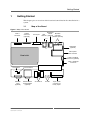
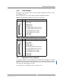
Map of the Board
Figure 1. Map of the board
LVDS 2
connector
(optional)
LVDS 1
connector
SATA port
Brightness
sensor
MicroSD
SIM
(optional)
card slots
card slot
(left slot optional)
Ejector
USB Flash
(optional)
PCI Express
Mini Card slot
Heat sink
LVDS 2 backlight
connector (optional)
LVDS 1 backlight
connector
I2C interface
Touch interface
1
1
HD audio
in/out
(optional)
Serial interface
via SA-Adapter
(optional)
MEN Mikro Elektronik GmbH
20SC21-00 E7 – 2012-10-04
2x Ethernet
2x USB
10-pin power
connector w/
binary inputs
16
Getting Started
1.2
First Operation
You can use the following check list when installing the board for the first time and
with minimum configuration.
Connect a USB keyboard and mouse to the USB connectors of the SC21.
Connect a flat-panel display capable of displaying the resolution of 1024x786
to the LVDS connector of the SC21.
Power-up the system.
You can start up the BIOS setup menu by hitting the <DEL> key (see Chapter 4
BIOS on page 46).
Now you can make configurations in BIOS (see Chapter 4 BIOS on page 46).
Observe the installation instructions for the respective software.
1.3
Installing Operating System Software
The board supports Windows XP Embedded and Linux (on request).
!
By default, no operating system is installed on the board. Please refer to the
operating system installation documentation on how to install the software!
You can find any software available on MEN’s website.
1.4
Installing Driver Software
For a detailed description on how to install driver software please refer to the
respective documentation.
You can find any driver software available for download on MEN’s website.
MEN Mikro Elektronik GmbH
20SC21-00 E7 – 2012-10-04
17
Functional Description
2
Functional Description
The following describes the individual functions of the board and their
configuration on the board. There is no detailed description of the individual
controller chips and the CPU. They can be obtained from the data sheets or data
books of the semiconductor manufacturer concerned (Chapter 6.1 Literature and
Web Resources on page 68).
Please note that the board BSPs for the different operating systems may not support
all the functions of the SC21. For more information on hardware support please see
the respective BSP data sheet on MEN’s website.
2.1
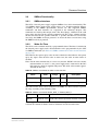
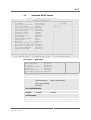
Power Supply
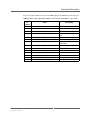
The SC21 is supplied with a nominal voltage of 12 V or 24 V (9..36 VDC). All
other required voltages are generated onboard. The SC21 provides one 10-pin
spring-type terminal that is also used for the unit’s binary inputs. Pin 1 is located on
the USB connector side.
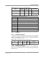
Table 1. Power supply VCC / coding connector pin assignment
Pin
1
10
2.1.1
!
Name
Description
1
9-36VDC
Power input
2
IGND
GND power input
3
BININ0
Binary0 coding input
4
V_IN(BININ)
VSupply and BININ0 supply
5
BININ1
Binary1 coding input
6
V_IN(BININ)
VSupply and BININ1 supply
7
BININ2
Binary2 coding input
8
V_IN(BININ)
VSupply and BININ2 supply
9
BININ3
Binary3 coding input
10
V_IN(BININ)
VSupply and BININ3 supply
Power Input Ground Connection
Please note that the IGND described above is separated from the system GND by a
switch. The switch connects IGND with system GND when the board is in powered
state (with the key input signal active!). There is no connection between the two
when the board is in non-powered state.
2.1.2
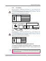
Binary inputs
The SC21 provides 4 binary inputs. The maximum input voltage is 36 VDC. The
threshold voltage is 6 V. The binary inputs are protected via suppressor diodes. To
provide a simple circuit, the inputs are realized without galvanic isolation. The
binary inputs are connected to the BMC. ESD and burst protection according to EN
50155 is guaranteed. To provide a coding function with the binary inputs, the supply
voltage is connectable to the binary inputs with a cable bridge on the connector.
MEN Mikro Elektronik GmbH
20SC21-00 E7 – 2012-10-04
18
Functional Description
2.2
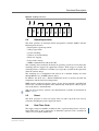
VSupply
BIN_IN4
VSupply
BIN_IN3
VSupply
BIN_IN2
VSupply
BIN_IN1
GND
VIN
Figure 2. Coding connector
Board Supervision
The SC21 provides an intelligent board management controller (BMC) with the
following main features:
•
•
•
•
•
•
•
Board power sequencing control
Voltage supervision
System watchdog
Software reset functionality
Error state logging
Power mode settings
SMBus communication with main CPU
The watchdog device monitors the board on operating system level. If enabled, the
watchdog must be triggered by application software. If the trigger is overdue, the
watchdog initiates a board reset and this way can put the system back into operation
when the software hangs.
The watchdog uses a configurable time interval or is disabled. Settings are made
through BIOS or via an MEN software driver.
In addition, the SC21 uses a National LM95245 device to measure the CPU die
temperature and the local board temperature.
MEN provides dedicated software drivers for the board controller and LM95245
device. For a detailed description of the functionality of the driver software please
refer to the drivers’ documentation.
You can find any driver software and documentation available for download on
MEN’s website.
2.3
Reset
The SC21 generates its own reset signal. You can wake it up from reset state by
externally switching the power supply off and on.
2.4
Real-Time Clock
The supply voltage for the RTC is buffered with a capacitor that provides at least 12
hours buffer time at 40°C. Optionally an additional capacitor can be assembled to
achieve at least 24 hours buffer time.
MEN Mikro Elektronik GmbH
20SC21-00 E7 – 2012-10-04
19
Functional Description
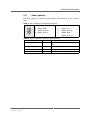
2.5
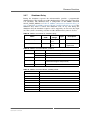
Processor Core
The standard model of the SC21 is equipped with an Intel Atom Z520PT
(1.33 GHz) processor. The following table gives a performance overview:
Table 2. Processor core options on SC21
Processor Type
Core Frequency
L2 Cache
Front Side Bus
Atom Z510P
1.1 GHz
512 KB
400 MHz
Atom Z530P
1.6 GHz
512 KB
533 MHz
Atom Z510PT
1.1GHz
512 KB
400MHz
Atom Z520PT
1.33GHz
512 KB
533MHz
2.5.1
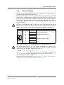
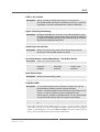
Thermal Considerations
The SC21 generates around 8 W of power dissipation (without a display).
The standard SC21 model is equipped with a heat sink. Note that only three of its
screws are necessary to hold the heat sink in place, a fourth screw hole (marked in
red in the photo below) can alternatively be used for mounting the SC21 board.
Figure 3. Optional mounting screw hole on standard heat sink
While the standard SC21 model is designed for convection cooling, the unit is also
prepared for conductive cooling. The SC21 is prepared for an operating temperature
of -40 to +85°C depending on the cooling concept. In order to achieve this
temperature range, sufficient cooling is required.
!
Please note that if you do not use the heat sink supplied by MEN and/or no heat
sink, warranty on functionality and reliability of the SC21 may cease. If you have
any questions or problems regarding thermal behavior, please contact MEN.
MEN Mikro Elektronik GmbH
20SC21-00 E7 – 2012-10-04
20
Functional Description
2.6
Memory
2.6.1
DRAM System Memory
The board provides 1 GB on-board, soldered DDR2 (double data rate) SDRAM.
The memory bus is 64 bits wide (one channel) and operates with up to 533 MHz.
2.6.2
Boot Flash
The SC21 has an 8-Mbit LPC Firmware Hub (FWH) implemented as on-board
Flash for BIOS data.
2.6.3
EEPROM
The board has two 2-kbit serial EEPROMs for factory data. One is used for the data
of the SC21, the other can be used for the data of the display computer.
The EEPROMs store the serial number, board revision, name, production date and
reparation date.
The MDIS tool smb2_eeprod2 can be used for comfortable access to the
configuration EEPROMs. See Table 42, SMBus devices on page 67.
2.7
Mass Storage
2.7.1
microSD Card Interface
The SC21 provides a USB-driven 4-bit slot for a standard microSD card. A second
microSD card slot is optional.
MEN Mikro Elektronik GmbH
20SC21-00 E7 – 2012-10-04
21
Functional Description
2.7.2
Serial ATA (SATA)
The SC21 provides one SATA interface that supports transfer rates up to 100 MB/s.
Table 3. Pin assignment of SATA connector
S1
GND
S2
SATA_TX+
S3
SATA_TX-
S4
GND
S5
SATA_RX-
S6
SATA_RX+
S7
GND
Key and spacing,
separate signal and
power segments
S1
P1
+3.3V (optional)
P2
+3.3V (optional)
P3
+3.3V (optional)
P4
GND
P5
GND
P6
GND
P7
+5V
P8
+5V
P9
+5V
P10
GND
P11
GND
P12
GND
P13
+12V
P14
+12V
P15
+12V
P1
Connector type:
• 7- & 15-pin SATA receptacle connector, 1.27mm pitch
Table 4. Signal mnemonics of SATA connector
Signal
Function
+12V
out
+12 V power supply (optional)
+3.3V
out
+3.3 V power supply
+5V
out
+5 V power supply
GND
-
Digital ground
SATA_RX+, SATA_RX-
in
Differential pair of SATA receive lines
SATA_TX+, SATA_TX-
out
Differential pair of SATA transmit lines
MEN Mikro Elektronik GmbH
20SC21-00 E7 – 2012-10-04
Direction
22
Functional Description
2.7.3
USB Flash SSD (optional)
Another optional mass storage solution for the SC21 is a USB-driven Flash SSD
(solid state drive).
2.8
PCI Express
The SC21 offers one PCI Express x1 link for the PCI Express Mini Card.
2.8.1
PCI Express Mini Card Interface
The SC21 supports the PCI Express Mini Card standard. As an option, it can also be
equipped with a PCI Express Mini Card slot compatible with half-size modules.
PCI Express Mini Cards are small form factor PCI Express cards. The main
differences between an ExpressCard and a PCI Express Mini Card is a smaller form
factor optimized for mobile computing platforms and a card-system Interconnection
optimized for communication applications. PCI Express Mini Cards also use
smaller connectors than standard ExpressCards.
The cards use either a single PCI Express lane (x1) or a USB connection; the SC21
supports both. It is equipped with one 52-pin standard PCI Express Mini Card
connector. The following standard signals are supported (signal directions according
to PCI Express Mini Card standard):
Table 5. Pin assignment of 52-pin PCI Express Mini Card connector
Pin
Pin
Signal
51
Reserved
52
+3.3Vaux
49
Reserved
50
GND
47
Reserved
48
+1.5V
45
Reserved
46
LED_WPAN#
43
GND
44
LED_WLAN#
41
+3.3Vaux
42
LED_WWAN#
39
+3.3Vaux
40
GND
37
GND
38
USB_D+
35
GND
36
USB_D-
33
PETp0
34
GND
31
PETn0
32
SMB_DATA
29
GND
30
SMB_CLK
27
GND
28
+1.5V
25
PERp0
26
GND
23
PERn0
24
+3.3Vaux
21
GND
22
PERST#
19
Reserved
20
Reserved
17
Reserved
18
GND
MEN Mikro Elektronik GmbH
20SC21-00 E7 – 2012-10-04
Signal
23
Functional Description
Pin
Signal
Pin
Signal
Mechanical Key
15
GND
16
UIM_VPP
13
REFCLK+
14
UIM_RST
11
REFCLK-
12
UIM_CLK
9
GND
10
UIM_DATA
7
CLKREQ#
8
UIM_PWR
5
Reserved
6
1.5V
3
Reserved
4
GND
1
WAKE#
2
+3.3Vaux
Table 6. Signal mnemonics of 52-pin PCI Express Mini Card connector
Signal
Power
SIM card
Direction
GND
-
Ground
+3.3Vaux
out
3.3V source
1.5V
out
1.5V source
UIM_PWR
out
SIM card power
UIM_DATA
in/out
SIM card data
UIM_CLK
out
SIM card clock
UIM_RST
out
SIM card reset
UIM_VPP
PCI
Express
Auxiliary
Signals
USB
Function
not connected
REFCLK-/REFCLK+
in
PCI Express differential reference
clock
PERn0/PERp0
out
PCI Express receive signals
PETn0/PETp0
in
PCI Express transmit signals
CLKREQ#
out
Clock request
PERST#
in
Reset for the Mini Card
WAKE#
out
Wake signal
SMB_CLK
in
System management bus clock
SMB_DATA
in/out
System management bus data
USB_D-
in/out
USB line
USB_D+
in/out
USB line
out
not connected
out
not connected
out
not connected
Communi- LED_WWAN#
cations LED_WLAN#
specific
LED_WPAN#
signals
Please refer to the PCI Express Mini Card Specification for further details. See
Chapter 6.1 Literature and Web Resources on page 68.
MEN Mikro Elektronik GmbH
20SC21-00 E7 – 2012-10-04
24
Functional Description
2.9
Graphics
2.10
LVDS Interfaces
The SC21 provides up to two LVDS interfaces with a 112 MHz maximum pixel
clock. The default one is a 4-bit LVDS interface and supports a resolution of up to
1366x768 pixels while the optional 8-bit LVDS interface goes up to 1920x1200.
The connector type is the 25-pin right angle DF14-25P-1.25H from Hirose.
Table 7. Primary LVDS pin assignment
Pin
1
25
MEN Mikro Elektronik GmbH
20SC21-00 E7 – 2012-10-04
Name
Description
Polarity
1
VDD
Power supply +3.3V nom.
2
VDD
Power supply +3.3V nom.
3
GND
Ground
4
GND
Ground
5
LVDS_DATA[3]+
LVDS differential data link 3
Positive
6
LVDS_DATA[3]-
LVDS differential data link 3
Negative
7
LVDS_CLK+
LVDS differential clock
Positive
8
LVDS_CLK-
LVDS differential clock
Negative
9
LVDS_DATA[2]+
LVDS differential data link 2
Positive
10
LVDS_DATA[2]-
LVDS differential data link 2
Negative
11
LVDS_DATA[1]+
LVDS differential data link 1
Positive
12
LVDS_DATA[1]-
LVDS differential data link 1
Negative
13
LVDS_DATA[0]+
LVDS differential data link 0
Positive
14
LVDS_DATA[0]-
LVDS differential data link 0
Negative
15
GND
Ground
16
GND
Ground
17
GND
Ground
18
GND
Ground
19
GND
Ground
20
GND
Ground
21
GND
Ground
22
GND
Ground
23
GND
Ground
24
GND
Ground
25
BL_ON
Backlight on +3.3V
MP1 NC
Not connected
MP2 NC
Not connected
25
Functional Description
Table 8. Secondary LVDS pin assignment
Pin
Description
Polarity
1
VDD
Power supply +3.3V nom.
2
VDD
Power supply +3.3V nom.
3
GND
Ground
4
GND
Ground
5
LVDS_OPT_DATA[3]+ LVDS differential data link 3
Positive
6
LVDS_OPT_DATA[3]- LVDS differential data link 3
Negative
7
LVDS_OPT_CLK+
LVDS differential clock 1st pixel Positive
8
LVDS_OPT_CLK-
LVDS differential clock 1st pixel Negative
9
LVDS_OPT_DATA[2]+ LVDS differential data link 2
Positive
10
LVDS_OPT_DATA[2]- LVDS differential data link 2
Negative
11
LVDS_OPT_DATA[1]+ LVDS differential data link 1
Positive
12
LVDS_OPT_DATA[1]- LVDS differential data link 1
Negative
13
LVDS_OPT_DATA[0]+ LVDS differential data link 0
Positive
14
LVDS_OPT_DATA[0]- LVDS differential data link 0
Negative
15
LVDS_OPT_DATA[7]+ LVDS differential data link 7
Positive
16
LVDS_OPT_DATA[7]- LVDS differential data link 7
Negative
17
LVDS_OPT_CLK[2]+
LVDS differential clock 2nd pixel Positive
18
LVDS_OPT_CLK[2]-
LVDS differential clock 2nd pixel Negative
19
LVDS_OPT_DATA[6]+ LVDS differential data link 6
Positive
20
LVDS_OPT_DATA[6]- LVDS differential data link 6
Negative
21
25 22
LVDS_OPT_DATA[5]+ LVDS differential data link 5
Positive
LVDS_OPT_DATA[5]- LVDS differential data link 5
Negative
23
LVDS_OPT_DATA[4]+ LVDS differential data link 4
Positive
24
LVDS_OPT_DATA[4]- LVDS differential data link 4
Negative
25
BL_ON
1
MEN Mikro Elektronik GmbH
20SC21-00 E7 – 2012-10-04
Name
Backlight on +3.3V
MP1 NC
Not connected
MP2 NC
Not connected
26
Functional Description
Instead of the 25-pin connector a 30-pin right angle DF14-30P-1.25H from Hirose
can be assembled.
Table 9. Optional secondary LVDS pin assignment
Pin
1
30
MEN Mikro Elektronik GmbH
20SC21-00 E7 – 2012-10-04
Name
Description
Polarity
1
LVDS_OPT_DATA[0]- LVDS differential data link 0
Negative
2
LVDS_OPT_DATA[0]+ LVDS differential data link 0
Positive
3
LVDS_OPT_DATA[1]- LVDS differential data link 1
Negative
4
LVDS_OPT_DATA[1]+ LVDS differential data link 1
Positive
5
LVDS_OPT_DATA[2]- LVDS differential data link 2
Negative
6
LVDS_OPT_DATA[2]+ LVDS differential data link 2
Positive
7
GND
Ground
8
LVDS_OPT_CLK-
LVDS differential clock 1st pixel Negative
9
LVDS_OPT_CLK+
LVDS differential clock 1st pixel Positive
10
LVDS_OPT_DATA[3]- LVDS differential data link 3
Negative
11
LVDS_OPT_DATA[3]+ LVDS differential data link 3
Positive
12
LVDS_OPT_DATA[4]- LVDS differential data link 4
Negative
13
LVDS_OPT_DATA[4]+ LVDS differential data link 4
Positive
14
GND
15
LVDS_OPT_DATA[5]- LVDS differential data link 5
Negative
16
LVDS_OPT_DATA[5]+ LVDS differential data link 5
Positive
17
GND
18
LVDS_OPT_DATA[6]- LVDS differential data link 6
Negative
19
LVDS_OPT_DATA[6]+ LVDS differential data link 6
Positive
20
LVDS_OPT_CLK[2]-
LVDS differential clock 2nd pixel Negative
21
LVDS_OPT_CLK[2]+
LVDS differential clock 2nd pixel Positive
22
LVDS_OPT_DATA[7]- LVDS differential data link 7
Negative
23
LVDS_OPT_DATA[7]+ LVDS differential data link 7
Positive
24
GND
Ground
25
NC
Not connected
26
NC
Not connected
27
VDD
Power supply +5V/+3,3V nom.
28
VDD
Power supply +5V/+3,3V nom.
29
VDD
Power supply +5V/+3,3V nom.
30
VDD
Power supply +5V/+3,3V nom.
Ground
Ground
MP1 NC
Not connected
MP2 NC
Not connected
27
Functional Description
2.10.1
LVDS Backlight
The SC21 is also equipped with two 10-pin LVDS backlight connectors, one for
each LVDS interface.
The connector type is the 10-pin right angle DF13 from Hirose RM1.25.
Table 10. Primary LVDS backlight connector pin assignment
Pin
1
10
Description
1
+12V Backlight-inverter supply
2
System GND
3
Backlight ON 1
4
Backlight DIM 1
5
+5V supply (optional for future use)
6
+5V supply (optional for future use)
7
+12V Backlight-inverter supply
8
+12V Backlight-inverter supply
9
System GND
10
System GND
Table 11. Secondary LVDS backlight connector pin assignment
Pin
1
10
2.11
Description
1
+12V Backlight-inverter supply
2
System GND
3
Backlight ON 2
4
Backlight DIM 2
5
+5V supply (optional for future use)
6
+5V supply (optional for future use)
7
+12V Backlight-inverter supply
8
+12V Backlight-inverter supply
9
System GND
10
System GND
Brightness Sensor (optional)
As an option, the SC21 can be equipped with a photo diode as brightness sensor for
environmental light using an optical fiber led to, e.g., the unit’s display frame. The
brightness sensor is suitable for all plastic fibre optic cables with an outer diameter
of 2.2 mm and a fibre diameter of 1 mm.
As an alternative, a cabled photo diode can also be used.
MEN Mikro Elektronik GmbH
20SC21-00 E7 – 2012-10-04
28
Functional Description
2.12
USB Interface
The SC21 provides two USB 2.0 interfaces at the connector board. They are
controlled by one EHCI controller for USB 2.0 in the System Controller Hub.
The ports also support USB 1.1.
Connector types:
• 4-pin USB Series A receptacle according to Universal Serial Bus Specification
Revision 1.0
• Mating connector:
4-pin USB Series A plug according to Universal Serial Bus Specification Revision 1.0
Table 12. Pin assignment of USB front-panel connectors
1
2
3
4
MEN Mikro Elektronik GmbH
20SC21-00 E7 – 2012-10-04
1
+5V
2
USB_D-
3
USB_D+
4
GND
29
Functional Description
2.13
Ethernet Interface
The SC21 comes with two Fast Ethernet ports with switch functionality. They are
available through standard RJ45 connectors.
Both half and full duplex mode are supported. Switching functionality is provided
for forwarding of Ethernet frames to subsequent intelligent displays. The SC21 also
supports powerless forwarding of Ethernet frames: The unit’s onboard switch is
bypassed when the Ethernet circuit is not supplied with its intended voltage. Thus, a
switched off or defective SC21 unit does not interrupt the Ethernet traffic in a daisy
chain configuration.
!
Note that the two Ethernet ports are connected via a relay while the SC21 is in
powerless state, so connecting both to the same switch will likely jam the network.
Table 13. Pin assignment of the 8-pin RJ45 Ethernet 10/100Base-T connectors
1
8
Pin
Name
Description
1
RX+
Receiver positive input
2
RX-
Receiver negative input
3
TX+
Transmitter positive output
4
-
5
-
6
TX-
7
-
8
-
Transmitter negative output
The Ethernet controller has its own EEPROM to store the MAC address etc.
!
The unique MAC address is set at the factory and should not be changed. Any
attempt to change this address may create node or bus contention and thereby render
the unit inoperable. The MAC address on the SC21 is:
• LAN0:
0x 00 C0 3A A4 xx xx
where "00 C0 3A" is the MEN vendor code, "A4" is the MEN product code and
"xx xx" is the hexadecimal serial number of the SC21’s carrier board, e. g. "...
00 2A" for the serial number "000042".
For the unit’s serial number please refer to Chapter 6.2 Finding out the Product’s
Article Number, Revision and Serial Number on page 69.)
MEN Mikro Elektronik GmbH
20SC21-00 E7 – 2012-10-04
30
Functional Description
2.14
Ethernet and General Status LEDs
The SC21 provides a total of eight status LEDs. Two status LEDs are available for
each Ethernet channel. They signal the link and activity status (different LED
behavior can be realized on demand).
The other four LEDs are general status LEDs connected to the system’s board
management controllers. The red status LED is switched on when the BIOS starts,
switched off when the board is switched off and flashing when the board is in standby (S3) status. It is also used to display error messages in case of a board failure (see
Table 15, Error codes signaled by BMC via LED flashes (red BMC 2 status LED)).
During normal operation the red status LED can be switched on and off via the
MEN driver for the XM01BC board controller.
The second BMC status LED is yellow and lights up when the input voltage is
within valid range. It will blink slowly to indicate an automatic shutdown of the
system in case of excessive input voltage or temperature levels. It is controlled by
the XC02BC board controller.
The remaining two LEDs are yellow and can be used freely depending on an
application’s requirements.
Figure 4. Position of Ethernet and general status LEDs on connector board
2x Ethernet
2x USB
10-pin power
connector w/
binary inputs
Table 14. Ethernet and general status LEDs (from top to bottom as depicted above)
LED
LED
Description
ACT 2
Port 2 (right) activity
BMC 2
BMC 2 status
LNK 2
Port 2 (right) link
BMC 1
BMC 1 status
ACT 1
Port 1 (left) activity
ADD 2
Additional LED 2
LNK 1
Port 1 (left) link
ADD 1
Additional LED 1
MEN Mikro Elektronik GmbH
20SC21-00 E7 – 2012-10-04
Description
31
Functional Description
In case of a board failure, the red status LED displays the following error messages:
Table 15. Error codes signaled by BMC via LED flashes (red BMC 2 status LED)
Number
of
Flashes
Description
1
XM01BCI_ERR_CTSTRPHC_SHTDWN
Catastrophic shutdown
2
XM01BCI_ERR_INP_TOO_LOW
Input voltage too low
3
XM01BCI_ERR_INP_TOO_HIGH
Input voltage too high
4
XM01BCI_ERR_NO_ATX_PWR_OK
External power supply failure
5
XM01BCI_ERR_NO_PWRGD_5130_1
3.3 V internal voltage failure
6
XM01BCI_ERR_NO_DDRVR_PWRGD
Memory voltage failure
7
XM01BCI_ERR_NO_PWRGD_5130_2
1.5 V or 1.05 V internal voltage failure
8
XM01BCI_ERR_NO_PM_CPU_PWRGD CPU voltage failure
9
XM01BCI_ERR_BIOS_TIMEOUT_1
First BIOS timeout
10
XM01BCI_ERR_BIOS_TIMEOUT_2
Second BIOS timeout
11
XM01BCI_ERR_BIOS_TIMEOUT_3
Third BIOS timeout
12
XM01BCI_ERR_BIOS_TIMEOUT_4
Fourth BIOS timeout
13
XM01BCI_ERR_CPU_RST_TIMEOUT
CPU_RST timeout
255
CPUBCI_INVALID_MAIN_STATE
Invalid PIC main state
MEN Mikro Elektronik GmbH
20SC21-00 E7 – 2012-10-04
Error
32
Functional Description
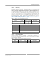
I2C Interface
2.15
!
The SC21 provides a USB-driven I2C interface on a 5-pin connector at the
connector PCB. See Figure 5, Position of I2C and touch interface connectors on
connector PCB for the connector’s exact position (with pin 1 indicated) - make sure
not to confuse it with the touch interface connector!
Table 16. I2C interface connector pin assignment
1
Pin
Name
1
SMBDATA_EXT
2
SMBCLK_EXT
3
SMBALERT_EXT#
4
AGND_A
5
Shield
Figure 5. Position of I2C and touch interface connectors on connector PCB
I2C interface
Touch interface
1
1
2.16
!
Touch Interface
The SC21 provides a USB-driven touch interface on a 4-pin connector at the
connector PCB. See Figure 5, Position of I2C and touch interface connectors on
connector PCB for the connector’s exact position (with pin 1 indicated) - make sure
not to confuse it with the I2C interface connector!
Table 17. Touch interface connector pin assignment
2.16.1
Pin
Name
1
USB Vcc
2
USB D-
3
USB D+
4
USB GND
Serial Interface via SA-Adapter (optional)
As an option, the board offers the possibility to provide a serial interface at the
connector PCB using a MEN standard SA-Adapter. This way, a serial interfaces can
be used which can be flexibly configured as needed, e.g., RS232 or RS422, isolated
or not, IBIS or GPS.
See MEN’s website for a list of SA-Adapters which can be used on the SC21.
Please contact MEN’s sales team for information about possible configurations
and special board versions.
MEN Mikro Elektronik GmbH
20SC21-00 E7 – 2012-10-04
33
Functional Description
2.17
Audio (optional)
The SC21 supports an optional high definition audio interface on the connector
PCB.
Table 18. Pin assignment of the HD audio interface
9
6
5
1
9
AUDIO_IN_R
5
AUDIO_SPDIF
8
AUDIO_GND
4
AUDIO_IN_L
7
AUDIO_OUT_R+
3
AUDIO_OUT_R-
6
AUDIO_OUT_L-
2
AUDIO_GND
1
AUDIO_OUT_L+
Table 19. Signal mnemonics of the HD audio interface
Signal
Description
AUDIO_EXT_OUT_L±/R± out
Line out, left and right, differential signal
pairs
AUDIO_EXT_IN_L/R
in
Line in, left and right
AUDIO_EXT_GND
-
Analog ground
AUDIO_EXT_SPDIF
out
S/PDIF output
MEN Mikro Elektronik GmbH
20SC21-00 E7 – 2012-10-04
Direction
34
Firmware Functions
3
Firmware Functions
The functions of the XC02BC board controller (BMC) and the XM01BC power and
display management controller (PMC) described in the following chapter depend on
the firmware. This user manual describes the functions as realized in the current
MEN standard firmware. To access the functions described below from own
applications, MEN provides the Windows Installset 13XM01-77 and the OSindependent MDIS driver packages, 13XM01-06 (BMC) and 13XC02-06 (PMC).
Please also refer to the general MDIS documentation for details.
3.1
Board Management Controller (BMC)
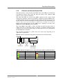
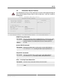
The SC21 is equipped with an intelligent internal power supply. Its onboard
microcontroller is used as a control and supervision device of the DC/DC converter,
the binary inputs of the SC21, its temperature and its display.
Additionally, it is used as a watchdog for the CPU and the microcontroller itself.
The device name of the watchdog is xm01bc_1 and the corresponding driver is
13XM01-06.
The microcontroller is connected to the CPU via SMBus. It is able to keep the
power supply active even if the external on/off-signal goes inactive. The
microcontroller controls the reset signal to be able to reset the CPU.
Windows XP Embedded, the pre-installed operating system of the SC21, needs a
controlled power down sequence. The power supply of the CPU can be kept active
via the SMBus even when the external on/off signal of the SC21 is inactive so that a
controlled power down of the operating system is possible. For further information
see Chapter 3.3.7.1 Off Delay on page 42.
Figure 6. Microcontroller block diagram
Voltage Supervision
Temperature Supervision
A/D Converter
SMBus
SMB Slave
Binary Inputs
In/Out Control
Control
Timer
MEN Mikro Elektronik GmbH
20SC21-00 E7 – 2012-10-04
Control Out
35
Firmware Functions
3.1.1
Available Functions
The BMC supports the following functions:
•
•
•
•
•
Board power sequencing control
Voltage and temperature supervision
System watchdog
Software reset functionality
Error state logging
3.2
Power and Display Management Controller (PMC)
The internal power supply unit’s microcontroller is also used as a watchdog for the
SC21 system. The device name of the watchdog is xc02_1 and the corresponding
driver is 13XC02-06.
It is possible to enable/disable the watchdog by the SMBus command
XC02C_WDOG_STATE. After the XC02C_STATUS byte (see Table 28, SMBus
commands for shutdown delay, on page 41) signals a shutdown, the watchdog is
disabled by the firmware. The watchdog is triggered by cyclic SMBus commands
(XC02C_WDOG_TRIG) from the CPU. The time interval between trigger
commands is configurable via the SMBus command XC02C_WDOG_TOUT (see
Table 23, SMBus commands XC02C_WOT_L / XC02C_WOT_H, on page 38). The
time interval is set to its maximum value after SC21 power up and the watchdog is
disabled. In case of a missing trigger unit’s microcontroller resets the complete
system. The number of missing SMBus trigger command exceptions is incremented
and can be read via the SMBus command XC02C_WDOG_ERR.
After three exceptions, the microcontroller switches off the power output (Vout) and
switches off the display. After a watchdog reset, the microcontroller waits for the
SMBus On acknowledge signal before it restarts the watchdog timer (depending on
the settings - see Chapter 3.3.5 SMBus On Acknowledge on page 39 for details).
Table 20. SMBus commands for the watchdog function
Name
Data
Range
Type
Description
XC02C_WDOG_STATE
0x05
0x00,
0x01
r/w
Watchdog state
XC02C_WDOG_TRIG
0x06
0
w
Watchdog trigger
signal
XC02C_WDOG_TOUT
0x07
0x01..
0xFF
r/w
Watchdog timeout
in 100ms steps
XC02C_WDOG_ERR
0x08
0x00..
0x04
r
Number of missing
on watchdog
trigger signals
MEN Mikro Elektronik GmbH
20SC21-00 E7 – 2012-10-04
Command
Code
36
Firmware Functions
Table 21. SMBus command XC02C_WDOG_TOUT
Value
Watchdog Timeout
1
100 ms
2
200 ms
3
300 ms
...
255
3.2.1
25.5 s (default)
Available Functions
The PMC supports the following functions:
•
•
•
•
•
•
Power up/down supervision
Adjustable power up wake on time
Watchdog functionality
Binary I/O access
Temperature and voltage monitoring
Brightness control
MEN Mikro Elektronik GmbH
20SC21-00 E7 – 2012-10-04
37
Firmware Functions
3.3
SMBus Functionality
3.3.1
SMBus Interface
The SC21’s internal power supply supports SMBus slave device functionality. The
7-bit SMBus address of the power supply unit is 0x09. Its microcontroller behaves
according to the SMBus Specification Version 2.0. The supported SMBus
commands and their functions are explained in the following chapters. The
commands are listed by their unique name. The "Data Range" column lists the valid
range of the data byte for the specific command code. The "Type" column specifies
the data direction for the specific command. 'r' specifies that the host can read the
data using the SMBus read-byte protocol. 'w' means the host can write data using
the SMBus write-byte protocol.
3.3.2
Wake On Time
The SC21 can be switched on/off by a programmable timer. The timer is included in
the internal power supply unit’s microcontroller and is programmable by the CPU
via SMBus commands (see Table 22, SMBus commands for wake on time function,
on page 38).
The behavior after power up by wake on time is identical to the behavior after power
up by key input. After the first wake on time event, the wake on time feature is
disabled.
Note: For the timer functionality it is necessary that the DC/DC converter and the
microcontroller are active, i.e. the power supply unit is connected to the DC/
DC converter, which is supplied with power. The SC21 will consume approx.
800 mW in this state.
Table 22. SMBus commands for wake on time function
Name
Command
Code
Data
Range
Type
Description
XC02C_WOT_L
0x00
0x00..
0xFF
r/w
Wake on time low byte
XC02C_WOT_H
0x01
0x00..
0xFF
r/w
Wake on time high byte
The wake on time delay can be configured via SMBus in a 16 bit counter to provide
the range according to the following table:
Table 23. SMBus commands XC02C_WOT_L / XC02C_WOT_H
Minimum
0 (OFF)
(default)
Maximum
Description
65,535 min
XC02C_WOT_L and XC02C_WOT_H build a
(45d 12h 15m) 16 bit value which represents the time in minutes
A user application that shall switch on the SC21 on a given date and time needs to
calculate the amount of minutes between shutdown and desired wake time.
MEN Mikro Elektronik GmbH
20SC21-00 E7 – 2012-10-04
38
Firmware Functions
3.3.3
Status of Binary Inputs
The status of the binary inputs is also signaled via SMBus commands. See Table 24,
SMBus commands for binary inputs status, on page 39.
Table 24. SMBus commands for binary inputs status
Name
XC02C_IN
Command
Code
0x0E
Data
Range
0x00..
0x1F
Type
r
Description
State of binary inputs
The binary inputs represent the status of the key input and the 4 geographical
address inputs that allow a user application to find out, e.g., where in a train an
SC21 is located.
3.3.4
Key Input
One of the binary inputs serves as an on/off input. When this signal is passive (open)
during power up of the input voltage, the system is not supplied with power. When
this signals goes active, the microcontroller switches the power supply to provide
the system with power. Regardless of the key input signal, the DC/DC converter and
the microcontroller are always supplied with power when the input voltage is
connected.
!
Note that key input functionality is only available when using a customized power
supply, as the key input signal from the included external power supply is always
active.
3.3.4.1
Key Input On
The microcontroller switches on the system power whenever the debounced state of
the key binary input switches from low to high state (On event). The microcontroller
debounces the key input in the following way: if the input is stable for 250ms, the
input state is interpreted.
3.3.5
SMBus On Acknowledge
The microcontroller provides an SMBus On Acknowledge feature. This feature is
enabled by using mode 1 to 11 according to Table 26, SMBus On acknowledge
timer modes, on page 40. The default mode is 0 (feature disabled, no SMBus
Acknowledge required). If enabled and the microcontroller does not receive a
SMBus On acknowledge during the configurable SMBus On Acknowledge delay,
the microcontroller resets the complete system by activating the reset output. The
number of missing SMBus acknowledge exceptions is incremented and can be read
via SMBus command XC02C_ONACK_ERR.
After reset is released, the acknowledge timer is restarted and the microcontroller
waits for SMBus acknowledge. After three exceptions the microcontroller disables
the power output Vout and switches off the display. After a power up of the SC21,
the On Acknowledge configuration is reset.
MEN Mikro Elektronik GmbH
20SC21-00 E7 – 2012-10-04
39
Firmware Functions
Table 25. SMBus commands for On acknowledge function
Command
Code
Name
Data
Range
Type
Description
XC02C_ONACK
0x02
0
w
On acknowledge
XC02C_ONACK_TOUT
0x03
0x00..
0x0B
r/w
On acknowledge
timeout
XC02C_ONACK_ERR
0x04
0x00..
0xFF
r
Number of missing
On acknowledges
Table 26. SMBus On acknowledge timer modes
Mode
SMBus On Acknowledge
0
Feature disabled = no acknowledge required (default)
1
1s
2
2s
3
4s
4
8s
5
16 s
6
32 s
7
64 s
8
128 s
9
256 s
10
512 s
11
1024 s
3.3.6
Shutdown
3.3.6.1
Shutdown by Software
At any time it is possible to shut down the power supply by software via SMBus
command XC02C_SWOFF. A shutdown by software is caused when an SMBus byte
write of 0x09 (command) and 0xA8 (magic value to avoid unintended shutdowns)
is done to the microcontroller’s address.
Table 27. SMBus command for shutdown by software function
Name
XC02C_SWOFF
3.3.6.2
Command
Code
0x09
Data
Range
0xA8
(magic)
Type
w
Description
Signal a software power
off from application
Shutdown by Key Input
When using a customized power supply, it is possible at any time to shut down the
power supply by switching off the key input. A shutdown by key input follows the
shutdown sequence.
MEN Mikro Elektronik GmbH
20SC21-00 E7 – 2012-10-04
40
Firmware Functions
3.3.7
Shutdown Delay
During the shutdown sequence the microcontroller provides a programmable
shutdown delay. The default state of the shutdown delay after power up of the SC21
is 0 (disabled). The shutdown delay is configurable via the SMBus command
XC02C_DOWN_DELAY, see Table 28, SMBus commands for shutdown delay, on
page 41 and Table 30, SMBus command XC02C_DOWN_DELAY, on page 41. The
shutdown delay timer is started after shutdown event. At any time during the
shutdown delay the shutdown sequence can be stopped by an On event (key input
on). The system is in running state then and the shutdown delay timer is cleared.
Table 28. SMBus commands for shutdown delay
Command
Code
Name
Data
Range
Type
Description
XC02C_DOWN_DELAY
0x0B
0x00..
0x07
r/w
Shutdown delay
XC02C_STATUS
0x0D
0x00..
0x01
r
Signal PSU status
to application
Table 29. SMBus command XC02C_STATUS
Bit
0
1
2..7
Value
Description
0
Shutdown event not signaled
1
Signal shutdown event
0
Normal operation
1
Display in protect state
(over/under-voltage or temperature)
0
Reserved
Table 30. SMBus command XC02C_DOWN_DELAY
Value
0
0 min
1
1 min
2
2 min
3
4 min
4
8 min
5
16 min
6
32 min
7
64 min
MEN Mikro Elektronik GmbH
20SC21-00 E7 – 2012-10-04
Shutdown Delay
41
Firmware Functions
3.3.7.1
Off Delay
During the shutdown sequence the microcontroller provides a programmable Off
delay. As default this feature is not enabled (mode 0). In this case there will be no
Off delay, the supply will be switched off immediately. When enabled (mode 1…5),
the microcontroller starts the Off delay timer after signaling the shutdown event to
the CPU. After timeout the microcontroller switches off the supply voltage (Vout).
Vout is kept disabled for at least 1 s, even if an immediate On event occurs. This
guarantees a proper power on reset of the supplied system. The Off delay can be
programmed using the SMBus command XC02C_OFF_DELAY, for details see
Table 31, SMBus command for Off delay function, on page 42 and Table 32,
SMBus command XC02C_OFF_DELAY, on page 42.
Table 31. SMBus command for Off delay function
Command
Code
Name
XC02C_OFF_DELAY
0x0C
Data
Range
Type
0x00..
0x05
r/w
Description
Off delay
Table 32. SMBus command XC02C_OFF_DELAY
Mode value
Off Delay
0
Feature off (no Off delay, default)
1
1 min
2
2 min
3
4 min
4
8 min
5
16 min
3.3.7.2
Off Acknowledge
The microcontroller provides a possibility to acknowledge the shutdown. It is
possible at any time during Off delay to shut down the power supply by the SMBus
command XC02C_OFFACK.
Table 33. SMBus command for Off acknowledge function
Name
XC02C_OFFACK
MEN Mikro Elektronik GmbH
20SC21-00 E7 – 2012-10-04
Command
Code
0x0A
Data
Range
0
Type
w
Description
Signal Off acknowledge
42
Firmware Functions
3.3.8
Voltage Supervision
Input and output voltage are supervised by the microcontroller. The microcontroller
supervises the 5V output voltage of the SC21’s internal DC/DC converter by
applying it through a voltage divider to one ADC channel. The supervision ranges
are set by the commands XC02C_VOLT_HIGH and XC02C_VOLT_LOW. These
values are written with MDIS descriptors and are not to be changed during normal
operation. When the voltage is exceeding this range, the SC21 goes into reset.
The output voltage is measured using the microcontroller internal ADC function.
The ADC value which represents the output voltage can be read via the SMBus
command XC02C_VOLT (see Table 34, SMBus command for voltage supervision
function, on page 43. With an ADC reference voltage of 3.00 volts the returned
value from this command is to be interpreted as
ADC
U mon = ------------- x3000mV
255
so that for example a returned value of 0xD5 corresponds to (0xD5/255)*3000 mV
= 2.506 V. This value results from the voltage divider tap between a 10k and 2.7k
resistor (factor 0.212), so the real output voltage of the DC/DC converter is 2.506 V/
0.212 = 11.8 V. This would be a typical output under load.
Table 34. SMBus command for voltage supervision function
Name
Command
Code
Data
Range
Type
Description
XC02C_VOLT
0x14
0x00..
0xFF
r
DC/DC output (voltage
divider factor = 0,212)
XC02C_VOLT_LOW
0x22
0x00..
0xFF
r/w
Minimum allowed
display supply voltage
XC02C_VOLT_HIGH
0x21
0x00..
0xFF
r/w
Maximum allowed
display supply voltage
3.3.9
Temperature Supervision
The microcontroller is able to determine the temperature inside the SC21. The CPU
can read the current temperature via the SMBus command XC02C_TEMP. This is
independent from the temperature sensor and supervision functionality of the
SC21’s embedded system core itself.
The temperature supervision is carried out by the temperature sensor LM50. The
LM50 is a precision integrated-circuit temperature sensor that can sense a -40°C to
+125°C temperature range. It converts its temperature to an analog voltage
according to the formula below:
OUTPUT
Vout=(10mV/°C x Temp °C) + 500 mV
Vout=+1.750mV at +125°C
Vout=+750mV at +25°C
Vout=+100mV at -40°C
MEN Mikro Elektronik GmbH
20SC21-00 E7 – 2012-10-04
43
Firmware Functions
This voltage is also converted as explained in Chapter 3.3.8 Voltage Supervision, but
directly attached to the ADC channel since it is within the maximum ADC range of
3,000 V. The Table 36. Temperature representation shows some values (which are
derived by (Vout/3000 mV) x 0xFF).
Table 35. SMBus commands for temperature supervision
Name
Command
Code
Data
Range
Type
Description
XC02C_TEMP
0x12
0x00..
0xFF
r
Converted
temperature
XC02C_TEMP_LOW
0x18
0x00..
0xFF
r/w
Minimum
temperature value
XC02C_TEMP_HIGH
0x13
0x00..
0xFF
r/w
Maximum
temperature value
The default values are -10 to +60° and can be changed at MEN depending on the
display type.
!
When changing these settings manually do not exceed the panel’s maximum
operating temperature range of -30 to +70°C!
Table 36. Temperature representation
Value
Temperature
0x22
-10°C
0x2a
0°C
0x55
+50°C
3.3.10
Display Backlight Power and Brightness Control
The microcontroller can control the display’s backlight brightness and switch the
display backlight power on and off (i.e., to prevent display operation outside its
specified temperature ranges).
The brightness is controlled using a PWM that can be adjusted in 0.5% steps by
using values from 0x00 to 0xC8 (0 to 200).
The XC02C_INIT_DS command is used to control whether the display is switched
on immediate after power on or whether it remains dark until the user application
switches it on with a XC02C_SW_DISP command. This "silent boot" feature allows
application testing and entering values in the BIOS of the onboard CPU. When the
application is deployed, the initial display state can be set to off so that BIOS and
OS boot messages do not appear in the field.
MEN Mikro Elektronik GmbH
20SC21-00 E7 – 2012-10-04
44
Firmware Functions
Table 37. SMBus commands for display control
Command
Code
Name
Data
Range
Type
Description
XC02C_SET_BR
0x17
0x00..
0xC8
r/w
Set/get brightness level
XC02C_SW_DISP
0x20
0x00..
0x01
r/w
Switch display on (1)
or off (0)
XC02C_BR_SRC
0x19
0x00..
0x01
r/w
Brightness source:
SMB command = 0
Photo diode = 1
XC02C_INIT_DS
0x25
0x00..
0x01
r/w
Initial display state
at powerup:
on = 0
off = 1
3.3.11
Optional Autonomous Brightness Control with Photo
Diode
When the SC21 is equipped with a photo diode for light detection the firmware
allows to pass brightness control to it. The command XC02C_BR_SRC switches
control from brightness setting with the SMB command XC02C_SET_BR to
autonomous setting. In this case the value is updated every 5s so short coverages of
the diode don't affect brightness.
To keep the same version of the firmware for all SC21 variants, its also possible to
switch to autonomous brightness control when there no photo diode is present. In
that case the brightness will always stay the same.
3.3.12
Miscellaneous Commands
The firmware supports some commands that are useful to retrieve information about
the build date and time.
With each call to the command XC02C_TIMESTAMP the firmware returns one
character of the build timestamp string that is stored in the microcontroller’s internal
EEPROM. This helps to identify the firmware version. The values returned are
concatenated in the MDIS driver and logged when the MDIS device that represents
the microcontroller is opened.
The command XC02C_ID returns a fixed value 0xC2 that is used to identify the
underlaying carrier board type. See Table 38, SMBus commands for PSU ID and
firmware revision number, on page 45.
Table 38. SMBus commands for PSU ID and firmware revision number
Name
Data
Range
Type
Description
XC02C_ID
0xFE
0xC2
r
Fixed firmware ID
XC02C_TIMES
TAMP
0x20
0x00..
0x01
r
Build date string, one
character at a time
MEN Mikro Elektronik GmbH
20SC21-00 E7 – 2012-10-04
Command
Code
45
BIOS
4
BIOS
4.1
Main Menu
Phoenix - AwardBIOS CMOS Setup Utility
+=======================================+======================================+
|
|
|
|
|
|
| > Standard CMOS Features
| > Frequency/Voltage Control
|
|
|
|
|
|
|
| > Advanced BIOS Features
|
Load Fail-Safe Defaults
|
|
|
|
|
|
|
| > Advanced Chipset Features
|
Load Optimized Defaults
|
|
|
|
|
|
|
| > Integrated Peripherals
|
Set Password
|
|
|
|
|
|
|
| > Power Management Setup
|
Save & Exit Setup
|
|
|
|
|
|
|
| > PnP/PCI Configurations
|
Exit Without Saving
|
|
|
|
|
|
|
| > PC Health Status
|
|
|
|
|
|
|
|
|
|
|
|
|
|
|---------------------------------------+--------------------------------------|
| Esc : Quit
^ v > <
: Select Item
|
| F10 : Save & Exit Setup
|
|------------------------------------------------------------------------------|
|
|
|
|
+==============================================================================
The ">" character in front of a menu item means that a sub-menu is available. An
"x" in front of a menu item means that there is a configuration option which needs to
be activated through a higher configuration option before being accessible.
MEN Mikro Elektronik GmbH
20SC21-00 E7 – 2012-10-04
46
BIOS
4.2
Standard CMOS Features
Phoenix - AwardBIOS CMOS Setup Utility
Standard CMOS Features
+=====================================================+========================+
|
Date (mm:dd:yy)
Mon, Jan 23 2008
|
Item Help
|
|
Time (hh:mm:ss)
10 : 57 : 22
|------------------------|
|
| Menu Level
>
|
| > IDE Channel 0 Master
[ None]
|
|
| > IDE Channel 0 Slave
[ None]
|
|
|
|
|
|
|
|
|
Base Memory
640K
|
|
|
Extended Memory
2086912K
|
|
|
Total Memory
2087936K
|
|
|
|
|
|
|
|
+=====================================================+========================+
F5: Previous Values
F6: BIOS Default Values
F7: Last Saved Values
Date (mm:dd:yy)
Description
Change the day, month, year and century.
Options
mm
Month
dd
Day
yy
Year
Time (hh:mm:ss)
Description
Change the internal clock.
Options
hh
Hours
mm
Minutes
ss
Seconds
MEN Mikro Elektronik GmbH
20SC21-00 E7 – 2012-10-04
47
BIOS
IDE Channel 0/1 Master/Slave — Sub-menu
IDE HDD Auto-Detection
[Press Enter]
IDE Channel 0 Master
Access Mode
[Auto]
[Auto]
Capacity
0 MB
Cylinder
Head
Precomp
Landing Zone
Sector
0
0
0
0
0
IDE HDD Auto-Detection
Description
Auto-detects the HDD's size, head etc. on this channel.
Options
None
IDE Channel 0/1 Master/Slave
Options
None
Manual
Auto
Access Mode
Options
CHS
Large
LBA
Auto
Capacity / Cylinder / Head / Precomp / Landing Zone / Sector
Options
None
Base Memory / Extended Memory / Total Memory
Description
MEN Mikro Elektronik GmbH
20SC21-00 E7 – 2012-10-04
You cannot change any values in the Memory fields. They are only
for information.
48
BIOS
4.3
Advanced BIOS Features
Phoenix - AwardBIOS CMOS Setup Utility
Advanced BIOS Features
+=====================================================+========================+
| > CPU Feature
[Press Enter]
|
Item Help
|
| > Hard Disk Boot Priority
[Press Enter]
|------------------------|
|
CPU L1 & L2 Cache
[Enabled]
| Menu Level
>
|
|
Hyper-Threading Technology[Enabled]
|
|
|
Quick Power On Self Test [Enabled]
|
|
|
First Boot Device
[Hard Disk]
|
|
|
Second Boot Device
[ZIP100]
|
|
|
Third Boot Device
[LS120]
|
|
|
Boot Other Device
[Enabled]
|
|
|
LAN-Boot ROM
[Disabled]
|
|
|
Boot Up NumLock Status
[On]
|
|
|
Security Option
[Setup]
|
|
| x APIC Mode
[Enabled]
|
|
|
MPS Version Control For OS[1.4]
|
|
|
OS Select For DRAM > 64MB [Non-OS2]
|
|
|
HDD S.M.A.R.T Capability [Disabled]
|
|
|
Full Screen LOGO Show
[Disabled]
|
|
|
Summary Screen Show
[Disabled]
|
|
|
|
|
|
|
|
|
|
|
+=====================================================+========================+
F5: Previous Values
F6: BIOS Default Values
F7: Last Saved Values
CPU Feature — Sub-menu
Thermal Management
Limit CPUID MaxVal
C1E Function
CPU C State Capability
On-Demand TCC
Execute Disable Bit
Virtualization Technology
[Thermal Monitor 2]
[Disabled]
[Disabled]
[Disabled]
[Disabled]
[Enabled]
[Enabled]
Thermal Management
Description
Shows the active thermal management.
Options
Thermal Monitor 1
On die throttling
Thermal Monitor 2
Ratio & VID transition
TM1 + TM2 enabled
Disabled
Limit CPUID MaxVal
Description
Set Limit CPUID MaxVal to 3, should be disabled for WinXP
Options
Disabled
Enabled
C1E Function
Description
Enables the Enhanced Halt State for power saving
Options
Disabled
MEN Mikro Elektronik GmbH
20SC21-00 E7 – 2012-10-04
Auto
49
BIOS
CPU C State Capability
Description
User can select the lowest C state supported according to CPU
and MB
Options
Disabled
C2
C4
C6
On-Demand TCC
Description
When enabled, it indicates the clock on to clock off interval ratio.
Options
Disable
50.0%
12.5%
62.5%
25.0%
75.0%
37.5%
87.5%
Execute Disable Bit
Description
When disabled, forces the XD feature flag to always return 0.
Options
Enabled
Disabled
Virtualization Technology
Description
When enabled, a VMM can utilize the addional hardware capabilities provided by Vanderpool Technology. (Not available for
SC21 versions with the Atom Z510P/PT processor.)
Options
Enabled
Disabled
Hard Disk Boot Priority — Sub-menu
1.
2.
3.
2.
USB-HDD0 : Intel Value SSD
USB-HDD1 : Intel Value SSD
USB-HDD2 : SanDisk Cruzer Micro
Bootable Add-in-Cards
Boot priority [Dynamic]
Description
Selects the boot device priority of any hard disk recognized.
Options
Dynamic
New detected devices are added to the end of
the boot-list.
Manual
The chosen setting is saved as long as the HDD
configuration of the system is not changed. (This
setting is advantageous if there is no battery in
the system).
Fixed
The BIOS scans the IDE controller and always
fixes the boot sequence:
1. HDD from 1st controller
2. HDD from 2nd controller
3. USB-HDD devices
MEN Mikro Elektronik GmbH
20SC21-00 E7 – 2012-10-04
50
BIOS
CPU L1 & L2 Cache
Description
Allows to enable or disable the processor cache memory.
You should disable cache only if absolutely necessary, e.g. for testing purposes, since this slows down the system considerably.
Options
Enabled
Disabled
Hyper-Threading Technology
Description
Enabled for Windows XP and Linux 2.4.x (OS optimized for Hyper
Threading Technology) and Disable for other OS (OS not optimized
for Hyper Threading Technology). (Not available for SC21 versions
with the Atom Z510P/PT processor.)
Options
Enabled
Disabled
Quick Power On Self Test
Description
Allows the system to skip certain tests while booting. This will
decrease the time needed to boot the system.
Options
Enabled
Disabled
First Boot Device / Second Boot Device / Third Boot Device
Description
Selects your boot device priority.
Options
LS120
ZIP100
USB-CDROM
Hard Disk
USB-FDD
Legacy LAN
CDROM
USB-ZIP
Disabled
Boot Other Device
Description
Selects your boot device priority.
Options
Enabled
Disabled
LAN-Boot ROM
Description
1x: The option ROM for PXE1 LAN boot is called once, then the
boot procedure continues with the normal boot order.
Endless: The option ROM for PXE LAN boot is called until it is successful, i.e. until an operating system is booted over LAN
(This function is available as of BIOS version 1.11; the special BIOS
version with RAID support does not support network boot.)
Options
Disabled
Endless
1x
1
Preboot Execution Environment. PXE provides a way for a system to initiate a network
connection to various servers prior to loading an OS. This network connection supports a
number of standard IP protocols such as DHCP and TFTP, and can be used for purposes
such as software installation and system inventory maintenance.
MEN Mikro Elektronik GmbH
20SC21-00 E7 – 2012-10-04
51
BIOS
Boot Up NumLock Status
Description
Selects power on state for NumLock.
Options
Off
On
Security Option
Description
Selects whether the password is required every time the system
boots or only when you enter setup.
Options
Setup
System
APIC Mode
Description
APIC mode extends the number of available IRQs (up to 23 IRQs)
for operating systems which can use this (Windows XP/2000).
Options
Enabled
MPS Version Control For OS
Description
Selects the multiprocessor specification (MPS) revision.
Options
1.4
1.1
OS Select For DRAM > 64MB
Description
Select OS2 only if you are running an OS/2 operating system with
greater than 64MB of RAM on the system.
Options
Non-OS2
OS2
HDD S.M.A.R.T Capability
Description
Enables the hard disk drive S.M.A.R.T capability. The Self Monitoring Analysis And Reporting technology monitors the hard disk's
condition and allows early prediction and warning of the hard disk
failing.
In order to use S.M.A.R.T you have to enable it and keep the
S.M.A.R.T.-aware hardware monitoring utility running in the background all the time.
Options
Disabled
Enabled
Full Screen LOGO Show
Description
Reserved to select between boot logos.
Options
Disabled
Summary Screen Show
Description
Show summary screen
Options
Enabled
MEN Mikro Elektronik GmbH
20SC21-00 E7 – 2012-10-04
Disabled
52
BIOS
4.4
!
Advanced Chipset Features
You should make changes in this menu only if you have thorough knowledge of
your system! Setting wrong values in this section may cause the system to
malfunction!
Phoenix - AwardBIOS CMOS Setup Utility
Advanced Chipset Features
+=====================================================+========================+
|
DRAM Timing Selectable
[By SPD]
|
Item Help
|
|
System BIOS Cacheable
[Enabled]
|------------------------|
|
Video BIOS Cacheable
[Disabled]
| Menu Level
>>
|
|
|
|
|
|
|
|
** VGA Setting **
|
|
|
On-Chip Frame Buffer Size [8MB]
|
|
|
Boot Type
[LVDS]
|
|
|
LCD Panel Type
[1024x768 generic]
|
|
|
Panel Scaling
[Auto]
|
|
|
BIA Control
[VBIOS Default]
|
|
|
TV Feature
Press Enter
|
|
|
|
|
+=====================================================+========================+
F5: Previous Values
F6: BIOS Default Values
F7: Last Saved Values
DRAM Timing Selectable
Description
Sets the method by which the DRAM timing is selected. If By SPD
is selected, the values for the following five items are configured
from the contents of the SPD (Serial Presence Detect) device.
Options
By SPD
System BIOS Cacheable
Description
Selecting Enabled allows caching of the system BIOS ROM at
0xF0000 to 0xFFFFF, resulting in better system performance.
Options
Enabled
Disabled
Video BIOS Cacheable
Description
Selecting Enabled allows caching of the video BIOS ROM at
0xC0000 to 0xCFFF, resulting in better video performance.
Options
Enabled
Disabled
VGA — On-Chip Frame Buffer Size
Description
Controls the pre-allocated memory for frame buffer
Options
1MB
8MB
4 MB
MEN Mikro Elektronik GmbH
20SC21-00 E7 – 2012-10-04
53
BIOS
VGA — Boot Type
Description
Selects the video device that will be activated during POST
Options
VBIOS Default
SDVO
LVDS
VGA — LCD Panel Type
Description
Selects the LCD panel used by the internal graphics device by
selecting the appropriate setup item. Some panels are not numbered due to size constraints
Options
640x480 generic
1024x600 TMD 5.61"
800x600 generic
1024x600 Samsung 4.8"
1024x768 generic
1024x768 Samsung 15"
640x480 NEC 8.4 "
1024x768 Sharp 7.2"
800x480 NEC 9"
1280x800 Samsung 15.4
VGA — Panel Scaling
Description
Controls the type of panel scaling
Options
Auto
VGA — BIA Control
Description
Selects BIA control and aggressiveness level through this setup
item
Options
VBIOS Default
MEN Mikro Elektronik GmbH
20SC21-00 E7 – 2012-10-04
54
BIOS
4.5
Integrated Peripherals
Phoenix - AwardBIOS CMOS Setup Utility
Integrated Peripherals
+=====================================================+========================+
| > On-Chip IDE Device
[Press Enter]
|
Item Help
|
| > Onboard Device
[Press Enter]
|------------------------|
| > PCI Express Root Port Func[Press Enter]
| Menu Level
>
|
| > USB Device Setting
[Press Enter]
|
|
|
|
|
|
|
|
+=====================================================+========================+
F5: Previous Values
F6: BIOS Default Values
F7: Last Saved Values
On-Chip IDE Device — Sub-menu
IDE HDD Block Mode
On-Chip Primary PCI IDE
IDE Primary Master PIO
IDE Primary Slave PIO
IDE Primary Master UDMA
IDE Primary Slave UDMA
Delay for HDD (Secs)
[Enabled]
[Enabled]
[Auto]
[Auto]
[Auto]
[Auto]
[0]
IDE HDD Block Mode
Description
If your IDE hard drive supports block mode, select Enabled for
automatic detection of the optimal number of block read/writes
per sector the drive can support.
Options
Enabled
Disabled
On-Chip Primary PCI IDE
Description
The integrated peripheral controller contains an IDE interface
with support for two IDE channels. Select Enabled to activate
each channel.
Options
Enabled
Disabled
IDE Primary Master/Slave PIO
Description
These fields allow your system hard disk controller to work faster.
Rather than have the BIOS issue a series of commands that
transfer to or from the disk drive, PIO (Programmed Input/Output) allows the BIOS to communicate with the controller and
CPU directly.
The system supports five modes, numbered from 0 to 4, which
primarily differ in timing. When Auto is selected, the BIOS will
select the best available mode.
Options
Auto
Mode 1
Mode 3
Mode 0
Mode 2
Mode 4
IDE Primary Master/Slave UDMA
Description
MEN Mikro Elektronik GmbH
20SC21-00 E7 – 2012-10-04
These fields allow your system to improve disk I/O throughput to
up to 100MB/s with the Ultra DMA/100 feature.
55
BIOS
Options
Auto
Disabled
UDMA66
UDMA100
UDMA33
Delay for HDD
Description
This feature allows users to set a higher delay for HDD detection
Options
0-15 seconds
Onboard Device — Sub-menu
Intel HD Audio Controller
USB Client Controller
Watchdog
Onboard LAN 1 Controller
[Auto]
[Enabled]
[Disabled]
[Enabled]
Intel HD Audio Controller
Description
Enables/disables the audio controller.
Options
Auto
Disabled
USB Client Controller
Description
Enables/disables the USB client controller.
Options
Enabled
Disabled
Watchdog
Description
If the watchdog is active the system will be rebooted after the
configured time when no application triggers the watchdog
Options
Disabled
1 min
2 min
5 min
10 min
15 min
20 min
30 min
Onboard LAN 1 Controller
Description
Enables/disables the onboard LAN controller by setting this item
to the desired value.
Options
Enabled
Disabled
PCI Express Root Port Func — Sub-menu
PCI Express Port 1
PCI Express Port 2
[Auto]
[Auto]
PCI Express Port 1/2
Description
Controls the activity of the PCI Express ports.
Options
Enabled
Disabled
Auto
MEN Mikro Elektronik GmbH
20SC21-00 E7 – 2012-10-04
56
BIOS
USB Device Setting — Sub-menu
USB
USB
USB
USB
USB
1.0 Controller
2.0 Controller
Operation Mode
Keyboard Function
Storage Function
[Enabled]
[Enabled]
[High Speed]
[Enabled]
[Enabled]
***USB Mass Storage Device Boot Setting***
Intel Value SSD 2.00
[Auto Mode]
Intel Value SSD 2.00
[Auto Mode]
SanDisk Cruzer Micro 0.1 [Auto Mode]
USB 1.0 Controller
Description
Enables/disables the Universal Host Controller interface for USB.
Options
Enabled
Disabled
USB 2.0 Controller
Description
Enables/disables the Enhanced Host Controller interface for
USB.
Options
Enabled
Disabled
USB Operation Mode
Description
Auto-selects USB device operation mode
Options
High Speed
If the USB device is a high speed device, it
operates in high-speed mode. If the USB
device is a full/low-speed device, it operates
in full/low speed mode
Full/Low Speed
All USB devices operate on full/low speed
mode.
USB Keyboard Function
Description
Enables/disables the USB Keyboard Function.
Options
Enabled
USB Storage Function
Description
Enables/disables the legacy support of USB Mass Storage
Options
Enabled
Disabled
Intel Value SSD 2.00/SanDisk Cruzer Micro 0.1
Description
Selects the boot up type for the USB SSD
Options
Auto mode
According to contents of USB mass storage
device
FDD mode
USB mass storage device boots up as floppy
disk
HDD mode
USB mass storage device boots up as hard
disk
MEN Mikro Elektronik GmbH
20SC21-00 E7 – 2012-10-04
57
BIOS
4.6
Power Management Setup
Phoenix - AwardBIOS CMOS Setup Utility
Power Management Setup
+=====================================================+========================+
|
Power-Supply Type
[AT]
|
Item Help
|
|
ACPI Function
[Enabled]
|------------------------|
|
ACPI Suspend Type
[S3(STR)]
| Menu Level
>
|
|
Soft-Off by PWR-BTTN
[Instant-Off]
|
|
|
PWRON After PWR-Fail
[On]
|
|
|
ATX_PWRGD Failure Mode
[Check at Startup]
|
|
| > HPET Feature
[Press Enter]
|
|
| > Intel DTS Feature
[Press Enter]
|
|
|
|
|
+=====================================================+========================+
F5: Previous Values
F6: BIOS Default Values
F7: Last Saved Values
Power-Supply Type
Description
Selects the type of power supply.
Options
AT
ATX
ACPI Function
Description
Enables/disables support of ACPI (Advance Configuration and
Power Interface).
Options
Enabled
ACPI Suspend Type
Description
Selects the ACPI state used for System Suspend.
Options
S3(STR)
Activates "Suspend To RAM" function.
Soft-Off by PWR-BTTN
Description
This field defines the power-off mode when using an ATX power
supply. The Instant-Off mode allows powering off immediately upon
pressing the power button. In the Delay 4 Sec. mode, the system
powers off when the power button is pressed for more than four
seconds or enters the suspend mode when pressed for less than 4
seconds.
Options
Instant-Off
Delay 4 Sec.
PWRON After PWR-Fail
Description
Sets the system power status when power returns to the system
from a power failure situation.
Options
Former-Sts
MEN Mikro Elektronik GmbH
20SC21-00 E7 – 2012-10-04
On
Off
58
BIOS
ATX_PWRGD Failure Mode
Description
Determines the system behaviour in case of a failure at the ATX
power good signal.
Options
Check at start up
Check always
HPET Feature — Sub-menu
HPET Support
[Enabled]
HPET Support
Description
Enables/disables the high-precision event timer in the chipset.
Options
Enabled
Disabled
Intel DTS Feature — Sub-menu
Intel DTS Function
x DTS Active temperature
x Passive Cooling Trip Point
x Passive TC1 Value
x Passive TC2 Value
x Passive TSP Value
Critical Trip Point
[Enabled]
55°C
95°C
2
0
10
POR
Intel DTS Function
Description
Enables/disables Intel DTS Function.
Options
Enabled
Disabled
DTS Active temperature/Passive Cooling Trip Point/Passive TC1
Value/Passive TC2 Value/Passive TSP Value
Description
These values are read-only values as monitored by the system
when the Intel DTS Feature is enabled.
Options
None
Critical Trip Point
Description
This value controls the temperature of the ACPI Critical Trip
Point; i.e. the point at which the operating system will shut down
the system.
Options
POR (POR =
100°C)
15°C
23°C
31°C
39°C
47°C
55°C
63°C
71°C
79°C
87°C
95°C
103°C
111°C
119°C
127°C
MEN Mikro Elektronik GmbH
20SC21-00 E7 – 2012-10-04
59
BIOS
4.7
PNP/PCI Configurations
Phoenix - AwardBIOS CMOS Setup Utility
PnP/PCI Configurations
+=====================================================+========================+
|
Init Display First
[Onboard]
|
Item Help
|
|
Reset Configuration Data [Disabled]
|------------------------|
|
| Menu Level
>
|
|
Resources Controlled By
[Auto(ESCD)]
|
|
| x IRQ Resources
[Press Enter]
|
|
|
|
|
|
PCI/VGA Palette Snoop
[Disabled]
|
|
|
PCI Latency Timer(CLK)
[ 32]
|
|
|
|
|
|
** PCI Express relative items **
|
|
|
Maximum Payload Size
[128]
|
|
|
|
|
+=====================================================+========================+
F5: Previous Values
F6: BIOS Default Values
F7: Last Saved Values
Init Display First
Description
Selects which graphics controller the system initializes when the
system boots.
Options
PCI Slot
Onboard
Reset Configuration Data
Description
Select Enabled to reset Extended System Configuration Data
(ESCD) when you exit Setup if you have installed a new add-on and
the system reconfiguration has caused such a serious conflict that
the OS cannot boot. Disabled is the default.
Options
Enabled
Disabled
Resources Controlled By
Description
BIOS can automatically configure all the boot and Plug&Play compatible devices. If you choose Auto, you cannot select IRQ, DMA
and memory base address fields, since BIOS automatically assigns
them.
Options
Auto(ESCD)
Manual
IRQ Resources
Description
MEN Mikro Elektronik GmbH
20SC21-00 E7 – 2012-10-04
When resources are controlled manually, you must assign each
system interrupt a type depending on the type of device using the
interrupt, i.e. either a PCI/ISA Plug&Play device (default) or a Legacy ISA device.
60
BIOS
PCI/VGA Palette Snoop
Description
Some non-standard VGA display cards may not show colors properly. This field allows you to set whether or not MPEG ISA/VESA
VGA cards can work with PCI/VGA. When this field is enabled, a
PCI/VGA can work with an MPEG ISA/VESA VGA card. When this
field is disabled, a PCI/VGA cannot work with an MPEG ISA/VESA
card.
Options
Enabled
Disabled
PCI Latency Timer (CLK)
Description
This BIOS feature controls how long a PCI device can hold the PCI
bus before another takes over. The longer the latency, the longer
the PCI device can retain control of the bus before handing it over
to another PCI device.
Normally, the PCI Latency Timer is set to 32 cycles. This means the
active PCI device has to complete its transactions within 32 clock
cycles or hand it over to the next PCI device.
For better PCI performance, a longer latency should be used, but a
long latency can also reduce performance as the other PCI devices
queuing up may be stalled for too long. The optimum latency time
depends on your system configuration.
Options
Decimal value between 0 and 255
Maximum Payload Size
Description
Sets the maximum TLP payload size for the PCI Express devices.
The unit is byte.
Options
128
MEN Mikro Elektronik GmbH
20SC21-00 E7 – 2012-10-04
61
BIOS
4.8
PC Health Status
Phoenix - AwardBIOS CMOS Setup Utility
PC Health Status
+=====================================================+========================+
|
Current System Temp
41°C
|
Item Help
|
|
Current CPU1 Temperature
38°C
|------------------------|
|
| Menu Level
>
|
|
|
|
|
|
|
|
|
|
+=====================================================+========================+
F5: Previous Values
F6: BIOS Default Values
F7: Last Saved Values
Current System Temp/Current CPU1 Temperature
Description
4.9
These values are read-only values as monitored by the system.
Frequency/Voltage Control
Phoenix - AwardBIOS CMOS Setup Utility
Frequency/Voltage Control
+=====================================================+========================+
|
Spread Spectrum
[Enabled]
|
Item Help
|
|
XPD Clock
[Disabled]
|------------------------|
|
| Menu Level
>
|
|
|
|
|
|
|
+=====================================================+========================+
F5: Previous Values
F6: BIOS Default Values
F7: Last Saved Values
Spread Spectrum
Description
Sets the value of the spread spectrum. If enabled, this setting
improves CE behavior.
Options
Disabled
Enabled
XPD Clock
Description
Enables the clock for the debug connector
Options
Disabled
MEN Mikro Elektronik GmbH
20SC21-00 E7 – 2012-10-04
Enabled
62
BIOS
4.10
Load Fail-Safe Defaults
If this option is selected, a verified factory setup is loaded.
On the first BIOS setup configuration, this loads safe values for setup, which make
the board boot up. This state is achieved again when the board is reprogrammed
with the necessary parameters using the related Flash program.
4.11
Load Optimized Defaults
At the moment this option has the same effect as described for Load Fail-Safe
Defaults.
If required, this option can be used to load optimized values, e.g. for the board to
boot faster. These values have to be defined in the BIOS binary by the BIOS
manufacturer. A special BIOS version is needed for this.
4.12
Set Password
This lets you set a password. Please note that this often leads to problems, since
passwords are easily forgotten.
4.13
Save & Exit Setup
This option saves the settings made and exits setup.
4.14
Exit without Saving
This exits setup without saving any settings.
MEN Mikro Elektronik GmbH
20SC21-00 E7 – 2012-10-04
63
Organization of the Board
5
Organization of the Board
To install software on the board or to develop low-level software it is essential to be
familiar with the board’s address and interrupt organization.
5.0.1
Processor View of the Memory Map
The memory map is allocated dynamically and may vary depending on the system
configuration.
Table 39. Memory map – processor view
Address Range
0xFDF00000..0xFDF7FFFF
Video controller (VGA-compatible)
0xD8000000..0xDFFFFFFF
Video controller (VGA-compatible)
0xFDFC0000..0xFDFDFFFF
Video controller (VGA-compatible)
0xFDFFF000..0xFDFFFFFF
USB (Universal Serial Bus)-Controller
0xFDFF8000..0xFDFFBFFF
Microsoft UAA bus driver for High Definition
Audio
0xFDB00000..0xFDBFFFFF
PCI standard-PCI-to-PCI-bridge
0xFDE00000..0xFDEFFFFF
PCI standard-PCI-to-PCI-bridge
0xFDBC0000..0xFDBDFFFF
Intel(R) 82574L Gigabit Network Connection #3
0xFDBFC000..0xFDBFFFFF
Intel(R) 82574L Gigabit Network Connection #3
0xFDD00000..0xFDDFFFFF
PCI standard-PCI-to-PCI-bridge
0xFDC00000..0xFDCFFFFF
PCI standard-PCI-to-PCI-bridge
0xFDFFE000..0xFDFFE3FF
Standard extended PCI-to-USB universal host
controller
0xFED00000..0xFED003FF
High precision event timer
0xFED00000..0xFED003FF
System board
0xFFB80000..0xFFBFFFFF
Intel(R) 82802 firmware hub
0xE0000000..0xEFFFFFFF
Motherboard resources
0x0000..0x9FFFF
System board
0xFEC00000..0xFEC00FFF
System board
0xFED13000..0xFED1DFFF
System board
0xFED20000..0xFED8FFFF
System board
0xFEE00000..0xFEE00FFF
System board
0xFFB00000..0xFFB7FFFF
System board
0xFFF00000..0xFFFFFFFF
System board
0xA0000..0xBFFFF
PCI bus
0xA0000..0xBFFFF
VGASave
0xC0000..0xDFFFF
PCI bus
0xE0000..0xEFFFF
PCI bus
MEN Mikro Elektronik GmbH
20SC21-00 E7 – 2012-10-04
Function
64
Organization of the Board
Address Range
Function
0xE0000..0xEFFFF
System board
0xF0000..0xFFFFF
PCI bus
0xF0000..0xFFFFF
System board
0x100000..0x1F5DFFFF
System board
0x1F5E0000..0x1F5FFFFF
System board
0x1F600000..0x1F6FFFFF
System board
0x1F700000..0xFEBFFFFF
PCI bus
5.0.2
I/O Memory Map
Table 40. Memory map - I/O
Address Range
0x00000000..0x00000CF7
PCI bus
0x00000000..0x00000CF7
DMA controller
0x00000010..0x0000001F
Motherboard resources
0x00000020..0x00000021
Programmable interrupt controller
0x00000022..0x0000003F
Motherboard resources
0x00000040..0x00000043
System timer
0x00000044..0x0000005F
Motherboard resources
0x00000061..0x00000061
Standard speaker sound
0x00000062..0x00000063
Motherboard resources
0x00000065..0x0000006F
Motherboard resources
0x00000070..0x00000073
System CMOS/real time clock
0x00000074..0x0000007F
Motherboard resources
0x00000080..0x00000090
DMA controller
0x00000091..0x00000093
Motherboard resources
0x00000094..0x0000009F
DMA controller
0x000000A0..0x000000A1
Programmable interrupt controller
0x000000A2..0x000000BF
Motherboard resources
0x000000C0..0x000000DF
DMA controller
0x000000E0..0x000000EF
Motherboard resources
0x000000F0..0x000000FF
Numerical coprocessor
0x00000170..0x00000177
Secondary IDE channel
0x000001CE..0x000001CF
VgaSave
0x000001F0..0x000001F7
Primary IDE channel
0x00000274..0x00000277
ISAPnP data read port
0x00000279..0x00000279
ISAPnP data read port
0x000002E8..0x000002EF
VgaSave
0x00000376..0x00000376
Secondary IDE channel
MEN Mikro Elektronik GmbH
20SC21-00 E7 – 2012-10-04
Function
65
Organization of the Board
Address Range
Function
0x000003B0..0x000003BB
VgaSave
0x000003C0..0x000003DF
VgaSave
0x000003F6..0x000003F6
Primary IDE channel
0x000004D0..0x000004D1
Motherboard resources
0x00000880..0x0000088F
Motherboard resources
0x00000900..0x000009BF
Motherboard resources
0x00000A79..0x00000A79
ISAPnP data read port
0x00000D00..0x0000FFFF
PCI bus
0x0000D000..0x0000DFFF
PCI standard-PCI-to-PCI-bridge
0x0000E000..0x0000EFFF
PCI standard-PCI-to-PCI-bridge
0x0000EF00..0x0000EF1F
Intel(R) 82574L Gigabit Network Connection #3
0x0000FB00..0x0000FB0F
Standard dual channel PCI-IDE controller
0x0000FC00..0x0000FC1F
Standard PCI-to-USB universal host controller
0x0000FD00..0x0000FD1F
Standard PCI-to-USB universal host controller
0x0000FE00..0x0000FE1F
Standard PCI-to-USB universal host controller
0x0000FF00..0x0000FF07
Video controller (VGA-compatible)
5.1
PCI Devices
Table 41. PCI Devices
Bus
Device
Number
0
0x00
0
Vendor ID
Device ID
0x0
0x8086
0x8100
Host bridge
0x02
0x0
0x8086
0x8108
Display Controller
0
0x1A
0x00
0x8086
0x8118
USB Client Controller
0
0x1B
0x00
0x8086
0x811B
HD Audio Controller
0
0x1C
0x00
0x8086
0x8110
PCI Express Root Port 1
0
0x1C
0x01
0x8086
0x8110
PCI Express Root Port 2
0
0x1D
0x00
0x8086
0x8114
USB UHCI Controller 1
0
0x1D
0x01
0x8086
0x8115
USB UHCI Controller 2
0
0x1D
0x02
0x8086
0x8116
USB UHCI Controller 3
0
0x1D
0x07
0x8086
0x8117
USB EHCI Controller
0
0x1F
0x00
0x8086
0x8119
LPC Controller
0
0x1F
0x01
0x8086
0x811A
IDE Controller
1
0x00
0x00
0x8086
0x10D3
Onboard Ethernet
Controller (on board versions with one PCI
Express link on the ESM
Express connector)
MEN Mikro Elektronik GmbH
20SC21-00 E7 – 2012-10-04
Device
Function
Function
66
Organization of the Board
5.2
SMBus Devices
Table 42. SMBus devices
Address
Function
0x12
XC02BC board controller (BMC1)
0x60
Protected register
0x6E
Protected register
0x98
Thermal sensor
0x9A
XM01BC board controller (BMC2)
0xA0
SPD data for system memory
0xAA
Configuration EEPROM for SC21
0xAC
Additional Configuration EEPROM for display computer data
0xD2 / 0xD3
Clock generator
5.3
Interrupt Mapping
Table 43. Interrupts
Interrupt
IRQ 0
High precision event timer
IRQ 8
High precision event timer
IRQ 9
Microsoft ACPI-conformal system
IRQ 11
Video controller (VGA-compatible)
IRQ 11
USB (Universal Serial Bus) controller
IRQ 13
Numerical coprocessor
IRQ 14
Primary IDE channel
IRQ 16
Microsoft UAA bus driver for High Definition Audio
IRQ 16
PCI standard-PCI-to-PCI-bridge
IRQ 16
Intel(R) 82574L Gigabit Network Connection #3
IRQ 16
Standard PCI-to-USB universal host controller
IRQ 17
PCI standard-PCI-to-PCI-bridge
IRQ 17
Standard PCI-to-USB universal host controller
IRQ 18
Standard PCI-to-USB universal host controller
IRQ 19
Standard extended PCI-to-USB universal host controller
MEN Mikro Elektronik GmbH
20SC21-00 E7 – 2012-10-04
Function
67
Appendix
6
Appendix
6.1
Literature and Web Resources
• SC21 data sheet with up-to-date information and documentation:
www.men.de/products/08SC21-.html
6.1.1
CPU
• Intel Processors
www.intel.com
6.1.2
SATA
• Serial ATA International Organization (SATA-IO)
www.serialata.org
6.1.3
USB
• USB:
Universal Serial Bus Specification Revision 1.0; 1996; Compaq, Digital Equipment Corporation, IBM PC Company, Intel, Microsoft, NEC, Northern Telecom
www.usb.org
6.1.4
Ethernet
• ANSI/IEEE 802.3-1996, Information Technology - Telecommunications and
Information Exchange between Systems - Local and Metropolitan Area Networks - Specific Requirements - Part 3: Carrier Sense Multiple Access with Collision Detection (CSMA/CD) Access Method and Physical Layer Specifications;
1996; IEEE
www.ieee.org
• Charles Spurgeon's Ethernet Web Site
Extensive information about Ethernet (IEEE 802.3) local area network (LAN)
technology.
www.ethermanage.com/ethernet/
• InterOperability Laboratory, University of New Hampshire
This page covers general Ethernet technology.
www.iol.unh.edu/services/testing/ethernet/training/
6.1.5
HD Audio
• Intel High Definition Audio:
www.intel.com/design/chipsets/hdaudio.htm
MEN Mikro Elektronik GmbH
20SC21-00 E7 – 2012-10-04
68
Appendix
6.1.6
PCI Express
• PCI Express Base Specification, Revision 1.0
April 29, 2002
PCI Special Interest Group
www.pcisig.com
6.1.7
PCI Express Mini Card
• PCI Express Mini Card Electromechanical Specification
Revision 1.2; October 26, 2007
PCI Special Interest Group
www.pcisig.com
6.2
Finding out the Product’s Article Number, Revision and
Serial Number
MEN user documentation may describe several different models and/or design
revisions of the SC21. You can find information on the article number, the design
revision and the serial number on two labels attached to the board.
• Article number: Gives the product’s family and model. This is also MEN’s
ordering number. To be complete it must have 9 characters.
• Revision number: Gives the design revision of the product.
• Serial number: Unique identification assigned during production.
If you need support, you should communicate these numbers to MEN.
Figure 7. Labels giving the product’s article number, revision and serial number
Complete article number
08SC21-00
00.00.00
Revision number
Serial number
MEN Mikro Elektronik GmbH
20SC21-00 E7 – 2012-10-04
69