1
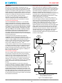
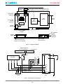
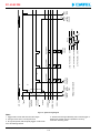
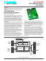
®
PC-414COM
®
DSP COMM Port Adapter
A/D Interface
FEATURES
• Adds a powerful A/D “front end” to DSP Array Processor
boards
• Up to 14MHz transfer rate (7 megasamples/second)
without loading host ISA bus
• Up to 10MHz A/D sample rates
• Mounts directly on DATEL’s PC-414 A/D board
• Pin-compatible with TI’s 320C40 COMM ports
• Offers full range of A/D options
A significant limitation to high-speed analog-to-digital (A/D)
converter performance on PC-compatible analog input boards
is the slow speed of the host ISA (Industry Standard
Architecture) bus. The PC-414COM adapter module avoids
these bus delays by sending A/D data directly from a host
DATEL PC-414 A/D board to an adjacent third party Digital
Signal Processor (DSP) board. The adapter connects to Texas
Instruments 320C40 series DSP’s using the “COMM” port
digital interface.
The COMM port is a fast, byte-wide port with transfer rates up
to 7 million samples per second on the PC-414COM. The host
PC-414 can collect data to its local FIFO memory at A/D
sampling rates up to 10MHz and includes a sample counter for
repeated frames of specified size. Or the system can run
“forever” with non-stop streaming A/D conversion. For A/D
sampling rates above about 7MHz, the PC-414 must briefly
stop periodically to allow the DSP to collect data.
The adapter is normally offered as an integrated set with its
PC-414 A/D carrier board and is ordered together under a
common model number. Existing PC-414’s in the field may be
modified by DATEL to accept the adapter.
Typical applications include all high-speed DSP A/D
conversion such as FFT’s (Fast Fourier Transforms), sonar,
digital filters, custom test systems, ultrasonics, high-speed
control loops, spectrometers, simulators, imaging, and speech
processing. The COMM port interface also has a more
powerful, subtle speed advantage for the DSP programmer.
Instead of having to retrieve the analog data from some slow
external bus interface, the A/D data is already “inside the DSP”
and can be used immediately or allowed to accumulate in the
PC-414 FIFO (First In, First Out) memory for a short time. This
non-bus high-speed transfer has a significant advantage for
Windows® applications.
The PC-414COM is a 3.5-inch by 4.375-inch daughter card
which mounts on the host PC-414 A/D board via corner
standoffs. The internal system consists of programmable logic
configured as a state machine controller. The integrated set of
boards occupy one slot width in the host PC. The adapter
takes A/D data from the PC-414’s 16-bit parallel data port and
reformats it for transmission through the byte-wide COMM port
to the DSP. The adapter also connects to the PC-414 parallel
digital I/O port for several control signals. These appear as I/O
bits on the ISA bus. Please refer to the PC-414 Data Sheet,
software diskettes, and User Manuals for full information on
this board.
Programming
Port
P2
P4
PC-414
Digital
I/O Port
P5
RST,
HF*
+5V
Mode
Control
40MHz
Oscillator
Word to Byte
Formatter
PC-414
Parallel
A/D Data
Inport
DSP COMM
Port Header
Connector
Handshake
Logic
16 data
XCLK
EF*
State Machine Controller
P3
8 data
CSTRB*
CRDY*
CREQ*
CACK*
(Alternate
Pinout)
P1
Figure 1. Functional Block Diagram
DATEL, Inc., Mansfield, MA 02048 (USA) • Tel: (508)339-3000, (800)233-2765 Fax: (508)339-6356 • Email: [email protected] • Internet: www.datel.com
105
®
®
PC-414COM
SPECIFICATIONS
Mounting Method
Unidirectional asynchronous
digital data interface between a
DATEL PC-414 data acquistion
board parallel data port and a type
“I” (input) 320C40 DSP “COMM”
port. The COMM port is the
receiver and the PC-414 interface
adapter is the transmitter. The
purpose is very high speed A/D
data transfers which are not
slowed down by the ISA bus.
The COMM port adapter is a small
daughter PC board attached to the
PC-414 using existing standoff
mounting holes already on the
PC-414. The COMM port adapter
attaches to both the existing parallel
data port and the digital I/O port.
One existing connector (P4 on the
PC-414 - the older parallel data
port) must be removed to fit the
PC-414COM adapter.
Outline Dimensions
3.5 inches x 4.375 inches
Number of Data Bits
8 (one COMM port)
Power Required
Data Rate
14 Megabytes per second
(7 megasamples/sec) typical
within a 4-byte burst.
+5Vdc power at 500mA max is
supplied from the PC-414 digital
I/O port (not from the parallel data
port).
COMM Port Connector
Token Assignment
The PC-414 COMM port adapter
is permanently assigned as a
type “O” (output) and will not
respond to direction changes. The
COMM adapter includes power up
“token forcer circuits” per TI’s
suggestions.
Data Format
Data is digitally multiplexed as
groups of 4 bytes containing two
12 to 16-bit A/D samples per 32bit longword. The Least Signficant
Byte is sent first. One full
longword (4 bytes, two A/D
samples) is always sent once the
first byte is started. See note 1.
Dual row right angle flat cable
male header, InterCon Systems
type 5654-015, 30 pins (2 x 15),
mounted beneath the adapter PC
board to avoid using more than
one PC slot. The COMM port PC
board is also pinned out in parallel
to an AMP P/N 104069-5 or a
Samtech TMS-1-10-01-T-D-RA.
When mounted in the host PC,
the COMM port connector faces
up (i.e., away from the PC’s
motherboard).
Number of Slots
One PC slot (PC-414 plus COMM
port adapter).
Flat Cable Length
The COMM port interface
assumes a receiving 320C40
board in an adjacent host PC slot.
The flat cable length for maximum
speed is 6 inches or less. Greater
length may degrade the speed
and/or fail to function.
Data Overflow
Standard status register and/or
ISA bus interrupt signals are
available on the PC-414 carrier
board to indicate FIFO overflow
(lost data).
PC-414 FIFO Size
4096 samples
(Typical at +25°C under dynamic conditions unless noted)
Function
Data Flow Control
Uses standard 320C40 CSTRB*/
CRDY* handshake protocol as
specified in the Texas Instruments
documentation. The byte transfers
use the following mode:
The CSTRB* output will remain
inhibited until the PC-414 A/D FIFO
memory is half full or greater. At
FIFO half full, the COMM port
interface will send four bytes (two
A/D samples) to the DSP receiver
using normal CSTRB*/CRDY*
handshaking then will inhibit
CSTRB* until FIFO half full occurs
again. If the FIFO is continuously
half full or greater, the interface will
send data as long as the DSP
accepts it. See Note 2.
Logic Controls
The COMM port will inhibit data
transfers when the PC-414 A/D
data FIFO is empty.
State Machine Reset
This is controlled from an output
bit on the PC-414 digital I/O port
or from P1-29. See Note 3.
Notes
1. Both CREQ* and CACK* have internal terminations as
shown and are used by the token forcer circuits. The
PC-414COM adapter is always the token owner.
2. In operation, the A/D FIFO will always store the last half
FIFO’s worth of data. The DSP can always get as much data
as it needs as long as the A/D continues sampling. If A/D
sampling stops, the last half FIFO may be read from the ISA
bus. In addition, the DSP can ignore the COMM port interface
by not responding with CRDY* even if the A/D continues
running.
3. A CAUXRES* input is not provided to the PC-414 COMM
port interface. This control normally resets the PC-414 and
the COMM port interface. However these functions are
available from the ISA bus register controls.
DATEL, Inc., Mansfield, MA 02048 (USA) • Tel: (508)339-3000, (800)233-2765 Fax: (508)339-6356 • Email: [email protected] • Internet: www.datel.com
106
®
®
PC-414COM
Applications
Data Format and Channel Synchronization
Since the PC-414COM adapter is downstream from the
PC-414’s FIFO on-board memory, the system can collect data
non-stop continuously to the DSP at high speed with no lost
samples. The architecture differs significantly from competitive
designs. Also the full range of triggering, sample clocking, and
channel addressing is available from the host PC-414. These
functions are controlled from the ISA bus and are normally set
up only once at the beginning of the A/D session.
Data is delivered to the COMM port in whatever format was
selected on the PC-414. Each A/D sample is right justified and
may be sign-extended on the PC-414. For multi-channel data,
the channel ordering is multiplexed with a typical 4-channel
data stream having the channel sequence: 0, 1, 2, 3, 0, 1, . . .
indefinitely. Therefore data must be demultiplexed (“unraveled”)
on the DSP side. For highest speed, there is no channel
address tagging to add overhead to the data stream, so DSP
software must not get out of sequence.
The DSP array processor board is typically placed in an
adjacent or nearby ISA slot with a short flat cable and
connector assembly. Refer to the specifications for details.
Some applications assign an unused analog channel to a
known DC voltage for positive channel synchronization. Also,
the PC-414 can use counted frames with an ISA I/O port
status indication and optional interrupt when a frame is
complete. Channel addressing always starts on channel zero
for the beginning of a frame therefore a reliable counting
algorithm will fully recover all channels. Since the trigger frame
timing, sample counter and FIFO flags on the PC-414 are all
independent, users should either fully empty the FIFO after
each frame (using the empty bit to verify) or reset the FIFO or
make absolutely sure your counting function does not lose
channel synchronization. Other applications may detect
excessive intersample differences to flag discontinuities as an
indication of lost samples.
Formatting and Handshaking
The PC-414COM adapter accepts two 12, 14, or 16-bit A/D
words and reformats them as four bytes to be sent across the
COMM port interface. The on-board logic handshakes with the
COMM port protocol and will automatically attempt to send bytes
if the adapter is ready. As long as the DSP responds to CSTRB*
outputs from the adapter with CRDY* handshakes, data will be
sent to the COMM port. Since the DSP completely controls this
handshaking, the DSP can accept data at the rate and amount
that it needs. Any data which is not immediately used will
accumulate in the PC-414 FIFO and will not be lost as long as it
is read before the FIFO overflows. The DSP can read a longword
at a time or initiate a burst.
Two A/D words are always formatted as four bytes for
compatibility with the 32-bit longword architecture of the
COMM port. The PC-414COM port is permanently assigned as
a type “O” (output) COMM port and will ignore change of
direction or token passing requests. The receiver DSP board
must be a type “I” input. The PC-414COM includes a token
forcer circuit to initialize the C40 to an “I” input.
Start
➀
Collect A/D
data to FIFO
Yes
A FIFO overflow condition sets an ISA bus maskable interrupt
or status flag. Full ISA bus controls can inhibit the A/D at any
time, reset the FIFO and start again. In addition, the OUT0
parallel port bit (P5-20) will clear the state machine controller
when low. The DSP receiver can program the COMM port in
DMA or program transfer mode.
DSP
needs more
data?
FIFO
>half full?
No
No
Exit
The Last Block of Samples
Yes
Since the controller inhibits transfers below FIFO half full, the
very last group of samples, after the A/D has permanently
stopped, may be read from the FIFO using the ISA bus (after
switching PC-414 Command Register bit 6 to ZERO).
Assert CSTRB*
The PC-414COM works well with signal streaming where the
A/D either runs continuously or at regular on/off periods in
counted blocks. These applications usually have a bandwidth
problem and therefore need a high speed COMM port
interface.
No
CRDY*
asserted?
For lower speed applications or ones with very short A/D
sequences, these will not activate the COMM port interface until
the A/D FIFO is at least half full (2049 samples). Thus there will
be an initial delay at first before data reaches the DSP. And
samples will be left in the FIFO at the end of the session. The
beginning delay is primarily a data skewing issue, taken care of
by properly indexing the data. The data which is still in the FIFO
after A/D sampling stops must be removed by ISA bus access.
Or leave the A/D running long enough to deliver all needed data
then discard the last half FIFO.
Repeat four
times
(one longword)
Yes
Transfer 1 byte.
Deassert CSTRB*
Note ➀ - A/D sampling continues non-stop
during COMM port transfers
Figure 2. PC-414COM Flow Diagram
DATEL, Inc., Mansfield, MA 02048 (USA) • Tel: (508)339-3000, (800)233-2765 Fax: (508)339-6356 • Email: [email protected] • Internet: www.datel.com
107
®
®
PC-414COM
PROGRAMMING
P1 CONNECTOR
Normally, software provided by the Array Processor board
supplier will completely control the COMM port from the DSP
side. Free low level software libraries are available from DATEL
to control the PC-414 or the PC-414SET program can be used.
The overall sequence of operation is to set up the host
interrupt systems, initialize the PC-414, prepare the DSP to
accept COMM port transfers then start A/D conversion on the
PC-414. The DSP may then retrieve A/D data indefinitely
without further programming the PC-414.
To set up the PC-414, program all registers normally except
that the Command Register bit 6 must be set to ONE to enable
the parallel data port connection to the COMM port adapter.
Note that A/D data may be steered to either the ISA bus or the
parallel/COMM port but not both simultaneously. These
selections are mutually exclusive.
Use two I/O writes with bit encoding to reset then run the
controller. Use this two-write sequence anytime that the
controller appears to be locked up, indicated by a loss of
control. After everything is initialized, enable A/D sampling in
the PC-414 Command Register.
After power up and any time the adapter controller is reset,
CSTRB* will not be asserted if the A/D clock is not running yet
and the trigger has not started gating A/D samples into the
FIFO.
Host system code should be running concurrently with the
DSP so that overflow (lost data) interrupts are processed from
the PC-414. In cases where the DSP is also the ISA bus
master, the DSP should periodically test for overflow status.
Please note that when the COMM port adapter is installed, the
FIFO must be 4096 samples.
This pad area accepts two 2-row 30 pin connectors (15 pins
per row) with different spacing between rows. There are three
rows total with equal spacing between the rows. The connector
types are either the Intercon Systems or AMP (see
specifications).
Pin 1, 31 - Data 0 Out
Pin 2 - Grounded via SG1
Pin 3, 32 - Data 1 Out
Pin 4 - Ground
Pin 5, 33 - Data 2 Out
Pin 6 - Ground
Pin 7, 34 - Data 3 Out
Pin 8 - Ground
Pin 9, 35 - Data 4 Out
Pin 10 - Ground
Pin 11, 36 - Data 5 Out
Pin 12 - Ground
Pin 13, 37 - Data 6 Out
Pin 14 - Ground
Pin 15, 38 - Data 7 Out
Pin 16 - Ground
Pin 17, 39 - CSTRB* Out
Pin 18 - Ground
Pin 19, 40 - CRDY* In
Pin 20 - Ground
Pin 21, 41 - CREQ*
Pin 22 - Ground
Pin 23, 42 - CACK*
Pins 24, 26, 28, 30 - Ground
Pins 25, 27, 43, 44 - No connection
Pin 29, 45 - CTOKRES* input with 10Kohm pullup to +5V. If J1
1-3 is closed, a LOW on this input resets the controller. If J1 13 is open, only the pullup remains. Note that controller reset is
fully controllable from the ISA bus if J1 1-2 is closed.
VERY IMPORTANT
The two inner rows of this 3-row connector (the two
rows away from the board edge) are connected in parallel.
P4 CONNECTOR
This pad area accepts a 2-row 20 pin connector. The
connector type is a Samtech TMS-1-10-01-T-D-RA (see
specifications).
Pin 1 - Ground
Pin 2 - Data 0 Out
Pin 3 - Ground
Pin 4 - Data 1 Out
Pin 5 - Ground
Pin 6 - Data 2 Out
Pin 7 - Ground
Pin 8 - Data 3 Out
Pin 9 - Ground
Pin 10 - Data 4 Out
Pin 11 - Ground
Pin 12 - Data 5 Out
Pin 13 - Ground
Pin 14 - Data 7 Out
Pin 15 - CREQ*
Pin 16 - Data 6 Out
Pin 17 - Ground
Pin 18 - CACK*
Pin 19 - CRDY* In
Pin 20 - CSTRB*
MISCELLANEOUS I/O BITS and JUMPERS
PC-414 Parallel port outbit 0 (I/O word BASE+2, bit 8):
0 = Reset internal state machine controller if J1 1-2 is
closed
1 = Run
Jumper J1 (use only one setting):
1-2 Reset state machine from I/O outbit 0 (see above)
1-3 Reset state machine from a LOW on P1-29
Connector P2:
For programming the internal state machine controller.
Make no connection.
Solder gap SG1:
Closing this gap grounds P1-2 and P1-4.
PAL changes:
The host PC-414 requires a change of its Programmable
Array Logic to provide FIFO empty and half full signals on
the P3 connector. Also, faster 0.3-inch DIP FIFO’s are
required.
CONNECTOR PINOUTS
The PC-414COM adapter is offered in 3 different COMM port
connector pinouts. Only one connector is installed. All pinouts
are shown component-side view. Silkscreening on the board
locates pin 1 which is also indicated with a square circuit pad.
DATEL, Inc., Mansfield, MA 02048 (USA) • Tel: (508)339-3000, (800)233-2765 Fax: (508)339-6356 • Email: [email protected] • Internet: www.datel.com
108
®
®
PC-414COM
Flat
Cable
DSP Array Processor Board (adjacent slot)
DSP COMM Port Connector (between boards)
(user supplied)
A/D Parallel
Data Port
P1/P4
P3
2 1 3
J1
1
Access Hole
for DIP
Switches
Analog
Inputs
A/D
Module
FIFO
A/D
Memory
Controller
Parallel
I/O Port
P5
PC-414 A/D Board
PC-414 COM
Adapter
Analog
Inputs
PC-414COM
Adapter
P1/P4
A/D Module
P3
Mounting
Standoffs
DSP COMM
Port Connector
PC-414 Carrier Board
(edge view, top chassis)
Figure 3. Configuration Diagram
Digital Outport on
PC-414 (I/O Base + 2)
15
Connector P5
8
0
RST*
2
1
3
Controller
1
31
+5V
J1
2
SG1
4
10kΩ
CSTRB* OUT
CRDY* IN
CREQ*
CACK*
CTOKRES* (Reset*)
17
19
21
23
29
39
40
41
42
45
30
P1 COMM
Port
To P4
Figure 4. I/O Terminations and Jumpering
DATEL, Inc., Mansfield, MA 02048 (USA) • Tel: (508)339-3000, (800)233-2765 Fax: (508)339-6356 • Email: [email protected] • Internet: www.datel.com
109
®
®
CRDY*
(to PC-414COM)
(from PC-414COM) CSTRB*
DATA
Timing is not to scale
FIFO
has 2049
samples
CRDY* IN
CSTRB* OUT
COMM Port
Data
ACQuire
<Half Full
>Half Full
FIFO Empty
Not Empty
Trigger
A/D Clock
Sampling
All
registers starts.
Begin
armed
frame.
➀
➁
See detail
➂
See detail
(from PC-414COM)
Transfer
4 bytes
See detail
Byte 0
Byte 1
72ns typ.
Sample Next
frame
count
reached. start
Stop A/D
➃
PC-414COM
Figure 5. System Timing Diagram
Notes
1. Trigger width must be less than the frame length.
4. ACQuire remains high indefinitely and no further trigger is
needed if the sample counter is disabled in non-stop,
continuous streaming mode.
2. Timing is shown with a non-stop A/D clock.
3. At high A/D speeds, half full rapidly toggles or will remain
true if the DSP lags behind.
DATEL, Inc., Mansfield, MA 02048 (USA) • Tel: (508)339-3000, (800)233-2765 Fax: (508)339-6356 • Email: [email protected] • Internet: www.datel.com
110
®
®
PC-414COM
PC-414COM Setup Instructions
8. Set up the DSP board to accept data from the PC-414. If
necessary, verify that the COMM port on the DSP side is truly
empty and inactive. Set up the PC’s interrupt system to accept
PC-414 interrupts, if used. Allocate PC memory and open files
as required. CAUTION: Incorrect DSP DMA programming can
lock up the DSP. Test the DSP COMM port in status mode
first.
1. Solder Gaps
Before installing the PC-414 board, verify that the solder gaps
are properly set on the non-component side of the board.
Using anti-static protection, hold the board with the
components facing away from you and the ISA bus connector
at the lower left. Solder gaps SG1 and SG2 are next to each
other in the top center of the board directly under a standoff
mounting hole. SG3 is at the top right, directly below the P3
connector.
9. If external triggering is desired, the PC-414 A/D Command
Register requires two writes. The first write sets external
triggering (bit 0=1) leaving the A/D temporarily still disabled
(bit 1=0) The second write to the Command Register sets bit
0=1 (again) and bit 1=1 to start the A/D. To avoid a mode
lockup, do not toggle both bits 0 and 1 with the same write.
Set the solder gaps as follows if not already done. Get
experienced assistance if you do not have excellent soldering
skills:
SG1 = Open.
SG2 = Closed.
For internal triggering, only one write to the Command
Register is needed. For either internal or external triggering,
carefully set all bits correctly. Set bit 6=1 to enable the parallel
data port on the last Command Register write.
This connects P3-17 to the “XFLAG” output on U5. XFLAG is
selected for the FIFO Empty Flag by special programming of
the PC-414COM PAL’s. A standard PC-414 does not have this
PAL programming.
Note that this is triggering, not A/D sample clocking.
The system should now be sending data to the DSP board
unless it is waiting for an external trigger. Optionally verify
progress by testing the ACQuire and FIFO empty flags in the
Status Register.
CAUTION - Do not close both SG1 and SG2 simultaneously.
SG3 = Closed. This connects the “XCLK” external handshake
clocking from the COMM port.
You may vary the above sequence as long as the A/D
Command Register is last (starts A/D conversion). DATEL
strongly recommends testing the PC-414 with data sent to the
ISA bus (bit 6=0) first to verify that everything else works.
Carefully examine the output data array from the FIFO. If your
code is not working, try DATEL’s PC-414SET diagnostic.
2. Set PC-414 SW2 DIP switches 4 and 5 both off. This
selects parallel port transfer mode 3 (external clocking). See
Figures 6.4 and 6.5 in the PC-414 User Manual. These
switches appear in a cutout in the middle of the COMM port
adapter.
10. When all data is taken, stop the A/D and reset the adapter.
3. COMM port Adapter settings: Set Jumper J1 on the COMM
port adapter to connect J1 1-2 (reset via I/O bit 8). Close P1SG1 on the adapter if desired for your required grounding. See
the P1 pinout in the PC-414COM data sheet.
For debugging purposes only, the former Busy Low output on
P3-11 is reassigned as FIFO Half Full* output for use with the
COMM port. This change is done by special PAL
reprogramming which is not available on a standard PC-414.
4. Review all other PC-414 switches and jumpers very
carefully according to the PC-414 User Manual then install the
board. Connect the COMM port cable to the DSP receiver
board. CAUTION: The adapter actively drives the outputs and
the receiver must be set up as a type “I” (input) device. The
adapter does not run in 3-state mode.
If you are debugging your own code, consider partly repeating
the programming above each time new data is taken for
diagnostics so that the system always starts in a known state.
Some final advice: In order to successfully pass data into the
A/D FIFO, five conditions must be met. Valid input signals must
reach all the way to the input terminals on the A/D converter
itself, the FIFO must not be full, the A/D sample clock must be
running, a trigger must have occurred and the A/D must be
enabled in the Command Register. In order for correct data to
be accumulated, many other conditions must be met including
sampling at Nyquist rates or better, not exceeding the input
range, preventing alias signals, remaining within the input
common mode range, reducing input noise, etc.
Programming Sequence
Properly programming the COMM port system requires correct
instruction sequences for four sections (the PC-414, the
receiving DSP board, the COMM port adapter and the host
PC). The philosophy here is to get the downstream items
prepared to accept data before the upstream devices.
5. Write a 0000h to the PC-414 Command Register to disable
the A/D section and parallel data port. This should occur by
default at power up. Program the PC-414 timers and all other
registers except the Command Register. Reset the
A/D FIFO.
In order to successfully pass data through the COMM port to
the DSP, the adapter controller must be in the “run” state, the
DSP must be properly programmed, the A/D FIFO must be
steered to the parallel port and the data cabling must be
perfect.
6. Reset the COMM port adapter by writing the PC-414 Digital
I/O Outport (I/O Base+2) with bit 8=0. Allow a small delay after
this write for the reset state to propagate through the controller.
Note that the I/O port should power up with bit 8=0 so you may
be able to skip this step if your testing shows high reliability.
7. Write the I/O Outport again with bit 8=1 (run).
DATEL, Inc., Mansfield, MA 02048 (USA) • Tel: (508)339-3000, (800)233-2765 Fax: (508)339-6356 • Email: [email protected] • Internet: www.datel.com
111
®
®
PC-414COM
ORDERING INFORMATION
(Adapter board only - requires modifications on PC-414 carrier board):
PC-414COM1
PC-414COM2
PC-414COM3
Intercon header connector (for Ariel)
AMP header connector (for Radisys Sonitech)
Samtech TMS-1-10-01-T-D-RA header
Please order only using the full board model numbering:
PC-414x2COMy
where “x” indicates the selected A/D option for the PC-414
A/D board, and “y” indicates the COMM port connector as indicated above.
Example: PC-414F2COM2
Please refer to the PC-414 data sheet. Note that model numbering is structured per
order.
PC-414 ORDERING INFORMATION
MODEL NUMBERING
PC-414
2
A/D Type, Channels, Resolution
A = 4 SSH chans., 12-bit
B = 4 chans., 14-bit
C = 4 chans., 12-bit
D = 1D chan., 12-bit
E = 16S/8D chans., 12-bit
F = 2 simul. chans., 12-bit
G = 2 simul. chans., 14-bit
H = 1D chan., 12-bit
J = 8 simul. chans., 12-bit
L = 16 simul. chans., 12-bit
M = 4 simul. chans., 16-bit
COM2
FIFO Memory Size
2 = 4,096 A/D samples
Use the 4k FIFO only
for the COMMport.
Input Polarity
A = Bipolar
B = Unipolar
Use this designator only
for G models requiring
polarity section.
COMM Port
Add for COMM port
interface
Example: PC-414F2COM2 Two simultaneous A/D’s, 2MHz, 12-bit resolution, 4,096 FIFO samples.
61-7342340
PC-490B
SMA male to BNC male coaxial cable, 1 meter length. (One cable required per channel)
DB-25 screw termination adapter, 25-pin for PC-414E, J, L.
Each board is power-cycle burned-in, tested, and calibrated. All models include a user manual. The warranty period is one
year. A QuickBASIC and low-level “C” library source disk is available on request at no charge.
For complete information see PC-414 data sheet.
Note: Software is not included with board. Please add to your order.
Windows is a Microsoft trademark
DATEL, Inc., Mansfield, MA 02048 (USA) • Tel: (508)339-3000, (800)233-2765 Fax: (508)339-6356 • Email: [email protected] • Internet: www.datel.com
112