1
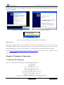
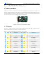
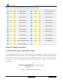
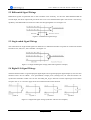
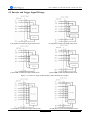
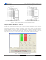
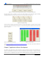
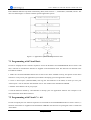
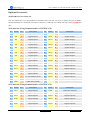
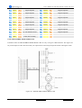
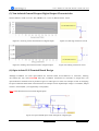
User’s Manual
For
Encoder Counter I/O Card
Version 1.0
©2006 All Rights Reserved
Attention: Please read this manual carefully before using the card!
Floor 3, Block 2, Nanyou Tianan Industry Park, Nanshan Dist, Shenzhen, China
Tel: (86)755-26434369
Fax: (86)755-26402718
URL: www.leadshine.com
E-Mail: [email protected]
Table of Contents
Chapter 1 General Information.................................................................................................................................... 1
1.1 Introduction ................................................................................................................................................... 1
1.2 Features ......................................................................................................................................................... 1
1.3 Specifications ................................................................................................................................................ 1
1.4 Environment .................................................................................................................................................. 2
1.5 Power Consumption ...................................................................................................................................... 2
1.6 Output Power for Each Encoder.................................................................................................................... 2
1.7 Dimension ..................................................................................................................................................... 2
1.8 Applications................................................................................................................................................... 2
Chapter 2 Installation .................................................................................................................................................. 2
2.1 Package Contents........................................................................................................................................... 2
2.2 Unpacking ..................................................................................................................................................... 3
2.3 Hardware Installation .................................................................................................................................... 3
Installation Procedures ...............................................................................................................................3
2.4 General Purpose Output Initial Level Setting................................................................................................ 3
2.5 Driver Install and Demo Software................................................................................................................. 4
Leadshine All-in-one CD............................................................................................................................4
Driver Installation.......................................................................................................................................4
Demo Software...........................................................................................................................................5
Chapter 3 Principles of Operation ............................................................................................................................... 5
3.1 Function Block Diagram ............................................................................................................................... 5
3.2 Encoder Feedback ......................................................................................................................................... 6
3.3 Trigger ........................................................................................................................................................... 6
Chapter 4 ENC7480/ENC7480-IO Connectors........................................................................................................... 7
4.1 Connector Distribution .................................................................................................................................. 7
4.2 X1 Connector................................................................................................................................................. 7
4.3 X2 Connector ( Using the ACC37-74ENC.) ................................................................................................. 8
4.4 X3 Connector ( Using the ACC37-74ENC.) ................................................................................................. 8
Chapter 5 Signal Connections ..................................................................................................................................... 9
5.1 Encoder and Trigger Signal Input Circuits .................................................................................................... 9
5.2 Differential Signal Wirings.......................................................................................................................... 10
5.3 Single-ended Signal Wirings ....................................................................................................................... 10
5.4 Digital I/O Signal Wirings........................................................................................................................... 10
5.5 Encoder and Trigger Signal Wirings............................................................................................................ 11
Chapter 6 ENC7480 Demo Software ........................................................................................................................ 12
Chapter 7 Application Software Development .......................................................................................................... 13
7.1 Programming with Visual Basic .................................................................................................................. 14
7.2 Programming with Visual C++ 6.0.............................................................................................................. 14
Chapter 8 Function Definitions ................................................................................................................................. 15
Chapter 9 Troubleshooting ........................................................................................................................................ 23
Chapter 10 Order Information ................................................................................................................................... 24
Optional Accessories ......................................................................................................................................... 25
Terminal Borad: ACC37ENC-GL ............................................................................................................25
I
User’s Manual for ENC7480 Encoder Counter I/O Card
Cable: DB37M-DB9F+MD4F+MD6F Cable...........................................................................................26
Appendix ................................................................................................................................................................... 27
(1) DLL Functions Quick List ........................................................................................................................... 27
(2) Connect to RENISHAW Touch Trigger Probes ........................................................................................... 27
(3) Non-isolated General Purpose Digital Output Characteristics..................................................................... 28
(4) Opto-isolated I/O Terminal Board Design ................................................................................................... 28
II
User’s Manual for ENC7480 Encoder Counter I/O Card
Chapter 1 General Information
1.1 Introduction
The ENC7480 is a PCI plug-and-play board that provides inputs and decoding for up to four incremental
quadrature encoders or linear scales. In addition, the ENC7480-IO has 32 general inputs and 32 general outputs.
Incremental quadrature encoders and linear scales are used to provide feedback signals from motors and actuators,
that is, to count rotations & linear movements and convert the physical movement into a series of electrical signals.
These signals are sent to the computer which then decides whether or not to trigger signals that control the motor’s
movement and what those control signals should be. The ENC7480/ENC7480-IO is the link between up to four
incremental quadrature encoders and the computer. They can be used for a wide range of measurement and motion
control applications, such as CNC machines, robotics and co-ordinate measuring machines.
The features of the ENC7480/ENC7480-IO are made accessible by using the functions provided in the
ENC7480.dll (for Windows 95/98/2000/XP). Enc7480 Demo assists the measurement system developer in
verifying and testing hardware systems.
1.2 Features
1)
High speed 32-bit PCI Bus, plug-and-play
2)
4 encoder inputs
3)
Quadrature Encoder input signal can be up to 6.5MHz (×4)
4)
Quadrature Encoder multiplier (×1, ×2, ×4)
5)
Zero input for each encoder channel
6)
32 general inputs
7)
32 general outputs (initial level settable)
8)
Counters can be read on the fly or be captured by triggers to be read later.
9)
Two trigger/capture signals optional (TR1,TR2)
10) Driver and DLL supports for Windows 95/98/2000/XP
11) Support VB/VC/LabVIEW programming tools
12) ENC7480 demo software for verifying and testing hardware systems
1.3 Specifications
1)
Number of channels: 4
2)
Input frequency: 6.5MHz (Max.) for Quadrature Encoder(×4); 3.93 MHz (Max.) for differential PUL/DIR
inputs; 2.42 MHz (Max.) for single-ended PUL/DIR inputs
3)
28 bit counters for each encoder channel. Counter range: -134,217,727~134,217,727 (28-bit)
4)
2 latch trigger signals optional and configurable
5)
Zero input for each encoder channel
Tel: +086 0755-26434369
Email: [email protected]
Page: 1/25
Web Site: www.leadshine.com
User’s Manual for ENC7480 Encoder Counter I/O Card
6)
32 general purpose digital inputs (Terminal board ACC37-74ENC: 3.3V @LVCMOS )
7)
32 general purpose digital outputs (Terminal board ACC37-74ENC: 10mA, 3.3V @LVCMOS )
8)
Output ports for LED and buzzer (Synchronous with TR1 or TR2)
1.4 Environment
1)
Operating temperature: 0℃~50℃
2)
Storage temperature: -20℃~80℃
3)
Humidity: 5%RH - 85%RH
1.5 Power Consumption
+5VDC±5% @ 900mA (Max)
Or +3.3VDC±5% @ 1500mA (Max)
1.6 Output Power for Each Encoder
5V±5% @ 100mA (Max)
1.7 Dimension
164mm (L) × 98.4mm (H)
1.8 Applications
1)
CMM Machines
2)
Process Monitoring
3)
Motion Control
4)
Scanner
5)
Other Position Measurement Systems
6)
I/O Extension
Chapter 2 Installation
This chapter describes how to install the ENC7480. The ENC7480 automatically configures the port and BIOS
addresses. It is not necessary to configure the addresses, hence avoiding addressing conflicts.
2.1 Package Contents
Besides this User's Manual, the package also includes the following items:
• ENC7480/ENC7480-IO Encoder Counter I/O Card
Tel: +086 0755-26434369
Email: [email protected]
Page: 2/29
Web Site: www.leadshine.com
User’s Manual for ENC7480 Encoder Counter I/O Card
• ACC37-74ENC Terminal Board (1 at least.)
• Cable37-2.0 (1 at least)
• 40-pin to 37-pin connector with bracket (Optional)
• Leadshine All-in-one CD
See “Order Information” section for more information about package contents.
If any of these items are missing or damaged, contact the dealer from whom you purchased the product or
Leadshine.
2.2 Unpacking
As with any electronic device, you should take care while handling to avoid damage from static electricity. Before
removing the ENC7480/ENC7480-IO from its packaging, ground yourself to eliminate any stored static charge.
The card contains electro-static sensitive components that can be easily damaged by static electricity. Therefore,
the card should be handled on a grounded anti-static mat. Inspect the card module carton for obvious damage.
Shipping and handling may cause damage to your module. Be sure there is no shipping and handling damage on
the carton before continuing.
Note: Do not attempt to install a damaged board in the computer.
2.3 Hardware Installation
The ENC7480 is equipped with Plug and Play PCI controllers. It can request base addresses according to PCI
standards. The system BIOS will install the system resources based on the PCI cards’ configuration registers and
system parameters (also can be set by the system BIOS). The ENC7480 can be inserted into any PCI slot without
any configuration modification to the system resources. Please note that the PCI system board and slot must
provide bus-mastering capabilities to operate at optimum level. See “Power Consumption” section in page 2.
Installation Procedures
1. Turn off your computer.
2. Remove the cover from your computer.
3. Before handling the PCI card, discharge any static buildup on your body by touching the metal case of the
computer. Hold the edge of the card and do not touch the components.
4. Set the jumpers on the ENC7480-IO card. See “General Purpose Output Initial Level Setting” section.
5. Select a 32-bit PCI slot.
6. Position the board into the PCI slot you have selected.
7. Secure the card in place at the rear panel of the system.
2.4 General Purpose Output Initial Level Setting
There are four jumpers (J1, J2, J3 and J4) on the board for setting the INITIAL LEVEL of general purpose outputs.
Tel: +086 0755-26434369
Email: [email protected]
Page: 3/29
Web Site: www.leadshine.com
User’s Manual for ENC7480 Encoder Counter I/O Card
Remember that the INITIAL LEVEL and jumpers settings are related to types of terminal board used. Consult
table 2-1 or table 2-2 and set these jumpers correctly before installing the ENC7480-IO. Default setting is all these
jumpers are short circuit.
Table 2-1: Using terminal board: ACC37-74ENC
Digital Output
Initial LEVEL is LOW
Initial LEVEL is HIGH
OUT1~8
J1 Short Circuit
J1 Open Circuit
OUT9~16
J2 Short Circuit
J2 Open Circuit
OUT17~24
J3 Short Circuit
J3 Open Circuit
OUT25~32
J4 Short Circuit
J4 Open Circuit
Table 2-2: Using terminal board: ACC37ENC-GL (Opto-isolated terminal board, 50mA@35V)
Digital Output
Initial LEVEL is HIGH
Initial LEVEL is LOW
OUT1~8
J1 Short Circuit
J1 Open Circuit
OUT9~16
J2 Short Circuit
J2 Open Circuit
OUT17~24
J3 Short Circuit
J3 Open Circuit
OUT25~32
J4 Short Circuit
J4 Open Circuit
2.5 Driver Install and Demo Software
Leadshine All-in-one CD
Please open the ENC7480 folder and you will see another four subfolders: “Drivers”, “Demo”, “Inf” and
“Documents”
“Drivers” folder: The folder includes driver for the ENC7480/ENC7480-IO.
“Inf” folder: The folder includes library functions files for ENC7480/ENC7480-IO.
“Demo” folder: The folder includes demo software for the ENC7480/ENC7480-IO.
“Documents” folder: The folder includes manual and datasheet of the ENC7480/ENC7480-IO.
Driver Installation
Windows 98 SE / ME / 2000 / XP Installation
1. Execute the “drive.exe” in the “Drivers” folder on the distribution CDROM.
2. Turn off your computer.
3. Remove the cover from your computer.
4. Set the jumpers on the ENC7480-IO (No jumper on the ENC7480).
5. Select a 32-bit PCI slot and handling the PCI card, and position the board into the PCI slot you have selected.
6. Secure the card in place at the rear panel of the system.
7. Power on your computer, and the system will display a form showing “Found New Hardware Wizard” when
enter the system. See Figure 2-1(a). Select “Yes, this time only” option to continue driver installation. See Figure
2-1(b).
8. Select “Install the software automatically (Recommended)” to finish installation. After finishing installation,
Tel: +086 0755-26434369
Email: [email protected]
Page: 4/29
Web Site: www.leadshine.com
User’s Manual for ENC7480 Encoder Counter I/O Card
the ENC7480 is ready to use. See Figure 2-1(c). Now, you can test it with ENC7480 demo software on the
distribution CDROM.
(a) Found new hardware
(b) Continue to install
(c) Finish installation
Figure 2-1: Driver installation (Take Windows XP for example.)
Demo Software
The demo software doesn’t need installation. Execute the “Enc7480.exe”, then you can test the
ENC7480/ENC7480-IO and your application system. It’s very helpful for verifying a motion control system
during the design phase of a project. See “Chapter 6” for more information about ENC7480 Demo software.
Check http://www.leadshine.com/News/en/e_news_detail1.asp?id=228 for the latest version software for the
ENC7480/ENC7480-IO.
Chapter 3 Principles of Operation
3.1 Function Block Diagram
Figure 3-1 is the function block diagram of the ENC7480/ENC7480-IO.
Figure 3-1: Function block diagram of the ENC7480/ENC7480-IO
Tel: +086 0755-26434369
Email: [email protected]
Page: 5/29
Web Site: www.leadshine.com
User’s Manual for ENC7480 Encoder Counter I/O Card
3.2 Encoder Feedback
The encoder counter has 28 bit resolution and may be read at any time. In A/B phase mode, the maximum count
rate is 6.5 MHz (×4). The ENC7480/ENC7480-IO can receive encoder feedback signals, including the EA, EB,
and EZ. Every channel has six pins for three differential pairs of phase-A (EA), phase-B (EB) and index (EZ)
input. A, B phases with sectors positioned 90 degrees out of phase, the two output channels of the quadrature
encoder indicate both position and direction of rotation. If A leads B, for example, the disk is rotating in a
clockwise direction. If B leads A, then the disk is rotating in a counter-clockwise direction. Up count when A
leads B, and down count when B leads A. EZ signal is called zero or index or reference signal, which supplies a
single pulse per revolution. This single pulse can be used to zero the counter value, and can be used for precise
determination of a reference position or a trigger signal to latch/capture counter value. For noise immunity or
applications where the encoder is positioned a significant distance from the ENC7480/ENC7480-IO, differential
encoder or using a quadruple complementary-output line driver (ie. 26LS31) to convert single-ended signal to
differential signal is recommended.
In PUL/DIR mode, the maximum count rate is 3.93 MHz for differential inputs and 2.42MHz for single-ended
inputs. The PUL (pulse) signal is connected to the EA+ and the DIR (direction) signal is connected to the EB+.
UP count and DOWN count are related to encoder feedback signal types. Differential inputs and PNP
single-ended inputs are UP count when DIR HIGH, see Figure 3-2(b); while NPN single-ended inputs are UP
count when DIR LOW, opposite with Figure 3-2(b).
Typically an encoder requires a +5 VDC power supply and ground reference, both of which are available from the
ENC7480/ENC7480-IO.
(a) A/B phase mode
(b) PUL/DIR mode (differential and PNP)
Figure 3-2: Encoder feedback signals
3.3 Trigger
The ENC7480 is able to capture all four encoder positions synchronised in hardware when trigger signal effective.
Captured data is placed in a register and may be retrieved by user software at any time before resetting the register.
The trigger input circuit designated trigger is an edge triggered input which can synchronously latch the counter
values.
Figure 3-3: Edge triggered input
Tel: +086 0755-26434369
Email: [email protected]
Page: 6/29
Web Site: www.leadshine.com
User’s Manual for ENC7480 Encoder Counter I/O Card
Chapter 4 ENC7480/ENC7480-IO Connectors
4.1 Connector Distribution
There are four connectors on the ENC7480-IO/ENC7480, namely the X1, the X2, the X3 and the X4. The X1 is
mainly for encoder input signals; the X2 and the X3 are for general purpose digital inputs and outputs; the X4 is
reserved for further use. See Figure 4-1. Please note that there is no 40 pin or 20 pin IDC male connectors on the
ENC7480 when it carried out from Leadshine, while the ENC7480-IO has.
Figure 4-1: Connectors of the ENC7480/ENC7480-IO
4.2 X1 Connector
X1 connector is a DB37 connector, it mainly includes encoder and trigger signals. Table 4-1 shows the detail
information about connector pins used ACC37-74ENC terminal board.
Table 4-1: X1 connector description (Terminal board: ACC37-74ENC)
No.
Name
I/O
Description
No.
Name
1
5V
O
+5V Output
20
GND
2
GND
+5V Output GND
21
EA2+
I
Encoder A(2) +
3
EA1+
I
Encoder A(1) +
22
EA2-
I
Encoder A(2) -
4
EA1-
I
Encoder A(1) -
23
EB2+
I
Encoder B(2) +
5
EB1+
I
Encoder B(1) +
24
EB2-
I
Encoder B(2) -
6
EB1-
I
Encoder B(1) -
25
EZ2+
I
Encoder Index(2) +
7
EZ1+
I
Encoder Index(1) +
26
EZ2-
I
Encoder Index(2) -
8
EZ1-
I
Encoder Index(1) -
27
TR2+
I
Trigger(2) +
9
TR1-
I
Trigger(1) -
28
TR2-
I
Trigger(2) -
10
5V
O
+5V Output
29
GND
11
GND
+5V Output GND
30
EA4+
I
Encoder A(4) +
12
EA3+
I
Encoder A(3) +
31
EA4-
I
Encoder A(4) -
13
EA3-
I
Encoder A(3) -
32
EB4+
I
Encoder B(4) +
14
EB3+
I
Encoder B(3) +
33
EB4-
I
Encoder B(4) -
15
EB3-
I
Encoder B(3) -
34
TR1+
I
Trigger(1) +
Tel: +086 0755-26434369
Email: [email protected]
Page: 7/29
I/O
Description
+5V Output GND
+5V Output GND
Web Site: www.leadshine.com
User’s Manual for ENC7480 Encoder Counter I/O Card
16
EZ3+
I
Encoder Index(3) +
35
EZ4-
I
Encoder Index(4) -
17
EZ3-
I
Encoder Index(3) -
36
BUF
O
Output Port for Buzzer
18
EZ4+
I
Encoder Index(4) +
37
LED
O
Output Port for Probe LED
19
5V
O
+5V Output
4.3 X2 Connector ( Using the ACC37-74ENC. See Chapter 9 for using the ACC37ENC-GL.)
X2 connector is a 40-Pin IDC header connector (male), it includes 16 digital inputs and 16 digital outputs.
Leadshine offers 40-Pin IDC to DB37 ribbon cable (20cm in length) with expansion plugboard for the “37 pin DB
2m” cable. The user can use the ACC37-74ENC terminal board for connections. Table 4-2 shows the detail
information about connector pins used ACC37-74ENC terminal board.
Table 4-2: X2 connector description (Terminal board: ACC37-74ENC)
Pin
Name
I/O
Description
Pin
Name
I/O
Description
1
IN1
I
Digital Input 1
20
GND
2
IN2
I
Digital Input 2
21
OUT1
O
Digital Output 1
3
IN3
I
Digital Input 3
22
OUT2
O
Digital Output 2
4
IN4
I
Digital Input 4
23
OUT3
O
Digital Output 3
5
IN5
I
Digital Input 5
24
OUT4
O
Digital Output 4
6
IN6
I
Digital Input 6
25
OUT5
O
Digital Output 5
7
IN7
I
Digital Input 7
26
OUT6
O
Digital Output 6
8
IN8
I
Digital Input 8
27
OUT7
O
Digital Output 7
9
IN9
I
Digital Input 9
28
OUT8
O
Digital Output 8
10
IN10
I
Digital Input 10
29
OUT9
O
Digital Output 9
11
IN11
I
Digital Input 11
30
OUT10
O
Digital Output 10
12
IN12
I
Digital Input 12
31
OUT11
O
Digital Output 11
13
IN13
I
Digital Input 13
32
OUT12
O
Digital Output 12
14
IN14
I
Digital Input 14
33
OUT13
O
Digital Output 13
15
IN15
I
Digital Input 15
34
OUT14
O
Digital Output 14
16
IN16
I
Digital Input 16
35
OUT15
O
Digital Output 15
17
3.3V
O
+3.3V Power Supply Output
36
OUT16
O
Digital Output 16
18
3.3V
O
+3.3V Power Supply Output
37
GND
19
GND
+3.3V Output GND
+3.3V Output GND
+3.3V Output GND
4.4 X3 Connector ( Using the ACC37-74ENC. See Chapter 9 for using the ACC37ENC-GL.)
X3 connector is a 40-Pin IDC header connector (male), it includes 16 digital inputs and 16 digital outputs.
Leadshine offers 40-Pin IDC to DB37 ribbon cable (20cm in length) with expansion plugboard for the “37 pin DB
2m” cable. The user can choose the ACC37-74ENC terminal board for connections. Table 4-3 shows the detail
information about connector pins used ACC37-74ENC terminal board.
Tel: +086 0755-26434369
Email: [email protected]
Page: 8/29
Web Site: www.leadshine.com
User’s Manual for ENC7480 Encoder Counter I/O Card
Table 4-3: X3 connector description (Terminal board: ACC37-74ENC)
Pin
Name
I/O
Description
Pin
Name
I/O
Description
1
IN17
I
Digital Input17
20
GND
2
IN18
I
Digital Input18
21
OUT17
O
Digital Output17
3
IN19
I
Digital Input19
22
OUT18
O
Digital Output18
4
IN20
I
Digital Input20
23
OUT19
O
Digital Output19
5
IN21
I
Digital Input21
24
OUT20
O
Digital Output20
6
IN22
I
Digital Input22
25
OUT21
O
Digital Output21
7
IN23
I
Digital Input23
26
OUT22
O
Digital Output22
8
IN24
I
Digital Input24
27
OUT23
O
Digital Output23
9
IN25
I
Digital Input25
28
OUT24
O
Digital Output24
10
IN26
I
Digital Input26
29
OUT25
O
Digital Output25
11
IN27
I
Digital Input27
30
OUT26
O
Digital Output26
12
IN28
I
Digital Input28
31
OUT27
O
Digital Output27
13
IN29
I
Digital Input29
32
OUT28
O
Digital Output28
14
IN30
I
Digital Input30
33
OUT29
O
Digital Output29
15
IN31
I
Digital Input31
34
OUT30
O
Digital Output30
16
IN32
I
Digital Input32
35
OUT31
O
Digital Output31
17
3.3V
O
+3.3V Power Supply Output
36
OUT32
O
Digital Output32
18
3.3V
O
+3.3V Power Supply Output
37
GND
19
GND
+3.3V Output GND
+3.3V Output GND
PC Power Ground
Chapter 5 Signal Connections
5.1 Encoder and Trigger Signal Input Circuits
The ENC7480/ENC7480-IO can accept encoder input from either differential or single-ended signals. The
ENC7480/ENC7480-IO uses 26LS32 line receivers to accept differential signals, including EA, EB, EZ, TR1 and
TR2. These signals must provide at least 3.5V across the differential pairs with at least 6 mA driving capability.
See Figure 5-1. Note that twisted-pair shielded cabling provides better immunity in electrically noisy
environments.
Figure 5-1: Differential signal input circuits
Tel: +086 0755-26434369
Email: [email protected]
Page: 9/29
Web Site: www.leadshine.com
User’s Manual for ENC7480 Encoder Counter I/O Card
5.2 Differential Signal Wirings
Differential signals are preferred due to their excellent noise immunity. To drive the ENC7480/ENC7480-IO
encoder input, the driver output must provide at least 3.5V across the differential pairs with at least 6 mA driving
capability. The GROUND level of the two sides must be tight together too. See Figure 5-2.
Figure 5-2: Differential signal wirings
5.3 Single-ended Signal Wirings
The connections for single-ended signals are identical to a differential encoder except that no connections should
be made to EA-, EB-, EZ-, TR1- and TR2-. See Figure 5-3.
Figure 5-3: Single-ended signal wirings (Take NPN signal for example.)
5.4 Digital I/O Signal Wirings
The ENC7480-I/O offers 32 general purpose digital inputs and 32 general purpose digital outputs (16 I/O for each
terminal board. ACC37-74ENC: 3.3V @LVCMOS). Output ports ([email protected].) for LED and buzzer are
synchronous with TR1 or TR2. User can use “Enc7480_Led_Logic” function to set the output logic level of these
two ports. See “8.17” section in page 22 for more information about this function.
(a) IN=0
(b) IN=1
(c) Out=0
(d) Out=1
Figure 5-4: Digital I/O signal wirings (Take IN1 and Out1 for examples.)
Tel: +086 0755-26434369
Email: [email protected]
Page: 10/29
Web Site: www.leadshine.com
User’s Manual for ENC7480 Encoder Counter I/O Card
5.5 Encoder and Trigger Signal Wirings
(a) A/B phase encoder and single-ended sensor
(b) A/B phase encoder and differential sensor
(c) PUL/DIR encoder and single-ended sensor
(d) PUL/DIR encoder and differential sensor
Figure 5-5: Connect to single-ended encoders (Take channel0 for example.)
(a) A/B phase encoder and single-ended sensor
Tel: +086 0755-26434369
(b) A/B phase encoder and differential sensor
Email: [email protected]
Page: 11/29
Web Site: www.leadshine.com
User’s Manual for ENC7480 Encoder Counter I/O Card
(c) PUL/DIR encoder and single-ended sensor
(d) PUL/DIR encoder and differential sensor
Figure 5-6: Connect to differential encoders (Take channel0 for example.)
Chapter 6 ENC7480 Demo Software
Enc7480 Demo can help the measurement system developer to verify and test hardware systems. The demo
software doesn’t need installation. Execute the “Enc7480.exe”, and then the main interface of the ENC7480 demo
software will appear. See Figure6-1. Connect your application system according with Chapter4 and Chapter 5.
The demo software will capture all counter values of four channels when the trigger signal (TR1) is active and
display them in the text box on the left of the main interface, if the “Automatic” button is pressured down.
Figure6-1: Main interface of the ENC7480 Demo
Tel: +086 0755-26434369
Email: [email protected]
Page: 12/29
Web Site: www.leadshine.com
User’s Manual for ENC7480 Encoder Counter I/O Card
Figure6-2: Counter values and latched values display frame
Figure6-3: Counter mode selecting (Selecting “general” is selecting PUL/DIR mode)
EZ signal setting frame is provided to set the reset counter function of the EZ (Index) signal, including
enabling/disabling the reset counter function and active level when enabled. See Figure 6-4.
Figure6-4: EZ signals setting
There four buttons on upper right of the main interface for resetting Latch Registers, zeroing the counter clear flag,
clearing the counters and I/O testing. See Figure6-5. Click the I/O testing button, and then an I/O test frame will
appear. See Figure6-6.
Figure6-5: Reset and I/O test buttons
Figure6-6: I/O test frame
Check http://www.leadshine.com/News/en/e_news_detail1.asp?id=228 for the latest version demo software for
the ENC7480/ENC7480-IO.
Chapter 7 Application Software Development
The features of the ENC7480 are made accessible by using the functions provided in the ENC7480.dll (for
Windows 95/98/2000/XP). Enc7480 demo assists the measurement system developer in verifying and testing
hardware systems. User applications may utilize the ENC7480/ENC7480-IO by calling provided functions in the
Tel: +086 0755-26434369
Email: [email protected]
Page: 13/29
Web Site: www.leadshine.com
User’s Manual for ENC7480 Encoder Counter I/O Card
ENC7480/ENC7480-IO’s Dynamic Link Library (DLL) with Visual C++, Visual Basic, LabVIEW, and etc. The
users can follow Figure 7-1 below to build a specific application system.
Figure 7-1: Application systems development flow chart
7.1 Programming with Visual Basic
In order to simplify the user software required to access the Windows 9x/NT4/2000/ME/XP device drivers with
VB, a selection of Visual Basic functions is supplied on the distribution disk. The functions are declared in the
Enc7480.bas module.
1. Make sure the ENC7480/ENC7480-IO and its driver have been installed correctly, and please use the demo
software to verify or test your application system before developing your own application software.
2. Create a “New Project” (Standard EXE), and copy the “Enc7480.bas” to the folder, in which you save your
“New Project”. You can find the “Enc7480.bas” file in “Inf” folder on the distribution CDROM.
3. Add the “Enc7480.bas” file to your project.
4. Call the functions offered by “Enc7480.dll” to develop your own application software. See “Chapter 8” for
more information about these functions.
7.2 Programming with Visual C++ 6.0
In order to simplify the user software required to access Windows 9x/NT4/2000/ME/XP device drivers with VC, a
selection of functions are supplied on the distribution CDROM. The functions are prototyped in the 'C' header file
“Enc7480.h”.
Tel: +086 0755-26434369
Email: [email protected]
Page: 14/29
Web Site: www.leadshine.com
User’s Manual for ENC7480 Encoder Counter I/O Card
1. Make sure the ENC7480/ENC7480-IO and its driver have been installed correctly, and please use the demo
software to verify or test your application system before developing your own application software.
2. Create a “New Project” (MFC AppWizard (exe)), and copy the “Enc7480.lib” and the “Enc7480.h” to the folder,
in which you save your “New Project”. You can find the “Enc7480.lib” and the “Enc7480.h” in “Inf” folder on the
distribution CDROM.
3. Add the “Enc7480.lib” and the “Enc7480.h” to your project.
4. Call the functions offered by “Enc7480.dll” to develop your own application software. See “Chapter 8” for
more information about these functions.
Please contact [email protected] for programming with LabVIEW and other development tools.
Chapter 8 Function Definitions
This chapter shows the definitions of all functions provided in “ENC7480.dll”.
8.1 int __stdcall Enc7480_Init(void);
Description:
Initializes the ENC7480/ENC7480-IO and returns the quantity of the ENC7480/ENC7480-IO detected on the PCI
bus. This function must be called before any other functions. If there are two boards detected, then the first board
will be device number 0 and the second device number 1.
Notes: The normal version driver of the ENC7480/ENC7480-IO DOESN’T support multi-card operation for the
moment. So all “cardno” parameters in the functions below should be set to “0”.
Arguments:
None.
Returns:
The quantity of the ENC7480.
Values
Meaning
0
No ENC7480 has been found.
1, 2, 3…
1, 2, 3… ENC7480 has/have been found.
Example C Usage:
int Cardno=Enc7480_Init();
if(Cardno==0)
{
printf(“No ENC7480 has been found!”);
getch();
return;
}
8.2 void __stdcall Enc7480_Close();
Tel: +086 0755-26434369
Email: [email protected]
Page: 15/29
Web Site: www.leadshine.com
User’s Manual for ENC7480 Encoder Counter I/O Card
Description:
Closes the device driver and allocated memory is freed.
Arguments:
None.
Returns:
None.
8.3 long __stdcall Enc7480_Get_Encoder(WORD axis);
Description:
This function is provided to get the counter value of a special channel. Use this function as a convenient way to
get updated counts of encoders when not using trigger/capture feature. Enc7480_Get_LatchValue is normally
called when trigger/latch feature is in use. It’s because a trigger event will automatically transfer the counter
values from the internal counters to the Output Latch registers. For more information, please refer to
“Enc7480_Get_LatchValue”.
Arguments:
WORD axis: Identifies the encoder channel (zero based: 0, 1, 2, 3)
Returns:
Returns a 32 bit integer, the result of reading the counter value of a special channel.
Example C Usage:
long X_Encode=Enc7480_Get_Encoder(0);
// Get the counter value of channel 0.
8.4 void __stdcall Enc7480_Set_Encoder(WORD axis, long value);
Description:
This function is provided to write a 32 bit integer to a special channel as the counter value.
Enc7480_Set_Encoder forces internal counter value to a specified value without changing the output register.
This function usually can be used to zero the counter value.
Arguments:
WORD axis: Identifies the encoder channel (zero based: 0, 1, 2, 3)
long value: 32 bit value written to a special channel.
Returns:
None.
Example C Usage:
Enc7480_Set_Encoder(0, 0);
// Zeroing the counter value of channel 0.
8.5 long __stdcall Enc7480_Get_LatchValue(WORD axis);
Description:
This function is provided to get a 32 bit Output Latch Register value of a special channel. The ENC7480 has four
position latch registers for each channel. The counter values can be captured and put into these registers when
trigger signal TR is active. The latency between occurring of latch signal and finishing of counter value capturing
Tel: +086 0755-26434369
Email: [email protected]
Page: 16/29
Web Site: www.leadshine.com
User’s Manual for ENC7480 Encoder Counter I/O Card
is extremely short, for the latching procedure is made by hardware.
The Enc7480_Get_Encoder is a convenient function to easily get encoder counts from the ENC7480. However,
if you want to read the data from internal Output Latch Registers, you should use Enc7480_Get_LatchValue
instead of Enc7480_Get_Encoder. In this case, using Enc7480_Get_Encoder to read data will result in
overwriting the counter value when the trigger signal effective. Enc7480_Get_LatchValue returns the last value
transferred from the counter registers to the Output Latch Registers.
Arguments:
WORD axis: Identifies the encoder channel (zero based: 0, 1, 2, 3)
Returns:
Returns a 32-bit integer, the result of reading the latched value of a special channel.
Example C Usage:
long Y_Ltc=Enc7480_Get_LatchValue(0);
// Get the latch value of channel 0.
8.6 void __stdcall Enc7480_Count_Config(WORD axis, WORD mode);
Description:
This function is provided to configure the counter mode of a special channel. There are four types for counting
encoder input. See possible values in parameter description.
Arguments:
WORD axis: Identifies the encoder channel (zero based: 0, 1, 2, 3)
WORD mode: Identifies the counter mode.
Value
Meaning
0
Pulse/Direction
1
count increments once every four quad statuss, ×1 A/B
2
count increments once every two quad statuss, ×2 A/B
3
count increments once every quad status, ×4 A/B
Returns:
None.
Example C Usage:
Enc7480_Count_Config(1,3);
// Set the counter mode of channel 1 to ×4 A/B mode.
8.7 void __stdcall Enc7480_Triger_Chunnel(WORD cardno, WORD Num);
Description:
This function is provided to select the trigger signal for capturing counter value. There are two trigger signals,
namely TR1 and TR2. Only one of them can be selected for each card and the default channel is TR1. When
active, the trigger signal causes the ENC7480/ENC7480-IO to transfer the counter values to the output latch
registers without any software intervention. When the TR2 is selected by the application software, the user has to
resetting/repowering system if the user wants return to TR1 for the moment.
Arguments:
Tel: +086 0755-26434369
Email: [email protected]
Page: 17/29
Web Site: www.leadshine.com
User’s Manual for ENC7480 Encoder Counter I/O Card
WORD cardno: Identifies the card number (zero based). (This value should be set to “0” for the moment. See
page 15 for more information.)
WORD Num: Identifies the trigger channel.
Value
Meaning
1
TR1
2
TR2
Returns:
None.
Example C Usage:
Enc7480_Triger_Chunnel(0,2);
//Select TR2 as trigger signal input channel for card 0.
8.8 void __stdcall Enc7480_Set_Trigger_Logic(WORD logic);
Description:
This function is provided to set the effective edge of trigger signal. Trigger signal is forwarded to all encoder input
channels and transfer the internal counter values to the Output Latch Registers when trigger signal effective. The
registers return to zero after resetting/repowering the host computer.
Arguments:
WORD logic: Identifies the active trigger edge.
Value
Meaning
0
Latch encoder values at RISING edge of trigger signal
1
Latch encoder values at FALLING edge of trigger signal
Returns:
None.
Example C Usage:
Enc7480_Set_Triger_Logic(1);
// Latch encoder values at falling edge of trigger signal.
8.9 void __stdcall Enc7480_Set_EZ_Logic(WORD axis, WORD enable, WORD logic);
Description:
This function is provided to set the zero counter function and its active level of the EZ (Index) signal.
Arguments:
WORD axis: Identifies the encoder channel (zero based: 0, 1, 2, 3)
WORD enable: Enable/disable the reset counter function of the EZ (Index) signal.
Value
Meaning
0
Disable
1
Enable
WORD logic: Set the active level.
Value
0
1
Meaning
Active Low
Active High
Returns:
Tel: +086 0755-26434369
Email: [email protected]
Page: 18/29
Web Site: www.leadshine.com
User’s Manual for ENC7480 Encoder Counter I/O Card
None.
Example C Usage:
Enc7480_Set_EZ_logic(0,1,0);
//Zero the counter of channel0 when EZ1 at Low level.
8.10 long__stdcall Enc7480_Read_Latch_Status(WORD cardno);
Description:
This function returns a 16-bit value, which shows statuss of trigger signal, the latch register and EZ signals.
Arguments:
WORD cardno: Identifies the card number (zero based). (This value should be set to “0” for the moment. See
page 15 for more information.)
Returns:
A 16-bit value, see Table 8-1.
Example C Usage:
long status=Enc7480_Read_Latch_Status(0)&0x10
Table 8-1:
Bit
//Read the statuss of EZ signals.
Description
0~3
① Enc7480_Set_Triger_logic(0)
Trigger source (TR) status: 0000-LOW LEVEL;1111-HIGH LEVEL
②Enc7480_Set_Triger_logic(1)
Trigger source (TR) status: 0000-HIGH LEVEL;1111-LOW LEVEL
4~7
① Enc7480_Set_EZ_logic(0)
EZ signal status: 0-LOW LEVEL;1-HIGH LEVEL
②Enc7480_Set_EZ_logic(1)
EZ signal status: 0-HIGH LEVEL;1-LOW LEVEL
8~11
Shows the statuss of the Latch Registers of channel 0,1,2,3: 0-Reseted status (no latch value);
1-Triggered status (has latch value);
Note: The latch registers will not latch new encoder value when the latch registers in
triggered status; even the triggers signal is active. The user should use the
Enc7480_Reset_Latch_Flag function to reset the latch registers before latching a new value.
12~15
Shows that whether EZ signals of channel 0, 1, 2, 3 have reset/cleared the latch registers or
not. 0-No; 1-Yes.
8.11 void __stdcall Enc7480_Reset_Latch_Flag(WORD cardno);
Description:
This function is provided to clear/reset the latch registers. The user should use the Enc7480_Reset_Latch_Flag
function to reset the latch registers before latching a new value.
Arguments:
WORD cardno: Identifies the card number (zero based). (This value should be set to “0” for the moment. See
page 15 for more information.)
Tel: +086 0755-26434369
Email: [email protected]
Page: 19/29
Web Site: www.leadshine.com
User’s Manual for ENC7480 Encoder Counter I/O Card
Returns:
None.
Example C Usage:
Enc7480_Reset_Latch_Flag(0);
// Clear/reset the latch registers of channel 0.
8.12 void __stdcall Enc7480_Reset_Cls_Flag(WORD cardno);
Description:
This function is provided to zero the counter cleared flag. When the counters are reset/cleared by their EZ inputs,
the counter cleared flag will turn to 1. Use this function to zero the counter cleared flag before recording a new
reset/clear event.
Arguments:
WORD cardno: Identifies the card number (zero based). (This value should be set to “0” for the moment. See
page 15 for more information.)
Returns:
None.
Example C Usage:
Enc7480_Reset_Cls_Flag(0);
// Zero the counter cleared flag of card 0.
8.13 void __stdcall Enc7480_Write_OutBit(WORD bitno, WORD Off_On);
Description:
This function is provided to set the status of an output port to the value specified. Writing a “0” to a bit in the
output register will cause the corresponding output to turn off and give an output of 3.3V. When a ‘1’ is written
then the output transistor is turned on causing the output channel to give an output of 0V.
Arguments:
WORD bitno: Identifies the output port. (1, 2, ···, 32.)
WORD Off_On: The value specified to be set to the output port.
Value
Meaning
0
High Level, see “section 5.4” in page 10 for more information.
1
Low Level, see “section 5.4” in page 10 for more information.
Returns:
None.
Example C Usage:
Enc7480_Write_OutBit(32,1);
//Set the 32nd digital output to Low Level.
8.14 void __stdcall Enc7480_Write_OutPort(WORD cardno, DWORD value);
Description:
This function is provided to set up to all output ports of an ENC7480/ENC7480-IO to the values specified at a
time.
Tel: +086 0755-26434369
Email: [email protected]
Page: 20/29
Web Site: www.leadshine.com
User’s Manual for ENC7480 Encoder Counter I/O Card
Arguments:
WORD cardno: Identifies the card number (zero based). (This value should be set to “0” for the moment. See
page 15 for more information.)
DWORD value: The 32-bit value specified to be set to the output ports. See section 5.4 in page 10 for more
information.
Returns:
None.
Example C Usage:
Enc7480_Write_OutPort(0,0x0f);
// Set 1st to 4th digital outputs to Low Level.
8.15 long __stdcall Enc7480_Read_OutPort(WORD cardno);
Description:
This function is provided to read current statuss of output ports.
Arguments:
WORD cardno: Identifies the card number (zero based). (This value should be set to “0” for the moment. See
page 15 for more information.)
Returns:
Returns a 32-bit integer, the result of reading the current status of output ports.
Example C Usage:
Enc7480_Read_OutPort(0);
// Read current statuss of output ports of the card 0.
Values
Description
0
All digital outputs are 0. (See “Enc7480_Write_OutBit” for more information.)
1
The 1st digital output is 1 and others are 0.
2
The 2nd digital output is 1 and others are 0.
4
The 3rd digital output is 1 and others are 0.
7
The 1st, 2nd, and 3rd digital outputs are 1 and others are 0.
…
…
8.16 long __stdcall Enc7480_Read_InPort(WORD cardno);
Description:
This function is provided to read current statuss of input ports. Each digital input has a pull-up resistor to +3.3V.
With a +3.3V input or no input connected, a ‘0’ will be read from the digital input register. Pulling the input to
ground will cause, a ‘1’ to be read from the digital input register. See section 5.4 in page 10 for more information.
Arguments:
WORD cardno: Identifies the card number (zero based). (This value should be set to “0” for the moment. See
page 15 for more information.)
Returns:
Tel: +086 0755-26434369
Email: [email protected]
Page: 21/29
Web Site: www.leadshine.com
User’s Manual for ENC7480 Encoder Counter I/O Card
Returns a 32-bit integer, the result of reading the current status of input ports.
Example C Usage:
Enc7480_Read_InPort(0);
// Read current statuss of input ports of the card 0.
Values
Description
-1
All digital inputs are 0. (See “Enc7480_Write_OutBit” for more information.)
-2
The 1st digital input is 1 and others are 0.
-3
The 2nd digital input is 1 and others are 0.
-5
The 3rd digital input is 1 and others are 0.
-8
The 1st, 2nd, and 3rd digital input are 1 and others are 0.
…
…
8.17 void __stdcall Enc7480_Led_Logic(WORD cardno, WORD Logic)
Description:
This function is provided to set the logic level of the LED and buzzer output signals.
Arguments:
WORD cardno: Identifies the card number (zero based). (This value should be set to “0” for the moment. See
page 15 for more information.)
WORD logic: Set the logic level. 3.3V when at HIGH Level; 0 V when at LOW Level.
Value
Meaning
0
LED and buzzer signals are anti-phase with trigger signal
1
LED and buzzer signals are co-phase with trigger signal
Returns:
None.
Example C Usage:
Enc7480_Set_LED_logic(0, 0);
// LED and buzzer signals are anti-phase with trigger signal.
8.18 Code Example
The following example code (VC++ Code) shows how to capture and read counter values. It will capture 100
counter values automatically, 1 for each effective trigger signal. Remember to reset the latch register before
capturing new counter values. See “Enc7480_Reset_Latch_Flag” function descriptions in page 19.
···
int ky;
long LatchStatus;
long xValue[100],yValue[100],zValue[100];
ky = 0;
int pCount=0;
while(pCount<100)
{
LatchStatus = Enc7480_Read_Latch_Status(0);
If ( (LatchStatus & 0xF00) && ky==0)
{
xValue[pCount] = Enc7480_Get_LatchValue(0);
Tel: +086 0755-26434369
Email: [email protected]
Page: 22/29
Web Site: www.leadshine.com
User’s Manual for ENC7480 Encoder Counter I/O Card
yValue[pCount] = Enc7480_Get_LatchValue(1);
yValue[pCount] = Enc7480_Get_LatchValue(2);
pCount++;
ky = 1;
}
else If ((LatchStatus & 0xF00) && ky==1)
{
Enc7480_Reset_Latch_Flag ()
ky = 0;
}
}
···
Chapter 9 Troubleshooting
Many of the problems that affect motion control systems can be traced to software errors, mistake in wiring, or
electrical noise. In the event that your ENC7480/ENC7480-IO doesn’t operate properly, the first step is to identify
whether the problem is software or hardware in nature. The next step is to isolate the system component that is
causing the problem. As part of this process you may have to disconnect the individual components that make up
your system and verify that they operate independently. It is important to document each step in the
troubleshooting process. You may need this documentation to refer back to at a later date, and these details will
greatly assist our Technical Support staff in determining the problem should you need assistance.
If the ENC7480/ENC7480-IO still can’t operate properly after following the troubleshooting form, please contact
Leadshine Technical Support staff at: [email protected].
Table 9-1: Troubleshooting form
Symptoms
Possible Problems
1. The driver has not been installed correctly. Remove the driver and uninstall the
ENC7480, then reinstall the driver according with “Driver installation” section in
page 4.
The host computer can’t
2. The ENC7480 has not been installed in PCI slot correctly. Make sure the ENC7480
find the ENC7480.
is installed in a good PCI slot; clear the gold fingers and PCI slot if necessary and then
reinstall the ENC7480.
3. Conflict with the computer mainboard or other hardware.
4. The ENC7480 failure; contact Leadshine for help or repair.
1. The encoder signal is not a TTL signal. Use an encoder whose signals are TTL
compatible.
2. Encoder wiring is wrong. Wiring encoder correctly and fix wires firmly.
Can’t count correctly.
3. Encoder has not been powered correctly. Check the power supply for encoder.
4. The feedback signals are corrupted by noise signal (s). Please increase noise
immunity of feedback signals, such as using shielded cable(s) and good grounding.
5. Called a wrong function or right function but with wrong parameter(s). Please call
Tel: +086 0755-26434369
Email: [email protected]
Page: 23/29
Web Site: www.leadshine.com
User’s Manual for ENC7480 Encoder Counter I/O Card
the correct function with correct parameter(s).
6. Encoder failure.
1. Wrong wiring. Wiring correctly and fix wires firmly.
Fail to capture counter
value or can but with
poor reliability.
2. Make sure to use the Enc7480_Reset_Latch_Flag function to reset the Latch
Registers before latching a new value.
3. Called a wrong function or right function but with wrong parameter(s). Please call
the correct function with correct parameter(s).
4. Trigger signal is a dither signal.
1. Wrong wiring. Wiring correctly and fix wires firmly.
Fail to read digital input
2. Called a wrong function or right function but with wrong parameter(s). Please call
signal(s).
the correct function with correct parameter(s).
3. Digital input device(s) failure.
Fail to control digital
output port(s).
1. Wrong wiring. Wiring correctly and fix wires firmly.
2. Called a wrong function or right function but with wrong parameter(s). Please call
the correct function with correct parameter(s).
Chapter 10 Order Information
The Enc7480 includes two specific models, the Enc7480 and the Enc7480-IO. The Enc7480 offers counting and
capturing functions, and the Enc7480-IO offers I/O extension function beside counting and capturing functions.
Choosing which model is depended on customer specific applications.
Modle: ENC7480
Package Contents
Quantity
Enc7480 Encoder Counter Card
1
ACC37-74ENC Terminal Board
1
Cable37-2.0
1
Leadshine All-in-one CD (Includes driver, demo software and user’s manual)
1
Modle: ENC7480-IO
Package Contents
Quantity
Enc7480-IO Encoder Counter Card
1
ACC37-74ENC Terminal Board
1-3 depended on application
Cable37-2.0
1-3 depended on application
40-pin to 37-pin connector with bracket
0-2 depended on application
Leadshine All-in-one CD (Includes driver, demo software and user’s manual)
Tel: +086 0755-26434369
Email: [email protected]
Page: 24/29
1
Web Site: www.leadshine.com
User’s Manual for ENC7480 Encoder Counter I/O Card
Optional Accessories
Terminal Borad: ACC37ENC-GL
The ACC37ENC-GL is an opto-isolated I/O terminal board. The user can use it to replace the ACC37-74ENC
terminal board for I/O connection (X2 and X3 connectors.). Ordering ACC37ENC-GL may need LONGER lead
time.
X2 Connector (Using Terminal board: ACC37ENC-GL)
Pin
Name
I/O
Description
Pin
Name
I/O
Description
1
IN1
I
Digital Input1
20
GND
2
IN2
I
Digital Input2
21
OUT1
O
Digital Output1
3
IN3
I
Digital Input3
22
OUT2
O
Digital Output2
4
IN4
I
Digital Input4
23
OUT3
O
Digital Output3
5
IN5
I
Digital Input5
24
OUT4
O
Digital Output4
6
IN6
I
Digital Input6
25
OUT5
O
Digital Output5
7
IN7
I
Digital Input7
26
OUT6
O
Digital Output6
8
IN8
I
Digital Input8
27
OUT7
O
Digital Output7
9
IN9
I
Digital Input9
28
OUT8
O
Digital Output8
10
IN10
I
Digital Input10
29
OUT9
O
Digital Output9
11
IN11
I
Digital Input11
30
OUT10
O
Digital Output10
12
IN12
I
Digital Input12
31
OUT11
O
Digital Output11
13
IN13
I
Digital Input13
32
OUT12
O
Digital Output12
14
IN14
I
Digital Input14
33
OUT13
O
Digital Output13
15
IN15
I
Digital Input15
34
OUT14
O
Digital Output14
16
IN16
I
Digital Input16
35
OUT15
O
Digital Output15
17
VIN
I
12~24V External Power
36
OUT16
O
Digital Output16
18
VOUT
I
5~35V Output Power
37
GND
19
GND
GND (Non-isolated)
GND (Non-isolated)
GND (Non-isolated)
X3 Connector (Using Terminal board: ACC37ENC-GL)
Pin
Name
I/O
Description
Pin
Name
1
IN17
I
Digital Input17
20
GND
2
IN18
I
Digital Input18
21
OUT17
O
Digital Output17
3
IN19
I
Digital Input19
22
OUT18
O
Digital Output18
4
IN20
I
Digital Input20
23
OUT19
O
Digital Output19
5
IN21
I
Digital Input21
24
OUT20
O
Digital Output20
6
IN22
I
Digital Input22
25
OUT21
O
Digital Output21
7
IN23
I
Digital Input23
26
OUT22
O
Digital Output22
Tel: +086 0755-26434369
Email: [email protected]
Page: 25/29
I/O
Description
GND (Non-isolated)
Web Site: www.leadshine.com
User’s Manual for ENC7480 Encoder Counter I/O Card
8
IN24
I
Digital Input24
27
OUT23
O
Digital Output23
9
IN25
I
Digital Input25
28
OUT24
O
Digital Output24
10
IN26
I
Digital Input26
29
OUT25
O
Digital Output25
11
IN27
I
Digital Input27
30
OUT26
O
Digital Output26
12
IN28
I
Digital Input28
31
OUT27
O
Digital Output27
13
IN29
I
Digital Input29
32
OUT28
O
Digital Output28
14
IN30
I
Digital Input30
33
OUT29
O
Digital Output29
15
IN31
I
Digital Input31
34
OUT30
O
Digital Output30
16
IN32
I
Digital Input32
35
OUT31
O
Digital Output31
17
VIN
I
12~24V External Power
36
OUT32
O
Digital Output32
18
VOUT
I
5~35V Output Power
37
GND
19
GND
GND (Non-isolated)
GND (Non-isolated)
Cable: DB37M-DB9F+MD4F+MD6F Cable
Leadshine offers the DB37M-DB9F+MD4F+MD6F Cable for easy wiring for CMM machines. See Figure 10-1
for pin descriptions of the cable and check your optical linear scale and probe pinouts before ordering this cable.
Figure 10-1: DB37M-DB9F+MD4F+MD6F Cable
Tel: +086 0755-26434369
Email: [email protected]
Page: 26/29
Web Site: www.leadshine.com
User’s Manual for ENC7480 Encoder Counter I/O Card
Appendix
(1) DLL Functions Quick List
Table A-1: DLL functions quick list
Num.
Name
Description
Page
1
Enc7480_Init
Initializes the ENC7480 and provides access to the functions provided.
15
2
Enc7480_Close
Closes the device.
15
3
Enc7480_Get_Encoder
Get the counter value of a special channel
16
4
Enc7480_Set_Encoder
Write a 32 bit integer to a special channel as the counter value.
16
5
Enc7480_Get_LatchValue
Get a 32 bit value in the output latch register of a special channel.
16
6
Enc7480_Count_Config
Configure the counter mode of a special channel.
17
7
Enc7480_Triger_Chunnel
Select the trigger signal for capturing counter value.
17
8
Enc7480_Set_Triger_Logic
Set the active level of trigger signal.
18
9
Enc7480_Set_EZ_Logic
Set the active level and zero counter function of the EZ (Index) signal.
18
10
Enc7480_Read_Latch_Status
11
Enc7480_Reset_Latch_Flag
Reset the latch registers.
19
12
Enc7480_Reset_Cls_Flag
Zero the counter cleared flag.
20
13
Enc7480_Write_OutBit
Set the status of an output port to the value specified
20
14
Enc7480_Write_OutPort
Set up to all output ports to the values specified at a time.
20
15
Enc7480_Read_OutPort
Read current statuss of all output ports.
21
16
Enc7480_Read_InPort
Read current statuss of all input ports.
21
17
Enc7480_Led_Logic
Set the logic level of the LED and buzzer output signals.
22
Returns a 16-bit value, which shows statuss of trigger sources, the latch
register and EZ signals.
19
(2) Connect to RENISHAW Touch Trigger Probes
Table A-2: Connect to RENISHAW Touch Trigger Probes
RENISHAW Touch Trigger
Probes
ACC37-74ENC Terminal Board
DB37M-DB9F+MD4F+MD6F Cable’s
MD6F Connector
Pin.
Description
Pin.
Description
Pin.
Description
1
LED-
29
GND
3
GND
2
GND
20
GND
5
GND
3
LED+
37
LED
2
LED
4
PROBE
34
TR1+
4
TR1+
5
PROBE
11
GND
6
GND
Tel: +086 0755-26434369
Email: [email protected]
Page: 27/29
Web Site: www.leadshine.com
User’s Manual for ENC7480 Encoder Counter I/O Card
(3) Non-isolated General Purpose Digital Output Characteristics
General features: LOW Level: 0-1.48V; HIGH Level: 1.52-3.3V; Rated Current: 10mA.
Figure A1: Sourcing current characteristics of digital output
Figure A3: Sinking current characteristics of digital output
Figure A2: Sourcing current test circuit
Figure A4: Sinking current test circuit
(4) Opto-isolated I/O Terminal Board Design
Although Leadshine can offer opto-isolated I/O terminal board ACC37ENC-GL to customers, ordering
ACC37ENC-GL may need LONGER lead time. Leadshine recommend its customers to design their own
opto-isolated I/O terminal board if possible. Figure A5 and Figure A6 show two example circuits for designing
I/O opto-isolated terminal board. General features of example circuits: Input/Output voltage is 12-24VDC; Output
current is 100 mA(Max.); I/O signal delay is 20 μs(Min).
Note: NO Schmidt Circuit on board for digital inputs.
Figure A5: Opto-isolated input circuit example for a digital input
Tel: +086 0755-26434369
Email: [email protected]
Page: 28/29
Web Site: www.leadshine.com
User’s Manual for ENC7480 Encoder Counter I/O Card
Figure A6: Opto-isolated output circuit example for a digital output
Tel: +086 0755-26434369
Email: [email protected]
Page: 29/29
Web Site: www.leadshine.com