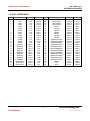
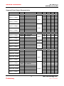
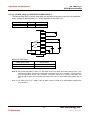
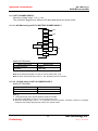
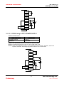
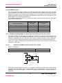
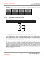
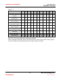
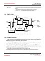
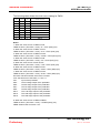
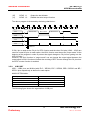
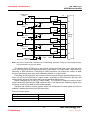
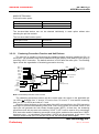
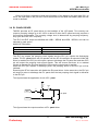
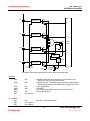
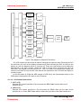
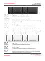
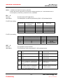
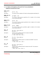
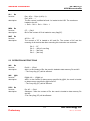
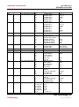
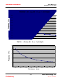
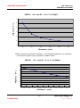
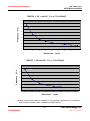
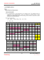
1
DS-TM8722_E 4-Bit Microcontroller Advance Information TM8722 4-Bit Microcontroller with LCD Driver User Manual tenx reserves the right to change or discontinue the manual and online documentation to this product herein to improve reliability, function or design without further notice. tenx does not assume any liability arising out of the application or use of any product or circuit described herein; neither does it convey any license under its patent rights nor the rights of others. tenx products are not designed, intended, or authorized for use in life support appliances, devices, or systems. If Buyer purchases or uses tenx products for any such unintended or unauthorized application, Buyer shall indemnify and hold tenx and its officers, employees, subsidiaries, affiliates and distributors harmless against all claims, cost, damages, and expenses, and reasonable attorney fees arising out of, directly or indirectly, any claim of personal injury or death associated with such unintended or unauthorized use even if such claim alleges that tenx was negligent regarding the design or manufacture of the part. 1 Preliminary tenx technology inc. Rev 1.4, 2011/12/30 DS-TM8722_E 4-Bit Microcontroller Advance Information AMENDMENT HISTORY Version Date Description V1.0 Oct, 2003 New release. V1.1 Nov, 2003 Modify page 5, 8, 14, 16~18, 21, 66, 68, 70, 72, 75~81, 106, 120. V1.2 May, 2009 Add experiment data. V1.3 Nov, 2009 Add circuit diagram description for LCD 1.5V 1/3 Bias. V1.4 Dec, 2011 Add Ordering Information table 2 Preliminary tenx technology inc. Rev 1.4, 2011/12/30 DS-TM8722_E 4-Bit Microcontroller Advance Information CONTENTS AMENDMENT HISTORY..................................................................................................... 2 Chapter 1 General Description ....................................................................................... 6 1-1. 1-2. 1-3. 1-4. 1-5. 1-6. 1-7. 1-1. GENERAL DESCRIPTION .................................................................... 6 FEATURES ........................................................................................... 6 BLOCK DIAGRAM................................................................................. 7 PAD DIAGRAM ..................................................................................... 8 PAD COORDINATE .............................................................................. 9 PIN DESCRIPTION ............................................................................. 10 CHARACTERISTICS........................................................................... 11 TYPICAL APPLICATION CIRCUIT ..................................................... 14 Chapter 2 TM8722 Internal System Architecture......................................................... 15 2-1. Power Supply ...................................................................................... 15 2-2. SYSTEM CLOCK ................................................................................ 22 2-3. PROGRAM COUNTER (PC) ............................................................... 29 2-4. PROGRAM/TABLE MEMORY ............................................................ 31 2-5. INDEX ADDRESS REGISTER (@HL) ................................................ 33 2-6. STACK REGISTER (STACK) .............................................................. 33 2-7. DATA MEMORY (RAM) ...................................................................... 34 2-8. WORKING REGISTER (WR) .............................................................. 35 2-9. ACCUMULATOR (AC) ........................................................................ 35 2-10. ALU (Arithmetic and Logic Unit) .......................................................... 35 2-11. BINARY CONVERT TO DECIMAL (BCD) ........................................... 36 2-12. TIMER 1 (TMR1) ................................................................................. 37 2-13. TIMER 2 (TMR2) ................................................................................. 40 2-14. STATUS REGISTER (STS)................................................................. 44 2-15. CONTROL REGISTER (CTL) ............................................................. 49 2-16 HALT FUNCTION ................................................................................ 53 2-17 STOP FUNCTION (STOP) .................................................................. 53 2-1 BACK UP FUNCTION .................................................................................. 55 Chapter 3 Control Function .......................................................................................... 57 3-1 NTERRUPT FUNCTION .............................................................................. 57 3-2 RESET FUNCTION ...................................................................................... 61 3-2 CLOCK GENERATOR ................................................................................. 65 3-4 BUZZER OUTPUT PINS .............................................................................. 68 3-5 INPUT / OUTPUT PORTS............................................................................ 70 3-6 EL PANEL DRIVER ...................................................................................... 77 3-7 EXTERNAL INT PIN ..................................................................................... 79 3-8 Resistor to Frequency Converter (RFC) ....................................................... 80 3-9 Key-Matrix Scanning Function...................................................................... 85 Chapter 4 LCD/LED DRIVER OUTPUT.......................................................................... 89 3 Preliminary tenx technology inc. Rev 1.4, 2011/12/30 DS-TM8722_E 4-Bit Microcontroller Advance Information 4-1 LCD DRIVER OUTPUT ................................................................................ 89 4-2 LED DRIVER OUTPUT ................................................................................ 97 Chapter 5 Detail Explanation of TM8722 Instructions .............................................. 110 5-1 INPUT / OUTPUT INSTRUCTIONS ........................................................... 111 5-2 ACCUMULATOR MANIPULATION INSTRUCTIONS AND MEMORY MANIPULATION INSTRUCTIONS .................................................... 116 5-3 OPERATION INSTRUCTIONS .................................................................. 117 5-4 LOAD/STORE INSTRUCTIONS ................................................................ 124 5-5 CPU CONTROL INSTRUCTIONS ............................................................. 126 5-6 INDEX ADDRESS INSTRUCTIONS .......................................................... 129 5-7 DECIMAL ARITHMETIC INSTRUCTIONS ................................................. 130 5-8 JUMP INSTRUCTIONS .............................................................................. 131 5-9 MISCELLANEOUS INSTRUCTIONS ......................................................... 132 ORDERING INFORMATION ........................................................................................... 138 Appendix A TM8722 Instruction Table ....................................................................... 139 Appendix B TM87 series Application Note ................................................................ 145 1. AP-TM87XX_11EV10 ................................................................................. 145 How to keep the content of data RAM for the duration of the Reset ..... 145 2. AP-TM87XX_13EV10 ................................................................................. 146 How to minimize the power noise in the system design which will cause MCU malfunction .................................................................................. 146 3. AP-SZ061_02EV10 .................................................................................... 147 Use I/O port to implement the Key Control function Control.................. 147 I. Basic features ....................................................................... 147 II. The definition of the keys ...................................................... 147 III. Talbe ROM addressing ......................................................... 147 IV. RAM addressing ................................................................... 148 V. A few applications tips ........................................................... 148 VI. EL light control explanation ................................................... 148 VII. Flow Chart............................................................................. 150 4. AP-SZ062_01EV10 .................................................................................... 152 Introduction to all the clock modes in the TM87 series.......................... 152 I. Fast only mode ..................................................................... 152 II. Slow only mode..................................................................... 158 III. Dual Clock mode................................................................... 165 5. AP-SZ077_01EV10 .................................................................................... 166 How to make bonding option for TM87/89 series MCU? ....................... 166 I. Introduction:........................................................................ 166 II. Use I/O for bonding option ................................................... 166 III. Use the INT pin for bonding option ....................................... 167 IV. Miscellaneous notes ............................................................. 168 V. Application Circuit ................................................................. 169 6. AP-SZ081_01EV10 .................................................................................... 170 TM87xx series KEYSCAN with shared segment ................................... 170 4 Preliminary tenx technology inc. Rev 1.4, 2011/12/30 DS-TM8722_E 4-Bit Microcontroller Advance Information I. Summary............................................................................... 170 II. Description ............................................................................ 170 III. TM87 series chips’ hardware scanning signals ..................... 171 IV. The Entire KEYSCAN Process ............................................. 172 V. The KEYSCAN program listing ............................................. 174 VI. Miscellaneous notes ............................................................. 176 VII. Application Circuit Diagram ................................................... 177 7. AP-SZ082_01EV11 .................................................................................... 178 TM87xx series Halt Release and Stop Release .................................... 178 8. AP-TM87XX_02EV12 ................................................................................. 186 The solution to “How to avoid the Crystal oscillator being stopped by external interference when BCF flag is cleared to 0?” as TM87 series products applying to 3V power supply and LCD 1/3 bias. ..................... 186 9. AP-TM87XX_10EV12 ................................................................................. 188 The application of large sized LCD panel.............................................. 188 10. AP-TM87XX_12EV10 ................................................................................. 189 The differences between TM8797 Demo Board/TM8795 and Mask type MCU in CX/SEG24 pin function ............................................................ 189 11. AP-TM8722_01EV10 ................................................................................. 190 TM8722 Electrical Characteristics ......................................................... 190 5 Preliminary tenx technology inc. Rev 1.4, 2011/12/30 DS-TM8722_E 4-Bit Microcontroller Advance Information Chapter 1 General Description 1-1. GENERAL DESCRIPTION The TM8722 is an embedded high-performance 4-bit micro-controller with LCD/LED driver on a chip. It contains all the necessary functions for a micro-controller, such as 4-bit parallel processing ALU, ROM, RAM, I/O ports, timer, clock generator, dual clock operation, Resistance to Frequency Converter(RFC), EL panel driver, LCD driver, look-up table, watchdog timer and key matrix scanning circuitry etc. on a single chip. 1-2. FEATURES 1. Low power dissipation. 2. Powerful instruction set (143 instructions). Binary addition subtraction, BCD conversion, logical operation in direct and index addressing mode. Single-bit manipulation (set, reset, decision for branch). Various conditional branches. 16 working registers and manipulation. Look-up Table. LCD driver with data transfer. 3. 4. Memory capacity. ROM capacity 2048 x 16 bits. RAM capacity 128 x 4 bits. LCD/LED driver output. 5 common outputs and 35 segment outputs (drive up to 175 LCD/LED segments). 1/2 Duty, 1/3 Duty, 1/4 Duty or 1/5 Duty for both LCD/LED drivers selectable in mask option. 1/2 Bias or 1/3 Bias for LCD driver selectable in mask option. Single instruction to turn off all segments. All segment outputs can be defined as CMOS or P_open drain output type in mask option. 5. Input/output ports. Port IOA 4 pins (with internal pull-low), muxed with SEG24~27. Port IOB 4 pins (with internal pull-low), muxed with SEG28~31. Port IOC 4 pins (with internal pull-low/ low-level-hold), muxed with SEG32~35. IOC port with built-in input signal chattering prevention circuitry. 6. 8 level subroutine nesting. 7. Interrupt function. 8. External factors 3 (INT pin, Port IOC & KI input). Internal factors 4 (Pre-Divider, Timer1, Timer2 & RFC). Built-in EL panel driver. 6 Preliminary tenx technology inc. Rev 1.4, 2011/12/30 DS-TM8722_E 4-Bit Microcontroller Advance Information ELC, ELP (Muxed with SEG28, SEG29). 9. Built-in Alarm, clock or single tone melody generator. BZB, BZ (Muxed with SEG30, SEG31). 10. Built-in R to F Converter circuit. CX, RR, RT, RH (Muxed with SEG24~SEG27). 11. Built-in key matrix scanning function. K1~K16 (Shared with SEG1~SEG16). KI1~KI4 (Muxed with SEG32~SEG35). 12. Two 6-bit programmable timers with programmable clock source. 13. Watch dog timer. 14. Built-in Voltage doubler, halver, tripler charge pump circuit. 15. Dual clock operation Slow clock oscillation can be defined as X’tal or external RC type oscillator in mask option. Fast clock oscillation can be defined as internal R or external R type oscillator in mask option. 16. HALT function. 17. STOP function. 1-3. BLOCK DIAGRAM B1-4 ELC,ELP BZ,BZB A1-4 CX RR,RT,RH C1-4 KI1~4 B-PORT EL DRIVER ALARM A-PORT RFC C-PORT KEY-IN SEG1-35 K1~K16 COM1-5 VDD1-3 LCD DRIVER SEGMENT PLA 4 BITS DATA BUS FREQUENCY GENERATOR INDEX ROM 256(16-N) X 8 BITS ALU DATA RAM 128 X 4 BITS PRE-DIVIDER 6 BITS PRESET TIMER 1 & 2 8 LEVELS STACK INSTRUCTION DECODER OSCILLATOR CONTROL CIRCUIT 11 BITS PROGRAM COUNTER MASK ROM 128N X 16 BITS CUP1,2 XTIN,OUT RESET N:1->16 INT 7 Preliminary tenx technology inc. Rev 1.4, 2011/12/30 DS-TM8722_E 4-Bit Microcontroller Advance Information 1-4. PAD DIAGRAM The chip substrate should be connected to GND. 52 40 1 Die size :1680um x 1680um (ROM) 14 27 8 Preliminary tenx technology inc. Rev 1.4, 2011/12/30 DS-TM8722_E 4-Bit Microcontroller Advance Information 1-5. PAD COORDINATE No 1 2 3 4 5 6 7 8 9 10 11 12 13 14 15 16 17 18 19 20 21 22 23 24 25 26 Name BAK XIN XOUT GND VDD1 VDD2 VDD3 CUP1 CUP2 COM1 COM2 COM3 COM4 COM5 SEG1/K1 SEG2/K2 SEG3/K3 SEG4/K4 SEG5/K5 SEG6/K6 SEG7/K7 SEG8/K8 SEG9/K9 SEG10/K10 SEG11/K11 SEG12/K12 X 77.5 77.5 77.5 77.5 77.5 77.5 77.5 77.5 77.5 77.5 77.5 77.5 77.5 77.5 207.5 322.5 437.5 552.5 667.5 782.5 897.5 1012.5 1127.5 1242.5 1357.5 1472.5 Y 1602.5 1472.5 1357.5 1242.5 1127.5 1012.5 897.5 782.5 667.5 552.5 437.5 322.5 207.5 77.5 77.5 77.5 77.5 77.5 77.5 77.5 77.5 77.5 77.5 77.5 77.5 77.5 No 27 28 29 30 31 32 33 34 35 36 37 38 39 40 41 42 43 44 45 46 47 48 49 50 51 52 9 Preliminary Name SEG13/K13 SEG14/K14 SEG15/K15 SEG16/K16 SEG17 SEG18 SEG19 SEG20 SEG21 SEG22 SEG23 SEG24/IOA1/CX SEG25/IOA2/RR SEG26/IOA3/RT SEG27/IOA4/RH SEG28/IOB1/ELC SEG29/IOB2/ELP SEG30/IOB3/BZB SEG31/IOB4/BZ SEG32/IOC1/KI1 SEG33/IOC2/KI2 SEG34/IOC3/KI3 SEG35/IOC4/KI4 RESET INT TEST X 1602.5 1602.5 1602.5 1602.5 1602.5 1602.5 1602.5 1602.5 1602.5 1602.5 1602.5 1602.5 1602.5 1602.5 1472.5 1357.5 1242.5 1127.5 1012.5 897.5 782.5 667.5 552.5 437.5 322.5 207.5 Y 77.5 207.5 322.5 437.5 552.5 667.5 782.5 897.5 1012.5 1127.5 1242.5 1357.5 1472.5 1602.5 1602.5 1602.5 1602.5 1602.5 1602.5 1602.5 1602.5 1602.5 1602.5 1602.5 1602.5 1602.5 tenx technology inc. Rev 1.4, 2011/12/30 DS-TM8722_E 4-Bit Microcontroller Advance Information 1-6. PIN DESCRIPTION Name I/O Description BAK P VDD1,2,3 P RESET INT I I TESTA CUP1,2 O XIN XOUT I O COM1~5 SEG1-35 IOA1-4 IOB1-4 IOC1-4 CX RR/RT/RH ELC/ELP BZB/BZ O O I/O I/O I/O I O O O Positive Back-up voltage. In Li power Mode, connect a 0.1u capacitor to GND. LCD supply voltage, and positive supply voltage. . In Ag Mode, it will connect a positive power to VDD1. . In Li or ExtV power mode, it will connect a positive power to VDD2. Input pin for external reset request signal. Built-in internal pull-down resistor. Input pin for external INT request signal. . It can be trigger by Falling edge or rising edge and is defined in mask option. . Internal pull-down or pull-up resistor is defined in mask option. Test signal input pin. Switching pins for supplying the LCD driving voltage to the VDD1, 2, 3 pins. . Connect the CUP1 and CUP2 pins with non-polarized electrolytic capacitor when chip operates in 1/2 or 1/3 bias mode. . In no BIAS mode application, leave these pins open. Input /Output pins for slow clock oscillator. . 32KHz Crystal oscillator. . In FAST mode, connect an external resistor to form a RC oscillator (mask option). . In SLOW mode, connect an external resistor to form a RC oscillator (mask option). Output pins for driving the common pins for the LCD or LED panel. Output pins for driving the LCD or the LED panel segment. Input / Output port A. (Muxed with SEG24~SEG27) Input / Output port B. (Muxed with SEG28~SEG31) Input / Output port C. (Muxed with SEG32~SEG35) RFC application with 1 input pin and 3 output pins. (Muxed with SEG24~SEG27) K1~K16 KI1~4 GND O I P Output port for the EL panel driver. (Muxed with SEG28,SEG29) Output port for alarm, clock or the single melody tone generator. (Muxed with SEG30~SEG31) Output port for the key matrix scanning.(Shared with SEG1~SEG16) Input port for the key matrix scanning.(Muxed with SEG32~SEG35) Negative supply voltage. 10 Preliminary tenx technology inc. Rev 1.4, 2011/12/30 DS-TM8722_E 4-Bit Microcontroller Advance Information 1-7. CHARACTERISTICS ABSOLOUTE MAXIMUM RATINGS GND= 0V Name Symbol VDD1 Maximum Supply Voltage VDD2 VDD3 Maximum Input Voltage Vin Maximum output Voltage Vout1 Vout2 Maximum Operating Temperature Topg Maximum Storage Temperature Tstg Range -0.3 to 5.5 -0.3 to 5.5 -0.3 to 8.5 -0.3 to VDD1/2+0.3 -0.3 to VDD1/2+0.3 -0.3 to VDD3+0.3 -20 to +70 -25 to +125 Unit V V V V V V ℃ ℃ POWER CONSUMPTION at Ta=-20℃ to 70℃,GND= 0V Name HALT mode STOP mode Sym. Condition IHALT Only the 32.768KHz Crystal oscillator is 1 operating without loading. Ag mode, VDD1=1.5V, BCF = 0 IHALT Only 32.768KHz Crystal oscillator is 2 operating, without loading. Li mode, VDD2=3.0V, BCF = 0 ISTOP Min. Typ. 2 Max. 5 Unit uA 2 5 uA 1 uA Note : When using RC oscillator, the current consumption will depend on the frequency of oscillation. ALLOWABLE OPERATING CONDITIONS at Ta=-20℃ to 70℃,GND= 0V Name Supply Voltage Symb. VDD1 VDD2 VDD3 Condition Oscillator Start-Up Voltage VDDB Crystal Mode Oscillator Sustain Voltage VDDB Crystal Mode Supply Voltage Supply Voltage Input “H” Voltage Input “L” Voltage Input “H” Voltage Input “L” Voltage Input “H” Voltage Input “L” Voltage Input “H” Voltage Input “L” Voltage Input “H” Voltage VDD1 VDD2 Vih1 Vil1 Vih2 Vil2 Vih3 Vil3 Vih4 Vil4 Vih5 Ag Mode EXT-V, Li Mode Ag Battery Mode Li Battery Mode OSCIN in Ag Battery Mode OSCIN in Li Battery Mode CFIN in Li Battery or EXT-V 11 Preliminary Min. 1.2 2.4 2.4 Max. 5.25 5.25 8.0 1.3 1.2 1.2 2.4 VDD1-0.7 -0.7 VDD2-0.7 -0.7 0.8xVDD1 0 0.8xVDD2 0 0.8xVDD2 Unit V V V V 1.65 5.25 VDD1+0.7 0.7 VDD2+0.7 0.7 VDD1 0.2xVDD1 VDD2 0.2xVDD2 VDD2 V V V V V V V V V V V V tenx technology inc. Rev 1.4, 2011/12/30 DS-TM8722_E 4-Bit Microcontroller Advance Information Input “L” Voltage Input “H” Voltage Input “L” Voltage Vil5 Vih6 Vil6 Fopg1 Fopg2 Operating Freq Mode 0 0.8xVDDO 0 32 10 RC Mode Crystal Mode RC Mode 0.2xVDD2 VDDO 0.2xVDDO 1000 V V V KHZ KHZ INTERNAL RC FREQUENCY RANGE Option Mode 250KHz 500KHz BAK 1.5V 3.0V 1.5V 3.0V Min. 200KHz 200KHz 450KHz 400KHz Typ. 300KHz 250KHz 600KHz 500KHz Max. 400KHz 300KHz 750KHz 600KHz ELECTRICAL CHARACTERISTICS at#1:VDD1=1.2V(Ag); at#2:VDD2=2.4V(Li): at#3:VDD2=4V(Ext-V); Input Resistance Name “L” Level Hold Tr(IOC) IOA/B/C Pull-Down Tr INT Pull-up Tr INT Pull-Down Tr RES Pull-Down R Symb. Rllh1 Rllh2 Rllh3 Rmad1 Rmad2 Rmad3 Rintu1 Rintu2 Rintu3 Rintd1 Rintd2 Rintd3 Rres1 Rres2 Rres3 Condition Vi=0.2VDD1,#1 Vi=0.2VDD2,#2 Vi=0.2VDD2,#3 Vi=VDD1,#1 Vi=VDD2,#2 Vi=VDD2,#3 Vi=VDD1,#1 Vi=VDD2,#2 Vi=VDD2,#3 Vi=GND,#1 Vi=GND,#2 Vi=GND,#3 Vi=GND or VDD1,#1 Vi=GND or VDD2,#2 Vi=GND or VDD2,#3 Min. 10 10 5 200 200 100 200 200 100 200 200 100 10 10 10 Typ. 40 40 20 500 500 250 500 500 250 500 500 250 40 40 40 Max. 100 100 50 1000 1000 500 1000 1000 500 1000 1000 500 100 100 100 Unit Kohm Kohm Kohm Kohm Kohm Kohm Kohm Kohm Kohm Kohm Kohm Kohm Kohm Kohm Kohm DC Output Characteristics Name Output ”H” Voltage Output ”L” Voltage Symb. Voh1c Voh2c Voh3c Vol1c Vol2c Vol3c Condition Ioh=-200uA,#1 Ioh=-1mA,#2 Ioh=-3mA,#3 Iol=400uA,#1 Iol=2mA,#2 Iol=6mA,#3 12 Preliminary Port SEG1~35 Min. 0.8 1.5 2.5 0.2 0.3 0.5 Typ. 0.9 1.8 3.0 0.3 0.6 1.0 Max. 1.0 2.1 3.5 0.4 0.9 1.5 Unit V V V V V V tenx technology inc. Rev 1.4, 2011/12/30 DS-TM8722_E 4-Bit Microcontroller Advance Information Segment Driver Output Characteristics Name Output ”H” Voltage Output ”L” Voltage Output ”H” Voltage Output ”L” Voltage Output ”H” Voltage Output ”L” Voltage Output ”H” Voltage Output ”M” Voltage Output ”L” Voltage Output ”H” Voltage Output ”M1” Voltage Output ”M2” Voltage Output ”L” Voltage Output ”H” Voltage Output ”M1” Voltage Output ”M2” Voltage Output ”L” Voltage Symb. Condition For Static Display Mode Voh1d Ioh=-1uA,#1 Voh2d Ioh=-1uA,#2 Voh3d Ioh=-1uA,#3 SEG-n Vol1d Iol=1uA,#1 Vol2d Iol=1uA,#2 Vol3d Iol=1uA,#3 Voh1e Ioh=-10uA,#1 Voh2e Ioh=-10uA,#2 Voh3e Ioh=-10uA,#3 COM-n Vol1e Iol=10uA,#1 Vol2e Vol3e Voh12f Voh3f Vol12f Vol3f Voh12g Voh3g Vom12g Vom3g Vol12g Vol3g Voh12i Voh3i Vom12i Vom13i Vom22i Vom23i Vol12i Vol3i Voh12j Voh3j Vom12j Vom13j Vom22j Vom23j Vol12j Vol3j Iol=10uA,#2 Iol=10uA,#3 1/2 Bias Display Mode Ioh=-1uA,#1,#2 Ioh=-1uA,#3 SEG-n Iol=1uA,#1,#2 Iol=1uA,#3 Ioh=-10uA,#1,#2 COM-n Ioh=-10uA,#3 Iol/h=+/-10uA,#1,#2 Iol/h=+/-10uA,#3 COM-n Iol=10uA,#1,#2 Iol=10uA,#3 1/3 Bias display Mode Ioh=-1uA,#1,#2 Ioh=-1uA,#3 Iol/h=+/-10uA,#1,#2 Iol/h=+/-10uA,#3 Iol/h=+/-10uA,#1,#2 SEG-n Iol/h=+/-10uA,#3 Iol=1uA,#1,#2 Iol=1uA,#3 Ioh=-10uA,#1,#2 Ioh=-10uA,#3 Iol/h=+/-10uA,#1,#2 Iol/h=+/-10uA,#3 Iol/h=+/-10uA,#1,#2 COM-n Iol/h=+/-10uA,#3 Iol=10uA,#1,#2 Iol=10uA,#3 13 Preliminary Min. Typ. Max. 1.0 2.2 3.8 0.2 0.2 0.2 1.0 2.2 3.8 0.2 0.2 0.2 2.2 3.8 0.2 0.2 2.2 3.8 1.0 1.8 3.4 5.8 1.0 1.8 2.2 3.8 3.4 5.8 1.0 1.8 2.2 3.8 1.4 2.2 0.2 0.2 1.4 2.2 2.6 4.2 0.2 0.2 1.4 2.2 2.6 4.2 0.2 0.2 Unit. V V V V V V V V V V V V V V V V V V V V V V V V V V V V V V V V V V V V V V tenx technology inc. Rev 1.4, 2011/12/30 DS-TM8722_E 4-Bit Microcontroller Advance Information 1-1. TYPICAL APPLICATION CIRCUIT This application circuit is only an example, and can not be guaranteed to work. LCD Panel COM1~5, SEG1~23 15P CUP1 XIN 15P 0.1u 32.768KHz Crystal XOUT CUP2 VDD3 0.1u VDD2 RH VDD1 RT BAK RR CX 0.1u 0.1u 0.1u 3.0V GND TM8722 L 0.1u ELP EL Plant RESET External INT. I/O Port INT ELC IOA,IOB,IOC Choke Buzzer BZ(BZB) K1~16 KI1~KI 4 Key Scanning Key Matrix Li power mode, 1/3 Bias, 1/5 Duty 14 Preliminary tenx technology inc. Rev 1.4, 2011/12/30 DS-TM8722_E 4-Bit Microcontroller Advance Information Chapter 2 TM8722 Internal System Architecture 2-1. Power Supply TM8722 can operate using 3 types of supply voltage: Ag, Li, and EXTV, which can be selected in mask option. The power supply circuitry selected will also provide the necessary voltage level to drive the LCD panel with different biases. The connection diagrams for 1/2 bias,1/3 bias and no bias applications are shown below. 2-1-1. Ag BATTERY POWER SUPPLY Operating voltage range : 1.2V ~ 1.8V. The connection diagrams for different LCD bias applications are shown below: 2-1-1-1. NO LCD BIAS NEEDED using a Ag BATTERY POWER SUPPLY N.C. CUP2 N.C. CUP1 GND BAK VDD1 VDD2 VDD3 + Application circuit TM8722 MASK OPTION table : Mask Option name POWER SOURCE LCD BIAS Selected item (3) 1.5V BATTERY (3) NO BIAS Note 1: The input/output ports operate between GND and VDD1. Note 2: The backup flag (BCF) is set to 1 in the initial reset cycle. When as the backup flag is set to 1, the driving capability of the oscillator circuit increases, it improves the oscillation conditions but the operating current also increases. Therefore, unless it is required, otherwise, the backup flag must be reset to 0 after the initial reset cycle. For the the backup flag, please refer to 3-5. 15 Preliminary tenx technology inc. Rev 1.4, 2011/12/30 DS-TM8722_E 4-Bit Microcontroller Advance Information 2-1-1-2. 1/2 BIAS & STATIC using a AG BATTERY POWER SUPPLY CUP1 0.1U CUP2 VDD3 VDD2 VDD1 0.1U Internal logic 1.5V BAK GND MASK OPTION table : Mask Option name POWER SOURCE LCD BIAS Selected item (3) 1.5V BATTERY (2) 1/2 BIAS Note 1: The input/output ports operate between GND and VDD1. Note 2: The backup flag (BCF) is set to 1 in the initial reset cycle. When the backup flag is set to 1, the driving power of the oscillator circuit increases, it improves the oscillation conditions but the operating current also increases. Therefore, unless it is required, otherwise, the backup flag must be reset to 0 after the initial reset cycle. For the backup flag, please refer to 3-5. 2-1-1-3. 1/3 BIAS using a AG BATTERY POWER SUPPLY CUP1 0.1U CUP2 VDD3 VDD2 VDD1 Internal logic BAK 0.1U 0.1U 1.5V GND 16 Preliminary tenx technology inc. Rev 1.4, 2011/12/30 DS-TM8722_E 4-Bit Microcontroller Advance Information MASK OPTION table : Mask Option name POWER SOURCE LCD BIAS Selected item (3) 1.5V BATTERY (1) 1/3 BIAS Note 1: The input/output ports operate between GND and VDD1. Note 2: The backup flag (BCF) is set to 1 in the initial reset cycle. When the backup flag is set to 1, the driving power of the oscillator circuit increases, it improves the oscillation conditions but the operating current also increases. Therefore, unless it is required, otherwise, the backup flag must be reset to 0 after the initial reset cycle. For the backup flag, please refer to 3-5. 2-1-2. LI BATTERY POWER SUPPLY Operating voltage range : 2.4V ~ 3.6V. The connection diagrams for different LCD bias applications are shown below : 2-1-2-1. NO BIAS using a LI BATTERY POWER SUPPLY N.C. CUP2 N.C. CUP1 GND BAK VDD1 VDD2 VDD3 + Application circuit TM8722 MASK OPTION table : Mask Option name POWER SOURCE LCD BIAS Selected item (2) 3V BATTERY OR HIGHER (3) NO BIAS Note 1: The input/output ports operate between GND and VDD2. 17 Preliminary tenx technology inc. Rev 1.4, 2011/12/30 DS-TM8722_E 4-Bit Microcontroller Advance Information 2-1-2-2. 1/2 BIAS using a LI BATTERY POWER SUPPLY The backup flag (BCF) must be reset after the operation of the halver circuit is fully stabilized and a voltage of approximately 1/2 * VDD2 appears on the VDD1 pin. Backup flag(BCF) BCF=0 BCF=1 SW1 ON OFF SW2 OFF ON CUP1 0.1U CUP2 VDD3 VDD2 SW2 VDD1 3.0V SW1 BAK Internal logic 0.1U 0.1U GND MASK OPTION table : Mask Option name POWER SOURCE LCD BIAS Selected item (2) 3V BATTERY OR HIGHER (2) 1/2 BIAS Note 1: The input/output ports operate between GND and VDD2. Note 2: The backup flag (BCF) is set to 1 in the initial reset cycle. When the backup flag is set to 1, the internal logic signal operated on VDD2 and the driving power of the oscillator circuit increases and the operating current also increases. Therefore, unless it is required, otherwise, the backup flag must be reset to 0 after the initial reset cycle. For the backup flag, please refer to 3-5. Note 3: The VDD1 level (≈1/2 * VDD2) in the off-state of SW1 is used as an intermediate voltage level for the LCD driver. 18 Preliminary tenx technology inc. Rev 1.4, 2011/12/30 DS-TM8722_E 4-Bit Microcontroller Advance Information 2-1-2-3. 1/3 BIAS using a LI BATTERY POWER SUPPLY The backup flag (BCF) must be reset after the operation of the halver circuit is fully stabilized and a voltage of approximately 1/2 * VDD2 appears on the VDD1 pin. Backup flag(BCF) BCF=0 BCF=1 SW1 ON OFF SW2 OFF ON CUP1 0.1U CUP2 VDD3 0.1U SW2 VDD2 VDD1 SW1 3.0V 0.1U BAK Internal logic 0.1U GND MASK OPTION table : Mask Option name POWER SOURCE LCD BIAS Selected item (2) 3V BATTERY OR HIGHER (1) 1/3 BIAS Note 1: The input/output ports operate between GND and VDD2. Note 2: The backup flag (BCF) is set to 1 in the initial reset cycle. When the backup flag is set to 1, the internal logic signal operated on VDD2 and the driving power of the oscillator circuit increases and the operating current also increases. Therefore, unless it is required, otherwise, the backup flag must be reset to 0 after the initial reset cycle. For the backup flag, please refer to 3-5. Note 3: The VDD1 level (≈1/2 * VDD) in the off-state of SW1 is used as an intermediate voltage level for LCD driver. 19 Preliminary tenx technology inc. Rev 1.4, 2011/12/30 DS-TM8722_E 4-Bit Microcontroller Advance Information 2-1-3. EXTV POWER SUPPLY Operating voltage range : 3.6V ~ 5.4V. The connection diagrams for different LCD bias applications are shown below : 2-1-3-1. NO BIAS using an EXT-V BATTERY POWER SUPPLY CUP1 NC CUP2 NC VDD3 VDD2 Internal logic VDD1 EXTV BAK GND MASK OPTION table : Mask Option name POWER SOURCE LCD BIAS Selected item (1) EXT-V (3) NO BIAS Note 1: The input/output ports operate between GND and VDD2. Note 2: the backup flag (BCF) is reset to 0 in the initial reset cycle. Note 3: When the backup flag is set to 1, the operating current increases. 2-1-3-2. 1/2 BIAS using an EXT-V POWER SUPPLY MASK OPTION table : Mask Option name POWER SOURCE LCD BIAS Selected item (1) EXT-V (2) 1/2 BIAS Note: 1. The input/output ports operate between GND and VDD2. 2. the backup flag (BCF) is reset to 0 in the initial reset cycle. 3. When the backup flag is set to 1, the operating current increases. Therefore, unless it is required, otherwise, the backup flag must be reset to 0 in normal mode. 20 Preliminary tenx technology inc. Rev 1.4, 2011/12/30 DS-TM8722_E 4-Bit Microcontroller Advance Information CUP1 0.1U CUP2 VDD3 VDD2 EXTV VDD1 0.1U BAK Internal logic GND 2-1-3-3. 1/3 BIAS using an EXT-V POWER SUPPLY MASK OPTION table : Mask Option name POWER SOURCE LCD BIAS Selected item (1) EXT-V (1) 1/3 BIAS Note 1: The input/output ports operate between GND and VDD2. Note 2: the backup flag (BCF) is reset to 0 in the initial reset cycle. Note 3: When the backup flag is set to 1, the operating current increases. Therefore, unless it is required, otherwise, the backup flag must be reset to 0 in normal mode. CUP1 0.1U CUP2 VDD3 VDD2 0.1U VDD1 EXT-V BAK Internal logic 0.1U GND 21 Preliminary tenx technology inc. Rev 1.4, 2011/12/30 DS-TM8722_E 4-Bit Microcontroller Advance Information 2-2. SYSTEM CLOCK The clock oscillation circuitry consists of a XT clock (slow clock) oscillator and a CF clock (fast clock) oscillator. The output from this circuitry forms the clock source for the system clock generator (provides the necessary clock signals for the execution of instructions), the predivider (generates several clock signals with different frequencies to be used by the LCD driver),and for the frequency generator etc. The following table shows the clock sources of system clock generator and the pre-divider under different conditions. PH0(per-divider) XT clock CF clock XT clock XT clock XT clock XT clock Slow clock only option fast clock only option Initial state(dual clock option) Halt mode(dual clock option) Slow mode(dual clock option) Fast mode(dual clock option) BCLK(system clock) XT clock CF clock XT clock XT clock XT clock CF clock 2-2-1. CONNECTION DIAGRAM OF THE SLOW CLOCK OSCILLATOR (XT CLOCK) This clock oscillator provides the lower speed clock signals to the system clock generator, the pre-divider, the timer, the chattering prevention of the IO port and the LCD circuitry. This oscillator is disabled when the “fast clock only “option is selected in mask option, otherwise it is active all the time after the initial reset cycle. In stop mode, this oscillator will be stopped. There are 2 types of oscillators that can be used as the slow clock oscillator, which can be selected in mask option : 2-2-1-1. External 32.768KHz Crystal oscillator (XT CLOCK) MASK OPTION table : Mask Option name SLOW CLOCK TYPE FOR SLOW ONLY OR DUAL Selected item (1) X’tal XOUT 15p f XIN 15p f 32768H z Crystal (1) X'tal When the backup flag (BCF) is set to 1, the oscillator operates in a state with a higher driving capability and the start-up time of the oscillator can be reduced as a result. However it increases the power consumption. Therefore, the backup flag should be reset unless required otherwise. 22 Preliminary tenx technology inc. Rev 1.4, 2011/12/30 DS-TM8722_E 4-Bit Microcontroller Advance Information The following table shows the power consumption of Crystal oscillator under different conditions : BCF=1 BCF=0 Initial reset After reset 2-2-1-2. Ag power option Increase Normal Increase Increase Li power option Increase Normal Increase Increase EXT-V option Increase Increase Increase Increase External RC oscillator (XT CLOCK) MASK OPTION table : Mask Option name SLOW CLOCK TYPE FOR SLOW ONLY OR DUAL Selected item (2) RC XOUT R XIN C (2) RC 2-2-2. CONNECTION DIAGRAM OF THE FAST CLOCK OSCILLATOR (CF CLOCK) The CF clock consists of 3 types of oscillators (selectable in mask option) which provides a faster clock sources to the system. In single clock operation (fast only), this oscillator provides the clock signals to the system clock generator, the pre-divider, the timer, the I/O port chattering prevention clock and the LCD circuitry. In dual clock operation, CF clock provides the clock signals to the system clock generator only. When the dual clock option is selected in mask option, this oscillator is inactive most of the time except when the FAST instruction is executed. After the FAST instruction is executed, the clock source (BCLK) of the system clock generator will be switched to CF clock but the clock source for other functions will still come in from the XT clock. The Halt mode, the stop mode and the execution of the SLOW instruction will stop this oscillator and the system clock (BCLK) will be switched to the XT clock. There are 3 types of oscillators that can be used as the fast clock oscillator, which can be selected in mask option : 23 Preliminary tenx technology inc. Rev 1.4, 2011/12/30 DS-TM8722_E 4-Bit Microcontroller Advance Information 2-2-2-1. RC OSCILLATOR WITH EXTERNAL RESISTOR (CF CLOCK) This type of oscillator can only be used in the “FAST only” option, however, this oscillator can not be used as the fast clock source in dual clock mode. When this oscillator is selected in mask option, the RC oscillator with internal RC will be disabled. MASK OPTION table : Mask Option name CLOCK SOURCE Selected item (2) FAST ONLY & USE EXTERNAL RESISTOR MASK OPTION table : Mask Option name Selected item FAST CLOCK OSC TYPE FOR FAST ONLY OR DUAL (1) or (2), don’t care XTOUT R XTIN External Resistor 2-2-2-2. RC OSCILLATOR WITH INTERNAL RESISTOR (CF CLOCK) Two frequencies can be selected in this type of oscillator: 250KHz and 500KHz. When the oscillator is used, CFOUT and CFIN pins should be left open. This type of oscillator can be used both in the “FAST only” and the “DUAL clock” options. MASK OPTION table : Mask Option name CLOCK SOURCE Selected item (1) FAST ONLY & USE EXTERNAL RESISTOR or (4) DUAL For 250KHz output frequency : Mask Option name Selected item FAST CLOCK OSC TYPE FOR FAST ONLY OR DUAL (1) INTERNAL RESISTOR FOR 250KHz For 500KHz output frequency : Mask Option name Selected item FAST CLOCK OSC TYPE FOR FAST ONLY OR DUAL (2) INTERNAL RESISTOR FOR 500KHz 24 Preliminary tenx technology inc. Rev 1.4, 2011/12/30 DS-TM8722_E 4-Bit Microcontroller Advance Information XTOUT N.C. XTIN N.C. Internal RC FREQUENCY RANGE OF INTERNAL RC OSCILLATOR Option Mode 250KHz 500KHz BAK 1.5V 3.0V 1.5V 3.0V Min. 200KHz 200KHz 450KHz 400KHz Typ. 300KHz 250KHz 600KHz 500KHz Max. 400KHz 300KHz 750KHz 600KHz 2-2-3. COMBINATION OF THE CLOCK SOURCES (CLCOK SWITCH CIRCUIT) The clock switch circuit allows the selection of different clock inputs from XTOSC and CFOSC. There are three combinations of the clock sources that can be selected in mask option: 2-2-3-1 DUAL CLOCK MASK OPTION table : Mask Option name CLOCK SOURCE Selected item (4) DUAL The operation of the dual clock mode is shown in the following figure. When this mode is selected in mask option, the clock source (BCLK) of the system clock generator will switch between XT clock and CF clock according to the user’s program. When the HALT and STOP instructions are executed, the clock source (BCLK) will switch to the XT clock automatically. The XT clock provides the clock signals to the pre-divider, the timer, the I/O port chattering prevention and the LCD circuitry in this mode. 25 Preliminary tenx technology inc. Rev 1.4, 2011/12/30 DS-TM8722_E 4-Bit Microcontroller Advance Information Halt Halt mode XTOSC:active CFOSC:stop Halt HALT released Stop released Power-on reset Reset pin reset Watchdog timer reset Key reset Slow mode XTOSC:active CFOSC:stop Reset release Slow Fast Fast mode XTOSC: active CFOSC: active Stop Reset Reset state XTOSC:active CFOSC:stop Reset Stop mode XTOSC: stop CFOSC: stop The state diagram of the dual clock mode is shown in the above figure. After the execution of the FAST instruction, the system clock generator will hold for 12 CF clock cycles after the CF clock oscillator starts up and then BCLK will switch to the CF clock. It prevents the delivery of incorrect clock signals to the system clock in the start-up duration of the fast clock oscillator. CF clock XT clock FAST BCLK HOLD 12 CF CLOCKS This figure shows the System Clock Switches from Slow to Fast After executing SLOW instruction, the system clock generator will hold for 2 XT clock cycles and then BCLK will switch to the XT clock. 26 Preliminary tenx technology inc. Rev 1.4, 2011/12/30 DS-TM8722_E 4-Bit Microcontroller Advance Information CF clock Fast clock stops operating XT clock SLOW BCLK This figure shows the System Clock Switches from Fast to Slow 2-2-3-2 SINGLE CLOCK MASK OPTION table : For Fast clock oscillator only Mask Option name CLOCK SOURCE Selected item (1) FAST ONLY & USE INTERNAL RESISTOR or (2) FAST ONLY & USE EXTERNAL RESISTOR For slow clock oscillator only Mask Option name CLOCK SOURCE Selected item (3) SLOW ONLY The operation of the single clock option is shown in the following figure. Either XT or CF clock can be selected in mask option in this mode. The FAST and SLOW instructions will be treated as the NOP instruction in this mode. The backup flag (BCF) will be set to 1 automatically before the program enters the stop mode. It can ensure that the Crystal oscillator starts up in a favorable condition. Normal mode OSC:active Reset release Power -on reset Reset pin reset Watchdog timer reset Key reset Halt Halt released Stop Reset Reset mode OSC:active Halt mode OSC:active Stop Release Reset Stop mode OSC: stop This figure shows the State Diagram of Single Clock Option 27 Preliminary tenx technology inc. Rev 1.4, 2011/12/30 DS-TM8722_E 4-Bit Microcontroller Advance Information 2-2-4 PREDIVIDER The pre-divider is a 15-stage counter that receives the clock signals from the output of the clock switch circuitry (PH0). When PH0 changes from "H" level to "L" level, the content of this counter changes accordingly. The PH11 to PH15 of the pre-divider are reset to "0" when the PLC 100H instruction is executed or in the initial reset cycle. The pre-divider delivers the signals to the halver/tripler circuit, the LCD driver, the sound generator and the I/O port chattering prevention function. Frequency Generator XTOSC HEF3 BCLK Halt mode SLOW instruction FAST instruction Initial PLC 8H Interrupt T1 T2 T3 T4 Sclk Clock switch circuit Interrupt request IEF3 SCF7 R Q Fall edge detector System clock generator S HRF3 HALT release request flag MSC instruction Data bus 2 CFOSC Clock switch circuit To timer circuit PH0 PLC 100H initial R R R R R Single clock option Dual clock option PH5 PH3 PH1 PH2 PH4 PH7 PH6 PH9 PH8 PH11 PH10 PH13 PH12 PH15 PH14 To sound circuit Halver tribler circuit This figure shows the pre-divider and its peripherals The falling edge of PH14 will set the halt mode release request flag (HRF3) to 1, and if the pre-divider interrupt enable mode (IEF3) was also set in advance, the interrupt comes from predivider will be accepted; and if the halt release enable mode (HEF3) was also set in advance, then the halt release request signal will be delivered and the start condition flag 7 (SCF7) in status register 3 (STS3) will be set. The clock source of the pre-divider is PH0, there are 4 kinds of frequencies of PH0 that can be selected in mask option: MASK OPTION table : Mask Option name PH0 <-> BCLK FOR FAST ONLY PH0 <-> BCLK FOR FAST ONLY PH0 <-> BCLK FOR FAST ONLY PH0 <-> BCLK FOR FAST ONLY Selected item (1) PH0 = BCLK (2) PH0 = BCLK/4 (3) PH0 = BCLK/8 (4) PH0 = BCLK/16 28 Preliminary tenx technology inc. Rev 1.4, 2011/12/30 DS-TM8722_E 4-Bit Microcontroller Advance Information 2-2-5 SYSTEM CLOCK GENERATOR The system clock generator provides the necessary clock signals to control the execution of instructions. The FAST and SLOW instructions can also be used to switch the clock input of the system clock generator. The basic system clock is shown below: SCLK T1 T2 T3 T4 Machine Cycle Instruction Cycle 2-3. PROGRAM COUNTER (PC) The program counter is a 11-bit counter, which addresses the program memory (ROM) up to 2048 addresses. The program counter (PC) is normally incremented by one (+1) for every instruction execution. PC PC + 1 When executing JMP instruction, subroutine call instruction (CALL), interrupt service routine or when reset occurs, the program counter (PC) will be loaded with the corresponding address in table 2-1. PC corresponding address shown in Table 2- 1 When executing a jump instruction except JMP and CALL, the program counter (PC) will be loaded with the specified address in the operand of the instruction. PC current page (PC11) + specified address in the operand Return instruction (RTS) PC content of stack specified by the stack pointer Stack pointer stack pointer – 1 29 Preliminary tenx technology inc. Rev 1.4, 2011/12/30 DS-TM8722_E 4-Bit Microcontroller Advance Information Table 2- 1 Initial reset Interrupt 2 (INT pin) Interrupt 0 (input port C) Interrupt 1 (timer 1 interrupt) Interrupt 3 (pre-divider interrupt) Interrupt 4 (timer 2 interrupt) Interrupt 5 (Key Scanning interrupt) Interrupt 6 (RFC counter interrupt) Jump instruction Subroutine call PC10 PC9 0 0 PC8 0 PC7 0 PC6 0 PC5 0 PC4 0 PC3 0 PC2 0 PC1 0 PC0 0 0 0 0 0 0 0 1 0 0 0 0 0 0 0 0 0 0 1 0 1 0 0 0 0 0 0 0 0 1 1 0 0 0 0 0 0 0 0 0 1 1 1 0 0 0 0 0 0 0 1 0 0 0 0 0 0 0 0 0 0 1 0 0 1 0 0 0 0 0 0 0 1 0 1 0 0 0 P10 P10 P9 P9 P8 P8 P7 P7 P6 P6 P5 P5 P4 P4 P3 P3 P2 P2 P1 P1 P0 P0 P10 to P0 : the 11 Low-order bits of instruction operand. When executing a subroutine call or an interrupt service routine, the contents of the program counter (PC) will be automatically saved to the stack register (STACK). 30 Preliminary tenx technology inc. Rev 1.4, 2011/12/30 DS-TM8722_E 4-Bit Microcontroller Advance Information 2-4. PROGRAM/TABLE MEMORY The built-in mask ROM is organized into 2048 x 16 bits. 16 bits 000h 7FFh Both instruction ROM (PROM) and table ROM (TROM) share this memory space together. The partition formula for PROM and TROM is shown below: Instruction ROM memory space = (128 * N) words, Table ROM memory space = 256(16 - N) bytes (N = 1 ~ 16). Note : The data width of the table ROM is 8-bit The partition of memory space is defined in mask option, the table is shown below : MASK OPTION table : Mask Option name Selected item INSTRUCTION ROM <-> TABLE ROM INSTRUCTION ROM <-> TABLE ROM INSTRUCTION ROM <-> TABLE ROM INSTRUCTION ROM <-> TABLE ROM INSTRUCTION ROM <-> TABLE ROM INSTRUCTION ROM <-> TABLE ROM INSTRUCTION ROM <-> TABLE ROM INSTRUCTION ROM <-> TABLE ROM INSTRUCTION ROM <-> TABLE ROM INSTRUCTION ROM <-> TABLE ROM INSTRUCTION ROM <-> TABLE ROM INSTRUCTION ROM <-> TABLE ROM INSTRUCTION ROM <-> TABLE ROM INSTRUCTION ROM <-> TABLE ROM INSTRUCTION ROM <-> TABLE ROM INSTRUCTION ROM <-> TABLE ROM 1 (N=1) 2 (N=2) 3 (N=3) 4 (N=4) 5 (N=5) 6 (N=6) 7 (N=7) 8 (N=8) 9 (N=9) A (N=10) B (N=11) C (N=12) D (N=13) E (N=14) F (N=15) G (N=16) 31 Preliminary Instruction ROM memory space (Words) 128 256 384 512 640 768 896 1024 1152 1280 1408 1536 1664 1792 1920 2048 Table ROM memory space (Bytes) 3840 3584 3328 3072 2816 2560 2304 2048 1792 1536 1280 1024 768 512 256 0 tenx technology inc. Rev 1.4, 2011/12/30 DS-TM8722_E 4-Bit Microcontroller Advance Information 2-4-1. INSTRUCTION ROM (PROM) There are some special locations that serve as the interrupt service routines, such as reset address (000H), interrupt 0 address (014H), interrupt 1 address (018H), interrupt 2 address (010H), interrupt 3 address (01CH), interrupt 4 address (020H), interrupt 5 address (024H), and interrupt 6 address (028H) in the program memory. Address Initial reset 010h Interrupt 2 014h Interrupt 0 018h Interrupt 1 01Ch Interrupt 3 020h Interrupt 4 024h Interrupt 5 028h Interrupt 6 256(16-N) addresses 000h address 000H High Nibble Low Nibble XFFH 8 Bits (128*N) (N=1 ~ 16) X=16-N(N:1 ~ 16) 16 bits Instruction ROM ( PROM ) organization Table ROM ( TROM ) organization This figure shows the Organization of ROM 2-4-2. TABLE ROM (TROM) The table ROM is organized into 256(16-N) x 8 bits that shares the memory space with instruction ROM, as shown in the figure above. This memory space stores the constant data or look up tables for the usage of the main program. All table ROM addresses can be specified by the index address register (@HL). The data width can be 8 bits (256(16-N) x 8 bits) or 4 bits (512(16-N) x 4 bits) depending on the usage. Please refer to the explanation in the instruction chapter for details. 32 Preliminary tenx technology inc. Rev 1.4, 2011/12/30 DS-TM8722_E 4-Bit Microcontroller Advance Information 2-5. INDEX ADDRESS REGISTER (@HL) This is a versatile address pointer for the data memory (RAM) and table ROM (TROM). The index address register (@HL) is a 12-bit register and the contents of the register can be modified by executing MVH and MVL instructions. The execution of the MVL instruction will load the content of the specified data memory to the lower nibble of the index register (@L). In the same manner, the execution of the MVH instructions will load the contents of the data RAM (Rx) and AC into the higher nibble of the register @H. @L is a 4-bit register and @H is an 8-bit register. @H register @H register @L register Bit7 Bit6 Bit5 Bit4 Bit3 Bit2 Bit1 Bit0 Bit3 Bit2 Bit1 Bit0 IDBF11 IDBF10 IDBF9 IDBF8 IDBF7 IDBF6 IDBF5 IDBF4 IDBF3 IDBF2 IDBF1 IDBF0 The index address register can address the whole range of the table ROM and data memory. bit3 IDBF11 index addressing AC bit0 MVH IDBF8 bit3 IDBF7 bit0 IDBF4 IDBF3 @H DATA RAM @L TABLE ROM Rx bit3 Rx MVL IDBF0 bit0 @HL index addressing This figure shows the diagram of the index address register 2-6. STACK REGISTER (STACK) Stack is a special data structure that follows the First-In-Last-Out rule. It is used to save the contents of the program counter sequentially during subroutine calls or the execution of the interrupt service routines. The contents of the stack registers are returned sequentially to the program counter (PC) when return instruction (RTS) is executed. The stack registers are organized into 11 bits by 8 levels with no overflow/underflow flag; Therefore only 8 levels of subroutine call or interrupt are allowed (If stack is full, and either interrupt occurs or subroutine call executes, the first level will be overwritten). Once a subroutine call or interrupt causes the stack registers (STACK) to overflow, the stack pointer will return to 0 and the content of the level 0 stack will be overwritten by the PC value. 33 Preliminary tenx technology inc. Rev 1.4, 2011/12/30 DS-TM8722_E 4-Bit Microcontroller Advance Information The contents of the stack registers (STACK) are returned sequentially to the program counter (PC) during execution of the RTS instruction. Once a RTS instruction causes the stack register (STACK) to underflow, the stack pointer will return to level 7 and the content of the level 7 stack will be restored to the program counter. The following figure shows the diagram of the stack. Stack pointer CALL instruction Interrupt accepted RTS instruction level 1 level 0 level 2 level 7 STACK ring with first-in, last-out function level 6 level 3 level 4 level 5 2-7. DATA MEMORY (RAM) The static RAM is organized into 128 addresses x 4 bits and is used to store data. The data memory may be accessed by two methods: 1. Direct addressing mode The address of the data memory is specified by the instruction and the addressing range is from 00H to 7FH. 2. Index addressing mode The index address register (@HL) can address the data memory from 00H to 07FH. In addition, The 16 specified addresses (70H to 7FH) in the direct addressing memory are also used as 16 working registers. The function of working registers will be described in detail in section 2-6. 34 Preliminary tenx technology inc. Rev 1.4, 2011/12/30 DS-TM8722_E 4-Bit Microcontroller Advance Information DATA RAM 70H 7FH Index Address Access Direct Address Access 00H Working Register 4 Bits This figure shows the Data Memory (RAM) and Working Register Organization 2-8. WORKING REGISTER (WR) The locations 70H to 7FH of the data memory (RAM) are not only used as general-purpose data memory but also used as the working registers (WR). The following will introduce the general usage of working registers: 1. To perform the arithmetic and logic operations on the contents of a working register and immediate data. Such as : ADCI, ADCI*, SBCI, SBCI*, ADDI, ADDI*, SUBI, SUBI*, ADNI, ADNI*, ANDI, ANDI*, EORI, EORI*, ORI, ORI* 2. To transfer the data between a working register and any address in the direct addressing data memory (RAM). Such as : MWR Rx, Ry; MRW Ry, Rx 3. To decode (or directly transfer) the contents a working register and output to the LCD PLA circuit. Such as : LCT, LCB, LCP 2-9. ACCUMULATOR (AC) The accumulator (AC) is a register that plays the most important role in operations and controls. By using it in conjunction with the ALU (Arithmetic and Logic Unit), data transfer between the accumulator and other registers or data memory can be performed. 2-10. ALU (Arithmetic and Logic Unit) This is a circuitry that performs arithmetic and logic operations. The ALU provides the following functions: Binary addition/subtraction (INC, DEC, ADC, SBC, ADD, SUB, ADN, ADCI, SBUI, ADNI) Logic operation (AND, EOR, OR, ANDI, EORI, ORI) Shift (SR0, SR1, SL0, SL1) Decision (JB0, JB1, JB2, JB3, JC, JNC, JZ, and JNZ) BCD operation (DAA, DAS) 35 Preliminary tenx technology inc. Rev 1.4, 2011/12/30 DS-TM8722_E 4-Bit Microcontroller Advance Information 2-11. BINARY CONVERT TO DECIMAL (BCD) Decimal format is another number format supported by TM8722. When the content of the data memory is assigned as decimal format, it is necessary to convert the results into decimal format after the execution of ALU instructions. When the decimal converting operation is in execution, all the operands (including the content of the data memory (RAM), accumulator (AC), immediate data, and look-up table) should be in the decimal format, otherwise the results of conversion will be incorrect. Instructions DAA, DAA*, DAA @HL can convert the data from binary to decimal format after any addition operation. The conversion rules are shown in the following table and illustrated in example 1. AC data before DAA execution 0 ≤ AC ≤ 9 A ≤ AC ≤ F 0 ≤ AC ≤ 3 CF data before DAA execution CF = 0 CF = 0 CF = 1 AC data after DAA execution no change AC= AC+ 6 AC= AC+ 6 CF data after DAA execution no change CF = 1 no change Example 1: LDS LDS 10h, 9 11h, 1 RF 1h ADD* 10h DAA* 10h ; Load immediate data”9”to data memory address 10H. ; Load immediate data”1”to data memory address 11H ; and AC. ; Reset CF to 0. ; The content of the data memory at addresses 10H and AC are ; binary-added ; the result is loaded into AC & the data memory address ; 10H. (R10 = AC = A(binary), CF = 0) ; Convert the content of AC into decimal format. ; The result in the data memory at address 10H is”0”and in ; the CF is “1”. This represents the decimal number”10”. Instructions DAS, DAS*, DAS @HL can convert the data from binary format to decimal format after any subtraction operation. The conversion rules are shown in the following table and illustrated in Example 2. AC data before DAS execution 0 ≤ AC ≤ 9 6 ≤ AC ≤ F Example 2: LDS LDS 10h, 1 11h, 2 SF 1h SUB* 10h CF data before DAS execution CF = 1 CF = 0 CF data after DAS execution no change no change ; Load immediate data”1”to the data memory address 10H. ; Load immediate data”2”to the data memory address 11H and ; AC. ; Set CF to 1, which means no borrowing occurrs. ; The Content of the data memory at address 10H is binary-subtracted; ; the result is loaded into data memory address ; 10H. (R10 = AC = F(binary), CF = 0) 36 Preliminary AC data after DAS execution No change AC= AC+A tenx technology inc. Rev 1.4, 2011/12/30 DS-TM8722_E 4-Bit Microcontroller Advance Information DAS* 10h ; Convert the content of the data memory address at 10H to decimal format. ; The result in the data memory address at 10H is”9”and in ; the CF is “0”. This represents the decimal number”–1”. 2-12. TIMER 1 (TMR1) Re-load ( RL1 ) S TMS instruction Initial reset Q R FREQ TMR1 Interrupt 6-bit binary down counter PH3 IEF1 Set S Q PH9 HRF1 SCF5 Halt release R Reset PH15 Operand data ( x5..x0 ) Operand data (x7,x6) TMS instruction HEF1 *TMS instruction *Interrupt accept signal *PLC 2 instruction *Initial reset This figure shows the TMR1 organization. 2-12-1. NORMAL OPERATION TMR1 consists of a programmable 6-bit binary down counter, which can be loaded and enabled by executing the TMS and the TMSX instruction. Once the TMR1 counts down to 00h, it will generate an underflow signal to set the halt release request flag1 (HRF1) to 1 and then stop to count down. When HRF1 = 1, and the TMR1 interrupt enable flag (IEF1) = 1, an interrupt is generated. When HRF1 = 1, if the IEF1 = 0 and the TMR1 halt release enabled (HEF1) = 1, the program will exit from the halt mode (if CPU is in the halt mode) and then set the start condition flag 5 (SCF5) to 1 in the status register 3 (STS3). After power on reset, the default clock source of TMR1 is PH3. If a watchdog reset occurs, the clock source of TMR1 will stay with the former selection. 37 Preliminary tenx technology inc. Rev 1.4, 2011/12/30 DS-TM8722_E 4-Bit Microcontroller Advance Information The following table shows the definition of each operand bit in TMR1’s instructions. OPCODE TMSX X TMS Rx TMS @HL Select clock X7 X6 AC3 AC2 bit7 bit6 X5 AC1 bit5 Initiate value of timer X4 X3 X2 X1 AC0 Rx3 Rx2 Rx1 Bit4 bit3 bit2 bit1 X0 Rx0 bit0 The following table shows the clock source setting for TMR1 X7 0 0 1 1 X6 0 1 0 1 clock source PH9 PH3 PH15 FREQ Notes: 1. When the clock source of TMR1 is PH3 TMR1 set time = (Set value + error) * 8 * 1/fosc (KHz) (ms) 2. When the clock source of TMR1 is PH9 TMR1 set time = (Set value + error) * 512 * 1/fosc (KHz) (ms) 3. When the clock source of TMR1 is PH15 TMR1 set time = (Set value + error) * 32768 * 1/fosc (KHz) (ms) Set value: Decimal number of the timer set value error: the tolerance of set value, 0 < error <1. fosc: Input of the predivider PH3: The 3rd stage output of the predivider PH9: The 9th stage output of the predivider PH15: The 15th stage output of the predivider 4. When the clock source of TMR1 is FREQ TMR1 set time = (Set value + error) * 1/FREQ (KHz) (ms). FREQ: Please refer to section 3-3-4. 2-12-2. RE-LOAD OPERATION TMR1 provides a re-load function which can last for a time interval longer than 3Fh. The SF 80h instruction enables the re-load function and RF 80h instruction disables it. When the re-load function is enabled, TMR1 will count down with an initial data 3Fh automatically if TMR1’s underflow occurs. Once the re-load function was disabled, the occurrence of TMR1’s underflow will stop TMR1 immediately. During this operation, the program must use the halt release request flag or an interrupt to calculate the desired counting value. ‧ It is necessary to execute the TMS or the TMSX instruction to initiate the count value before the re-load function is enabled, otherwise TMR1 will count down with an unknown value. 38 Preliminary tenx technology inc. Rev 1.4, 2011/12/30 DS-TM8722_E 4-Bit Microcontroller Advance Information ‧ Do not disable the re-load function before the last expected halt release or interrupt occurs. If the TMS related instructions are executed before a halt release or an interrupt occurs, TMR1 will stop operating immediately after the re-load function is disabled. For example, if the expected count down value is 500, it may be divided as 52 + 7 * 64. First, set the initial count down value of TMR1 to 52 and start counting, then enable the TMR1 halt release or interrupt function. Before the first underflow occurs, enable the re-load function. TMR1 will continue operating even though TMR1 underflow occurs. When a halt release or an interrupt occurs, clear the HRF1 flag by executing the PLC instruction. After a halt release or an interrupt occurs 8 times, disable the re-load function, and then the counting is completed. 1st 52 count 2nd 64 count 3rd 64 count 4th 64 count 5th 64 count 6th 64 count 7th 64 count 8th 64 count TMS HRF1 PLC Re-load In the following example, S/W enters the halt mode to wait for the underflow of TMR1. LDS 0, 0 ;initiate the underflow counting register PLC 2 SHE 2 ;enable the HALT release caused by TMR1 TMSX 34h ;initiate TMR1 value (52) and the clock source is φ9 SF 80h ;enable the re-load function RE_LOAD: HALT INC* 0 ;increment the underflow counter PLC 2 ;clear HRF1 JB3 END_TM1 ;if the TMR1 underflow counter is equal to 8, exit ;subroutine JMP RE_LOAD END_TM1: RF 80h ;disable the re-load function 39 Preliminary tenx technology inc. Rev 1.4, 2011/12/30 DS-TM8722_E 4-Bit Microcontroller Advance Information 2-13. TIMER 2 (TMR2) The following figure shows the TMR2 organization. Re-load(RL2) S IEF 4 TM2 instruction Initial reset Q R TM2 Interrupt 6-bit binary down counter FREQ φ3 φ5 φ7 φ9 φ11 φ13 φ15 S Q HRF4 SCF 6 Halt release R HEF 4 Operand Data (X5..X0) Operand Data (X8, X7, X6) TM2 instruction *TM2 instruction *Interrupt accept signal *PLC 10h instruction *Initial reset R Q DED S TENX Control signal of RFC counter falling edge of the 1st clock after TM2 is enabled 2-13-1 NORMAL OPERATION TMR2 consists of a programmable 6-bit binary down counter, which can be loaded and enabled by executing the TM2 or the TM2X instruction. Once TMR2 counts down to 00h, it stops counting, and then generates an underflow signal and the halt release request flag 4 (HRF4) will be set to 1. . When HRF4 = 1, and the TMR2 interrupt enabler (IEF4) is set to 1, the interrupt occurred. . When HRF4 =1, IEF4 = 0, and the TMR2 halt release enabler (HEF4) is set to 1, program will exit from the halt mode (if CPU is in the halt mode) and then HRF4 sets the start condition flag 6 (SCF6) to 1 in the status register 4 (STS4). After power on reset, the default clock source of TMR2 is PH7. If a watchdog reset occurrs, the clock source of TMR2 will stay with the former selection. The following table shows the definition of each bit in TMR2 instructions OPCODE TM2X X TM2 Rx TM2 @HL Select clock X8 X7 X6 0 AC3 AC2 0 bit7 bit6 X5 AC1 bit5 Initiate value of timer X4 X3 X2 X1 AC0 Rx3 Rx2 Rx1 Bit4 bit3 bit2 bit1 40 Preliminary X0 Rx0 bit0 tenx technology inc. Rev 1.4, 2011/12/30 DS-TM8722_E 4-Bit Microcontroller Advance Information The following table shows the clock source setting for TMR2 X8 0 0 0 0 1 1 1 1 X7 0 0 1 1 0 0 1 1 X6 0 1 0 1 0 1 0 1 clock source PH9 PH3 PH15 FREQ PH5 PH7 PH11 PH13 Notes: 1. When the clock source of TMR2 is PH3 TMR2 set time = (Set value + error) * 8 * 1/fosc (KHz) (ms) 2. When the clock source of TMR2 is PH9 TMR2 set time = (Set value + error) * 512 * 1/fosc (KHz) (ms) 3. When the clock source of TMR2 is PH15 TMR2 set time = (Set value + error) * 32768 * 1/fosc (KHz) (ms) 4. When the clock source of TMR2 is PH5 TMR2 set time = (Set value + error) * 32 * 1/fosc (KHz) (ms) 5. When the clock source of timer is PH7 TMR2 set time = (Set value + error) * 128 * 1/fosc (KHz) (ms) 6. When the clock source of TMR2 is PH11 TMR2 set time = (Set value + error) * 2048 * 1/fosc (KHz) (ms) 7. When the clock source of TMR2 is PH13 TMR2 set time = (Set value + error) * 8192 * 1/fosc (KHz) (ms) Set value: Decimal number of the timer set value error: the tolerance of set value, 0 < error <1. fosc: Input of the predivider PH3: The 3rd stage output of the predivider PH5: The 5th stage output of the predivider PH7: The 7th stage output of the predivider PH9: The 9th stage output of the predivider PH11: The 11th stage output of the predivider PH13: The 13th stage output of the predivider PH15: The 15th stage output of the predivider 8. When the clock source of TMR2 is FREQ TMR2 set time = (Set value + error) * 1/FREQ (KHz) (ms). FREQ: Please refer to section 3-3-4. 41 Preliminary tenx technology inc. Rev 1.4, 2011/12/30 DS-TM8722_E 4-Bit Microcontroller Advance Information 2-13-2. RE-LOAD OPERATION TMR2 also provides a re-load function which works in the same fashion as TMR1. The instruction SF2 1 enables the re-load function; the instruction RF2 1 disables it. 2-13-3. TIMER 2 (TMR2) IN RESISTOR TO FREQUENCY CONVERTER (RFC) TMR2 also controls the operation of the RFC function. TMR2 sets TENX flag to 1 to enable the RFC counter. Once TMR2 underflows, the TENX flag will be reset to 0 automatically. In behaving this way, Timer 2 can set an accurate time period without setting a value error like the other operations of TMR1 and TMR2. Please refer to section 2-16 for detail information on controlling the RFC counter. The following figure shows the operating timing of TMR 2 in RFC mode. Clock source of Timer 2 TM2X X Content of Timer2 3Fh N N-1 N-2 1 0 3Fh HRF4 TENX TMR2 can also controll the RFC function through the re-load function. The SF2 1h instruction enables the re-load function, and the DED flag should be set to 1 by the SF2 2h instruction. Once the DED flag is set to 1, the TENX flag will not be cleared to 0 when TMR2 underflows (but HRF4 will be set to1). The DED flag must be cleared to 0 by executing RF2 2h instruction before the last HRF4 occurs; thus, the TENX flag will be reset to 0 when the last HRF4 flag signal is delivered. After the last underflow (HRF4) of TMR2 occurs, disable the re-load function by the executing RF2 1h instruction. For example, if the expected count value is 500, it will be divided as 52 + 7 * 64. 1. Set the initial value of TMR2 to 52 and start counting. 2. Enable the TMR2 halt release or the interrupt function. 3. Before the first underflow occurs, enable the re-load function and set the DED flag. The TMR2 will continue counting even if TMR2 underflows. 4. When a halt release or an interrupt occurs, clear the HRF4 flag by PLC instruction and increment the counting value to count the underflow times. 5. When a halt release or an interrupt occurs at the 7th time, reset the DED flag. 6. When a halt release or an interrupt occurs at the 8th time, disable the re-load function, and then the counting is completed. 42 Preliminary tenx technology inc. Rev 1.4, 2011/12/30 DS-TM8722_E 4-Bit Microcontroller Advance Information In the following example, S/W enters the halt mode to wait for the underflow of TM2 LDS 0,0 ;initiate the underflow counting register PLC 10h SHE 10h ;enable the halt release caused by TM2 SRF 19h ;enable RFC, and controlled by TM2 TM2X 34h ;initiate the TM value(52) and the clock source is φ9 SF2 3h ;enable the re-load function and set the DED flag to 1 RE_LOAD: HALT INC* 0 ;increment the underflow counter PLC 10h ;clear HRF4 LDS 20h, 7 SUB 0 ;when halt is released at the 7th time, reset the DED flag JNZ NOT_RESET_DED RF2 2 ;reset the DED flag NOT_RESET_DED: LDA 0 ;restore the underflow counter to AC JB3 END_TM1 ;if the TM2 underflow counter is equal to 8, exit this subroutine JMP RE_LOAD END_TM1: RF2 1 ;disable the re-load function 1st 52 count 2nd 64 count 3rd 64 count 4th 64 count 5th 64 count 6th 64 count 7th 64 count 8th 64 count TM2 HRF4 PLC Re-load DED TENX This figure shows the operating timing of TMR2 re-load function for RFC 43 Preliminary tenx technology inc. Rev 1.4, 2011/12/30 DS-TM8722_E 4-Bit Microcontroller Advance Information 2-14. STATUS REGISTER (STS) The status register (STS) is a 4 bit register and contains 4 types: status register 1 (STS1) to status register 4 (STS4). The following figure shows the configuration of the start condition flags for TM8722. IEF0 Chattering prevention output of IOC SCF 1 PLC 0 (PLC 1h) (SIE* S Q SEF4 (SCA R 10h) Time 1 underfl r w o HRF 1 HEF1 2h ) (SHE Signa change l d pi on INT n Hal releas t requee t s Interrupt 1 SCF 5 IEF2 4h ) HRF2 (SHE Initia reset l Interrupt accept ) (SIE* HEF 2 Interrupt 0 HRF0 SCF2 IEF1 2h (SIE* 1h ) Interrupt 2 SCF 4 4h ) IEF38h Predivid e rw overflo HRF3 HEF 3 (SHE 8h ) (SIE* SCF 7 IEF4 (SIE* Time 2 underfl r w o Interrupt 3 ) HRF 4 10h ) Interrupt 4 SCF 6 HEF 4 (SHE 10h ) IEF5 20h ) (SIE* Key Scanning overflow HRF 5 HEF 5 (SHE 20h ) SCF 8 IEF6 40h (SIE* RFC counte r overflow HRF 6 HEF 6 Interrupt 5 Interrupt 6 ) SCF 9 40h (SHE ) 2-14-1 STATUS REGISTER 1 (STS1) Status register 1 (STS1) consists of 2 flags: 1. Carry flag (CF) The carry flag is used to save the result of the carry or borrow during the arithmetic operation. 44 Preliminary tenx technology inc. Rev 1.4, 2011/12/30 DS-TM8722_E 4-Bit Microcontroller Advance Information 2. Zero flag(Z) Indicates the accumulator (AC) status. When the content of the accumulator is 0, the Zero flag is set to 1. If the content of the accumulator is not 0, the zero flag is reset to 0. 3. The MAF instruction transfers the data of the status register 1 (STS1) to the accumulator (AC) and the data memory (RAM). 4. The MRA instruction transfers the data of the data memory (RAM) to the status register 1 (STS1). The bit pattern of status register 1 (STS1) is shown below. Bit 3 Bit 2 Bit 1 Bit 0 Carry flag (AC) Read / write Zero flag(Z) Read only NA Read only NA Read only 2-14-2. STATUS REGISTER 2 (STS2) Status register 2 (STS2) consists of the start condition flag 1, 2 (SCF1, SCF2) and the backup flag. The MSB instruction transfers the data of the status register 2 (STS2) to the accumulator (AC) and the data memory (RAM). The status register 2 (STS2) is read-only. The following table shows the bit pattern of each flag in the status register 2 (STS2). Bit 3 Bit 2 Bit 1 Bit 0 NA Start condition flag 2 (SCF2) Halt release caused by SCF4,5,6,7,9 Read only Start condition flag 1 (SCF1) Halt release caused by the IOC port Read only Backup flag (BCF) The back up mode status Read only NA NA Start condition flag 1 (SCF1) When a signal change occurs on port IOC due to that the execution of SCA instruction and the halt mode is released as a result, SCF1 will be set. Executing the SCA instruction will cause SCF1 to be reset to 0. Start condition flag 2 (SCF2) When factors other than port IOC cause the halt mode to be released, SCF2 will be set to1. Also, if one or more start condition flags in SCF4, 5, 6, 7, 9 are set to 1, SCF2 will be set to 1 synchronously. When all the flags in SCF4, 5, 6, 7, 9 are cleared, the start condition flag 2 (SCF2) is reset to 0. Note: If the start condition flag is set to 1, the program will not be able to enter the halt mode. 45 Preliminary tenx technology inc. Rev 1.4, 2011/12/30 DS-TM8722_E 4-Bit Microcontroller Advance Information Backup flag (BCF) This flag can be set / reset by executing the SF 2h / RF 2h instruction. 2-14-3. STATUS REGISTER 3 (STS3) When the halt mode is released by start condition flag 2 (SCF2), the status register 3 (STS3) will update in the corresponding status flag wherein the cause for the release of the halt mode. Status register 3 (STS3) consists of 4 flags: 1.The Start condition flag 4 (SCF4) If the halt release enable flag 2 (HEF2) is set, the start condition flag 4 (SCF4) will be set to 1 when the signal change on the INT pin causes the halt release request flag 2 (HRF2) to be outputted. There are two methods to reset the start condition flag 4 (SCF4), the first method is to execute the PLC instruction to reset the halt release request flag 2 (HRF2), the other method is to execute the SHE instruction to reset the halt release enable flag 2 (HEF2). 2.The Start condition flag 5 (SCF5) If the halt release enable flag 1 (HEF1) is set, the Start condition flag 5 (SCF5) will be set when an underflow signal from Timer 1 (TMR1) causes the halt release request flag 1 (HRF1) to be outputted. There are two methods to reset the start condition flag 5 (SCF5), the first method is to execute the PLC instruction to reset the halt release request flag 1 (HRF1), the other method is to execute the SHE instruction to reset the halt release enable flag 1 (HEF1). 3.The Start condition flag 7 (SCF7) If the halt release enable flag 3 (HEF3) was set beforehand, the Start condition flag 7 (SCF7) will be set when an overflow signal from the pre-divider causes the halt release request flag 3 (HRF3) to be outputted. There are two methods to reset the start condition flag 7 (SCF7), the first method is to execute the PLC instruction to reset the halt release request flag 3 (HRF3), the other method is to execute the SHE instruction to reset the halt release enable flag 3 (HEF3). 4. The 15th stage’s content of the pre-divider. The MSC instruction is used to transfer the contents of the status register 3 (STS3) to the accumulator (AC) and the data memory (RAM). The following table shows the Bit Pattern of Status Register 3 (STS3) Bit 3 Bit 2 Bit 1 Bit 0 Start condition flag 7 (SCF7) Halt release caused by pre-divider overflow Read only 15th stage of the pre-divider Start condition flag 5 (SCF5) Halt release caused by TMR1 underflow Read only Start condition flag 4 (SCF4) Halt release caused by INT pin Read only Read only 46 Preliminary tenx technology inc. Rev 1.4, 2011/12/30 DS-TM8722_E 4-Bit Microcontroller Advance Information 2-14-4. STATUS REGISTER 3X (STS3X) When the halt mode is released by the start condition flag 2 (SCF2), the status register 3X (STS3X) will update in the corresponding status flag wherein the cause for the release of the halt mode. The Status register 3X (STS3X) consists of 3 flags: 1. The Start condition flag 8 (SCF8) If the halt release enable flag 5 (HEF5) was set beforehand, the SCF8 flag will be set to 1 when a signal change on KI1~4 pins (KI1~4=1 in LED mode / KI1~4=0 in LCD mode) causes the halt release request flag 5 (HRF5) to be outputted. There are two methods to reset the start condition flag 8 (SCF8), the first method is to execute the PLC instruction to reset the halt release request flag 5 (HRF5), the other method is to executie the SHE instruction to reset the halt release enable flag 5 (HEF5). 2. The Start condition flag 6 (SCF6) If the halt release enable flag 4 (HEF4) was set beforehand, the SCF6 flag will be set to 1 when an underflow signal from timer 2 (TMR2) causes the halt release request flag 4 (HRF4) to be outputted. There are two methods to reset the start condition flag 6 (SCF6), the first method is to execute the PLC instruction to reset the halt release request flag 4 (HRF4), the other method is to execute the SHE instruction to reset the halt release enable flag 4 (HEF4). 3. The Start condition flag 9 (SCF9) If the halt release enable flag 9 (HEF9) was set beforehand, the SCF9 flag will be set to 1 when a finish signal from mode 3 of the RFC function causes the halt release request flag 6 (HRF6) to be outputted. In this case, the 16-bit counter of the RFC function will be controlled by CX pin; please refer to 2-16-9. There are two methods to reset the start condition flag 9 (SCF9), the first method is to execute the PLC instruction to reset the halt release request flag 6 (HRF6), the other method is to execute the SHE instruction to reset the halt release enable flag 6 (HEF6). The MCX instruction can transfer the contents of status register 3X (STS3X) to the accumulator (AC) and the data memory (RAM). The following table shows the Bit Pattern of Status Register 3X (STS3X) Bit 3 Bit 2 Bit 1 Bit 0 Start condition flag 9 (SCF9) Halt release caused by RFC counter finish Read only NA Start condition flag 6 (SCF6) Halt release caused by TMR2 underflow Read only Start condition flag 8 (SCF8) Halt release caused by SKI underflow Read only Read only 47 Preliminary tenx technology inc. Rev 1.4, 2011/12/30 DS-TM8722_E 4-Bit Microcontroller Advance Information 2-14-5. STATUS REGISTER 4 (STS4) The Status register 4 (STS4) consists of 3 flags: 1. The System clock selection flag (CSF) The system clock selection flag (CSF) shows which clock source of the system clock generator is selected by the system. Executing SLOW instruction will change the clock source (BCLK) of the system clock generator to the slow speed oscillator (XT clock) and the system clock selection flag (CSF) will be reset to 0. Executing FAST instruction will change the clock source (BCLK) of the system clock generator to the fast speed oscillator (CF clock) and the system clock selection flag (CSF) will be set to 1. For the operation of the system clock generator, refer to 3-3. 2. The Watchdog timer enable flag (WTEF) The watchdog timer enable flag (WDF) shows the operating status of the watchdog timer. 3. The Overflow flag of the 16-bit counter of RFC (RFOVF) The overflow flag of the 16-bit counter of RFC (RFOVF) is set to 1 when the overflow of the 16-bit counter of RFC occurs. The flag will be reset to 0 when this counter is initiated by executing SRF instruction. The MSD instruction can be used to transfer the contents of status register 4 (STS4) to the accumulator (AC) and the data memory (RAM). The following table shows the Bit Pattern of Status Register 4 (STS4) Bit 3 Reserved Read only Bit 2 Bit 1 The overflow flag of 16- Watchdog timer bit counter of RFC Enable flag (WTEF) (RFVOF) Read only Read only Bit 0 System clock selection flag (CSF) Read only 2-14-6. START CONDITION FLAG 11 (SCF11) The Start condition flag 11 (SCF11) will be set to 1 in STOP mode when the following conditions are met : . A high level signal comes from the OR-ed output via the pins which are defined as input mode in the IOC port circuit. It causes the stop release flag of the IOC port circuit (CSR) to output, the stop release enable flag 4 (SRF4) has to be set beforehand. . A high level signal comes from the OR-ed output of the signal latch via KI1~4 pins. It causes the stop release flag of the Key Scanning circuit (SKI) to output, the stop release enable flag 4 (SRF7) has to be set beforehand. . The signal change from the INT pin causes the halt release flag 2 (HRF2) to output, the stop release enable flag 5 (SRF5) has to be set beforehand. The following figure shows the organization of start condition flag 11 (SCF 11). 48 Preliminary tenx technology inc. Rev 1.4, 2011/12/30 DS-TM8722_E 4-Bit Microcontroller Advance Information HRF2 SRF5 KI1 KI2 KI3 KI4 SKI SCF11 SRF7 IOC1 IOC2 IOC3 IOC4 Stop release request CSR SRF4 The stop release flags (SKI, CSR, HRF2) can be set by the stop release enable flags (SRFx) and these flags should be cleared before the MCU enters into the stop mode. All of the IOC port pins have to be defined as the input mode and remain in 0 state before the MCU can enter tinto the STOP mode, otherwise the program can not enter into the STOP mode. The SRE instruction is used to set or reset the stop release enable flags (SRF4,5,7). The following table shows the stop release request flags Stop release request flag Stop release enable flag The OR-ed latched signals for KI1~4 SKI SRF7 The OR-ed input mode pins of IOC port CSR SRF4 The rising or falling edge on INT pin HRF2 SRF5 2-15. CONTROL REGISTER (CTL) The control register (CTL) contains 4 types: control register 1 (CTL1) to control register 4 (CTL4). 2-15-1. CONTROL REGISTER 1 (CTL1) The control register 1 (CTL1) is a 1-bit register: 1. Switch enable flag 4 (SEF4) It stores the status of the input signal change on IOC pins which is defined as input mode that causes the halt mode or the stop mode to be released. Executing a SCA instruction can set or reset these flags. The following table shows Bit Pattern of Control Register 1 (CTL1) Bit 4 Switch enable flag 4 (SEF4) Enables the halt release caused by the signal change on the IOC port Write only 49 Preliminary tenx technology inc. Rev 1.4, 2011/12/30 DS-TM8722_E 4-Bit Microcontroller Advance Information The following figure shows the organization of control register 1 (CTL1). IOC Edg detecto e r HRF0 SCF1 S SEF4 (SCA 10h) Q R PLC 1 Interrupt accept HALT Release Reques d t Interrupt 0 reques t IEF0 2-15-1-1. The Setting for releasing the Halt Mode If SEF4 is set to 1, a signal change on IOC port will cause the halt mode to be released and set SCF1 to 1. Because the signal change on the IOC port indicates an ORed output of the IOC1~4, it is necessary to keep the rest of input pins in “ 0 ” state when one of the input pin of IOC port is changing. 2-15-1-2. The Setting for releasing the Stop Mode If SRF4 and SEF4 are set, the stop mode will be released and set the SCF1 when a high level signal is applied to one of the input mode pins of the IOC port and the other pins stay in ”0” state. After the stop mode is released, TM8722 enters the halt mode. The high level signal must hold for a period long enough to cause the chattering prevention circuitry of the IOC port to detect this signal and then set SCF1 to release the halt mode, or the chip will return to the stop mode again. 2-15-1-3. Interrupt for CTL1 The control register 1 (CTL1) performs the following functions by the execution of the SIE instruction to enable the interrupt function. An input signal change on the input pins of IOC port will cause MCU to deliver the SCF1 flag when SEF4 has been set to 1 by executing the SCA instruction. After the SCF1 flag is delivered, the halt release request flag (HRF0) will be set to 1. In this case, if the interrupt enable flag 0 (IEF0) was set to 1 by executing the SIE instruction beforehand, it will also deliver the interrupt request flag 0 (interrupt 0) to interrupt the program. Once the interrupt 0 is accepted by MCU, more interrupt0 requests come from at later time will not be accepted until the inhibition is released by executing the SCA instruction. Please refer to 2-16-1-1. 50 Preliminary tenx technology inc. Rev 1.4, 2011/12/30 DS-TM8722_E 4-Bit Microcontroller Advance Information 2-15-2. CONTROL REGISTER 2 (CTL2) The Control register 2 (CTL2) consists of halt release enable flags 1, 2, 3, 4, 5, 6 (HEF1, 2, 3, 4, 5, 6) and is set by the SHE instruction. The bit pattern of the control register (CTL2) is shown below. Halt release enable flag HEF6 HEF5 HEF4 Halt release condition Enable the halt release caused by RFC counter stop counting (HRF6) Enable the halt release caused by Key Scanning(HRF5) Enable the halt release caused by TMR2 underflow (HRF4) Halt release enable flag HEF3 HEF2 HEF1 Halt release condition Enable the halt release caused by pre-divider overflow (HRF3) Enable the halt release caused by INT pin (HRF2) Enable the halt release caused by TM1 underflow (HRF1) When the halt release enable flag 6 (HEF6) is set, the stop counting signal from the 16-bit counter of RFC will cause the halt mode to be released. In the same manner, when HEF1 to HEF4 are set to 1, the following conditions will cause the halt mode to be released: for example, an underflow signal from TMR1, the signal change at the INT pin, an overflow signal from the pre-divider and an underflow signal from TMR2, and a ‘H’ signal from OR-ed output of KI1~4 latch signals. When the stop release enable flag 5 (SRF5) and the HEF2 are set, a signal change on the INT pin can cause the stop mode to be released. When the stop release enable flag 7 (SRF7) and the HEF5 are set, the ‘H’ signal from ORed output of K1~4 latch signals can cause the stop mode to be released. 2-15-3. CONTROL REGISTER 3 (CTL3) The Control register 3 (CTL3) is composed of 7 bits of interrupt enable flags (IEF) to enable / disable interrupts. The interrupt enable flag (IEF) is set / reset by the SIE* instruction. The bit pattern of control register 3 (CTL3) is shown below. Interrupt enable flag Interrupt request flag Interrupt flag Interrupt enable flag Interrupt request flag IEF6 IEF5 IEF4 Enable the interrupt request caused by RFC function (HRF6) Interrupt 6 Enable the interrupt request caused by Key Scanning (HRF5) Interrupt 4 Enable the interrupt request caused by TMR2 underflow (HRF4) Interrupt 4 IEF3 IEF2 IEF1 Enable the interrupt Enable the interrupt request caused by request caused by INT pin predivider overflow (HRF3) (HRF2) 51 Preliminary Enable the interrupt request caused by TM1 underflow (HRF1) tenx technology inc. Rev 1.4, 2011/12/30 DS-TM8722_E 4-Bit Microcontroller Advance Information Interrupt flag Interrupt enable flag Interrupt 3 Interrupt 2 Interrupt 1 IEF0 Enable the interrupt Interrupt request request caused by IOC port signal to be changed flag (HRF0) Interrupt flag Interrupt 0 When any of the interrupts are accepted, the corresponding HRFx and the interrupt enable flag (IEF) will be reset to 0 automatically. Therefore, the desirable interrupt enable flag (IEFx) must be set again before exiting from the interrupt routine. 2-15-4. CONTROL REGISTER 4 (CTL4) The Control register 4 (CTL4) is a a 3-bit register. It is set / reset by the SRE instruction. The following table shows the Bit Pattern of the Control Register 4 (CTL4) Stop release enable flag SRF7 SRF5 SRF4 (SRF3) Stop release request flag Enable the stop release request caused by signal change on KI1~4 (SKI) Enable the stop release request caused by signal change on INT pin (HRF2) Enable the stop release request caused by signal change on IOC When the stop release enable flag 7 (SRF7) is set to 1, an input signal change on pin KI1~4 will cause the stop mode to be released. In the same manner, when SRF4 (SRF3) and SRF5 are set to 1, an input signal change on the input mode pins of the IOC port and a signal changed on the INT pin will cause the stop mode to be released respectively. Example: This example illustrates the stop mode released by port IOC, KI1~4 and INT pins. Assuming all the pins in IOD port and IOC port have been defined as input mode. PLC SHE 25h 24h SCA 10h SRE 0b0h STOP MSC be ; Reset the HRF0, HRF2 and HRF5. ; Set HEF2 and HEF5, a signal change on INT or KI1~4 pins ; will cause the start condition flag 4 or 8 to be set. ; Set SEF4, the signal changes on port IOC ; will cause the start conditions SCF1 to be set. ; SRF7,5,4 are set so that the signal changes on KI1~4 pins, port ; IOC and INT pin will cause the stop mode to be released. ; Enter the stop mode. …………… ; STOP release 10h ; Check the signal change on INT pin that causes the stop mode to 52 Preliminary tenx technology inc. Rev 1.4, 2011/12/30 DS-TM8722_E 4-Bit Microcontroller Advance Information MSB be 11h ; released. ; Check the signal change on port IOC that causes the stop mode to MCX to be 12h ; released. ; Check the signal change on KI1~4 pins that causes the stop mode ; released. 2-16 HALT FUNCTION The halt function can minimize the current dissipation of TM8722 when LCD is still operating. During the halt mode, the program memory (ROM) is not in operation and only the oscillator circuit, pre-divider circuit, sound circuit, I/O port chattering prevention circuit, and LCD driver output circuit are in operation. (If the timer has started operating, the timer counter still operates in the halt mode). After executing the HALT instruction and no halt release signals (SCF1, SCF3, HRF1 ~ 6) are delivered, the CPU enters the halt mode. The following 3 conditions are available to release the halt mode. (1) An interrupt is accepted. When an interrupt is accepted, the halt mode is released automatically, and the program will enter the halt mode again by executing the RTS instruction after the completion of the interrupt service. When the halt mode is released and an interrupt is accepted, the halt release signal is reset automatically. (2) A signal change on IOC port which is specified by the SCA instruction (SCF1). (3) The halt release condition specified by the SHE instruction is met (HRF1 ~ HRF6). When the halt mode is released in either (2) or (3), it is necessary to execute the MSB, MSC, or MCX instructions to test the halt release signal and the PLC instruction to reset the halt release signal (HRF). Even the HALT instruction is executed in the state where the halt release signal is delivered, the MCU does not enter the halt mode. 2-17 STOP FUNCTION (STOP) The stop function is another way to minimize the current dissipation for TM8722. In stop mode, all the functions in TM8722 are put into hold state including oscillators. All of the LCD corresponding signals (COM and Segment) output "L" level. TM8722 will not dissipate any power in the stop mode. Because the stop mode will set the BCF flag to 1 automatically, it is recommended to reset the BCF flag after releasing the stop mode in order to reduce power consumption. 53 Preliminary tenx technology inc. Rev 1.4, 2011/12/30 DS-TM8722_E 4-Bit Microcontroller Advance Information Before the STOP instruction is executed, all of the signals on the pins defined as input mode of the IOC port must be in the "L" state, and no stop release signals (SRFn) will be delivered. The MCU will then enter into the stop mode by executing STOP instruction. The following conditions will cause the stop mode to be released. . One of the signals on the input mode pin of the IOC port is in "H" state and holds long enough to cause the CPU to be released from the halt mode. . A signal change on the INT pin. . The stop release condition specified by the SRE instruction is met. (INT pin is exclusive) When TM8722 is released from the stop mode, TM8722 will enter the halt mode immediately and process the halt release procedure. If the "H" signal on the IOC port does not hold long enough to set the SCF1, once the signal on the IOC port returns to "L", TM8722 will enter into the stop mode immediately. The backup flag (BCF) will be set to 1 automatically after the MCU enters into the stop mode. The following diagram shows the stop release procedure: No STOP MODE STOP release HALT released decision Yes HALT released normal mode Figure 3- 16 The stop release state machine Before the STOP instruction is executed, the following operations must be completed: . Set the stop release conditions by the execution of the SRE instruction. . Set the halt release conditions corresponding to the stop release conditions if needed. . Set the interrupt conditions corresponding to the stop release conditions if needed. When the stop mode is released by an interrupt request, TM8722 will enter the halt mode immediately. Once the interrupt request is accepted, the halt mode will be released and then enters the interrupt service routine. After the interrupt service is completed, the MCU will return to stop mode again by executing the RTS instruction. Once the MCU comes out of the stop mode, executing any one of the MSB, MSC or MCX instruction will test the halt release signals and executing the PLC instruction will reset the halt release signals. If the STOP instruction is executed when the stop release signal (SRF) is delivered, the CPU will not enter into the stop mode but will enter into the halt mode. When the stop mode is released and an interrupt is accepted, the halt release signal (HRF) is reset automatically. 54 Preliminary tenx technology inc. Rev 1.4, 2011/12/30 DS-TM8722_E 4-Bit Microcontroller Advance Information 2-1 BACK UP FUNCTION TM8722 provides a back up mode to avoid system malfunctioning under heavy loading, such as active buzzer, lighting LED…,etc, since the heavy loading will cause a large voltage drop on the supply voltage, the system will be malfunction under this condition. In the back up mode, the driving capability for the 32.768KHz Crystal oscillator will be inhanced and its internal power (BAK pin) will be switched from VDD1 to VDD2 (Li power option only). Under this condition, all functions in TM8722 will work under VDD2 voltage level. This will improve the power noise immunity of TM8722 but it also increases the power consumption. When not in the back up mode, the 32.768KHz Crystal oscillator operates with a normal driving capability and its internal power (BAK pin) switches from VDD2 to VDD1 when BCF flag is cleared. Under this condition, only peripheral circuitry operates under VDD2 voltage level; the other functions will operate under VDD1 voltage level. It is necessary to connect a 0.1uf capacitor between BAK and GND pins to stabilize the internal power voltage. It is recommended to exit out of the back up mode anytime unless it is necessary to reduce the current consumption for low power applications. The back up flag (BCF) indicates the status of the back up function. When the BCF flag is set to 1, the MCU will enter into the backup mode. The BCF flag can be set or reset by executing either the SF or the RF instruction. In order to shorten the start-up time of the 32.768KHz Crystal oscillator, TM8722 sets the BCF to 1 during the initial reset cycle and reset BCF back to 0 by executing the RF 2 instruction in Ag and Li power mode options. In EXT-V power mode option, BCF is set to 0 by the default setting and reset back to 1 by executing the SF 2 instruction during the normal operation. The back up function performs differently with different power mode options, as shown in the following table. 1.5V battery mode : TM8722 status BCF flag status Initial reset cycle After initial reset cycle Executing SF 2h instruction Executing RF 2h instruction HALT mode STOP mode BCF = 1 (hardware controlled) BCF = 1 (hardware controlled) BCF = 1 BCF = 0 Previous state BCF = 1 (hardware controlled) TM8722 status BCF = 0 BCF = 1 32.768KHz Crystal Oscillator Voltage on BAK pin Internal operating voltage Small driver VDD1 VDD1 Large driver VDD1 VDD1 55 Preliminary tenx technology inc. Rev 1.4, 2011/12/30 DS-TM8722_E 4-Bit Microcontroller Advance Information 3V battery or higher mode : TM8722 status BCF flag status Initial reset cycle After initial reset cycle Executing SF 2h instruction Executing RF 2h instruction HALT mode STOP mode BCF = 1 (hardware controlled) BCF = 1 (hardware controlled) BCF = 1 BCF = 0 Previous state BCF = 1 (hardware controlled) 32.768KHz Crystal Oscillator Voltage on BAK pin Internal operating voltage BCF = 0 BCF = 1 Small driver VDD1 VDD1 Large driver VDD2 VDD2 Ext-V power mode : TM8722 status BCF flag status Initial reset cycle After initial reset cycle Executing SF 2h instruction Executing RF 2h instruction HALT mode STOP mode BCF = 0 (hardware controlled) BCF = 0 (hardware controlled) BCF = 1 BCF = 0 Previous state BCF = 1 (hardware controlled) 32.768KHz Crystal Oscillator Voltage on BAK pin Internal operating voltage BCF = 0 BCF = 1 Large driver VDD2 VDD2 Large driver VDD2 VDD2 Note : For power saving reason, it is recommend to reset the BCF flag to 0 when back up mode is not used. 56 Preliminary tenx technology inc. Rev 1.4, 2011/12/30 DS-TM8722_E 4-Bit Microcontroller Advance Information Chapter 3 Control Function 3-1 NTERRUPT FUNCTION There are 7 different kinds of interrupt: 3 external and 4 internal interrupt. When an interrupt is accepted, the program in execution is suspended temporarily and the corresponding interrupt service routine specified by a pre-determined address in the program memory (ROM) will be called. The following table shows the flag and service of each interrupt: Table 3-1 Interrupt information Interrupt INT pin source Interrupt 010H vector Interrupt enable IEF2 flag Interrupt 6th priority Interrupt Interrupt 2 request flag IOC port TMR1 underflow Pre-divider overflow TMR2 underflow 014H 018H 01CH 020H 024H 028H IEF0 IEF1 IEF3 IEF4 IEF5 IEF6 5th 2nd 1st 3rd 7th 4th Interrupt 0 Interrupt 1 Interrupt 3 Interrupt 4 Interrupt 5 Interrupt 6 57 Preliminary Key matrix RFC counter Scanning overflow tenx technology inc. Rev 1.4, 2011/12/30 DS-TM8722_E 4-Bit Microcontroller Advance Information The following figure shows the Interrupt Control Circuit Interrupt 0 Specified signal IEF0 change at S IOC port R Q D Q HRF0 X0 R Priority control CLK circuit PLCX0 Interrupt 1 Timer(TM) underflow IEF1 S Q R D Q HRF1 CLK R X1 PLCX1 change at INT pin Interrupt Interrupt 2 Specified signal request IEF2 S Q R HRF2 signal D Q CLK R Interrupt X2 vector address generator PLCX2 Interrupt 3 Predivider overflow IEF3 S Q R HRF3 D Q CLK R X3 PLCX3 Interrupt 4 IEF4 TM2 underflow S Q R D Q HRF4 CLK R X4 PLCX4 Specified signal enable at Key matrix Scanning Interrupt 5 IEF5 S Q HRF5 R D Q CLK R X5 PLCX5 Interrupt 6 RFC counter IEF6 overflow S Q R HRF6 D Q R CLK X6 PLCX6 Interrupt accept signal SIE* instruction Initial clear 58 Preliminary tenx technology inc. Rev 1.4, 2011/12/30 DS-TM8722_E 4-Bit Microcontroller Advance Information 3-1-1. ERRUPT REQUEST AND SERVICE ADDRESS 3-1-1-1. External interrupt factor The external interrupts are generated by the INT pin, the IOC ports, and the key-matrix scanning function. 1. External INT pin interrupt request In mask option, either a rising edge or falling edge of the signal on the INT pin can be selected for generating an interrupt. If the interrupt enable flag 2 (IEF2) is set beforehand and a signal change on the INT pin matches the mask option, it will generate a HRF2, the interrupt request 2. As soon as MCU accepts this interrupt request, the instruction at address10H will be executed automatically. It is necessary to hold the signal level for at least 1 machine cycle before and after the change edge of the signal. 2. I/O port IOC interrupt request. An interrupt request signal (HRF0) will be generated when an input signal change on the I/O port (IOC) matches what is specified by the SCA instruction. In this case, if the interrupt enable flag 0 (IEF0) is set to 1, interrupt 0 is accepted and the instruction at address 14H will be executed automatically. 3. key-matrix scanning function interrupt request. An interrupt request signal (HRF5) will be generated when an input signal generated in the scanning interval. If the interrupt enable flag 5 (IEF5) is set to 1, then interrupt 5 is accepted and the instruction at address 24H will be executed automatically. 3-1-1-2 Internal interrupt factor The internal interrupts are generated by Timer1, Timer2, RFC counter and the pre-divider. 1. Timer1/2 interrupt request An interrupt request signal (HRF1/4) is generated when Timer1/2 underflows. In this case, if the interrupt enable flag 1/4 (IEF1/4) was set beforehand and interrupt request 1/4 is accepted, the instruction at address 18H / 20H will be executed automatically. 2. Pre-divider interrupt request An interrupt request signal (HRF3) is generated when the pre-divider overflows. In this case, if the interrupt enable flag3 (IEF3) was set beforehand and interrupt 3 is accepted, the instruction at address 1CH will be executed automatically. 3. The 16-bit counter of RFC (CX pin control mode) interrupt request An interrupt request signal (HRF6) is generated when the control signal applied on CX pin is inactive and the 16-bit counter stops to operate. In this case, if the interrupt enable flag6 (IEF6) is set beforehand and interrupt 6 is accepted, the instruction at address 28H will be executed automatically. 3-1-2. INTERRUPT PRIORITY If all interrupt requests are issued simultaneously and all interrupts were enabled beforehand, the pre-divider interrupt is given the highest priority and other interrupts are held. When the interrupt service routine is initiated, all of the interrupt enable flags (IEF0 ~ IEF6) are cleared and they can be set by executing the SIE instruction again. Please refer to Table 3-1. 59 Preliminary tenx technology inc. Rev 1.4, 2011/12/30 DS-TM8722_E 4-Bit Microcontroller Advance Information Example: ; Assuming all interrupts are requested simultaneously and all interrupts are enabled beforehand, ; all the pins of IOC port have been defined as input mode. PLC SCA SIE* 7Fh 10h 7Fh ;……………………… ;Clear all the HRF flags ;enable the interrupt request of IOC ;enable all interrupt requests ;all interrupts are requested simultaneously. ;Interrupt caused by the predivider overflow occurs, and interrupt service is concluded. SIE* 77h ;Enable the interrupt request (except the predivider). ;Interrupt caused by the TM1 underflow occurs, and interrupt service is concluded. SIE* 75h ;Enable the interrupt request (except the predivider and TMR1). ;Interrupt caused by the TM2 underflow occurs, and interrupt service is concluded. SIE* 65h ;Enable the interrupt request(except the predivider, TMR1 and ;TMR2). ;Interrupt caused by the RFC counter overflow occurs, and interrupt service is concluded. SIE* 25h ;Enable the interrupt request (except the predivider, TMR1, ;TMR2, and the RFC counter). ;Interrupt caused by the IOC port, and interrupt service is concluded. SIE* 24h ;Enable the interrupt request (except the predivider, TMR1, ;TMR2, RFC counter, and IOC port) ;Interrupt caused by the INT pin, and interrupt service is concluded. SIE* 20h ;Enable the interrupt request (except the predivider, TMR1, ;TMR2, RFC counter, IOC port, and INT) ;Interrupt caused by the Key matrix Scanning, and interrupt service is concluded. ;All interrupt requests have been processed. 3-1-3. INTERRUPT SERVICING When an interrupt is enabled, the program in execution is suspended and the instruction at the interrupt service address is executed automatically (Please refer to Table 3-1). In this case, the CPU automatically performs the following services. (1) The address of the suspended instruction will be stored into the stack register (STACK) as the return address of the interrupt service routine. (2) The corresponding interrupt service routine address is loaded in the program counter (PC). 60 Preliminary tenx technology inc. Rev 1.4, 2011/12/30 DS-TM8722_E 4-Bit Microcontroller Advance Information The interrupt request flag corresponding to the accepted interrupt is reset and all other the interrupt enable flags are also cleared. When an interrupt occurs, TM8722 will follow the procedure below: Instruction 1 NOP ; An interrupt is accepted by the MCU. ;Store the address of Instruction 1 into the STACK. ;The current program is suspended and a NOP instruction cycle is inserted. Instruction A Instruction B Instruction C ............. RTS Instruction 1* Instruction 2 ;The program jumps to the interrupt service routine. ;Finish the interrupt service routine ;Re-execute the instruction 1, which is interrupted. Note: If instruction 1 is the HALT instruction, MCU will return to halt mode after interrupt. When an interrupt is accepted, all interrupt enable flags are reset to 0 and the corresponding HRF flag will be cleared; the interrupt enable flags (IEF) can be set again in the interrupt service routine if required. 3-2 RESET FUNCTION TM8722 provides four kinds of reset functions: power-on reset, RESET pin reset, IOC port reset and watchdog timer reset. When a reset signal is received, TM8722 will generate a time period for initial reset cycle, and there are two types of initial reset cycle time can be selected in mask option, the one is PH15/2 and the other is PH12/2. Reset signal φ0 System clock Hold 16384/2048 clocks for internal reset cycle Normal operation . Initial reset cycle time is PH15/2 MASK OPTION table : Mask Option name RESET TIME Selected item (1) PH15/2 In this option, the reset cycle time will last for 16384 clocks (PH0). 61 Preliminary tenx technology inc. Rev 1.4, 2011/12/30 DS-TM8722_E 4-Bit Microcontroller Advance Information Initial reset cycle time is PH12/2 MASK OPTION table : Mask Option name RESET TIME Selected item (2) PH12/2 In this option, the reset cycle time will last for 2048 clocks (PH0). 3-2-1. POWER ON RESET M8722 provides a power on reset function. If the power (VDD) is turned on or the power supply drops below 0.6V, it will generate a power-on reset signal. Power-on reset function can be disabled in mask option. MASK OPTION table: Mask Option name POWER ON RESET POWER ON RESET Selected item (1) USE (2) NO USE Note : It is recommended to connect a capacitor between VDD and GND in order to get the better performance for the power-on reset function. 3-2-2. RESET PIN RESET When "H" level is applied to the reset pin, a reset signal will be generated. There is a builtin pull-down resistor on this pin. It is recommended to connect a capacitor (0.1uf) between the RESET pin and VDD. This connection can prevent the signal from bouncing on the RESET pin. Once a “H” signal is applied on the RESET pin, TM8722 will not enter the initial reset cycle until the signal on the RESET pin returns to “0”. As soon as the signal applied on the reset pin returns to 0, TM8722 launches the initial reset cycle immediately. The following table shows the initial condition of TM8722 in reset cycle. Program counter Start condition flags 1 to 7 (PC) (SCF1-7) Backup flag (BCF) Stop release enable flags 4,5,7 Switch enable flags 4 Halt release request flag Halt release enable flags 1 to 3 Interrupt enable flags 0 to 3 Alarm output Pull-down flags in I/OC port Input/output ports I/OA, I/OB, I/OC (SRF3,4,5,7) (SEF3,4) (HRF 0~6) (HEF1-6) (IEF0-6) (ALARM) I/OC port chattering clock (PORT I/OC) Cch I/OA, I/OB, Input mode PH10* 62 Preliminary Address 000H 0 1 (Ag, Li version) 0 (EXTV version) 0 0 0 0 0 DC 0 1(with pull-down resistor) tenx technology inc. Rev 1.4, 2011/12/30 DS-TM8722_E 4-Bit Microcontroller Advance Information EL panel driver pumping clock source and duty cycle EL panel driver clearing clock source and duty cycle Frequency generator clock source and duty cycle Resistor frequency converter LCD driver output Timer 1/2 Watchdog timer Clock source Celp PH0, duty cycle is 3/4 Celc PH8, duty cycle is 1/4 PH0, duty cycle is 1/4, output is inactive Inactive, RR/RT/RH output 0 All lighted (mask option)* Inactive Reset mode, WDF = 0 XT clock (slow speed clock in dual clock option) Cfq (RFC) (WDT) (BCLK) Notes: 1. PH3 is the 3rd output of the predivider 2. PH10 is the 10th output of the predivider 3. All the LCD segment pins can output all ON or all OFF signals during reset cycle depending on the mask option. 3-2-3. KEY RESET from IOC Port or Key-Matrix scanning input port The Key reset function can be selected in mask option. When the IOC port or the key-matrix scanning input (KI1~4) is activated and a ‘0’ signal is applied to all the input pins, a reset signal will be delivered. (the key-matrix scanning function will not deliver the reset signal until the a scanning clock signal arrives) MASK OPTION table: IOC or KI pins are used for key reset: Mask Option name IOC1/KI1 FOR KEY RESET IOC2/KI2 FOR KEY RESET IOC3/KI3 FOR KEY RESET IOC4/KI4 FOR KEY RESET Selected item (1) USE (1) USE (1) USE (1) USE IOC or KI pins are not used for key reset: Mask Option name IOC1/KI1 FOR KEY RESET IOC2/KI2 FOR KEY RESET IOC3/KI3 FOR KEY RESET IOC4/KI4 FOR KEY RESET Selected item (2) NO USE (2) NO USE (2) NO USE (2) NO USE The following figure shows the key reset organization. 63 Preliminary tenx technology inc. Rev 1.4, 2011/12/30 DS-TM8722_E 4-Bit Microcontroller Advance Information IOC IOC1/KI1 VDD Key Scanning latch circuit IOC IOC2/KI2 VDD Key Scanning latch circuit key reset IOC IOC3/KI3 VDD Key Scanning latch circuit IOC IOC4/KI4 VDD Key Scanning latch circuit 3-2-4. WATCHDOG TIMER RESET The watchdog timer can prevent the unexpected execution sequences caused by a runaway software. The watchdog timer consists of a 9-bit binary counter. The clock source of watchdog timer comes from the 10th stage output of the pre-divider. When the watchdog timer overflows, it will generate a reset signal to reset TM8722. Most of the functions in TM8722 will be re-initiated except for the watchdog timer itself(which is still active), the WDF flag will not be affected and PH0 ~ PH10 of the pre-divider will not be reset. The following figure shows the watchdog timer organization. 8 * PH10 64 * PH10 512 * PH10 PH10 HALT 9-bit counter S F.F. O WDF R mask option Reset PO R Reset pin Edge detector SF 10H Reset pin, POR RF 10H WDRST to reset TM8712 During the initial reset cycle(power on reset, key reset or reset pin reset), the timer is inactive and the watchdog flag (WDF) is reset. The Instruction SF 10h will enable the watchdog timer and set the watchdog flag (WDF) to 1. At the same time, the content of the watchdog timer will be cleared. Once the watchdog timer is enabled, the timer will pause when the program 64 Preliminary tenx technology inc. Rev 1.4, 2011/12/30 DS-TM8722_E 4-Bit Microcontroller Advance Information enters the halt mode or the stop mode. When TM8722 wakes up from the halt or the stop mode, the timer operates continuously. It is recommended to execute a SF 10h instruction before the program enters the halt or the stop mode. This will prevent the MCU from the unexpected reset when it releases from halt or stop mode. Once the watchdog timer is enabled, the program must execute the SF 10h instruction to clear the watchdog timer periodically. This will prevent the watchdog timer from being overflow. The overflow time interval of watchdog timer is selected in mask option: MASK OPTION table : Mask Option name WATCHDOG TIMER OVERFLOW TIME INTERVAL WATCHDOG TIMER OVERFLOW TIME INTERVAL WATCHDOG TIMER OVERFLOW TIME INTERVAL Selected item (1) 8 x PH10 (2) 64 x PH10 (3) 512 x PH10 Note : the timer overflow time interval is about 16 seconds when PH0 = 32.768KHz 3-2 CLOCK GENERATOR 3-3-1 FREQUENCY GENERATOR The Frequency Generator is a versatile programmable divider that is capable of outputting a clock signal with wide frequency range and different duty cycles. The output of the frequency generator can be the clock source for the alarm function, timer1, timer2 and 16-bit counter of RFC. The following shows the organization of the frequency generator. BCLK PH0 Clock Option 8-bit Programmable Divider Duty Cycle Generator Frequency output (FREQ) FRQ D,Rx SCC FRQ D,Rx AC1~AC0 Rx3~Rx0 Executing a SCC instruction will select the clock source for the frequency generator. Executing a FRQ related instructions will set the output frequency and duty cycle of the frequency generator. A FRQ related instruction presets a scaling data N for the programming divider and a data D for setting the duty cycle, and then causes the frequency generator to start outputting the clock signals with the following formula: FREQ=(clock source) / ((N+1) * X) Hz. (X=1,2,3,4 for 1/1,1/2,1/3,1/4 duty) The scaling data N is preset by the content of data memory and the accumulator (AC), the table ROM data or the operand data specified in the FRQX instruction. The following table shows the bit pattern of the combination. 65 Preliminary tenx technology inc. Rev 1.4, 2011/12/30 DS-TM8722_E 4-Bit Microcontroller Advance Information The following table shows the bit pattern of the preset scaling data N Programming divider FRQ D,Rx FRQ D,@HL FRQX D,X bit7 AC3 T7 X7 Bit6 C2 T6 X6 The bit pattern of preset scaling data N bit 5 bit 4 bit 3 Bit 2 bit 1 AC1 AC0 Rx3 Rx2 Rx1 T5 T4 T3 T2 T1 X5 X4 X3 X2 X1 bit 0 Rx0 T0 X0 Notes: 1. T0 ~ T7 represents the data of table ROM. 2. X0 ~ X7 represents the data specified in operand X. The following table shows the bit pattern of the preset data D Preset data D D1 D0 0 0 0 1 1 0 1 1 Duty Cycle 1/4 duty 1/3 duty 1/2 duty 1/1 duty The following diagram shows the output waveform for different duty cycles. clock source/(N+1)Hz 1/4 duty carrier out 1/3 duty carrier out 1/2 duty carrier out 1/1 duty carrier out 3-3-2. FOR MELODY APPLICATION The frequency generator can generate specified frequencies to compose a musical melody. The note table for these specified frequenies is shown below: 1. The clock source is PH0, i.e. 32,768 Hz 2. The duty cycle is 1/2 Duty (D=2) 3. “FREQ” is the output frequency 4. “ideal” is the ideal tone frequency 5. “%” is the frequency deviation 66 Preliminary tenx technology inc. Rev 1.4, 2011/12/30 DS-TM8722_E 4-Bit Microcontroller Advance Information The following table shows the note table for melody application Tone C2 #C2 D2 #D2 E2 F2 #F2 G2 #G2 A2 #A2 B2 C3 #C3 D3 #D3 E3 F3 #F3 G3 #G3 A3 #A3 B3 N 249 235 222 210 198 187 176 166 157 148 140 132 124 117 111 104 98 93 88 83 78 73 69 65 FREQ 65.5360 69.4237 73.4709 77.6493 82.3317 87.1489 92.5650 98.1078 103.696 109.960 116.199 123.188 131.072 138.847 146.286 156.038 165.495 174.298 184.090 195.048 207.392 221.405 234.057 248.242 Ideal 65.4064 69.2957 73.4162 77.7817 82.4069 87.3071 92.4986 97.9989 103.826 110.000 116.541 123.471 130.813 138.591 146.832 155.563 164.814 174.614 184.997 195.998 207.652 220.000 233.082 246.942 % 0.19 0.18 0.07 -0.17 -0.09 -0.18 0.07 0.11 -0.13 -0.04 -0.29 -0.23 0.20 0.19 -0.37 0.31 0.41 -0.18 -0.49 -0.48 -0.13 0.64 0.42 0.53 Tone C4 #C4 D4 #D4 E4 F4 #F4 G4 #G4 A4 #A4 B4 C5 #C5 D5 #D5 E5 F5 #F5 G5 #G5 A5 #A5 B5 N 62 58 55 52 49 46 43 41 38 36 34 32 30 29 27 25 24 22 21 20 19 18 17 16 FREQ 260.063 277.695 292.571 309.132 327.680 348.596 372.364 390.095 420.103 442.811 468.114 496.485 528.516 546.133 585.143 630.154 655.360 712.348 744.727 780.190 819.200 862.316 910.222 963.765 Ideal 261.626 277.183 293.665 311.127 329.628 349.228 369.994 391.995 415.305 440.000 466.164 493.883 523.251 554.365 587.330 622.254 659.255 698.456 739.989 783.991 830.609 880.000 932.328 987.767 % -0.60 0.18 -0.37 -0.64 -0.59 -0.18 0.64 -0.48 1.16 0.64 0.42 0.53 1.01 -1.48 -0.37 1.27 -0.59 1.99 0.64 -0.48 -1.37 -2.01 -2.37 -2.43 Note: 1. The above variation does not include X'tal variation. 2. If PH0 = 65536Hz, C3 - B5 may have more accurate frequency. For the melody application, the output signals of the frequency generator have to be conveyed to the buzzer output(BZB, BZ) in order to accomplish the complete function. For more detail information about the Buzzer output function, please refer to section 3-4. 3-3-3. Halver / Doubler / Tripler The halver / doubler / tripler circuitry generates the necessary bias voltage for LCD driver, this circuitry consists of a combination of PH2, PH3, PH4, PH5. When using a Li battery power supply, the halver circuitry generates a 1/2 VDD voltage to drive the MCU’s functoins which are not related to the input / output operation. 3-3-4. Alternating clock for LCD driver The alternating clock is the basic clock for LCD driver. Both COM and SEG pins shall change their output waveforms according to the alternating clock. 67 Preliminary tenx technology inc. Rev 1.4, 2011/12/30 DS-TM8722_E 4-Bit Microcontroller Advance Information 3-4 BUZZER OUTPUT PINS TM8722 provides a pair of buzzer output pins known as BZB and BZ, which are pin-shared with I/O pins, IOB3 and IOB4, and are configured in mask option respectively. BZB and BZ pins are versatile output pins with complementary output polarity. When the buzzer output function combined with the clock source comes from the frequency generator, it can generate a melody, a sound effect or the carrier output for the remote controller. MASK OPTION table : Mask Option name SEG30/IOB3/BZB SEG31/IOB4/BZ Selected item (3) BZB (3) BZ This figure shows the organization of the buzzer output. 3-4-1. FOR SOUND EFFECT APPLICATION It is recommended to drive the buzzer with a transistor on either one output pin (BZ or BZB) or drive the buzzer with both BZ and BZB pins directly. The buzzer output pins (BZ, BZB) are capable of outputting a modulation waveform combining the frequency generator’s output signal, PH3(4096Hz), PH4(2048Hz) and PH5(1024Hz) as the carrier with an envelope waveform in one of the following frequencies: 32Hz(PH10), 16Hz(PH11), 8Hz(PH12), 4Hz(PH13), 2Hz(PH14), 1Hz(PH15).The frequency combination for the output waveform can be specified by executing an ALM instruction. Note: 1.The higher frequency clock source should be only one of PH3, PH4, PH5 or FREQ, and the lower frequency may be the combinations from any/all of PH10 ~ PH15. 2. The frequencies in () corresponding to the input clock of the pre-divider (PH0) is 32768Hz. 3. The BZ and BZB pins output DC0 after the initial reset cycle. 68 Preliminary tenx technology inc. Rev 1.4, 2011/12/30 DS-TM8722_E 4-Bit Microcontroller Advance Information Example: Buzzer output produces a waveform with 1KHz carrier and (PH15 + PH14) envelope. LDS 20h, 0Ah ………. ALM 70h ; Produce the waveform. ……… In this example, the BZ and BZB pins will produce the waveform as shown in the following figure : PH15(1HZ) PH14(2Hz) PH5(1KHz) BZ BZB PH5(1KHZ) BZ BZB 3-4-2. FOR REMOTE CONTROLLER APPLICATION If the buzzer output combines with the timer and the frequency generator, the output signals on the BZ pin may produce the waveform for the IR remote controller. For the usage of remote controller, the preset scaling data N of the frequency generator must be greater than or equal to 3, and the ALM instruction must be executed immediately following the FRQ related instructions in order to deliver the FREQ signal to the BZ pin. Example: SHE TMSX SCC FRQX 2 3Fh 40h 2, 3 ALM 1C0h HALT ……………………. ALM 0 ;Enable timer 1 halt release enable flag. ;Set the initial value of Timer1 to 3Fh and the clock source to PH9. ;Set the clock source of the frequency generator to BCLK. ;FREQ = BCLK / (4*2), preset scaling data of the frequency generator ; to 3 and duty cycle to 1/2. ;FREQ signal is outputted. This instruction must be executed ; following the FRQ related instructions. ;Waiting for the halt release(Timer 1 underflows). ;Halt released. ;Stop the buzzer output. 69 Preliminary tenx technology inc. Rev 1.4, 2011/12/30 DS-TM8722_E 4-Bit Microcontroller Advance Information 3-5 INPUT / OUTPUT PORTS Three I/O ports are available in TM8722: IOA, IOB and IOC. Each I/O port has the same basic function and consists of 4 bits. When the I/O pins are defined as non-IO function in mask option, the input / output function of the pins will be disabled. 3-5-1. IOA PORT IOA1 ~ IOA4 pins are MUX with CX / SEG24, RR / SEG25, RT / SEG26 and RH / SEG27 pins respectively as defined in mask option. MASK OPTION table : Mask Option name SEG24/IOA1/CX SEG25/IOA2/RR SEG26/IOA3/RT SEG27/IOA4/RH Selected item (2) IOA1 (2) IOA2 (2) IOA3 (2) IOA4 The default setting of the IOA port is “input mode” during the initial reset cycle. After the initial cycle, each bit of the port can be defined as either “input mode” or “output mode” respectively by executing a SPA instruction. Executing an OPA instruction can output the content of the specified data memory to those pins which are defined as output mode. Executing an IPA instruction can store the IO pins’ signals into the specified data memory. When the IO pins are defined as output mode, executing an IPA instruction will store the content that stored in the output latch into the specified data memory. Before changing the I/O pins to “output mode”,, the OPA instruction must be executed first to output the data to those output latches. It will prevent the chattering signal on the I/O pin when the I/O mode changes. IOA port has a built-in pull-low resistor which can be selected in mask option and can be enabled / disabled by executing a SPA instruction. Pull-low function option Mask Option name IOA PULL LOW RESISTOR IOA PULL LOW RESISTOR Selected item (1) USE (2) NO USE 70 Preliminary tenx technology inc. Rev 1.4, 2011/12/30 DS-TM8722_E 4-Bit Microcontroller Advance Information Initial clear SPA 1 bit0 Q L CLK IOA1 bit0 M.O. Initial clear SPA 2 bit1 Q L CLK bit1 IOA2 M.O. Initial clear SPA 4 Data Bus D bit2 L Q CLK bit2 IOA3 M.O. Initial clear SPA 8 SCLK bit3 L Q CLK bit3 IOA4 M.O. SPA 10 OPA OPAS OPA IPA Note:M.O. is mask option The figure shows the organization of IOA port. Note: The pins in “input mode” should never be left floating, otherwise a large current (straight-through current) will flow into the input buffer. 3-5-1-1. Pseudo Serial Output The IOA port may operate as a pseudo serial output port by executing an OPAS instruction. The IOA port must be defined as output mode before executing an OPAS instruction. 1. BIT0 and BIT1 of the port deliver RAM data. 2. BIT2 of the port delivers the constant data(D) in operand. 3. BIT3 of the port delivers a pulse. Below is a sample program using the OPAS instruction to perform a serial output function. (1) LDS 0AH, 0 (2) OPA 0AH ;IOA1 is the serial output data pin, SPA 0FH ;IOA3 enables the serial output function : ;IOA4 is the serial output clock pin. : LDS 1,5 (3) OPAS 1,1 ;Bit 0 output, enable the serial output function (4) SR0 1 ;Shifts bit 1 to bit 0 (5) OPAS 1,1 ;Bit 1 output (6) SR0 1 ;Shifts bit2 to bit 0 (7) OPAS 1,1 ;Bit 2 output (8) SR0 1 ;Shifts bit 3 to bit 0 (9) OPAS 1,1 ;Bit 3 output : 71 Preliminary tenx technology inc. Rev 1.4, 2011/12/30 DS-TM8722_E 4-Bit Microcontroller Advance Information : (10) (11) OPAS 1,1 OPAS 1,0 ;Output the last bit data ;Disable the serial output function The above program is illustrated by the timing chart below : (1) (2) AC=0 (3) AC=5 IOA1 (4) (5) AC=2 Bit0 for Rx=5 (6) (7) (8) (9) (10) (11) AC=1 Bit1 for Rx=5 Bit2 for Rx=5 Bit3 for Rx=5 IOA2 IOA3 IOA4 t=BCLK/2 If IOA1 pin is used as the CX pin for RFC function and the other IOA pins (IOA2 ~ IOA3) are used for normal IO pins in mask option, the IOA1 function must be set as “output mode” at the begining of the program in order to prevent the signal change on CX pin from getting into the IOA1 function. However, the IOA1 function in “output mode” can not change the output signal because the output signal of IOA1 function will affect the counting of RFC counter through the CX pin when the RFC counter function is enabled. 3-5-2. IOB PORT IOB1 ~ IOB4 pins are MUXed with ELC / SEG28, ELP / SEG29, BZB / SEG30 and BZ / SEG31 pins respectively as defined in mask option. MASK OPTION table: Mask Option name SEG28/IOB1/ELC SEG29/IOB2/ELP SEG30/IOB3/BZB SEG31/IOB4/BZ Selected item (2) IOB1 (2) IOB2 (2) IOB3 (2) IOB4 The following figure shows the organization of IOB port. 72 Preliminary tenx technology inc. Rev 1.4, 2011/12/30 DS-TM8722_E 4-Bit Microcontroller Advance Information Initial clear SPB 1 bit0 Q L CLK IOB1 bit0 M.O. Initial clear SPB 2 bit1 Q L CLK bit1 IOB2 M.O. Initial clear SPB 4 bit2 Q Data Bus L CLK bit2 IOB3 M.O. Initial clear SPB 8 Q bit3 L CLK bit3 IOB4 M.O. SPB 10 OPB OPBS OPB IPB Note:M.O. is mask option Note: The pins in “input mode” should never be left floating,,otherwise a large current (straight-through current) will flow into the input buffer. The default setting of IOB port is “input mode” during the initial reset cycle. After the initial cycle, each bit of port can be defined as either “input mode” or “output mode” respectively by executing a SPB instruction. Executing an OPB instruction can output the content of data memory specified to those pins which had been defined as “output mode”. Executing an IPB instruction can store the IO pins’ signals into the specified data memory. When the IO pins are defined as “output mode”, executing an IPB instruction will store the content that is stored in the output latch into the specified data memory. Before changing the I/O pins to “output mode”, it is required to output the data to those output latches by executing an OPB instruction first. It will prevent the chattering signal from occurring on the I/O pin when the I/O mode changes. IOB port has a built-in pull-low resistor which can be selected in mask option and can be enabled / disabled by executing a SPB instruction. Pull-low function option Mask Option name IOB PULL LOW RESISTOR IOB PULL LOW RESISTOR Selected item (1) USE (2) NO USE 73 Preliminary tenx technology inc. Rev 1.4, 2011/12/30 DS-TM8722_E 4-Bit Microcontroller Advance Information 3-5-3. IOC PORT IOC1 ~ IOC4 pins are MUXed with KI1 / SEG32, KI2 / SEG33, KI3 / SEG34 and KI4 / SEG35 pins respectively as defined in mask option. MASK OPTION table : Mask Option name SEG32/IOC1/KI1 SEG33/IOC2/KI2 SEG34/IOC3/KI3 SEG35/IOC4/KI4 Selected item (2) IOC1 (2) IOC2 (2) IOC3 (2) IOC4 The default setting of IOC port is “input mode” during the initial reset cycle. After the initial cycle, each bit of port can be defined as either “input mode” or “output mode” respectively by executing a SPC instruction. Executing an OPC instruction can output the content of data memory specified to those pins which had been defined as “output mode”. Executing an IPC instruction can store the IO pins’ signals into the specified data memory. When the IO pins are defined as “output mode”, executing an IPC instruction will store the content that is stored in the output latch into the specified data memory. Before changing the I/O pins to “output mode”, it is required to output the data to those output latches by executing an OPC instruction first. It will prevent the chattering signal from occurring on the I/O pin when the I/O mode changes. IOC port has a built-in pull-low resistor which can be selected in mask option and can be enabled / disabled by executing a SPC instruction. There are two types of pull-low device in IOC port, the first type is a pull-low resistor and the other is a low-level hold device. Both of them can be selected in mask option and enabled/disabled by executing a SPC instruciton. When the pull-low resistor and low-level hold device are both selected in mask option, the default setting will enable the pull-low device and the low-level hold device will be disabled. Executing the SPC 10h instruction can enable the pull-low resistor and disable the low-level hold device and executing a SPC 0h can disable the pull-low resistor and enable the low-level hold device. Once an IOC pin is defined as the output mode, both the pull-low resistor and the low-level hold devices will be disabled. 74 Preliminary tenx technology inc. Rev 1.4, 2011/12/30 DS-TM8722_E 4-Bit Microcontroller Advance Information Q bit0 D CLK bit0 IOC1 M.O. Q bit1 D CLK bit1 IOC2 Initial clear SPC Control 1 M.O. edge dectect & chattering Q SCF1 Data Bus bit2 D CLK bit2 IOC3 M.O. Q bit3 D CLK bit3 IOC4 M.O. Control 2 IPC OPC Note:M.O. is mask option This figure shows the organization of the IOC port. Note: in “input mode” should never be left floating,,otherwise a large current (straight-through current) will flow into the input buffer when both the pull-low device and the L-level hold device are disabled. 75 Preliminary tenx technology inc. Rev 1.4, 2011/12/30 DS-TM8722_E 4-Bit Microcontroller Advance Information MASK OPTION table : Pull-low function option Mask Option name IOC PULL LOW RESISTOR IOC PULL LOW RESISTOR Selected item (1) USE (2) NO USE The low-level-hold device can not be selected individually in mask option without also selecting the pull-low resistor. The Low-level-hold function option Mask Option name C PORT LOW LEVEL HOLD C PORT LOW LEVEL HOLD Selected item (1) USE (2) NO USE 3-5-3-1. Chattering Prevention Function and Halt Release The port IOC is capable of preventing the chattering signals (bounce) applied on IOC1 to IOC4 pins. The de-bounce time can be selected as PH10 (32ms), PH8 (8ms) or PH6 (2ms) by executing a SCC instruction. The default selection is PH10 after the reset cycle. The following figure shows the organization of chattering prevention circuitry. SPC SPC SPC SPC 1 2 4 8 Edge detect IOC1 IOC2 IOC3 IOC4 PH10 PH8 PH6 SCC intruction edge dectect & chattering S Q S Q IEF0 HRF0 Interrupt request R SCF1 HALT released request R chattering prevention clcok S Q PLC 1 Interrupt accept R SCA intruction Note: The default prevention clock is PH10 The chattering prevention function will be invoked when the signal on the applicable pin (ex. IOC1) is changes from ”L” level to ”H” level or from ”H” level to ”L” level and the remaining pins (ex, IOC2 to IOC4) are held at ”L” level. When the signal changes on the input pins of the IOC port specified by the SCA instruction and stays for at least two chattering clock (PH6, PH8, PH10) cycles, the control circuit on the input pins will generate the halt release request signal (SCF1). At that time, the chattering prevention clock will stop due to the delivery of SCF1. SCF1 can be reset to 0 by executing a SCA instruction and the chattering prevention clock will be enabled at the same time. If SCF1 has been set to 1, a halt release request flag 0 (HRF0) will be generated. In this case, if the interrupt enable mode (IEF0) of the port IOC is set, the interrupt will be accepted. 76 Preliminary tenx technology inc. Rev 1.4, 2011/12/30 DS-TM8722_E 4-Bit Microcontroller Advance Information Since no flip-flop is available to hold the information of the signal on the input pins IOC1 to IOC4, the input data on the port IOC should be stored into the RAM immediately after the halt mode is released. 3-6 EL PANEL DRIVER TM8722 provides an EL panel driver for the backlight of the LCD panel. This circuitry can output a pumping voltage up to AC 150V or above to drive the EL panel and only requires a few external components. The pumping voltage level is determined by pumping frequency, duty cycle and ON / OFF frequency. The ELC and ELP output are MUXed with IOB1 / SEG28 and IOB2 / SEG29, and can be selected in mask option. MASK OPTION table : Mask Option name SEG28/IOB1/ELC SEG29/IOB2/ELP Selected item (3) ELC (3) ELP The ELP pin outputs the pumping clock signals and the ELC pin outputs the discharging pulses. The EL- panel driver will not operate until the SF 4h instruction is executed. While the driver is enabled, the ELC pin will output a pulse to discharge the EL-panel first and then ELP pin will output the pumping clock signal signals. This will ensure that there is no residual voltage to damage the EL-panel before the first pumping clock signal is applied. When the ELC pin outputs a discharge pulse, the pumping clock on the ELP pin will be inhibited. Executing the RF 4h instruction will disable the EL-panel driver. At the same time, the ELC pin will output a pulse to discharge the EL- panel after the last pumping clock signal is delivered to the ELP pin. This figure shows the application circuit of EL- panel. L Diod e R ELP EL-plant R ELC This figure shows the output waveform of EL- panel driver 77 Preliminary tenx technology inc. Rev 1.4, 2011/12/30 DS-TM8722_E 4-Bit Microcontroller Advance Information LIT ELP ELC The ELP and ELC pin’s pumping clock frequency, discharge clock frequency and duty cycle can be defined by executing an ELC instruction. For ELP setting: (X8,X7,X6) 000 100 101 110 111 Pumping clock frequency PH0 BCLK BCLK/2 BCLK/4 BCLK/8 (X5,X4) Duty cycle 00 01 10 11 3/4 duty 2/3 duty 1/2 duty 1/1 duty (X1,X0) Duty cycle 00 01 10 11 1/4 duty 1/3 duty 1/2 duty 1/1 duty For ELC setting: Discharge pulse frequency PH8 PH7 PH6 PH5 (X3,X2) 00 01 10 11 The default setting after the initial reset is: ELP: PH0 clock of the pre-divider and 3/4 duty cycle ELC: PH8 clock of the pre-divider and 1/4 duty cycle The timing of the duty cycle is shown below: PH0/PH8 1/4 duty 1/3 duty 1/2 duty 1/1 duty Example: ELC 110h ;ELP outputs a BCLK pumping clock with 1/3 duty cycle ;and ELC outputs a PH8 discharging pulse with 1/4 duty cycle. ;Enable the EL-light driver. SF 4h ………………. RF 4h ;Disable the EL-light driver. 78 Preliminary tenx technology inc. Rev 1.4, 2011/12/30 DS-TM8722_E 4-Bit Microcontroller Advance Information 3-7 EXTERNAL INT PIN There are 3 input types can be selected in mask option for the INT pin, pull-up, pull-down and high impendance. A signal change (either rising edge or falling edge specified in mask option) will set the halt release request flag 2 (HRF2). If the halt release enable flag (HEF2) is set, the start condition flag 2 will be set and a corresponding sigal is delivered. If the INT pin interrupt enable mode (IEF2) is set, the interrupt will be accepted. MASK OPTION table : For internal resistor type : Mask Option name INT PIN INTERNAL RESISTOR INT PIN INTERNAL RESISTOR INT PIN INTERNAL RESISTOR Selected item (1) PULL HIGH (2) PULL LOW (3) OPEN TYPE For input triggered type : Mask Option name INT PIN TRIGGER MODE INT PIN TRIGGER MODE Selected item (1) RISING EDGE (2) FALLING EDGE This figure shows the INT Pin Configuration IEF2 Interrupt request HEF2 Mask option INT SCF2 Q S CLK R R L VDD Mask option Q Halt release request HRF2 *PLC 4h *Initial clear pulse *Interrupt 2 receive signal Open type SF2/RF2 8h GND Note: For Ag battery power supply, positive power is connected to VDD1; the other kind of battery power supply, it is connected to VDD2. 79 Preliminary tenx technology inc. Rev 1.4, 2011/12/30 DS-TM8722_E 4-Bit Microcontroller Advance Information 3-8 Resistor to Frequency Converter (RFC) The resistor to frequency converter (RFC) converts a specified resistance to a corresponding frequency. With a reference resistor and a sensor (resistance type), RFC will generate 2 corresponding frequencies. Based on these 2 frequencis, the MCU can calculate the resistance of the sensor. The figure below shows the block diagram of RFC. SRF 8h Controlled by Timer 2 SRF 18h SRF 28h SRF 4h CX pin signal RHM RH IEF6 interrupt request SRF 2h RTP HEF6 RT SCF9 SRF 1h Rref counter over flow flag RR HRF6 enable CNT 16-bit counter CLKIN SRF 18h CX SRF 28h CX MRF1~4 FREQ, output from frequency generator to data memory and AC 4-bit data bus RFC consists of four external pins: CX: the oscillation Schemmit trigger input pin RR: the reference resister output pin RT: the temperature sensor output pin RH: the humidity sensor output pin (this pin can also be used with another temperature sensor or left floating) These CX, RR, RT and RH pins are MUXed with IOA1 / SEG37 to IOA4 / SEG40 respectively and selected in mask option. Mask Option name SEG24/IOA1/CX SEG25/IOA2/RR SEG26/IOA3/RT SEG27/IOA4/RH 3-8-1. Selected item (3) CX (3) RR (3) RT (3) RH RC Oscillation Network The RFC circuitry can be used to build up to 3 RC oscillation networks by connecting sensors or resistors between CX and any one of RR, RT or RH pins. Only one RC oscillation network can be active at a time. When one of the oscillation networks is activated by executing SRF 1h, SRF 2h or SRF 4h instructions to enable RR, RT, RH networks respectively and clock signals with specified frequency corresponding to the resistance will be generated and 80 Preliminary tenx technology inc. Rev 1.4, 2011/12/30 DS-TM8722_E 4-Bit Microcontroller Advance Information transferred to the 16-bit counter as the clock source. The 16-bit counter will count these clock signals and then calculate their frequency. How to build up the RC oscillation network: 1. Connect the resistor and capacitor to the RR, RT, RH and CX pins. The Fig. 2-24 illustrates the connection of these networks. 2. Execute SRF 1h, SRF 2h, or SRF 4h instructions to activate the output pins(RR, RT, RH) for the RC networks respectively. The inactive output pins will become tri-state output pins. 3. Execute SRF 8, SRF 18h or SRF 28h instructions to enable the RC oscillation network and the 16-bit counter. The RC oscillation network will not operate until these instructions are executed. The output pin of RC oscillation network (one of the RR, RT, RH pins) will be set to output 0 state before its corresponding network is activated. To get a better oscillation clock from the CX pin, activate the output pin for each RC network before the counter is enabled. There is an extended bit (the 17th bit) for the 16-bit counter. This bit also called the overflow flag (RFOVF). It can be checked by executing a MSD instruction. The following mask option can determine whether the 16-bit counter will stop counting or not when overflow occurs. Mask Option name RFC OVERFLOW DISABLE COUNTER RFC OVERFLOW DISABLE COUNTER Selected item (1) USE (2) NO USE If “NO USE” is selected, the RFOVF will be set to “1” when the 16-bit counter overflows. The counter will keep on counting up from “0000h” and the RFOVF flag will retrun to 0 when next overflow occurs,. In this option, the RFOVF flag is just used as the 17th bit of the counter only. If “USE” is selected, the 16-bit counter will stop counting when overflow occurs and the RFOVF flag will be set to 1. There are 3 operation modes for the 16-bit counter. Each mode is described in the following sections: 3-8-2. Enable/Disable the Counter by Software In this mode, the clock input of the 16-bit counter receives signals from the CX pin and the counter is enabled/ disabled by the S/W. When the SRF 8h instruction is executed, the counter will be enabled and start to count the clock signals from the CX pin. The counter will be disabled when the SRF 0 instruction is executed. Executing MRF1 ~ 4 instructions will load the content of the 16-bit counter into the specified data memory and AC. Each time the 16-bit counter is enabled, the content of the counter will be cleared automatically. Example: If you want to count the amount of clock signals for a time period from the CX pin, you can enable the 16-bit counter by executing a SRF 8 instruction and set timer1 to control the time period. The overflow flag (RFOVF) of the 16-bit counter will be checkd during the time period. 81 Preliminary tenx technology inc. Rev 1.4, 2011/12/30 DS-TM8722_E 4-Bit Microcontroller Advance Information If the overflow flag is not set to 1, read the content of the counter; if the overflow flag is set to 1, the program has to reduce the time period and repeat the previous procedure again. In the following example, the RR network generates the clock source on CX pin. ;Timer 1 is used to enable/disable the counter LDS 0, 0 ;Set the TMR1 clock source (PH9) LDS 1, 3 ;initiate TMR1 setting value to 3F LDS 2, 0Fh SHE 2 ;enable halt release by TMR1 RE_CNT: LDA 0 OR* 1 ;combine the TMR1 setting value TMS 2 ;enable the TMR1 SRF 9 ;build up the RR network and enable the counter HALT SRF 1 ;stop the counter when TMR1 underflows MRF1 10h ;read the content of the counter MRF2 11h MRF3 12h MRF4 13h MSD 20h JB2 CNT1_OF ;check the overflow flag of counter JMP DATA_ACCEPT CNT1_OF: DEC* 2 ;decrement the TM1 value LDS 20h, 0 SBC* 1 JZ CHG_CLK_RANGE ;change the clock source of TMR1 PLC 1 ;clear the halt release request flag of TMR1 JMP RE_CNT 3-8-3. Enable / Disable the Counter by Timer 2 In this mode, the 16-bit counter receives signals from the CX pin as clock input of and is activated by the operation of TMR2. When the counter is enabled by a SRF 18 instruction, the 16-bit counter will not start counting until TMR2 is enabled and the first clock falling edge has been applied on the clock input of TMR2. When the TMR2 underflow occurs, the 16-bit counter will stop counting immediately. TMR2 can produce an accurate time period to control the counting of 16-bit counter. For a detail description of the operation of TMR2, please refer to 2-12. Each time the 16-bit counter is enabled, the content of the counter will be cleared automatically. 82 Preliminary tenx technology inc. Rev 1.4, 2011/12/30 DS-TM8722_E 4-Bit Microcontroller Advance Information SRF 18h SRF 02h SRF control Counter active Timer 2 3Fh 20h 19h 0 1 18h 0h 3Fh Content of the counter 2 3 N-1 N N+1 CX Halt release request Counting stops, caused counter starts to count by the Timer 2 underflow The figure shows the timing of the RFC counter controlled by timer 2 Example: SRF 1Ah SHE TM2X 10h 20h HALT PLC MRF1 MRF2 MRF3 MRF4 10h 10h 11h 12h 13h ;In this example, the RT network is used to generate the clock source. ;Build up the RT network and enable the counter ;controlled by TM2 ;enable the halt release caused by TM2 ;set the PH9 as the clock signals for TM2 and the count down ; value is 20h. ;Clear the halt release request flag of TM2 ;read the content of the counter. 3-8-4. Enable / Disable the Counter by CX Signal This is another way to use the 16-bit counter but it has nothing to do with the RFC function. In applications described in the previous section, CX is used as the clock source for the 16-bit counter and S/W or TMR2 to produce a time period in order to control the 16-bit counter. In this mode, however, the 16-bit counter operates differently, the clock signal on CX pin turns into the controlled signal to enable / disable the 16-bit counter and the clock source of the 16-bit counter comes from the output of the frequency generator (FREQ). While the 16-bit counter is enabled, it counts the clock (FREQ) after the first rising edge signal applies to the CX pin. Once the second rising edge applies to the CX pin, a halt release request (HRF6) will be delivered and the 16-bit counter stops counting. In this case, if the interrupt enable flag 6(IEF6) is set, the interrupt will be accepted; and if the halt release enable flag 6(HEF6) is set, the halt release request signal will be delivered to set the start condition flag 9 (SCF9) in status register 4 (STS4). 83 Preliminary tenx technology inc. Rev 1.4, 2011/12/30 DS-TM8722_E 4-Bit Microcontroller Advance Information Each time the 16-bit counter is enabled, the content of the counter will be cleared automatically. SRF 0h SRF 28h SRF control Enable counter CX Content of the counter 0 1 2 3 N N-1 N+1 FREQ HALT released request Counter stops, caused by the 2nd falling edge Counter starts to count The figure above shows the timing of the counter controlled by the CX pin Example: SCC 0h FRQX 1, 5 SHE SRF HALT PLC and 40h 28h ; Select the base clock of the frequency generator that comes from ; PH0 (XT clock) ; set the frequency generator to FREQ = (PH0/6) / 3 ; the frequency generator is set to 5 and FREQ ; is set to 1/3 duty waveform. ; enable the halt release caused by 16-bit counter ; enable the counter controlled by CX signal 40h ; a halt release request is caused by the 2nd rising edge on CX pin MRF1 MRF2 MRF3 MRF4 10h 11h 12h 13h ; clear the halt release request flag ; read the content of the counter 84 Preliminary tenx technology inc. Rev 1.4, 2011/12/30 DS-TM8722_E 4-Bit Microcontroller Advance Information 3-9 Key-Matrix Scanning Function The key matrix scanning function is made up of four input pins KI1 ~ KI4, 16 output pins (shared with the LCD output pins SEG1 ~ SEG16. For ease of explanation, these will be referred to as KO1~KO16 in the rest of the document), and the external matrix keyboard. The input port of the key matrix circuitry is composed of KI1 ~ KI4 pins (these pins are muxed with SEG32 ~ SEG35 pins and selected in mask option). MASK OPTION table : Mask Option name SEG32/IOC1/KI1 SEG33/IOC2/KI2 SEG34/IOC3/KI3 SEG35/IOC4/KI4 Selected item (3) KI1 (3) KI2 (3) KI3 (3) KI4 The typical application circuit of the key matrix scanning is shown below: KO16 KO15 KO14 KO13 KO12 KO11 KO10 KO9 KO8 KO7 KO6 KO5 KO4 KO3 KO2 KO1 KI1 KI2 KI3 KI4 Executing the SPK X instruction can set the different scanning types. The bit pattern of this instruction is shown below : Instruction SPK X Bit Patten X6=0 X6=1 Bit6 X6 Bit5 X5 Bit4 X4 Bit2 X2 Bit1 X1 Bit0 X0 Setting : Halt Release by Normal Key Scanning Scanning Cycle 85 Preliminary Bit3 X3 tenx technology inc. Rev 1.4, 2011/12/30 DS-TM8722_E 4-Bit Microcontroller Advance Information The bit pattern of X (for Key Matrix scanning output to KO1~KO16) X5 X4 X3 X2 X1 X0 KO1 KO2 KO3 KO4 KO5 KO6 KO7 KO8 KO9 KO10 KO11 KO12 KO13 KO14 KO15 KO16 0 0 0 0 0 0 1 Hi-z Hi-z Hi-z Hi-z Hi-z Hi-z Hi-z Hi-z Hi-z Hi-z Hi-z Hi-z Hi-z Hi-z Hi-z 0 0 0 0 0 1 Hi-z 1 Hi-z Hi-z Hi-z Hi-z Hi-z Hi-z Hi-z Hi-z Hi-z Hi-z Hi-z Hi-z Hi-z Hi-z 0 0 0 0 1 0 Hi-z Hi-z 1 Hi-z Hi-z Hi-z Hi-z Hi-z Hi-z Hi-z Hi-z Hi-z Hi-z Hi-z Hi-z Hi-z 0 0 0 0 1 1 Hi-z Hi-z Hi-z 1 Hi-z Hi-z Hi-z Hi-z Hi-z Hi-z Hi-z Hi-z Hi-z Hi-z Hi-z Hi-z 0 0 0 1 0 0 Hi-z Hi-z Hi-z Hi-z 1 Hi-z Hi-z Hi-z Hi-z Hi-z Hi-z Hi-z Hi-z Hi-z Hi-z Hi-z 0 0 0 1 0 1 Hi-z Hi-z Hi-z Hi-z Hi-z 1 Hi-z Hi-z Hi-z Hi-z Hi-z Hi-z Hi-z Hi-z Hi-z Hi-z 0 0 0 1 1 0 Hi-z Hi-z Hi-z Hi-z Hi-z Hi-z 1 Hi-z Hi-z Hi-z Hi-z Hi-z Hi-z Hi-z Hi-z Hi-z 0 0 0 1 1 1 Hi-z Hi-z Hi-z Hi-z Hi-z Hi-z Hi-z 1 Hi-z Hi-z Hi-z Hi-z Hi-z Hi-z Hi-z Hi-z 0 0 1 0 0 0 Hi-z Hi-z Hi-z Hi-z Hi-z Hi-z Hi-z Hi-z 1 Hi-z Hi-z Hi-z Hi-z Hi-z Hi-z Hi-z 0 0 1 0 0 1 Hi-z Hi-z Hi-z Hi-z Hi-z Hi-z Hi-z Hi-z Hi-z 1 Hi-z Hi-z Hi-z Hi-z Hi-z Hi-z 0 0 1 0 1 0 Hi-z Hi-z Hi-z Hi-z Hi-z Hi-z Hi-z Hi-z Hi-z Hi-z 1 Hi-z Hi-z Hi-z Hi-z Hi-z 0 0 1 0 1 1 Hi-z Hi-z Hi-z Hi-z Hi-z Hi-z Hi-z Hi-z Hi-z Hi-z Hi-z 1 Hi-z Hi-z Hi-z Hi-z 0 0 1 1 0 0 Hi-z Hi-z Hi-z Hi-z Hi-z Hi-z Hi-z Hi-z Hi-z Hi-z Hi-z Hi-z 1 Hi-z Hi-z Hi-z 0 0 1 1 0 1 Hi-z Hi-z Hi-z Hi-z Hi-z Hi-z Hi-z Hi-z Hi-z Hi-z Hi-z Hi-z Hi-z 1 Hi-z Hi-z 0 0 1 1 1 0 Hi-z Hi-z Hi-z Hi-z Hi-z Hi-z Hi-z Hi-z Hi-z Hi-z Hi-z Hi-z Hi-z Hi-z 1 Hi-z 0 0 1 1 1 1 Hi-z Hi-z Hi-z Hi-z Hi-z Hi-z Hi-z Hi-z Hi-z Hi-z Hi-z Hi-z Hi-z Hi-z Hi-z 1 0 1 0 0 0 0 1 1 1 1 1 1 1 1 1 1 1 1 1 1 1 1 1 0 0 0 0 0 Hi-z Hi-z Hi-z Hi-z Hi-z Hi-z Hi-z Hi-z Hi-z Hi-z Hi-z Hi-z Hi-z Hi-z Hi-z Hi-z Notes: 1. The data“1” in KO1~KO16 output table represents, For LED driver, the output voltage level is logic High. For LCD driver, the output voltage level is logic Low. 2. KO1~16 = SEG1~16 output in scanning interval IF the KI1~4 are selected as the Key matrix scanning input in mask option, it is necessary to execute a SPC instruction to set the unused IOC port as output mode before the key matrix scanning function is activated. The organization of the Key matrix scanning input port is shown in the next page. Once one of the KI1~4 pins detects the signal changes from “Hi-z” to “1”, TM8722 will set HRF5 to 1. If HEF5 has been set to 1 already, SCF7 will be set and release the HALT mode. After the key scanning cycle finishes, the states of KI1 ~ 4 pins are stored into the output latch of IOC port. Executing an IPC instruction can store these states into data RAM. Executing a PLC 20h instruction can clear HRF5 flag. Since the key matrix scanning function steals a part of the LCD/LED driver’s waveform as the scanning output signal, so the scanning frequency is the same as the LCD driver’s alternating clock frequency. The formula for key matrix scanning frequency is shown below: key matrix scanning frequency (Hz) = ( LCD frame frequency ) x ( LCD duty cycle ) x 2 Note : “2” is a factor For example, if the LCD frame frequency is 32Hz, and duty cycle is 1/5 duty, the scanning frequency for key matrix will be: 320Hz (32 x 5 x 2). 86 Preliminary tenx technology inc. Rev 1.4, 2011/12/30 DS-TM8722_E 4-Bit Microcontroller Advance Information key scanning input & latch KI1 SKI1 bit0 key scanning input & latch KI2 SKI2 bit1 KSI key scanning input & latch KI3 SKI3 SKI Data Bus X6 bit2 Rising edge strobe S key scanning input & latch KI4 Q HRF5 R SKI4 bit3 key scanning enable signal IPC PLC 20h Initial Reset Interrupt 5 request This figure shows the organization of Key matrix scanning input Example: SPC 0fh SPK 10h PLC SHE HALT MCX JB0 …………. ………… ski_release: IPC JB0 JB1 20h 20h 10h ski_release 10h ki1_release ki2_release ; Disable all the pull-down devices on internal IOC port. ; Set all the IOC pins as output mode. ; Generate a HALT released request when key depressed ; Scanning all columns simultaneously during each cycle. ; Clear Flag HRF5 ; Set HEF5. ; wait for the halt release caused by the key matrix. ; Check SCF8 (SKI). ;read KI1~4 input latch state. 87 Preliminary tenx technology inc. Rev 1.4, 2011/12/30 DS-TM8722_E 4-Bit Microcontroller Advance Information JB2 JB3 . . ki1_release: SPK PLC CALL ki3_release ki4_release 40h 20h wait_scan_again ; Check if the key depressed on K1 column. ; Clear Flag HRF5 to avoid the false HALT released ; Waiting for the next key matrix scanning cycle. ; The waiting period must be longer than the key matrix IPC JB0 …………. …………. SPK PLC CALL 10h ki1_seg1 IPC JB0 …………. …………. wait_scan_again: HALT PLC 20h RTS 10h kil_seg16 4fh 20h wait_scan_again ; scanning cycle. ; Read the KI1 input latch state. ; Only enable SEG16 scanning output. ; Clear HRF5 to avoid the false HALT released ; Wait for time longer than the halt LCD clock cycle ; to ensure scan again. ; Read KI1 input latch state. 88 Preliminary tenx technology inc. Rev 1.4, 2011/12/30 DS-TM8722_E 4-Bit Microcontroller Advance Information Chapter 4 LCD/LED DRIVER OUTPUT 4-1 LCD DRIVER OUTPUT TM8722 provides 35 segment output pins and 5 common output pins to drive LCD or LED. SEG1~23 output pins can also be used as DC output ports (mask option). If there are more than one LCD driver output pins need to be defined as the DC output pin, the following mask option must be selected. MASK OPTION table : When more than one of SEG and COM pins are used to drive LCD panel Mask Option name LCD/LED ACTIVE TYPE Selected item (1) LCD When all of SEG1~23 are used for DC output port & SEG24~35 are not used for SEG : Mask Option name LCD ACTIVE TYPE Selected item (4) O/P During the initial reset cycle, all the LCD patterns can be selected either on or off in mask option. All LCD patterns will keep the initial setting state till the the LCD related instructions are executed to change the LCD patterns. MASK OPTION table : Mask Option name LCD DISPLAY IN RESET CYCLE LCD DISPLAY IN RESET CYCLE Selected item (1) ON (2) OFF 4-1-1. LCD LIGHTING SYSTEM IN TM8722 There are several settings in the LCD lighting system that can be selected in mask option in TM8722: 1/2 bias 1/2 duty, 1/2 bias 1/3 duty, 1/2 bias 1/4 duty, 1/2bias 1/5duty, 1/3 bias 1/3 duty, 1/3 bias 1/4 duty, 1/3 bias 1/5duty, All these lighting system options are combined into 2 kinds of mask options, the “LCD DUTY CYCLE” and the “LCD BIAS”. 89 Preliminary tenx technology inc. Rev 1.4, 2011/12/30 DS-TM8722_E 4-Bit Microcontroller Advance Information MASK OPTION table : LCD duty cycle option Mask Option Name LCD/LED DUTY CYCLE LCD/LED DUTY CYCLE LCD/LED DUTY CYCLE LCD/LED DUTY CYCLE LCD/LED DUTY CYCLE Selected Item (1) O/P (2) DUPLEX (1/2 duty) (3) 1/3 DUTY (4) 1/4 DUTY (5) 1/5 DUTY LCD bias option Mask Option name LCD BIAS LCD BIAS LCD BIAS Selected item (3) NO BIAS (2) 1/2 BIAS (1) 1/3 BIAS The frame frequency for each lighting system is shown below. These frequencies can be selected in mask option. (All the LCD frame frequencies in the following tables are based on the clock source frequency of the pre-divider (PH0), which is 32768Hz). The LCD alternating frequency at duplex (1/2 duty) Mask Option name LCD frame frequency LCD frame frequency LCD frame frequency LCD frame frequency Selected item (1) SLOW (2) TYPICAL (2) FAST (2) O/P 16Hz 32Hz 64Hz 0Hz (LCD not used) The LCD alternating frequency at 1/3 duty Mask Option name LCD frame frequency LCD frame frequency LCD frame frequency LCD frame frequency Selected item (1) SLOW (2) TYPICAL (2) FAST (2) O/P 21Hz 42Hz 85Hz 0Hz (LCD not used) The LCD alternating frequency at 1/4 duty Mask Option name LCD frame frequency LCD frame frequency LCD frame frequency LCD frame frequency Selected item (1) SLOW (2) TYPICAL (2) FAST (2) O/P 16Hz 32Hz 64Hz 0Hz (LCD not used) 90 Preliminary tenx technology inc. Rev 1.4, 2011/12/30 DS-TM8722_E 4-Bit Microcontroller Advance Information The LCD alternating frequency at 1/5 duty Mask Option name LCD frame frequency LCD frame frequency LCD frame frequency LCD frame frequency Selected item (1) SLOW (2) TYPICAL (2) FAST (2) O/P 25Hz 51Hz 102Hz 0Hz (LCD not used) The following table shows the relations between the LCD lighting system and the maximum number of driving LCD segments. LCD Lighting System Static Duplex 1/2bias 1/3duty 1/2bias 1/4duty 1/2bias 1/5duty 1/3 bias 1/3 duty 1/3 bias 1/4 duty 1/3 bias 1/5 duty The Maximum Number of Driving LCD Segments 35 70 105 140 175 105 140 175 Remarks Connect VDD3 to VDD2 Connect VDD3 to VDD2 Connect VDD3 to VDD2 Connect VDD3 to VDD2 Connect VDD3 to VDD2 It is recommended to choose the frame frequency higher than 24Hz. If the frame frequency is lower than 24Hz, the pattern on the LCD panel will start to flicker. 4-1-2. DC OUTPUT TM8722 allows all LCD/LED driver output pins to be defined as CMOS type DC output or P open-drain DC output ports in mask option. It is also possible to utilize some LCD/LED driver output pins for DC output and the rest of the LCD/LED driver output pins for LCD/LED driver. Please refer to 4-1-3-4 for more details. The configurations of CMOS output type and P open-drain output type are shown below. When the LCD/LED driver output pins (SEG) are defined as DC output, the output data on the port will not be affected even the program enters the stop mode or LCD turn-off mode. VDD VDD P SEG P N SEG GND Figure 5-2 P Open-Drain Output Type Figure 5-1 CMOS Output Type 91 Preliminary tenx technology inc. Rev 1.4, 2011/12/30 DS-TM8722_E 4-Bit Microcontroller Advance Information 4-1-3. SEGMENT PLA CIRCUIT FOR LCD DISPLAY 4-1-3-1. PRINCIPLE OF OPERATION OF LCD DRIVER SECTION Fig. 5-3 below explains how the LCD driver module operates when the LCD-related instructions are executed. AC & RAM data Data memory (RAM) Data decoder Data bus Strobe data of LCD related instruction Decoder of strobe L0 to L4 Latch circuit Segment PLA DBUSA..DBUSH Table ROM @HL Multiplexer & LCD driver circuit ( 175 segments ) LCD output PSTB0..PSTB1Fh Figure 5-3 Primary Diagram of LCD Driver module The LCD driver module contains the following units: Data decoder : decode the data received from RAM or table ROM L0 to L4 decoder : decode the Lz data specified in the LCD-related instructions Latch circuit : store LCD lighting information Segment PLA circuit : connect to data decoder, the L0 to L4 decoder and the latch circuit. Multiplexer : select 1/2duty, 1/3duty, 1/4duty, 1/5duty LCD driver circuitry The data decoder converts the content of the working register specified in LCD-related instructions into the data format of 7-segment pattern on LCD panel. The data decoder table is shown below: Content of the data DBUSA memory 0 1 1 0 2 1 3 1 4 0 5 1 6 1 7 1 8 1 9 1 A-F 0 Output of the data decoder DBUSB DBUSC DBUSD DBUSE DBUSF DBUSG DBUSH 1 1 1 1 1 0 0 1 1 1 0 1 1 0 1 1 1 1 1 1 1 0 1 0 1 1 0 1 1 0 1 1 0 1 0 1 0 0 0 1 0 1 0 0 1 0 0 0 1 1 1 *note 1 1 0 0 0 1 1 1 1 1 0 1 1 0 1 1 1 1 1 1 1 1 1 1 0 92 Preliminary tenx technology inc. Rev 1.4, 2011/12/30 DS-TM8722_E 4-Bit Microcontroller Advance Information * Note : The data decoder output, DBUSF, can be selected as 0 or 1 in mask option and it will control the display the digit “7” in two shapes accordingly as below : DBUSA DBUSA DBUSF DBUSF DBUSB DBUSB DBUSG DBUSG DBUSC DBUSE DBUSD DBUSC DBUSE DBUSD DBUSH DBUSF=0 DBUSH DBUSF=1 MASK OPTION table : Mask Option name F SEGMENT FOR DISPLAY “ 7 “ F SEGMENT FOR DISPLAY “ 7 “ Selected item (1) ON (2) OFF Both the LCT and LCB instructions decode the content of the data memory according to the data-decoder table. When the content of the data memory that specified by a LCB instruction is “0”, the output data of DBUSA ~ DBUSH will be all “0”. (this is used for blanking the leading digit ”0” on the LCD panel). The LCP instruction transfers the content of the RAM(Rx) and accumulator(AC) to ” DBUSA~DBUSH” bus directly, and bypass the data decoder. The LCD instruction transfers the table ROM data (T@HL) to ” DBUSA~DBUSH” bus directly, and bypass the data decoder. Table 2- 2 The bit mapping table for LCP and LCD instructions LCP LCD DBUSA Rx0 T@HL0 DBUSB Rx1 T@HL1 DBUSC Rx2 T@HL2 DBUSD Rx3 T@HL3 DBUSE AC0 T@HL4 DBUSF AC1 T@HL5 DBUSG AC2 T@HL6 DBUSH AC3 T@HL7 A 8-bit data bus (DBUSA~DBUSH, DBUS) conveys the pattern data which will be displayed on the LCD panel. The DBUS data will be stored into the latch circuit. The L0 to L4 decoder can decode the Lz data up to 32 strobe signals (PSTB 0h~PSTB 1Fh, PSTB) which can store the DBUS data into a specified latch in the latch circuitry. Table 2- 3 The mapping table of strobe signals and Lz data in the LCD-related instructions strobe signal for LCD latch PSTB 0 PSTB 1 PSTB 2 Lz data in LCT, LCB, LCP, LCD instructions The values of Lz in”LCT Lz, Q": * 0H 1H 2H 93 Preliminary tenx technology inc. Rev 1.4, 2011/12/30 DS-TM8722_E 4-Bit Microcontroller Advance Information PSTB 3 PSTB 4 PSTB 5 ………… PSTB 1Ah PSTB 1Bh PSTB 1Ch PSTB 1Dh PSTB 1Eh PSTB 1Fh 3H 4H 5H ……………. 1AH 1BH 1CH 1DH 1EH 1FH Note: The value of Q is the address of the working register in the data memory (RAM). In the LCD instruction, Q is the index address in the table ROM. If we define one “pixel” is a pattern on LCD panel which corresponds to a specified segment and common, TM8722 can drive a LCD panel which contains up to 175(75 SEGs and 5 COMs) pixels. Each pixel needs a “pixel latch” to store its display information (ON or OFF), so there are total 175 pixel latches in the latch circuitry. The input data of the pixel latch comes from DBUS data and the storbe signal comes from PSTB signal. The segment PLA determines the connection between DBUS data and the data input of a latch circuit, and so does the connection between PSTB signals and the strobe signal. The connection is controlled in mask option. Each latch circuit can select one of 8 DBUS data and select one of 32 PSTB signals. In this way, the configuration for the LCD panel’s pixel is very flexible. The following figure shows the relationship between segment PLA (mask option) and latch circuit. 94 Preliminary tenx technology inc. Rev 1.4, 2011/12/30 DS-TM8722_E 4-Bit Microcontroller Advance Information Mask option Mask option DBUSA ~ DBUSH PSTB0 ~ PSTB1Fh Mask option D Q Pixel Latch L (COM1) D Q Pixel Latch Mask option L Mask option D Mask option Mask option (COM2) Q Pixel Latch L (COM3) LCD Driver Multiplexer SEG Pin D Q Pixel Latch Mask option L Mask option D (COM4) Q Mask option Pixel Latch L (COM5) Figure: The diagram of Segment PLA Option The LCD outputs can be turned off without changing the segment data. Executing the SF2 4h instruction can turn off the display simultaneously and executing the RF2 4h can turn the display on with the patterns before it is turned off. These two instructions will not affect the data stored in the latch circuitry. When the LCD is turned off by executing the RF2 4h instruction, the program can still execute LCT, LCB, LCP and LCD instructions to update the content in the latch circuitry and the new data will be outputted to the LCD while the display is turned on again. In the stop state, all COM and SEG outputs of LCD driver will automatically switch to the GND state to eliminate the DC bias on the LCD panel. 4-1-3-2. LCD-Related Instructions 1. LCT Lz, Ry Decodes the content specified in Ry and stores the DBUS data into the latch circuit specified by Lz. 2. LCB Lz, Ry Decodes the content specified in Ry and stores the DBUS data into the latch circuit specified by Lz. All the DBUS data will be 0 when the input data of the data decoder is 0. 95 Preliminary tenx technology inc. Rev 1.4, 2011/12/30 DS-TM8722_E 4-Bit Microcontroller Advance Information 3. LCD Lz, @HL Transfers the table ROM data specified by @HL directly to DBUS and stores the DBUS data into the latch circuit specified by Lz. The mapping table is shown in Table2-2. 4. LCP Lz, Ry The data of the RAM and accumulator (AC) are transferred directly to DBUS and stores the DBUS data into the latch circuit specified by Lz. The mapping table is shown in Table2-4. 5. LCT Lz, @HL Decodes the content specified in index RAM (@HL) and stroes the DBUS data into the latch circuit specified by Lz. 6. LCB Lz, @HL Decodes the content specified in index RAM (@HL) and stores the DBUS data into the latch circuit specified by Lz. All the DBUS data will be 0 when the input data of the data decoder is 0. 7. LCP Lz, @HL The content of the index RAM(@HL) and accumulator (AC) are transferred directly to DBUS and stores the DBUS data in to the latch circuit specified by Lz. The mapping table is shown in Table2-4. 8. SF2 4h Turns off the LCD display. 9. RF2 4h Turns on the LCD display. Table 2- 4 The mapping table for the LCP and LCD instructions DBUSA Rx0 T@HL0 LCP LCD 4-1-3-4. DBUSB Rx1 T@HL1 DBUSC Rx2 T@HL2 DBUSD Rx3 T@HL3 DBUSE AC0 T@HL4 DBUSF AC1 T@HL5 DBUSG AC2 T@HL6 DBUSH AC3 T@HL7 THE CONFIGURATION FILE FOR MASK OPTION The *.cfg file(LCD configuration file) contains all the necessary information for segment PLA in mask option. This file records the SEG and COM pin Number that are connected to a pixel latch. It also records the DBUS data and PSTB strobe signal that a pixel latch needs to connect in segment PLA. The syntax in *.cfg file is as follows: SEG COM PSTB DBUS SEG: Specifies the SEG pin No. that are connected to a pixel latch. COM: Specifies the COM pin Number that are connected to a pixel latch. In this column, only 0, 1, 2, 3, 4, 5 and 9 can be entered into this field. Data “1”~”5” represents the COM No., data ”0” represents this SEG pin is defined as the CMOS type DC output and data ”9” represents this SEG pin is defined as the P open-drain DC output. PSTB: Specifies the strobe signal for the pixel latch. DBUS: Specifies the DBUS data for the lpixel atch. 96 Preliminary tenx technology inc. Rev 1.4, 2011/12/30 DS-TM8722_E 4-Bit Microcontroller Advance Information 4-2 LED DRIVER OUTPUT If the LED mode option is selected in the mask option, TM8722 will switch the LCD driver to the LED driver. TM8722 provides 35 segment pins(SEG) and 5 common pins(COM) to drive a LED module with 175 pixels. For LED application, the COM pin can be selected as active low LED display or active high LED display in mask option. There are options for static, 1/2 duty, 1/3 duty, 1/4duty or 1/5 duty lighting systems. There are only 2 bias options can be selected in mask option, the one is 1/2 bias and the other is “No bias” option for the bias system. In the LED mode, the segment output pins’ (SEG) waveforms are low active type. MASK OPTION table : When COM pins drives the high active LED panel Mask Option name LCD/LED ACTIVE TYPE Selected item (2) LED HIGH ACTIVE When COM pins drives the low active LED panel Mask Option name LCD/LED ACTIVE TYPE Selected item (3) LED LOW ACTIVE The following schematics will illustrate the difference between high active mode and low active mode: (1) High Active Mode SEG1 COM1 S2 S3 C2 S4 S5 C3 S6 S7 C4 97 Preliminary S8 C5 tenx technology inc. Rev 1.4, 2011/12/30 DS-TM8722_E 4-Bit Microcontroller Advance Information (2) Low Active Mode VDD COM1 C2 C3 C4 C5 SEG1 S3 S5 S7 S2 S4 S6 S8 Note : Please limit the total sink current under 40mA for each COM pin at Low Active Mode.. The LED alternating frequency can be selected in mask option. (All the LED alternating frequencies are based on the predivider’s clock source frequency, which is 32768Hz.) The LED alternating frequency in 1/2 duty mode LED duty cycle Mask option LED alternating frequency Slow 1/2 duty Typ. Fast 32Hz 64Hz 128Hz The LED alternating frequency in 1/3 duty mode LED duty cycle Mask option LED alternating frequency Slow 1/3 duty Typ. Fast 42Hz 85Hz 171Hz The LED alternating frequency in 1/4 duty mode LED duty cycle Mask option LED alternating frequency Slow 1/4 duty Typ. Fast 32Hz 64Hz 128Hz The LED alternating frequency in 1/4 duty mode LED duty cycle Mask option LED alternating frequency Slow 1/5 duty Typ. Fast 51Hz 102Hz 205Hz 98 Preliminary tenx technology inc. Rev 1.4, 2011/12/30 DS-TM8722_E 4-Bit Microcontroller Advance Information LED Lighting System and Maximum Number of Driving LED Segments LED Lighting System Static Duplex 1/3duty 1/4duty 1/5duty Maximum Number of Driving LED Segments 35 70 105 140 175 The SEG pins can not only serve as the LED driver output pins but also as the CMOS type DC output port or the P open-drain DC output port in mask option. TM8722 allows some SEG pins to be the DC output ports and the remaining of the SEG pins to be the LED driver outputs. In the LCD configuration file (*.cfg), if the data in the ”COM” column is “0”, the segment pin will be defined as the CMOS type output port. If the data in the “COM” column is “9”, the segment pin will be defined as the P open-drain type output port. All the LED driver outputs can be selected as the CMOS type or the P open-drain type output in mask option. When a SEG pin is defined as the DC output port, the output data will remain intact even if the MCU enters the STOP mode or the LED turn-off mode is active. During the initial reset cycle, all the LED pixels will be turned off as defined in the default setting because turning on all the LED pixels will cause large current consumption. All the LED output data will keep their initial settings until LED related instructions are executed to change their settings in the program. The waveform on the COM output and LED driver output for each LED lighting system are shown below. 4-2-1. STATIC LIGHTING SYSTEM FOR LED DRIVER (i) Initial reset cycle VDD COM1 in low active GND VDD COM1 in high active GND VDD All LED driver outputs GND 99 Preliminary tenx technology inc. Rev 1.4, 2011/12/30 DS-TM8722_E 4-Bit Microcontroller Advance Information (ii) Normal operation mode VDD COM1 in low active GND VDD COM1 in high active GND VDD Unlighted LCD driver outputs GND VDD Lighted LCD driver outputs GND (iii) Display Turned Off VDD COM1 in low active GND VDD COM1 in high active GND VDD All LED driver outputs GND (iv) STOP Mode VDD COM1 in low active GND VDD COM1 in high active GND VDD All LED driver outputs GND Figure 2- 39 Static LED Waveform 100 Preliminary tenx technology inc. Rev 1.4, 2011/12/30 DS-TM8722_E 4-Bit Microcontroller Advance Information 4-2-2 1/2 DUTY LIGHTING SYSTEM FOR LED DRIVER (i) Initial reset cycle VDD COM1,COM2 in low active GND VDD COM1,COM2 in high active GND VDD All LED driver outputs GND (ii) Normal operation mode alternating frquency VDD COM1 in low active mode GND VDD COM2 in low active mode COM1 in high active mode GND VDD GND VDD COM2 in high active mode GND VDD LED driver outputs for LED segments on COM1 with lighted sides. LED driver outputs for LED segments on COM2 with lighted sides. GND VDD GND VDD LCD driver outputs for LCD segments on COM1, COM2 with lighted sides. GND LCD driver outputs for LCD segments on COM1, COM2 with unlighted sides. VDD GND 101 Preliminary tenx technology inc. Rev 1.4, 2011/12/30 DS-TM8722_E 4-Bit Microcontroller Advance Information (iii) Display Turn Off VDD COM1,COM2 in low active GND VDD COM1,COM2 in high active GND VDD All LED driver outputs GND (iv) STOP Mode VDD COM1,COM2 in low active GND VDD COM1,COM2 in high active GND VDD ALL LED driver outputs GND Figure 2- 40 Duplex(1/2 duty) LED Waveform 4-2-3. 1/3 DUTY LIGHTING SYSTEM FOR LED DRIVER (i) Initial reset cycle VDD COM1,COM2, COM3 in low active GND VDD COM1,COM2, COM3 in high active GND VDD All LED driver outputs GND 102 Preliminary tenx technology inc. Rev 1.4, 2011/12/30 DS-TM8722_E 4-Bit Microcontroller Advance Information (ii) Normal operation mode alternating frquency VDD COM1 in low active mode GND VDD COM2 in low active mode COM3 in low active mode GND VDD GND VDD COM1 in high active mode COM2 in high active mode GND VDD GND VDD COM3 in high active mode GND VDD segments on COM1 with lighted sides. GND VDD segments on COM2 with lighted sides. GND VDD segments on COM1,2 with lighted sides. GND VDD segments on COM3 with lighted sides. GND VDD segments on COM1,3 with lighted sides. GND VDD segments on COM2,3 with lighted sides. GND VDD segments on COM1,2,3 with lighted sides. GND VDD segments on COM1,2,3 with unlighted sides. GND 103 Preliminary tenx technology inc. Rev 1.4, 2011/12/30 DS-TM8722_E 4-Bit Microcontroller Advance Information (iii) Display Turned Off VDD COM1,COM2, COM3 in low active GND VDD COM1,COM2, COM3 in high active GND VDD All LED driver outputs GND (iv) STOP mode VDD COM1,COM2, COM3 in low active GND VDD COM1,COM2, COM3 in high active GND VDD All LED driver outputs GND Figure 2- 41 1/3duty LED Waveform 4-2-4. 1/4 DUTY LIGHTING SYSTEM FOR LED DRIVER (i) Initial reset cycle (lighting) VDD COM1,2,3,4 in low active GND VDD COM1,2,3,4 in high active GND VDD All LED driver outputs GND 104 Preliminary tenx technology inc. Rev 1.4, 2011/12/30 DS-TM8722_E 4-Bit Microcontroller Advance Information (ii) Normal operation mode VDD COM1 in Low active GND VDD COM2 in Low active GND VDD COM3 in Low active GND VDD COM4 in Low active GND VDD COM1 in high active GND VDD COM2 in high active GND VDD COM3 in high active GND VDD COM4 in high active GND VDD segments on COM1-4 with unlighted sides. GND VDD segments on COM1 with lighted sides. GND 105 Preliminary tenx technology inc. Rev 1.4, 2011/12/30 Advance Information DS-TM8722_E 4-Bit Microcontroller segments on COM2 with lighted sides. VDD GND VDD segments on COM3 with lighted sides. GND VDD segments on COM4 with lighted sides. GND VDD segments on COM1,2 with lighted sides. GND VDD segments on COM1,3 with lighted sides. GND VDD segments on COM1,4 with lighted sides. GND VDD segments on COM2,3 with lighted sides. GND VDD segments on COM2,4 with lighted sides. GND VDD segments on COM3,4 with lighted sides. GND VDD segments on COM1-4 with lighted sides. GND (iii) Display Turned Off VDD COM1,2,3,4 in low active GND VDD COM1,2,3,4 in high active GND VDD All LED driver outputs GND 106 Preliminary tenx technology inc. Rev 1.4, 2011/12/30 DS-TM8722_E 4-Bit Microcontroller Advance Information (iv) Stop mode VDD COM1,2,3,4 in low active GND VDD COM1,2,3,4 in high active GND VDD All LED driver outputs GND Figure 2- 42 1/4 duty LED Waveform 4-2-5. 1/5 DUTY LIGHTING SYSTEM FOR LED DRIVER (i) Initial reset cycle (lighting) VDD COM1,2,3,4,5 in low active GND VDD COM1,2,3,4,5 in high active GND VDD All LED driver outputs GND 107 Preliminary tenx technology inc. Rev 1.4, 2011/12/30 DS-TM8722_E 4-Bit Microcontroller Advance Information (ii) Normal operation mode frame period VDD COM1 in Low active GND VDD COM2 in Low active GND VDD COM3 in Low active GND VDD COM4 in Low active GND VDD COM5 in Low active GND VDD COM1 in High active GND VDD COM2 in High active GND VDD COM3 in High active GND VDD COM4 in High active GND VDD COM5 in High active GND VDD segnments on COM1,2,3,4,5 with unlighted sides GND VDD segnments on COM1 with lighted sides GND VDD segnments on COM2 with lighted sides GND VDD segnments on COM3 with lighted sides GND VDD segnments on COM4 with lighted sides GND VDD segnments on COM5 with lighted sides GND VDD segnments on COM1,2 with lighted sides GND VDD segnments on COM1,3 with lighted sides GND VDD segnments on COM1,4 with lighted sides GND VDD segnments on COM1,5 with lighted sides GND VDD segnments on COM2,3 with lighted sides GND VDD segnments on COM2,4 with lighted sides GND VDD segnments on COM2,5 with lighted sides GND VDD segnments on COM3,4 with lighted sides GND VDD segnments on COM3,5 with lighted sides GND VDD segnments on COM4,5 with lighted sides GND VDD segnments on COM1,2,3,4,5 with lighted sides GND 108 Preliminary tenx technology inc. Rev 1.4, 2011/12/30 DS-TM8722_E 4-Bit Microcontroller Advance Information (iii) Display Turned Off VDD COM1,2,3,4,5 in low active GND VDD COM1,2,3,4,5 in high active GND VDD All LED driver outputs GND (iv) Stop mode VDD COM1,2,3,4,5 in low active GND VDD COM1,2,3,4,5 in high active GND VDD All LED driver outputs GND Figure 2- 43 1/5 duty LED Waveform 109 Preliminary tenx technology inc. Rev 1.4, 2011/12/30 DS-TM8722_E 4-Bit Microcontroller Advance Information Chapter 5 Detail Explanation of TM8722 Instructions • It is recommended to initialize the content of data memory because the initial value of them is unknown. • The working registers are part of the data memory (RAM), and the relations between them can be shown as follows: [The absolute address of working register: Rx=Ry+70H]* Note: Ry: the Address of working register, the range of addresses specified by Rx is from 00H to 7FH. Rx: the Address of data memory, the range of addresses specified by Ry is from 0H to FH. Address of working registers specified by Ry 0H 1H 2H . . . . DH EH FH Absolute address of data memory (Rx) 70H 71H 72H . . . . 7DH 7EH 7FH • @HL is an 8-bit index address register. This register can address all data memory and table ROM. The contents of the index address register can be changed by two instructions: MVH and MVL. MVH transfers the contents of data memory Rx to the higher nibble (4-bits) and MVL to the lower nibble (4-bits). The organization of the index address register (@HL) is shown below. Index Address Buffer Higher nibble @H Lower nibble @L H7~0 L3~L0 Transferred by MVH Transferred by MVL • Lz represents the address of the LCD pixel latch which was configured in the segment PLA; the address range specified by Lz is from 00H to 1FH. 110 Preliminary tenx technology inc. Rev 1.4, 2011/12/30 DS-TM8722_E 4-Bit Microcontroller Advance Information 5-1 INPUT / OUTPUT INSTRUCTIONS LCT Lz, Ry function: description: LCB Lz, Ry function: description: LCP Lz, Ry function: description: LCD Lz, @HL function: description: LCT Lz, @HL function: description: LCB Lz, @HL function: description: LCP Lz, @HL function: description: SPA X function: description: LCD latch Lz ← data decoder ← (Ry) The content of working register specified by Ry are loaded to the LCD latch specified by Lz through the data decoder. LCD latch Lz ← data decoder ← (Ry) The content of working register specified by Ry are loaded to the LCD latch specified by Lz through the data decoder. If the content of Ry is "0", the outputs of the data decoder are all "0". LCD latch Lz ← (Ry), (AC) The content of working register specified by Ry and the contents of AC are loaded to the LCD latch specified by Lz. LCD latch Lz ← (T@HL) @HL indicates an index address of table ROM. The contents of table ROM specified by @HL are loaded to the LCD latch specified by Lz directly. LCD latch Lz ← data decoder ← (R@HL) The content of index RAM specified by @HL are loaded to the LCD latch specified by Lz through the data decoder. LCD latch Lz ← data decoder ← (R@HL) The content of index RAM specified by @HL are loaded to the LCD latch specified by Lz through the data decoder. If the content of @HL is "0", the outputs of the data decoder are all "0". LCD latch Lz ← (R@HL), (AC) The content of index RAM specified by @HL and the contents of AC are loaded to the LCD latch specified by Lz. Defines the input/output mode of each pin for the IOA port and enables / disables the pull-low device. Sets the I/O mode and turns on/off the pull-low device. The input pull-low device will be enabled when the I/O pin has been set as input mode. The description of each bit of X(X3 X2 X1 X0) is shown below: 111 Preliminary tenx technology inc. Rev 1.4, 2011/12/30 DS-TM8722_E 4-Bit Microcontroller Advance Information Bit pattern X4=1 X3=1 X2=1 X1=1 X0=1 OPA Rx function: description: OPAS Rx, D function: description: IPA Rx function: description: SPB X function: description: Bit pattern X4=1 X3=1 X2=1 X1=1 X0=1 Setting Enable IOA pull low R IOA4 as output mode IOA3 as output mode IOA2 as output mode IOA1 as output mode Bit pattern X4=0 X3=0 X2=0 X1=0 X0=0 Setting Disable IOA pull low R IOA4 as input mode IOA3 as input mode IOA2 as input mode IOA1 as input mode I/OA ← (Rx) The content of Rx is outputted to the I/OA port. IOA1,2 ← (Rx), IOA3 ← D, IOA4 ← pulse The Content of Rx is outputted to the IOA port. D is outputted to IOA3, and pulse is outputted to IOA4. D = 0 or 1 Rx, AC ← (IOA) The data of the I/OA port is loaded to AC and data memory Rx. Defines the input/output mode of each pin for the IOB port and enables / disables the pull-low device. Sets the I/O mode and turns on/off the pull-low device. The input pull-low device will be enabled when the I/O pin has been set as input mode. The description of each bit of X(X3 X2 X1 X0) is shown below: Setting Enable IOB pull low R IOB4 as output mode IOB3 as output mode IOB2 as output mode IOB1 as output mode Bit pattern X4=0 X3=0 X2=0 X1=0 X0=0 Setting Disable IOB pull low R IOB4 as input mode IOB3 as input mode IOB2 as input mode IOB1 as input mode OPB Rx function: description: I/OB ← (Rx) The content of Rx are outputted to the I/OB port. IPB Rx function: description: Rx, AC ← (IOB) The data of the I/OB port is loaded to AC and data memory Rx. SPC X function: Defines the input/output mode of each pin for IOC port and enables / disables the pull-low device or low-level-hold device. 112 Preliminary tenx technology inc. Rev 1.4, 2011/12/30 DS-TM8722_E 4-Bit Microcontroller Advance Information description: Sets the I/O mode and turns on/off the pull-low device. The input pull-low device will be enabled when the I/O pin has been set as input mode. The description of each bit of X(X4 X3 X2 X1 X0) is shown below: Bit pattern X4=1 X3=1 X2=1 X1=1 X0=1 Setting Enables all the pull-low and disables the low-level hold devices IOC4 as output mode IOC3 as output mode IOC2 as output mode IOC1 as output mode Bit pattern X4=0 X3=0 X2=0 X1=0 X0=0 Setting Disables all the pull-low and enables the low-level hold devices IOC4 as input mode IOC3 as input mode IOC2 as input mode IOC1 as input mode OPC Rx function: description: I/OC ← (Rx) The content of Rx is outputted to the I/OC port. IPC Rx function: description: Rx, AC ← (IOC) The data of the I/OC port is loaded to AC and data memory Rx. SPK X function: description: Sets the Key Matrix scanning output state. When using the key matrix scanning function, at less one of SEG1~16 pin has to be defined as the LCD/LED driver pin in mask option, and the scanning output state is set by X(X6~0) Bit Patten X6=0 X6=1 Setting : Halt Release by Normal Key Scanning Scanning Cycle 113 Preliminary tenx technology inc. Rev 1.4, 2011/12/30 DS-TM8722_E 4-Bit Microcontroller Advance Information The bit pattern of X (for Key Matrix scanning output to KO1~16) X5 0 0 0 0 0 0 0 0 0 0 0 0 0 0 0 0 0 1 X4 0 0 0 0 0 0 0 0 0 0 0 0 0 0 0 0 1 0 X3 0 0 0 0 0 0 0 0 1 1 1 1 1 1 1 1 0 0 X2 0 0 0 0 1 1 1 1 0 0 0 0 1 1 1 1 0 0 X1 0 0 1 1 0 0 1 1 0 0 1 1 0 0 1 1 0 0 X0 0 1 0 1 0 1 0 1 0 1 0 1 0 1 0 1 0 0 KO1 KO2 KO3 KO4 KO5 KO6 KO7 KO8 KO9 KO10 KO11 KO12 KO13 KO14 KO15 KO16 1 Hi-z Hi-z Hi-z Hi-z Hi-z Hi-z Hi-z Hi-z Hi-z Hi-z Hi-z Hi-z Hi-z Hi-z Hi-z 1 Hi-z Hi-z 1 Hi-z Hi-z Hi-z Hi-z Hi-z Hi-z Hi-z Hi-z Hi-z Hi-z Hi-z Hi-z Hi-z Hi-z 1 Hi-z Hi-z Hi-z 1 Hi-z Hi-z Hi-z Hi-z Hi-z Hi-z Hi-z Hi-z Hi-z Hi-z Hi-z Hi-z Hi-z 1 Hi-z Hi-z Hi-z Hi-z 1 Hi-z Hi-z Hi-z Hi-z Hi-z Hi-z Hi-z Hi-z Hi-z Hi-z Hi-z Hi-z 1 Hi-z Hi-z Hi-z Hi-z Hi-z 1 Hi-z Hi-z Hi-z Hi-z Hi-z Hi-z Hi-z Hi-z Hi-z Hi-z Hi-z 1 Hi-z Hi-z Hi-z Hi-z Hi-z Hi-z 1 Hi-z Hi-z Hi-z Hi-z Hi-z Hi-z Hi-z Hi-z Hi-z Hi-z 1 Hi-z Hi-z Hi-z Hi-z Hi-z Hi-z Hi-z 1 Hi-z Hi-z Hi-z Hi-z Hi-z Hi-z Hi-z Hi-z Hi-z 1 Hi-z Hi-z Hi-z Hi-z Hi-z Hi-z Hi-z Hi-z 1 Hi-z Hi-z Hi-z Hi-z Hi-z Hi-z Hi-z Hi-z 1 Hi-z Hi-z Hi-z Hi-z Hi-z Hi-z Hi-z Hi-z Hi-z 1 Hi-z Hi-z Hi-z Hi-z Hi-z Hi-z Hi-z 1 Hi-z Hi-z Hi-z Hi-z Hi-z Hi-z Hi-z Hi-z Hi-z Hi-z 1 Hi-z Hi-z Hi-z Hi-z Hi-z Hi-z 1 Hi-z Hi-z Hi-z Hi-z Hi-z Hi-z Hi-z Hi-z Hi-z Hi-z Hi-z 1 Hi-z Hi-z Hi-z Hi-z Hi-z 1 Hi-z Hi-z Hi-z Hi-z Hi-z Hi-z Hi-z Hi-z Hi-z Hi-z Hi-z Hi-z 1 Hi-z Hi-z Hi-z Hi-z 1 Hi-z Hi-z Hi-z Hi-z Hi-z Hi-z Hi-z Hi-z Hi-z Hi-z Hi-z Hi-z Hi-z 1 Hi-z Hi-z Hi-z 1 Hi-z Hi-z Hi-z Hi-z Hi-z Hi-z Hi-z Hi-z Hi-z Hi-z Hi-z Hi-z Hi-z Hi-z 1 Hi-z Hi-z 1 Hi-z Hi-z Hi-z Hi-z Hi-z Hi-z Hi-z Hi-z Hi-z Hi-z Hi-z Hi-z Hi-z Hi-z Hi-z 1 Hi-z 1 Hi-z Hi-z Hi-z Hi-z Hi-z Hi-z Hi-z Hi-z Hi-z Hi-z Hi-z Hi-z Hi-z Hi-z Hi-z Hi-z 1 1 Hi-z Notes: 1. 1=H/L (LED/LCD) 2. KO1~16 = SEG1~16 output in scanning interval ALM X function: description: Sets the buzzer output frequency. The waveform specified by X(X8 ~ X0) is delivered to the BZ and BZB pins. The output frequency can be any combination in the following table. The bit pattern of X (for higher frequency clock source): X8 1 1 0 0 0 0 X7 1 0 1 1 0 0 X6 1 0 1 0 1 0 clock source (higher frequency) FREQ* DC1 φ3(4KHz) φ4(2KHz) φ5(1KHz) DC0 The bit pattern of X(for lower frequency clock source)*: Bit X5 X4 X3 X2 X1 X0 clock source(lower frequency) φ15(1Hz) φ14(2Hz) φ13(4Hz) φ12(8Hz) φ11(16Hz) φ10(32Hz) 114 Preliminary tenx technology inc. Rev 1.4, 2011/12/30 DS-TM8722_E 4-Bit Microcontroller Advance Information Notes: 1. FREQ is the output of frequency generator. 2. When the buzzer output does not need the envelope waveform, X5 ~ X0 should be set to 0. 3. The frequency inside the () is based on the φ0 32768Hz. ELC X function: description: The bit control of EL-light driver. The description of each bit specified by X(X8 ~ X0) is shown below: For ELP pin setting: (X8,X7,X6) 000 100 101 110 111 Pumping clock frequency φ0 BCLK BCLK/2 BCLK/4 BCLK/8 (X5,X4) Duty cycle 00 01 10 11 3/4 duty 2/3 duty 1/2 duty 1/1 duty(original) For ELC pin setting: (X3,X2) 00 01 10 11 SRF X function: description: Discharge pulse frequency φ8 φ7 φ6 φ5 (X1,X0) 00 01 10 11 Duty cycle 1/4 duty 1/3 duty 1/2 duty 1/1 duty(original) The operation control for RFC. The meaning of each control bit(X5 ~ X0) is shown below: X0=1 enables the RC oscillation network of RR X1=1 enables the RC oscillation network of RT X2=1 enables the RC oscillation network of RH X3=1 enables the 16-bit counter X4=1 Timer 2 controls the 16-bit counter. X3 must be set to 1 when this bit is set to 1. X5=1 The 16-bit counter is controlled by the signal on CX pin. X3 must be set to 1 when this bit is set to 1. X0=0 disables the RC oscillation network of RR X1=0 disables the RC oscillation network of RT X2=0 disables the RC oscillation network of RH X3=0 disables the 16-bit counter X4=0 Disables timer 2 to control the 16-bit counter. X5=0 Disables the CX pin to control the 16-bit counter. Note: X4 and X5 can not be set to 1 at the same time. 115 Preliminary tenx technology inc. Rev 1.4, 2011/12/30 DS-TM8722_E 4-Bit Microcontroller Advance Information 5-2 ACCUMULATOR MANIPULATION INSTRUCTIONS AND MEMORY MANIPULATION INSTRUCTIONS MRW Ry, Rx function: description: MRW @HL, Rx function: description: MWR Rx, Ry function: description: MWR Rx, @HL function: description: SR0 Rx function: description: SR1 Rx function: description: SL0 Rx function: description: AC, Rx ← (Rx) The content of Rx is loaded to AC and the working register specified by Ry. AC, R@HL ← (Rx) The content of data memory specified by Rx is loaded to AC and data memory specified by @HL. AC, Rx ← (Ry) The content of working register specified by Ry is loaded to AC and data memory specified by Rx. AC, Rx ← (R@HL) The content of data memory specified by @HL is loaded to AC and data memory specified by Rx. Rxn, ACn ← Rx(n+1),AC(n+1) Rx3, AC3 ← 0 The Rx content is shifted right and 0 is loaded to the MSB. The result is loaded to the AC. 0 → Rx3 → Rx2 → Rx1 → Rx0 → Rxn, ACn ← Rx(n+1),AC(n+1) Rx3, AC3 ← 1 The Rx content is shifted right and 1 is loaded to the MSB. The result is loaded to the AC. 1 → Rx3 → Rx2 → Rx1 → Rx0 → Rxn, ACn ← Rx(n-1),AC(n-1) Rx0, AC0 ← 0 The Rx content is shifted left and 0 is loaded to the LSB. The results are loaded to the AC. ← Rx3 ← Rx2 ← Rx1 ← Rx0 ← 0 116 Preliminary tenx technology inc. Rev 1.4, 2011/12/30 DS-TM8722_E 4-Bit Microcontroller Advance Information SL1 Rx function: description: MRA Rx function: description: MAF Rx function: description: Rxn, ACn ← Rx(n-1),AC(n-1) Rx0, AC0 ← 1 The Rx content is shifted left and 1 is loaded to the LSB. The results are loaded to the AC. ← Rx3 ← Rx2 ← Rx1 ← Rx0 ← 1 CF ← (Rx)3 Bit3 of the content of Rx is loaded to carry flag(CF). AC,Rx ← CF The content of CF is loaded to AC and Rx. The content of AC and the meaning of all the bits that after executing this instruction are as below: Bit 3 .... CF Bit 2 .... (AC)=0, zero flag Bit 1 .... (No Use) Bit 0 .... (No Use) 5-3 OPERATION INSTRUCTIONS INC* Rx function: description: INC* @HL function: description: DEC* Rx function: description: Rx,AC ← (Rx)+1 Add 1 to the content of Rx; the result is loaded to data memory Rx and AC. * The Carry flag (CF) will be affected. R@HL,AC ← (R@HL)+1 Add 1 to the content of data memory specified by @HL; the result is loaded to data memory specified by @HL and AC. * The Carry flag (CF) will be affected. Rx, AC ← (Rx)-1 Substract 1 from the content of Rx; the result is loaded to data memory Rx and AC. •The Carry flag (CF) will be affected. 117 Preliminary tenx technology inc. Rev 1.4, 2011/12/30 DS-TM8722_E 4-Bit Microcontroller Advance Information DEC* @HL function: description: ADC Rx function: description: ADC @HL function: description: ADC* Rx function: description: ADC* @HL function: description: SBC Rx function: description: SBC @HL function: description: SBC* Rx function: description: R@HL, AC ← (R@HL)-1 Substract 1 from the content of data memory specified by @HL; the result is loaded to data memory specified by @HL and AC. * The Carry flag (CF) will be affected. AC ← (Rx)+(AC)+CF The contents of Rx, AC and CF are binary-added; the result is loaded to AC. * The Carry flag (CF) will be affected. AC ← (R@HL)+(AC)+CF The contents of data memory specified by @HL, AC and CF are binaryadded; the result is loaded to AC. * The Carry flag (CF) will be affected. AC, Rx ← (Rx)+(AC)+CF The contents of Rx, AC and CF are binary-added; the result is loaded to AC and data memory Rx. * The Carry flag (CF) will be affected. AC,R@HL ← (R@HL)+(AC)+CF The contents of data memory specified by @HL,AC and CF are binaryadded; the result is loaded to AC and data memory specified by @HL. * The Carry flag (CF) will be affected. AC ← (Rx)+ (AC)B+CF The contents of AC and CF are binary-subtracted from content of Rx; the result is loaded to AC. . The Carry flag (CF) will be affected. AC ← (R@HL)+ (AC)B+CF The contents of AC and CF are binary-subtracted from content of data memory specified by @HL; the result is loaded to AC. * The Carry flag (CF) will be affected. AC, Rx ← (Rx)+(AC)B+CF The contents of AC and CF are binary-subtracted from content of Rx; the result is loaded to AC and data memory Rx. . The Carry flag (CF) will be affected. 118 Preliminary tenx technology inc. Rev 1.4, 2011/12/30 DS-TM8722_E 4-Bit Microcontroller Advance Information SBC* @HL function: description: ADD Rx function: description: ADD @HL function: description: ADD* Rx function: description: ADD* @HL function: description: SUB Rx function: description: SUB @HL function: description: AC,R@HL ← (R@HL)+ (AC)B+CF The contents of AC and CF are binary-subtracted from content of data memory specified by @HL; the result is loaded to AC and data memory specified by @HL. * The Carry flag (CF) will be affected. AC ← (Rx)+(AC) The contents of Rx and AC are binary-added; the result is loaded to AC. . The Carry flag (CF) will be affected. AC ← (R@HL)+(AC) The contents of data memory specified by @HL and AC are binary-added; the result is loaded to AC. * The Carry flag (CF) will be affected. AC, Rx ← (Rx)+(AC) The contents of Rx and AC are binary-added; the result is loaded to AC and data memory Rx. . The Carry flag (CF) will be affected. AC,R@HL ← (R@HL)+(AC) The contents of data memory specified by @HL and AC are binary-added; the result is loaded to AC and data memory specified by @HL. * The Carry flag (CF) will be affected. AC ← (Rx)+ (AC)B+1 The content of AC is binary-subtracted from content of Rx; the result is loaded to AC. . The Carry flag (CF) will be affected. AC ← (R@HL)+ (AC)B+1 The content of AC is binary-subtracted from content of data memory specified by @HL; the result is loaded to AC. * The Carry flag (CF) will be affected. 119 Preliminary tenx technology inc. Rev 1.4, 2011/12/30 DS-TM8722_E 4-Bit Microcontroller Advance Information SUB* Rx function: description: SUB* @HL function: description: ADN Rx function: description: ADN @HL function: description: ADN* Rx function: description: ADN* @HL function: description: AND Rx function: description: AND @HL function: description: AC,Rx ← (Rx)+ (AC)B+1 The content of AC is binary-subtracted from content of Rx; the result is loaded to AC and Rx. * The Carry flag (CF) will be affected. AC, R@HL ← (R@HL)+ (AC)B+1 The content of AC is binary-subtracted from content of data memory specified by @HL; the result is loaded to AC and data memory specified by @HL. * The Carry flag (CF) will be affected. AC ← (Rx)+(AC) The contents of Rx and AC are binary-added; the result is loaded to AC. * The result will not affect the carry flag (CF). AC ← (R@HL)+(AC) The contents of data memory specified by @HL and AC are binary-added; the result is loaded to AC. * The result will not affect the carry flag (CF). AC, Rx ← (Rx)+(AC) The contents of Rx and AC are binary-added; the result is loaded to AC and data memory Rx. * The result will not affect the carry flag (CF). AC, R@HL ← (R@HL)+(AC) The contents of data memory specified by @HL and AC are binary-added; the result is loaded to AC and data memory specified by @HL. * The result will not affect the carry flag (CF). AC ← (Rx) & (AC) The contents of Rx and AC are binary-ANDed; the result is loaded to AC. AC ← (R@HL) & (AC) The contents of data memory specified by @HL and AC are binary-ANDed; the result is loaded to AC. 120 Preliminary tenx technology inc. Rev 1.4, 2011/12/30 DS-TM8722_E 4-Bit Microcontroller Advance Information AND* Rx function: description: AND* @HL function: description: EOR Rx function: description: EOR @HL function: description: EOR* Rx function: description: EOR* @HL function: description: OR Rx function: description: OR @HL function: description: OR* Rx function: description: AC, Rx ← (Rx) & (AC) The contents of Rx and AC are binary-ANDed; the result is loaded to AC and data memory Rx. AC, R@HL ← (R@HL) & (AC) The contents of data memory specified by @HL and AC are binary-ANDed; the result is loaded to AC and data memory specified by @HL. AC ← (Rx) ⊕ (AC) The contents of Rx and AC are exclusive-Ored; the result is loaded to AC. AC ← (R@HL) ⊕ (AC) The contents of data memory specified by @HL and AC are exclusive-Ored; the result is loaded to AC. AC, Rx ← (Rx) ⊕ (AC) The contents of Rx and AC are exclusive-Ored; the result is loaded to AC and data memory Rx. AC, R@HL ← (R@HL) ⊕ (AC) The contents of data memory specified by @HL and AC are exclusive-Ored; the result is loaded to AC and data memory data memory specified by @HL. AC ← (Rx) | (AC) The contents of Rx and AC are binary-Ored; the result is loaded to AC. AC ← (R@HL) | (AC) The contents of @HL and AC are binary-Ored; the result is loaded to AC. . @HL indicates an index address of data memory. AC, Rx ← (Rx) | (AC) The contents of Rx and AC are binary-Ored; the result is loaded to AC data memory Rx. 121 Preliminary tenx technology inc. Rev 1.4, 2011/12/30 DS-TM8722_E 4-Bit Microcontroller Advance Information OR* @HL function: description: ADCI Ry, D function: description: ADCI* Ry, D function: description: SBCI Ry, D function: description: SBCI* Ry, D function: description: ADDI Ry, D function: description: AC,R@HL ← (R@HL) | (AC) The contents of data memory specified by @HL and AC are binary-Ored; the result is loaded to AC and data memory specified by @HL. AC ← (Ry)+D+CF D represents an immediate data. The contents of Ry, D and CF are binary-ADDed; the result is loaded to AC. *The carry flag (CF) will be affected. D = 0H ~ FH AC,Rx ← (Ry)+D+CF D represents an immediate data. The contents of Ry, D and CF are binary-ADDed; the result is loaded to AC and working register Ry. * The carry flag (CF) will be affected. D = 0H ~ FH AC ← (Rx)+ (D)B+CF D represents an immediate data. The CF and immediate data D are binary-subtracted from working register Ry; the result is loaded to AC. * The carry flag (CF) will be affected. D = 0H ~ FH AC,Rx ← (Ry)+(D)B+CF D represents an immediate data. The CF and immediate data D are binary-subtracted from working register Ry; the result is loaded to AC and working register Ry. * The carry flag (CF) will be affected. D = 0H ~ FH AC ← (Ry)+D D represents an immediate data. The contents of Ry and D are binary-ADDed; the result is loaded to AC. * The carry flag (CF) will be affected. D = 0H ~ FH 122 Preliminary tenx technology inc. Rev 1.4, 2011/12/30 DS-TM8722_E 4-Bit Microcontroller Advance Information ADDI* Ry, D function: description: SUBI Ry, D function: description: SUBI* Ry, D function: description: ADNI Ry, D function: description: ADNI* Ry, D function: description: ANDI Ry, D function: description: AC, Rx ← (Ry)+D D represents an immediate data. The contents of Ry and D are binary-ADDed; the result is loaded to AC and working register Ry. * The carry flag (CF) will be affected. D = 0H ~ FH AC ← (Ry)+(D)B+1 D represents an immediate data. The immediate data D is binary-subtracted from working register Ry; the result is loaded to AC. * The carry flag (CF) will be affected. D = 0H ~ FH AC,Rx ← (Ry)+(D)B+1 D represents an immediate data. The immediate data D is binary-subtracted from working register Ry; the result is loaded to AC and working register Ry. * The carry flag (CF) will be affected. D = 0H ~ FH AC ← (Ry)+D D represents an immediate data. The contents of Ry and D are binary-ADDed; the result is loaded to AC. * The result will not affect the carry flag (CF). D = 0H ~ FH AC, Rx ← (Ry)+D D represents an immediate data. The contents of Ry and D are binary-ADDed; the result is loaded to AC and working register Ry. * The result will not affect the carry flag (CF). D = 0H ~ FH AC ← (Ry) & D D represents an immediate data. The contents of Ry and D are binary-ANDed; the result is loaded to AC. D = 0H ~ FH 123 Preliminary tenx technology inc. Rev 1.4, 2011/12/30 DS-TM8722_E 4-Bit Microcontroller Advance Information ANDI* Ry, D function: description: EORI Ry, D function: description: EORI* Ry, D function: description: ORI Ry, D function: description: ORI* Ry, D function: description: AC, Rx ← (Ry) & D D represents an immediate data. The contents of Ry and D are binary-ANDed; the result is loaded to AC and working register Ry. D = 0H ~ FH AC ← (Ry) ⊕ D D represents an immediate data. The contents of Ry and D are exclusive-OREd; the result is loaded to AC. D = 0H ~ FH AC, Rx ← (Ry) ⊕ D D represents an immediate data. The contents of Ry and D are exclusive-OREd; the result is loaded to AC and working register Ry. D = 0H ~ FH AC ← (Ry) | D D represents an immediate data. The contents of Ry and D are binary-OREd; the result is loaded to AC. D = 0H ~ FH AC, Rx ← (Ry) | D D represents an immediate data. The contents of Ry and D are binary-OREd; the result is loaded to AC and working register Ry. D = 0H ~ FH 5-4 LOAD/STORE INSTRUCTIONS STA Rx function: description: Rx ← (AC) The content of AC is loaded to data memory specified by Rx. STA @HL function: description: R@HL ← (AC) The content of AC is loaded to data memory specified by @HL. 124 Preliminary tenx technology inc. Rev 1.4, 2011/12/30 DS-TM8722_E 4-Bit Microcontroller Advance Information LDS Rx, D function: description: AC,Rx ← D Immediate data D is loaded to the AC and data memory specified by Rx. D = 0H ~ FH LDA Rx function: description: AC ← (Rx) The content of Rx is loaded to AC. LDA @HL function: description: AC ← (R@HL) The content of data memory specified by @HL is loaded to AC. LDH Rx, @HL function: description: LDH* Rx, @HL function: description: LDL Rx, @HL function: description: LDL* Rx, @HL function: description: MRF1 Rx function: description: Rx , AC ← H(T@HL) The higher nibble data of Table ROM specified by @HL is loaded to data memory specified by Rx. Rx , AC ← H(T@HL), @HL(@HL)+1 The higher nibble data of Table ROM specified by @HL is loaded to data memory specified by Rx and then is increased in @HL. Rx , AC ← L(T@HL) The lower nibble data of Table ROM specified by @HL is loaded to the data memory specified by Rx. Rx, AC ← L(T@HL), @HL (@HL)+1 The lower nibble data of Table ROM specified by @HL is loaded to the data memory specified by Rx and then incremented the content of @HL. Rx , AC ← RFC[3 ~ 0] Loads the lowest nibble data of the16-bit counter of RFC to AC and data memory specified by Rx. Bit 3 RFC[3] Bit 2 RFC[2] Bit 1 RFC[1] Bit 0 RFC[0] 125 Preliminary tenx technology inc. Rev 1.4, 2011/12/30 DS-TM8722_E 4-Bit Microcontroller Advance Information MRF2 Rx function: description: MRF3 Rx function: description: MRF4 Rx function: description: Rx , AC ← RFC[7 ~ 4] Loads the 2nd nibble data of the 16-bit counter of RFC to AC and data memory specified by Rx. Bit 3 RFC[7] Bit 2 RFC[6] Bit 1 RFC[5] Bit 0 RFC[4] Rx , AC ← RFC[11 ~ 8] Loads the 3rd nibble data of the 16-bit counter of RFC to AC and data memory specified by Rx. Bit 3 RFC[11] Bit 2 RFC[10] Bit 1 RFC[9] Bit 0 RFC[8] Rx , AC ← RFC[15 ~ 12] Loads the highest nibble data of 16-bit counter of RFC to AC and data memory specified by Rx. Bit 3 RFC[15] Bit 2 RFC[14] Bit 1 RFC[13] Bit 0 RFC[12] 5-5 CPU CONTROL INSTRUCTIONS NOP function: description: HALT function: description: no operation no operation Enters the halt mode The following 3 conditions will cause the halt mode to be released. 1) An interrupt is accepted. 2) The signal change specified by the SCA instruction is applied to IOC. 3) The halt release condition specified by SHE instruction is met. When an interrupt is accepted to release the halt mode, the halt mode returns by executing the RTS instruction after the completion of the interrupt service. 126 Preliminary tenx technology inc. Rev 1.4, 2011/12/30 DS-TM8722_E 4-Bit Microcontroller Advance Information STOP function: description: Enters the stop mode and stops all oscillators Before executing this instruction, all signals on IOC port must be set to low. The following 3 conditions cause the stop mode to be released. 1) One of the signals on KI1~4 is “H”/”L”(LED/LCD) during the scanning interval of the key-matrix scanning function. 2) A signal change in the INT pin. 3) One of the signals on the IOC port is "H". SCA X function: description: The data specified by X causes the halt mode to be released. Specified the pins of IOC port which can release the Halt mode. The bit meaning of X(X4) is shown below: Bit pattern X4=1 Description Halt mode is released when signal applied to IOC X7~5,X3~0 is reserved SIE* X function: description: X0=1 X1=1 X2=1 X3=1 X4=1 X5=1 X6=1 Set/Reset the interrupt enable flag The IEF0 is set so that interrupt 0(Signal change at port IOC specified by SCA) can be accepted. The IEF1 is set so that interrupt 1 (underflow from timer 1) can be accepted. The IEF2 is set so that interrupt 2(the signal change at the INT pin) can be accepted. The IEF3 is set so that interrupt 3(overflow from the predivider) can be accepted. The IEF4 is set so that interrupt 4(underflow from timer 2) can be accepted. The IEF5 is set so that interrupt 5(key scanning) can be accepted. The IEF6 is set so that interrupt 6(overflow from the RFC counter) can be accepted. X7 is reserved SHE X function: description: X1=1 X2=1 X3=1 X4=1 X5=1 X6=1 Set/Reset halt release enable flag The HEF1 is set so that the halt mode can be released by TMR1 underflow. The HEF2 is set so that the halt mode can be released by signal changed on INT pin. The HEF3 is set so that the halt mode can be released by predivider overflow. The HEF4 is set so that the halt mode can be released by TMR2 underflow. The HEF5 is set so that the halt mode can be released by th signal is “H”/”L”(LED/LCD) on KI1~4 during scanning interval. The HEF6 is set so that the halt mode can be released by RFC counter overflow. X7 is reserved 127 Preliminary tenx technology inc. Rev 1.4, 2011/12/30 DS-TM8722_E 4-Bit Microcontroller Advance Information SRE X function: description: X4=1 X5=1 X7=1 Set/Reset stop release enable flag The SRF4 is set so that the stop mode can be released by the signal changed on IOC port. The SRF5 is set so that the stop mode can be released by the signal changed on INT pin. The SRF6 is set so that the stop mode can be released by the signal is “H”/”L”(LED/LCD) on KI1~4 during scanning interval. X6,X3~0 is reserved FAST function: description: SLOW function: description: MSB Rx function: description: MSC Rx function: description: Switches the system clock to CFOSC clock. Starts up the CFOSC(high speed osc.) and then switches the system clock to high speed clock. Switches the system clock to XTOSC clock(low speed osc). Switches the system clock to low speed clock, and then stops the CFOSC. AC, Rx ← SCF1,BCF2,BCF The contents of the SCF1, SCF2 and BCF flags are loaded to AC and the data memory specified by Rx. The content of AC and the meaning of all the bits after the execution of this instruction are as follows: Bit 3 Bit 2 Bit 1 Bit 0 NA Start condition flag 2 Start condition flag 1 Backup flag (SCF2) (SCF1) (BCF) Halt release caused by Halt release caused The backup mode SCF4,5,6,7,8,9 by the IOC port status AC, Rx ← SCF4..7 The SCF4 to SCF7 contents are loaded to AC and the data memory specified by Rx. The content of AC and the meaning of all the bits after execution of this instruction are as follows: Bit 3 Bit 2 Bit 1 Bit 0 Start condition flag 7 The content of 15th Start condition flag 5 Start condition flag 4 (SCF7) stage of the predivider (SCF5) (SCF4) Halt release caused Halt release caused Halt release caused by predivider overflow by TM1 underflow by INT pin 128 Preliminary tenx technology inc. Rev 1.4, 2011/12/30 DS-TM8722_E 4-Bit Microcontroller Advance Information MCX Rx function: description: AC, Rx ← SCF8,SCF6,SCF9 The SCF8,SCF6,SCF9 contents are loaded to AC and the data memory specified by Rx. The content of AC and the meaning of all the bits after execution of this instruction are as follows: Bit 3 Bit 2 Bit 1 Bit 0 Start condition flag 9 NA Start condition flag 6 Start condition flag 8 (SCF6) (SCF8) NA Halt release caused Halt release caused by TM2 underflow by the signal change (SCF9) Halt release caused by RFC counter overflow to “H”/”L”(LED/LCD) on KI1~4 in scanning interval MSD Rx function: description: Rx, AC ← WDF,CSF,RFOVF The watchdog flag, system clock status and overflow flag of 16-bit counter are loaded to data memory specified by Rx and AC. The content of AC and the meaning of all the bits after execution of this instruction are as follows: Bit 3 Reserved Bit 2 Bit 1 Bit 0 The overflow flag of Watchdog timer System clock 16-bit counter of RFC enable flag (WDF) selection flag (CSF) (RFVOF) 5-6 INDEX ADDRESS INSTRUCTIONS MVH Rx function: description: MVL Rx function: description: (@H) ← (Rx),(AC) Loads the content of Rx to higher nibble of index address buffer @H. @H7=AC3, @H6=AC2, @H5=AC1, @H4=AC0, @H3=Rx3, @H2=Rx2, @H1=Rx1, @H0=Rx0, (@L) ← (Rx) Loads the content of Rx to lower nibble of index address buffer @L. @L3=Rx3, @L2=Rx2, @L1=Rx1, @L0=Rx0 129 Preliminary tenx technology inc. Rev 1.4, 2011/12/30 DS-TM8722_E 4-Bit Microcontroller Advance Information 5-7 DECIMAL ARITHMETIC INSTRUCTIONS DAA function: description: DAA* Rx function: description: DAA* @HL function: description: AC ← BCD(AC) Converts the content of AC to binary format, and then restores to AC. When this instruction is executed, the AC must be the result of an add instruction. * The carry flag (CF) will be affected. AC, Rx ← BCD(AC) Converts the content of AC to binary format, and then restores to AC and data memory specified by Rx. When this instruction is executed, the AC must be the result of an add instruction. * The carry flag (CF) will be affected. AC,R@HL ← BCD(AC) Converts the content of AC to decimal format, and then restores to AC and data memory specified by @HL. When this instruction is executed, the AC must be the result of an add instruction. * The carry flag (CF) will be affected. AC data before DAA CF data before DAA AC data after DAA execution execution execution CF = 0 no change 0 ≤ AC ≤ 9 CF = 0 AC= AC+ 6 A ≤ AC ≤ F CF = 1 AC= AC+ 6 0 ≤ AC ≤ 3 DAS function: description: DAS* Rx function: description: DAS* @HL function: description: AC ← BCD(AC) Converts the content of AC to decimal format, and then restores to AC. When this instruction is executed, the AC must be the result of of a substract instruction. * The carry flag (CF) will be affected. AC, Rx ← BCD(AC) Converts the content of AC to decimal format, and then restores to AC and data memory specified by Rx. When this instruction is executed, the AC must be the result of a substract instruction. * The carry flag (CF) will be affected. AC, @HL ← BCD(AC) Converts the content of AC to decimal format, and then restores to AC and data memory @HL. 130 Preliminary CF data after DAA execution no change CF = 1 no change tenx technology inc. Rev 1.4, 2011/12/30 DS-TM8722_E 4-Bit Microcontroller Advance Information When this instruction is executed, the AC must be the result of a substract instruction. * The carry flag (CF) will be affected. AC data before DAS CF data before DAS AC data after DAS execution execution execution CF = 1 No change 0 ≤ AC ≤ 9 CF = 0 AC= AC+A 6 ≤ AC ≤ F CF data after DAS execution no change no change 5-8 JUMP INSTRUCTIONS JB0 X function: description: JB1 X function: description: JB2 X function: description: JB3 X function: description: JNZ X function: description: JNC X function: description: Program counter jumps to X if AC0=1. If bit0 of AC is 1 , jump occurs. If bit0 of AC is 0, the PC will increment by 1. The range of X is from 000H to 7FFH. Program counter jumps to X if AC1=1. If bit1 of AC is 1 , jump occurs. If bit1 of AC is 0, the PC will increment by 1. The range of X is from 000H to 7FFH. Program counter jumps to X if AC2=1. If bit2 of AC is 1 , jump occurs. If bit2 of AC is 0 , the PC will increment by 1. The range of X is from 000H to 7FFH. Program counter jumps to X if AC3=1. If bit3 of AC is 1 , jump occurs. If bit3 of AC is 0, the PC will increment by 1. The range of X is from 000H to 7FFH. Program counter jumps to X if (AC) != 0. If the content of AC is not 0 , jump occurs. If the content of AC is 0, the PC will increment by 1. The range of X is from 000H to 7FFH. Program counter jumps to X if CF=0. If the content of CF is 0 , jump occurs. If the content of CF is 1, the PC will increment by 1. The range of X is from 000H to 7FFH. 131 Preliminary tenx technology inc. Rev 1.4, 2011/12/30 DS-TM8722_E 4-Bit Microcontroller Advance Information JZ X function: description: JC X function: description: JMP X function: description: CALL X function: description: RTS function: description: Program counter jumps to X if (AC)=0. If the content of AC is 0 , jump occurs. If the content of AC is 1, the PC will increment by 1. The range of X is from 000H to 7FFH. Program counter jumps to X if CF=1. If the content of CF is 1 , jump occurs. If the content of CF is 0, the PC will increment by 1. The range of X is from 000H to 7FFH. Program counter jumps to X. Unconditional jump. The range of X is from 000H to 7FFH. STACK ← (PC)+1 Program counter jumps to X. A subroutine is called. The range of X is from 000H to 7FFH. PC ← (STACK) A return from a subroutine occurs. 5-9 MISCELLANEOUS INSTRUCTIONS SCC X function: description: Setting the clock source for IOA,IOC chattering prevention, PWM output and frequency generator. The following table shows the meaning of each bit for this instruction: Bit pattern X6=1 Clock source setting The clock source of Bit pattern X6=0 Clock source setting The clock source of frequency generator frequency generator comes from the comes from the PH0. system clock (BCLK). (X2,X1,X0)=001 Chattering prevention clock is PH10 (X2,X1,X0)=100 (X2,X1,X0)=010 Chattering prevention clock is PH8 Chattering prevention clock is PH6 X7,5,4,3 is reserved 132 Preliminary tenx technology inc. Rev 1.4, 2011/12/30 DS-TM8722_E 4-Bit Microcontroller Advance Information FRQ D, Rx function: description: Frequency generator ← D, (Rx), (AC) Loads the content of AC and data memory specified by Rx and D to frequency generator to set the duty cycle and the initial value. The following table shows the preset data and the duty cycle setting: Programming divider FRQ D, Rx Bit7 Bit6 The bit pattern of preset letter N Bit 5 Bit 4 Bit 3 Bit 2 Bit 1 Bit 0 AC3 AC2 AC1 Rx1 Rx0 AC0 Rx3 Preset Letter D D1 0 0 1 1 FRQ D, @HL function: description: Rx2 Duty Cycle D0 0 1 0 1 1/4 duty 1/3 duty 1/2 duty 1/1 duty Frequency generator ← D, (T@HL) Loads the content of Table ROM specified by @HL and D to frequency generator to set the duty cycle and the initial value. The following table shows the preset data and the duty cycle settings: Programming divider FRQ D,@HL Bit7 Bit6 T7 T6 The bit pattern of preset letter N Bit 5 Bit 4 Bit 3 Bit 2 T5 T4 T3 T2 Bit 1 Bit 0 T1 T0 Note: T0 ~ T7 represents the data of table ROM. Preset Letter D D1 0 0 1 1 FRQX D, X function: description: Duty Cycle D0 0 1 0 1 1/4 duty 1/3 duty 1/2 duty 1/1 duty Frequency generator ← D, X Loads the data X(X7 ~ X0) and D to frequency generator to set the duty cycle and the initial value. The following table shows the preset data and the duty cycle settings: Programming divider FRQX D,X Bit7 Bit6 X7 X6 The bit pattern of preset letter N Bit 5 Bit 4 Bit 3 Bit 2 X5 X4 X3 X2 bit 1 bit 0 X1 X0 Note: X0 ~ X7 represents the data specified in operand X. 133 Preliminary tenx technology inc. Rev 1.4, 2011/12/30 DS-TM8722_E 4-Bit Microcontroller Advance Information Preset Letter D D1 0 0 1 1 Duty Cycle D0 0 1 0 1 1/4 duty 1/3 duty 1/2 duty 1/1 duty 1. FRQ D, Rx Use the contents of Rx and AC as preset data N. 2. FRQ D, @HL Use the contents of tables TOM specified by index address buffer as preset data N. 3. FRQX D, X Use the data of operand in the instruction assigned as preset data N. TMS Rx function: description: Select timer 1 clock source and preset timer 1. The content of data memory specified by Rx and AC are loaded to timer 1 to start the timer. The following table shows the bit pattern for this instruction: TMS Rx Select clock AC3 AC2 AC1 AC0 Setting value Rx3 Rx2 Rx1 Rx0 The clock source option for timer 1 AC3 0 0 1 1 TMS @HL function: description: AC2 0 1 0 1 Clock source φ9 φ3 φ15 FREQ Select timer 1 clock source and preset timer 1. The content of table ROM specified by @HL is loaded to timer 1 to start the timer. The following table shows the bit pattern for this instruction: TMS @HL Select clock Bit7 Bit6 Bit5 Bit4 Setting value Bit3 Bit2 Bit1 Bit0 The clock source option for timer 1 Bit7 0 0 1 1 Bit6 0 1 0 1 Clock source φ9 φ3 φ15 FREQ 134 Preliminary tenx technology inc. Rev 1.4, 2011/12/30 DS-TM8722_E 4-Bit Microcontroller Advance Information TMSX X function: description: Selects timer 1 clock source and preset timer 1. The data specified by X(X7 ~ X0) is loaded to timer 1 to start the timer. The following table shows the bit pattern for this instruction: TMSX X Select clock X7 X6 X5 X4 Setting value X3 X2 X1 X0 The clock source option for timer 1 X7 0 0 1 1 TM2 Rx function: description: X6 0 1 0 1 Clock source φ9 φ3 φ15 FREQ Selects timer 2 clock source and preset timer 2. The content of data memory specified by Rx and AC is loaded to timer 2 to start the timer. The following table shows the bit pattern for this instruction: OPCODE TM2 Rx Select clock AC3 AC2 AC1 Initiate value of timer AC0 Rx3 Rx2 Rx1 Rx0 The clock source setting for timer 2 AC3 0 0 1 1 TM2 @HL function: description: AC2 0 1 0 1 clock source φ9 φ3 φ15 FREQ Selects timer 2 clock source and preset timer 2. The content of Table ROM specified by @HL is loaded to timer 2 to start the timer. The following table shows the bit pattern for this instruction: OPCODE TM2 @HL Select clock Bit7 Bit6 Bit5 Initiate value of timer Bit4 Bit3 Bit2 Bit1 Bit0 The clock source setting for timer 2 Bit7 0 0 1 1 Bit6 0 1 0 1 clock source φ9 φ3 φ15 FREQ 135 Preliminary tenx technology inc. Rev 1.4, 2011/12/30 DS-TM8722_E 4-Bit Microcontroller Advance Information TM2X X function: description: Selects timer 2 clock source and preset timer 2. The data specified by X(X8 ~ X0) is loaded to timer 2 to start the timer. The following table shows the bit pattern for this instruction: OPCODE TM2X X X8 Select clock X7 X6 X5 Initiate value of timer X4 X3 X2 X1 X0 The clock source setting for timer 2 X8 0 0 0 0 1 1 1 1 SF X function: description: X7 0 0 1 1 0 0 1 1 X6 0 1 0 1 0 1 0 1 clock source φ9 φ3 φ15 FREQ φ5 φ7 φ11 φ13 Sets flags Description of each flag X0 : "1" The CF is set to 1. X1 : "1" The chip enters backup mode and BCF is set to 1. X2 : "1" The EL-light driver output pin is active. X3 : "1" For X2=1 , when the SF instruction is executed at X3=1 , the ELlight driver is active and the halt request signal is outputted, then the chip enters the halt mode. X4 : "1" The watchdog timer is initiated and active. X7 : "1" Enables the re-load function of timer 1. X6,5 is reserved RF X machine code: 1111 0100 X700X4 0X2X1X0 function: Resets flag description: Description of each flag X0 : "1" The CF is reset to 0. X1 : "1" The chip is out of backup mode and BCF is reset to 0. X2 : "1" The EL-light driver is inactive. X4 : "1" The watchdog timer is inactive. X7 : "1" Disables the re-load function of timer 1. X6,5,3 is reserved SF2 X function: description: Sets flag Description of each flag X3 : “1” Enable the low-resistance pull-low device on INT pin X2 : "1" Disables the LCD/LED segment output. X1 : "1" Sets the DED flag. Refer to 2-12-3 for detail. X0 : "1" Enables the re-load function of timer 2. X7~6 is reserved 136 Preliminary tenx technology inc. Rev 1.4, 2011/12/30 DS-TM8722_E 4-Bit Microcontroller Advance Information RF2 X function: description: PLC function: description: Resets flags Description of each flag X3 : “1” Disable the low-resistance pull-low device on INT pin X2 : "1" Enables the LCD/LED segment output. X1 : "1" Resets the DED flag. Please refer to 2-12-3 for details. X0 : "1" Disables the re-load function of timer 2. X7~6 is reserved Pulse control The pulse corresponding to the data specified by X is generated. X0 : "1" the Halt release request flag HRF0 caused by the signal at I/O port C is reset. X1 : "1" the Halt release request flag HRF1 caused by underflow from the timer 1 is reset and stops the operation of timer 1(TM1). X2 : "1" the Halt or stop release request flag HRF2 caused by the signal change at the INT pin is reset. X3 : "1" the Halt release request flag HRF3 caused by overflow from the predivider is reset. X4 : "1" the Halt release request flag HRF4 caused by underflow from the timer 2 is reset and stops the operating of timer 2(TM2). X5 : "1" the Halt release request flag HRF5 caused by the signal change to “H”/”L”(LED/LCD) on KI1~4 during scanning interval is reset. X6 : "1" the Halt release request flag HRF6 caused by overflow from the RFC counter is reset. X8 : "1" The last 5 bits of the predivider (15 bits) are reset. When executing this instruction, X3 must be set to "1". 137 Preliminary tenx technology inc. Rev 1.4, 2011/12/30 DS-TM8722_E 4-Bit Microcontroller Advance Information ORDERING INFORMATION The ordering information: Ordering number Package TM8722-COD Wafer / Dice with code 138 Preliminary tenx technology inc. Rev 1.4, 2011/12/30 DS-TM8722_E 4-Bit Microcontroller Advance Information Appendix A TM8722 Instruction Table Instruction NOP LCT Lz,Ry LCB Lz,Ry LCP Lz,Ry LCD Lz,@HL LCT Lz,@HL LCB Lz,@HL LCP Lz,@HL OPA Rx OPAS Rx,D OPB OPC FRQ Rx Rx D,Rx FRQ FRQX D,@HL D,X MVL MVH ADC ADC ADC* ADC* SBC SBC SBC* SBC* ADD ADD ADD* ADD* SUB SUB SUB* SUB* ADN ADN ADN* ADN* AND AND AND* AND* EOR EOR EOR* Rx Rx Rx @HL Rx @HL Rx @HL Rx @HL Rx @HL Rx @HL Rx @HL Rx @HL Rx @HL Rx @HL Rx @HL Rx @HL Rx @HL Rx Machine Code 0000 0000 0000 0000 No Operation 0000 001Z ZZZZ YYYY (Lz) 0000 010Z ZZZZ YYYY (Lz) 0000 011Z ZZZZ YYYY (Lz) 0000 100Z ZZZZ 0000 (Lz) 0000 100Z ZZZZ 0001 (Lz) 0000 100Z ZZZZ 0010 (Lz) 0000 100Z ZZZZ 0011 (Lz) 0000 1010 0XXX XXXX (IOA) 0000 1011 DXXX IOA1,2,3,4 XXXX 0000 1100 0XXX XXXX (IOB) 0000 1101 0XXX XXXX (IOC) 0001 00DD 0XXX FREQ XXXX D=00 D=01 D=10 D=11 0001 01DD 0000 0000 FREQ 0001 10DD XXXX FREQ XXXX 0001 1100 0XXX XXXX (@L) 0001 1101 0XXX XXXX (@H) 0010 0000 0XXX XXXX (AC) 0010 0000 1000 0000 (AC) 0010 0001 0XXX XXXX (AC),(Rx) 0010 0001 1000 0000 (AC),(R@HL) 0010 0010 0XXX XXXX (AC) 0010 0010 1000 0000 (AC) 0010 0011 0XXX XXXX (AC),(Rx) 0010 0011 1000 0000 (AC),(R@HL) 0010 0100 0XXX XXXX (AC) 0010 0100 1000 0000 (AC) 0010 0101 0XXX XXXX (AC),(Rx) 0010 0101 1000 0000 (AC),(R@HL) 0010 0110 0XXX XXXX (AC) 0010 0110 1000 0000 (AC) 0010 0111 0XXX XXXX (AC),(Rx) 0010 0111 1000 0000 (AC),(R@HL) 0010 1000 0XXX XXXX (AC) 0010 1000 1000 0000 (AC) 0010 1001 0XXX XXXX (AC),(Rx) 0010 1001 1000 0000 (AC),(R@HL) 0010 1010 0XXX XXXX (AC) 0010 1010 1000 0000 (AC) 0010 1011 0XXX XXXX (AC),(Rx) 0010 1011 1000 0000 (AC),(R@HL) 0010 1100 0XXX XXXX (AC) 0010 1100 1000 0000 (AC) 0010 1101 0XXX XXXX (AC),(Rx) 139 Preliminary Function Flag/Remark ←7SEG ← (Ry) ←7SEG ←(Ry) ← (Ry) , (AC) ← (R@HL) ←7SEG ←(R@HL) ←7SEG ←(R@HL) ←(R@HL) , (AC) ← (Rx) ← (Rx)0,(Rx)1,D,Pulse Blank Zero Blank Zero ←(Rx) ←(Rx) ← (Rx) , (AC) : 1/4 Duty : 1/3 Duty : 1/2 Duty : 1/1 Duty ←(T@HL) ←X ← (Rx) ← (Rx) , (AC) ← (Rx) + (AC) + CF ← (R@HL) + (AC) + CF ← (Rx) + (AC) + CF ← (R@HL) + (AC) + CF ← (Rx) + (AC)B + CF ← (R@HL) + (AC)B + CF ← (Rx) + (AC)B + CF ← (R@HL) + (AC)B + CF ← (Rx) + (AC) ← (R@HL) + (AC) ← (Rx) + (AC) ← (R@HL) + (AC) ← (Rx) + (AC)B + 1 ← (R@HL) + (AC)B + 1 ← (Rx) + (AC)B + 1 ← (R@HL) + (AC)B + 1 ← (Rx) + (AC) ← (R@HL) + (AC) ← (Rx) + (AC) ← (R@HL) + (AC) ← (Rx) AND (AC) ← (R@HL) AND (AC) ← (Rx) AND (AC) ← (R@HL) AND (AC) ← (Rx) EOR (AC) ← (R@HL) EOR (AC) ← (Rx) EOR (AC) CF CF CF CF CF CF CF CF CF CF CF CF CF CF CF CF tenx technology inc. Rev 1.4, 2011/12/30 DS-TM8722_E 4-Bit Microcontroller Advance Information Instruction EOR* @HL OR Rx OR @HL OR* Rx OR* @HL ADCI Ry,D ADCI* Ry,D SBCI Ry,D SBCI* Ry,D ADDI Ry,D ADDI* Ry,D SUBI Ry,D SUBI* Ry,D ADNI Ry,D ADNI* Ry,D ANDI Ry,D ANDI* Ry,D EORI Ry,D EORI* Ry,D ORI Ry,D ORI* Ry,D INC* INC* DEC* DEC* IPA IPB IPC MAF Rx @HL Rx @HL Rx Rx Rx Rx Machine Code 0010 1101 1000 0000 (AC),(R@HL) 0010 1110 0XXX XXXX (AC) 0010 1110 1000 0000 (AC) 0010 1111 0XXX XXXX (AC),(Rx) 0010 1111 1000 0000 (AC),(R@HL) 0011 0000 DDDD (AC) YYYY 0011 0001 DDDD (AC),(Ry) YYYY 0011 0010 DDDD (AC) YYYY 0011 0011 DDDD (AC),(Ry) YYYY 0011 0100 DDDD (AC) YYYY 0011 0101 DDDD (AC),(Ry) YYYY 0011 0110 DDDD (AC) YYYY 0011 0111 DDDD (AC),(Ry) YYYY 0011 1000 DDDD (AC) YYYY 0011 1001 DDDD (AC),(Ry) YYYY 0011 1010 DDDD (AC) YYYY 0011 1011 DDDD (AC),(Ry) YYYY 0011 1100 DDDD (AC) YYYY 0011 1101 DDDD (AC),(Ry) YYYY 0011 1110 DDDD (AC) YYYY 0011 1111 DDDD (AC),(Ry) YYYY 0100 0000 0XXX XXXX (AC),(Rx) 0100 0000 1000 0000 (AC),(R@HL) 0100 0001 0XXX XXXX (AC),(Rx) 0100 0001 1000 0000 (AC),(R@HL) 0100 0010 0XXX XXXX (AC),(Rx) 0100 0100 0XXX XXXX (AC),(Rx) 0100 0111 0XXX XXXX (AC),(Rx) 0100 1010 0XXX XXXX (AC),(Rx) MSB Rx 0100 1011 0XXX XXXX (AC),(Rx) ← STS2 MSC Rx 0100 1100 0XXX XXXX (AC),(Rx) ← STS3 140 Preliminary Function ← (R@HL) EOR (AC) ← (Rx) OR (AC) ← (R@HL) OR (AC) ← (Rx) OR (AC) ← (R@HL) OR (AC) ← (Ry) + D + CF Flag/Remark CF ← (Ry) + D + CF CF ← (Ry) + DB + CF CF ← (Ry) + DB + CF CF ← (Ry) + D CF ← (Ry) + D CF ← (Ry) + DB + 1 CF ← (Ry) + DB + 1 CF ← (Ry) + D ← (Ry) + D ← (Ry) AND D ← (Ry) AND D ← (Ry) EOR D ← (Ry) EOR D ← (Ry) OR D ← (Ry) OR D ← (Rx) + 1 ← (R@HL) + 1 ← (Rx) - 1 ← (R@HL) - 1 ← (IOA) ← (IOB) ← (IOC) ← STS1 CF CF CF CF B3 : CF B2 : ZERO B1 : (No use) B0 : (No use) B3 : (No use) B2 : SCF2(HRx) B1 : SCF1(CPT) B0 : BCF B3 : SCF7(PDV) tenx technology inc. Rev 1.4, 2011/12/30 DS-TM8722_E 4-Bit Microcontroller Advance Information Instruction Machine Code Function MCX Rx 0100 1101 0XXX XXXX (AC),(Rx) ← STS3X MSD Rx 0100 1110 0XXX XXXX (AC),(Rx) ← STS4 SR0 Rx SR1 Rx SL0 Rx SL1 Rx 0101 0000 0XXX XXXX (AC)n, (Rx)n (AC)3, (Rx)3 0101 0001 0XXX XXXX (AC)n, (Rx)n (AC)3, (Rx)3 0101 0010 0XXX XXXX (AC)n, (Rx)n (AC)0, (Rx)0 0101 0011 0XXX XXXX (AC)n, (Rx)n (AC)0, (Rx)0 0101 0100 0000 0000 (AC) 0101 0101 0XXX XXXX (AC),(Rx) 0101 0101 1000 0000 (AC),(R@HL) 0101 0110 0000 0000 (AC) 0101 0111 0XXX XXXX (AC),(Rx) 0101 0111 1000 0000 (AC),(R@HL) 0101 1DDD DXXX (AC),(Rx) XXXX 0110 0000 0XXX XXXX (AC),(Rx) 0110 0001 0XXX XXXX (AC),(Rx) (@HL) 0110 0010 0XXX XXXX (AC),(Rx) 0110 0011 0XXX XXXX (AC),(Rx) (@HL) 0110 0100 0XXX XXXX (AC),(Rx) 0110 0101 0XXX XXXX (AC),(Rx) 0110 0110 0XXX XXXX (AC),(Rx) 0110 0111 0XXX XXXX (AC),(Rx) 0110 1000 0XXX XXXX (Rx) 0110 1000 1000 0000 (R@HL) 0110 1100 0XXX XXXX (AC) 0110 1100 1000 0000 (AC) 0110 1101 0XXX XXXX CF 0110 1110 0XXX XXXX (AC),(R@HL) 0110 1111 0XXX XXXX (AC),(Rx) 0111 0YYY YXXX (AC),(Ry) XXXX 0111 1YYY YXXX (AC),(Rx) XXXX 1000 0XXX XXXX PC XXXX 1000 1XXX XXXX PC XXXX 1001 0XXX XXXX PC ← (Rx)(n+1) ←0 ← (Rx)(n+1) ←1 ← (Rx)(n-1) ←0 ← (Rx)(n-1) ←1 ← BCD(AC) ← BCD(AC) ← BCD(AC) ← BCD(AC) ← BCD(AC) ← BCD(AC) ←D DAA DAA* DAA* DAS DAS* DAS* LDS Rx @HL Rx @HL Rx,D LDH LDH* Rx,@HL Rx,@HL LDL LDL* Rx,@HL Rx,@HL MRF1 MRF2 MRF3 MRF4 STA STA LDA LDA MRA MRW MWR MRW Rx Rx Rx Rx Rx @HL Rx @HL Rx @HL,Rx Rx,@HL Ry,Rx MWR Rx,Ry JB0 X JB1 X JB2 X 141 Preliminary Flag/Remark B2 : PH15 B1 : SCF5(TM1) B0 : SCF4(INT) B3 : SCF9(RFC) B2 : (No use) B1 : SCF6(TM2) B0 : SCF8(SKI) B3 : (No use) B2 : RFOVF B1 : WDF B0 : CSF CF CF CF CF CF CF ← H(T@HL) ← H(T@HL) ← (@HL) + 1 ← L(T@HL) ← L(T@HL) ← (@HL) + 1 ← (RFC)3-0 ← (RFC7)-4 ← (RFC)11-8 ← (RFC)15-12 ← (AC) ← (AC) ← (Rx) ← (R@HL) ← (Rx)3 ← (Rx) ← (R@HL) ← (Rx) ← (Ry) ←X if (AC)0 = 1 ←X if (AC)1 = 1 ←X if (AC)2 = 1 tenx technology inc. Rev 1.4, 2011/12/30 DS-TM8722_E 4-Bit Microcontroller Advance Information Instruction JB3 X JNZ X JNC X JZ X JC X CALL X JMP X RTS SCC X SCA SPA X X SPB X SPC X TMS TMS TMSX Rx @HL X SPK X Machine Code XXXX 1001 1XXX XXXX XXXX 1010 0XXX XXXX XXXX 1010 1XXX XXXX XXXX 1011 0XXX XXXX XXXX 1011 1XXX XXXX XXXX 1100 0XXX XXXX XXXX 1101 0XXX XXXX XXXX 1101 1000 0000 0000 1101 1001 0X00 0XXX Function PC ←X if (AC)3 = 1 PC ←X if (AC) ≠ 0 PC ←X if CF = 0 PC ←X if (AC) = 0 PC ←X if CF = 1 STACK (PC) (PC) ← (PC) + 1 ←X ←X (PC) X6 = 1 X6 = 0 X2,1,0=001 X2,1,0=010 X2,1,0=100 1101 1010 000X 0000 X4 1101 1100 000X XXXX X4 X3~0 1101 1101 000X XXXX X4 X3~0 1101 1110 000X XXXX X4 X3-0 1110 0000 0XXX XXXX Timer1 1110 0001 0000 0000 Timer1 1110 0010 XXXX XXXX X7,6 = 11 X7,6 = 10 X7,6 = 01 X7,6 = 00 X5~0 1110 0011 0XXX XXXX X6=1 X6=0 TM2 TM2 TM2X Rx @HL X X5 =1 X4 =1 X3~0 1110 0100 0XXX XXXX Timer2 1110 0101 0000 0000 Timer2 1110 011X XXXX XXXX X8,7,6=111 X8,7,6=110 X8,7,6=101 X8,7,6=100 X8,7,6=011 X8,7,6=010 X8,7,6=001 X8,7,6=000 X5~0 142 Preliminary Flag/Remark ← STACK : Cfq = BCLK : Cfq = PH0 : Cch = PH10 : Cch = PH8 : Cch = PH6 : Enable SEF4 : Set IOA4-1 Pull-Low : Set IOA4-1 I/O : Set IOB4-1 Pull-Low : Set IOB4-1 I/O : Set IOC4-1 Pull-Low / Low-Level-Hold : Set IOC4-1 I/O ← (Rx) & (AC) ← (T@HL) : Ctm = FREQ : Ctm = PH15 : Ctm = PH3 : Ctm = PH9 : Set Timer1 Value : KEY_S release by scanning cycle : KEY_S release by normal key scanning : Set all Hi-z : Set all = 1 : Set n of 16 ← (Rx) & (AC) ← (T@HL) : Ctm = PH13 : Ctm = PH11 : Ctm = PH7 : Ctm = PH5 : Ctm = FREQ : Ctm = PH15 : Ctm = PH3 : Ctm = PH9 : Set Timer2 Value CALL Return C1-4 IOC=normal IOC=KEY SCAN IOC=KEY SCAN tenx technology inc. Rev 1.4, 2011/12/30 DS-TM8722_E 4-Bit Microcontroller Advance Information SHE Instruction X X Machine Code 1110 1000 0XXX XXX0 X6 X5 X4 X3 X2 X1 1110 1001 0XXX XXXX X6 X5 X4 X3 X2 X1 X0 1110 101X 0XXX XXXX X8 X6-0 1110 1100 00XX XXXX X5 X4 X3 X2 X1 X0 1110 1101 X0XX 0000 X7 X5 X4 1110 1110 0000 0000 SCLK 1110 1111 0000 0000 SCLK 1111 0000 X00X XXXX X7 X4 X3 X2 X1 X0 1111 0100 X00X 0XXX X7 X4 X2 X1 X0 1111 1000 0000 XXXX X3 SIE* X PLC X SRF X X X2 X1 X0 1111 1001 0000 XXXX X3 SRE X FAST SLOW SF X RF SF2 RF2 ALM X X X2 X1 X0 1111 101X XXXX XXXX X8,7,6=111 X8,7,6=100 X8,7,6=011 X8,7,6=010 X8,7,6=001 X8,7,6=000 X5~0 143 Preliminary Function : Enable HEF6 : Enable HEF5 : Enable HEF4 : Enable HEF3 : Enable HEF2 : Enable HEF1 : Enable IEF6 : Enable IEF5 : Enable IEF4 : Enable IEF3 : Enable IEF2 : Enable IEF1 : Enable IEF0 : Reset PH15~11 : Reset HRF6-0 : Enable Cx Control : Enable TM2 Control : Enable Counter : Enable RH Output : Enable RT Output : Enable RR Output : Enable SRF7 : Enable SRF5 : Enable SRF4 : High Speed Clock : Low Speed Clock : Reload 1 Set : WDT Enable : HALT after EL : EL LIGHT On : BCF Set : CF Set :Reload 1 Reset : WDT Reset : EL LIGHT Off : BCF Reset : CF Reset : Enable INT powerful Pull-low : Close all Segments : Dis-ENX Set : Reload 2 Set : Disable INT powerful Pull-low : Release Segments : Dis-ENX Reset : Reload 2 Reset : FREQ : DC1 : PH3 : PH4 : PH5 : DC0 ← PH15~10 Flag/Remark RFC KEY_S TMR2 PDV INT TMR1 RFC KEY_S TMR2 PDV INT TMR1 CPT ENX EHM ETP ERR SRF7(KEY_S) SRF5 (INT) SRF4 (C Port) RL1 WDF BCF CF RL1 WDF BCF CF INTPL RSOFF DED RL2 INTPL RSOFF DED RL2 tenx technology inc. Rev 1.4, 2011/12/30 DS-TM8722_E 4-Bit Microcontroller Advance Information ELC Instruction X HALT STOP Machine Code Function 1111 110X XXXX XXXX X8=1 BCLKX X8=0 PH0 X7,6=11 BCLK/8 X7,6=10 BCLK/4 X7,6=01 BCLK/2 X7,6=00 BCLK X5,4=11 1/1 X5,4=10 1/2 X5,4=01 2/3 X5,4=00 3/4 X3,2=11 PH5 X3,2=10 PH6 X3,2=01 PH7 X3,2=00 PH8 X1,0=11 1/1 X1,0=10 1/2 X1,0=01 1/3 X1,0=00 1/4 1111 1110 0000 0000 Halt Operation 1111 1111 0000 0000 Stop Operation Flag/Remark ELP - CLK BCLKX ELP - DUTY ELC - CLK ELC - DUTY Symbol Description Symbol () AC (AC)n (AC)B X Rx (Rx)n Ry R@HL BCF @HL (@HL) Description Content of Register Accumulator Content of Accumulator (bit n) Complement of content of Accumulator Address of program or control data Address X of data RAM Bit n content of Rx Address Y of working register Address of data RAM specified by @HL Back-up Flag Generic Index address register Content of generic Index address register (@L) Content of lowest nibble Index register (@H) Content of middle nibble Index register (@U) Content of highest nibble Index register T@HL Address of Table ROM H(T@HL) High Nibble content of Table ROM L(T@HL) Low Nibble content of Table ROM TMR Timer Overflow Release Flag Ctm Clock Source of Timer PDV Pre-Divider STACK Content of stack TM1 Timer 1 TM2 Timer 2 Symbol D (D)B PC CF ZERO WDF 7SEG BCLK IEFn HRFn HEFn Lz Description Immediate Data Complement of Immediate Data Program Counter Carry Flag Zero Flag Watch-Dog Timer Enable Flag 7 segment decoder for LCD System clock for instruction Interrupt Enable Flag HALT Release Flag HALT Release Enable Flag Address of LCD PLA Latch SRFn SCFn Cch Cfq SEFn FREQ CSF P RFOVF RFC (RFC)n STOP Release Enable Flag Start Condition Flag Clock Source of Chattering prevention ckt. Clock Source of Frequency Generator Switch Enable Flag Frequency Generator setting Value Clock Source Flag Program Page RFC Overflow Flag Resistor to Frequency counter Bit data of Resistor to Frequency counter 144 Preliminary tenx technology inc. Rev 1.4, 2011/12/30 DS-TM8722_E 4-Bit Microcontroller Advance Information Appendix B TM87 series Application Note 1. AP-TM87XX_11EV10 TITLE How to keep the content of data RAM for the duration of the Reset APPLICATION NOTE In TM8722 MCU, the content of data RAM (specified in 00h, 10h, 20h, 30h … addresses) will be disturbed when MCU entering reset cycle (Note-1U). If it is required to keep the content of data RAM during the reset cycle, please do not store such data to the specified addresses that mentioned above. However, TM87 series MCUs do not guarantee such application can keep the content of data well while the MCU released from reset cycle. Please avoid using this application as possible in case of other uncertainty factors. UNote-1: The Reset cycle can be triggered by RESET pin when activated, Watch dog timer overflows and Key Reset activates. 145 Preliminary tenx technology inc. Rev 1.4, 2011/12/30 DS-TM8722_E 4-Bit Microcontroller Advance Information 2. AP-TM87XX_13EV10 TITLE How to minimize the power noise in the system design which will cause MCU malfunction APPLICATION NOTE There are two reference tips to minimize the power noise in system design: 1. Active external RESET pin function with “level reset” option only, the Mask Option items are as below: POWER ON RESET : NO USE RESET PIN TYPE : LEVEL IOC1/KI1 FOR KEY RESET : NO USE IOC2/KI2 FOR KEY RESET : NO USE IOC3/KI3 FOR KEY RESET : NO USE IOC4/KI4 FOR KEY RESET : NO USE 2. Take care of the placement and route on PCB Layout, the details are as below: Minimize the routes between MCU and power capacitors. Minimize the routes between MCU and the capacitor which connect to RESET pin. Minimize the routes between MCU and Crystal and trim the external capacitors for the oscillator driver as well. Insert the ground shielding on PCB as you can. Minimize the route for each signal on PCB. 146 Preliminary tenx technology inc. Rev 1.4, 2011/12/30 DS-TM8722_E 4-Bit Microcontroller Advance Information 3. AP-SZ061_02EV10 TITLE Use I/O port to implement the Key Control function Control APPLICATION NOTE I. Basic features 1. CPU working voltage 3V 2. CPU working frequency:32.768 KHz Crystal 3. 3 control key operating functions II. The definition of the keys Key A:Connect to IOC1,key pressed,EL lights up and goes out after 2 seconds. Key B:Connect to IOC2,key pressed for 2 seconds, will generate key tone. Key C:Connect to IOC3,key pressed and will generate key tone after release. III. Talbe ROM addressing For example: to find the content of the address 386H in the Talbe ROM (use TM8726 as an example), there are two steps to accomplish the above function: 1. Specify address. 2. Read the data from the address. Specific instructions are as follows:(R0, R1 are data registers) LDS MVU LDS MVH LDS MVL R0 , R0 R0 , LDL LDH R0 , R1 , R0 , R0 03H 08H R0 06H ;Set R0=03H ;Specify the high portion of the address is 3 ;Specify the next portion of the address is 8 ;Specify the low portion of the address is 6, now the address is completely specified. @HL ;Read the lower nibble of the data to R0. @HL ;Read the lower nibble of the data to R1. If the address 386H of the Talbe ROM contains the data of 36H, R0=6H,R1=3H. Some IC such as TM8722, TM8723 etc. do not have ‘MVU’ instruction, therefore, their addressing method will be slightly different from that of the TM8726. The instructions are as follows: LDS LDS R0, R1, 08H 03H ;Set Acc=03H 147 Preliminary tenx technology inc. Rev 1.4, 2011/12/30 DS-TM8722_E 4-Bit Microcontroller Advance Information MVH LDS MVL LDL LDH R0 R0, R0 R0, R1, ;Specify the high address portion is 38 H 00H @H L @H L IV. RAM addressing There are two addressing modes for RAM addressing: Direct addressing and indirect addressing. RAM locations between 00H~7FH can be addressed using both methods. RAM location after 80 H can only be addressed by the indirect addressing method. When using indirect addressing, the RAM addressing mode is very similar to the ROM addressing mod. The following is a simple example using TM8726. If the memory location 235H of RAM will be accessed, the address needs to be specified first then read from the location. LDS R0, 02H MVU R0 ; Specify the high portion of RAM address. LDS R0, 03H MVH R0 ; Specify the next portion of RAM address. LDS R0, 05H MVL R0 ; Specify the low portion of RAM address. Instructions to Read are:MWR RX, @HL;LDA @HL etc. Instructions to Write are:MRW @ HL, RX ;INC* HL;STA @HL etc. V. A few applications tips 1. Use the SCC instruction to choose the debounce time such as 32ms(Ph10),8 ms (Ph8),2ms(Ph6). The default value is 32ms(Ph10) 2. When the IOC pins is set to be the key input pins, the IOC pins will generate HALT release signal or interrupt signal at the rising or falling edge. Therefore, if inquiry about the duration of a key is pressed or released is desired, the timer interrupt (or HALT release) needs to be enabled for polling the pin states and processed properly to prevent the fault signals. 3. When release a key, it will generate the falling edge and HALT signal (or interrupt) at the same time, so the key processing procedure should be ended when the value of the input pin is 0 after halt release (or interrupt). 4. When a key is pressed and another key is pressed at the same time, the HALT signal or interrupt will not be generated. Therefore, when handling multiple pressed keys, the timer interrupt (or HALT release) needs to be enabled to do the key scanning procedure. VI. EL light control explanation A:Description of the usages: 1. Turning on EL light consumes large current. Therefore, the BCF should be set to 1, that is execute instruction SF 02H, before turning on EL light. 2. ELC instruction should be executed to choose the relevant parameters. 148 Preliminary tenx technology inc. Rev 1.4, 2011/12/30 DS-TM8722_E 4-Bit Microcontroller Advance Information 3. SF 04 H should be executed to activate the EL panel driver. 4. Choose the ELC and ELP pin functions in Mask option. 5. Use RF 4H instruction to turn off EL light. B:Setting the parameters of ELC/ELP pins by executing ELC instruction: (X represents the operand in ELC instruction) 1. ELP pin setup ○○○ X8 X7 0 1 1 1 1 0 0 0 1 1 X6 0 0 1 0 1 clock frequency for rising voltage φO BCLR BCLR/2 BCLR/4 BCLR/8 X5 X5 X4 1 1 X X 0 0 0 1 1 1 0 0 0 1 0 1 1 0 duty cycle 3/4 2/3 1/2 1/1 1/3 1/4 duty duty duty duty duty duty 2. ELC pin setup X3 X2 0 0 1 1 0 1 0 1 Discharge pulse frequency φ8 φ7 φ6 φ5 149 Preliminary X1 r0 0 0 1 1 0 1 0 1 duty cycle 1/4 1/3 1/2 1/1 duty duty duty duty tenx technology inc. Rev 1.4, 2011/12/30 DS-TM8722_E 4-Bit Microcontroller Advance Information VII. Flow Chart Start Initialization Port C Halt Release? Handle Port C procedure TMR1 Halt Release? Handle TMR1 procedure Halt 150 Preliminary tenx technology inc. Rev 1.4, 2011/12/30 DS-TM8722_E 4-Bit Microcontroller Advance Information Port C Procedure TMR1 handling procedure Handle Key melody Clear Port C Halt Release Signal Handle EL Key A pressed? Open EL Handle B Key function Key B pressed? Set B Key pressed Handle C Key function Check BCF and process Key C pressed? Set C Key pressed Check TMR1 and process Exit Exit 151 Preliminary tenx technology inc. Rev 1.4, 2011/12/30 DS-TM8722_E 4-Bit Microcontroller Advance Information 4. AP-SZ062_01EV10 TITLE Introduction to all the clock modes in the TM87 series APPLICATION NOTE We can use mask option to choose the clock sources. There are three clock sources to choose from for the TM87 series MCU. Fast only, Slow only and Dual clock. I. Fast only mode There are three clock sources to choose from in the Fast only mode: the first one is to use an external ceramic resonator, the second is to use external resistor to generate oscillation, and the third is to use internal RC oscillation (choose 250KHz or 500KHz). In the Fast only mode, the clock signals generated by the fast clock oscillator can be used as the basic frequency for the circuitries such as the system clock generator, preDivider, timer, I/O chattering prevention and LCD driver module etc. When the MCU executes the STOP instruction and enters the STOP mode, the fast clock oscillator will be disabled and stop oscillating. 1. Using external ceramic resonator Do not use the 3.58 MHZ ceramic resonator in the 1.5V Ag battery mode. Set the BCF flag to 1 before enable 3.58MHZ ceramic resonator in the 3V Li battery mode。 For TM8726 example & Mask Option Program: 152 Preliminary tenx technology inc. Rev 1.4, 2011/12/30 DS-TM8722_E 4-Bit Microcontroller Advance Information 2. Using the external resistor to generate oscillation For TM8726 example & Mask Option Program: When using the external resistor to generate oscillation in 3V operating application, the resistance and frequency relation chart will be: TM8722 3.0V fast Ext-R R v.s. F Frequency (KHz) 1200 1000 800 600 400 200 0 10K 20K 30K 40K 50K Resistance 153 Preliminary 60K 70K 80K 90K (ohm) tenx technology inc. Rev 1.4, 2011/12/30 DS-TM8722_E 4-Bit Microcontroller Advance Information TM8722 3.0V fast Ext-R R v.s. F 160 Frequency (KHz) 140 120 100 80 60 40 20 0 100K 200K 300K 400K 500K 600K 700K 800K 900K Resistance (ohm) When using the external resistor to generate oscillation in 1.5V operating application, the resistance and frequency relation chart will be: TM8722 1.5V fast EXT-R R v.s. F 1600 Frequency (KHz) 1400 1200 1000 800 600 400 200 0 3K 4K 5K 6K 7K 8K 9K 10K Resistance (ohm) 154 Preliminary tenx technology inc. Rev 1.4, 2011/12/30 DS-TM8722_E 4-Bit Microcontroller Advance Information TM8722 1.5V fast EXT-R R v.s. F Frequency (KHz) 800 700 600 500 400 300 200 100 0 10K 20K 30K 40K 50K Resistance TM8722 1.5V 60K 70K 80K 90K (ohm) fast Ext-R R v.s. F 200 Frequency (KHz) 180 160 140 120 100 80 60 40 20 0 100K 200K 300K 400K 500K Resistance 155 Preliminary 600K 700K 800K 900K 1000K (ohm) tenx technology inc. Rev 1.4, 2011/12/30 DS-TM8722_E 4-Bit Microcontroller Advance Information 3. Using internal RC oscillation, choose 250KHz or 500KHz For TM8726 example & Mask Option Program: When using the internal RC oscillation in 1.5V operating application, the operating voltage and frequency relation chart (choose 250KHz) will be: TM8722 1.5V Int-250KHz F v.s. V 315 Frequency (KHz) 310 305 300 295 290 285 280 275 270 265 260 1.2V 1.3V 1.4V 1.5V 1.6V 1.7V 1.8V Operating Voltage 156 Preliminary tenx technology inc. Rev 1.4, 2011/12/30 DS-TM8722_E 4-Bit Microcontroller Advance Information When using the internal RC oscillation in 1.5V operating application, the operating voltage and frequency relation chart (choose 500KHz) will be: TM8722 1.5V Int-500KHz F v.s. V 700 Frequency (KHz) 600 500 400 300 200 100 0 1.2V 1.3V 1.4V 1.5V 1.6V 1.7V 1.8V Operating Voltage When using the internal RC oscillation in 3V operating application, the operating voltage and frequency relation chart (choose 250KHz) will be: TM8722 3.0V Int-250KHz F v.s. V 280 Frequency (KHz) 275 270 265 260 255 250 245 240 2.4V 2.5V 2.6V 2.7V 2.8V 2.9V 3.0V 3.1V 3.2V 3.3V 3.4V 3.5V 3.6V Operating Voltage 157 Preliminary tenx technology inc. Rev 1.4, 2011/12/30 DS-TM8722_E 4-Bit Microcontroller Advance Information When using the internal RC oscillation in 3V operating application, the operating voltage and frequency relation chart (choose 500KHz) will be: TM8722 3.0V Int-500KHz F v.s. V 560 Frequency (KHz) 550 540 530 520 510 500 490 480 2.4V 2.5V 2.6V 2.7V 2.8V 2.9V 3.0V 3.1V 3.2V 3.3V 3.4V 3.5V 3.6V Operating Voltage II. Slow only mode There are two clock sources to choose from in the Slow only mode: one is to use the external 32.768KHZ Quartz crystal oscillator and the other is to use external RC to couple the XIN and XOUT to generate oscillation. In the Slow only mode, the clock signals generated by the slow clock oscillator can be used as the basic frequency for the circuitries such as the system clock generator, preDivider, timer, I/O chattering prevention and LCD driver module etc. When the mask option is set to Fast only mode, the slow clock oscillation module will be disabled permanently. When the MCU execute the STOP instruction and enters the STOP mode, the slow clock oscillation module will be disabled and stop oscillating. 1. Using the external 32.768KHZ Quartz crystal oscillator When the BCF flag is set to 1, the crystal oscillator will produce higher driving capability to sustain the oscillation, but it will consume higher current. For TM8726 example & Mask Option Program: 158 Preliminary tenx technology inc. Rev 1.4, 2011/12/30 DS-TM8722_E 4-Bit Microcontroller Advance Information 2. Using external RC to couple the XIN and the XOUT to generate oscillation For TM8726 example & Mask Option Program: When using the external RC oscillation in 1.5V operating application, the resistance and frequency relation chart (capacitance 100pF) will be: 159 Preliminary tenx technology inc. Rev 1.4, 2011/12/30 DS-TM8722_E 4-Bit Microcontroller Advance Information TM8722 1.5V slow RC R v.s. F (C=100pF) 2000 Frequency (KHz) 1800 1600 1400 1200 1000 800 600 400 200 TM8722 1.5V slow RC R v.s. F (C=100pF) 250 Frequency (KHz) 200 150 100 50 0 10K 20K 30K 40K 50K 60K 70K 80K Resistance (ohm) 160 Preliminary tenx technology inc. Rev 1.4, 2011/12/30 DS-TM8722_E 4-Bit Microcontroller Advance Information TM8722 1.5V slow RC R v.s. F (C=100pF) Frequency (KHz) 60 50 40 30 20 10 0 100K 200K 300K 400K 500K 600K Resistance (ohm) When using the external RC oscillation in 1.5V operating application, the resistance and frequency relation chart (capacitance 1000pF) will be: TM8722 1.5V slow RC R v.s. F (C=1000pF) 1000 900 Frequency (KHz) 800 700 600 500 400 300 200 100 0 100 200 300 400 500 600 700 800 900 Resistance (ohm) 161 Preliminary tenx technology inc. Rev 1.4, 2011/12/30 DS-TM8722_E 4-Bit Microcontroller Advance Information TM8722 1.5V slow RC R v.s. F (C=1000pF) 500 450 Frequency (KHz) 400 350 300 250 200 150 100 50 0 1K 2K 3K 4K 5K 6K 7K 8K 9K Resistance (ohm) TM8722 1.5V slow RC R v.s. F (C=1000pF) 80 Frequency (KHz) 70 60 50 40 30 20 10 0 10K 20K 30K 40K 50K 60K 70K 80K Resistance (ohm) When using the external RC oscillation in 3V operating application, the resistance and frequency relation chart (capacitance100pF) will be: 162 Preliminary tenx technology inc. Rev 1.4, 2011/12/30 DS-TM8722_E 4-Bit Microcontroller Advance Information TM8722 3.0V slow RC R v.s. F (C=100pF) 1200 Frequency (KHz) 1000 800 600 400 200 0 5K 10K 15K 20K 25K 30K 35K 40K 45K 50K Resistance (ohm) TM8722 3.0V slow RC R v.s. F (C=100pF) 80 Frequency (KHz) 70 60 50 40 30 20 10 0 100K 150K 200K 250K 300K 350K 400K 450K 500K 550K 600K Resistance (ohm) When using the external RC oscillation in 3V operating application, the resistance and frequency relation chart (capacitance 1000pF) will be: 163 Preliminary tenx technology inc. Rev 1.4, 2011/12/30 DS-TM8722_E 4-Bit Microcontroller Advance Information TM8722 3.0V slow RC R v.s. F (C=1000pF) 2000 Frequency (KHz) 1800 1600 1400 1200 1000 800 600 400 200 0 300 400 500 600 700 800 900 Resistance (ohm) TM8722 3.0V slow RC R v.s. F (C=1000pF) 800 Frequency (KHz) 700 600 500 400 300 200 100 0 1K 2K 3K 4K 5K 6K 7K 8K 9K Resistance (ohm) 164 Preliminary tenx technology inc. Rev 1.4, 2011/12/30 DS-TM8722_E 4-Bit Microcontroller Advance Information TM8722 3.0V slow RC R v.s. F (C=1000pF) 100 Frequency (KHz) 90 80 70 60 50 40 30 20 10 0 10K 20K 30K 40K 50K 60K 70K 80K 90K Resistance (ohm) III. Dual Clock mode The TM87 series MCU can have the fast clock and the slow clock functions simultaneously through the use of mask option. The user can use the (Fast, slow) instructions to switch between the clock sources of the system clock generator so that the system can function under both the fast clock mode and the slow clock mode. When the HALT instruction is executed, the system clock (BCLK) will switch to the slow clock automatically and use the clock signals generated by the slow clock oscillator as the basic frequency for the circuitries such as LCD driver module etc. The graphs and tables provided in this AP-note are a statistical summary based on a limited number of samples and are provided for informational purposes only. The performance characteristics listed herein are not tested or guaranteed.In some graphs or tables, the data presented may be outside the specified operating range (e.g., outside specified operating frequency range) and therefore outside the warranted range. 165 Preliminary tenx technology inc. Rev 1.4, 2011/12/30 DS-TM8722_E 4-Bit Microcontroller Advance Information 5. AP-SZ077_01EV10 TITLE How to make bonding option for TM87/89 series MCU? APPLICATION NOTE I. Introduction: When making bonding option, the simplest method is to connect the input pin to High (1) or Low (0) directly. In doing so, there are two states for each input pin and if there are enough input pins, all the bonding options can be completed in this method. In most cases, there are not enough input pins. However, there might be leftover output pins (for example, the COMMON pin) due to the fact that the TM87/89 series share the input pins with SEGMENT or other special pins. Therefore, the output pins need to match up with the input pins. There are three states for each input pin: High, Low, and Connection. The actual number of Connection will be determined by the number of output pins. II. Use I/O for bonding option The TM87/89 series MCUs excel in low power consumption and the majority of the developed products are also low power consumption. Therefore, the biggest challenge for making the bonding option is not to increase the power consumption of the product. The specifics of how to avoid such mistakes will be discussed as follows: The input pins of the TM87/89 series MCUs all come with one pull down resistor. This resistor can be disabled in program. When using the input pins without the pull down resistor for bonding option, the program will be simpler. There is no need to read and restore its state after power on reset; it is fine to read when needed. Please pay attention to the following point when using this method: the input pin must be connected to the High or Low during manufacturing. If it is matched up with an output pin, the output pin must also have definitive High or Low state (High impedance state can not be allowed.) The main purpose of doing so is to be able to read the correct states and, at the same time, to avoid the large current generated when the input pin is in Floating state. The disadvantage for making the bonding option as mentioned above is that customers will need to specify all the bonding out for the input pins. Here is another way to allow customers to avoid such kind of trouble: that is, to use input pins with pull down resistor. The advantage of this method is that those input pins in Low state will not need to be bonded out. The disadvantage is that there are some processes needed to avoid unnecessary current in the bonding point. The specifics of the program is as follows(use PortA as an example): 。。。 SPA IPA OPA SPA 10000B OPTION OPTION 1111B ;Set PortA to be the input pin with pull down resistor ;Read the bonding option and store in variable OPTION ;Send the content of variable OPTION to output buffer ;Set PortA to be output pin 166 Preliminary tenx technology inc. Rev 1.4, 2011/12/30 DS-TM8722_E 4-Bit Microcontroller Advance Information 。。。 The function of Instructions 1 and 2 is to read and store the bonding option. When the program needs to use the bonding option, it only needs to access the variable OPTION. Therefore, the above program needs to be executed only once after power on reset. The function of Instruction 3 and 4 is to equalize the output state of all the pins in PortA to the bond option state; that is, all the bond options connected to VCC will output high state and all the bond options connected to GND or floating will output low state to make sure that there is no current consumption in each bond option. Note: The sequence of Instructions 3 and 4 can not be changed. III. Use the INT pin for bonding option In many cases, all the input pins are used for other functions. You can check the external interrupt pin INT in these cases. If this pin is not used for other function, it can be used as an input pin for the bonding option. The specific of the program is as follows: Assume the INT pin is set to internal pull-down, triggered by rising edge in the Mask Option and assume the definition of SEG1 output pin is “1, 0, 1f, a” in the CFG document(the second item “0” sets SEG1 to be COMS output pin). 1. 2. 。。。 plc 1100B 3. she 1100B 4. 5. 6. 7. 8. 9. 10. 11. 12. 13. lds lcp Nop lds lcp Nop lds lcp halt msc Temp,00h 01fh,Temp Temp,0fh 01fh,Temp Temp,00h 01fh,Temp ;Clear the Halt release Request flag of 0.5 second and the external interrupt pin INT ;Enable the Halt release from 0.5 second and the external interrupt pin INT ; ;SEG1 output low state ;Delay ;SEG1 Output high state ;Delay ;SEG1 Output low state Option ;Store SCF4 (INT pin outputs HaltRelease signal) to variable Option 14. lds Temp,0001B ; 15. And Option ;Set bit0 of variable Option to be the signal of the bonding option ;Option.1=1 means there is a connection between SEG1 and INT pin ;Option.1=0 means there is no connection between SEG1 and INT pin 16. plc 1100B ;Clear the Halt release Request flag of 0.5 second and the external interrupt pin INT 167 Preliminary tenx technology inc. Rev 1.4, 2011/12/30 DS-TM8722_E 4-Bit Microcontroller Advance Information The set up of Instructions 2 and 3 allows 0.5 second and INT pin Halt release. When there are no input signals on the INT pin, the 0.5 second signal will free the MCU from the Halt mode. The function of instruction 4 and 5 is to output low state on SEG1. The reason to do it this way is due to the fact that if customer sets LCD display in reset cycle to be ON in Mask Option, the outputting SEG1 will be set to high state after RESET. Therefore, it needs to be set to low state first ( to produce rising edge). If customer sets it to OFF, these two instructions can be omitted. Instruction 7 and 8 sets the SEG1 to output high state to generate a rising edge on the INT pin(INT pin is set as triggered by rising edge in Mask Option). Instruction 10 and 11 sets SEG1 to output low state so that there is no voltage difference between SEG1 and INT (INT is set to with pull-down resistor in Mask Option). Instructions 12, 13, and 15 read and store bonding option. The above mentioned method requires an output pin and the INT pin to form a bonding option. If all the output pins are used, you can consider reuse. Buzzer is frequently used. The specifics are basically the same as mentioned above. The specific of the program is as follows: plc 1100B she 1100B alm call alm halt msc 011000000B delay 00h lds Temp,0001B And *Option Plc 1100B Option ;Clear the Halt release Request flag of 0.5 second and the external interrupt pin ;Allow 0.5 second and the Halt release in the external interrupt pin INT ;BZ/BZB output square wave to INT pint ;Delay ;BZ/BZB output low state ;Store SCF4(Halt release signal from INT pin) to variable Option ; ;Set bit0 of variable Option to be the signal of the bonding option ;Option.1=1 means there is a connection between BZ/BZB and INT pin ;Option.1=0 means there is no connection between BZ/BZB and INT pin ;Clear the Halt release Request flag of 0.5 second and the external interrupt pin The delay time in the above program should be adjusted based on the requirement of application. The basic principle is to ensure the generation of rising edges. The main considering factor is the frequency of the system clock. IV. Miscellaneous notes Also, if the SEGMENT line is time shared and re-used to do keyscan, it can be re-used to make bonding option. The details will be divulged in the AP Note. 168 Preliminary tenx technology inc. Rev 1.4, 2011/12/30 DS-TM8722_E 4-Bit Microcontroller Advance Information V. Application Circuit Fig.1 the input pins without the pull down resistor for bonding option 圖1:Use 使用無下拉電阻INPUT口做bonding option。 VCC MCU MCU IOA1 IOA1 Fig.圖2: 2 使用有下拉電阻INPUT口做 Use the input pins bonding with the pull down resistor for bonding option option。 MCU VCC MCU IOA1 IOA1 A.n A.n Fig. 3 Use external pin INT and output pin with SEG wire for bonding option 圖3: 使用外部INT腳和做OUTPUT口用的SEG線, 做bonding option。 SEG MCU SEG MCU INT INT Fig. Use external pin INT and pin BZ for bonding option 圖4:4用外部INT腳和BZ做bonding option。 VCC VCC L R3 BZ L BZ 15mH 1K R3 Q1 1K BZ 8050 INT Q1 8050 INT Title: size B tenx 169 Preliminary BZ 15mH SZ077 number: Data: Aug. 30, 2002 File: sz077.ddb Revision: sheet of Drawnby: tenx technology inc. Rev 1.4, 2011/12/30 DS-TM8722_E 4-Bit Microcontroller Advance Information 6. AP-SZ081_01EV10 TITLE TM87xx series KEYSCAN with shared segment APPLICATION NOTE I. Summary This program illustrates the scanning method of key matrix shared with segment in TM87 series chips. 4*4 matrix is used as an example. II. Description In general, in TM87 series chips, there are 16 SEGEMENT that can be used to do keyscan output(S1~S16)and 4 input pins(KI1-KI4). By selecting KEYSCAN options in MASKOPTION, they can be used to generate periodic scanning signals automatically through the hardware. The key movements can be judged by using these scanning signals. The scanning frequency formula is as follows: Key matrix scanning frequency (hz) = (LCD frame frequency)*(LCD duty cycle)*2 TM87 series chips offer two methods to generate keyscan Halt release signal. One method is to generate the HALT release signal after the key is pressed; the other is to generate HALT release signals on every scanning cycle. The Key matrix scanning is usually completed through a combination of these two methods. These two HALT release signals are controlled through the use of the SPK instruction. The details are as follows: Spk function:(8705) X6 = “ 0 “, When HEF5 is set to 1, the HALT released request (HRF5) will be set to 1 after the key pressed on the key matrix and then set SCF7 to 1. “ 1 “, When HEF5 is set to 1, the HALT released request (HRF5) will be set to 1 after each scanning cycle no matter the key is pressed or not and then set SCF7 to 1. X7X5X4 = 000, in this setting, each scanning cycle only check one specified column (K1 ~ K16) on key matrix. The specified column is defined by the setting of X3 ~ X0. X3 ~ X0 = 0000, active K1 column X3 ~ X0 = 0001, active K2 column X3 ~ X0 = 1110, active K15 column X3 ~ X0 = 1111, active K16 column X7X5X4 = 001, in this setting, all of the matrix columns (K1 ~ K16) will be checked simultaneously in each scanning cycle. X3 ~ X0 don’t care. X7X5X4 = 010, in this setting, the key matrix scanning function will be disable. X3 ~ X0 don’t care. X7X5X4 = 10X, in this setting, each scanning cycle check 8 specified columns on key matrix. The specified column is defined by the setting of X3. 170 Preliminary tenx technology inc. Rev 1.4, 2011/12/30 DS-TM8722_E 4-Bit Microcontroller Advance Information X3 = 0, active K1 ~ K8 columns simultaneously X3 = 1, active K9 ~ K16 columns simultaneously X2 ~ X0 don’t care. X7X5X4 = 110, in this setting, each scanning cycle check four specified columns on key matrix. The specified columns are defined by the setting of X3 and X2. X3X2 = 00, active K1 ~ K4 columns simultaneously X3X2 = 01, active K5 ~ K8 columns simultaneously X3X2 = 10, active K9 ~ K12 columns simultaneously X3X2 = 11, active K13 ~ K16 columns simultaneously X1, X0 don’t care. X7X5X4 = 111, in this setting, each scanning cycle check two specified columns on key matrix. The specified columns are defined by the setting of X3, X2 and X1. X3X2X1 = 000, active K1 ~ K2 columns simultaneously X3X2X1 = 001, active K3 ~ K4 columns simultaneously X3X2X1 = 110, active K13 ~ K14 columns simultaneously X3X2X1 = 111, active K15 ~ K16 columns simultaneously X0 don’t care. III. TM87 series chips’ hardware scanning signals KI: Complete pulse signal when key is not pressed and the pulse signal will be pulled down when key is pressed. S1-S16:The end of each LCD signal will output a short low level. 171 Preliminary tenx technology inc. Rev 1.4, 2011/12/30 DS-TM8722_E 4-Bit Microcontroller Advance Information IV. The Entire KEYSCAN Process start init scan key HALT NO is key halt release? YES scankey display 172 Preliminary tenx technology inc. Rev 1.4, 2011/12/30 DS-TM8722_E 4-Bit Microcontroller Advance Information scankey keycode=0? no wait_scan_again 1st columm keycode=0? no yes wait_scan_again 2 column keycode=0? no yes yes wait_scan_again 3 column keycode=0? no yes wait_scan_again 4 column keycode=0? no calculate key value yes return 173 Preliminary tenx technology inc. Rev 1.4, 2011/12/30 DS-TM8722_E 4-Bit Microcontroller Advance Information V. The KEYSCAN program listing .chip TM8712 .head pstbnum0 pstbnum1 .endh .data org haltflag dn 1 column dn 1 across dn 1 keycode org worktmp .endd equ 0 equ 1 00h dn 2 70h dn 8 .code org 00h mainhalt: spc spk 0fh 10h she 20h plc 20h halt mcx haltflag jb0 key_release jmp mainhalt key_release: ipc worktmp jz mainhalt call scankey call display jmp mainhalt scankey: spk 40h lds across,0 plc 20h call wait_scan_again ipc column jnz scanend spk lds across,1 41h ;setting portc output and disable pull-down ;halt release when key press ;scanning all column simulltaneously for each cycle ;set HEF5 ;clear HRF5 ;Check SCF8(ski) ;check KI input ;key release ;check 1st column ;bit6=1 When HEF5 is set to 1 ;the HALT released request(HRF5) will be set to 1 after each scanning cycle ;no matter the key depressed or not and then set SCF7 to 1. ;save column number ;clear HRF5 to avoid the false halt released ;waiting for the nested key matrix scanning cycle ;1st column key vlaue ;check 2 column 174 Preliminary tenx technology inc. Rev 1.4, 2011/12/30 DS-TM8722_E 4-Bit Microcontroller Advance Information plc 20h call wait_scan_again ipc column jnz scanend spk 42h lds across,2 plc 20h call wait_scan_again ipc column jnz scanend ;check 3 column spk 43h lds across,3 plc 20h call wait_scan_again ipc column jnz scanend rts ;check 4 column scanend: lds worktmp+1, 0 lds worktmp, 0 calkeyl: inc* worktmp lda column jb0 calkeyh sr0 column jmp calkeyl calkeyh: lda across jz keyseccess; _rts dec* across addi* worktmp, 4 daa* worktmp jnc calkeyh inc* worktmp+1 jmp calkeyh display: mrw worktmp, keycode mrw worktmp+1, keycode+1 lct pstbnum0, worktmp+1 lct pstbnum1, worktmp rts keyseccess: mwr keycode, worktmp mwr keycode+1, worktmp+1 rts 175 Preliminary tenx technology inc. Rev 1.4, 2011/12/30 DS-TM8722_E 4-Bit Microcontroller Advance Information wait_scan_again: halt plc 20h rts _rts: rts .endc .table .endt VI. Miscellaneous notes 1. The KEYSCAN function mentioned above is accomplished by sharing the SEGMENT lines. When multiple keys are pressed simultaneously, two or more of the SEGMENT lines will usually be short-circuited and degrade the effect of the LCD display. A diode should be added to every SEGMENT wire to prevent such scenario to happen. 2. In some situations, the KEYSCAN function is used to do jumper selection. But please be careful for the following: when TM87 series chip enters the STOP mode, there is a pull up resistor, about 500K, attached to the KI that is used for KEYSCAN and S1-16 will always output low level. Therefore, if the jumper selection connects them together, there will be a VDD/500K current passing through the wires. 3. LCD is a capacitive load. Its capacitance increases as the area gets larger. When the area increases up to certain degree, its capacitance will destabilize the KEYSCAN. The TM8797 DEMO BOARD will reflect the situation faithfully. Therefore, please use it to test. 176 Preliminary tenx technology inc. Rev 1.4, 2011/12/30 DS-TM8722_E 4-Bit Microcontroller Advance Information VII. Application Circuit Diagram LCD DUTY:1/4 BIAS:1/3 VOLTAGE:4.5V 47 46 45 44 43 42 41 SEG32 SEG31 SEG30 SEG29 SEG28 SEG27 48 SEG34 SEG33 49 SEG35 GND SEG23 37 5 VDD1 SEG22 36 6 VDD2 SEG21 35 7 VDD3 SEG20 34 8 CPU1 SEG19 33 9 CPU2 SEG18 32 10 COM1 SEG17 31 11 COM2 SEG16 30 12 COM3 SEG15 29 13 COM4 SEG14 28 14 COM5 SEG13 27 SZ081 SEG10 SEG11 SEG12 24 25 26 SEG8 SEG9 SEG7 22 23 SEG6 21 SEG5 20 (TM8712) 19 104P 51 38 SEG4 104P 50 SEG24 18 C6 INT XOUT 4 104P C7 RESET 3 SEG3 C5 C1 39 SEG2 104P VCC 3.0V C2 SEG25 17 C4 C3 XIN 16 32768HZ C3 15P C4 40 VDD 2 SEG1 X'tal S1 SEG26 1 C2 15P 52 104P S2 15 C1 S3 TEST S4 D1 1N4148 D2 1N4148 D3 1N4148 D4 1N4148 K1 K2 K3 K4 K5 K6 K7 K8 K9 K10 K11 K12 K13 K14 K15 K16 Title: SZ081 No. Size: B Date: Oct. 10, 2002 TENX 177 Preliminary File: SZ081.ddb Revision: 1.0 Sheet of: 1/1 DrawnBy: LiXiLian tenx technology inc. Rev 1.4, 2011/12/30 DS-TM8722_E 4-Bit Microcontroller Advance Information 7. AP-SZ082_01EV11 TITLE TM87xx series Halt Release and Stop Release APPLICATION NOTE The methods to wake-up TM87 series MCU from the halt mode are as below: 1. IOC signal changes 2. INT signal changes 3. Timer1 Underflows 4. Tmer2 Underflows 5. Pre-divider overflows (0.5s) 6. Key matrix scanning wake-up 7. RFC Counter overflows In addition, the MCU can also be released from halt mode when interrupt occurs during the halt mode. But it will back to the halt mode after returned from ISR, which means it does not execute the instruction next to the HALT instruction. The following are the examples: ;************************************* ;* timer1 halt release * ;************************************* initiation: plc 100101111B tmsx 01111111B sf 80h she 02h lds halt_flag,00h ;************************************* main: lda halt_flag jb1 timer1_Process ;initialization ;clear all the halt release flags ;64*8/32.768=15.625ms ;enable timer1 re_load ;enable timer1 halt release ;clear halt_flag ;main program ;if it is timer1 halt release ;go to timer1_Process halt msc halt_flag ;Check timer1 overflow that causes the halt ;mode to be released. jmp main ;************************************* timer1_Process: ;timer1 halt release program processing plc 02h ;Clear timer1 Halt release request flag HRF1 andi* halt_flag,1101b ;clear timer1 Halt release flag ...... jmp main ;****************************************************************************************************** 178 Preliminary tenx technology inc. Rev 1.4, 2011/12/30 DS-TM8722_E 4-Bit Microcontroller Advance Information ;************************************* ;* timer2 Halt Release * ;************************************* initiation: plc 00101111B she 10h tm2x 001111111b sf2 01h lds halt_flag,00h ;************************************* main: lda halt_flag jb1 timer2_Process ;initialization ;clear all the halt release flags ;enable timer2 halt release ;64*8/32.768=15.625ms ;enable timer2 re_load ;main program ;if timer2 halt release ;then go to timer2_Process halt mcx halt_flag ;Check timer2 overflow that causes the halt ;mode to be released jmp main ;************************************* timer2_Process: ;timer2 halt release program processing plc 10h ;Clear timer2 Halt release request flag HRF4 andi* halt_flag,1101b ;clear timer2 Halt release flag ...... jmp main ;****************************************************************************************************** ;************************************* ;* ioc Halt Release * ;************************************* initiation: plc 100101111B spc 10000b sca 10h lds halt_flag,00h ;************************************* main: lda halt_flag jb1 portc ;initialization ;clear all the halt release flags ;enable ioc port output and pull-low ;enable ioc halt release ;main program ;if ioc halt release ;then go portc halt msb halt_flag ;Check ioc that causes the halt mode to be released jmp main ;************************************* portc: ;portc program processing plc 01h ;Clear ioc Halt release request flag HRF0 andi* halt_flag,1101b ;clear ioc Halt release flag 179 Preliminary tenx technology inc. Rev 1.4, 2011/12/30 DS-TM8722_E 4-Bit Microcontroller Advance Information sca 10h ;enable ioc halt release ...... jmp main ;****************************************************************************************************** ;************************************* ; int halt release * ;************************************* initiation: plc 100101111B she 04h lds halt_flag,00h ;************************************* main: lda halt_flag jb0 int_Process ;initialization ;clear all the halt release flags ;enable int halt release ;main program ;if int halt release ;then go int_Process halt msc halt_flag ;Check int that causes the halt mode to be released jmp main ;************************************* int_Process: ;int halt release program processing plc 04h ;Clear int Halt release request flag HRF2 andi* halt_flag,1110b ;clear int Halt release flag ...... jmp main ;****************************************************************************************************** ;************************************************ ;*predivider overflow(0.5s) halt release* ;************************************************ initiation: ;initialization plc 100101111B ;clear all the halt release flags she 08h ;enable predivider overflow halt release lds halt_flag,00h ;************************************* main: ;main program lda halt_flag ;if predivider overflow halt release jb3 halt0.5s ;then go halt0.5s halt msc halt_flag jmp main ;************************************* halt0.5s: plc 08h ;Check 0.5s that causes the halt mode to be released ;0.5s program processing ;Clear predivider overflow Halt release 180 Preliminary tenx technology inc. Rev 1.4, 2011/12/30 DS-TM8722_E 4-Bit Microcontroller Advance Information ;request flag HRF1 andi* halt_flag,0111b ;clear predivider overflow Halt release flag ...... jmp main ;****************************************************************************************************** ;**************************************** ;* key matrix scanning halt release * ;**************************************** TM87 series MCU shared the timing of LCD/LED waveform to scan the key matrix circuitry and these scanning output pins are SEG1~16(for easy to understand, named these pins as K1 ~ K16). The sharing time of LCD/LED waveform will not affect the display of LCD/LED panel. The input port of key matrix circuitry is composed by KI1 ~ KI4 pins (these pins are muxed with SEG32 ~ SEG35 pins and selected by mask option). initiation: plc spc 100101111B 0fh lds halt_flag,00h ;************************************* main: spk 10h she plc 20h 20h ;initialization ;clear all the halt release flags ;Disable all the pull-down device on internal ;IOC port ;main program ;Generate HALT released request when key ;depressed ;Set HEF5 ;Clear HRF5 halt mcx jb0 halt_flag ski_release ;Check SCF8 (SKI) ;if key scan matrix halt release then go ;ski_release jmp main ;************************************ ski_release: ;key matrix scanning program processing plc 20h ;Clear HRF5 andi* halt_flag,1110b ;clear key scan matrix Halt release flag . . . . . . jmp main ;****************************************************************************************************** The above are several typical methods of Halt Release. Using these methods combining with interrupt, the chip can be released from Halt Mode after return from ISR (interrupt service routine) every time. (Tm87 series MCU have a special feature, that is the MCU enters Halt mode again after return from ISR when the interrupt have been accepted in halt Mode) The following example will show you how to release chip from halt mode by combining timer1 interrupt with INT halt release. BZ is selected among the mask option seg31, IOB4 and BZ. BZ is connected with INT. initiation: ;initialization 181 Preliminary tenx technology inc. Rev 1.4, 2011/12/30 DS-TM8722_E 4-Bit Microcontroller Advance Information plc she alm 100101111B 04h 01100000b lds temp+0,09h dec* lds temp+0 temp+1,09h dec* jnz lda jnz temp+1 delay1 temp+0 delay ;clear all the halt release flags ;enable int halt release ;enable alm 4kHZ output, so the BZ ;will generate a falling or rising edge on ;the INT in order to set HRF2(INT Halt release ;request ), and it will NOT be cleared unless ;reset the IC delay: delay1: alm 00 tmSx 001111111b sf 80h sie* 02h ;************************************* main: ...... ;disable alm ;64*8/32.768=15.625ms ;enable timer1 re-load ;enable timer1 interrupt ;main program ; halt she ...... 00 ;disable int halt release ;these instruction will be executed ;after Timer1 interrupt jmp main ;************************************* timer1_interrupt: ;interrupt subroutine sta acc maf cf ...... she 04h ;enable int halt release sie* 02h ;enable timer1 interrupt lda acc mra cf rts ;****************************************************************************************************** The methods to be woken up from the stop mode with tm87 series MCU are as below: 1. IOC signal change 2. INT signal change 3. Key is pressed during key matrix scanning. Be careful that the BCF flag should not be set to 0 immediately after the MCU released from the stop mode. (There should be at least a 100ms delay before setting BCF flag to 0 by executing the instruction “RF 02h” to wait for oscillation stable.) The following are the 182 Preliminary tenx technology inc. Rev 1.4, 2011/12/30 DS-TM8722_E 4-Bit Microcontroller Advance Information examples of waking up the MCU from Stop mode by the input source of IOC, INT, and keyscan. ;************************************** ;* ioc stop release * ;************************************** initiation: plc 100101111B spc 10000b sca 10h sre 10h ;************************************** main: ...... plc 01h sca 10h ;initialization ;clear all the halt release flags ;enable ioc port output and pull-low ;enable ioc halt release ;enable ioc stop release ;main program ;clear HRF0 ;enable ioc halt release stop call delay rf 02h msb temp jb1 ioc_stop jmp main ;************************************** ioc_stop: ...... jmp main ;************************************* delay: lds temp+0,0fh ;adjust program delay ;reset BCF flag ;check SCF1 ;ioc stop release program processing ;delay 100ms delay0: dec* lds temp+0 temp+1,0fh delay1: dec* temp+1 nop nop jnz delay1 lda temp+0 jnz delay0 rts ;****************************************************************************************************** ;************************************* ;* int stop release * ;************************************* initiation: ;initialization 183 Preliminary tenx technology inc. Rev 1.4, 2011/12/30 DS-TM8722_E 4-Bit Microcontroller Advance Information plc 100101111B she 04h sre 20h ;************************************* main: ...... plc 04h she 04h ;clear all the halt release flags ;enable int halt release ;enable int stop release ;main program ;clear HRF2 ;enable int halt release stop call delay rf 02h msc temp jb0 int_stop jmp main ;************************************* int_stop: ...... jmp main ;************************************* delay: lds temp+0,0fh ;adjust program delay ;reset BCF flag ;check SCF4 ;int stop release program processing ;delay 100ms delay0: dec* lds temp+0 temp+1,0fh delay1: dec* temp+1 nop nop jnz delay1 lda temp+0 jnz delay0 rts ;****************************************************************************************************** ;***************************************** ;* key matrix scanning stop release * ;***************************************** The segment line is used as the scanning output port for the key matrix scanning function, and IOC is used as the state input port. Select “KI1” function form the multi-function pad(SEG32 / IOC1 / KI1) in mask option table. (Keep the other IOC port as the IOC function.) initiation: plc spc 100101111B 0fh ;initialization ;clear all the halt release flags ;Disable all the pull-down device on internal 184 Preliminary tenx technology inc. Rev 1.4, 2011/12/30 DS-TM8722_E 4-Bit Microcontroller Advance Information ;IOC port lds halt_flag,00h ;************************************* main: ;main program . . . . . . spk 10h ;Sets Key Matrix scanning output state she 20h ;Set HEF5 enable key matrix scanning halt ;release sre 80h ;set SRF6 enable key matrix scanning stop ;release plc 20h ;Clear HRF5 stop call delay rf 02h mcx temp jb0 keyscan_stop jmp main ;************************************* keyscan_stop: . . . . . . jmp main ;************************************* delay: lds temp+0,0fh delay0: dec* lds ;adjust program delay ;reset BCF flag ;check SCF8 ;key matrix scanning stop release program process ;delay 100ms temp+0 temp+1,0fh delay1: dec* temp+1 nop nop jnz delay1 lda temp+0 jnz delay0 rts ;****************************************************************************************************** 185 Preliminary tenx technology inc. Rev 1.4, 2011/12/30 DS-TM8722_E 4-Bit Microcontroller Advance Information 8. AP-TM87XX_02EV12 TITLE The solution to “How to avoid the Crystal oscillator being stopped by external interference when BCF flag is cleared to 0?” as TM87 series products applying to 3V power supply and LCD 1/3 bias. APPLICATION NOTE Description: When BCF flag is cleared to 0, IC internal logic circuit will operate under power-saving mode. At this point of time, the Crystal oscillator driver circuit is working under powersaving mode. In such situations, for example, if there is an instant loss of electricity or interference from external force or touch, the incorrect setting of the BCF Flag, just remove the BAK capacitance on the original application and replace it by a 2M ohm resistor between VDD2 and BAK pin. (Shown in Figure 1) Although this approach will increase about 750nA of current, but it will ensure that the Crystal oscillator will be able to start-up automatically after interruption caused by the interference or abnormal environmental conditions. In general use, the standard connection is to connect the BAK in series with a capacitor to GND. (Shown in Fig. 2). Fig.1 186 Preliminary tenx technology inc. Rev 1.4, 2011/12/30 DS-TM8722_E 4-Bit Microcontroller Advance Information Fig.2 187 Preliminary tenx technology inc. Rev 1.4, 2011/12/30 DS-TM8722_E 4-Bit Microcontroller Advance Information 9. AP-TM87XX_10EV12 TITLE The application of large sized LCD panel APPLICATION NOTE When users want to use the applications of large sized LCD panels, they should follow these recommendations: 1. Change the capacitance of Vdd1, Vdd2, Vdd3, CUP1, and CUP2 in the application circuit to 1uF. 2. In mask option table, the “LCD frame frequency” option please select “slow” item. Since the voltage (VDD1-4) for LCD Waveform of TM8722 is generated by the charge-pump circuit, it relies on the external capacitor on VDD1~4 pins to stabilize the voltage. When the size of LCD panel is larger, the loading increases as well. Therefore, when TM8722 drives the large-size LCD panels, the voltages of VDD1~4 will be dragged down due to the charge sharing and a further cause of the flickering or unevenness on LCD panel. Therefore, when TM8722 is driving a large-size LCD panels, the capacitance of Vdd1, Vdd2, Vdd3, CUP1, and CUP2 in the application circuit has to be changed to 1uF to minimize the influence of charge sharing. How to define the specification of the large-size LCD panel for your application: a. Prepare a working sample based on your application with tenx’s Demo Board and then provide this sample to the LCD manufacturer. Asking the LCD manufacturer to make some LCD panel samples which can meet the LCD waveform’s characteristics of your design. b. In normal case, the liquid crystal material filled in the LCD panel is mostly based on a standard recipe. However, this recipe will not be suitable for the application of large-size LCD panels. Therefore, it is necessary to provide a complete module to the LCD manufacturer for testing. It is recommended to use the TN material and ask the LCD manufacturer to adjust the recipe of liquid crystal and view angle in order to get the better display quality. c. Pay attention to the layout approach of the internal alignment within the LCD panel. Avoid routing wires too dense, too long, and the wire width too thin. These three problems will cause the unevenness of brightness and the panel to get interference easily by the flicker effect. d. It is recommended to use the coating materials with lower resistance as the routine wire inside the LCD panel to reduce the voltage drop. 188 Preliminary tenx technology inc. Rev 1.4, 2011/12/30 DS-TM8722_E 4-Bit Microcontroller Advance Information 10. AP-TM87XX_12EV10 TITLE The differences between TM8797 Demo Board/TM8795 and Mask type MCU in CX/SEG24 pin function APPLICATION NOTE Seg Function Seg Function OUT OUT I/O Function I/O Function IN IN RFC Function # RFC Function Seg24 # Seg24 Mask Option Figure 1. TM8797 demo board and TM8795 Figure 2. Mask type TM87 series MCU Figure 1 shows the internal circuitry of CX/SEG24 pin of TM8797 demo board and TM8795. When the MCU operates in 3V mode and the SEG24(multi-function pad) had been assigned as the LCD segment function, one of SEG24 pin’s output voltage level(VDD1=1.5V) will cause extra current flows through the Schmitt-trigger inverter. However, the extra current consumption will not affect the internal functions of the MCUs. When the MCU operates In 1.5V mode, the Schmitt-trigger inverter operates in 1.5V and all of the output voltage levels on SEG24 pin are equal to or higher than 1.5V. In this application, there is no extra current consumption flow through this inverter. Figure 2 shows the internal circuitry of CX/SEG24 pin in mask type TM87 series MCUs. When the mask type MCU operates in 3V mode and the SEG24(multi-function pad) had been assigned as the LCD segment function, the input of Schmitt-trigger inverter will be grounded and disconnected to SEG24 pin. The output voltage level (VDD1=1.5V) on SEG24 pin will not cause any extra current flow through Schmitt-trigger inverter. 189 Preliminary tenx technology inc. Rev 1.4, 2011/12/30 DS-TM8722_E 4-Bit Microcontroller Advance Information 11. AP-TM8722_01EV10 TITLE TM8722 Electrical Characteristics APPLICATION NOTE A. The characteristics in this document are for reference only. The operating current is measured at room temperature(25℃) and in the absence of external loads. In massproduction, the characteristics will be influenced by process deviation, temperature, Option, loading and operating voltage etc. B. Power Consumption LCD:1/2Bias,1/4Duty * 9Seg,Size:1cm * 2.5cm (1). At 3V,25℃ TM8722 (Crystal and Internal Fast 500kHz 3V) Condition 1 2 3 4 5 6 7 8 9 3V ˇ ˇ ˇ ˇ ˇ ˇ ˇ ˇ ˇ LCD on on on on on on on OFF OFF Operating ˇ ˇ ˇ ˇ Bcf Flag 1 0 1 0 1 1 0 1 0 1 ˇ ˇ ˇ ˇ ˇ ˇ ˇ ˇ ˇ ˇ Halt 10 11 ˇ 0 ˇ Stop ˇ 500KHz ˇ 32768Hz ˇ ˇ ˇ Operating 9.49714 1.62857 107.147 22.5871 0.07857 7.70142 current 3 1 1 4 1 9 (μA) Freq. Toleranc e (sec./day) 1.29 ˇ 7.06857 0.66571 1 4 0.00714 3 0.29143 TM8722 (Internal Fast Only 250kHz 3V) Condition 1 2 3 4 5 6 7 3V ˇ ˇ ˇ ˇ ˇ ˇ ˇ LCD on on on on on OFF OFF Operating ˇ ˇ Bcf Flag 1 0 1 1 0 1 0 ˇ ˇ ˇ ˇ Halt ˇ Stop Operating current(μA) 54.34857 14.57143 0.08 190 Preliminary 40.12 11.02857 39.21714 9.994286 tenx technology inc. Rev 1.4, 2011/12/30 DS-TM8722_E 4-Bit Microcontroller Advance Information (2). At 1.5V,25℃ TM8722 (Crystal and Internal Fast 500kHz 1.5V) Condition 1 2 3 4 5 6 7 8 9 1.5V ˇ ˇ ˇ ˇ ˇ ˇ ˇ ˇ ˇ on on on OFF OFF 1 1 0 1 0 1 ˇ ˇ ˇ ˇ ˇ ˇ ˇ ˇ ˇ ˇ ˇ 0.082857 -0.14 LCD on on on on Operating ˇ ˇ ˇ ˇ Bcf Flag 1 0 1 0 Halt 11 ˇ 0 ˇ Stop ˇ 500KHz ˇ 32768Hz Operating 2.094285 current(μA) Freq. Tolerance (sec./day) 10 ˇ ˇ ˇ 2.06 45.55428 45.53 0.08 1.405714 1.368571 1.277142 1.23428 5 TM8722-980 (Internal Fast Only 250kHz 1.5V) ˇ ˇ ˇ ˇ ˇ ˇ ˇ LCD on on on on on OFF OFF Operating ˇ ˇ Bcf Flag 1 0 1 1 0 1 0 ˇ ˇ ˇ ˇ 20.16 20.24714 19.35857 19.35857 1.5V EXT-V Halt ˇ Stop Operating current(μA) 27.10571 27.21143 0.08 NOTE: Frequency Tolerance means after trimming the capacitance of external capacitor of 32768Hz Crystal oscillator, how many seconds the real time clock function will be fast or slow everyday. Many factors will influence the frequency tolerance, such as the setting of BCF flag in MCU, foundry / lot No. / type of Crystal oscillator, PCB layout and quality of external capacitor. 191 Preliminary tenx technology inc. Rev 1.4, 2011/12/30 DS-TM8722_E 4-Bit Microcontroller Advance Information C. Ext-R v.s. Frequency vs. Operating Current (1). At 3V,25℃ Ext-R vs. Frequency 1600 1500 1400 1300 1200 1100 Frequency (KHz) 1000 ( 頻 900 率 800 K 700 ) 600 500 400 300 200 100 0 0 100 200 300 400 500 600 電阻值(K) Ext-R (K) (Figure 1) 192 Preliminary tenx technology inc. Rev 1.4, 2011/12/30 DS-TM8722_E 4-Bit Microcontroller Advance Information (2). At 3V,25℃ Frequency vs. Operating Current 1600 1500 1400 1300 1200 Frequency (KHz) 1100 1000 ( 頻 900 率 800 K 700 ) 600 500 400 300 200 100 0 0 50 100 150 200 250 300 350 耗電流(μ) Operating current(μA) (Figure 2) 193 Preliminary tenx technology inc. Rev 1.4, 2011/12/30 DS-TM8722_E 4-Bit Microcontroller Advance Information (3). At 1.5V,25℃ Ext-R vs. Frequency 1100 1000 900 800 Frequency (KHz) 700 頻 600 率 ( K 500 ) 400 300 200 100 0 0 50 100 150 200 250 300 Ext-R (K) 電阻值(K) (Figure 3) 194 Preliminary tenx technology inc. Rev 1.4, 2011/12/30 DS-TM8722_E 4-Bit Microcontroller Advance Information (4). At 1.5V,25℃ Frequency vs. Operating Current 1100 1000 900 800 Frequency (KHz) 700 頻 率 600 ( K 500 ) 400 300 200 100 0 0 10 20 30 40 50 60 70 80 90 100 耗電流(μ) Operating current(μA) (Figure 4) 195 Preliminary tenx technology inc. Rev 1.4, 2011/12/30 DS-TM8722_E 4-Bit Microcontroller Advance Information D. To generate 32.768 kHz frequency by using Slow RC oscillator, the RC value can be trimmed as follows: (1). At 3V,25℃ :C=200pF and R=109 KΩ (2). At 1.5V,25℃ :C=200pF and R=88 KΩ 196 Preliminary tenx technology inc. Rev 1.4, 2011/12/30