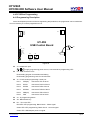
1
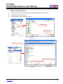
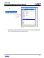
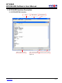
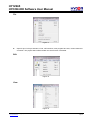
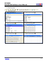
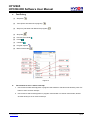
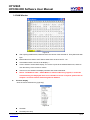
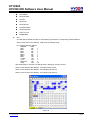
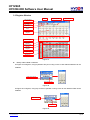
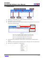
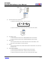
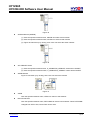
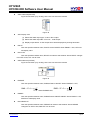
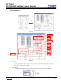
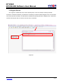
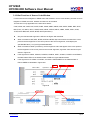
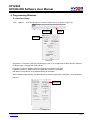
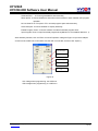
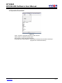
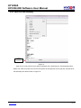
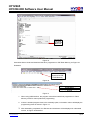
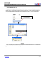
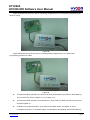
HY12S65 HYCON-IDE Software . © 2012 HYCON Technology Corp. www.hycontek.com User Manual APD-HYIDE009-V01_EN HY12S65 HYCON-IDE Software User Manual Table of Contents 1. HYCON-IDE OVERVIEW ................................................................................................4 1.1 INTRODUCTION .............................................................................................................4 1.2 HYCON-IDE INSTALLATION AND SYSTEM REQUIREMENT ................................................4 1.3 INSTALL AND REMOVE ...................................................................................................5 Install ........................................................................................................................................................ 5 Remove..................................................................................................................................................... 8 1.4 REGISTRATION..............................................................................................................8 1.5 DEMO CODE DESCRIPTION ..........................................................................................10 2. HYCON-IDE INTERFACE DESCRIPTION....................................................................12 2.1 HYCON-IDE EDIT INTERFACE ....................................................................................12 Edit Window ........................................................................................................................................... 13 File .......................................................................................................................................................... 14 Edit .......................................................................................................................................................... 14 View......................................................................................................................................................... 14 Assemble & Run .................................................................................................................................... 15 Interface Setup....................................................................................................................................... 15 . Windows................................................................................................................................................. 19 Program Structure................................................................................................................................. 19 Self-defined Instruction ........................................................................................................................ 19 3. HYCON-IDE DEBUG INTERFACE ...............................................................................21 3.1 FAST EXECUTION ........................................................................................................22 3.2 RAM WINDOW ...........................................................................................................25 3.3 REGISTER WINDOW ....................................................................................................28 3.4 WATCH WINDOW ........................................................................................................30 3.5 STACK WINDOW .........................................................................................................32 3.6 ADC WINDOW ............................................................................................................33 3.7 POWER WINDOW ........................................................................................................38 3.8 MPN WINDOW ...........................................................................................................40 3.9 REGISTER RECORD.....................................................................................................45 3.10 HINT FUNCTION OF SOURCE CODE WINDOW ...............................................................47 4. PROGRAMMING WINDOWS........................................................................................49 4.1 INTERFACE SETUP ......................................................................................................49 4.2 OPERATION PROCEDURES ...........................................................................................51 4.2.1 Open File and Assembly.............................................................................................................. 52 4.2.2 Download HEX File....................................................................................................................... 55 © 2012 HYCON Technology Corp www.hycontek.com APD-HYIDE009-V01_EN Page 2 HY12S65 HYCON-IDE Software User Manual 4.3 PC ONLINE OTP PROGRAMMING .................................................................................56 4.3.1 Blank Check .................................................................................................................................. 57 4.3.2 Program......................................................................................................................................... 57 4.3.3 Verify.............................................................................................................................................. 58 4.3.4 Read............................................................................................................................................... 58 4.3.5 AUTO.............................................................................................................................................. 60 4.4 PC OFFLINE PROGRAMMING .......................................................................................61 4.4.1Programming Description ............................................................................................................ 61 4.4.2 Program Times Restriction ......................................................................................................... 64 5. TROUBLESHOOTING ..................................................................................................64 5.1HYCON-IDE EXECUTION PROBLEM .............................................................................64 6.REVISION HISTORY......................................................................................................64 . © 2012 HYCON Technology Corp www.hycontek.com APD-HYIDE009-V01_EN Page 3 HY12S65 HYCON-IDE Software User Manual 1. HYCON-IDE Overview 1.1 Introduction To facilitate the process of product development, HYCON-IDE platform is provided to develop the full range of HYCON MCUs. Customers can implement in-circuit emulation of the end-products on this platform and program the code onto OTP products of HY series. 1.2 HYCON-IDE Installation and System Requirement Minimum requirements for operating HYCON-IDE: PC Hardware Request: PC compatible machine with PENTIUM® CPU 128 MB Memory (256MB is recommended) 10 GB Hard Disk Space Supporting Products: -HY12P65 Supporting Hardware Model No.: . -HY12S65-DK01 development kit Supporting Software Version: HY-CON IDEDMM V1.1 and above Compatibility of Program Version: N/A © 2012 HYCON Technology Corp www.hycontek.com APD-HYIDE009-V01_EN Page 4 HY12S65 HYCON-IDE Software User Manual OS: Windows 98SE Windows 2000 Windows XP Windows Vista Windows 7 Support x86, 32bit system, 64bit system not in support. Applicable Interface: USB Port 1.3 Install and Remove Install Note: For some Windows OS, it may require to have administrator identity to install the Hex Loader to the computer. Insert the HYCON-IDE CD into the CD ROM drive and find the file in the CD ROM or file to execute Setup.exe. Following the instruction window dialogs step by step to continue setup procedures. As shown in Figure 1-1. . First-time installation must initiate USB driver program, the setup procedures are as Figure 2 shown. © 2012 HYCON Technology Corp www.hycontek.com APD-HYIDE009-V01_EN Page 5 HY12S65 HYCON-IDE Software User Manual . Figure 1 © 2012 HYCON Technology Corp www.hycontek.com APD-HYIDE009-V01_EN Page 6 HY12S65 HYCON-IDE Software User Manual . Figure 2 © 2012 HYCON Technology Corp www.hycontek.com APD-HYIDE009-V01_EN Page 7 HY12S65 HYCON-IDE Software User Manual Remove Please remove the file of “HYCON-IDEDMM V1.1” in “Add/Remove Program” under Control Panel. 1.4 Registration For first time using ICE for simulation or program OTP chip, users must apply for a register code as to proceed operation. Figure 3 Registration Procedures: 1. Please check the HyIDE Machine Number (HyIDE Code) on the parcel and send the number by e-mail or on-line registration. HYCON will send back another customer register code to you. 2. Connect the HyIDE Control Board to PC through USB interface. 3. Execute HYCON-IDE software (HYCONIDE.exe). Go to ”Option” and press ”Register”. 4. Fill in the customer code in “Register Number” and click “Write” to start. . Figure 4 5. If the process is successful, a dialog will be shown as follows. Figure 5 © 2012 HYCON Technology Corp www.hycontek.com APD-HYIDE009-V01_EN Page 8 HY12S65 HYCON-IDE Software User Manual 6. If the process failed, a dialog will be shown as Figure 6. Figure 6 7. Once the register is succeeded, Customers do not have to worry that other numbers may be written into the “Register Number” . © 2012 HYCON Technology Corp www.hycontek.com APD-HYIDE009-V01_EN Page 9 HY12S65 HYCON-IDE Software User Manual 1.5 Demo Code Description Starting C:\Program Files\HyIDE\HyconIDEDMM\DemoCode\Ref Code\Test.asm Set the file as assembly main file Assembly start and proceed program debug Select Test.asm Open Demo Code Open Demo Code Figure 7 . Set as assembly main file Make sure ICE was connected Display assembly main file name Figure 8 © 2012 HYCON Technology Corp www.hycontek.com APD-HYIDE009-V01_EN Page 10 HY12S65 HYCON-IDE Software User Manual Assembly and start debugging Debugging Figure 9 . Users can use any compiler to edit Source Code, as long as it can be stored in ASCII Code format. Source code will be reloaded when program compiles to ensure its correctness. Debugging and edit function will be depicted respectively in the following chapters. © 2012 HYCON Technology Corp www.hycontek.com APD-HYIDE009-V01_EN Page 11 HY12S65 HYCON-IDE Software User Manual 2. HYCON-IDE Interface Description 2.1 HYCON-IDE Edit Interface IC No. IDE Interface Project Name . Main program file name IDE connecting status Checksum after compiled Figure 10 © 2012 HYCON Technology Corp www.hycontek.com APD-HYIDE009-V01_EN Page 12 HY12S65 HYCON-IDE Software User Manual Edit Window Open file Open the existing edited file in the disk Set bookmark Using this function to go back to the bookmark instantly when many files were opened Go to bookmark Jump to the default bookmark Find string Find input string Find next string Go to page Using this function to switch files Assemble Only acting assemble function not debug status. After assembled, a message window will show up . © 2012 HYCON Technology Corp www.hycontek.com APD-HYIDE009-V01_EN Page 13 HY12S65 HYCON-IDE Software User Manual File Figure 11 Open Project Project includes, IC No., IDE interface, main program file name, current status and checksum. The project status will be loaded once this function is activated. Edit . Figure 12 View Figure 13 © 2012 HYCON Technology Corp www.hycontek.com APD-HYIDE009-V01_EN Page 14 HY12S65 HYCON-IDE Software User Manual Assemble & Run Figure 14 Assemble & Run (Emulation) Assemble Source Code and execute debug mode Assemble Only executing assemble, not debugging. Error message will show up when the lines is error. It is usually used in generating OBJ Code (Object). Set Main File Set the file as assembly main file. Files will be named after compiler generated file name, such as Hex, MAP, ASC…etc. . Set Mode (Debug mode) Debug through software or hardware is selective. Interface Setup Figure 15 Interface Setup © 2012 HYCON Technology Corp www.hycontek.com APD-HYIDE009-V01_EN Page 15 HY12S65 HYCON-IDE Software User Manual Figure 16 Chip Select: Select IC part no. Compiler will assemble the selected part no.’s program file. It . will determine whether there is any misuse or non-existing Register or SRAM, or has the program exceeded the ROM Size. Language option: English and Chinese interface are selectable. Communication interface option: Select IDE communication interface. Mode option: Two choices, Emulate and debug, and programmer. © 2012 HYCON Technology Corp www.hycontek.com APD-HYIDE009-V01_EN Page 16 HY12S65 HYCON-IDE Software User Manual Build Option Figure 17 . Assembler generated extension: it is selectable to produce below file formats. 1. Binary file : Hex 2. Obj file : obj 3. List file: lst 4. ADCII file: asc Font option: Choose editor’s fonts. Fill unused zone: Fill the unused zone with 0x0000 or 0xFFFF in the program. Simplified assemble: Simplified assemble function is selectable. When JMP or CALL is smaller than 2K, it will automatically transform to RJ or RCALL. If the arguments of CALL are set, it will not transform to RCALL. Program protection: Please refer to “Interface Setup” under Programming Window chapter. © 2012 HYCON Technology Corp www.hycontek.com APD-HYIDE009-V01_EN Page 17 HY12S65 HYCON-IDE Software User Manual Interrupt Setup Figure 18 Stop operation when Stack overflow: IDE will stop when Stack overflow. Monitor address: Select the monitored Register or RAM. The program will stop when the . program executed RAM or Register value equals to the monitored Data. Monitor Data: Monitor value is set when the monitor Data is filled up. Monitor RAM bit: Monitor function will be activated if the monitor bit is ticked. The program will stop when the bit of Data value equals to the marked on bit. ICE Test Figure 19 © 2012 HYCON Technology Corp www.hycontek.com APD-HYIDE009-V01_EN Page 18 HY12S65 HYCON-IDE Software User Manual Windows The window can be displayed horizontally or vertically. Figure 20 Program Structure Before editing new program, user must select IC part number through interface setup; Different IC will have different Instruction Set, according to IC part number definition; it is classified as H08A and H08B instruction set; User can refer to the appendix software demo code, Chapter 1.6 gives illustration of demo code usage. Users can refer to following program structure to start writing program. Basic structure description is listed as below: Program Name Definition as: ***.ASM Register Name or RAM Definition as: ***.INC Two program contectents are listed below: “Test.asm”& “H08.inc” ; Program name can be any name ; Special register names and address definition of HY12P series ; Declare program start ; Jump to main program ORG NOP RET ; Declare interrupt flag address ; Interrupt program START: CALL IDLE NOP 04H ; Start Main program. Label name definition can be any word DELAY DELAY: . . . RET END . “Main.asm” structure: Include H12P.inc ORG 00H JMP START ; End Program Reference Document: IP User Manual: User’s Guide Instruction Set User Manual: H08A Instruction Set Manual HYCON-IDE Complier User Manual: HY-MCU COMPILER Self-defined Instruction HYCON-IDE for DMM includes user self-defined instruction function This function provides user to self-define HY12P series instruction as their familiar MCU instructions. © 2012 HYCON Technology Corp www.hycontek.com APD-HYIDE009-V01_EN Page 19 HY12S65 HYCON-IDE Software User Manual Usage description: 1. All self-defined instruction function is installed under: Inst.txt file. It is separated into two rows. The first instruction (first row) of every row is HYCON origin instruction name; users cannot make amendment to it. The second instruction (second row) is "User" self-defined instruction name. 2. First and second instruction can only be separated by space, multi-space or Tab. 3. Second instruction can be followed by semicolon (;) as remark. 4. Second instruction name can be the same as the first one. 5. The name of second instruction cannot be defined as any of HYCON origin instruction name except the instruction in the same row. Otherwise, it is deemed as invalid and will adopt the origin instruction name to compile program. 6. After users self-define the second instruction name, the first or second instruction name can be used when program compiling. 7. Every row can only has one self-defined instruction name, any repeated instruction name will be deemed as invalid. For example: JMP JUMP JMM JPP JU ;╳wrong definition way JMP JUMP Repeated defined instruction or self-define instruction will be deemed as invalid. Example: . JMP JUMP JMP JPP ;╳ instruction name redefine. JUMP will be deemed as invalid instruction, only JPP is JU ;╳ cannot use self-defined name to redefine valid. JPP JMP JN ;╳ cannot be defined as HYCON origin existed instruction name Correct definition is: JMP JUMP © 2012 HYCON Technology Corp www.hycontek.com APD-HYIDE009-V01_EN Page 20 HY12S65 HYCON-IDE Software User Manual 3. HYCON-IDE Debug Interface It can be classified into hardware debug and software debug. Hardware debug The indication column is blue Software debug The indication column is green . © 2012 HYCON Technology Corp www.hycontek.com APD-HYIDE009-V01_EN Page 21 HY12S65 HYCON-IDE Software User Manual 3.1 Fast Execution (1) (3) Fast window switch Switch to Edit window Switch to Hex window (2) Switch to Source window (4) Switch to Ram window (6) Switch to Watch window . (5) Switch to Reg window © 2012 HYCON Technology Corp www.hycontek.com APD-HYIDE009-V01_EN Page 22 HY12S65 HYCON-IDE Software User Manual Fast Debug (1) Step back (2) Trace (Enter into Macro/vice program) (3) Step over (Not enter into Macro/vice program) (4) Skip Call (5) Execute (Free RUN) (6) Pause (7) Continue (8) Program replace (9) Back to edit mode . Figure 21 Two methods to set or remove interrupt: 1. Use mouse to select interrupt place in program code window or machine code window, press “F2” button to set to remove interrupt. 2. Use mouse to select interrupt place in program code window or machine code window, double click the left key to set or remove interrupt. © 2012 HYCON Technology Corp www.hycontek.com APD-HYIDE009-V01_EN Page 23 HY12S65 HYCON-IDE Software User Manual . Figure 22 © 2012 HYCON Technology Corp www.hycontek.com APD-HYIDE009-V01_EN Page 24 HY12S65 HYCON-IDE Software User Manual 3.2 RAM Window Figure 23 After opening RAM window, Bank will show the volume of the selected IC. Every Bank has 256 byte. . Bank0 starts from 0x00 to 0xFF. Bank1 starts from 0x100 to 0x1FF…etc. If the address does not exist, it will display “-”. If users intend to switch Bank display, use cursor to point to the desired Bank zone, and then click the left key of the mouse to confirm. If Hint is set, the address will display numbers and will be underlined. Notice: The Address 0x00 ~ 0x0Eof Bank0 is indirect addressing register, it cannot be revised directly, the displayed value is not referable. If revise is required, please refer to Chapter 3.3. Revise indirect addressing Data or Address. Function Display Click the mouse selection key (right key) Figure 24 Set Mark Set Mark(new color) © 2012 HYCON Technology Corp www.hycontek.com APD-HYIDE009-V01_EN Page 25 HY12S65 HYCON-IDE Software User Manual Reset Mark Reset All Mark Set Hint Reset Hint Reset All Hint Load RAM Data Save RAM Data Save To excel RAMBANK0 Hint Use DS defined SRAM; Hint will be automatically generated in corresponding window address. When cursor point to the address, it will show the defined string. Ex: Program definition SRAM MEMAR 080h MD1 DS 1 MD2 DS 1 MD3 DS 1 MDL1 DS 1 MDL2 DS 1 MDL3 DS 1 MD4 DS 5 S_REG DS 1 r_Len DS 1 SQRTmp DS 4 Temp DS 16 After assembling, it will enter into debug status, displaying memory window. . When cursor points to 80h address, <80>:MD1 will be shown. When cursor points to 86h address, <86>:MD4[0] will show up. When cursor points to 87h address, <87>:MD4[1] will show up. Figure 25 © 2012 HYCON Technology Corp www.hycontek.com APD-HYIDE009-V01_EN Page 26 HY12S65 HYCON-IDE Software User Manual There are two ways to revise SRAM value 1. Point the cursor to the selected revised lines, click mouse’s left key and Key IN directly. 2. Point the cursor to the selected revised lines, double click the mouse’s left key, a window will pop up as Figure 27 shown. Users can key in on keyboard or press the button by mouse Figure 26 . © 2012 HYCON Technology Corp www.hycontek.com APD-HYIDE009-V01_EN Page 27 HY12S65 HYCON-IDE Software User Manual 3.3 Register Window WREG Program Counter Cycle Times Data of indirect address 0 Address of indirect data 0 Data of indirect address 1 Address of indirect data 1 Single Byte Register 1 Word Register Display PAGE1 Register Display PAGE2 Register Display PAGE3 Register Register byte Register bit . Figure 27 Modify Indirect Data or Address As Figure 28 configures, using keyboard to Key IN or using cursor to click data the Address can be modified. Modify Indirect Address Using cursor to click 1 Figure 28 As Figure 29 configures, using Key IN of the keyboard or using cursor to click data the Data can be modified. Modify indirect Data Click 1 Figure 29 © 2012 HYCON Technology Corp www.hycontek.com APD-HYIDE009-V01_EN Page 28 HY12S65 HYCON-IDE Software User Manual Modify WREG Data Modify WREG Data Click Figure 30 Modify Data of single 1byte or Word Register Double click the mouse’s left key, a input interface will show up Click Zone Using keyboard to Key In directly . Figure 31 Modify Register single 1 byte or single 1 bit After configuring Bit as 1, it will be highlighted in white, blue digit After configuring Bit as 0, it will be marked in black digit 滑鼠左鍵連續點擊2次 滑鼠左鍵連續點擊2次 出現數值輸入畫面 出現數Bit設置畫面 Figure 32 © 2012 HYCON Technology Corp www.hycontek.com APD-HYIDE009-V01_EN Page 29 HY12S65 HYCON-IDE Software User Manual 3.4 Watch Window Watch Address Watch Name Watch Data for Bin Watch Data Data Type Data Length Figure 33 Watch Name Monitor Data name, program uses EQU or DS defined name Watch Address Monitor Data Address Watch Data Display value, can select display arrangement from right to left or from left to right or in decimal or hexadecimal system. 4 options will show up after clicking . Move the mouse to here and double clicking Figure 34 Hex (H L): Hexadecimal display, address H/L from low to high Hex (L H): Hexadecimal display, address L/H from high to low Dec (H L): Decimal display, address H/L from low to high Dec (L H): Decimal display, address L/H from high to low Watch Data for Bin Data display in decimal system, only show up when using EQU defined address Data Length Data length, display DS definition length; it will display 2 when using EQU definition Data Type D = DS definition; C = EQU definition © 2012 HYCON Technology Corp www.hycontek.com APD-HYIDE009-V01_EN Page 30 HY12S65 HYCON-IDE Software User Manual Monitor EQU defined Register or RAM, click right key of the mouse and select the register or RAM to be monitored, as shown in Figure 35. Figure 35 . © 2012 HYCON Technology Corp www.hycontek.com APD-HYIDE009-V01_EN Page 31 HY12S65 HYCON-IDE Software User Manual 3.5 Stack Window Figure 36 . Figure 37 © 2012 HYCON Technology Corp www.hycontek.com APD-HYIDE009-V01_EN Page 32 HY12S65 HYCON-IDE Software User Manual 3.6 ADC Window Click ADC Panel Figure 38 AD1IP Network AD1IN Network AD1CHO PNetwork AD1 INPBUFF ENADC ADCCK selection . VRGN ADGN Network AD1FP Network AD1 VRBUFF AD1FN Network AD1RH Network Reset Comb Filter AD1RL Network OSR1 Network LPF output button Display ADC value Display LPF Reset RMS LPF ADC output button ADC output bit number ADC output type Reset LPF OSR4 ENLPF Network Root/Absolute ENRMS Figure 39 © 2012 HYCON Technology Corp www.hycontek.com APD-HYIDE009-V01_EN Page 33 HY12S65 HYCON-IDE Software User Manual AD1IP Network (ADSIP) (1) Click the network name, then AD1IP can go to the specified network (2) Click it and Figure 40 will be displayed Figure 40 AD1IN Network (ADSIN) (1) Click the network name, then AD1IN can go to the specified network (2) Click it and Figure 41 will be displayed Figure 41 AD1FP Network (ADSFP) . (1) Click the network name, then AD1FP can go to the specified network (2) Click it and Figure 42 will be displayed Figure 42 AD1FN Network (ADSFN) (1) Click the network name, then AD1FN can go to the specified network (2) Click it and Figure 43 will be displayed © 2012 HYCON Technology Corp www.hycontek.com APD-HYIDE009-V01_EN Page 34 HY12S65 HYCON-IDE Software User Manual Figure 43 AD1CHOP Network switch (ADSCHP) (1) Network is switchable by clicking, 3 types are selective (2) Figure 44 will show up by clicking, then users can select the switch network . Figure 44 AD1 INPBUFF switch (1) Click the specified network name, ADSIPB/ADSINB switch will be ON/OFF (2) Click the specified network switch, ADSIPB/ADSINB switch will be ON/OFF ADCCK option Click the specified network name, ADCCK will switch options. When ADCCK = OFF, HAO_OSC/10. When ADCCK = ON, HAO_OSC/20. ENADC Click the specified network name, ENADC will be ON/OFF. When ENADC = ON, ADC zone will display value AD1RH Network (ADSRP) (1) Click the specified network name, AD1RH can select to that network (2) Click the specified network switch , AD1RH can select to that network (3) Figure 45 will show up by clicking, then users can select the switch network © 2012 HYCON Technology Corp www.hycontek.com APD-HYIDE009-V01_EN Page 35 HY12S65 HYCON-IDE Software User Manual Figure 45 AD1RN Network (ADSRN) (1) Click the specified network name, AD1RN can select to that network (2) Click the specified network switch, AD1RN can select to that network (3) Figure 46 will show up by clicking, then users can select the switch network . Figure 46 AD1 VRBUFF Switch (1) Click the specified network name, P_VERBUFF/N_VERBUFF switch will be ON/OFF (2) Click the specified network switch, P_VERBUFF/N_VERBUFF switch will be ON/OFF ADGN Network Figure 47 will show up by clicking, then users can select the network Figure 47 VRGN Click the specified network name, VRGN can select to that network Reset Comb Filter Click the specified network name, RSTCOMB can select to that network. When RSTCOMB changed from OFF to ON, Comb Filter can be reset. © 2012 HYCON Technology Corp www.hycontek.com APD-HYIDE009-V01_EN Page 36 HY12S65 HYCON-IDE Software User Manual OSR1 Network(ADFOSR) Figure 48 will show up by clicking, then users can select the network Figure 48 ADC Display zone (1) Select ADC data output type Hex or Dec output (2) Select ADC data output Bit From 8 ~ 19 Bit output (3) Display output button ADC output value will be displayed by clicking this button ENLPF Click the specified network name, ENLPF will be ON/OFF. When ENADC = ON, LPF zone will display value Reset LPF Click the specified network name, RSLPF can select to that network. When RSLPF changes from OFF to ON, LPF can de reset. OSR4 Network (LPFBW) . Figure 49 will show up by clicking, then users can select the network Figure 49 ENSQUE Click the specified network name, ENSQUE will be ON/OFF. When ENSQUE = OFF, 2 RMS 37 : 0 RMS 37 : 0 X N . When ENSQUE=ON, X N . ENRMS Click the specified network name, ENRMS will be ON/OFF.ON/OFF. When ENADC = ON, RMS zone will display value. Reset RMS LPF Click the specified network name, RSRMS can select to that network. When RSRMS changes from OFF to ON, RMS LPF can be reset. © 2012 HYCON Technology Corp www.hycontek.com APD-HYIDE009-V01_EN Page 37 HY12S65 HYCON-IDE Software User Manual 3.7 Power Window Figure 50 LDO Network ENLDO ENVGG . VLCD Network LCDPR ENLCD LCDBF ENREFO AGND Net work SREFO Figure 51 ENLDO Click the specified network name, ENLDO will be ON/OFF. ENLDO display status, when ENLDO = 1, VDDA output voltage. LDO Network Figure 52 will show up by clicking, and then users can select the switch network Figure 52 © 2012 HYCON Technology Corp www.hycontek.com APD-HYIDE009-V01_EN Page 38 HY12S65 HYCON-IDE Software User Manual ENVGG Click the specified network name, ENVGG will be ON/OFF. ENVGG display status, when ENVGG = 1, VGG output voltage ENLCD Click the specified network name, ENLCD will be ON/OFF. ENLCD display status, when ENLCD = 1, start LCD LCDPR Click the specified network name, LCDPR will be ON/OFF. LCDPR display status, when LCDPR= 1, VLCD power sauce is generated from internal IC. When LCDPR= 0, VLCD power sauce is generated from external input pin LCDBF Click the specified network name, LCDBF will be ON/OFF. LVDBF display status. VLCD Network Figure 53 will show up by clicking, and then users can select the switch network . Figure 53 ENREFO Click the specified network name, ENREFO will be ON/OFF. ENREFO display status, when ENREFO = 1, REFO output voltage SREFO Click the specified network name, SREFO will be ON/OFF, SREFO display status. When SREFO= 1, REFO power sauce is generated from internal IC. When SREFO= 0, REFO power sauce is generated from external PB< 4 > pin AGND Network Figure 54 will show up by clicking, and then users can select the switch network Figure 54 © 2012 HYCON Technology Corp www.hycontek.com APD-HYIDE009-V01_EN Page 39 HY12S65 HYCON-IDE Software User Manual 3.8 MPN Window Clicking MPN Figure 55 . Measurement Mode Network VREF Network ENCMP Multifunction Network VRHCMP Network INCMP Network VRLCMP Network Figure 56 © 2012 HYCON Technology Corp www.hycontek.com APD-HYIDE009-V01_EN Page 40 HY12S65 HYCON-IDE Software User Manual ENCMP Click the specified network name, ENCMP will be ON/OFF, ENCMP display status. INCMP Network (1) Click the specified network name, INCMP can select to that network (2) Click the specified network switch, INCMP can select to that network (3) Figure 57 will show up by clicking, and then users can select the switch network Figure 57 VRHCMP Network (1) Click the specified network name, VRHCMP can select to that network (2) Click the specified network switch, VRHCMP can select to that network . (3) (4) Figure 58 will show up by clicking, and then users can select the switch network Figure 58 © 2012 HYCON Technology Corp www.hycontek.com APD-HYIDE009-V01_EN Page 41 HY12S65 HYCON-IDE Software User Manual VRLCMP Network (1) Click the specified network name, VRLCMP can select to that network (2) Click the specified network switch, VRLCMP can select to that network (3) Figure 59 will show up by clicking, and then users can select the switch network Figure 59 VREF Network (1) Click the specified network name, VREF can select to that network (2) Click the specified network switch, VREF can select to that network (3) Figure 60 will show up by clicking, and then users can select the switch network . Figure 60 Measurement Mode Network (1) Click the specified network name, users can select to that network (2) Click the specified network switch, users can select to that network (3) Figure 61 will show up by clicking, and then users can select the switch network Figure 61 © 2012 HYCON Technology Corp www.hycontek.com APD-HYIDE009-V01_EN Page 42 HY12S65 HYCON-IDE Software User Manual Multi-function Network (1) Click the specified network switch, users can select to that network (2) Figure 62 will show up by clicking, and then users can select the switch network . © 2012 HYCON Technology Corp www.hycontek.com APD-HYIDE009-V01_EN Page 43 HY12S65 HYCON-IDE Software User Manual Figure 62 . © 2012 HYCON Technology Corp www.hycontek.com APD-HYIDE009-V01_EN Page 44 HY12S65 HYCON-IDE Software User Manual 3.9 Register Record If the register or SRAM has been revised manually after access to simulation window (hardware emulation or software simulation), the data will be recorded (no matter the RAM, Register, ADC, OP and CMP was revised by which window). The data will be revealed after pressing the button “SRAM record”. At this time, windows will suspend until it is closed to execute other commands. Display SRAM & Register record . Figure 63 © 2012 HYCON Technology Corp www.hycontek.com APD-HYIDE009-V01_EN Page 45 HY12S65 HYCON-IDE Software User Manual Add To Program PC Stop Address . Add New Program Figure 64 © 2012 HYCON Technology Corp www.hycontek.com APD-HYIDE009-V01_EN Page 46 HY12S65 HYCON-IDE Software User Manual 3.10 Hint Function of Source Code Window If users intend to know Register or SRAM value and Address in source code window, point the cursor to Register or SRAM, the name, address and data can be revealed. This function is only applicable to the instructions below: CLRF, ADDF, INF, INSZ, DCF, DCSZ, SUBF, COMF, ADDC, ANDF, IORF, XORF, SUBC, RRF, SETF, MULF, RLF, JZ, RRFC, RLFC, SWPF, DAW, INSUZ, DCSUZ, ARLC, ARRC, CPSG, CPSL, CPSE, TFSZ, BTFG BSF, BCF, BTSS, BTSZ, MVFF (Not Macro). Only the first followed argument is effective as Figure 655 described. When command is BCF, BSF, BTSS, BTSZ and BTGF, Byte value will be revealed if the cursor points to the first argument. If the cursor points to the second argument, it will display the specified Bit value (1 or 0) as Figure 666 illustrated. When command is MVFF (not Macro), the first argument value will appear if the cursor points to the first argument. If the cursor points to the second argument, argument value will show up as shown in Figure 67. If the argument is INDF0, POINC0, PODEC0, PRINC0, INDF1, POINC1, PODEC1 and PRINC1, the Data will be FSR0 or the address Data of FSR1 as Figure 688 described. . If the argument is PLUSW0 or PLUSW1, the Data is FSR0+WREG or the address Data of FSR1+WREG as illustrated in Figure 699. Name Address Data Figure 65 Display bit Display Byte Figure 66 © 2012 HYCON Technology Corp www.hycontek.com APD-HYIDE009-V01_EN Page 47 HY12S65 HYCON-IDE Software User Manual Display the first Argument Display the second Argument Figure 67 Name FSR0 Address Data Figure 68 Name FSR0+WREG Address . Data Figure 69 © 2012 HYCON Technology Corp www.hycontek.com APD-HYIDE009-V01_EN Page 48 HY12S65 HYCON-IDE Software User Manual 4. Programming Windows 4.1 Interface Setup Click “Options”, a window will appear. Click the interface setup, as shown in Figure 70. . Figure 70 Chip Select Choose the specific programming IC part no. If programmed IC differs from the selected IC, Blank Check, Program and Verify will fail. Language Choose operation interface language, like Chinese or English. Hardware Interface USB interface or Parallel Port interface is selectable. IDE Mode Programmer or emulate and Debug is selectable. When interface setup finished, click Build Options to select programming configuration. As described in Figure 71. Figure 71 © 2012 HYCON Technology Corp www.hycontek.com APD-HYIDE009-V01_EN Page 49 HY12S65 HYCON-IDE Software User Manual Generate Files Choose generated file after assembly Stack Option Choose whether to reset when stack overflow or stack full after OTP program operation. No Use Area Fill Fill up 00 or FF in unused program space after assembly. Smart Compiler Choose whether to simplify assembly. Enable Program Times Choose whether to enable Download program times. Input Program Times Input Download program times (Maximum: 2147483646. Minimum: 1). After assembly finished, click “ICE Test” to test ICE operation voltage as Figure 72 (Connect Adapter 9V and connect USB Line to ICE. Make sure the ICE is connected, and then click “Option”). 顯示VPP電壓 檢查VPP電壓 顯示VDD電壓 檢查VDD電壓 . 檢查VPP與VDD電 壓 Figure 72 VPP voltage when programming: 5.6<VPP<6.6 VDD voltage when programming: 2.7<VDD<3.6 © 2012 HYCON Technology Corp www.hycontek.com APD-HYIDE009-V01_EN Page 50 HY12S65 HYCON-IDE Software User Manual 4.2 Operation Procedures Figure 73 Open Open the programmed source code main file. Open Project Open the saved project. Save Project Save the finished project. Download file to Flash Memory Download the finished Hex file after assembly to programmer or IDE Flash Memory. . © 2012 HYCON Technology Corp www.hycontek.com APD-HYIDE009-V01_EN Page 51 HY12S65 HYCON-IDE Software User Manual 4.2.1 Open File and Assembly . Display Assembly Main File Name Figure 74 Open source code main file and it will be displayed as the assembly file. If the displayed name differs from main file, points the mouse to the specific file and presses mouse right key. Set this file as the assembly main file as shown in Figure 75. © 2012 HYCON Technology Corp www.hycontek.com APD-HYIDE009-V01_EN Page 52 HY12S65 HYCON-IDE Software User Manual . Figure 75 Assembles Source Code and download the file to programmer or IDE Flash Memory, as Figure 76 illustrated. Assemble and download to IDE Flash Memory Figure 76 Figure 77 1. When using USB interface, the program code will be loaded into programmer or Flash Memory of IDE for mass production programming. 2. If there is enabled program times in the assembly option, information column will display the programming times as shown in Figure 77. 3. After assembling completed, Hex filename and Checksum will be displayed in underneath section, as Figure 78 illustrated. © 2012 HYCON Technology Corp www.hycontek.com APD-HYIDE009-V01_EN Page 53 HY12S65 HYCON-IDE Software User Manual Load Hex file name IC connection display zone Hex Checksum Figure 78 . © 2012 HYCON Technology Corp www.hycontek.com APD-HYIDE009-V01_EN Page 54 HY12S65 HYCON-IDE Software User Manual 4.2.2 Download HEX File To program an already assembled Hex file, go to “File” Select “Download to Flash Memory” and the Hex file. However the last option will change according to initial setup, whether to protect the program or not. If protect program was activated, the warning message will not show up, as Figure 79 described. Download the Hex file to programmer or to IDE Flash Memory . Select the Hex file to be programmed Figure 79 When download success, message column will display successful message, as Figure 77 illustrated and display Download Hex file and Checksum, as Figure 78. © 2012 HYCON Technology Corp www.hycontek.com APD-HYIDE009-V01_EN Page 55 HY12S65 HYCON-IDE Software User Manual 4.3 PC Online OTP Programming Figure 80 Figure 81 Blank Check, Programming, Verify and Read Commands can be implemented when the programmed file being successfully loaded into programmer or IDE Flash Memory. On the contrary, those commands will not be activated if the download failed. . Figure 82 Figure 83 OTP not connected Figure 84 Make sure the selected programming IC part number is the same with the OTP part number in the topic window as Figure 70 described. When programmer executes Blank Check, Programming and Verify commands, program will check whether the IC part number and OTP programming part number are identical. If the part number is different, the data will not be written into OTP and an error message will be displayed in information column as Figure 82 described. If users intend to find out whether the part number is correct before programming, point the cursor to ”IC Connection Status Display” and click the mouse left key. If the selected IC is correct, a message © 2012 HYCON Technology Corp www.hycontek.com APD-HYIDE009-V01_EN Page 56 HY12S65 HYCON-IDE Software User Manual will show up as Figure 83. If it is incorrected, the message will be displayed as Figure 88. If “Enable Program Times” has been marked up, the spare program times will display in the message column as Figure 85 illustrated. Figure 85 4.3.1 Blank Check Blank Check icon is . The internal code of Blank ICs that have yet been programmed is 0xFFFF. The purpose of checking the IC is to make sure the OTP address content is 0xFFFF. If the IC selection is correct and the content is empty, a message will appear as Figure 86. Figure 86 . If the IC selection is incorrect or the content is not empty, a message will show up as Figure 87. Figure 87 4.3.2 Program The icon of Program is . The purpose of programming is to write Compiler accomplished program into IC OTP. When programming is completed and the IC is assembled as finished goods, programmer can operate the program as user commanded. Program the downloaded or assembly finished Hex file (displayed at the bottom of the column) in the selected IC and verify the correctness of the programming content (please refer to Chapter 4.2.1 or 4.2.2 for programming procedures). If the selected IC is correct and the programming succeeds, message will appear at the information column as Figure 88 illustrated. If “Enable Program Times” is ticked up, the enable program times will minus 1 and the program times left will be revealed in the message column. © 2012 HYCON Technology Corp www.hycontek.com APD-HYIDE009-V01_EN Page 57 HY12S65 HYCON-IDE Software User Manual Figure 88 If the IC selection is incorrect or the programming fails, a message will show up as igure 89. igure 89 4.3.3 Verify The icon of Verify is . The purpose to verify .programming IC is to compare if the program written into IC OTP equals to the program downloaded to programmer or IDE Flash Memory. Verify programming IC content consistency with the downloaded or assembled Hex file (displayed at the bottom of the column). If the IC is protected by program, this verification is ineffective or the comparison failed. If IC selection and program verification is success, a message will appear as Figure 90. Figure 90 If IC selection is incorrect or the program verification miscarries, a message will pop up as Figure 91. Figure 91 4.3.4 Read The icon of Read is . The purpose to read the IC is to verify the consistency of OTP Checksum and programmed Hex file. To read IC content, the procedures are illustrated as Figure 92. Its content will reveal at ”Display Code” window. © 2012 HYCON Technology Corp www.hycontek.com APD-HYIDE009-V01_EN Page 58 HY12S65 HYCON-IDE Software User Manual If the IC is protected by program, this function is ineffective or the comparison failed. Figure 92 . © 2012 HYCON Technology Corp www.hycontek.com APD-HYIDE009-V01_EN Page 59 HY12S65 HYCON-IDE Software User Manual 4.3.5 AUTO The icon of Auto is . Auto integrates Blank Check, Program and Verify function. If user selects Auto, it will first check whether the IC is blank, then to program and verify. After the execution succeeded, a message will be displayed as Figure 93 displayed. If the option, ”Enable Program Times” is ticked up, the program permitted times will reduce 1 and the program times left will be shown in the message column. Figure 93 If any function fails, the whole process will stop and display an error message in the message column. . © 2012 HYCON Technology Corp www.hycontek.com APD-HYIDE009-V01_EN Page 60 HY12S65 HYCON-IDE Software User Manual 4.4 PC Offline Programming 4.4.1Programming Description As the development process evolves to engineering trial production, the programmer can be used alone. It is not necessary to connect programmer to PC. VSS 4 6 2 1 3 5 ICESCK VDD ICESDI ICESDO U7 ICECS J1 HY-IDE USB Control Board J5 1 2 3 4 9V VPP (6V) Ground ICESCK ICESDI ICESDO 5 VDD (3V) 6 VSS S2 Blank Check D4 J4 S1 Program . Figure 94 J4 : Adapter 9V input supply programming power source, connected when programming OTP U7 : USB connector to PC Downloading program for emulation and debug Downloading programming code for HY12P series J5 : HY12P series programming control port PIN 1 VPP(6V) connects to VPP of the IC PIN 2 ICECK connects to PSCK of the IC PIN 3 ICESDI connects to PSDI of the IC PIN 4 ICESDO connects to PSDO of the IC PIN 5 VDD(3V) connects to VDD of the IC PIN 6 VSS connects to VSS of the IC S1 : IC programming button S2 : Blank Check key D4 : Two-color LED; Red LED: OTP programming, Blank Check…failure signal. Green LED: OTP programming, Blank Check…success signal. Green LED: USB/Adapter power-on signal. © 2012 HYCON Technology Corp www.hycontek.com APD-HYIDE009-V01_EN Page 61 HY12S65 HYCON-IDE Software User Manual Figure 95 shows the connection way of connecting programming IC to control board programming pin when PC online. Figure 95 Figure 968 shows the connection way of connecting offline programming IC to control board programming pin when PC offline. . Figure 96 To implement offline operation, Hex file must be firstly downloaded to programmer Flash Memory. The procedure can refer to chapter 4.2.1 or chapter 4.2.2. To implement offline operation, press S2 button to check if the IC is blank and the D4 Green LED should be lighted up. S1 Button is programming button. Its procedures are: Blank Check Program Verify. If ”Program Protection” of “Assemble Option” is ticked before downloading data to Flash Memory, © 2012 HYCON Technology Corp www.hycontek.com APD-HYIDE009-V01_EN Page 62 HY12S65 HYCON-IDE Software User Manual program protection will be executed after Verify completed. If ”Program Protection” is not picked up, it will stop after Verify accomplished and D4 Green LED will be lighted up. When Programming finished, please press S2 to check if the IC is blank. At this moment, the D4 Red LED should be lighted up, which means the programming is successful (data has been programmed into IC, so Blank Check failed). If any failure or error happened during execution procedures, D4 Red LED will be lightened up. On the contrary, D4 Green LED will be lighted up if success. . © 2012 HYCON Technology Corp www.hycontek.com APD-HYIDE009-V01_EN Page 63 HY12S65 HYCON-IDE Software User Manual 4.4.2 Program Times Restriction The menu of ”Assemble Option” in interface setup has an option of ”Enable Program Times” as described Figure 71. This option restricts the permitted program times of download program. This is a safety mechanism that restrains the permitted program times, preventing it from over-programming on the production line. After ticking up ”Enable Program Times”, key in the program times in the column below ”Input Program Times” (maximum is 99999999, minimum is 1). This argument will be written into EEPROM of the programmer after the compiler programmed file is downloaded to Flash Memory. Afterwards, the enabled program times will reduce 1 each time when programming completed. If the value reduced to 0, the programming action may not be executed. At this time, an error signal (Red LED) will be lighted up but Blank Check still operates normally. 5. Troubleshooting 5.1HYCON-IDE Execution Problem . The problem might be happened under Microsoft Vista or Windows 7 system environment. To avoid the problem, the limit of authority for HYCON-IDE execution has to be set as system administrator to execute HYCON-IDE by administrator status. 6. Revision History Major differences are stated thereinafter: Version Page V01 ALL © 2012 HYCON Technology Corp www.hycontek.com Revision Summary First Edition APD-HYIDE009-V01_EN Page 64