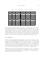
1
Autonomous Computing Systems
Neil Joseph Steiner
Dissertation submitted to the Faculty of the
Virginia Polytechnic Institute and State University
in partial fulfillment of the requirements for the degree of
Doctor of Philosophy
in
Electrical Engineering
Peter Athanas, Chair
Mark Jones
Cameron Patterson
Gary Brown
Djordje Minic
March 27, 2008
Bradley Department of Electrical and Computer Engineering
Blacksburg, Virginia
keywords: Autonomic, Hardware, Information, Interaction, FPGA
c 2008, Neil Joseph Steiner. All Rights Reserved.
Copyright Autonomous Computing Systems
Neil Joseph Steiner
Abstract
This work discusses autonomous computing systems, as implemented in hardware, and the properties required for such systems to function. Particular attention is placed on shifting the associated
complexity into the systems themselves, and making them responsible for their own resources and
operation. The resulting systems present simpler interfaces to their environments, and are able to
respond to changes within themselves or their environments with little or no outside intervention.
This work proposes a roadmap for the development of autonomous computing systems, and shows
that their individual components can be implemented with present day technology.
This work further implements a proof-of-concept demonstration system that advances the state-ofthe-art. The system detects activity on connected inputs, and responds to the conditions without
external assistance. It works from mapped netlists, that it dynamically parses, places, routes, configures, connects, and implements within itself, at the finest granularity available, while continuing
to run. The system also models itself and its resource usage, and keeps that model synchronized
with the changes that it undergoes—a critical requirement for autonomous systems. Furthermore,
because the system assumes responsibility for its resources, it is able to dynamically avoid resources
that have been masked out, in a manner suitable for defect tolerance.
Xilinx graciously supported this research by granting the author exceptional
access to confidential and proprietary information. The reader is advised
that Xilinx software license agreements do not permit reverse engineering
of the company’s intellectual property in any form.
Acknowledgements
Thanks to Dr. Peter Athanas, my reason for joining Virginia Tech and the Configurable Computing
Lab. It has been a privilege, and a tremendously rewarding experience. May Skynet never find me.
Thanks to Dr. Mark Jones, Dr. Cameron Patterson, Dr. Gary Brown, and Dr. Djordje Minic. Just
as the strength of a conference rests on its program committee, the strength of a dissertation rests
on its advisory committee.
Thanks to Mr. John Rocovich and the Bradley Foundation for funding three years of my research
as a Bradley Fellow. This forward-looking work would have been impossible to undertake without
the independent source of funding.
Thanks to Xilinx Research Labs for your tremendous support of both this work and prior related
work. I am deeply indebted and very grateful, and I remain a true believer in your products.
Thanks to Carlos Lucasius and Sun Microsystems, Inc., for allowing me to use Java SE for Embedded (PowerPC) beyond the normal trial period.
Thanks to Jeff Lindholm at Xilinx, Inc., who passed away last year. Jeff was one of the good guys.
Thanks to my past mentors: Maya Gokhale, Justin Tripp, Brandon Blodget, and James Anderson.
Thanks to Matt Shelburne and Tim Dunham for your assistance in helping me debug bitstream
and EDK issues. The issues were small, but the time saved was enormous.
Thanks to my many CCM Lab friends, and Stephen Craven in particular. It has been a real
pleasure working with so many of you, and I will remember this place with many fond memories.
Thanks to my many other friends: Eric, Ben, Tullio, Rick, J.D., James G., Amy, Jeremy, Stella,
Tim, Phil, Lauren and Lauren, Carla, Alex, Valérie, and more.
Thanks to my parents, who somehow find the time to worry about when I’ll get married; to Bern
and Camaleta, Stephanie, Eric, and Luke; and to Norine and Andrew, Jordan, Jackie, and Blaise.
Et un trés grand merci aussi à Johannes, à Véronique, et à Lili pour votre amitié. Peut-être
trouverai-je enfin le temps de rétablir notre contact.
iv
Preface
0.1
Overview
The long-term underlying question that prompted this work concerns the very nature of computation [1]: How exactly do hardware and information interact? Information is both the fundamental
ingredient of computation and its end product, and without information, computation would serve
no purpose. On the other hand, information is incapable of doing anything without an underlying
hardware substrate.
Computation is so pervasive in modern society that one might easily assume all of the foundations
to be well understood, but while we very well understand how to use computation, we are harder
pressed to explain what it is. That hardware and information do interact is well established however,
and that interaction can be observed in both microscopic1 and macroscopic behaviors.
0.2
Microscopic Behavior
The microscopic behavior of hardware and information is governed by the fundamental nature
of matter, energy, and information, and by the interactions permitted by the laws of physics [2].
Understanding of the underlying behavior does remain a long term interest of this work, but at
present the fundamental questions still lie beyond the reach of physics.
According to the quantum mechanical formalism, the wavefunction ψ of a system encodes all of the
information about the physical state of that system,2 so there is at least some known relationship
between information and the wavefunction. If one can then express a relationship between matter or
energy and the wavefunction, it should be possible by transitivity to derive a relationship between
matter, energy, and information: Perhaps some analogue or extension to Einstein’s E = mc2 which
1
The term microscopic is relaxed here to simply refer to fundamental behavior, with no assumption that this
behavior be directly observable with a microscope.
2
Some physicists are careful to speak of physical information [3], perhaps tacitly allowing that information in the
wavefunction might not be the most fundamental form of information.
v
Preface
vi
also encompasses information. Such a relationship would effectively represent governing physical
laws, and would provide a rigorous foundation for research into the nature of computation.
Unfortunately, these seemingly simple questions about relationships are in fact tremendously difficult to address. The reported successes in quantum mechanics, quantum cryptographic key exchange, and quantum teleportation, and the publicized search for answers in cosmology, string
theory, and the Theory of Everything, can convince the lay person that fundamental understanding is within reach, when there is in fact an enormous amount of work yet to be done:
• Physicists are not yet agreed on the nature of information. The Landauer view of information
as physical [4], suggests that information is actually a form of matter or energy. The Wheeler
view of information as the origin of matter and energy [5], suggests that information is a
superset of matter and energy. In both of these cases, it is reasonable to ask about the
constituent relationships, but nobody seems to be investigating these questions at present.
• Physicists are also grappling with the fundamental nature of matter and energy. Quantum
mechanics explains how particles behave as waves, and quantum field theory explains how
waves behave as particles, but nobody is sure how matter and energy relate to the wavefunction. The feeling is that string theory may suggest some geometric origin for degrees of
freedom in matter, but “at the moment nobody understands what string theory is” [6].
The present inability of physics to provide answers reflects the deep complexity of nature and the
difficulty of unraveling its mysteries, as well as the difficulty of formulating questions in a manner
conducive to answers [7]. While the most efficient way of studying hardware-information dynamics
would probably come from such answers, those answers are not available at this time.
0.3
Macroscopic Behavior
The macroscopic behavior of hardware and information governs larger scale interactions in computational circuits and systems, and is built upon the microscopic behavior, though the relationships
are presently obscured from us. On this level, it is interesting to classify systems according to the
dynamics of their state spaces. One may ask whether a system’s state space can change, and if so,
how? The underlying argument is that the dynamics of the state space have significant implications
for the flexibility and capabilities of the system.
This work implicitly acknowledges that the dynamics of the system may include hardware changes,
whether actual or virtual. At present it is possible to achieve virtual hardware changes in configurable devices such as FPGAs. Actual hardware changes will likely become possible through
continued research in nanotechnology and molecular self-assembly [8]. The meaning of the distinctions between virtual and actual changes will be presented in more detail in later chapters of this
work.
Preface
vii
Does it make sense to study macroscopic behavior if one is actually trying to understand microscopic
fundamentals? Perhaps so. In physics, it is common to study gravitational lenses, supernovae, black
holes, and cosmology—all of which are interesting in their own right—while seeking to understand
exceedingly small particles and phenomena. Certain weak physical interactions only become observable at high energies, and to study them it is often necessary to use cosmological sources or
large accelerators. This work pragmatically posits that any approach is valid if it can help shed
light on the underlying fabric of nature, particularly when other means are not available.
Another reason for studying large systems is that they tend to exhibit emergent behaviors that are
difficult or impossible to infer from fundamentals. Biology has been acquainted with Avogadroscale systems for at least as long as recorded history, and as computation progresses towards such
scales, there is an increasing effort to glean ideas and approaches from living systems. Efforts
are currently underway by Ganek and Corbi at IBM to develop autonomic systems that are selfaware, self-configuring, self-optimizing, self-healing, and self-protecting [9], and by the DARPA
Information Processing Technology Office (IPTO) to develop cognitive systems that are able to
reason, able to learn, able to communicate naturally, able to respond to unexpected situations, and
able to reflect on their own behavior [10].
While this work does not focus on artificial intelligence, it does consider the infrastructure that
might be necessary to support autonomy on large computational systems. In anticipation of
Avogadro-scale computing, it is sensible to ask how such systems might be designed, and it is
worthwhile to learn from biological systems, which do in fact grow, learn, adapt, and reason.
Table of Contents
Preface
v
0.1
Overview . . . . . . . . . . . . . . . . . . . . . . . . . . . . . . . . . . . . . . . . . .
v
0.2
Microscopic Behavior . . . . . . . . . . . . . . . . . . . . . . . . . . . . . . . . . . . .
v
0.3
Macroscopic Behavior . . . . . . . . . . . . . . . . . . . . . . . . . . . . . . . . . . .
vi
Table of Contents
vii
List of Figures
xv
List of Tables
xvii
Glossary
xx
1 Introduction
1
1.1
Overview . . . . . . . . . . . . . . . . . . . . . . . . . . . . . . . . . . . . . . . . . .
1
1.2
Autonomy . . . . . . . . . . . . . . . . . . . . . . . . . . . . . . . . . . . . . . . . . .
1
1.3
Objectives . . . . . . . . . . . . . . . . . . . . . . . . . . . . . . . . . . . . . . . . . .
3
1.3.1
Roadmap . . . . . . . . . . . . . . . . . . . . . . . . . . . . . . . . . . . . . .
3
1.3.2
Implementation . . . . . . . . . . . . . . . . . . . . . . . . . . . . . . . . . . .
3
Organization . . . . . . . . . . . . . . . . . . . . . . . . . . . . . . . . . . . . . . . .
4
1.4
viii
Table of Contents
2 Background
ix
5
2.1
Overview . . . . . . . . . . . . . . . . . . . . . . . . . . . . . . . . . . . . . . . . . .
5
2.2
Digital Design Implementation . . . . . . . . . . . . . . . . . . . . . . . . . . . . . .
5
2.3
Virtex-II Pro Architecture . . . . . . . . . . . . . . . . . . . . . . . . . . . . . . . . . 12
2.3.1
User and Device Models . . . . . . . . . . . . . . . . . . . . . . . . . . . . . . 12
2.3.2
Configuration and State Planes . . . . . . . . . . . . . . . . . . . . . . . . . . 15
2.3.3
State Corruption Considerations . . . . . . . . . . . . . . . . . . . . . . . . . 15
2.3.4
2.3.3.1
LUT RAM . . . . . . . . . . . . . . . . . . . . . . . . . . . . . . . . 16
2.3.3.2
SRL16
2.3.3.3
BRAM . . . . . . . . . . . . . . . . . . . . . . . . . . . . . . . . . . 16
. . . . . . . . . . . . . . . . . . . . . . . . . . . . . . . . . . 16
Unsupported Slice Logic . . . . . . . . . . . . . . . . . . . . . . . . . . . . . . 17
2.4
XUP Board . . . . . . . . . . . . . . . . . . . . . . . . . . . . . . . . . . . . . . . . . 17
2.5
ADB . . . . . . . . . . . . . . . . . . . . . . . . . . . . . . . . . . . . . . . . . . . . . 19
2.5.1
Routing . . . . . . . . . . . . . . . . . . . . . . . . . . . . . . . . . . . . . . . 20
2.5.2
Unrouting . . . . . . . . . . . . . . . . . . . . . . . . . . . . . . . . . . . . . . 20
2.5.3
Tracing . . . . . . . . . . . . . . . . . . . . . . . . . . . . . . . . . . . . . . . 21
2.6
Device API . . . . . . . . . . . . . . . . . . . . . . . . . . . . . . . . . . . . . . . . . 21
2.7
Linux on FPGAs . . . . . . . . . . . . . . . . . . . . . . . . . . . . . . . . . . . . . . 22
2.8
2.7.1
University of Washington: EMPART Project . . . . . . . . . . . . . . . . . . 23
2.7.2
Brigham Young University: Linux on FPGA Project . . . . . . . . . . . . . . 23
2.7.3
University of York: DEMOS Project . . . . . . . . . . . . . . . . . . . . . . . 23
Related Work . . . . . . . . . . . . . . . . . . . . . . . . . . . . . . . . . . . . . . . . 24
2.8.1
Autonomy . . . . . . . . . . . . . . . . . . . . . . . . . . . . . . . . . . . . . . 24
2.8.2
Placers and Routers . . . . . . . . . . . . . . . . . . . . . . . . . . . . . . . . 25
Table of Contents
2.8.3
3 Theory
x
JHDLBits . . . . . . . . . . . . . . . . . . . . . . . . . . . . . . . . . . . . . . 26
27
3.1
Overview . . . . . . . . . . . . . . . . . . . . . . . . . . . . . . . . . . . . . . . . . . 27
3.2
Dynamics . . . . . . . . . . . . . . . . . . . . . . . . . . . . . . . . . . . . . . . . . . 27
3.3
Configurability . . . . . . . . . . . . . . . . . . . . . . . . . . . . . . . . . . . . . . . 28
3.4
Scalability . . . . . . . . . . . . . . . . . . . . . . . . . . . . . . . . . . . . . . . . . . 30
3.5
Modeling . . . . . . . . . . . . . . . . . . . . . . . . . . . . . . . . . . . . . . . . . . 32
3.6
Domain . . . . . . . . . . . . . . . . . . . . . . . . . . . . . . . . . . . . . . . . . . . 34
3.7
Observations . . . . . . . . . . . . . . . . . . . . . . . . . . . . . . . . . . . . . . . . 34
4 Roadmap
36
4.1
Overview . . . . . . . . . . . . . . . . . . . . . . . . . . . . . . . . . . . . . . . . . . 36
4.2
Levels of Autonomy . . . . . . . . . . . . . . . . . . . . . . . . . . . . . . . . . . . . 38
4.3
4.2.1
Level 0: Instantiating a System . . . . . . . . . . . . . . . . . . . . . . . . . . 38
4.2.2
Level 1: Instantiating Blocks . . . . . . . . . . . . . . . . . . . . . . . . . . . 38
4.2.3
Level 2: Implementing Circuits . . . . . . . . . . . . . . . . . . . . . . . . . . 39
4.2.4
Level 3: Implementing Behavior . . . . . . . . . . . . . . . . . . . . . . . . . 40
4.2.5
Level 4: Observing Conditions . . . . . . . . . . . . . . . . . . . . . . . . . . 40
4.2.6
Level 5: Considering Responses . . . . . . . . . . . . . . . . . . . . . . . . . . 41
4.2.7
Level 6: Implementing Responses . . . . . . . . . . . . . . . . . . . . . . . . . 42
4.2.8
Level 7: Extending Functionality . . . . . . . . . . . . . . . . . . . . . . . . . 42
4.2.9
Level 8: Learning From Experience . . . . . . . . . . . . . . . . . . . . . . . . 43
Issues . . . . . . . . . . . . . . . . . . . . . . . . . . . . . . . . . . . . . . . . . . . . 43
4.3.1
Policies . . . . . . . . . . . . . . . . . . . . . . . . . . . . . . . . . . . . . . . 43
Table of Contents
xi
4.3.2
Security . . . . . . . . . . . . . . . . . . . . . . . . . . . . . . . . . . . . . . . 44
4.3.3
Testing . . . . . . . . . . . . . . . . . . . . . . . . . . . . . . . . . . . . . . . 44
Implementation
45
5 Hardware
47
5.1
Overview . . . . . . . . . . . . . . . . . . . . . . . . . . . . . . . . . . . . . . . . . . 47
5.2
Board Components . . . . . . . . . . . . . . . . . . . . . . . . . . . . . . . . . . . . . 49
5.3
FPGA Components
5.4
Internal Communication . . . . . . . . . . . . . . . . . . . . . . . . . . . . . . . . . . 51
5.5
Framebuffer . . . . . . . . . . . . . . . . . . . . . . . . . . . . . . . . . . . . . . . . . 51
5.6
Sensor Stubs . . . . . . . . . . . . . . . . . . . . . . . . . . . . . . . . . . . . . . . . 55
. . . . . . . . . . . . . . . . . . . . . . . . . . . . . . . . . . . . 49
5.6.1
PS/2 Stub . . . . . . . . . . . . . . . . . . . . . . . . . . . . . . . . . . . . . . 55
5.6.2
Video Stub . . . . . . . . . . . . . . . . . . . . . . . . . . . . . . . . . . . . . 56
5.6.3
Audio Stub . . . . . . . . . . . . . . . . . . . . . . . . . . . . . . . . . . . . . 56
5.6.4
Unused Stubs . . . . . . . . . . . . . . . . . . . . . . . . . . . . . . . . . . . . 57
5.7
Interface Stubs . . . . . . . . . . . . . . . . . . . . . . . . . . . . . . . . . . . . . . . 57
5.8
Custom Dynamic Cores . . . . . . . . . . . . . . . . . . . . . . . . . . . . . . . . . . 58
5.9
5.8.1
Video Capture Core . . . . . . . . . . . . . . . . . . . . . . . . . . . . . . . . 58
5.8.2
FFT Core . . . . . . . . . . . . . . . . . . . . . . . . . . . . . . . . . . . . . . 59
5.8.3
Other cores . . . . . . . . . . . . . . . . . . . . . . . . . . . . . . . . . . . . . 59
Floorplanning . . . . . . . . . . . . . . . . . . . . . . . . . . . . . . . . . . . . . . . . 59
5.10 Summary . . . . . . . . . . . . . . . . . . . . . . . . . . . . . . . . . . . . . . . . . . 61
6 Software
6.1
62
Overview . . . . . . . . . . . . . . . . . . . . . . . . . . . . . . . . . . . . . . . . . . 62
Table of Contents
6.2
6.3
6.4
xii
Linux . . . . . . . . . . . . . . . . . . . . . . . . . . . . . . . . . . . . . . . . . . . . 63
6.2.1
crosstool . . . . . . . . . . . . . . . . . . . . . . . . . . . . . . . . . . . . . . . 63
6.2.2
mkrootfs . . . . . . . . . . . . . . . . . . . . . . . . . . . . . . . . . . . . . . . 64
6.2.3
Kernel 2.4.26 . . . . . . . . . . . . . . . . . . . . . . . . . . . . . . . . . . . . 64
6.2.4
Packaging the Kernel . . . . . . . . . . . . . . . . . . . . . . . . . . . . . . . . 65
6.2.5
BusyBox
6.2.6
Other Utilities . . . . . . . . . . . . . . . . . . . . . . . . . . . . . . . . . . . 65
6.2.7
Filesystem . . . . . . . . . . . . . . . . . . . . . . . . . . . . . . . . . . . . . . 66
. . . . . . . . . . . . . . . . . . . . . . . . . . . . . . . . . . . . . . 65
Custom Drivers . . . . . . . . . . . . . . . . . . . . . . . . . . . . . . . . . . . . . . . 66
6.3.1
AC ’97 Driver: /dev/ac97 . . . . . . . . . . . . . . . . . . . . . . . . . . . . . 67
6.3.2
Framebuffer Driver: /dev/fb . . . . . . . . . . . . . . . . . . . . . . . . . . . 67
6.3.3
FPGA Driver: /dev/fpga . . . . . . . . . . . . . . . . . . . . . . . . . . . . . 68
6.3.4
GPIO Driver: /dev/gpio/* . . . . . . . . . . . . . . . . . . . . . . . . . . . . 69
6.3.5
SystemStub Driver: /dev/hwstub . . . . . . . . . . . . . . . . . . . . . . . . . 69
6.3.6
ICAP Driver: /dev/icap . . . . . . . . . . . . . . . . . . . . . . . . . . . . . . 69
6.3.6.1
Errors in Low-Level hwicap v1 00 a Driver . . . . . . . . . . . . . . 69
6.3.6.2
CRC Calculation Errors . . . . . . . . . . . . . . . . . . . . . . . . . 70
6.3.7
PS/2 Driver: /dev/ps2/* . . . . . . . . . . . . . . . . . . . . . . . . . . . . . 71
6.3.8
Stub Driver: /dev/stub . . . . . . . . . . . . . . . . . . . . . . . . . . . . . . 71
6.3.9
Video Driver: /dev/video . . . . . . . . . . . . . . . . . . . . . . . . . . . . . 71
Java . . . . . . . . . . . . . . . . . . . . . . . . . . . . . . . . . . . . . . . . . . . . . 72
6.4.1
Unusable Java Runtime Environments . . . . . . . . . . . . . . . . . . . . . . 72
6.4.2
Java SE for Embedded (PowerPC) . . . . . . . . . . . . . . . . . . . . . . . . 73
Table of Contents
7 System
xiii
74
7.1
Overview . . . . . . . . . . . . . . . . . . . . . . . . . . . . . . . . . . . . . . . . . . 74
7.2
Capabilities . . . . . . . . . . . . . . . . . . . . . . . . . . . . . . . . . . . . . . . . . 75
7.2.1
Protocol Specification . . . . . . . . . . . . . . . . . . . . . . . . . . . . . . . 75
7.2.2
Architecture Support . . . . . . . . . . . . . . . . . . . . . . . . . . . . . . . . 77
7.2.3
Library Support . . . . . . . . . . . . . . . . . . . . . . . . . . . . . . . . . . 79
7.3
Autonomous Controller . . . . . . . . . . . . . . . . . . . . . . . . . . . . . . . . . . 80
7.4
Autonomous Server . . . . . . . . . . . . . . . . . . . . . . . . . . . . . . . . . . . . . 82
7.4.1
Circuits . . . . . . . . . . . . . . . . . . . . . . . . . . . . . . . . . . . . . . . 86
7.4.2
Protocol Handler . . . . . . . . . . . . . . . . . . . . . . . . . . . . . . . . . . 86
7.4.3
Cell Semantics . . . . . . . . . . . . . . . . . . . . . . . . . . . . . . . . . . . 87
7.4.4
Model . . . . . . . . . . . . . . . . . . . . . . . . . . . . . . . . . . . . . . . . 87
7.4.5
Libraries . . . . . . . . . . . . . . . . . . . . . . . . . . . . . . . . . . . . . . . 88
7.4.6
EDIF Parser . . . . . . . . . . . . . . . . . . . . . . . . . . . . . . . . . . . . 89
7.4.7
Placer . . . . . . . . . . . . . . . . . . . . . . . . . . . . . . . . . . . . . . . . 90
7.4.7.1
Abandoned Algorithm: Simulated Annealing . . . . . . . . . . . . . 91
7.4.7.2
Resource Map and Filtering . . . . . . . . . . . . . . . . . . . . . . 93
7.4.7.3
Constraints . . . . . . . . . . . . . . . . . . . . . . . . . . . . . . . . 94
7.4.7.4
Inferring Cell Groups . . . . . . . . . . . . . . . . . . . . . . . . . . 94
7.4.7.5
Placer Algorithm . . . . . . . . . . . . . . . . . . . . . . . . . . . . . 95
7.4.8
Mapper . . . . . . . . . . . . . . . . . . . . . . . . . . . . . . . . . . . . . . . 97
7.4.9
Router . . . . . . . . . . . . . . . . . . . . . . . . . . . . . . . . . . . . . . . . 99
7.4.10 Configuration . . . . . . . . . . . . . . . . . . . . . . . . . . . . . . . . . . . . 100
7.4.11 Connections . . . . . . . . . . . . . . . . . . . . . . . . . . . . . . . . . . . . . 101
Table of Contents
xiv
7.4.12 XDL Export . . . . . . . . . . . . . . . . . . . . . . . . . . . . . . . . . . . . 102
8 Operation
104
8.1
Overview . . . . . . . . . . . . . . . . . . . . . . . . . . . . . . . . . . . . . . . . . . 104
8.2
Preparation . . . . . . . . . . . . . . . . . . . . . . . . . . . . . . . . . . . . . . . . . 106
8.3
Startup . . . . . . . . . . . . . . . . . . . . . . . . . . . . . . . . . . . . . . . . . . . 107
8.4
8.5
8.3.1
Linux . . . . . . . . . . . . . . . . . . . . . . . . . . . . . . . . . . . . . . . . 107
8.3.2
Drivers . . . . . . . . . . . . . . . . . . . . . . . . . . . . . . . . . . . . . . . 107
8.3.3
Server . . . . . . . . . . . . . . . . . . . . . . . . . . . . . . . . . . . . . . . . 108
8.3.4
Controller . . . . . . . . . . . . . . . . . . . . . . . . . . . . . . . . . . . . . . 109
Operation . . . . . . . . . . . . . . . . . . . . . . . . . . . . . . . . . . . . . . . . . . 109
8.4.1
Interaction . . . . . . . . . . . . . . . . . . . . . . . . . . . . . . . . . . . . . 109
8.4.2
Events . . . . . . . . . . . . . . . . . . . . . . . . . . . . . . . . . . . . . . . . 110
8.4.3
Robustness . . . . . . . . . . . . . . . . . . . . . . . . . . . . . . . . . . . . . 110
8.4.4
Time-Limited IP . . . . . . . . . . . . . . . . . . . . . . . . . . . . . . . . . . 111
Validation . . . . . . . . . . . . . . . . . . . . . . . . . . . . . . . . . . . . . . . . . . 111
8.5.1
Level 0: Instantiating a System . . . . . . . . . . . . . . . . . . . . . . . . . . 112
8.5.2
Level 1: Instantiating Blocks . . . . . . . . . . . . . . . . . . . . . . . . . . . 112
8.5.3
Level 2: Implementing Circuits . . . . . . . . . . . . . . . . . . . . . . . . . . 112
8.5.4
Level 3: Implementing Behavior . . . . . . . . . . . . . . . . . . . . . . . . . 112
8.5.5
Level 4: Observing Conditions . . . . . . . . . . . . . . . . . . . . . . . . . . 112
8.5.6
Level 5: Considering Responses . . . . . . . . . . . . . . . . . . . . . . . . . . 112
8.5.7
Level 6: Implementing Responses . . . . . . . . . . . . . . . . . . . . . . . . . 113
8.5.8
Actual Demonstration . . . . . . . . . . . . . . . . . . . . . . . . . . . . . . . 113
Table of Contents
8.6
xv
Analysis . . . . . . . . . . . . . . . . . . . . . . . . . . . . . . . . . . . . . . . . . . . 113
8.6.1
XDL Export . . . . . . . . . . . . . . . . . . . . . . . . . . . . . . . . . . . . 114
8.6.2
Performance
8.6.3
Inspection . . . . . . . . . . . . . . . . . . . . . . . . . . . . . . . . . . . . . . 117
8.6.4
Overhead . . . . . . . . . . . . . . . . . . . . . . . . . . . . . . . . . . . . . . 118
9 Conclusion
. . . . . . . . . . . . . . . . . . . . . . . . . . . . . . . . . . . . 114
122
9.1
Claims . . . . . . . . . . . . . . . . . . . . . . . . . . . . . . . . . . . . . . . . . . . . 122
9.2
Narrative . . . . . . . . . . . . . . . . . . . . . . . . . . . . . . . . . . . . . . . . . . 122
9.3
Roadmap . . . . . . . . . . . . . . . . . . . . . . . . . . . . . . . . . . . . . . . . . . 123
9.4
Implementation . . . . . . . . . . . . . . . . . . . . . . . . . . . . . . . . . . . . . . . 124
9.5
Evaluation . . . . . . . . . . . . . . . . . . . . . . . . . . . . . . . . . . . . . . . . . . 125
9.6
Reflections . . . . . . . . . . . . . . . . . . . . . . . . . . . . . . . . . . . . . . . . . . 126
9.7
Future Work . . . . . . . . . . . . . . . . . . . . . . . . . . . . . . . . . . . . . . . . 127
9.8
Conclusion . . . . . . . . . . . . . . . . . . . . . . . . . . . . . . . . . . . . . . . . . 129
A Slice Packing
130
A.1 Introduction . . . . . . . . . . . . . . . . . . . . . . . . . . . . . . . . . . . . . . . . . 130
A.2 Rules . . . . . . . . . . . . . . . . . . . . . . . . . . . . . . . . . . . . . . . . . . . . . 130
B Design Proposal
135
B.0 Preamble . . . . . . . . . . . . . . . . . . . . . . . . . . . . . . . . . . . . . . . . . . 135
B.1 Overview . . . . . . . . . . . . . . . . . . . . . . . . . . . . . . . . . . . . . . . . . . 135
B.2 Component Availability . . . . . . . . . . . . . . . . . . . . . . . . . . . . . . . . . . 135
B.3 Proposal . . . . . . . . . . . . . . . . . . . . . . . . . . . . . . . . . . . . . . . . . . . 137
B.4 Platform Selection . . . . . . . . . . . . . . . . . . . . . . . . . . . . . . . . . . . . . 138
Table of Contents
xvi
B.5 Tasks . . . . . . . . . . . . . . . . . . . . . . . . . . . . . . . . . . . . . . . . . . . . 139
B.5.1 Incremental Placer . . . . . . . . . . . . . . . . . . . . . . . . . . . . . . . . . 140
B.5.2 Incremental Router . . . . . . . . . . . . . . . . . . . . . . . . . . . . . . . . . 140
B.5.3 Virtex-II Pro Bitstream Support . . . . . . . . . . . . . . . . . . . . . . . . . 141
B.5.4 System Model . . . . . . . . . . . . . . . . . . . . . . . . . . . . . . . . . . . . 141
B.5.5 Platform Support . . . . . . . . . . . . . . . . . . . . . . . . . . . . . . . . . . 142
B.5.6 Complete System . . . . . . . . . . . . . . . . . . . . . . . . . . . . . . . . . . 143
B.6 Optional Tasks . . . . . . . . . . . . . . . . . . . . . . . . . . . . . . . . . . . . . . . 143
Bibliography
145
List of Figures
2.1
Configurable logic example: Virtex-II slice. . . . . . . . . . . . . . . . . . . . . . . .
7
2.2
8-bit adder: behavioral VHDL. . . . . . . . . . . . . . . . . . . . . . . . . . . . . . .
8
2.3
8-bit adder: technology-independent schematic (with I/O ports). . . . . . . . . . . .
8
2.4
8-bit adder: technology-mapped netlist. . . . . . . . . . . . . . . . . . . . . . . . . . 10
2.5
8-bit adder: placed but unrouted design . . . . . . . . . . . . . . . . . . . . . . . . . 11
2.6
8-bit adder: fully routed design . . . . . . . . . . . . . . . . . . . . . . . . . . . . . . 11
2.7
Virtex-II slice subcells . . . . . . . . . . . . . . . . . . . . . . . . . . . . . . . . . . . 14
2.8
Virtex-II unsupported slice logic . . . . . . . . . . . . . . . . . . . . . . . . . . . . . 18
2.9
XUP Virtex-II Pro development system. . . . . . . . . . . . . . . . . . . . . . . . . . 19
4.1
Levels of autonomy. . . . . . . . . . . . . . . . . . . . . . . . . . . . . . . . . . . . . 37
5.1
Demonstration system: high-level view. . . . . . . . . . . . . . . . . . . . . . . . . . 48
5.2
Framebuffer schematic (1 of 2). . . . . . . . . . . . . . . . . . . . . . . . . . . . . . . 52
5.3
Framebuffer schematic (2 of 2). . . . . . . . . . . . . . . . . . . . . . . . . . . . . . . 53
5.4
Demonstration system floorplan . . . . . . . . . . . . . . . . . . . . . . . . . . . . . . 60
6.1
Software block diagram. . . . . . . . . . . . . . . . . . . . . . . . . . . . . . . . . . . 63
7.1
Server block diagram. . . . . . . . . . . . . . . . . . . . . . . . . . . . . . . . . . . . 75
xvii
List of Figures
xviii
7.2
Autonomous controller screen capture. . . . . . . . . . . . . . . . . . . . . . . . . . . 81
7.3
Resource usage at startup. . . . . . . . . . . . . . . . . . . . . . . . . . . . . . . . . . 83
7.4
Resource usage after interactive resource masking. . . . . . . . . . . . . . . . . . . . 84
7.5
Resource usage after placement of video capture and FFT cores. . . . . . . . . . . . 85
7.6
System model components. . . . . . . . . . . . . . . . . . . . . . . . . . . . . . . . . 88
7.7
Simulated annealing algorithm. . . . . . . . . . . . . . . . . . . . . . . . . . . . . . . 92
7.8
Server placer algorithm. . . . . . . . . . . . . . . . . . . . . . . . . . . . . . . . . . . 96
7.9
Top-level net. . . . . . . . . . . . . . . . . . . . . . . . . . . . . . . . . . . . . . . . . 101
8.1
Startup and operation. . . . . . . . . . . . . . . . . . . . . . . . . . . . . . . . . . . . 105
8.2
Configured slice sample (XDL view). . . . . . . . . . . . . . . . . . . . . . . . . . . . 118
8.3
Configured slice sample (FPGA Editor view). . . . . . . . . . . . . . . . . . . . . . . 119
8.4
Placed and routed sample. . . . . . . . . . . . . . . . . . . . . . . . . . . . . . . . . . 120
List of Tables
5.1
SXGA video timing parameters . . . . . . . . . . . . . . . . . . . . . . . . . . . . . . 54
8.1
Dynamic test circuits . . . . . . . . . . . . . . . . . . . . . . . . . . . . . . . . . . . . 115
8.2
Dynamic circuit performance comparison . . . . . . . . . . . . . . . . . . . . . . . . 115
8.3
Embedded dynamic circuit performance . . . . . . . . . . . . . . . . . . . . . . . . . 116
8.4
Embedded dynamic circuit comparative analysis . . . . . . . . . . . . . . . . . . . . 117
B.1 Platform considerations . . . . . . . . . . . . . . . . . . . . . . . . . . . . . . . . . . 139
xix
Glossary
ADB: A wire database for Xilinx Virtex/-E/-II/-II Pro FPGAs. ADB can be used to route,
unroute, or trace designs.
API: Common abbreviation for Application Programming Interface. A collection of functions
and/or data which can be used to access underlying functionality in a standard way.
Arc: A connection between two wires or nodes. Borrowed from graph theory.
ASIC: Application-Specific Integrated Circuit. An integrated circuit fabricated to perform a specific function. ASICs typically offers the best size, power, and speed characteristics, but
cannot be modified once they have been fabricated, and are generally very expensive to fabricate.
Bitgen: The configuration bitstream generator provided by Xilinx for its configurable devices.
Bitstream: Generally refers to a configuration bitstream. The configuration data in a form suitable
for download into a configurable device. Before a configuration bitstream is applied to a
configurable device, the device is effectively blank, and performs no function at all.
Bitstream Generator: Generally refers to a configuration bitstream generator. A tool that converts a fully placed and routed design into a configuration bitstream suitable for download
into a configurable device.
Cell: A block of logic. Generally refers to a block of configurable logic in an FPGA, but can also
refer to a logic cell in an EDIF netlist, or to a logic cell in a user design.
CAD: Computer-Aided Design. Applied to software tools that process or transform design information. In this context, the term includes synthesizers, mappers, placers, routers, bitstream
generators, and more.
Cell Matrix: A configurable architecture with very fine granularity and massively parallel reconfigurability. Simulation only—not presently available in silicon.
Clock: A periodic signal used to synchronize logic.
xx
Glossary
xxi
CMOS: Complementary Metal-Oxide-Semiconductor. The prevalent integrated circuit technology
in use. Provides very good noise immunity and very low static power dissipation.
EDIF: Electronic Design Interchange Format. A netlist format with widespread industry acceptance.
EDK: Embedded Development Kit. The Xilinx tool set used to generate processor-based designs
that can be embedded inside FPGAs. The EDK provides support for both PowerPC and
MicroBlaze processors, as well as PLB, OPB, LMB, and other busses, and a large number of
IP cores.
Flip-Flop: A sequential device that can retain state information. A single flip-flop can implement
a single bit of memory in a design. Flip-flops are generally controlled by a clock signal.
FPGA: Field-Programmable Gate Array. A programmable logic device containing an array of
logic elements that can be configured in the field. FPGAs were originally used primarily
for glue logic and for prototyping, but have become quite common in final products. One
interesting property that FPGAs may have is the ability to be partially configured, from the
inside, an unlimited number of times.
HDL (Hardware Description Language): A high-level textual language that can be used to
describe and synthesize hardware. Common examples are VHDL and Verilog.
IP: Intellectual Property. Used to refer to logic cores developed by vendors. These cores are
circuits that can be implemented in configurable logic.
ISE: Integrated Software Environment. The Xilinx data and tool set used to generate configuration
bitstreams for their FPGAs.
JRE: Java Runtime Environment. The JVM and API necessary to run Java programs.
JVM: Java Virtual Machine. The virtual machine used for execution of compiled Java programs.
LUT: Lookup-Table. A common configurable circuit that selects an output based on the values of
its inputs. A LUT can be configured to perform an arbitrary operation on its inputs. LUTs
are used extensively in FPGAs, and a 2-input LUT can implement any of 16 functions on its
input data, including AND, OR, NOT, NAND, NOR, XOR, XNOR, 0, 1, and so on.
Makefile: A file readable by the make utility, describing targets and rules that facilitate large
build processes. Makefiles are frequently used for software builds, but can just as readily be
used for hardware builds or other kinds of processes.
Mapper: A tool that maps generic logic gates to the specific logic primitives available on the
target architecture. In general, this includes mapping of AND, OR, and NOT gates into
primitives like LUTs and flip-flops.
Glossary
xxii
Net: An electrical node. In an ASIC a net is a single physical node. In a configurable device, a
net may also be a virtual node, formed by virtual connections between independent electrical
nodes.
Netlist: A circuit described in terms of logic components and the connections between them.
Permits interchange between dissimilar tools. EDIF is the predominant netlist format.
NoC: Network-on-Chip. A coarse-grained communication method between blocks within the same
chip.
Node: A wire. Borrowed from graph theory.
OPB: On-Chip Peripheral Bus. An IBM CoreConnect bus designed to connect peripherals to each
other and to the PLB bus. Can instead connect to the LMB bus in other architectures, but
the LMB is not described here.
Passthrough: A routing connection that passes through a logic cell, taking advantage of unused
logic to increase routability.
Placer: A tool that allocates mapped primitives to specific resource instances within the target
device. Before placement, a design can be considered to target a particular architecture, but
after placement, the design targets a specific device.
PLB: Processor Local Bus. An IBM CoreConnect bus designed to connect the PowerPC processor
to other local devices such as memory controllers and OPB bridges.
PLD: Programmable Logic Device. An integrated circuit whose logic can be configured to perform
some function. See FPGA.
Router: A tool that determines how to make the necessary connections between all of the placed
primitives in a target device. Routing is a difficult problem, and is typically the lengthiest
part of the design flow. In particular, it can be very difficult to route millions of nets and
still ensure that each one meets timing requirements.
SRAM: Static RAM. As opposed to DRAM or Dynamic RAM. SRAM is much faster than
DRAM, but cannot be packed as densely, and is therefore more expensive and difficult to
make in large sizes.
Standard Cell: A predefined logic block used in integrated circuit design. Larger and less efficient
than a full custom equivalent, but carefully designed and analyzed, and easy to instantiate.
Synthesizer: A tool that converts hierarchical and behavioral HDL code into an implementation
consisting of logic gates.
Tool Flow: A set of design tools that consecutively process parts of a design from some original
format into the desired target format. In the context of FPGAs, the tool flow consists
primarily of synthesis, mapping, placing, routing, and configuration bitstream generation.
Glossary
xxiii
VHDL (VHSIC Hardware Description Language): A formal and complex HDL that includes
powerful simulation and abstraction capabilities. Similar in feel to ADA. c.f. Verilog.
Verilog: A lightweight HDL that is less cumbersome than VHDL. Similar in feel to C. c.f. VHDL.
VLSI: Very Large Scale Integration. Refers to very high density integrated circuits.
Xilinx: Leading manufacturer of programmable logic devices, and FPGAs in particular. The newly
introduced flagship family is the Virtex-5, followed by the Virtex-4, Virtex-II Pro, Virtex-II,
Virtex-E, and Virtex.
XUP: Xilinx University Program. Used to refer to the Xilinx University Program Virtex-II Pro
development board, manufactured by Digilent, Inc.
Chapter 1
Introduction
1.1
Overview
Autonomy in living systems is the ability to act with some measure of independence, and to assume
responsibility for one’s own resources and behavior. This in turn makes it possible for systems to
function in the absence of centralized external control. While these capabilities are useful and well
established in living systems, they also turn out to be desirable in complex computing systems, for
reasons that will be examined in further detail in this work. This introduction takes a closer look
at autonomy, at the objectives of the work, and at the organization of the remaining chapters.
1.2
Autonomy
One may informally describe an autonomous computing system [11] as a system that functions with
a large degree of independence, much as a living system does. This requires that the system assume
responsibility for its own resources and operation, and that it detect and respond to conditions that
may arise within itself or its environment.
The programmable machines of today are quire flexible, but they are generally also dependent
on specific programming or configuration from external sources. By comparison, an autonomous
system would be able to function with more abstract or generic programming, and might in some
cases be able to infer and apply the necessary programming on its own, without external control.
Autonomy is desirable in part because internal and external conditions do change in real systems,
and when that occurs, it is desirable for the system to adjust gracefully. Failure to adjust not
only limits the usefulness of the system, but also accelerates its obsolescence. The existence of
software operating systems means that software updates can usually be applied without rebuilding
1
Chapter 1. Introduction
2
an entire system, but that kind of convenience is only now emerging in the hardware domain [12].
Furthermore, even in the absence of changes, two identical systems may find themselves in dissimilar
environments, in which case adaptability becomes important. With the growing complexity of
hardware systems, the notion of a hardware operating system [13, 14] becomes more and more
appealing, particularly if it affords the system some measure of autonomy.
A complexity argument in favor of autonomous systems comes from the growing productivity gap:
The fact that the number of transistors on a chip is growing more rapidly than the designer’s
ability to use them. There is much talk about the need for better design tools, but at large enough
scales, the systems ought to begin carrying some of their own weight. If a system assumes more
responsibility for itself, then the designer may be able to work at a higher level of abstraction, and
may be able to focus on smaller self-contained components, without having to worry as much about
the infrastructure of the system. The higher level of abstraction also means that designs become
more portable to other devices and even architectures.
An economic argument in favor of autonomous systems comes from the serious impact of shrinking
feature size on semiconductor manufacturing yield. The industry depends upon perfect and identical
devices, whether they are general purpose processors or memories or ASICs or FPGAs, and even
minor manufacturing defects on a device can sometimes render it entirely useless. That might not
be the case if a device could instead oversee its own programming, and could avoid defective areas
in the same way that a disk drive masks out faulty sectors. If the industry can relax its demand
that devices be perfectly identical, by letting the system manage its own resources, the effective
manufacturing yield may perhaps increase. And as the industry continues to approach nanometer
feature sizes, where defect-free manufacturing is not achievable, the ability to tolerate defects and
faults becomes an absolute necessity.
There are many reasons to ask for systems that are easier to develop, operate, and maintain, but
that requires transferring more of the complexity into the systems themselves. Systems should take
responsibility for the things that they can do on their own, and should ideally be able to learn for
themselves. In some ways, this is the “thinking machine” advocated by Hillis [15]. The present
work, however, is interested in autonomous systems because of the capabilities that they provide,
and not simply because they can effectively address a particular problem domain.
But autonomous computing systems also have drawbacks. There is an area overhead required by
the autonomous logic. There is a performance penalty for implementing functionality on top of
configurable logic. There is a need to develop distributed and incremental versions of tools and
algorithms that are more efficiently suited to autonomous systems. There is the added complexity
of testing devices that are not all identical, nor even static over time. And there is probably also a
necessary paradigm shift in the way that hardware and software designers think and work. Many
objections and similar issues arose with assemblers and compilers and operating systems and object
oriented languages at one time or another, but these tools are used extensively today and their
benefits are unquestioned.
Chapter 1. Introduction
3
The close connection between living systems and what is desirable in autonomous computing systems makes it natural to personify them. But far from reflecting a belief that such systems will
spontaneously come to life, it simply reflects the fact that a system acting on its own no longer
appears to be completely inanimate. And while this work does not concern itself directly with artificial intelligence, it does consider what infrastructure might be necessary to support autonomy
on large computational systems. In anticipation of Avogadro-scale computing, it is sensible to ask
how such systems might be designed, and it is worthwhile to learn from biological systems, which
do in fact grow, learn, adapt, and reason.
Autonomy in this work denotes the right to self-govern, the ability to act, freedom
from undue external control, and responsibility for actions taken.
1.3
Objectives
This work has two objectives: 1) To propose a roadmap for the development of autonomous computing systems, and 2) to implement a proof-of-concept system that demonstrates autonomy. Both
the roadmap and the implementation are further detailed in subsequent chapters.
The reader should note on one hand, that although the implementation presented here is based upon
FPGA technology, the concepts extend much more broadly, and on the other hand, that although
mainstream technology offers no way for computing systems to physically extend themselves, that
capability is the subject of credible large-scale research. These points are revisited in greater detail
in chapters 3 and 4.
1.3.1
Roadmap
The roadmap section considers the components and functionality required to support autonomy in
computing systems, and proposes a collection of levels that provide that functionality. The levels
are conceptually straightforward, and provide a roadmap to guide the implementation phase of the
present work and of larger efforts.
1.3.2
Implementation
The implementation section tests the validity of the roadmap, and surpasses any known prior work
by demonstrating autonomy at a very fine granularity inside a running system. The system is able
to detect conditions in itself or its environment, and respond to them in some suitable manner,
whether by implementing new hardware functionality within itself, or by invoking or enabling
software functionality.
Chapter 1. Introduction
4
Although the relevant details will be discussed at length in subsequent chapters, it is worth pointing
out that all implementation tools that the system requires will have to run inside the system that
they are modifying. In that sense, the system will be not closed, but at least partly self-contained.
1.4
Organization
This dissertation is organized into six major sections, supported by background and conclusion
chapters:
Chapter 2 - Background: “What are we talking about anyway?”
Reviews configurable computing, available tools, and related work.
Chapter 3 - Theory: “What kinds of changes are possible?”
Discusses the dynamics that may be present in computing systems.
Chapter 4 - Roadmap: “Where are we trying to go?”
Discusses the steps or components necessary to support autonomy.
Chapter 5 - Hardware: “How is the hardware structured?”
Discusses the hardware design and implementation.
Chapter 6 - Software: “How is the software structured?”
Discusses the software design and implementation.
Chapter 7 - System: “How about the entire system?”
Discusses the server and the larger system.
Chapter 8 - Operation: “But does it work?”
Discusses the server and system operation.
Chapter 9 - Conclusion: “What’s the bottom line?”
Summarizes results and discusses future work.
Chapter 2
Background
2.1
Overview
The roadmap and implementation phases of this work depend upon a wide range of hardware
and software tools and subsystems, and this background chapter may consequently be somewhat
disjoint. The information is offered more for completeness than for narrative value, and the reader
should feel free to consider each section or subsection independently.
The major sections review digital design implementation, the hardware demonstration platform,
the critical software subsystems, and prior or related work.
2.2
Digital Design Implementation
Because most engineers and scientists are unfamiliar with the concepts involved in digital system
design and reconfigurable computing, this section presents an overview to help prepare the reader
to better understand what is discussed in subsequent chapters.
Complementary Metal-Oxide-Semiconductor (CMOS) technology forms the basis of the majority
of modern digital integrated circuits. CMOS technology is mature and well understood, and can be
used to create microprocessors, memories, and a wide variety of other standard and non-standard
devices, including Application-Specific Integrated Circuits (ASICs). An ASIC can be designed to
perform some arbitrary function, and to do so with good size, power, and speed characteristics.
But complex integrated circuits are difficult and costly to design, fabricate, and test, and they are
only able to perform their intended predetermined function. In other words, the transistors and
connections that constitute the circuit are fixed, and cannot be changed after fabrication.
5
Chapter 2. Background
6
Although it is not yet possible to physically extend devices, it is possible to introduce another layer
of functionality into them, to allow some manner of configurability: at the cost of increased size
and power and of decreased speed, it is possible to implement circuitry like that in Figure 2.1 that
can be dynamically configured. These devices are broadly known as Programmable Logic Devices,
with the largest and most powerful class being the Field-Programmable Gate Array (FPGA). As
the name implies, an FPGA consists of an array of gates or more complex digital logic, that can
be configured “in the field” instead of merely being pre-fabricated in specialized facilities.
Digital logic can be reduced to logic gates, and these gates can be implemented with CMOS
transistors or with FPGA logic. Allowing for differences in size, cost, and performance, a design
can then be implemented in either technology, and it is a common practice to prototype and debug
designs in FPGAs before implementing the final product in ASICs. It is also increasingly common
to simply implement the design with FPGAs in the final product, particularly in low volume designs
or designs that require reconfigurability.
But digital design is not usually done at the gate level—systems are much too complex for that. Instead, designers generally use higher level Hardware Description Languages (HDLs) such as VHDL,
Verilog, or SystemC, whose appearance deceptively resembles that of high-level software programming languages. An important property of HDLs is that they allow designers to make use of
hierarchy and of behavioral coding. The hierarchy provides a way to design very complex systems
in a manageable fashion. The behavioral coding provides a way to specify complex functionality
without having to consider its underlying logic implementation.
Behavioral coding allows a designer to decide that they want to add two numbers for example,
without immediately having to think in terms of the gates that will perform the addition. Thus
the designer may construct an 8-bit adder with the VHDL code shown in Figure 2.2, knowing
that the simple x <= a + b statement in Line 14 will actually be synthesized into circuitry like
that of Figure 2.3. The synthesized circuitry must then be mapped to the logic resources of the
target architecture, and must finally be placed in available resources and routed in order make the
necessary connections between logic resources.
The separation between the described functionality and the underlying logic is reconciled with the
help of design tools that perform the synthesis, mapping, placement, and routing:
Synthesizer: Translates a behavioral description into a structural description [16]. Gajski likens
this to the compilation of high-level software languages into assembly language. The resulting
gates and connections form a netlist, that is essentially an unconstrained graph of the circuit.
Mapper: Maps the netlist gates to the primitives of the underlying technology. In the case of an
ASIC, the gates would be mapped to transistors or to predefined blocks called standard cells.
In the case of an FPGA, the gates would be mapped to the logic primitives available on its
particular architecture, including lookup tables (LUTs) and flip-flops. The resulting mapped
primitives form a technology-mapped netlist, as shown in Figure 2.4.
Chapter 2. Background
SHIFTIN
7
COUT
0
SOPIN
0
SOUPOUT
SOPIN
1
YB
0
1
1
G
S0
0
BYOUT
1
BYINVOUT
FXINA
1
FXINB
0
SHIFT_REG
A4
A3
G3
G2
A2
A1
G1
DY
D
1
ROM
0
D
CE
FF
LATCH
CK
WG4
WG3
WF4
YQ
Q
MC15
INIT1
INIT0
WF3
WF2
WG2
WG1
ALTDIG
LUT
RAM
Y
GXOR
G
DUAL_PORT
G4
FX
SOPEXT
FX
WF1
WS
SRHIGH
SRLOW
DI
SHIFTIN
ALTDIG
SR
REV
BY
BY
G2
PROD
BY
1
G1
1
0
0
DIG
BY
BY_B
SLICEWE2
WE2 WSG
SLICEWE1
SLICEWE0
1
0
WE1
WE0
XB
1
1
WE
F
S0
0
1
CK WSF
F
F5
G
F5
SHIFTIN
WS
F4
A4
F3
F2
WF4
WF3
WF2
WF1
D
1
ROM
A1
WF4
WF3
DX
DI
LUT
RAM
A3
A2
F1
X
FXOR
F
ALTDIF
BX
0
D
FF
LATCH
CE
CK
XQ
Q
MC15
INIT1
WF2
WF1
INIT0
SRHIGH
SRLOW
DUAL_PORT
SR
REV
SHIFT_REG
BX
F2
PROD
BX
BX
BX_B
CE
CE
CE_B
CLK
CLK
CLK_B
SR
SR
1
F1
1
0
0
BX CIN
BXOUT
RESET TYPE
SYNC
ASYNC
SR_B
SHIFTOUT
CIN
Figure 2.1: Configurable logic example: Virtex-II slice.
Chapter 2. Background
1 library IEEE;
2 use IEEE.STD LOGIC 1164.all;
3 use IEEE.STD LOGIC ARITH.all;
4 use IEEE.STD LOGIC UNSIGNED.all;
/project/hsi/documents/proposal/code-dev/flatsch.srm
5
6 entity adder is
Instance
topport
level:
Sheet 1 of 1
7
( a : in std logic vector(7 downto 0);
b : in std logic vector(7 downto 0);
8
9
x : out std logic vector(7 downto 0));
10 end adder;
11
12 architecture behavioral of adder is
13 begin
14
x <= a + b;
15 end Behavioral;
8
Wed Dec 31 19:00:00 1969
Figure 2.2: 8-bit adder: behavioral VHDL.
[7]
[7]
b_ibuf_7_.O
[7]
[7:0]
[7]
[7]
[6]
[7]
[6]
b_ibuf_6_.O
x_obuf_7_.O
[7]
[7]
a_ibuf_7_.O
[7]
x_1_axb_7.g0
x_1_s_7.x
[6]
[6]
[6]
[5]
[6]
[5]
b_ibuf_5_.O
x_obuf_6_.O
[6]
[6]
[6]
a_ibuf_6_.O
[6]
x_1_axb_6.g0
0
x_1_s_6.x
1
x_1_cry_6.cy
[5]
[5]
[5]
[4]
[5]
[4]
b_ibuf_4_.O
[5]
[5]
[5]
a_ibuf_5_.O
x_1_axb_5.g0
[5]
0
x_obuf_5_.O
x_1_s_5.x
1
x_1_cry_5.cy
[4]
[4]
[4]
[3]
[4]
b_ibuf_3_.O
[4]
[4]
[3]
[4]
a_ibuf_4_.O
x_1_axb_4.g0
[4]
0
x_obuf_4_.O
x_1_s_4.x
1
x_1_cry_4.cy
[3]
[3]
[3]
[3]
[2]
[3]
[3]
[2]
b_ibuf_2_.O
[3]
a_ibuf_3_.O
[3]
x_1_axb_3.g0
x_1_s_3.x
x_obuf_3_.O
0
1
x_1_cry_3.cy
[2]
[2]
[2]
[2]
[1]
[2]
[1]
b_ibuf_1_.O
x_1_s_2.x
[2]
[2]
a_ibuf_2_.O
[2]
x_1_axb_2.g0
x_obuf_2_.O
0
1
x_1_cry_2.cy
[1]
[1]
[1]
b[7:0]
[0]
[7:0]
[1]
[0]
b_ibuf_0_.O
x_1_s_1.x
[1]
[1]
a_ibuf_1_.O
[1]
x_1_axb_1.g0
[1]
x_obuf_1_.O
0
1
x_1_cry_1.cy
[0]
[0]
a[7:0]
[0]
[7:0]
[0]
[0]
0
0
1
x_obuf_0_.O
[0]
a_ibuf_0_.O
x_1_axb_0.g0
x_1_cry_0.cy
Figure 2.3: 8-bit adder: technology-independent schematic (with I/O ports).
x[7:0]
Chapter 2. Background
9
Placer: Takes the technology-mapped netlist and assigns a position in the target device to each
primitive in the netlist. The resulting netlist is no longer an abstract mathematical graph, but
an allocation map of the necessary resources in the target device. The placed but unrouted
design is shown in Figure 2.5.
Router: Determines how to connect each of the placed primitives. Depending on the granularity
of the primitives, this may comprise millions or even billions of connections. The routing
and placing are often performed jointly to minimize congestion and wiring delays, and it is
important to note that routing is generally the most time consuming step in the tool flow.
The fully routed design is shown in Figure 2.6.
This process is significantly complicated by the various constraints that the design may impose.
This is particularly true with timing constraints and signal propagation times in high speed designs,
where the speed of light starts to become a non-negligible factor.
Once the placing and routing are finished, a designer targeting an ASIC would generate a layout and
a set of fabrication masks, usually at significant cost. A designer targeting an FPGA would instead
generate a configuration bitstream that could be sent to the configuration port of an off-the-shelf
FPGA, in order to implement the intended design.
Of particular interest to the present work are FPGAs that can be configured 1) partially, 2) dynamically, 3) internally, and 4) repeatedly. This means that it is possible to 1) change a subset of
the FPGA, 2) while the rest of it continues to operate unchanged, 3) from inside the FPGA, 4) as
many times as desired. These properties, collectively described as partial dynamic reconfigurability,
provide the basic foundation for an exploration of autonomous computing.
Of the large-scale commercially available FPGA architectures, only the Xilinx Virtex-II, VirtexII Pro, Virtex-4, and Virtex-5 families presently support partial dynamic reconfiguration. Other
important FPGA families are available from manufacturers such as Actel, Atmel, Lattice, and
particularly Altera, but those families are unusable in the current work for one of two reasons:
Either they are too small to support the necessary overhead and infrastructure for autonomy, or
they do not support partial dynamic reconfiguration.1
1
Partial dynamic reconfiguration still holds greater research interest than commercial interest at present, and the
lack of support for it in competing devices should not be taken to mean that those devices are without merit.
Chapter 2. Background
1
2
3
4
5
6
7
8
9
10
11
12
13
14
15
16
17
18
19
20
21
22
23
24
25
26
27
28
29
30
31
..
.
(edif adder
..
.
(library work
(edifLevel 0)
(technology (numberDefinition ))
(cell adder (cellType GENERIC)
(view behavioral (viewType NETLIST)
(interface
(port (array (rename a "a(7:0)")
(port (array (rename b "b(7:0)")
(port (array (rename x "x(7:0)")
)
(contents
(instance x 1 axb 1 (viewRef PRIM
(property init (string "6"))
)
..
.
..
.
8) (direction INPUT))
8) (direction INPUT))
8) (direction OUTPUT))
(cellRef LUT2 (libraryRef VIRTEX)))
(instance GND (viewRef PRIM (cellRef GND (libraryRef UNILIB))))
(net (rename a 0 "a(0)") (joined
(portRef (member a 7))
(portRef I (instanceRef a ibuf 0))
))
..
.
..
.
(net (rename x 1 1 "x 1(1)") (joined
(portRef O (instanceRef x 1 s 1))
(portRef I (instanceRef x obuf 1))
))
)
)
)
)
(design adder (cellRef adder (libraryRef work))
(property PART (string "xc2v40cs144-6") (owner "Xilinx")))
)
Figure 2.4: 8-bit adder: technology-mapped netlist.
10
Chapter 2. Background
Figure 2.5: 8-bit adder: placed but unrouted design in XC2V40-CS144—FPGA Editor view.
Figure 2.6: 8-bit adder: fully routed design in XC2V40-CS144— FPGA Editor view.
11
Chapter 2. Background
2.3
12
Virtex-II Pro Architecture
The Virtex-II Pro architecture was introduced in 2002 as a new family of Xilinx FPGAs [17, 18],
retaining all the capabilities of the prior Virtex-II architecture [19], and adding embedded PowerPC
405 processors and gigabit transceivers. Although these architectures have since been surpassed by
the Virtex-4 and Virtex-5 families, they still provide a large amount of processing power, configurability, flexibility, and compatibility with I/O standards.
In most of this dissertation, the formal Virtex-II and Virtex-II Pro names will be set aside in
favor of Virtex2 and Virtex2P. Furthermore, because the Virtex2P is an extension of the Virtex2
architecture, any statements that are made about Virtex2 capabilities, should be understood to
apply to both Virtex2 and Virtex2P devices.
Many of the capabilities of the Virtex2P pertain to more mundane usage, and are thus not closely
aligned with the scope of this work. Those capabilities are well documented in the Virtex-II Pro
Platform FPGA Handbook [18], and in pertinent application notes published by Xilinx. This
section will instead describe the Virtex2P from a vantage point relevant to this work, and will
emphasize issues pertaining to partial dynamic reconfiguration, particularly when they are not well
documented elsewhere.
One commonly used facet that nevertheless remains relevant here is the Xilinx Unified Libraries [20],
a collection of hundreds of common logic elements or logic primitives that are used by designers
and/or by synthesizers and mappers. The Unified Libraries are included in Xilinx’s standard
Integrated Software Environment (ISE), along with all of the other implementation tools.
The reason for the relevance of the Unified Libraries is the fact that netlists generated by synthesizers describe circuits in terms of these library elements. The implementation phase of this work
includes the ability to process EDIF netlists, and it must therefore know how to instantiate, use,
and configure the library elements that the netlists reference.
2.3.1
User and Device Models
Many hardware designers are able to treat FPGAs as abstractions, concerning themselves mainly
with the fact that the devices can implement digital circuitry so as to perform desired functions.
Others may delve a little deeper into the user model of the devices, as presented by FPGA Editor
or by other ISE tools. But only a small number will ever need to understand the underlying device
model that is used inside some of the Xilinx tools.
The user model of the Virtex2P consists primarily of logic cells and of routing resources. The
FPGA is internally composed of tiles of varying types that form an irregular two-dimensional grid.
These tiles in turn contain the logic and wiring resources that make up cells, wires, and switches,
but the tiles themselves are generally not exposed in the user model.
Chapter 2. Background
13
Logic cells come in 27 different types, more fully described in Section 7.2.2. Many users are
familiar with only a handful of these—SLICEs, TBUFs, IOBs, RAMB16s, and MULT18X18s—
either because of their abundance or because of their scarcity. SLICE cells are by far the most
abundant cells in a device, and are the primary resource used to implement digital functionality,
so common in fact that the type name is generally rendered uncapitalized as slice.
The Virtex2P slice, previously depicted in Figure 2.1, contains two Look-Up Tables (LUTs), two
flip-flops, a variety of multiplexers, as well as dedicated logic to support fast adders, wide functions,
shift registers, and distributed memory. Many of these slice components are referenced directly or
indirectly as Unified Library elements.
The slice is also logically and practically divided into four semi-overlapping quadrants, centered
around the LUTs and the flip-flops, as further illustrated in Figure 2.7. The lower and upper LUTs
are named F and G respectively, and the lower and upper flip-flops are named X and Y respectively.
There is a close relationship between the F LUT and the X flip-flop, and between the G LUT and
the Y flip-flop, but each of these groups and their elements can also be used separately.
As for the routing resources, many users are peripherally aware of the existence of clock trees, and
of longs, doubles, and hexes, but little more. The routing resources in fact far surpass the logic
cells that they serve, when measured in terms of die area2 or complexity. The routing, unrouting,
and tracing problem was addressed at length in prior work [22], and enters only indirectly into the
present work. This work specifies cell pins as endpoints, and simply invokes the router, unrouter, or
tracer to do the heavy lifting and deal with the full complexity of wiring resources in the appropriate
family.
The device model directly relates to the user model, but not always in one-to-one fashion. Stated in
a different manner, the apparent device model that the software presents to the designer is in fact
different than the actual device model. This discrepancy makes conversions between the two models
a lossy process, and the cause of significant extra complexity in the low-level tools. This is also
part of what thwarts most attempts to reverse-engineer configuration bitstreams. It is generally
possible to extract a considerable amount of information through some tuning and trial-and-error,
and many researchers have attempted to do just that, but most would-be reverse-engineers fail to
appreciate how complex the user/device model mappings actually are.
Tiles take on much greater prominence in the device model, by virtue of the fact that they more
closely represent the VLSI layout of the physical die. Configuration bits that control logic cells
and routing resources are no longer necessarily confined to the tiles that the resource appears to
reside in. In the underlying device data, tiles are in fact collections of configuration bits, rather
than collections of logic and routing resources, and are therefore of greater importance to bitgen3
than to FPGA Editor.
2
A Xilinx Field Application Engineer once tried to explain the economics of FPGAs—quantifying die area usage
for logic versus routing—in the following manner: “We sell you the routing and give you the logic for free.” [21]
3
Bitgen is the bitstream generation tool provided with ISE.
Chapter 2. Background
SHIFTIN
14
COUT
ORCY
0
SOPIN
F6MUX
0
SOUPOUT
SOPIN
G
1
0
1
G
1
S0
0
YB
BYOUT
1
BYINVOUT
CYMUXG [MUXCY]
FXINA
1
FXINB
0
GLUT [LUT]
A4
G3
G2
WF4
WF3
WG2
WG1
DY
D
1
ROM
A1
WG4
WG3
ALTDIG
LUT
RAM
A3
A2
G1
Y
GXOR
G
DUAL_PORT
SHIFT_REG
G4
FX
SOPEXT
FX
0
D
FF
LATCH
CE
CK
YQ
Q
MC15
INIT1
WF2
WF1
WS
FFY [FF]
INIT0
SRHIGH
DI
SRLOW
SHIFTIN
SR
REV
ALTDIG
BY
Y
BY
G2
PROD
GAND [AND]
1
G1
1
0
0
DIG
XORG [XORCY]
BY
BY
BY_B
SLICEWE2
F5MUX
WE2 WSG
SLICEWE1
SLICEWE0
1
0
WE1
WE0
1
F
1
WE
S0
0
XB
1
CK WSF
F
CYMUXF [MUXCY]
FLUT [LUT]
SHIFTIN
ALTDIF
BX
WF4
WF3
WF3
WF2
D
RAM
ROM
A1
DX
DI
LUT
A3
A2
WF4
X
F
A4
F2
F1
F5
G
F5
FXOR
WS
F4
F3
F
1
0
D
FF
CE
CK
MC15
INIT1
WF2
WF1
WF1
XQ
Q
LATCH
INIT0
SRHIGH
FFX [FF]
SRLOW
DUAL_PORT
SR
REV
SHIFT_REG
BX
F2
PROD
F1
1
0
FAND [AND]
BX
1
0
BX CIN
X
BX
BXOUT
BX_B
CE
CE
CE_B
CLK
CLK
XORF [XORCY]
RESET TYPE
CLK_B
SYNC
SR
ASYNC
SR
SR_B
SHIFTOUT
CIN
Figure 2.7: Virtex-II slice subcells: G and Y in upper half, and F and X in lower half; callouts
indicate subcells that are referenced directly or indirectly by library components.
Chapter 2. Background
2.3.2
15
Configuration and State Planes
In the context of partial dynamic reconfiguration, there are a few aspects of the device model
that become relevant to the current discussion. Although designers tend to think of FPGAs as
collections of logic cells and wiring resources—which is precisely the abstraction that they are
designed to present—it is equally appropriate to think of FPGAs as collections of configuration
bits. Bitgen treats the device bitmap 4 as a collection of configuration frames—where a frame is the
smallest independently reconfigurable portion of a device—generally a vertical column spanning
the entire height of the device or the height of a clock domain.
The situation is further complicated by the fact that some configuration bits in the bitmap define
the configuration of the device, while others define the state of the user’s design. In practice the
device behaves as though it has two parallel planes—a configuration plane and a state plane 5 .
Within the actual device, all of these bits exist in the form of SRAM memory.
Configuration data that is written to or read back from the FPGA always accesses the configuration
plane. To push data from the configuration plane up to the state plane, it is necessary to generate
a reset.6 To pull data from the state plane back down to the configuration plane, it is necessary to
generate a capture.7
The difficulty which the configuration and state planes introduce with respect to partial dynamic
reconfiguration is that they are not as cleanly separated as one would expect. Configuration
information always resides on the configuration plane, but state information does not always reside
solely on the state plane.
2.3.3
State Corruption Considerations
To avoid duplicating memory bits for certain kinds of resources, the Virtex2 architecture keeps some
of its state information on the configuration plane. That means that updates to the configuration
plane can corrupt information that logically belongs to the state plane.
4
A bitmap is a representation of configuration frames in memory, while a bitstream is an encoding of those
configuration bits into packets suited for the device’s configuration controller.
5
Xilinx does not use the configuration plane or state plane terminology.
6
In the case of a full configuration bitstream, the device’s Global Set/Reset (GSR) signal is asserted when configuration completes, in order to preload all flip-flops with their default settings. In the case of an active partial
configuration bitstream, when a portion of the device must be reconfigured while the rest of it continues to run, the
GSR option is unacceptable. In such cases, it is possible to toggle the SRINV setting two times in a row for all slices
and IOBs—while temporarily forcing the flip-flops into ASYNC mode if no clock is present—in order to achieve the
same effect. If the circuit or circuits that were reconfigured contains a reset input, it may be easier to simply assert
that signal to achieve that same effect.
7
The capture functionality can be triggered from inside the FPGA, from a configuration bitstream, or from the
JTAG interface.
Chapter 2. Background
2.3.3.1
16
LUT RAM
The LUT resources in a Virtex2 slice can be used in one of three modes: Look-Up Table, ROM,
or RAM. In both Look-Up Table and ROM modes, the function of the LUT is controlled by
configuration bits whose settings do not change. In RAM mode, however, those same configuration
bits change whenever the user’s design performs a write operation to the LUT RAM.
The reconfiguration time for a single frame on the Virtex2P XC2VP30 is on the order of 10 µs,
while a typical clock period on the same device is on the order of 10 ns. That difference means
that the contents of a LUT RAM can change nearly a thousand times during a single frame
reconfiguration, so the read-modify-write scheme is unsuitable unless writes to the LUT RAM
in question are suspended during reconfigurations. Suspending circuits during reconfiguration is
undesirable however, because it runs contrary to the general compact that hardware is always
online—some circuits can never tolerate being suspended. Functionality that can tolerate being
suspended can probably be implemented more easily in software, and can therefore be supported
without the more extensive infrastructure presented in this work.
Because of the potential for state corruption, LUT RAMs are forbidden within any configuration
frames that dynamic circuits may use.8
2.3.3.2
SRL16
SRL16s are LUT RAMs configured in shift-register mode, and are therefore vulnerable to the same
state corruption risks as general LUT RAMs. These elements are therefore forbidden in dynamically
usable regions.
2.3.3.3
BRAM
Virtex2 BRAMs9 are 18 Kb dual-ported static memory blocks, distributed throughout the configurable fabric. When these devices are used in single-ported mode, there is no risk of state
corruption.10 However, in dual-ported mode, one of the two ports doubles as the block’s interface
to the configuration controller. This means that if a circuit and the configuration controller both
try to access the same BRAM simultaneously, even if the configuration controller is merely trying
to perform a readback operation, it may interfere with the circuit’s access to the BRAM, and thus
cause state corruption.
8
It is important to understand that every LUT within a frame is modified whenever that frame is rewritten. This
means that there is no way to selectively avoid updating LUTs that happen to be configured in RAM mode.
9
The actual cell type is RAMB16.
10
The absence of state corruption risk reflects a best understanding, and should not be taken as an authoritative
statement.
Chapter 2. Background
17
It is worth pointing out that 18 Kb BRAMs are relatively large resources in an FPGA. To guarantee
that no contention could occur, the FPGA would have to include shadow memory on the configuration plane, effectively doubling the amount of memory bits required by BRAMs. Considering
that many FPGA users never require readback, this largely unnecessary replication of memory bits
would be difficult to defend.
2.3.4
Unsupported Slice Logic
To avoid state corruption issues, all LUT RAM and shift-register functionality in slices is forbidden
for dynamic circuits. The wires and logic subcells shown in red in Figure 2.8 are thus never used
in dynamic circuits in the present work.
Fortunately, configuration bits for LUT RAMs and BRAMs never overlap with configuration bits
for routing resources in the Virtex2 architecture. The existence of such resources in non-dynamic
circuitry—the base system—therefore does not prevent the system from safely routing or unrouting
anywhere that it pleases in the entire device. This point will be revisited in Section 5.9.
2.4
XUP Board
The implementation phase of this work uses the Virtex-II Pro Development System [23], designed
by the Xilinx University Program, and manufactured by Digilent, Inc. [24]. This work will refer to
the board more informally as the XUP board.
The XUP board is a wonderful development platform, built around a Virtex-II Pro XC2VP30
FPGA, and its two embedded PowerPC 405 cores. The board has a slot for up to 2 GB of DDR
SDRAM, a CompactFlash connector, dual PS/2 connectors, an RS-232 port, a 10/100-capable Ethernet connector, AC-97 audio in and out connectors, an SXGA-capable video DAC with connector,
along with switches, buttons, LEDs, and the ability to accept daughter cards. The board is shown
in Figure 2.9.
Development was done with a -6 speed grade XC2VP30, 512 MB of DDR SDRAM,11 a 1 GB
CompactFlash MicroDrive, and a Digilent VDEC1 video decoder daughter card. Plugged into the
board were a PS/2 keyboard, a PS/2 mouse, a 1280 × 1024 SXGA monitor, an NTSC camera, a
DVD player, and Ethernet and RS-232 connections.
11
Experience shows that without the proper timing parameters for the DDR controller, memory modules will not
work on the board. Modules not listed as Qualified SDRAM Memory Modules listed in [23] are unlikely to work
properly.
Chapter 2. Background
SHIFTIN
18
COUT
0
SOPIN
0
SOUPOUT
SOPIN
YB
1
0
1
1
G
S0
0
BYOUT
1
BYINVOUT
FXINA
1
FXINB
0
SHIFT_REG
A4
A3
G3
G2
LUT
RAM
A2
A1
G1
Y
GXOR
G
DUAL_PORT
G4
FX
SOPEXT
FX
DY
D
1
0
ROM
D
CE
FF
LATCH
CK
WG4
WG3
WF4
MC15
WF3
WF2
WG2
WG1
INIT1
INIT0
WF1
WS
ALTDIG
YQ
Q
SRHIGH
SRLOW
DI
SHIFTIN
ALTDIG
SR
REV
BY
BY
G2
PROD
BY
1
G1
1
0
0
DIG
BY
BY_B
SLICEWE2
WE2 WSG
SLICEWE1
SLICEWE0
1
0
WE1
WE0
1
XB
1
WE
F
S0
0
1
CK WSF
F
F5
G
F5
SHIFTIN
WS
F4
A4
F3
F2
WF4
WF3
WF2
WF1
D
1
ROM
A1
WF4
WF3
DX
DI
LUT
RAM
A3
A2
F1
X
FXOR
F
ALTDIF
BX
0
D
FF
LATCH
CE
CK
XQ
Q
MC15
INIT1
WF2
WF1
INIT0
SRHIGH
SRLOW
DUAL_PORT
SR
REV
SHIFT_REG
BX
F2
PROD
BX
BX
BX_B
CE
CE
CE_B
CLK
CLK
CLK_B
SR
SR
1
F1
1
0
0
BX CIN
BXOUT
RESET TYPE
SYNC
ASYNC
SR_B
SHIFTOUT
CIN
Figure 2.8: Virtex-II unsupported slice logic: shift-registers and LUT RAMs are disabled.
Chapter 2. Background
19
Figure 2.9: XUP Virtex-II Pro development system.
2.5
ADB
A system that generates hardware dynamically must also be able to perform dynamic routing and
unrouting. While some systems only require trivial routing capabilities, others require a much
more complete infrastructure. The Alternate Wire Database (ADB) developed in prior work [22]
provides complete routing, unrouting, and tracing services for the current work.
Although ADB supports a number of Xilinx FPGA families, the present work employs it in support
of the Virtex2P XC2VP30 that is present on the XUP board. The underlying database provides
Chapter 2. Background
20
exhaustive wiring information for the device and its 1, 433, 460 wires. The one notable exception
is the absence of timing data, unfortunate because it means that ADB can neither attempt to
meet timing requirements while routing, nor determine the maximum delay of any route that it has
routed or traced. For commercial purposes, the absence of timing data would be unacceptable, but
for the sake of research, ADB is otherwise complete, correct, embeddable, and—most importantly—
available.
The low-level details and capabilities of ADB are discussed at length in [22], so they will not
be revisited here. This section will instead focus on the capabilities that directly support the
implementation phase of the work.
2.5.1
Routing
The router included with ADB can make connections between arbitrary device wires, provided
a path exists. Routes can begin from a specified source wire or from an existing net, and can
terminate in one or more specified sink wires. This facilitates many different kinds of connections,
including the following:
• Routing from a source to a sink in a user circuit.
• Routing from a source to multiple sinks in a user circuit.
• Extending a user net with one or more additional sinks.
• Connecting multiple user nets to form a top-level system net.
Minor extensions to the router and heuristic were developed for the present work, and provide the
ability to reserve wires,12 to change the ordering of multi-sink nets, and to inform listeners of all
connections made.13
2.5.2
Unrouting
A system that can dynamically implement circuits will probably also need to remove circuits at
some point. The ability to remove connections inside user circuits, as well as connections between
user or system circuits, is provided by the unrouter. The unrouter relies heavily on the tracer,
described next, and can function in a number of ways:
12
The Virtex2 architecture includes certain bidirectional inputs that can function as convenient waypoints to
significantly improve routability, but using the wires in this way ensures that their inputs become unreachable. The
ability to reserve inputs that a circuit may need makes it possible to bounce off bidirectional inputs that will not be
used, while still guaranteeing that inputs which must be used will still be reachable.
13
For the sake of debugging and metrics, it was desirable to export all dynamically implemented circuits in a
format suitable for inspection with FPGA Editor, and for full timing analysis. The intermediate XDL format
required complete pip information that would otherwise have been unavailable.
Chapter 2. Background
21
• Unroute everything in the sink ward direction from a specified wire.
• Unroute the current branch in the sourceward direction from a specified wire.
• Unroute the full net in all directions starting from any wire on the net.
Along with corresponding capabilities for logic cells, the unrouter provides the ability to remove
connections and release their resources for use by other circuits, or to modify existing connections
dynamically. The router and unrouter together allow the system to arbitrarily add or remove
connections without killing the system itself.
2.5.3
Tracing
The tracer is able to look at an arbitrary device wire and identify any sources and sinks that
may belong to the same net as that wire. In addition, it is able to trace through configuration
bitstreams to infer the wiring usage information, and thus ensure that the router or unrouter may
safely modify any part of an existing system without corrupting it. The tracer can function in four
different ways:
• Trace everything in the sink ward direction from a specified wire.
• Trace to the next branch in the sourceward direction from a specified wire.
• Trace to the net source from a specified wire.
• Trace the full net in all directions starting from any wire on the net.
When a configuration bitstream is traced, the tracer iterates through all logic cell pins, and finds
all paths that connect a cell output to one or more cell inputs.14
2.6
Device API
As discussed in Section 2.3.1, the user and device models are quite complex, and may not map
simply onto one another. The amount of underlying data alone is impressive [22], and subject to
enough exceptions that even clever compression and encoding techniques can only compact the data
so far. Earlier research tools, such as JBits [25], were able to rely on assumptions that were largely
valid for the architectures that they targeted, but those assumptions no longer hold in more modern
14
Ignoring paths that begin or end in stubs, and do not form a complete path from an output to one or more
inputs, is less than ideal because it raises the possibility that stub wires may be marked unused when they are in
fact in use. The Virtex and Virtex-E architectures sometimes require stubs that tie unused wires to known levels, to
prevent destructive oscillation within the device. Because of this, although the tracer finds all paths that start from
a cell output, it discards any that do not reach a cell input. In practice this approach does not cause the problems
that one might fear.
Chapter 2. Background
22
architectures. Devices are no longer uniform arrays of configurable logic blocks, and configuration
bits no longer necessarily reside in the same part of the device as the resources that they control.
An unreleased Device API tool was developed for the sake of generating configuration bitstreams,
while remaining rigorously faithful to the underlying device models and data.15 This tool should be
thought of as a lighter and factored version of the back-end ISE tools, in that it provides complete
logic and wiring information, and is able to generate partial dynamic configuration bitstreams.
The Device API tool is unfortunately unadvertised and unreleased, and simply unavailable outside
of Xilinx. Nevertheless, the tool does perform as described, and does so very well. If that were
not the case, the claims and results presented in this work would be untenable, as anyone who
understands low-level Virtex2P internals can confirm.
2.7
Linux on FPGAs
Linux is a modern and highly portable open-source kernel and operating system, running on platforms ranging from embedded systems to supercomputers, on over 20 different processor families
[26]. The availability of Linux for the PowerPC family means that it can run on the embedded
PowerPC 405 processors inside the Virtex2P XC2VP30, which makes it an ideal operating system
for FPGAs.
A lightweight variant of Linux for processors without Paged Memory Management Units (PMMUs)
is also available, under the name uClinux [27], but the absence of a PMMU makes it unsuitable for
many software packages that are required in the present work, notably Java.
Porting Linux to a new system is generally a fairly involved endeavor, and many users take advantage of its open-source character to re-use as much as possible of other people’s work.16 Much of
the work involved in the Linux port used here originates with MontaVista Linux [28].
A number of groups have implemented Linux on the XUP board, and have posted information
and instructions to facilitate the process for others. The information posted by the University of
Washington (UW) and by Brigham Young University (BYU) have proven especially valuable for
the current work, and are gratefully acknowledged.
15
Xilinx graciously supported this research by granting the author exceptional access to confidential and proprietary
information. The reader is advised that Xilinx software license agreements do not permit reverse engineering of the
company’s intellectual property in any form.
16
Specialized or embedded platforms frequently include special hardware, and the availability of drivers for the
special hardware can vary. When existing drivers are not available, the person doing the port must develop their
own, and in some cases that can be a very ambitious task.
Chapter 2. Background
2.7.1
23
University of Washington: EMPART Project
The Embedded Research Group at the University of Washington is working on a project named
EMPART [29], to accelerate and encourage the adoption of hybrid micro-parallel architectures on
reconfigurable platforms.
The EMPART project cites work from Brigham Young University [30], the University of Illinois
at Urbana-Champaign [31], the University of California at Berkeley [32], Wolfgang Klingauf [33],
BusyBox [34], crosstool [35], and Paul Hartke.
The information provided guides the reader through the hardware setup in Xilinx’s Embedded
Development Kit (EDK), creating a cross-compiler, patching, configuring, and building the Linux
2.4.26 kernel, configuring a CompactFlash card that is bootable with the Xilinx SystemACE, and
building a root file system.
2.7.2
Brigham Young University: Linux on FPGA Project
The Configurable Computing Laboratory at Brigham Young University has posted their Linux on
FPGA work [30], “focusing on the development of software, methodologies, and instructions for
porting and using Linux on FPGA-based platforms.”
Although UW based much of their Linux work on BYU’s work, and did a good job of guiding
the reader through the necessary steps, there were a few times when reading through the BYU
information helped to supplement the discussion. The ability to compare notes was very helpful in
light of the daunting process of getting Linux to run on an embedded FPGA platform.
BYU also provides instructions on building OpenSSL and OpenSSH, for use under Linux on a
Virtex2P, though those packages were built without knowledge of BYU’s instructions in the present
work.
2.7.3
University of York: DEMOS Project
The Real-Time Systems group at the University of York has built and made available a 2.6.17.1
Linux kernel for the XUP board [36]. The 2.6 kernel differs significantly from the 2.4 kernel, and
though its use would have simplified some compatibility issues, it would also have given cause to
other driver and tool compatibility issues.
In light of the expected compatibility issues, and because the present work is not focused on Linux
per se, the DEMOS code was not utilized. But any future work would likely benefit from a more
modern version of the Linux kernel, and the DEMOS project would likely be a good starting point.
Chapter 2. Background
2.8
2.8.1
24
Related Work
Autonomy
Although there is significant ongoing research into software autonomy [9, 10], very little has been
attempted in the hardware domain. Autonomous systems such as autonomous vehicles or unmanned
aerial vehicles are becoming increasingly sophisticated, but they have no ability to extend or modify
their hardware, and are therefore of only limited interest to the present work.
In the domain of hardware autonomy, some of the most interesting work comes from Kubisch and
Hecht at the University of Rostock [37, 38], whose research was discovered after the present work
was already formulated. Kubisch et al. recognize the benefits of partial dynamic reconfiguration,
of systems that observe themselves and their environments, of adaptation through source code
modifications, and of realizing all of this from within the system. Their configuration granularity
is coarse, and it is unclear how they constrain the configurations that they generate. But they
effectively apply Network-on-Chip (NoC) expertise to the problem, and propose an interesting idea
not considered in the present work: a versioning system that would track changes, and provide the
ability to roll back to previous stable configurations should problems arise.
The ability to roll back is of critical importance for Kubisch et al. because they are implementing
evolvable hardware, and some of the resulting configurations may consequently be nonfunctional
or even invalid. The present work instead aims to make known, deliberate changes, where roll-back
capability is much less crucial.
The work of Kubisch et al. qualifies as autonomous hardware because their system invokes the full
Xilinx tool suite inside itself to modify its hardware. But the burden of running workstation-class
tools inside an embedded system is high, and Kubisch et al. feel that their dynamic reconfiguration
work is not viable with current FPGA architectures and tools [39], so they are deferring it while
focusing on hardwired NoC communications between heterogeneous components inside simulated
configurable architectures [40]. The similarities between the ideas of Kubisch et al. and the ideas
presented here are made even clearer by an unpublished paper of theirs [38].
Other groups are less interested in dynamic reconfiguration, but still desire rapid tools to support
what they call “Just-in-Time FPGA Compilation” [41] with the portability that it affords. These
approaches typically evaluate available tools and architectures, but find them lacking for the intended purpose, and are forced to propose alternate configurable architectures. This author may
have withheld due credit from these efforts in the past, because they neither target autonomy, nor
provide tools that are usable with available architectures, but any work that furthers embeddable
implementation tools is at least compatible with the spirit of the present endeavor.
There are other interesting concepts that arise from abstracting the underlying hardware, so that
circuits can execute anywhere as if running on a virtual machine [42]. That approach has its place
Chapter 2. Background
25
and value, but doesn’t appear to apply particularly well to the present work because it tends to
foster conformity rather than autonomy.
One final endeavor that was discovered after most of the present work was formulated, is Wigley’s
research on operating systems for reconfigurable computers [43].17 Although Wigley’s work lacks
autonomy in that the processing does not occur within the target system, that limitation is substantially due to the hardware and tools available at the time. If the present work were to be
extended or overhauled, a detailed analysis of Wigley’s work would be desirable, to better understand the overlaps and tradeoffs involved. Conversely, the present work demonstrates in hardware
much of the functionality that limited Wigley’s work, and thus helps to show that the alternate
architectures or extensions requested by Lysecky and Wigley are not in fact necessary.
2.8.2
Placers and Routers
The placement and routing problems mentioned in Section 2.2, and more fully described in [46]
and other references, become increasingly complex as device and circuit sizes grow. A number
of research tools tackle placement and routing, but usually target either abstract architectures or
greatly simplified real architectures. While such concessions are normally acceptable within the
scope of the research, they fail to address the full complexity required for real devices and circuits.
A few relevant tools are worthy of mention.
Shortly after introducing JBits [25], Xilinx added JRoute [47], a router well known in the reconfigurable community. While JRoute did much to facilitate routing in reconfigurable systems, it
initially only supported uniform grids of CENTER tiles,18 later extending that support to include
I/O and BRAM tiles. But even with CENTER, I/O, and BRAM tile support, there were many
areas and resources in the devices that JRoute was unable to accommodate. That situation worsened with each new FPGA family that Xilinx introduced, as newer architectures departed further
and further from the simplistic assumptions ingrained within both JBits and JRoute. In spite of
these limitations, JRoute is one of the few reconfigurable tools to have targeted a real architecture.
Another well respected research tool is Versatile Place and Route (VPR) [48], developed at the
University of Toronto. The tool was at least partly intended for architecture exploration. It is
fast, it gives good quality results, and its source code is freely available. Unfortunately, from
the perspective of the current work, VPR performs no architecture-specific placement or routing,
but deals only with abstract architectures. While that is sufficient for exploration purposes, it is
insufficient for the purposes of this work. The code was evaluated with the intent of extending it
to support the Virtex2P, but that idea was quickly dismissed as infeasible.
Another placer [49] that specifically targeted incremental design in FPGAs, and whose source
was accessible, was dismissed as well, because of pervasive assumptions about uniform grids of
17
18
Much of the earliest work on hardware operating systems is properly credited to Brebner [44, 13, 45].
CENTER tiles in the Virtex architecture contain slices, and are the most common tile type in device.
Chapter 2. Background
26
CENTER tiles, and of circuits being already divided into clusters. In this case too, the effort
required to extend the tool would have exceeded the effort of developing a placer from scratch.
Each of these tools, along with others, served a valuable research purpose, and performed fairly
well within its intended context. Many aspects of these efforts were innovative and commendable,
but it remains that none of them solved the full placement or routing problem for a real architecture. The importance of real architectures is frequently dismissed in the academic community,
and understandably so, but the unavailability of a solid and extendable tool infrastructure makes
it regrettably difficult to build on top of others’ research. In many cases, researchers are limited in
what they can support, because it can be nearly impossible to obtain actual device data. However,
everything necessary to develop a true router or true placer for Xilinx architectures, is available
from the output of the xdl tool,19 and it would be wonderful to see research groups begin to target
these architectures in their work.
The present effort consequently had to provide a complete placer, to support every logic cell type
in the Virtex2P architecture, and to rely on true device models rather than simplified assumptions
about resource availability. The router was developed during prior work, as described in Section 2.5,
and benefited from exhaustive wiring support for the Virtex2P and other families.
2.8.3
JHDLBits
An interesting effort that overlapped with this work in some unexpected ways was JHDLBits [50],
an effort to tie the JHDL [51] front-end HDL capabilities to the JBits back-end bitstream generation
capabilities.
JHDLBits functioned as a JHDL netlister that extracted netlist information, mapped referenced
library primitives to logic cells or subcells, placed the cells, invoked ADB to route the circuits, and
invoked JBits to generate the configuration bitstream. Although no code written for the JHDLBits
project was developed in great depth, each of the pieces would have contributed useful functionality
to the present work. In particular, the present work needs to extract netlist primitives and map
them to device cells and then place those cells, making it unfortunate that the JHDLBits effort was
not carried further.
19
Many people are familiar with the xdl tool for its conversion modes -ncd2xdl and -xdl2ncd, but the tool also
supports a -report mode that provides information on every wire and logic cell in the device.
Chapter 3
Theory
3.1
Overview
Before launching into a discussion of how one might build an autonomous system, it is appropriate
to consider some underlying factors: dynamics, configurability, scalability, modeling, and domain.
A considerable amount of this chapter is influenced by prior work, more fully presented in [1].
3.2
Dynamics
This work speaks of the dynamics of a computational system to denote the ways in which the
system may change over time. A system that cannot change is taken to be static by definition.
If a system consists entirely of hardware and information, then any changes that it may undergo
will have to affect its hardware or its information or both. Although unpublished prior work takes
a much closer look at the nature and properties of information, the reader may safely interpret the
term information in the Shannon sense, fully reducible to bits, and without regard for any meaning
or semantics that it may have [52]. The reader may substitute software and data for information
with little loss of generality. For the sake of discussion, it would be interesting to consider examples
of each of the following:
• Information modifying itself
• Information modifying its hardware
• Hardware modifying its information
• Hardware modifying itself
27
Chapter 3. Theory
28
The case of information modifying itself is a generalization of the familiar “self-modifying code”
paradigm. Software is of course incapable of acting in any fashion whatsoever without the means
of its underlying hardware substrate, so to be a little more precise, this “self-modifying code”
should actually be described as “hardware modifying its information under informational control.”
Information is likewise incapable of modifying its hardware, without the assistance of the underlying
hardware substrate.
Just as information is incapable of independently modifying itself or its hardware, hardware is
unlikely to modify itself or its information without some sort of informational control, if one is
considering a computational system. In cases where the hardware really does function on its own
without any informational control, even from incoming signals or stored data, then it will likely be
limited to set and clear operations, neither of which is particularly useful in terms of computational
capability.
Informally, one may say that information is unable to act on its own, and that hardware is unable
to think for itself. But because the hardware and information function jointly as a system, there is
reason to develop a slightly more realistic understanding of the possible dynamics:
• System modifying its information
• System modifying its hardware
It is obvious that the case of a system modifying its information happens all the time in computing
systems: it is simply called information processing. As mentioned earlier, this is the very reason
for the existence of computers. But the case of a system modifying its own hardware is rarely if
ever seen, because changes to information are simple and inexpensive, but changes to hardware are
complex and much more expensive.
While physicists seek to understand whether information is or is not physical—that is, whether it
consists purely of matter and energy—one can at least consider how information may be physically
encoded. In many cases, information is encoded with energy, be it through voltage levels in a
flip-flop, or electrical charge on the floating gate of flash memory cells. In other cases, information
is encoded with matter, including bumps and pits on the surface of an optical disc, or magnetic
domain orientation at the surface of a magnetic disk. When matter is manipulated in such storage
devices, it generally happens on very small scales, and generally occurs as a perturbation in the
vicinity of some equilibrium point. Informally, technology uses energy to make small but detectable
changes, but rarely assembles new structure in the sense of molecular self-assembly.
3.3
Configurability
The ability of a system to modify any part of its hardware or information would seem to offer
the ultimate in configurability. To quote the creators of the Cell Matrix, “The cell matrix began
Chapter 3. Theory
29
with a philosophical discussion on how far the hardware/software line could be pushed towards the
software extreme” [53]. The Cell Matrix is a highly configurable architecture, that has pushed the
hardware/software line quite far indeed, at least in simulation, but it cannot physically change its
hardware. However, such changes will likely become possible in the future—the notion of physical
changes is forward-looking, but no longer far-fetched —and it is worth considering what form they
might take, or what form one would like for them to take.
This work considers four levels of hardware change that a system may undergo, in order of increasing
flexibility that they afford:
Level 0 - No change: Purely combinational functionality—the system has no state capability.
Example: an analog radio receiver.
Level 1 - Transition within reachable state space: No new capability is added to the system.
Example: a finite state machine, with transitions controlled by data and/or instructions.
Level 2 - Transition to previously unreachable state space: No new capability is actually
added, but the system’s state space appears to be larger. Example: a peripheral link that
makes additional states reachable once it has been configured.
Level 3 - Expansion of existing state space: New actual or virtual capability is added to the
system. Example: molecular self-assembly or allocation of previously unused configurable
fabric.
Levels 0 and 1 are not particularly interesting in terms of configurability. Level 0 describes hardcoded functionality that cannot change. Level 1 describes normal computation, where data or
instructions may cause the system to behave in a variety of ways, but with no new capability
added.
Level 2 describes computation that includes unreachable states. For example, a desktop system
might include a cryptographic coprocessor that can store some small amount of privileged information, and enable functionality that was previously unavailable. In this case, the extra functionality
was present all along, even though the system was unable to access it. It is not a matter of
functionality being added to the system, but simply of becoming available to the system.
Level 3 describes systems that can be expanded in some fashion. It is important to distinguish
between actual and virtual changes:
Actual. The system physically changes. This requires a change in the properties or structure of
the hardware. An example of property changes that extend state is the effect of periodic potentials
within a semiconductor crystal lattice. While a single atom has a small number of discrete energy
levels available to its electrons, an atom within a lattice instead has energy bands that comprise
a near continuum of energy levels. Informally, the periodicity of the crystal affords the system
degrees of freedom that its constituent atoms do not possess on their own.
Chapter 3. Theory
30
Examples of structural changes to hardware necessarily involve the motion of matter. At a microscopic scale, this may become achievable with the help of nanotechnology and molecular selfassembly1 , with promising ideas and work involving artificial matter [54] or programmable matter—
more popularly known as claytronics [55]. At a macroscopic scale, this could be achievable with the
help of robotics. The mention of robotics really only serves to make a point, and is not particularly
desirable in practice. On the other hand, anything that can manipulate or rearrange matter at
very small scales is both desirable and likely to become a reality, thanks to aggressive research in
key areas.
Virtual. The system may not physically change, but its configuration changes in such a way that
its virtual state space is extended. This clearly requires some form of configurable logic, such
as an FPGA or a Cell Matrix, and is analogous to a software program instantiating new objects
through dynamic memory allocation. Subject to memory footprint restrictions, the program is
essentially configuring part of the state space that was available to it all along, but from an internal
perspective, the program has just grown or expanded in some fashion.
To prototype systems that undergo physical changes would require a large multidisciplinary effort
since the necessary technology is not yet mature. But the system’s view of the changes is similar
whether the changes are actual or virtual, because it can abstract the configuration changes away
from the underlying mechanisms. It should therefore be possible to study such systems through
virtual state space expansion in configurable logic.
The distinction drawn between actual and virtual changes does not mean that the two are mutually
exclusive. Even virtual changes require some kind of change in the underlying physical state. But
actual changes as discussed here are taken to be much larger in scope, in the sense of building
something that did not previously exist.
3.4
Scalability
When considering large systems and architectures, it is important to consider how well they scale,
and what obstacles impede the scaling. In the past, it was possible to treat certain components as if
they were ideal. For example, it was safe to assume that signal propagation delays were negligible.
That assumption is no longer safe in the context of higher clock frequencies and larger die sizes.
Scaling systems to larger sizes is usually achieved by putting more components together and by
making the existing components smaller. But both of these facets introduce difficulties that must
be understood and addressed. In broad terms, the obstacles to making components smaller, other
than the difficulty of fabrication, are noise and reliability issues: smaller components are more
1
The Phoenix project aims to implement programs directly in hardware, and expects CAEN (ChemicallyAssembled Electronic Nanotechnology) technology to build reconfigurable hardware with densities on the order of
1011 switches/cm2 [8].
Chapter 3. Theory
31
fragile and more easily disrupted by mechanical or thermal mechanisms or by radiation, and their
signals are more easily lost in the underlying noise. The obstacles to putting more components
together, are distribution issues: each component generally requires power, data, and clock signals,
and generates heat that must be removed to guarantee proper operation and prevent damage.
There is also a significant organizational issue in large systems, affecting component placement and
connections, and complicating any attempts to optimize them.
One can illustrate these issues with well known examples from current CMOS VLSI technology:
Wires can take up more die area than the logic that they serve.2 Signal propagation times have more
or less halted the continued growth of single-core CPUs. Size and propagation issues limit memory
bandwidths, and thus the speed at which computation can occur. Heat generation constrains
device geometries, and impedes the desired 3-dimensional layering of structures. Shrinking gate
sizes dictate that storage components are more susceptible to radiation effects. In many cases, this
requires increasingly complex fixes and workarounds, including multicore CPUs, multilevel cache
hierarchies, heat sinks and cooling mechanisms that are far larger than the components that they
serve, and pervasive use of error correction techniques. These issues are realities that must be
considered in all large systems:
Storage:
• Access times are non-negligible.
• Memory bandwidth is limited.
• Storage elements are susceptible to radiation effects.
Connection:
• Signal propagation times are non-negligible.
• Wires are large and numerous.
Logic:
• Switching times are non-negligible.
• Circuits are susceptible to noise.
• Generated heat must be dissipated.
Some of these limitations can be mitigated to a certain extent, and surprisingly some are even
reduced at smaller sizes [56], but the limitations cannot be eliminated entirely. It might be desirable
to build an extraordinarily dense supercomputer for everyone’s desktop, but scaling limitations
instead point in the direction of distributed and decentralized computing.
2
It is true that this effect may be reduced or eliminated with the availability of additional metal layers.
Chapter 3. Theory
3.5
32
Modeling
To change any system in an intentional manner, it is first necessary to know the system’s current
state or configuration, or at least the relevant subset thereof. Without access to that information,
changes would be no more than undirected perturbations, and would at best be based on guesses
or random decisions. Exploration in the presence of limited information can be quite valid, but is
not the focus of the present work. The remainder of this section will use the term model to refer
to the appropriate state or configuration information necessary to support intentional changes.
Models are a much more common part of our everyday lives than we often realize. Consider a
person opening a door and walking through it. That person didn’t need to be told that the door
would swing on hinges to create a spatial opening, because their mental model of the door already
contained that information. In the same way, even though they likely saw only the door handle
and not its internal mechanism, their model told them how to operate the handle to open the
door. Without the benefit of a model, an encounter with a door would require experimentation
to successfully pass through it. And without the ability to abstract the information and learn
from experience, every single door encounter would be a brand new challenge for our unfortunate
candidate.
On the other hand, models need only carry enough information to support the desired actions. To
drive a car, most drivers need only a basic understanding of how to start the car, how to steer it,
how to apply the gas, and how to apply the brakes. A comprehensive understanding of internal
combustion engines and powertrains is not necessary for a trip to the store. But a number of other
situations, ranging from maintenance to racing, do require additional detailed knowledge. A more
complete model will generally provide more flexibility and support more complex changes, but too
much complexity—or at least the inability to work at an appropriate level within that complexity—
would make every action an impossibly difficult task: trying to understand the operation of a door
at the atomic level, for example, would likely be many orders of magnitude too complex for the
collective computing power of every computer ever built.
The correctness of models is just as important as their completeness, because an appropriate decision based on incorrect information may result in unexpected or undesirable changes. Mistaking
the gas pedal for the brake can quickly turn a routine action into a major problem. In the case of a
system that undergoes changes, the model must change accordingly, to preserve correctness and to
remain in sync with the system that it describes. Subsequent changes to any portion of the model
that is out of sync should be deferred until the re-synchronization is complete.
When the model resides within the system that it is modeling, correctness and synchronization
become even more critical for the continued operation of the system. In particular, a system that
changes itself can quickly kill itself if it interferes with its own operation, a point that was clearly
demonstrated in the implementation phase of this work.
Chapter 3. Theory
33
There are therefore a number of properties and capabilities required of models that support autonomous changes:
Completeness: The model must provide sufficient information about any aspect of the system
that is subject to change.
Resolution: The model must provide an appropriate level of detail; too much and the evaluation
will be too slow, too little and it will be incomplete.
Correctness: The model must accurately reflect the state and/or configuration of the system.
Synchronization: The model must remain synchronized with the changes that the system undergoes.
It is important to note that system models do not necessarily have to be centralized. A sports team
can work towards a common objective, even though each member’s information is a subset of the
collective information. While a team captain might provide general direction to individual team
members, each team member still maintains responsibility for their own fine-grained movement.
In the same way, a large distributed system would be likely to work towards a common objective,
but smaller subdivisions of that system would most likely assume responsibility for their low-level
internal operation. This would be especially sensible for homogeneous groups within heterogeneous
systems.
The approach used in this work considers the model to be authoritatively correct, and ensures
synchronization by propagating the model’s state to the system state. At sufficiently elevated
levels of complexity, however, that approach may no longer suffice, and it may become necessary
to feed state or configuration information back into the model. This may be necessary because of
external constraints or changes that prevent the system from functioning as intended. If a person
is walking along a rocky path and a rock unexpectedly shifts under them, their limbs and center
of balance may suddenly be out of sync with what was expected, and updated information may
need to be fed back into the model to prevent or control a fall. It would be quite humorous for the
person to resume their walking motion while lying flat on the ground, simply because they were
not conscious of the change.
Feedback may also be necessary in cases where the model is incomplete or where the system must
interface with some part of its environment. An animal generally does not know the exact distances
to each object in its field of view, but instead has some broad estimates which are adjusted by
successive approximation as it moves around. In the absence of feedback, changes must be based
on exact data, but the availability of feedback makes a system much more flexible and able to
function on more generalized information.
Chapter 3. Theory
3.6
34
Domain
Although hardware and software are distinctly different domains, they do share some important
similarities, and there are many cases where a given computation can be performed in either one.
Deciding how to partition a computation between hardware and software is a difficult problem, and
the subject of considerable research. In general, that decision is only simplified when performance
constraints or complexity clearly favor one domain over the other.
Software offers significant amounts of flexibility and portability, and provides a framework for
breaking down complex computations into algorithms consisting of simple instructions. As such,
software is a familiar and well understood domain to many designers, but there are also some things
that software cannot do well or cannot do at all. One must generally turn to hardware whenever
there are stringent performance or timing or concurrency requirements, or whenever it is necessary
to interface with other hardware—as previously explained, software necessarily requires a hardware
substrate.
Part of the appeal of implementing autonomy in the hardware domain is that nothing precludes the
layering of software autonomy on top of it. Hardware autonomy can therefore augment the softwarecentric work of Ganek and Corbi, and the International Conference on Autonomic Computing
[9, 57]. In contrast, software autonomy by itself encompasses only a subset of the flexibility and
capability of combined hardware-software autonomy.
A related consideration is the granularity at which to implement a computation. In the software
domain, that range extends from machine code through high-level languages. In the hardware
domain, it extends from transistor level design to behavioral hardware description languages. The
lower levels provide enhanced performance and compactness, at the expense of flexibility, maintainability, portability, and design simplicity. The tradeoffs are complex, and often lead to the
use of finer granularity for critical components, while relying on coarser granularity for the bulk
of the system. This ties back into the modelling discussion, but the point of interest is that a
fine-grained hardware implementation does not impede use of software within the same system,
and the partitioning can in fact retain some fluidity.
3.7
Observations
One long term goal of this work is to provide in autonomous systems the same kind of performance
that would be obtained with current design flows. The intent is to change the way that hardware
systems are designed, from an offline monolithic approach, to an online component approach, but
to do so with minimal performance and size penalty.
To obtain such high quality results, it will be necessary to provide tools comparable to the current
ones, and to integrate them within the target systems. This will require access to comparable
Chapter 3. Theory
35
algorithms and the same data as existing tools. In particular, the resulting systems will need access
to their timing data, so that placement and routing can meet real world constraints, a requirement
that no serious hardware designer can do without. There is little theoretical obstacle to these goals,
but a large amount of practical development will be necessary.
In retrospect, the intention is really not to make “a thinking machine” as Hillis proposed, but
simply to develop a machine that can take responsibility for its own capabilities and resources, and
that can absorb as much of its complexity as possible behind a simpler and more flexible interface.
Supposing the ability to manufacture such machines, one can envision a large distributed network
of configurable systems that could function independently or collaborate with each other, each one
doing so autonomously.
Although this research is interested in the possibility of a system developing and learning over time,
the system should learn in a deliberate and purposeful manner in response to actual conditions that
arise. This differs from Ganek and Corbi’s philosophy that a system should always be trying to
optimize itself.
The systems discussed here can be considered autonomous, and can even be considered self-aware
in that they model themselves, but that does not make them conscious. They are still machines
that follow rules, even if that sometimes includes newly deduced rules. These machines in many
respects fit DARPA IPTO’s notion of cognitive systems, and it seems probable that the remaining
aspects could be developed on top of this work.
Chapter 4
Roadmap
4.1
Overview
The steps leading to the development of hardware autonomy are surprisingly logical. And although
each one is within the reach of current technology in one form or another, integrating the various
pieces, and embedding them inside the system that they target can be difficult. The roadmap
presented here therefore aims to show how we might wrestle autonomous systems into existence.
This chapter considers autonomous hardware systems in a very general sense, with few assumption
about their underlying technology or architecture. Although Chapter 2 discussed tools and capabilities such as synthesis, mapping, placing, and routing, in the context of FPGAs, the reader is
reminded that almost every complex electrical system is designed with such tools.
Any design that begins at a behavioral level must be translated to an appropriate circuit description,
and mapped to the kind of building blocks that the target architecture provides. These steps are
typically called synthesis and mapping, whether targeting FPGAs or ASICs or board components
or nanotechnology. The form of the circuits may differ drastically, but the design tools would
nevertheless perform similar kinds of operations. The same is true for placing and routing. In
the most general sense, these steps simply decide where to put the building blocks, and how to
connect them—steps once again essential for everything from circuit boards to nanocircuits. And
a configuration port is simply an access point to deliver a design to a configurable device.
Even the simplest electrical designs require synthesis, mapping, placing, and routing, even when
they only take place in the designer’s mind. Furthermore, analogous principles apply to processes
from quantum computing to biology, points that are corroborated in [1]. The reader is therefore
encouraged to dissociate the terms synthesis, mapping, placing, routing, and configuration port from
the FPGA context of Chapter 2 during the remainder of this chapter. The question at hand is this:
How would we design an autonomous hardware system?
36
System acts
7
6
5
Designer provides capability
3
2
1
0
An FPGA device is remotely reconfigured with a full
or partial bitstream.
A device reconfigures itself with a partial bitstream.
A device extends itself by instantiating a netlist.
A device extends itself by implementing a component from a hardware model.
A system notices that the bit error rate on a link has
risen above its norm.
The amount of data on a link is approaching the
system’s capacity, and the system searches for possible solutions.
A system implements a more robust filter to compensate for a deteriorating signal-to-noise ratio.
A system determines that it can build the necessary
behavior out of smaller existing components, and it
implements the new behavior.
After responding to a detected condition, a system
analyzes the results and makes adjustments to its response library.
Scenario
Benefits
• Shift complexity and responsibility into systems
• Functional portability across systems — higher abstraction
• Reduction of productivity gap — system carries weight
Issues
• Increased area and performance overhead
• Requires embeddable and incremental EDA tools
• Drastically complicates testing of dynamic systems
Configuration port
Allocation map
Primitive router
Internal model
Placer & router
Configuration generator
Synthesizer
Technology mapper
Monitor
Sensors
Prioritizer
Response library
Evaluator
Simulator (optional)
Implementer
Requester
Notifier
Inference engine
Assessor
Requirements
… assume responsibility for themselves and their operation
… absorb much of their complexity inside themselves
… detect and respond to internal and external conditions
Figure 4.1: Levels of autonomy.
can be updated passively, and possibly remotely — level 0
has no autonomy
Designer creates system
can accept partial bitstream, choose a slot, and perform
primitive routing
Designer provides configuration
can accept mapped netlist, place and route, update internal model, and generate configuration
can accept behavioral HDL, synthesize, map, place, route,
and generate configuration
Designer provides behavior
has the ability to detect and monitor conditions of interest
System observes
4
has the ability to search through a library for candidate responses to detected conditions
System searches
can respond to conditions by applying responses or requesting assistance
can infer required behavior from detected conditions,
and/or adapt existing behavioral pieces
System grows
can analyze results of its actions and update internal libraries for future use — learns from experience and mistakes
System learns
8
Level of Autonomy
• Productivity gap increasing — capacity exceeds capability
• Configurations closely tied to architecture — not portable
• Increasing complexity cannot be micro-managed
Chapter 4. Roadmap
37
Chapter 4. Roadmap
4.2
38
Levels of Autonomy
This chapter presents a hierarchy of autonomy levels—from low to high—where each level builds
upon the capabilities of previous levels. Each level represents a logical subdivision of the larger picture, introducing some distinct capability that underlying levels do not possess, while still resulting
in a fully functional system.
Figure 4.1 depicts a span ranging from Level 0 systems that have no autonomy, to Level 8 systems
that are able to learn from their own experience. This range is quite broad, but each of the levels
that span it are attainable, and collectively constitute a roadmap to guide both the present work
and the development of future autonomous systems.
4.2.1
Level 0: Instantiating a System
Level 0 systems are not autonomous. They are unable to adapt to changing conditions in themselves
or in their environment. While the designer may be able to update them, and perhaps even do so
remotely [58], the systems are entirely passive with respect to the update. They do not know what
is happening, and they have no control over it.
Scenario: A device is remotely reconfigured with a full or partial bitstream.
Requirements: a configuration port.
Only Level 0 systems accept full configurations. In all subsequent levels, applying a full configuration is analogous to erasing a person’s memory and reprogramming it. The person would
probably not survive the shock, and would in any case have lost any autonomy in the matter. Full
configurations are antithetical to autonomous systems.
A possible exception is the identity configuration, which reconfigures the device exactly as it was,
and does not violate autonomy, but is more properly likened to sleep or unconsciousness. A device
can deliberately save and restore its full configuration if it so chooses, as it might do if it detects
that its power source has failed and that it is operating in battery backup mode.
4.2.2
Level 1: Instantiating Blocks
Level 1 systems play a minor role in their own reconfigurations. They have some notion of their own
utilization and free space, typically divided into slots. They have the ability to accept a partial
configuration, to decide which slot to place it in, and to make simple connections that may be
required. The configuration may have been provided remotely, or may have been retrieved by the
system from its own storage.
Chapter 4. Roadmap
39
Scenario: A device reconfigures itself with a partial bitstream.
Requirements: an allocation map and a primitive router.
4.2.3
Level 2: Implementing Circuits
Level 2 systems maintain an internal model of themselves that is more sophisticated than the slots
of the Level 1 allocation map. Instead of blindly accepting a pre-generated configuration, they
accept netlists that are compatible with their architecture and already mapped to it. Level 2
systems are responsible for placing and routing the netlists, and for updating their internal model.
They have much more control over their own use of resources, and the netlists that they accept are
likely to be compatible across an entire family of devices, instead of only being compatible with a
specific device.
Scenario: A device extends itself by instantiating a netlist.
Requirements: an internal model, a placer, a router, and a configuration generator.
The quality of the placer and router will significantly impact the performance of the updated
system. Much research and development has gone into the routing and placing tools used by the
industry, and the idea that such tools could fit inside a device, as part of its overhead, may seem
somewhat unlikely. But if the road map presented here is accepted by the industry and the research
community, there will be compelling motivation to port or adapt such tools to the devices that they
serve. Furthermore, the overhead costs become more acceptable with increasing device sizes. In
cases where there are multiple configurable devices functioning as a single autonomous system,
there is good reason to consider developing distributed place and route tools, allowing each device
to take responsibility for its piece of the puzzle.
It is known that placing and routing are NP-complete problems, so one may begin to imagine
significant delays while such activities take place. Fortunately, in the case of an autonomous
system, one would frequently be dealing with incremental placing and routing in some confined
portion of the device, with a well specified area constraint. In short, one may expect a simpler
problem than most tool flows have to deal with, because the problem involves only a component
rather than the entire device, and because the search space that the tools see is limited by the
fact that much of the device may already be in use. The device can continue to function normally
while the configuration changes are being prepared, but maintaining glitch-free operation during
the actual reconfiguration is a slightly larger challenge, as explained later.
Chapter 4. Roadmap
4.2.4
40
Level 3: Implementing Behavior
Level 3 systems can accept operations or behaviors and synthesize and map them into netlists. Not
only are they responsible for deciding where to place components and how to connect them, but
they are also responsible for determining how they want to implement those components, possibly
depending on current system resources and conditions.
Instead of requiring netlists, Level 3 systems can accept some kind of abstract hardware description.
On one hand, this means that these systems can cache and remember configuration steps in a very
compact form, possibly re-synthesizing them in the future to account for changing conditions. On
the other hand, such hardware descriptions should be suitable for almost any target device, and
not just a certain technology family. Clearly this progression of systems leads to greater internal
complexity, but also allows greater external simplicity and generality.
Scenario: A device extends itself by implementing a component from a hardware model.
Requirements: a synthesizer and a technology mapper.
The versatility of abstract or generic components allows systems to model themselves in terms of
behavior if that proves to be useful. It also paves the way for them to describe themselves to
heterogeneous peers, possibly to replicate or transfer themselves before going off-line, as might be
desirable in the power failure situation. In a sense, the functionality begins to take a predominant
role, and that functionality can theoretically be implemented in any system that has available
configurable space, though practical systems would typically be constrained by the resource or
network requirements of their clients or servers.
4.2.5
Level 4: Observing Conditions
Level 4 systems have the ability to detect and monitor conditions of interest. These systems
require some kind of centralized or distributed controller that can observe or receive notification
of changing conditions. The systems may include a variety of distributed sensors, and may also
include a prioritizer or classifier that assigns relative importance to conditions that are detected.
Scenario: A system notices that the bit error rate on some incoming link has risen above its norm.
Requirements: a monitor, a collection of sensors, and a prioritizer.
Level 4 systems are able to detect changing conditions without necessarily being able to respond to
them. While the mere ability to detect conditions may not appear to be especially useful, it plays
a key role in autonomy, because it motivates change. Changes in living systems are not haphazard,
but are instead purposeful and directed, which means that living systems change according to
internal or external goals and conditions. This work do not view the theory of evolution and its
Chapter 4. Roadmap
41
emphasis on mutation as a useful model for autonomy, nor does it embrace Ganek and Corbi’s
argument that systems should perpetually try to optimize themselves. Change in an autonomous
system should happen for a reason.
Although Level 4 systems can still be designed and analyzed in a traditional manner, it becomes
apparent that artificial intelligence can contribute desirable properties, and that will become increasingly true for progressively higher level systems. At the present level, this work foresees
artificial intelligence being most useful in the prioritizer or classifier, because it can be difficult
to understand the meaning or importance of a condition from raw sensor input. Detecting the
fact that a system component has exceeded some critical threshold temperature is not difficult,
but trying to determine whether an anomalous rise in error rate from a peripheral constitutes a
warning of impending failure may be more difficult.
Just as with living systems, conditions to be monitored may be internal or external to the system.
It may be just as important to know that an external link is about to be lost as it is to know that an
internal FIFO is nearly full, and determining the severity of the conditions may depend partly on
whether the two are correlated. In addition, large systems are probably best served by distributed
sensors and monitoring, similar to what one encounters in biological systems. The sensors are the
“eyes and ears” of the system, because they allow it to observe itself and its environment.
4.2.6
Level 5: Considering Responses
Level 5 systems include a collection of responses or solutions that can be applied to address the
conditions that they observe, as well as some kind of evaluator to help determine whether any
particular solution is desirable. These systems merely look for candidate responses, and do not
necessarily have the ability to apply the responses.
Scenario: The amount of data coming in from a certain link is approaching the system’s ability
to process it, and the system looks for an appropriate solution. Possible solutions include dropping packets, forwarding some requests to a neighboring system, re-implementing certain functions
with faster circuits at the expense of added area, duplicating the existing circuit and splitting the
data between them, informing the sender of the impending problem, running statistical analyses to
estimate whether the incoming rate is a temporary surge or a sustained increase, monitoring the
situation more closely but doing nothing, and so on.
Requirements: a response library and response evaluator, and possibly a simulator.
A Level 5 system may or may not find a suitable response in its library, and it uses the evaluator
to help make that determination. In some cases it may be desirable to include a simulator that can
simulate candidate responses, to determine which ones will in fact resolve the problem, so that the
evaluator can compare their costs and performances. It is worth noting that because Level 3 and
higher systems can synthesize operations and behaviors, the response library can be much more
Chapter 4. Roadmap
42
compact than if it had to store device configuration bitstreams. The drawback is the fact that
synthesizing, mapping, placing, and routing require longer execution times than just feeding in a
pre-generated bitstream.
4.2.7
Level 6: Implementing Responses
Level 6 systems have the ability to apply responses or to request assistance. This constitutes the
first stage of real autonomy. If a suitable response has been identified, the system can apply it by
synthesizing and implementing the corresponding behavior. If no suitable response is identified,
the system can instead query neighbors or peers or supervisors or other resources to see if any of
them can supply a response.
Scenario: Having identified a low memory condition and having determined that some of its unused
resources could be used to supplement that memory, a system reconfigures that part of itself and
connects the part to itself.
Requirements: an implementer and a requester or notifier.
If a system has identified a suitable response, and has applied that response by synthesizing and
implementing the corresponding behavior, it will have autonomously initiated and completed a
change to itself.
It may seem strange to consider a request for assistance to be a demonstration of autonomy, but
it can in fact be seen as evidence of the system looking for a response and realizing that it has
none, and therefore deciding to look outside itself. Biological interactions include many examples
of requests for assistance large or small, and in particular, people use this approach extensively.
A system that asks for help may actually be able to learn by adding to its knowledge, much as
a student can learn from a teacher or a tutor or a peer or a book. In this context, the request
could be sent to neighbors, to supervisors if there are any, to known external resources equivalent
to public libraries, or even to the system designer.
4.2.8
Level 7: Extending Functionality
Level 7 systems have the ability to infer the required behavior from detected conditions, and/or to
adapt existing behavioral pieces to the conditions. This level of system falls fairly unambiguously
into the artificial intelligence domain: it knows how to make inferences, and it knows how to dissect
known behaviors and piece them back together as something that it had no previous knowledge of.
This is a clear case of machine learning.
Scenario: A system determines that it can build a necessary behavior out of smaller existing components, and it implements the new behavior.
Chapter 4. Roadmap
43
Requirements: an inference engine.
If the system cannot identify a suitable response, but if it knows enough about the problem, it may
try to infer the function on its own, or to piece it together out of other components. If necessary,
the system can simulate the problem before implementing it.
4.2.9
Level 8: Learning From Experience
Level 8 systems can analyze the results of implementing changes, and can determine whether their
internal libraries should be updated or optimized for future use. If one assumes a strong artificial
intelligence capability, then it is possible to envision a system that learns from experience and
mistakes: it adds to its knowledge when applicable, and possibly corrects or replaces previously
held incorrect or incomplete knowledge.
Scenario: Having re-implemented some of its functionality for performance reasons, a system analyzes the results and makes adjustments to its response library.
Requirements: an assessor.
4.3
Issues
The significant increase in flexibility that accompanies autonomous systems, requires consideration
of policies, security, and testing. These issues are complex even in static contexts, but in the
dynamic context of the present work they become far too complex to broach, and are best left to
true experts in the respective fields.
It is well known that security and testing are much more effective when designed into a system
from the ground up, and trying to implement a complex autonomous system without addressing
these issues, is a virtual guarantee that the system will fail prematurely.
4.3.1
Policies
Policies or guidelines are important because this work is not trying to study artificial life—it has
little interest in how systems evolve if left to themselves, as considered by Kubisch and Hecht [38],
or how to continually optimize systems for performance and availability, as considered by Ganek
and Corbi [9]. This work instead looks for the systems to perform useful work, and to do so
according to priorities and metrics of the user’s choosing. While much research seems interested
in autonomy for the sake of studying evolutionary behavior, this work takes a pragmatic approach
and asks systems to simplify actual computational and behavioral problems.
Chapter 4. Roadmap
4.3.2
44
Security
Security is just as important an issue, particularly for systems that support behavioral synthesis.
The likelihood of denial-of-service attacks grows with system autonomy, and the emergence of
hardware viruses is assumed as a given. One can expect autonomous computing systems to be
targeted in the same way as autonomous living systems, and in all likelihood systems will eventually
require something resembling an immune system to protect themselves.
4.3.3
Testing
Testing will become an even more complex problem than it already is, with systems undergoing
internal changes that the designer doesn’t know about, and has never even foreseen. Although the
individual functions and operations that are provided to the system will presumably have been
behaviorally verified by their designers, their internal implementations and collective behavior will
not only be untested by formal methods, but will also be subject to change over time.
Implementation
The next four chapters discuss the implementation of a Level 6 autonomous demonstration system.
The system is based on the XUP Virtex-II Pro board, running Linux and custom software. Most
of the platform selection considerations from the original proposal are presented in Appendix B.
Of the options available, it seemed most appealing to use a Virtex2P board, and run Linux on one
of its embedded PowerPCs. Any of the candidate architectures would have required a considerable
amount of software tool development, and this one was no different.
The resulting system is able to observe external inputs, and to respond to changes by configuring
connected devices, or by dynamically implementing or removing hardware functionality. The system
displays its resource usage in real-time on a Graphical User Interface (GUI), and also allows the user
to interactively mask out resources, thereby injecting simulated defects. Subsequent placements
avoids using any masked resources, as a demonstration of defect tolerance in large FPGAs.
The organization of the chapters is as follows:
Chapter 5: Hardware
Describes the static hardware of the system, both inside and outside the configurable logic.
Chapter 6: Software
Describes the underlying system software, including Linux and custom drivers, and Java.
Chapter 7: System
Describes the autonomous server and the autonomous controller, and their interaction with
the rest of the hardware and software.
Chapter 8: Operation
Describes the overall startup, operation, and performance of the system.
The static hardware of Chapter 5 provides the Virtex2P Internal Configuration Access Port (ICAP).
This port is able to accept configuration bitstreams and forward them to the internal configuration
controller, and its availability secures Level 0 capability. Also in this chapter are input sensors
that allow the system to observe its environment. When coupled with Chapter 6 and Chapter 7
software, these sensors provide Level 4 capability.
45
Chapter 4. Implementation
46
The autonomous server software of Chapter 7 allows the system to model itself, and to parse,
place, route, configure, and dynamically implement circuitry, thereby providing Level 2 capability.
Finally, the autonomous controller allows the system to respond to conditions that it has detected,
typically passing directives to the autonomous server, for Level 6 capability. Level 5 capability is
also present, but only in cursory form—to build a more complete Level 5 implementation would
be a reasonably simple software development task, but would not add anything truly novel in the
immediate context.
Chapter 5
Hardware
5.1
Overview
This chapter describes the static portion of the hardware for the autonomous demonstration platform. It presents an overview of the base hardware and its capabilities, and discusses certain key
components in greater depth.
Figure 5.1 depicts selected portions of the system hardware. Surrounding the FPGA itself are
audio inputs and outputs, video inputs, keyboard and mouse inputs, and an SXGA display output,
as well as the system’s main memory. The FPGA encompasses IOBs, two PowerPCs, and a large
amount of configurable logic. The configurable logic serves as the substrate for both the base or
static portion of the system hardware, and for the dynamic circuits that may be implemented and
connected inside of it.
The PowerPC processor communicates with connected components primarily through the PLB
bus.1 Those connected components include a custom combined framebuffer and VGA controller, a
DDR RAM memory controller, and a bridge to the OPB bus.2 The OPB bus in turn connects to
the interrupt controller and to a variety of other components not shown in the figure.
Directly interfaced with the audio, video, mouse, and keyboard ports, are sensor stubs that monitor
the ports for activity. These stubs are able to configure the necessary interface chips, and to generate
interrupts when signals are acquired or lost. The interrupts are fed through the interrupt controller
to the PowerPC processor, and are in turn dispatched to the appropriate software drivers.
Figure 5.1 also shows two dynamically instantiated cores in red: the AC97 FFT core and the video
capture core. The system is in fact able to implement arbitrary logic, but these two cores were
1
2
64-bit 100 MHz IBM CoreConnect Processor Local Bus (PLB).
32-bit 100 MHz IBM CoreConnect On-Chip Peripheral Bus (OPB).
47
Chapter 5. Hardware
48
Figure 5.1: Demonstration system: high-level view.
specifically selected for demonstration purposes. The system also provides interface stubs that
dynamically instantiated circuits can connect to. These stubs terminate in ports similar to half of
a bus macro in the Xilinx Partial Reconfiguration (PR) flow. They form incomplete static circuits
that would normally be trimmed by the synthesis or mapping tools, but are constrained to prevent
trimming, and to expose named ports to the dynamic system. The objective is simply to constrain
dynamic inputs and outputs to known locations, so that the runtime router is able to connect them
as desired. Further details are provided in the remainder of this chapter.
Most of the base functionality was developed with Xilinx EDK 8.1 and ISE 8.1, for the sake of
synthesis, mapping, placing, routing, and bitstream generation. Most of the custom cores were
run through the same EDK/ISE process, except that synthesis was performed with Synplicity’s
Synplify Pro 8.4. Synthesizing the custom cores to EDIF3 from inside Synplify Pro ensured that
they would remain as similar as possible, whether instantiated in the static design for development
purposes, or instantiated dynamically to demonstrate system autonomy.
3
EDIF is the Electronic Design Interchange Format—perhaps the most broadly accepted netlist format available.
Chapter 5. Hardware
5.2
49
Board Components
The requirements of the demonstration platform—with their implications and effects on design
decisions—were thoroughly explored in the research proposal, and are reproduced in Appendix B.
This section will consequently present the resulting system capabilities as a fait accompli, without
revisiting the choices and dependencies.
The demonstration board is the XUP board described in Section 2.4, along with the VDEC1 video
capture daughter card [59]. In broad strokes, the two boards include the following peripherals and
capabilities:
Xilinx XC2VP30: Virtex2P FPGA with two PowerPC 405 hard cores4 and a large amount of
configurable logic.
512 MB DDR SDRAM: Memory for Linux, drivers, user applications, and the SXGA framebuffer.
IBM 1 GB MicroDrive: CompactFlash accessible through Xilinx SystemACE controller to support FPGA configuration, Linux bootstrap, and Linux filesystem.
Analog Devices ADV7183B: Video decoder chip capable of capturing NTSC, PAL, or SECAM
video from component, composite, or S-Video inputs. Currently used to capture 24-bit NTSC
720 × 487 interlaced video at 60 Hz.
Fairchild FMS3818: Triple 180 MHz Video DAC. Currently configured for 1280 × 1024 resolution at 60 Hz, with a 108 MHz pixel clock.
National Semiconductor LM4550: AC ’97 audio codec, supporting 18-bit stereo recording and
playback at up to 48 kHz, with a 12.288 MHz bit clock.
10/100 Ethernet MAC/PHY: Standard networking connection for storage or communications.
Dual PS/2 Port: Connection for standard mouse and keyboard.
RS-232 Serial Port: Console serial-link connection.
Other Connectors: SATA,5 USB,6 expansion connectors, micro-coax connectors, and more.
5.3
FPGA Components
Additional standard and custom logic is configured into the FPGA to support both internal and
external peripherals. Some of the key components are:
4
One of the two PowerPCs runs Linux, while the other one is available for dynamically instantiated circuits. At
present, EDK automatically ties each of the second PowerPC’s inputs to one of the power rails, but those connections
could easily be removed at runtime if necessary.
5
Unfortunately, the connection does not comply with the Serial-ATA (SATA) standard, making true SATA compatibility impossible.
6
The USB port is not accessible by the FPGA. It was provided by Xilinx as a practical and less expensive
alternative to their Parallel Cable IV.
Chapter 5. Hardware
50
PLB Bus (plb v34): 64-bit 100 MHz IBM CoreConnect Processor Local Bus (PLB). High-speed
bus connected directly to the PowerPC processor.
OPB Bus (opb v20): 32-bit 100 MHz IBM CoreConnect On-Chip Peripheral Bus (OPB). Peripheral bus bridged to the PLB bus.
DDR SDRAM Controller (plb ddr): PLB controller for external DDR SDRAM.
RS-232 UART (opb uart16550): Standard UART. Trial version of Xilinx IP.
10/100 Ethernet MAC (plb ethernet): Standard Ethernet MAC. Trial version of Xilinx IP.
Interrupt Controller (opb intc): Interrupt controller for PowerPC. Can be extended to accept
interrupts generated by dynamic logic.
OPB ICAP (opb hwicap): Controller for FPGA ICAP port, permitting partial internal dynamic reconfiguration.
Framebuffer (custom): PLB framebuffer for the SXGA output. Supports 24-bit fixed 1280 × 1024
resolution at 60 Hz (5 MB/s) from DDR SDRAM. Provides cursor functionality to interface
with mouse driver. Provides FFT display and dual-ported BRAM to interface with dynamically instantiated audio FFT core.
SystemStub (custom): OPB IP Interface (IPIF) available for processor communication with
dynamically instantiated circuits.
VideoCapture Stub (custom): PLB video capture stub. Provides dual-ported BRAM to support capture of 24-bit 720 × 487 interlaced video at 60 Hz into DDR SDRAM. This is only a
stub. The video capture core is dynamically instantiated.
PS2 Core (custom): PS2 core connecting to PS2 stub, to support mouse and keyboard.7
Audio Stub (custom): AC ’97 stub to monitor audio inputs and generate interrupts when audio
is acquired or lost.8
PS2 Keyboard Stub (custom): PS2 stub to monitor keyboard port and generate interrupts
when keyboard is connected or disconnected. Uses OpenCores.org PS2 interface [60].
PS2 Mouse Stub (custom): PS2 stub to monitor mouse port and generate interrupts when
mouse is connected or disconnected. Uses OpenCores.org PS2 interface [60].
Video Stub (custom): Video stub to monitor video decoder and generate interrupts when video
is acquired or lost. Uses OpenCores.org I2 C controller [61].
GPIO Cores (opb gpio): Interface to board LEDs, DIP switches, and pushbuttons.
A few comments are appropriate with respect to the Xilinx opb hwicap. The Xilinx hwicap core
is an OPB interface to the device’s internal ICAP, and a means to modify or read back state and
configuration information. In the system developed here, the ability to perform partial dynamic
reconfiguration through the ICAP is absolutely essential.
7
8
Adapted from opb ps2 dual ref.
Adapted from opb ac97.
5.4
Internal Communication
Most of the static communication within the FPGA happens over the PLB and OPB busses, both
of which support multiple masters and slaves. Communication with dynamic circuits is instead
provided through stubs of various kinds, whose signals are exposed for convenience, much as if they
were internal input/output ports.
The 64-bit PLB and 32-bit OPB busses both run at 100 MHz, resulting in theoretical maximum
bandwidths of 800 MB/s and 400 MB/s respectively. In practice, typical transaction overheads run
near 10 to 20 cycles per transaction, which makes individual reads and writes very costly. Bursting
reads and writes are much better at amortizing the transaction overheads, and are therefore the
method of choice for certain custom cores presented later in the chapter.
Stubs for communication with dynamic circuits can be implemented in a variety of ways. In the
first case, nearly any kind of signal can be passed through a specially configured slice that has a
well-defined location and an enable control. This is a lightweight way of interfacing dynamic circuits
with the system, and is explained in more detail below. Only clock signals are poorly suited for this
approach, because taking them off the clock tree usually introduces excessive skew. In the second
case, custom or standard busses can be passed through collections of stub slices, allowing for any
kind of dynamic core to be interfaced with the system.9 And in the third case, data can be pushed
through dual-ported BRAMs, a method that is particularly well suited for data which crosses clock
domains.
A Level 4 or higher autonomous system also needs some means of observing itself or its environment,
and of detecting conditions that arise, as explained in Section 4.2.5. On the hardware end, that
capability is provided by stubs that observe device inputs while passing those inputs along to static
or dynamic circuits, a case more fully explained in subsequent sections.
5.5
Framebuffer
A significant number of IP cores were developed to assemble the full demonstration system. They
include sensor stubs that observe system inputs, interface stubs that permit connections between
static and dynamic hardware, and cores to support the visualization goals of the system.
A significant number of IP cores were developed to assemble the full demonstration system. The
Framebuffer core reads pixel data from memory, generates video timing signals, and drives the
1280 × 1024 SXGA output. It can also display a square cursor that serves as a mouse pointer, and
it can display frequency bands with data supplied by a dynamically instantiated FFT core.
9
Although PLB and OPB stubs were developed, they are not presently being used within the system.
DCR_DBusIn[0:31]
DCR_ABus[0:9]
DCR_Read
DCR_Write
SYS_dcrClk
PLB_MnRdDBus[0:63]
PLB_reqPri[0:1]
PLB_MnWrDAck
PLB_MnRdWdAddr[0:3]
PLB_Mnssize[0:1]
PLB_pendPri[0:1]
PLB_MnRdBTerm
PLB_MnWrBTerm
PLB_MnRdDAck
ac97_record_left[15:0]
PLB_MnRearbitrate
PLB_MnAddrAck
SYS_plbReset
SYS_plbClk
ac97_valid_left
PLB_MnBusy
ac97_bit_clk
ac97_valid_right
PLB_pendReq
ac97_record_right[15:0]
PLB_MnErr
SYS_tftClk
[0:31]
[0:9]
[0:1]
[0:63]
[0:3]
[0:1]
[0:1]
[15:0]
[15:0]
0
0
0
0
[7:0]
tft_rst
BUFG_pixclk
O
BUFG
I
[0:9]
[0:31]
line_count[10:0]
pixel_count[10:0]
h_start
h_read
h_sync
v_sync
c_sync
h_enable
v_enable
c_enable
[10:0]
[10:0]
tft_cursor_y[10:0]
tft_cursor_x[10:0]
tft_base_addr[0:31]
DCR_DBusOut[0:31]
DCR_IF_U6
DCR_DBusIn[0:31]
DCR_ABus[0:9]
clk
rst
DCR_Read
DCR_Write
DCR_Ack
tft_dps_reg
tft_enable_reg
tft_cursor_enable_reg
tft_fft_enable_reg
dcr_if_64_531628032_1_1_1_1
SVGA_TIMING_U2
pixel_clock
reset
svga_timing
[10:0]
[10:0]
[0:31]
[0:31]
Figure 5.2: Framebuffer schematic (1 of 2).
STATUS[7:0]
CLK0
CLK180
CLK270
CLK2X
CLK2X180
CLK90
CLKDV
CLKFX
CLKFX180
LOCKED
PSDONE
DCM_pixclk
CLKFB
CLKIN
DSSEN
PSCLK
PSEN
PSINCDEC
RST
DCM
[0:31]
[10:0]
[0:63]
[0:3]
[0:1]
[0:1]
[0:1]
tft_base_addr[0:31]
PLB_BRAM_data[0:63]
Mn_wrDBus[0:63]
Mn_ABus[0:31]
Mn_msize[0:1]
Mn_type[0:2]
Mn_size[0:3]
Mn_BE[0:7]
Mn_priority[0:1]
Mn_request
Mn_busLock
Mn_RNW
Mn_compress
Mn_guarded
Mn_lockErr
Mn_ordered
Mn_abort
Mn_wrBurst
Mn_rdBurst
PLB_BRAM_we
PLB_IF_DEBUG[63:0]
PLB_BRAM_addr[0:31]
PLB_IF_U1
line_count_unsync[0:10]
PLB_MnRdDBus[0:63]
PLB_MnRdWdAddr[0:3]
PLB_reqPri[0:1]
PLB_pendPri[0:1]
PLB_Mnssize[0:1]
SYS_plbClk
SYS_plbReset
PLB_MnAddrAck
PLB_MnRearbitrate
PLB_MnBusy
PLB_MnErr
PLB_pendReq
PLB_MnWrDAck
PLB_MnWrBTerm
PLB_MnRdDAck
PLB_MnRdBTerm
plb_start_unsync
plb_enable_unsync
line_start_unsync
tft_enable_reg
plb_if
[63:0]
[0:31]
[0:63]
[0:63]
[0:31]
[0:1]
[0:2]
[0:3]
[0:7]
[0:1]
Chapter 5. Hardware
52
[10:0]
[10:0]
[0:31]
[0:63]
[10:0]
[10:0]
[15:0]
[15:0]
[7:0]
0
fft
line_count[10:0]
RGB_B
pixel_count[10:0]
PLB_BRAM_addr[0:31]
PLB_BRAM_data[0:63]
tft_cursor_y[10:0]
tft_cursor_x[10:0]
bram_reset
tft_enable_reg
tft_cursor_enable_reg
tft_fft_enable_reg
tft_clk
tft_rst
plb_clk
plb_rst
bram_read
bram_enable
PLB_BRAM_we
rgb_
fft_st
ac97_record_right[15:0]
ac97_record_left[15:0]
fft_core_do[7:0]
stub_stub_enable_z
reset
vsync
fft_core_dop
ac97_valid_left
ac97_valid_right
G[63:0]
dr[0:31]
ta[0:63]
s[0:63]
s[0:31]
ize[0:1]
pe[0:2]
ize[0:3]
BE[0:7]
rity[0:1]
request
usLock
_RNW
mpress
uarded
lockErr
ordered
n_abort
wrBurst
rdBurst
AM_we
[63:0]
[0:31]
[0:63]
[0:63]
[0:31]
[0:1]
[0:2]
[0:3]
[0:7]
[0:1]
[10:0]
[10:0]
[0:31]
[0:63]
[10:0]
[10:0]
[15:0]
[15:0]
[7:0]
0
fft_stub
line_count[10:0]
RGB_BRAM_U4
pixel_count[10:0]
PLB_BRAM_addr[0:31]
PLB_BRAM_data[0:63]
tft_cursor_y[10:0]
tft_cursor_x[10:0]
bram_reset
tft_enable_reg
tft_cursor_enable_reg
tft_fft_enable_reg
tft_clk
tft_rst
plb_clk
plb_rst
bram_read
bram_enable
PLB_BRAM_we
rgb_bram
fft_stub_inst
ac97_record_right[15:0]
ac97_record_left[15:0]
fft_core_do[7:0]
stub_stub_enable_z
reset
vsync
fft_core_dop
ac97_valid_left
ac97_valid_right
BLUE[7:0]
GREEN[7:0]
RED[7:0]
pixel_num[0:10]
[7:0]
[10:0]
[7:0]
[7:0]
[7:0]
[10:0]
fft_core_di[7:0]
fft_core_addr[10:0]
connected
fft_core_dip
fft_core_en
fft_core_ssr
fft_core_we
[7:0]
[10:0]
[10:0]
[10:0]
fft_if_inst
fft_core_do[7:0]
blue[7:0]
green[7:0]
red[7:0]
fft_active
fft_core_dop
[7:0]
[7:0]
[7:0]
[7:0]
[7:0]
1
0
[7:0]
1
0
[7:0]
cursor_inst
tft_cursor_y[10:0]
tft_cursor_x[10:0]
line_num[10:0]
BLUE[7:0]
[7:0]
[7:0]
cursor
pixel_num[10:0]
GREEN[7:0]
[7:0]
[7:0]
[10:0]
[10:0]
[10:0]
[10:0]
tft_clk
tft_rst
invert
1
0
[7:0]
1
0
[7:0]
1
0
[7:0]
un1_BLUE_1[7:0]
[7:0]
[7:0]
un1_GREEN_1[7:0]
[7:0]
[7:0]
un1_RED_1[7:0]
[7:0]
[7:0]
Figure 5.3: Framebuffer schematic (2 of 2).
fft_core_di[7:0]
fft_core_addr[10:0]
line_num[10:0]
pixel_num[10:0]
tft_clk
tft_rst
svga_hsync
fft_core_clk
fft_core_dip
fft_core_en
fft_core_ssr
fft_core_we
fft_if
1
0
RED[7:0]
[7:0]
[7:0]
[7:0]
[7:0]
[7:0]
BLUE[7:0]
GREEN[7:0]
RED[7:0]
clk
rst
hsync
vsync
csync
TFT_LCD_CLK
TFT_LCD_HSYNC
TFT_LCD_VSYNC
TFT_LCD_CSYNC
TFT_IF_U5
TFT_LCD_BLUE[7:0]
TFT_LCD_GREEN[7:0]
TFT_LCD_RED[7:0]
tft_if
[7:0]
[7:0]
[7:0]
[0:63]
[0:1]
[0:1]
[0:31]
[0:31]
[63:0]
[0:7]
[0:3]
[0:2]
[7:0]
[7:0]
[7:0]
1
Mn_wrDBus[0:63]
Mn_msize[0:1]
Mn_wrBurst
Mn_priority[0:1]
DCR_DBusOut[0:31]
DCR_Ack
Mn_abort
TFT_LCD_DPS
Mn_rdBurst
PLB_IF_DEBUG[63:0]
Mn_ABus[0:31]
Mn_guarded
Mn_ordered
Mn_compress
Mn_RNW
Mn_type[0:2]
Mn_size[0:3]
Mn_BE[0:7]
TFT_LCD_BLUE[7:0]
TFT_LCD_GREEN[7:0]
TFT_LCD_RED[7:0]
TFT_LCD_CLK
TFT_LCD_HSYNC
TFT_LCD_VSYNC
TFT_LCD_CSYNC
buffered_pixel_clock
Mn_lockErr
Mn_busLock
Mn_request
TFT_LCD_BLNK
Chapter 5. Hardware
53
Chapter 5. Hardware
54
The video bit clock for 1280 × 1024 at 60 Hz is 108 MHz, based on the timing data of Table 5.1. (60
frames/s × 1066 lines/frame × 1688 pixels/line = 107.96448 pixels/s.) This frequency is derived
from the 100 MHz system clock with a Virtex2 Digital Clock Manager (DCM) configured for 27/25
multiplication.
Table 5.1: SXGA video timing parameters
Dimension
Horizontal (pixels)
Vertical (lines)
Sync
112
3
Back Porch
248
38
Active
1280
1024
Front Porch
48
1
Total
1688
1066
The Framebuffer acts as a PLB master to read bursts of pixel data from the DDR SDRAM memory.
Each pixel is encoded in a 32-bit word, with 8 unused bits, followed by 8 bits each for red, green,
and blue intensity. To better amortize the PLB transaction overheads, the read burst is 64 cycles
long, with two 32-bit pixels per 64-bit PLB word, equating to 128 pixels read per burst. Ten read
bursts thus fetch 1280 pixels, or one full line of SXGA output. The timing generation circuit also
tells the PLB interface when to begin reading new line data after a horizontal sync, and when to
reset its starting address after a vertical sync.
A number of settings for the Framebuffer can be configured through the PowerPC’s Device Control
Register (DCR) bus. These settings include the base video address to use,10 a video display enable,
a cursor display enable, and an FFT display enable.
AC ’97 audio data is generated at 12.288 MHz, but must be displayed synchronously with the
108 MHz pixel clock. To sidestep cross-domain clocking issues, it seemed sensible to include a dualported BRAM, with one of the ports connected to the Framebuffer circuitry, and the other port
terminating in a stub that a dynamic core could tie into. Although it would in some ways have
been cleaner to write the FFT data to the appropriate location in DDR SDRAM, there was some
concern about saturating the PLB bus’ capacity. The theoretical maximum transfer rate on the
64-bit PLB bus is 800 MB/s, and the Framebuffer reads 1280 × 1024 words, or 5 MB 60 times per
second, for 300 MB/s. The video capture core pushes another 40 MB/s through the PLB bus, and
the FFT display would have had similar requirements. Considering the various bus transaction
overheads, and the fact that the PowerPC also accesses main memory through the same PLB bus,
it seemed safer to generate the FFT pixel data from inside the Framebuffer, so that a much smaller
amount of data could be transferred through a dual-ported BRAM.11
A number of problems were encountered during the development of this core. Although the Framebuffer was partially inspired by the Xilinx plb tft cntlr ref v1 00 d reference core, the reference
10
The base video address makes it possible to observe any part of the physical memory space. It’s quite fascinating
to watch low memory as Linux loads, uncompresses, and boots itself.
11
One downside to generating the FFT display on the fly instead of reading it from DDR SDRAM, is that it doesn’t
reside anywhere in memory. Consequently, screen captures taken from DDR SDRAM memory do not capture the
FFT display, and must instead simulate it or leave it untouched.
Chapter 5. Hardware
55
design displays a lower resolution 640 × 480 at 60 Hz signal with a 27 MHz bit clock. When the
resolution was increased to 1280 × 1024 at 60 Hz with its 108 MHz bit clock, the output signals from
the FPGA to the video DAC exhibited excessive crosstalk and interference. The solution turned
out to be configuring the IOBs driving the video DAC signals to fast slew rate, and a 12 mA drive
strength.
Another problem was that the PLB specification allows bus masters to perform their transactions
at one of four priority levels, but debugging with ChipScope Pro gave no indication that the priority
level was being honored. In particular, when the video capture core is actively pushing data through
the PLB bus and into DDR SDRAM, there are slight artifacts that show up in the SXGA output,
and no combination of priority levels for the two cores seemed able to rectify the situation. This
problem remains unresolved at present.
5.6
Sensor Stubs
Some of the stubs used in this system serve the purpose of detecting external conditions, and
alerting the autonomous system to those conditions. As such, they play the part of the sensors
required by the Level 4 autonomous system of Section 4.2.5. Alerts are provided to the system
in the form of interrupt pairs—one to indicate activity startup, and another to indicate activity
timeout—for each supported port: video, audio, mouse, and keyboard.
These sensor stubs engage in passive observation of their assigned ports, while passing data back
and forth between the external devices and dynamic or static circuitry. Whenever data is received
from an external device, activity is noted, and the timeout counter is reset. If no additional data
is received before the timeout counter reaches its end, the system is notified that the peripheral is
no longer available.
Each sensor stub performs its monitoring in the manner best suited to its peripheral, and that
typically includes attempting to communicate with the peripheral. Details for each of the sensor
stubs follows, but all of them share common infrastructure and conventions in how they notify the
system of activity startup or timeout.
5.6.1
PS/2 Stub
The ps2 stub is a sensor stub that monitors a PS/2 port [62], and the system includes two such
stubs to monitor both the keyboard and the mouse ports. Although PS/2 keyboards require little
configuration, PS/2 mice have to be configured to send movement data. However, the keyboard
and the mouse ports are electrically and functionally identical, and the distinction between them
comes down to a matter of convention.
Chapter 5. Hardware
56
In the absence of activity, the stub periodically attempts to ping any device connected to its port,
to determine when a device has been connected or disconnected. In the case of the keyboard,
the stub sends an EE (Echo) command byte, and looks for an EE reply within a specific period of
time. In the case of the mouse, the stub sends an E6 (Set 1:1 Scaling) byte, and looks for any
acknowledgment. In both cases, if a device is connected to the port, the stub will flag activity and
reset its timeout counter. This enables the ps2 stub to determine whenever a keyboard or mouse
has been connected or disconnected. The ps2 stub probes for connected devices roughly ten times
per second, and times out if no activity or response has been detected for one second.
The ps2 stub uses the OpenCores.org PS2 interface [60], to handle bus protocol and arbitration.
5.6.2
Video Stub
The video stub is a sensor stub that monitors the Analog Devices ADV7183B video decoder chip
for video lock. Unlike the ps2 stub, the video stub does not look at the incoming video data, but
instead requests interrupts from the chip whenever video lock is acquired or lost.
The VDEC1 board has component, composite, and S-Video inputs.12 Instead of requiring that
video be provided through only one of the three inputs, the stub sequentially tests each input when
out of video lock. In each case, the stub sends configuration data to the ADV7183B to select the
proper inputs and mode, and enables interrupts to signal acquisition or loss of video lock.
The video stub uses the OpenCores.org I2 C controller [61], to handle bus protocol and arbitration.
This is the only sensor stub in which all activity is detected through out-of-band signaling.
5.6.3
Audio Stub
The audio stub is a sensor stub that monitors the National Semiconductor LM4550 AC ’97 codec
chip for audio data. Unlike the video stub, audio data does not include any subcarrier to lock on,
so the stub must look for input swings above some noise threshold to determine whether or not an
audio signal is present.
Although the LM4550 supports multiple stereo inputs, the XUP board only provides a stereo linelevel input, and a lower fidelity mono mic-level input. The stub periodically sends configuration
data to the LM4550 if activity has timed out. This would normally search sequentially between the
line and mic inputs, but two problems made this undesirable in practice. On one hand, the XUP
board that was used here has a significant DC offset on its left input, and adjusting for that in a
reasonably portable manner, significantly reduced the sensitivity of the audio stub. On the other
12
Component video requires three inputs, typically labeled YCrCb, where Y is the luma, and Cr and Cb are
the red-yellow and blue-yellow chroma, respectively. Composite video requires a single input that carries luma and
chroma together. And S-video requires a dual input, with separate luma and chroma.
Chapter 5. Hardware
57
hand, audio data often includes periods of silence or near-silence, if only between audio tracks, and
it was disconcerting to hear the stub scan the next input between each song. That problem could
have been overcome by making the activity timeout period much longer, but a real system should
be free to choose the solution best suited to its application, and this demonstration opted to only
look for stereo line data.
The audio stub uses the Xilinx opb ac97 v2 00 a to handle the AC 97 protocol. This is the only
sensor stub that is unable to conclusively establish the presence or absence of its intended input,
because of the way that valid data can be obscured by the noise floor.
5.6.4
Unused Stubs
A number of additional non-sensor stubs were developed, but remain unused at present. These
include PLB master and OPB slave stubs. Although these stubs were set aside for the time being,
it might be desirable to recall them in the future, since they provide interfaces to flexible and well
accepted buses.
5.7
Interface Stubs
The original stub developed for the demonstration system was an OPB IPIF peripheral. As the
description suggests, the SystemStub was an interface between system OPB bus—conforming to
the IPIF specification—and dynamically instantiated logic. Before the goals of this work were
expanded, this stub was intended to be the only interface between dynamic circuits and the system.
The SystemStub provides a 32-bit address, data in, and data out busses, along with bus control
signals and an interrupt input. Like most of the system’s peripherals, this core inhabits a 64 kB block
within the processor’s address space. A portion of that provides access to IPIF memory-mapped
registers, and the remainder of it is available for the connected dynamic circuitry to decode as it
pleases.
The development of this particular stub initially followed a rather defensive track towards circuits
that might connect to it, for fear that improper behavior would lock up the OPB bus and the
remainder of the system—reminiscent of some of the security issues mentioned in Section 4.3.2. In
practice, that fear turned out to be unfounded, and subsequent cores were developed with a more
balanced view of dynamic circuits. Nevertheless, the software driver controlling this stub could
disable it, enable it without interrupt support, or enable it with interrupt support.
Subsequent stubs for the audio, video, and PS/2 data were developed and incorporated into the
system in place of more generic OPB and PLB stubs, for the sake of performance.
Chapter 5. Hardware
5.8
58
Custom Dynamic Cores
The dynamic cores developed for this work are intended to demonstrate the lower-level system
capabilities—including the routing, placement, and reconfiguration that qualify this as a Level 2
system—and to provide functionality suitable for high-level autonomy—showcasing the ability to
appropriately respond to detected conditions of a Level 6 system.
These cores must be instantiated by the system while it continues to run, and must be connected to
the appropriate inputs, outputs, or stub ports. The two primary demonstration cores are a video
capture core, and a Fast Fourier Transform (FFT) core. Each was first developed and implemented
statically, before being permanently removed from the base system, to be implemented dynamically.
The relevance of these two cores lies in their ability to process video and audio signals for real-time
display on an SXGA monitor. A number of other dynamic cores were developed, but remain mostly
unused at present.
5.8.1
Video Capture Core
The underlying video capture code was derived from the Xilinx video capture rev 1 1 reference
design provided for the XUP board. The original code extracts timing and sync information,
performs chroma interpolation and colorspace conversion from YCrCb to RGB, and pushes the
data into a line buffer for subsequent use by a VGA display driver. The static build of the core
does away with the VGA interface, and instead provides an interface that bursts data over the PLB
bus and into the Framebuffer’s memory space. The dynamic build connects to the system’s video
core stub, through one port of a dual-ported BRAM. The use of the dual-ported BRAM reduces
the difficulty of pushing 27 MHz video data onto a 100 MHz bus.
The original code derives a non-constant 13.5 MHz clock from the line-locked 27 MHz clock, and
uses the derived clock to drive other logic. Whether intentional or not, that gated clock technique
is undesirable for a number of reasons, including the fact that the resulting 13.5 MHz clock was
badly skewed with respect to the 27 MHz clock.13 The final core instead pushes the 27 MHz clock
through a DCM, while also capturing its 13.5 MHz divide-by-two output, using the latter more
appropriately as a chip-enable. With this approach, both clocks are deskewed from each other, and
the extracted pixel clock is still available for any logic that depends upon it.
13
In practice, the skew depended very strongly on placement and routing, and could thus vary widely from one
build to the next, sometimes causing highly unusual visual artifacts.
Chapter 5. Hardware
5.8.2
59
FFT Core
The FFT core is based on the OpenCores.org cfft [63] that performs Fast Fourier Transforms upon
complex-valued data. The incoming audio data is purely real—with no imaginary component—so
a complex transform is not strictly necessary, but the cfft core is freely available and fairly easy to
use.
The cfft core is configurable in both transform size and input width. This implementation configures
it as a 256-point 12-bit FFT with the imaginary input tied to zero, and pays little attention to its
inner workings. Some extra logic is inserted in-line with the FFT input, to multiplex it between left
and right channel audio data. In the general case, a complex FFT produces differing positive and
negative frequency spectra, but for the real-valued audio data, the positive and negative frequency
spectra are identical, and this FFT therefore effectively produces 128 significant points worth of
frequency band data.
The left and right audio samples become available simultaneously, every 256 cycles of the 12.288 MHz
AC ’97 bit clock, which corresponds to a 48 kHz sampling frequency.14 To use a single FFT core for
both audio channels, the data from one of the channels is delayed by five cycles of the 48 kHz clock,
until the FFT is ready to accept its next input. Because the human ear senses sound logarithmically
rather than linearly, the resulting frequency data is pushed through circuitry that approximates a
logarithm function, before being pushed to the core’s output ports.
5.8.3
Other cores
A number of other cores were explored during development, but most were never fully implemented.
These include the OpenCores.org 3des15 core and the OpenFire soft-processor. A few of the cores
that will be mentioned again in subsequent chapters are a 4-bit decimal counter, a 32-bit binary
counter, a block of IOBs configured as inputs, and a block of IOBs configured as outputs.
5.9
Floorplanning
Floorplanning consists of constraining various parts of a design to specific physical regions in a
device. This can be done for a variety of reasons, but is most commonly done to guarantee access
to critical resources, to improve timing performance, or to reserve certain regions for future use.
Static designs often use constraints for performance reasons. The ISE place and route tools tend
to work as hard as they are asked to, but no more. This means that by increasing the applied
14
The 256-cycle frequency is a result of the AC ’97 specification, and has nothing to do with the fact that the FFT
is 256-points wide. This is simply a convenient coincidence.
15
3des is a cryptographic core that performs Triple-DES encryption or decryption.
Chapter 5. Hardware
60
Figure 5.4: Demonstration system floorplan: static system resources are shown in blue and pink,
while interface stubs are shown in teal.
Chapter 5. Hardware
61
constraints, it is possible to obtain smaller areas or better performance. However it is also easy to
specify constraints that the tools are unable to meet.
Dynamic design may also need to manage available real estate since they will certainly be changing.
In view of such changes, it is generally desirable to group unused or reserved resources into one or
more clusters. Although this does not change the number of logic cells available, it does tend to
reduce total routing length as well as routing congestion.
But dynamic designs may also require constraints that arise from underlying architectural issues.
Section 2.3.3 discussed cases in which state corruption may occur during dynamic reconfiguration
of a Virtex2P, and concluded that care must be taken with LUTs used in RAM or shift-register
mode, and also with dual-ported BRAMs. The configuration architecture of the Virtex2P uses
vertical configuration frames, spanning the entire height of the device, and that means that in
order to protect corruptible resources, it is necessary to use horizontal separation. For the sake of
simplicity, this work stipulates that any part of the base system circuitry may potentially contain
corruptible resources, and therefore the static base system is entirely constrained to the left 55 %
of the device, leaving the right 45 % of the device available for use by dynamic circuits. Figure 5.4
shows the system floorplan, with static resources in blue and pink, and interface stubs in teal.
5.10
Summary
The system hardware consists of the base design, that remains static over the life of the system, and
of dynamic designs, that can be freely instantiated or removed from the running system. Interfacing
between static and dynamic parts is facilitated by interface stubs, while detection of environment
changes is facilitated by sensor stubs. And finally, the entire design is floorplaned to avoid state
corruption that might occur during dynamic reconfiguration.
Chapter 6
Software
6.1
Overview
The demonstration system requires a considerable amount of support software, ranging from an
operating system to special drivers, and including a Java Runtime Environment (JRE).
Figure 6.1 depicts the major software components that compose the system. This chapter discusses
the Linux kernel, custom drivers, and Java Runtime Environment, all colored in green. Most of
these components relate only indirectly to autonomy, with the exception of the driver that talks
directly to the ICAP hardware. The autonomous server and controller, colored in mauve, are
discussed in Chapter 7, as major system components that are directly involved in autonomy.
This chapter thus presents a necessary and important part of the overall system, though most of it
builds on work done by others—the Linux kernel and the JRE are cases in point—without adding
any groundbreaking novelty. However the custom drivers are original work, and include some
special capabilities that directly support the autonomous server and controller, and the system’s
custom hardware.
The discussion in this chapter begins with the Linux kernel build and the filesystem configuration,
and then turns to each of the custom drivers, concluding with some brief points pertaining to Java.
If the reader has sufficient understanding of Linux and Java, and is inclined to skim through this
chapter, Section 6.3 on custom drivers is the part that most merits a little extra attention.
62
Chapter 6. Software
63
Figure 6.1: Software block diagram.
6.2
Linux
Linux as an operating system [26], and the various efforts to port it to the XUP board [29, 30, 31, 32],
were previously introduced in Section 2.7. This section dives more deeply into the build and staging
process involved.
6.2.1
crosstool
Most of the development took place on an Intel x86 Linux platform, but the target processor was
an embedded PowerPC 405, so the kernel and all of the necessary software tools had to be crosscompiled for the target. Fortunately cross-compilation is fairly common in the Linux world, and
utilities are available to facilitate the process.
The crosstool utility [35] is designed to build cross-compiling gcc-glibc [64] tool chains. This utility
was used to build a PowerPC 405 Linux GNU tool chain for gcc-3.4.4 and glibc-2.3.3.1 The resulting
tools—with the powerpc-405-linux-gnu- prefix omitted—are:
addr2line, ar, as, c++, c++filt, cpp, g++, gcc, gcc-3.4.4, gccbug, gcov, gprof, ld, nm, objcopy,
objdump, ranlib, readelf, size, strings, strip
1
The PowerPC 405 does not support floating-point instructions, so the build was carried out with
GLIBC EXTRA CONFIG="--without-fp" to prevent the generation of any floating-point code.
Chapter 6. Software
6.2.2
64
mkrootfs
Klingauf provides the mkrootfs script to automate part of the root filesystem generation [33]. The
script generates many of the common filesystem directories—/bin, /boot, /dev, /etc, /opt, /home,
/lib, /mnt, /proc, /root, /sbin, /tmp, /usr/local/, and /var—and populates them with suitable
defaults.
Klingauf’s script was extended to install additional software, and to further configure /root and
sshd, the secure shell daemon.2 The additional software includes Java, OpenSSL [65], OpenSSH
[66], and zlib [67].
6.2.3
Kernel 2.4.26
The UW EMPART project [29] was based on the 2.4.26 kernel because of the availability of Xilinx
drivers for the various board components.3 In addition to the kernel configurations specified for
EMPART, a few more changes were made for the present work:
• The kernel was configured to emulate floating-point operations in software, for the sake of any
applications that might require that support. This may seem to run counter to the intent of
the GLIBC EXTRA CONFIG="--without-fp" option for gcc, but in effect this tells the compiler
not to generate floating-point code, while still providing kernel support for compiled software
that already uses floating-point code, particularly the JRE.
• The kernel boot command line was modified to reserve the top 6 MB of memory for the video
framebuffer. This constrains the stack and all kernel and user memory to the first 506 MB of
memory
• A few other minor adjustments were made, relating to filesystem and driver support. One
change in particular enabled FAT support, to facilitate rewriting the boot partition of the
filesystem, and thus the base configuration bitstream that it contains.
It is worth noting that the 2.4 kernel uses devfs for driver registration, while the 2.6 kernel instead
uses udev, as discussed in [68]. Although that change has only a minor impact on the drivers
developed here, it does mean that those drivers will not directly work with the 2.6 kernel.
A few kernel patches are required for the build, and are detailed by BYU. The EMPART project
provides these patches in the form of a gzipped tarball, along with a script that applies them to the
kernel source.
2
Secure shell access to the system through ssh is the best way to remotely interact with it. The regular Linux
installation on this system only provides console access through an RS-232 port, but ssh access through ethernet is
much faster, supports an arbitrary number of connections, and can be used from anywhere on a reachable network.
3
Many of the drivers originate with MontaVista Linux [28] and were first developed for the Xilinx ML300 and
ML310 boards.
Chapter 6. Software
6.2.4
65
Packaging the Kernel
In order for the system to boot Linux, it needs to obtain the kernel image from somewhere. This
implementation simply places the compressed image on an 8 MB bootable partition on the CompactFlash MicroDrive, to be read by the SystemACE controller. The kernel image is actually
packaged with the base configuration bitstream into the expected .ace file.
Klingauf and BYU also provide information on setting up a bootp server [33, 30], allowing the
system to boot over a network connection, but given that the system was designed to demonstrate
autonomy, it seemed more appropriate for it to boot on its own, without depending upon a bootp
server.
6.2.5
BusyBox
For Linux shell utilities, Klingauf recommends BusyBox [34]: “BusyBox is a superb all-in-one utility,
which gathers all important and/or useful utilities in one single binary. It comes with a kernel-like
configuration interface and is [intended] to be cross compiled.”4 BusyBox can be configured in
much the same way as the kernel, making it possible for the user to select the specific utilities that
they want to include. The current configuration supports the following utilities:
[, [[, addgroup, adduser, ash, basename, bunzip2, busybox, bzcat, cat, chgrp, chmod, chown, chroot,
chvt, clear, cmp, cp, cut, date, dd, deallocvt, delgroup, deluser, df, dirname, dmesg, du, e2fsck,
echo, egrep, env, expr, false, fdisk, fgrep, find, free, fsck.ext2, fsck.ext3, getty, grep, gunzip, gzip,
halt, head, hexdump, hostname, id, ifconfig, inetd, init, insmod, install, ip, kill, killall, klogd, less,
linuxrc, ln, logger, login, ls, lsmod, mkdir, mknod, mktemp, modprobe, more, mount, mv, netstat,
nohup, nslookup, openvt, passwd, pidof, ping, pivot root, poweroff, ps, pwd, rdate, readlink, reboot,
reset, rm, rmdir, rmmod, route, sed, sh, sleep, sort, strings, su, sulogin, swapoff, swapon, sync,
syslogd, tail, tar, tee, telnet, telnetd, test, time, top, touch, tr, true, tty, umount, uname, uniq,
unzip, uptime, usleep, vi, wc, wget, which, whoami, xargs, yes, zcat
6.2.6
Other Utilities
In addition to the functionality provided by BusyBox, the system includes a few other necessary or
simply convenient packages. Each of these is cross-compiled with the tools generated by crosstool:
OpenSSL 0.9.8d: An open source Secure Sockets Layer (SSL) and Transport Layer Security
(TLS) implementation. OpenSSL is a fascinating and complex package that handles a wide
range of cryptographic needs, but this system employs it primarily in support of OpenSSH.
4
The reader is advised to use BusyBox 1.1 or later rather than BusyBox 1.0, which crashes as soon as the kernel
invokes init.
Chapter 6. Software
66
OpenSSH 4.3p2: An open source Secure Shell (SSH) implementation. OpenSSH uses OpenSSL,
and supports ssh and scp for secure connections and secure file transfer with the XUP board.
zlib 1.2.3: An open source compression library, referenced by OpenSSL and OpenSSH.
A number of other packages, including ntp, gcc, make, and kaffe, were compiled and built but not
ultimately used in the system.
6.2.7
Filesystem
To simplify testing and debugging, the NFS volumes used for development of all the project software
were mounted on the target system.5 The system also maintains a local copy of the project software,
though the local copy is more prone to fall out of date with the data on the server. When the NFS
volumes are mounted, they simply overlay the local data, and when they are not available, the local
data is still visible and usable in the same place.
6.3
Custom Drivers
Custom Linux drivers were developed to communicate with the system’s custom hardware. The
custom hardware is mapped into the system’s physical memory space, but on protected-memory
systems like Linux, regular user code cannot access physical memory. It instead sees only the
virtual memory space that the kernel and Memory-Management Unit (MMU) expose to it. Access
to physical memory is only possible from kernel space, and drivers that live in kernel space are
therefore used to access that memory. Some of the drivers also receive or generate interrupts,
and that provides another reason to work from kernel space. Finally, driver functionality can be
mapped into the filesystem, through simple and well-understood methods, making the functionality
available to any code that can perform file I/O, from compiled code and interpreted Java code to
shell scripts. Much of the infrastructure for these drivers is based on [69].
The following custom drivers are currently used by the system. Each of these will be discussed in
greater detail in the following subsections.
ac97: AC ’97 audio core driver.
fb: Framebuffer driver.
fpga: FPGA resource usage visualizer.
gpio: Interface to the XUP board LEDs, pushbuttons, and DIP switches.
icap: Interface to the FPGA’s Internal Configuration Access Port.
ps2: PS/2 mouse and keyboard driver.
5
The kernel as built was unable to share locks on exported volumes, so the volumes were mounted with -o nolock
Chapter 6. Software
67
stub: Interface for all sensor stubs and subscribers.
video: Video capture core driver.
6.3.1
AC ’97 Driver: /dev/ac97
The ac97 driver interfaces with the low-level xac97 driver provided by Xilinx. It presently serves
only to configure the LM4550’s registers and audio paths, and optionally to loop sampled data from
the inputs back to the outputs. Any settings applied to the LM4550 must be considered volatile,
because the audio sensor stub overwrites those settings whenever it looses an audio signal and tries
to reconfigure the LM4550. At present this driver supports neither read() nor write() operations,
because the audio data is primarily intended for processing in hardware by the FFT core.
6.3.2
Framebuffer Driver: /dev/fb
The fb driver interfaces with the Framebuffer hardware core, and allows user space applications
to control the framebuffer and draw on the SXGA display. The control functions are accessible
through ioctl() calls:
• Set the framebuffer base address. This sets the physical memory address corresponding to
the top left of the SXGA display. The caller can select one of two framebuffers, or can chose
to display arbitrary memory contents.
• Enable or disable the display. When disabled, the framebuffer still generates video sync
signals, but outputs all black pixel data.
• Erase the screen to an arbitrary color.
• Control the cursor position. This is intended to provide visual feedback for mouse tracking.
Drawing to the display happens by mapping the framebuffer’s physical memory into the user’s
memory space with mmap() calls. All of the drivers that access physical memory must use ioremap()
to remap the physical memory into the kernel space virtual memory, but the framebuffer must go
a step further by mapping that memory into the user application’s memory space. The mmap()
function returns a pointer that allows the user to arbitrarily read from or write to framebuffer
contents.
Implementing the driver-side portion of mmap() is not too difficult in general, but forcing immediate
reads and writes with no caching was a little more complicated. The default behavior seems to be
for the kernel to pool any changes to mapped memory, and to actually apply them to the underlying
physical memory at its convenience. This behavior is much like that of a processor cache, where
coherency is what matters most, and where flushing cached data to main memory is a lower priority.
In this case, however, what is written to the physical memory directly determines what the screen
displays, and any delay in flushing changes to the framebuffer memory result in visual artifacts. In
Chapter 6. Software
68
some cases, blocks or residual pixels took at long as ten or more seconds to update, resulting in
unsightly behavior, irrespective of flush requests.
To force the kernel to truly remap virtual memory pages, and to not allow any caching, this driver
borrowed code from pgprot noncached() in drivers/char/mem.c, and from http://www.scs.ch/
~frey/linux/memorymap.html. The resulting screen updates happen just as fast whether written
from user space or kernel space, thus guaranteeing that the kernel does not perform any buffering
in the background.
A few auxiliary utilities were developed to control or utilize the framebuffer: Command-line utilities
can turn the display on or off, or perform a screendump by writing the current image to a .bmp
bitmap file.
6.3.3
FPGA Driver: /dev/fpga
The name of the fpga driver may cause some measure of confusion. All reconfiguration of the
FPGA happens through the /dev/icap driver, while the /dev/fpga driver instead displays current
resource usage on screen, or provides the usage information to callers.
The fpga driver includes size and position information for every logic cell in the XC2VP30 device.
Each cell is numbered following the same conventions as the Device API, and clients can set or
query usage information with read() and write() calls and a simple protocol. The driver internally
maps the framebuffer memory into kernel space, for the sake of drawing usage directly to the
framebuffer.
There are two main applications in the demonstration system that update resource usage information, and converse with each other through the /dev/fpga driver: the server and the GUI. Both of
these will be discussed at length in Chapter 7, but they are relevant here through their interaction
with this driver. The typical scenario is as follows:
1. Upon startup, the server identifies the base resource usage and writes it to /dev/fpga.
2. The GUI reads the base usage and remembers it.
3. The user is free to interactively mask or unmask resources with the mouse.
4. Before any circuit placement, the server re-reads the resource usage, to synchronize its resource
availability information with any user masks.
5. After every circuit placement or removal, the server updates the resource usage information.
All of this handshaking takes place behind the scenes. The user only sees the on screen updates
anytime circuitry changes or anytime the user masks or unmasks resources with the mouse.
Chapter 6. Software
6.3.4
69
GPIO Driver: /dev/gpio/*
The gpio driver exposes the XUP board’s LEDs, DIP switches, and push-buttons as filesystem
devices: /dev/gpio/led4, /dev/gpio/dip4, and /dev/gpio/push5. General Purpose Input/Output
(GPIO) has kernel level support through the xgpio driver, but for debugging purposes it was
convenient and desirable to be able to read and write these resources through the filesystem.
6.3.5
SystemStub Driver: /dev/hwstub
The hwstub driver was originally designed to be the one driver necessary to communicate with
dynamic circuits. But that role changed significantly as the thrust of this work expanded, and
as the hwstub services were supplanted to support much more specialized and complex dynamic
circuits. Nevertheless, the underlying SystemStub core does exist in the base system at present,
and the hwstub driver still provides a way of controlling it. Data can be read from or written to
connected dynamic circuits with read() and write() calls. The hwstub driver also allows the user
to reset connected circuits, to enable write-only, read-write, or read-write with interrupts.
6.3.6
ICAP Driver: /dev/icap
The icap driver exposes the low-level Xilinx hwicap v1 00 a driver as a filesystem device: /dev/icap.
The low-level driver provides functions for communicating with the FPGA’s configuration controller. This includes the ability to write full or partial bitstream to the device, and to read back
device configuration or state information. The driver source has been made publicly available under
the GPL license [70], and has been put to use by a small number of researchers [71].
The driver supports partial dynamic reconfiguration through file write() operations, to facilitate
reconfiguration from anything from shell scripts to Java code. Internal bitstream headers are first
stripped from the bitstream file, and the file contents can be written in arbitrary size and alignment.
The driver does not inhibit full bitstreams or non-active partial bitstreams, but the first thing that
such bitstreams do is shut down the device, so any attempt to write one of them is ill advised.
Readback is not supported at present, primarily because it was not required by the demonstration
system.
6.3.6.1
Errors in Low-Level hwicap v1 00 a Driver
Development and debugging of the icap driver was hampered by an error in the low-level hwicap v1 00 a driver that inserts an extra word in the bitstream. The effect of the extra word
depends on where in the bitstream it occurs, and because the hwicap v1 00 a driver does not split
data along frame boundaries, it may just as likely affect frame data as configuration commands.
Chapter 6. Software
70
Unlike the CRC calculation error of Section 6.3.6.2, that did not actually corrupt any frame data,
this error typically does corrupt frame data, and therefore interferes with the proper operation of
the device.
To sidestep this error, the Linux ICAP driver does not directly use the offending hwicap v1 00 a
function, but instead uses a corrected version of that function. Two commonly held beliefs are
that configuration data must always be written along frame boundaries, and that failing to provide
frame data in uninterrupted fashion will stall the configuration controller. With the correction
specified in the comp.arch.fpga thread [72], the present work has consistently been able to write
data with arbitrary alignment and arbitrary interruptions, without so much as a glitch in device
operation.
6.3.6.2
CRC Calculation Errors
To protect FPGAs against errors stemming from accidental bitstream corruption, it is common to
verify the bitstreams with some sort of Cyclic Redundancy Check (CRC). The Virtex2 architecture
allows the user to enable or disable the use of CRC checks. If CRC checks are disabled, the
configuration controller expects to see a predefined constant where the CRC word would normally
occur. If CRC checks are enabled, the configuration controller will calculate its own CRCs on the
frame data that it receives, and compare the results with the CRC words included in the bitstreams.
The Virtex2 architecture uses the CRC16 polynomial X 16 + X 15 + X 2 + 1 in its bitstreams [19,
polynomial may not appear in revisions later than 1.3 ]. Unfortunately the CRC calculation code
in the Device API was ported from C to Java, without fully appreciating the subtle differences
in sign-extension between those two languages.6 As a result of that difference, the CRC words
generated by the Device API were occasionally incorrect, and therefore configurations that did not
disable CRC checks would occasionally set the CRC Error flag, even though the configuration took
place correctly.
CRC errors in an active configuration bitstream do not have quite the same effect as errors in a
shutdown bitstream however. Shutdown bitstreams disable the entire device while the frame data
is modified, and if CRC errors are detected, the configuration controller will prevent the device
from starting up again. In active bitstreams, frame data may be written to the configuration
frames before the CRC words are even encountered, meaning that erroneous data can be written to
the frames, and the only indication of the error will be the CRC ERROR flag in the configuration
controller Status Register. Matt Shelburne’s willingness to make his bitstream and CRC calculation
code available for comparison significantly shortened the debugging effort [73]. When the CRC
calculation error was corrected in the Device API, the CRC ERROR flag issue disappeared.
6
Java sign-extends implicit conversions from int to long, while C does not, even for identically-sized signed types.
Chapter 6. Software
6.3.7
71
PS/2 Driver: /dev/ps2/*
The ps2 driver provides mouse and keyboard support when these devices are connected to the XUP
board. The underlying ps2 hardware core generates interrupts when data is received from either
device, and the driver registers itself to process those interrupts. In the case of the keyboard, raw
scan codes are first mapped to standard ASCII codes. And in the case of the mouse, the movement
data is passed along unchanged. Commands can be written to the devices with write() calls, and
data or responses can be read back with read() calls. Note that the ps2 sensor stub detection of
activity is entirely transparent to this driver: it simply has no idea that the stub exists.
To communicate efficiently with clients, the ps2 driver supports the poll() call. Although the use
of “polling” may sound horribly misguided to the reader, polling as the Linux kernel defines it
is something quite different. In fact, it is simply the standard way for kernel drivers to support
non-blocking I/O, in a manner that can notify listening processes as needed. While conventional
polling is an inefficient way to perform communication or I/O, this kind of polling allows the driver
and its clients to waste as little time as necessary when no input is available. The non-blocking
aspect of this approach is also worth underscoring, because it allows for very responsive clients,
that can listen to many inputs simultaneously. Despite the naming, the driver and clients actually
interact as if interrupts were being sent from driver to clients.
6.3.8
Stub Driver: /dev/stub
The stub driver receives interrupts from sensor stubs, whenever activity begins or times out. Like
the ps2 driver, the stub driver supports the poll() call, and simply generates codes to notify the
client of the current activity status for the mouse, keyboard, video input, and audio input. This
provides an easy way for the client software to stay abreast of what could be multiple changing
input conditions.
6.3.9
Video Driver: /dev/video
The video driver used to play a fairly prominent role in communicating with the ADV7183B video
decoder chip, before all of the configuration duties were transfered to a state machine in the video
stub hardware. The driver used to communicate with the Xilinx i2c driver, to control the inputs,
paths, and settings through an I2 C protocol. At present the driver survives mainly as a software
switch to enable or disable video capture.
Chapter 6. Software
6.4
72
Java
The Java language and environment are exhaustively documented by Sun Microsystems, Inc., and
others [74]. This section does not dwell much on Java itself, but rather provides an overview of the
terminology and environments, and the effort to use Java on the demonstration system.
In broad strokes, Java is an interpreted and highly portable language. Java source code is compiled
into Java bytecode, and Java bytecode can run inside any conforming Java Virtual Machine (JVM).
In some cases, parts of the interpreted bytecode are compiled on-the-fly into machine code suitable
for the plaform. This kind of compilation that occurs while the program is already running is called
Just-In Time (JIT) compilation, and a JIT can denote a Just-In Time compiler.
Java also defines and provides a large number of standard APIs, that are expected to be available
to Java programs at runtime. The combination of the JVM and the APIs largely constitute the
Java Runtime Environment (JRE).
Terminology notwithstanding, the demonstration system requires a JRE, in order to execute key
parts of its software. In practice, Sun’s “write-once, run anywhere” slogan is well applicable to
desktops, workstations, and supercomputers, but less so to embedded computers, which come in a
wide variety of processors and resource configurations. The point is simply that finding a suitable
JRE for an embedded system can sometimes range from difficult to impossible.
6.4.1
Unusable Java Runtime Environments
Finding a JRE that was suitable for the target system proved to be surprisingly difficult. The
first attempt used Sun J2SE 1.5 source code, but its dependence on a large number of desktopgrade packages severely complicated the build process. It then became apparent that the required
HotSpot virtual machine could only target x86 or Sparc platforms, which disqualified it as an
option. Similar attempts with Sun J2SE 1.4.2 yielded the same results.
Because the PowerPC 405 is an IBM processor, IBM Java for PPC 1.4.2 sounded like a possible
alternative. Unfortunately the software invariably crashed shortly after startup if the JIT was
enabled.7 The purpose of the JIT is to dynamically compile frequently used blocks of Java bytecode
into native machine code, and the penalty for not using a JIT is significant. The startup time to
launch the server software and initialize all of its databases with the IBM JRE and no JIT was
767 s—almost 13 minutes. The corresponding times with the actual JRE used by this project were
557 s with no JIT, compared to 175 s with a JIT, a more than 3× performance difference.
7
Ben Hardill at IBM was very helpful in investigating the problem, but the final conclusion was that the 18
instruction sets supported by the JIT—most of them for desktop-grade processors—all included instructions that
were incompatible with the embedded PowerPC 405.
Chapter 6. Software
73
The next option was to try Kaffe, a freeware JRE that can be compiled for just about any 32-bit
processor supported by the GNU C compiler: x86/IA32, ARM, MIPS, PowerPC, Sparc, 68K, IA64,
Alpha, PA RISC, and more [75, 76].
During the lengthy Kaffe build, the GNU Compiler for Java (GCJ) was also investigated [77].
GCJ compiles Java class files directly into native machine code, that can then be executed without
requiring a JVM. Tests on the x86 development platform ran a representative application in 16.42 s
with the regular Java JRE, versus 6.49 s with the GCJ executable. Testing GCJ on the target
platform required rebuilding the toolchain with Java support and with a newer version of GCC.
Unfortunately the corresponding GNU Classpath project [78] that provides the equivalent of the
Java API, did not support all of the Java2 1.4.2 classes, so the resulting executables could not
run on the target platform. Attempts to build a newer version of GNU Classpath failed because
crosstool-0.38 was unable to support the necessary gcc-glibc versions for PowerPC 405 targets, and
crosstool-0.43 unfortunately requires a 2.6 Linux kernel. Of all the solutions investigated, GCJ is
the one that most clearly deserves further exploration.
6.4.2
Java SE for Embedded (PowerPC)
Interestingly enough, this project went full-circle in ultimately discovering a suitable Sun JRE: the
Java SE for Embedded (PowerPC) [79]. Unlike most other parts of Java, Java SE for Embedded
is not free but must instead be licensed,8 although use is permitted on a trial basis for a limited
time. Sun was kind enough to allow this work to use Java SE for Embedded beyond the regular
trial period, contingent upon non-commercial use.
Web comments suggested that invoking Java in -server mode would result in much better performance than invoking it in regular client mode. Unfortunately, passing the -server flag made no
difference to Java SE for Embedded, and the the version information consistently stated that is was
running “Java HotSpot(TM) Client VM”9 regardless of the -server flag. Apparently the HotSpot
Server VM does not exist for all Java incarnations.
The most important thing was that Java was in fact able to run on the demonstration system, and
that the significant amounts of Java code that this system uses were in fact able to run without
modification. However, compatibility does not always guarantee identical runtime behavior, because
of the way certain data structures are implemented. In particular, any code that uses hashes in
Java should not make assumptions about the order in which hash entries exist—but the same is
also true in other languages. In other words, Java SE for Embedded was fully correct, but the
behavior between the code running on a development machine and on the target system was in fact
different, and that did further complicate development, staging, and debugging.
8
9
That was true as of time when this JRE was discovered.
HotSpot is the name of Sun’s JIT compiler for java.
Chapter 7
System
7.1
Overview
Previous chapters have discussed the hardware and software underlying the system, as well as the
roadmap guiding its development, and its theoretical motivation and background. This chapter
considers the system from a top-level, focusing particularly on the autonomous server and on
the autonomous controller. The reader is reminded that both the server and the controller run
within the system, and in particular that the system does not require external oversight. Dividing
responsibilities between the server and controller is a matter of good design practice on one hand,
and of development convenience on the other hand, but the system still behaves as a unified whole.
Figure 7.1 presents a block diagram of the autonomous server. Software running on the PowerPC
can drive the ICAP, thereby reconfiguring the configurable fabric. It should be noted that although
the configurable fabric is shown adjacent to the PowerPC, it actually encompasses nearly everything
in the FPGA, including the two PowerPCs and the ICAP.
Shown separately in the top right corner of the PowerPC/Software block are Linux and the JRE,
both discussed in Chapter 6. These are of course not part of the server, and instead provide
infrastructure for it. What remains in the PowerPC/Software block is either part of the server
itself or of the custom drivers, though only the /dev/icap driver is shown here.
The autonomous controller is a lightweight application that monitors activity from the sensor
stubs, and handles mouse and keyboard input, and generates directives for the server. The server
in contrast handles the overwhelming majority of the system complexity, including the placing and
routing, the model synchronization, and the reconfiguration.
This chapter begins with an examination of the server’s protocol, architecture, and library support.
It then discusses the autonomous controller, before turning to the server itself and discussing its
many components.
74
Chapter 7. System
75
Figure 7.1: Server block diagram. Commands are received through a TCP port, and dispatched to
the proper subsystems. Reconfiguration commands process pending changes, send the data to the
Device API, and on to the ICAP through the /dev/icap driver. Although the configurable fabric
is shown outside the PowerPC/Software block, the fabric actually encompasses the PowerPC.
7.2
Capabilities
The required capabilities of the system have a large influence on its design. Factoring into this are
the Virtex2P architecture, the netlist primitives, the system model, and the separation between
the server and the controller.
7.2.1
Protocol Specification
The fact that the server and controller are separate applications means that all of their interaction
must adhere to some kind of protocol. That protocol is in turn influenced by the kinds of operations
that the server and controller need to describe. In broad terms, the controller must be able to pass
netlists to the server, request that those netlists be parsed, placed, routed, configured, connected,
or removed, and request that the system be reconfigured. The actual protocol is text-based, and
easy to invoke manually while developing or debugging. The protocol commands are as follows:
Chapter 7. System
76
parse circuit filename: Parses a new circuit from EDIF file filename, extracting all primitives,
cells, and nets, and associates it with designator circuit for future reference. The server and
controller handshake in the background to transfer the file contents.
place circuit: Places the specified circuit. If top-level connections to the circuit are known, they
may influence the placement. Can only be invoked on a circuit that was previously parsed.
route circuit: Routes the specified circuit. Can only be invoked after the circuit has been placed.
configure circuit: Configures all logic cells for the specified circuit. Can only be invoked after
the circuit has been placed.
reconfigure: Completes any pending top-level routing, flushes all pending changes, generates a
partial dynamic reconfiguration bitstream, and writes the bitstream to the icap driver. This
command is the only one that actually reconfigures the system. If no changes are pending,
the command does nothing.
rm circuit: Removes the specified circuit, and updates its top-level connections.
connect source sink1 [sink2 . . . ]: Connects the specified top-level ports, creating a new toplevel net if necessary. Any number of sinks may be specified. Bus notation is supported.
disconnect source|sink : Disconnects the specified top-level port, removing the entire top-level
net if necessary. If a source wire is specified, the entire top-level net is removed. If a sink
wire is specified, only the branch driving that sink is pruned. Bus notation is supported.
A few additional commands are useful primarily in interactive or debugging contexts:
ls [circuit]: Lists the specified circuit, or lists all circuits—including the system circuit—if no
circuit is specified.
-a: Lists top-level ports with each circuit.
-n: Lists top-level nets instead of circuits.
dump xdl: Exports a top-level XDL description of the system, including all top-level connections.
Useful primarily in a debugging context.
exit: Shuts down the controller, but leaves the server running. Useful only in a debugging context,
and fatal in an autonomous context.
shutdown: Shuts down both the server and the controller. Useful only in a debugging context,
and fatal in an autonomous context.
The controller also supports a run command that runs scripts. Run commands are not passed along
to the server, but are instead recursively processed in the controller by sending each command in
turn to the server.
Chapter 7. System
7.2.2
77
Architecture Support
The Virtex2P architecture [18] includes 27 different types of logic cells. Most of them are configurable, but a few are not, and many are entirely unknown to most FPGA users. The reader
is advised that these descriptions represent a best understanding, and should not be taken to be
authoritative in cases that Xilinx does not document. Furthermore, not all of these cell types are
available in every device in the family.
General Logic Cells:
SLICE: Standard logic cell. Highly configurable. Provides two 4-input Look-Up Tables
(LUTs), two flip-flops, two multiplexers for higher-ordered functions, dedicated carry
logic, dedicated sum-of-products (SOP) logic, and more.
TBUF: Tristate buffer. Not configurable, except for input signal polarity. Provides shared
access to dedicated tristate wiring.
VCC: Logic 1 source. Not configurable. Provides constant logic 1, routable to other cell
inputs.
Hard Core Cells:
RAMB16: 18,432 bit dual-ported memory (16,384 data bits plus 2,048 parity bits). Configurable as 512×36, 1,024×18, 2,048×9, 4,096×4, 8,192×2, or 16,384×1, independently
on each port.
MULT18X18: 18×18 unsigned multiplier. Configurable for synchronous or asynchronous
operation.
PPC405: PowerPC 405 RISC processor. Not configurable, except for input signal polarity.
Clocking Cells:
BUFGMUX: Global clock tree buffer. Configurable. Allows clocks or special signals to use
the high-fanout low-skew clock trees.
DCM: Digital clock manager. Highly configurable. Provides clock multiplication and division, deskew, and a variety of related functions.
Input/Output Cells:
IOB: Single-ended input/output block. Configurable. Provides access to corresponding
package pad. Can be configured as input, output, or bidirectional, for asynchronous,
synchronous, or Double Data Rate (DDR) operation. Supports a wide range of input/output standards.
DIFFM: Differential input/output master. Configurable. Can be used as single-ended, or
the master of a differential pair. Supports special differential input/output standards.
DIFFS: Differential input/output slave. Configurable. Can be used as single-ended, or the
slave of a differential pair. Supports special differential input/output standards.
Chapter 7. System
78
DCI: Device-controlled impedance block. Configurable. Controls termination impedance
on an input/output bank basis to support input/output standards requiring impedance
matching.
PCILOGIC: Special PCI logic. Not configurable. Special support for high performance
PCI output clock enable.
Gigabit Transceiver Cells:
GT: Gigabit transceiver. Highly configurable. Available in Virtex-II Pro but not VirtexII Pro X. Supports a wide range of serial gigabit standards.
GT10: Multi-gigabit transceiver. Highly configurable. Available in Virtex-II Pro X but not
Virtex-II Pro. Supports a wide range of serial gigabit standards.
GTIPAD: Dedicated gigabit/multi-gigabit input. Not configurable.
GTOPAD: Dedicated gigabit/multi-gigabit output. Not configurable.
CLK N: Dedicated gigabit/multi-gigabit negative reference clock input. Not configurable.
CLK P: Dedicated gigabit/multi-gigabit positive reference clock input. Not configurable.
Device Control Cells:
GLOBALSIG: Global signal control. Configurable. Controls the propagation of global
signals GSAVE, GSR, GWE, and GHIGH, permitting these signals to be disabled in
any desired clock domain.
CAPTURE: Global capture signal. Configurable. Triggers capture of state plane data for
the sake of readback.
STARTUP: Global startup inputs. Not configurable, except for input signal polarity. Controls GTS, GSR, and the startup clock.
ICAP: Internal configuration access port. Not configurable, except for input signal polarity.
Provides access to the configuration controller, and supports active configuration and
readback from within the device.
Miscellaneous Cells:
BSCAN: Boundary scan interface (JTAG / IEEE 1149.1). Not configurable. Allows designs
to interact with external boundary scan chains.
JTAGPPC: PowerPC JTAG interface. Not configurable. Provides access to the PowerPC
JTAG port(s).
Testing Cells:
PMV: Internal ring-oscillator. Not configurable. Used for internal testing only, and not
characterized by Xilinx.1
RESERVED LL: Internal test stub. Not configurable. Purpose unknown.
1
See comp.arch.fpga thread “Xilinx - one secret less, or how to use the PMV primitive”, posted 30 Aug 2006
02:52:49 -0700 by Antti Lukats. Note response “Re: Xilinx - no secret, you are not to use the PMV primitive” and
following, posted Wed, 30 Aug 2006 07:33:26 -0700 by Austin Lesea.
Chapter 7. System
79
Of these cell types, the most prevalent by far is the SLICE, accounting for 1,408 cells in the XC2VP2,
and 44,096 cells in the XC2VP100. By convention, the term SLICE will usually be written slice,
except in cases where emphasis is placed on the specific cell type.
7.2.3
Library Support
Xilinx provides access to over 250 functional design elements through the Xilinx Unified Libraries
[20]. These elements are made available as primitives that can be referenced from HDL code. To
retain a large measure of architecture independence, most primitives avoid directly referencing the
cell types available in the supported architectures. Because these same library primitives appear
in the generated EDIF netlists, the system must map them to cell types and corresponding cell
configurations.
The mapping between library primitives and Virtex-II Pro cells may be one-to-one, one-to-many, or
many-to-one. For example, a MULT18X18 library primitive corresponds exactly to a Virtex-II Pro
MULT18X18 cell, so the mapping is one-to-one. By comparison, the ROM64X1 primitive requires
four SLICE cells, in a one-to-many mapping.
The most common mapping by far is actually many-to-one, because of the way that Xilinx subdivides slices. The Unified Library primitives MUXCY, XORCY, ORCY, MUXF5, MUXF6,
MULT AND, must all be packed into slices, along with all flip-flop and latch primitives2 , and
all LUT primitives and derivatives (AND, OR, XOR, NAND, NOR, XNOR).
The server internally models slices as a collection of subcomponents, with names following VirtexII Pro conventions, rather than Xilinx Unified Library conventions:
LUT (FLUT or GLUT): Look-up table. Can implement an arbitrary one bit boolean function
of four inputs. Can also be used as a ROM, or RAM, including the special case of a shiftregister.
FF (FFX or FFY): Flip-flop. Can also function as a latch. Can include synchronous or asynchronous set and reset.
MUXCY (CYMUXF or CYMUXG): Carry chain multiplexer. Provided to support fast adders,
wide functions, or sum-of-product constructs.
XORCY (XORF or XORG): Carry chain XOR gate. Provided to support fast adders.
ORCY: Carry chain OR gate. Provided to support sum-of-product constructs.
F5MUX: F5 multiplexer. Provided to support wide functions. Generates a function of the F LUT
and G LUT outputs.
F6MUX: F6 multiplexer. Provided to support wide functions. Generates a function of two F5
outputs from up to four slices.
2
When appropriate, flip-flops or latches may instead be packed into IOB cells.
Chapter 7. System
80
AND (FAND or GAND): Carry chain AND gate. Provided to support multipliers.
These subcomponents are generally not independent, but instead share some wiring or settings, or
are subject to mutual constraints. The net result is that both the placer and the mapper must be
careful not to violate any applicable rules, as detailed more fully in Section 7.4.8. Some of these
rules can be satisfied in advance by grouping components into standard forms, but all other rules
must be checked by the placer for every candidate placement position, adding a significant penalty
to the placer performance.
Another kind of one-to-many mapping exists in the case of device input/output. The differential
master (DIFFM) and differential slave (DIFFS) cells in the Virtex-II Pro architecture can also
function as regular single-ended IOB cells. In fact the Virtex-II Pro architecture contains almost
no plain IOB cells, so the mapper and placer must be told that they can allocate DIFFM or DIFFS
cells and transparently use them as IOB cells.
7.3
Autonomous Controller
The autonomous controller is responsible for monitoring changing inputs, controlling the server,
and interfacing with the user. Unlike the server, that was developed in Java for compatibility
with other CAD tools, the controller was developed in C to simplify interfacing with Linux device
drivers.
The user display shows four distinct sections on a 1280 × 1024 screen, as seen in Figure 7.2. The
top right section shows the real-time resource usage of the FPGA that the system is running on.
A cursor controlled by a PS/2 mouse allows the user to mask or unmask resources, marking them
unusable or usable for dynamically placed logic. The lower right section is a small console area
through which the user can send commands to the server, and view responses from the server. The
upper left section is reserved for 720 × 487 NTSC video when the video capture core is instantiated.
And the lower left section is reserved for 128 bars of FFT display when the audio core is instantiated.
The controller begins by opening the following devices:
/dev/ps2/mouse: For mouse input. The controller pins the mouse position inside the FPGA
section, allowing the user to click on resources to mask or unmask them. Mask data is
retrieved by the server before each placement run.
/dev/ps2/keyboard: For keyboard input. The controller provides a miniature console through
which the user can send commands to the server, and view its response.
/dev/fb: For SXGA monitor output. The controller maps the framebuffer memory into its address
space to draw on the display. The fb device is also used to turn the cursor and the FFT display
on or off.
/dev/fpga: For live resource usage visualization. The controller and the server use this to exchange
resource mask information, and the server uses it to update placement information.
Chapter 7. System
81
Figure 7.2: Autonomous controller screen capture. Note that the FFTs cannot be captured and are
instead simulated here. Their data goes directly from the audio core to the framebuffer core, without
passing through main memory, and is therefore not available to the screen capture utility. Video
frame captured from [80].
/dev/stub: For notification of input changes. The controller receives notification through the
stub driver whenever a signal is acquired or lost from the mouse, the keyboard, the video
decoder, or the audio codec. These inputs are intended to trigger action on the part of the
controller, and if appropriate, to cause the system to modify itself.
The controller initializes the various devices through their drivers, initializes the console area
through which the user and the controller can interact, and initializes the framebuffer and draws
the static portions of the display. It then creates a TCP/IP socket and initializes the client that
Chapter 7. System
82
will interact with the server. The controller then registers the appropriate devices for polling,3
configures the mouse, and configures the keyboard.
When all of that initialization is complete, the controller tries to open a connection to the server,
and pauses if need be while waiting for the server to start up. Once it has successfully connected
to the server, it samples the FPGA resource utilization data that the server will have just finished
updating, and it enters its event loop.
The event loop runs until the user explicitly sends an exit or shutdown command to the server. As
long as it is running, it calls the Linux poll() function, which returns whenever any input becomes
available from the mouse, keyboard, server, or any of the stubs. Each event is dispatched and
processed by the appropriate handler.
If the user or the controller generate commands for the server, those commands are packaged and
sent through the protocol handler to the TCP/IP socket and on to the server.
Figure 7.3 shows the resource utilization of the base system upon startup, colored in green. This
gives an indication of the area overhead necessary to support autonomy on this particular device.
Figure 7.4 shows an example of resources that the user has interactively masked out, colored in
orange. And Figure 7.5 shows an example of the resource utilization after the video capture core
and the audio FFT core have both been placed.
The reader has probably noted that there is much room for complexity and sophistication in the
autonomous controller, but the present work has primarily aimed to lay the foundation for a Level
6 system. As such the controller does just enough to prove the concept, and everything beyond
that is deferred for future work.
7.4
Autonomous Server
The server software handles everything pertaining to circuit instantiation and removal. Every
request from the autonomous controller or from remote debugging clients, is parsed and processed
by the server, and all reconfiguration takes place under its control, as depicted in Figure 7.1.
Although the server makes no decisions about what circuits are instantiated, it does control how
the circuits are placed and routed. In terms of the roadmap, the server functions as a Level
2 system, while the autonomous controller functions as a Level 6 system layered on top of the
server’s lower-level capabilities.
For compatibility with the Device API and with ADB, the server software is written entirely in
Java. Its software is complex, and the discussion touches on some related issues, before turning
squarely to the relevant subsystems that do the work.
3
The reader is reminded that this “polling” is in fact extremely light on the controller, the drivers, and the
operating system, and that it is the accepted manner of doing things under Linux.
Chapter 7. System
Figure 7.3: Resource usage at startup.
83
Chapter 7. System
Figure 7.4: Resource usage after interactive resource masking.
84
Chapter 7. System
Figure 7.5: Resource usage after placement of video capture and FFT cores.
85
Chapter 7. System
7.4.1
86
Circuits
The server’s model tracks every circuit that it knows about, including the system circuit itself.
Every circuit is associated with a designator provided by the client, and all subsequent functions
involving that circuit reference it by its designator.
The system circuit is a subclass of the regular circuit class. It is created by the server at startup, and
it exists primarily to expose system ports to user circuits. These ports include 1) all IOB, DIFFM,
and DIFFS cells, 2) all gigabit transceiver inputs, outputs, and clock references, 3) all global clock
buffer outputs, and 4) all of the relevant wires and busses for sensor stubs and interface stubs.
Access to these ports effectively allows circuits to interact with the system and its environment, as
would be expected with a regular hardware circuit.
In keeping with the modelling discussion of sections 3.5 and 7.4.4, a system must model everything
that it may change. Although all of the cells and wires used by the system are internally tracked
to prevent the router and placer from interfering with them, it is not necessary to associate them
with the system circuit, as that would consume extra memory while providing no clear benefit.
Once a circuit has been placed and routed, its net and cell lists are retained primarily to facilitate
circuit removal. During removal, all device cells that belong to the circuit are released, and all net
connections to the circuit are intelligently disconnected.
7.4.2
Protocol Handler
When the server starts, it opens a TCP/IP server socket on port 49,152,4 and listens for connection
requests. Once a connection is established with a client—typically the autonomous controller—the
server invokes the protocol handler.
The protocol handler receives text-based commands from the client, parses them, executes them,
and notifies the client when the processing is complete. The only large data transfer between the
two parties occurs when the client requests that a new circuit be parsed. At that point the server
acknowledges the request, and the client begins to stream the circuit’s EDIF netlist to the server.
Once the netlist has been fully parsed, the server again notifies the client, and both return to
normal command processing mode.
4
Port 49,152 falls within the range reserved for private or dynamic ports, and this default can be overridden when
the server is invoked.
Chapter 7. System
7.4.3
87
Cell Semantics
Three distinct kinds of logic cells are handled by the server. The first kind of cell is that of the
EDIF netlist. EDIF cells are references to library components, and are in turn referenced by the
nets that compose the netlist. EDIF cells are constructed during EDIF parsing.
The second kind of cell is the user design cell, related to an EDIF cell, though not necessarily in a
one-to-one relationship. Because an EDIF cell may correspond to an exact device cell, or part of
a device cell, or a collection of device cells, user cells are tied to a primitive that encapsulates the
functionality of the EDIF cell, and participates in configuration and remapping operations. User
cells are constructed by the applicable primitive after the entire EDIF netlist has been parsed.
The third kind of cell is the device cell that the system actually allocates and configures. User cells
correspond to pseudo device cells. In some cases a single user cell will map to a device cell, while
in the case of slices subcells, multiple user cells may map to a single device cell.
7.4.4
Model
The need for an autonomous system to model itself was discussed at length in Section 3.5. In simple
terms, the model must support the same granularity and level of completeness as the changes that
the system needs to make to itself. In the present work, the granularity is that of the smallest
configurable element in the Virtex2P, and the level of completeness is just shy of the entire device.
As previously discussed, neither LUT RAM resources nor tristate buffers5 are supported.
The model is composed of multiple facets. As discussed in Section 2.3.1, the Virtex2P is actually
described by a user model as well as a device model, with the user model describing the CAD
tool view of the Virtex2P, and the device model describing the configuration bitmap view of the
Virtex2P.
In addition to the Virtex2P user and device facets of the model, the system also models itself in
terms of dynamically instantiated circuits. From the time a circuit has been parsed, until the time
that circuit is removed, the system knows about each of its nets and logic cells. This is primarily
necessary to permit the system to remove circuits when necessary, but it could theoretically also
allow the system to perform housekeeping chores on instantiated circuits, perhaps rearranging them
or performing some form of online optimization.
The user and device facets of the model are fully provided by the Device API, while the circuits
facet of the model is provided by the server itself. These three facets of the complete model are
5
The lack of support for tristate buffers is largely due to a blind spot. On one hand, tristate lines implicitly
involve multi-source nets, and the router currently doesn’t know how to describe such nets. On the other hand,
tristate buffers can add significantly more complex constraints to the placement problem, because tristate lines only
connect horizontally within the same row. This omission is believed not to be too big of a limitation to the work,
and it is worth noting that internal tristate buffers disappear entirely in Virtex4 and newer architectures.
Higher
Level
Circuit Model
Level and granularity of map / EDIF
88
Server
Chapter 7. System
Level and granularity of FPGA Editor
Device Model
Lower
Level
Device API
User Model
Level and granularity of bitgen
Figure 7.6: System model components.
fairly tightly coupled in spite of their differing features and granularities, and they together support
all of the operations that the system performs upon itself.
Figure 7.6 shows the three facets of the system model, and their respective granularities. The device
model is comparable in context and granularity with bitgen. The user model is comparable with
FPGA Editor. And the circuit model is comparable with map and/or EDIF netlists. Although
the model does not exist as a single distinct element inside the server, it is an integral part of the
server’s operation.
7.4.5
Libraries
Support for the Xilinx Unified Libraries was discussed in Section 7.2.3. Only the subset of library
primitives necessary for the various dynamic cores has been implemented at present, but remaining
primitives can be added as needed, and most are trivial to implement.
The underlying user model already supports all 27 logic cell types in the Virtex2P architecture, and
most of the primitives in the Unified Libraries map to only one cell type. Because these primitives
were designed for HDL coding simplicity, most of them are simple variations of each other, with
only basic connection or configuration differences.6 That explains in large part how many hundreds
of library primitives can map to roughly two dozen cell types.
6
The reader may note that HDL instantiation of these components usually consists only of the library primitive
name and the port mappings, with no parameter specifications. For cases that do require parameter declarations,
those parameters usually correspond directly to cell configuration settings, and are thus passed along unchanged.
Chapter 7. System
89
From a coding perspective, it is generally necessary to create a single class for each underlying cell
type, and then to create subclasses for each supported library primitive. Most of the subclasses
implement only minor configuration changes. Slice subcells are already transparently supported by
a class that encodes the full complexity of that cell type,7 and most slice primitives merely need to
define their names, because their usage is implicit in their port declarations.
The current list of supported library primitives may appear short, but it supports a wide range
of dynamically instantiated circuits. Furthermore, deferring the coding of a new library primitive
until a circuit actually requires it, streamlines the testing process by providing an explicit test case
for it. The supported list, grouped by cell type, is as follows:
IOB/DIFFM/DIFFS (Inputs and Outputs): IBUF, IBUFG, OBUF
MULT18X18 (Multipliers): MULT18X18, MULT18X18S
RAMB16 (Block RAMs): RAMB16 S4 S4, RAMB16 S9 S9, RAMB16 S18 S18,
RAMB16 S36 S36
SLICE:
Carry Chain Elements: MULT AND, MUXCY, MUXCY L, XORCY
D Flip-Flops: FD, FD 1, FDC, FDC 1, FDCE, FDCPE, FDE, FDP, FDPE, FDR, FDRE,
FDRS, FDRSE, FDS, FDSE
Look-Up Tables: LUT1, LUT1 L, LUT2, LUT2 L, LUT3, LUT3 L, LUT4, LUT4 L
Utility: GND, VCC, INV
Wide Function Muxes: MUXF5, MUXF6, MUXF7
BUFGMUX (Global Clock Buffers): BUFG, BUFGP
The behavior and properties of these primitives are defined and documented in the Xilinx Libraries
Guide [20].
7.4.6
EDIF Parser
The Configurable Computing Lab at Brigham Young University (BYU) provides two separate EDIF
processing tools. A complete and robust tool set supports reliability studies for FPGAs exposed to
radiation [81]. An alternate and lightweight tool set includes code and a grammar that is suitable
for parser generation [82].
The edif.jj grammar available with the lightweight tool set can be preprocessed with UCLA’s Java
Tree Builder (JTB) [83].8 The resulting output can then be compiled by JavaCC, the Java Compiler
Compiler [84], to generate a full parser for EDIF files.
7
As previously discussed, this excludes shift-register functionality.
The current version of JTB required the use of Java2 1.5, but because the target platform is limited to Java2
1.4.2, it was necessary to instead use JTB 1.2.2. This switch did not interfere with the use of JavaCC 4.0, and did
not seem to adversely affect the performance or behavior of the resulting parser.
8
Chapter 7. System
90
The BYU EdifParser class provides the functionality needed to parse EDIF streams, and to build
syntax trees according to the edif.jj rules. The unaltered EdifVisitor class provides a way to visit
every token in the syntax tree, but does only minimal processing on the tokens. That processing
capability must instead be added to the class, to extract the library references and the actual cells
and nets that are to be implemented.
Part of the difficulty in extracting EDIF information comes from the fact that many EDIF constructs can be infinitely nested, which makes the extraction much more complicated. In practice
however, generated EDIF is not as unwieldy as one might fear, and a decision was made to only
accept flattened netlists. Flattened netlists are easily generated, and their use sidesteps the majority of the nesting issue. Should it become necessary to support hierarchical netlists in the future,
it may be desirable to use BYU’s comprehensive EDIF tools, even though the resulting parsing
would require significantly more time and memory.
As the EDIF reader visits the various EDIF tokens in depth-first mode, it builds structures that
describe the library references, as well as the cells and nets that are encountered. After all tokens
have been visited, the final cell and net data is added to a circuit object, where it resides as long
as the circuit remains in use.
Before the parsing begins, the parser maps each of the supported library primitives to classes that
provide the necessary functionality. This permits the EDIF reader to associate each cell in the
circuit with the appropriate primitive.
A final step permits the circuit design object to fix up internal cells or nets. This was necessary
to remove certain buffers that Synplify Pro had inserted but had confusingly flagged for internal
routing, and that were consequently failing to route.9 Another useful change would be to absorb
inverters on cell inputs into the cells themselves, but this is not yet supported. It is believed that
these and many other adjustments are routinely handled by the map tool in the regular ISE flow.
7.4.7
Placer
Although much research has been published on placement inside FPGAs, almost all of it assumes
a uniform 2D array of identical logic cells, an assumption that is far too simplistic for modern
FPGAs. Modern FPGA architectures instead include dozens of cell types, of differing sizes, and
occurring in widely varying numbers and patterns, frequently poking large holes in the assumptions.
Two placement tools that were available might have helped in the current work. Unfortunately the
Versatile Place and Route (VPR) tool developed by Betz and Rose [48] was unusable because of
its unfamiliarity with true device layouts. The incremental placement tool developed by Ma [49] is
similar in that it targets the Virtex architecture. These tools were very good for the architectures
9
Intra-slice routing is handled by configuration settings rather than by the router, so there is no good way to
connect internal ports through inter -slice wiring. Since the buffers in question serve no useful purpose, they are
simply removed.
Chapter 7. System
91
and abstractions that they targeted, but they are unable to solve the more general problem posed
by modern architectures.
The present work is designed to support all of the logic cells in a device, and that means that
the placement problem must be solved for the more complex general case. However although
placement is a necessary part of this work, it does not constitute its main focus, and the quality
and performance of this placer are presumably less than they would be if developed by research
groups with expertise in placers.
Placement algorightms fall into three broad categories, as defined by Sherwani [46]: 1) constructive,
2) analytic, and 3) random. The constructive approaches typically begin by searching for mincuts,
to partition the circuit graph, and then proceed by constructing a placement. The analytic approaches set up systems of equations to express requirements and constraints, which they solve to
derive a placement. And the random approaches begin with a random placement to which they
apply perturbations while seeking to minimize some cost function.
When the problem domain is well understood, and particularly when the device geometry is regular
and homogeneous, the constructive or analytic approaches are good choices. But the complexity of
real FPGA architectures demands that considerably more expertise be applied for those approaches
to work. An alternative is to use a random placement algorithm, that understands very little about
its problem domain, and simply applies perturbations that are checked for legality. It is worth noting
that many commercial and research placers appear to be hybrids, using at lease some measure of
annealing, but first structuring the problem into a more manageable form.
7.4.7.1
Abandoned Algorithm: Simulated Annealing
For the sake of simplicity, this work initially implemented simulated annealing [46, 85] as a means
of generating a placement solution. Simulated annealing is inspired by the annealing process in
metals, beginning at a very high temperature where molecules move around widely, and gradually
cooling to lower temperatures where molecules settle into a global energy minimum. Pseudo-code
for the algorithm is presented in Figure 7.7. From a placement perspective, simulated annealing
can produce good results, but takes a long time to run.
The simulated annealing algorithm uses exponential functions, which in turn require the use of
floating point operations in software implementations. But floating point operations are costly on
processors such as the PowerPC 405, that do not have dedicated Floating Point Units (FPUs), and
that must instead emulate the functionality much more slowly in software. If data values fall within
certain ranges, it is sometimes possible to substitute scaled integers for floating point values, and
to precompute exponentials. It is also possible to make use of table look-ups in certain cases, as
done by Sechen et alin TimberWolf [85]. The code developed for this implementation attempts to
reduce the costly floating point overheads, but does not try to optimize the algorithm: What is
really needed is an algorithm that can perform many orders of magnitude faster, and that kind of
speedup cannot be achieved with mere coding optimizations.
Chapter 7. System
92
Algorithm SIMULATED-ANNEALING
begin
temp = INIT-TEMP;
place = INIT-PLACEMENT;
while (temp > FINAL-TEMP) do
while (inner loop criterion = FALSE) do
new place = PERTURB(place);
∆C = COST(new place) - COST(place);
if (∆C < 0) then
place = new place;
∆C
else if (RANDOM(0,1) > e T ) then
place = new place;
temp = SCHEDULE(temp);
end.
Figure 7.7: Simulated annealing algorithm. Reproduced by permission from Figure 5.4 in [86].
The perturbations that are applied to the placement are coded so as to be reversible. Because the
cost function that evaluates the suitability of a perturbation is quite complex, it is easier to first
apply and evaluate the perturbation, and then simply reverse it if the algorithm rejects it. Part of
the cost function includes the net length, but this implementation follows the TimberWolf approach
in estimating the length of a net as half of its bounding box circumference.
Although the regular simulated annealing algorithm calls for the number of perturbations to be
some large multiple of the number of cells, it was modified to instead be a multiple of the number
of placeable objects, such that a supercell10 would count as a single placeable element. This
modification was made after observing that large adders that consisted mostly of a carry-chain
supercell, were being moved around unnecessarily even though the entire supercell always retained
its fixed geometry.
Although the performance of the simulated annealing placer was suitable for a proof-of-concept, it
wasn’t sufficient for demonstration purposes. Placing a 45 cell circuit with 500 perturbations per
cell per temperature step, required 90 seconds of actual processing time on a 2.4 GHz Pentium 4
with a 512 kB cache and 757 MB of main memory. Those numbers should be considered in light of
the fact that a 32-bit counter requires 155 cells,11 and that most circuits of interest require 1,000
cells or more. Furthermore, the demonstration system uses a 300 MHz PowerPC 405 with a 16 kB
cache and 506 MB of main memory, and the PowerPC 405 does not include the high end pipelining
and scheduling of the Pentium 4. Given performance more than an order of magnitude slower,
10
Supercells, described in Section 7.4.7.4, are groups of cells that function together, frequently with fixed geometries.
It therefore makes sense to place supercells as discrete blocks.
11
155 cells may seem surprisingly large for a 32-bit counter, but this includes all of the carry-chain elements
necessary to achieve good timing performance.
Chapter 7. System
93
the demonstration system would take over 15 minutes to place this relatively small circuit. That
performance was unacceptable, and simulated annealing was therefore abandoned as a placement
algorithm.
Simulated annealing begins with no understanding of the circuit that it is placing, and proceeds
forward guided only by increases or decreases in the overall cost that it sees, much like a guessing
game where one is only told whether they are getting “warmer” or “colder.” Given enough running
time, the algorithm gives good quality results, but that same running time makes it better suited
to traditional off-line ASIC or FPGA design, than to a dynamic and responsive system.
Observation of the annealing algorithm in action makes it clear that a lot of time is spent discovering
a basic circuit geometry. In retrospect, it seems that a better approach might have been to start
with a constructive placement algorithm, and then perhaps run a brief annealing phase to optimize
the results.
7.4.7.2
Resource Map and Filtering
Any placement algorithm must have at its disposal the list of available cells. Some cells are used
or reserved by the base system, while other cells are used by user circuits. Other cells can be
filtered out as needed to support floorplanning or special requirements. Dynamic floorplanning is
not currently implemented in this system, but it could be used to simplify the placement problem
and to impose broader structure upon user circuits.
The cell availability is described by a resource map. The map tracks every logic cell in the device,
and all subcells described in earlier sections. It also tracks the absolute and relative positions of
cells, as well as their types and fully-qualified names.
Because of the manner in which the placer and mapper function, they must be able to efficiently
look up cells by cell type, and must also be able to efficiently locate cells at relative offsets from
arbitrary positions. To support these requirements, the cell map maintains three structures. The
first one maps cell indexes to cell information. The second one maps cell types to arrays of cell
information. And the third one maps cell positions by type to cell information.
For the XC2VP30 target device, the total number of cells plus subcells is 210,041. The resulting
map structures consume 9 MB of memory.12 This size penalty is undesirable, but the map structures
permit much faster lookups than would otherwise be possible. When circuits depend upon relative
placement constraints, the number of lookups can become very large. For example, a 32-bit counter
which positions all of its cells relative to a central carry chain, makes 7,377,611 map lookups during
placement, and it is believed that trying to search through simple lists would require a great deal
more time.
12
This is due in part to Java’s costly memory overhead for objects, as previously discussed in Section 4.6 of [22].
This memory usage should be seen as overhead associated with the device, and once initialized, the map remains
invariant, no matter what circuits are implemented.
Chapter 7. System
7.4.7.3
94
Constraints
A variety of constraints can affect placement, and while these may put more demand on the placer
infrastructure, they also tend to simplify the rest of the placement.
Some constraints may never be violated. Logic cells that are already in use or reserved by the system
must never be reused. Any user filtering of cells must be respected, to support floorplanning
or special requirements. And logic constrained to internal or external ports, including device
input/output pads or explicitly specified cells, must also be strictly respected. Each of these is
treated as a hard constraint.
There are also certain logical constraints that stem from the architecture of the device. In the
Virtex-II Pro architecture, dedicated carry chain resources like MUXCY and XORCY must be
placed in exact ascending sequence within a slice column. Other structures, such as tristate TBUFs
or sum-of-product blocks using ORCYs must be vertically aligned to use dedicated tristate or sumof-product wiring. Various SLICE subcells may also need to be packed together to avoid large
delays.
All of the logical constraints can be avoided by substituting regular LUT functions for special
resource types, as was done in the JHDLBits project [50], but the resulting performance and area
penalty would be severe. This system instead absorbs related logic into supercells that are placed as
a group, relative to a common anchor point, in the manner of Relationally Placed Macros (RPMs)
used by the Xilinx ISE tools.
7.4.7.4
Inferring Cell Groups
A handful of common and performance-critical functions are accessible in Xilinx FPGAs through
dedicated but highly constrained routing resources. Although the placer must first infer relevant cell
groups, a group that has been inferred can be treated as a single supercell for placement purposes.
The inference step is essential to ensure the validity of the resulting placement, but it also simplifies
the remainder of the placement.
Certain kinds of cell groups do not have fully fixed geometries. For example, it is possible to connect
multiple drivers to the same tristate line, but that generally only requires that the TBUF driver
cells reside in the same row, with few column restrictions. Grouping related TBUF cells would
therefore result in a structure that was not fully rigid, but instead retained internal degrees of
freedom. These kinds of structures are presently too complex for the placer to handle, and TBUF
placement is therefore unsupported. Tristate lines implicitly involve nets with multiple drivers—
and are in fact the only construct in the Virtex-II Pro architecture where such nets occur—but the
reader is reminded that the router does not yet support multi-driver nets.
Chapter 7. System
95
The following group types are supported:
Carry Chain: Combines connected MUXCY cells in ascending sequence on a carry chain. This
group will also absorb any connected XORCY gates, with attached flip-flops if applicable, as
well as LUTs driving the MUXCY select input, and AND (MULT AND) gates driving the
MUXCY 0 input. The carry chain can start and end at various places, but in general the
carry propagates from SLICE XnYm to SLICE XnY(m+1), with two stages in each slice.
The last MUXCY will include a final XORCY and LUT if present.
F5 Mux: Combines two LUT outputs, using predefined dedicated wiring, with one MUXF5 and
two LUT subcells.
F6 Mux: Combines four LUT outputs, using predefined dedicated wiring, with one MUXF6, two
MUXF5, and four LUT subcells. The slice positions are constrained to SLICE XnYm and
SLICE XnY(m+1), where m is even.
F7 Mux: Combines eight LUT outputs, using predefined dedicated wiring, with three MUXF6,
four MUXF5, and eight LUT subcells. The slice positions are constrained from SLICE XnYm
to SLICE X(n+1)Y(m+1), where n and m are even.
FF-LUT Pair: Combines connected LUT/flip-flop pairs. This is a commonly inferred construct
that both simplifies placement and improves timing. Connected FF-LUT pairs are not inferred
in cases where the LUT drives more than just its local flip-flop.
Groups involving TBUF drivers and sum-of-product (SOP) blocks13 are not yet implemented,
because both retain internal degrees of freedom that complicate the placement. Another reason for
not yet implementing these group types, or F8 muxes, is that they have not yet cropped up in any
instantiated circuits.
7.4.7.5
Placer Algorithm
The poor runtime behavior of the simulated annealing placer forced the decision to find a more
suitable alternative. Although simulated annealing is appealing when no domain knowledge is available, it conversely holds that a little bit of domain knowledge can significantly reduce dependence
upon questionable random perturbations. It is common for constructive algorithms to include
low-temperature annealing as an additional opportunistic step, glancing around the vicinity of the
current solution—much like shaking a pile of pebbles to flatten it. There is objective reason to
believe that some kind of hybrid approach would also have worked well here, but it remains that
placement is not the prime focus of this work, and the search for really good solutions is respectfully
left to the true placement experts.
Many possible approaches were considered, and even coded to varying degrees, but were ultimately
discarded. In most cases—including the mincut approach for example—the algorithms did well for
small circuits, but scaled poorly as the circuit size increased beyond some nominal point.
13
SOP blocks internally use carry chains, and connect to horizontally top-aligned adjacent blocks to implement
wide functions.
Chapter 7. System
96
The current algorithm is presented in Figure 7.8. It begins by building clusters of cells that
are neither special, nor synchronous. In practice, that means that the placer grows clusters of
combinational logic, but does not pull in cells like RAMB16s or IOBs. In clustering asynchronous
cells, the placer tackles the islands of logic between registers—since that logic will likely form the
critical paths 14 —and momentarily leaves special cells to their own coordinate systems.15
1
2
3
4
5
6
7
8
9
10
11
12
13
14
15
16
17
18
19
20
Prepare clusters
Grow clusters of asynchronous slice cells
Absorb synchronous cells and special blocks
Determine cluster resource and geometry constraints
Build 2D weighted cluster connectivity matrix
Order clusters by connectivity weight
Place clusters
Iterate starting at most tightly connected cluster
Determine acceptable cluster aspect ratios
Iterate through candidate positions
Allocate position that minimizes wire length
Prepare cells
Build 2D weighted cell connectivity matrix
Place all special supercells in cluster
Order cells by connectivity weight
Place cells
Iterate through candidate positions
Enforce cells packing restrictions
Place cells by connectivity weight
Proceed to next most tightly connected cluster
Figure 7.8: Server placer algorithm.
While growing clusters, and looking at connectedness between cells, the placer ignores connections
from power or ground rails, or from nets with 50 or more sinks. Power and ground nets are easy to
squeeze in after the rest of the placement is satisfactory, and large nets tend to be clock or reset lines,
neither of which requires special consideration.16 A key to growing the clusters is to understand
how connected they are with respect to each other, and the placer works through that question
with a two-dimensional connection matrix. The connection weight between any two clusters is the
sum of all connections between them.
14
The critical path of a circuit is the slowest path—the one responsible for limiting the maximum operating
frequency of the entire circuit.
15
Special cell types are much less plentiful than slices. This not only makes it easier for the placer to pick locations
for them, but also allows them to passively influence the geometries of the clusters.
16
To be fair, the importance of clock and reset signals is critical, but clocks have their own dedicated wiring
available, and reset signals tend to connect to everything, making it too easy to end up with a single enormous
cluster, rather than many smaller ones.
Chapter 7. System
97
Once the clusters are formed, the placer looks at each one to determine its resource requirements,
and any geometric constraints that may apply. The constraints might include minimum height or
width dimensions, or might require specific relative positioning, as in the case of F7 mux structures.
The placer identifies candidate aspect ratios for each cluster, and selects one based on estimated
total wire length to its peers.
The algorithm makes a number of simplifying assumptions, to keep the problem size within bounds.
One idea that worked nicely on paper, but not nearly as well in practice, was to look at a set of
connected elements, begin with the two most tightly connected ones, look for the next most tightly
connected element, and set it to the left or the right of the first two, continuing until all elements
had been laid out in linear fashion. The placer would then take the linear arrangement, and fit
it into a two-dimensional block, allowing it to fold back upon itself at will. The premise was that
the best possible linear arrangement could only get better if it were allowed to fold, so as to bring
many of the elements closer together. This approach was used for both the placement of clusters
within the device, and for the placement of cells within each cluster. In practice however, although
the elements may have ended up in close proximity to each other, the routes that connected them
varied with congestion, and sometimes ended up being much longer than expected.
The floorplanning of each circuit depends in part upon any anchor points that it may have: constrained resources, or top-level connections to other circuits. Exceptions are made in the case of
BUFGMUX global clock buffers, since their wires will always follow the clock tree, and since these
buffers are equidistant from the clocked elements that they drive.
This placer is at least somewhat greedy in its behavior, and while that makes it good at finding
compact placements, that also increases the likelihood that the resulting placement will not be
routable. That problem is addressed by forcing extra padding into the clusters in proportion to
their sizes. Furthermore, the largest and least flexible blocks—such as carry-chains—are placed
first, leaving it to the more flexible components to fit into the remaining spaces. What matters
most is that the algorithm works, produces good quality results, and is much faster than the
annealing implementation that it replaces.
7.4.8
Mapper
Components in the Xilinx Unified Libraries that pertain to slices actually describe functionality
in terms of slice subcells rather than full slices. The placer is able to work with these subcells,
but the Device API and the remainder of the system are not, and the slice subcells must therefore
be packed back into regular slice cells before the routing and configuration can be changed. This
packing stage applies only to slices, and not to any other device cell type.
The packing is complicated by the fact that slice subcells are not entirely independent, and furthermore that there is a considerable amount of overlap in the wires that they use. To guarantee
proper operation, the packing is constrained by a series of rules. A subset of these rules is enforced
Chapter 7. System
98
during the placement stage, to keep the placement from generating invalid results. The full set of
rules is then applied to determine the final configuration of each affected slice. The rules checked
during placement are as follows:
1. The slice may not contain a mix of synchronous and asynchronous flip-flops/latches.
2. The slice may not contain a mix of flip-flops and latches.
3. The slice may not contain a mix of positive-edge and negative-edge triggered flip-flops/latches.
4. The flip-flops/latches may not be driven by different clocks.
5. The flip-flops/latches may not be driven by different resets.
6. The flip-flops/latches may not be driven by different chip-enables.
7. The X output may driven by only one of XORF, FLUT, or F5MUX.
8. The BX input may drive only one of F5MUX, CYMUXF or the carry chain input. Conservative.
9. The Y output may be driven by only one of XORG, GLUT, F6MUX, or ORCY.
10. The BY input may drive only one of F6MUX, CYMUXG or FFY.
11. The X flip-flop/latch cannot be driven by BX if BX is already in use by another net.
12. The Y flip-flop/latch cannot be driven by BY if BY is already in use by another net.
Note that rules marked as conservative are slightly more restrictive than necessary, to avoid performing complex checks during placement. These restrictive rules ensure that the post-placement
packing will be able to generate a valid configuration. The only penalty for these conservative rules
is that the resulting placement may require a slightly larger area because it prevents the placer
from allocating competing subcells in the same slice.
When the placement has been finalized, the full configuration of each slice is determined, and the
full packing takes place. It is worth noting that the rules presented here are simpler than they
would have to be if the LUT RAM and shift-register functionality were supported.
One of the things that strongly affects configuration decisions is whether subcells connect to local
wires or general wires or both. General wires tie in to the general routing matrix, and can reach
most any point in the device. Local wires are dedicated wires that only connect one slice to another,
and include the carry chain, the shift chain, the sum-of-products chain, and the F5/F6 mux lines.
Local wires cannot connect to general wires without passing through slice logic.
Another kind of distinction exists between internal and external slice ports. External ports are those
that show up on the periphery of the cell and are able to connect to other cells, whether through
local or general wiring. Internal ports are not accessible from outside the slice, and originate when
the external wiring is not fully defined. For example, if a top-level circuit has a port driven by a
LUT output, but with no other connections specified, the mapper will not know where to direct
that output, so the LUT output will be treated as an internal port. That internal port will not
Chapter 7. System
99
be resolvable until the top-level circuit’s port is connected to another port through a top-level
connection.
The proper usage of local versus general wiring is suggested by L and D suffixes on Xilinx library primitive names, although the EDIF generated by Synplify Pro shows that the suggestion
is occasionally misleading. When the suffix can be used on a primitive, absence of the suffix denotes general wiring, presence of the L suffix denotes local wiring, and presence of the D suffix
denotes dual outputs with both local and general wiring. In some cases, support for dual outputs
would require splitting entire nets into local and general subnets. That capability is not currently
supported, and cases that would require it are disallowed.
The checks and decisions made during full packing are presented in Appendix A.
The packing stage relies on circuit net and cell information to determine how to configure slices,
and it is therefore not possible to replace any of the nets or cells until the complete packing has
been determined. Failure to defer the replacement leads to situations where some cells have been
replaced while others have not, with the new ones no longer bearing any resemblance to the Xilinx
Unified Library primitives from which they came.
7.4.9
Router
The router is thoroughly discussed in [22], but a number of changes and additions were made to it
in support of the present work.
• The router can accept a timeout delay. If a timeout is set, any route that takes more than the
specified amount of time fails. This sidesteps situations that would cause the A* algorithm to
visit every remaining wire in the device, while trying to find a path to a destination that was
no longer reachable. In cases where the net has multiple sinks, the timeout duration applies
to each sink individually, and not to the entire net.
• The router can provide listeners with information about each arc traversed by a route. This
is included in support of the server’s XDL export capability.
• The router can route multi-sink nets in the order given, or reorder them from farthest to
nearest or nearest to farthest. This capability tends to reduce overall congestion for large
circuits.
• The heuristic can take advantage of local routing information for each tile type, to better
evaluate distance and cost for the cost function.
• The heuristic can accept a list of reserved wires that it is not allowed to use. Although this
could be used for fault tolerance purposes, it is primarily used to reserve circuit ports that may
be needed in the future. In the unusual case of dynamically implemented circuitry, certain
Chapter 7. System
100
circuit ports may be unused when the original routing is performed, but may be needed at a
later time for other connections. There is no way to foresee this possibility, so the only safe
option is to reserve all circuit inputs and outputs.17
• The heuristic follows target sink wires back to their first connecting point. This addresses
situations in which a specified target wire is never driven from inside the tile that it resides
in. Much of the routing proceeds by looking at the distance from the target tile, and if no
connections to the target wire can actually be made from inside that tile, it makes little sense
to keep heading towards it. An example would be almost any of the RAMB16 inputs, that
reside in BRAM site tiles, but that can only be driven from BRAM interface tiles.
• The heuristic can accept a wire filter object that accepts or rejects any wire visited. This
could be effectively used to constrain the routing inside or outside of some arbitrary region,
geometric or logical. It could also prevent the router from using certain kinds of wires, or
from using defective wires.
The reader is reminded that the router does not have access to or knowledge of timing information,
and that it does not support passthroughs.18
7.4.10
Configuration
Every logic cell that is used in a circuit must be configured, unless it happens to requires only default
settings. In each case, the primitive associated with the user cell is responsible for remembering
and applying the configuration settings.
Some configuration settings are generated or passed along in the EDIF by the synthesizer—look-up
table INIT settings, for example—while others can be directly inferred from the primitive name—
RAMB16 S36 S36 configures both of its ports in 512×36 mode. Still others must be determined in
more complicated fashion by the primitive, as is the case for most slice subcells.
Regardless of where the settings are initially determined, they are added to each cell’s property
hash map by name. Once a user cell has been placed in one or more device cells, the primitive can
iterate over the named properties and set the device cell’s resource settings accordingly. The inner
workings depend on whether the resource type is a named value, a bit vector, or a string.
The Device API tracks the resource settings for all instantiated cells. Whenever a resource is
changed, the Device API flags that resource and any dependents for evaluation before the configuration bitstream is generated. This process includes a number of complexities, but the Device API
handles everything transparently from the perspective of the server.
17
One specific problem that this change solves involves the Virtex2 BX and BY slice inputs. These wires are in
fact bidirectional, and can effectively be used as jump off points to reach other inputs. If a different net later needs
to use one such BX or BY input, the route will fail immediately because the input wire is no longer available.
18
A passthrough is a portion of a net that passes through logic resources, using them as impromptu wiring resources.
Chapter 7. System
101
a)
Circuit B
Cell 2
enable_B
Circuit A
Cell 1
enable_A
Cell 1
Cell 2
Cell 3
b)
enable
Cell 1
Circuit B
Cell 2
enable_B
Circuit A
enable_A
Cell 1
Cell 2
Cell 3
c)
enable
Cell 2
Cell 1
Circuit B
Cell 2
enable_B
Circuit A
enable_A
Cell 1
Cell 3
Figure 7.9: Top-level net: a) Two circuits, A and B, both contain enable nets. The enable A
net is partly routed, while the enable B net is fully unrouted. b) Top-level net enable is defined,
connecting from one top-level source to one top-level sink. c) Top-level net enable is routed,
extending enable A to three sinks on enable B.
7.4.11
Connections
Although the routing stage makes all necessary connections inside each circuit, it is still necessary
to establish top-level connections between circuits. This capability allows the system to dynamically
and arbitrarily add, remove, or change top-level connections.
Chapter 7. System
102
In a circuit that has been placed, routing a regular net involves looking up the device cell pins that
correspond to each net port, and passing those pins to the router. It is not possible to do this
before the circuit has been placed. Conversely, unrouting a net requires removing all connections,
from the sink pins all the way back to the source pin.
Top-level connections are quite different. Firstly, top-level connections can be specified even before
a circuit has been placed—though not before it has been parsed—and top-level connections may
in fact influence the placement. Secondly, the ports in top-level nets often describe multiple pins,
rather than a single pin, even when the net is a not a bus. And thirdly, top-level nets sometimes
have to connect to user cell pins that may have remained internal ports inside a slice, because the
mapper could find no connection to them. In such cases, the server will ask the owning primitive
to try to pull the internal port out to an external device cell pin.
Figure 7.9 shows a top-level net named enable, connecting Circuit A net enable A, and Circuit B
net enable B . In Step a) we discover enable A partly routed, while enable B is fully unrouted. In
Step b) we create a top-level connection from a single port in Circuit A to a single port in Circuit
B. But it is apparent in Step c) that to actually route the new top-level net, it is necessary to
extend enable A to three cell pins in enable B.
Top-level busses are more complex only to the extent that the system has to create top-level
connections for each wire in the bus. But it is worth noting that there are no shortcuts—the
system must intelligently create each connection.
Referring back to the example in Figure 7.9, if the system needed to remove top-level net enable,
it would intelligently trim each of the branches to Cell 1, Cell 2, and Cell 3 in Circuit B, resulting
in a circuit that once again looked like Step a). Again, there are no shortcuts when disconnecting
busses—each wire in the bus may have very dissimilar connections.
7.4.12
XDL Export
An XDL export function was added to the server, to facilitate timing analysis, validation, and
debugging. XDL is a Xilinx file format that can be converted to and from NCD, which means that
it can fully describe the configuration of the device. XDL for each instantiated circuit is exported
after the circuit is routed and configured. And XDL for the top-level connections is exported
on-demand through one of the protocol commands.
This export capability required some extensions previously discussed for the router, because the
xdl conversion tool requires that each arc in every net be fully specified.19
To obtain meaningful results, the instantiated circuits, along with the base system, and all of
the top-level connections, had to be merged into a single valid XDL file—a painfully complicated
19
In the very common case where an arc between two wire segments can be expressed in a number of ways, it was
also necessary to infer the conventions that the xdl tool expected to see.
Chapter 7. System
103
process, performed by a Perl script, that reprised the net merging performed for top-level nets.
However, that effort made it possible to generate an NCD file that captured the entire configuration
of the dynamic system. In the XDL to NCD conversion process, the xdl tool performs full Design
Rule Checking (DRC)—a very useful debugging aid. Once the NCD is created, timingan can
perform full timing analysis on the design, and return true fmax data. And FPGA Editor can open
the NCD and display all of the nets, cells, and configuration for the combined static and dynamic
system. These external verification capabilities inspired a large measure of confidence in the validity
of the system and its operation.
It is important to note, however, that the XDL exporting truly is an export only. There is no way
to import XDL data back into the system. And although it is possible to perform offline debugging
and timing analysis, none of the timing data can be fed back into the system—the router still has
no knowledge of timing.
Chapter 8
Operation
8.1
Overview
This chapter considers the operation of the system. It looks at system and circuit preparation,
at server, controller, and operating system startup, and at normal operation and behavior. The
chapter concludes by discussing performance, external observability and analysis, and the overheads
involved in supporting autonomy.
Figure 8.1 depicts the system startup and operation. When the system is powered on, it begins by
configuring the FPGA, booting the Linux kernel, installing custom drivers, and invoking init, the
parent of all other processes. The autonomous server and the autonomous controller can then be
launched, with each one attending to its own initialization.
When the server completes its initialization, it opens a server socket, and waits for connection
requests. In most cases, the controller will have been waiting for the server to open a socket, and
when that socket becomes available, a connection is established right away. Although the server
and controller both run on the demonstration system, and communicate through a TCP socket, it
is also possible for a remote interactive client to connect instead from anywhere on the network.
Depicted in dark blue in Figure 8.1, are events that may arise during the course of operation. At
present, these originate outside the system, on inputs that it observes, but it is entirely possible that
other events should arise internally. Dynamic responses are shown in red: If a suitable response is
identified, the controller communicates with the server to implement the response and reconfigure
itself.
The actual demonstration allows the user to interactively mask out resources, and allows the
system to respond to detected conditions by dynamically instantiating or removing circuitry. The
implications of this will be evaluated in terms of the Chapter 4 roadmap.
104
Chapter 8. Operation
Figure 8.1: Startup and operation.
105
Chapter 8. Operation
106
The second half of the chapter is devoted to analyzing the system: Its dynamically instantiated
circuits can be exported as XDL, to be observed and quantified with external tools. And its static
base system can be measured in terms of the overhead that it imposes upon an embedded system.
Results are presented and conclusions are drawn, but one particular metric is especially important,
and makes this the first known demonstration of hardware autonomy: The system actually works.
8.2
Preparation
The server and controller software for the demonstration system are available through its filesystem.
If the XUP board is connected to its normal network, it mounts an nfs share at the appropriate
mount point, and otherwise, it simply uses its local copy of that same data from the MicroDrive.
For a system that purports to be autonomous, it is useful to be able to show it disconnected from
other computers and thus from external control. And yet the best known autonomous systems—
living systems—are often highly connected, without feeling insecure in their autonomy: external
connectedness does not imply external control.
An autonomous system must either begin its existence with a fully populated response library, or
must be able to augment that library along the way. The current demonstration system has no
ability to expand its library—though nothing precludes that in the future—so it must be populated
ahead of time.
Preparation of the dynamically implemented cores is fairly straightforward at present, though a
small number of limitations and conventions apply. On the limitation side, it has been made clear
that TBUFs, LUT RAMs, and shift registers are unsupported, and that dual-ported RAMB16s
are subject to possible state corruption. None of these are inherent limitations, but are instead
the result of Virtex2P architecture properties, coupled with some design trade-offs. If it seemed
acceptable to suspend circuits while overlapping frames were reconfigured, the corruption issues
could be sidestepped.
As for conventions that apply to the dynamic cores, the cores are presently synthesized without
input/output pad insertion,1 and are output as flat2 EDIF netlists, because the absence of hierarchy simplifies things slightly for the EDIF parser. All of dynamic cores were synthesized with
Synplify Pro [87].
1
Synthesizers routinely tie top-level circuit ports to input/output pads, which is appropriate for circuits that will
be implemented as top-level designs in the target FPGA. Note that in a small number of cases, the designer may
actually want pad insertions with this system.
2
Flattening a netlist removes all hierarchical information from it.
Chapter 8. Operation
8.3
107
Startup
Starting up the demonstration system is a surprisingly complex process, even though it can happen
transparently. Many pieces of the following narrative have been mentioned along the way, but they
are repeated here in context for the sake of coherence.
8.3.1
Linux
The MicroDrive that provides the root filesystem also includes a dedicated FAT16 partition, suitable for storing a SystemACE file to be read by the SystemACE controller upon startup. The
SystemACE file contains the compressed Linux image, bundled with the base configuration bitstream.
When the system is turned on, the SystemACE controller looks at the first partition on the MicroDrive, finds the SystemACE file, configures the FPGA with the embedded configuration bitstream,
loads the compressed Linux image into memory, and invokes the bootloader.
The Linux bootloader inspects its memory space, uncompresses the Linux image, and begins booting
the kernel. Once the kernel and its built-in drivers have finished loading, the kernel invokes init,
which serves as the parent of all other processes.
8.3.2
Drivers
Once Linux is fully loaded, the custom drivers can be loaded as well. All but a few of the drivers
described in Section 6.3 are loaded into the kernel:
gpio (/dev/gpio/*): Interface to the XUP board LEDs, pushbuttons, and DIP switches. Used
for debugging purposes as a system heartbeat.
fb (/dev/fb): Framebuffer driver. Allows the autonomous controller and the fpga driver to draw
on the screen and control hardware options.
fpga (/dev/fpga): FPGA resource usage visualizer. Allows the autonomous controller and the
server to exchange usage data, and to display it on the screen for user feedback.
icap (/dev/icap): Interface to the FPGA’s Internal Configuration Access Port. Allows the server
to reconfigure the FPGA as directed by the autonomous controller.
ps2 (/dev/ps2/*): PS/2 mouse and keyboard driver. Allows the user to interact with the autonomous controller.
stub (/dev/stub): Interface for all sensor stubs and subscribers. Provides notification to the
autonomous controller when mouse, keyboard, audio, or video signals are acquired or lost.
Chapter 8. Operation
8.3.3
108
Server
When the server is launched, it begins by initializing the Device API databases for the Virtex2P
XC2VP30-FF896-6. This loads all device logic, wiring, and packaging information into memory,
and makes the information accessible to the server through an API.
Once the Device API is initialized, the server proceeds to initialize its internal cell map. The cell
map actually consists of three different data structures described earlier, aimed at improving placer
performance by giving it very fast indexed access to cells.
The system circuit object is created next. It exposes all of the device’s IOBs and global clock
buffer ports, as well as the interface stub ports. This step makes it possible for dynamic circuits
to connect to all system IOBs,3 all global clock buffers, and all logical interface points into the
remainder of the system.
The server then loads the current configuration bitstream into memory. If the resource usage
information was previously cached, the server reads the contents of the cache file to populate its
internal resource usage lists. Otherwise, it traces every net in the bitstream to determine which
wires, connections, and cells are being used by the base system. The reader may note that reading
cached usage information is sensible enough, since the base configuration bitstream changes only
infrequently, and always under direct human control. Whenever the base configuration bitstream
is modified, the resource usage cache has to be deleted to force a full trace of the new bitstream.
In cases where the Device API does have to trace through the full bitstream, the startup time
increases accordingly.
In a small number of cases, there is some disagreement between the server and the ISE tools over
what device cells are in use. The tracer conservatively estimates that if there is a connection from
a cell output to a cell input, then both of the cells involved must be in use. However, the ISE
router sometimes allows nets to bounce off cell input wires, without actually affecting the cell logic.
In such cases, the server would incorrectly flag the cells as used, even though the ISE tools would
show them as unused. This results in a reduced number of usable cells, but causes no other harm,
particularly since the placer confines its slice allocation to the large region reserved for it.
The one other case where disagreements may arise between ISE and the server, involves output
pads that are driven by a default VCC connection. Almost all cell inputs that are undriven have
an implicit connection to VCC, and if nothing else about a cell differentiates it, the server will be
unable to distinguish it from an unused cell. The specific instance in which this occurs involves
two IOBs used by the Ethernet MAC, that drive VCC through two output pads. These two cases
could result in an error if the server tried to reuse the IOB cells in question, so the appropriate
correction is hardcoded into the server startup code.
When the server has updated its internal usage information, it sends that information to the
fpga driver, which draws the base resource usage on the screen, and makes it available for the
3
This includes the ability to tie into existing connections—the IOB need not be unused.
Chapter 8. Operation
109
autonomous controller to query. The server then creates a TCP server socket and listens for
incoming connections.
8.3.4
Controller
The autonomous controller can be launched in parallel with the server, once the custom drivers
have been loaded. Because its initialization is far simpler than the server’s, it simply waits for the
server to finish initializing if need be.
As previously described in Section 7.3, the controller begins by opening a number of devices:
/dev/ps2/mouse: Mouse input. Allows the user to interactively reserve or release logic resources.
/dev/ps2/keyboard: Keyboard input. Allows the user to interact with the server, and obtain
system information.
/dev/fb: SXGA monitor output. Allows the controller to draw its Graphical User Interface (GUI),
to display mouse activity, and to display keyboard input and server responses.
/dev/fpga: Resource usage visualization. Allows the controller to display reserved resources, and
to obtain usage information staged by the server.
/dev/stub: Sensor stub notifications. Provides notification to the controller of any acquisition
or loss of signal activity on the monitored ports: mouse, keyboard, video decoder input, or
audio codec input.
The controller then initializes the console—through which the server and the user interact—as well
as the framebuffer, the TCP socket, the client interface that implements the server protocol, and
the device polling. It initializes the mouse and keyboard if applicable, and connects to the server,
or waits until the server is ready to establish a connection. The controller then reads the base
resource usage that the server has provided, and enters its main event loop.
8.4
Operation
Once the system is up and running, most of the complexities are either already taken care of, or
entirely transparent to the user and to the autonomous controller.
8.4.1
Interaction
The user can interact with the system by connecting or disconnecting devices from the PS/2 mouse
port, the PS/2 keyboard port, the stereo audio line input, the composite video input, the component
Chapter 8. Operation
110
video input, or the S-video input.4 When a mouse is connected, the user can click on resources in
the FPGA view, to mask or unmask any resources of their choosing. When a keyboard is connected,
the user can interactively send commands to the server.
8.4.2
Events
Events that do not change the system’s inputs are handled statically. Network data is sent to the
console and the client interface for display and processing. And mouse and keyboard events are
likewise processed for masking or typing purposes. It is certainly plausible that such events—or
even software conditions—might require dynamic changes to the system, but implementing that in
the present situation would have been somewhat contrived. The reader is reminded of this work’s
philosophy that change should happen for a reason, rather than happening randomly or arbitrarily.
Events that do change the system’s inputs are handled differently, however. Any device that
becomes connected may require simple configuration of the device. That is true for both the mouse
and the keyboard, so any activity detection on those ports begins by configuring their rates and
settings. The video decoder and the audio codec will already have been configured by the sensor
stubs, before the controller is informed of the new activity.
Aside from any device configuration, the controller presently invokes scripts when devices are
connected or disconnected. The scripts are simply named after the device, with an on or off suffix
appended. For example, when the mouse is connected, the controller loads and runs the script
named mouse on. The response library of Chapter 4 is therefore simplistic in this implementation,
because each condition that arises maps to exactly one response. It is important to note that more
sophisticated response libraries can be added in the future, and Level 7 or Level 8 systems can be
layered on top of the infrastructure that the current work provides.
8.4.3
Robustness
The quickest way to disrupt the system is to give it an outdated copy of the configuration bitstream.
Firstly, if the resource usage of the base system is not cached, the server and Device API will infer
it by tracing through the bitstream’s wiring, as noted earlier. That will give the server an incorrect
understanding of which wires and logic cells are in use, and as it goes about modifying itself, it
runs the risk of coopting resources that should not be available to it.
Secondly, when the system reconfigures itself, it will be writing incorrect configuration frame data.
Normally one might expect to perform a read-modify-write operation on the device: reading the
current configuration data, applying new settings to it, and writing the modified configuration
4
The video stub only monitors one of its inputs at a time, so if a particular input is active, connecting or
disconnecting the other inputs has no effect whatsoever.
Chapter 8. Operation
111
data back to the device’s configuration controller. But the Device API instead loads the base
configuration bitstream when it starts up, and subsequently applies changes to both its internal
model, and to the device itself. As long as both the model and the device remain synchronized
with each other, the system can do little to harm itself. But if the model and the device differ, the
system will corrupt itself as soon as it attempts to reconfigure. In almost all cases, that corruption
is fatal.
Fortunately, this situation can only arise if the configuration bitstream with which the SystemACE
controller configures the device, differs from the configuration bitstream that the server reads in
when it starts up. As long as the two are synchronized when the system is first fielded, this problem
will not arise. This problem could be sidestepped entirely if the server were able to read the base
configuration bitstream from the SystemACE file on the reserved FAT16 partition, or if the icap
driver supported readback and the server read the base configuration bitstream directly from the
device.
There are many other things that can go wrong during operation. If a circuit includes embedded
location constraints, but those locations are already in use, the system can do little more than
report the condition and fail. The same is true if the system runs out of logic or wiring resources.
These cases and others would have to be addressed before any system could be deemed robust.
But the present work is exploratory, and is thus not obligated to perform at the level of a mature
commercial system.
8.4.4
Time-Limited IP
Under normal conditions, an autonomous system should never have to shut down. However the
base hardware in this system uses a few Xilinx Intellectual Property (IP) cores running in trial
mode. The opb uart16550 v1 00 c and the plb ethernet v1 00 a cores are available for purchase
from Xilinx, but it is also possible to register to use these cores in trial mode at no charge.
It is also worth noting that OpenCores.org has Ethernet MAC 10/100 Mbps and UART 16550 cores
that could have served as replacements for the plb ethernet v1 00 a and the opb uart16550 v1 00 c.
Experience shows that the OpenCores code is generally of good quality, although Xilinx code
frequently provides additional implementation options, and is thought to be better mapped and
optimized.
8.5
Validation
This section describes the capabilities that qualify the system for each of the claimed levels of
autonomy on the roadmap, and describes the actual demonstrated system capabilities.
Chapter 8. Operation
8.5.1
112
Level 0: Instantiating a System
The FPGA is configured through a configuration port by the SystemACE controller at startup. It
is also possible to log on to the demonstration platform, and write partial configuration bitstreams
directly to the ICAP through the /dev/icap driver. It is imperative that the partial configuration bitstreams be compatible with the base configuration. The availability of a configuration port
establishes Level 0 capability.
8.5.2
Level 1: Instantiating Blocks
Level 1 capability is superseded by Level 2 capability. The allocation map and primitive router of
Level 1 are encompassed by the detailed model and full router of a Level 2 system.
8.5.3
Level 2: Implementing Circuits
A client application can run locally or remotely to interact with the server, using the protocol
described in Section 7.2.1. Through the client application, the user can tell the server to parse
EDIF circuits, to place, route, configure, and connect them, and to reconfigure itself. The implicit
internal model, along with the placer and router, establish Level 2 capability.
8.5.4
Level 3: Implementing Behavior
Level 3 capability is not implemented. The system is unable to synthesize and map behavioral
functionality inside itself. This is deferred for future work.
8.5.5
Level 4: Observing Conditions
The autonomous controller receives notification of events from the sensor stub driver. Without
requiring participation from the server, the controller displays input change notices in its console
area, whenever audio, video, mouse, or keyboard signals are detected or lost. The sensors and the
monitor establish Level 4 capability.
8.5.6
Level 5: Considering Responses
For a given notification from the sensor stub driver, the controller references a corresponding script.
The mapping between the type of condition and the script is currently hardcoded, so the response
library is fixed and the Level 5 capability is shallow at best.
Chapter 8. Operation
8.5.7
113
Level 6: Implementing Responses
The autonomous controller responds to detected conditions with the help of the autonomous server.
Server scripts selected by the controller are used to dynamically implement or remove circuitry from
the system. The implementer establishes Level 6 capability.
A Level 6 system is also supposed to include some means to request assistance or provide notification if a response could not be identified or cannot be implemented. The present system has
a response for each supported condition that may occur—a corresponding script—and therefore
neither requests assistance nor provides failure notification, although those capabilities would be
interesting to add in the future.
8.5.8
Actual Demonstration
The actual demonstration proceeds through the startup process described earlier, and includes
launching the autonomous server and autonomous controller. Of the possible inputs that the system observes, only the mouse is initially connected. When the controller and server have established
a connection, and have performed their handshaking with the fpga driver to display and exchange
the base system’s resource usage, the user can use the mouse to mask out resources in some area
that the placer is likely to use. The keyboard can also be plugged in—being immediately detected
and configured by the controller—to interactively query the autonomous server or implement functionality.
A video signal is then connected to one of the video decoder’s inputs, and the controller receives
notification of the event through the sensor stub driver. The controller reads the video on script,
and sends its commands to the server, providing underlying EDIF files where appropriate. The
server parses the various EDIF files, places, routes, configures, and connects the resulting circuits,
and reconfigures itself as directed by the script. The placement naturally avoids any resources
that the user masked out, and dynamically updates the displayed resource usage as it goes. When
the implementation is complete, the full-resolution live video shows up on the display, next to
the resource usage, as shown in Figure 7.2. The user can disconnect the video, or the mouse or
keyboard, and the controller will continue to process the events as appropriate.
8.6
Analysis
The demonstration system is still subject to tuning and continued work, so the quantitative analysis
presented in this section is more of a representative snapshot than a final pronouncement. Even
under dynamic conditions, the system tools may need to adjust their parameters according to
resource availability and congestion. Placements that are tightly packed may conversely be more
Chapter 8. Operation
114
difficult to route, and without the benefit of timing-driven and sophisticated routing, the maximum
frequency of the resulting circuits sometimes improves when the distances are not minimal.
8.6.1
XDL Export
The server’s XDL export capability, described in Section 7.4.12, affords this work the benefit of full
Design Rule Checks (DRC) and timing analysis, along with observability of the complete system—a
snapshot of the base hardware and dynamic circuits combined.5
As previously stated, the XDL export capability is an export only: there is no way to import XDL
into the system. Furthermore, although the analysis information is useful for offline metrics and
debugging, it cannot be fed back into the system. In particular, the fact that timing analysis can
be performed on the full system, does not give the router access to timing data. The router remains
blind in that respect.
8.6.2
Performance
Performance numbers for dynamically instantiated circuits are generally most useful when they
consider the circuit in the context of the full system. The actual connections naturally add to
the routing delays, as do the stubs on both the system and circuit ends, and these are not fully
characterized by themselves. Conversely, it isn’t possible to directly compare the performance of
dynamic circuits between the Xilinx ISE tools and the system presented here, without statically
embedding the dynamic circuits within the base system. This section therefore presents some
head-to-head results that show the relative performance of the tools, as well as some circuit-specific
results inside the base system. Subsequent results make use of the circuits presented in Table 8.1.6
Head-to-head comparisons between the ISE tools and the Autonomous Computing System (ACS)
demonstration system are presented in Table 8.2. These numbers are taken directly from the Linux
time utility, in the case of implementation times, or from timingan, in the case of fmax .7
The fmax result for the ISE tools exceeds that for the ACS system in each case. This is due mostly
to the high-quality timing-driven routing performed by the ISE tools: The ISE router is believed
to be based on the PathFinder algorithm [88], and therefore has a very good ability to resolve
contending resource demands from circuit nets. Some additional insights can be gleaned from
5
The XDL output must first be translated to NCD, the Xilinx Native Circuit Description format, with the xdl
tool in -xdl2ncd mode. The NCD format is suitable for use by FPGA Editor and timingan, and DRC is automatically
performed during the translation from XDL.
6
The difference between the video core1 and video core2 circuits stems from the decision to interface the cores to
dual-ported BRAMs instead of crossing clock domains and interfacing to the OPB or PLB busses.
7
The reader may note that fmax for the dec circuit looks improbably high on a -6 speed grade Virtex2P. Those
numbers are simply being reported as provided by timingan, with no pronouncement concerning their validity.
Chapter 8. Operation
115
Table 8.1: Dynamic test circuits
Circuit
dec
counter32
ps2 core
video core1
video core2
rfft
EDIF Nets EDIF Cells
10
9
157
155
865
788
1832
1567
1014
1000
3981
3835
Description
4-bit decimal counter
32-bit binary counter
PS/2 keyboard/mouse OPB interface
Video-capture (ITU.R BT 656 to PLB interface)
Video-capture (ITU.R BT 656 to BRAM interface)
Stereo 256-point audio FFT core
Table 8.2: Dynamic circuit performance comparison
Circuit
dec
counter32
ps2 core
video core1
Xilinx ISE
fmax (MHz)
Slices
928
5
312
29
265
349
213
466+7
ccm4 (s)
0:44.50
0:44.21
1:00.64
1:08.14
fmax (MHz)
724
256
77
102
ACS System
Slices
ccm4 (s)
3
0:05.68
25
0:06.03
230
0:20.29
470+7
0:13.56
xup0 (s)
2:45.56
7:33.10
16:41.43
14:18.91
inspecting corresponding routes from the two tools in FPGA Editor. Although detailed routing
analysis is beyond the scope of this work, observation shows “cleaner” routes coming from the ISE
tools than from the ACS system. Unfortunately, these routes are difficult to properly visualize
without the benefit of a suitable CAD tool or a large plot, and are not reproduced here.
Table 8.2 also shows implementation times for both the ISE tools and the ACS system, on ccm4,
a 2.4 GHz Quad Core2 Linux machine, with 4 MB of cache for each of the four processors, and
2 GB of main memory. These times show the ACS flow running 4–8 times faster than the ISE flow,
albeit with lower quality results. But it remains that the ACS tools must run on xup0, a 300 MHz
PowerPC 405, with 16+16 kB of cache, and 512 MB of main memory. The implementation times on
xup0 are 29–63 times slower than on ccm4, a telling measure of the disparity between workstations
and embedded systems. To really bring the performance into focus, one should consider that an
event that required instantiating the video core1 circuit would take nearly 15 minutes to complete
the instantiation.
The discussion now shifts from ISE and ACS head-to-head comparisons to full-system context
results. These results are obtained by taking the circuit XDL output and the base system XDL
output, and letting a script carefully merge them with the XDL output for the top-level connections.
This approach provides a usable XDL file that corresponds to the system’s configuration at the
time the output was generated. After the merged XDL is generated, it is translated to NCD format,
Chapter 8. Operation
116
at which time the full DRC is performed.8 The resulting NCD is then loaded into timingan, along
with the base system’s Physical Constraints File (PCF), to tell timingan which constraints it should
verify. Table 8.3 shows the required and possible performance for two circuits of interest for the
demonstration.
Table 8.3: Embedded dynamic circuit performance
Circuit
video core2
rfft
freq (MHz)
27.000
12.288
Preq (ns)
37.037
81.380
Pact (ns)
9.200
20.603
Slack (ns)
27.808
60.777
fact (MHz)
109
48
The video core2 circuit connects to the VDEC1 decoder’s 27 MHz Line-Locked Clock, meaning that
it must achieve a maximum period of 37.037 ns. The timingan output shows the worst delay to be
9.200 ns, corresponding to 27.808 ns of slack. In other words, including clock skew, and setup and
hold time requirements, the implemented circuit could actually run at 109 MHz. The rfft circuit
connects to the AC’97 codec’s 12.288 MHz bit clock, meaning that it must achieve a maximum
period of 81.380 ns. Its actual worst delay is 20.603 ns, which means that it could run at 48 MHz.
Although the video core2 circuit can run as fast as 109 MHz, the rfft falls well short of that, which
explains why earlier attempts to interface complex circuits directly to the 100 MHz OPB or PLB
busses were scaled back. In some cases the circuits might actually run fast enough, but since there
are no timing guarantees, metastability would be a serious concern, particularly since it would
affect major system busses.
Additional data was collected to help determine whether the fmax results could be improved most
effectively with changes to the placer or with changes to the router. This was done by exporting
circuit XDL data, and re-routing with the ISE par tool. To further understand the behavior, the
tests were run again, this time with par re-placing and then re-routing. Finally, both of these
steps were repeated, with a timing constraint that forced par to work very hard. The results are
presented in Table 8.4.9
A row showing ACS and ACS in the Placer and Router columns, indicates that both placement
and routing were performed by the ACS system. ACS and ISE indicates placement by the ACS
system, and re-routing by ISE. And ISE and ISE indicates re-placement and re-routing by ISE. For
the video core2 circuit, par is able to increase circuit performance by 59.19 % without even really
trying, and by 76.87 % when trying very hard. When par is directed to re-place the circuit, those
numbers change to 160.92 % and 165.35 %, respectively. Clearly par is able to do a good job with
the routing, even if the placement is less than ideal. But for this circuit, par doesn’t gain much
additional performance when also directed to re-place the circuit.
8
A small number of warnings appear, but these have been analyzed and dismissed as materially insignificant.
These results differ somewhat from those of Table 8.3, because of different tuning parameters in effect at the time
of testing, but they still refer to the same circuits.
9
Chapter 8. Operation
117
Table 8.4: Embedded dynamic circuit comparative analysis
Placer
Router
ACS
ACS
ISE
ACS
ISE
ACS
ISE
ISE
ISE
ISE
ACS
ACS
ISE
ACS
ISE
ACS
ISE
ISE
ISE
ISE
Preq (ns)
Pact (ns)
video core2
n/a
11.097
37.037
6.971
37.037
4.253
4.000
6.274
4.000
4.182
rfft
n/a
47.842
81.380
43.296
81.380
42.996
10.000
16.525
10.000
12.006
fact (MHz) Speedup (%)
90.11
143.45
90.11
159.39
239.12
59.19
160.92
76.87
165.35
20.90
23.10
23.26
60.51
83.29
10.50
11.27
189.51
298.48
The results are a little different for the FFT circuit, where par increases circuit performance by only
10.50 % when it isn’t trying, and by 189.51 % when trying very hard. When par also re-places the
circuit, the numbers change to 11.27 % and 298.48 %, respectively. In this case, par improves little
over ACS when it doesn’t need to, but improves spectacularly when forced to work hard. Even
without re-placing the circuit, par can improve performance by nearly 200 % just by re-routing it.
It seems then that the results are inconclusive as to whether ACS performance would improve most
in response to router changes or to placer changes. It would probably be necessary to run similar
tests on a broad range of circuits to gain a better understanding of the underlying behaviors.
8.6.3
Inspection
In addition to facilitating full timing analysis, the XDL export capability also simplified the debugging process, and provided insight into problems that the router encountered. For example, during
experimentations with placer tuning, the router would sometimes run into too much congestion,
and fail to route certain nets that appeared easily routable. The truth of course was that the
circuits being routed were only responsible for part of the congestion, and the remainder of it could
be attributed to the base system. The fact that FPGA Editor was not able to route these nets
either—when taken in the context of the full system—lent a measure of external credibility to the
router’s troubles. The placement was further tuned to try to reduce congestion problems.
Visualization of placement and routing, with full net and cell names, can also be invaluable for
development and debugging purposes. Figure 8.2 shows the XDL view of a slice configured by the
system, while Figure 8.3 shows the FPGA Editor view of that same slice. And Figure 8.4 shows a
sample of logic placed and routed by the system.
Chapter 8. Operation
1
2
3
4
5
6
7
8
9
10
11
12
13
14
15
16
17
18
19
20
21
22
118
inst "video/SLICE X72Y111" "SLICE", placed R25C37 SLICE X72Y111, cfg "
CY0F::#OFF CY0G::#OFF
CYINIT::CIN
FXMUX::FXOR GYMUX::G
XBMUX::#OFF YBMUX::#OFF
CYSELF::#OFF CYSELG::#OFF
DXMUX::1 DYMUX::0
SOPEXTSEL::#OFF SYNC ATTR::ASYNC
CLKINV::CLK SRINV::SR CEINV::CE
BXINV::#OFF BYINV::BY YBUSED::#OFF
FFX:YCrCb2RGB inst B int 20:FF
FFY:YCrCb2RGB inst X int 5:FF
SRFFMUX::0 REVUSED::#OFF
F:YCrCb2RGB inst un4 B int axb 18:LUT:D=(A1*~A2)+(~A1*A2)
G:YCrCb2RGB inst N 175 i:LUT:D=(A1*~A4)+(A2*~A4)+(A3*~A4)
FFX INIT ATTR::INIT0 FFY INIT ATTR::INIT0
FFX SR ATTR::SRLOW FFY SR ATTR::SRLOW
FXUSED::#OFF F5USED::#OFF
XORF:YCrCb2RGB inst un4 B int s 18:
XUSED::0 YUSED::0
F ATTR::#OFF G ATTR::#OFF
";
Figure 8.2: Configured slice sample (XDL view). Setting names and values correspond exactly to
FPGA Editor conventions. EDIF cell names embedded where appropriate.
8.6.4
Overhead
It seems appropriate to revisit the drawbacks attributed to autonomous computing systems in
Chapter 1, and to quantify them at least in part. The items mentioned were area and performance
penalties, the need for commercial-grade incremental and distributed versions of the tools, the
added complexity of testing, and the paradigm shift for engineers.
Concerning the area penalty associated with an autonomous system, the base system that is necessary to support autonomy uses 7,426 or 54 % of 13,696 total slices, along with 613 other logic cells.
But the potential state corruption issues restricted the floorplan a little further, such that no dynamically instantiated slices were permitted in the same columns as static logic. This requirement
is more relaxed with newer architectures, in which configuration frames no longer span the entire
height of the device. The penalty is further amortized in the case of larger devices, or in cases where
a single controller in a larger system may assume responsibility for multiple configurable devices.
Chapter 8. Operation
119
Figure 8.3: Configured slice sample. Exported as XDL, translated to NCD, and opened with FPGA
Editor. Some EDIF cell names are only visible when the relevant resource is clicked.
Chapter 8. Operation
120
Figure 8.4: Placed and routed sample. Exported as XDL, translated to NCD, and opened with
FPGA Editor. Blue lines are routes generated by the system, while green and purple lines are only
shown for extra context.
One may also consider that although the base system required a large percentage of the XC2VP30
device, it also provided a full Linux kernel, capable of performing a variety of tasks. The opposite
way of looking at the matter is to consider a system that already contains a processor and memory,
and to ask how much additional circuitry is required to support autonomy. The likely answer is
that not too much would be required beyond the ICAP interface.
Chapter 8. Operation
121
There is of course also a performance penalty for implementing designs in FPGAs rather than
ASICs, because of the extra layer of configurable logic, but those trade-offs are best discussed
by their respective proponents. However, although many designs use FPGAs entirely for static
logic, without ever performing runtime reconfiguration, the present work is one case that has no
ASIC alternative. ASICs are inherently static—though some are beginning to include blocks of
configurable fabric—while this autonomous hardware system is inherently dynamic.
The need to develop CAD tools embedded within the systems that they support has been demonstrated by this work. It is possible to fold the necessary tools into the system, and with some extra
robustness and timing data that tool vendors already know how to provide, embedded versions of
these tools could be developed, as long as vendors could find a financial justification.
The testing issue remains, but experience with this work suggests that the difficulties may not be
quite as large as initially feared. It is true that multiple unrelated circuits crowded together into
a figurative tight space have a larger chance of interfering with each other. But it also remains
true that first-order behavior of circuits depends mostly on their connections, and circuits that
don’t connect to each other may be able to coexist quite happily. At least some measure of that
is borne out by experience with this system, and with Xilinx Embedded Development Kit (EDK)
projects: Complex systems can be designed with versatile busses that support multiple masters
and slaves, and that arbitrate properly between components. In other words, there are likely to be
some semantic rules that can be layered on top of the structure of the system, to help keep things
orderly.
And as for the suggestion that hardware and software designers would have to adapt their ways of
working and thinking, that too remains a strong likelihood. The author’s past experience in switching from procedural programming to object-oriented programming, is testimony to the difficulty
of learning entirely new ways of doing things. But the long term benefits of that switch are compelling, and many new programmers these days begin directly with Java or C++, two prominent
object-oriented languages. Perhaps then, the corresponding transition for hardware developers may
also happen smoothly.
Chapter 9
Conclusion
9.1
Claims
This work has contributed a roadmap for the development of autonomous computing systems—
systems that are able to modify their own hardware while running—and has implemented a system
that proves the concept and extends the state-of-the-art.
9.2
Narrative
The larger promise of hardware autonomy extends well beyond this initial effort, and yet little
of what was accomplished here had been developed or even proposed elsewhere. It is true that
some researchers have sought to implement individual parts of this—notably runtime routing and
placement work by Vahid, Lysecki, Ma, and of course Keller and the JBits team—but frequently
in custom architectures, and almost never with the same intent.
Brebner’s insightful writings are probably those closest in spirit to this work, and Kubisch et al.
are the only ones known to have attempted anything comparable. Many other researchers work at
the much larger granularity of Networks-on-Chip, or heterogeneous multi-processors. In fairness,
many of those approaches will be the first to garner commercial acceptance. But this work aims
for systems that control themselves at the finest available granularity, and apologizes only for the
fact that such systems cannot yet make actual physical changes to themselves.
In keeping with the philosophy of this work, change should happen because something motivates
that change: it should be a response with intent, not an arbitrary perturbation. Furthermore,
the more complex the system, the more appropriate that it shoulder its own weight, and assume
responsibility for its resources and operation. When those responsibilities are transferred to the
122
Chapter 9. Conclusion
123
system, and the system is able to model and understand itself, it also becomes able to offer a
simpler interface to its environment and users.
The larger motivation of this macroscopic work is paradoxically to build a bridge to understanding the microscopic or fundamental interaction of hardware and information, as explained in the
Preface. Sometimes extrema have much in common, as is true in high-energy physics, and the
fundamental nature of hardware-information interaction remains a mystery that will hopefully be
plied to uncover some of its secrets.
9.3
Roadmap
The proposed roadmap for autonomy has been validated to the extent that it was tested by the
implementation phase of this work. The roadmap consists of a hierarchy of levels, each one building
upon its predecessors, and collectively providing all of the capabilities necessary for a system to
function autonomously.
• Level 0 has no autonomy.
• Level 1 performs primitive slot allocation.
• Level 2 performs full routing, placement, and reconfiguration.
• Level 3 performs synthesis and architecture mapping.
• Level 4 observes itself and its environment.
• Level 5 searches for possible responses to conditions observed.
• Level 6 autonomously implements responses.
• Level 7 grows by combining known information.
• Level 8 learns by evaluating its actions.
The lower levels of the roadmap are grounded in implementation tools, while the upper levels reach
as high as artificial intelligence may take them. The middle levels meld sensors, searches, and cost
functions. There are no theoretical obstacles to any of these levels, though many of them present
significant engineering challenges, particularly by requiring workstation-class tools to run on lean
embedded systems.
There are many issues that accompany these levels of autonomy. Policies or guidelines must be
put in place to ensure that the system performs useful work, instead of interminably reinventing
itself. Internal security practices must be implemented to ensure that the system does not open its
gates to malicious circuitry. And proper testing and separation between circuits must be enforced
to protect the system’s behavior. Each of these is a complex issue in its own right, coming together
in even more complex ways within an autonomous system.
Chapter 9. Conclusion
124
Insights gained from the implementation phase and from discussions with other researchers [89],
make it clear that the proposed roadmap does not have to be followed exactly. The implementation
described in this work is best classified as a Level 6 system, even though it skips Level 3 synthesis
and mapping capabilities. Furthermore, others have implemented higher-level sensing and response
functions, without extending their systems down to fine-grained hardware levels.
On the basis of the insights gained, a refinement of this roadmap would likely do away with its
single linear axis, and replace it with two orthogonal axes: one describing the system’s ability to
change itself, in granularity as well as high-level abstractness, and the other describing the system’s
ability to observe and decide how to respond to conditions. A more complete development of these
ideas is deferred for future work: The present roadmap has served its purpose well, and can be
appropriately refined in due time.
9.4
Implementation
The implementation phase has confirmed the validity of the roadmap, and has demonstrated the
first known instance of a system reconfiguring itself—with bitstreams that it generated—while
continuing to operate.
The initial proposal promised to demonstrate a Level 2 system, with the intent of providing foundational capability for subsequent work. Level 2 capability was achieved, and feedback received
from certain parties drove the work still further.
The underlying Level 2 system provides core functionality: the ability to parse circuits, place them,
configure them, route them, connect them, generate bitstreams, and reconfigure itself with those
bitstreams. Layered on top of the Level 2 system is a collection of sensors, with a fixed response
library, and the ability to implement responses. This constitutes a simple Level 6 system, that is not
yet particularly impressive, but that should suffice to convince anybody that hardware autonomy
truly is achievable.
Any system of this complexity opens broad doors for further work—foundations are only useful
when structures are built on top of them.
The ability of a system to model its own resources is a key component of its ability to assume
responsibility for those resources. Knowing which resources are available and unavailable, and
knowing the degrees of freedom that each one possesses, is part of what makes autonomy possible.
Without this ability, a system could do little more than arbitrarily perturb itself—hardly the intent
of this work.
Beneath the modeling and the server functionality, is a custom hardware system built inside the
XUP Board’s Virtex2P FPGA. A PowerPC immersed inside the FPGA fabric is tied to PLB
and OPB busses, memory and ICAP controllers, and a variety of other standard and custom
Chapter 9. Conclusion
125
peripherals. Custom sensor stubs, capable of communicating with the mouse, keyboard, audio,
and video devices, serve as the system’s eyes. And a sizeable reconfigurable area is available to
implement custom hardware cores.
Some restrictions were placed on the dynamically instantiated cores, to avoid state corruption issues
with LUT RAMs, including the special case of shift-registers. It would be nice not to have to impose
any restrictions, but the restrictions are at least easily specified in Synplify and other synthesis tools,
in exchange for some performance and area penalty. Apart from the stated exceptions, this system
supports all of the logic and wiring inside the FPGA, and not just a uniform array of slices, as is
often the case.
Instantiated circuits can also be exported to other tools in the context of the full system. This gives
the project offline access to full Design Rule Checks, full timing analysis against the base system’s
constraints, and full visualization in FPGA Editor.
Accompanying the standard and custom hardware is a Linux kernel and filesystem, along with
custom drivers, a Java Runtime Environment, a set of CAD tools targeting the system itself, and a
GUI that permits user interaction. The user can draw with a mouse on the FPGA usage display to
mask out resources that the system is not permitted to use, and can query the system and directly
send commands to it.
9.5
Evaluation
The single most important metric for this system is whether it actually works. The fact that it does
is a validation of the proposed roadmap, at least up to or approaching Level 6, and a validation of
a complex set of CAD tools, embedded inside the very system that they target.
If the system did not work, it might do nothing at all, but in much greater likelihood, it would
spontaneously kill itself as soon as it attempted self-reconfiguration. That results from the fact that
the base system touches nearly every configuration frame in the device, not with logic resources,
because those were constrained to a specific region, but with routing resources that have to pass
through the reserved area. The system did in fact spontaneously kill itself on a number of occasions during development, whenever the base system and the server’s configuration bitstream were
accidentally left out of sync. Such is the importance of the system maintaining an accurate model
of itself.
Beyond the conclusion that the system really does work, there are a some additional ways of
evaluating its performance. In a head-to-head comparison with identical circuits, the custom tool
set was shown to run at least four times faster than the corresponding Xilinx ISE tools, though the
ISE tools of course provide much higher quality results. But the very same tests on the XUP board
ran up to 60 times slower, because of the disparity in processing power between the workstation
and the embedded system. In absolute terms, it can take 15 minutes to implement a circuit that
Chapter 9. Conclusion
126
contains a few thousand EDIF cells, though the actual duration depends heavily on the placeability
of the circuit.
Another metric is the frequency at which the dynamically implemented circuits can run. Although
the system has no way of verifying or enforcing timing requirements, it is possible to analyze timing
performance offline with the help of the XDL export and the Xilinx ISE tools. Two key circuits, the
video capture core and the audio FFT core, need to run at 27 MHz and 12.288 MHz respectively,
and were determined by the ISE timing analyzer to run at up to 109 MHz and 48 MHz respectively.
But those numbers belie the true situation, explained below:
On one hand, the margin of error could quickly dwindle if placement or routing congestion became
big enough problems. On the other hand, the 27 MHz and 12.288 MHz frequencies were adopted
because it became clear that the cores might not achieve the required 100 MHz necessary to interface
directly with the PLB and OPB busses. The placer and router are simply not yet mature enough
to yield much better results, and even a sophisticated router would be severely limited without
access to the proper timing data.
Finally, the system can be evaluated in terms of its area overhead. The autonomous infrastructure
described here requires an operating system to support a Java Runtime Environment, and a minimum of 75 MB of memory. The operating system in turn requires a processor to run on, along with
supporting busses or peripherals. When everything is added up, the base system includes a 512 MB
SDRAM memory stick, and uses 7,426 slices. For many smaller embedded systems, that would
be a prohibitively expensive, but those smaller systems tend not to be the ones that require autonomous capabilities. In greater likelihood, systems that require autonomy would already include
a significant amount of the processing and memory capabilities that were required, and the costs
would be amortized in a much more palatable way. Still further amortization would be realizable
in the case of systems that contained multiple FPGAs, if it was acceptable to delegate supervisory
duties to one of the FPGAs.
9.6
Reflections
A number of statements and arguments about autonomous systems were made in earlier chapters,
and it seems fitting to revisit them at this time.
It was argued that autonomy makes systems more flexible and adaptable, able to communicate at
higher levels of abstraction, and able to utilize imperfect devices. Designers can thus focus less on
system infrastructure and more on component functionality, knowing that their designs will also
be more portable.
Flexibility and adaptability: The demonstration system presently has only a limited degree of
functional flexibility, because levels 5 and 6 were implemented fairly superficially. Although
the sensor stubs can detect mouse, keyboard, audio, or video activity, the system’s response
Chapter 9. Conclusion
127
to conditions is still quite simplistic. However, it remains possible to provide completely
new circuitry to the system, at the lowest possible granularity, and connect it in arbitrary
fashion—a claim that no other existing system can make.
Portability and abstraction: Because the system includes full Level 2 capabilities, Virtex2P
circuits can be provided to it in EDIF format, and are therefore portable to any Virtex2P device. Although the system has only been implemented on the XUP board and its XC2VP30,
there is no reason why it could not be implemented on a larger part, and remain fully compatible with the EDIF netlists. Had a Level 3 synthesizer and mapper also been developed,
it would have been possible to describe circuits directly in HDL, which would have provided
compatibility with any configurable architecture.
Defect and fault tolerance: The fact that the user can interactively mask or unmask logic resources, demonstrates at a very fine granularity the system’s ability to avoid faulty or defective
portions of the device.1 Although it was impractical to demonstrate the same kind of masking
for wiring resources, the router can accept masks in the very same way, at the granularity of
a single wire. This returns to the economic argument, that if a system can tolerate imperfect
devices, the manufacturing yield need no longer be tied to 100 % correctness. It would be
interesting to know how the yield and pricing might change if large devices could tolerate
10 % defects, for example. This is likely to become a pressing issue at nano-scales, where the
defect-free yield is identically zero.
Component-based design: The availability of a system infrastructure allows designers to develop circuit cores, with relatively arbitrary interfaces. As long as the necessary signals are
available at runtime, there is no need to pre-define standard busses or other interfaces.2 Furthermore, the designer may not know or care what kind of system the core will run on, and
can instead focus entirely on the circuit they are developing. This is analogous to a software
programmer writing a utility and taking the underlying operating system services for granted.
9.7
Future Work
In some ways this work has merely laid a foundation and raised new questions. But meaningful
new questions—which allow us to peer a little further than before—are an important component
of research, and are therefore welcomed.
Because this work was performed independently and without sponsorship, it does not benefit from
established ties to other efforts. Some have suggested building ties with the International Conference
on Autonomic Computing (ICAC) [57], as a means to gain additional traction in the research
community. But ICAC is focused almost entirely on software—using the term hardware only to
1
The system is able to avoid resources that have been masked out, but defect detection and fault detection for
masking purposes is a matter left to the appropriate experts.
2
Though a designer may not need to use standard busses and interfaces, it is possible that they would choose to
do so anyway, to simplify handshaking. Or if a designer had two existing but incompatible circuits, he or she could
simply develop some glue circuitry and instantiate it dynamically.
Chapter 9. Conclusion
128
denote commodity desktop computers—and is driven more by shorter-term commercial goals than
by longer-term research, so the fit may not be ideal.
A much more interesting and fruitful connection might perhaps be established with the cybernetics community. Wikipedia describes cybernetics—springing from the work of Norbert Wiener—as
“the interdisciplinary study of the structure of complex systems, especially communication processes, control mechanisms and feedback principles . . . closely related to control theory and systems
theory”:
Contemporary cybernetics began as an interdisciplinary study connecting the fields
of control systems, electrical network theory, mechanical engineering, logic modeling,
evolutionary biology and neuroscience in the 1940s. Other fields of study which have influenced or been influenced by cybernetics include game theory, system theory (a mathematical counterpart to cybernetics), psychology (especially neuropsychology, behavioral
psychology, and cognitive psychology), and also philosophy, and even architecture.” [90]
Direct continuations of this work depends upon the availability of the Device API, which has
already been described as proprietary and unreleased software. Without the Device API, this
system would be unable to model its logic and wiring resources, and would be unable to generate
configuration bitstreams: Any system that cannot update its own configuration cannot exhibit
hardware autonomy.
Unfortunately, there are no alternatives available for the Device API. Various researchers have
attempted to reverse-engineer Xilinx configuration bitstreams, and have met with varying degrees
of success, but none of the published work does an adequate job of supporting the complete device.
Restrictions on the Device API are also the reason why the remainder of this work cannot be
released to the community, and why it would in any case do them little good.
The Device API targets the Virtex, Virtex-E, Spartan-IIE, Virtex-II, Virtex-II Pro, and Spartan-3
architectures, but even the most advanced of these is already two generations old, trailing behind
the Virtex-4 and Virtex-5 architectures. It is conceivable in time that the restrictions on the
Device API may be lifted, but the opportunities for using it before it becomes obsolete are quickly
diminishing. For this reason, although the implementation phase of this work might be extended a
little bit, it is unlikely that it would grow into a larger effort.
If continued work was possible, it would make most sense to add timing data to the router, and
replace its semi-greedy algorithm with a PathFinder derivative [88]. This would allow the system to
guarantee timing on any circuits that it implemented—or decline to implement circuits if they failed
to meet timing—and would probably provide the single most effective and compelling argument
for its adoption in real systems.
One remaining capability that would have been nice to demonstrate is dynamic re-placing, to handle
cases of resources failing while the system is running. For example, if the user masked out resources
Chapter 9. Conclusion
129
that were already in use by a dynamically instantiated circuit, the autonomous controller would
remove and re-implement the “damaged” portion of the circuit. Clever algorithms could probably
be identified or developed for this purpose, but at present the system would have to completely
remove the circuit, and re-instantiate it as if it were an entirely new circuit.3
9.8
Conclusion
This work has surpassed the goals of the initial research proposal. It has presented and tested
a roadmap to guide the development of autonomous computing systems, and it has implemented
a demonstration system that proves the viability of hardware autonomy. The resulting system is
able to observe its environment, and respond to changing inputs, by implementing and connecting
circuitry inside itself, and reconfiguring itself while continuing to operate.
Special thanks are due to Mr. John Rocovich and the Bradley Foundation, to Xilinx Research Labs,
to Sun Microsystems, Inc., and to the Virginia Tech Configurable Computing Lab.
3
In such cases, there is no expectation that the re-placing step will be glitch-free. On the contrary, if a design
requires glitch-free operation, it should use Triple-Modular Redundancy (TMR) or other standard approaches. The
system’s ability to work around faults should be seen as complementing TMR, rather than replacing it.
Appendix A
Slice Packing
A.1
Introduction
The discrepancy between the slice subcells referenced by the Xilinx Unified Libraries and the
actual slice cells that are available in the Virtex-II Pro architecture, is resolved by the mapper of
Section 7.4.8. The mapper provides some basic rules to guide the placer, and once the placement
has been generated, the full packing is applied to replace all slice subcell references with slice cell
references.
A.2
Rules
The checks and decisions made during full packing are as follows:
1. If ORCY is used:
(a) If the ORCY input is tied to ground, the SOPEXTSEL mux is set to 0, otherwise it is
set to SOPIN.
(b) The ORCY output is not allowed to drive both local and general wires.
(c) If the ORCY output requires general wiring, the GYMUX mux is set to SOPEXT, and
connects it to external slice port Y.
(d) If the ORCY output requires local wiring, it is connected to external slice port SOPOUT.
2. If F6MUX is used:
(a) Input 0 is tied to slice port FXINB.
(b) Input 1 is tied to slice port FXINA.
(c) Input S is tied to slice port BY.
130
Appendix A. Slice Packing
131
(d) The F6MUX output is not allowed to drive both local and general wires.
(e) If the F6MUX output requires general wiring, the GYMUX mux is set to FX, and
connects it to external slice port Y. If port Y is already in use by a different net, an
error is generated.
(f) If the F6MUX output requires local wiring, it is connected to external slice port FX.
3. If F5MUX is used:
(a) If the 0 input is not driven by the GLUT output, an error is generated.
(b) If the 1 input is not driven by the FLUT output, an error is generated.
(c) The S input is connected to external slice port BX. If port BX is already in use by a
different net, an error is generated.
(d) The F5MUX output is not allowed to drive both local and general wires.
(e) If the F5MUX output requires general wiring, the FXMUX is set to F5, and connects
it to external slice port X. If port X is already in use by a different net, an error is
generated.
(f) If the F5MUX output requires local wiring, it is connected to external slice port F5.
4. If XORF is used:
(a) If the LI input is not driven by the FLUT output, an error is generated.
(b) The FXMUX mux is set to FXOR, and connects it to external slice port X. If port X is
already in use by a different net, an error is generated.
(c) If the carry input originates in the previous stage of the carry chain, the CYINIT mux
is set to CIN, and connects it to external slice port CIN. Otherwise the CYINIT mux is
set to BX, and connects it to external slice port BX.
5. If XORG is used:
(a) If the LI input is not driven by the GLUT output, an error is generated.
(b) The GYMUX mux is set to GXOR, and connects it to external slice port Y. If port Y
is already in use by a different net, an error is generated.
6. If CYMUXF is used:
(a) If the S input is driven by VCC, the CYSELF mux is set to 1.
(b) If the S input is driven by the FLUT output, the CYSELF mux is set to F.
(c) If the S input is driven by anything else, an error is generated.
(d) If the carry input originates in the previous stage of the carry chain, the CYINIT mux
is set to CIN, and connects it to external slice port CIN. Otherwise the CYINIT mux is
set to BX, and connects it to external slice port BX.
(e) The CYMUXF output is not allowed to drive both local and general wires.
(f) If the CYMUXF output requires general wiring, the XBMUX mux is set to 1, and
connects it to external slice port XB.
Appendix A. Slice Packing
132
(g) If the DI input is driven by the FAND output, the CY0F mux is set to PROD.
(h) If the DI input is driven by the FLUT I0 input, the CY0F mux is set to F1.
(i) If the DI input is driven by the FLUT I1 input, the CY0F mux is set to F2.
(j) If the DI input is driven by VCC, the CY0F mux is set to 1.
(k) If the DI input is driven by GND, the CY0F mux is set to 0.
(l) If the DI input is driven by external slice port BX, the CY0F mux is set to BX.
(m) If the DI input is driven by anything else, an error is generated.
7. If CYMUXG is used:
(a) If the S input is driven by VCC, the CYSELG mux is set to 1.
(b) If the S input is driven by the GLUT output, the CYSELG mux is set to G.
(c) If the S input is driven by anything else, an error is generated.
(d) The CYMUXG output is not allowed to drive both local and general wires.
(e) If the CYMUXG output requires general wiring, the YBMUX mux is set to 1, and
connects it to external slice port YB.
(f) If the DI input is driven by the GAND output, the CY0G mux is set to PROD.
(g) If the DI input is driven by the GLUT I0 input, the CY0G mux is set to G1.
(h) If the DI input is driven by the GLUT I1 input, the CY0G mux is set to G2.
(i) If the DI input is driven by VCC, the CY0G mux is set to 1.
(j) If the DI input is driven by GND, the CY0G mux is set to 0.
(k) If the DI input is driven by external slice port BY, the CY0G mux is set to BY.
(l) If the DI input is driven by anything else, an error is generated.
8. If FLUT is used:
(a) The A1, A2, A3, and A4 inputs are connected respectively to external slice inputs F1,
F2, F3, and F4.
(b) If the D output requires general wiring, the FXMUX mux is set to F, and connects it to
external slice port X. If port X is already in use by a different net, an error is generated.
(c) If the D output requires local wiring but is tied to an external net, the FXMUX mux
is set to F, and connects it to external slice port X. If port X is already in use by a
different net, an error is generated.
(d) If the FLUT primitive represents a LUT, the F attribute is set to LUT.
(e) If the FLUT primitive represents a ROM, the F attribute is set to ROM.
9. If GLUT is used:
(a) The A1, A2, A3, and A4 inputs are connected respectively to external slice inputs G1,
G2, G3, and G4.
Appendix A. Slice Packing
133
(b) If the D output requires general wiring, the GYMUX mux is set to G, and connects it to
external slice port Y. If port Y is already in use by a different net, an error is generated.
(c) If the D output requires local wiring but is tied to an external net, the GYMUX mux
is set to G, and connects it to external slice port Y. If port Y is already in use by a
different net, an error is generated.
(d) If the GLUT primitive represents a LUT, the G attribute is set to LUT.
(e) If the GLUT primitive represents a ROM, the G attribute is set to ROM.
10. If FFX is used:
(a) The Q output is connected to external slice port XQ.
(b) If the flip-flop is set for negative-edge triggering, the CLKINV mux is set to CLK B,
otherwise it is set to CLK. If the triggering polarity is different from what already defined,
an error is generated.
(c) If the D input is driven by the external slice output X, the DXMUX mux is set to 1, an
connects external slice port DX to the input.
(d) If the D input is not driven by the external slice output X, the DXMUX mux is set to
0, and connects external slice port BX to the input. If port BX is already in use by a
different net, an error is generated.
(e) If the flip-flop uses a clock, the CK input is connected to external slice port CLK. If port
CLK is already in use by a different net, an error is generated.
(f) If the flip-flop uses a chip-enable, the CE input is connected to external slice port CE.
If port CE is already in use by a different net, an error is generated.
(g) If the flip-flop uses a reset, the SYNC ATTR attribute is set to SYNC and the SR input
is connected to external slice port SR. If the SYNC ATTR attribute is already set to
ASYNC or if the SR port is already in use by a different net, an error is generated.
(h) If the flip-flop uses a clear, the SYNC ATTR attribute is set to ASYNC and the SR
input is connected to external slice port SR. If the SYNC ATTR attribute is already set
to SYNC or if the SR port is already in use by a different net, an error is generated.
(i) If the flip-flop uses a set, the SYNC ATTR attribute is set to SYNC and the REV input
is connected to external slice port BY. If the SYNC ATTR attribute is already set to
ASYNC or if the BY port is already in use by a different net, an error is generated.
(j) If the flip-flop uses a preset, the SYNC ATTR attribute is set to ASYNC and the REV
input is connected to external slice port BY. If the SYNC ATTR attribute is already
set to SYNC or if the BY port is already in use by a different net, an error is generated.
(k) If the flip-flop mode is specified as a latch, the FFX attribute is set to LATCH, otherwise
it is set to FF. If the FFX attribute is already set to the opposite setting, an error is
generated
(l) If the flip-flop does not use a reset, the SRINV mux is set to SR B, otherwise it is set
to SR.
Appendix A. Slice Packing
134
(m) The CEINV mux is set to CE.
11. If FFY is used:
(a) The Q output is connected to external slice port YQ.
(b) If the flip-flop is set for negative-edge triggering, the CLKINV mux is set to CLK B,
otherwise it is set to CLK. If the triggering polarity is different from what already defined,
an error is generated.
(c) If the D input is driven by the external slice output Y, the DYMUX mux is set to 1, an
connects external slice port DY to the input.
(d) If the D input is not driven by the external slice output Y, the DYMUX mux is set to
0, and connects external slice port BY to the input. If port BY is already in use by a
different net, an error is generated.
(e) If the flip-flop uses a clock, the CK input is connected to external slice port CLK. If port
CLK is already in use by a different net, an error is generated.
(f) If the flip-flop uses a chip-enable, the CE input is connected to external slice port CE.
If port CE is already in use by a different net, an error is generated.
(g) If the flip-flop uses a reset, the SYNC ATTR attribute is set to SYNC and the SR input
is connected to external slice port SR. If the SYNC ATTR attribute is already set to
ASYNC or if the SR port is already in use by a different net, an error is generated.
(h) If the flip-flop uses a clear, the SYNC ATTR attribute is set to ASYNC and the SR
input is connected to external slice port SR. If the SYNC ATTR attribute is already set
to SYNC or if the SR port is already in use by a different net, an error is generated.
(i) If the flip-flop uses a set, the SYNC ATTR attribute is set to SYNC and the REV input
is connected to external slice port BY. If the SYNC ATTR attribute is already set to
ASYNC or if the BY port is already in use by a different net, an error is generated.
(j) If the flip-flop uses a preset, the SYNC ATTR attribute is set to ASYNC and the REV
input is connected to external slice port BY. If the SYNC ATTR attribute is already
set to SYNC or if the BY port is already in use by a different net, an error is generated.
(k) If the flip-flop mode is specified as a latch, the FFY attribute is set to LATCH, otherwise
it is set to FF. If the FFY attribute is already set to the opposite setting, an error is
generated
(l) If the flip-flop does not use a reset, the SRINV mux is set to SR B, otherwise it is set
to SR.
(m) The CEINV mux is set to CE.
Appendix B
Design Proposal
B.0
Preamble
This appendix is excerpted from the research proposal. It discusses and evaluates candidate target
architectures and implementation tasks, and provides insight into design decisions made. Embedded
references have been updated where applicable, to match corresponding sections of this dissertation.
B.1
Overview
This chapter considers an approach to implement an autonomous computing system. It quickly
becomes apparent that implementation of the Level 8 system of Chapter 4 would require an entire
team of engineers, with expertise ranging from software and embedded systems to artificial intelligence. Each part of the system can be realized at present, but the complete system is still too
complex to address in the scope of a single dissertation.
B.2
Component Availability
This section considers the components required by a Level 8 system, and comments upon whether
each one is available and has been demonstrated in practice or in concept. In many cases the
individual components are already well understood, but their inclusion in a constrained system
may introduce some additional complications. The major components are as follows:
Internal Configuration Port: Allows the device to change its own configuration. Already available in some FPGAs and in Cell Matrix devices.
135
Appendix B. Design Proposal
136
Allocation Map: Map of used and available resources, comparable to the File Allocation Table
on a disk. Can be implemented in memory; should suit the target architecture, but be flexible
enough for a wide range of 2- and 3-dimensional topologies in general. Closely tied to the
internal model.
Internal Model: Model that the system maintains of itself. To be defined; must suit the target
architecture, but be flexible enough for a wide range of 2- and 3-dimensional topologies in
general.
Placer: Tool to assign design logic components to available resources. Well understood and available to standard tool flows. Embedded placement has been conceptually demonstrated in
[91]. Incremental placement has been demonstrated in [49]. Research tools are demonstrated
in [48].
Router: Tool to connect logic components as specified by the netlist. Well understood and available to standard tool flows. Embedded routers are not known to exist,1 and the complexity
of devices may result in very large memory footprints. Incremental routing has been demonstrated in [22]. Research tools are demonstrated in [48].
Configuration Generator: Tool to generate a configuration bitstream from the placed and routed
design. Available but generally proprietary. Few suitable tools are available outside of standard tool flows, with JBits being the notable exception [25], although limited embedded
generators have been demonstrated [93], and some independent work has been performed by
[94].
Synthesizer: Tool to convert a hierarchical or behavioral design into a netlist of gates or primitive logic. Available but generally proprietary. Open-source Verilog [95] and VHDL [96]
synthesizers merit further investigation.
Mapper: Tool to convert generic netlists into netlists compatible with the target architecture.
Available but generally proprietary.2
Monitor: Allows the system to tracks sensor input and/or internal state. To be defined—system
specific.
Sensors: Allow the system to observe itself and to observe its environment. To be defined—system
specific. One possible model is the central nervous system, along with the five senses.
Prioritizer: Discriminates between simple observations and conditions that require a response,
and assigns priorities when faced with conflicting requirements. To be defined—system specific.
1
JBits and its router were demonstrated running on a LEON core inside an FPGA [92], but this does not constitute
self-routing because the router did not target the device that it was running on.
2
Non-proprietary mapping from structural Java circuits has been demonstrated by JHDL [97], but the JHDL flow
does not support standard hardware descriptions languages such as VHDL, Verilog, or SystemC.
Appendix B. Design Proposal
137
Response Library: Provides candidate responses to detected conditions. To be populated and
configured by the system designer, and supplemented by peer systems or by other resources
similar to public libraries.
Evaluator: Determines how well candidate responses resolve the detected condition. To be defined—
system specific. Likely requires some basic artificial intelligence.
Simulator: Simulates the effect of applying a candidate response to the system. To be defined—
optional component.
Implementer: Directs the selected response through the synthesizer, mapper, placer, router, and
configuration generator, and sends it to the internal configuration port.
Requester: Passes response requests along to neighbors, peers, supervisors, or the system designer.
To be defined. Requires a standard protocol for interoperability.
Inference Engine: Extracts information from its rules and from the observed conditions, and
formulates candidate response. To be defined. Must understand how to assemble basic
building blocks into complete behaviors that address the conditions. Probably requires the
presence of the simulator component. This is an artificial intelligence component.
Assessor: Analyzes the suitability of the responses applied for detected conditions, and updates
the response library accordingly. To be defined. Must track experiences and determine the
desirability or undesirability of responses, learning from mistakes and successes. This is an
artificial intelligence component.
It is clear that many of these components are not presently available in a form suitable for inclusion
within an incrementally changing system. Almost all of the components have been researched in
at least one field of study, but have not been brought together into the framework proposed here.
B.3
Proposal
When considering what has already been accomplished by the research community, one finds examples of Level 0 and Level 1 systems described by [58] and [14, 98], respectively. Level 2 systems have
been indirectly suggested [45], but have not actually been implemented. Kubisch et al. describe
and implement a rudimentary Level 3 system that has practical appeal, but its granularity is very
coarse, and they recognize the limitations that accompany that:
“Developments in dynamical reconfiguration considerably depend on currently available
technologies. The previous sections already pointed out the need for more fine grained
technologies, but these are not yet ready for use or are not yet considered at all. The
finer [the] modifications [that] can be applied to a system, the less software processing is
Appendix B. Design Proposal
138
necessary and the less abstraction levels must be traversed. The fewer [the] layers [that]
must be traversed, the faster and more flexible the whole process of self reconfiguration
will be.” [38]
The system discussed by Kubisch et al. executes the entire design flow, from synthesis to bitstream
generation, each time a change is applied, which means that the response time of the system will be
on the order of minutes or hours.3 Its granularity depends on a tile abstraction that incorporates
a Network-on-Chip with some kind of configurable functionality. But by the arguments of its
designers, it would be desirable to implement a finer grained system, perhaps even at the cost of
beginning with a lower level system.
Therefore, this work proposes to 1) explore and describe the methodology necessary to realize a
Level 8 system, and to 2) demonstrate the viability of autonomous computing by implementing a
fine grained Level 2 system that accepts technology-mapped netlists and implements them within
itself.
B.4
Platform Selection
The choice of a platform for proof-of-concept implementation depends on a variety of factors.
Various Xilinx FPGA architectures are appealing because of the tools or environments that they
provide. Novel architectures like the Cell Matrix are also interesting for their very fine configuration
granularity and the very unconventional possibilities that they afford. Altera FPGA architectures
also provide flexible tool options that make them very attractive for research [99], but appear to
lack an internal configuration port and the ability to accept partial configurations [100], both of
which are indispensable for even a Level 0 system.
The POEtic chip is another an intriguing research platform [101, 102], with its attached processor,
direct access to configuration bits, and support for dynamic routing. While the device appears to
be an excellent platform for the study of evolvable hardware, the configurable fabric is intended
primarily as a playpen, with the processor and configurable fabric segregated from each other. As
a result, while the processor has full control over the configurable fabric, the fabric lacks the ability
to configure itself, making it unable to function as a Level 0 system. Other interesting commercial
architectures like the Stretch S5000 [103, 104] or the IPFlex DAPDNA [105] are unable to generate
their own configurations, and are therefore not included in the platform selection.
Table B.1 shows the pros and cons of the three most promising platforms: the Cell Matrix, the
Virtex-II, and the Virtex-II Pro. Although the Cell Matrix is an interesting architecture, it requires
a radically different design methodology and programming model. While some of its features are
desirable in autonomous computing, they do not directly support the hypothesis presented here.
3
Kubisch et al. do also consider caching previously generated bitstreams, but reverting to a previous bitstream
does not not facilitate implementing new changes to the system.
Appendix B. Design Proposal
139
Table B.1: Platform considerations
Feature
Cell Matrix
Virtex-II
Virtex-II Pro
√
√
√
yes
yes
yes
Configuration Port
√
√
Allocation Map
cells
memory
memory
√
simple
Internal Model
× complex
× complex
Incremental Placer
× not available
simple
simple
Incremental Router
× not available
ADB †
ADB †
√
√
Configuration Generator
JBits? ‡
trivial?
JBits
√
Processor
× not available
LEON2 ††
PowerPC or LEON2 ††
√
√
Operating System
× not available
Linux
Linux
√
√
Platform
DN3000K10
simulator
ML310 or XUP
√
√
mainstream
mainstream
Acceptance
× research
√
Flexibility
excellent
good
good
√
cell
Configuration Granularity
frame
frame
† The router provided with ADB needs improved support for Virtex-II and Virtex-II Pro.
‡ JBits 3.0 would need to be extended to support Virtex-II Pro.
†† The LEON2 is a soft core that can be implemented in configurable fabric [106].
Furthermore the Cell Matrix lacks any tool support at present, though work has begun on the
development of place and route tools [107]. The lack of tools means that there is presently no easy
way to implement a soft processor inside a Cell Matrix, nor is there any kind of operating system
support. But most importantly, the Cell Matrix is still a proposed architecture that does not yet
exist as an actual integrated circuit. These many factors argue against the Cell Matrix architecture
as a candidate platform.
The Virtex-II and Virtex-II Pro platforms remain attractive for implementation purposes. The
availability of tools like JBits and ADB means that incremental changes are viable, although the
ADB router needs some work for both architectures, and JBits would need to be extended to support
Virtex-II Pro. However Virtex-II Pro has established its ability to run Linux on its embedded
PowerPC processors, and the fact that the Virtex-II Pro is only one generation behind Xilinx’s
new Virtex-4 flagship is also appealing. Finally, it is easier to find large amounts of memory on
Virtex-II Pro boards than on Virtex-II boards, and that is a significant consideration because both
JBits and ADB have large memory footprints.
Discussions are currently underway with Xilinx about the possibility of obtaining bitstream support
for Virtex-II Pro, as a minor part of this proposed work. If that option materializes, this work will
proceed with the Virtex-II Pro, otherwise it will proceed with the Virtex-II.
Appendix B. Design Proposal
B.5
140
Tasks
A number of individual tasks need to be accomplished in order to demonstrate a Level 2 system.
The system needs an incremental placer, an incremental router, a framework for these tools, an
internal model of itself, and the ability to a Java Virtual Machine (JVM) under Linux. Each of
these tasks is considered in turn.
B.5.1
Incremental Placer
The proposed system will be supplied with technology-mapped netlists, so it must be able to place
the netlist logic within its available space. Because this work is not primarily focused on placement
research, it requires only a basic placer with no sophistication to speak of.
Of particular interest are the facts that the placement will be constrained and tightly coupled to the
system’s internal model. Clearly, the system can only place circuitry in areas that are not already
in use, and this restriction in fact simplifies the placement problem by reducing the search space
as the device fills up. Furthermore, because this system will change while it is in operation, one
must pay special attention to keeping the internal model synchronized with the system’s changing
configuration.
A more sophisticated system in the future might have the ability to relocate parts of itself when
appropriate: The concept would be analogous to hard drive defragmentation. At this point in the
research, however, a very simple placer will do. The only novelty in this placer will be its dynamic
interaction with the system model.
Description: Develop a basic placer that is compatible with a bitstream interface.
Time frame: 1 month
B.5.2
Incremental Router
In addition to placing the netlist logic, the system must also make the connections dictated by the
netlist, which is to say that it must be able to route the netlist. One aspect of this is simply to
make the connections within the circuit described by the netlist. The other aspect is to be able to
connect that circuit to the rest of the system, and therefore to be able to extend existing nets in
order to connect to the new circuitry.
The ability to route, unroute, and trace configuration bitstreams has already been demonstrated
by ADB. However, the ADB router does not perform well on the Virtex-II and Virtex-II Pro
architectures.The current router uses as little domain knowledge as possible, and that approach
simply does not work very well with the wiring in Virtex-II class devices. ADB’s router must
therefore be extended to better understand and support the architecture.
Appendix B. Design Proposal
141
A more sophisticated router in the future would have the ability to use and understand timing
information. While it wouldn’t be difficult to extend ADB to include timing information, the
underlying timing data is not readily available from Xilinx.4 At present, the only likely way to
obtain timing information for ADB would be to first extract it from existing devices through
testing, or from Xilinx timing reports through analysis. In addition, a more sophisticated router
would have the ability to consider all of a subcircuit’s nets at once, and to prioritize routes based
on path length and timing requirements. The ADB wiring data could support such a router, but as
with placement, routing is merely a necessary part of a Level 2 system, and not a research priority
in the present work.
Description: Extend the ADB router to better support Virtex-II class wiring.
Time frame: 1 month
B.5.3
Virtex-II Pro Bitstream Support
This section pertains to Virtex-II Pro bitstream support. It is superseded by the Device API tool
developed with Xilinx, and all details have been removed for intellectual property reasons.
B.5.4
System Model
Unlike many computing systems, the system model in this work plays a primary part in the function
of the system. In many cases it is common to abstract architectural details away, in order to work
with simplified models. In this case it is necessary to provide a very good model of the system and
the changes that it undergoes, in order to provide a higher level of abstraction to clients. This is
the essence of the work and the reason for shifting more of the complexity into the system itself,
so that the outside world can interact with it through a simpler interface.
The system model and the manner in which it interacts with the system and its environment
constitute the main contribution of this work. It is the one part that is mostly unexplored by
other research, and also the part that opens the door to higher levels of autonomy. Although
the implementation may be fairly simple, a reasonable amount of emphasis will also be placed on
theory, because the intent is to spur continued research into autonomous computing systems, and
such systems will not necessarily share the same architectural properties as the platform used here.
The system must understand every part of itself that it is permitted to change, and furthermore,
it may need to understand things about its environment in order to properly interact with that
environment. This simply affirms that autonomy requires some form of awareness, and that the
awareness must account for the changes that the system undergoes.
4
Part of the timing information is built into the actual tools instead of being available in separate data files as the
wiring model is.
Appendix B. Design Proposal
142
What kind of model should one expect? As noted above, the system must know about the parts
of itself that may change, so in a general sense it will have to understand its resources and their
capabilities. Because the system will undergo virtual changes and not physical changes, its model of
total wiring and logic resources will be static, but its model of available resources will be dynamic.
In the proposed implementation, ADB already knows about to total and available wiring resources,
so part of the model may simply be maintained by ADB. Perhaps the placer and the logic model
can be integrated in a similar manner.
While the precise form of the model has not yet been established, one may expect it to encode its
information hierarchically when possible. The high degree of regularity in an FPGA means that
many of the logic resources are replicated many times in the device, and instead of modeling each
resource individually, it makes sense to maintain a single model of a resource type, and simply keep
track of its many instances. Tracking the resources that are in use can be accomplished with a
compacted bitmap, as is commonly used by ADB when tracking wiring usage.
Hierarchy also makes it possible to achieve a reasonable level granularity without creating models
that are too large to fit inside the system. What level of granularity is necessary? This research
will hopefully suggest some useful answers to that question. At present JBits has no model of
logic or wiring resource usage, while ADB has an exhaustive model of all wiring usage. And yet
ADB’s model is not comprehensive because it has no timing information for wires. From a routing
standpoint, it would clearly be desirable for the timing information to be available. On the other
hand, it is probably completely unnecessary to model the FPGA wires as transmission lines with
distributed parasitics, though that level of granularity might be appropriate for certain parts of a
system or its environment.
Description: Create a model of logic and wiring resources inside the system (which may include
some resources outside of the FPGA itself ), and perhaps some model of the system’s environment.
Time frame: 2 months
The two month time frame may seem inordinately long for something that sounds fairly simple, but
because the modeling is the one part that really has not been studied yet, and because it constitutes
the main contribution of this work, it deserves proper attention.
B.5.5
Platform Support
The target platform will hopefully be a Virtex-II Pro board running JBits, ADB, and other tools
on a Java Virtual Machine under Linux. The ability to run Linux has already been demonstrated
on the ML310 [108] and XUP [24] boards, and something comparable should be possible on a
DN3000K10 [109] board with a LEON2 [106] core if JBits cannot be extended for Virtex-II Pro.
The non-Java parts of the system will have to be compiled for the target platform. The overall
development will necessitate the use of the Xilinx Embedded Development Kit (EDK), and some
knowledge of Xilinx bus architectures and protocols.
Appendix B. Design Proposal
143
Description: Run JBits, ADB, a JVM, and related tools under Linux on an ML310 or XUP or
DN3000K10 development board.
Time frame: 2 months
The two month time frame may seem inordinately long for something that has already been demonstrated within the Configurable Computing Lab and elsewhere, but this author has essentially no
experience running Linux on an embedded system, and conversely is well aware of numerous problems that other Xilinx EDK users have encountered when attempting to do so. The estimate is
intended to be conservative, and to allow for unforeseen difficulties, and since the actual duration
will likely be shorter, the remaining time should be usable for other tasks.
B.5.6
Complete System
The complete system will require some additional functionality, including the ability to parse netlists
and coordinate with the model, the placer, and the router. Many of the details are difficult to foresee
at present, but they will undoubtedly arise in the course of the work.
This task completes the demonstration of a Level 2 system, that is able to accept technologymapped netlists and implement them inside itself, while updating its internal model with each
incremental change.
Description: Combine all of the components and any auxiliary pieces into a complete Level 2 system.
Time frame: 1 month
B.6
Optional Tasks
The tasks presented in the previous section constitute all that is being officially proposed. This
section describes some additional work that may be pursued if time allows and if the tasks seem
promising.
The author expects to have roughly two months to pursue one of these tasks, but no commitment is
offered in that respect.
It is also possible that some of the tasks described above will present intriguing opportunities, and
that any remaining time will be devoted to those things instead of the optional tasks described
here.
Application: This task would use a Level 2 system to demonstrate some useful application, and
not simply a proof-of-concept platform to accept netlists.
Synthesis: This task would attempt to employ the Icarus Verilog synthesizer [95] or the Alliance
VLSI CAD synthesizer [96] or some similar tool to build a Level 3 system on top of the Level
Appendix B. Design Proposal
144
2 system. A Level 3 system could accept abstract behavioral descriptions and not simply
fully mapped netlists.
Timing-Driven Routing: This task would supplement or extend ADB with timing information
in order to enable timing-driven routing. This is particularly important in cases where existing
routes that are known to meet timing requirements are modified. Without timing-driven
routing, it is impossible to guarantee that the modified system will continue to meet timing
requirements.
Bibliography
[1] N. Steiner and P. Athanas, “Hardware-software interaction: Preliminary observations,” in
Proceedings of the 12th Reconfigurable Architectures Workshop, RAW 2005, (Denver, Colorado), April 4–5, (Los Alamitos, California), IEEE Computer Society, 2005.
[2] W. D. Hillis, “New computer architectures and their relationship to physics or why computer
science is no good,” International Journal of Theoretical Physics, vol. 21, no. 3/4, pp. 255–
262, 1982.
[3] J. D. Bekenstein, “Black holes and information theory,” Journal of Contemporary Physics,
vol. 45, pp. 31–43, 2003.
[4] R. Landauer, “Information is physical,” Physics Today, vol. 44, pp. 23–29, May 1991.
[5] J. A. Wheeler, “Information, physics, quantum: The search for links,” in Complexity, Entropy
and the Physics of Information (W. H. Zurek, ed.), pp. 3–28, Redwood City, California:
Addison Wesley Publishing Company, 1990. Proceedings of the 1988 Workshop on Complexity,
Entropy, and the Physics of Information held May–June, 1989, in Santa Fe, New Mexico.
[6] D. Minic. (Associate Professor of Physics, Virginia Tech), personal communication, August
2005.
[7] Z. Toroczkai. (Deputy Directory, Center for Nonlinear Studies, Los Alamos National Laboratory), personal communication, July 2005.
[8] S. Goldstein, M. Budiu, M. Mishra, and G. Venkataramani, “Reconfigurable computing and
electronic nanotechnology,” in Proceedings of the 14th IEEE International Conference on
Application-Specific Systems, Architectures and Processors, ASAP 2003, (The Hague, Netherlands), June 24–26, (Los Alamitos, California), IEEE Computer Society, 2003.
[9] A. G. Ganek and T. A. Corbi, “The dawning of the autonomic computing era,” IBM Systems
Journal, vol. 42, no. 1, 2003.
[10] DARPA Information Processing Technology Office (IPTO). http://www.darpa.gov/ipto.
[11] N. Steiner and P. Athanas, “Autonomous computing systems: A proposed roadmap,” in
Proceedings of the 2007 International Conference on Engineering of Reconfigurable Systems
and Algorithms, ERSA 2007, (Las Vegas, Nevada), June 25–28, 2007.
145
Bibliography
146
[12] C. Kao, “Benefits of partial reconfiguration,” Xcell, vol. 4Q05, no. 55, pp. 65–67, 2005.
[13] G. Brebner, “The swappable logic unit: A paradigm for virtual hardware,” in Proceedings
of the 5th Annual IEEE Symposium on Field-Programmable Custom Computing Machines,
FCCM 1997, (Napa, California), April 16–18, (Los Alamitos, California), IEEE Computer
Society, 1997.
[14] K. Baskaran and T. Srikanthan, “A hardware operating system based approach for run-time
reconfigurable platform of embedded devices,” in Proceedings of the Sixth Real-Time Linux
Workshop, RTL Workshop 2004, (Singapore), November 3–5, 2004.
[15] W. D. Hillis, The Connection Machine. Cambridge, Massachusetts: MIT Press, 1985.
[16] D. D. Gajski, N. D. Dutt, A. C.-H. Wu, and S. Y.-L. Lin, High-Level Synthesis: Introduction
to Chip and System Design. Boston, Massachusetts: Kluwer Academic Publishers, 1992.
[17] Xilinx, San Jose, California, Xilinx Introduces Breakthrough Virtex-II Pro FPGAs to Enable
a New Era of Programmable System Design. Press Release, March 4, 2002, http://www.
xilinx.com/prs_rls/silicon_vir/0204_v2p_main.html (archive).
[18] Xilinx, Inc., Virtex-II Pro and Virtex-II Pro X Platform FPGAs: Complete Data Sheet, March
2007. http://direct.xilinx.com/bvdocs/publications/ds083.pdf (archive).
[19] Xilinx, Inc., Virtex-II Platform FPGA Handbook, December 2001. Revision 1.3.
[20] Xilinx, Inc., Libraries Guide.
books/docs/lib/lib.pdf.
ISE 8.1i, http://toolbox.xilinx.com/docsan/xilinx8/
[21] comp.arch.fpga, for all those who believe in (structured) ASICs.... Posted Mar 24 2006, 10:45
am by rickman: http://www.fpga-faq.com/archives/99425.html#99444.
[22] N. J. Steiner, “A standalone wire database for routing and tracing in Xilinx Virtex, Virtex-E,
and Virtex-II FPGAs,” Master’s thesis, Virginia Tech, August 2002. http://scholar.lib.
vt.edu/theses/available/etd-09112002-143335 (archive).
[23] Xilinx, Inc., San Jose, California, Virtex-II Pro Development System: Hardware Reference
Manual, March 2005. http://www.digilentinc.com/Data/Products/XUPV2P/XUPV2P_
User_Guide.pdf (archive).
[24] Digilent, Inc., Pullman, Washington, Virtex-II Pro Development System.
digilentinc.com/Products/Detail.cfm?Prod=XUPV2P.
http://www.
[25] S. Guccione, D. Levi, and P. Sundararajan, “JBits: Java based interface for reconfigurable
computing,” in Proceedings of the Second Annual Military and Aerospace Applications of Programmable Devices and Technologies Conference, MAPLD 1999, (Laurel, Maryland), September 28–30, 1999.
[26] Linux Kernel. http://www.kernel.org.
Bibliography
147
[27] uClinux. http://www.uclinux.org.
[28] MontaVista Linux. http://www.mvista.com.
[29] University of Washington (Embedded Research Group), EMPART Project. http://www.cs.
washington.edu/research/lis/empart/xup_ppc_linux.shtml (archive).
[30] Brigham Young University (Configurable Computing Laboratory), Linux on FPGA Project.
http://splish.ee.byu.edu/projects/LinuxFPGA/configuring.htm (archive).
[31] University of Illinois Urbana-Champaign (Soft Systems Lab), Building a Xilinx
ML300/ML310 Linux Kernel. http://www.crhc.uiuc.edu/IMPACT/gsrc/hardwarelab/
docs/kernel-HOWTO.html (archive).
[32] University of California Berkeley (Berkeley Wireless Research Center), Building a Linux Kernel for BEE2. http://bee2.eecs.berkeley.edu/wiki/BEE2wiki.html (archive).
[33] W. Klingauf, Linux on the Xilinx ML300. www.klingauf.de. http://www.klingauf.de/v2p/
index.phtml (archive).
[34] BusyBox. http://www.busybox.net.
[35] Dan Kegel, crosstool. http://kegel.com/crosstool.
[36] University of York (Real-Time Systems Research Group), DEMOS Project: Digitally
Enhanced Micro Operating System. http://www.cs.york.ac.uk/rtslab/demos/amos/
xupv2pro.
[37] S. Kubisch, R. Hecht, and D. Timmermann, “Design flow on a chip - an evolvable HW/SW
platform,” in Proceedings of the 2nd IEEE International Conference on Autonomic Computing, ICAC 2005, (Seattle, Washington), June 13–16, (Los Alamitos, California), pp. 393–394,
IEEE Computer Society, 2005.
[38] S. Kubisch, R. Hecht, and D. Timmermann, “Design flow on a chip - an evolvable HW/SW
platform.” Unpublished full version of the ICAC 2005 poster of reference [37], June 2005.
[39] S. Kubisch. (Dipl.-Ing., University of Rostock), personal communication, October 2005.
[40] R. Hecht, S. Kubisch, A. Herrholtz, and D. Timmermann, “Dynamic reconfiguration with
hardwired networks-on-chip on future FPGAs,” in Proceedings of the 15th International Conference on Field Programmable Logic and Applications, FPL 2005, (Tampere, Finland), August 24–26 (T. Rissa, S. Wilton, and P. Leong, eds.), IEEE, 2005.
[41] R. Lysecky, F. Vahid, and S. X.-D. Tan, “A study of the scalability of on-chip routing
for just-in-time FPGA compilation,” in Proceedings of the 13th IEEE Symposium on FieldProgrammable Custom Computing Machines, FCCM 2005, (Napa, California), April 18–20,
(Los Alamitos, California), pp. 57–62, IEEE Computer Society, 2005.
Bibliography
148
[42] Y. Ha, R. Hipik, S. Vernalde, D. Verkest, M. Engels, R. Lauwereins, and H. De Man, “Adding
hardware support to the hotspot virtual machine for domain specific applications,” in Proceedings of the 12th International Conference on Field-Programmable Logic and Applications,
FPL 2002, (Montpellier, France), September 2-4, 2002 (M. Glesner, P. Zipf, and M. Renovell,
eds.), vol. 2438 of Lecture Notes in Computer Science, pp. 1135–1138, Springer, 2002.
[43] G. B. Wigley, An Operating System for Reconfigurable Computing. Ph.D. thesis, University
of South Australia, April 2005.
[44] G. Brebner, “A virtual hardware operating system for the xilinx XC6200,” in Proceedings
of the 6th International Workshop on Field-Programmable Logic, Smart Applications, New
Paradigms and Compilers, FPL 1996, (Darmstadt, Germany), September 25–25 (R. W.
Hartenstein and M. Glesner, eds.), vol. 1142 of Lecture Notes in Computer Science, pp. 327–
336, Springer Verlag, 1996.
[45] G. Brebner, “Circlets: Circuits as applets,” in Proceedings of the 6th Annual IEEE Symposium
on Field-Programmable Custom Computing Machines, FCCM 1998 (Napa, California), April
15–17, (Los Alamitos, California), IEEE Computer Society, 1998.
[46] N. Sherwani, Algorithms for VLSI Physical Design Automation. Boston: Kluwer Academic
Publishers, third ed., 1999.
[47] E. Keller, “JRoute: A Run-Time Routing API for FPGA Hardware,” in Parallel and Distributed Processing, Lecture Notes in Computer Science (J. Rolim et al., eds.), vol. 1800,
(Berlin), pp. 874–881, Springer-Verlag, May 2000.
[48] V. Betz and J. Rose, “VPR: A new packing, placment and routing tool for FPGA research,”
in Proceedings of the 7th International Workshop on Field-Programmable Logic and Applications, FPL 1997, (London), September 1–3 (W. Luk, P. Y. K. Cheung, and M. Glesner,
eds.), vol. 1304 of Lecture Notes in Computer Science, pp. 213–222, Springer Verlag, 1997.
[49] J. Ma, Incremental Design Techniques with Non-Preemptive Refinement for Million-Gate
FPGAs. PhD thesis, Virginia Tech, January 2003.
[50] A. Poetter, J. Hunter, C. Patterson, P. M. Athanas, B. E. Nelson, and N. Steiner, “JHDLBits:
The merging of two worlds,” in Proceedings of the 14th International Conference on Field
Programmable Logic and Applications, FPL 2004, (Leuven, Belgium), August 30–September
1 (J. Becker, M. Platzner, and S. Vernalde, eds.), vol. 3203 of Lecture Notes in Computer
Science, pp. 414–423, Springer, 2004.
[51] P. Bellows and B. Hutchings, “JHDL - an HDL for reconfigurable systems,” in IEEE Symposium on FPGAs for Custom Computing Machines (K. L. Pocek and J. Arnold, eds.), (Los
Alamitos, CA), pp. 175–184, IEEE Computer Society Press, 1998.
[52] C. E. Shannon, “A mathematical theory of communication,” Bell System Technical Journal,
vol. 27, pp. 379–423 and 623–656, July and October 1948.
Bibliography
149
[53] Cell Matrix Corporation. http://www.cellmatrix.com.
[54] N. J. Macias. (Founder, Cell Matrix Corporation), personal communication, April 2008.
[55] Carnegie Mellon University, Claytronics. http://www.cs.cmu.edu/~claytronics (archive).
[56] C. A. Mead, Collective Electrodynamics: quantum foundations of electromagnetism. Cambridge, Massachusetts: MIT Press, 2000.
[57] International Conference on Autonomic Computing. http://www.autonomic-conference.
org.
[58] W. Westfeldt, “New internet reconfigurable logic for creating web-enabled devices,” XCell,
vol. 1Q99, no. 31, pp. 6–7, 1999.
[59] Digilent, Inc., Pullman, Washington, VDEC1 Video Decoder Board.
digilentinc.com/Products/Detail.cfm?Prod=VDEC1.
http://www.
[60] opencores.org, PS2 interface. http://www.opencores.org/projects.cgi/web/ps2.
[61] opencores.org, I2C controller core. http://www.opencores.org/projects.cgi/web/i2c.
[62] A. Chapweske, The PS/2 Mouse/Keyboard Protocol. computer-engineering.org. http://www.
computer-engineering.org/ps2protocol (archive).
[63] opencores.org, Radix 4 Complex FFT. http://www.opencores.org/projects.cgi/web/
cfft/overview.
[64] GCC, the GNU Compiler Collection. http://gcc.gnu.org.
[65] OpenSSL. http://www.openssl.org.
[66] OpenSSH. http://www.openssh.com.
[67] zlib. http://www.zlib.net.
[68] G. Kroah-Hartman, udev and devfs — The final word. Discusses the switch from devfs to udev
in the Linux tree. http://www.kernel.org/pub/linux/utils/kernel/hotplug/udev_vs_
devfs (archive).
[69] X. Calbet, “Writing device drivers in Linux: A brief tutorial,” Free Software Magazine, April
2006. http://www.freesoftwaremagazine.com/articles/drivers_linux (archive).
[70] N. Steiner, Linux 2.4.26 Virtex-II Pro ICAP Driver.
~nsteiner/icap.
http://www.ccm.ece.vt.edu/
[71] R. Schoenherr, A. Thamarakuzhi, and P. Li. (Students at University of Reading, University
of Connecticut, and Chinese Academy of Sciences), personal communications, 2007–2008.
Bibliography
150
[72] comp.arch.fpga, Correction for hwicap v1 00 a code. Posted Sat, 20 Jan 2007 17:15:36 -0500
by Neil Steiner. http://groups.google.com/group/comp.arch.fpga/browse_thread/
thread/02e00d4ec0ef783e (archive).
[73] M. Shelburne. (M.S. Student, Virginia Tech), personal communication, November 2006.
[74] Sun Microsystems, Inc., Java. http://java.sun.com.
[75] M. Barr and J. Steinhorn, “Kaffe, Anyone? Implementing a Java Virtual Machine,” Embedded
Systems Programming, pp. 34–36, February 1998.
[76] Kaffe.org. http://www.kaffe.org.
[77] The GNU Project, The GNU Compiler for the Java Programming Language. http://gcc.
gnu.org/java.
[78] The GNU Project, GNU Classpath. http://www.gnu.org/software/classpath.
[79] Sun Microsystems, Inc., Java SE for Embedded. http://java.sun.com/javase/embedded.
[80] J. Ocheltree, “Trust Your Ears: The Drum Tech Explorations of Jeff Ocheltree.” DVD. Rittor
Music, 2004.
[81] Brigham Young University (Configurable Computing Laboratory), Java EDIF Home Page.
http://reliability.ee.byu.edu/edif (archive).
[82] Brigham Young University (Configurable Computing Laboratory), BYUCC Edif
Parser. http://splish.ee.byu.edu/download/edifparser/edif_parser_download.html
(archive).
[83] UCLA (UCLA Compilers Group), Java Tree Builder. http://compilers.cs.ucla.edu/jtb
(archive).
[84] dev.java.net, Java Compiler Compiler (JavaCC). https://javacc.dev.java.net.
[85] C. Sechen and A. Sangiovanni-Vincentelli, “The TimberWolf placement and routing package,”
IEEE Journal of Solid-State Circuits, vol. 20, pp. 510–522, April 1985.
[86] N. Sherwani, Algorithms for VLSI Physical Design Automation. Boston: Kluwer Academic
Publishers, second ed., 1995.
[87] Synplicity, Inc., Synplify Pro FPGA Solution Datasheet. http://www.synplicity.com.
[88] L. McMurchie and C. Ebeling, “PathFinder: A negotiation-based performance-driven router
for FPGAs,” in Proceedings of the 1995 ACM 3rd International Symposium on FieldProgrammable Gate Arrays, FPGA 1995, (Monterey, California), February 12–14, (New
York), pp. 111–117, ACM, 1995.
Bibliography
151
[89] M. French and E. Anderson. (Researchers, USC Information Sciences Institute), personal
communication, November 2007.
[90] Wikipedia, Cybernetics. http://en.wikipedia.org/wiki/Cybernetics.
[91] N. J. Macias and L. J. K. Durbeck, “Self-assembling circuits with autonomous fault handling,” in Proceedings of the 2002 NASA/DoD Conference on Evolvable Hardware, EH 2002
(Alexandria, Virginia), July 15–18, 2002.
[92] S. A. Leon, “A self-reconfiguring platform for embedded systems,” Master’s thesis, Virginia
Tech, August 2001.
[93] B. Blodget, P. James-Roxby, E. Keller, S. McMillan, and P. Sundrarajan, “A self-reconfiguring
platform,” in Proceedings of the 13th International Conference on Field Programmable Logic
and Applications, FPL 2003, (Lisbon, Portugal), September 1–3 (P. Y. K. Cheung, G. A.
Constantinides, and J. T. de Sousa, eds.), vol. 2778 of Lecture Notes in Computer Science,
(Berlin), pp. 565–574, Springer Verlag, 2003.
[94] N. Franklin, “VirtexTools FPGA programming and debugging tools project.” http://neil.
franklin.ch/Projects/VirtexTools.
[95] M. Baxter, “Open source in electronic design automation,” Linux Journal, February 2001.
[96] LIP6, Université Pierre et Marie Curie, “Alliance VLSI CAD System.” http://www-asim.
lip6.fr/recherche/alliance (archive).
[97] B. L. Hutchings, P. Bellows, J. Hawkins, K. S. Hemmert, B. E. Nelson, and M. Rytting, “A
CAD suite for high-performance FPGA design,” in Proceedings of the 7th IEEE Symposium
on Field-Programmable Custom Computing Machines, FCCM 1999, (Napa, California), April
21–23, (Los Alamitos, California), pp. 12–24, IEEE Computer Society, 1999.
[98] C. Patterson, “A dynamic module server for embedded platform FPGAs,” in Proceedings
of the International Conference on Engineering of Reconfigurable Systems and Algorithms,
ERSA 2003, (Las Vegas, Nevada), June 23–26 (T. P. Plaks, ed.), pp. 31–40, CSREA Press,
2003.
[99] S. Malhotra, T. P. Borer, D. P. Singh, and S. D. Brown, “The quartus university interface
program: Enabling advanced FPGA research,” in Proceedings of the IEEE International
Conference on Field-Programmable Technology, FPT 2004, (Brisbane, Australia), December
6–8, pp. 225–230, IEEE, 2004.
[100] Altera Corporation, San Jose, California, Stratix II Device Handbook, March 2005.
[101] Y. Thoma and E. Sanchez, “A reconfigurable chip for evolvable hardware,” in Proceedings of
the 2004 Genetic and Evolutionary Computation Conference, Part I, GECCO 2004, (Seattle,
Washington), June 26–30 (K. Deb et al., eds.), vol. 3102 of Lecture Notes in Computer
Science, (Berlin), pp. 816–827, Springer Verlag, 2004.
Bibliography
152
[102] Y. Thoma and E. Sanchez, “An adaptive FPGA and its distributed routing,” in Proceedings
of the Reconfigurable Communication-centric SoCs Workshop, ReCoSoC 2005, (Montpellier,
France), pp. 43–51, June 2005.
[103] Stretch, Inc., Mountain View, California, S5500 Data Sheet, Version 1.2, September 2005.
[104] N. Flaherty, “Reconfigurable, go figure,” Electronic Product Design, August 14, no. 40814,
2004.
[105] T. Sato, “DAPDNA-2: A dynamically reconfigurable processor with 376 32-bit processing
elements,” in 2005 IEEE Hot Chips XVII Symposium (HCS), HOTCHIPS 17, (Stanford,
California), August 14–16, 2005.
[106] Gaisler Research, LEON2 Processor User’s Manual, Version 1.0.30, July 2005.
[107] N. J. Macias. (Founder, Cell Matrix Corporation), personal communication, September–
October 2005.
[108] Xilinx, Inc., San Jose, California, ML310 User Guide: Virtex-II Pro Embedded Development
Platform, January 2005.
[109] The Dini Group, La Jolla, California, DN3000K10 User’s Manual Version 1.65, June 2003.