1
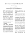
Design Techniques to Implement Reconfigurable
Hardware Watch-Points for Hardware/Software
Co-Debugging
Karen A. Tomko and Anurag Tiwari
{ktomko, atiwari}@ececs.uc.edu
Department of Electrical and Computer Engineering and Computer Science
University of Cincinnati, Cincinnati, OH 45221-0030
Abstract- Application Development for FPGA
based reconfigurable systems includes hardware
design, for circuitry to be mapped on FPGAs, and
software design for a general-purpose processor. A
significant part of the application development for
reconfigurable systems is debugging and validation
of
the
hardware
and
software
design.
Hardware/software co-debugging and development
of techniques for reducing the hardware debugging
time is an important issue. This paper describes how
reconfigurable hardware watch-points in the FPGA
designs can be used in a hardware/software
debugging environment and can expedite the
hardware debugging. We have described the
techniques to add watch-point logic at many different
steps in the FPGA design flow. We also discuss how
these techniques can be automated, and how new
debugging tools such as Jbits and Jroute can be used
to modify the watch-point logic and further reduce
the hardware debugging time. Using one of the
proposed techniques it is observed that watch-point
logic modification has a speedup ranging from 5 to
12 times for different benchmark circuits.
1 Introduction
A typical reconfigurable computing application
consists of hardware running on one or more FPGA
devices present on a co-processor board and software
running on the general-purpose processor. Debugging
of these applications involves debugging of both the
hardware and software components. Hardware
simulation is one of the most widely used techniques
for hardware debugging and validation before design
implementation. Hardware simulation allows the
designer to examine the circuit in detail, but can be
prohibitively slow. It can take hours to days for the
designer to reach a desired point of interest. This
process of debugging can be very time consuming at
initial stages of the design, when multiple simulation
runs may be required to correct an error. Thus,
isolated debugging of hardware and software
components using simulators can be a time
consuming process. Besides, the final application
after integration may still not work because of the
errors induced after integration of these two
components.
The problem of lengthy hardware debugging time can
be mitigated by running the hardware directly on the
target platform; Since, for reconfigurable computing
applications the target platform is available before the
design is completed. There has been some research
done in the area of debugging for reconfigurable
computing using the target platform [1][2][3]. The
key feature behind these debugging efforts is the use
of the readback capability provided in some of the
FPGAs [4][5][6]. A readback operation can acquire
internal state of FPGA internal elements such as the
LUTs, flip-flop and IOBs and can match that
acquired state with the symbolic name in the original
design. Thus, the user can use readback to analyze
the values of the signals during execution. The
readback operation can be used to get the circuit state
at any point during the design execution. The clock
supplied to the design is halted before the readback
operation is initiated. Once the clock is suspended,
the signal values can be sampled out by stepping the
clock one by one (single-stepping) or after stepping
many clock cycles at once (multi-stepping). The
readback capability while allowing the designer to
debug the design on the target platform has a few
drawbacks. For example, the designer cannot initiate
the readback operation without stopping the design
execution or halting the clock. Another problem with
design readback is that it is a slow operation;
Configuration readback of the complete design takes
around 1 second, which makes it too slow to check a
signal value every clock cycle.
To overcome the slow speed of the readback
operation, an additional debugging circuit can be
added into the design. The added debugging circuit
(watch-point)
provides
the
designer
with
observability and controllability, while the design
executes at or close to normal speed. The design
running in the FPGA can be executed until the user
desired point without stopping in between. Then the
readback operation can be initiated to observe and
analyze the circuit status. The additional debugging
circuit is removed from the design, when the whole
debugging and validation process is completed. Thus,
final design after validation process has the same area
and speed as the design before adding debugging
circuit. The hardware watch-points enable a
controlled execution of the hardware design and
speed up the debugging procedure by minimizing the
user intervention in debugging.
One of the most obvious ways of adding debugging
logic in the design would be to add it before the
design is synthesized. The debugging logic can be
added in HDL, schematic entry or in its netlist.
However, if the debugging logic is added in the top
most level in the design flow, any modification in
that logic will entail a complete recompilation of the
design, which is a time consuming process and can
take up to a few hours for big designs. Many
debugging logic modification iterations may be
required if the designed being debugged is at an
initial stage of development. However, the large
recompilation time can make this complete
debugging process very slow.
In this paper, we have proposed different techniques
to add debugging logic into the design. The use of
Jbits and Jroute to further reduce the modification
time of debugging logic by altering the configuration
bit file is also discussed.
2
Related Work
The addition of debugging logic in FPGA designs for
debugging and validation purposes has also been
proposed by other researchers [7][8]. For example, in
[7] a design level scan chain is proposed for complete
design debugging. However, area overhead of this
design chain can reach up to 100%, which may
restrict this technique to less congested designs. In
[8], a technique to modify debugging logic is
proposed using a java based design environment.
This technique limits designers to a java based
structural design environment, which is less familiar
than a behavioral HDL/Schematic environment. The
technique proposed in [8] allows instrumenting the
debugging logic at bit-level, but in some cases the
modification can be quite frequent, and thus time to
make the new bitstream and time to load the
bitstream on target FPGA may make the debugging
process slow.
Many commercial tools provide more automated and
powerful features to add and modify the debugging
logic in the design. Xilinx has a tool named
Chipscope[9], which allows the designers to put
embedded logic analyzer(ELA) cores in their designs.
These ELA can monitor design signals during design
execution and can produce a trigger if the signals
meet some predefined condition. The trigger
conditions and signals monitored can be changed
without any design recompilation. Chipscope needs a
logic analyzer to view the signal status and a port on
the reconfigurable computing board to connect it. In
addition, the area overhead of ELA is fixed, i.e. even
if designer needs only few signals to be monitored,
the area overhead will be the same. Altera also has a
product named SignalTap[10][11], which is a logic
analyzer embedded into the design running on the
FPGA. SignalTap is similar to Chipscope in
operation, however any modification in the
debugging logic except for changing the trigger
condition requires complete recompilation of the
design.
Validation and debugging of the design by adding
debugging logic is not limited to FPGAs. For
example, Triscend E5 configurable system on chip
platform [12] has on-chip debugging support using an
additional breakpoint logic unit kept on the chip. This
breakpoint unit monitors the user specified
combinations of address and data control. The MCU
freezes at the end of the current condition, whenever
a breakpoint condition occurs. The breakpoint unit,
though aids the user in debugging is limited only to
the data, control and DMA signals. SIDSA also has a
system on chip known as FIPSOC [13], which also
has the hardware breakpoint capability [14]. The
breakpoint mechanism in FIPSOC is similar to that in
Triscend E5, i.e. breakpoint can be set only on user
specified data and address values.
In [3], a software watch-point facility is presented. In
this technique, the comparison between user specified
condition and actual value design signals is
performed in the software running on general purpose
processor. This operation of comparing FPGA design
signals in software entails readback of the design
signals at every clock cycle (single-stepping) or after
every fixed number of clock cycles (multi-stepping).
Single stepping the clock makes the whole debugging
procedure very slow, as each readback operation
takes around 1 second with software overheads. On
the other hand multi-stepping the clock can
completely miss a user-desired event.
3
Reconfigurable Hardware Watchpoints
Just as in software debugging tools and hardware
simulators, watch-points can be introduced in
hardware designs running on the FPGAs present on a
co-processor board. These watch-points can monitor
signal(s) for any user specified event or condition.
The user can specify the signal(s) present in the
design to be monitored for a particular value and/or
an event. Table 1 shows the trigger conditions for
which a signal can be monitored. The signals, which
are monitored, are compared with the user-defined
pattern or an event, and this operation takes place
every clock cycle. If there is a match, between the
signal value and the user specified trigger condition,
the design running on the FPGA stops executing and
an interrupt is given to the application program
running on a general-purpose processor. Upon getting
an interrupt from the FPGA co-processor board the
software running on the general-purpose computer
may initiate a readback operation to obtain the
internal state of the circuit. The hardware execution
cessation is achieved by disconnecting the processing
element clock from the FPGA design. To provide the
similar watch-point capability as software debugging
tools, the design should be able to restart from the
same point after the watch-point condition is reached.
This requires control over the system clock, which
should be disconnected from the design whenever the
user specified condition occurs, and should be
connected back to design after the readback
operation. This clock control is implemented with
some simple Finite State Machines (FSMs) and a
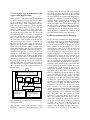
gated clock. An FSM takes input from all the signals
monitored for a particular condition/event and when
the desired condition is reached the FSM outputs an
interrupt. This control FSM gives input to another
FSM, which controls when to enable or disable the
clock. Once the interrupt has been acknowledged by
the
Control
FSM
User defined
logic and
watch-point
conditions/
events
Interrupt
Clock
In
Clock gating
FSM
Clock Out
Fig.1. Diagram of clock control operation
Software running on the general-purpose computer
the control FSM can enable the clock. This operation
is illustrated in figure 1. Any signal can be set to a
variety of trigger conditions, also if there are multiple
trigger conditions for a signal they can be logically
ANDed or Ored depending upon the requirement.
Similarly, if there are multiple signals with different
trigger conditions, they can be ANDed or Ored to
make one interrupt output. Table 1 shows the trigger
conditions implemented. The trigger conditions
mentioned in table 1 provide the user with flexibility
in debugging. Any of these conditions can be set such
that they should be asserted for some user defined
number of clock cycles. This includes two situations,
one in which the condition is satisfied for consecutive
clock cycles and a second in which the condition
must be satisfied for some number of user defined
clock cycles (not necessarily in a row).
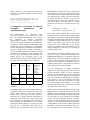
Trigger
Condition
Greater than
Greater
equal to
Description
than
Less than
Less than equal
Not equal to
Equal to
Rising
only
edge
Falling
only
edge
Both
edges
(rising edge or
falling edge)
Trigger when signal monitored is
greater than watch-point value
Trigger when signal monitored is
greater than or equal to watch-point
value
Trigger when signal monitored is
less than watch-point value
Trigger when signal monitored is
less than or equal to watch-point
value
Trigger only when the signal
monitored value is not equal to
watch-point value
Trigger only when the signal
monitored value is equal to watchpoint value
Trigger only when a signal
monitored makes rising edge
transition
Trigger only when a signal
monitored makes falling edge
transition
Trigger when a signal monitored
either makes falling or rising edge
transition
Table.1. Watch-point trigger conditions.
4 Watch-point logic implementation
Three techniques are described for watch-point logic
implementation in this paper. These are discussed in
the following sections.
4.1 Addition of watch-point constant in HDL
(Hardwired condition)
The first technique of adding debugging logic is the
addition of watch-point signals with constant value.
These constant type signals have the same type as of
the signals that are being monitored in the HDL
design. The constant signal value is the value, which
the watch control logic compares with the monitored
signal. In this method the trigger condition for user
selected signals is designed and added in the HDL.
The modified HDL is then synthesized to implement
and optimize the design with debugging logic. Of all
the three techniques discussed in this paper, this
implementation gives the most area optimized
solution for adding the watch-point logic. This
technique is well suited for the designs, which have a
high area or CLB utilization, and have little room for
additional logic. However, any change in the watchpoint logic pattern or condition has to be made in the
HDL file itself. This is because after synthesis
optimization, placement and routing of FPGA design
many signals names are changed; Thus, it is difficult
to relate the watch-point constant signals with the
signals name generated after synthesis, placement
and routing. This procedure of changing watch-point
logic can be time consuming for large designs,
because each iteration of watch-point logic
modification will require the whole of synthesis and
place and route time.
4.2 Implementation of watch-point logic by
instantiating library primitives (Component
instantiation)
The watch point logic can also be implemented by
instantiating library primitives which can be
technology-specific or technology independent. In
this research, we have used Xilinx FPGA and so its
library primitives such as flip-flops, latches, LUT
RAMs and LUTs (use of LUT instantiation in HDL is
available in Virtex series only). The user has to
manually synthesize the logic when implementing
watch point logic using library primitives. For
example for constructing an eight-bit register, the
user has to connect eight instantiated flip-flops in the
VHDL design. Similarly, for mapping any function
into Lookup Table (LUT) RAM, LUT ROM or LUT
primitive the user has to program them appropriately.
This can be done using logical constraints inserted
into the HDL design and/or in the constraint file at
the time of place and route. If flip-flops are used to
implement the watch-points then a flip-flop is
instantiated for storing every single watch-point logic
bit in the design. The values of these flip-flops are
then compared with the monitored signal using a
comparator, which generates an interrupt on match.
For example, if there are a total of 32 bits of watchpoint logic (e.g. for monitoring a 32 bit wide signal)
in the design, then 32 flip-flops have to be
instantiated and are set or reset based on the watchpoint pattern. It has been observed that when design
primitives are used in the design, the signal names
associated with them are preserved even after
synthesis, place and route. Thus, values stored in the
flip-flop can be changed in the final binary file,
which is generated after place and route, by
identifying the respective watch-point signals. To
change the value of these flip-flops the user must
know where these components are placed in the
FPGA. This information can be obtained from
parsing the user accessible text file, containing
information about placement of all the components in
the design. In Xilinx design flow this text file is
generated by converting a Native Circuit Description
(.NCD) file into text file. Once the user has
ascertained the exact location of flip-flops, a script
file is written for the Xilinx FPGA Editor [15] to
automate the changes in the NCD file. The changing
of the watch-point value is fast and efficient in this
way, as the user just has to change values in the script
file each time a change in the watch-point values is
required and then generate a new bitstream from
modified NCD file.
Watch-point logic can also be implemented using the
LUT RAM/ROM instantiation. For example, for
implementing a “greater than” condition, the signal to
be monitored is connected on the address lines of a
LUT. The LUT is then programmed with logical one
for an active high interrupt signal at all the locations
greater than the given value and logical zero every
where else and vise versa for an active low signal.
Similarly for implementing the comparison “less
than” the LUT is programmed with a logical one for
an active high interrupt signal at all the locations less
than the given value and logical zero every where
else and vice versa for an active low signal.
For detecting the rising and falling edges, library D
flip-flops are instantiated and they are clocked with
the monitored signal. For rising-edge, a non-inverted
connection is made to the CLK pin and for fallingedge an inverting connection is made to the clock
input of the flip flop. The interrupt acknowledge
signal is connected to the reset or preset input of the
flip-flops to clear the interrupt once it is
acknowledged. The last condition, where the signal
must satisfy the condition for a given number of
clock cycles, is implemented by keeping a counter in
the design.
4.3 Watch-point logic implementation using
register chain (Register chain)
In this approach, watch-point logic is implemented
by storing a watch-point signal value in the flip-flops.
In this technique, a design level register chain is
added in the design, which is analogous to flip-flop
scan chain in VLSI testing [16]. All the flip-flops
required for implementing watch point logic are
connected together to form a register chain. The
register chain is formed by connecting output of one
flip-flop to the input of other and so on. At the time
of initialization, data corresponding to watch-point
values are shifted into the respective registers. It
takes as many clock cycles to shift the data as there
are watch-point values registers in the design. The
data coming out of these registers is compared with
the user specified signal using a comparator.
Whenever the user wants to change the watch point
signal pattern, the RESET signal is asserted in the
design and appropriate data is given at the memory
input port. A control FSM is added into the design to
synchronize the operation of shifting the data and
enabling the reset logic. Upon receiving RESET
signal the controller starts shifting the data serially
across the register chain. The advantage of this
methodology of register chain is that user can change
the watch point signal on-line by just asserting the
RESET signal, which can be asserted using software
API calls. Moreover, the time consuming synthesis,
place and route process is bypassed completely in
this technique.
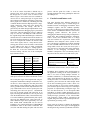
Temporary holding register
D
Q
CLK
D
Q
CLK
Comparator
CLK Out
Control logic for
shifting the data
into flip-flops
D
Q
CLK
Interrupt
Signals to be
monitored
USER Defined logic
Running inside the
FPGA
Fig.2. Block diagram showing watch-point technique
using register chain
This technique can be easily integrated with an
interactive GUI-based hardware/software co-
debugging utility, developed as part of this research.
The reason for quick integration of this technique
with co-debugging is that the user only has to provide
the values stored by the register chain using the GUI;
No partial or complete recompilation of design is
necessary. Figure 2 illustrates this methodology. This
technique, while allowing the user to change the
watch-point signal values on-line, does not allow online change in the watch-point conditions. To change
a watch-point condition, which is implemented in a
comparator, the user can change the LUT values of
the LUTs which corresponds to the comparator in the
NCD file and then generate a new bit-stream.
4.4 Bitstream Modification for Debugging
In all of the above techniques for adding debugging
logic in the design, the user cannot change the signals
connecting to the debugging logic without complete
or partial recompilation of the design. The signals,
which connect to the debugging logic, can be
changed at the netlist level or after the place and
route (PAR) process. Changing of signals connected
to the debugging logic requires two steps. First, the
original signal has to be disconnected from the
debugging logic; second, the new signal has to be
connected to the debugging logic. If the signals
connectivity has to be changed at the netlist level, the
user has to identify the original and the new signal in
the netlist and update the netlist for new connectivity;
and finally do the place and route of the netlist. This
process of updating the netlist and PAR can be time
consuming. The signal connectivity can also be
changed after the PAR, by opening the Native Circuit
Description (.NCD) file in Xilinx FPGA editor [15].
However, identifying and manual routing of signal
source and sink can also be a time consuming
procedure. To mitigate this problem we have
proposed the use of Jbits and Jroute[19] from Xilinx,
to change the signal connectivity at configuration
bitstream level. The JBits tool suite is a set of Java
API to build, test, debug and modify design at the
configuration bitstream level. At this level, Jbits
gives read and write access to all configurable
elements and access to all the routing resources of the
FPGA. Modification in the design for changing
signal connectivity can be performed in few seconds
using the JBits API. The change in signal
connectivity is done using JRoute, which is a part of
JBits. For changing signal connectivity, first the
signal source and sink are identified. This operation
can be done using the map report file(.mrp) generated
by Xilinx place and route. Then the original net
connected to the source is unrouted using the
respective API call. Finally, the API call to route a
net between source and sink is used, to make new
signal connectivity. Source and sink are the pins
attached to a CLB. This operation is elaborate in the
excerpt below.
Pin_Source=(CLB_Row_20,CLB_Column_12,Out_S0_XQ)
Pin_Sink = (CLB_Row_17,CLB_Column_9, Input_S1_F1)
jroute.unroute(Pin_Source);
jroute.route(Pin_Source, Pin_Sink);
5 Comparison and analysis of different
techniques
implemented
and
experimental results
The
methodologies
for
watch-point
logic
introduction, discussed in the sections above have
their own advantage and limitations. Table 2 shows
the
comparison
of
different
watch-point
implementation techniques. These techniques are
evaluated for the area overhead, ease of modification,
time taken to modify watch-point signal patterns and
whether they can be modified by a co-debugging
interface developed between hardware and software.
Since the original design is already constrained (at
the time of synthesis and place & route) for the speed
requirements, the addition of watch point logic does
not slow down the design. In the placement and
routing process, the watch-point logic is not
constrained so the placer has the flexibility to place it
anywhere to meet the original design constraints.
Watch-Point
technique
Area
Overhead
Time to
change
watchpoint
value
Large
Small
Changes in
watch-point
values
possible
through codebug
interface
YES
Medium
Medium
NO
Small
Large
NO
FSM. Equations (1) and (2) below show an increment
in the CLB count by the register chain and the control
FSM respectively. It is assumed that N is the number
of watch-point logic condition value bits required in
the design and thus the number of clock cycles
required to shift the data. In our experiments we have
used Xilinx FPGAs and each CLB in a Xilinx
XC4000 and Virtex series of FPGAs has two flipflops.
Count(CLBs) = ceil(N/2)
(1)
Count(CLBs) = (ceil(log2N)+1)/2 (2)
The register chain technique also requires more
routing resources to connect all the watch-point flipflops together, which may be scattered all throughout
the FPGA. Instantiating flip-flops has the same area
overhead for keeping watch-point value as in register
chain i.e. one flip-flop per bit but in this case the
control FSM is not needed and also less routing
resources are used. However, in this method, a part of
design recompilation is necessary for any change in
watch-point logic values.
If the number of watch-point condition bits is large
and area is a major concern then instantiating LUT
RAM/ROM methodology is an optimum solution. In
Xilinx FPGAs a LUT has four address lines therefore
a four bit wide watch-point can be programmed in a
single LUT. If the signal to be monitored is a bus, it
is broken down in four bit wide signals for each LUT
output, which are later ANDed together.
Table.2. Comparison of different watch-points
techniques
The first methodology of making watch-point
changes in the HDL design itself is the most area
efficient technique among all three techniques
discussed. In this methodology synthesis, place and
route has full freedom to optimize the watch-point
logic thus an optimized implementation is obtained.
If the design is very big and densely routed this
methodology may still make introduction of watchpoint logic possible, other techniques on the other
hand may fail because they consume more area and
may require more space to route.
If the design under test is a stable design without the
possibility of many errors and there are only a few
signals, which require a watch point, keeping a
register chain in the design is the best option as it
allows the user to quickly make the modification in
watch-point patterns and can be easily incorporated
into an interactive co-debugging utility. The register
chain technique has the maximum area overhead
among all the three techniques, as it requires one flipflop per bit of watch-point value and has an
additional area overhead for the logic of the control
We have used six different benchmark circuits for the
implementation of different watch-point insertion
techniques. These benchmark circuits are part of the
High Level Synthesis (HLSW 92), PREP benchmark
suite, and some are freely available processor VHDL
models. The largest benchmark circuit is a SPARCS
complaint processor obtained from European Space
Agency [17]. The target FPGA for these experiments
is Xilinx 4085xl; Leon processor, which is the largest
benchmark, could not fit into XC4085xl and so we
have used Xilinx Virtex series of FPGA ‘XCV300’
Register
chain.
Component
instantiation.
Hardwired
condition
for it. In its current form, JBits is limited only to
support Virtex series of devices. Thus, we mapped
the designs also to Virtex series of FPGA to use
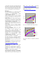
JRoute. Figure 3 and 4 shows the area overhead for
various sizes of watch-point logic for register chain
and component instantiation techniques respectively.
These graphs were obtained by calculating the CLB
overhead obtained from the Map Report File (.mrp),
which contains the CLB count of the design after
mapping, placement and routing. This file is
generated by the Xilinx design implementation tools.
The circuit without the debugging logic is placed and
routed first. Then the debugging circuit is added in
steps of a few bits, and finally the CLB count from
the original design and modified design is obtained to
calculate the area overhead. Each time the number of
bits of the monitored signals is increased, the design
has to be recompiled to calculate the accurate CLB
count. In the figures, there is a steep increase at the
starting point because of the fact that a control FSM
is also added at the time of initial watch-point
addition. For the first technique i.e. adding signals to
the HDL file, it has been found that CLB count
increases linearly with the size of the watch-point
logic (number of bits).
Benchmark Circuit
Normal
Guide mode
Place and
place and
route time route time
(minutes)
(minutes)
Leon Processor
25.13
2.18
6502 microcontroller
5.50
1.26
AM2901
1.9
0.37
PREP5
2.51
1.1
PREP4
1.7
0.53
HC11
8.53
1.38
Table 3: Comparison between normal and guided
mode place and route for different benchmark circuits
The watch-point logic when implemented using the
component instantiation technique mentioned in 4.2,
can have its values changed in the final placed and
routed design, using guided place and route (PAR)
facility provided in the Xilinx implementation tools
[18]. Guided PAR can be used to speed up the time
consuming place and route process. Guided PAR
tool, take an already placed and routed file as an
input, and using this information it tries to place and
route the modified netlist. Thus, if the netlist has only
a few minor additions, guided PAR only has to place
and route the additional logic. Place and route of
small additional logic takes significantly less time
than normal PAR. Guided PAR can be used in
technique 4.2 by putting a different LUT RAM/ROM
initialization value in the Netlist Constraints File
(.ncf) file and then running the place and route and
process with the guide file. Table 3, shows the
speedup obtained when using guided place and route
for technique 4.2
6
Conclusion and future work
This paper describes three different approaches to
introduce watch-points logic in FPGA design for
hardware/software co-debugging environment. These
techniques together with the readback capability
provide a co-debugging environment which has most
of the features of traditional hardware and software
debugging systems. Moreover, this process of
debugging the hardware design using watch-points is
much faster than traditional hardware simulation.
Table 4 shows some simulation times of a design
with and without the co-processor board model
(Wildforce from Annapolis micro systems in this
case). The design is simulated at a Pentium 600 Mhz
PC with 512 MB of RAM. If there is an error in the
design which occurs after 4,194,303 clock cycles a
user may have to wait hours when using simulation.
Whereas, in the debugging environment using
hardware watch-points a user can instantly reach to
the point of interest (at the 4,194,303th clock cycle).
Type of Simulation
Run Time
Minutes (hours)
Functional
40.5 (.675)
Functional with board model
516 (8.6)
Timing level
46.5 (.775)
Table 4: ModelSim simulation times for a
synchronous counter run for 4,194,303 clock cycles.
In addition, these techniques allow the debugging of
the application running on the actual platforms, so
there is no need of doing multiple iterations of
hardware simulations (i.e. functional and timing with
delays back annotated in the design). To modify a
watch-point value or its condition a user may have to
synthesize, place and route the whole design which
can be time consuming process. Table 3 shows 5 to
12 times speedup we get over the normal synthesis,
place and route process when using one of techniques
proposed for implementing watch-point logic. We
have also discussed how we can incorporate JBits
and JRoute to further expedite debugging. Our ongoing research focuses on the complete automation of
watch-point logic generation; i.e. the relevant HDL
code generation, which could be inserted into the
original, design and which is generated upon the user
specification given using a GUI.
Future work can be done to enhance the debugging
techniques discussed in this paper for debugging of
the designs having external asynchronous interfaces.
A trace buffer can be kept in the design which will
keep history of the data coming through external
interface. With the help of data in the trace buffer a
user can ascertain the inputs (coming from external
interface) which might have caused a malfunction.
IEEE
press
1990
ISBN
0-7803-1062-4
[17]http://www.estec.esa.nl/wsmwww/leon/
[18] Using Xilinx and Synplify for Incremental
Designs (ECO), Xilinx application note XAPP164,
Xilinx San Jose, CA 1994
[19] http://www.xilinx.com/products/jbits/
Reference:
250
CLB overhead
200
150
100
6502
2901
hc11
50
prep4
prep5
Leon
0
0
50
100
150
size of watch-point logic (# of bits)
Fig.3. Area overhead for register chain technique
50
45
40
35
CLB Overhead
[1] B.L. Hutchings et. al. A CAD suite for high
performance FPGA design, proceedings of IEEE
Symposium on Field-Programmable Custom
Computing Machines, April 1999
[2] B.L. Hutchings and Brent E. Nelson. Unifying
Simulation and Execution in a Design enivornment
for FPGA Systems IEEE trans on VLSI Vol 9 No 1,
February 2000
[3] K. A. Tomko and A. Tiwari. Hardware/Software
Co-debugging for Reconfigurable Computing IEEE
International High Level Design Validation and Test
workshop, Oakland CA, November 2000
[4] Virtex FPGA series configuration and readback.
Application Note XAPP138, Xilinx San Jose CA,
October 2000
[5] W. Holfich. Using the XC4000 Readback
Capability, Xilinx application note XAPP015, Xilinx,
San Jose, CA 1994
[6] Lucent Technologies, Allentown, PA, ORCA
Series 4 FPGAs, Dec 2000
[7] T. Wheeler et. al. Using design-level scan to
improve
FPGA
design
observability
and
controllability for functional verification FPL’01
[8] Paul Graham et. al. Instrumenting Bitstreams for
Debugging FPGA Circuits proceedings of IEEE
Symposium on Field-Programmable Custom
Computing Machines, April 2001
[9] Xilinx, San Jose CA. ChipScope software and
ILA Cores User Manual, v. 1.1. June 2000
[10] Altera, San Jose CA. SignalTap Embedded
Logic Analyzer Megafunction, April 2001 ver.2.0
[11] Altera Inc, San Jose CA. Quartus II SOPC
Design Software.
http://www.altera.com/products/software/quartus2/qt
s-signaltap.html
[12] Triscend Inc. E5 Configurable System-on-Chip
Platform data sheet, July 2001 (ver. 1.06)
www.triscend.com/products/dse5csoc.pdf
[13] SIDSA Inc, SF CA, FIPSOCTM Mixed Signal
System-on- Chip.
http://www.sidsa.com/FIPSOC/Fipsoc%201.2.html
[14]FIPSOC user manual chapter 7, SIDSA Inc.
http://www.sidsa.com/FIPSOC/Users_manual/Chapte
r_07.pdf
[15]Xilinx Inc, Xilinx 4 Software Manuals.
http://support.xilinx.com/support/sw_manuals/xilinx4
[16] M. Abramovici, M.A. Breuer, A.D. Friedman.
Digital Systems testing and testable design pp. 358
30
25
6502
2901
hc11
prep4
prep5
Leon
20
15
10
5
0
0
50
100
150
size of watch-point logic (# of bits)
Fig.4. Area overhead for Component instantiation
technique