1
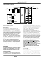
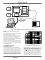
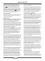
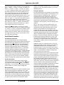
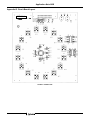
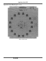
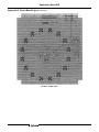
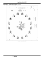
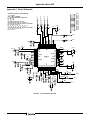
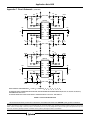
HA456EVAL1 Evaluation Board User’s Manual
Application Note
October 1999
AN9856
Description
Features
The HA456EVAL1 evaluation platform provides a quick and
easy method for evaluating the HA456 (AV = 1) 8 x 8 video
crosspoint switch in the 44 Lead MQFP package. The
HA456CN is included with the evaluation board.
• Emulates a Complete 8 x 8 Video Switcher
The evaluation platform includes the populated PCB, a
floppy disk containing software for programming the HA456
state from a PC, and product data sheets.
• Optional Adaptor (HA456/7EVAL3) Allows Simple Manual
Control of Channel Selection (No PC Required)
Operation and channel selection is easily accomplished by
using a PC and parallel printer cable along with the included
software. Alternatively, manual control is possible using the
optional HA456/7EVAL3 board which contains the
necessary switches to drive the control and data inputs, and
connects directly to the HA456EVAL1 36 pin connector.
To evaluate the HA457 (AV = 2) 8 x 8 video crosspoint
switch, please refer to the HA457EVAL1 documentation.
• Simple and Easy to Use
• PC Controlled (Software Included) Channel Selection
• Configurable for Buffered (HFA1412) or Unbuffered
Outputs
• Configured for 75Ω Environments
Applications
• Video Switchers and Routers
• Security Systems
• Video Conferencing
Ordering Information
PART
NUMBER
HA456EVAL1
DESCRIPTION
Evaluation Platform for
8 x 8 Crosspoint Switch
1
PACKAGE
SUPPORTED
44 Ld MQFP
CAUTION: These devices are sensitive to electrostatic discharge; follow proper IC Handling Procedures.
1-888-INTERSIL or 321-724-7143 | Copyright © Intersil Corporation 1999
Application Note 9856
Functional Block Diagram
HA456
HFA1412IP (OR HFA1405IP)
AV = +2
VIDEO
IN
(1 OF 8)
75Ω
75Ω
VIDEO
OUT
(1 OF 8)
INPUT
BUFFERS
WR
LATCH
CE
PROGRAMMING
CONTROL
8X8
SWITCH
MATRIX
A2
A1
A0
OUTPUT
SELECT
INPUT
SELECT AND
COMMAND
CODES OR
SERIAL I/O
D3
D2
D1/SER OUT
D0/SER IN
AV = +2
36 PIN CONNECTOR
Functional Description
Block Diagram
The Functional Block Diagram illustrates the major
components of the evaluation board. The centerpiece of
the board is the HA456, AV = 1, 8 x 8 video crosspoint IC
which is comprised of 8 low capacitance input buffers (thus
requiring no external input buffer ICs), a 64 element switch
matrix, and unity gain output buffers. Also on the board are
two HFA1412 quad programmable gain (±1, +2) buffers
ideally suited for driving video cables and other low
impedance loads. Note that the HFA1412s are configured
for a gain of 2, thereby setting the overall gain on the eval
board at unity if each output is terminated with a shunt 75Ω
resistor.
The 36 pin connector interfaces the board with a PC
through a standard “Centronics compatible” printer cable.
Through this connector the PC controls the programming
control, address, and data lines (see Appendix A for the
connector pinout). The evaluation board may be evaluated
using the parallel or serial interface mode, and edge or
level LATCH control.
Performance
The HA456 combined with the HFA1412 delivers 100MHz
bandwidth with 0.03% differential gain and 0.05 degree
differential phase when driving a standard 1VP-P video
signal into a single video load.
Platform Description
The HA456EVAL1 is a four layer board comprised of two
signal layers, a power layer, and a GND layer (see Figures
2
4-7). The board can accommodate BNC or SMA connectors
on the 8 inputs and 8 outputs. Provisions are made for shunt
terminations on the inputs and series terminations at the
outputs. Input and output signal traces are guarded to
minimize adjacent channel crosstalk.
For easy programming of the HA456 switch state, the
platform includes a 36 pin “Centronics” type connector which
connects to a PC’s parallel port via a printer cable (not
included). The included software allows the PC to interface
with the HA456 via serial or parallel programming schemes.
The platform includes test points to monitor the output states
(at the connector) and the digital control line states. Series
1kΩ resistors isolate the control line test points from the
Centronics connector, to prevent inadvertent short circuits
from damaging the PC’s parallel port drivers.
Two position jumpers allow the user to select a serial or
parallel programming interface (S/P), select edge or level
LATCH control (E/L), and to enable or disable CE.
The platform includes test pins (essentially a high frequency
socket) for separate output buffer ICs to facilitate
experimentation with quad op amps and programmable
buffers.
Power connection is via three banana plugs, one each for
V+, V-, and GND.
Default Configuration
The evaluation board, as ordered, is configured (see Figures
8-9 for the schematic) with an HA456 crosspoint driving a
1kΩ load to GND (R19, R22, etc.), and a series resistor (0Ω
default) connected to the noninverting input of an HFA1412
Application Note 9856
quad, programmable gain buffer. The HFA1412 is configured
for a gain of 2 (R35, R38, etc. = 0Ω), and drives the output
connector through a 75Ω series termination resistor. Input
and output connectors are BNC type, with all 8 inputs
terminated by shunt 75Ω resistors.
PC Controlled Operation
Programming jumpers are set for Parallel programming
interface (S/P (JMP2) = GND), Level mode LATCH signal
(E/L (JMP1) = GND), and CE input jumpered high (JMP3 =
5V, i.e., chip enable controlled by the state of CE).
The evaluation platform includes Windows based (Windows
3.1 or newer) software for controlling channel selection and
state. The software provides control over the WR, LATCH,
CE, A2:0, and D3:0 control lines, and allows operation in
either serial or parallel programming modes. Simply connect
a “Centronics compatible” printer cable between the PC’s
parallel port and the eval board connector, fire up the
software, and follow the on-screen instructions.
Optional Configurations
Manual Operation (using HA456/7EVAL3 Adaptor)
The HA456 evaluation board features the flexibility to allow
the user to change the evaluation configuration. Some of the
more popular changes are discussed below.
If a PC isn’t available, or if the user likes to get his hands
dirty, the HA456 evaluation board can be manually controlled
using the optional HA456/7EVAL3 daughter card. This card
plugs into the HA456EVAL1 36 pin connector, and contains
switches to drive the control, data, and address lines. For
more information please see the HA456/7EVAL3 user’s
manual.
Replace HFA1412 programmable gain buffers with HFA1405
op amps (included with gain setting resistors in small, black
sample box). The Quads are installed in socket pins for easy
replacement while maintaining excellent high frequency
performance. Use the 402Ω resistors from the sample box
for the RF (R36, R37, etc.) and RG (R35, R38, etc.) of each
amplifier. Note that 0Ω resistors occupy the RG position in
the default configuration.
Add a series resistor between the HA456 and HFA1412 to
tune the output response - Replace the 0Ω series resistors
(R20, R23, etc.) between the HA456 outputs and the
HFA1412 inputs with the desired resistor value.
Serial mode digital interface - Connect the S/P jumper
(JMP2) to V+.
Edge mode LATCH signal - Connect the E/L jumper (JMP1)
to V+.
Drive output connectors directly from the HA456 - Remove
the HFA1412 ICs from the “sockets”. Add the desired value
series output resistors between the HA456 outputs and the
connectors (R21, R24, etc.). Note that the ICC measurement
now reflects only the HA456 supply current.
Replace BNC connectors with SMA connectors - The eval
board accepts PC mount SMA straight jack type connectors
(e.g., Johnson Components part #142-0701-211). Simply
unsolder the BNC connectors, and solder the SMA
connectors in the appropriate holes.
Power Supplies and Ground
The HA456EVAL1 operates on ±5V supplies which must be
capable of supplying at least 250mA. Connect the red
banana plug to +5V, the black plug to -5V, and the green plug
to GND. The evaluation board contains only one connection
for each power supply polarity, so the measured ICC
includes contributions from the two HFA1412s when they are
installed in their sockets. A solid GND plane is a must for
maximum AC performance and to minimize crosstalk. The
HA456EVAL1 devotes a whole layer to the task. Note that
each input and output line is surrounded by AC GNDs to
minimize coupling.
3
Getting Started
Required Materials List
To ensure that everything on the board is configured
properly and is functional, it is suggested that the following
test be performed. The board test requires:
1. HA456EVAL1 Evaluation Board.
2. Power supplies for ±5V capable of delivering 250mA.
3. Personal computer with a parallel port.
4. “Centronics compatible” printer cable.
5. Two 75Ω BNC cables.
6. A network analyzer (or measurement tool of choice).
Set Up Instructions (Refer to Figure 1)
Ensure that the jumpers are set for parallel mode interface
(S/P (JMP2) = GND), Level mode LATCH signal (E/L (JMP1)
= GND), and CE active (JMP3 = V+). Execute file
EVAL456.exe from the floppy enclosed with the eval board.
Firing up the software first ensures that the computer’s
parallel port is driving all zeros. Connect the printer cable
between the PC and the eval board. Connecting the cable
after applying power to the HA456 may cause glitches which
can write erroneous data into the HA456 control registers.
Attach ±5V power supplies to the evaluation board, +5V to
the red banana plug, -5V to the black plug, GND to the green
plug, and power them on. Note that at power up, the state of
the HA456, with parallel mode selected, is input 0 connected
to all outputs, but with all outputs disabled, thus the
HFA1412 outputs will sit at GND (HFA1412 inputs pulled low
by 8 x 8 1kΩ load resistors). The evaluation board ICC
should read about 90mA with the HA456 outputs disabled.
Connect a 75Ω BNC cable from the network analyzer source
(RF Out) to the IN0 connector on the eval board. Set the
source level so the network analyzer delivers 1VP-P into the
75Ω input termination. Connect another similar cable from
Application Note 9856
HA456EVAL1
EVALUATION BOARD
+5V
POWER
SUPPLY
HA456CN (INCLUDED)
8
8 x 8 CROSSPOINT IC
8
-5V
POWER
SUPPLY
TWO
HFA1412IP
(INSTALLED)
OR
HFA1405IP
(INCLUDED)
QUAD BUFFERS
8
SELECTED
OUTPUT
OUTPUT
BUFFERS
PC INTERFACE
ANALOG
INPUT
75Ω
BNC
CABLES
SOFTWARE
INCLUDED
WITH
HA456EVAL1
PRINTER CABLE WITH
A 36 PIN “CENTRONICS”
TYPE CONNECTOR
(NOT INCLUDED)
NETWORK ANALYZER
PERSONAL COMPUTER
FIGURE 1. INTERSIL HA456EVAL1 EVALUATION SYSTEM SETUP BLOCK DIAGRAM
the OUT0 connector to the network analyzer receiver
(A or B).
RL =150Ω
RS =0Ω
Enable all outputs by typing “14” followed by “Enter”. The
signal at IN0 now connects to all outputs. Supply current
should increase to >110mA (current fluctuates due to
network analyzer sweep), and a unity gain transfer response
should appear on the network analyzer.
The network analyzer should display a response similar to
that shown in Figure 2. If it does, move the cable from output
connector to output connector to verify that all eight outputs
are enabled and functional.
Parallel Mode Evaluation
Parallel Mode Introduction
In the parallel programming mode, the Master Register
functions as eight 4-bit, parallel load, output control registers
which are accessed individually. The data in an output
register defines which input is currently associated with that
output. The state of any output is defined by writing a 7-bit
word to the HA456. Bits A2:0 select the appropriate output
register (if required), while bits D3:0 define the action for the
selected output. Outputs may be individually or collectively
4
GAIN (dB)
On the computer, type “1”, then “Enter” to select the parallel
interface with level mode LATCH signal.
VOUT = 0.5VP-P
3
0
-3
VOUT = 1VP-P
-6
1
10
FREQUENCY (MHz)
100
200
FIGURE 2. HA456EVAL1 FREQUENCY RESPONSE
enabled or disabled, or an output may be connected to any
input (codes 0-7), or to GND (code 8). If the action is a
channel switch (codes 0-8), the input code (bits D3:0) loads
into the Master Register on the rising edge of WR (assuming
CE and CE are both active). If the action is anything else,
D3:0 are immediately decoded (i.e., not loaded into the
Master Register) and the action occurs on the rising edge of
WR. Realize that this means that non-channel switch
operations occur asynchronously with regard to the LATCH
Application Note 9856
input; they are controlled solely by WR. Conversely, a
channel switch may be accomplished asynchronously, or
synchronously. For asynchronous switches, strap the
EDGE/LEVEL and LATCH pins low. With this setup, ALL
HA456 actions occur on the WR rising edge. Synchronous
operation is selected by driving the LATCH input from some
control logic, and strapping the EDGE/LEVEL pin high for
channel switching on the LATCH rising edge, or strapping it
low for switching whenever the LATCH level is low.
entries. The “Last action executed:” display confirms how the
last entries were interpreted.
After setting up the desired channel switch, toggle LATCH
low (code 16) to accomplish the switch. Remember: enable
and disable actions occur on the WR rising edge, without
regard for the LATCH state. Alternatively, control code 15
generates a software LATCH pulse, on the rising edge of
WR, which acts just like a hardware LATCH pulse.
Using the Software - Edge Mode
Set Up Instructions
Follow the procedure outlined under “Getting Started”. If the
board was previously powered up, power it off then on to
ensure a known starting state.
Basic Operation
At power up in parallel mode, the outputs are disabled, and
the eight 4-bit output registers are loaded with zeros (i.e., all
outputs are associated with IN0). Each output remains
disabled until it is enabled individually (code 12) or
collectively (code 14). Once enabled, an output immediately
passes the signal present at the input defined by the output
register contents (IN0 at power up), so it is possible to define
the input to output connections before enabling the outputs.
Using the Software - Level Mode
Ensure that the eval board E/L jumper (JMP1) is connected
to GND. Execute file EVAL456.exe from the floppy enclosed
with the eval board. Note that the program can be exited
from most screens by typing “E” followed by “Enter”,
however, the evaluation board should be powered off and
back on to ensure a known starting state whenever the
software is restarted.
Type “1”, then “Enter” to select the parallel interface with the
level sensitive LATCH signal. Note that the purple text at the
top of the screen indicates that the LATCH signal is low, thus
asynchronous channel switching is the default operation. For
synchronous, level mode operation, type “16” followed by
“Enter” to switch the LATCH signal high (no audible
confirmation of the action is given, but yellow text indicating
a LATCH high state replaces the purple text). Channel
switching will now occur only after the user drives the LATCH
signal low by typing “16" again (after which the purple text at
the top of the screen indicates that LATCH is in the low
state). Each subsequent entry of code 16 toggles the LATCH
state.
The program now prompts for an action control code (codes
11-16), or an input channel to associate with an output
channel. If this input requires specification of an output
channel (codes 0-8, 11, 12), the program prompts for it. After
each complete command (independent control code, or
input/control code and output combination), the program
generates a WR pulse, along with a visible and audible
indicator. Note: The program interprets alpha characters
(other than “E”) and most nonnumeric characters as a zero,
and treats them accordingly, but it rejects invalid numeric
5
Switch the eval board E/L jumper (JMP1) to V+. Execute file
EVAL456.exe from the floppy enclosed with the eval board.
Note that the program can be exited from most screens by
typing “E” followed by “Enter”, however, the evaluation board
should be powered off and back on to ensure a known
starting state whenever the software is restarted.
Type “2”, then “Enter” to select the parallel interface with the
rising edge sensitive LATCH signal. The purple text at the
top of the screen confirms that the LATCH signal is high. Use
control code 16 to generate a LATCH pulse (HI to LO to HI
transition) at any time a control code is requested.
The program now prompts for an action control code (codes
11-16), or an input channel to associate with an output
channel. If this input requires specification of an output
channel (codes 0-8, 11, 12), the program prompts for it. After
each complete command (independent control code, or
input/control code and output combination), the program
generates a WR pulse, along with a visible and audible
indicator. Note: The program interprets alpha characters
(other than “E”) and most nonnumeric characters as a zero,
and treats them accordingly, but it rejects invalid numeric
entries. The “Last action executed:” display confirms how the
last entries were interpreted.
After setting up the desired channel switch, pulse LATCH low
(code 16) to accomplish the switch. Remember: enable and
disable actions occur on the WR rising edge, without regard
for the LATCH state. Alternatively, control code 15 generates
a software LATCH pulse, on the rising edge of WR, which
acts just like a hardware LATCH pulse. Note that the
software LATCH command is a NOP if the LATCH input is
low when the command is written.
For a more thorough understanding of the LATCH input
functionality use the level mode section of the software (type
“1” after starting the program) with the HA456 strapped for
edge mode operation. This allows the user to set the LATCH
signal state, and explore the actions that occur on each
transition of WR or LATCH.
Parallel Mode Exercise
Follow the “Set Up Instructions” in the “Getting Started”
section, execute file EVAL456.exe, and power up the
evaluation board. Type “1” and “Enter” to select the
parallel/level mode evaluation segment. Toggle LATCH high
(code 16). Set up a channel switch for IN0 to outputs 0, 3,
Application Note 9856
6; IN 1 to outputs 1-2; IN2 to outputs 4-5, and ground OUT7
(type “1”, “Enter”, “1”, “Enter”, “1”, “Enter”, “2”, “Enter”, “2”,
“Enter”, “4”, “Enter”, “2”, “Enter”, “5”, “Enter”, “8”, “Enter”,
“7”, “Enter”). Enable all outputs (code 14). Note that all of
the HA456 outputs still connect to IN0 (default power up
state). Toggle LATCH low (code 16). The HA456 outputs
now assume the programmed switch state. Disable all
outputs (code 13) and reenable all outputs (code 14) - the
input-to-output connections are retained. Program IN3 to
OUT7 (“3”, “Enter”, “7”, “Enter”) and note that the channel
switch occurs immediately after the WR pulse due to
LATCH being low. Toggle LATCH high (code 16). Program
IN3 to OUT 5 (“3”, “Enter”, “5”, “Enter”) while monitoring
OUT5. Generate a software LATCH pulse (“15”, “Enter”)
while noting that OUT5 then connects to IN3.
Change the E/L jumper (JMP1) to connect to V+ (edge
mode). Toggle LATCH low (code 16). Program IN3 to OUT6
(“3”, “Enter”, “6”, “Enter”), and generate a software LATCH
pulse (code 15). No channel switch occurs because the
software LATCH command is a NOP if the LATCH input is
low. Toggle LATCH high (code 16), and the switch occurs
due to the LATCH rising edge.
Serial Mode Evaluation
Serial Mode Introduction
In the serial programming mode, the Master Register
(essentially eight 4-bit output control registers) operates as a
32-bit shift register with D0/SER IN as the input, and WR
(gated by CE and CE) as the clock. The HA456 state is
defined by shifting in a 32-bit word, starting with bit D3 of
OUT0 and ending with bit D0 of OUT7. Outputs may be
individually enabled or disabled (there is no command for
collectively enabling or disabling in serial mode), or an
output may be connected to any input, or to GND. After data
is shifted into the 32-bit Master Register, it transfers to the
Slave Register on the rising edge of the LATCH line (Edge
mode), or when LATCH=0 (Level mode, see HA456 data
sheet Figure 5). For ease of use, the evaluation software
supports only edge mode operation with the serial interface.
Set Up Instructions
Follow the procedure outlined under “Getting Started”,
except set the jumpers for serial mode interface (S/P JMP2 =
V+), Edge mode LATCH signal (E/L JMP1 = V+), and CE
active (JMP3 = V+). If the board was previously powered up,
power it off then on to ensure a known starting state.
Basic Operation
At power up in serial mode, the outputs are disabled, and the
eight 4-bit output registers are loaded with zeros. Each
output remains disabled until control code 9 is written to its
control register. When enabled in serial mode, an output is
automatically connected to GND, and any prior association
with an input is lost. Thus it is fruitless to program the input
to output connections without first enabling the desired
6
outputs. Once enabled, an output can be connected to GND
(code 8), or to any input channel (codes 0-7), or it can be
disabled (code 10).
Using the Software
Execute file EVAL456.exe from the floppy enclosed with the
eval board. Note that the program can be exited from most
screens by typing “E” followed by “Enter”, however, the
evaluation board must be powered off and back on to
resynchronize the HA456 state with the software start-up
state whenever the software is restarted. Likewise, removing
power from the eval board requires exiting from and
restarting the control program to reset the “Display Screen”
registers.
Type “3”, then “Enter” to select the serial interface. The
software now accepts input channels or control codes to
associate with each output starting with OUT0. The line
below the prompt indicates the output register being
programmed. After typing a code, and hitting “Enter”, the
program generates the four WR pulses (along with audible
and visible indicators that this action occurred) to shift the
data into the Master Register, and displays the selection
below the “Last action executed:” label. Note: The program
interprets alpha characters (other than “D” and “E”) and
most nonnumeric characters as a zero, and treats them
accordingly, but it rejects invalid numeric entries. The “Last
action executed:” display confirms how the last character
was interpreted.
Additionally, typing a “D” followed by “Enter”, at any time,
displays the program’s shadow registers, which reflect the
HA456 Master Register’s state. The “Display Screen”
indicates the input or control code stored in each output’s
section of the Master Register, and indicates whether each
output is currently disabled or enabled. Pressing “Enter”
returns the user to the control screen.
The program keeps the LATCH input normally high so data
shifted into the Master Register has no effect until LATCH
makes a low-to-high transition (definition of edge mode). The
program automatically generates this LATCH pulse (and
gives audible and visible indicators) after the user has
written all eight output registers, or the user can generate a
LATCH pulse, at any time, using control code 16. Warning: If
the user generates a LATCH pulse before sequentially
writing to all eight output registers, the data won’t be written
to the channels indicated by the software prompts.
Remember, the Master Register is just a serial shift register.
Assume that after loading it with 32 bits, the user loads one
more output register (shifts in four more bits) and forces a
manual LATCH pulse. The software indicates it just loaded
data for OUT0, but in reality the user loaded data for OUT7,
as the last four bits shifted into the Master Register always
correspond to OUT7. Likewise, all the states of the other
outputs have also changed, because the Master register
data shifted one output channel to the right (i.e., OUT0 now
assumes the state that OUT1 had before the state change).
Application Note 9856
Nevertheless, typing “D” correctly displays the current state
of the Master Register and the enable/disable state of each
output.
input hostile, all output hostile case. Figure 3 illustrates the
one input hostile crosstalk of the HA456/HFA1412
combination, and the HA456 itself.
After each LATCH pulse (auto or manual), the program
assumes that the next written data corresponds to OUT0
(i.e., 32 continuous bits will be shifted in), and it prompts the
user accordingly.
To set up the measurement, follow the procedure outlined
under “Getting Started”. After enabling all the outputs, use
the program to connect IN1 to OUT1. IN1 sits at GND due to
its input termination, so OUT1 is the quiescent channel
where the crosstalk is measured. Connect the network
analyzer source cable to IN0 (hostile input), and the analyzer
receiver cable to OUT1. Having the quiescent input adjacent
to the hostile input provides some input crosstalk, while IN0
connecting to all the other outputs ensures the all hostile
output condition.
Follow the serial mode “Set Up” instructions, execute file
EVAL456.exe, and power up the evaluation board. Type “3”
and “Enter” to select the serial mode evaluation segment.
Type “9”, “Enter”, “0”, “Enter”, “9”, “Enter”, “0”, “Enter”, “9”,
“Enter”, “0”, “Enter”, “9”, “Enter”. Type “D”, “Enter” to view
the display screen, which mimics the HA456 Master
Register. Note that the screen indicates that all outputs are
disabled, and that data has been shifted into the first seven
places (which correspond to OUT7 - OUT1) of the Master
Register. Hit “Enter” to return to the control screen. Type
“9”, “Enter”, to program the last output register, and note
that the program generates a LATCH pulse. View the
display screen again, and note that outputs 0, 2, 4, 6, and 7
are enabled, but disconnected from all the inputs, and that
the Master Register contains the appropriate data. If
desired, verify that the HA456 is in the proper state by
measuring the resistance to GND from each of the
HFA1412 buffer’s noninverting input. Disabled channels
should measure approximately 1kΩ, while enabled
channels measure <20Ω. Return to the control screen and
type “10” and “Enter”. View the display screen and note that
the Master Register contents have shifted down by one
channel, with channel 7 containing the last code input (10).
Return to the control screen and type “16”, “Enter” to
generate a LATCH pulse. View the display screen which
shows that outputs 0 - 6 are all enabled, while OUT 7 is
now disabled. Note that outputs 0, 2, and 4 connect to IN0,
as required by the data in the Master Register.
For the combination case, terminate all the hostile HFA1412
outputs with 75Ω for the worst case load condition (150Ω).
The HFA1412 crosstalk dominates the total crosstalk at low
frequencies. This is consistent with the HFA1412
performance documented in Figure 21 of its data sheet. At
higher frequencies the HA456 crosstalk dominates.
To measure the crosstalk of just the HA456, remove the
HFA1412s from their sockets, and add 0Ω series resistors
(R21, R24, etc.) between the HA456 and the output
connectors. All outputs are still hostile, with RL = 1kΩ on all
outputs. A FET probe (or other high impedance probe) must
be used to prevent extra loading on the quiescent channel.
VIN = 1VP-P
-20
-30
CROSSTALK (dB)
Serial Mode Exercise
-40
HA456 AND HFA1412
-50
-60
-70
HA456 ALONE
-80
Measurements
Many of the HA456 performance parameters can be
evaluated using the evaluation platform. Measurement of
two of the most critical parameters is discussed below.
1
10
100
FREQUENCY (MHz)
-3dB Bandwidth
Figure 2 illustrates the HA456EVAL1 frequency response.
Follow the procedure outlined under “Getting Started” to set
up the measurement. To load all HFA1412 outputs with
150Ω loads, connect 75Ω terminators to the remaining
outputs.
Crosstalk
Crosstalk is normally specified for the all input and output
hostile condition. This is a difficult test to set up on a general
purpose evaluation board, because seven of the video inputs
must be connected together, and all but one of the input
terminations must be removed. A simpler test is the one
7
FIGURE 3. HA456EVAL1 CROSSTALK RESPONSE
200
Application Note 9856
Appendix A. Connector Pin Descriptions
PIN NO.
PIN NAME
PIN DESCRIPTION
1
WR
WRITE Input. In serial mode, data shifts into the shift register (Master Register) LSB from SER IN on the WR
rising edge. In parallel mode, the Master Register loads with D3:0 (iff D3:0=0000 through 1000), or the
appropriate action is taken (iff D3:0=1011 through 1111), on the WR rising edge (see Table 1 in the HA456 data
sheet).
2
D0/SER IN
Parallel Data Bit input D0 for parallel programming mode. Serial Data Input (input to shift register) for serial
programming mode.
3
D1/SER OUT Parallel Data Bit input D1 for parallel programming mode. Serial Data Output (MSB of shift register) for cascading
multiple HA456s in serial programming mode. Simply connect Serial Data Out of one HA456 to Serial Data In of
another HA456 to daisy chain multiple devices.
4, 5
D2, D3
Parallel Data Bit Input D2 and D3 when SER/PAR = 0. D2 and D3 are unused with serial programming.
6, 7, 8
A0, A1, A2
Output Channel Address Bits. These inputs select the output being programmed in parallel programming mode.
14
LATCH
Synchronous channel switch control input. If EDGE/LEVEL = 1, data is loaded from the Master Register to the
Slave Register on the rising edge of LATCH. If EDGE/LEVEL = 0, data is loaded from the Master to the Slave
Register while LATCH = 0. In parallel mode, commands 1011 through 1110 execute asynchronously, on the WR
rising edge, regardless of the state of LATCH or EDGE/LEVEL. Parallel mode command 1111 executes a
software “LATCH” (see Table 1 in the HA456 data sheet).
36
CE
16, 19-30, 33
GND
9-13, 15,
17-18, 31-32,
34-35
NC
Chip Enable. When CE = 0 and CE = 1, the WR line is enabled.
Analog Ground.
Unconnected
8
Application Note 9856
Appendix B. Circuit Board Layout
FIGURE 4. PRIMARY SIDE
9
Application Note 9856
Appendix B. Circuit Board Layout
(Continued)
FIGURE 5. GROUND LAYER
10
Application Note 9856
Appendix B. Circuit Board Layout
(Continued)
FIGURE 6. POWER LAYER
11
Application Note 9856
Appendix B. Circuit Board Layout
(Continued)
FIGURE 7. SECONDARY SIDE
12
Application Note 9856
P1 16
P1 19
P1 20
P1 21
P1 22
P1 23
P1 24
P1 25
P1 26
P1 27
P1 28
P1 29
P1 30
P1 33
P1 3
TP
D1/SER OUT TP
R11
P1 2
R12
D0/SER IN
TP
R13
A2
A1
TP
R14
P1 7
HA456EVAL1 DEFAULT CONFIGURATION:
J1 - J16 = BNC
JMP1 - JMP3 = JUMPERS
P1 = 36 PIN CENTRONICS CONNECTOR
R1 - R8 = 75Ω
R9 - R18 = 1kΩ
R19, R22, R25, R28, R63 - R66 = 1kΩ
R20, R23, R26, R29, R55, R57, R59, R61 = 0Ω
R21, R24, R27, R30, R56, R58, R60, R62 = NOT USED
R31 - R34, R51 - R54 = 75Ω
R35, R38, R39, R42, R43, R46, R47, R50 = 0Ω
R36, R37, R40, R41, R44, R45, R48, R49 = NOT USED
C1, C3 - C6, C8 - C16 = 0.1µF
C2, C7 = 10µF
P1 8
Appendix C. Circuit Schematic
+5V
V+
C1
C12
D2
A0
IN2
R3
IN3
J4
R4
AGND 25
9
24
10
11
23
12 13 14 15 16 17 18 19 20 21 22
NC
+5V
R5
IN6
J7
OUT3
C7
+
C3
C13
OUT4
OUT5
+5V
OUT6
+
V+
C2
C4
TP
C15
R7
CE
+5V
C14
R18
P1 36
VTP
IN7
+5V
R8
J8
LATCH
C16
FIGURE 8. 8 x 8 CROSSPOINT SECTION
R17
P1 14
CE
-5V
C6
13
V-
V+
+5V
C5
-5V
OUT2
OUT7
R6
JMP3
IN5
J6
SER/PAR
JMP1
EDGE/LEVEL
JMP2
J3
IN4
J5
44 43 42 41 40 39 38 37 36 35 34
1
33
2
32
3 NC
31
4
AGND 30
5 DGND
29
HA456CN
6 NC
NC 28
U1
7
AGND 27
26
8 DGND
NC
P1 6
R2
P1 5
R9
TP
R15
IN1
J2
R1
D3
TP
OUT1
IN0
J1
OUT0
TP
P1 4
R10
TP
WR
R16
P1 1
Application Note 9856
Appendix C. Circuit Schematic
(Continued)
TP
TP
R21
OUT0
R24
OUT0 OUT3
R20
R31
R19
J9
J10
HFA1412
R36
R35
+5V
1 OUT1
R43
R44
R55
R63
R51
3 +IN1
+IN4 12
U2
-5V
V- 11
5 +IN2
+IN3 10
6 -IN2
-IN3 9
OUT3 8
7 OUT2
R38
J13
J14
C9
R46
R45
R52
R64
TP
TP
TP
TP
R33
R25
J11
R39
+5V
1 OUT1
R34
R28
3 +IN1
+IN4 12
5 +IN2
U3
R42
6 -IN2
R53
7 OUT2
V- 11
C11
+IN3 10
R60
TP
-IN3 9
OUT3 8
J16
J15
OUT5
OUT5
-5V
R50
R48
R65
R29
R41
-IN4 13
R47
R59
OUT7
OUT4 14
2 -IN1
4 V+
C10
OUT2
J12
HFA1412
R40
R58
R30
OUT4 OUT7
R26
R57
OUT2
R27
OUT4
R23
R37
-IN4 13
OUT1
R56
OUT1
R22
OUT4 14
2 -IN1
4 V+
C8
R32
OUT3
R49
R66
R54
R61
OUT6
TP
R62
OUT6
HFA1412 DEFAULT CONFIGURATION IS AV = 2. FOR AV = 1, REMOVE R35, R38, R39, R42, R43, R46, R47, R50.
TO DRIVE THE OUTPUT CONNECTORS FROM THE HA456, ADD THE DESIRED VALUE SERIES RESISTORS (R21, R24, R27, R30, R56, R58, R60, R62),
AND REMOVE THE HFA1412 IC’S.
TO USE THE HFA1405 IC IN PLACE OF THE HFA1412: CHANGE OR ADD R35 - R50 TO 402Ω FOR GAIN OF 2.
FIGURE 9. OUTPUT BUFFER SECTION
All Intersil semiconductor products are manufactured, assembled and tested under ISO9000 quality systems certification.
Intersil semiconductor products are sold by description only. Intersil Corporation reserves the right to make changes in circuit design and/or specifications at any time without notice. Accordingly, the reader is cautioned to verify that data sheets are current before placing orders. Information furnished by Intersil is believed to be accurate and
reliable. However, no responsibility is assumed by Intersil or its subsidiaries for its use; nor for any infringements of patents or other rights of third parties which may result
from its use. No license is granted by implication or otherwise under any patent or patent rights of Intersil or its subsidiaries.
For information regarding Intersil Corporation and its products, see web site www.intersil.com
14