1
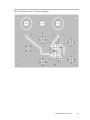
THS4503EVM User’s Guide June 2002 HPL SLOU132 IMPORTANT NOTICE Texas Instruments Incorporated and its subsidiaries (TI) reserve the right to make corrections, modifications, enhancements, improvements, and other changes to its products and services at any time and to discontinue any product or service without notice. Customers should obtain the latest relevant information before placing orders and should verify that such information is current and complete. All products are sold subject to TI’s terms and conditions of sale supplied at the time of order acknowledgment. TI warrants performance of its hardware products to the specifications applicable at the time of sale in accordance with TI’s standard warranty. Testing and other quality control techniques are used to the extent TI deems necessary to support this warranty. Except where mandated by government requirements, testing of all parameters of each product is not necessarily performed. TI assumes no liability for applications assistance or customer product design. Customers are responsible for their products and applications using TI components. To minimize the risks associated with customer products and applications, customers should provide adequate design and operating safeguards. TI does not warrant or represent that any license, either express or implied, is granted under any TI patent right, copyright, mask work right, or other TI intellectual property right relating to any combination, machine, or process in which TI products or services are used. Information published by TI regarding third−party products or services does not constitute a license from TI to use such products or services or a warranty or endorsement thereof. Use of such information may require a license from a third party under the patents or other intellectual property of the third party, or a license from TI under the patents or other intellectual property of TI. Reproduction of information in TI data books or data sheets is permissible only if reproduction is without alteration and is accompanied by all associated warranties, conditions, limitations, and notices. Reproduction of this information with alteration is an unfair and deceptive business practice. TI is not responsible or liable for such altered documentation. Resale of TI products or services with statements different from or beyond the parameters stated by TI for that product or service voids all express and any implied warranties for the associated TI product or service and is an unfair and deceptive business practice. TI is not responsible or liable for any such statements. Mailing Address: Texas Instruments Post Office Box 655303 Dallas, Texas 75265 Copyright 2002, Texas Instruments Incorporated EVM IMPORTANT NOTICE Texas Instruments (TI) provides the enclosed product(s) under the following conditions: This evaluation kit being sold by TI is intended for use for ENGINEERING DEVELOPMENT OR EVALUATION PURPOSES ONLY and is not considered by TI to be fit for commercial use. As such, the goods being provided may not be complete in terms of required design-, marketing-, and/or manufacturing-related protective considerations, including product safety measures typically found in the end product incorporating the goods. As a prototype, this product does not fall within the scope of the European Union directive on electromagnetic compatibility and therefore may not meet the technical requirements of the directive. Should this evaluation kit not meet the specifications indicated in the EVM User’s Guide, the kit may be returned within 30 days from the date of delivery for a full refund. THE FOREGOING WARRANTY IS THE EXCLUSIVE WARRANTY MADE BY SELLER TO BUYER AND IS IN LIEU OF ALL OTHER WARRANTIES, EXPRESSED, IMPLIED, OR STATUTORY, INCLUDING ANY WARRANTY OF MERCHANTABILITY OR FITNESS FOR ANY PARTICULAR PURPOSE. The user assumes all responsibility and liability for proper and safe handling of the goods. Further, the user indemnifies TI from all claims arising from the handling or use of the goods. Please be aware that the products received may not be regulatory compliant or agency certified (FCC, UL, CE, etc.). Due to the open construction of the product, it is the user’s responsibility to take any and all appropriate precautions with regard to electrostatic discharge. EXCEPT TO THE EXTENT OF THE INDEMNITY SET FORTH ABOVE, NEITHER PARTY SHALL BE LIABLE TO THE OTHER FOR ANY INDIRECT, SPECIAL, INCIDENTAL, OR CONSEQUENTIAL DAMAGES. TI currently deals with a variety of customers for products, and therefore our arrangement with the user is not exclusive. TI assumes no liability for applications assistance, customer product design, software performance, or infringement of patents or services described herein. Please read the EVM User’s Guide and, specifically, the EVM Warnings and Restrictions notice in the EVM User’s Guide prior to handling the product. This notice contains important safety information about temperatures and voltages. For further safety concerns, please contact the TI application engineer. Persons handling the product must have electronics training and observe good laboratory practice standards. No license is granted under any patent right or other intellectual property right of TI covering or relating to any machine, process, or combination in which such TI products or services might be or are used. Mailing Address: Texas Instruments Post Office Box 655303 Dallas, Texas 75265 Copyright 2002, Texas Instruments Incorporated EVM WARNINGS AND RESTRICTIONS It is important to operate this EVM within the input voltage range of 5 V and the output voltage range of +5 V and –5 V. Exceeding the specified input range may cause unexpected operation and/or irreversible damage to the EVM. If there are questions concerning the input range, please contact a TI field representative prior to connecting the input power. Applying loads outside of the specified output range may result in unintended operation and/or possible permanent damage to the EVM. Please consult the EVM User’s Guide prior to connecting any load to the EVM output. If there is uncertainty as to the load specification, please contact a TI field representative. During normal operation, some circuit components may have case temperatures greater than 50°C. The EVM is designed to operate properly with certain components above 50°C as long as the input and output ranges are maintained. These components include but are not limited to linear regulators, switching transistors, pass transistors, and current sense resistors. These types of devices can be identified using the EVM schematic located in the EVM User’s Guide. When placing measurement probes near these devices during operation, please be aware that these devices may be very warm to the touch. Mailing Address: Texas Instruments Post Office Box 655303 Dallas, Texas 75265 Copyright 2002, Texas Instruments Incorporated Information About Cautions and Warnings Preface About This Manual This manual provides information about using the THS4503 fully differential amplifier on evaluation module PCB marked with Edge # 6439396. Additionally, this document provides a good example of PCB design for high-speed applications. The user should keep in mind the following points. - The design of the high-speed amplifier PCB is a sensitive process. - The user must approach the PCB design with care and awareness. - It is recommended that the user initially review the data sheet of the device under test. - It is helpful to review the schematic and layout of the THS4503EVM to determine the design techniques used in the evaluation board. - It is recommended that the user review the application note Fully Differential Amplifiers (literature number SLOA054) to learn more about differential amplifiers. This application note reviews fully differential amps and presents calculations for various filters. How to Use This Manual This document contains the following chapters: - Chapter 1—Introduction and Description - Chapter 2—Using the THS4503EVM - Chapter 3—THS4503EVM Applications - Chapter 4—High-Speed Amplifier PCB Layout Tips - Chapter 5—EVM Hardware Description Information About Cautions and Warnings This book may contain cautions and warnings. This is an example of a caution statement. A caution statement describes a situation that could potentially damage your software or equipment. iii Related Documentation From Texas Instruments This is an example of a warning statement. A warning statement describes a situation that could potentially cause harm to you. The information in a caution or a warning is provided for your protection. Please read each caution and warning carefully. FCC Warning This equipment is intended for use in a laboratory test environment only. It generates, uses, and can radiate radio frequency energy and has not been tested for compliance with the limits of computing devices pursuant to subpart J of part 15 of FCC rules, which are designed to provide reasonable protection against radio frequency interference. Operation of this equipment in other environments may cause interference with radio communications, in which case the user at his own expense will be required to take whatever measures may be required to correct this interference. Electrostatic Sensitive Components This EVM contains components that can potentially be damaged by electrostatic discharge. Always transport and store the EVM in its supplied ESD bag when not in use. Handle using an antistatic wristband. Operate on an antistatic work surface. For more information on proper handling, refer to SSYA008. Related Documentation From Texas Instruments The URLs below are correct as of the date of publication of this manual. Texas Instruments applications apologizes if they change over time. - THS4503 data sheet (literature number SLOS350) - Application report (literature number SLOA054), Fully Differential Amplifiers - Application report (literature number SLOA069), How (Not) to Decouple High Speed Op Amp Circuits, http://www−s.ti.com/sc/psheets/sloa069/sloa069.pdf - Application report (literature number SLOA072), Single Supply Differen- tial Op Amp Techniques, http://www−s.ti.com/sc/psheets/sloa072/sloa072.pdf iv Trademarks - Application report (literature number SLMA002), Power Pad Thermally Enhanced Package, http://www−s.ti.com/sc/psheets/slma004/slma002.pdf - Application report (literature number SLMA004), Power Pad Made Easy, http://www−s.ti.com/sc/psheets/slma004/slma004.pdf - Application report (literature number SSYA008), Electrostatic Discharge (ESD), http://www−s.ti.com/sc/psheets/ssya008/ssya008.pdf Trademarks PowerPAD is a trademark of Texas Instruments. v vi Contents 1 Introduction and Description . . . . . . . . . . . . . . . . . . . . . . . . . . . . . . . . . . . . . . . . . . . . . . . . . . . . . 1.1 Description . . . . . . . . . . . . . . . . . . . . . . . . . . . . . . . . . . . . . . . . . . . . . . . . . . . . . . . . . . . . . . . . 1.2 Evaluation Module Features . . . . . . . . . . . . . . . . . . . . . . . . . . . . . . . . . . . . . . . . . . . . . . . . . 1.3 THS4503EVM Operating Conditions . . . . . . . . . . . . . . . . . . . . . . . . . . . . . . . . . . . . . . . . . . 1.4 EVM Default Configuration . . . . . . . . . . . . . . . . . . . . . . . . . . . . . . . . . . . . . . . . . . . . . . . . . . . 1-1 1-2 1-2 1-2 1-3 2 Using the THS4503EVM . . . . . . . . . . . . . . . . . . . . . . . . . . . . . . . . . . . . . . . . . . . . . . . . . . . . . . . . . . 2.1 Required Equipment . . . . . . . . . . . . . . . . . . . . . . . . . . . . . . . . . . . . . . . . . . . . . . . . . . . . . . . . 2.2 Power Supply Connection . . . . . . . . . . . . . . . . . . . . . . . . . . . . . . . . . . . . . . . . . . . . . . . . . . . 2.3 Function Generator Setup . . . . . . . . . . . . . . . . . . . . . . . . . . . . . . . . . . . . . . . . . . . . . . . . . . . 2.4 Signal Connection VIN− . . . . . . . . . . . . . . . . . . . . . . . . . . . . . . . . . . . . . . . . . . . . . . . . . . . . . 2-1 2-2 2-2 2-3 2-3 3 THS4503EVM Applications . . . . . . . . . . . . . . . . . . . . . . . . . . . . . . . . . . . . . . . . . . . . . . . . . . . . . . . 3-1 3.1 Single-Ended In/Single-Ended Out, Utilizing Transformer . . . . . . . . . . . . . . . . . . . . . . . . 3-2 3.2 Single-Ended to Fully Differential Application . . . . . . . . . . . . . . . . . . . . . . . . . . . . . . . . . . . 3-2 4 High-Speed Amplifier PCB Layout Tips . . . . . . . . . . . . . . . . . . . . . . . . . . . . . . . . . . . . . . . . . . . 4-1 5 EVM Hardware Description . . . . . . . . . . . . . . . . . . . . . . . . . . . . . . . . . . . . . . . . . . . . . . . . . . . . . . . 5-1 vii Contents 1−1. 2−1. 2−2. 3−1. 3−2. 3−3. 5−1. 5−2. 5−3. Schematic of the Populated Circuit on the EVM (Default Configuration) . . . . . . . . . . . . . . Power Supply Connection for ±5 Vdc . . . . . . . . . . . . . . . . . . . . . . . . . . . . . . . . . . . . . . . . . . . . Signal Connections . . . . . . . . . . . . . . . . . . . . . . . . . . . . . . . . . . . . . . . . . . . . . . . . . . . . . . . . . . . . Single-Ended In/Single-Ended Out, Utilizing Transformer . . . . . . . . . . . . . . . . . . . . . . . . . . . Sinlge Supply Operation . . . . . . . . . . . . . . . . . . . . . . . . . . . . . . . . . . . . . . . . . . . . . . . . . . . . . . . Output of an AC-Coupled, Single-Supply Application . . . . . . . . . . . . . . . . . . . . . . . . . . . . . . . Top Layer 1 (Signals for THS4503EVM) . . . . . . . . . . . . . . . . . . . . . . . . . . . . . . . . . . . . . . . . . . Bottom Layer 2 (Ground and Signal) . . . . . . . . . . . . . . . . . . . . . . . . . . . . . . . . . . . . . . . . . . . . . Schematic Diagram . . . . . . . . . . . . . . . . . . . . . . . . . . . . . . . . . . . . . . . . . . . . . . . . . . . . . . . . . . . 1-3 2-2 2-3 3-2 3-3 3-4 5-2 5-3 5-4 5−1 viii THS4503EVM Bill of Materials . . . . . . . . . . . . . . . . . . . . . . . . . . . . . . . . . . . . . . . . . . . . . . . . . . 5-1 Chapter 1 The Texas Instruments THS4503 evaluation module (EVM) helps designers evaluate the performance of the THS4503 fully differential operational amplifier (FDA). Also, this EVM is a good example of high-speed PCB design. This document details the THS4503EVM. It includes a list of EVM features, a brief description of the module illustrated with a series of schematic diagrams, EVM specifications, details on connecting and using the EVM, and a discussion of high-speed amplifier design considerations. This EVM enables the user to implement various circuits to clarify the available configurations presented by the schematic of the EVM. The user is not limited to the circuit configurations presented here. The EVM provides enough hardware hooks that the only limitation should be the creativity of the user. Topic Page 1.1 Description . . . . . . . . . . . . . . . . . . . . . . . . . . . . . . . . . . . . . . . . . . . . . . . . . . . 1-2 1.2 Evaluation Module Features . . . . . . . . . . . . . . . . . . . . . . . . . . . . . . . . . . . 1-2 1.3 THS4503EVM Operating Conditions . . . . . . . . . . . . . . . . . . . . . . . . . . . . 1-2 1.4 EVM Default Configuration . . . . . . . . . . . . . . . . . . . . . . . . . . . . . . . . . . . . . 1-3 Introduction and Description 1-1 Description 1.1 Description The THS4503EVM provides a platform for developing high-speed FDA application circuits. It contains the THS4503 high-speed FDA, a number of passive components, and various features and footprints that enable the user to experiment, test, and verify various operational amplifier circuit implementations. The PC board measures 3.08 by 2.42 inches. 1.2 Evaluation Module Features THS4503 high-speed operational amplifier EVM features include: - Wide operating supply voltage range: single supply 5 Vdc to dual supply ±5 Vdc operation (see the device data sheet). Single supply operation is obtained by placing a jumper from GND (J7) to –VS (J5). - Single-ended and fully differential input capability - Single-ended and fully differential output capability - Nominal 50-Ω input termination (R1||R2). Termination can be configured according to the application requirement. - VOCM direct input through TP1 - Output transformer T1 - Footprints for antialiasing filter implementation using locations R6, R7, C5, and C6 - Footprints for low pass filter implementation using locations C3, C4 - 800-Ω load provided through R8, R10, R9, and R11 reflected through T1 - Three convenient GND test points on the PCB - Power supply ripple rejection capacitors (C8 and C11) - Decoupling capacitors (C9, C12) populated with 0.1 µF capacitors— design final decoupling in accordance with SLOA069. - PowerPAD heatsinking capability - A good example of high-speed amplifier PCB design and layout 1.3 THS4503EVM Operating Conditions - Supply voltage range, ±VS 5 V to ±5 V (see the device data sheet) - Supply current, IS (see the device data sheet) For complete THS4503 amplifier IC specifications, parameter measurement information, and additional application information, see the THS4503 data sheet, TI literature number SLOS350. 1-2 EVM Default Configuration 1.4 EVM Default Configuration As delivered, the EVM has a fully functional example circuit, just add power supplies, a signal source, and monitoring instrument. See Figure 1−1 for the default schematic diagram. The user can change the gain by changing the ratios of the feedback and gain resistors (see the device data sheet for recommended resistor values). Chapter 5 has a complete EVM schematic diagram showing all component locations. The default configuration assumes a 50-Ω signal source and contains a termination resistor R1 for the source. Some components such as C8, C9, C11, C12, TP1, TP2, R10, T1, and J4 are omitted on the application schematics of Chapter 3 for clarity. Figure 1−1. Schematic of the Populated Circuit on the EVM (Default Configuration) TP3 TP2 PD− TP1 Vocm TP4 TP5 J7 GND R4 392Ω C13 1 µF C1 0 J1 Vin− R2 3 374Ω 1 − 2 Vocm 4 8 + 5 R1 56.2Ω C2 0 J6 Vin+ J2 Vout+ +VS R3 402Ω 6 R17 0 R6 0 U1 R8 4 T1 3 J4 Vout 340Ω R10 5 280Ω R7 0 R9 THS4503 6 340Ω 1 ADP4−1WT −VS J3 Vout− R5 392Ω J8 +VS +VS + C8 6.8µF C9 0.1µF J5 −VS −VS + C11 6.8µF C12 0.1µF Introduction and Description 1-3 1-4 Chapter 2 !" This section describes how to connect the THS4503EVM to test equipment. It is recommended that the user connect the EVM as described in this section to avoid damage to the EVM or the THS4503 installed on the board. Topic Page 2.1 Required Equipment . . . . . . . . . . . . . . . . . . . . . . . . . . . . . . . . . . . . . . . . . . 2-2 2.2 Power Supply Connection . . . . . . . . . . . . . . . . . . . . . . . . . . . . . . . . . . . . . 2-2 2.3 Function Generator Setup . . . . . . . . . . . . . . . . . . . . . . . . . . . . . . . . . . . . . 2-3 2.4 Signal Connection VIN− . . . . . . . . . . . . . . . . . . . . . . . . . . . . . . . . . . . . . . . . 2-3 Using the THS4503EVM 2-1 Required Equipment 2.1 Required Equipment - One dual-output dc power supply (±5 V, 1 A output minimum) - Two dc current meters with resolution to 1 mA and capable of the - maximum current the dc power supply can supply. 50-Ω source impedance function generator (1 MHz, 10 VPP sine wave) Oscilloscope (50-MHz bandwidth minimum, 50-Ω input impedance) 3 BNC-to-SMA cables BNC-to-BNC cable 5 Banana-to-Banana wires; 4 red, 1 black 2.2 Power Supply Connection (Refer to Figure 2−1) 1) Set the dual dc power supply to ±5 V. If available, set the current limit on the dc power supply to 100 mA. 2) Make sure the dual dc power supply is turned off before proceeding to the next step. 3) Connect the positive (+) terminal of the power supply to the positive (+) terminal of the current meter number 1. 4) Connect the negative (–) terminal of the current meter number 1 to +VS (J8). 5) Connect the common ground terminal of the power supply to GND (J7). 6) Connect the negative (–) terminal of the power supply to the negative (–) terminal of the second current meter. 7) Connect the positive (+) terminal of the current meter number 2 to –VS (J5). Figure 2−1. Power Supply Connection for ±5 Vdc 2-2 Function Generator Setup 2.3 Function Generator Setup Note: The oscilloscope inputs 1 and 2 must be set to 50-Ω input impedance for proper results. 1) Connect the function generator to oscilloscope channel 1. 2) Set vertical channels 1 and 2 of the oscilloscope to 0.2 V/division and the time-base to 0.1 µs/division. 3) Set the function generator to generate a 1-MHz, ±0.5 V (1 VPP) sine wave with no dc offset. 4) Verify that the output is 1 MHz, ±0.5 V (1 VPP). 5) Disable the function generator output before proceeding to the next step. 6) Disconnect the cable from the oscilloscope, retaining the setting of the function generator. 2.4 Signal Connection VIN− (Refer to Figure 2−2) 1) Using a BNC-to-SMA cable, connect the function generator to J1 (VIN−). 2) Using a BNC-to-SMA cable, connect the oscilloscope channel 1 to J2 (VOUT+). 3) Using a BNC-to-SMA cable, connect the oscilloscope channel 2 to J3 (VOUT−). Figure 2−2. Signal Connections Using the THS4503EVM 2-3 2-4 Chapter 3 !" # Example applications are presented in this chapter. These applications demonstrate the most popular circuits, but many other circuits can be constructed. The user is encouraged to experiment with different circuits, exploring new and creative design techniques. After all, that is the function of an evaluation board. Topic Page 3.1 Single-Ended In/Single-Ended Out, Utilizing Transformer . . . . . . . . . 3-2 3.2 Single-Ended to Fully Differential Application . . . . . . . . . . . . . . . . . . . 3-2 THS4503EVM Applications 3-1 Single-Ended In/Single-Ended Out, Utilizing Transformer 3.1 Single-Ended In/Single-Ended Out, Utilizing Transformer The fully differential amp output can be monitored by a single-ended instrument at J4. The THS4503EVM utilizes Mini-Circuits CD542 footprint transformers to make the fully differential to single-ended conversion. An ADP4−1WT transformer is installed on the board. R8, R9, and R10 are chosen such that the load on the fully differential amp is 800 Ω when combined with the load impedance transformed by the turn ratio T1. This load is chosen because it is a common input impedance value for ADCs, and is the impedance at which many fully differential amp parameters are measured. The 800-Ω load occurs when one of two conditions is met: - R11 is installed and the measuring instrument is set to 1-MΩ input impedance or - R11 is not installed and the measuring instrument has an input impedance of 50 Ω. Figure 3−1. Single-Ended In/Single-Ended Out, Utilizing Transformer TP1 Vocm R4 C13 1 µF J1 Vin− C1 0 3 374Ω 1 − 2 Vocm 4 8 + 5 R3 402Ω R17 0 392Ω R2 R1 56.2Ω C2 0 +VS 6 R6 0 U1 4 T1 3 J4 Vout 340Ω R10 5 280Ω R7 0 THS4503 R8 R9 R11 49.9Ω 6 1 340Ω ADP4−1WT −VS R5 392Ω 3.2 Single-Ended to Fully Differential Application The schematic of Figure 3−2 shows the proper technique for ac-coupling. The voltage present on the VOCM pin determines the dc operating point of the circuit. When no voltage is connected to TP1, the VOCM voltage level is determined by a voltage divider internal to the op amp, and is approximately equal to half of +VS. This dc voltage is present on both outputs, and also present on both inputs—being connected through R2 and R3. 3-2 Single-Ended to Fully Differential Application Figure 3−2. Single Supply Operation TP1 Vocm R4 392 W C13 1 mF C1 J1 Vin− 3 R2 374 W R1 56.2 W C2 +VS 1 2 8 R3 402 W R6 0 U1 4 − J2 Vout+ Vocm 5 + 6 R7 0 THS4503 J3 Vout− R17 0 R5 392 W Note: For this and some of the following circuits, it is necessary to install capacitors into locations designated as resistors, and vice versa. Because the capacitors and resistors come in the same case size, this should be easily accomplished. The designer should note that the ground connection of the schematic at C2 through R17 is a second input—to avoid confusion about whether a coupling capacitor is actually needed. In fact, there is no difference between single-ended and fully differential inputs to the board, except that the single-ended circuits utilize ground as signal return, while fully differential inputs utilize the other input as signal return. Any fully differential input to the board can be converted to a single-ended input merely by connecting one of the inputs to ground. This circuit allows the input voltage to swing below the negative power supply rail of the op-amp, as shown in Figure 3−3. THS4503EVM Applications 3-3 Single-Ended to Fully Differential Application Figure 3−3. Output of an AC-Coupled, Single-Supply Application 3 Volts 2 1 0 −1 0 500 n t − Time − s 1Ω The designer should realize that the coupling capacitors, acting with the gain resistors, produce a high pass characteristic into the circuit. This application circuit has interaction between Rsource, Rtermination, and Rg. Texas Instruments has provided an engineer design utility to facilitate the design of these circuits. Engineer design utilities are available on the Amplifiers and Comparators section of the Analog and Mixed Signal portion of the TI web page. Designers should be aware that each individual feedback path is an inverting path. There is no noninverting gain circuit for fully differential amps. The designer should also be aware that the gain is affected by the open loop characteristic of the FDA, the same as single−ended op amps. If there is sufficient safety margin between the closed loop response and open loop response of the FDA (40 dB or more), the error contribution from the open loop response of the FDA is negligible and can be ignored. 3-4 Chapter 4 $ #%& '( )* The THS4503EVM layout has been designed for use with high-speed signals and can be used as an example when designing PCBs incorporating the THS4503. Careful attention has been given to component selection, grounding, power supply bypassing, and signal path layout. Disregarding these basic design considerations could result in less than optimum performance of the THS4503 high-speed operational amplifier. Surfacemount components were selected because of the extremely low lead inductance associated with this technology. This helps minimize both stray inductance and capacitance. Also, because surface-mount components are physically small, the layout can be very compact. Tantalum power supply bypass capacitors at the power input pads help filter switching transients from the laboratory power supply. Power supply bypass capacitors are placed as close as possible to the IC power input pins in order to minimize the return path impedance. This improves high frequency bypassing and reduces harmonic distortion. The GND side of these capacitors should be located close to each other, minimizing the differential current loops associated with differential output currents. If poor high frequency performance is observed, replace the 0.1-µF capacitors with microwave capacitors with a self-resonance at the frequency that produces trouble. A proper ground plane on both sides of the PCB should be used with high-speed circuit design. This provides low-inductive ground connections for return current paths. In the area of the amplifier input pins, however, the ground plane has been removed to minimize stray capacitance and reduce ground plane noise coupling into these pins. This is especially important for the inverting input pin. As low as 1 pF capacitance at the inverting input can significantly affect the response of the amplifier or even oscillation. In general, it is best to keep signal lines as short and as straight as possible. Incorporation of microstrip or stripline techniques is also recommended when signal lines are greater than 1 inch in length. These traces must be designed with a characteristic impedance of either 50 Ω or 75 Ω, as required by the application. Such a signal line must also be properly terminated with an appropriate resistor. High-Speed Amplifier PCB Layout Tips 4-1 Circuit pathways should be made as symmetrical as possible for both feedback pathways to minimize second and other even-harmonic content. The printed-circuit board used with PowerPAD packages must have features included in the design to remove the heat from the package efficiently. As a minimum, there must be an area of solder-tinned-copper underneath the PowerPAD package. This area is called the thermal land. The thermal land varies in size depending on the PowerPAD package being used, the PCB construction and the amount of heat that needs to be removed. In addition, this thermal land may or may not contain thermal vias depending on PCB construction. The requirements for thermal lands and thermal vias are detailed in http://www−s.ti.com/sc/techlit/slma002 and http://www−s.ti.com/sc/techlit/slma004. Finally, all inputs and outputs must be properly terminated, either in the layout or in the load instrumentation. Unterminated lines, such as coaxial cable, can appear to be a reactive load to the amplifier. By terminating a transmission line with its characteristic impedance, the amplifier’s load then appears to be purely resistive, and reflections are absorbed at each end of the line. Another advantage of using an output termination resistor is that capacitive loads are isolated from the amplifier output. This isolation helps minimize the reduction in the amplifier’s phase-margin and improves the amplifier stability resulting in reduced peaking and settling times. 4-2 Chapter 5 !" + This chapter describes the EVM hardware. It includes the EVM parts list, and printed circuit board layout. Table 5−1. THS4503EVM Bill of Materials Item Description SMD Size Reference Designator PCB Qty. Manufacturer’s Part Number Distributor’s Part Number 1 CAP, 6.8 µF, tanatalum, 35 V, 10% D C8, C11 2 (AVX) TAJD685K035R (Garrett) TAJD685K035R 2 CAP, 0.1 µF, ceramic, X7R, 16 V 0508 C9, C12 2 (AVX) 0508YC104KAT2A (Garrett) 0508YC104KAT2A 3 Open 0805 C3, C4, C5, C6, C7, C10 6 4 Open 1206 C13, C14 2 5 Open 0805 R11, R12, R13, R14, R15, R16 6 6 Resistor, 0 Ω, 1/8 W 0805 C1, C2, R6, R7 4 (Phycomp) 9C08052A0R00JLHFT (Garrett) 9C08052A0R00JLHFT 7 Resistor, 280 Ω, 1/8 W, 1% 0805 R10 1 (Phycomp) 9C08052A2800FKHFT (Garrett) 9C08052A2800FKHFT 8 Resistor, 340 Ω, 1/8 W, 1% 0805 R8, R9 2 (Phycomp) 9C08052A3400FKHFT (Garrett) 9C08052A3400FKHFT 9 Resistor, 374 Ω, 1/8 W, 1% 0805 R2 1 (Phycomp) 9C08052A3740FKHFT (Garrett) 9C08052A3740FKHFT 10 Resistor, 392 Ω, 1/8 W, 1% 0805 R4, R5 2 (Phycomp) 9C08052A3920FKHFT (Garrett) 9C08052A3920FKHFT 11 Resistor, 402 Ω, 1/8 W, 1% 0805 R3 1 (Phycomp) 9C08052A4020FKHFT (Garrett) 9C08052A4020FKHFT 12 Resistor, 0 Ω, 1/4 W 1206 R17 1 (Phycomp) 9C12063A0R00JLHFT (Garrett) 9C12063A0R00JLHFT 13 Resistor, 56.2 Ω, 1/4 W, 1% 1206 R1 1 (Phycomp) 9C12063A56R2FKRFT (Garrett) 9C12063A56R2FKRFT 14 Transformer, 4:1 CD542 T1 1 (Mini-Circuits) ADT4−1WT (Mini-Circuits) ADT4−1WT 15 Test points (black) TP3, TP4, TP5 3 (Keystone) 5001 (Allied) 839−3601 16 Test points (red) TP1, TP2 2 (Keystone) 5000 (Allied) 839−3600 EVM Hardware Description 5-1 Item Description SMD Size Reference Designator PCB Qty. Manufacturer’s Part Number Distributor’s Part Number 17 Jack, banana receptacle, 0.25” diameter hole J5, J7, J8 3 (HH Smith) 101 (Newark) 35F865 18 Connector, SMA PCB Jack J1, J2, J3, J4, J6 5 (Amphenol) 901−144−8RFX (Newark) 01F2208 19 Standoff, 4−40 Hex, 0.625” Length 4 (Keystone) 1804 (Allied) 839−2089 20 Screw, Phillips, 4−40, .250” 4 SHR−0440−016−SN 21 IC, THS4503 1 (TI) THS4503DGN 22 Board, printed circuit 1 (TI) EDGE # 6439396 U1 Figure 5−1. Top Layer 1 (Signals for THS4503EVM) 5-2 Figure 5−2. Bottom Layer 2 (Ground and Signal) EVM Hardware Description 5-3 Figure 5−3. Schematic Diagram VCC+ R13 * C13 1 µF TP2 PD− TP1 Vocm J7 GND R15 * C4 * R14 * TP3 TP4 TP5 VCC+ R16 * R4 C14 * 392Ω J2 Vout+ +VS C1 0 J1 Vin− R2 3 374Ω 1 − 2 Vocm 8 + R1 56.2Ω C2 0 J6 Vin+ R3 402Ω 4 R8 C5 * 5 THS4503 6 R17 0 R6 0 U1 R7 0 C6 * 4 T1 3 J4 Vout 340Ω C7 * R9 340Ω R10 280Ω 5 R11 * 6 1 ADP4 −1WT J3 Vout− −VS R5 392Ω C3 * J8 +VS Note: 5-4 + C8 6.8µF +VS C9 0.1µF C10 * J5 −VS + C11 6.8µF C12 0.1µF −VS R12 * Devices designated with an * are not installed on the EVM. The user must supply these components.