1
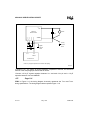
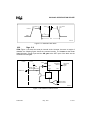
8XC196KC
SPECIFICATION UPDATE
Release Date: May, 1997
Order Number: 272834-004
The 8XC196KC may contain design defects or errors known as errata. Characterized
errata that may cause the 8XC196KC’s behavior to deviate from published specifications are documented in this specification update.
Information in this document is provided in connection with Intel products. No license, express or implied, by
estoppel or otherwise, to any intellectual property rights is granted by this document. Except as provided in Intel’s
Terms and Conditions of Sale for such products, Intel assumes no liability whatsoever, and Intel disclaims any
express or implied warranty, relating to sale and/or use of Intel products including liability or warranties relating to
fitness for a particular purpose, merchantability, or infringement of any patent, copyright or other intellectual
property right. Intel products are not intended for use in medical, life saving, or life sustaining applications.
Intel retains the right to make changes to specifications and product descriptions at any time, without notice.
Contact your local Intel sales office or your distributor to obtain the latest specifications before placing your
product order.
*Third-party brands and names are the property of their respective owners.
Copies of documents which have an ordering number and are referenced in this document, or other Intel
literature, may be obtained from:
Intel Corporation
P.O. Box 7641
Mt. Prospect IL 60056-7641
or call in North America 1-800-879-4683, Europe 44-0-1793-431-155,
France 44-0-1793-421-777, Germany 44-0-1793-421-333, other countries 708-296-9333
Copyright © 1996, INTEL CORPORATION
May, 1997
272834-004
8XC196KC SPECIFICATION UPDATE
CONTENTS
CONTENTS ..............................................................................................iii
REVISION HISTORY .................................................................................1
PREFACE ..................................................................................................2
SUMMARY TABLE OF CHANGES ...........................................................4
IDENTIFICATION INFORMATION ..........................................................10
ERRATA ..................................................................................................11
SPECIFICATION CHANGES ..................................................................31
SPECIFICATION CLARIFICATIONS ......................................................31
DOCUMENTATION CHANGES ..............................................................39
272834-004
May, 1997
iii
8XC196KC SPECIFICATION UPDATE
REVISION HISTORY
This Specification Update supersedes TechBit MC3191 (Notes CWFME1) and contains all
the known errata for the 8XC196KC and 8E196KC devices.
Rev. Date Version
07/01/96
001
11/13/96
002
03/12/97
003
05/13/97
004
272834-004
Description
This is the new Specification Update document. It contains all
identified errata published prior to this date.
Corrected the table, Errata - Part I, and reformatted the table to fit
on a single page for readability. Note that Errata - Part I shows the
products and steppings to which each erratum applies, while
Errata - Part II provides a brief description of each erratum and
the page number for its associated description.
Corrections were made to the errata and identification information
markings summary tables.
Documentation change 054 and specification clarification 022.
May, 1997
1 of 51
8XC196KC SPECIFICATION UPDATE
PREFACE
As of July, 1996, Intel’s Semiconductor Products Group has consolidated available
historical device and documentation errata into this new document type called the Specification Update. We have endeavored to include all documented errata in the consolidation
process, however, we make no representations or warranties concerning the
completeness of the Specification Update.
This document is an update to the specifications contained in the Affected
Documents/Related Documents table below. This document is a compilation of device
and documentation errata, specification clarifications and changes. It is intended for
hardware system manufacturers and software developers of applications, operating
systems, or tools.
Information types defined in Nomenclature are consolidated into the specification update
and are no longer published in other documents.
This document may also contain information that was not previously published.
Affected Documents/Related Documents
Title
Order
8XC196KC/KC20 Commercial/Express CHMOS Microcontroller
datasheet
Embedded Microcontrollers
8XC196KC/KD User’s Manual (1992)
8XC196KC Quick Reference
80C196KC User’s Guide
8XC196KB/KC/KD Programming Support Fact Sheet
Development Tools Handbook
ApBUILDER Interactive Application Programming Package Disk
Project Builder 196 “FREE” Demo Software
270942
270646
272238
272112
270704
272225
272326
272216
272329
Nomenclature
Errata are design defects or errors. These may cause the published (component, board,
system) behavior to deviate from published specifications. Hardware and software
designed to be used with any component, board, and system must consider all errata
documented.
2 of 51
May, 1997
272834-004
8XC196KC SPECIFICATION UPDATE
Specification Changes are modifications to the current published specifications. These
changes will be incorporated in any new release of the specification.
Specification Clarifications describe a specification in greater detail or further highlight
a specification’s impact to a complex design situation. These clarifications will be incorporated in any new release of the specification.
Documentation Changes include typos, errors, or omissions from the current published
specifications. These will be incorporated in any new release of the specification.
NOTE:
Errata remain in the specification update throughout the product’s lifecycle, or until a
particular stepping is no longer commercially available. Under these circumstances, errata
removed from the specification update are archived and available upon request. Specification changes, specification clarifications and documentation changes are removed from
the specification update when the appropriate changes are made to the appropriate
product specification or user documentation (datasheets, manuals, etc.).
272834-004
May, 1997
3 of 51
8XC196KC SPECIFICATION UPDATE
SUMMARY TABLE OF CHANGES
The following table indicates the errata, specification changes, specification clarifications,
or documentation changes which apply to the 8XC196KC product. Intel may fix some of
the errata in a future stepping of the component, and account for the other outstanding
issues through documentation or specification changes as noted. This table uses the
following notations:
Codes Used in Summary Table
Stepping
X:
(No mark) or (Blank box):
Errata exists in the stepping indicated. Specification Change
or Clarification that applies to this stepping.
This erratum is fixed in listed stepping or specification change
does not apply to listed stepping.
Page
(Page):
Page location of item in this document.
Status
Doc:
Fix:
Fixed:
NoFix:
Eval:
Document change or update will be implemented.
This erratum is intended to be fixed in a future step of the component.
This erratum has been previously fixed.
There are no plans to fix this erratum.
Plans to fix this erratum are under evaluation.
Row
Change bar to left of table row indicates this erratum is either
new or modified from the previous version of the document.
4 of 51
May, 1997
272834-004
8XC196KC SPECIFICATION UPDATE
Errata - Part I
D0
A1
D0
D0
D1
B
E
A
B
C
D
B
G
H
J
K
L
M
N
U
80C196KC
80C196KC
83C196KC
87C196KC
83C196KC
87C196KC
X
X
X
X
X
X
X
X
X
C3
80C196KC
X
X
X
X
X
R
X
X
X
X
X
X
X
X
X
X
X
B2
80C196KC
X
X
X
X
B3
87C196KC
X
X
X
R
B2
87C196KC
101
109
115
116
123
126
131
132
140
143
147
150
163
173
174
175
176
177
178
179
180
181
182
214
215
216
300
300
300
300
300
300
300
B1
87C196KC
9600001
9600002
9600003
9600004
9600005
9600006
9600007
9600008
9600009
9600010
9600011
9600012
9600013
9600014
9600015
9600016
9600017
9600018
9600019
9600020
9600021
9600022
9600023
9600024
9600025
9600026
9600027
9600028
9600029
9600030
9600031
9600032
9600033
B
8EC196KC
Old
#
A
8EC196KC
ID
87C196KC
Number
A
8EC196KC
Products and Steppings
A
X
X
X
R
X
X
X
X
X
X
X
R
X
X
X
X
X
X
X
X
X
X
X
X
X
X
X
X
X
X
X
X
X
X
X
X
X
R
X
X
X
X
X
X
X
X
X
X
X
R
X
X
X
X
X
X
X
X
X
X
X
X
X
X
X
X
X
X
X
X
X
X
X
X
X
X
X
X
X
X
X
X
X
X
X
X
X
X
X
X
X
X
X
X
X
X
X
R
X
X
X
R
X
X
X
X
X
X
X
X
X
X
X
X
X
X
X
X
X
X
X
X
X
X
X
X
X
R
R
R
R
R
Status
Fixed
Fixed
Fixed
NoFix
Fixed
Fixed
Fixed
Fixed
Fixed
Fixed
NoFix
Fixed
Fixed
Fixed
Fixed
Fixed
Fixed
Fixed
Fixed
Fixed
Fixed
Fixed
Fixed
Fixed
Fixed
Fixed
Fixed
Fixed
NoFix
NoFix
NoFix
NoFix
Fixed
“R” identifies the stepping in which a problem was first reported.
272834-004
May, 1997
5 of 51
8XC196KC SPECIFICATION UPDATE
Errata - Part II
Number
Old #
Page
9600001
9600002
9600003
9600004
9600005
9600006
9600007
9600008
9600009
9600010
9600011
9600012
9600013
9600014
9600015
9600016
9600017
9600018
9600019
9600020
9600021
9600022
9600023
9600024
9600025
9600026
9600027
9600028
9600029
9600030
9600031
9600032
9600033
101
109
115
116
123
126
131
132
140
143
147
150
163
173
174
175
176
177
178
179
180
181
182
214
215
216
300
300
300
300
300
300
300
11
11
12
12
12
13
13
14
15
15
15
17
17
18
18
18
19
19
19
20
20
20
21
21
21
25
25
26
27
27
29
29
30
6 of 51
Errata
A/D Cancel Error
Divide Error With HOLD# or READY
HSO IOC1 Bits Interchanged
Indirect Shift Count Value
NMI During PTS Skips an Address
Port 0 Latched on Wrong Phase
PTS Request During Interrupt Latency
NMI During PTS Latency
SIO RI Flag
TIJMP INDEX_MASK Value Limitation
Write Cycle During Reset
Serial Port Framing Error
Glitch on Quasi-bidirectional (QBD) Port Pins During Power Up
A/D Linearity
Analog Input Latch-up
INST Weakly Driven Low During CCB Fetch
2 CCB Fetches
3 Wait States During CCB Fetch
ALE, RD#, WR#, BHE, INST, TXD Pullup Too Weak During Reset
Buswidth Is Permanently 16 Bits
Glitch on VCC Will Cause Device Reset
Incomplete Reset At > 12MHz
Default Buswidth Out of Reset is 16 Bits
ONCE Mode Entry
Oscillator Noise Sensitivity
Reset Hysteresis
Port 0 CMOS Level
Missing External Interrupt Requests (EXTINT, EXTINT1, NMI)
BMOVI Windowing Count Register
HSI Events (9 or more)
SIO Mode 0 Maximum Baud Rate
Writing HSI_MODE Resets Divide-by-Eight Counter
IPD Hump
May, 1997
272834-004
8XC196KC SPECIFICATION UPDATE
Specification Changes
Steppings
Number
Page
#
#
Status
Specification Changes
#
None for this revision of this specification update.
Specification Clarifications
Steppings
Number
Page
#
001
002
003
004
005
006
007
008
009
010
011
012
013
014
015
016
017
018
019
020
021
022
272834-004
#
Status
Specification Clarifications
#
31
31
32
33
33
33
34
34
35
36
36
36
36
36
37
38
38
38
38
38
38
38
Doc
Doc
Doc
Doc
Doc
Doc
Doc
Doc
Doc
Doc
Doc
Doc
Doc
Doc
Doc
Doc
Doc
Doc
Doc
Doc
Doc
Spec. Clarifications 001-021 apply to document number
272238-001, 8XC196KC/KD User’s Manual.
Page 5-10
Page 8-4
Page 8-18
Page 9-3
Page 10-2
Page 11-3
Page 12-1
Page 13-4
Page 13-22
Page 14-15
Page 14-17
Page 14-31
Page 14-33
Page B-9
Page B-9
Page C-5
Page C-16
Page C-33
Page C-37
Page C-45
Page C-51
Specification changes in Table 14-12.
May, 1997
7 of 51
8XC196KC SPECIFICATION UPDATE
Documentation Changes
(1 of 2)
Number
Document Revision
Page
Status
001
002
003
004
005
006
007
008
009
010
011
012
013
014
015
016
017
018
019
020
021
022
023
024
025
026
027
028
029
030
031
032
033
034
035
036
037
272338-001
272338-001
272338-001
272338-001
272338-001
272338-001
272338-001
272338-001
272338-001
272338-001
272338-001
272338-001
272338-001
272338-001
272338-001
272338-001
272338-001
272338-001
272338-001
272338-001
272338-001
272338-001
272338-001
272338-001
272338-001
272338-001
272338-001
272338-001
272338-001
272338-001
272338-001
272338-001
272338-001
272338-001
272338-001
272338-001
272338-001
40
40
40
40
40
41
41
41
41
42
42
42
42
42
43
43
43
43
43
44
44
44
44
45
45
45
46
47
48
48
48
48
48
48
48
48
49
Doc
Doc
Doc
Doc
Doc
Doc
Doc
Doc
Doc
Doc
Doc
Doc
Doc
Doc
Doc
Doc
Doc
Doc
Doc
Doc
Doc
Doc
Doc
Doc
Doc
Doc
Doc
Doc
Doc
Doc
Doc
Doc
Doc
Doc
Doc
Doc
Doc
8 of 51
Documentation Changes
Page 4-1
Page 4-2
Page 4-4
Page 4-9
Page 5-4
Page 5-6
Page 5-7
Page 5-7
Page 5-8
Page 5-9
Page 5-16
Page 5-16
Page 5-18
Page 5-19
Page 5-25
Page 5-26
Page 6-10
Page 7-1
Page 7-8
Page 7-9
Page 8-11
Page 9-2
Page 10-2
Page 11-1
Page 11-2
Page 11-3
Page 11-6
Page 11-8
Page 12-2
Page 12-7
Page 13-2
Page 13-9
Page 14-9
Page 14-11
Page 14-12
Page 14-15
Page 14-19
May, 1997
272834-004
8XC196KC SPECIFICATION UPDATE
Documentation Changes
(2 of 2)
Number
Document Revision
Page
Status
038
039
040
041
042
043
044
045
046
047
048
049
050
051
052
053
054
272338-001
272338-001
272338-001
272338-001
272338-001
272338-001
272338-001
272338-001
272338-001
272338-001
272338-001
272338-001
272338-001
272338-001
272338-001
272338-001
272834-004
49
49
49
49
49
49
49
50
50
50
50
50
50
51
51
51
51
Doc
Doc
Doc
Doc
Doc
Doc
Doc
Doc
Doc
Doc
Doc
Doc
Doc
Doc
Doc
Doc
272834-004
Documentation Changes
Page 14-29
Page A-23
Page A-28
Page A-35
Page A-36
Page A-37
Page A-38
Page A-39
Page A-45
Page B-6
Page C-14
Page C-45
Page C-55
Page C-56
Page C-57
Page C-65
Subtitle change on page 8-23.
May, 1997
9 of 51
8XC196KC SPECIFICATION UPDATE
IDENTIFICATION INFORMATION
Markings
10 of 51
Product
Stepping
Marking (FPO Number Suffix)
8EC196KC - P629.5, F6
8EC196KC - P629.5, F6
8EC196KC - P629.5, F6
87C196KC - P629.5, F6
87C196KC - P629.5, F6
87C196KC - P629.5, F6
87C196KC - P629.5, F6
80C196KC - P629.9, F6
80C196KC - P629.9, F6
80C196KC - P648.6, F9
80C196KC - Alternate
83C196KC - P629.9, F6
87C196KC - P629.5, F6
83C196KC - P648.6, F9
83C196KC - Alternate
83C196KC - P648.6, F9
83C196KC - P648.18, F8
80C196KC - P648.6, F8
83C196KC - P629.9s, F6
87C196KC - P629.8s, F6
80C196KC - P648.39, F8
83C196KC - P648.39, F8
A
B
B-2
A
B-1
B-2
B-3
C-3
D-0
A-1
D-0
D-0
D-1
B
D-1
B
C
A-1
E-0
E-0
E
F
none
A
B
A or none
B
C
D
G
H
J
K
L
M
N
Q
R (Has all fixes of 83C196KC B)
T (Has all fixes of 83C196KC B)
U (Has all fixes of 83C196KC B)
U (Has all fixes of 83C196KC D-0)
U
W (Has all fixes of 83C196KC B)
none
May, 1997
272834-004
8XC196KC SPECIFICATION UPDATE
ERRATA
9600001.
A/D Cancel Error
PROBLEM: If a new A/D conversion is started before the previous conversion is
complete, the results may be incorrect.
IMPLICATION: All customers using the A/D are affected. Additional software overhead
required. Could delay conversion start time.
WORKAROUND: Never start a new conversion until the previous one is finished. This
can be accomplished by polling the A/D Done bit or with an interrupt.
STATUS: This has been fixed. Refer to Summary Table of Changes to determine the
affected stepping(s).
9600002.
Divide Error With Hold# or Ready
PROBLEM: Result of a signed divide may be off by one if executed while device is held
off the bus by HOLD# or READY and the queue is empty. Specific timings of HOLD# or
READY going active and inactive must also be met. There are no generic symptoms. The
effect will vary depending on how the divide results are used.
IMPLICATION: Customer using HOLD# or READY and a signed divide instruction will be
affected. The customer impact varies according to each application.
WORKAROUND: The problem occurs only in a one-state-time window when DIV or DIVB
is the last instruction in the prefetch queue while HOLD# or READY is active.
If HOLD# and READY are not used, the result is always correct. In the case of READY,
the problem does not occur if READY is programmed to insert 0, 1, 2, or 3 wait states.
The error may occur when infinite number of wait states are selected and 14 or more
waitstates are asserted.
For the applications that use HOLD# and the divide instruction, a simple workaround is to
disable hold before every divide and enable it after the divide is complete. Assuming an
application enables HOLD# throughout the entire program, the following piece of code
disables hold before a divide instruction and enables hold when the divide instruction
finishes executing.
HLDEN_BIT
EQU
WSR
EQU
14H
...
ANDB
WSR,#NOT HLDEN_BIT
NOP
272834-004
80H
May, 1997
11 of 51
8XC196KC SPECIFICATION UPDATE
DIV
ORB
...
XX,
YY,
ZZ
WSR,#HLDEN_BIT
;DIVB if byte operation is desired.
The NOP instruction is necessary to give the HLDEN bit time to change.
For applications that use READY, the simplest solution is to avoid infinite wait states.
STATUS: This has been fixed. Refer to Summary Table of Changes to determine the
affected stepping(s).
9600003.
HSO IOC1 Bits Interchanged
PROBLEM: HSO IOC1 register bits 4 and 6 are interchanged. HSO.4/HSI.2 or
HSO.5/HSI.3 not enabled when expected.
IMPLICATION: Any customer using HSO.4/HSI.2 and HSO.5/HSI.3 will be affected.
Software change for customers using HSO.4/HSI.2 or HSO.5/HSI.3.
WORKAROUND: Need to redefine these bits in the assembler source code.
STATUS: This has been fixed. Refer to Summary Table of Changes to determine the
affected stepping(s).
9600004.
Indirect Shift Count Value
PROBLEM: The SHRL and SHLL instructions function correctly with count values 0-31,
inclusive. However, a shift count value of XX100000b causes 32 shifts, which results in no
shift taking place. With all other count values, the upper 3 bits are masked off and the
remaining bits specify the number of shifts. Also, a shift count value of XX1XXXXXB
causes the overflow flag and the overflow-trap flag to be set.
IMPLICATION: Customers using SHRL and SHLL instructions with a count value greater
than 31 will be affected.
WORKAROUND: Ensure that the count value never exceeds 31.
STATUS: There are no plans to fix this. Refer to Summary Table of Changes to determine
the affected stepping(s).
9600005.
NMI During PTS Skips an Address
PROBLEM: When NMI interrupts a PTS routine, the first byte of the instruction following
completion of the PTS cycle is lost. Incorrect code execution following NMI.
12 of 51
May, 1997
272834-004
8XC196KC SPECIFICATION UPDATE
IMPLICATION: Any customer using the PTS and NMI will be affected. NMI cannot be
used during a PTS cycle.
WORKAROUND: NMI must be disabled using external hardware during any PTS activity.
Practically, this means that NMI cannot be used in any designs that uses the PTS.
STATUS: This has been fixed. Refer to Summary Table of Changes to determine the
affected stepping(s).
9600006.
Port 0 Latched on Wrong Phase
PROBLEM: Port 0 is not latched on the correct phase. This causes problems when it is
used as a digital input port. Digital data is not read in correctly on port 0.
IMPLICATION: Any customer using port 0 for digital input will be affected. Designs may
need external synchronization circuitry.
WORKAROUND: If data remains stable on the port while CLKOUT is high, the data will
be read correctly.
STATUS: This has been fixed. Refer to Summary Table of Changes to determine the
affected stepping(s).
9600007.
PTS Request During Interrupt Latency
PROBLEM: If a request for a PTS cycle occurs during a normal interrupt service latency,
the device vectors incorrectly. The device executes the interrupt service routine (ISR)
instead of servicing the interrupt by the PTS. The interrupt pending bit may be cleared by
the vector to the ISR, but the PTSSEL bit will still be valid. These will vary according to the
application but in general the number of PTS cycles that should have occurred didn’t. In
some applications this manifests itself as:
Too few A/D results stored for A/D scan mode.
Too few bytes/words transferred to or from the peripherals or memory.
Some can be very difficult to identify. Situations will exist where old data from previously
completed PTS cycles may mask when short PTS cycles occur.
IMPLICATION: Any customer that uses the PTS while other interrupts are enabled will be
affected. With the workaround in place, the only effect to the customer will be an
occasional increase in the PTS response time. Without the workaround in place, the effect
will be dependent on the application.
272834-004
May, 1997
13 of 51
8XC196KC SPECIFICATION UPDATE
WORKAROUND: For every interrupt source that is serviced by the PTS, the ISR must be
modified to examine the PTSSEL bits. If the PTSSEL bit is set, the error has occurred.
The code must then set the interrupt pending bit and exit the ISR. Upon exit, the PTS will
then handle the interrupts as originally intended. If the PTSSEL bit is not set, then the
count must have reached zero and the interrupt should be handled normally.
The following software solves this problem:
PTSx_ISR:PUSHA
LDB WSR,#01H
JBS PTSSEL,PTSx_BIT,PTXx_ABORT
;GET HWINDOW1
;SEE IF PTSSEL BIT IS SET
;NO, OK TO CONTINUE
PTSx_COUNT0:
;PTS COUNT = 0
LDB WSR,R0
;CLEAR WSR (IF NEEDED)
;*****************************
;PLACE NORMAL ISR ROUTINE HERE
;FOR SERVICING PTSCB, ETC
;******************************
;
POPA
RET
PTSx_ABORT:
;***********************************************
;THIS ROUTINE ENTERED IF PTSSEL BIT WAS SET.
;CODE NEEDS TO FORCE ANOTHER PTS CYCLE BY
;SETTING THE INTERRUPT PENDING BIT CORRESPONDING
;TO THE INTERRUPT THAT GOT US HERE!
;************************************************
;
ORB INT_PEND,#PTSx_BIT_MASK
;"INT_PEND" COULD BE
;INT_PEND1 OR EPA_PEND
POPA
RET
STATUS: This has been fixed. Refer to Summary Table of Changes to determine the
affected stepping(s).
9600008.
NMI During PTS Latency
PROBLEM: If an NMI occurs during the PTS latency, it is possible that the pending NMI
bit is cleared while never being serviced or the NMI is serviced and the PTS pending bit is
cleared and never serviced. NMI will not be serviced 100% of the time or PTS cycles will
be missed.
IMPLICATION: Customers who have not tied NMI low and who are using the PTS will be
affected. NMI cannot be used while the PTS is active.
14 of 51
May, 1997
272834-004
8XC196KC SPECIFICATION UPDATE
WORKAROUND: Force NMI low whenever the PTS is enabled.
STATUS: This has been fixed. Refer to Summary Table of Changes to determine the
affected stepping(s).
9600009.
SIO RI Flag
PROBLEM: This problem occurs only in mode 0 if the value is greater than 8006H (slower
baud rate). After receiving the first byte of data, the RI will not be generated again. The
effect is that only one byte of data will be received and then the logic will hang up.
IMPLICATION: All customers using the SIO in synchronous mode (mode 0) and with a
BAUD_RATE value greater than 8006H will be affected. Additional code is required in the
SIO interrupt service routine.
WORKAROUND: Reinitialize the baud rate register after reading the character in SBUF.
This is done by writing two bytes to BAUD_RATE (0EH, Hwindow 0). This action will reset
the mode 0 SIO logic.
STATUS: This has been fixed. Refer to Summary Table of Changes to determine the
affected stepping(s).
9600010.
TIJMP INDEX_MASK Value Limitation
PROBLEM: If the value of the INDEX_MASK in the TIJMP instruction is greater than 7FH,
the table address will be incorrectly calculated. Incorrect operation of the TIJMP
instruction.
IMPLICATION: Any customer who uses the TIJMP instruction will be affected. Code may
have to be modified to ensure that INDEX_MASK is 7FH or less.
WORKAROUND: Change INDEX_MASK value to be 7FH or less.
STATUS: This has been fixed. Refer to Summary Table of Changes to determine the
affected stepping(s).
9600011.
Write Cycle During Reset
PROBLEM: The data bus floats asynchronously with RESET#. If reset occurs during an
external write cycle, the contents of the external device may be corrupted. This is the
normal operating condition for reset, and is not considered a bug. It is included on this list
for those customers who may encounter corruption of data in external RAM during reset.
272834-004
May, 1997
15 of 51
8XC196KC SPECIFICATION UPDATE
IMPLICATION: Anyone who resets a system while writing to external RAM will be
affected. May have to add external circuitry if this is a problem.
WORKAROUND: Allow reset to occur only at the rising edge of CLKOUT and only if WR#
is high. If a reset occurs during an external bus write cycle, RAM data on the external bus
may be corrupted. This describes a logic design that will alleviate the problem.
The following circuit will allow a manual reset to occur at the rising edge of CLKOUT only
if WR# is high (inactive). If WR# is low (active) then RESET# will stay high (inactive). The
74HC14 and 74HC05 are usually already in the system, so the only additional
components are the 74AC74, R1, and C1.
VCC
VCC
R1=10K
R3
74HC05
R2
SW1
S
C1=100pF
VCC
D
RESET#
Q
74HC14
CL
C2
Q#
R
(RESET#)
74AC74
CLKOUT
WR#
A4352-01
Notes:
1. R1 = 10K ohms and C1 = 100 pF.
2. R2 and C2 should allow for reset state times plus write wait states.
If software resets can occur, use RESET#. If no software resets will occur, eliminate the
74HC05 and use (RESET#).
The R1*C1 time constant is one microsecond to ensure that the flip-flop comes up ’on’
after a power-up. The reset flip-flop at the rising edge of CLKOUT after the R2*C2 time
constant has expired.
16 of 51
May, 1997
272834-004
8XC196KC SPECIFICATION UPDATE
For manual resets, the flip-flop will turn on at the next rising edge of CLKOUT unless WR#
is low. If WR# is low, the flip-flop turn on will be delayed until the next rising edge of
CLKOUT when WR# is not low. This may occur after any number of wait states. The
R2*C2 time constant must be long enough for the normal reset state times plus the
maximum number of write wait states.
STATUS: There are no plans to fix this. Refer to Summary Table of Changes to determine
the affected stepping(s).
9600012.
Serial Port Framing Error
PROBLEM: The stop bit in a normal receive frame is a ‘1’. If a ‘0’ is received instead of an
expected stop bit, the serial port should recognize the ‘0’ as a framing error and set the
framing error flag.
An error occurs when the last data bit preceding a stop bit is a ‘1’ and the RXD line
glitches low, causing an erroneous ‘0’ stop bit. When this occurs, the receiver interprets
the erroneous ‘0’ stop bit as the first data bit for the next frame, corrupting the next frame.
IMPLICATION: Any customer using the serial port will be affected.
WORKAROUND:
1. Use 8-bit mode with parity disabled and use the 7-bit ASCII character set.
2. Use 9-bit mode and set the 9th data bit to '0'.
STATUS: This has been fixed. Refer to Summary Table of Changes to determine the
affected stepping(s).
9600013.
Glitch on Quasi-bidirectional (QBD) Port Pins During Power Up
PROBLEM: There is a strong negative glitch on all QBD port pins (P1.x, P2.6, P2.7) on
the first falling CLKOUT edge following powerup. This glitch lasts about 5 ns, and only
occurs one time following initial application of VCC. Although the glitch is short, the time for
the pin to return to VCC may be several microseconds, depending on the pin loading
capacitance. External devices connected to QBD pins may react to this glitch during
power up. Exact symptoms will vary, depending on the design.
IMPLICATION: All customers who are using QBD port pins will be affected. External
hardware design may have to be altered to allow for this glitch.
WORKAROUND: External systems and devices should be disabled from responding to
this glitch until after the first CLKOUT falling edge has occurred. One way to do this is to
hold the system in reset until the oscillator has stabilized. The length of the glitch can be
272834-004
May, 1997
17 of 51
8XC196KC SPECIFICATION UPDATE
controlled by a pullup to VCC, but stay within the VOL and IOL total (port) current limit specifications.
STATUS: Fixed. Refer to Summary Table of Changes to determine affected stepping(s).
9600014.
A/D Linearity
PROBLEM: A/D linearity and absolute error are unacceptably large (±8 LSB in 10-bit
mode). Incorrect A/D conversion results.
IMPLICATION: Anyone using the A/D converter will be affected. May require special
circuitry to maintain VREF within ± 0.25 volts of VCC. May require more stable VCC supply.
WORKAROUND: If VREF is held within ± 0.25 volts of VCC,, absolute error is improved to
± 3 LSB in 10-bit mode.
STATUS: Fixed. Refer to Summary Table of Changes to determine affected stepping(s).
9600015.
Analog Input Latch-up
PROBLEM: Inputs ACH6 and ACH7 to the A/D converter will latch up. The effects are
poor A/D performance, ACH6 and ACH7 inputs latched up, high input current.
IMPLICATION: Any customer using the A/D converter will be affected. System design
may have to be modified to prevent latch-up on these pins.
WORKAROUND: Voltage must not be applied to ACH6 or ACH7 before VCC is stable.
STATUS: Fixed. Refer to Summary Table of Changes to determine affected stepping(s).
9600016.
INST Weakly Driven Low During CCB Fetch
PROBLEM: The INST pin is weakly driven low during the CCB fetch. The weak pulldown
will sink about 100 µA and remain at VCL. CCB can be loaded from wrong memory bank
on systems using INST.
IMPLICATION: Any customer using INST will be affected. Applications using INST to
separate code and data space may not read in the correct CCB. This will result in unpredictable system operation.
WORKAROUND: Customers using the INST pin may have to use a 10K pulldown on
INST to ensure that the correct memory bank is selected during CCB fetch.
STATUS: This has been fixed. Refer to Summary Table of Changes to determine the
affected stepping(s).
18 of 51
May, 1997
272834-004
8XC196KC SPECIFICATION UPDATE
9600017.
2 CCB Fetches
PROBLEM: A second CCB fetch is attempted from location 201AH. Device does not
operate correctly after reset.
IMPLICATION: All customers will be affected. May need to modify locations 201AH and
201BH in source code.
WORKAROUND: Set CCB location 201AH to 0FFH, and set location 201BH to 20H.
STATUS: This has been fixed. Refer to Summary Table of Changes to determine the
affected stepping(s).
9600018.
3 Wait States During CCB Fetch
PROBLEM: Three wait states are always inserted during the CCB fetch, regardless of
READY. The microcontroller should recognize the READY signal and insert 3 wait states
only if READY is not asserted. Start of program execution after reset takes slightly longer
than expected.
IMPLICATION: Customers that reset a running system and require a very quick restart
time will be affected. Reset of a running system will take 6 state times longer than if no
wait states were inserted.
WORKAROUND: None
STATUS: This has been fixed. Refer to Summary Table of Changes to determine the
affected stepping(s).
9600019.
ALE, RD#, WR#, BHE, INST, TXD Pullup Too Weak During Reset
PROBLEM: Internal weak pullups on ALE, RD#, WR#, BHE, INST, and TXD are not
strong enough to guarantee that these pins will be pulled high quickly enough when the
device is reset. This may result in the microcontroller entering a test mode following reset.
IMPLICATION: All customers will be affected. Possible changes to reset circuitry, or
external pullup resistors needed in system.
WORKAROUND:
1. If the external RESET# is held low for several microseconds, this should allow
enough time for these pins to pull high (this will depend on the pin loading capacitance).
272834-004
May, 1997
19 of 51
8XC196KC SPECIFICATION UPDATE
2. For internal resets (initiated by RST instruction or watchdog timer overflow), or if
workaround #1 is not feasible, external 100K pull-up resistors on the ALE, RD#, and
WR# pins will correct the problem.
STATUS: Fixed. Refer to Summary Table of Changes to determine affected stepping(s).
9600020.
Buswidth Is Permanently 16 Bits
PROBLEM: The buswidth is fixed permanently at 16 bits. Since the bus is in 16-bit mode,
port 4 floats after the address has been output. Depending on the port 4 bus loading and
the memory type, the CCB data may be read back from the wrong (floating) address. This
is not a problem with a 16-bit bus, as all 16 bits are latched. Microcontroller will not
operate with 8-bit bus.
IMPLICATION: Customers that use an external 8-bit bus will be affected. 8-bit designs will
need an additional address latch.
WORKAROUND: System must latch all 16 address lines, even if an 8-bit external bus is
being used.
STATUS: Fixed. Refer to Summary Table of Changes to determine affected stepping(s).
9600021.
Glitch on VCC Will Cause Device Reset
PROBLEM: A glitch on VCC will cause the device to undergo a complete internal reset.
Device resets when not expected.
IMPLICATION: All customers will be affected, particularly in electrically noisy environments. Must pay attention to VCC supply noise and/or circuitry.
WORKAROUND: Keep VCC supply as clean as possible.
STATUS: Fixed. Refer to Summary Table of Changes to determine affected stepping(s).
9600022.
Incomplete Reset At > 12MHz
PROBLEM: RESET# is active internally for only 4 state times, which is not long enough to
completely reset the device at high frequencies. Unpredictable operation after reset.
IMPLICATION: All customers who use a clock frequency greater than 12 MHz will be
affected. Possible changes to external reset circuitry.
WORKAROUND: Hold RESET# low for 16 state times minimum. No workaround for
internally generated resets (resets initiated by the RST instruction or a watchdog timer
overflow).
20 of 51
May, 1997
272834-004
8XC196KC SPECIFICATION UPDATE
STATUS: This has been fixed. Refer to Summary Table of Changes to determine the
affected stepping(s).
9600023.
Default Buswidth Out of Reset is 16 Bits
PROBLEM: The default buswidth is 16 bits during the CCB fetch and during the first
instruction fetch at location 2080H. After that time, the buswidth is determined by CCB.1
and/or the BUSWIDTH pin. Incorrect code execution out of reset on 8-bit bus systems.
IMPLICATION: All customers using an emulator or an external 8-bit bus. 8-bit designs will
need an additional address latch.
WORKAROUND: System must latch all 16 address lines even if an 8-bit external bus is
being used. Additionally, if locations 2080H and 2081H are in 8-bit memory, they must
contain NOPs.
STATUS: This has been fixed. Refer to Summary Table of Changes to determine the
affected stepping(s).
9600024.
ONCE Mode Entry
PROBLEM: In order to enter the ONCE mode, it is necessary to pull the TXD pin 0.5V
below VSS. Otherwise, the microcontroller will not enter ONCE mode.
IMPLICATION: Anyone using ONCE mode will be affected. Modification of test
equipment required.
WORKAROUND: Test equipment must be modified to pull TXD to VSS -0.5V.
STATUS: This has been fixed. Refer to Summary Table of Changes to determine the
affected stepping(s).
9600025.
Oscillator Noise Sensitivity
PROBLEM: The oscillator may enter a mode in which the peak-to-peak voltage may not
be great enough to consistently trigger the internal clock circuits. This gets worse with
ceramic resonators, high temperature, socketed parts, or boards without ground planes.
272834-004
May, 1997
21 of 51
8XC196KC SPECIFICATION UPDATE
Under noisy conditions, microcontrollers with the problem may assume any one of three
states:
1. Normal code execution (oscillator normal)
— CLKOUT is a square wave at oscillator frequency/2
2. Failure to execute code (oscillator stopped)
— CLKOUT is stopped, either high or low
3. Slow and erratic code execution (oscillator erratic)
— CLKOUT has missing pulses and changing frequency
The oscillator can change from one state to another if there is an appreciable change in
the noise level between VSS (core ground) and VSS1 (port ground). This could occur at
device reset, when changing multiple port lines simultaneously, or when switching relays
or other high current devices.
More than 1.2 volts of peak-to-peak noise between internal VSS and VSS1 may cause the
oscillator to enter state 2 or state 3. A clean design with good decoupling minimizes the
voltage difference between VSS and VSS1. Noise can be caused by both internal device
switching and external circuitry.
Difficulties are most likely to occur with poor layouts, socketed CPUs, two-layer boards,
high voltages, or very high temperatures. The noise sensitivity also varies over frequency
and from one manufacturing lot to another. Device-to-device noise sensitivity varies by
less than 0.2 volts, so the noise level, not the device, is the major factor.
IMPLICATION: Several customers have reported noise sensitivity when using the on-chip
oscillator of the 80C196KC. Only devices with either no suffix after the topside tracking
number or a "B" suffix are involved. Designs using an external oscillator are not affected.
The B-3 stepping with a "C" suffix fixes the problem. All customers who use a crystal or
ceramic resonator and do not follow the recommendations will be affected. Customers
using an external oscillator will not be affected.
WORKAROUND: Designs using the on-chip oscillator are noise sensitive. The following
suggestions will reduce the noise level and decrease the noise sensitivity:
1.
2.
3.
4.
Use a crystal instead of a ceramic resonator.
Use a multi-layer board with dedicated power planes.
Solder the 80C196KC directly to the PC board; do not use a socket.
Locate the crystal as close to the device as possible and keep the XTAL board traces
less than 1 cm each.
5. Tie VSS and VSS1 together through the lowest possible impedance path.
22 of 51
May, 1997
272834-004
8XC196KC SPECIFICATION UPDATE
6.
7.
8.
9.
10.
Decouple each VSS and VSS1 pin to VCC.
Place a 100 K resistor between XTAL1 and XTAL2. (See Figure 1.)
Place a 100 K resistor in series between XTAL1 and the crystal. (See Figure 1.)
Thoroughly test each system over its operating range.
Use an external oscillator if possible.
Some or all of these suggestions should allow the oscillator to function properly in a
system. We have had no reported failures over commercial temperatures (0° to 70°C) in
designs using suggestions 1 through 6.
XTAL1
100
22pF
100K
XTAL
XTAL2
22pF
A4353-01
Figure 1. Options for Decreasing Noise Sensitivity
TECHNICAL DESCRIPTION
Every pin on the device has ESD (electrostatic discharge) protection designed into the
chip. Figure 2 shows the standard cell for negative transient protection:
272834-004
May, 1997
23 of 51
8XC196KC SPECIFICATION UPDATE
From XTAL1 Pad
To Oscillator
N-ESD Device
VSS
(Core Ground/Substrate)
VSS1
(Port Ground)
A4354-01
Figure 2. Internal ESD Protection
There are two grounds within the chip, core VSS and port VSS1. They are not tied together
in the chip in order to isolate the core VSS from noise on port VSS1. Normally, noise on VSS
and VSS1 is decoupled externally by filter capacitors and a ground plane. If the grounding
and decoupling are not sufficient, a voltage difference can occur between VSS and VSS1.
From Figure 2, one can see that when VSS1 is around 0.6 volts negative with respect to
VSS, the protection device can start to turn on. The resulting current is well below the
leakage specs for the I/O pins and has negligible effect except on the extremely high
impedance XTAL1 input.
This minute leakage may cause the DC bias level on XTAL1 to decrease, resulting in
reduced gain in the oscillator stage. The oscillation magnitude decreases from the normal
rail-to-rail transitions to the point that it may not trigger the internal clocks. CLKOUT then
stops or exhibits missing transitions and a decrease in frequency. The signal at XTAL2
drops to about 1.5 volts peak-to-peak centered around 3.5 volts (VCC = 5 volts). The
impedance of the internal 2 M-ohm resistor between XTAL2 and XTAL1 is too large to
return the oscillator bias level to the region of maximum gain.
As long as internal VSS and VSS1 are at the same potential, the oscillator will operate
normally. Therefore, noise problems are unlikely to occur in surface-mounted, multi-layer
boards at commercial temperatures. Note that the noise level may be greater on the chip
than at the pins due to lead-frame and bond wire impedances.
INTEL’S ACTION
To eliminate the noise sensitivity, the source of the n-channel ESD device is connected to
VSS instead of VSS1. The 80C196KC B-3 stepping with a ’C’ topside marking implemented
24 of 51
May, 1997
272834-004
8XC196KC SPECIFICATION UPDATE
the change in a tape-out in early January, 1991. This is a simple metal mask change that
ties both the gate and source of the n-channel ESD device to a common, local ground as
shown in Figure 3:
From XTAL1 Pad
To Oscillator
N-ESD Device
VSS
(Logic Ground)
A4355-01
Figure 3.
STATUS: This has been fixed. Refer to Summary Table of Changes to determine the
affected stepping(s).
9600026.
Reset Hysteresis
PROBLEM: Reset hysteresis is inadequate and may cause an incomplete reset of the
device. The device may not reset correctly, resulting in unpredictable operation.
IMPLICATION: All customers will be affected. May need to modify locations 201AH and
201BH in source code.
WORKAROUND: An external reset circuit must drive the RESET# pin low for at least 4
state times after the power supply is within tolerance and the oscillator has stabilized. The
RESET# signal must have a rise time of less than 50 ns. An open-collector or open-drain
driver with a 4.7K pull-up resistor has worked well. Initialize location 201AH to FFH and
location 201BH to 20H.
STATUS: This has been fixed. Refer to Summary Table of Changes to determine the
affected stepping(s).
9600027.
Port 0 CMOS Level
PROBLEM: When used for digital input, port 0 has CMOS input levels instead of TTL
input levels. The device may not recognize a valid TTL “high” input level.
272834-004
May, 1997
25 of 51
8XC196KC SPECIFICATION UPDATE
IMPLICATION: All customers who use port 0 for digital input will be affected. This erratum
does not affect analog operation of port 0. External circuitry may need to be replaced with
CMOS output level devices.
WORKAROUND: Customers must ensure that external circuitry driving port 0 meets
CMOS voltage level requirements as follows:
Parameter
VIL
VIH
Min
Max
–0.5 volts
0.3Vcc
0.7Vcc Vcc + 0.5 volts
Units
Volts
Volts
The best way to do this is to ensure that any device driving port 0 is a CMOS output level
device. Another workaround is to use a pullup resistor on TTL level outputs.
All TTL devices meet the VIL spec, so there is no problem.
STATUS: This has been fixed. Refer to Summary Table of Changes to determine the
affected stepping(s).
9600028.
Missing External Interrupt Requests (EXTINT, EXTINT1, NMI)
PROBLEM: It is possible for the device to fail to recognize an interrupt on EXTINT/P2.2,
EXTINT/P0.7, and NMI. The problem is most likely to occur on EXTINT/P0.7 while the
device is operating at low voltage (<4.7V), high frequency (16 MHz) and high temperature
(>85°C). There is a window of about 2 ns near the falling edge of CLKOUT during which
these interrupts may be missed.
IMPLICATION: Systems using NMI, EXTINT/P2.2, or EXTINT/P0.7 may experience
missed interrupts.
WORKAROUND: Latch these signals on the rising edge of CLKOUT using external
hardware.
Design Fixes: On the D step of the 8XC196KC products, different fixes were implemented
in different devices. The following is a history of the fixes implemented.
80C196KC - P629.9 No fix.
83C196KC - P629.9 Buffer Driver Size Increased.
87C196KC - P629.5 Buffer Driver Size Increased and Latch Added.
STATUS: This has been fixed. Refer to Summary Table of Changes to determine the
affected stepping(s).
26 of 51
May, 1997
272834-004
8XC196KC SPECIFICATION UPDATE
9600029.
BMOVI Windowing Count Register
PROBLEM: When using the BMOVI instruction, the count register (or second operand)
cannot be windowed. Therefore, the count register must be located in lower RAM address
space (1A-FFh). If the count register of the BMOVI instruction is located in the upper
register space (100h or above) and an interrupt occurs during the BMOVI instruction
execution, the count register will not be updated at the interrupt. The actual number of
words moved will be equal to the number of words moved before the interrupt occurred
plus the total number of words. The count register is not updated upon the interrupt so it
still contains the total number of words after the interrupt completes.
IMPLICATION: Customer must verify that the count register for the BMOVI instruction is
located in lower address space (1A-FFh).
WORKAROUND: None.
STATUS: There are no plans to fix this. Refer to Summary Table of Changes to determine
the affected stepping(s).
9600030.
HSI Events (9 or more)
PROBLEM: The HSI FIFO can hold seven events/times, and the holding register can hold
an additional event/time, for a total of eight events/times. Reading the HSI_STATUS and
HSI_TIME registers unloads the holding register, allowing the next event/time to move
from the FIFO into the holding register.
An error occurs if a ninth event occurs while the FIFO and holding register are full. This
ninth event sets an internal HSI event latch. When software unloads the first event from
the holding register (by reading HSI_STATUS and HSI_TIME), the second event moves
into the holding register and the remaining events (events 3 – 8) move down one position
in the FIFO, leaving a vacancy in the FIFO. Because the internal HSI event latch is set,
the ninth event moves into the FIFO. However, the ninth event has no time tag associated
with it. A time tag is created at the time the event moves into the FIFO, and the
FIFO_FULL and HSI_RDY bits of the IOS1 register reflect the event, so it appears that a
valid ninth event occurred.
The FIFO_FULL bit, when set, indicates that the FIFO contains six or more events. The
HSI_RDY bit, when set, indicates that the holding register contains one event. The
272834-004
May, 1997
27 of 51
8XC196KC SPECIFICATION UPDATE
following table summarizes the status of the FIFO_FULL and HSI_RDY bits after a series
of eight events and after a series of nine events:
Event from FIFO
FIFO_FULL
HSI_RDY
9 events
8 events
9 events
8 events
1
1
1
0
0
0
0
0
0
1
1
0
0
0
0
0
0
0
1
1
1
1
1
1
1
1
1
1
1
1
1
1
1
1
1
0
1
2
3
4
5
6
7
8
9
In summary, the HSI can correctly record only eight events. However, if a ninth event
occurs while the FIFO and holding register are both full, the HSI module and the related
status bits (FIFO_FULL and HSI_RDY) behave as though nine events were recorded.
IMPLICATION: Any customer using the HSI unit will be affected. Applications should be
analyzed to ensure that nine events cannot occur before at least one event is unloaded
from the holding register.
WORKAROUND: Analyze the application to ensure that nine events cannot occur before
at least one event is unloaded from the holding register. The HSI unit can record an event
every 9 state times. The maximum interrupt latency is 56 state times for standard
interrupts and 43 state times for PTS interrupts. Using this data, determine how frequently
events can occur, which interrupt should be used (HSI FIFO Full, HSI FIFO Fourth Entry,
or HSI Data Available), and whether to use a standard interrupt service routine or the PTS
to service that interrupt.
The following code can be used to ensure that the FIFO is empty before setting up for an
HSI event:
flush:ld 0, hsi_time; clear event
skip 0
skip 0
skip 0
jbs ios1, 7, flush
28 of 51
;
;
;
;
;
delay 3 state times
delay 3 state times
delay 3 state times
repeat until HSI_RDY bit is clear
(the holding register is empty)
May, 1997
272834-004
8XC196KC SPECIFICATION UPDATE
STATUS: There are no plans to fix this. Refer to Summary Table of Changes to determine
the affected stepping(s).
9600031.
SIO Mode 0 Maximum Baud Rate
PROBLEM: In synchronous mode 0, the minimum baud value is 0001H for transmissions
and 0002H for receptions.
In asynchronous modes 1, 2, and 3, the minimum baud value is 0000H when using the
internal clock signal and 0001H when using an external clock signal on T2CLK. At 16
MHz, the maximum baud rate is 2.76 Mbaud for mode 0 and 1.0 Mbaud for modes 1, 2,
and 3.
Bits 14:0 of the BAUD_RATE register specify the baud value. (Bit 15 selects either the
internal clock signal or an external clock signal on T2CLK.) Using a value less than the
minimums listed above results in incorrect data. For mode 0 receptions, whatever data is
present on the RXD pin when TXD begins clocking is treated as the least-significant bit,
each remaining bit is shifted left by one bit, and the most-significant bit from the
transmitter is never shifted in.
IMPLICATION: Any customer who uses synchronous mode 0 will be affected. Use a baud
value that is equal to or greater than the minimum value listed above. This will result in
slower baud rates, but should result in correct data.
WORKAROUND: None. Use a baud value that is equal to or greater than the minimum
value:
•
for synchronous mode 0, 0002H for receptions or 0001H for transmissions
•
for asynchronous modes 1, 2, and 3, 0001H when using an external clock source or
0000H when using the internal clock signal
STATUS: There are no plans to fix this. Refer to Summary Table of Changes to determine
the affected stepping(s).
9600032.
Writing HSI_MODE Resets Divide-by-Eight Counter
PROBLEM: Writing to the HSI_MODE register always resets the HSI module’s
divide-by-eight counter. If you write HSI_MODE to configure an HSI, and another HSI was
previously configured for “eight positive transitions” mode, the counter reset causes the
previously configured HSI to lose up to seven accumulated events.
IMPLICATION: Applications that write to HSI_MODE after an HSI is configured for “eight
positive transitions” mode will be affected.
272834-004
May, 1997
29 of 51
8XC196KC SPECIFICATION UPDATE
WORKAROUND: There are three possible workarounds:
•
If any HSI is to be used in “eight positive transitions” mode, use a single write to
HSI_MODE to configure all HSI inputs at once.
•
Disable the HSI input by clearing the associated bit(s) in the IOC0 register, poll the
HSI_STATUS register until seven counts have occurred, then enable the HSI to load
the FIFO on the eighth transition.
•
Configure the HSI for “every transition” mode, and use an external counter to pass
through the eight transition.
STATUS: There are no plans to fix this. Refer to Summary Table of Changes to determine
the affected stepping(s).
9600033.
IPD Hump
PROBLEM: Due to a floating node on the clockout disable circuit, an IPD hump of up to
700 µA can be seen. The IPD hump occurs approximately 0.5 seconds to 4 minutes after
the device has entered powerdown mode. The hump is a leakage current of up to 700 µA
that is present for a period of one second to several minutes in length, depending on the
temperature. After the hump has occurred, the device returns to and remains at the
normal level of powerdown current.
IMPLICATION: If the clockout disable bit (IOC3.1) is cleared, then the IPD hump is not
seen. If the clockout disable bit is set and powerdown mode is entered, then the IPD hump
may occur.
WORKAROUND: To avoid this problem, enable CLKOUT (clear IOC3.1) before executing
the IDLPD instruction. If noise from CLKOUT is an issue in your system, disable CLKOUT
(set IOC3.1) upon return from powerdown.
STATUS: This has been fixed. Refer to Summary Table of Changes to determine the
affected stepping(s).
30 of 51
May, 1997
272834-004
8XC196KC SPECIFICATION UPDATE
SPECIFICATION CHANGES
None for this revision of this specification update.
SPECIFICATION CLARIFICATIONS
001.
Page 5-10
PROBLEM: In section 5.4.3 about NMI, a clarification is necessary regarding the last
sentence in this paragraph. It should read as follows for better understanding.
‘If your system does not use the NMI interrupt, connect the NMI pin to VSS to prevent spurious interrupts.’
002.
Page 8-4
PROBLEM: Confusion has arisen regarding the fourth paragraph of Section 8.1.3.1. The
following paragraph clarifies this text:
When FAST_T2_ENA is set (fast increment mode), Timer 2 increments once every state
time, at the rate of Fosc/4. When FAST_T2_ENA is cleared (normal increment mode),
Timer 2 increments once every eight state times, at the rate of Fosc/32. See the timing
diagram below for a depiction of the input clock signal, the CLKOUT signal, and the points
at which Timer 2 increments in the fast and normal modes.
272834-004
May, 1997
31 of 51
8XC196KC SPECIFICATION UPDATE
XTAL
CLKOUT
Fast
Timer2 Increment Points
Normal
A4356-01
003.
Page 8-18
PROBLEM: It is explained in the second paragraph that external events generate the
High-Speed Output interrupt (INT03) and internal events generate the Software Timer
interrupt (INT05). An external event is defined as a toggle of one or more of the HSO
outputs. An internal event is defined as the other HSO triggered events (see User’s
Manual). This explanation does not cover the HSO_ALL event interrupt. By these definitions, the HSO_ALL event would generate the High-Speed Output interrupt. Actually, the
HSO_ALL event (Command Tag = 0Ch) generates the Software Timer interrupt.
Therefore, in the Software Timer interrupt service routine it may be necessary to see
whether the HSO_ALL event or one of the internal events (Reset Timer, Start A/D,
Software Timers) caused this interrupt. The HSO event bits in the IOS2 register are set
when the HSO_ALL event occurs. Therefore, it will be easy to check if an HSO_ALL event
caused the Software Timer interrupt. This is true for the PTS vectors as well. When an
HSO_ALL event occurs, the Software Timer PTS vector location determines the PTS
control block that is used.
32 of 51
May, 1997
272834-004
8XC196KC SPECIFICATION UPDATE
004.
Page 9-3
PROBLEM: In Table 9-1 the description for the INT_PEND register requires some clarification. The second sentence should read, ‘Bit 1 is cleared when the interrupt takes the
vector located at 2002h.’
005.
Page 10-2
PROBLEM: Add the following sentences to the second paragraph after the first sentence:
‘Since the value written to the control register is buffered, you can write a new 8-bit value
to PWMx_CONTROL before the counter overflows. The new value is used during the next
period of PWMx.’
The following figure replaces Figure 10-2.
Duty
Cycle
PWM Control
Register Value
0%
00H
10%
19H
50%
80H
90%
E6H
99.6%
FFH
Output Waveform
A0119-03
006.
Page 11-3
PROBLEM: In Figure 11-2, the recommended capacitor value between VCC and VSS is
0.01 µF or greater. Also the recommended capacitor value between VREF and ANGND is
1.0 µF.
Section 11.2.1 explains the reason for these capacitors. However, the second to last line
of the first paragraph should read as follows: ‘Connect a 0.01-µF bypass capacitor
between VCC and each VSS pin and a 1.0-µF capacitor between VREF and ANGND.’
272834-004
May, 1997
33 of 51
8XC196KC SPECIFICATION UPDATE
VREF
+
+
VSS
VSS
VSS
VCC
MCS® 96
Microcontroller
1.0 µF
VREF
–
ANGND
†
Analog
†
Digital
Ground
†
Ground
Plane
Plane
+5 V
5V
Return
Power Source
† Use 0.01 µF bypass capacitors for maximum decoupling.
A0272-03
007.
Page 12-1
PROBLEM: In Section 12.1, the second sentence of the first paragraph should read as
follows, ‘The CPU stops executing instructions, but the special function registers (SFRs)
and register RAM retain their data, and the peripherals and interrupt system continue
functioning.’
008.
Page 13-4
PROBLEM: In Section 13.3, the first paragraph does not clearly explain the point made in
the last two sentences. ‘Some performance degradation can be expected comparing the
16-bit to 8-bit bus systems. A word fetch in a 16-bit bus system is done with a single word
34 of 51
May, 1997
272834-004
8XC196KC SPECIFICATION UPDATE
fetch. However, any word fetches in an 8-bit bus system must be done with two byte
fetches.’
009.
Page 13-22
PROBLEM: Figure 13-20 displays the system bus timing. However, there are a couple of
mistakes. First, the WR# signal shows a range for the transition from high to low. This is
incorrect; it should be a single line. Next, the signal labeled BUS should not refer to 16-bit
mode only. This BUS signal shows AD0-7 in 8-bit mode and the entire bus (AD0-15) in
16-bit mode. The corrected diagram is as follows:
TXTAL1
XTAL1
TCLCL
TCHCL
TXHCH
CLKOUT
TLLCH
TCLLH
TLHLH
ALE/ADV#
TLHLL
TLLRL
TRHLH
TRLRH
RD#
AD15:0
(read)
TRHDZ
TRLAZ
TAVLL
TLLAX
TRLDV
Address Out
TAVDV
Data In
TLLWL
TWLWH
TWHLH
WR#
AD15:0
(write)
TQVWH
Address Out
Data Out
TWHQX
Address Out
TWHBX, TRHBX
BHE#, INST
Valid
TWHAX, TRHAX
AD15:8
(8-bit data bus)
High Address Out
A3100-02
272834-004
May, 1997
35 of 51
8XC196KC SPECIFICATION UPDATE
010.
Page 14-15
PROBLEM: The voltage is calculated by using the following formula:
20 × Test ROM Data
Voltage = -------------------------------------------------256
011.
Page 14-17
PROBLEM: There has been some confusion with Table 14-8. The external EPROM
address for the PPW is 2014H/2015H, if the recommended Auto Programming circuit,
shown in Figure 14-8, is used. As the text in Section 14.9.1 explains, the circuit in Figure
14-8 replaces previously recommended circuits that did not use P1.0-P1.2 to generate the
upper address bits for the external EPROM.
The actual address output on the address/data bus is 4014H/4015H. However, due to
remapping, using P1.0-P1.2 for the upper address lines as shown in Figure 14-8, the
PPW will be read from 2014H/2015H.
Therefore, since the circuit in Figure 14-8 uses P1.0-P1.2 as the upper address bits for the
external EPROM, the PPW should be stored at 2014H/2015H. If the address lines are
used to address the external EPROM, then the PPW should be stored at 4014H/4015H.
012.
Page 14-31
PROBLEM: The second sentence should read, ‘A zero on P3.0 selects the Dump Word
command.’
013.
Page 14-33
PROBLEM: In the second sentence of the first paragraph, reword ‘hold EA# high’ to ‘pull
EA# to VCC’.
014.
Page B-9
PROBLEM: The INST pin has a weak pull-up during reset.
36 of 51
May, 1997
272834-004
8XC196KC SPECIFICATION UPDATE
015.
Page B-9
PROBLEM: Add a column to Table B-3 titled, Pin Status in ONCE.
Name
Status in ONCE
ACH0-ACH7
Port 1
TXD
RXD
EXTINT
T2CLK
T2RST
PWM0
P2.6-P2.7
AD0-AD15
HSI.0,HSI.1
HSI.2/HSO.4
HSI.3/HSO.5
HSO.0-HSO.3
ALE
BHE#
BUSWIDTH
CLKOUT
EA#
INST
NMI
RD#
READY
RESET#
WR#
float
pull-up
float
float
float
float
float
float
pull-up
pull-up
float
float
float
pull-down
float
float
float
float
float
float
pull-down
float
float
pull-up
float
Also add Note 5. The output pins are disconnected from internal circuitry in ONCE mode;
therefore, the signal floats. The only current present on the pin is device leakage current,
which is in the low microamp range.
272834-004
May, 1997
37 of 51
8XC196KC SPECIFICATION UPDATE
016.
Page C-5
PROBLEM: The reset value for T2CAPTURE is 00H. The reset value for SP is XX.
017.
Page C-16
PROBLEM: The reset state for CCR should be ‘XX’, since it is defined by application
code.
018.
Page C-33
PROBLEM: The Bit Name for bit 2 should be, ‘Enable HSI.1 as HSI input’. The Bit Name
for bit 4 should be, ‘Enable HSI.2 as HSI input’. The Bit Name for bit 6 should say, ‘Enable
HSI.3 as HSI input’
019.
Page C-37
PROBLEM: In the description forbit 4, 1 = KB fast mode and 0 = KB normal mode.
020.
Page C-45
PROBLEM: The description for Port 3 should read, ‘Low Address/Data bus (AD0-AD7)
during external accesses (EA# = 0); otherwise, bidirectional port pins P3.0-P3.7.’
The description for Port 4 should read, ‘High Address/Data bus (AD8-AD15) during
external accesses (EA# = 0); otherwise, bidirectional port pins P4.0-P4.7.
021.
Page C-51
PROBLEM: This is an additional explanation of the PPW. The LSB of the PPW should be
located at x014H. The MSB of the PPW should be located at x015H. The upper three bits
of the address are dependent on the Auto Programming circuit used. See clarification
number 011 on page 36.
PROBLEM:
022.
Changes to specifications in Table 14-12.
PROBLEM: Table 14-12, ROM-Dump Mode Memory Map should read
38 of 51
May, 1997
272834-004
8XC196KC SPECIFICATION UPDATE
Device
Internal OTPROM Address External Memory Address
8XC196KD* 2000H-9FFFH
4000H-BFFFH
8XC196KC* 2000H-5FFFH
4000H-7FFFH
8XC196KD
2000H-202FH
4020H-402FH
Security Key*
8XC196KC
2000H-202FH
4020H-402FH
Security Key*
* Must use bank Switching; P1.0-P1.2 replaces A13-A15.
272834-004
May, 1997
39 of 51
8XC196KC SPECIFICATION UPDATE
DOCUMENTATION CHANGES
001.
Page 4-1
ITEM: Remove asterisk statement ‘*Always write Ports 3 and 4 as a single-word.” These
ports can be written as bytes or as a word.
002.
Page 4-2
ITEM: Delete Note 2 and the first sentence in Section 4.2. These ports can be written
either as bytes or as a word.
003.
Page 4-4
ITEM: Figure 4-2 omits the top address of the special purpose memory in the blow-up of
this memory section. The top reserved memory section starting at 205Eh ends at 207Fh.
004.
Page 4-9
ITEM: Add the following sentence after the paragraph, ‘NOTE: If the WSR is set to a
reserved Hwindow value, it may cause unpredictable results. The only way to reset the
WSR is to reset the device or use POPA to restore a proper value.’
005.
Page 5-4
ITEM: There are a couple of errors in the code example shown for modifying interrupt
priorities. The DI instruction is unnecessary, and the example omits three lines of code.
The corrected code is as follows:
SERIAL_RI_ISR:
PUSHA
LDB INT_MASK1,
EI
#01000000b
POPA
RET
CSEG AT 2038H
DCW SERIAL_RI_ISR
END
40 of 51
;
;
;
;
;
;
;
;
;
Save PSW, INT_MASK, INT_MASK1, & WSR
(This disables all interrupts.)
Enable EXTINT only
Enable servicing of interrupts
Service the RI interrupt
Restore PSW, INT_MASK, INT_MASK1, &
WSR
; Fill in interrupt vector table
May, 1997
272834-004
8XC196KC SPECIFICATION UPDATE
006.
Page 5-6
ITEM: In the explanation of the handling of interrupt service routines, there are several
mistakes in steps #2 and #6. The following text shows the corrected points in these steps.
2) The PUSHA instruction, which is now guaranteed to execute, saves the
contents of the PSW, INT_MASK, INT_MASK1, and the Window Select Register
(WSR) onto the stack and then clears the PSW, INT_MASK, and INT_MASK1. In
addition to the arithmetic flags, the PSW contains the global interrupt bit (I), and
the PTS enable bit (PSE). By clearing the PSW and the interrupt mask registers,
PUSHA effectively masks all maskable interrupts,... (the remaining text is
correct).
6) At the end of the service routine, the POPA instruction restores the original
contents of thePSW, INT_MASK, INT_MASK1 and WSR registers;... (the
remaining text is correct).
007.
Page 5-7
ITEM: Table 5-2 has a few mistakes in the Minimum Pulse Width and the Sample During
phase. Despite differences in the circuitry of these interrupt sources (HSI.0, NMI, P0.7,
P2.2, Timer 2 Capture), all of their pulse widths should be >1 state time. Note that the
pulse width must be greater than 1 state time. If the pulse width is exactly 1 state time or
less, there is a statistical chance that the interrupt could be missed. Also changes to the
first paragraph in Section 5.3 need to be made to reflect this.
Change Sampled Phase for NMI and Timer 2 Capture from Phase 2 to Phase 1.
Change Sampled Phase for P0.7 EXTINT from Phase 1 to Phase 2.
008.
Page 5-7
ITEM: Table 5-3 omits two other instructions, EPTS and DPTS, which inhibit interrupts
from being acknowledged until after the next instruction is executed.
DPTS - Disables the PTS
EPTS - Enables the PTS
009.
Page 5-8
ITEM: In Section 5.3.2, the calculation of latency incorrectly states the response time for
standard interrupts. The third bullet under the sentence ‘To calculate latency, add the
following terms’ should read as:
272834-004
May, 1997
41 of 51
8XC196KC SPECIFICATION UPDATE
* The response time (11 state times for an internal stack or 13 for an external stack) for
standard interrupts only.
Also, in Section 5.3.2.1, the first sentence incorrectly outlines the maximum delay for a
standard interrupt. The paragraph should begin with the following sentence:
The maximum delay for a standard interrupt is 56 state times (4+39+13).
010.
Page 5-9
ITEM: Figure 5-3 displays the incorrect number of state times it takes to service a call.
This figure shows that it takes 16 state times when a call is forced; this actually should be
11 state times. And the 61 state times should be changed to 56.
011.
Page 5-16
ITEM: The third sentence in Section 5.6.2 should read as follows: ‘The PTS mode defines
the functions of the other bits; see Table 5-7 for Single and Block Transfer modes and
Table 5-8 for A/D Scan, HSI, and HSO modes.’
012.
Page 5-16
ITEM: In Table 5-6, the selected modes for the respective bit 7-5 combinations are
incorrect for the following PTS modes: Single Transfer, HSI, HSO, and Block Transfer.
The following is correct for Table 5-6.
0
0
0
1
013.
0
0
1
0
0
1
1
0
Block Transfer
HSO Mode
HSI Mode
Single Transfer
Page 5-18
ITEM: In Table 5-9, the PTSCON should equal 95h instead of 15h.
014.
Page 5-19
ITEM: In Table 5-10, the PTSCON should equal 17h instead of 97h.
42 of 51
May, 1997
272834-004
8XC196KC SPECIFICATION UPDATE
015.
Page 5-25
ITEM: In Table 5-17, the PTSCON should equal 6Ah instead of 2Ah.
016.
Page 5-26
ITEM: In Table 5-19, the PTSCON should equal 2Ah instead of 6Ah.
017.
Page 6-10
ITEM: Remove the second sentence in Section 6.2.3.
018.
Page 7-1
ITEM: The following block diagram will be included in future manuals.
Internal
Data
Bus
SBUF (RX)
Receive Shift Register
RXD
SBUF (TX)
Transmit Shift Register
TXD
T2CLK
TI
0
Control Logic
Interrupts
RI
XTAL1
SP_STAT
1
SP_CON
Baud Rate
Generator
BAUD_RATE LSB
MSB
BAUD_RATE MSB
A0234-03
Figure 4. Serial Port Block Diagram
019.
Page 7-8
ITEM: In the second paragraph of Section 7.3.3, the first sentence refers to the 8096H.
This actually should be the 8096BH.
272834-004
May, 1997
43 of 51
8XC196KC SPECIFICATION UPDATE
020.
Page 7-9
ITEM: In Table 7-5, the BAUD_RATE value in Mode 0 at 1200 should be 9A0Ah instead
of 8A9Ah, and at 300 should be E82Ah instead of E82Bh.
021.
Page 8-11
ITEM: The last paragraph of page 8-11 explains the operation of the divide-by-eight
counter incorrectly. Replace the last paragraph with the following:
Writing to the HSI_MODE register always resets the HSI module’s divide-by-eight
counter.
If you write HSI_MODE to configure an HSI, and another HSI was previously configured
for “eight positive transitions” mode, the counter reset causes the previously configured
HSI to lose up to seven accumulated events. For this reason, we recommend that you use
a single write to HSI_MODE to configure all HSI inputs at once.
022.
Page 9-2
ITEM: The fifth bullet under Section 9.2 should read, ‘80C196KB-compatible mode.’
023.
Page 10-2
ITEM: On page 10-2, add the following sentences to the second paragraph, after the first
sentence: ‘Since the value written to the control register is buffered, you can write a new
8-bit value to PWMx_CONTROL before the counter overflows. The new value is used
during the next period of PWMx.’
The following figure replaces Figure 10-2.
44 of 51
May, 1997
272834-004
8XC196KC SPECIFICATION UPDATE
Duty
Cycle
PWM Control
Register Value
0%
00H
10%
19H
50%
80H
90%
E6H
99.6%
FFH
Output Waveform
A0119-03
024.
Page 11-1
ITEM: The last sentence in Section 11.1 should read: ... ‘Figure 11-1’ not Figure 14-1.
025.
Page 11-2
ITEM: In Figure 11-1, the recommended capacitor value between VCC and VSS is 0.01 µF
or greater. Thus, the 0.1 µF capacitor shown can be used.
026.
Page 11-3
ITEM: In Figure 11-2, the recommended capacitor value between VCC and VSS is 0.01 µF
or greater. Also, the recommended capacitor value between VREF and ANGND is 1.0 µF.
The following figure replaces Figure 11-2:
272834-004
May, 1997
45 of 51
8XC196KC SPECIFICATION UPDATE
VREF
+
+
VSS
VSS
VSS
VCC
MCS® 96
Microcontroller
1.0 µF
VREF
–
ANGND
†
Analog
†
Digital
Ground
†
Ground
Plane
Plane
+5 V
5V
Return
Power Source
† Use 0.01 µF bypass capacitors for maximum decoupling.
A0272-03
In Section 11.2.1, the reason for these capacitors is explained. However, the second to
last line of the first paragraph should read as follows:
‘Connect a 0.01-µF bypass capacitor between VCC and each VSS pin and a 1.0-µF
capacitor between VREF and ANGND.’
027.
Page 11-6
ITEM: In Figure 11-6, the timing diagram incorrectly represents the TXLXL and TXHXL
timing specifications. The timing diagram below replaces Figure 11-6.
46 of 51
May, 1997
272834-004
8XC196KC SPECIFICATION UPDATE
TXHXX
TXLXH
TXHXL
0.7 VCC
TXLXX
0.8V
TXLXL
A4357-01
Figure 11-6. External Clock Drive
028.
Page 11-8
ITEM: Figure 11-8 shows the reset pin internal circuit. However, there are a couple of
mistakes; the following figure shows the corrected version. The inverter at the Reset
State Machine’s Trigger input and the OR gate at the SET input of the latch are the
corrections to this figure.
External
Internal
Clock
VCC
6K Ohm 65K Ohm
Trigger
RRST
Stop
~200 Ohm
Reset State
Machine
Internal Chip
RESET
Signal
Start
RESET Pin
CLR
Q1
Q
SET
WDT Overflow
RST Instruction
A4358-01
Figure 11-8. Reset Pin Internal Circuit
272834-004
May, 1997
47 of 51
8XC196KC SPECIFICATION UPDATE
029.
Page 12-2
ITEM: In the second paragraph, the last two sentences refer to the EA# pin, but they
should be switched. As I/O ports, EA# = 1 and as address/data bus, EA# = 0.
030.
Page 12-7
ITEM: In Section 12.3, remove the first sentence of the second paragraph and replace
with: ‘See Table B-3 in Appendix B for pin states during ONCE mode.’
031.
Page 13-2
ITEM: In Table 13-1, the INST pin description should read as follows: ‘Instruction Fetch.
The signal is valid only during external memory bus cycles...’.
032.
Page 13-9
ITEM: In the second paragraph of Section 13.4, the explanation about the Ready line
should read, ‘...the external memory device deasserts the READY signal...’.
033.
Page 14-9
ITEM: The last description in Table 14-4 should read, ‘No programming modes allowed.
Reads of internal OTPROM are not allowed if program execution is external.’
034.
Page 14-11
ITEM: In Figure 14-5, the EA# and VPP pins should be tied to VPP through a switch, not
VCC. And on the PALE# pin, the push button and resistor to ground should be swapped.
Also, the third sentence in the first paragraph should read, ‘You can read the USFR from
location 1FF6h, but must program these bits by...’.
035.
Page 14-12
ITEM: The first paragraph should read, ‘Setting USFR.3...’ and the second paragraph,
‘Setting USFR.2...’.
036.
Page 14-15
ITEM: The second paragraph should read, ‘...either 5 (8XC196KD devices) or 25
(8XC196KC devices).’
48 of 51
May, 1997
272834-004
8XC196KC SPECIFICATION UPDATE
037.
Page 14-19
ITEM: In Figure 14-8, the A0-A7 and A8-A12 address buses should be pointing only
toward the 27512. (That is, the left-facing arrow at the 8XC196KC/KD’s AD8-AD12 and
the left-facing arrow at the 74AC373’s 1Q-8Q should be removed.)
038.
Page 14-29
ITEM: In Figure 14-15, the first block spells ‘Security’ incorrectly.
039.
Page A-23
ITEM: The operation for XCH and XCHB should have the arrow pointing both ways. The
instruction format for XCH and XCHB should label the top opcode as direct and the
bottom as indexed.
040.
Page A-28
ITEM: Opcodes 04h and 14h should be labeled as direct. Opcodes 0Bh and 1Bh should
be labeled as indexed.
041.
Page A-35
ITEM: The instruction length for ANDB (2 ops) long-indexed is 5 and for ANDB (3 ops)
long-indexed is 6.
042.
Page A-36
ITEM: The instruction length for LJMP long-indexed is 3.
043.
Page A-37
ITEM: The instruction length for all conditional jumps (except DJNZ, DJNZW, JBC, and
JBS) is 2 instead of 1.
044.
Page A-38
ITEM: The opcode value for RST is FF not FE.
272834-004
May, 1997
49 of 51
8XC196KC SPECIFICATION UPDATE
045.
Page A-39
ITEM: The instruction length for all single instructions is 2, with the exception of CMPL
which is 3.
046.
Page A-45
ITEM: The following changes are required in the “Special” section of Table A-10:
Mnemonic
Direct
Immed.
—
8 (1)
—
4
28 (2)
—
IDLPD
Valid key
Invalid key
RST
Notes:
1. The instruction takes 8 state times, but the effects
of powerdown and idle may take longer.
2. Includes the time required for reset.
047.
Page B-6
ITEM: In the description for P3 and P4, remove the sentence, ‘Ports 3 and 4 can be read
and written only as a word, at location 1FFEH.’
048.
Page C-14
ITEM: The first formula for synchronous mode 0 should be Baud Rate x 2, not x 8.
In the table, the BAUD_VALUE in Mode 0 at 300 should be E82Ah instead of E82Bh.
049.
Page C-45
ITEM: Remove the last sentence in the paragraph, ‘Ports 3 and 4 can be read...’.
050.
Page C-55
ITEM: The PTSBLOCK is offset 6 from PTS Control Block, not 7.
50 of 51
May, 1997
272834-004
8XC196KC SPECIFICATION UPDATE
051.
Page C-56
ITEM: The PTS mode bit settings are interchanged. The correct mode settings are:
052.
Mode
Bit 7
Bit 6
Bit 5
Block transfer
Single transfer
0
1
0
0
0
0
Page C-57
ITEM: The PTS mode bit settings are interchanged for HSO and HSI modes. The correct
mode settings are as follows:
Mode
HSO
HSI
A/D
053.
Bit 7
Bit 6
Bit 5
0
0
1
0
1
1
1
1
0
Page C-65
ITEM: In the paragraph, the references to PTSDST should be to PTSSRC. The corrected
text is as follows:
The PTSSRC register is used in single transfer, block transfer, and HSO modes. PTSSRC
points to the source memory location. PTSSRC is optionally incremented at the end of a
PTS cycle. In single transfer mode, PTSCON.1 and PTSCON.3 control whether PTSSRC
is incremented. In block transfer mode, PTSCON.1 controls whether PTSSRC is
incremented after each transfer, and PTSCON.3 controls whether PTSSRC retains its
final value or reverts to its original value. In HSO mode, PTSCON.3 determines whether
PTSSRC is updated at the end of the PTS cycle.
054.
Subtitle change on page 8-23.
On page 8-23, Section 8.3.2.7, the subtitle should read “Using HSO.0-HSO.6 As Output
Pins” instead of “Using HSO.0-HSO.5 As Output Pins”.
272834-004
May, 1997
51 of 51