1
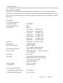
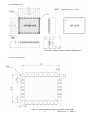
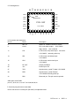
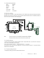
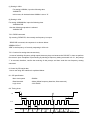
PROGRAMABLE OSCILLATOR MODEL PCK3GF-1 USER’S MANUAL DIGITAL SIGNAL TECNOLOGY, INC. 1-7-30, HlGASHI BENZAl, ASAKA CITY SAITAMA 351-0022, JAPAN TEL: 81-48-468-6094 FAX: 81-48-468-6210 e-mali:[email protected] http://www.dst.co.jp/en CONTENTS 1. General Description……………………… 3 2. Specification………………………………. 3 3. Outer Dimension………………………….. 5 4. Recommended Pad………………………..5 5. Pin Assignment……………………………..6 6. Pin names and description………………..6 7. Control by Asynchronous serial data…….6 8. Control by SPI serial data…………………8 9. Shipping inspection……………………...…9 10. Soldering Conditions………………………9 11. Warranty……………………………………9 12. Others……………………………………….9 2 DST 2012-7-11 REV1.2 1. General Description As a signal source, desired clock signals can be generated with 1KHz resolution in an extremely wide band of 50MHz to 3000MHz. The frequency is set with asynchronous serial data. Also, the frequency can be set by SPI serial data. Once frequency is successfully set, the frequency is automatically memorized into EEPROM. At the next power on, the last entered frequency is retrieved. Frequency stability and accuracy depends on external clock source. 2. Specification 2-1. Electrical Specification 1) Frequency Range 50~3000MHz 2) Frequency Resolution 1KHz 3) Phase Noise @3GHz 10 Hz offset : -55 dBc/Hz Typ. 100 Hz offset : -85 dBc/Hz Typ. 1 kHz offset : -104 dBc/Hz Typ. 10 kHz offset : -105 dBc/Hz Typ. 100 kHz offset : -105 dBc/Hz Typ. 1MHz offset : -132 dBc/Hz Typ. 10MHz offset -155 dBc/Hz Typ. 4) Spurious -65 dBc Max (except harmonics) 5) Output Level >+3dBm @50ohm 6) Ext Ref Requirement 50MHz or 100MHz Level : +6dBm~+10dBm @1k ohm 7) Ext Ref Input Impedance 1Kohm//5pf sine or square wave 8) Unlock Output Locked: High Level Unlocked: Low Level 3.3V CMOS Level 9) Lock Time 40m sec Max 10) Controls (1) Asynchronous Serial Communication 9600bps, 8bits, one stop bits, non-parity (2) SPI serial communication 3 bytes data (24bits) 11) Power Supply +5V+/-5% 500mA 12)Dimensions 20.3x25.4x7.6mm 2-2. Environmental Condition 1)Operating Temperature Range 0 to +60 Deg. C 2)Storage Temperature Range -30 to +70 Deg. C 3 DST 2012-7-11 REV1.2 2-3. Phase noise performance 4 DST 2012-7-11 REV1.2 3. Outer Dimension CAUTION:Bottom surface is resisted GND pattern. 4. Recommended Pad Note: It is recommended to restrict any pattern except GND. 5 DST 2012-7-11 REV1.2 GND 7 23 GND 22 GND 21 GND 20 GND 19 GND GND RSV GND RXD GND TXD GND +5V GND 31 30 29 28 27 26 25 24 18 RF OUT 17 GND GND 16 6 CLK 15 RF IN TOP VIEW GND 14 5 13 GND PCK-3GF SDI 4 GND 12 GND /CS 11 3 GND 10 GND PIN1 MARKING 9 2 LOCK GND 8 1 GND GND 32 5. Pin Assignment 6. Pin names and description Pin No. Name Description 6 REF IN 50MHz or 100MHz reference 1Kohm 9 LOCK PLL Lock status output High: locked 11 /CS 3.3V CMOS low: unlocked In SPI mode, chip select input low active. 3.3V CMOS Internally pulled up 13 SDI In SPI mode, serial data input. 3.3V CMOS 15 CLK In SPI mode, serial clock input. 3.3V CMOS 18 RF OUT Output pin,50ohm 25 +5V Power input +5V 27 TXD Asynchronous_serial TX data 3.3V CMOS 29 RXD Asynchronous_serial RX data 3.3V CMOS Internally pulled up 31 RSV Reserved pin. This pin must be opened. Other pins are all GND pin1-5,7,8,10,10,12,14,16,17,19-24,26,28,30,32. 7. Control by Asynchronous serial data How to set from a PC serial port (RS-232C) is explained below. 6 DST 2012-7-11 REV1.2 7-1. Communication specification Speed 9600bps Data bits 8 bits Stop bits 1 bit Parity None Flow Control None Logic Level 3.3V CMOS 7-2. RS-232C connection The logic level of PCK3GF-1 serial communication is 3.3V CMOS, which cannot be directly connected to RS-232C level such as PC serial port. Level conversion between RS-232C and 3.3V CMOS are made via the level convertor as shown in the following figure. +3.3V GND +5V GND TXD GND RXD GND GND RSV +5V GND GND GND GND GND GND GND 1μ/50V + 15 VGND GND PCK-3GF RF IN 6 GND TOP VIEW GND 10MHz 16 VCC RF OUT GND 1μ/50V 2 V+ 1 C1+ 3 C14 C2+ 5 C2- 12 13 11 14 GND CLK GND SDI ICL323CP GND /CS GND Lock GND GND + + 1μ/50V + TO COMPUTER 1μ/50V RS-232C PORT 2 TXD 3 RXD 7 5 6 CTS DSR 8 20 DTR D-SUB 25PIN Note: The level convertor IC is ICL3232CP manufactured by INTERSIL. The other ICL32xx series of level convertor ICs are also used. 7-3. Command definitions Character strings enclosed in double quotation marks “”means ASCII code,and CR and LF, which are control codes, means 0D(hex) and 0A (hex). If any invalid command is entered, ”INVALID DATA”CR LF “*” is returned. All characters used for input should be uppercase. If a normal command is entered,”*” is returned. Also the entered data is echoed back. 7-3-1. Frequency setting command For frequency setting, input can be made in MHz, KHz unit. 7 DST 2012-7-11 REV1.2 (1) Setting in MHz For setting 2450MHz, input the following data. “2456M”CR In this case, all the data below 100KHz is set to “0”. (2) Setting in KHz For setting 2450002KHz, input the following data. “2456002K”CR Also the following expression is allowed. “2456002”CR 7-3-2. READ command By entering “READ”CR, the currently set frequency is output. “READ”CR is entered, the response is as shown below. “ffffffffKHz”CR LF “fffffff” is the frequency of currently outputting in KHz unit. 7-3-3. Caution for setting data consecutively In case of switching frequency at high speed, data may drop out because the PCK3GF-1 does not perform flow control. Upon completion of processing by sending a frequency setting command in 6-3-1, the prompt “*” is returned; therefore, confirm the receiving of this prompt, and then send the next frequency setting command. 8. Control by SPI serial data How to set using SPI interface is explained below. 8-1. SPI specification Max. clock speed 500KHz Data bits width 24bits (22bits frequency data bits, 2bits reserved ) Logic Level 3.3V CMOS 8-2. Timing chart t1 /CS t2 t5 CLK t4 t3 SDI D23 D22 D21 D20 D19 D18 8 D19 D2 D1 D0 DST 2012-7-11 REV1.2 Timing characteristic Parameter Condition Min. Unit t1 CLK setup time to /CS 50 ns t2 CLK period 2 us t3 SDI setup time to CLK rise edge 100 ns t4 SDI hold time to CLK rise edge 100 ns t5 /CS set up time to CLK rise edge 50 ns 8-3. Command definitions 24bits frequency data is transferred bye SPI. Actual frequency data bits are 21bits among 24 bits, the remaining 3bits are not used. Bit definition is as follows. Bits Name Width Description bit [23:22] Reserved 2 bits Not used, do not care bit [21:0] Frequency 22 bits Frequency data in 1KHz resolution in binary. For example, if you set 2456000KHz, frequency data of KHz unit must be converted to binary data. 2456000KHz is converted to 2579C0 hex in 22 bits binary data. 9. Shipping inspection 100%inspection shall be performed for the electrical specification in 2-1. 10. Soldering Conditions Peak Temperature: 240degC Soldering time: Less than 10 second at the peak temperature. 11. Warranty If any defect is found due to the manufacture’s improper production or design within one year after delivery, repair or replacement shall be performed at the manufacturer’s responsibility. DS Technology, Inc assumes no liability for damages that may occur as a result of handling by users even though the warranty period. 12. Others 12-1. This product, which employs a CMOS device, may be easily damaged by static electricity. DS Technology, Inc assumes no liability for damages that may occur as the result of handling by users even though the above warranty period. 12-2. Do not supply over voltage power supply, module may be damaged. DS Technology, Inc assumes no liability for damages that may occur as the result of handling by users even though the above warranty period. Descriptions of this manual are subject to change without notice. No portion of this manual can be reproduced without the permission of DS Technology, Inc. The contents of this manual do not apply to the warranty in executing an industrial property or other rights, nor permission for the right 9 DST 2012-7-11 REV1.2 of execution. DS Technology Inc assumes no responsibility for the third party’s industrial property accrued from using the circuits descried in this manual.