1
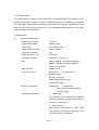
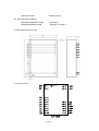
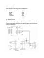
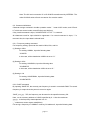
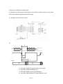
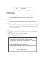
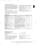
PCL-130F User’s Manual
Digital Signal Technology Inc.
1-7-30, Higashi Benzai, Asaka, Saitama, 351-0022, Japan
TEL 81-48-468-6094
FAX 81-48-468-6210
Mail :
[email protected]
URL :
http://www.dst.co.jp/en
page 1
1. Functional outline
As a signal source, desired clock signals can be generated with 1Hz resolution in an
extremely wide band of 1MHz to 130MHz. Wideband signals up to 130MHz are generated
by a 48-bit DDS (direct digital synthesizer). The frequency is set with asynchronous serial
data. Also, the frequency which is saved in the incorporated 120CH memory can be easily
set by selecting the parallel data.
2. Specifications
2-1.
Electrical specifications
Power supply voltage
+3.3V±5%
Current consumption
700mA or less
Output level
3.3V CMOS LEVEL
Output frequency range
1MHz - 130MHz
Frequency resolution
1Hz
Output waveform duty
50%±20%
Frequency accuracy
±20ppm(0 – 50 deg. C)
Jitter
10MHz - 50MHz less than ±250pSrms
50MHz - 130MHz less than ±30pSrms
(Cycle to Cycle Jitter)
Spurious level
-45dB or more
Frequency control
Serial input
two signal lines
9600bps, 8 bits
No parity, 1 stop bit
ASCII 9-digit numerical data +
delimiter (CR code)
Memory CH selection
Parallel input
8 signal lines
7 bits; selection signals (120CH)
1 bit; SET signal
Frequency setting time
* Within 4mS
(time between end of transferring a delimiter
code and obtaining the desired frequency in
the case of serial data. )
* Within 350uS
(time between falling edge of
SET signal
and obtaining the desired frequency in the
case of memory CH selection.)
page 2
Outer dimensions
50x35x12 (mm)
2-2. Environmental conditions
Operating temperature range
0~50 deg.C
Storage temperature range
-30 deg C~+70 deg. C
3. Outline dimensions (in mm)
4. Pin assignments
GND
1
NC
2
D0
D1
D2
D3
D4
D5
D6
SET
PIN1
3
4
5
6
7
8
9
10
18
GND
17
OUT
16
15
14
TXD
RXD
+3.3V
+3.3V
GND
GND
13
12
11
(TOP VIEW)
page 3
5. Pin names and descriptions
Pin No.
Name
Description
1
GND
Power supply/signal GND.
2
NC
Not used
3
D0
Memory CH selection signal input.
Signal selection bit 0 (20).
4
D1
Memory CH selection signal input.
Signal selection bit 1 (21).
5
D2
Memory CH selection signal input.
Signal selection bit 2 (22).
6
D3
Memory CH selection signal input.
Signal selection bit 3 (23).
7
D4
Memory CH selection signal input.
Signal selection bit 4 (24).
8
D5
Memory CH selection signal input.
Signal selection bit 5 (25).
9
D6
Memory CH selection signal input
Signal selection bit 6(26)
10
SET
Set signal input for memory CH selection.
As it is pulled up internally, the frequency in the memory CH
selected by D0 – D6 is set by connecting it to GND.
Data is loaded on the falling edge.
11
GND
Power supply/signal GND.
12
GND
Power supply/signal GND.
13
+3.3V
Power supply. Supply +3.3V +/-5%.
14
-3.3V
Power supply. Supply +3.3V +/-5%.
15
RXD
Asynchronous serial data input pin.
The level is 3.3V CMOS.
When not in use, open it.
16
TXD
Asynchronous serial data output pin.
The level is 3.3V CMOS.
When not in use, open it.
17
OUT
Signal output pin.
The level is 3.3V CMOS.
18
GND
Power supply/signal GND
page 4
6. Control by serial data
How to set from a PC serial port (RS-232C) is explained below.
6-1. Communication specifications
Communication speed
9600bps
Data bit
8 bits
Parity
None
Stop bit
1 bit
Flow control
None
Level
3.3V CMOS
6-2. RS-232C connection
The electric signal level of PCL-130 serial communications is 3.3V CMOS, which cannot be
directly connected to a PC serial port, etc. (RS-232C level).
Level conversions between RS-232C and 3.3V CMOS are made via the level converter as
shown in the following figure.
page 5
Note: The U2 level conversion IC is ICL3232CP manufactured by INTERSIL. The
other ICL32XX series of level conversion ICs are also usable.
6-3. Command definitions
Character strings enclosed in double quotation marks “ ” mean ASCII codes, and CR and
LF, which are control codes, mean 0D (hex) and 0A (hex).
If any invalid command is input, “INVALID DATA” LF CR “*” is returned.
All characters used for input should be uppercase. If a normal command is input, “*” is
returned. Also, the input data is echoed back.
6-3-1. Frequency setting command
For frequency setting, inputs can be made in MHz, KHz, and Hz.
(1) Setting in MHz
For setting 123MHz, input the following data.
“123M”CR
In this case, all the data below 100KHz is set to “0.”
(2) Setting in KHz
For setting 123456KHz, input the following data.
“123456K”CR
In this case, all the data below 100Hz is set to “0.”
(3) Setting in Hz
For setting 123456789Hz, input the following data.
“123456789”CR
6-3-2. SAVE command
By inputting “SAVE”CR, the currently set frequency is saved in nonvolatile RAM. The saved
frequency is output when the power is turned on again.
“SAVE_xxx_yyy...”CR, the frequency can be saved in the specified memory CH.
Here, xxx is a memory address of 120CH specified by 0 - 119 at the maximum.
yyyyyy... is the frequency data explained in 6-3-1.
“_” underscore means sapce code(20hex)
For saving a frequency of 123MHz in memory CH address 0, input the following data.
page 6
“SAVE_0_123M”CR
For saving a frequency of 123456KHz in memory CH address 119, input the following data.
“SAVE_119_123456K”CR
6-3-3. READ command
By inputting “READ”CR, the currently saved data in all memory CHs is output. The
response is as follows:
“fffffffff” CR LF
“000_fffffffff” CR LF
“001_fffffffff” CR LF
“002_fffffffff” CR LF
.
.
.
“119_fffffffff” CR LF
“*”
“fffffffff” on the first line is the default frequency to be output at power-on. On the second line
to the 121st line frequency data is saved in the memory CHs.
Here, “fffffffff” is the output frequency in each memory CH displayed in Hz.
“_” underscore means space code(20hex)
6-4. Caution for setting data consecutively
In the case of sending data consecutively, data may drop out because the PCL130 does
not perform flow control. Upon completion of processing by received frequency command
in 6-3-1, the prompt “*” is returned, therefore, confirm the receiving of this prompt, and then
send the next frequency setting command.
page 7
7. Memory CH selection by parallel data
It is designed so that frequency data saved in the maximum 120CH memory can be easily
set by seven selection signals and one SET signal.
7-1. Example of SW connection circuit
7-2
t2
D0一D6
SET
t1
t3
t4
出力周波数
f1
f2
t1 : more than 560nS SET signal minimum pulse width
t2 : more than 120nS data holding time
t3 : more than 350uS Frequency switching time
t4 : more than 400uS shortest SET signal repetition cycle
page 8
Remarks: D0-D6 and SET signal is pulled up internally.
H : open
L : short to GND
The input data of D0-D6 is loaded on the falling edge of SET.
8. Shipping inspection
8-1. Electrical inspection
100% inspection shall be performed for the electrical specifications in 2-1.
8-2. Appearance inspection
Inspection shall be performed for contamination and bends in pins.
9. Soldering conditions
Perform soldering at a temperature of 260 deg. C or less within 10 seconds.
10. Warranty
If any defect is found due to the manufacturer’s improper production or design
within one year after delivery, repair or replacement shall be performed at the
manufacturer’s responsibility.
11. Other
11-1. This product, which employs a CMOS device, may be easily damaged by static
electricity.
11-2. Keep in mind that immersion cleaning is not allowed.
11-3. Special humidity control is not necessary.
・ Descriptions in this manual are subject to change without notice.
・ No part of this manual may be reproduced without our permission.
・ We shall assume no liability for any user damage as a result of an
accident, etc.
・ Descriptions in this manual shall not guarantee the practice of industrial
property and other rights or grant a license for them.
・ We shall assume no liability for any third party’s industrial property rights
attributable to the use of circuits, etc., described in this manual.
Digital Signal Technology, Inc.
page 9