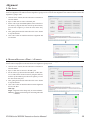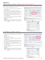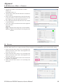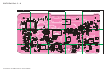
1
Vertex Standard LMR, Inc. VHF FM Transceiver VX-230 4-8-8 Nakameguro, Meguro-Ku, Tokyo 153-8644, Japan Series ©2012 Vertex Standard LMR, Inc. EC085N90I Service Manual Introduction This manual provides technical information necessary for servicing the VX-230 FM Transceiver. Servicing this equipment requires expertise in handling surface-mount chip components. Attempts by non-qualified persons to service this equipment may result in permanent damage not covered by the warranty, and may be illegal in some countries. Two PCB layout diagrams are provided for each double-sided circuit board in the transceiver. Each side of is referred to by the type of the majority of components installed on that side (“leaded” or “chip-only”). In most cases one side has only chip components, and the other has either a mixture of both chip and leaded components (trimmers, coils, electrolytic capacitors, ICs, etc.), or leaded components only. While we believe the technical information in this manual to be correct, VERTEX STANDARD assumes no liability for damage that may occur as a result of typographical or other errors that may be present. Your cooperation in pointing out any inconsistencies in the technical information would be appreciated. Important Note This transceiver was assembled using Pb (lead) free solder, based on the RoHS specification. Only lead-free solder (Alloy Composition: Sn-3.0Ag-0.5Cu) should be used for repairs performed on this apparatus. The solder stated above utilizes the alloy composition required for compliance with the lead-free specification, and any solder with the above alloy composition may be used. Contents Specifications........................................................... 2 Exploded View & Miscellaneous Parts .................3 Parts List .................................................................4 Block Diagram ........................................................ 5 Circuit Description ................................................ 6 Alignment ................................................................8 VX-230 Series VHF FM Transceiver Service Manual MAIN Unit (Lot. 1 ~ 4) ........................................ MAIN Unit (Lot. 5 ~ 7) ........................................ MAIN Unit (Lot. 8 ~ 44) ...................................... MAIN Unit (Lot. 45 ~ 50) .................................... MAIN Unit (Lot. 51 ~) ......................................... 15 18 21 24 27 1 Specifications VTX/EXP version General 134 -174 MHz 16 7.4 V DC ±10 % 12.5 / 20 / 25 kHz 9.0 hrs (7.3 hrs w/o saver) w/FNB-V103LI (1150 mAh) 16.5 hrs (13.5 hrs w/o saver) w/FNB-V104LI (2000 mAh) Operating Temperature Range: –22 °F to +140 °F (–30 °C to +60 °C) Frequency Stability: ±2.5 ppm RF Input-Output Impedance: 50 Ohm Dimension (W x H x D): 2.3” x 4.3” x 1.2” (58 x 110 x 30 mm) Weight (Approx.): 10.1 oz ( 285 g) w/FNB-V103LI, Antenna, Belt Clip Frequency Range: Number of Channels: Power Supply Voltage: Channel Spacing: Battery Life (5-5-90 duty): Receiver (measured by TIA/EIA-603) Sensitivity (12dB SINAD): Adjacent Channel Selectivity: Intermodulation: Spurious and Image Rejection: Audio Output: 0.25 μV typical 65 / 60 dB (25 kHz / 12.5 kHz) 65 / 60 dB (25 kHz / 12.5 kHz) 65 dB 500 mW @ 4 ohms 5 % THD Transmitter (measured by TIA/EIA-603) Output Power: Modulation: Conducted Spurious Emission: FM Hum & Noise: Audio Distortion: CE version General Frequency Range: Number of Channels: Power Supply Voltage: Channel Spacing: Battery Life (5-5-90 duty): Temperature Range: Frequency Stability: RF Input-Output Impedance: Battery Pack: Dimension (W x H x D): Weight (Approx.): 5/1W 16K0F3E, 11K0F3E 65 dB below carrier 45 / 40 dB (25 kHz / 12.5 kHz) < 3 % @1 kHz 134MHz - 174MHz (VX-231-ED0B-5) 16 7.4 V DC ±10 % 12.5 / 20 / 25 kHz 9 hrs (7.3 hrs w/o saver) w/FNB-V103LI (1150 mAh) 16.5 hours (13.5 hrs w/o saver) w/FNB-V104LI (2000 mAh) –20 °C to +55 °C (Operation) –0 °C to +45 °C (Battery Charging) Turn the radio off while charging the battery, and use only the Vertex Standard Co., Ltd. Model PA-42C/U AC Adapter and CD-34 Desktop. ±2.5 ppm 50 Ohm FNB-V103LI / FNB-V104LI Risk of explosion if battery is replaced by an incorrect type. Dispose of used batteries according to the instructions. 58 x 110 x 30 mm 285 g w/FNB-V103LI, Antenna, Belt Clip Receiver (Measurement per EN 300 086) Sensitivity (20 dB SINAD): Adjacent Channel Selectivity: Intermodulation: Spurious and Image Rejection: FM Noise: Spurious Emission: Audio Output: 0.5 μV 70 / 60 dB (25 kHz / 12.5 kHz) 65 dB 70 dB 45 / 40 dB (25 kHz / 12.5 kHz) –36 dBm (<1GHz), –30 dBm (>1GHz) 500 mW @ 4 ohms 5 % THD Transmitter (Measurement per EN 300 08) Output Power: 5/1W Modulation: Variable Reactance Modulation Maximum Frequency Deviation: ±2.5 / ±4.0 / ±5.0 kHz (12.5 kHz / 20 kHz / 25 kHz) FM Hum & Noise: 45 / 40 dB (25 kHz / 12.5 kHz) Audio Distortion: < 5 % @1 kHz Spurious Emission: –36 dBm (<1GHz), –30 dBm (>1GHz) Specification may be changed without notification. VX-230 Series VHF FM Transceiver Service Manual 2 Exploded View & Miscellaneous Parts RA1096000 COIL SPRING RA0173500 CAP (MIC/SP) CS2121102 FRONT CASE ASSY RA1058900 O RING RA1355400 RELEASE KNOB RA090600D KNOB (VOL) RA1107500 LATCH PLATE RA091760D KNOB ASSY (CH) RA104190C FRAME (PTT) RA090490C COVER (PTT) RA1041800 RUBBER (SIDE) RA104170A RUBBER (PTT) RA0187600 SHEET RA1042100 LOCK PLATE T9318325 WIRE ASSY (YEL 65) RA0557900 SP NET T9318324 WIRE ASSY(BLK 65) M4090192B SPEAKER (4-ohm/1W) RA1085300 TAPE (SP) RA1124300 SHIELD CASE COVER MAIN ASSY CS2010406 RA011020A HOLDER RUBBER (MIC) RA090590A NUT RA103890B RUBBER PACKING RA090590A NUT RA0248200 GROUND PLATE RA103910A TERMINAL ASSY RA0248200 GROUND PLATE RA037690B SHEET CP9379001 REAR CASE ASSY RA1039000 PACKING PAD (BATT-C) RA103880B CASE COVER (REAR) BATTERY PACK AAF60X101 CLIP-18 REF VXSTD P/N RA1424600 U20206007 U24110002 U44105001 U24106001 U07230302 DESCRIPTION QTY. SCREW SM3X8SUS 1 BINDING HEAD SCREW M2.6X6B 2 BIND HEAD TAPTITE-B M2X10NI 2 PAN HEAD TAPTITE-B M2X5 11 BIND HEAD TAPTITE-B M2X6 2 PAN HEAD SCREW M2X3NI #3 1 Non-designated parts are available only as part of a designated assembly. VX-230 Series VHF FM Transceiver Service Manual 3 Parts List REF. DESCRIPTION CD1001 CF1001 F 1001 MC1001 Q 1010 S 1001 S 1002 S 1003 S 1004 VR1001 X 1001 X 1002 XF1001 PCB with Components FRONT CASE ASSY REAR CASE ASSY TERMINAL ASSY CASE COVER KNOB KNOB ASSY NUT RUBBER PACKING PACKING PAD HOLDER RUBBER SCREW BINDING HEAD SCREW BIND HEAD TAPTITE-B PAN HEAD TAPTITE-B BIND HEAD TAPTITE-B PAN HEAD SCREW SPEAKER CERAMIC DISC CERAMIC FILTER CHIP FUSE MIC. ELEMENT FET TACT SWITCH TACT SWITCH TACT SWITCH ROTARY SWITCH POT. XTAL U3B TCXO XTAL FILTER VALUE (1 pc) (2 pcs) (2 pcs) (11 pcs) (2 pcs) (1 pc) 4-ohm 3.15A 3.6864MHz 16.8MHz V/W TOL. MFR’S DESIG VXSTD P/N CS2010406 CS2121102 CP9379001 RA103910A REAR RA103880B VOL RA090600D CH RA091760D RA090590A RA103890B BATT-C RA1039000 MIC RA011020A SM3X8SUS RA1424600 M2.6X6B U20206007 M2X10NI U24110002 M2X5 U44105001 M2X6 U24106001 M2X3NI #3 U07230302 A-S0000036-004 4-OHM/1W M4090192B JTBM450CX24 H7901530 LTM450FW-A H3900572A FHC16 322ADTP Q0000118 PF0-1055P M3290045 RQA0011DNS G3070392 SKHLLD N5090066 SKRTLAE010 N5090130 SKRTLAE010 N5090130 ED10304O-FB15S7.0-A16-100 N0190195 RK0971111 20KA/SW J60800256 3.686400MHz (11p) H0103307 TTS14VSB-A3 16.80MHZ H9501100 MFT67N2 67.650MHZ H1102473 VX-230 Series VHF FM Transceiver Service Manual VERS. LOT. SIDE LAY ADR B A A A A B B B B B B B B c3 A2 B1 C2 B2 c1 c2 c3 b1 a1 c4 b4 b3 4 Block Diagram VX-230 Series VHF FM Transceiver Service Manual 5 Circuit Description 1. Circuit Configuration by Frequency The receiver is a Double-conversion Super-heterodyne with a first intermediate frequency (IF) of 67.65MHz and a second IF of 450kHz. Incoming signal from the antenna is mixed with the local signal from the VCO/PLL to produce the first IF of 67.65MHz. This is then mixed with the 67.2MHz second local oscillator output to produce the 450kHz second IF. This is detected to give the demodulated signal. The transmit signal frequency is generated by the PLL VCO, and modulated by the signal from the microphone. It is then amplified and sent to the antenna. 2. Receiver System 2-1. Front-end RF amplifier Incoming RF signal from the antenna is delivered to the RF Unit and passes through Low-pass filer, antenna switching diode, high pass filter and removed undesired frequencies by varactor diode (tuned band-pass filer). The passed signal is amplified in Q1013 (2SC5006) and moreover cuts an image frequency with the tuned band pass filter and comes into the 1st mixer. 2-2. First Mixer The 1st mixer consists of the Q1024 (3SK293). Buffered output from the VCO is amplified by Q1027 (2SC5005) to provide a pure first local signal between 201.65 and 241.65MHz for injection to the first mixer. The IF signal then passes through monolithic crystal filters XF1001(±7.5 kHz BW) to strip away all but the desired signal. 2-3. IF Amplifier The first IF signal is amplified by Q1033 (2SC4215Y). The amplified first IF signal is applied to FM IF subsystem IC Q1038 (NJM2591V) which contains the second mixer, second local oscillator, limiter amplifier, noise amplifier, and RSSI amplifier. The signal from reference oscillator X1002 becomes 4 times of frequencies in Q1038, it is mixed with the IF signal and becomes 450kHz. The second IF then passes through the ceramic filter CF1001 (LTM450FW) to strip away unwanted mixer products, and is applied to the limiter amplifier in Q1038, which removes amplitude variations in the 450kHz IF, before detection of the speech by the ceramic discriminator CD1001 (TBM450CX24). 2-4. Audio amplifier Detected signal from Q1038 is inputted to TX/RX switch Q1001-4 (TC74VHC4066AFT). The signal which appeared from Q1001 is in high pass filter Q1050 (NJM12902). The signal which passed Q1050 goes to AF volume (VR1001). And then the signal goes to audio amplifier Q1005 (NJM2070M). The output signal from Q1005 is in audio speaker. VX-230 Series VHF FM Transceiver Service Manual 2-5. Squelch Circuit There are 16 levels of squelch setting from 0 to 15. The level 0 means open the squelch. The level 1 means the threshold setting level and level 14 means tight squelch. From 2 to 13 is established in the middle of threshold and tight. The bigger figure is nearer the tight setting. The level 15 becomes setting of carrier squelch. 2-5-1. Noise Squelch Noise squelch circuit is composed of the band path filter of Q1038, and noise detector D1029 (1SS400G). When a carrier isn't received, the noise ingredient which goes out of the demodulator Q1038 is amplified in Q1038 through the band path filter Q1038, is detected to DC voltage with D1029 and is inputted to 52pin (the A/D port) of the Q1026 (CPU). When a carrier is received, the DC voltage becomes low because the noise is compressed. When the detected voltage to CPU is high, the CPU stops AF output with Q1001-3 “OFF” by making the 41pin (CPU) “L” level. When the detection voltage is low, the CPU makes Q1001 ON with making 41pin “H” and the AF signal is output. 2-5-2. Carrier Squelch The CPU (53pin: A/D port) detect RSSI voltage output from Q1038 12 pin, and controls AF output. The RSSI output voltage changes according to the signal strength of carrier. The stronger signal makes the RSSI voltage to be higher voltage. The process of the AF signal control is same as Noise Squelch The shipping data is adjusted -1dBu (EMF) higher than squelch tight sensitivity. 3. Transmitter System 3-1. Mic Amplifier The AF signal from internal microphone MC1001 or external microphone J1002 is amplified with microphone amplifier Q1049-3 (NJM12902V). This signal enters high pass filter Q1050 via the mute switch Q1001-1(TC74VHC4066AFT). Afterwards, the switch circuit is controlled in the gain by way of microphone gain volume Q1012 (M62364FP-CH1). AF signal is passes a pre-emphasis circuit and is input to the limiter amplifier Q1049-2 (NJM12902V). The signal passed splatter filter of Q1049 and adder amplifier Q1046 is adjusted by maximum deviation adjustment volume Q1012 (M62364FP-CH4). The AF signal ingredient is amplified Q1046(NJM12902V). After that, it is made FM modulation to transmit carrier by the modulator D1014 (HVC383B) of VCO. 6 Circuit Description 3-2. Drive and Final amplifier The modulated signal from the VCO Q1032 (2SC4227) is buffered by Q1027 (2SC5005). Then the signal is buffered by Q1018 (2SC5227) for the final amplifier driver Q1015 (RQA0004PXDQS). The low-level transmit signal is then applied to Q1010 (RQA0011DNS) for final amplification up to 5watts output power. The transmit signal then passes through the antenna switch D1002 (RLS135) and is low pass filtered to suppress away harmonic spurious radiation before delivery to the antenna. 3-3. Automatic Transmit Power Control The current detector Q1052-1 (NJM12904R) detects the current of Q1010 and Q1015, and converts the current difference to the voltage difference. The output from the current detector Q1052-1 is compared with the reference voltage and amplified by the power control amplifier Q1052-2. The output from Q1052-2 controls the gate bias of the final amplifiers Q1010 and the final amplifier driver Q1015. The reference voltage changes into four values (Transmit Power High and Low) controlled by Q1012 (M62364FP-CH8). 4-3. PLL The PLL IC consists of reference divider, main divider, phase detector, charge pumps and pulse swallow operation. The reference frequency from TCXO is inputted to 1pin of PLL IC and is divided by reference divider. The other hand, inputted feed back signal to 8pin of PLL IC from VCO is divided with the dividing ratio which becomes same frequency as the output of reference divider. These two signals are compared by phase detector, the phase difference pulse is generated. The phase difference pulse and the pulse from through the charge pumps and LPF. It becomes the DC voltage to control the VCO. The oscillation frequency of VCO is locked by the control of this DC voltage. The PLL serial data from CPU is sent with three lines of SDO (60pin), SCK (58pin) and PSTB (59pin). The lock condition of PLL is output from the UL (14Pin) terminal and UL becomes “H” at the time of the lock condition and becomes “L” at the time of the unlocked condition. The CPU always watches over the UL condition, and when it becomes “L” unlocked condition, the CPU prohibits transmitting and receiving. 4. PLL Frequency Synthesizer The frequency synthesizer consists of PLL IC, Q1042 (MB15E03SL), VCO, TCXO (X1002) and buffer amplifier. The output frequency from TCXO is 16.8MHz and the tolerance is ±2.5 ppm (in the temperature range -30 to +60 degrees). 4-1. VCO While the radio is receiving, the RX oscillator Q1030 (2SK508) in VCO generates a programmed frequency between 201.65 and 241.65MHz as 1st local signal. While the radio is transmitting, the TX oscillator Q1032 (2SC4227) in VCO generates a frequency between 134 and 174MHz. The output from oscillator is amplified by buffer amplifier Q1027 (2SC5005) and becomes output of VCO. The output from VCO is divided, one is amplified by Q1027 and feed back to the PLL IC 8pin. It is put into the mixer as the 1st local signal through D1012, in transmission, it is buffered Q1018, and more amplified in Q1015 through D1012 and it is put into the final amplifier Q1010. 4-2. VCO Tuning Voltage Tuning voltage of VCO is expanding the lock range of VCO by controlling the cathode of varactor diode at the voltage and the control voltage from PLL IC. VX-230 Series VHF FM Transceiver Service Manual 7 Alignment Introduction Required Test Equipment The VX-230 series has been aligned at the factory for the specified performance across the entire frequency range specified. Realignment should therefore not be necessary except in the event of a component failure. All component replacement and service should be performed only by an authorized Vertex Standard representative, or the warranty policy may be voided. The following procedures cover the sometimes critical and tedious adjustments that are not normally required once the transceiver has left the factory. However, if damage occurs and some parts are replaced, realignment may be required. If a sudden problem occurs during normal operation, it is likely due to component failure; realignment should not be done until after the faulty component has been replaced. We recommend that servicing be performed only by authorized Vertex Standard service technicians who are experienced with the circuitry and fully equipped for repair and alignment. Therefore, if a fault is suspected, contact the dealer from whom the transceiver was purchased for instructions regarding repair. Authorized Vertex Standard service technicians realign all circuits and make complete performance checks to ensure compliance with factory specifications after replacing any faulty components. Those who do undertake any of the following alignments are cautioned to proceed at their own risk. Problems caused by unauthorized attempts at realignment are not covered by the warranty policy. Also, Vertex Standard must reserve the right to change circuits and alignment procedures in the interest of improved performance, without notifying owners. Under no circumstances should any alignment be attempted unless the normal function and operation of the transceiver are clearly understood, the cause of the malfunction has been clearly pinpointed and any faulty components replaced, and the need for realignment determined to be absolutely necessary. The following test equipment (and thorough familiarity with its correct use) is necessary for complete realignment. Correction of problems caused by misalignment resulting from use of improper test equipment is not covered under the warranty policy. While most steps do not require all of the equipment listed, the interactions of some adjustments may require that more complex adjustments be performed afterwards. Do not attempt to perform only a single step unless it is clearly isolated electrically from all other steps. Have all test equipment ready before beginning, and follow all of the steps in a section in the order presented. VX-230 Series VHF FM Transceiver Service Manual Radio Tester with calibrated output level at 200 MHz In-line Wattmeter with 5% accuracy at 200 MHz 50-ohm, 10-W RF Dummy Load Regulated DC Power Supply (standard 7.5 VDC, 2 A) Frequency Counter: ±0.2 ppm accuracy at 200 MHz AF Signal Generator AC Voltmeter DC Voltmeter VHF Sampling Coupler Microsoft® Windows® 2000, XP or Vista Micorosoft® Net Framework 2.0 or later Vertex Standard CE99 Alignment program and CT-42 Connection Cable or FIF-12 USB Programming Interface and CT-106 PC Programming Cable. Alignment Preparation & Precautions A 50-ohm RF Dummy load and in-line wattmeter must be connected to the main antenna jack in all procedures that call for transmission, except where specified otherwise. Correct alignment is not possible with an antenna. After completing one step, read the following step to determine whether the same test equipment will be required. If not, remove the test equipment (except dummy load and wattmeter, if connected) before proceeding. Correct alignment requires that the ambient temperature be the same as that of the transceiver and test equipment, and that this temperature be held constant between 20 °C and 30 °C (68 °F ~ 86 °F). When the transceiver is brought into the shop from hot or cold air, it should be allowed time to come to room temperature before alignment. Whenever possible, alignments should be made with oscillator shields and circuit boards firmly affixed in place. Also, the test equipment must be thoroughly warmed up before beginning. Note: Signal levels in dB referred to in this procedure are based on 0 dBμ EMF = 1.0 μV. 8 Alignment Test Setup Basic Alignment Mode Setup the test equipment as shown for transceiver alignment, then apply 7.5 V DC power to the transceiver. In the Basic Alignment mode, the aligned data written in the radio will be able to re-align its alignment data. In this mode, there are many items to align with five points (F1, F2, F3, F4, F5) except “Frequency”, “Mic Sense”, “SQL/RSSI”, and “Battery”. The value of each parameter can be changed to desired position by “” / “” arrow key for up/down, direct number input and drag the mouse. 50-ohm Dummy Load RF Signal Generator RF Sampling Coupler Inline Wattmeter ANT Transceiver MIC/SP Deviation Meter BATTERY TERMINAL Power Supply 7.5 VDC CT-42 or FIF-12 + CT-106 Frequency Counter COM Port (for CT-42) or USB Port (for FIF-12 + CT-106) CLONE SP GND SP MIC MIC CLONE GND The Alignment Tool Outline Installation the tool Install the CE99 (Clone Editor) to your PC. “Basic Alingment” function in the “Radio” menu of CE99. Action of the switches When the transceiver is in alignment mode, the action of PTT and KEY is ignored. All of the action is remote controlled by PC. To enter the Basic Alignment Mode, select “Basic Alignment” in the main menu “Radio”. It will start to “Read” the written personalized data from the radio. Then pressing the button “OK” will start the Basic Alignment Mode. Note: when all items are aligned, it is strongly recommended to align according to following order. The detail information is written in the help of CE99 (Clone Editor). 1. PLL Reference Frequency (Frequency) 2. RX Sensitivity (RX Tune) 3. Squelch (SQL/RSSI) 4. TX Power <High> / <Low> 5. Mic Sense 6. Maximum Deviation <Wide> / <Narrow> 7. Modulation Balance <Wide> / <Narrow> 8. CTCSS Deviation <Wide> / <Narrow> 9. DCS Deviation <Wide> / <Narrow> 10. Battery Unit During alignment, you may select the value among dBμV, μV (EMF or PD), or dBm. Caution! Please never turn off a power supply while alignment. If the power supply turn off while alignment, the setting data is failed. VX-230 Series VHF FM Transceiver Service Manual When perform the RX Tune and SQL alignment, the RF level shows this unit according to this setting. 9 Alignment 1. PLL REFERENCE FREQUENCY (FREQUENCY) This parameter is to align the reference frequency for PLL. 1. Press the “Frequency” button to start the alignment then the radio will transmit on the center frequency. It will appear the Frequency Alignment window. 2. Click the “PTT” button, then the radio starts to transmit on selected channel. 3. Set the value to get desired frequency by drag the slide bar, click the up-down button, press the left or right key, or enter the value on the entry box. 4. After getting the desired frequency then click the “PTT” button to stop the transmit. 5. Click the “OK” button to finish the frequency alignment and save the data. 2. RX SENSITIVITY (RX TUNE) This parameter is to align the RX BPF (Band Pass Filter) for Receive (RX) sensitivity. It must be done both alignments of the “Frequency” before this alignment is going to start. There are following 2 Way for Alignment. Manual Alignment 1. Press the “RX Tune” button to start the alignment then the radio will transmit on the center frequency. It will appear the Frequency Alignment window. 2. Click the left mouse button on the slide bar, then switched to selected channel. 3. Set the Signal Generator according to the indication. 4. Drag the slide bar, click the up-down button, press the left or right key, or enter the value on the entry box to get the best RX sensitivity. 5. Click the “OK” button to finish the RX Sensitivity alignment and save the data. ADJ Type Single : Alignment value change only to selected channel. All Freq : Alignment value change for connecting with other channels. Automatic Alignment 1. Press the “RX Tune” button to start the alignment then the radio will transmit on the center frequency. It will appear the Frequency Alignment window. 2. Click the left button on the “Auto” button, then the alignment window will appear. 3. Set the Signal Generator according to the indication. 4. Click the left button on the “Start” button, then start the automatic alignment to get the best RX sensitivity. 5. It will show the alignment result in the “New” box. 6. Click the “OK” button to finish the RX Sensitivity alignment and save the data. VX-230 Series VHF FM Transceiver Service Manual 10 Alignment 3. SQUELCH (SQL) This parameter is to align the SQL (Squelch) Sensitivity. There are several alignments as follows in the Squelch Sensitivity. Threshold SQL Level The Alignment for the Noise SQL Threshold level at Wide (5k/ 4k). or Narow (2.5k). Tight SQL Level The Alignment for the Noise SQL Tight level at Wide (5k/4k). or Narow (2.5k). Tight SQL RSSI Level The Alignment for the “level 14” of the RSSI SQL level at Wide (5k/4k). or Narow (2.5k). TX Save RSSI Level The Alignment for the TX Save RSSI level at Wide (5k/4k). or Narow (2.5k). The procedure for all the alignment is as follows. 1. Click the “Start” button to open the alignment window in the SQL/RSSI Alignment menu. 2. It will appear the Alignment windows, Set the Signal Generator according to the indication, then click the “Start” button. 3. Then start the automatic alignment to get the SQL or RSSI level. 4. It will show the alignment result in the “New” box. 5. Click the “OK” button, then the data will be saved and the alignment is accomplished. 4. TX POWER This parameter is to align the “Power High” or “Power Low” for the selected channel. VX-230 Series VHF FM Transceiver Service Manual 1. Click the “PTT” button at desired channel, then the radio starts to transmit on selected channel. 2. Set the value to get desired output power (High: 5W, Low: 1W) on the Power Meter by drag the slide bar, click the updown button, press the left or right key, or enter the value on the entry box. 3. After getting the desired output power then click the “PTT” button to stop the transmit. 4. Click the “OK” button to finish the Power high / low alignment and save the data. ADJ Type Single : Alignment value change only to selected channel. All Freq : Alignment value change for connecting with other channels. 11 Alignment 5. MIC SENSE This parameter is to align the Microphone Sense (Gain) and it needs the appropriate JIG (Tuning Interface BOX). Connect the JIG and Test Equipment to the radio before the alignment is going to start. It must be done alignment of the “Max Deviation” before this alignment is going to start. 1. Click the “PTT” button, then the radio starts to transmit on selected channel. 2. Inject a 1 kHz tone at 10 mV to the MIC jack. 3. Set the value to get desired Microphone Sense on the deviation meter by drag the slide bar, click the up-down button, press the left or right key, or enter the value on the entry box. 4. After getting the desired deviation then click “PTT” button to stop the transmit. 5. Click “OK” button to finish the Mic Sense alignment and save the data. 6. MAXIMUM DEVIATION <WIDE> / <NARROW> This parameter is to align the Maximum Deviation (Wide/Narrow) and it needs the appropriate JIG (Tuning Interface BOX). Connect the JIG and Test Equipment to the radio before the alignment is going to start. VX-230 Series VHF FM Transceiver Service Manual 1. Click the “PTT” button, then the radio starts to transmit on selected channel. 2. Inject a 1 kHz tone at 100 mV to the MIC jack. 3. Set the value to get desired deviation (Wide: 4.2kHz, Narrow: 2.1kHz) on the deviation meter by drag the slide bar, click the up-down button, press the left or right key, or enter the value on the entry box. 4. After getting the desired deviation then click “PTT” button to stop the transmit. 5. Click “OK” button to finish the Max Deviation alignment and save the data. ADJ Type Single : Alignment value change only to selected channel. All Freq : Alignment value change for connecting with other channels. 12 Alignment 7. MODULATION BALANCE <WIDE> / <NARROW> (THIS ALIGNMENT IS DIFFICULT.) This parameter is to align the “Modulation Deviation” (Wide/Narrow) and it needs the appropriate JIG (Tuning Interface BOX). Connect the JIG and Test Equipment to the radio before the alignment is going to start. It must be done alignment of the “Max Deviation” before this alignment is going to start. 1. Click the “PTT” button, then the radio starts to transmit on selected channel. 2. Set the Audio Generator according to the indication. 3. Set the value to get desired deviation on the deviation meter by drag the slide bar, click the up-down button, press the left or right key, or enter the value on the entry box. 4. After getting the desired deviation then click “PTT” button to stop the transmit. 5. Click the “OK” button to finish the Modulation Balance alignment and save the data. ADJ Type Single : Alignment value change only to selected channel. All Freq : Alignment value change for connecting with other channels. 8. CTCSS DEVIATION <WIDE> / <NARROW> This parameter is to align CTCSS Deviation of the selected channel. VX-230 Series VHF FM Transceiver Service Manual 1. Input the desired CTCSS Frequency on the CTCSS Frequency Box. Default: 151.4Hz, Input Range: 67.0 to 255.9Hz 2. Click the “PTT” button, then the radio starts to transmit on selected channel. 3. Set the value to get desired deviation on the deviation meter by drag the slide bar, click the up-down button, press the left or right key, or enter the value on the entry box. 4. After getting the desired deviation then click “PTT” button to stop the transmit. 5. Click “OK” button to finish the CTCSS Deviation alignment and save the data. ADJ Type Single : Alignment value change only to selected channel. All Freq : Alignment value change for connecting with other channels. 13 Alignment 9. DCS DEVIATION <WIDE> / <NARROW> This parameter is to align DCS Deviation of the selected channel. 1. Input the desired DCS Code on the DCS Code Box. Default: 523 Input Range: 000 to 777 2. Click the “PTT” button, then the radio starts to transmit on selected channel. 3. Set the value to get desired deviation on the deviation meter by drag the slide bar, click the up-down button, press the left or right key, or enter the value on the entry box. 4. After getting the desired deviation then click “PTT” button to stop the transmit. 5. Click “OK” button to finish the DCS Deviation alignment and save the data. ADJ Type Single : Alignment value change only to selected channel. All Freq : Alignment value change for connecting with other channels. 10. BATTERY This parameter is to align the “Alert Reference voltage” and “Write Protect Level” voltage. When the DC source power becomes below the “Write Protect Level” voltage, the radio will stop writing data to the EEPROM due to prevent the erroneous writing. 1. Set the value of DC Power source to 6.5V (according to the indication) and click “Start” button. Then alignment value show in the “New” box. 2. Set the value of DC Power source to 5.5V (according to the indication) and click "Start” button. Then alignment value show in the “New” box. 3. Click the “OK" button, then the data will be saved and the alignment is accomplished. 4. Set the value of DC Power source to 7.5V (according to the indication). VX-230 Series VHF FM Transceiver Service Manual 14 MAIN Unit (Lot. 1 ~ 4) Circuit Diagram RX: 2.6 V TX: 0 V RX: 0 V TX: 0.9 V –4 dBμ RX: 2.1 V TX: 0 V –8 dBμ +7 dBμ +3 dBμ –11 dBμ RX: 0.7 V TX: 0 V RX: 0 V TX: 3.9 V 5.0 V 4.2 V WIDE: 4.5 V NARROW: 0 V 7.4 V TX 5W:1.1 V 2.5 V 0.8 V RX: 3.6 V TX: 4.2 V 5.0 V TX 5W: 0.4 V TX 5W: 2.2 V PTT “ON”: 0 V PTT “OFF”: 3.5 V RX: 4.1 V TX: 4.0 V RX: 4.4 V TX: 1.4 V RX: 0 V TX: 0.2 V RX: 1.3 V TX: 1.3 V SAVE “ON”: 0 V SAVE “OFF”: 3.5 V 7.4 V 0.7 V LOCK: 3.4 V UNLOCK: 0 V 5.0 V RX: 0 V TX: 3.5 V RX: 5.0 V TX: 0 V RX: 0 V TX: 5.0 V 1.9 V NORMAL TEMP.: 2.6 V RX: 0 V TX: 5.0 V RX: 5.0 V TX: 0 V BUSY: 3.5 V MUTE: 0 V BUSY: 7.4 V MUTE: 0 V 6.7 V 4.0 Vp-p @500 mW 7.4 V 3.5 V 3.5 V EXT.PTT EXT.PTT ON: 2.1 V ON: 0 V OFF: 3.5 V OFF: 4.0 V RX: 0 V TX: 2.9 V RX: 2.9 V TX: 0 V 4.3 V RX: 2.9 V TX: 2.5 V RX: 2.4 V TX: 2.9 V VX-230 Series VHF FM Transceiver Service Manual 15 MAIN Unit (Lot. 1 ~ 4) Parts Layout (Side A) 5 4 3 2 1 A B C VX-230 Series VHF FM Transceiver Service Manual 16 MAIN Unit (Lot. 1 ~ 4) 5 Parts Layout (Side B) 4 3 2 1 a b c VX-230 Series VHF FM Transceiver Service Manual 17 MAIN Unit (Lot. 5 ~ 7) Circuit Diagram RX: 2.6 V TX: 0 V RX: 0 V TX: 0.9 V –4 dBμ RX: 2.1 V TX: 0 V –8 dBμ +7 dBμ +3 dBμ –11 dBμ RX: 0.7 V TX: 0 V RX: 0 V TX: 3.9 V 5.0 V 4.2 V WIDE: 4.5 V NARROW: 0 V 7.4 V TX 5W:1.1 V 2.5 V 0.8 V RX: 3.6 V TX: 4.2 V 5.0 V TX 5W: 0.4 V TX 5W: 2.2 V PTT “ON”: 0 V PTT “OFF”: 3.5 V RX: 4.1 V TX: 4.0 V RX: 4.4 V TX: 1.4 V RX: 0 V TX: 0.2 V RX: 1.3 V TX: 1.3 V SAVE “ON”: 0 V SAVE “OFF”: 3.5 V 7.4 V 0.7 V LOCK: 3.4 V UNLOCK: 0 V 5.0 V RX: 0 V TX: 3.5 V RX: 5.0 V TX: 0 V RX: 0 V TX: 5.0 V 1.9 V NORMAL TEMP.: 2.6 V RX: 0 V TX: 5.0 V RX: 5.0 V TX: 0 V BUSY: 3.5 V MUTE: 0 V BUSY: 7.4 V MUTE: 0 V 6.7 V 4.0 Vp-p @500 mW 7.4 V 3.5 V 3.5 V EXT.PTT EXT.PTT ON: 2.1 V ON: 0 V OFF: 3.5 V OFF: 4.0 V RX: 0 V TX: 2.9 V RX: 2.9 V TX: 0 V 4.3 V RX: 2.9 V TX: 2.5 V RX: 2.4 V TX: 2.9 V VX-230 Series VHF FM Transceiver Service Manual 18 MAIN Unit (Lot. 5 ~ 7) Parts Layout (Side A) 5 4 3 2 1 A B C VX-230 Series VHF FM Transceiver Service Manual 19 MAIN Unit (Lot. 5 ~ 7) 5 Parts Layout (Side B) 4 3 2 1 a b c VX-230 Series VHF FM Transceiver Service Manual 20 MAIN Unit (Lot. 8 ~ 44) Circuit Diagram RX: 2.6 V TX: 0 V RX: 0 V TX: 0.9 V –4 dBμ RX: 2.1 V TX: 0 V –8 dBμ +7 dBμ +3 dBμ –11 dBμ RX: 0.7 V TX: 0 V RX: 0 V TX: 3.9 V 5.0 V 4.2 V WIDE: 4.5 V NARROW: 0 V 7.4 V TX 5W:1.1 V 2.5 V 0.8 V RX: 3.6 V TX: 4.2 V 5.0 V TX 5W: 0.4 V TX 5W: 2.2 V PTT “ON”: 0 V PTT “OFF”: 3.5 V RX: 4.1 V TX: 4.0 V RX: 4.4 V TX: 1.4 V RX: 0 V TX: 0.2 V RX: 1.3 V TX: 1.3 V SAVE “ON”: 0 V SAVE “OFF”: 3.5 V 7.4 V 0.7 V LOCK: 3.4 V UNLOCK: 0 V 5.0 V RX: 0 V TX: 3.5 V RX: 5.0 V TX: 0 V RX: 0 V TX: 5.0 V 1.9 V NORMAL TEMP.: 2.6 V RX: 0 V TX: 5.0 V RX: 5.0 V TX: 0 V BUSY: 3.5 V MUTE: 0 V BUSY: 7.4 V MUTE: 0 V 6.7 V 4.0 Vp-p @500 mW 7.4 V 3.5 V 3.5 V EXT.PTT EXT.PTT ON: 2.1 V ON: 0 V OFF: 3.5 V OFF: 4.0 V RX: 0 V TX: 2.9 V RX: 2.9 V TX: 0 V 4.3 V RX: 2.9 V TX: 2.5 V RX: 2.4 V TX: 2.9 V VX-230 Series VHF FM Transceiver Service Manual 21 MAIN Unit (Lot. 8 ~ 44) Parts Layout (Side A) 5 4 3 2 1 A B C VX-230 Series VHF FM Transceiver Service Manual 22 MAIN Unit (Lot. 8 ~ 44) 5 Parts Layout (Side B) 4 3 2 1 a b c VX-230 Series VHF FM Transceiver Service Manual 23 MAIN Unit (Lot. 45 ~ 50) VX-230 Series VHF FM Transceiver Service Manual Circuit Diagram 24 MAIN Unit (Lot. 45 ~ 50) Parts Layout (Side A) 5 4 3 2 1 A B C VX-230 Series VHF FM Transceiver Service Manual 25 MAIN Unit (Lot. 45 ~ 50) 5 Parts Layout (Side B) 4 3 2 1 a b c VX-230 Series VHF FM Transceiver Service Manual 26 MAIN Unit (Lot. 51 ~) Circuit Diagram C1367 is mounted in the location of R1130 L1053 is mounted in the location of R1008 R1311 is mounted in the location of L1050 VX-230 Series VHF FM Transceiver Service Manual 27 MAIN Unit (Lot. 51 ~) Parts Layout (Side A) 5 4 3 2 1 A B C VX-230 Series VHF FM Transceiver Service Manual 28 MAIN Unit (Lot. 51 ~) 5 Parts Layout (Side B) 4 3 2 1 a b c VX-230 Series VHF FM Transceiver Service Manual 29 Copyright 2012 Vertex Standard LMR, Inc. All rights reserved No portion of this manual may be reproduced without the permission of Vertex Standard LMR, Inc. VX-230 Series VHF FM Transceiver Service Manual 15