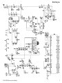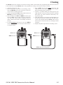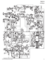
1
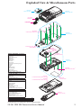
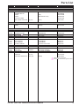
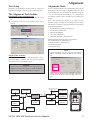
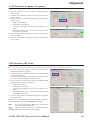
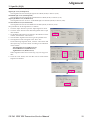
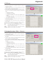
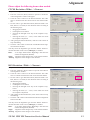
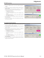
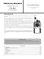
Vertex Standard LMR, Inc. VHF FM Transceiver ©2015 Vertex Standard LMR, Inc. EC128N90A VX-261 Service Manual Introduction This manual provides the technical information necessary for servicing the VX-261 VHF FM Transceiver. Servicing this equipment requires expertise in handing surface-mount chip components. Attempts by non-qualified persons to service this equipment may result in permanent damage not covered by the warranty, and may be illegal in some countries. Two PCB layout diagrams are provided for each double-sided board in this transceiver. Each side of the board is referred to by the type of the majority of components installed on that side (“Side A” or “Side B”). In most cases one side has only chip components (surface-mount devices), and the other has either a mixture of both chip and leaded components (trimmers, coils, electrolytic capacitors, ICs, etc.), or leaded components only. As described in the pages to follow, the advanced microprocessor design of the VX-261 Transceiver allows a complete alignment of this transceiver to be performed without opening the case of the radio; all adjustments can be performed from the front panel, using the “Alignment Mode” menu. While we believe the information in this manual to be correct, Vertex Standard assumes no liability for damage that may occur as a result of typographical or other errors that may be present. Your cooperation in pointing out any inconsistencies in the technical information would be appreciated. Important Note This transceiver is assembled using Pb (lead) free solder, based on the RoHS specification. Only lead-free solder (Alloy Composition: Sn-3.0Ag-0.5Cu) should be used for repairs performed on this apparatus. The solder stated above utilizes the alloy composition required for compliance with the lead-free specification, and any solder with the above alloy composition may be used. Contents Specifications................................................................................................................................................................. 2 Exploded View & Miscellaneous Parts........................................................................................................................ 3 Parts List........................................................................................................................................................................ 4 Block Diagram............................................................................................................................................................... 5 Circuit Description........................................................................................................................................................ 6 Alignment....................................................................................................................................................................... 8 Cloning......................................................................................................................................................................... 15 Main Unit Circuit Diagram........................................................................................................................................ 16 VX-261 VHF FM Transceiver Service Manual 1 Specifications General Frequency range: Channel: Power Supply Voltage: Current Consumption: Channel Spacing: PLL Steps: IP Rating: Operating Temperature Range: Charging Temperature Range: Frequency Stability: RF Input-Output: Dimension (H x W x D): Weight (Approx.): 136-174 MHz 16 Channels 7.4 V DC ± 10% 1.8 A (5 W TX) 12.5 / 25 kHz (USA Model: 12.5 kHz) 2.5 / 5 / 6.25 kHz IP55 –22 °F to +140 °F (–30 °C to +60 °C) +32 °F to +113 °F (0 °C to +45 °C) ±2.5 ppm 50 Ohm (unbalance) 2.3 x 4.3 x 1.3 inches (58.4 x 109 x 32.3 mm) (with FNB-V133LI-UNI) 2.3 x 4.3 x 1.6 inches (58.4 x 109 x 39.9 mm) (with FNB-V134LI-UNI) 9.9 oz (281 g) (with FNB-V133LI-UNI, Antenna, Belt Clip) 11.6 oz (330 g) (with FNB-V134LI-UNI, Antenna, Belt Clip) Receiver (Measured by TIA/EIA-603) Circuit Type: Sensitivity (12 dB SINAD): Adjacent Channel Selectivity: Hum and Noise: Intermodulation: Spurious Image Rejection: Conducted Spurious: Audio output: Double Conversion Super-heterodyne 0.25 µV 65 / 60 dB (W/N) 40 dB 65 dB 70 dB –57 dBm 700 mW (intemal @ 16 Ohm 5% THD) 500 mW (extemal @ 4 Ohm 5% THD) Transmitter (Measured by TIA/EIA-603) Output Power: Modulation: Maximum Deviation: Conducted Spurious Emissions: FM Hum & Noise: Audio Distortion: 5/1W 16K0F3E / 11K0F3E ±5.0 kHz / ±2.5 kHz 70 dB below carrier 40 dB <5% @ 1 kHz Specifications subject to change without notice or obligation. VX-261 VHF FM Transceiver Service Manual 2 Exploded View & Miscellaneous Parts CB6642000 MIC/SP CAP ASSY CB6987000 FRONT CASE ASSY RA1612700 KNOB (VOL) RA1612800 KNOB (FREQ) RA125020A SHIELD CASE COVER (FET) CB6992000 MAIN UNIT ASSY RA157250A (x 2 pcs) RING NUT RA1458000 RUBBER BOOTS RA037690B SHEET (6x6) FRONT CASE ASSY (Component) RA1612600 RUBBER PACKING FRONT CASE (NON KEY) NAME PLATE MODEL LABEL (VX-261) RUBBER (PTT) FLAME (PTT) RUBBER (SIDE) LATCH NAIL LATCH PLATE COIL SPRING (2.2x12x0.25) (x2 pcs) INDICATOR SPEAKER SP NET WIRE ASSY (BLK) WIRE ASSY (YEL) SHIELD SHEET SHEET (MICROTEX 8x4) PAN HEAD SCREW (M2x3BUS #2) CB6984000 CHASSIS ASSY RA0292100 SHEET (MICROTEX C010) MIC/SP CAP ASSY (Component) CAP (MIC/SP) O RING (CAP) O RING (0.8x2.2) (x2 pcs) BIND HEAD SCREW (M2.6x6B) (x2 pcs) CHASSIS ASSY (Component) AAJ67X001 Li-Ion BATTERY PACK (FNB-V133LI-UNI) or AAJ68X001 Li-Ion BATTERY PACK (FNB-V134LI-UNI) RA1614100 CAUTION LABEL CHASSIS CONNECTOR (5MAF11S-T02) RUBBER PACKING RUBBER BOOTS SHEET (6x6) SHEET (MICROTEX C010) CAUTION LABEL BIND HEAD TAPTITE-B (2x10) (x2 pcs) MAIN UNIT (Component) Printed Circuit Board with Components HOLDER RUBBER (MIC) SPONGE RUBBER (LIGHT GUIDE) SHIELD CASE COVER (FET) RING NUT (x2 pcs) PAN HEAD TAPTITE-B (M2x5) (x13 pcs) REF. VXSTD P/N DESCRIPTION U24110001 BIND HEAD TAPTITE-B 2X10 U44105001 PAN HEAD TAPTITE-B M2X5 AAH12X101 BELT CLIP (CLIP-20) QTY. 2 13 Non-designated parts are available only as part of a designated assembly. VX-261 VHF FM Transceiver Service Manual 3 Parts List REF. DESCRIPTION VALUE MFR’s DESIG VXSTD P/N FRONT CASE ASSY MIC/SP CAP ASSY CHASSIS ASSY RUBBER PACKING RUBBER BOOTS SHEET (6x6) SHEET (MICROTEX C010) CAUTION LABEL BIND HEAD TAPTITE-B (x2 pcs) (2x10) CB6987000 CB6642000 CB6984000 RA1612600 RA1458000 RA037690B RA0292100 RA1614100 U24110001 MECHANICAL PARTS KNOB KNOB RA1612700 RA1612800 CD1001 CF1001 CF1002 F 1001 MC1001 Q 1012 S 1001 S 1002 S 1003 S 1004 TH1001 VR1001 X 1001 X 1002 XF1001 MAIN UNIT ASSY CERAMIC DISC JTBM450CX24-A CERAMIC FILTER LTM450GW-A CERAMIC FILTER LTM450EW-A CHIP FUSE 3.15A, 36V FHC16 322ADTP MIC. ELEMENT PF0-1055P FET RQA0011DNS TACT SWITCH EVQPUB02K TACT SWITCH EVQPUB02K TACT SWITCH EVQPUB02K ROTARY SWITCH TP7LBJT16 RY-10487 THERMISTOR TH05 4B473FR POT. TP7LBRN1 B503 RY-10489 XTAL 11.0592MHz EXS00A-CG04670 XTAL OSC 16.8MHz HKE3448A 16.8MHZ XTAL FILTER MFT50.85P 50.85MHZ SHIELD CASE COVER (FET) RING NUT (x2 pcs) PAN HEAD TAPTITE-B (x13 pcs) (M2X5) (VOL) (FREQ) CB6992000 H7901530A H3900573A H3900574A Q0000118 M3290045 G3070392 N5090167 N5090167 N5090167 N0190199 G9090150 J60800323 H0103439 H9501511 H1102361 RA125020A RA157250A U44105001 When replace a chip fuse, use the part of the same type and value. VX-261 VHF FM Transceiver Service Manual 4 Block Diagram VX-261 VHF FM Transceiver Service Manual 5 Circuit Description 1. Receiver System 1-1. Front-end RF amplifier Incoming RF signal from the antenna is delivered to the Main Unit and passes through low-pass filter, antenna switching diode D1004 and D1005 (both 1SS390), highpass filter and removed undesired frequencies by varactor tuned band-pass filter D1007 and D1009 (both 1SV325). The filtered RF signal is amplified by Q1015 (BFS505) and then passes through another varactor tuned band-pass filter D1013 and D1014 (both 1SV325) to remove the undesired frequencies, and then applied to the 1st mixer Q1020 (3SK293). 1-2. First Mixer The RF signal is mixed with the 1st local signal between 186.85 and 224.85 MHz in the 1st mixer Q1020 (3SK293), to produce 50.85 MHz 1st IF signal. The 1st local signal is generated by the VCO, which consists of Q1029 (CPH3910), varactor diodes D1021, D1022, D1023, and D1025 (all 1SV325). The 1st local signal is supplied to the 1st mixer Q1020 (3SK293) through the buffer amplifier Q1021 and Q1026 (both 2SC5010). 1-3. IF Amplifier & Demodulator The 1st IF signal passes through monolithic crystal filters XF1001 (±7.5 kHz BW) to strip away all but the desired signal, and then supplied the buffer amplifier Q1035 (2SC5226). The amplified 1st IF signal is applied to the FM IF subsystem IC Q1040 (AA32416) which contains the 2nd mixer, 2nd local oscillator, limiter amplifier, noise amplifier, and RSSI amplifier. The signal from reference oscillator X1002 (16.8 MHz) becomes three times of frequencies in Q1040 (AA32416), it is mixed with the 1st IF signal and becomes 450 kHz. The 2nd IF signal passes through the ceramic filter CF1001 (LTM450GW) or CF1002 (LTM450EW) to strip away unwanted mixer products, and is supplied to the limiter amplifier in Q1040 (AA32416), which removes amplitude variations in the 450 kHz IF, before detection of the speech by the ceramic discriminator CD1001 (JTBM450CX24). 1-4. Audio amplifier The detected signal from Q1040 (AA32416) is supplied to the AF adder Q1045-1 (NJM12902V) through the TX/ RX switch Q1057-2 (SN74LV4066A), high-pass filter Q1045-2 (NJM12902V), and mute switch Q1057-4 (SN74LV4066A). The audio signal from Q1045-1 (NJM12902V) is supplied to the audio amplifier Q1008 (TDA2822L) through the AF volume potentiometer (VR1001). As a result, the audio signal provides up to 700 mW (@16-ohm BTL) for internal speaker or up to 500 mW (@4-ohm OTL) for external speaker. 1-5. Squelch Circuit There are 16 levels of squelch setting from “0” to “15”. The level “0” means open the squelch. The level “1” means the threshold setting level and level “14” means tight squelch. From level “2” to level “13” is established in the middle of threshold and tight. The level “15” becomes setting of carrier squelch. 1-5-1. Noise Squelch The noise squelch circuit is consisted of the band-path filter, noise amplifier Q1047 (2SC4617), and noise detector D1035 (DA221). When a carrier isn’t received, the noise ingredient which goes out of the demodulator section of Q1040 (AA32416) is amplified by noise amplifier Q1047 (2SC4617) through the band-path filter, and then is detected to DC voltage by D1035 (DA221). The DC voltage is inputted to pin 54 (A/D port) of the CPU Q1028 (R5F100LHDFB). When a carrier is received, the DC voltage becomes low because the noise is compressed. When the detected voltage to CPU is “High”, the CPU stops the AF output of Q1013 (DTC144EE) by making to “low” of the pin 39 of CPU. When the detection voltage to CPU is “low”, the CPU allows the AF output of Q1013 (DTC144EE) by making to “High” of the pin 39 of CPU. 1-5-2. Carrier Squelch The detected RSSI voltage from pin 12 of Q1040 (AA32416) supplied to pin 53 (A/D port) of Q1028 (R5F100LHDFB). It is controls the AF output. The RSSI output voltage changes according to the signal strength of carrier. The stronger signal makes the RSSI voltage to be higher voltage. The process of the AF signal control is same as Noise Squelch. The shipping data is adjusted 3 dBµ (EMF) higher than squelch tight sensitivity. VX-261 VHF FM Transceiver Service Manual 6 Circuit Description 2. Transmitter System 3. PLL Frequency Synthesizer The speech signal from internal microphone MC1001 or external microphone J1003 is amplified by Q1044-2 (NJM12902V). While the radio is receiving, the RX VCO Q1029 (CPH3910) generates a programmed frequency between 186.85 and 224.85 MHz as 1st local signal. 2-1. MIC Amplifier The amplified speech signal from Q1044-2 (NJM12902V) is supplied to pin 14 of Electric Volume IC Q1018 (AK2330) which adjusts the microphone gain through the TX/RX switch Q1057-2 (SN74LV4066A), high-pass filter Q1045-2 (NJM12902V), and other TX/RX switch Q1057-3 (SN74LV4066A). The adjusted speech signal is output from pin 15 of Q1018 (AK2330), and then passed through the limiter amplifier Q1044-1 (NJM12902V), low-pass filter Q1044-2/-3 (NJM12902V), and AF adder Q1052-3 (NJM12902V). The processed speech signal from Q1052-3 (NJM12902V) is supplied to pin 22 of Electric Volume IC Q1018 (AK2330) which adjusts the maximum deviation. The adjusted speech signal is amplified by Q10522 (NJM12904R), and then is made FM modulation to transmit carrier by the modulator D1019 (BB208) of VCO Q1037 (2SC4227). 2-2. Drive and Final Amplifier Stages The modulated signal from the VCO Q1037 (2SC4227) is buffered by Q1026 (2SC5010). Then the signal is buffered by Q1021 (2SC5010) and Q1019 (2SK3077) for the driver amplifier Q1016 (RQA0004PXDQS). The low-level transmit signal is then applied to Q1012 (RQA0011DNS) for final amplification up to 5 watts output power. The transmit signal then passes through the antenna switch D1003 (RN142S) and is low-pass filtered to suppress away harmonic spurious radiation before delivery to the antenna. 2-3. Automatic Transmit Power Control The current detector Q1053-1 (NJM12904R) detects the current of the driver amplifier Q1016 (RQA0004PXDQS) and final amplifier Q1012 (RQA0011DNS), and converts the current difference to the voltage difference. The output from the current detector Q1053-1 (NJM12904R) is compared with the reference voltage by Q1053-2 (NJM12904R). The output from Q1053-2 (NJM12904R) controls the gate bias of the driver amplifier Q1016 (RQA0004PXDQS) and final amplifiers Q1012 (RQA0011DNS). The reference voltage changes into two levels (Transmit Power “High” and “Low”) controlled by the Electric Volume IC Q1018 (AK2330). 3-1. VCO (Voltage Controlled Oscillator) While the radio is transmitting, the TX VCO Q1037 (2SC4227) generates a frequency between 136 and 174 MHz. The output from VCO is amplified by buffer amplifier Q1026 and Q1021 (both 2SC5010). The buffered VCO is supplied to the 1st mixer Q1020 (3SK293) in case of the reception. In the transmission, the buffered VCO is supplied to other buffer amplifier Q1019 (2SK3077), and then amplified more by Q1016 (RQA0004PXDQS) and it is put into the final amplifier Q1012 (RQA0011DNS). A portion of the buffered VCO is fed back to the PLL IC Q1046 (AK1541) to control the VCV voltage. 3-2. Varactor Control Voltage The tuning voltage (VCV) of VCO is established the lock range of VCO by controlling the cathode of varactor diodes D1021, D1022, D1023, and D1025 (all 1SV325) for receiving, and D1027 and D1028 (both 1SV325) for transmitting. 3-3. PLL The PLL IC Q1046 (AK1541) is consists of reference divider, main divider, phase detector, charge pumps, and pulse swallow operation. The reference frequency from TCXO X1002 (16.8 MHz) is inputted to pin 10 of PLL IC Q1046 (AK1541) and is divided by reference divider. On the other hand, the feedback signal of the VCO inputted to 17 pin of PLL IC Q1046 (AK1541), and is divided with the dividing ratio which becomes same frequency as the output of reference divider. These two signals are compared by phase detector, and then phase difference pulse is generated. The phase difference pulse is becomes a DC voltage through the charge pumps and LPF, and it controls the VCO. The PLL serial data from CPU Q1028 (R5F100LHDFB) is sent with three lines of SDO (pin 5), SCK (pin 6) and PSTB (pin 4). The lock condition of PLL is output from the UL (pin 7) terminal of the PLL IC Q1046 (AK1541). The UL terminal becomes “High” at the lock condition, and becomes “Low” at the unlock condition. The CPU Q1028 (R5F100LHDFB) is always watching over the UL condition, and when it becomes “Low” unlocked condition, the CPU prohibits transmitting and receiving. VX-261 VHF FM Transceiver Service Manual 7 Alignment Introduction The VX-261 is carefully aligned at the factory for the specified performance across the frequency range specified for each version. Realignment should therefore not be necessary except in the event of a component failure, or altering version type. All component replacement and service should be performed only by an authorized Vertex Standard representative, or the warranty policy may be void. The following procedures cover the sometimes critical and tedious adjustments that are not normally required once the transceiver has left the factory. However, if damage occurs and some parts subsequently are replaced, realignment may be required. If a sudden problem occurs during normal operation, it is likely due to component failure; realignment should not be done until after the faulty component has been replaced. We recommend that servicing be performed only by authorized Vertex Standard service technicians who are experienced with the circuitry and fully equipped for repair and alignment. Therefore, if a fault is suspected, contact the dealer from whom the transceiver was purchased for instructions regarding repair. Authorized Vertex Standard service technicians realign all circuits and make complete performance checks to ensure compliance with factory specifications after replacing any faulty components. Those who do undertake any of the following alignments are cautioned to proceed at their own risk. Problems caused by unauthorized attempts at realignment are not covered by the warranty policy. Also, Vertex Standard reserves the right to change circuits and alignment procedures in the interest of improved performance, without notifying owners. Under no circumstances should any alignment be attempted unless the normal function and operation of the transceiver are clearly understood, the cause of the malfunction has been clearly pinpointed and any faulty components replaced, and realignment determined to be absolutely necessary. The following test equipment (and thorough familiarity with its correct use) is necessary for complete realignment. Correction of problems caused by misalignment resulting from use of improper test equipment is not covered under the warranty policy. While most steps do not require all of the equipment listed, the interactions of some adjustments may require that more complex adjustments be performed afterwards. Do not attempt to perform only a single step unless it is clearly isolated electrically from all other steps. Have all test equipment ready before beginning, and follow all of the steps in a section in the order presented. Required Test Equipment RF Signal Generator with calibrated output level at 600 MHz Oscilloscope Deviation Meter (linear detector) In-line Wattmeter with 5 % accuracy at 200 MHz 50 Ohm RF Dummy Load with power rating 10 W at 600 MHz Regulated DC Power Supply (standard 7.5 V DC, 3 A) Frequency Counter with 0.2 ppm accuracy at 200 MHz Audio Signal Generator AC Voltmeter DC Voltmeter VHF Sampling Coupler IBM® PC/compatible Computer with Microsoft® Windows® 2000, XP, Vista or Windows7 Vertex Standard CE150 PC Programming Software Vertex Standard FIF-12 USB Programming Interface and CT-104A, CT-106, or CT-171 PC Programming Cable. Vertex Standard FRB-6 Tuning Interface Box and CT160 Connection Cable. Vertex Standard CN-3 (P/N: A08760001) Antenna Connector Alignment Preparation & Precautions A 50-Ohm RF Dummy Load and in-line wattmeter must be connected to the main antenna jack in all procedures that call for transmission, except where specified otherwise. Correct alignment is not possible with an antenna. Because of the BTL (Bridged Trans Less) Amplifier circuit used in the VX-261, do not connect earth side of the speaker leads to chassis “ground”. After completing one step, read the following step to determine whether the same test equipment will be required. If not, remove the test equipment (except dummy load and wattmeter, if connected) before proceeding. Correct alignment requires that the ambient temperature be the same as that of the transceiver and test equipment, and that this temperature be held constant between 68 and 86 °F (20 ~ 30 °C). When the transceiver is brought into the shop from hot or cold air, it should be allowed time to come to room temperature before alignment. Whenever possible, alignments should be made with oscillator shields and circuit boards firmly affixed in place. Also, the test equipment must be thoroughly warmed up before beginning. Note: Signal levels in dB referred to in the alignment procedure are based on 0 dBµ EMF = 1 µV. VX-261 VHF FM Transceiver Service Manual 8 Alignment Test Setup Setup the test equipment as shown below for transceiver alignment, then apply 7.5 V DC power to the transceiver. The Alignment Tool Outline Installation of the alignment tool Install the CE150 (PC Programming Software) to your PC. “Alignment“ function in the “Radio“ menu tab of CE150. Alignment Mode In the “Alignment Mode”, the aligned data written in the radio will be able to re-align its alignment data. The value of each parameter can be changed to desired position by “”/“” arrow key for data up/down, “”/“” arrow key for channel up/down, direct number input, and drag the mouse. Note: when all items are aligned, it is strongly recommended to align according to following order. The detail information is written in the help document of CE150 PC Programming Software. 1. 2. 3. 4. 5. ê PLL Reference Frequency (Frequency) RX Sensitivity (RX Tune) Squelch (SQL/RSSI) TX Power <High/Low> Maximum Deviation <Wide/Narrow> Please adjust the following items when needed. ¦ CTCSS Deviation <Wide/Narrow> ¦ DCS Deviation <Wide/Narrow> ¦ DTMF Alignment ¦ Sequential Tone Unit During alignment, you may select the value among dBµV, µV (EMF or PD), or dBm by the “UNIT” box. Action of the switches When the transceiver is in the “Alignment mode,“ the action of the SIDE-1, SIDE-2, and PTT keys are ignored. All of the action is controlled by the PC. Caution Please never turn off the power supply during alignment. If the power supply is turned off during alignment, the alignment data will be corrupted. When perform the RX Tune and SQL alignment, the RF level shows this unit according to this setting. 50-ohm Dummy Load SP/LOAD Switch: LOAD LOAD Switch: 16 RF Signal Generator SINAD Meter CT-160 SP OUT B Inline Wattmeter Deviation Meter Frequency Counter Sampling Coupler ANT MIC/SP AF Signal Transceiver FRB-6 D-Sub 15-pin MIC IN Generator Connector Battery Terminal CLONE Port CT-104A, CT-106, or CT-171 Power Supply 7.5 VDC FIF-12 Computer (CE150) Oscilloscope VX-261 VHF FM Transceiver Service Manual 9 Alignment 1.PLL Reference Frequency (Frequency) This parameter align the reference frequency for PLL. 1. Press the “Frequency” button to open the “Frequency Alignment” window. 2. Click the “PTT” button to transmit the radio on the center frequency channel. 3. Set the value to get the desired frequency according to the following ways: Dragging the slide bar Clicking the arrow buttons Pressing the left/right arrow key of the computer’s keyboard Entering the value (“000” - “255”) in the “Data” box from the computer’s keyboard 4. After getting the desired frequency, click the “PTT” button to stop transmitting. 5. Click the “OK” button to finish the frequency alignment and save the data. ê 2.RX Sensitivity (RX Tune) This parameter align the RX BPF (Band Pass Filter) for Receive (RX) sensitivity. The PLL Reference Frequency (Frequency) alignment must be done before this alignment is performed. 1. Press the “RX Tune” button to open the “RX Sensitivity Alignment” window will appear. 2. Click the slide bar of the desired channel. The radio switches to the selected channel. 3. Set the RF Signal Generator according to the indication at the top of the screen (Setting Your SG as followings). 4. Set the value to get the best RX sensitivity (Highest RSSI value) according to the following ways: Dragging the slide bar Clicking the arrow buttons Pressing the left/right arrow key of the computer’s keyboard Entering the value (“000” - “255”) in the “Data” box from the computer’s keyboard 5. Click the “OK” button to finish the RX Sensitivity alignment and save the data. ê You may select the alignment type from the “Radio” button located at the button of the screen (ADJ Type), as needed. Basic: “Low Edge / Band Center/ High Edge” and select the channel for alignment (Default). Single: Alignment value changes only on the selected channel. All Freq: Alignment value changes on all channels. VX-261 VHF FM Transceiver Service Manual 10 Alignment 3.Squelch (SQL) This parameter align the SQL (Squelch) Sensitivity. There are several alignments as follows in the Squelch Sensitivity. Tight SQL Level (TI NSQ W/N) The Alignment for the Noise SQL Tight level at Wide (5k/4k) or Narrow (2.5k). Threshold SQL Level (TH NSQ W/N) The Alignment for the Noise SQL Threshold level at Wide (5k/4k) or Narrow (2.5k). Tight SQL RSSI Level (TI RSSI W/N) The Alignment for the “level 14” of the RSSI SQL level at Wide (5k/4k) or Narrow (2.5k). TX Save RSSI Level (TX SAVE W/N) The Alignment for the TX Save RSSI level at Wide (5k/4k) or Narrow (2.5k). The procedure for all the alignments is as follows. 1. Click the “SQL” button to open the “SQL Alignment” menu. 2. Click the “Start” button on the desired alignment item to open other window. 3. Set the RF Signal Generator according to the indication of the window, then click the “OK” button. 4. The automatic alignment will start to get the optimum level. 5. The alignment result will appear in the “New” box. On the following alignment items, click the “OK” button and then repeat step 2-5 several times according to the indication of the window. Threshold SQL Level (Wide/Narrow) Normal RSSI Level (Wide/Narrow) Tight RSSI Level (Wide/Narrow) Other alignment items has not extra step; only one step procedure. 6. Click the “OK” button, then the data will be saved and the alignment is finished. ê ê ê VX-261 VHF FM Transceiver Service Manual 11 Alignment 4.TX Power This parameter align the Transmit Output “High” or “Low” Power for the selected channel. 1. Press the “TX Power (H / L)” button to open the “TX Power Alignment” window. 3. Click the “PTT” button on the desired channel. The radio starts to transmit on the selected channel. 4. Set the value to get desired output power (Normally: High: 5 W, Low: 1 W) on the Power Meter according to the following ways: Dragging the slide bar Clicking the arrow buttons Pressing the left/right arrow key of the computer’s keyboard Entering the value (“000” - “255”) in the “Data” box from the computer’s keyboard 5. After getting the desired output power, click the “PTT” button to stop transmitting. 6. Click the “OK” button to finish the TX Power alignment and save the data. ê You may select the alignment type from the “Radio” button located at the button of the screen (ADJ Type), as needed. Basic: “Low Edge / Band Center/ High Edge” and select the channel for alignment (Default). Single: Alignment value changes only on the selected channel. All Freq: Alignment value changes on all channels. 5.Maximum Deviation <Wide> / <Narrow> This parameter align the Maximum Deviation (Wide/Narrow). 1. Press the “Max Dev (W /N)” button to open the “Max Deviation Alignment” window. 2. Set the Audio Signal Generator to 100 mV with a 1 kHz tone, Sine Wave. 3. Click the “PTT” button on the desired channel. The radio starts to transmit on the selected channel. 4. Set the value to get desired deviation (Wide: 4.2 kHz, Narrow: 2.1 kHz) on the deviation meter according to the following ways: Dragging the slide bar Clicking the arrow buttons Pressing the left/right arrow key of the computer’s keyboard Entering the value (“000” - “255”) in the “Data” box from the computer’s keyboard 5. After getting the desired deviation, click the “PTT” button to stop transmitting. 6. Click the “OK” button to finish the Max Deviation alignment and save the data. ê You may select the alignment type from the “Radio” button located at the button of the screen (ADJ Type), as needed. Basic: “Low Edge / Band Center/ High Edge” and select the channel for alignment (Default). Single: Alignment value changes only on the selected channel. All Freq: Alignment value changes on all channels. VX-261 VHF FM Transceiver Service Manual 12 Alignment Please adjust the following items when needed. CTCSS Deviation <Wide> / <Narrow> This parameter align the CTCSS Deviation of the selected channel. 1. Press the “CTC Dev (W/N)” button to open the “CTCSS Deviation Alignment” window will appear. 2. Click the “PTT” button on the desired channel. The radio starts to transmit with the CTCSS tone on the selected channel. 3. Set the value to get desired deviation (Nominal: Wide: 0.55 kHz, Narrow: 0.35 kHz) on the deviation meter according to the following ways: Dragging the slide bar Clicking the arrow buttons Pressing the left/right arrow key of the computer’s keyboard Entering the value (“0” - “255”) in the “Data” box from the computer’s keyboard 4. After getting the desired deviation, click the “PTT” button to stop transmitting. 5. Click the “OK” button to finish the CTCSS Deviation alignment and save the data. ê You may select the alignment type from the “Radio” button located at the button of the screen (ADJ Type), as needed. Basic: “Low Edge / Band Center/ High Edge” and select the channel for alignment (Default). Single: Alignment value changes only on the selected channel. All Freq: Alignment value changes on all channels. DCS Deviation <Wide> / <Narrow> This parameter is to align the DCS Deviation of the selected channel. 1. Press the “DCS Dev (W/N)” button to open the “DCS Deviation Alignment” window. 2. Click the “PTT” button on the desired channel. The radio starts to transmit with the DCS code on the selected channel. 3. Set the value to get desired deviation (Nominal: Wide: 0.55 kHz, Narrow: 0.35 kHz) on the deviation meter according to the following ways: Dragging the slide bar Clicking the arrow buttons Pressing the left/right arrow key of the computer’s keyboard Entering the value (“0” - “255”) in the “Data” box from the computer’s keyboard 4. After getting the desired deviation, click “PTT” button to stop transmitting. 5. Click the “OK” button to finish the DCS Deviation alignment and save the data. ê You may select the alignment type from the “Radio” button located at the button of the screen (ADJ Type), as needed. Basic: “Low Edge / Band Center/ High Edge” and select the channel for alignment (Default). Single: Alignment value changes only on the selected channel. All Freq: Alignment value changes on all channels. VX-261 VHF FM Transceiver Service Manual 13 Alignment DTMF Deviation This parameter align the DTMF Deviation. 1. Press the “DTMF” button to open the “DTMF Alignment” window. 2. Click the “PTT” button to transmit the radio on the center frequency channel. 3. Set the value to get desired deviation (Nominal: 3.0 kHz) on the deviation meter according to the following ways: Dragging the slide bar Clicking the arrow buttons Pressing the left/right arrow key of the computer’s keyboard Entering the value (“0” - “255”) in the “Data” box from the computer’s keyboard 4. After getting the desired deviation, click the “PTT” button to stop transmitting. 5. Click the “OK” button to finish the DTMF Deviation alignment and save the data. ê Sequential Tone Deviation This parameter align the Sequential Tone Deviation for the 2-Tone and 5-Tone Encoder. 1. Press the “Seq Tone” button to open the “Sequential Tone Deviation Alignment” window will appear. 2. Click the “PTT” button to transmit the radio on the center frequency channel. 3. Set the value to get desired deviation (Nominal: 3.0 kHz) on the deviation meter according to the following ways: Dragging the slide bar Clicking the arrow buttons Pressing the left/right arrow key of the computer’s keyboard Entering the value (“0” - “255”) in the “Data” box from the computer’s keyboard 4. After getting the desired deviation, click the “PTT” button to stop transmitting. 5. Click the “OK” button to finish the Sequential Tone Deviation alignment and save the data. VX-261 VHF FM Transceiver Service Manual ê 14 Cloning The VX-261 transceiver includes a convenient “Cloning” feature, which allows the programming data from one transceiver to be transferred to another VX-261. Here is the procedure for Cloning one transceiver’s data to another. 1. Turn both transceivers “off”. 2. Remove the plastic cap and its two mounting screws from the MIC/SP jack on the right side of the transceiver. Do this for both transceivers. 3. Connect the optional CT-27 cloning cable between the MIC/SP jacks of the two transceivers. 4. Press and hold in the PTT and SIDE-1 switches (just below the PTT switch) while turning the transceiver “on” (the order of the switch-on operation does not matter). When Clone mode is successfully activated in this step. 5. On the Destination transceiver, press the SIDE-1 switch. The LED indicator on the top of the transceiver will glow Green. 6. Press the PTT switch on the Source transceiver. The LED indicator on the top of the transceiver will glow Red, and the data will be transferred. 7. If there is a problem during the cloning process, the LED indicator on the top of the transceiver will blink Red; check your cable connections and battery voltage, and try again. 8. If the data transfer is successful, the LED indicator on the top of the transceiver will turn off. Turn both transceivers “off” and disconnect the CT-27 cable. You can then turn the transceivers back on, and begin normal operation. 9. Replace the plastic cap and its two mounting screws. PTT Switch PTT Switch SIDE-1 Switch SIDE-1 Switch CT-27 Optional Cloning Cable VX-261 VHF FM Transceiver Service Manual 15 Main Unit Circuit Diagram VX-261 VHF FM Transceiver Service Manual 16 No portion of this manual may be reproduced without the permission of Vertex Standard LMR, Inc. Vertex Standard is a trademark of Vertex Standard LMR, Inc. All other trademarks are the property of their respective owners. ©2015 Vertex Standard LMR, Inc. All rights reserved. VX-261 VHF FM Transceiver Service Manual 16