1
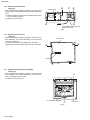
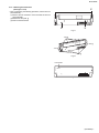
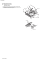
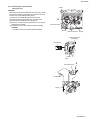
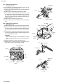
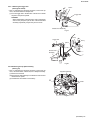
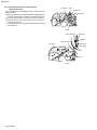
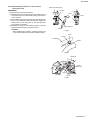
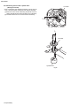
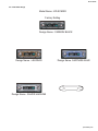
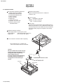
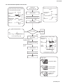
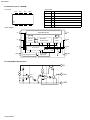
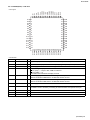
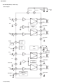
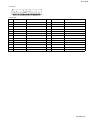
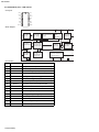
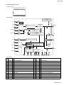
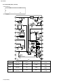
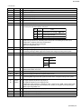
KD-SC900R
SERVICE MANUAL
CD RECEIVER
04
2003
49829
KD-SC900R
Area Suffix
E ------------- Continental Europe
EX ---------------- Central Europe
TABLE OF CONTENTS
1
2
3
4
Important Safety Precautions . . . . . . . . . . . . . . . . . . . . . . . . . . . . . . . . . . . . . . . . . . . . . . . . . . . . . . . . . . . 1-2
Disassembly method . . . . . . . . . . . . . . . . . . . . . . . . . . . . . . . . . . . . . . . . . . . . . . . . . . . . . . . . . . . . . . . . . . 1-4
Adjustment. . . . . . . . . . . . . . . . . . . . . . . . . . . . . . . . . . . . . . . . . . . . . . . . . . . . . . . . . . . . . . . . . . . . . . . . . . 1-24
Description of major ICs . . . . . . . . . . . . . . . . . . . . . . . . . . . . . . . . . . . . . . . . . . . . . . . . . . . . . . . . . . . . . . . 1-28
COPYRIGHT © 2003 VICTOR COMPANY OF JAPAN, LTD.
No.49829
2003/04
KD-SC900R
SECTION 1
Important Safety Precautions
1.1 Safety Precautions
!
Burrs formed during molding may be left over on some parts of the chassis. Therefore,
pay attention to such burrs in the case of preforming repair of this system.
!
Please use enough caution not to see the beam directly or touch it in case of an
adjustment or operation check.
1-2 (No.49829)
KD-SC900R
1.2 Preventing static electricity
Electrostatic discharge (ESD), which occurs when static electricity stored in the body, fabric, etc. is discharged,
can destroy the laser diode in the traverse unit (optical pickup). Take care to prevent this when performing repairs.
1.2.1 Grounding to prevent damage by static electricity
Static electricity in the work area can destroy the optical pickup (laser diode) in devices such as DVD players.
Be careful to use proper grounding in the area where repairs are being performed.
(1) Ground the workbench
Ground the workbench by laying conductive material (such as a conductive sheet) or an iron plate over it before placing the
traverse unit (optical pickup) on it.
(2) Ground yourself
Use an anti-static wrist strap to release any static electricity built up in your body.
(caption)
Anti-static wrist strap
1M
Conductive material
(conductive sheet) or iron plate
(3) Handling the optical pickup
• In order to maintain quality during transport and before installation, both sides of the laser diode on the replacement optical
pickup are shorted. After replacement, return the shorted parts to their original condition.
(Refer to the text.)
• Do not use a tester to check the condition of the laser diode in the optical pickup. The tester's internal power source can easily
destroy the laser diode.
1.3 Handling the traverse unit (optical pickup)
(1) Do not subject the traverse unit (optical pickup) to strong shocks, as it is a sensitive, complex unit.
(2) Cut off the shorted part of the flexible cable using nippers, etc. after replacing the optical pickup. For specific details, refer to the
replacement procedure in the text. Remove the anti-static pin when replacing the traverse unit. Be careful not to take too long
a time when attaching it to the connector.
(3) Handle the flexible cable carefully as it may break when subjected to strong force.
(4) I t is not possible to adjust the semi-fixed resistor that adjusts the laser power. Do not turn it.
1.4 Attention when traverse unit is decomposed
*Please refer to "Disassembly method" in the text for the CD pickup unit.
• Apply solder to the short land before the flexible wire is disconnected from the connector on the CD pickup unit.
(If the flexible wire is disconnected without applying solder, the CDpickup may be destroyed by static electricity.)
• In the assembly, be sure to remove solder from the short land after connecting the flexible wire.
Short-circuit point
(Soldering)
Flexible wire
Pickup
Short-circuit point
Pickup
(No.49829)1-3
KD-SC900R
SECTION 2
Disassembly method
2.1 Main body
2.1.1 Removing the front panel assembly
(See Fig.1)
(1) Push the detach button in the lower left part of the front
panel assembly and remove the front panel assembly in
the direction of the arrow.
Front panel assembly
Detach button
Fig.1
2.1.2 Removing the front chassis assembly
(See Figs.2 to 4)
• Prior to performing the following procedure, remove the front
panel assembly.
(1) Remove the screw A on the both sides of the main body.
(2) Remove the two screws B on the front side of the main
body.
(3) Release the two joints a and two joints b on both sides of
the main body using a screwdriver, and remove the front
chassis assembly forward.
(4) Release the two joints c on the bottom side of the main
body and remove the front chassis assembly in the direction of the arrow.(see Fig.3)
Joint a
Joint b
A
A
Joint a
Joint b
Front chassis assembly
Fig.2
B
Fig.3
Front chassis assembly
Joint c
Joint c
Fig.4
1-4 (No.49829)
KD-SC900R
2.1.3 Removing the heat sink
(See Fig.5)
(1) Remove the two screws C and one screws D on the left
side of the main body.
C
D
Heat sink
Fig.5
2.1.4 Removing the bottom cover
(See Figs.6 and 7)
• Prior to performing the following procedure, remove the front
panel assembly, front chassis assembly and heat sink.
(1) Turn over the body and release the two joints d, two joints
e and joint f .
Joint d
Bottom cover
CAUTION:
Do not damage the main board when releasing the joint d using a screwdriver. (See Figs.6 and 7)
Joint f
Joint e
Fig.6
Joint e
Bottom cover
Joint f
Joint d
Fig.7
(No.49829)1-5
KD-SC900R
2.1.5 Removing the rear bracket
(See Fig.8)
• Prior to performing the following procedure, remove the front
panel assembly, front chassis assembly, heat sink and bottom
cover.
(1) Remove the three screws E, one screws F and two screws
G on the back of the body.
(2) Remove the rear bracket.
Rear bracket
G
F
E
G
E
Insert Subwoofer and steering
cables into the slots.
Fig.8
2.1.6 Removing the main board
(See Fig.9)
• Prior to performing the following procedure, remove the front
panel assembly, front chassis assembly, heat sink, bottom
cover and rear bracket.
(1) Remove the two screws H attaching the main board.
(2) Disconnect connector CN501 and remove the main board.
Main board
H
H
CN501
Fig.9
2.1.7 Removing the CD mechanism assembly
(See Fig.10)
• Prior to performing the following procedure, remove the front
panel assembly, front chassis assembly, heat sink, bottom
cover, rear bracket and main board.
(1) Remove the three screws J .
J
CD mechanism assembly
J
Fig.10
1-6 (No.49829)
Top chassis
KD-SC900R
2.1.8 Removing the front board
(See Figs.11 to 13)
• Prior to performing the following procedure, remove the front
panel assembly.
(1) Remove the four screws K on the back side of the front
panel assembly.
(2) Release the ten joints g.
(3) Take out the front board.
K
K
K
Fig.11
Joint g
Joint g
Joint g
Joint g
Fig.12
Front board
Fig.13
(No.49829)1-7
KD-SC900R
2.2 CD Mechanism Assembly
2.2.1 Removing the top cover
(See Figs.1 and 2)
(1) Remove the two screws A on the both side of the body.
(2) Lift the front side of the top cover and move the top cover
backward to release the two joints a.
A
Top cover
Joints a
A
A
Fig.1
Joints a
Top cover
Fig.2
1-8 (No.49829)
KD-SC900R
2.2.2 Removing the connector board
(See Figs.3 to 5)
CAUTION:
Before disconnecting the flexible wire from the pickup, solder
the short-circuit point on the pickup. No observance of this instruction may cause damage of the pickup.
(1) Remove the screw B fixing the connector board.
(2) Solder the short-circuit point on the connector board.
(3) Disconnect the flexible wire from the pickup.
(4) Move the connector board in the direction of the arrow to
release the two joints b.
(5) Unsolder the wire on the connector board if necessary.
Wires
B
Connector board
CAUTION:
Unsolder the short-circuit point after reassembling.
Joints b Short-circuit point
Fig.3
Pickup
Short-circuit point
(Soldering)
Flexible wire
Pickup
Fig.4
Connector board
B
Flexible wire
Frame
Fig.5
(No.49829)1-9
KD-SC900R
2.2.3 Removing the DET switch
(See Figs.6 and 7)
(1) Extend the two tabs c of the feed sw. holder and pull out
the switch.
(2) Unsolder the DET switch wire if necessary.
DET switch
Connector
board
Pickup
Fig.6
DET switch
Tab c
DET switch wire
Tab c
Feed sw. holder
Fig.7
1-10 (No.49829)
KD-SC900R
2.2.4 Removing the chassis unit
(See Figs.8 and 9)
• Prior to performing the following procedure, remove the top
cover and connector board.
(1) Remove the two suspension springs (L) and (R) attaching
the chassis unit to the frame.
Chassis unit
Suspension spring (L)
Suspension spring (R)
Frame
CAUTION:
• The shape of the suspension spring (L) and (R) are different. Handle them with care.
• When reassembling, make sure that the three shafts
on the underside of the chassis unit are inserted to the
dampers certainly.
Suspension spring (R)
Suspension spring (L)
Fig.8
Chassis unit
Shaft
Shafts
Damper
Damper
Frame
Damper
Fig.9
(No.49829)1-11
KD-SC900R
2.2.5 Removing the clamper assembly
(See Figs.10 and 11)
• Prior to performing the following procedure, remove the top
cover.
(1) Remove the clamper arm spring.
(2) Move the clamper assembly in the direction of the arrow to
release the two joints d.
Clamper arm
spring
Joint d
Clamper assembly
Fig.10
Chassis rivet
assembly
Joint d
Clamper arm spring
Joint d
Clamper
assembly
Joint d
Chassis rivet assembly
Fig.11
1-12 (No.49829)
KD-SC900R
2.2.6 Removing the loading / feed motor assembly
(See Figs.12 and 13)
• Prior to performing the following procedure, remove the top
cover, connector board and chassis unit.
(1) Remove the screw C and move the loading / feed motor
assembly in the direction of the arrow to remove it from the
chassis rivet assembly.
(2) Disconnect the wire from the loading / feed motor assembly
if necessary.
CAUTION:
When reassembling, connect the wire from the loading /
feed motor assembly to the flame as shown in Fig.12.
Loading / feed motor assembly
Fig.12
Loading / feed motor assembly
C
Fig.13
(No.49829)1-13
KD-SC900R
2.2.7 Removing the pickup unit
(See Figs.14 to 18)
• Prior to performing the following procedure, remove the top
cover, connector board and chassis unit.
(1) Remove the screw D and pull out the pu. shaft holder from
the pu. shaft.
(2) Remove the screw E attaching the feed sw. holder.
(3) Move the part e of the pickup unit upward with the pu. shaft
and the feed sw. holder, then release the joint f of the feed
sw. holder in the direction of the arrow. The joint g of the
pickup unit and the feed rack is released, and the feed sw.
holder comes off.
(4) Remove the pu. shaft from the pickup unit.
(5) Remove the screw F attaching the feed rack to the pickup
unit.
2.2.8 Reattaching the pickup unit
(See Figs.14 to 17)
(1) Reattach the feed rack to the pickup unit using the screw F.
(2) Reattach the feed sw. holder to the feed rack while setting
the joint g to the slot of the feed rack and setting the part f
of the feed rack to the switch of the feed sw. holder correctly.
(3) As the feed sw. holder is temporarily attached to the pickup
unit, set to the gear of the joint g and to the bending part of
the chassis (joint h) at a time.
CAUTION:
Make sure that the part i on the underside of the feed
rack is certainly inserted to the slot j of the change lock
lever.
(4) Reattach the feed sw. holder using the screw E.
(5) Reattach the pu. shaft to the pickup unit. Reattach the pu.
shaft holder to the pu. shaft using the screw D.
Pickup unit
Part e
Feed rack
Feed sw. holder
Fig.15
Pu. shaft
Part i Pickup unit
D
E
Slot j
Joint g
Joint f
Joint h
Pu. shaft
holder
Feed sw.
holder
Fig.16
F
Feed rack
Feed sw. holder
Pickup unit
Joint f
E
Fig.17
Pu. shaft
Joint g
D
Pickup unit
Joint g
Pickup unit Part e
Pu. shaft holder
Fig.14
Joint f
Feed rack
1-14 (No.49829)
Feed sw. holder
Fig.18
KD-SC900R
2.2.9 Removing the trigger arm
(See Figs.19 and 20)
• Prior to performing the following procedure, remove the top
cover, connector board and clamper unit.
(1) Turn the trigger arm in the direction of the arrow to release
the joint k and pull out upward.
Joint k
Trigger arm
CAUTION:
When reassembling, insert the part m and n of the trigger
arm into the part p and q at the slot of the chassis rivet
assembly respectively and join the joint k at a time.
Chassis rivet assembly
Fig.19
Part p
Trigger arm
Part q
Part m
Part n
Chassis rivet
assembly
Fig.20
2.2.10 Removing the top plate assembly
(See Fig.21)
• Prior to performing the following procedure, remove the top
cover, connector board, chassis unit, and clamper assembly.
(1) Remove the screw H.
(2) Move the top plate assembly in the direction of the arrow to
release the two joints r.
(3) Unsolder the wire marked s if necessary.
Top plate assembly
H
Joints r
s
Fig.21
(No.49829)1-15
KD-SC900R
2.2.11 Removing the mode sw. / select lock arm
(See Figs.22 and 23)
• Prior to performing the following procedure, remove the top
plate assembly.
(1) Bring up the mode sw. to release from the link plate (joint t)
and turn in the direction of the arrow to release the joint u.
(2) Unsolder the wire of the mode sw. marked s if necessary.
(3) Turn the select lock arm in the direction of the arrow to release the two joints v.
(4) The select lock arm spring comes off the select lock arm at
the same time.
Link plate
Joint t
Mode sw.
Select lock arm
Joint u
s
Fig.22
Select lock arm
Top plate
Hook w
Select lock arm
Top plate
Select lock
arm spring
Joints v
Link plate
Fig.23
1-16 (No.49829)
KD-SC900R
2.2.12 Reassembling the mode sw. / select lock arm
(See Figs.24 to 26)
Select lock arm spring
Hook w
REFERENCE:
Reverse the above removing procedure.
(1) Reattach the select lock arm spring to the top plate and set
the shorter end of the select lock arm spring to the hook w
on the top plate.
(2) Set the other longer end of the select lock arm spring to the
boss x on the underside of the select lock arm, and join the
select lock arm to the slots (joint v). Turn the select lock
arm as shown in the figure.
(3) Reattach the mode sw. while setting the part t to the first
peak of the link plate gear, and join the joint u.
Joint v
Joint v
Select lock arm
Boss x
CAUTION:
When reattaching the mode sw., check if the points y and
z are correctly fitted and if each part operates properly.
Fig.24
Joint t
Point y
Link plate
Point z
Fig.25
Mode sw.
Select
lock arm
Joint t
Link plate
Joint u
Fig.26
(No.49829)1-17
KD-SC900R
2.2.13 Removing the select arm R / link plate
(See Figs.27 and 28)
• Prior to performing the following procedure, remove the top
plate assembly.
(1) Bring up the select arm R to release from the link plate
(joint a') and turn as shown in the figure to release the two
joints b' and joint c'.
(2) Move the link plate in the direction of the arrow to release
the joint d'. Remove the link plate spring at the same time.
Select arm R
Link plate
Joint c'
Joint b'
Joint r
Joint b'
REFERENCE:
Before removing the link plate, remove the mode sw..
Joint a'
Fig.27
Link plate spring
Top plate
Joint d'
Link plate
Fig.28
2.2.14 Reattaching the Select arm R / link plate
(See Figs.29 and 30)
REFERENCE:
Reverse the above removing procedure.
(1) Reattach the link plate spring.
(2) Reattach the link plate to the link plate spring while joining
them at joint d'.
(3) Reattach the joint a' of the select arm R to the first peak of
the link plate while joining the two joints b' with the slots.
Then turn the select arm R as shown in the figure. The top
plate is joined to the joint c'.
CAUTION:
When reattaching the select arm R, check if the points e'
and f' are correctly fitted and if each part operates properly.
Link plate spring
Select arm R
Joint c'
Joint d'
Joint b'
Joint b' Joint a'
Fig.29
Joint a'
Link plate
Point e'
Point f'
Fig.30
1-18 (No.49829)
KD-SC900R
2.2.15 Removing the loading roller assembly
(See Figs.31 to 33)
• Prior to performing the following procedure, remove the
clamper assembly and top plate assembly.
(1) Push inward the loading roller assembly on the gear side
and detach it upward from the slot of the joint g' of the lock
arm rivet assembly.
(2) Detach the loading roller assembly from the slot of the joint
h' of the lock arm rivet assembly.
Loading roller assembly
Roller guide
spring
Loading roller assembly
Part k'
The roller guide comes off the gear section of the loading
roller assembly.
Roller guide
spring
Remove the roller guide and the HL washer from the shaft
of the loading roller assembly.
(3) Remove the screw J attaching the lock arm rivet assembly.
(4) Push the shaft at the joint i' of the lock arm rivet assembly
inward to release the lock arm rivet assembly from the slot
of the L side plate.
(5) Extend the lock arm rivet assembly outward and release
the joint j' from the boss of the chassis rivet assembly. The
roller guide springs on both sides come off at the same
time.
CAUTION:
When reassembling, reattach the left and right roller
guide springs to the lock arm rivet assembly before reattaching the lock arm rivet assembly to the chassis rivet
assembly. Make sure to fit the part k' of the roller guide
spring inside of the roller guide. (Refer to Fig.34.)
Fig.32
Chassis rivet assembly
Boss
Roller guide
HL washer
Loading roller assembly
L side plate
J
Roller guide spring
Roller guide
Joint h'
Lock arm rivet assembly
Part j'
Roller guide spring
Joint i'
Fig.33
Roller guide spring
Joint g'
Roller guide
HL washer
Roller shaft assembly
Loading roller assembly
Roller guide spring
Lock arm rivet assembly
Fig.31
Loading roller
Lock arm rivet assembly Roller guide spring
Fig.34
(No.49829)1-19
KD-SC900R
2.2.16 Removing the loading gear 5, 6 and 7
(See Figs.35 and 36)
• Prior to performing the following procedure, remove the top
cover, chassis unit, pickup unit and top plate assembly.
(1) Remove the screw K attaching the loading gear bracket.
The loading gear 6 and 7 come off the loading gear bracket.
(2) Pull out the loading gear 5.
K
Loading gear bracket
Loading gear 6
Loading gear 5
Loading gear 3
Fig.35
K
Loading gear bracket
Loading gear 6
Loading gear 5
Loading gear 7
Fig.36
1-20 (No.49829)
KD-SC900R
2.2.17 Removing the gears
(See Figs.37 to 40)
• Prior to performing the following procedure, remove the top
cover, chassis unit, top plate assembly and pickup unit.
• Pull out the loading gear 3. (See Fig.35.)
(1) Pull out the feed gear.
(2) Move the loading plate assembly in the direction of the arrow to release the L side plate from the two slots m' of the
chassis rivet assembly. (See Fig.37.)
(3) Detach the loading plate assembly upward from the chassis rivet assembly while releasing the joint n'. Remove the
slide hook and loading plate spring from the loading plate
assembly.
(4) Pull out the loading gear 2 and remove the change lock lever.
(5) Remove the E ring and washer attaching the changer gear
2.
(6) The changer gear 2, change gear spring and adjusting
washer come off.
(7) Remove the loading gear 1.
(8) Move the change plate rivet assembly in the direction of the
arrow to release from the three shafts of the chassis rivet
assembly upward. (See Fig.38.)
(9) Detach the loading gear plate rivet assembly from the shaft
of the chassis rivet assembly upward while releasing the
joint p'. (See Figs.38 and 40.)
(10) Pull out the loading gear 4.
Joint p'
Change plate
rivet assembly
Loading gear 4
Shafts
Loading gear plate
rivet assembly
Shaft
Loading gear 2
Loading gear 1
E ring
Chassis rivet assembly
Change gear 2
Fig.38
Loading plate assembly
Joint n'
Slide hook
Loading plate spring
L side plate
Slot m'
Slot m'
L side plate
Loading plate assembly
Joint n'
Slot m'
Chassis rivet assembly
Fig.39
Slot m'
Feed gear
Chassis rivet assembly
Fig.37
E ring
Washer
Change gear 2
Loading gear 1
Loading gear 2
Change gear spring
Change lock lever
Adjusting washer
Loading gear 4
Change plate
rivet assembly
Chassis rivet assembly
Loading gear plate rivet assembly
Fig.40
(No.49829)1-21
KD-SC900R
2.2.18 Removing the turn table / spindle motor
(See Figs.41 and 42)
• Prior to performing the following procedure, remove the top
cover, connector board, chassis unit and clamper assembly.
(1) Remove the two screws L attaching the spindle motor assembly through the slot of the turn table on top of the body.
(2) Unsolder the wire on the connector board if necessary.
Turn table
L
Fig.41
L
Turn table
Spindle motor
Fig.42
1-22 (No.49829)
KD-SC900R
2.3 Finder Plate Design
Model Name : KD-SC900R
Factory Setting
Design Name : CARBON BLACK
Design Name : LEOPARD
Design Name :SAPPHIRE BLUE
Design Name : SILVER HAIRLINE
(No.49829)1-23
KD-SC900R
SECTION 3
Adjustment
3.1 Adjustment method
Test instruments required for adjustment
1. Digital oscilloscope (100MHz)
2. AM Standard signal generator
3. FM Standard signal generator
4. Stereo modulator
5. Electric voltmeter
6. Digital tester
7. Tracking offset meter
8. Test Disc JVC :CTS-1000
9. Extension cable for check
EXTSH002-22P 1
Standard volume position
Balance and Bass &Treble volume : lndication"0"
Loudness : OFF
Frequency Band
FM
87.5 MHz to 108.0 MHz
AM(MW) 522 kHz to 1620 kHz
(LW) 144 kHz to 279 kHz
Dummy load
Exclusive dummy load should be used for AM,and FM. For
FM dummy load,there is a loss of 6dB between SSG output
and antenna input.The loss of 6dB need not be considered
since direct reading of figures are applied in this working
standard.
Standard measuring conditions
Power supply voltage DC14.4V(10.5 to 16V)
Load impedance
20Kohm(2 Speakers connection)
Output Level
Line out 2.0V (Vol. MAX)
How to connect the extension cable for adjusting
The cardboard is cut in a suitable size.
uses for the insulation stand of mechanism.
Caution:
Be sure to attach the heat sink and rear
bracket onto the power amplifier IC301
and regulator IC901 respectively,
before supply the power.
If voltage is applied without attaching
these parts, the power amplifier IC
and regulator IC will be destroyed
by heat.
Heat sink
1-24 (No.49829)
Extension cable
EXTSH002-22P
Rear bracket
KD-SC900R
3.2 Flow of functional operation unit TOC read
Power ON
Set Function CD
When the pickup correctly moves
v
to the inner area of the disc
Microprocessor $83
commands
$82 $81
When the laser diode correctly
emits
FMO
TC94A14FA "40"
3.3V
Hi-Z
0V
FEED MOTOR
+TERMINAL
IC501 "4"
6V
4V
2V
$84
Microprocessor
commands
Disc inserted
3.3V
0V
SEL
TC94A14FA"38"
Pickup feed to the inner area
4V
LD
CN501"15"
0V
YES
Laser emitted
OFF
REST SW
ON
When correctly focused
"No disc"
display
Focus search
FEO
TA2157 "15"
2.2V
YES
Focus Servo Loop ON
Disc rotates
RF signal eye-pattern
remains closed
Tracking loop closed
RF signal eye-pattern
opens
TOC read out
When the disc correctly rotates
Microprocessor
$84
commands
$86
3.3V
2.2V
0V
DMO
TC94A14FA "41"
6V
3.2
2V
Spindle
motor(-)
IC501 "7"
Rough
Servo
Acceleration
0.5 Sec
Jump to the first track
Play
$ A200
Servo CLV
0.5 Sec
Tracking Servo Loop ON
RF signal
Rough Servo Mode
CLV Servo Mode
(Program Area)
CLV Servo Mode
(Lead-In Area;
Digital :0)
(No.49829)1-25
KD-SC900R
3.2.1 Feed section
NO
Is the voltage output at
IC541 pin "40" 5V or 0V?
Is the wiring for IC501
pin 27?
YES Is 3.3V present at IC501
pin "20"?
YES
NO
YES
Check the vicinity of
IC541.
NO
Is 4V present at both
sides of the feed motor?
Is 6V or 2V present at
IC501 "4" and "5"?
YES
NO
Check CD 8V
and 5V.
YES Check the feed motor
connection wiring.
NO
Check the feed motor.
Check IC501.
3.2.2 Focus section
NO
When the lens is
moving:
Check the circuits in
the vicinity of IC501
pins "8","9"and"15".
4V
Does the S-search
waveform appear at
IC501 pins "8" and "9"?
YES
YES
Check the pickup and
its connections
3.2.3 Spindle section
NO
Is 4V present at IC501
pins "6" and "7"?
Is the disk rotated?
YES
YES
Does the RF signal
appear at RF test point?
Check the spindle motor
and its wiring
YES
NO
Is 4V present at IC541
pins "41" ?
YES
Check the vicinity of
IC501.
NO
Check IC541 and
IC501.
NO
Is the RF waveform at RF
test point distorted?
YES
Check the circuits in the
NO vicinity of IC501 "19"~
"24" or the pickup
Proceed to the Tracking
section
3.2.4 Tracking section
When the disc is rotated
at first:
YES
Approx. 1.2V
Is the tracking error signal
output at IC501 "11"?
YES
Check IC541.
1-26 (No.49829)
Check the circuit in the
vicinity of IC501 pins
"2"~"12".
YES
Check the pickup and
its connections
KD-SC900R
3.3 Maintenance of laser pickup
3.4 Replacement of laser pickup
(1) Cleaning the pick up lens
Before you replace the pick up, please try to clean the lens
with a alcohol soaked cotton swab.
(2) Life of the laser diode
When the life of the laser diode has expired, the following
symptoms will appear.
• The level of RF output (EFM output:ampli tude of eye
pattern) will be low.
Is RF output
1.0 0.35Vp-p?
Turn off the power switch and,disconnect the
power cord from the ac outlet.
Replace the pickup with a normal one.(Refer
to "Pickup Removal" on the previous page)
NO
Replace it.
YES
Plug the power cord in,and turn the power on.
At this time,check that the laser emits for
about 3seconds and the objective lens moves
up and down.
Note: Do not observe the laser beam directly.
O.K
(3) Semi-fixed resistor on the APC PC board
The semi-fixed resistor on the APC printed circuit board
which is attached to the pickup is used to adjust the laser
power.Since this adjustment should be performed to match
the characteristics of the whole optical block, do not touch
the semi-fixed resistor.
If the laser power is lower than the specified value,the laser
diode is almost worn out, and the laser pickup should be replaced.
If the semi-fixed resistor is adjusted while the pickup is
functioning normally,the laser pickup may be damaged due
to excessive current.
Play a disc.
Check the eye-pattern at RF test point.
Finish.
(No.49829)1-27
KD-SC900R
SECTION 4
Description of major ICs
4.1 AK4381VT-X (IC481) : D/A converter
• Pin layout
MCLK
BICK
SDTI
LRCK
PDN
CSN
CCLK
CDTI
1
2
3
4
5
6
7
8
16
15
14
13
12
11
10
9
DZFL
DZFR
VDD
VSS
AOUTL+
AOUTLAOUTR+
AOUTR-
• Block diagram
MCLK
CSN
CCLK
CDTI
uP
Interface
De-emphasis
Control
VDD
VSS
Clock
Divider
DZFL
DZFR
LRCK
BICK
Audio
Data
Interface
SDTI
8X
Interpolator
8X
Interpolator
PDN
• Pin functions
Pin No.
Symbol
I/O
1
MCLK
I
Description
2
BICK
I
Audio serial data clock terminal
3
SDTI
I
Audio serial data input terminal
4
LRCK
I
L/R Clock terminal
5
PDN
I
Power down mode terminal
Master clock input terminal
6
CSN
I
Chip select
7
CCLK
I
Control data input terminal
8
CDTI
I
Control data input terminal
9
AOUTR-
O
Rch negative analog output terminal
10
AOUTR+
O
Rch positive analog output terminal
11
AOUTL-
O
Lch negative analog output terminal
12
AOUTL+
O
Lch positive analog output terminal
13
VSS
-
Connect to ground
14
VDD
-
Power supply terminal
15
DZFR
O
Rch data zero input detection terminal
16
DZFL
O
Lch data zero input detection terminal
1-28 (No.49829)
Modulator
SCF
Modulator
SCF
AOUTL+
AOUTLAOUTR+
AOUTR-
KD-SC900R
4.2 AN80T07 (IC901) : Regulator
• Block diagram
MODE1
ACC
NC
6
3
5
*ASO, Peak Current Protection.
*Thermal Protection (Except
VDD, Comp output).
Outputs
Reference Voltage
Pre
Drive
Pre
Drive
Pre
Drive
EXT
Out
Pre
Drive
ANT
Out
15
14
ILM
10V
11
1
ILM MODE2 SW5V
Out
AJ
4
8
9
10
VDD
5.7V
EXT
Vcc
ANT
7
12
2
13
CD BATT.DET COMP AUDIO
8.0V
9.0V
16
GND
• Pin function
Pin No.
Symbol
Function
1
SW5V Output
When Mode 1 pin is "M", "H" SW output is VDD -0.7V (Io=100mA min).
2
COMP Output
When ACC input pin is "H" COMP Output is VDD -0.7V (Io=100mA min).
3
ACC Input
L: COMP Output OFF and H: COMP Output ON
4
VDD Output
5.7V Output voltage for a microcontroller (Io=100mA min).
5
NC
NC pin
6
MODE1
3 Input "L", "M", "H" control pin
7
CD Output
When Mode 1 pin is "H" CD output is 8V (Io=1200mA min).
8
EXT Output
When Mode 1 pin is "M", "H" EXT output is Vcc-1.0V (Io=300mA min).
9
VCC
Connected to car BACKUP Power supply.
10
ANT Output
When Mode 2 pin is "H" ANT output is Vcc-1.0V (Io=300mA).
11
MODE2
L: ANT Output OFF and H: ANT Output ON
12
BATT.DET
NPN Transistor open collector Output (When battery is lower then 9V "L")
13
Audio Output
When Mode 1 pin is "M", "H" Audio output is 9V (Io=500mA min).
14
ILM AJ
ILM (Illumination) Output adjustable pin.
15
ILM(Illumination) Output
When Mode 1 pin is "M", "H" ILM output is 10V (Io=300mA min).
16
GND
Connected to the IC substrate.
(No.49829)1-29
KD-SC900R
4.3 BR24C16F-X (IC771) : EEPROM
• Pin layout
• Pin function
VCC
WP
A0
A1
SCL
A2
SDA
Symbol
I/O
Function
VCC
-
Power supply.
GND
-
GND
A0,A1,A2
I
No use connect to GND.
SCL
I
Serial clock input.
SDA
I/O
WP
I
GND
Serial data I/O of slave and ward address.
Write protect terminal.
• Block diagram
A0
1
16kbit EEPROM allay
2
A2
3
Vcc
7
WP
6
SCL
5
SDA
8bit
11bit
A1
8
Address
decoder
11bit
START
Slave Ward
Data
Address resister
resister
STOP
Control circuit
ACK
GND
4
High voltage osc circuit
Power supply
voltage det.
4.4 IC-PST600M/G/-W(IC702):Reset
1 IN
3 Vout
Co1
OP1
2 GND
1-30 (No.49829)
KD-SC900R
4.5 LC75823W (IC601) : LCD driver
DI
CL
CE
OSC
Vss
VDD2
VDD1
INH
VDD
COM3
COM2
COM1
S52
S51
S50
S49
• Pin Layout
64 63 62 61 60 59 58 57 56 55 54 53 52 51 50 49
1
48
2
47
3
46
4
45
5
44
6
43
7
42
8
41
9
40
10
39
11
38
12
37
13
36
14
35
15
34
16
33
17 18 19 20 21 22 23 24 25 26 27 28 29 30 31 32
S48
S47
S46
S45
S44
S43
S42
S41
S40
S39
S38
S37
S36
S35
S34
S33
S17
S18
S19
S20
S21
S22
S23
S24
S25
S26
S27
S28
S29
S30
S31
S32
S1
S2
S3
S4
S5
S6
S7
S8
S9
S10
S11
S12
S13
S14
S15
S16
• Pin function
Pin No.
Symbol
I/O
Functions
1 to 52
S1 to S52
53 to 55
COM1 to COM3
56
VDD
-- Power supply connection. Provide a voltage of between 4.5 and 6.0V.
57
INH
I
Display turning off input pin.
INT="L" (Vss) ----- off (S1 to S52, COM1 to COM3="L"
INT="H" (VDD)----- on
Serial data can be transferred in display off mode.
58
VDD1
I
Used for applying the LCD drive 2/3 bias voltage externally.
Must be connected to VDD2 when a 1/2 bias drive scheme is used.
59
VDD2
I
Used for applying the LCD drive 1/3 bias voltage externally.
Must be connected to VDD1 when a 1/2 bias drive scheme is used.
60
Vss
61
OSC
62
CE
I
Serial data interface connection to the controller.
CE : Chip enable
63
CL
I
Serial data interface connection to the controller.
CL : Sync clock
64
DI
I
Serial data interface connection to the controller.
DI : Transfer data
O Segment output pins used to display data transferred by serial data input.
O Common driver output pins. The frame frequency is given by : t0=(fosc/384)Hz.
-- Power supply connection. Connect to GND.
I/O Oscillator connection.
An oscillator circuit is formed by connecting an external resistor and capacitor at this pin.
(No.49829)1-31
KD-SC900R
4.6 LA4743K (IC301) : Power amp.
• Block diagram
+
Vcc 1/2
+
11
-
9
-
IN 1
0.022 F
20
+
6
Vcc 3/4
2200 F
7
OUT 1+
0.22 F
+
TAB
OUT 1-
1
PWR GND1
Protective
circuit
+
12
5
-
IN 2
+
-
8
3
OUT 2+
OUT 2-
+
0.22 F
PWR GND2
2
ST BY
4
Switch
+5V
ST ON
R.F
47 F
Stand by
+
10
Ripple
Mute
Filter
circuit
Mute 10K
22
+
3.3 F
-
15
17
-
+
+
IN 3
19
OUT 3+
Low Level
Mute ON
0.22 F
+
N.C
OUT 3-
25
PWR GND3
Protective
circuit
IN 4
+
14
+
-
13
+
PRE GND
18
21
23
OUT 4+
OUT 4-
0.22 F
ON TIME C
22 F
1-32 (No.49829)
+
16
Muting &
ON Time Control
Circuit
PWR GND4
24
KD-SC900R
TAB
GND
FRSTDBY
FR+
VP1
RRGND
RR+
RIPPLE
INRF
INRR
SGND
FLIN
RLIN
DNTIME
RL+
GND
RLVP3
FL+
MUTE
FLGND
NC
• Pin layout
• Pin function
Pin No.
Symbol
1
TAB
2
3
4
STDBY
5
Function
Pin No.
Symbol
Function
Header of IC
14
FLIN
Front Lch input
GND
Power GND
15
RLIN
Rear Lch input
FR-
Outpur(-) for front Rch
16
ONTIME
Power on time control
Stand by input
17
RL+
Output (+) for rear Lch
FR+
Output (+) for front Rch
18
GND
Power GND
6
VP1
Power input
19
RL-
Output (-) for rear Lch
7
RR-
Output (-) for rear Rch
20
VP3
Power input
8
GND
Power GND
21
FL+
Output (+) for front
9
RR+
Output (+) for rear Rch
22
MUTE
Muting control input
10
RIPPLE
Ripple filter
23
FL-
11
RRIN
Rear Rch input
24
GND
12
FRIN
Front Rch input
25
NC
13
SGND
Signal GND
Output (-) for front
Power GND
Non connection
(No.49829)1-33
KD-SC900R
4.7 LA6579H-X (IC501) : 4-Channel bridge driver
• Pin layout & Block diagram
[H]
VIN1-A
1
VIN1_SW
[H]: OP-AMP_A
[L]: OP-AMP_B
+
VIN1+A
28
VIN1
27
VIN1-B
26
VIN1+B
25
S-GND
24
VIN1-SW
23
MUTE
22
VREFIN
FR
FR
21
VCCS
20
3.3VREG
19
REGIN
18
VIN2G
17
VIN2
16
VIN3G
15
VIN3
[L]
2
+
VCCP1
3
VO+
4
33k
Level shift
VO-
5
+
Signal system
power supply
11k
All outputs ON/OFF
7
FR
FR
VO3-
9
VO4+
10
VO4-
11
Signal system
power supply
3.3VREG
(External:PTP Tr)
Level shift
8
Power system GND
Level shift
VO3+
Power system
GND
MUTE
+
VO2-
H : ON
L : OFF
+
-
6
Level shift
VO2+
33k
11k
VCCP2
12
+
33k
VIN4G
1-34 (No.49829)
13
14
+
-
VIN4
11k
33k
+
11k
KD-SC900R
• Pin function
Pin No.
Symbol
1
VIN1-A
CH1 input AMP_inverted input
Function
2
VIN1+A
CH1 input AMP_non-inverted input
3
VCCP1
CH1 and CH2 power stage power supply
4
VO1+
Output pin(+)for channel 1
5
VO1-
CH1 output pin (-) for channel 1
6
VO2+
Output pin(+)for channel 2
7
VO2-
Output pin(-)for channel 2
8
VO3+
Output pin(+)for channel 3
9
VO3-
Output pin(-)for channel 3
10
VO4+
Output pin(+)for channel 4
11
VO4-
Output pin(-)for channel 4
12
VCCP2
13
VIN4
14
VIN4G
15
VIN3
16
VIN3G
17
VIN2
18
VIN2G
Input pin for channel 2(for gain adjustment)
19
REGIN
External PNP transistor base connection
20
3.3VREG
21
VCCS
22
VREFIN
23
MUTE
24
VIN1_SW
25
S_GND
Signal system GND
26
VIN1+B
CH1 AMP_B non-inverted input pin
27
VIN1-B
CH1 AMP_B inverted input pin
28
VIN1
CH3 and CH4 power stage powr supply
Input pin for channel 4
Input pin for channel 4(for gain adjustment)
Input pin for channel 3
Input pin for channel 3(for gain adjustment)
Input pin for channel 2
3.3VREG output pin external PNP transistor,collector connection
Signal system GND
Reference voltage application pin
Output ON/OFF pin
CH1 input OP AMP_changeover pin
CH1 input pin input OP_AMP output pin
(No.49829)1-35
KD-SC900R
4.8 NJM4565M-WE (IC581) : CD L.P.F.
8
A OUTPUT 1
V+
A - INPUT 2
7 B OUTPUT
A+INPUT 3
6
B - INPUT
V- 4
5
B+INPUT
4.9 NJU7241F25-X (IC461) : Regulator
• Pin layout
GND 1
5 STB
VIN 2
VOUT 3
4 NC
• Block diagram
Short protect
3 VOUT
VIN 2
STB 5
Vref
GND 1
1-36 (No.49829)
1 GND
KD-SC900R
4.10 NJU7241F33-X (IC471) : Voltage regulator
1
PIN FUNCTION
1. GND
2. VIN
3. VOUT
4. +NC
5. STB
5
2
3
4
4.11 RPM6938-SV4 (IC602) : Remote control receiver
• Pin diagram
1
2
3
• Block diagram
Vcc
AGC
AMP
22k
Comp
I/V
conversion
BPF
PD
Vcc
Rout
Detector
fo
trimming
circuit
magnetic
shield
GND
(No.49829)1-37
KD-SC900R
4.12 SAA6579T-X (IC71) : RDS detecter
• Pin layout
QUAL
1
16 CLK
DATA
2
15 T57
Vref
3
14 OSCO
MUX
4
13 OSCI
Vdd
5
12 Vdd
GND
6
11 GND
CIN
7
10 TEST
SCOUT
8
9
MODE
• Block diagram
13
4
ANTIALIASING
FILTER
57 kHz
BAND PASS
(8th ORDER)
14
OSCILLATOR
AND
DIVIDER
RECONSTRUCTION
FILTER
12
QUALITY BIT
GENERATOR
1
8
7
CLOCKED
COMPARATOR
5
3
DIFFERENTIAL 2
DECODER
15
VP1
REFERENCE
VOLTAGE
CLOCK
REGERATION
AND SYNC
6
Pin No.
Symbol
1
QUAL
Quality indication output
Description
2
DATA
RDS data output
3
Vref
Reference voltage output (0.5VDDA)
4
MUX
Multiolex signal input
5
Vdd
+5V supply voltage for analog part
6
GND
Ground for analog part (0V)
7
CIN
Sub carrier input to comparator
8
SCOUT
Sub carrier output of reconstruction filter
9
MODE
Oscillator mode / test control input
10
TEST
Test enable input
11
GND
Ground for digital part (0V)
12
Vdd
+5V supply voltage for digital part
13
OSCI
Oscillator input
14
OSCO
Oscillator output
15
T57
57 kHz clock signal output
16
CLK
RDS clock output
15
TEST LOGIC AND OUTPUT
SELECTOR SWITCH
9
• Pin function
1-38 (No.49829)
BIPHASE
SYMBOL
DECODER
COSTAS LOOP
VARIABLE AND
FIXED DIVIDER
10
11
KD-SC900R
4.13 TB2118F-X (IC31) : PLL
1
2
3
4
5
6
7
8
9
10
11
12
24
23
22
21
20
19
18
17
16
15
14
13
• Terminal Layout
• Block diagram
Constant
power supply voltage
osc
2
Buff.
ON/OFF
XO
1
OSC circuit
AM CP.
Phase
Comparator
Reference Counter
XI 24
20
switch
AMP
AMVCO 16
AMP
IFC 13
4-bit
Swallow counter
Prescaler
12-bit
Programmable counter
AMP
+
-
FM VCO 15
RF
22
19
20-bit BINARY COUNTER
Vt
CE 3
Resistor 1
DIN
4
CK
5
22-bit
40bit shift register
Resistor 2
Serial
Interface
18
FM cp
I/O PORT
DOUT 6
• Pin Function
Pin
Symbol I/O
No.
+
-
7
8
SL
I/O -1
9
I/O -2
Function
switch
OUTPUT PORT
10
Vdd
11 12
Vcc
14 17 21 23
vdd d-gnd vcc a-gnd
out-1 out-2 vdd2
Pin
Symbol I/O
No.
Function
1
XOUT
O Crystal oscillator pin
13
IFC
I IF signal input
2
OSC
-
Non connect
14
VDD
- Power pins for digital block
3
CE
I
Chip enable input
15
FMIN
I FM band local signal input
4
DI
I
Serial data input
16
AMIN
I AM band local signal input
I
Clock input
5
CK
6
DOUT
17 DGND
- Connect to GND (for digital circuit)
O Serial data output
18
FMCP
O Charge pump output for FM
Vt
7
SR
O Register control pin
19
8
I/01
I/O I/O ports
20 AMCP
O Charge pump output for AM
9
I/02
I/O I/O ports
21
VCC
- Power pins for analog block
10
OUT1
-
Non connect
22
RF
I Ripple filter connecting pin
11
OUT2
-
Non connect
23 AGND
- Connect to GND (for analog circuit)
12
VDD2
-
Single power supply for REF. frequency block
24
I Crystal oscillator pin
XIN
- Tuning voltage biased to 2.5V.
(No.49829)1-39
KD-SC900R
4.14 TA2157FN-X (IC521) : RF amp
• Terminal layout
24
~
13
1
~
12
• Block diagram
13
20k
PEAK
20k
12
50k
15k
14
11
10pF
40k
20k
15
20k
20k
10
40k
10pF
15k
16
20k
9
50 A
12k
2k
50k
8
1.3V
17
12k
20k
1k
BOTTOM
PEAK
18
40k
14k
19
1.75k
240k
7
2k
6
15pF
20
x0.5
K x2
5
x0.5
1 x2
4
240k
15pF
20k
22
180k
40pF
180k
30k
21
94k
60k
60k
22k
94k
40pF
23
22k
3k
3k
2
1
24
PIN
3
VCTRLPIN
SEL
(APC SW)
TEB
(TE BAL)
RFGC
(AGC Gian)
TEB
(TE BAL)
VCC
APC ON
-50%
+12dB
Normal mode
(0dB)
HiZ
APC ON
0%
+6dB
Normal mode
(0dB)
GND
APC OFF
(LDO=H)
50%
0dB
CD-RW mode
(+12dB)
1-40 (No.49829)
KD-SC900R
• Pin function
Pin No.
Symbol
I/O
1
VCC
-
3.3V power supply pin
Function
2
FNI
I
Main-beam amp input pin
3
FPI
I
Main-beam amp input pin
4
TPI
I
Sub-beam amp input pin
5
TNI
I
Sub-beam amp input pin
6
MDI
I
Monitor photo diode amp input pin
7
LDO
O
Laser diode amp output pin
8
SEL
I
APC circuit ON/OFF control signal, laser diode (LDO) control signal input
or bottom/peak detection frequency change pin.
GND
APC
circuit
OFF
Connected VCC through 1k resistor
Hiz
ON
Control signal output
VCC
ON
Control signal output
SEL
LDO
9
TEB
I
Tracking error balance adjustment signal input pin
Adjusts TE signal balance by eliminating carrier component from PWM signal (3-state output,
PWM carrier = 88.2kHz) output from TC94A14F/FA
TEBC pin using RC-LPF and inputting DC.
TEBC input voltage:GND~VCC
10
TEN
I
Tracking error signal generation amp negative-phase input pin
11
TEO
O
Tracking error signal generation amp output pin.
Combining TEO signal RFRP signal with TC94A14F/FA configures tracking search system.
12
RFDC
O
RF signal peak detection output pin
13
GVSW
I
AGC/FE/TE amp gain change pin
GVSW
Mode
GND
CD-RW
Hiz
Normal
VCC
14
VRO
O
Reference voltage (VRO) output pin
*VRO=1/2VCC When VCC=3.3V
15
FEO
O
Focus error signal generation amp output pin
16
FEN
I
Focus error signal generation amp negative-phase input pin
17
RFRP
O
Signal amp output pin for track count
Combining RFRP signal and TEO signal with TC94A14F/FA configures tracking search system.
18
19
20
REIS
RFGO
RFGC
I
O
I
21
AGCIN
I
RF signal amplitude adjustment amp input pin
22
RFO
O
RF signal generation amp output pin
23
RFI
I
RF signal generation amp input pin
24
GND
-
GND pin
RF signal amplitude adjustment amp output pin
RF amplitude adjustment control signal input pin
Adjusts RF signal amplitude by eliminating carrier component from PWM signal (3-state output,
PWM carrier=88.2kHz)output fromTC94A14F/14FA *RFGC pin using RC-LPF and inputting DC.
*RFGC input voltage:GND~VCC
(No.49829)1-41
KD-SC900R
4.15 TC94A14FA (IC541) : DSP & DAC
• Terminal layout & block daiagram
48
47
46
45
44
43
42
41
40
39
38
37
36
35
34
33
49
32
Clock
generator
50
PWM
31
D/A
51
30
LPF
52
1-bit
DAC
29
Servo
control
53
A/D
28
54
27
55
Correction
circuit
56
57
58
Digital equalizer
automatic
RAM adjustment circuit
60
22
VCO
21
Digital
output
20
Microcontroller
interface
62
24
23
Synchronous
guarantee
EFM
decoder
Audio out
circuit
25
Data
slicer
CLV servo
16 k
RAM
59
61
26
ROM
Address
circuit
Sub code
decoder
63
19
PLL
TMAX
18
64
17
1
2
3
4
5
6
7
8
9
10
11
12
13
14
15
16
• Pin function
Pin
Symbol I/O
Descroption
No
1
BCK
O Bit clock output pin.32fs48fsor 64fs selectable by command.
2
LRCK
O L/R channel clock output pin."L" for L channel and "H" for R channel.
Output polarity can be inverted by command.
3
AOUT
O Audio data output pin. MSB-first or LSB-first selectable by command.
4
DOUT O Digital data output pin.Outputs up to double-speed playback.
5
IPF
O Correction flag output pin. When set to "H" AOUT output cannot be corrected by C2 correction processing.
- Digital 3.3V power supply voltage pin.
6
VDD3
- Digital GND pin.
7
VSS3
8
SBOK
O Subcode Q data CRCC result output pin. "H" level when result is OK.
9
CLCK
O Subcode P-W data read I/O pin. I/O polarity selectable by command.
10 DATA
O Subcode P-W data output pin.
11 SFSY
O Playback frame sync signal output pin.
12 SBSY
O Subcode block sync signal output pin. "H" level at S1 when subcode sync is detected.
13
HSO
I/O General-purpose input / output pins.Input port at reset.
14 UHSO
- PLL-only 3.3V power supply voltage pin.
15 PVDD3
16
PDO
O EFM and PLCK phase difference signal output pin.
1-42 (No.49829)
KD-SC900R
Pin
Symbol I/O
No
17 TMAX
O TMAX detection result output pin.
Descroption
TMAX Detection Result
Longer than fixed period
Within fixed period
Shorter than fixed period
18
19
20
21
22
23
24
25
26
27
28
29
30
31
32
33
34
35
36
37
38
LPFN
LPFO
PVREF
VCOF
AVSS3
SLCO
RFI
AVDD3
RFCT
RFZI
RFRP
FEI
SBAD
TEI
TEZI
FOO
TRO
VREF
RFGC
TEBC
SEL
I
O
O
O
I
I
I
I
I
I
I
I
O
O
O
O
O
TMAX Output
"PVDD3"
"HiZ"
"AVSS3"
Inverted input pin for PLL LPF amp.
Output pin for PLL LPF amp.
PLL-only VREF pin.
VCO filter pin.
Analog GND pin.
DAC output pin for data slice level generation.
RF signal input pin. Zin selectable by command.
Analog 3.3V power supply voltage pin.
RFRP signal center level input pin.
RFRP signal zero-cross input pin.
RF ripple signal input pin.
Focus error signal input pin.
Sub-beam adder signal input pin.
Tracking error input pin. Inputs when tracking servo is on.
Tracking error signal zero-cross input pin.
Focus equalizer output pin.
Tracking equalizer output pin.
Analog reference power supply voltage pin.
RF amplitude adjustment control signal output pin.
Tracking balance control signal output pin.
APC circuit ON/OFF signal output pin. At laser on, high impedance with UHS="L",
H output with UHS="H".
Analog 3.3V power supply voltage pin.
Feed equalizer output pin.
Disc equalizer output pin.
Digital GND pin.
Digital 3.3V power supply voltage pin.
Test input pin. Normally, fixed to "L".
System clock oscillator GND pin.
System clock oscillator input pin.
System clock oscillator output pin.
System clock oscillator 3.3V power supply voltage pin.
DA converter GND pin.
R-channel data forward output pin.
DA converter 3.3V power supply pin.
Reference voltage pin.
L-channel data forward output pin.
DA converter GND pin.
1 bit DA converter zero detection flag output pin.
Microcontroller interface GND pin.
39 AVDD3
40
FMO
O
41
DMO
O
42
VSS3
43
VDD3
44 TESIN
I
45 XVSS3
46
XI
I
47
XO
O
48 XVDD3
49 DVSS3R 50
RO
O
51 DVDD3
52
DVR
53
LO
O
54 DVSS3L 55 ZDET
O
56
VSS5
57 BUS0
58 BUS1
59 BUS2 I/O Microcontroller interface data I/O pins.
60 BUS3
61 BUCK
I Microcontroller interface clock input pin.
62
/CCE
I Microcontroller interface chip enable signal input pin.At "L", BUS0 to BUS3 are active.
63
/RST
I Reset signal input pin. At reset, "L".
- Microcontroller interface 5V power supply pin.
64
VDD5
(No.49829)1-43
46
47
49
1-44 (No.49829)
48
50
51
52
53
General
inputbport
54
55
56
44
57
58
VCO
59
Microcom. I/F
21
60
20
61
Audio I/F
round & limit
22
round & limit
23
Instruction
decoder
DAC
A3
24
A2
ALU
AY
25
A1
AX
DIT
26
MAC
MZ
35
27
MY
28
A0
MX
C-Pointer
register
29
Program
control
38
Y-Pointer
register
34
30
register
X0 X1 X2
Y0 Y1 Y2
39
X-Pointer
register
37
Address calc.
2sets
31
PROM
4k*3
=12k word
PRAM
256word
42
Y-RAM
4k word
40
ERAM
2k word
General output
port
1
1Mbit
SRAM
X-RAM
4k word
41
CROM
4k word
*7
Flag
32
SRAM I/F
Timer
48
SubCode
I/F
45
Interrupt
control
36
DRAM I/F
KD-SC900R
4.16 TC94A20F-011 (IC401) : CD-ROM decoder + MP3 decoder with DAC and SRAM
• Pin layout
33
49
32
64
17
• Block diagram
16
19
62
18
63
17
33
16
DAC
15
Bus
Switch
14
13
12
11
10
9
8
7
43
6
5
4
3
2
Timing
generator
1
64
KD-SC900R
• Pin functions
Pin No
1
2
3
4
5
6
7
8
9
10
11
12
13
14
15
16
17
18
19
20
21
22
23
24,25
26
27
28
29
30
31~34
35
36~38
39
40
41
42
43,44
45
46,47
48
49,50
51
52
53
54
55
56
57
58
59
60
61
62,63
64
Symbol
/RESET
MiMD
/MiCS
/MiLP
MiDio
/MiCK
MiACK
VDDT
SDo
BCKo
LRCKo
SDiO
BCKiA
LRCKiA
SDiL
BCKiB
LRCKiB
VDD
STANBY
VSS
VSSL
VRAL
LO
VDAL,VDAR
RO
VRAR
VSSR
TESTP
TXO
Po0~Po3
VDDT
Po4~Po6
REQ
VSS
IRO
VDDM
Fi0,Fi1
VSSM
Pi0,Pi1
VSS
Pi2,Pi3
Pi4/CLCL
VDD
Pi5/DATA
TSTiN/SFSY
Fi2/SBSY
VSSP
Pdo
Vcoi
VDDP
CKo/CKi
VDDX
Xi,Xo
VSSX
I/O
I
I
I
I
I/O
I
O
O
O
O
I
I
I
I
I
I
I
O
O
I
O
O
O
O
I/O
I
I
I
I
I
I
I
O
I
I/O
I,O
-
Functions
Hard reset input H:normal L:reset
Micon I/F mode select input
Micon I/F chip select input
Micon I/F latch palus input
Micon I/F data input/output
Micon I/F clock input
Micon I/F acknowledge output
Power supply for digital (3.3V)
Data output
Bit output
LR clock output
Data input 0
Bit clock input A
LR clock input A
Data input terminal 1
Bit clock input terminal B
LR clock input terminal B
Power supply for digital (2.5V)
Standby mode control input H:STBY L:normal
GND for digital
GND for DAC Lch
Reference voltage for DAC Lch
DAC Lch output
Power supply for DAC Lch/Power supply for DAC Rch (2.5V)
DAC Rch output
Reference voltage for DAC Rch
GND for DAC R ch
Test terminal H:test mode L:normal
SPDIF output
General purpose output 0 ~ 3
Power supply for digital (3.3V)
General purpose output 4 ~ 6
REC terminal
GND for digital
External interrupt input
Internal 1Mbit SRAM power supply (2.5V)
Flug input 0,1
GND for internal 1Mbit SRAM
General ourpose input 01
GND for digital
General purpose input 23
General purpose input 4/SUBQ I/F clock inputoutput
Power supply for digital (2.5V)
General purpose input 5/SUBQ I/F data input
Test terminal/SUBQ I/F flame sync input
Flug input 2/SUBQ I/F block sync input
GND for VCO
PLL phase error detection signal output
VCO control voltage input
Power supply for VCO (2.5V)
External clock input/Clock output terminal
Power supply for X'tal oscillator (2.5V)
Oscillator connection terminal for input/output
GND for oscillator
(No.49829)1-45
KD-SC900R
4.17 UPD784217AGC195 (IC701) : CPU
• Pin Layout
1
25
50
51
76
75
26
100
• Block Diagram
Pin No.
1
2
3
4
5
6
7
8
9
10
11
12
13
14
15
16
17
18
19
20
21
22
23
24
25
26
27
28
29
30
31
32
33
34,35
36
37
38
39
40
41
42
43
44
45
Symbol
CDRESET
CDMUTE
SW2
PSW
LM0
LM1
NC
ANTCRTL
VDD
X2
X1
VSS
XT2
XT1
RESET
SW1
BUSINT
PS2
STEERING
RDSSCK
RDSDA
REMOCON
AVDD
AVREF0
VOL1
VOL2
KEY0
KEY1
KEY2
LEVEL
SQ
SM
AVSS
NC
AVREF
BUSSI
BUSSO
BUSSCK
BUSI/O
LCDDA
LCDCK
LCDCE
NC
EPROMDI
1-46 (No.49829)
I/O
O
O
O
O
O
I
I
I
I
I
I
I
I
I
I
I
I
I
I
I
I
O
I/O
O
O
O
O
O
I
Function
Not use
Not use
CD mecha SW2
CD mecha position setting SW
Loading motor control output 0
Loading motor control output 1
Not use
Antenna remote control
Power supply
Ground
System reset
CD mecha SW1
Not use
Power save2, H means STOP mode
Not use
RDS clock input
RDS data input
Remocon data input
A/D converter power supply
A/D reference voltage
Volume encoder pulse input 1
Volume encoder pulse input 2
Key input 0
Key input 1
Key input 2
Level meter input
Signal lquality input
Signal level meter input
Ground
Not use
Analog reference voltage
Not use
Not use
Not use
Not use
LCD DATA output
LCD CK
LCD CE
Not use
I2C data input
KD-SC900R
Pin No.
Symbol
I/O
Function
46
EPROMDO O I2C data output
47
EPROMCK O I2C clock output
48
OPEN
I DOOR OPEN SW
49
CSN
O External DAC IC chip select output
50
CCLK
O External DAC IC control data output
51
CDTI
O External DAC IC control data output
52
PDN
O Power down mode output
53
SD/ST
I Station detector or stereo indicator input ; H means a station is there. L means the program is stereo.
54
MP3CLK
O MP3 IC clock output
55
MONO
O Mono by power force
56
MP3DIN
I MP3 IC data input
57
MP3DOUT
O MP3 IC data output
58
MP3STBY
O MP3 IC standby output
59
MP3RESET O MP3 IC reset output
60
MP3REQ
I MP3 IC REQ input
61
DETACH
I Detach signal input
62
AFCK
I AF check input
63
SEEK/STOP O Switching SEEK/STOP
64
IFC CONT
O IF control
65
FM/AM
O FM,AM band selecting output; H=FM,L=AM
66
PLLCE
O CE output for PLL IC
67
PLLDA
O Data output for PLL IC
68
PLLCK
O Clock output for PLL IC
69
PLLDI
I Data input from PLL IC
70
TELMUTE
I Telephone muting detection input ; Active level can be selected H or L in PSM
71
NC
- Not use
72
VSS
- Ground
73
DIMIN
I Dimmer detector input, L=dimmer on
74
PS1
I Power save 1, L=ACC off
75
POWER
O Power on/off control output, H=power on
76
CDON
- CD power control
77
MUTE
O Muting output, L=muting on
78
DIMOUT
O Dimmer detector output
79,80
NC
- Not use
81
VDD
- Power supply
82
NC
- Not use
83
VOLDA
O Data output for e-volume IC
84
VOLCL
O Clock output for e-volume IC
85 to 89
NC
- Not use
90
STAGE
- Not use
91
BUCK
O DSP IC interface clock output
92
CCE
O DSP IC interface chip enable signal output
93
RST
O DSP IC reset output (L: reset)
94
TEST
- Test terminal
95
BUS0
I/O DSP IC interface data input/output 0
96
BUS1
I/O DSP IC interface data input/output 1
97
BUS2
I/O DSP IC interface data input/output 2
98
BUS3
I/O DSP IC interface data input/output 3
99
NC
- Not use
100
CDRW
O RF gain control L=CD-RW, H=CD-DA
(No.49829)1-47
KD-SC900R
4.18 TEA6320T-X (IC161) : E.volume
• Pin layout
SDA
GND
OUTLR
OUTLF
TL
B2L
B1L
IVL
ILL
QSL
IDL
MUTE
ICL
IMD
IBL
IAL
1
2
3
4
5
6
7
8
9
10
11
12
13 CD-CH
14
15 TAPE
16 TUNER
32
31
30
29
28
27
26
25
24
23
22
21
20
19
18
17
SCL
VCC
OUTRR
OUTRF
TR
B2R
B1R
IVR
ILR
QSR
IDR
Vref
ICR
CAP
IBR
IAR
• Block diagram
10
21
31
2
19
16
15
13
11
14
8
9
7 6
5
12
MUTE
FUNCTION
ZERO CROSS
DETECTOR
POWER
VOLUME 2
0 to 55 dB
BALANCE
FENDER REAR
3
VOLUME 2
0 to 55 dB
BALANCE
FENDER FRONT
4
SUPPLY
VOLUME 1
+20 to -31 dB
LOUDNESS
LEFT
BASS
LEFT
+15 dB
TREBLE
LEFT
+12 dB
HC BUS
REC
LOGIC
32
1
SOURCE
SELECTOR
VOLUME 1
+20 to -31 dB
LOUDNESS
RIGHT
22
20
18
17
23
25
24
BASS
RIGHT
+15 dB
26 27
TREBLE
RIGHT
+12 dB
VOLUME 2
0 to -55dB
BALANCE
FENDER FRONT
29
VOLUME 2
0 to -55dB
BALANCE
FENDER REAR
30
28
• Pin functions
Pin
No.
1
2
3
4
5
Symbol
I/O
Functions
SDA
GND
OUTLR
OUTLF
TL
I/O
O
O
I
6
B2L
-
7
8
9
10
11
12
13
14
15
16
B1L
IVL
ILL
QSL
IDL
MUTE
ICL
IMO
IBL
IAL
I
I
O
I
I
I
Serial data input/output.
Ground.
output left rear.
output left front.
Treble control capacitor left channel
or input from an external equalizer.
Bass control capacitor left channel or
output to an external equalizer.
Bass control capacitor left channel.
Input volume 1. left control part.
Input loudness. left control part.
Output source selector. left channel.
Not used
Not used
Input C left source.
Not used
Input B left source.
Input A left source.
1-48 (No.49829)
Pin
No.
17
18
19
20
21
22
23
24
25
26
27
Symbol
I/O
Functions
IAR
IBR
CAP
ICR
Vref
IDR
QSR
ILR
IVR
B1R
B2R
I
I
I
O
I
I
O
28
TR
I
29
30
31
32
OUTRF
OUTRR
Vcc
SCL
O
O
I
Input A right source.
Input B right source.
Electronic filtering for supply.
Input C right source.
Reference voltage (0.5Vcc)
Not used
Output source selector right channel.
Input loudness right channel.
Input volume 1. right control part.
Bass control capacitor right channel
Bass control capacitor right channel
or output to an external equalizer.
Treble control capacitor right channel
or input from an external equalizer.
Output right front.
Output right rear.
Supply voltage.
Serial clock input.
KD-SC900R
(No.49829)1-49
KD-SC900R
VICTOR COMPANY OF JAPAN, LIMITED
AV & MULTIMEDIA COMPANY MOBILE ENTERTAINMENT CATEGORY 10-1,1chome,Ohwatari-machi,Maebashi-city,371-8543,Japan
(No.49829)
Printed in Japan
200304WPC