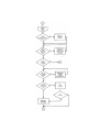
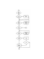
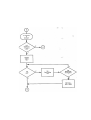
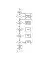
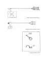
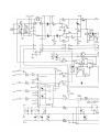
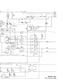
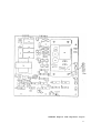
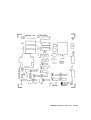
1
PRESTEL ADAPTER SERVICE MANUAL
Part No. 415,001
Issue 2
August 1984
Within this publication the term 'BBC' is used as an abbreviation for
'British Broadcasting Corporation'.
°Copyright ACORN Computers Limited 1984
Neither the whole or any part of the information contained in, or the
product described in, this manual may be adapted or reproduced in any
material form except with the prior written approval of ACORN
Computers Limited (ACORN Computers).
The product described in this manual and products for use with it, are
subject to continuous development and improvement. All information of
a technical nature and particulars of the product and its use (
including the information and particulars in this manual) are given by
ACORN Computers in good faith. However, it is acknowledged that there
may be errors or omissions in this manual. A list of details of any
amendments or revisions to this manual can be obtained upon request
from ACORN Computers Technical Enquiries. ACORN Computers welcome
comments and suggestions relating to the product and this manual.
All correspondence should be addressed to:Technical Enquiries
ACORN Computers Limited
Newmarket Road
Cambridge
CBS 8PD
All maintenance and service on the product must be carried out by
ACORN Computers' authorised dealers. ACORN Computers can accept no
liability whatsoever for any loss or damage caused by service or
maintenance by unauthorised personnel. This manual is intended only to
assist the reader in the use of this product, and therefore ACORN
Computers shall not be liable for any loss or damage whatsoever
arising from the use of any information or particulars in, or any
error or omission in, this manual, or any incorrect use of the
product.
This manual is for the sole use of- ACORN Computers' authorised
dealers and must only be used by them in connection with the product
described within.
ACORN is a trade mark of ACORN Computers Limited
First published 1984
Published by ACORN Computers Limited
CONTENTS
Page
1
INTRODUCTION
1
2
PACKAGING AND INSTALLATION
2
3
SPECIFICATION
3
4
DISASSEMBLY AND ASSEMBLY
4
5
CIRCUIT DESCRIPTION
5
6
DETAILED CIRCUIT OPERATION
7
7
FAULT FINDING ON THE PRESTEL ADAPTOR
11
APPENDIX A
De-bugging Program
17
APPENDIX B
Diagnostic Flowcharts
19
RS423 Cable Assembly Detail
Telephone Cable Assembly Detail
Speaker Assembly Detail
35
35
35
PRESTEL Adapter -
Block Diagram
Circuit Diagram
37
39
PCB Component Layout
PCB Silk Screen
41
43
Final Assembly
Case Lower Assembly
Wiring Diagram
45
47
49
Final Assembly
Case Lower Assembly
PCB Assembly
51
52
52
Parts Lists -
WARNING: THE PRESTEL ADAPTER MUST BE EARTHED
Important: The wires in the mains lead for the Prestel Adapter are
coloured in accordance with the following code:
Green and yellow
Blue
Brown
Earth
Neutral
Live
As the colours of the wires may not correspond with the coloured
markings identifying the terminals in your plug, proceed as follows:
The wire which is coloured green and yellow must be connected to the
terminal in the plug which is marked by the letter E, or by the safety
earth symbol or coloured green, or green and yellow.
The wire which is coloured blue must be connected to the terminal
which is marked with the letter N, or coloured black.
The wire which is coloured brown must be connected to the terminal
which is marked with the letter L, or coloured red.
If the socket outlet available is not suitable for the plug supplied,
the plug should be cut off and the appropriate plug fitted and wired
as previously noted. The moulded plug which was cut off must be
disposed of as it would be a potential shock hazard if it were to be
plugged in with the cut off end of the mains cord exposed. The moulded
plug must be used with the fuse and fuse carrier firmly in place. The
fuse carrier is of the same basic colour* as the coloured insert in
the base of the plug. Different manufacturers' plugs and fuse carriers
are not interchangeable. In the event of loss of the fuse carrier, the
moulded plug MUST NOT be used. Either replace the moulded plug with
another conventional plug wired as previously described, or obtain a
replacement fuse carrier from an authorised BBC Microcomputer dealer.
In the event of the fuse blowing it should be replaced, after clearing
any faults, with a 3 amp fuse that is ASTA approved to BS1362.
Exposure
Like most electronic equipment, the Prestel Adaptor should not be
exposed to direct sunlight or moisture for long periods.
*Not necessarily the same shade of that colour.
1. INTRODUCTION
This manual is intended to provide the information required to
diagnose and repair faults on the PRESTEL Adapter (a part of the BBC
Microcomputer system) which was designed by ACORN Computers Ltd., of
Cambridge, England.
The information contained in this manual is aimed at ACORN dealers and
service engineers who will be servicing the PRESTEL Adapter on behalf
of ACORN Computers Ltd.
2.
PACKAGING AND INSTALLATION
2.1 The BBC Microcomputer PRESTEL Adapter is supplied in a two part
moulded polystyrene packing which is further packaged within a
cardboard sleeve.
2.2 The following items are supplied with the PRESTEL Adapter:
PRESTEL ROM
PRESTEL Subscriber's Application Form
PRESTEL User Guide
PRESTEL Prompt Card for BBC Microcomputer Function Keys
Guarantee Registration Card
Voucher redeemable against replacement of a BBC
Microcomputer MOS ROM below version 1.0.
2.3 A mains power switch is located at the rear of the PRESTEL
Adapter.
2.4 A 400mA slow-blow type fuse is located at the rear of the unit.
Before removing this fuse, the PRESTEL Adapter must be disconnected
from the mains supply. Access to the fuse may be gained by undoing the
round cover with the slot in it using a screwdriver. The mains supply
must not be reconnected until the fuse is relocated in its holder and
the cover screwed home.
2.3 Do not use the PRESTEL Adapter in conditions of extreme heat, cold,
humidity or dust or in places subject to vibration. Do not block
ventilation under or behind the computer. Ensure that no foreign
objects are inserted through any openings in the adapter casing.
3. SPECIFICATION
The PRESTEL Adaptor
Interfaces a BBC Microcomputer to any British Telecom attached
1200/75 baud dial-up system (e.g. PRESTEL, MICRONET, TELECOM GOLD).
Operates with any BBC Microcomputer model B with 1.2 MOS or later
issue.
The unit is housed in a two part rigid injection moulded case,
containing a PCB carrying the following:
Modem
Auto-Dialler
RS232/423 compatible interface*
Telephone line interface
Power Supply
Mains on/off switch on rear panel
Call set-up and auto-dialler fully computer controlled. A 1200/75 baud
modem interfaces to the RS423 serial port on the BBC Microcomputer and
to the telephone line via the telephone line barrier. All data
processing is performed by software including the downloading of
telesoftware files from MICRONET 80.
Loudspeaker monitor during call set-up
Format:
C.C.I.T.T. V23
Speed:
(operating frequency)
Operating temperature:
1200 baud receive
75 baud transmit
10° - 35°C
Power In:
240v, 50Hz, lOw
13amp moulded-on plug
Signal Connections:
Cable to 5-pin DIN domino plug (RS423 interface)
Cable to BT series 400 line jack plug (telephone connection)
Complies with BS415 Class 1
British Telecom approval no.S/1462/3/D/021864
Dimensions: 7 70mm High 210mm Wide
350mm Deep
Weight: Unit onlyPacked-
1.5kg
1.7kg
*see page 6
3
4. DISASSEMBLY AND ASSEMBLY
1. In order to service the PRESTEL Adapter, first switch off and
disconnect it from the mains supply, also disconnect both the RS-423
cable and telephone connector (from the BBC Microcomputer and telephone
jack socket respectively).
2. The lid of the PRESTEL Adapter may be removed after undoing three
fixing screws, two on the rear panel, and one underneath. When
reassembling, press the lid down at the rear whilst tightening the two
rear fixing screws. Take care not to lose the two spire nuts pushed on
to the case lid into which the rear fixing screws locate.
3. Inside the PRESTEL Adapter are two sub-assemblies: the
printed circuit board and the speaker plate assembly.
4. The printed circuit board may be removed by the following
procedure:
(i)
Disconnect the RS-423 and telephone cables from the PCB by
removing the 9 faston tab connections at the rear of the board.
(ii)
Disconnect the two mains connection wires (blue and brown)
from the PCB.
(iii) Disconnect the twisted speaker cable from the PCB.
(iv) Undo the six fixing screws; the PCB may then be lifted clear.
5. The speaker plate assembly may be removed after the 6 retaining nuts
and bolts are unscrewed, and the speaker cable is disconnected from the
PCB.
5. CIRCUIT DESCRIPTION
1. This section should be read in conjunction with the block diagram
and, if necessary, the circuit diagram in the Appendix.
2. Modem
The modem circuitry is based around the Texas TCM3101 single chip
modem (IC1). It is a medium speed frequency shift keying (FSK) modem
which
contains
modulator/demodulator
and
signal
conditioning
circuitry, and is configured to operate on CCITT V23 standard
frequencies.
The modem will always accept input (RX) data at 1200 baud. The
Transmit data speed is selectable to either 75 baud or 1200 baud,
depending upon the state of TXT1 and TXT2 pins on IC1. In normal
PRESTEL mode, TXT1 will be at logic 1 and TXT2 will be at logic 0.
Considering only the 1200/75 mode of operation, i.e. transmit @ 75
baud, receive @ 1200 baud, the operation of the modem is as follows:
To transmit data the TXD input controls an output signal on the TXA
pin which is a sine wave of one of two distinct frequencies. A logic 0
on the TXD pin generates an output frequency of 450Hz, and a logic 1
will output a frequency of 390Hz. This signal is buffered through IC2
and fed to the telephone line via Tl, the line matching transformer.
Such signals are well suited to transmission through 'phone lines as
they are well within the bandwidth of the telephone system and contain
no high frequency harmonics.
Data is received from the telephone line, amplified through IC2 and
fed into the RxA input of the Modem. It is again in the form of a sine
wave, of one of two distinct frequencies. However, as the RxData rate
is 1200 baud, the two frequencies used as a standard are different. A
logic 0 appears as a 2100Hz frequency and a logic 1 as a 1300Hz
frequency. Circuitry internal to the modem conditions this signal and
outputs a logic 0 or 1 on the RxD pin (of IC1), depending on whether a
2100Hz or 1300Hz frequency is present at the input.
The CDT output of IC1 is a signal which becomes active if a valid
signal is present on the RxA input to the modem, i.e. a sinusoidal
signal. Its primary function is to indicate when communication between
the modem and an external device has been established.
3. RS423 Line Interface*:
This interface provides the interconnection between the PRESTEL
Adapter and the BBC Microcomputer. It translates the input signal
levels from +5 volts to +5v CMOS logic levels, and the converse for
output signals. It carries the Receive Data, Transmit Data, CTS (
Carrier Detect and Ring Indicator) and the RTS (PRESTEL Adapter
Control) signals.
5
4. Relay Drivers:
These are Darlington current drivers, contained in a single IC package
(IC11), controlled by CMOS logic. They are able to sink the high
current levels required to drive the relay coils.
5. Amplifiers:
The modulated data output and data input of the modem chip are
buffered by amplifiers (IC2). Also, the telephone line may be audibly
monitored through the loudspeaker, which is driven by the amplifier
IC5.
6. Control and Decode:
This section contains all the logic within the Adapter. Driven from
the main modem clock (frequency 4.43 MHz) the decode circuitry will
detect one of two pulses of a predetermined width, on the RTS input
line. The first type of pulse will cause all of the control circuitry
to be reset to its initial on-hook state. The second type of pulse may
then be repeatedly applied to the RTS line to step the control
circuitry through a series of control states. In this manner the
following control functions are provided:
(i) Modem Mode select (Transmit baud rates, Originate/Answer).
(ii) Activation of Line Seize, Dial-on and Digit Relays
(iii) Loudspeaker on/off state.
(iv) Control of CTS o/p line such that it provides the function of
Carrier Detect or Ring Indicator.
Also, in conjunction with the Transmit Data line, the Dial relays may
be controlled to generate the digits required for Pulse dialling.
7. PSU:
The power supply unit produces +5 volts at around 200mA and -5volts at
around 50mA. It requires a 240v, 50Hz AC mains input and is a linear
power supply circuit using three terminal regulators and a mains
transformer. The circuitry is protected by fuses on both positive and
negative output rails.
*Note: The Line Interface signal is RS232/423 compatible. The PRESTEL
Adapter 5-pin DIN 'domino' plug connects to the RS423 serial port on
the BBC Micro; for clarity, the interface signal is therefore referred
to as 'RS423' throughout this manual.
6
6. DETAILED CIRCUIT OPERATION
The operation of the PRESTEL Adapter is controlled by the RTS input
signal from the RS423 interface. A pulse of approx 2.35mSec width on
the RTS line will cause the internal circuitry to step through the
various control states shown in Fig. (i). This is called a "STEP pulse"
.
Fig. (i) PRESTEL Adapter State Diagram
A pulse of approx 1.41ms will be internally decoded as a "RESET pulse"
and will reset the PRESTEL Adapter to its 'offline' or initialised
state. Using these two pulse signals it is possible to configure the
Adapter to any one of the modes shown in Fig. (i).
Internal decoding of these pulses is accomplished by IC7 and IC9, these
are a 14-stage binary ripple counter and a 2-to-4 line decoder. The
counter, IC7, is. clocked by the stable 4.43 MHz crystal controlled
oscillator internal to the TCM 3101 Modem chip (IC1). The final two
stages of the counter, Q13 and Q14, drive the decoder. The sequence of
operation is as follows:
When a pulse is applied on the RTS input the counter IC7, is enabled (
RST, pin 11 goes low) and starts counting at 4.43 MHz, and continues to
do so as long as the pulse on RTS is active.
7
When the pulse goes low, Q13 and Q14 will be in a certain state,
dependent upon the width of the RTS pulse, and the decoder, IC9, will
be enabled, and will decode Q13, Q14 to produce an output on Q0 to Q3
of IC9. Only Q1 and Q2 of IC9 are used and they will produce a short
negative pulse under the following states:
(i)
(ii)
Step pulse (on Q2 of IC9) if Q13 low and Q14 high.
Reset pulse (on Q1 of IC9) if Q13 high and Q14 low. Any other
states on Q13 and Q14 are not recognised.
See Fig. (ii).
Fig. (ii) RTS-Pulse Timings
Note: Although the counter is reset as soon as the RTS pulse goes low,
i.e. all Q outputs of IC7 are set to zero, internal gate
delays allow the end count conditions on Q13, Q14 to be
decoded by IC9 before they are set to zero. This produces a
very short negative pulse on the Q1 or Q2 outputs of the
decoder (IC9).
These internal Step and Reset pulses from IC9 are used to generate the
control signals required to configure the states shown in Fig. (i).
These control signals are the outputs of two 4 bit binary counters (
IC10). The Reset pulse simply resets the main counter (on IC10, pin
15) such that all outputs are low, a power-on reset is also provided
by R16 and C31.
The Step pulse is applied to the clock inputs of IC10 to sequentially
enable/disable the control outputs (Q0 to Q3) in a binary count. These
outputs are gated through IC6 and IC8 to activate the relays, as
required in the correct sequence.
8
The output Q0 is a speaker on/off switch and can activate the line
seize relay. The output Q1 always activates the line seize relay. The
output Q2 always activates the line seize relay, provides modem mode
control, and, if LK3 is set, will disable the second of the two 4 bit
counters. The output Q3 always enables the line seize relay, and, if
LK3 is set as shown in the PCB assembly diagram, will enable the second
of the two 4 bit counters.
If the second of the two counters is enabled then the Q0 output of the
second counter provides additional mode control to the modem.
The link, LK3, is provided to enable a Transmit Data at 1200 baud mode
on the modem. It should always be set to enable this mode, as shown in
the PCB Layout on page 41 (items 73,74, LK3 fitted in position shown by
solid black area).
Normally, the link connects Q3 on the first counter to the Enable input
on the second counter and all states shown in Fig. (i) are available.
This is the default setting for LK3 for normal PRESTEL operation.
If LK3 is set such that Q2 is connected to the enable input of the
first counter, then Q3 is never clocked high thus keeping the second
counter in the reset state. The PRESTEL Adapter can therefore only step
through control states 1 to 8 [see Fig. (i)].
The operation of the relays in the telephone line interface is in the
following manner:
The Line Seize relay (RL1) is normally open and is activated (closed)
to seize the line to enable data transmission and dialling. To enable
the data link only RL1 need be on (closed).
To generate dialling signals the relays RL2 and RL3 operate as shown in
Fig. (iii). To dial a digit the Dial-on relay is closed and the Dial
Relay, RL3, is opened and closed the same number of times as the digit
to be dialled, with timings as shown in Fig. (iii).
IC8 allows the TxD line, from the RS423 interface to control the Dial
relay RL3, when the Dial-on-relay (RL2) is closed. Thus to dial a digit
the Dial-on relay needs to be closed and a series of pulses sent along
the TxD line with timings as shown in Fig. (iii).
The Ring Detector IC31 provides a logic 0 signal if a ringing signal is
detected on the telephone line whilst the Line Seize relay is open.
This signal is gated through to the CTS output on the RS423 interface.
The gates IC14 and IC8 control the CTS output such that it provides
both a Carrier Detect and a Ringing Detect output, depending upon the
state of the Line Seize and Dial-on relays. If the line is seized and
the Adapter is not dialling then the Carrier Detect output from the
Modem is gated onto CTS. If the line is not seized then the Ring
Detecter signal is gated onto CTS.
1
Not fitted to current production
9
Example
1.
2.
3.
4.
5.
shows the digits 3 and 2 being dialled
DIAL-ON RELAY SET-UP TIME
>5mS
BREAK PULSE WIDTH
66mS ±6mS
MAKE PULSE WIDTH
33mS ±3mS
DIAL-ON RELAY HOLD TIME
>5mS
INTER-DIGIT DELAY TIME
>850mS
Fig. (iii) Dial Characteristics Timing Diagram
10
7. FAULT FINDING ON THE PRESTEL ADAPTER
7.1 General
Any description or accompanying note giving details of the fault and
how it came about should be read carefully. Always ensure that there is
a fault with the hardware and that it is not due to the user's software
or the user's understanding of the PRESTEL Adapter which is the
problem.
Always check the power supply voltages on the PCB as a matter of
course. (See 'Power Supply Checks', page 15)
Also check all the fuses on the PCB itself; there are six PCB mounted
fuses which may become loose if the PRESTEL Adapter has been subjected
to excessively rough handling.
If a fault has to be traced through on the PCB, a useful debugging
program for the BBC Microcomputer is given in Appendix A. This routine
configures the function keys as follows:
f0
f1
f2
f3
f4
f5
f6
STEP PULSE
RESET PULSE
CONTINUOUS STEP PULSES
CONTINUOUS RESET PULSES
RL1 ON
RL2 ON
RL3 ON
Keys f2 and f3 may be used to trace the progress of a STEP or RESET
pulse through the decoding circuitry.
Keys f3, f4 and f5 will activate relays RL1, RL2 and RL3 respectively
so that their operation can be individually checked.
7.1 Fault Conditions
A PRESTEL Adapter failure can usually be related to one of the
following fault conditions:.
No PRESTEL display after entering *PRESTEL
This will occur if:
a) A PRESTEL ROM version 1.0 or higher has not been installed in the
BBC Microcomputer to which the PRESTEL Adapter is connected.
b) The PRESTEL ROM is not installed in the BBC Micro.
c) The PRESTEL ROM has failed.
11
Failure to recognise that the adapter is plugged in and switched
on.
This will be shown by the 'Adapter?' error message being displayed by
the BBC micro when dialling is attempted.
This may be the result of:
a) The RS423 connector inserted into the BBC microcomputer
socket incorrectly (the cut-out should be facing UP).
b) The Mains fuse in the rear of the Adapter blown.
c) Loose or faulty internal fuse (FS4).
d) Internal power supply circuitry faulty.
Failure to seize the telephone line.
This will be apparent by failure to hear the 'dial tone' through the
Adapter's speaker when dialling starts.
This may be the result of:
a)
b)
c)
d)
e)
Poor or incorrect connection to the telephone line socket.
Faulty speaker connections or speaker.
Internal power supply circuitry faulty.
Circuit fault.
Faulty relay (RL1)
Failure to dial correctly.
This will be apparant by failure to hear the dail relays within the
adapter clicking as dialling proceeds.
Note: this sound is weak, and the ear may need to be close to the
Adapter to hear it. It is produced by the mechanical action of the
relays opening and closing and is not heard through the speaker.
This may be the result of:
a)
b)
c)
d)
Loose or faulty internal fuse (FS1 and FS2)
Circuit fault
Internal power supply faulty
Faulty relay (RL2 or RL3)
Failure to establish a call to a PRESTEL Computer after correct
dialling.
This will be apparent by failure of the PRESTEL 'Welcome ' frame to
appear, failure of the 'online' message to appear at the bottom of the
screen, and no answer tone heard through the speaker once a telephone
connection is made.
This may be the result of:
a)
b)
c)
d)
e)
12
Loose or faulty internal fuse (FS3)
Modem IC1 faulty
Circuit fault
Internal power supply faulty
Incorrect number being dialled
No response to keyboard.
This may be the result of:
a)
b)
c)
d)
Power Supply faulty
Modem IC1 faulty
Circuit fault
BBC Micro fault
Diagnostic Flowcharts for the above conditions are given in Appendix B.
These should be read in conjunction with the following Circuit Checks:
Circuit Checks
It is assumed that the PRESTEL Adapter is connected to a BBC micro
installed with a PRESTEL ROM. The Adapter MUST NOT be connected to a '
phone line. The following equipment is also required:
I
II
20MHz oscilloscope, dual trace
DVM to measure ±5 volts to within ±0.01 volts
The function of the Adapter circuitry is to decode input pulses from
the RTS input and configure the 'phone line interface (relays) and
modem chip mode control as shown in the State Diagram, Fig.(i). A fault
in this circuitry may manifest itself in a number of ways, and could
give rise to any of the faults stated above.
The best method of checking through the circuitry is by exercising the
Adapter using the debugging program given in Appendix A (see above).
This program will configure the function keys to produce RESET and STEP
pulses, and to produce a continuous stream of either. The decode
circuitry may be checked by observing the progress of pulses sent
through the RTS line.
A continuous series of RESET pulses may be sent to the Adapter by
pressing the "RESET LOOP" function key, f3.
The path of the signal from the RTS input to pin 11 of IC7 should be
traced, using a 'scope. Triggering the 'scope on the rising edge of the
RTS input signal (use FS1), a second 'scope probe should be attached to
IC7 pins 2 and 3 in turn. Their states at the falling edge of the RTS
pulse should be as shown in the RTS-Pulse Timing Diagram, Fig.(ii), for
a 'reset' pulse.
Press ESCAPE and then press the "STEP LOOP" function key, f2.
Observe the signals on IC7 pins 2 and 3 again. Their states at the
falling edge of the RTS signal pulse should be as shown in Fig.(ii) for
a STEP pulse. If their states are incorrect, check the clock input, IC7
pin 10. This should be a continuous 4.43 MHz clock signal. (Note: this
is a fairly fast signal for CMOS logic and slow edges to the clock
signal are to be expected ). If this
13
is not present, check IC6 pin 8, where the clock should also be seen,
and that IC6 pin 9 is at a logic 0. This signal goes to a logic 1 only
when the RTS input is held continuously high, thus disabling the clock
input; short pulses such as STEP and RESET pulses on the RTS input will
not affect it.
If the clock is still not present then check for open circuits / track
shorts around the crystal XTAL1 and its connections.
To continue checking the decode circuitry, set the 'scope to trigger
the falling edge of the RTS input pulse and observe the signal on IC9
pin 6. This should be a very short negative pulse of not less than 250
nSec (note: this is a single short pulse that occurs every few
milliseconds so a high level on the 'scope intensity and a fast
timebase is required to observe it). It is this pulse that is used as a
clock input to step through the counter IC10 whose outputs control the
Adapter state (see Fig.i).
If the "RESET LOOP" is again applied to the adapter (f3) a similar
signal should be seen at IC9 pin 5. Ensure that this pulse is also
present at IC10 pin 15. If it is not check that IC12 pin 6 is at a
logic 1; this input is a power-on-reset signal which should be high at
all times.
To check the action of the counter:
From the reset state, repeatedly press the "CALL STEP" function key (
f0), and observe the counter outputs from IC10, pins 11,12,13 and 14.
These outputs should perform a binary count from 0 through to 8 (binary
1000), as each STEP pulse is applied from the f0 function key. Once it
reaches a count of 8, then further STEP pulses should have no further
effect on the counter. However, further STEP pulses after a count of 8
should then start to cause the signal on IC10 pin 3 to toggle between 0
and 1. If the link LK3 is in the wrong position, then the counter
outputs from IC10 will only count up to binary 4 and IC10 pin 3 will be
permanantly low.
To check the action of the relays:
The debugging program given in Appendix A configures the function keys
f4, f5, f6 to activate RL1, RL2 and RL3 respectively. Thus alternately
pressing the respective function key and f1 (RESET) will cause that
relay to open and close. This sound should be audible and is a way of
checking their operation. However, the contact resistance of each one
should also be checked with a meter.
RL1 may be checked for operation by alternately pressing the f4 key and
the f1 key. Using the 'scope observe IC11 pin 13, which should be
switching between 0 and 1 (note: its logic 0 output may be up to 1
volt). Also listen carefully and the mechanical action of the relay
opening and closing should be heard. If the signal is switching but no
clicking is heard, check the resistance between the connections A and C
at the 'phone cable connections at the rear of the pcb. It should be
alternating between open circuit ( >1 Mega ohm) when open and less than
100 ohms when closed. If this is not so then replace RL1.
For RL2 press the f5 function key. The resistance across the A and C
terminals should be less than 25 ohms.
14
For RL3 press the f6 function key. The resistance across the A and C
terminals should be >1 Mega ohm with RL3 active.
If any of these are incorrect then replace the appropriate relay
To check the operation of the modem chip IC1:
Pin 10 is the Carrier detect level adjustment and is set by R19 and
R20 to be a constant 3.2 volts ± 0.2 volts. Pin 7 is the Receive bias
adjustment and is set by R18 and R20 to be a constant 2.7 volts ± 0.2
volts. If either of these are incorrect then data transfer problems
may be encountered. Check and replace resistors if necessary. Pin 3 is
the Carrier Detect output and is low in the RESET state. Providing 9
STEP pulses will switch the output to a logic 1. If this does not
occur a fault exists within the modem chip IC1, or in the line
amplifiers circuitry. Pin 13 and 12 are the modem mode control inputs,
TXT1 and TXT2. They should both be a logic 1 on reset. After 4 STEP
pulses the modem will be configured to a transmit at 75 baud mode and
pin 12 will go low. Step 8 takes it to the Recieve at 1200 baud mode
and pin 12 returns high. Subsequent STEP pulses will toggle both pins
12 and 13 between logic 0 and 1. The modem chip modes for combinations
of these two inputs are:
TXT1
0
0
1
1
TXT2
0
1
0
1
Modem IC mode
Tx
Tx
TX
Rx
at
at
at
at
1200 (1200/1200)
600
(not used)
75
(1200/75)
1200 (1200/1200)
Pin 11 is the Transmit analog output. It is the modulated output
corresponding to the state of the TXD input pin (14).
Power Supply Checks
Before examining signals on the PCB it should be ensured that the
power supply is providing the correct voltages. Use a DVM to ensure
that TP9 is at +5 volts (±100mV), and that TP7 is at -5volts (±200mV).
Also check that this voltage is present across fuses FS5 and FS6
respectively (a drop of up to 0.1 volt across each fuse may be
expected). If a fuse has blown the Adapter should be switched off and
the fuse replaced. If it continues to blow, check for short circuits
on the pcb.
If the voltages are not within specification, then the PSU circuitry
may be checked as follows.
Firstly, disconnect the Adapter from the mains supply. Remove the 6
screws securing the PCB, and disconnect the speaker. Remove the 4 M3
bolts, washers and nuts securing the plastic enlosure covering the PSU
components.
If the voltage on one of the Test Points is only slightly out of spec.
then the voltage regulator associated with that voltage is suspect and
should be replaced, e.g. IC15 for the +5 volt rail, and IC16 for the 5 volt rail.
15
Reposition the PCB in the lower case, ensuring that no washers, bolts
etc. have been left in the base, and switch on the Adapter. Using a '
scope, observe the "15V" pin protruding from the PSU transformer to
check for a 15 volt AC waveform. If it is not present, then disconnect
from the mains and check the continuity of the mains wiring from cable
to PCB. If this is OK then replace the transformer. If the 15 V AC is
present, check the (+)ve terminal of C34 for a DC voltage of +20 volts
with up to a 15 volt peak-to-peak ripple. If the voltage is incorrect
then replace the bridge BR1 and the regulator IC15. Repeat this for
the negative rail by checking that the voltage at the (-)ve end of C37
is at -22 volts with up to a 5 volt peak-to-peak ripple. If not then
replace BR1 and IC16.
If a fault still persists, then check for short and open circuits
around the PSU circuitry.
16
APPENDIX A - PRESTEL Adapter Debugging Program
for the BBC Microcomputer model B
10
20
30
40
50
60
70
80
90
100
110
120
130
140
150
160
170
180
190
200
210
220
230
240
250
260
270
280
290
300
310
320
330
340
344
350
355
360
370
380
390
400
410
420
430
440
450
460
470
480
490
500
510
520
REM
REM
REM
REM
REM
This listing configures the
function keys f0 and f1 to
generate "STEP" and "RESET"
pulses to assist debugging of
PRESTEL Adapters.
REM Note: this routine expects a
REM PRESTEL ROM to be installed.
UARTS=&FE08
RTSHTXDH=&6A
RTSHTXDL=&0A
DIMQ%l00
FOR I%=0 TO 2 STEP 2
P%=Q%
[ OPT I%
\
.XSTEP
LDA #1
JMP OSWORD
\
.XRESET
LDA #0
\
.OSWORD
STA PB
LDX #PB MOD 256
LDY #PB DIV 256
SEI
LDA #&7B
JSR &FFF1
CLI
RTS
\
.RL1ON
JSR XRESET
JSR XSTEP
JMP XSTEP
\
.RL2ON
JSR RL1ON
LDA #RTSHTXDH
STA UARTS
RTS
\
.RL3ON
JSR RL20N
LDA #RTSHTXDL
STA UARTS
RTS
\
.PB EQUB 0
\
]
17
530
550
560
570
580
590
591
592
593
600
610
620
630
640
641
642
643
650
18
NEXT 540. PRINT
PRINT"FUNCTION KEY CONFIGURATION:_"
PRINT"f0...CALL STEP"
PRINT"f1...CALL RESET"
PRINT"f2...STEP LOOP"
PRINT"f3...RESET LOOP"
PRINT"f4...CALL RL1ON"
PRINT"f5...CALL RL2ON"
PRINT"f6...CALL RL3ON"
PRINT
*K.0 CALL XSTEP|M
*K.1 CALL XRESET|M
*K.2 REPEAT:CALL XSTEP:UNTIL 0|M
*K.3 REPEAT:CALL XRESET:UNTIL 0|M
*K.4 CALL RL1ON M
*K.5 CALL RL2ON M
*K.6 CALL RL3ON M
END
APPENDIX B
DIAGNOSTIC FLOWCHARTS
The letters in circles refer
to the relevant flowcharts
which follow.
Master Flowchart
19
RS423 Cable Assembly Detail
Telephone Cable Assembly Detail
Speaker Assembly Detail
35
PRESTEL Adapter PCB Component Layout
41
PRESTEL Adapter PCB Silk Screen
43
PRESTEL Adapter Final Assembly
PRESTEL Adapter Case Lower Assembly
47
PRESTEL Adapter Case Lower Assembly Wiring Diagram
49
PRESTEL ADAPTER PARTS LISTS
NOTE:
Items indentified by * are normally available as spare
parts - please contact your supplier for details of
availability.
+ denotes SAFETY CRITICAL COMPONENT - see below
IMPORTANT
In order to comply with BT approval regulations, components used within
this unit must only be replaced with exact equivalent parts. All
replacement parts identified in the list below are deemed to be "Safety
Critical" and must be obtained from the Customer Services department of
Acorn Computers Limited. On no account may any other part be
substituted. Failure to comply with this may result in a breach of
approval regulations and may cause the product to became unsafe.
SAFETY CRITICAL COMPONENTS
ACORN PART NO.
DESCRIPTION
810,005
810,004
810,003
865,002
RELAY
RELAY
RELAY
BARRIER TRANSFORMER
ITEM PART No.
DESCRIPTION
QTY REMARKS
PRESTEL Adapter Final Assembly (SEE PAGE 45)
3
4
5
7
8
10
11
SEE BELOW
201,109 *
201,182 *
882,946 *
882,665
201,183
2
4
5
12
13
14
17
835,001 *
800,082
800,080
882,022
882,902
882,972
890,000 *
CASE ASSEMBLY,LOWER
CASE MOULDING,UPPER
LABEL, CASE, UPPER
NUT,SPIRE No.6
SCREW, No.6 x 13mm SELFTAP PAN HD
PLATE, SPEAKER FIXING
SPEAKER ASSEMBLY (SEE PAGE 35)
LOUDSPEAKER, 16 OHM, 0.2W
SHELL, 2 WAY
CONNECTOR, CRIMP
SCREW, M3 x 8mm SL CH HD SCR
NUT, M3 HEX. FULL
WASHER, M3 INT.TEETH
FOOT, 'STICK-ON'
1
1
2
3
1
BLACK
1
1
2
6
6
4
51
ITEM
PART No.
DESCRIPTION
QTY REMARKS
PRESTEL Case Lower Assembly (SEE PAGES 47 & 49)
2
4
5
7
8
9
10
12
14
15
16
17
20
23
25
26
27
28
201,110 *
882,652
805,003
815,900
815,209
815,901
201,184
201,185
880,026
880,025
201,186
201,187
880,101
201,188
201,189
201,190
201,191
*
*
*
*
*
CASE MOULDING, LOWER
PCB ASSEMBLY
SCREW, No6 x 6mm SELFTAP
SWITCH, MAINS
HOLDER, FUSE
FUSE 20mm x 5mm 400mA TYPE T
SHROUD, FUSE HOLDER
LABEL, REAR
CABLE, MAINS, C/W PLUG
GROMMET, TELEPHONE CABLE
GROMMET, MAINS/RS423 CABLE
CABLE ASSEMBLY, TELEPHONE
CABLE ASSEMBLY, RS423
TIE, CABLE
JUMPER, NEUTRAL
JUMPER, LIVE
STRAP, EARTH
JUMPER, FUSE
1
6
1
1
1 SLO BLO
1
1
1
1
2
1
1
4
1
1
1
1
PRESTEL PCB Assembly (SEE PAGES 41 & 43)
3
4
5
6
7
8
9
10
11
12
13
14
15
16
17
18
20
21
22
23
24
25
26
27
28
29
30
35
36
37
52
502,154
502,100
502,101
502,471
502,561
502,102
502,222
502,103
502,123
502,472
502,473
502,823
502,104
502,124
502,474
581,103
629,010
680,002
628,101
651,224
632,047
670,222
620,047
636,010
622,100
639,221
628,221
795,005
795,012
795,003
*
*
*
*
RESISTOR 150K
¼W 5%
RESISTOR 10R
¼W 5%
RESISTOR 100R
¼W 5%
RESISTOR 470R
¼W 5%
RESISTOR 560R
¼W 5%
RESISTOR 1K
¼W 5%
RESISTOR 2K2
¼W 5%
RESISTOR 10K
¼W 5%
RESISTOR 12K
¼W 5%
RESISTOR 4K7
¼W 5%
RESISTOR 47K
¼W 5%
RESISTOR 82K
¼W 5%
RESISTOR 100K
¼W 5%
RESISTOR 120K
¼W 5%
RESISTOR 470K
¼W 5%
POTENTIOMETER 10K PRE-SET
CAPACITOR 10nF PLATE CERAMIC
CAPACITOR 47nF/33nF DECOUPLER
CAPACITOR 100nF DISC CERAMIC
CAPACITOR 220nF DISC CERAMIC
CAPACITOR 47pF MIN. PLATE
CAPACITOR 2µ2 250V
CAPACITOR 0µ47 25V ELECT. AXIAL
CAPACITOR 0µ1 40V ELECT. AXIAL
CAPACITOR 10µ 16V ELECT. AXIAL
CAPACITOR 220µ 63V ELECT. AXIAL
CAPACITOR 220pF 63V MIN. PLATE
DIODE BZY96C5V1
DIODE BZX70C12
DIODE BZX79C3V3
1
1
1
1
1
2
2
1
1
1
1
2
1
1
1
1
2
17
2
2
2
2
2
2
3
1
1
4
4
2
R3
R12
R4
R8
R2
R13,17
R14,15
R11
R6
R11
R7
R1,22
R5
R9
R16
VR4
C2,4
C30,31
C1,3
C9,10
C5,29
C34,37
C32,35
C21,25,7
C33,36
C38
D3,4,5,6
D7,8,9,10
D1,2
ITEM
PART No.
DESCRIPTION
QTY
REMARKS
1
1
1
1
1
1
1
1
2
1
2
1
1
1
1
1
1
1
1
1
5
1
12
9
2
2
1
2
1
1
1
4
8
4
4
1
1
1
1
BR1
IC1
IC2
IC13
IC16
C15
IC5
IC4
IC6,14
IC7
IC8,12
IC9
IC10
IC11
XTAL 1
T1
T2
RL1
RL2
RL3
FS1,2,3,4,6
FS5
PRESTEL PCB Assembly (SEE PAGES 41 & 43) - cont'd
40
42
43
45
46
47
48
49
50
51
52
53
54
55
57
59
60
61
62
63
66
67
68
70
71
72
73
74
76
79
80
83
84
85
86
87
88
89
90
798,101
763,101
770,062
733,691
779,001
778,006
770,386
754,049
754,071
754,020
754,081
754,556
754,520
772,003
820,043
865,002
865,001
810,003
810,005
810,004
815,016
815,003
815,910
800,200
800,203
800,250
800,051
800,070
885,103
800,108
800,116
882,972
882,962
882,902
882,122
505,683
505,393
505,563
505,333
*
*
*
*
*
*
*
*
*
*
*
*
*
*
*
+
*
+
+
+
*
*
BRIDGE RECTIFIER 1KAB10
INTEGRATED CIRCUIT TCM3101
INTEGRATED CIRCUIT TLO62
INTEGRATED CIRCUIT DS3691
INTEGRATED CIRCUIT LM320LZ5
INTEGRATED CIRCUIT LM341P5
INTEGRATED CIRCUIT LM386
INTEGRATED CIRCUIT 4049B
INTEGRATED CIRCUIT 4071B
INTEGRATED CIRCUIT 4020B
INTEGRATED CIRCUIT 4081B
INTEGRATED CIRCUIT 4556B
INTEGRATED CIRCUIT 4520B
INTEGRATED CIRCUIT ULN2003A
CRYSTAL 4,433619 MHz
TRANSFORMER, BARRIER
TRANSFORMER, MAINS
RELAY
RELAY
RELAY
FUSE, 20mm x 5mm, 63mA TYPE F
FUSE, 20mm x 5mm, 250mA TYPE F
HOLDER, FUSE, PCB MTG
FASTON TAB, 0,110"
FASTON TAB, O,250"
PIN, 2 WAY
PIN, 3 WAY
SHUNT
PLASTIC BOX
SOCKET, I.C., 8 WAY, DIL
SOCKET, I.C., 16 WAY, DIL
WASHER, M3, SHAKEPROOF
WASHER, M3, PLAIN
NUT, M3, FULL
SCREW, M3 x 6mm PAN HD
RESISTOR 68K ¼W 2%
RESISTOR 39K ¼W 2%
RESISTOR 56K ¼W 2%
RESISTOR 33K ¼W 2%
LK1
LK3
LK1,LK2
FOR IC1
R21
R18
R20
R19
53