1
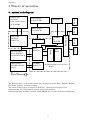
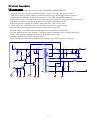
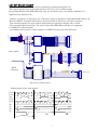
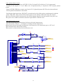
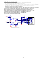
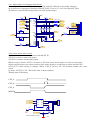
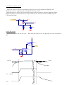
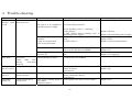
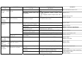
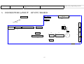
ELECTRONIC CASH REGISTER
G356E
SERVICE MANUAL
DOCUMENT No. 5140-02-03
REV.01
TITLE : G356E SERVICE MANUAL
PREPARED BY
K. SAKAUE
2004/4/21
APPROVED BY
COPY RIGHT
2004 BY JAPAN CASH MACHINE CO., LTD.
1
TABLE OF CONTENTS
1 Introduction ..................................................................................................................................................................1
2 Installation procedure..................................................................................................................................................1
2.1 unpacking ..............................................................................................................................................................1
2.2 Emergency cash drawer release...........................................................................................................................3
2.3 Preparation for use .............................................................................................................................................3
Dip switch setting....................................................................................................................................................3
Initial reset procedure.............................................................................................................................................3
Diagnostics...............................................................................................................................................................4
3 Theory of operation ......................................................................................................................................................5
3.1 system block diagram............................................................................................................................................5
3.2 circuit description..................................................................................................................................................6
3.2.1 power circuit ...................................................................................................................................................6
3.2.2 KEY BOARD CIRCUIT..................................................................................................................................7
3.2.3. display circuit ................................................................................................................................................8
3.2.4. printer drive circuit .......................................................................................................................................9
3.2.5. Comparator circuit ........................................................................................................................................9
3.2.6 Paper near end sensor circuit ......................................................................................................................10
3.2.7. Motor drive circuit(paper feed motor) ........................................................................................................ 11
3.2.8 cutter motor drive circuit ............................................................................................................................. 11
3.2.9. Battery charge circuit..................................................................................................................................12
3.2.10. PF circuit....................................................................................................................................................12
4 Trouble shooting ......................................................................................................................................................15
5 CONNECTOR LAYOUT OF CPU BOARD .........................................................................................................17
5.1 CONNECTOR TABLE......................................................................................................................................18
5.2 Standard inner cable pin assignment ................................................................................................................19
5.3 Optional cable pin assignment ...........................................................................................................................19
6 Appendix .....................................................................................................................................................................20
2
1 Introduction
G356E consist of 5 block
(1)Main CPU board
Main CPU:M16C/80
Renesas device 16 bit
MPU
RAM 4M bit (battery back up)
EPROM 4M bit CMOS
(2)
(3)
(4)
(5)
Front display unit
Rear display unit
Key board unit
Power supply unit
2 Installation procedure
2.1 unpacking
The ECR packing method is shown fig 2-1.
Unpack the ECR an check that the following items are present.
(1) two rolls of thermal rolls 38mm
(2) one journal Take-up reel
(3) key set
(4) G356E owners manual
(5) Dust cover
If the ECR was received in a damaged carton, unpack and inspect for physical damage immediately,
As described in table 2-1. If damage is found, contact the freight carrier and file a claim promptly,.
If any parts are missing, contact JCM within one week of receiving the ECR.
Initial inspection
Perform the appearance and mechanical checks as listed on table 2-1.
The ECR cabinet can be detached by removing the three screw on the upper side of the cabinet.
The two screw is on the printer side. And other one is under the customer display unit.
It is concealed under a small cover.
Table 2-1
Check List
Inspection
Appearance
Mechanical
check
A. surface of cabinet , keyboard, and cash drawer for damage
such as dents and scratches.
B. display windows for damage such as
cracks or scratches.
A.
all electrical connections for proper seating
B. keys in mode lock for proper operation.
C. Cash drawer for smooth operation when released manually.
See selection 2.3 for release details.
1
2
2.2 Emergency cash drawer release
In the unlikely event of a machine malfunction or a prolonged power failure, the model G356E is
equipped with an emergency cash drawer release.
The release is located on the rear underside of the cash drawer. To manually release the drawer,
carefully lift one side of the ECR with your left hand and push the release tab with the other.
Rear
release
BOTTOM
VIEW
FRONT
FIGURE 2-2
2.3 Preparation for
Emergency Drawer Release
use
Dip switch setting
Dip switch is located on the front right corner of the main PCB.
It is used for initialization and hardware configuration purposes.
1: ON
initial reset
OFF
normal operation
Initial reset procedure
(a) Initial reset
(1)set DIP sw1 to ON.
(2)Power ON.
Clears RAM work area only (current transaction)
Does not effect totals/counters or program memory.
Operation mode become “P” mode.
(b) RAM clear(all clear)
(1)Turn the mode lock key to the “P”mode.
(2)Set DIP sw1 to ON
(3)Power ON while depressing the tenkey ”1”.
(4)All clear is displayed.
Clears all Totals/counters and user programmed memory. Loads default operation program
After all clear operation, you must preset the date and time in “X” mode.
The machine does not work without setting date and time.
3
Diagnostics
(1) turn the mode lock key to “P” position, or assign to “P” mode(4---key).
(2) Enter xxxxxxxxx(9digit) --- #/NS
555555555-----#/NS automatic receipt issue at 3 minutes interval.
555555551-----#/NS automatic receipt issue at 5 second interval without cutter.
555555552-----#/NS automatic receipt issue at 5 seconds interval with cutter.
666666666-----#/NS communication port loop back test
check the com. Port from 1 to 4.
Following result message is printed
Error2 RTS---CTS
defect
Error4 RxD ---TxD defect
777777777-----#/NS
automatic printing test
All characters are printed on receipt and journal automatically.
You can do a check of printing quality.
It’s terminated by depressing “CL” key
888888888-----#/NS
key board test
the display will show the each key s position number on the right side 2 digit
various signal status will be showed each digit on the display.
It’s terminated by depressing “CASH” key.
For example(display)
P 1 0 1 0 1 1 4 5
Key position code
Journal near end sensor
Receipt near end sensor
Journal paper empty
Receipt paper empty
Head up switch
Control key position
999999999-----#/NS
version and check sum display
The software version number and checksum of EP-ROM will displayed.
For example(display)
1 - 0 0 E F 1 0 3
check sum
destination spec.
Version number
4
Section 2
3 Theory of operation
3.1 system block diagram
Rear display
9 digits(VFD)
SCOM1
Printer unit
LTP 2w47
Cutter unit (option)
ACU1224B0
DRAWER
SCOM2
Front display
9 digit(VFD)
POWER
CIRCUIT
4M
RAM
SCOM4
MPU
M16C/80
SCOM3
SWITCHING
POWER SUPPLY
(+24V)
VFD driver
E-PROM
KEY BOARD
9 X 8 MATRIX
CONTROL LOCK
DRAWE
R
DRIVER
232C DRIVER
PRINTER
DRIVER
CIRCUIT
SCOM3,SCOM4 are reserved
MAIN
The ECR circuitry can be broken down into six major sections: MPU, Memory, Display,
Key board, Printer, and power supply.
The heart of this system consists of a M16C/80, Sixteen bit microprocessor
implementing L.S.I, high speed, and low power consumption.
Standard memory includes a 512k x 8 bit EPROM and a 512k x 8 bit static RAM chip.
5
3.2 circuit description
3.2.1 power circuit
POWER VOLTAGE (+5V,-30V,VEE,,VF1,VF2) REGULATOR CIRCUIT
After passing through the switching regulator. There is a +24V DC power via JP1.
This power supply circuit employs fly back converter type switching regulator system.
At the initial condition, as the level of point “I” is 0V, PQ4 keeps OFF condition.
When +24V begins to rise up after power ON, the level of point “H” rises up and PQ1 turns ON.
And then the power is applied to primary side of pulse transformer (PT1).
When the power is applied to primary side of the PT1 , the level of point
“I” (secondary side of the PT1 ) rises up, and if it is exceed the zenner voltage
of PD11(+5V), PQ4 turns on and the level of point “H” becomes 0V.
Therefore PQ1 is in OFF condition and supplement to primary input of PT1
is cut off, with that the level of point “I” becomes initial condition again and PQ1 turns ON.
Thus , switching the supplement of power to primary side of PT1,
secondary output(+5V,-30V,VF1,Vf2) is stable.
The +24V DC pass through u1(LM2575S-5.0 voltage regulator)become Vcc-c steady.
PC7
+24V
PR4
68
682
PD20
PC6
S1B-SB
PR7
PC16
22K
1000u
35V
PR3
PT1
S097866
5
6
PD12
PC18
RS1B_R8
PD9
3.3K 1/4W
PR6
15K
10V
PC10
10V
0.1U 220 1/4W
1000U
PS_+5V
DSS310
PC12
100U
7
PR5
PNF3
PR11
C20
0.1U
HZ36CPB 223K
PD10
HZU12B2
1
10
PQ3
2SC3052
PR8
50V
100u
9
PD8
RS1B_R8
1.5K
PD13
PL3
2
PQ1
BLM21PG600
0.1u
HZU5.1
2SC3568K
PC9
PR9
680
I
PC22
100p
3
PC8
102
100V
PD14
HZU5.1
8
2.2U
50V
VF1
PC21
PR10
330 1/4W
PQ4
2SC3052
PC11
50V
-30V
100U
PC19 PR12
0.1U 10K
RS1B_R8
22K
PD11
PC13
PC24
1000p
PC23
100p
VF1
PL4
4
BLM21PG600
PR13
3.3K 1/4W
H
6
3.2.2 KEY BOARD CIRCUIT
Input and output signal for key board scanning are passing through J1,J2
The output signals from output port (P110-P113) of U17 are encoded signals.
By passing through U25,U26(74HC138), they are decoded to key scan signals. And they are
applied to key matrix via J1.
When a certain key is depressed, one of decoded signal is applied to buffer(U20:74HC245) via J2.
Thus U17(MPU) recognizes which key is depressed and executes key’s specific operation.
The scanning signals are also used for digit indicator signals for display tube as well.
The scanning signal from U26 –Y0 scans control lines KR0-KR4 and they are applied to
U17(MPU) as control signals.
According to the status of control signals, U17(MPU) executes specific operation.
1
+5V
J1
U25
1
2
3
2
3
4
5
P110
P111
P112
P113
A
B
C
+5V
6
4
5
RA12
RA5-103J
G1
G2A
G2B
15
14
13
12
11
10
9
7
Y0
Y1
Y2
Y3
Y4
Y5
Y6
Y7
D1
D2
D3
D4
D5
D6
D7
D8
D9
1
2
3
4
5
6
7
8
9
KS0
KS1
KS2
KS3
KS4
KS5
KS6
KS7
KS8
74HC138
W-D0809#01
1
+5V
Scan signal
U26
1
2
3
6
4
5
D[0-7]
A
B
C
G1
G2A
G2B
15
14
13
12
11
10
9
7
Y0
Y1
Y2
Y3
Y4
Y5
Y6
Y7
CA1
J2
RA13
KR0
KR1
KR2
KR3
KR4
KR5
KR6
KR7
/LOCK
9
8
7
6
5
4
3
2
2
3
4
5
6
7
8
9
KR0
KR1
KR2
KR3
KR4
KR5
KR6
KR7
1
2
3
4
5
6
7
8
74HC138
EXF-P8101
MPU
Data bus
1
RA9-473J
U20
+5V
/CS1
D0
D1
D2
D3
D4
D5
D6
D7
1
19
2
3
4
5
6
7
8
9
W-D0808#01
DIR
G
A1
A2
A3
A4
A5
A6
A7
A8
B1
B2
B3
B4
B5
B6
B7
B8
18
17
16
15
14
13
12
11
KR0
KR1
KR2
KR3
KR4
KR5
KR6
KR7
D10
KR0
KR1
KR2
KR3
KR4
/LOCK
J3
1
2
3
4
5
6
CONTROL LOCK
5267-06
Fig 3-1 key board circuit
Timing chart of key scan signals
P110
P111
112
P113
P114
Y0
Y1
Y2
Y7
5.48msec
7
3.2.3. display circuit
Display signals are applied to the display circuit board via J4..
The display signals for digit indication are also used for key scan signals which are decoded
At U25,U26(VHC138). The decoded signals from U25,U26 are amplified at U23,U24(driver:uPA80C)
and applied to the display tube on display circuit board.
The display signals for segment indication are output from port of CPU(P150-P157,P76,P77).
They are amplified at U22,U23 (driver:uPA80C) and applied to the display tube on display circuit
board.
U22
7
6
5
4
3
2
1
SEGA
SEGB
SEGC
SEGD
SEGE
SEGF
SEGG
-30V
8
I7
I6
I5
I4
I3
I2
I1
O7
O6
O5
O4
O3
O2
O1
VSS VCC
L1
L2
L3
L4
L5
L6
L7
10
11
12
13
14
15
16
9
C70
UPA80C
VF1
+5V
1
2
3
4
5
6
7
8
9
10
11
DET1
VF1
SEG K
SEG P
SEG G
SEG F
SEG E
SEG D
SEG C
SEG B
SEG A
0.1u
U23
7
6
5
4
3
2
1
SEGP
SEGK
SEGL
DG8
DG7
-30V
8
I7
I6
I5
I4
I3
I2
I1
O7
O6
O5
O4
O3
O2
O1
VSS VCC
L8
L9
10
11
12
13
14
15
16
L10
L11
9
C69
UPA80C
+5V
0.1u
U24
7
6
5
4
3
2
1
DG6
DG5
DG4
DG3
DG2
DG1
DG0
-30V
8
I7
I6
I5
I4
I3
I2
I1
O7
O6
O5
O4
O3
O2
O1
VSS VCC
UPA80C
L12
L13
L14
L15
L16
L17
L18
10
11
12
13
14
15
16
9
C59
+5V
0.1u
VF2
DISP SW
12
13
14
15
16
17
18
19
20
21
22
23
24
25
26
DG8
DG7
DG6
DG5
DG4
DG3
DG2
DG1
DG0
VF2
DET2
DISPLAY DRIVE CIRCUIT
26FE BT-VK-N
8
3.2.4. printer drive circuit
Printer drive circuit consists of CPU(U17),U11,U12 and U9,U10 (driver), U13 (comparator)
Usually, P142 outputs “L” level. When one of department key is depressed, CPU outputs printer
power
Signal “H”(PR_PWR) from output port P142 of U17. Q3and Q4 turn ON. Thus the thermal head
On the printer mechanism is activated.
Serial print data input from “PR_DAT” is transferred to the shift register synchronously with the
Clock ”PR_CLK”, then stored in the latch register at the timing of the latch ”PR_/LA” signal.
The heat elements which correspond to the latched print data are activated while each gate is on.
The gates are on while each head activation signal (DST1 –DST4) is low.
3.2.5. Comparator circuit
The thermal head has a thermistor for detect the head temperature.
The level of the “TH_IN” is changed according to head temperature.
When head is heated too high temperature, the output level of comparator goes to “H” level.
Thus thermal head will be non-activity.
This status is released when the head become cool.
+24V
R27
50V
100u
10K
Q3
R28
2.2K 1/2W
2SB1100
L26
3
C31
Q4
DTC143EUA
2
1
J7
PR_PWR
1 VP
2 VP
3 VP
4 VP
5 DATA OUT
6 CLK
7 LATCH
8 DST2
9 DST1
10 TH
11 GND
12 GND
13 GND
14 GND
15 GND
16 GND
17 GND
18 GND
19 GND
20 GND
21 VDD
22 DST4
23 DST3
24 DATA IN
25 VP
26 VP
27 VP
28 VP
U12B
U12C
4
L27
3 6
74VHC14
U12A
L28
2
5
1 8
74VHC14
L29
+5V
9
PR_/LA
74VHC14
U11A
TH_IN
PR_CLK
74VHC14
U12D
1
3
PR_/DST1
2
74VHC32
PRGND
+5V
U11B
L20
L31
4
6
PR_/DST2
5
74VHC32
U12E
L30
U12F
10
11
12
74VHC14
13
74VHC14
28FE-BT-VK-N
4.7K
4.7K R39
TH_IN
47K
U13A
2
1
R40
+5V
R42
4
R38
3
2.2K
LM393
R41
R43
8
+5V
47K
220K
9
+5V
PR_/DAT
C
0
3.2.6 Paper near end sensor circuit
This circuit detects paper near end of receipt and journal individually.
The sensor is consist of a LED and a photo transistor.
It attached under the bottom base. There are two windows in order to sense the roll paper,
The light from LED reflect at the paper and be returned to the photo transistor.
Thus sensor output level become “H”(about 4V)
If paper roll slip out from holder, the light from LED cannot reflect, so the photo transistor
cannot receive the return light. Thus sensor output level become “L”(about 0.3V)
There is transistor on the CPU board in order to amplify the inputted signal.
So the inputted signal is not stable, that Q7,Q8 amplify the signal to “0V” or “5V”.
If paper roll slip out from holder, JNEND or RNEND will become to 5V.
When paper roll is on the holder, JNEND or RNEND is “0V”.
R72,R73 limit the current to supply to LED.
+5V
4.7K
3
+5v
R74
RNE
C61
Q7
DTC114EUA
0.1u
2
R73
4.7K
3
JNE
330
330
Q8
DTC114EUA
B8B-PH-K-S
2
C63
1000p
1
R75
+5v
1
C62
1000p
J15
1
2
3
4
5
6
7
8
R72
PAPER NEAR END DETECT CIRCUIT
10
A
K
C
E
A
K
C
E
3.2.7. Motor drive circuit(paper feed motor)
After PF_I0,PF_I1 set to “L” level, the signal PF_PH1,PF_PH2 are sequentially changed
for to feed the receipt paper. Similarly after JF_I0,JF_I1 set to “L” level, the signal JF_PH1,
JF_PH2 are sequentially changed for to feed the journal paper.
+24V
+5V
C25
0.1u
JF PH1
JF_PH2
JF_I0
JF_I1
IC
8
11
3
13
1
12
2
C24
470p
R26
56K
R25
56K
9
VCC
PHASE1
PHASE2
IO1
IO2
VBB
OUTA
OUTB
OUT2A
OUT2B
RC1
RC2
17
14
+5V
R24
12K
10
4
VREF1
VREF2
PGND
FLM21AG121SNID
L36
JF_/B
JF_B
L37
L38
20
23
+5V
ZD33 ZD32 ZD31 ZD30
SS16 SS16 SS16 SS16
SENSE1
E1
ENSE2
E2
PGND
15
16
22
21
E4
GND1
GND2
GND3
GND4
L40
R19
220
JF_A
JF_B
JF_/A
JF_/B
PAPER SWJ
HD_SW
CNK_J
1
2
3
4
5
6
7
8
9
10
11
1K R23
R22
R20
C20
4700p
1K
R21
23
6
7
18
19
UDN2916LB
J6
JF_/A
JF_A
L39
470p
C23
50V
100u
I11
I12
PGND
5
C22
24
C21
4700p
3.9 1/2W
PGND
3.9 1/2W
PGND
3.2.8 cutter motor drive circuit
Cutter unit have a motor and sensor switch(CUT_S).
“CUT A” is used as motor ON signal.
“CUT B” is used as motor brake signal.
When receipt is issued, “CUT A” becomes to “H” then cutter motor begin to cut the receipt paper.
Sensor switch detects the cutter position. After motor begin to cut the paper, switch becomes ON
(CUT_S=”L”) until cutting is complet. When “CUT_S” goes to “H”, the machine brakes the cutter
motor
by make “CUT_B” to “H”. The brake time is about 100msec.
Timing chart is following.
CUT_A
CUT_B
CUT_S
MOTOR
J13
CUT A
CUT B
1
2
4
IN1
MA
IN2
MB
GND
Vcc
1
2
3
4
3
5
7
+5V
50V
L25
TA8428K
R68
CUT_S
C39
0.1U
CUTTER MOTOR DRIVE CIRCUIT
C54
100U
1K
11
5045-0
3.2.9. Battery charge circuit
When the power is turn on, D12 and D13 turn on, thus +5V is applied to VBB line and
Recharge current is applied to the rechargeable battery via R31.
When the power is turned off, D12 and D13 turned off, thus battery output is applied to VBB.
When the power is turned off, battery output backs up the memory contents of RAM chip and
CPU internal RAM.
D13
PS_+5V
+5V
S1B_S8
C33
100u
10V
VBB
D12
R31
150
S1B_S8
C32
100u
BT1
BATTERY
10V
3.2.10. PF circuit
When the power is off, the PF is “L”.
“H”.
But when the power is on, the Q27,Q33 are turn on the PF is
1
+5V
Q27
DTA143ZUA
2
3
3
PF
D20
Q33
DTC124EUA
2
+24V
R33
1K
R32
1K
C53
4.7u
1
HZU16B
50V
+21.8V
24.4V
17.2V
PF
+5V
signal
12
PF signal
timing chart
13
4
Trouble shooting
Phenomenon
condition
Considerable cause
Check point/method
Machine
Printer doesn’t work AC power is not supplied
Is AC power plug connected to outlet?
doesn’t work after power on
at all
AC power is not applied to Is outlet voltage normal?
switching power supply.
Is fuse (primary side of switching
Power supply?
Is 24V output from secondary side of
switching power supply?
Is
DC
power
voltage Does collector of PQ1 output oscillation
normal?
wave ?
+24V is not generated
Is PD11 defect?
+5V is not generated.
Crystal is not oscillating.
Check wave form pin 20 and
Pin 22 of U17(frequency 20MHz)
The levels of PF lines don’t Is D20 defect?
become “H”
Are
Date/time
Date
doesn’t Crystal(x2:32.768kHz)
is Check wave form of pin 17 and pin 18 of
data fails.
increment.
not oscillating properly.
U17(frequency:32.768kHz)
Date
/time
data
doesn’t
increment
correctly
Buzzer
Trouble in buzzer circuit.
When pin 8(P146)of U17 output “H”,
doesn’t sound
buzzer is driven.
Is Q1 defect?.
Drawer is not Drawer
solenoid Trouble in drawer circuit
When pin 29(P145)of U17 output “H”,
opened
doesn’t operate.
drawer solenoid is driven.
Is Q6 defect?.
Abnormal
Printed character is
The level of timing signal is Is the signal level of pin 1(U13) stable?
print out
Not desired.
not stable.
Printer is defect.
15
Remedy
Connect the plug to outlet.
Replace the fuse
Replace the switching power supply.
Replace PQ1
Replace PD11
Replace converter transformer.
Replace crystal(x1)
Replace U17
Replace D20
Replace U27 and U33
Replace crystal(X2)
Replace the buzzer.
Replace Q1
Replace Q6
Replace U13
PHENOMEN
CONDITION
CONSIDERABLE
ON
CAUSE
Printer
Printer motor doesn’t Is the head unit over heat?
doesn’t work rotate
at all
Stepping signal does not
generated.
CHECK POINT/
METHOD
When the head is over heated, printing is
stop.
Is the stepping signal output from
P13X(U17)?
Is the stepping signal output from U9 or
U10?
does DC power for print head When pin12(P142) of U17 outputs “H” ,
unit is not output
the head become active.
Printer feed Printer motor
the
paper work correctly
without
printing
Abnormal
Display doesn’t light
display
The FPC for CPU and FD
units connection is broken
Display voltage(-30v) is not
generated
Filament voltage (VF1,VF2)
is not generated.
Center tap voltage of
filament is not correct.
Display tube is broken.
are Cut off voltage is generate
from PD21
Trouble in FD driver.
Some
ghost
displayed.
Specific digit Key input correct
is
not
lit
correctly
Specific
Display data and time
segment
is data are correct.
not
lit
correctly
Key
input Specific
key
input
cannot
be cannot be accepted.
accepted
Check conduction of FPC.
REMEDY
Wait for head becomes cool.
Replace U17
Replace U9 or U10
Replace Q3,Q4.
Replace FPC
Is PD13 defect?
Replace PD13
Replace converter transformer
Check the voltage between VF1 and Replace converter transformer
VF2(tolerance3.46Vrms)
Is the cathode voltage of PD14-23.5V?
Replace PD14.
Is the display tube cracked?
Is cathode voltage of PD14 –23.5V?
Replace the display tube
Replace PD14
Check the condition of the FPC
Replace FPC
Replace U23,U24
Trouble in segment drive.
Check the condition of the FPC.
Replace FPC
Replace U22
2
key
are
depressed
together
Control
mode
is
lock
position
Diodes (D1-D9) are defect.
Check whethe r any key keeps depressing.
Replace key board unit.
When control lock is released, lock signal
is applied to KR lines(KR0-KR4)
Check the diode on the output line of
specific key’s key matrix.
Replace D10
Check conduction of the control key.
Check diode on key
Matrix output.
16
Key depressing section is
defect.
CONNECTOR LAYOUT
OF CPU BOARD
W IN D
J12
30
1
DRW
16
15
FIS C A L
J14
J10
N EN D
J15
J7
1 2
J M O TO R
J6
J9
J5
TH ER M A L H EA D
ON
R M O TO R
JP 1
J2
J11
D IS P LA Y
KR
J4
J3
C T LK E Y
17
J1
KSCAN
BZ
J16
P O W ER
4
M
O
C
C U TTER
3
M
O
C
J8
S1
2
M
O
C
1 pin side
1
M
O
C
5
Replace key depressing section
5.1
CONNECTOR TABLE
J1 KEY SCAN
Pin Signal
1 KS0
2 KS1
3 KS2
4 KS3
5 KS4
6 KS5
7 KS6
8 KS7
9 KS8
J2 key return
Pin signal
1 KR0
2 KR1
3 KR2
4 KR3
5 KR4
6 KR5
7 KR6
8 KR7
J4 DISPLAY
Pin signal
pin Signal
1 DET1
14 DG 6
2 VF1
15 DG 5
3 SEG K
16 DG 4
4 SEG P
17 DG 3
5 SEG G
18 DG 2
6 SEG F
19 DG 1
7 SEG E
20 DG 0
8 SEG D
21 VF2
9 SEG C
22 DET2
10 SEG B
23 NC
11 SEG A
24 NC
12 DG 8
25 NC
13 DG 7
26 NC
J3 CTL LOCK
Pin signal
1 SCAN
2 KR0(R)
3 KR1(X)
4 KR2(Z)
5 KR3(P)
6 KR4
J5 R motor
Pin Signal
1A
2B
3 /A
4 /B
5 /PS
6 PS
7 GND
8 NC
9 NC
10 CNN_R
11 GND
J6 J motor
Pin Signal
1A
2B
3 /A
4 /B
5 /PS
6 PS
7 GND
8 NC
9 NC
10 CNN_J
11 GND
J7 thermal head
Pin signal
pin signal
1 VP
15 PGND
2 VP
16 PGND
3 VP
17 PGND
4 VP
18 PGND
5 DATOUT
19 PGND
6 CLK
20 PGND
7 LATCH
21 VCC
8 DST2
22 DST4
9 DST1
23 DST3
10 TH
24 DATIN
11 PGND
25 VP
12 PGND
26 VP
13 PGND
27 VP
14 PGND
28 VP
J8 SCOM1
Pin Signal
1 Vcc
2 CTS
3 RTS
4 RxD
5 TxD
6 GND
J11 POWER
pin Signal
1 +24V
2 +24V
3 GND
4 GND
J12 Wind
pin Signal
1 (+)
2 (-)
J13 cutter
pin signal
1 CUT A
2 CUT B
3 GND
4 CUT S
J14 drawer
pin signal
1 SOL+
2 SOL3 GND
4 SW
J15 near end
pin signal
1A
2K
3C
4E
5A
6K
7C
8E
J16 SCOM3
Pin Signal
1 Vcc
2 CTS
3 RTS
4 RxD
5 TxD
6 GND
J17 SCOM4
Pin Signal
1 Vcc
2 CTS
3 RTS
4 RxD
5 TxD
6 GND
18
J9 SCOM2
Pin Signal
1 Vcc
2 CTS
3 RTS
4 RxD
5 TxD
6 GND
5.2 Standard inner cable pin assignment
SCOM1 WI-906 (for DOS/V pin assign hand scanner)
J8,J9,J16,J17
signal
Dsub 9pin(male)
1
Vcc
9
2
CTS
8
3
RTS
7
4
RxD
2
5
TxD
3
6
GND
5
Signal
Vcc
CTS
RTS
RxD
TxD
GND
SCOM2 WI-907 (for DOS/V PC communication)
J8,J9,J16,J17
signal
Dsub 9pin(male)
Signal
1
Vcc
N.C
2
CTS
8
CTS
3
RTS
7
RTS
4
RxD
2
RxD
5
TxD
3
TxD
6
GND
5
GND
It can be connected with scanner which have DOS/V pin assign connector directly.
5.3 Optional cable pin assignment
WI-837N(for GP965 slip printer)
J8,J9,J16,J17
Signal
1
Vcc
2
CTS
3
RTS
4
RxD
5
TxD
6
GND
Dsub 9pin(female)
6
5
4
3
2
1
Signal
Vcc
CTS
RTS
RxD
TxD
GND
Inner cable pin assign for hand scanner ZE84RMD4JK(Panasonic)
Wi-908
J8,J9,J16,J17
Signal
Dsub 9pin(female) Signal
1
Vcc
9
Vcc
2
CTS
1
CTS
3
RTS
4
RTS
4
RxD
2
RxD
5
TxD
3
TxD
6
GND
7
GND
Interface cable for between G356 and the hand scanner ZE84RMD4JK(Panasonic)
WI-1370
SCOM
Signal
Dsub 9pin(female) Signal
side(female)
9
Vcc
9
Vcc
8
CTS
1
CTS
7
RTS
4
RTS
2
RxD
2
RxD
3
TxD
3
TxD
5
GND
7
GND
Interface cable for between G356 and the GP965
WI-1369
SCOM
Signal
Dsub 9pin(female)
side(female)
19
Signal
9
8
7
2
3
5
Vcc
CTS
RTS
RxD
TxD
GND
6
5
4
3
2
1
Vcc
CTS
RTS
RxD
TxD
GND
Application case
1. G356-----DOS/V scanner
It can be connected directly.
2. G356-----Panasonic scanner (ZE84RMD4JK)
Case1: Please exchange the inner cable WI-908 with WI-906.
WI-908+SCANNER
Case2: please use the interface cable WI-1370.
WI-906+WI-1370
3. G356-----DOS/V PC
It can be connected directly by the cross cable.
4. G356-----GP965
Case 1: Please exchange the inner cable WI-907 with WI-837N
WI-837N+ GP965
Case2 : please use the interface cable WI-1369.
WI-906+WI-1369 (SCOM1)
or WI-907+WI-1369 (SCOM2)
6 Appendix
Number of PLU & PB actually maximum occupation
PLU 12 char.
9269
PLU 20 char.
7657
PLU 15 char.
7657
PB
7657
Paper near end level
Point
Paper yes
J15-8
4.71
JNEND
9.3mV
J15-4
4.13
RNEND
10.7mV
No paper
0.320
5.02
180.9mV
5.02
HARD RESET
procedure
(1) remove the cabinet
(2) DIP SW1 ON
(3) Power ON
(4) Short the JP1 on the CPU board.
(5) After few second display will light.
(6) If “E006” appear on the display, off the power and execute the “ALL CLEAR”.
20