1
elektronik mainz
BAB-40/60
Basic Automation Board
Hardware Manual
Revision 1 A
Revision History
Rev.
1A
BAB-40/60
Changes
Date
First Edition
valid for BAB-40/60 Hardware Revision 1.A
01.09.95, G.M. (H.K.)
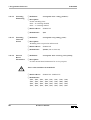
WARNING !
This equipment generates and can radiate radio frequencies. If not installed in accordance with the instruction manual, it may
cause interference to radio communications. The equipment has not been tested for compliance with the limits for class A
computing devices, pursuant to subpart J of part 15 of FCC rules, which are designed to provide reasonable protection against
such interference, but temporary usage is permitted as per regulations. Operation of this equipment in a residential area is
likely to cause interference, in which case the user, at his own expense is required to take whatever measures may be required
to shield the interference.
DISCLAIMER!
The information in this document has been carefully checked and is believed to be entirely reliable. However, no responsibility
is assumed for inaccuracies. ELTEC reserves the right to make changes to any products to improve reliability, function or
design. ELTEC does not assume any liability arising out of the application or use of any product or circuit described in this
manual; neither does it convey any license under its patent rights nor the rights of others. ELTEC products are not authorized
for use as components in life support devices or systems intended for surgical implant into the body or intended to support or
sustain life. Buyer agrees to notify ELTEC of any such intended end use whereupon ELTEC shall determine availability and
suitability of its product or products for the use intended.
ELTEC points out that there is no legal obligation to document internal relationships between any functional modules, realized
in either hardware or software, of a delivered entity.
This document contains copyrighted information. All rights including those of translation, reprint, broadcasting,
photomechanical or similar reproduction and storage or processing in computer systems, in whole or in part, are reserved.
EUROCOM is a trademark of ELTEC Elektronik AG. Other brands and their products are trademarks of their respective
holders and should be noted as such.
© 1995 ELTEC Elektronik AG, Mainz
ELTEC Elektronik AG
Galileo-Galilei-Str. 11
D-55129 Mainz
Telephone
Telefax
Postfach 42 13 63
D-55071 Mainz
+49 (61 31) 9 18-0
+49 (61 31) 9 18-1 99
BAB-40/60
Table of Contents
Table of Contents
Page
Table of Contents . . . . . . . . . . . . . . . . . . . . . . . . . . . . . . . . . . . . . . . . . . . . . . . . . . . . . . . . . . . . . . . . I
List of Tables . . . . . . . . . . . . . . . . . . . . . . . . . . . . . . . . . . . . . . . . . . . . . . . . . . . . . . . . . . . . . . . . . VII
List of Figures. . . . . . . . . . . . . . . . . . . . . . . . . . . . . . . . . . . . . . . . . . . . . . . . . . . . . . . . . . . . . . . . . . IX
Scope of Delivery . . . . . . . . . . . . . . . . . . . . . . . . . . . . . . . . . . . . . . . . . . . . . . . . . . . . . . . . . . . . . . . XI
Options . . . . . . . . . . . . . . . . . . . . . . . . . . . . . . . . . . . . . . . . . . . . . . . . . . . . . . . . . . . . . . . . . . . . . . . XI
Related Products . . . . . . . . . . . . . . . . . . . . . . . . . . . . . . . . . . . . . . . . . . . . . . . . . . . . . . . . . . . . . . . XII
Conventions . . . . . . . . . . . . . . . . . . . . . . . . . . . . . . . . . . . . . . . . . . . . . . . . . . . . . . . . . . . . . . . . . .XIII
How to Use this Manual . . . . . . . . . . . . . . . . . . . . . . . . . . . . . . . . . . . . . . . . . . . . . . . . . . . . . . . . . XV
1 Specification . . . . . . . . . . . . . . . . . . . . . . . . . . . . . . . . . . . . . . . . . . . . . . . . . . . . . . . . . . . . . . . . . . . 1
1.1
Main Features . . . . . . . . . . . . . . . . . . . . . . . . . . . . . . . . . . . . . . . . . . . . . . . . . . . . . . . . . . . . . . 1
1.2
General Description . . . . . . . . . . . . . . . . . . . . . . . . . . . . . . . . . . . . . . . . . . . . . . . . . . . . . . . . . . 2
1.3
Technical Details . . . . . . . . . . . . . . . . . . . . . . . . . . . . . . . . . . . . . . . . . . . . . . . . . . . . . . . . . . . . 5
1.3.1
CPU . . . . . . . . . . . . . . . . . . . . . . . . . . . . . . . . . . . . . . . . . . . . . . . . . . . . . . . . . . . . . . . 6
1.3.2
RAM Module . . . . . . . . . . . . . . . . . . . . . . . . . . . . . . . . . . . . . . . . . . . . . . . . . . . . . . . 7
1.3.3
PCMCIA Interface . . . . . . . . . . . . . . . . . . . . . . . . . . . . . . . . . . . . . . . . . . . . . . . . . . . 8
1.3.4
EPROM. . . . . . . . . . . . . . . . . . . . . . . . . . . . . . . . . . . . . . . . . . . . . . . . . . . . . . . . . . . . 8
1.3.5
Graphics/ Keyboard Interface (Optional) . . . . . . . . . . . . . . . . . . . . . . . . . . . . . . . . . . 8
1.3.6
Ethernet Interface . . . . . . . . . . . . . . . . . . . . . . . . . . . . . . . . . . . . . . . . . . . . . . . . . . . . 8
1.3.7
SCSI Interface . . . . . . . . . . . . . . . . . . . . . . . . . . . . . . . . . . . . . . . . . . . . . . . . . . . . . . . 9
1.3.8
Serial I/O . . . . . . . . . . . . . . . . . . . . . . . . . . . . . . . . . . . . . . . . . . . . . . . . . . . . . . . . . . . 9
1.3.9
CIO Counters/ Timers . . . . . . . . . . . . . . . . . . . . . . . . . . . . . . . . . . . . . . . . . . . . . . . . . 9
1.3.10
Parameter RAM and Real-Time Clock . . . . . . . . . . . . . . . . . . . . . . . . . . . . . . . . . . . . 9
1.3.11
Revision EEPROM . . . . . . . . . . . . . . . . . . . . . . . . . . . . . . . . . . . . . . . . . . . . . . . . . . . 9
1.3.12
VIC Timer . . . . . . . . . . . . . . . . . . . . . . . . . . . . . . . . . . . . . . . . . . . . . . . . . . . . . . . . . 10
1.3.13
Watchdog Timer . . . . . . . . . . . . . . . . . . . . . . . . . . . . . . . . . . . . . . . . . . . . . . . . . . . . 10
1.3.14
Status Display . . . . . . . . . . . . . . . . . . . . . . . . . . . . . . . . . . . . . . . . . . . . . . . . . . . . . . 10
Hardware Manual
I
Table of Contents (Continued)
BAB-40/60
Page
1.4
1.3.15
Reset . . . . . . . . . . . . . . . . . . . . . . . . . . . . . . . . . . . . . . . . . . . . . . . . . . . . . . . . . . . . . 10
1.3.16
VMEbus Interface . . . . . . . . . . . . . . . . . . . . . . . . . . . . . . . . . . . . . . . . . . . . . . . . . . . 11
1.3.16.1 System Controller . . . . . . . . . . . . . . . . . . . . . . . . . . . . . . . . . . . . . . . . . . . . 11
1.3.16.2 VMEbus Master Interface. . . . . . . . . . . . . . . . . . . . . . . . . . . . . . . . . . . . . . 11
1.3.16.3 VMEbus Slave Interface . . . . . . . . . . . . . . . . . . . . . . . . . . . . . . . . . . . . . . . 11
1.3.17
Interrupt Sources . . . . . . . . . . . . . . . . . . . . . . . . . . . . . . . . . . . . . . . . . . . . . . . . . . . . 11
1.3.18
BAB Extension Bus (BEB) . . . . . . . . . . . . . . . . . . . . . . . . . . . . . . . . . . . . . . . . . . . . 11
1.3.19
Software. . . . . . . . . . . . . . . . . . . . . . . . . . . . . . . . . . . . . . . . . . . . . . . . . . . . . . . . . . . 12
1.3.20
Connectors. . . . . . . . . . . . . . . . . . . . . . . . . . . . . . . . . . . . . . . . . . . . . . . . . . . . . . . . . 14
Definition of Board Parameters . . . . . . . . . . . . . . . . . . . . . . . . . . . . . . . . . . . . . . . . . . . . . . . . 21
1.4.1
VMEbus. . . . . . . . . . . . . . . . . . . . . . . . . . . . . . . . . . . . . . . . . . . . . . . . . . . . . . . . . . . 21
1.4.2
PCMCIA . . . . . . . . . . . . . . . . . . . . . . . . . . . . . . . . . . . . . . . . . . . . . . . . . . . . . . . . . . 22
1.4.3
Ethernet . . . . . . . . . . . . . . . . . . . . . . . . . . . . . . . . . . . . . . . . . . . . . . . . . . . . . . . . . . . 22
1.4.4
SCSI. . . . . . . . . . . . . . . . . . . . . . . . . . . . . . . . . . . . . . . . . . . . . . . . . . . . . . . . . . . . . . 22
1.4.5
Serial I/O . . . . . . . . . . . . . . . . . . . . . . . . . . . . . . . . . . . . . . . . . . . . . . . . . . . . . . . . . . 22
1.4.6
MTBF Values . . . . . . . . . . . . . . . . . . . . . . . . . . . . . . . . . . . . . . . . . . . . . . . . . . . . . . 22
1.4.7
Environmental Conditions. . . . . . . . . . . . . . . . . . . . . . . . . . . . . . . . . . . . . . . . . . . . . 23
1.4.8
Power Requirements . . . . . . . . . . . . . . . . . . . . . . . . . . . . . . . . . . . . . . . . . . . . . . . . . 23
2 Installation . . . . . . . . . . . . . . . . . . . . . . . . . . . . . . . . . . . . . . . . . . . . . . . . . . . . . . . . . . . . . . . . . . . 25
2.1
2.2
II
Introduction . . . . . . . . . . . . . . . . . . . . . . . . . . . . . . . . . . . . . . . . . . . . . . . . . . . . . . . . . . . . . . . 25
2.1.1
SIMM Installation . . . . . . . . . . . . . . . . . . . . . . . . . . . . . . . . . . . . . . . . . . . . . . . . . . . 25
2.1.2
PCMCIA Installation. . . . . . . . . . . . . . . . . . . . . . . . . . . . . . . . . . . . . . . . . . . . . . . . . 27
2.1.3
Board Installation . . . . . . . . . . . . . . . . . . . . . . . . . . . . . . . . . . . . . . . . . . . . . . . . . . . 28
2.1.3.1 Serial . . . . . . . . . . . . . . . . . . . . . . . . . . . . . . . . . . . . . . . . . . . . . . . . . . . . . . 28
2.1.3.2 Graphic . . . . . . . . . . . . . . . . . . . . . . . . . . . . . . . . . . . . . . . . . . . . . . . . . . . . 28
2.1.4
Serial Interface Level Converter (SILC) . . . . . . . . . . . . . . . . . . . . . . . . . . . . . . . . . . 28
2.1.5
Ethernet Installation . . . . . . . . . . . . . . . . . . . . . . . . . . . . . . . . . . . . . . . . . . . . . . . . . 29
2.1.6
SCSI Installation . . . . . . . . . . . . . . . . . . . . . . . . . . . . . . . . . . . . . . . . . . . . . . . . . . . . 29
Default Board Setting . . . . . . . . . . . . . . . . . . . . . . . . . . . . . . . . . . . . . . . . . . . . . . . . . . . . . . . 31
Hardware Manual
BAB-40/60
Table of Contents (Continued)
Page
2.3
Jumpers and Switches . . . . . . . . . . . . . . . . . . . . . . . . . . . . . . . . . . . . . . . . . . . . . . . . . . . . . . . 33
2.3.1
System Controller (J301) . . . . . . . . . . . . . . . . . . . . . . . . . . . . . . . . . . . . . . . . . . . . . 33
2.3.2
Serial Interface CHAN.2 Configuration . . . . . . . . . . . . . . . . . . . . . . . . . . . . . . . . . . 33
2.3.3
Reset (J1401). . . . . . . . . . . . . . . . . . . . . . . . . . . . . . . . . . . . . . . . . . . . . . . . . . . . . . . 35
2.3.4
Pin 1 Connection of EPROM (J1605). . . . . . . . . . . . . . . . . . . . . . . . . . . . . . . . . . . . 35
2.3.5
EEPROM Write Enable (J1702) . . . . . . . . . . . . . . . . . . . . . . . . . . . . . . . . . . . . . . . . 35
2.3.6
Switches . . . . . . . . . . . . . . . . . . . . . . . . . . . . . . . . . . . . . . . . . . . . . . . . . . . . . . . . . . 35
2.3.6.1 VMEbus Slave Address (S901) . . . . . . . . . . . . . . . . . . . . . . . . . . . . . . . . . 35
2.3.6.2 Hardware Configuration (S902) . . . . . . . . . . . . . . . . . . . . . . . . . . . . . . . . . 36
3 Programmers Reference . . . . . . . . . . . . . . . . . . . . . . . . . . . . . . . . . . . . . . . . . . . . . . . . . . . . . . . . 37
3.1
Address Map . . . . . . . . . . . . . . . . . . . . . . . . . . . . . . . . . . . . . . . . . . . . . . . . . . . . . . . . . . . . . . 37
3.2
DRAM . . . . . . . . . . . . . . . . . . . . . . . . . . . . . . . . . . . . . . . . . . . . . . . . . . . . . . . . . . . . . . . . . . . 39
3.3
3.4
3.2.1
RAM Access from the Local CPU . . . . . . . . . . . . . . . . . . . . . . . . . . . . . . . . . . . . . . 39
3.2.2
RAM Access from the VMEbus . . . . . . . . . . . . . . . . . . . . . . . . . . . . . . . . . . . . . . . . 39
3.2.3
Address Translation . . . . . . . . . . . . . . . . . . . . . . . . . . . . . . . . . . . . . . . . . . . . . . . . . 40
3.2.4
RAM Mirror . . . . . . . . . . . . . . . . . . . . . . . . . . . . . . . . . . . . . . . . . . . . . . . . . . . . . . . 41
3.2.5
RAM Access from the BEB . . . . . . . . . . . . . . . . . . . . . . . . . . . . . . . . . . . . . . . . . . . 41
3.2.6
RAM Access from ILACC . . . . . . . . . . . . . . . . . . . . . . . . . . . . . . . . . . . . . . . . . . . . 41
VMEbus Interface . . . . . . . . . . . . . . . . . . . . . . . . . . . . . . . . . . . . . . . . . . . . . . . . . . . . . . . . . . 42
3.3.1
System Controller . . . . . . . . . . . . . . . . . . . . . . . . . . . . . . . . . . . . . . . . . . . . . . . . . . . 42
3.3.2
VMEbus Master Interface . . . . . . . . . . . . . . . . . . . . . . . . . . . . . . . . . . . . . . . . . . . . .
3.3.2.1 Longword Access to Wordwide Slaves . . . . . . . . . . . . . . . . . . . . . . . . . . .
3.3.2.2 Address Modifier Source . . . . . . . . . . . . . . . . . . . . . . . . . . . . . . . . . . . . . .
3.3.2.3 Read-Modify-Write Cycles . . . . . . . . . . . . . . . . . . . . . . . . . . . . . . . . . . . .
3.3.2.4 A16 Slave Interface (ICMS). . . . . . . . . . . . . . . . . . . . . . . . . . . . . . . . . . . .
43
43
43
43
44
PCMCIA Interface. . . . . . . . . . . . . . . . . . . . . . . . . . . . . . . . . . . . . . . . . . . . . . . . . . . . . . . . . . 45
3.4.1
Interface Description . . . . . . . . . . . . . . . . . . . . . . . . . . . . . . . . . . . . . . . . . . . . . . . . . 45
3.4.2
Address Range . . . . . . . . . . . . . . . . . . . . . . . . . . . . . . . . . . . . . . . . . . . . . . . . . . . . . 45
3.4.3
Card Control Register (CCR) . . . . . . . . . . . . . . . . . . . . . . . . . . . . . . . . . . . . . . . . . . 46
3.4.4
Card Status Register (CSR). . . . . . . . . . . . . . . . . . . . . . . . . . . . . . . . . . . . . . . . . . . . 48
Hardware Manual
III
Table of Contents (Continued)
BAB-40/60
Page
3.4.5
Interrupt Vector Register (IVR) . . . . . . . . . . . . . . . . . . . . . . . . . . . . . . . . . . . . . . . . 49
3.4.6
Window Register (WIR) . . . . . . . . . . . . . . . . . . . . . . . . . . . . . . . . . . . . . . . . . . . . . . 50
3.5
VIC Timer . . . . . . . . . . . . . . . . . . . . . . . . . . . . . . . . . . . . . . . . . . . . . . . . . . . . . . . . . . . . . . . . 50
3.6
Battery-Backed Parameter RAM and Real-Time Clock . . . . . . . . . . . . . . . . . . . . . . . . . . . . . 51
3.6.1
Parameter RAM (NVRAM) . . . . . . . . . . . . . . . . . . . . . . . . . . . . . . . . . . . . . . . . . . . 51
3.6.2
Real-Time Clock . . . . . . . . . . . . . . . . . . . . . . . . . . . . . . . . . . . . . . . . . . . . . . . . . . . . 52
3.7
CIO Counter / Timer . . . . . . . . . . . . . . . . . . . . . . . . . . . . . . . . . . . . . . . . . . . . . . . . . . . . . . . . 53
3.8
Watchdog Timer . . . . . . . . . . . . . . . . . . . . . . . . . . . . . . . . . . . . . . . . . . . . . . . . . . . . . . . . . . . 54
3.9
Revision Information . . . . . . . . . . . . . . . . . . . . . . . . . . . . . . . . . . . . . . . . . . . . . . . . . . . . . . . . 56
3.10 Cache Coherency and Snooping . . . . . . . . . . . . . . . . . . . . . . . . . . . . . . . . . . . . . . . . . . . . . . . 58
3.11 Serial I/O . . . . . . . . . . . . . . . . . . . . . . . . . . . . . . . . . . . . . . . . . . . . . . . . . . . . . . . . . . . . . . . . . 59
3.11.1
Serial Communication Controller (SCC) . . . . . . . . . . . . . . . . . . . . . . . . . . . . . . . . . 59
3.11.2
Serial Interface Level Converter (SILC) . . . . . . . . . . . . . . . . . . . . . . . . . . . . . . . . . . 61
3.11.2.1 SILC Installation. . . . . . . . . . . . . . . . . . . . . . . . . . . . . . . . . . . . . . . . . . . . . 62
3.12 Ethernet Interface (802.3/10base5) . . . . . . . . . . . . . . . . . . . . . . . . . . . . . . . . . . . . . . . . . . . . . 63
3.13 SCSI Interface . . . . . . . . . . . . . . . . . . . . . . . . . . . . . . . . . . . . . . . . . . . . . . . . . . . . . . . . . . . . . 64
3.13.1
SCSI Controller . . . . . . . . . . . . . . . . . . . . . . . . . . . . . . . . . . . . . . . . . . . . . . . . . . . . . 64
3.14 IOC-2 . . . . . . . . . . . . . . . . . . . . . . . . . . . . . . . . . . . . . . . . . . . . . . . . . . . . . . . . . . . . . . . . . . . . 65
3.14.1
Register Set . . . . . . . . . . . . . . . . . . . . . . . . . . . . . . . . . . . . . . . . . . . . . . . . . . . . . . . . 65
3.15 Status Display . . . . . . . . . . . . . . . . . . . . . . . . . . . . . . . . . . . . . . . . . . . . . . . . . . . . . . . . . . . . . 67
3.16 Reset. . . . . . . . . . . . . . . . . . . . . . . . . . . . . . . . . . . . . . . . . . . . . . . . . . . . . . . . . . . . . . . . . . . . . 68
3.17 Bus Time-Out . . . . . . . . . . . . . . . . . . . . . . . . . . . . . . . . . . . . . . . . . . . . . . . . . . . . . . . . . . . . . 69
3.18 System Control Register (SCR). . . . . . . . . . . . . . . . . . . . . . . . . . . . . . . . . . . . . . . . . . . . . . . . 70
3.19 Interrupt Sources . . . . . . . . . . . . . . . . . . . . . . . . . . . . . . . . . . . . . . . . . . . . . . . . . . . . . . . . . . . 71
IV
3.19.1
Local Interrupt Sources . . . . . . . . . . . . . . . . . . . . . . . . . . . . . . . . . . . . . . . . . . . . . . . 73
3.19.2
VMEbus Interrupt Sources . . . . . . . . . . . . . . . . . . . . . . . . . . . . . . . . . . . . . . . . . . . . 73
Hardware Manual
BAB-40/60
Table of Contents (Continued)
Page
3.20 Indivisible Cycle Operation. . . . . . . . . . . . . . . . . . . . . . . . . . . . . . . . . . . . . . . . . . . . . . . . . . . 74
3.20.1
Deadlock Resolution . . . . . . . . . . . . . . . . . . . . . . . . . . . . . . . . . . . . . . . . . . . . . . . . . 74
3.20.2
TAS Violation on ‘040 . . . . . . . . . . . . . . . . . . . . . . . . . . . . . . . . . . . . . . . . . . . . . . . 74
3.21 Default Parameters for RMon . . . . . . . . . . . . . . . . . . . . . . . . . . . . . . . . . . . . . . . . . . . . . . . . . 75
3.21.1
Group A: I/O Initialization ($0000.0800 - $0000.0AEF) . . . . . . . . . . . . . . . . . . . . .
3.21.1.1 VIC Parameter . . . . . . . . . . . . . . . . . . . . . . . . . . . . . . . . . . . . . . . . . . . . .
3.21.1.2 SCC Port A Parameter. . . . . . . . . . . . . . . . . . . . . . . . . . . . . . . . . . . . . . .
3.21.1.3 SCC Port B Parameter . . . . . . . . . . . . . . . . . . . . . . . . . . . . . . . . . . . . . . .
3.21.1.4 CIO Parameter . . . . . . . . . . . . . . . . . . . . . . . . . . . . . . . . . . . . . . . . . . . . .
78
78
79
79
79
3.21.2
Group B: Address Information ($0000.0AF0 - $0000.0B47). . . . . . . . . . . . . . . . . .
3.21.2.1 ICF1 Address. . . . . . . . . . . . . . . . . . . . . . . . . . . . . . . . . . . . . . . . . . . . . .
3.21.2.2 VMEbus A32 Slave Address . . . . . . . . . . . . . . . . . . . . . . . . . . . . . . . . . .
3.21.2.3 VMEbus A32 Slave Size . . . . . . . . . . . . . . . . . . . . . . . . . . . . . . . . . . . . .
3.21.2.4 VMEbus Enable Bits . . . . . . . . . . . . . . . . . . . . . . . . . . . . . . . . . . . . . . . .
80
80
80
81
81
3.21.3
Group C: Hooks ($0000.0B48 - $0000.0B6F) . . . . . . . . . . . . . . . . . . . . . . . . . . . . . 81
3.21.4
Group D: Boot Parameters ($0000.0B70 - $0000.0C57) . . . . . . . . . . . . . . . . . . . . .
3.21.4.1 Autoboot Flag . . . . . . . . . . . . . . . . . . . . . . . . . . . . . . . . . . . . . . . . . . . . .
3.21.4.2 Operating System . . . . . . . . . . . . . . . . . . . . . . . . . . . . . . . . . . . . . . . . . .
3.21.4.3 SCSI Controller ID . . . . . . . . . . . . . . . . . . . . . . . . . . . . . . . . . . . . . . . . .
3.21.4.4 SCSI Controller Hardware . . . . . . . . . . . . . . . . . . . . . . . . . . . . . . . . . . .
3.21.4.5 SCSI Logical Unit Number . . . . . . . . . . . . . . . . . . . . . . . . . . . . . . . . . . .
3.21.4.6 Special Boot Flag . . . . . . . . . . . . . . . . . . . . . . . . . . . . . . . . . . . . . . . . . .
3.21.4.7 Sector Size . . . . . . . . . . . . . . . . . . . . . . . . . . . . . . . . . . . . . . . . . . . . . . . .
3.21.4.8 Base Address of RAM/ROM/ PCMCIA Boot . . . . . . . . . . . . . . . . . . . .
3.21.4.9 Retry Counter for Network Boot . . . . . . . . . . . . . . . . . . . . . . . . . . . . . . .
3.21.4.10 Delay until Auto Starts . . . . . . . . . . . . . . . . . . . . . . . . . . . . . . . . . . . . . .
3.21.4.11 Logical Sector Offset. . . . . . . . . . . . . . . . . . . . . . . . . . . . . . . . . . . . . . . .
3.21.4.12 Device Command . . . . . . . . . . . . . . . . . . . . . . . . . . . . . . . . . . . . . . . . . .
3.21.4.13 Own Internet Address . . . . . . . . . . . . . . . . . . . . . . . . . . . . . . . . . . . . . . .
3.21.4.14 Internet Boot File Name . . . . . . . . . . . . . . . . . . . . . . . . . . . . . . . . . . . . .
3.21.4.15 BootP Flag . . . . . . . . . . . . . . . . . . . . . . . . . . . . . . . . . . . . . . . . . . . . . . . .
3.21.4.16 Network Boot Time-out . . . . . . . . . . . . . . . . . . . . . . . . . . . . . . . . . . . . .
3.21.4.17 Server Name . . . . . . . . . . . . . . . . . . . . . . . . . . . . . . . . . . . . . . . . . . . . . .
82
82
82
82
83
83
83
84
84
84
84
85
85
85
86
86
86
87
3.21.5
Group E: Board Information ($0000.0C58 - $0000.0C9B) . . . . . . . . . . . . . . . . . . .
3.21.5.1 Character I/O Ports . . . . . . . . . . . . . . . . . . . . . . . . . . . . . . . . . . . . . . . . .
3.21.5.2 Watchdog Enable Flag . . . . . . . . . . . . . . . . . . . . . . . . . . . . . . . . . . . . . .
3.21.5.3 Watchdog Time-Out Period . . . . . . . . . . . . . . . . . . . . . . . . . . . . . . . . . .
3.21.5.4 Internal Board Information . . . . . . . . . . . . . . . . . . . . . . . . . . . . . . . . . . .
87
87
88
88
88
Hardware Manual
V
Table of Contents (Continued)
BAB-40/60
Page
3.21.5.5
3.21.5.6
3.21.5.7
3.21.5.8
Ethernet Node Address . . . . . . . . . . . . . . . . . . . . . . . . . . . . . . . . . . . . . . 89
CPU Board Identification . . . . . . . . . . . . . . . . . . . . . . . . . . . . . . . . . . . . 89
RMon Base Address . . . . . . . . . . . . . . . . . . . . . . . . . . . . . . . . . . . . . . . . 89
Size of Local Memory . . . . . . . . . . . . . . . . . . . . . . . . . . . . . . . . . . . . . . . 90
3.21.6
Group F: Video Descriptor . . . . . . . . . . . . . . . . . . . . . . . . . . . . . . . . . . . . . . . . . . . . 90
3.21.6.1 Graphic Mode . . . . . . . . . . . . . . . . . . . . . . . . . . . . . . . . . . . . . . . . . . . . . 90
3.21.6.2 Graphic Bit Mode . . . . . . . . . . . . . . . . . . . . . . . . . . . . . . . . . . . . . . . . . . 90
3.21.6.3 Display Start Address . . . . . . . . . . . . . . . . . . . . . . . . . . . . . . . . . . . . . . . 91
3.21.6.4 Size of Graphic Plane . . . . . . . . . . . . . . . . . . . . . . . . . . . . . . . . . . . . . . . 91
3.21.6.5 Size of Display Window . . . . . . . . . . . . . . . . . . . . . . . . . . . . . . . . . . . . . 91
3.21.6.6 Number of Fore-/Background Color . . . . . . . . . . . . . . . . . . . . . . . . . . . . 91
3.21.6.7 Number of Columns and Lines . . . . . . . . . . . . . . . . . . . . . . . . . . . . . . . . 92
3.21.6.8 Video Descriptor Format . . . . . . . . . . . . . . . . . . . . . . . . . . . . . . . . . . . . . 92
3.21.6.9 Position of Character Window. . . . . . . . . . . . . . . . . . . . . . . . . . . . . . . . . 92
3.21.6.10 Video Timing Parameter . . . . . . . . . . . . . . . . . . . . . . . . . . . . . . . . . . . . . 93
3.21.6.11 Keyboard Typamatic Rate . . . . . . . . . . . . . . . . . . . . . . . . . . . . . . . . . . . . 94
3.21.6.12 Keyboard Language . . . . . . . . . . . . . . . . . . . . . . . . . . . . . . . . . . . . . . . . . 94
3.21.7
Checksum . . . . . . . . . . . . . . . . . . . . . . . . . . . . . . . . . . . . . . . . . . . . . . . . . . . . . . . . . 94
Appendix:
A.1 Mnemonics Chart . . . . . . . . . . . . . . . . . . . . . . . . . . . . . . . . . . . . . . . . . . . . . . . . . . . . . . . . . . 96
A.1.1
Addressing Capabilities. . . . . . . . . . . . . . . . . . . . . . . . . . . . . . . . . . . . . . . . . . . . . . . 96
A.1.2
Data Transfer Capabilities. . . . . . . . . . . . . . . . . . . . . . . . . . . . . . . . . . . . . . . . . . . . . 96
A.1.3
Glossary. . . . . . . . . . . . . . . . . . . . . . . . . . . . . . . . . . . . . . . . . . . . . . . . . . . . . . . . . . . 97
A.2 Address Modifiers on VMEbus . . . . . . . . . . . . . . . . . . . . . . . . . . . . . . . . . . . . . . . . . . . . . . . 98
A.3 Index . . . . . . . . . . . . . . . . . . . . . . . . . . . . . . . . . . . . . . . . . . . . . . . . . . . . . . . . . . . . . . . . . . . . 99
A.4 References . . . . . . . . . . . . . . . . . . . . . . . . . . . . . . . . . . . . . . . . . . . . . . . . . . . . . . . . . . . . . . . 101
Technical Action Request Form Sheet
Reader Comments Form Sheet
VI
Hardware Manual
BAB-40/60
List of Tables
List of Tables
Page
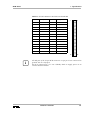
Table 1:
Table 2:
Table 3:
Table 4:
Table 5:
Table 6:
Table 7:
Table 8:
Table 9:
CAS2 Operations on the Various Busses . . . . . . . . . . . . . . . . . . . . . . . . . . . . . . . . . . . . . . . 6
Usable Bandwidth of the RAM . . . . . . . . . . . . . . . . . . . . . . . . . . . . . . . . . . . . . . . . . . . . . . . 7
6-Pin Telephone Jack Connector CHAN.1 (MOUSE/RS 232 PORT X701) . . . . . . . . . . . 14
15-Pin AUI Connector (ETHERNET X801) . . . . . . . . . . . . . . . . . . . . . . . . . . . . . . . . . . . 14
9-Pin Min-D Connector (male) CHAN.2 (X702) . . . . . . . . . . . . . . . . . . . . . . . . . . . . . . . . 15
Pin Assignment of VMEbus Connector (X101) . . . . . . . . . . . . . . . . . . . . . . . . . . . . . . . . . 16
Pin Assignment of Connector X102 . . . . . . . . . . . . . . . . . . . . . . . . . . . . . . . . . . . . . . . . . . 17
Pin Assignment of Power Connector (X103) . . . . . . . . . . . . . . . . . . . . . . . . . . . . . . . . . . . 18
Pin Assignment of BGB (X201) . . . . . . . . . . . . . . . . . . . . . . . . . . . . . . . . . . . . . . . . . . . . . 18
Table 10:
Table 11:
Table 12:
Table 13:
Table 14:
Table 15:
Table 16:
Table 17:
Table 18:
Table 19:
Pin Assignment of BEB (X222) . . . . . . . . . . . . . . . . . . . . . . . . . . . . . . . . . . . . . . . . . . . . .
SCSI Connector 8-bit X103 on ADAP-200 . . . . . . . . . . . . . . . . . . . . . . . . . . . . . . . . . . . .
Recommended SIMMs . . . . . . . . . . . . . . . . . . . . . . . . . . . . . . . . . . . . . . . . . . . . . . . . . . . .
Default Settings . . . . . . . . . . . . . . . . . . . . . . . . . . . . . . . . . . . . . . . . . . . . . . . . . . . . . . . . . .
J301 (System Controller). . . . . . . . . . . . . . . . . . . . . . . . . . . . . . . . . . . . . . . . . . . . . . . . . . .
J701 (CHAN.2 DCD/DSR Select) . . . . . . . . . . . . . . . . . . . . . . . . . . . . . . . . . . . . . . . . . . .
J702 (CHAN.2 DCD/Receive Clock Select). . . . . . . . . . . . . . . . . . . . . . . . . . . . . . . . . . . .
J703 (DTR/Transmit Clock Select) . . . . . . . . . . . . . . . . . . . . . . . . . . . . . . . . . . . . . . . . . . .
J1401 (Reset) . . . . . . . . . . . . . . . . . . . . . . . . . . . . . . . . . . . . . . . . . . . . . . . . . . . . . . . . . . . .
J1605 (Pin 1 Connection of EPROM). . . . . . . . . . . . . . . . . . . . . . . . . . . . . . . . . . . . . . . . .
19
20
26
31
33
33
34
34
35
35
Table 20:
Table 21:
Table 22:
Table 23:
Table 24:
Table 25:
Table 26:
Table 27:
Table 28:
Table 29:
J1702 (EEPROM Write Enable) . . . . . . . . . . . . . . . . . . . . . . . . . . . . . . . . . . . . . . . . . . . . .
Hex Switch S901 (VMEbus Slave Address) . . . . . . . . . . . . . . . . . . . . . . . . . . . . . . . . . . . .
Hex Switch S902 (Hardware Configuration) . . . . . . . . . . . . . . . . . . . . . . . . . . . . . . . . . . .
Address Assignment of BAB-40/60 . . . . . . . . . . . . . . . . . . . . . . . . . . . . . . . . . . . . . . . . . .
Local I/O Address Assignment for BAB-40/60 . . . . . . . . . . . . . . . . . . . . . . . . . . . . . . . . .
Slave Base Address Register Layout. . . . . . . . . . . . . . . . . . . . . . . . . . . . . . . . . . . . . . . . . .
Enable Slave Register Layout . . . . . . . . . . . . . . . . . . . . . . . . . . . . . . . . . . . . . . . . . . . . . . .
Intercommunication Register Location on VMEbus. . . . . . . . . . . . . . . . . . . . . . . . . . . . . .
Address Assignment of SRAM/RTC . . . . . . . . . . . . . . . . . . . . . . . . . . . . . . . . . . . . . . . . .
Address Assignment of the Real-Time Clock . . . . . . . . . . . . . . . . . . . . . . . . . . . . . . . . . . .
35
36
36
37
38
39
40
44
51
52
Table 30:
Table 31:
Table 32:
Table 33:
Table 34:
Address Assignment of the System CIO . . . . . . . . . . . . . . . . . . . . . . . . . . . . . . . . . . . . . . .
Address Assignment of Watchdog Registers . . . . . . . . . . . . . . . . . . . . . . . . . . . . . . . . . . .
Watchdog Configuration Register at $FEC5.2000 . . . . . . . . . . . . . . . . . . . . . . . . . . . . . . .
IOC-2 Control Register at $FEC7.00A8 . . . . . . . . . . . . . . . . . . . . . . . . . . . . . . . . . . . . . . .
I2C Control Register Layout . . . . . . . . . . . . . . . . . . . . . . . . . . . . . . . . . . . . . . . . . . . . . . . .
53
54
55
56
56
Hardware Manual
VII
List of Tables (Continued)
BAB-40/60
Page
Table 35:
Table 36:
Table 37:
Table 38:
Table 39:
Address Map of the Serial EEPROM . . . . . . . . . . . . . . . . . . . . . . . . . . . . . . . . . . . . . . . . . 57
Snoop Control Register Layout for BAB-40/60 . . . . . . . . . . . . . . . . . . . . . . . . . . . . . . . . . 58
Snoop Control Encoding for BAB-40 . . . . . . . . . . . . . . . . . . . . . . . . . . . . . . . . . . . . . . . . . 58
Snoop Control Encoding for BAB-60 . . . . . . . . . . . . . . . . . . . . . . . . . . . . . . . . . . . . . . . . . 58
RAM Size . . . . . . . . . . . . . . . . . . . . . . . . . . . . . . . . . . . . . . . . . . . . . . . . . . . . . . . . . . . . . . 58
Table 40:
Table 41:
Table 42:
Table 43:
Table 44:
Table 45:
Table 46:
Table 47:
Table 48:
Table 49:
Time Constant Values for SCC . . . . . . . . . . . . . . . . . . . . . . . . . . . . . . . . . . . . . . . . . . . . . . 59
Address Assignment of the SCC . . . . . . . . . . . . . . . . . . . . . . . . . . . . . . . . . . . . . . . . . . . . . 60
Pin Assignment for SILCs . . . . . . . . . . . . . . . . . . . . . . . . . . . . . . . . . . . . . . . . . . . . . . . . . . 62
Ethernet Controller Address Layout . . . . . . . . . . . . . . . . . . . . . . . . . . . . . . . . . . . . . . . . . . 63
Register Map . . . . . . . . . . . . . . . . . . . . . . . . . . . . . . . . . . . . . . . . . . . . . . . . . . . . . . . . . . . . 65
Reset Conditions . . . . . . . . . . . . . . . . . . . . . . . . . . . . . . . . . . . . . . . . . . . . . . . . . . . . . . . . . 68
System Control Register Layout (System CIO) . . . . . . . . . . . . . . . . . . . . . . . . . . . . . . . . . 70
VIC Interrupt Priority Scheme. . . . . . . . . . . . . . . . . . . . . . . . . . . . . . . . . . . . . . . . . . . . . . . 72
Local Interrupt Sources . . . . . . . . . . . . . . . . . . . . . . . . . . . . . . . . . . . . . . . . . . . . . . . . . . . . 73
Default Parameters of RMon 2.8 located on BAB-40/60 . . . . . . . . . . . . . . . . . . . . . . . . . . 75
VIII
Hardware Manual
BAB-40/60
List of Figures
List of Figures
Page
Figure 1:
Figure 2:
Figure 3:
Figure 4:
Figure 5:
Figure 6:
Figure 7:
Figure 8:
Figure 9:
Block Diagram . . . . . . . . . . . . . . . . . . . . . . . . . . . . . . . . . . . . . . . . . . . . . . . . . . . . . . . . . . . 2
PCMCIA Installation. . . . . . . . . . . . . . . . . . . . . . . . . . . . . . . . . . . . . . . . . . . . . . . . . . . . . . 27
Installation Diagram . . . . . . . . . . . . . . . . . . . . . . . . . . . . . . . . . . . . . . . . . . . . . . . . . . . . . . 30
Location of Jumpers, Interface Connectors and Switches . . . . . . . . . . . . . . . . . . . . . . . . . 32
Serial Interface CHAN.2 Configuration . . . . . . . . . . . . . . . . . . . . . . . . . . . . . . . . . . . . . . . 34
Relative Address Space . . . . . . . . . . . . . . . . . . . . . . . . . . . . . . . . . . . . . . . . . . . . . . . . . . . . 45
PCMCIA Interface Configuration Registers . . . . . . . . . . . . . . . . . . . . . . . . . . . . . . . . . . . . 46
Card Control Register (CCR) . . . . . . . . . . . . . . . . . . . . . . . . . . . . . . . . . . . . . . . . . . . . . . . 46
Timing . . . . . . . . . . . . . . . . . . . . . . . . . . . . . . . . . . . . . . . . . . . . . . . . . . . . . . . . . . . . . . . . . 47
Figure 10: Card Status Register (CSR). . . . . . . . . . . . . . . . . . . . . . . . . . . . . . . . . . . . . . . . . . . . . . . . . 48
Figure 11: Interrupt Vector Register (IVR) . . . . . . . . . . . . . . . . . . . . . . . . . . . . . . . . . . . . . . . . . . . . . 49
Figure 12: Window Register (WIR) . . . . . . . . . . . . . . . . . . . . . . . . . . . . . . . . . . . . . . . . . . . . . . . . . . . 50
Hardware Manual
IX
BAB-40/60
X
Hardware Manual
BAB-40/60
Scope of Delivery / Options
Scope of Delivery
Description:
Order No.:
BAB-40
Basic Automation Board
V-BAB.-A400
BAB-60
Basic Automation Board
V-BAB.-A600
Options
Description:
Order No.:
SCSI
V-BAB.-Z001
SCSI option
i
The last letter of the order numbers refers to the hardware revision and is
subject to changes. Please contact ELTEC for information about valid
order numbers.
Example:
V-E16.-B105
Revision number, subject to change!
Hardware Manual
XI
Related Products
BAB-40/60
Related Products
Description:
Order No.:
Documentation:
Hardware:
i
Hardware Manual BAB-40/60
V-BAB.-A490
Service Manual BAB-40/60 including:
Software Manual RMon (W-FIRM-A209)
BEB Specification (V-BEB.-A990)
IOC-2 Data Sheet (V-DTBT-A924)
Z85230 (V-DTBT-A935)
MK48T02/12 (V-DTBT-A907)
Z8536 (V-DTBT-A908)
VIC068 (V-DTBT-B914)
NCR53C710 (V-DTBT-A934)
ILACC AM79C900 (V-DTBT-A925)
V-BAB.-A491
BAB Graphics Module
V-BAB.-A410
ADAP: to adapt signals on P2 to
SCSI (8-bit) and I/O signals
V-ADAP-A200
ADAP: to connect AT-keyboard to
PS/2 compatible connector
V-ADAP-A210
CONV: Cheapernet/10BaseT MAU
V-CONV-A500
RS 232 SILC
V-SILC-E200
RS 422 SILC
V-SILC-B300
RS 485 SILC
V-SILC-A400
Cable (V.24 for terminal)
V-CABL-A144
The last letter of the order numbers refers to the hardware revision and is
subject to changes. Please contact ELTEC for information about valid
order numbers.
Example:
V-E16.-B105
Revision number, subject to change!
XII
Hardware Manual
BAB-40/60
Conventions
Conventions
If not otherwise specified, addresses are written in hexadecimal notation
and identified by a leading dollar sign ("$").
Signal names preceded by a slash ("/"), indicate that this signal is either
active low or that this signal becomes active with the trailing edge.
b
B
K
M
MHz
bit
byte
kilo, means the factor 400 in hex (1024 decimal)
mega, the multiplication with 100 000 in hex (1 048576 decimal)
1 000 000 Hertz
Board-specific abbreviations:
ASR
AUI
BEB
BGB
BLT
BTO
CAS
CAS2
CLUT
CPU
CSR
CTS
DAC
DMA
DTE
EEPROM
EPROM
ESR
FIFO
FPU
IACK
ICF
ICGS
ICMS
ILACC
IOC-2
Address Substitution Register
Attachment Unit Interface
BAB Extension Bus
BAB Graphic Bus
Block Transfer
Bus Time-out
Column Address Strobe
Compare and Swap 2 Instruction
Color Look-up Table
Central Processing Unit
Control/Status Register
Clear to Send
Digital to Analog Converter
Direct Memory Access
Data Terminal Equipment
Electrically Erasable Programmable Read Only Memory
Erasable Programmable Read Only Memory
Enable Slave Register
First In First Out
Floating Point Unit
Interrupt Acknowledge
Interprocessor Communication Facility
Interprocessor Communication Global Switches
Interprocessor Communication Module Switches
Integrated Local Area Communications Controller
I/O Controller Asic
Hardware Manual
XIII
Conventions (Continued)
BAB-40/60
LAN
LIRQ
MAU
MBAR
MMU
NVRAM
PCB
PCMCIA
PLD
PLL
RAM
RAS
RMC
RTC
RTS
SBR
SCSI
SCR
SILC
SRAM
SMR
TTL
VIC
VRAM
UAT
XIV
Local Area Network
Local Interrupt Request
Medium Attachment Unit
Memory Base Address Register
Memory Management Unit
Nonvolatile RAM
Printed Circuit Board
Personal Computer Memory Card International Association
Programmable Logic Device
Phase Locked Loop
Random Access Memory
Row Address Strobe
Read-Modify-Write Cycle
Real-time Clock
Request to Send
Slave Base Address Register
Small Computer Systems Interface
System Control Register
Serial Interface Level Converter
Static RAM
Slave Mask Register
Transistor Transistor Logic
VMEbus Interface Chip
Video RAM
Unaligned Transfer
Hardware Manual
BAB-40/60
How to Use this Manual
How to Use this Manual
Document Structure
This manual is divided into the following chapters:
Chapter 1 Specification contains a list of distinguishing features, a block
diagram with a general description, a description of the main building
blocks and the board parameters.
Chapter 2 Installation describes the requirements and the step-by-step
installation. A table shows the default settings of jumpers and switches
followed by a detailed description of adjustable functions.
Chapter 3 Programmer Reference shows the address map and describes
the address ranges in detail. Special functions are also described in this
chapter.
The Appendix contains references to additional literature, an index, and a
glossary and necessary extracts of data sheets.
Document Conventions
Font Types:
Font
Use
Helvetica, 8 Pt
Tables and drawings
Helvetica, 10 Pt
Signal names, formulars
Times, italic
Notes
Courier, bold
Program code, function names,
commands
Times, bold
Emphasized text, e.g. headlines
Hardware Manual
XV
How to Use this Manual (Continued)
BAB-40/60
Other Conventions:
i
!
Indicates information that requires close attention.
Indicates critical information that is essential to read.
Indicates information that is imperative to read. Skipping this
material, possibly causes damage to the system.
XVI
Hardware Manual
BAB-40/60
1 Specification
1 Specification
1.1 Main Features
•One 68(EC)040/060 CPU at 50 MHz or 66 MHz
•Memory
- PS/2 SIMM memory module (1, 2, 8, 16, 32 MB) for data/program
storage (44 MB/s at 33 MHz bus speed)
- 2 KB SRAM and RTC for storage of variable system parameters
MK48T12 (MK48T18/8 KB, DS1644/32 KB)
- Up to 1 MB x 8 K EPROM
•Two PCMCIA sockets on front panel for two type I or II PC Cards or one
type III PC Card (Flash, SRAM and ATA-HD only)
•One internal PCMCIA socket (type I, type II, or with some restrictions
type III (Flash, SRAM and ATA-HD only))
•Ethernet interface (32-bit ILACC)
•VMEbus Interface Controller:
- System controller and arbiter
- VMEbus interrupter and interrupt handler
- 32-bit slave BLT 20 MB/s
- Master / slave write posting
•IOC-2 gate array:
- 68040 to 68020 bus converter
- Dynamic bus sizing for VMEbus and BEB
- Translation of BLT into bursts on '040 bus to allow snooping of BLT
cycles
- Separate arbitration on '040 and '020 bus
- I/O bus interface
- Support for VMEbus UATs to allow snooping
- Interface for a single bytewide EPROM
•Three 16-bit timer / counter
•Two serial ports (RS 232, RS 422, RS 485)
•Smart SCSI-2 (NCR 53C710) interface with burst capability (max.
transfer capacity 10 MB/s) and single-ended 8-bit SCSI data bus
•Two rotary switches for selection of operation modes and base address
•Status display on front panel
•Watchdog timer 130 ms ... 17 min
•BEB for interfacing to various mezzanine busses
•BGB for graphic and keyboard module
Hardware Manual
1
1 Specification
BAB-40/60
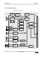
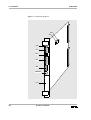
1.2 General Description
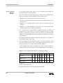
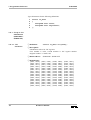
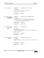
Figure 1: Block Diagram
CPU
68040/060
50/66 MHz
Memory
Module
1-32 MB
Front
Panel
NCR53C710
SCSI
Controller
8-bit SCSI-2
VMEbus
‘
040 Bus
CIO
8536
I/O Bus
IOC-2
Watchdog
1M x 8
EPROM
VMEbus
Controller
X101
Slave Operation
Addr.
Mode
32KB/2KB x 8
NVRAM
RTC
VMEbus
Buffer/Count./
Decoder
SILC
RS232
Serial
Controller
8530
Revision
EEPROM
512 x 8
Serial Line
Ethernet
Controller
ILACC
A
U
I
‘
020 Bus
Row A
Row C
Graphic
Module
Row B
512 KB / 1 MB
VRAM/
Video Contr.
Keyboard
Controller
X102
V
G
A
BGB
Keyboard
PCMCIA2
PCMCIA1
2
PCMCIA
Controller
PCMCIA0
BEB
Hardware Manual
BAB-40/60
1 Specification
The BAB-40/60 is a highly integrated high-performance single-board
VMEbus computer with optional graphics display. It is designed to offer
as many features as possible on a single slot VMEbus board. Suitable
intelligent or high integrated components are used to achieve this density
of computing power.
On the BAB-40 there is one 68040 CPU, clocked at 50 or 66 MHz. Onchip caches for program and data (4 KB capacity each) and the on-chip
floating-point units allow 35 MIPS at 66 MHz.
The 68060 CPU on the BAB-60 offers 2.5 times the performance of a
68040 clocked at the same frequency.
Additionally, backward compatibility with existing 68000-family
software is guaranteed.
The main memory is placed on a separate PS/2 SIMM memory module.
This easily allows to expand the memory up to 32 MB without any
changes necessary at the CPU board. The main memory is directly
accessed via the 32-bit processor bus.
The major drawback of the 68040/60 is the deletion of dynamic bus
sizing. This requires 68020/30 applications to be modified if they access
word devices with longword instructions. The longword accesses have to
be split by software into two word accesses which slows down the
performance. Instead of this, the IOC-2 hardware generates the needed
bus cycles if the addressed device acknowledges a smaller data size than
the CPU requested.
One of the main design goals of the BAB-40/60 is efficient use of the
CPU's high speed bus. Thus, the following design rules are established:
•Use of intelligent peripheral devices which are able to perform tasks
independent from the main CPU (NCR 53C710, ILACC).
•Independent 68020-like bus for VMEbus, Ethernet or BEB with separate
arbitration.
•Minimum interference between CPU bus, ‘020 bus and I/O bus.
•Decoupling of VMEbus and CPU bus via FIFO for BLT.
On traditional designs there could only be one bus master on the whole
board at a time. For example, if a BLT was in progress, the CPU was
blocked for the duration of the BLT. At the BAB-40/60 the FIFO in the
IOC-2 collects the data while the CPU still accesses the DRAM.
Hardware Manual
3
1 Specification
BAB-40/60
In order to enhance system security, the BAB-40/60 incorporates a
watchdog timer. It must be retriggered periodically, otherwise the
watchdog generates a reset.
Two serial ports are located on the BAB-40/60. One, using a 6-pin
shielded RJ11 jack on the front panel, is intended for connection of a
terminal or a mouse. The other uses a 9-pin Min-D male connector on the
front panel. It can be configured to support either RS 232 or RS 422/485
standard via SILCs (Serial Interface Level Converters).
The integrated real-time clock allows the operating system to provide date
and time for revision control. The clock is powered by an internal lithium
battery. 2 (8, 32) KB of battery-backed RAM are used for storage of
system dependent parameters.
The four LED status display on the front panel indicates the condition of
the processor.
Two hex-code switches (software readable) are used by the firmware to
set up the operating mode and the VMEbus base address of the board.
The VMEbus interface of the BAB-40/60 uses the VIC068 VMEbus
Interface Controller gate array.
One 1M x 8 EPROM holds the firmware.
The on-board Ethernet interface provides connection to most popular local
area networks (LAN).
A sophisticated SCSI-2 interface is also located on the BAB-40/60. The
controller chip is very fast and intelligent so that it forms a very efficient
SCSI interface with max. transfer rates of 10 MB/s.
The on-board BAB extension bus (BEB) allows easy hardware extension
of the BAB-40/60 using various mezzanine busses.
The BAB graphic bus (BGB) allows flexible extension of the BAB with
graphics/keyboard modules.
The three PCMCIA sockets support several types of PC Cards (harddisks,
SRAM, Flash EPROM, ...).
4
Hardware Manual
BAB-40/60
1 Specification
1.3 Technical Details
The BAB-40/60 consists of the following main blocks:
•CPU
•RAM Module
•PCMCIA Interface
•EPROM
•Graphics/Keyboard Interface (optional)
•Ethernet Interface
•SCSI Interface
•Serial I/0
•CIO Counters / Timers
•Parameter RAM and Real-Time Clock
•Revision EEPROM
•VIC Timer
•Watchdog Timer
•Status Display
•Reset
•VMEbus Interface
•Interrupt Sources
•BAB Extension Bus
•Software
•Connectors
Hardware Manual
5
1 Specification
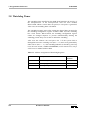
1.3.1
CPU
BAB-40/60
The BAB-40/60 is equipped with Motorola’s 68040/060 CPU, clocked
with 50 or 66 MHz. All internal bus operations are synchronous to this
clock. The CPU uses burst mode to access the main memory. The BAB-60
uses the 68040 bus mode of the 68060.
The CPU handles all interrupts generated by the VIC.
Non-interruptable read-modify-write cycles (TAS command) are
supported between VMEbus and the CPU. RMC cycles from the VMEbus
to the local RAM are only indivisible when they are byte size. CAS2
instructions have limited support.
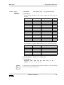
Table 1: CAS2 Operations on the Various Busses
6
1st op
2nd op
indivisible
local RAM
local RAM
yes
'020 bus (BEB)
local RAM
yes
VMEbus
local RAM
yes
local RAM
'020 bus (BEB)
no
'020 bus (BEB)
'020 bus (BEB)
yes
VMEbus
'020 bus (BEB)
yes
local RAM
VMEbus
no
'020 bus (BEB)
VMEbus
no
VMEbus
VMEbus
yes
Hardware Manual
BAB-40/60
1.3.2
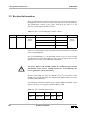
1 Specification
RAM Module
The DRAM is accessed by the following sources:
•CPU
•SCSI Controller
•Ethernet Controller
•BEB
•VMEbus
Burst mode is supported for accesses of:
•CPU
•SCSI Controller
•VMEbus BLT
The base address of the DRAM seen from the CPUs is fixed to
$0000.0000. To avoid programming of the MMU, the DRAM is mirrored
as non-cacheable RAM.
The base address for accessing the RAM from the VMEbus as well as the
window size is programmable. The on-board firmware uses hex switch
S901 to program the VMEbus address decoder and mask registers.
i
When using A24 addressing from the BEB, to access the BAB-40/60 RAM,
the address translation logic has to be programmed to supply the local
addresses A(24) to A(26).
The following table summarizes the usable bandwidth of the RAM
including precharge and refresh.
Table 2: Usable Bandwidth of the RAM
Bus Clock
33 MHz: (MB/s)
25 MHz: (MB/s)
DRAM read
44
40
DRAM write
44
40
Hardware Manual
7
1 Specification
BAB-40/60
1.3.3
PCMCIA
Interface
The three socket PCMCIA interface uses a MACH445 PLD. It
incorporates several control registers and translates the signals from the
BAB’s ‘020 bus to the three PCMCIA sockets. The data and address lines
of the sockets are isolated from the ‘020 bus via buffers. This allows live
insertion and removal of PC Cards under certain circumstances (when
none of the PC Cards is accessed by the CPU). To ensure that unused
areas of a PC Card are read as ‘1’the data lines of each slot are pulled
high. To allow programming of FLASH devices +12 V can be applied to
the sockets via optocoupler devices.
1.3.4
EPROM
The pin assignment of the 32-pin socket corresponds with the JEDEC
standard. The socket is designed for use with 32-pin EPROMs only. These
EPROM types range from 1 Mb up to 8 Mb (27C010 to 27C080).
The EPROM access time is programmable via IOC-2 register from 4 to 36
wait-states (60 ns to 810 ns maximum access time).
After reset, the EPROM is mapped to $0000.0000 so the initial stack
pointer and reset vector can be read. During initialization, it is mapped to
its normal address ($FE80.0000) and the DRAM is located at address
$0000.0000. The EPROM is accessed with six wait-states (120 ns access
time) per byte at 33 MHz.
The software in the basic EPROM (RMon) initializes all hardware
according to the parameters in the basic EPROM or the NVRAM
($FEC2.0000).
1.3.5
Graphics/
Keyboard
Interface
(Optional)
Various graphics/keyboard modules can be installed on the BAB-40/60
via the BGB connector. All modules support a PS/2 compatible keyboard.
The standard module has 1 MB VRAM and displays up to
1024x768 pixels with 4/8 bit per pixel and 60 MHz refresh rate. Up to
800x600 72 Hz refresh rate is possible. The monitor is connected to the
module via a standard 15-pin VGA connector.
1.3.6
Ethernet
Interface
The Ethernet interface is based on the Integrated Local Area
Communications Controller (ILACC - AM79C900).
A main feature of the ILACC and its on-chip DMA channel is the
flexibility and speed of communication. The internal Manchester
Encoder / Decoder of the ILACC is compatible with the IEEE-802.3
specification. Via the AUI connector on the front panel the BAB-40/60 is
attached to Ethernet (Cheapernet, 10BaseT) networks.
8
Hardware Manual
BAB-40/60
1.3.7
SCSI Interface
1 Specification
Single-ended 8-bit SCSI-2 signals are fed into row A and C of the
VMEbus P2 connector (X102). An ADAP-200 is plugged onto the rear
side of the backplane to interface to standard 8-bit SCSI connectors.
The NCR53C710 SCSI controller uses its own code fetching and SCSI
data transfer from the DRAM. The processor executes SCSI SCRIPTS to
control the actions on the SCSI and the CPU bus. SCRIPTS is a specially
designed language for easy SCSI protocol handling. It dramatically
reduces the CPU activities. The SCRIPTS processor starts SCSI I/O
operations in approximately 500 ns where traditional intelligent host
adapters require 2-8 ms.
1.3.8
Serial I/O
The BAB-40/60 offers two serial I/O lines, implemented by one Z8530
SCC. CHAN.1 is a RS 232 two wire handshake interface. CHAN.2 uses a
removable serial interface level converters (SILC). As shipped, a RS 232
level converter SILC is installed featuring hardware handshake as well as
the XON / XOFF protocol. Additional level converter plug-ins for RS 422
and RS 485 are available.
The baud rate generator is driven by 5 MHz, allowing baud rates from
50 b/s to 38.4 kb/s.
1.3.9
CIO Counters/
Timers
The BAB-40/60 offers three independent, programmable 16-bit
counters / timers integrated in the CIO.
1.3.10 Parameter
RAM and RealTime Clock
The real-time clock is designed with the MK48T12 timekeeper RAM. It
combines a 2KBx8 CMOS SRAM (parameter RAM, NVRAM), a
bytewide accessible real-time clock, a crystal, and a long-life lithium
battery, all in one package. Alternatively, a MK48T18 device can be used
which offers 8 KB SRAM or a DS1644 device which offers 32Kx8 KB
SRAM.
1.3.11 Revision
EEPROM
The revision EEPROM is realized by a 512x8B serial EEPROM which
offers special board revision information. The lower half size of the
EEPROM is programmed by ELTEC and should not be modified by the
user to guarantee board revision consistency. The upper 256 B can be used
by the user to store additional information.
Hardware Manual
9
1 Specification
BAB-40/60
1.3.12 VIC Timer
The VIC contains a timer which can be programmed to output a periodic
wave form on LIRQ2. The available frequencies are 50 Hz, 100 Hz, and
1000 Hz. The VIC timer is typically used as a tick timer for multi-tasking
operating systems.
1.3.13 Watchdog
Timer
The watchdog timer monitors the activity of the microprocessor. If the
microprocessor does not access the watchdog timer within the time-out
period of 130 ms to 17 min, a reset pulse is generated. After reset, the
watchdog timer is disabled. The time-out period becomes effective after
the first access to the watchdog configuration register.
After reset the software can read PA7 of the CIO to distinguish between a
watchdog reset and a reset generated by other sources. This watchdog
indicator is only cleared by power-up reset, the reset switch, a VMEbus
SYSRESET, a VIC remote reset, or by a write access to the watchdog.
The time-out period is derived from a quartz oscillator so that tolerances
can be neglected.
1.3.14 Status Display
The BAB-40/60 features a four LED display on the front panel and
displays values from 0 - F.
This status display ($FEC3.0000) is designed as a read / write register and
uses the least significant nibble of the byte.
1.3.15 Reset
Reset may be initiated by six sources:
•supply voltage drop below 4.75 V or power-up
•reset jumper J1401
•VMEbus SYSRESET
•VIC remote control reset register
•Watchdog
•CPU RESET instruction
10
Hardware Manual
BAB-40/60
1 Specification
1.3.16 VMEbus
Interface
Each BAB-40/60 board offers VMEbus master and slave interfaces.
Additionally, VMEbus system controller functions are available via the
VMEbus gate array (VIC).
1.3.16.1 System
Controller
The BAB-40/60 features a full slot-one system controller, including
SYSCLK , SYSRESET , bus time-out, IACK daisy chain driver, and a four
level arbitration circuit. System controller capabilities are enabled when
J301 is closed.
1.3.16.2 VMEbus
Master
Interface
The master interface of the BAB-40/60 board supports 8, 16, and 32-bit
data transfer cycles in A32, A24, and A16 addressing modes.
A special feature is provided to support longword accesses from the local
CPU to D16 VMEbus boards (dynamic bus sizing). Two control lines of
the SCR enable longword breaking for the A32 and A24 area.
The VIC chip supplies the VMEbus address modifier signals. This is done
by either routing FC0..2 line to AM0..2, or by driving these signals by an
internal address modifier source register of the VIC ($FEC0.10B7). The
AM3..5 lines are driven depending on the actual data size, or by the
address modifier source register. One output signal of the system control
register is used to control this option.
The BAB-40/60 supports slave block transfer cycles.
1.3.16.3 VMEbus Slave
Interface
The BAB-40/60 supports A32 slave access to the DRAM and an A16
slave interface to access the interprocessor communication registers. The
addresses for all of the slave interfaces are separately programmable.
1.3.17 Interrupt
Sources
The BAB-40/60 allows full utilization of both the powerful VMEbus
interrupt structure and the 68040/060 CPU design.
1.3.18 BAB Extension
Bus (BEB)
The BEB port of the BAB-40/60 can carry slave-only, master-only or
master-slave boards. The IRQ line of the BEB is connected to VIC’s
LIRQ5 input. The VIC has to be programmed to generate interrupts on
level 2, because only level 2 IACK cycles are routed to the BEB.
Hardware Manual
11
1 Specification
1.3.19 Software
BAB-40/60
The local BAB-40/60 firmware (RMon) is stored in the on-board
EPROM. RMon provides the basic software layer of the board. Any
operating system or application software is based on the RMon and uses
its functionality:
•Power-On Initialization
•Configuration
•Various Bootstraps
•Externally Callable I/O Functions
•Application Hooks
Power-On Initialization
After RESET or power-on, the local hardware (VIC, serial I/O, CIO,
video, keyboard interface, etc.) has to be initialized by the CPU. The
initialization is affected by certain parameters taken either from the onboard NVRAM or from the EPROM (default values). Hex switch S902
selects whether the NVRAM or the default values are to be used.
The NVRAM parameters are certified by a checksum. If the checksum test
fails, the default parameters are used independent of the switch setting.
After reset or power-on an automatic selftest routine checks the functional
groups of the board and displays its results.
Configuration
The configuration program is completely menu driven. The program
interactively shows the configuration parameters and allows their
modification:
•I/O Configuration, e.g.: serial I/O, AT-keyboard, on-board video, baud
rate, etc.
•Video Mode
•Bootstrap Configuration
•Internet Address of ILACC
•VMEbus Interface Configuration (VIC Programming)
12
Hardware Manual
BAB-40/60
1 Specification
Various Bootstraps
•OS-9 from SCSI Floppy
•OS-9 from SCSI Harddisk
•OS-9 from SCSI Tape
•OS-9 from ROM/RAM Disk
•OS-9 from PCMCIA
•Lynx from Tape
•Lynx from Harddisk
•Lynx from Floppy
•tftp-bootstrap from Ethernet including ARP and RARP protocols
•ROMed application bootstrap, suitable as well for VMEbus-downloaded
applications under control of a VMEbus host
External Callable I/O Functions
•Enable/Disable IRQs
•Get Device Status
•Set Device Mode
•Character Raw I/O
•C-like functions getchar, putchar, printf
Application Hooks
Application programs may freely use the externally callable I/O functions
and other information provided in the ‘RMon Fixed Public Location’.
Furthermore, a ROMed application can very easily be started interactively
or automatically after RESET or power-on from RMon. The application
autostart mechanism can be installed simply by setting the respective
bootstrap configuration parameters.
Hardware Manual
13
1 Specification
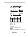
1.3.20 Connectors
BAB-40/60
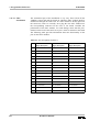
Table 3: 6-Pin Telephone Jack Connector CHAN.1
(MOUSE/RS 232 PORT X701)
Pin
Signal
Description
1
RTS
Request to Send
2
TxD
Transmit Data
3
GND
Signal Ground
4
GND
Signal Ground
5
RxD
Receive Data
6
CTS
Clear to Send
1
6
Table 4: 15-Pin AUI Connector (ETHERNET X801)
Pin
14
Signal
Description
1
CI-S
Control In circuit Shield
2
CI-A
Control In circuit A
3
DO-A
Data Out circuit A
4
DI-S
Data In circuit Shield
5
DI-A
Data In circuit A
6
VC
Voltage Common
7
n.c.
Not connected
8
CO-S
Control Out circuit Shield
9
CI-B
Control Out circuit B
10
DO-B
Data Out circuit B
11
DO-S
Data Out circuit Shield
12
DI-B
Data In circuit B
13
VP
Voltage Plus
14
VS
Voltage Shield
15
n.c.
Not connected
Hardware Manual
8
15
9
1
BAB-40/60
1 Specification
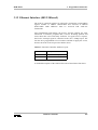
Table 5: 9-Pin Min-D Connector (male) CHAN.2 (X702)
Pin
Signal
Description
1
DCD
Data Carrier Detect
2
RxD
Receive Data
3
TxD
Transmit Data
4
DTR
Data Terminal Ready
5
GND
Signal Ground
6
DSR
Data set ready
7
RTS
Request to Send
8
CTS
Clear to Send
9
n.c.
not connected
Hardware Manual
6
9
1
5
15
1 Specification
BAB-40/60
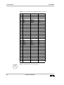
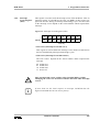
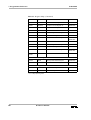
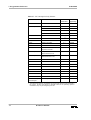
Table 6: Pin Assignment of VMEbus Connector (X101)
Pin
i
16
Row A
Row B
Row C
1
D00
/BBSY
D08
2
D01
/BCLR
D09
3
D02
/ACFAIL
D10
4
D03
/BG0IN
D11
5
D04
/BG0OUT
D12
6
D05
/BG1IN
D13
7
D06
/BG1OUT
D14
8
D07
/BG2IN
D15
9
GND
/BG2OUT
GND
10
SYSCLK
/BG3IN
/SYSFAIL
11
GND
/BG3OUT
/BERR
12
/DS1
/BR0
/SYSRESET
13
/DS0
/BR1
/LWORD
14
/WRITE
/BR2
AM5
15
GND
/BR3
A23
16
/DTACK
AM0
A22
17
GND
AM1
A21
18
/AS
AM2
A20
19
GND
AM3
A19
20
/IACK
GND
A18
21
/IACKIN
(SERCLK)
A17
22
/IACKOUT
(SERDAT)
A16
23
AM4
GND
A15
24
A07
/IRQ7
A14
25
A06
/IRQ6
A13
26
A05
/IRQ5
A12
27
A04
/IRQ4
A11
28
A03
/IRQ3
A10
29
A02
/IRQ2
A09
30
A01
/IRQ1
A08
31
-12 V
(+5STDBY)
+12 V
32
+5V
+5V
+5V
Signals in parentheses are not connected.
Hardware Manual
BAB-40/60
1 Specification
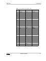
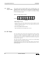
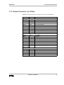
Table 7: Pin Assignment of Connector X102
Pin
Signal Row A
1
Signal Row B
Signal Row C
+5V
SCSIDB1
2
SCSIDB0
GND
SCSIDB3
3
SCSIDB2
Reserved
SCSIDB5
4
SCSIDB4
A24
SCSIDB7
5
SCSIDB6
A25
6
SCSIDBP0
A26
7
A27
8
A28
9
A29
10
A30
11
A31
12
GND
13
+5V
14
D16
15
D17
/SCSIATN
16
D18
GND
17
GND
D19
/SCSIBSY
18
/SCSIACK
D20
/SCSIRST
19
/SCSIMSG
D21
/SCSISEL
20
/SCSIC/D
D22
/SCSIREQ
21
/SCSII/O
D23
22
GND
23
D24
24
D25
25
D26
26
D27
27
D28
28
D29
29
D30
30
D31
31
GND
32
+5V
Hardware Manual
+5V
17
1 Specification
BAB-40/60
Table 8: Pin Assignment of Power Connector (X103)
Pin
Description
1
Power Good (/ACFAIL)
2
+5 V
3
+12 V
4
-12 V
5
GND
6
GND
1
18
Hardware Manual
6
BAB-40/60
1 Specification
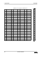
Table 9: Pin Assignment of BGB (X201)
Pin
Row A
Row B
Row C
Row D
Row E
1
GND
A08
A16
A24
TDO
2
A01
A09
A17
A25
TMS1
3
A02
A10
A18
A26
TCK
4
A03
A11
A19
A27
/TRST
5
A04
A12
A20
A28
D08
6
A05
A13
A21
A29
D09
7
A06
A14
A22
A30
D10
8
A07
A15
A23
A31
D11
9
D16
D24
64kHz
SIZE0
D12
10
D17
D25
FC1
SIZE1
D13
11
D18
D26
FC2
+5V
D14
12
D19
D27
/LIRQ1
GND
D15
13
D20
D28
/CSKBD
+12V
D00
14
D21
D29
/RESET
-12V
D01
15
D22
D30
2kHz
12VGND
D02
16
D23
D31
BCLK3
/DSACK0
D03
17
/DS
A00
GND
/HALT
D04
18
/WR
/AS
+5V
+5V
D05
19
/DSACK1
GND
/ISPEN
GND
D06
20
/BERR
16MHz
/CSGRAF
TDI
D07
E
D
C
B
A
1
2
Hardware Manual
19 20
19
1 Specification
BAB-40/60
Table 10: Pin Assignment of BEB (X222)
Pin
Signal
Pin
Signal
Pin
Signal
Pin
+12V
26
/BGACK
51
Reserved
76
/BGBEB
2
A0
27
FC2
52
+5V
77
/BERR
3
A2
28
/WR
53
D31
78
/RESET
4
A4
29
/HALT
54
D29
79
/CSBEB0
5
A6
30
/DSACK1
55
D27
80
SIZE0
6
A8
31
GND
56
D25
81
FC0
7
A10
32
D0
57
D23
82
+5V
8
A12
33
D2
58
D21
83
A31
9
A14
34
D4
59
D19
84
A29
10
GND
35
D6
60
D17
85
A27
11
A16
36
D8
61
GND
86
A25
12
A18
37
D10
62
D15
87
A23
13
A20
38
D12
63
D13
88
A21
14
A22
39
D14
64
D11
89
A19
15
A24
40
GND
65
D9
90
A17
16
A26
41
D16
66
D7
91
GND
17
A28
42
D18
67
D5
92
A15
18
A30
43
D20
68
D3
93
A13
19
+5V
44
D22
69
D1
94
A11
20
FC1
45
D24
70
GND
95
A9
21
SIZE1
46
D26
71
/IACKBEB
96
A7
22
/CSBEB1
47
D28
72
/BRBEB
97
A5
23
/DSACK0
48
D30
73
/AS
98
A3
24
/RMC
49
+5V
74
Reserved
99
A1
25
/IRQBEB
50
Reserved
75
/DS
20
Hardware Manual
100
50
51
Signal
1
100
1
-12V
BAB-40/60
1 Specification
Table 11: SCSI Connector 8-bit X103 on ADAP-200
Pin
i
Description
Pin
Description
2
DB0
28
GND
4
DB1
30
GND
6
DB2
32
ATN
8
DB3
34
GND
10
DB4
36
BSY
12
DB5
38
ACK
14
DB6
40
RST
16
DB7
42
MSG
18
DB8
44
SEL
20
GND
46
CIO
22
GND
48
REQ
24
GND
50
I/O
26
TERM-PWR
1
2
49
50
All odd pins of the 50-pin SCSI connector except pin 25 are connected to
ground. Pin 25 is left open.
Pin 26 is connected to +5 V via a Shottky diode to supply power to an
external SCSI terminator.
Hardware Manual
21
1 Specification
BAB-40/60
1.4 Definition of Board Parameters
1.4.1
VMEbus
•VMEbus interface according to specification ANSI/IEEE
STD 1014-1987 (Rev. D1.4)
•VMEbus Master Capabilities
- MD32
- MRMW8
•VMEbus Slave Capabilities:
- SADO32
- SRMW32
- UAT
- BLT
•Arbiter Options
- PRI, RRS
- BTO 4 µs to 480 µs
- SYSCLOCK generation
- BBSY filter
•Requester Options
- Any one of BR(0), BR(1), BR(2) or BR(3)
- Programmable Release when done
(RWD)
- Release-on-request
(ROR)
- Release-on-bus-clear
(ROC)
- Bus capture and hold
(BCAP)
- Programmable fair request timer 2 µs ... 30 µs.
•Interrupt Handler and Generator Capabilities
- Interrupt handler and generator on IRQ1 to IRQ7.
•Interrupter Options
- Any one of I(n) where 1 ≤ n ≤ 7.
22
Hardware Manual
BAB-40/60
1 Specification
•Address Range
- programmable extended/standard/short I/O
extended access (A31-A24 and mask)
short I/O (A15 -A8)
- Default: extended access 64 MB, short I/O 256 B
1.4.2
PCMCIA
•Two type I or II PC Cards or one type III PC Card on the front
•One type I, II, or III PC Card internal. Type III with mechnical
restrictions (see Section 2.1.2 ‘PCMCIA Installation’).
•All sockets support Flash, SRAM and ATA harddisk cards with 5 V
supply voltage.
1.4.3
Ethernet
•AUI interface according to 802.3
1.4.4
SCSI
•SCSI-2 (8 bit single ended)
•Transfer Speed
- asynchronous transfer 5 MB/s
- synchronous transfer 10 MB/s
1.4.5
Serial I/O
•2 channels (50 b/s - 38.4 kb/s)
1.4.6
MTBF Values
•8325 h (computed after MTL HDBK-217E)
•111555 h (realistic value from industry standard experience)
Hardware Manual
23
1 Specification
1.4.7
Environmental
Conditions
BAB-40/60
•Storage Temperature:
-35°C to +85°C
•Operating Temperature:
0°C to +60°C (non condensing)
•Maximum Operating Humidity:
85% relative
•Air temperature with forced air cooling of approx. 1 m/sec.
1.4.8
24
Power
Requirements
with all/max. options; approx.:
+5 VDC
±5 %
- 4.8 A max.
3.6 A typ.
- 0.5 A max.
0.3 A typ.
+12 VDC ±10 %
- 0.2 A max.
0.1 A typ.
-12 VDC ±10 %
Hardware Manual
(includes supply of
external MAU)
BAB-40/60
2 Installation
2 Installation
2.1 Introduction
•Carefully remove the board from the shipping carton.
- Save the original shipping container and packing material for storing
or reshipping the board.
Avoid touching integrated circuits except in an electrostatic free
environment. Electrostatic discharge can damage circuits or shorten
their lifetime.
•Inspect the board for any shipping damage. If undamaged, the board can
be prepared for system installation.
When unplugging boards from the rack or otherwise handling
boards, do always observe precautions for handling electrostatic
devices.
Since upgrading the BAB-40 to BAB-60 requires some additional
components, it is not recommended that this is done by the user.
Please contact ELTEC.
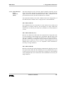
2.1.1
SIMM
Installation
Generally all PS/2 SIMMs from 1 MB to 32 MB with symmetric
RAS/CAS addresses and better than 70 ns access time are suitable for the
BAB-40/60. Since the BAB-40/60 does not use parity checking, SIMMs
with or without parity can be used, but SIMMs without parity should be
preferred because they are usually cheaper and smaller. It is mandatory
that the length of the SIMM board does not exceed 35 mm to fit on the
BAB-40/60.
Hardware Manual
25
2 Installation
BAB-40/60
Table 12: Recommended SIMMs
SIMM Size
!
Chip Size
No. of Chips
Chip
Organization
No. of Banks
(RAS)
1 MB
1M
8
256Kx4
single
1 MB
4M
2
256Kx16
single
1 MB
4M
2
256Kx18
single
2 MB
1M
16
256Kx4
double
2 MB
4M
4
256Kx16
double
2 MB
4M
4
256Kx18
double
4 MB
4M
8
1Mx4
single
4 MB
16 M
2
1Mx16
single
8 MB
4M
16
1Mx4
double
8 MB
16 M
4
1Mx16
double
16 MB
16 M
8
4Mx4
single
32 MB
16 M
16
4Mx4
double
Before removing or installing the SIMM module switch power off.
The SIMM is simply plugged into the connector (it fits only in one
orientation) and is automatically recognized by the RMon (please check
the power-on message of the RMon). If RMon hangs with '5' in the LED
display or reports the wrong size, installation was not correct or the SIMM
is not suitable for the BAB-40/60.
!
26
Although the BAB-40/60 RAM design has been optimized for
compatibility, layout of the SIMM's PCB and the type of the RAM
chips may affect reliability. Therefore, ELTEC can't guarantee
operation with all available SIMM modules. It is recommended to use
SIMMs of well-known manufacturers (Fujitsu, Hitachi, Toshiba,
Samsung, TI, ...).
Hardware Manual
BAB-40/60
2.1.2
2 Installation
PCMCIA
Installation
The PC Cards can easily be plugged into one of the three sockets when
they have the right orientation. To avoid unintended removal of the PC
Cards on the front they can be locked with a metal plate and two screws
M3x6. The internal PC Card can also be fixed to withstand shock and
vibration. For correct distance of the PC Card and the PCB, a washer is
necessary between the PCB and the holder.
Figure 2: PCMCIA Installation
Holder
PC Card
Washer
PCB
Screw M2.5 x 6
!
Live insertion and removal of PC Cards is possible while none of the
PC Cards is accessed by the CPU. Since it is not easy to satisfy this
condition it is recommended to avoid live insertion and removal.
!
When a type III PC Card is installed in the internal socket, the
VMEbus specification of the adjacent VMEbus slot is violated so that
it must stay free.
!
Not all type III PC Cards fit into the internal socket. Only 5 V supply
voltage cards are supported. For a detailed list of cards and drivers,
please contact ELTEC.
Hardware Manual
27
2 Installation
2.1.3
Board
Installation
BAB-40/60
The installation of the BAB-40/60 on VMEbus is not complicated. A
suitably terminated VMEbus backplane is required. The power supply
must meet the specifications described in Section 1.4 ‘Definition of Board
Parameters’. The processor board requires +5 V supply voltage; ±12 V are
needed for the RS 232 serial interface and the Ethernet interface.
2.1.3.1 Serial
RMon uses CHAN.1 of the SCC. V-CABL-A144 can be used to connect a
terminal (9600 baud, 8 bit, 1 stop bit, no parity) via X701 to the
BAB-40/60.
2.1.3.2 Graphics
If a graphics module is installed, it requires a VGA monitor and ATkeyboard with PS/2 connector. A standard VGA monitor has to be
connected to the 15-pin Sub-D female connector and the keyboard has to
be connected to 6-pin female miniature circular (mini-DIN) connector.
Both connectors are located on the front panel. A standard VGA monitor
and a standard PS/2 compatible keyboard fit without modification. For
connection to an AT-keyboard, ADAP-210 is available.
2.1.4
The Serial Interface Level Converter (SILC) modules generally convert
TTL-level signals generated or accepted by the SCC to the appropriate
signal levels for external transmission lines. SILC modules for RS 232,
RS 422 and RS 485 are available.
Serial Interface
Level
Converter
(SILC)
The mechanical outline of the SILC modules allows the changeability of
the different SILC modules on the BAB-40/60.
•SILC-200 for RS 232
•SILC-300 for RS 422
•SILC-400 for RS 485
The mechanical part of the installation is very easy. First switch off the
VMEbus system and pull the board out of the rack. If a SILC module is
already placed in the connector, remove it carefully. Now plug the new
SILC module into the corresponding connector on the CPU or I/O board.
Consider the polarization of the SILC module. To avoid damage, check
that the pin 1 marked on the back of the SILC fits to pin 1 marked on the
board.
28
Hardware Manual
BAB-40/60
2 Installation
2.1.5
Ethernet
Installation
A standard Ethernet/Cheapernet MAU or a CONV-500 Cheapernet/
10BaseT MAU can be connected via AUI cable to the 15-pin AUI
connector on the front panel of the BAB-40/60. The length of the AUI
cable is limited to 50 m. For connections up to about 2 m, flat cable can
also be used. In order to avoid HF radiation, this cable should be shielded.
2.1.6
SCSI
Installation
A 8-bit SCSI bus can be connected to X103 of ADAP-200. If the
BAB-40/60 is located at either end of the SCSI bus, the termination must
be enabled in the RMon setup menu, otherwise it must be disabled.
Hardware Manual
29
2 Installation
BAB-40/60
Figure 3: Installation Diagram
S902
S901
U903
X702
X701
X801
VGA
Keyboard
X1101
30
Hardware Manual
BAB-40/60
2 Installation
2.2 Default Board Setting
Table 13: Default Settings
Jumpers/Switches
Position
Description
J301
closed
System controller enabled. See Section 2.3.1
‘
System Controller (J301)’
.
J701
1-2
DCD from X702 connected to SILC. See
Section 2.3.2
‘
Serial
Interface
CHAN.2
Configuration’
.
J702
1-2
3-4
DCD from SILC connected to SCC
7.37 MHz connected to SCC receive clock.
See Section 2.3.2 ‘
Serial Interface CHAN.2
Configuration’
J703
1-2
DTR from SCC connected to SILC.
See Section 2.3.2 ‘
Serial Interface
Configuration’
.
CHAN.2
J1401
open
No reset. See Section 2.3.3 ‘
Reset (J1401)’
.
J1605
1-2
See Section 2.3.4 ‘
Pin 1 Connection of EPROM
(J1605)’
J1702
closed
Write enable for serial EEPROM, seeSection 2.3.5
‘
EEPROM Write Enable (J1702)’
S901
0
VMEbus slave address at $8000.0000, see
Section 2.3.6.1 ‘
VMEbus Slave Address (S901)’
S902
0
Default initialization values, see Section 2.3.6.2
‘
Hardware Configuration (S902)’
Hardware Manual
31
2 Installation
BAB-40/60
Figure 4: Location of Jumpers, Interface Connectors and Switches
32
Hardware Manual
BAB-40/60
2 Installation
2.3 Jumpers and Switches
This section lists all features user-selectable by jumpers and switches. For
details, refer to the appropriate descriptions identified in parentheses.
All settings on a dark grey background (
) indicate default settings.
The BAB-40/60 operates as single board computer in this configuration.
There are only very few jumpers on the BAB-40/60 which typically need
no changes after shipping. All other parameters are software
programmable. Since the jumper connections are not changed easily, it is
strongly recommended that these changes are performed by qualified
personal only.
The user should refer to the silkscreen print on the component side of the
BAB-40/60 for the following guidance on jumper area pin identification.
Pin 1 of every jumper area is marked by a beveled corner on the silkscreen
outline of the jumper. If you see this corner at the left upper side of the
jumper area, then pin 2 is on the right-hand side of pin 1. Pin 3 can be
found on the right of pin 2, and so on.
2.3.1
System
Controller
(J301)
Table 14: J301 (System Controller)
Jumper J301
open
closed
2.3.2
Serial Interface
CHAN.2
Configuration
Function
System controller disabled
System controller enabled
Table 15: J701 (CHAN.2 DCD/DSR Select)
Jumper J701
Function
1-2
DCD of X702 connected to SILC
2-3
DSR of X702 connected to SILC
Table 16: J702 (CHAN.2 DCD/Receive Clock Select)
Jumper J702
Function
1-2
DCD/DSR from SILC connected to DCD of SCC
2-3
DCD/DSR from SILC connected to receive clock of SCC
3-4
7.37 MHz connected to receive clock of SCC
Hardware Manual
33
2 Installation
BAB-40/60
Table 17: J703 (DTR/Transmit Clock Select)
Jumper J703
Function
1-2
DTR of SCC is connected to SILC
2-3
Transmit clock of SCC is connected to SILC
Figure 5: Serial Interface CHAN.2 Configuration
SCC
9-pin Sub-D
SILC
5 MHz
PCLK
TxD
TxD
RxD
RxD
RTS
RTS
CTS
CTS
3
TxD
2
RxD
7
RTS
8
CTS
4
DTR
6
nc
1
DCD
9
nc
5
GND
J703
DTR
DCD
SYNC
TRxC
RTxC
DTR
1
2
3
J701
3
2
J702
1
2
DSR
DCD
1
RI
3
4
+
GND
W/REQ
PC
7.3728 MHz
34
Hardware Manual
BAB-40/60
with
SILC-200
BAB-40/60
2.3.3
Reset (J1401)
2 Installation
When J1401 is closed or an external switch is connected to J1401, reset
can be generated.
Table 18: J1401 (Reset)
Jumper J1401
2.3.4
Pin 1
Connection of
EPROM
(J1605)
open
Normal operation
closed
Reset
This jumper allows to select between EPROMs up to 4 Mbit and 8 Mbit.
Table 19: J1605 (Pin 1 Connection of EPROM)
Jumper J1605
2.3.5
EEPROM
Write Enable
(J1702)
Function
Function
1-2
Pin 1 connected to +5 V (< 8 Mbit)
2-3
Pin 1 connected to A19 (8 Mbit)
J1702 enables/disables the hardware write protection for the serial
EEPROM. Only the upper 256 B of the EEPROM can be write protected.
Table 20: J1702 (EEPROM Write Enable)
Jumper J1702
open
closed
2.3.6
Function
Write protection enabled
Write protection disabled
Switches
Both hex switches (S901, S902) are used by RMon for the configuration
setup (see RMon manual). They are connected to port B of the CIO.
2.3.6.1 VMEbus Slave
Address (S901)
The hex switch S901 selects the BAB-40/60 slave window address. The
size of the A32 slave window is normally 256 MB. This can be changed
by the RMon setup menu. The size of the A16 slave window (used for
VIC access) is 256 bytes.
Hardware Manual
35
2 Installation
BAB-40/60
Table 21: Hex Switch S901 (VMEbus Slave Address)
Hex Switch
S901
2.3.6.2 Hardware
Configuration
(S902)
VMEbus Base Address
A32
A16
F
$F000.0000
$F000
E
$E000.0000
$E000
D
$D000.0000
$D000
.
.
.
1
$1000.0000
$1000
0
Use configuration value
Switch S902 defines the configuration source and the operation mode. For
switch position 0, 1, RMon enters an interactive mode. If switch S902 is in
position 8 to F, the user program located in the RMon EPROM is called.
Table 22: Hex Switch S902 (Hardware Configuration)
Hex Switch
S902
i
36
Function
0
Hardware configuration from basic EPROM
1
Hardware configuration from SRAM
2
Reserved for ELTEC
3
RMon interactive mode on serial port
4
RMon interactive mode on dual-ported RAM
(local address $C000)
5-7
Reserved for ELTEC
8-F
Hardware configuration from SRAM and start program in user EPROM
S901 and S902 have no direct influence. A changed position becomes only
effective after the next reset (i.e. the software reads the switches and
programs the appropriate registers).
Hardware Manual
BAB-40/60
3 Programmers Reference
3 Programmers Reference
3.1 Address Map
The BAB-40/60 is designed to utilize the entire 4 GB address range of the
68040/060 chip. Using the address modifier of the VMEbus, the address
range may be enlarged by subdivision into data and program areas and / or
user and supervisor areas. The BAB-40/60 recognizes two address areas:
the local address space and the global VMEbus address space.
Table 23: Address Assignment of BAB-40/60
VMEbus
Address Modifier
Cache 1)
Burst 2)
Local RAM
local
Y
Y
32
$0200.0000 - $03FF.FFFF
Local RAM (mirrored)
local
N
Y
32
$0400.0000 - $05FF.FFFF
Video RAM
local
Y
N
32
$0600.0000 - $07FF.FFFF
Video RAM (mirrored)
local
N
Y
32
N
32/16/8
Address Range
Device
$0000.0000 - $01FF. FFFF
Access
Width [b]
$0800.0000 - $FBFF.FFFF
VMEbus Extended
A32
N3)
$FC00.0000 - $FC3F.FFFF
PCMCIA1
local
N
N
16/8
$FC40.0000 - $FC7F.FFFF
PCMCIA2
local
N
N
16/8
$FC80.0000 - $FCBF.FFFF
PCMCIA0
local
N
N
16/8
$FCC0.0000 - $FCFF.FFFF
Reserved
-
-
-
-
$FD00.0000 - $FDFF.FFFF
BEB0
local
N
N
32/16/8
$FE00.0000 - $FE7F.FFFF
BEB1
local
N
N
32/16/8
$FE80.0000 - $FEBF.FFFF
EPROM
local
Y
N
8
$FEC0.0000 - $FECF.FFFF
Local I/O
local
N
N
32/16/8
$FED0.0000 - $FEFF.FFFF
Reserved
-
-
-
-
$FF00.0000 - $FFFE.FFFF
VMEbus Standard I/O
A24
N
N
32/16/8
$FFFF.0000 - $FFFF.FFFF
VMEbus Short I/O
A16
N
N
16/8
1. Y = /TCI driven high, N = /TCI driven low.
2. Y = /TBI driven high, N = /TBI driven low.
3. Caching may be enabled via system control register.
Hardware Manual
37
3 Programmers Reference
BAB-40/60
Table 24: Local I/O Address Assignment for BAB-40/60
Address
38
Device
Size
Access
$FEC0.0000 - $FEC0.7FFF
VIC (D0..7)
byte
read/write
$FEC0.8000 - $FEC0.FFFF
VMEbus Decoder (D0..31)
see Section 3.2.2 ‘
RAM Access
from the VMEbus’
lword
write
$FEC1.0000 - $FEC1.FFFF
Reserved
-
-
$FEC2.0000 - $FEC2.FFFF
NVRAM/RTC
byte
read/write
$FEC3.0000 - $FEC3.FFFF
System CIO
byte
read/write
$FEC4.0000 - $FEC4.FFFF
Reserved
-
-
$FEC5.0000 - $FEC5.3FFF
Watchdog
byte
read/write
$FEC5.4000 - $FEC5.7FFF
Revision EEPROM
byte
read
$FEC5.8000 - $FEC5.BFFF
Reserved
$FEC5.C000 - $FEC5.DFFF
Enable slave select (ESR)
see Section 3.2.2 ‘
RAM Access
from the VMEbus’
byte
write
$FEC5.E000 - $FEC5.FFFF
Snoop Control Register
byte
write
$FEC6.0000 - $FEC6.3FFF
Keyboard and Video Controller
byte
read/write
$FEC6.4000 - $FEC6.7FFF
Serial I/O
byte
read/write
$FEC6.8000 - $FEC6.BFFF
ILACC
lword
read/write
$FEC6.C000 - $FEC6.FFFF
SCSI Controller
lword
read/write
$FEC7.0000 - $FEC7.FFFF
IOC-2
lword
read/write
$FEC8.0000 - $FECF.FFFF
Reserved
-
-
Hardware Manual
BAB-40/60
3 Programmers Reference
3.2 DRAM
3.2.1
RAM Access
from the Local
CPU
i
3.2.2
RAM Access
from the
VMEbus
The base address of the DRAM is fixed to $0000.0000.
After reset, the EPROM is mapped to address $0000.0000. After some
initialization the firmware enables the DRAM at $0000.0000 via PA5 of
the system CIO.
The base address for VMEbus access is specified by the slave base
address register (SBR) and the enable slave select register (ESR) of the
BAB-40/60. The SBR is only accessible by the local CPUs by longword
write cycles. The SBR is undefined after reset and has to be written before
the BAB-40/60 can be accessed from the VMEbus. The ESR is cleared
(disabling all slave accesses) by power-on reset and the reset switch. The
ESR can only be accessed by byte write cycles.
Table 25: Slave Base Address Register Layout
!
Register
Address
31
24
SBR
$FEC0.80F4
A32
Decoder
ext. access
23
16
unused
15
ICF
Decoder
short I/O
8
7
0
unused
Do not use other addresses for the SBR register.
The A32 decoder compares A31 to A24 of the VMEbus with the SBR bits
32 to 24 for VMEbus extended access.
Hardware Manual
39
3 Programmers Reference
BAB-40/60
The ICF1 decoder compares A15 to A8 of the VMEbus with the SBR bits
15 to 8. The ESR register allows separate enabling of the two
comparators.
Table 26: Enable Slave Register Layout
Reg.
Address
ESR
$FEC5.C000
7
...
3
unused
2
1
0
ICF1 (A16)
unused
VEXT (A32)
1 = Decoder enabled
0 = Decoder disabled
3.2.3
Address
Translation
The address presented by the VMEbus, the BEB, or the ILACC is
translated from the '020 bus (A 020) to the ‘040 bus (A 040) with the help of
the MBAR (memory base address register) and ASR (address substitution
register) of the IOC-2. The address on the ‘040 bus is calculated using the
following formula:
A040 = (MBAR & ASR) + (A 020 & /ASR)
&
logical AND operation,
+
logical OR operation,
/
logical complement.
The translation is necessary for snooping of the CPU to keep its caches
consistent with the memory.
The translated address must always be in the DRAM. If not, the
computer crashes in most cases. For all address lines not driven by the
source the corresponding bit position in the ASR must be 1 so that the
invalid bits are substituted.
Unfortunately the address translation exists only once for the three address
sources (VMEbus, BEB, ILACC). This leads to some restrictions when
the DRAM is accessed by A24 addressing from the BEB. In this case only
parts of the DRAM can be reached by VMEbus A32 addressing or the
ILACC.
i
40
To avoid problems, ELTEC recommends that DMA BEB boards should
deliver at least A0 to A26 for operation with the default configuration.
Hardware Manual
BAB-40/60
3 Programmers Reference
3.2.4
RAM Mirror
In some cases it may be desirable to prevent caching of data that are
shared with other devices (BEB, VMEbus, ILACC). In these cases the
cache inhibited RAM mirror can be used.
3.2.5
RAM Access
from the BEB
Access from the BAB Extension Bus (BEB) is done by using a standard
68k-like requester with three-line handshake (/BR, /BG, /BGACK ).
During master transfers from the BEB a minimum of 24 address lines
(A0 - A23) have to be driven. For operation with the default configuration
(64 MB slave window) at least A0 to A26 have to be driven (see
Section 3.2.3 ‘Address Translation’).
3.2.6
RAM Access
from ILACC
The AM79C900 Ethernet Controller uses DMA transfer cycles to transfer
commands, data and status information to and from the DRAM.
Hardware Manual
41
3 Programmers Reference
BAB-40/60
3.3 VMEbus Interface
Each BAB-40/60 has a VMEbus master and a VMEbus slave interface.
Additionally, VMEbus system controller functions are available via the
VMEbus gate array (VIC) used on the BAB-40/60 board.
3.3.1
System
Controller
The BAB-40/60 features a full slot-one system controller, including
SYSCLK , SYSRESET, bus time-out, IACK daisy chain driver, and a four
level arbitration circuit. System controller capabilities are enabled by
inserting jumper J301.
SYSCLK
The SYSCLK is always driven if the system
controller is enabled.
SYSRESET
A low level on this signal resets the internal logic
and asserts the local reset for a minimum of
200 ms. If the VIC is configured as system
controller, the reset switch on the front panel (S4)
asserts the SYSRESET for a minimum of 200 ms.
Writing a $F0 to the system reset register of the
VIC at address $FEC0.10E3 resets all registers of
the VIC and asserts the SYSRESET output for a
minimum of 200 ms.
BTO
The VIC includes two independent bus time-out
modules (BTO) for local cycles and for VMEbus
cycles. The VMEbus time-out is only enabled when
the VIC is configured as system controller. On VIC
reset, the VMEbus time-out period is set to 64 µs
and the local bus time-out period to 32 µs. This can
be altered by programming the transfer time-out
register of the VIC at address $FEC0.10A3. Use the
RMon setup menu to change this value.
Four Level Arbiter If the VIC is configured as system controller, the
four level arbiter is enabled and programmed by
writing into the arbiter / requester configuration
register at address $FEC0.10B3. Use the RMon
setup menu to change this value.
42
Hardware Manual
BAB-40/60
3.3.2
3 Programmers Reference
VMEbus
Master
Interface
The master interface of the BAB-40/60 board supports 8, 16, and 32-bit
data transfer cycles in A32, A24, and A16 addressing modes. For a short
overview, see Section 1.4 ‘Definition of Board Parameters’.
3.3.2.1 Longword
Access to
Wordwide
Slaves
Two different control lines of the system CIO enable longword breaking
for the A32 and A24/A16 area:
PA3: * 0 : forces A24(A16)/D16 data size on VMEbus
1 : allows A24(A16)/D32 data size on VMEbus
PA4: * 0 : allows A32/D32 data size on VMEbus
1 : forces A32/D16 data size on VMEbus
* specifies the default values set by RMon.
Use the RMon setup menu for changes.
3.3.2.2 Address
Modifier Source
The VIC chip supplies the VMEbus address modifier signals. This is done
by either routing FC0..2 line to AM0..2, or by driving these signals by an
internal address modifier source register of the VIC ($FEC0.10B7). The
AM3..5 lines are driven depending on the actual data size, or by the
address modifier source register. One CIO output signal is used to control
this option:
PA2: * 0 : uses CPU and address size dependent modifiers
1 : uses VIC’s address modifier source register
* specifies the default values set by RMon.
Use the RMon setup menu for changes.
For a detailed description of the address modifier values, see Section A.2
‘Address Modifiers on VMEbus’.
3.3.2.3 Read-ModifyWrite Cycles
!
Read-modify-write cycles, like TAS or CAS2 are supported by the
BAB-40/60.
The CAS2 instruction has only limited support (see Table 1: ‘CAS2
Operations on the Various Busses’). The easiest way to ensure that
CAS2 instructions are indivisible is to have both operands of the
CAS2 instruction within the same memory area (local RAM,
VMEbus, BEB).
Hardware Manual
43
3 Programmers Reference
3.3.2.4 A16 Slave
Interface
(ICMS)
BAB-40/60
A very useful feature of the VIC is a set of registers and switches for
message passing or event signaling.
There are eight bytewide general-purpose interprocessor communication
registers accessible from the VMEbus or the local bus (CPU).
•Registers 0 to 4 are general-purpose dual-port registers.
•Register 5 is a dual-port read-only ID register to identify the VIC and its
revision level.
•Register 6 is a module status register which is read-only from the
VMEbus.
•Register 7 provides semaphores for registers 0-4 and several system
control functions like a remote reset function.
Four ‘Interprocessor Communication Module Switches’ (ICMS) are
provided by the VIC. These are bytewide mailbox switches to signal
events by generating an interrupt to the local CPU if accessed from the
VMEbus. To signal dedicated events/messages the ICMS locate a unique
set of addresses.
The intercommunication registers within the VIC chip are accessible in
A16 VMEbus address space only.
For programming the ICF decoder registers, see the description of the
slave base address register, slave mask register and enable slave select
register in Section 3.2.2 ‘RAM Access from the VMEbus’.
Use the RMon setup menu to change the register values. Within the
256-byte space the VIC chip locates several intercommunication registers.
Table 27: Intercommunication Register Location on VMEbus
Register Type
A07
06
05
04
03
02
01
AM5..0
Interprocessor Communication
Registers
X
X
0
0
#
#
#
$2D
Interprocessor Communication
Global Switches
X
X
0
1
0
#
#
$2D
Interprocessor Communication
Module Switches
X
X
1
0
0
#
#
$2D or
$29
X : don’
t care.
# : selects register/switch number.
For further information, refer to the VIC068 data sheet.
44
Hardware Manual
BAB-40/60
3 Programmers Reference
3.4 PCMCIA Interface
3.4.1
Interface
Description
3.4.2
Address Range
The PCMCIA was designed for extension cards on laptop computers. It
offers 64 MB of attribute memory, common memory and I/O. The
PCMCIA interface converts CPU signals to PCMCIA signals via PLD.
Memory, I/O and mixed cards can be used. The address and data lines are
connected via buffers to the card connector. 10 kΩ pull-ups are connected
to the data lines to define a $FF on the data bus if no device on the card is
selected. The access time to the card is at least 200 ns and can be extended
to up to 12 µs by using the - WAIT signal. The interface supports the
dynamic data bus sizing. Longword transfers of the CPU are automatically
converted into two word or four byte accesses on the PCMCIA card
depending on the address space and the -IOCS16 signal. Pin 16 of the card
interface is routed to the IRQ3 pin of the VIC. This pin can be used as
interrupt request (-IREQ) for I/O cards or to support +RDY/-BSY
handshake in memory applications. The +RESET signal is generated
depending on the CPU reset signal and bit 3 of the control register. Status
change, battery voltage detect, card detect and other features are supported
by using control registers.
The standard address window for one PCMCIA socket on ELTEC’s CPU
boards offers 4 MB. The PCMCIA uses the following relative address
space:
Figure 6: Relative Address Space
Relative Address
Access to
$40.0000
Socket config.
I/O
PCMCIA I/O
I/O
common
or
attribute
MEMORY
$30.0000
$20.0000
$00.0000
Hardware Manual
45
3 Programmers Reference
BAB-40/60
The PCMCIA interface offers four configuration registers.
Figure 7: PCMCIA Interface Configuration Registers
Relative Address
3.4.3
Card Control
Register (CCR)
Access to
$30.0001
Card Control Register (CCR)
$34.0001
Card Status Register (CSR)
$38.0001
Interrupt Vector Register (IVR)
$3C.0000
Window Register (WIR)
This register is used to select the PCMCIA command timing, V pp voltage,
and to control the state of the RESET.
Figure 8: Card Control Register (CCR)
$30.0001
7
6
5
4
3
2
1
0
IEN
CT1
CT2
Vpp
RST
1
1
1
read and write
•IEN
Enable socket interrupt request.
•CT1 and CT2 (Command Timing)
These bits are used to define the minimum command pulse width to the
socket interface. The write pulse is one clock shorter than the read pulse.
This is done to generate a longer data hold time for write cycles to the
socket interface. For read cycles, the card should be driven valid data
one clock before the read command becomes inactive. The complete
cycle time (setup + command + recover) for read and write accesses is
identical.
46
Hardware Manual
BAB-40/60
3 Programmers Reference
Figure 9: Timing
setup
command
recovery
A(x)
-REG
-CE(x)
-IO16
-IOR
-OE
D(x)
read
-IOW
-WE
D(x)
write
Command Timing
-IOR or -OR
-IOW or -WE
CT1
CT2
1
1
120 ns
80 ns
1
0
280 ns
240 ns
0
1
440 ns
400 ns
0
0
600 ns
560 ns
The default reset value is '11'. The setup and recovery timings are
depending on the base board. The absolute minimum timings are:
Read setup
Read recovery
Write setup
Write recovery
> 60 ns
> 20 ns
> 60 ns
> 60 ns
•Vpp (V pp Enable)
This bit is used to switch the V pp voltage of the socket interface from
+5 V to +12 V. The default reset value is +5 V ('0').
•RST (Reset)
This bit is used to control the +RESET of the card interface and the
output enable of the Window Register (WIR). Default reset value is '1'.
Hardware Manual
47
3 Programmers Reference
3.4.4
Card Status
Register (CSR)
BAB-40/60
This register reflects the status of the PCMCIA interface. Ready, Write
Protect, Card Detect, and Battery Status is available from this register.
Figure 10: Card Status Register (CSR)
$34.0001
7
6
5
4
3
2
1
0
RDY
WP
CD
BV2
BV1
1
1
1
read only
•RDY (Ready - Interrupt Request)
This bit reflects the state of the RDY-IREQ pin of the socket. In memory
mode, this input indicates the ready-busy state of the card. In I/O mode,
it indicates an interrupt request.
•WP (Write Protect - I/O select 16)
This bit reflects the state of the WP-IO16 pin of the socket. In memory
mode, this input is the status of the write protect switch of the card. In
I/O mode, it indicates that the I/O address being accessed is capable of
16-bit operation.
•CD (Card Detect)
If this bit is set to '0', it indicates the presence of a card in the socket.
•BV2 (Battery Voltage 2)
In memory mode this bit serves as the BVD2 (battery warning status). In
DMA mode it may be used for DMA request.
•BV1 (Battery Voltage 1)
In memory mode this bit serves as the BVD1 (battery dead status). In
I/O mode, this is the STSCHG (card internal status change).
48
Hardware Manual
BAB-40/60
3.4.5
3 Programmers Reference
Interrupt
Vector Register
(IVR)
This register is used to select the interrupt vector of the PCMCIA. After an
interrupt request of a PCMCIA card, the six MSBs of this register are
passed to the CPU during an interrupt acknowledge cycle. The two LSBs
of the interrupt vector depend on the socket number which requested the
interrupt.
Figure 11: Interrupt Vector Register (IVR)
$38.0001
7
6
5
4
3
2
1
0
IV7
IV6
IV5
IV4
IV3
IV2
IV1
IV0
write only
•IV2 to IV7 (Interrupt Vector Bit 2 to 7)
This register is used to define the interrupt vector which is transferred to
the base board during interrupt acknowledge cycles.
•IV0 to IV1 (Interrupt Vector Bit 0 and 1)
The bits 0 and 1 depend on the socket number which requested the
interrupt.
00
01
10
11
!
i
PCMCIA1
PCMCIA2
PCMCIA0
Reserved
Only one interrupt vector register exists for all PCMCIA sockets.
Changing the vector for one socket will also affect the other interrupt
vectors.
If more than one PC Card requests an interrupt, PCMCIA0 has the
highest and PCMCIA1 has the lowest priority.
Hardware Manual
49
3 Programmers Reference
3.4.6
Window
Register (WIR)
BAB-40/60
This register selects the higher address lines, the REG signal of the
PCMCIA interface. The output enable of this register is controlled by the
RST bit the CCR. If RST is active ('1'), the output of the WIR is disabled.
REG is driven to '1', A21 to A25 are '0'. If RST is '0', the WIR is enabled
to drive the PCMCIA signals.
Figure 12: Window Register (WIR)
$3C.0000
7
6
5
4
3
2
1
0
REG
-
A25
A24
A23
A22
A21
-
write only
•REG (Register Access)
During memory cycles, this output chooses between attribute (0) and
common (1) memory. During I/O cycles, this signal switches between
I/O (0) and DMA (1) access.
•A21 to A25 (Address Lines 21 to 25)
These bits define the socket address lines 21 to 25.
3.5 VIC Timer
The VIC contains a timer which can be programmed to output a periodic
wave form on LIRQ2. The frequencies available are 50 Hz, 100 Hz, and
1000 Hz. The timer is enabled and controlled by writing slave select
control register 0. The interrupt is enabled and controlled by writing local
interrupt control register 2.
The clock tick timer is typically used as a time base for multi-tasking
operating systems, such as OS-9 or LynxOS.
If other frequencies are needed, one of the three counters / timers that are
included in the CIO may be used. For more details about the timer, refer to
the VIC data sheet.
50
Hardware Manual
BAB-40/60
3 Programmers Reference
3.6 Battery-Backed Parameter RAM and Real-Time Clock
The real-time clock is designed with the MK48T12 or MK48T18
timekeeper RAM from SGS Thomson or DS1644 from Dallas. The chip
combines a 2KBx8 (8KBx8, 32KBx8) CMOS SRAM (parameter RAM) a
bytewide accessible real-time clock, a crystal, and a long life lithium
battery, all in one package. The MK48Txx devices have a battery lifetime
of approximately 3.7 years when the clock oscillator is running. To extend
battery lifetime, the clock oscillator can be stopped. Alternatively a Dallas
DS1642/1643 device can be used, which offers a lifetime of 10 years even
if the oscillator is running.
3.6.1
Parameter
RAM
(NVRAM)
The address area of this SRAM is divided into two main parts:
•system dependent parameter data structure, defined by ELTEC to store
setup parameters for hardware initialization and boot informations for
operating systems,
•eight bytes of the SRAM for the registers of the real-time clock.
Table 28: Address Assignment of SRAM/RTC
Address
Description
$FEC2.0000 - $FEC2.07F7
Reserved for system configuration values.
The structure of the system configuration values is
defined in the RMon manual.
$FEC2.07F8 - $FEC2.7FF7
Free for user data if DS1644 is installed.
$FEC2.7FF8 - $FEC2.7FFF
Real-time clock registers. See Section 3.6.2 ‘
Real-Time
Clock’for more information.
The S902 hex switch position '0' uses the configuration values stored in
the basic EPROM rather than values defined in the SRAM. For more
details, see also the RMon description.
!
If a MK48T18 is installed, J1602 must be changed from position 1-2
to 2-3. If a DS1644 is installed, J1602 must be changed from position
1-2 to 2-3. Additionally, J1606, J1607 must be closed and R1602 must
be removed. The Dallas timekeeper RAMs do not offer the feature to
check the battery. The SGS Thomson devices allow to check an
internal battery OK flag.
Hardware Manual
51
3 Programmers Reference
3.6.2
Real-Time
Clock
BAB-40/60
The clock features BCD-coded year, month, day, hours, minutes, and
seconds as well as a software controlled calibration. For lifetime
calculations of the battery, please refer to the data sheet.
Access to the clock is as simple as conventional bytewide RAM access
because the RAM and the clock are combined in the same chip.
Table 29: Address Assignment of the Real-Time Clock
MK48T12 Address
Description
$FEC2.7FF8
RTC Control Register
$FEC2.7FF9
Seconds
$FEC2.7FFA
Minutes
$FEC2.7FFB
Hour
$FEC2.7FFC
Day
$FEC2.7FFD
Date
$FEC2.7FFE
Month
$FEC2.7FFF
Year
For further details, see the MK48T12/MK48T18 resp. DS1644 data sheet.
i
52
The SRAM/RTC can only be accessed with byte instructions.
Hardware Manual
BAB-40/60
3 Programmers Reference
3.7 CIO Counter / Timer
The BAB-40/60 offers three independent, programmable 16-bit
counter / timers integrated in the CIO.
Table 30: Address Assignment of the System CIO
Address
Description
$FEC3.0000
Port C Data Register CIO (Status Display)
$FEC3.0001
Port B Data Register CIO (Hex Switches)
$FEC3.0002
Port A Data Register CIO (System Control Register)
$FEC3.0003
Control Register CIO
The peripheral clock of the CIO is connected to a 5 MHz source. The
interrupt request outputs of CIO is connected to the LIRQ6 input of the
VIC. Local interrupt control register 6 (LIRQ6) of the VIC has to be
programmed for an active low, level-sensitive input. The vector is
supplied by the CIO. The VIC has to be programmed to generate
interrupts on level 6 to the CPU. Only CPU IACK level 6 cycles are
routed to the CIO device.
Hardware Manual
53
3 Programmers Reference
BAB-40/60
3.8 Watchdog Timer
The watchdog timer installed on the BAB-40/60 monitors the activity of
the microprocessor. If the microprocessor does not write location
$FEC5.0000 within a certain time-out period, a reset pulse is generated.
After reset, the watchdog timer is disabled.
The watchdog becomes active after writing the desired time-out period to
the watchdog configuration register at $FEC5.2000. Also the watchdog
has a lock feature. When locked, the watchdog configuration register
cannot be changed anymore to prevent unintentionally altering the
watchdog period. Only reset is able to unlock the watchdog.
After reset the software can read port A bit 7 of the system CIO to
distinguish between a watchdog reset (PA7 = ‘0’) and a reset generated by
other sources (PA7 = ‘1’). This watchdog indicator is cleared by power-up
reset, the reset switch, a VMEbus SYSRESET , a VIC remote reset, or by a
write access to address $FEC5.0000.
Table 31: Address Assignment of Watchdog Registers
54
Address
Description
Access
Direction
$FEC3.0002
Port A Data Register System CIO
read PA7
$FEC5.0000
Watchdog Trigger
write
$FEC5.2000
Watchdog Configuration
write
Hardware Manual
BAB-40/60
3 Programmers Reference
Table 32: Watchdog Configuration Register at $FEC5.2000
Value
Function
$00
Disable Watchdog
$01
Enable Watchdog 130 ms
$02
Enable Watchdog 260 ms
$03
Enable Watchdog 520 ms
$04
Enable Watchdog 1.04 s
$05
Enable Watchdog 2.08 s
$06
Enable Watchdog 4.16 s
$07
Enable Watchdog 8.32 s
$08
Enable Watchdog 16.64 s
$09
Enable Watchdog 33.28 s
$0A
Enable Watchdog 1 min 6 s
$0B
Enable Watchdog 2 min 13 s
$0C
Enable Watchdog 4 min 26 s
$0D
Enable Watchdog 8 min 52 s
$0E
Enable Watchdog 17 min 44 s
$0F
Reserved (Watchdog disabled)
$10 - S1F
Same as $00 - $0F but watchdog becomes locked
Hardware Manual
55
3 Programmers Reference
BAB-40/60
3.9 Revision Information
Revision information is stored on the board to give software the chance to
distinguish between different versions and derivates of the BAB-40/60.
The information consists of two parts. First there are bits 3-7 of the
IOC-2’s control register at $FEC7.00A8.
Table 33: IOC-2 Control Register at $FEC7.00A8
Register
ICR
Address
$FEC7.00A8
31 - 8
7-5
4
3
used for IOC-2
internal
purposes
000
2-0
ELTEC initial version
0
0
25 MHz
001
EUROCOM-17-1xx/2xx
0
1
33 MHz
100
BAB-40/60-xxx
1
0
40 MHz
other
reserved
1
1
reserved
used for IOC-2
internal
purposes
If bits 5-7 of the ICR are %100, extended revision information is available
at the serial EEPROM.
The serial EEPROM is a 512 B FRAM which is used to store ELTEC
specific board revision information. For the user, the upper 256 B of the
FRAM are reserved to store additional information.
!
The lower 256 B of the FRAM contain the extended board revision
information. These factory settings must never be modified by the
user to guarantee system consistency.
Because the FRAM can only be handled via an I2C bus protocol, data
should only be modified using the implemented RMon utilities. For this,
see RMon Documentation.
The FRAM is controlled in detail by the signals SDIO and SCLK. These
signals can be set via a register at address $FEC5.4000.
Table 34: I2C Control Register Layout
56
Register
Address
I2C
Control
$FEC5.4000
7-2
unused
Hardware Manual
1
SCLK
0
SDIO
BAB-40/60
3 Programmers Reference
Table 35: Address Map of the Serial EEPROM
Offset
Address
Size
(Byte)
Usage
$000
8
Initialization
$008
2
Revision code of structure
$00A
2
Size of CRC calculation
$00C
4
CRC
$010
16
Board revision information
$020
16
Option revision information
$030
16
Option revision information
$040
16
Option revision information
$050
16
Option revision information
$060
8
Serial number
$068
8
Reserved
$070
14
Revision codes
$07E
2
Category codes
$080
64
Text
$0C0
64
Reserved
$100
256
User data
The user data can be stored at address offset $100 - $1FF. To store the
user data, see RMon documentation for more information.
Hardware Manual
57
3 Programmers Reference
BAB-40/60
3.10 Cache Coherency and Snooping
To maintain cache coherency in a multi master system, the ‘040/060 has
the capability of snooping. Snooping can be enabled via snoop control
register at $FEC5.E000 (write only).
Bit 7-5 of the Snoop Control Register are used to select the size of the
onboard SIMM module (see Table 39: ‘RAM Size’).
Table 36: Snoop Control Register Layout for BAB-40/60
Register
Address
SNCR
$FEC5.E000
7-5
4-3
2
1
0
RAM Size
unused
unused
SC1
SC0
Table 37: Snoop Control Encoding for BAB-40
Requested Snoop Operation
SC1
SC0
Alternate Bus Master Read Access
Alternate Bus Master Write
Access
0
0
Inhibit Snooping
Inhibit Snooping
0
1
Supply Dirty Data and Leave Dirty
Sink Byte/Word/Longword
1
0
Supply Dirty Data and Mark Line Invalid
Invalidate Line
1
1
Reserved (Snoop Inhibited)
Reserved (Snoop Inhibited)
Table 38: Snoop Control Encoding for BAB-60
SC1
SC0
Function
don’
t care
0
Enable snooping
don’
t care
1
Inhibit snooping
Table 39: RAM Size
58
RAM Size 7 - 5
Size
%000
1 MB
%001
2 MB
%010
4 MB
%011
8 MB
%100
16 MB
%101
32 MB
Hardware Manual
BAB-40/60
3 Programmers Reference
3.11 Serial I/O
The BAB-40/60 offers two serial I/O lines, implemented by one Z8530
Serial Communication Controllers (SCC). CHAN.1 (SCC channel A and
B at address $FEC6.4000) is hardwired to feature RS 232 two-wire
hardware handshake mode, while CHAN.2 uses removable single inline
level converters called SILC. As shipped, a RS 232 level converter SILC
is installed, which features hardware handshake as well as XON/XOFF
protocol.
3.11.1 Serial
Communication
Controller
(SCC)
The operating mode and data format of each channel can be programmed
independently. The baud rate generator is driven by the PCLK input at
5 MHz. The time constant values in the following table are based on the
clock frequency of 5 MHz.
Table 40: Time Constant Values for SCC
Baud Rate
Time Constant
38400.0
2
3.4510 %
Error
19200.0
6
2.3003 %
9600.0
14
1.9719 %
7200.0
20
1.4931 %
4800.0
31
1.4449 %
3600.0
41
0.9824 %
2400.0
63
0.1653 %
2000.0
76
0.1645 %
1800.0
85
0.2288 %
1200.0
128
0.1628 %
600.0
258
0.1615 %
300.0
519
0.0321 %
150.0
1040
0.0321 %
134.5
1160
0.0250 %
110.0
1418
0.0321 %
75.0
2081
0.0160 %
50.0
3123
0.0000 %
Alternatively a 7.3728 MHz oscillator can be used for baudrate generation
of channel B (CHAN.2).
Hardware Manual
59
3 Programmers Reference
BAB-40/60
The interrupt request outputs of the SCC is connected to the LIRQ4 input
of the VIC.
The Local Interrupt Control Register 4 (LIRQ4) of the VIC has to be
programmed for an active low, level sensitive input. The vectors are
supplied by the SCC. The VIC has to be programmed to generate
interrupts on level 5 to the CPU. Only CPU IACK level 5 cycles are
routed to the SCC device.
Table 41: Address Assignment of the SCC
Address
60
Description
$FEC6.4000
Channel B Control Register SCC
$FEC6.4001
Channel B Date Register SCC
$FEC6.4002
Channel A Control Register SCC
$FEC6.4003
Channel A Data Register SCC
Hardware Manual
BAB-40/60
3.11.2 Serial Interface
Level
Converter
(SILC)
3 Programmers Reference
The Serial Interface Level Converter (SILC) modules generally convert
TTL level signals generated or accepted by the SCC to the appropriate
signal levels for external transmission lines. SILC modules for the
specifications RS 232C, RS 422 and RS 485 are available.
The mechanical outline of the SILC modules allows the changeability of
the different SILC modules in the 16-pin pinouts on the BAB-40/60.
SILC-200 for RS 232
EIA standard RS 232 was introduced in 1962 and has been widely used
throughout in industry. RS 232 was developed for single ended data
transmission at relatively slow data rates (20 Kbit/s) over short distances
(<15m).
SILC-300 for RS 422 (V11)
RS 422 was defined for differential data transmissions at high data rates
over long distances and through noisy environment. RS 422 allows data
rates up to 10 Mbit/s (12 m) and line lengths up to 1200 m (100 Kbit/s).
The SILC-300 driver is designed to drive a party line with ten receivers.
RS 422 devices cannot be used to construct a truly multipoint bus with
multiple driver and receiver. It is V11 compatible. Cable termination is
necessary for longer distances.
SILC-400 for RS 485
RS 485 was defined for truly multipoint communication. RS 485 meets all
the requirements of RS 422, but in addition, this new standard allows up to
32 drivers and 32 receivers to be connected to a single bus - thus allowing
a truly multipoint bus to be constructed. Cable termination is necessary for
longer distances.
Hardware Manual
61
3 Programmers Reference
3.11.2.1 SILC
Installation
BAB-40/60
The mechanical part of the installation is very easy. First switch off the
VMEbus system and pull the board on which the SILC module shall be
installed or changed out of the rack. If a SILC module is already placed in
the connector, remove it carefully. Now plug the new SILC module into
the corresponding connector on the CPU or I/O board. Consider the
polarization of the SILC module. To avoid damage check that the pin 1
marked on the back of the SILC fits to pin 1 which is marked on the board.
The following table provides information about the functionality of the
pins on the SILC modules.
Table 42: Pin Assignment for SILCs
Pin
62
SILC-200
Signal Description
SILC-300
Signal Description
SILC-400
Signal Description
1
GND1
R(B)
not connected
2
/RxD
R(A)
not connected
3
/TxD
T(A)
A
4
GND2
T(B)
not connected
5
not connected
I(B)
not connected
6
/RTS
C(A)
not connected
7
/CTS
I(A)
B
8
not connected
C(B)
not connected
9
CTS
CTS
pulled low
10
RxD
RxD
RxD
11
V CC
VCC
VCC
12
GND
GND
GND
13
not connected
pulled low
pulled low
14
not connected
not connected
not connected
15
TxD
TxD
TxD
16
RTS
RTS
pulled low
Hardware Manual
BAB-40/60
3 Programmers Reference
3.12 Ethernet Interface (802.3/10base5)
The ILACC’s internal registers are selected by writing the corresponding
register number to address $FEC6.8006 and accessed at address
$FEC6.8002. Both addresses must be accessed with word-size
instructions.
After initialization and starting, the ILACC operates without any CPU
interaction. It transfers prepared data, receives incoming packets and
stores them into reserved memory locations. To signal service requests,
the ILACC interrupt signal is connected to the VIC’s LIRQ7 input. The
VIC has to be programmed to level-sensitive and has to supply the vector,
because the ILACC has no provision built to do so.
Table 43: Ethernet Controller Address Layout
Address
Description
$FEC6.8002
Register Data Port (RDP)
$FEC6.8006
Register Address Port (RAP)
A detailed description of the AM79C900 can be found in the data sheet.
Hardware Manual
63
3 Programmers Reference
BAB-40/60
3.13 SCSI Interface
A Small Computer System Interface (SCSI) controller is built around a
NCR53C710 chip. The full specification (ANSI K3T 9.2) is implemented,
supporting all standard SCSI features including arbitration, disconnect,
reconnect, and parity.
3.13.1 SCSI Controller
The interrupt request line (IRQ) of the SCSI controller is connected to the
LIRQ1 input of the VIC. The NCR53C710 cannot supply its own vector,
so the VIC has to be programmed to supply a vector for the SCSI
controller. The VIC LICR1 has to be programmed to level-sensitive and
has to supply the IRQ vector.
The BAB-40/60 uses Big Endian Bus Mode 2 of the NCR53C710.
According to the SCSI specification, the interconnecting flat cable must
be terminated at both ends. On the BAB-40/60 this is done by an active
termination chip which can be enabled via PA6 of the system CIO (‘0’
enable, ‘1’disable). If the BAB-40/60 board is not located at either end of
the SCSI bus, the termination must be disabled via setup menu of the
RMon.
A detailed description of the NCR53C710 controller chip can be found in
the data sheet.
!
i
64
The first access to the NCR53C710 must set the EA bit in the DCNTL
register of the NCR53C710. Accessing the NCR53C710 without the
EA bit set will lock the CPU bus.
The NCR53C710 shares the LICR1 input of the VIC with the keyboard
controller.
Hardware Manual
BAB-40/60
3 Programmers Reference
3.14 IOC-2
ELTEC’s Input/Output Controller (IOC-2) is an ASIC intended to
maximize the performance of ELTEC’s CPU boards. The IOC-2 is
specially designed as data/address bridge between a 68040-type local bus
and VIC068 to support fast VMEbus master/slave block transfers. A
second main function is a universal programmable I/O bus interface with
an appropriate address decoder.
3.14.1 Register Set
All 25 IOC-2 registers are read/write accessible using longword transfer
cycles only. The internal address decoder reserves an IOC-2 address space
of 64 KB. The following register map shows all internal registers and their
corresponding register offset address. The complete CPU register address
is calculated by:
IOALR value1) + Register OFFSET address
Table 44: Register Map
Offset Addr.
Symbol
Name
Reset Value
I/O Bus Interface Registers:
$70000
IOALR
I/O Address Location Register
$FEC0.0000
$70004
IODCR0
I/O Device Control Register 0
$0000.0000
$70008
IODCR1
I/O Device Control Register 1
$0000.0000
$7000C
IODCR2
I/O Device Control Register 2
$0000.0000
$70010
IODCR3
I/O Device Control Register 3
$0000.0000
$70014
IODCR4
I/O Device Control Register 4
$0000.0000
$70018
IODCR5
I/O Device Control Register 5
$0000.0000
$7001C
IODCR6
I/O Device Control Register 6
$0000.0000
$70020
IODCR7
I/O Device Control Register 7
$0000.0000
$70024
IODCR8
I/O Device Control Register 8
$0000.0000
$70028
IODCR9
I/O Device Control Register 9
$0000.0000
$7002C
IODCR10
I/O Device Control Register 10
$0000.0000
1. Default register value: $FEC0.0000
Hardware Manual
65
3 Programmers Reference
BAB-40/60
Table 44: Register Map (Continued)
Offset Addr.
Symbol
Name
Reset Value
$70030
IODCR11
I/O Device Control Register 11
$0000.0000
$70034
IODCR12
I/O Device Control Register 12
$0000.0000
$70038
IOIACR
I/O IACK Control Register
$0000.0000
$7003C
--
reserved
$70040
EBAR0
EPROM Begin Address Register 0
$0000.0000
$70044
EMAR0
EPROM Mask Register 0
$0000.0000
$70048
EDCR0
EPROM Device Control Register 0
$0000.020F
$0000.0A0F
$7004C
--
reserved
$70050
EBAR01
EPROM Begin Address Register 1
$0000.0000
$70054
EMAR01
EPROM Mask Register 1
$0000.0000
$70058
EDCR1
EPROM Device Control Register 1
$0000.020F
$0000.0A0F
$7005C $7009C
--
reserved
Address Bus Interface Registers:
$700A0
MBAR
Memory Base Address Register
$0000.0000
$700A4
ASR
Address Substitution Register
$FF80.0000
General Control Registers:
$700A8
ICR
IOC-2 Control Register
$0000.22xx 1)
$700AC
ITR
IOC-2 Test Register
$0000.0000
1. xx => IOD(7:0) during reset
66
Hardware Manual
BAB-40/60
3 Programmers Reference
3.15 Status Display
The BAB-40/60 features a four LED display on the front panel.
This status display is designed as read/write register and uses the least
significant nibble of the byte.
As an example, the following sequence illuminates the leftmost two
LEDs:
move.b #$0C,$FEC30000
i
The upper four bits of the display are write-enable bits for the lower four
bits. Only those bits of the lower nibble are changed where the
corresponding bit in the upper nibble is clear.
Hardware Manual
67
3 Programmers Reference
BAB-40/60
3.16 Reset
During power-up or after actuation of the reset switch (J1401), /RESET is
held low for approximately 1 s. If the system controller is enabled, the
VMEbus is also reset because the VIC is configured as the VMEbus
system controller. Otherwise SYSRESET from the VMEbus is an input.
The reset switch or power-up reset affects all modules and chips on the
BAB-40/60 board, and also the VMEbus SYSRESET line if jumper J301
is inserted.
A remote reset via VIC’s reset register or a VMEbus SYSRESET behaves
the same way as a power-up reset, except that the VMEbus configuration
(VIC register and master / slave address) is not changed.
Table 45: Reset Conditions
68
Reset Source
Affected Device
Voltage Drop < 4.75 V
or Power-up
or Reset Switch J1401
CPU, SCC, CIO, Keyboard and Video Controller,
SCSI Controller,
ILACC,
VMEbus SYSRESET (if system controller),
Watchdog Indicator,
VMEbus Slave Decoder
BEB
VIC Remote Control Reset
or SYSRESET
CPU, SCC, CIO, Keyboard and Video Controller
SCSI Controller,
ILACC,
Watchdog Indicator
BEB
Watchdog Reset
CPU, SCC, CIO, Keyboard and Video Controller,
SCSI Controller,
ILACC
BEB
CPU
SCSI Controller,
ILACC
Hardware Manual
BAB-40/60
3 Programmers Reference
3.17 Bus Time-Out
The BAB-40/60 features two independent, software-programmable bus
time-out modules; one for the local time-out and one for the VMEbus
time-out.
Both time-out modules are located in the VIC and are programmed by
writing the transfer time-out register ($FEC0.10A3). The time-out period
is programmable from 4 µs to 480 µs. Local time-out is not generated
when waiting for VMEbus mastership. This is programmable within the
VIC chip.
Local time-out is set to 32 µs and the VMEbus time-out is set to 16 µs by
RMon. Use the RMon setup menu to change these values.
The VMEbus time-out is generated by the system controller and,
therefore, is only used if the VIC is being used as the system controller.
Jumper J301 is used to enable/disable the board’s system controller.
Access to the BEB/BGB triggers the local BTO generator.
Hardware Manual
69
3 Programmers Reference
BAB-40/60
3.18 System Control Register (SCR)
The BAB-40/60 features several status and control bits to monitor and
change the system control signals. These are implemented using port lines
of the system CIO. Reset initializes all ports as input. The default values
are set during the RMon initialization routine.
Table 46: System Control Register Layout (System CIO)
i
70
Bit No.
Type
Name
Description
PA7
Input
WDS
Watchdog Status
0 = Watchdog Reset
1 = Normal Reset
PA6
Input
SCSITRM
SCSI Termination
0 = enable termination
1 = disable termination
PA5
Output
RESCYC
Reset Cycle
0 = Address Decoder normal operation (default)
1 = Address Decoder reset operation (reset
condition)
PA4
Output
DSCTRL0
VMEbus A32 Data Size Control
0 = normal longword operation for A32 (default)
1 = breaks longword cycles into two word cycles
PA3
Output
DSCTRL1
VMEbus A24 Data Size Control
0 = normal longword operation for A24
1 = breaks longword cycles into two word cycles
(default)
PA2
Output
ASCTRL
VMEbus Address Modifier Source Control
0 = normal operation FC0..2 -> AM3..5
1 = VMEbus Address Modifier
from VICs Address Modifier Source Register
PA1
Output
CACTRL
VMEbus Cache Control
0 = disables caching of VMEbus data (default)
1 = enables caching of VMEbus data
PA0
Output
INIT
Initialization Indicator D1401
0 = green
1 = red
PB7..0
Input
HEXSW
Read Hex Switch
PC3..0
Output
DISPLAY
Write LEDs on Front Panel
All outputs of the CIO are pulled high to ensure a valid logic level after
reset.
Hardware Manual
BAB-40/60
3 Programmers Reference
3.19 Interrupt Sources
All seven priority levels of the VMEbus are implemented. The local
modules are served by interrupts without restricting the VMEbus interrupt
capacity.
The interrupt handler is a part of the VIC gate array. This device contains
seven registers to handle seven VMEbus interrupt sources. Each IRQ line
on the VMEbus is enabled and disabled separately. Additionally, the level
passed to the CPU is changed for each of these lines through the control
registers of the VIC.
The VIC also supports seven local interrupt request inputs, called LIRQ1
to LIRQ7. These lines are connected to several local devices generating an
IRQ (referenced by Table 47: ‘VIC Interrupt Priority Scheme’).
Additionally, the VIC can generate local interrupts from eight
interprocessor communication registers, ACFAIL, SYSFAIL, arbitration
time-out, posted write cycles, and DMA completion.
To change the IRQ values in the VIC registers, use the RMon setup menu.
Refer to the VIC068 data sheet for more information.
Hardware Manual
71
3 Programmers Reference
BAB-40/60
Table 47: VIC Interrupt Priority Scheme
IRQ
Source
Generated
CPU Level
LIRQ7
ILACC
3
VIC
Error Group IRQ
ACFAIL from VMEbus
7
VIC
Write Post Fail
7
VIC
Arbitration Time-out
7
VIC
SYSFAIL from VMEbus
7
VIC
LIRQ6
System CIO
Vector
supplied by
6
1)
System CIO
1)
BEB
LIRQ5
BEB
2
LIRQ4
Serial I/O
5 1)
SCC
LIRQ3
PCMCIA Controller
3 1)
PCMCIA
LIRQ2
Clock Tick Timer of VIC
6
VIC
LIRQ1
SCSI Controller
Keyboard Controller
2
VIC
ICGS Group IRQ
Interprocessor Communication
Global Switches of VIC
6
VIC
ICMS Group IRQ
Interprocessor Communication
Module Switches of VIC
7
VIC
IRQ7
VMEbus
7
VMEbus
IRQ6
VMEbus
6
VMEbus
IRQ5
VMEbus
5
VMEbus
IRQ4
VMEbus
4
VMEbus
IRQ3
VMEbus
3
VMEbus
IRQ2
VMEbus
2
VMEbus
IRQ1
VMEbus
1
VMEbus
DMA Status IRQ
VIC DMA Controller
1
VIC
VMEbus Interrupt
Acknowledged
VIC Interrupter
1
VIC
1. The IRQ levels inside the VIC have to be programmed with the level mentioned in
the column. All other IRQ levels are example values of the operating system’
s
initialization, they may be changed by the user.
72
Hardware Manual
BAB-40/60
3.19.1 Local Interrupt
Sources
3 Programmers Reference
The BAB-40/60 has eight local interrupt sources connected to six VIC
inputs (LIRQ1, LIRQ3 to LIRQ7).
Table 48: Local Interrupt Sources
Device
VIC Input
ILACC
LIRQ7
System CIO
Level
Vector
Supplied by
3
$47
VIC
LIRQ6
6 1)
$xx
CIO
BEB
LIRQ5
2
1)
$xx
BEB board
Serial I/O
LIRQ4
5 1)
$xx
SCC
PCMCIA
LIRQ3
1)
$xx
PCMCIA
VIC Timer
LIRQ2
6
$42
VIC
SCSI Controller
LIRQ1
2
$41
VIC
Keyboard Controller
LIRQ1
2
$41
VIC
VIC ACFAIL
-
7
$48
VIC
VIC Failed Write Post
-
7
$49
VIC
VIC Arbitration Time-out
-
7
$4A
VIC
VIC SYSFAIL
-
7
$4B
VIC
VIC Interrupter IACK
-
1
$4C
VIC
VIC DMA
-
1
$4D
VIC
VIC ICMS0..ICMS3
-
5
$1C - $1F
VIC
VIC ICGS0..ICGS3
-
7
$10 - $13
VIC
3
1. These levels are not changeable (i.e. fixed in hardware), all other levels are
programmable via VIC register. Also all vectors delivered by the VIC are
programmable.
3.19.2 VMEbus
Interrupt
Sources
Individual interrupt levels are masked dynamically under software control
by programming the appropriate VMEbus interrupt control register (ICR1
to ICR7) of the VIC. This feature allows easy implementation of multiprocessor systems. The VMEbus interrupt requests are always active low
and level-sensitive.
All VMEbus IRQs are disabled after the initialization of RMon. To
change this, use the RMon setup menu. For further details, see the data
sheet VIC068.
Hardware Manual
73
3 Programmers Reference
BAB-40/60
3.20 Indivisible Cycle Operation
3.20.1 Deadlock
Resolution
When a CPU performs a locked cycle to the '020 bus (e.g. TAS to the
VMEbus) and someone wants to access the '040 bus from the '020 bus
(e.g. slave access from VMEbus to the local RAM) there is a deadlock
situation. On normal reads or writes such a deadlock is resolved by
sending a retry acknowledge to the CPU. On locked cycles this does not
work because the arbiter does not grant the bus from the current bus
master as long as /LOCK is active. Such deadlocks are resolved by sending
a error acknowledge to the CPU. Then there must be a bus error trap
handler that inspects the stack frame whether there was a locked cycle or
not. If not, normal bus-error handling is continued. Else the locked cycle is
retried by simply performing a RTE instruction. The trap handler also
should inspect the VIC's bus error status register whether there was a bus
error. If so also normal bus error handling should be done to prevent that
the trap handler retries the locked cycle infinitely.
3.20.2 TAS Violation
on ‘040
If a semaphore resides in a region that can be cached in the '040 in
copyback mode TAS violation can occur via the following sequence:
•the semaphore resides in a dirty cache line in the cache of the '040, and
the semaphore is set,
•an alternate master performs the read of a TAS,
•the '040 snoops the read and supplies that the semaphore is set,
•the '040 clears the semaphore (in the cache),
•the alternate master performs the write of the TAS,
•the '040 snoops the write so that the semaphore is set again.
As a result of this the clearing of the semaphore is lost! This can be
avoided by using the CAS instruction to clear the semaphore.
74
Hardware Manual
BAB-40/60
3 Programmers Reference
3.21 Default Parameters for RMon
Table 49: Default Parameters of RMon 2.8 located on BAB-40/60
Beginning
End
Description
Group A: I/O Initialization
$0800
$087F
VIC parameter
$0880
$088F
- reserved -
$0890
$08AF
SCC port A parameters
$08B0
$08CF
SCC port B parameters
$08D0
$090F
- reserved -
$0910
$092F
CIO parameters
$0930
$094F
- reserved -
$0950
$0951
SCSI chip parameter
$0952
$0AEF
- reserved -
Group B: Address Information
$0AF0
$0AF1
ICF1 address
$0AF2
- reserved -
$0AF3
- reserved -
$0AF4
$0AF5
VME A32 slave address
$0AF6
- reserved -
$0AF7
VME A32 slave size
$0AF8
VME enable bits
$0AF9
$0B47
- reserved -
Group C: Hooks
$0B48
$0B4F
User hooks
$0B50
$0B63
- reserved -
$0B64
$0B67
Company name
$0B68
$0B6B
Board name
$0B6C
$0B6F
Portation
Hardware Manual
75
3 Programmers Reference
BAB-40/60
Table 49: Default Parameters of RMon 2.8 located on BAB-40/60
Beginning
End
Description
Group D: Boot Parameters
$0B70
Autoboot flags
$0B71
Operating system
$0B72
SCSI controller ID
$0B73
SCSI controller Hardware
$0B74
SCSI logical unit number
$0B75
Special boot flag
$0B76
Sector size (unused)
$0B78
Base address for RAM/ROM boot
$0B7C
Own SCSI ID
$0B7D
Retry counter for NetBoot
$0B7E
Delay until autoboot starts
$0B80
$0B83
Logical Sector Offset
$0B84
$0B87
- reserved -
$0B88
$0BC7
Drive command
$0BC8
$0BD7
Own internet address
$0BD8
$0C17
Internet bootfile name (incl. host internet address)
$0C18
$0C1B
Slave board address
$0C1C
$0C1D
BootP flag
$0C1E
$0C1F
Network boot time-out value
$0C20
$0C4F
Server name
$0C50
$0C57
- reserved -
Group E: Board Information
$0C58
- reserved -
$0C59
Character I/O port number
$0C5A
$0C5B
$0C5C
Watchdog enable flag
$0C5D
- reserved -
$0C5E
$0C61
Watchdog time-out period
$0C62
$C067
- reserved -
$0C68
$0C87
Internal board information
$0C88
$0C8D
Ethernet Node ID
$0C8E
76
- reserved -
Board ID
$0C90
$0C93
RMon base address
$0C96
$0C97
Local memory size in MB
$0C98
$0CAO
- reserved -
Hardware Manual
BAB-40/60
3 Programmers Reference
Table 49: Default Parameters of RMon 2.8 located on BAB-40/60
Beginning
End
Description
Group F: Video Descriptor
$0CA0
Graphic Mode
$0CA1
Graphic Bit Mode
$0CA2
Display Start Address
$0CA6
$0CA9
Size of Graphic Plane
$0CAA
$0CAD
Size of Display Window
$0CAF
$0CB0
Fore- and Background color
$0CB1
$0CB2
Number of Columns and Lines
$0CB3
Video Descriptor Format
$0CB4
$0CB7
Position of Character Window
$0CC0
$0CFF
Video Timing Parameter
$0D00
$0DBF
- reserved -
$0DA0
Keyboard typamatic rate/delay
$0DA1
Keyboard language
$0DA2
$00FB
- reserved -
$0DFC
$0DFF
Checksum
Hardware Manual
77
3 Programmers Reference
BAB-40/60
Type declarations for the following definitions:
1
2
3
4
5
struct io_data
{
unsigned char value;
unsigned char registerno;
};
3.21.1 Group A: I/O
Initialization
($0000.0800 $0000.0AEF)
3.21.1.1 VIC
Parameter
❏ Definition:
struct io_data vic[0x40];
❏ Description:
Initialization values for VIC registers.
First member is value, second member is VIC register number.
Register number '-1' marks end.
❏ RAM Address:
$0000.0800 - $0000.087F
❏ Default Data:
{0x00,
{0x10,
{0x82,
{0x00,
{0x81,
{0x85,
{0x77,
{0xff,
{0xff,
{0xff,
{0xff,
{0xff,
{0xff,
{0xff,
{0xff,
{0xff,
78
0xab},
0xa7},
0xc7},
0xd7},
0x07},
0x17},
0x47},
0xff},
0xff},
0xff},
0xff},
0xff},
0xff},
0xff},
0xff},
0xff},
{0xf0,
{0x46,
{0x16,
{0x00,
{0x82,
{0x86,
{0xff,
{0xff,
{0xff,
{0xff,
{0xff,
{0xff,
{0xff,
{0xff,
{0xff,
{0xff,
0xaf},
0xa3},
0xcb},
0xdb},
0x0b},
0x1b},
0xff},
0xff},
0xff},
0xff},
0xff},
0xff},
0xff},
0xff},
0xff},
0xff},
Hardware Manual
{0x60,
{0x00,
{0x82,
{0x00,
{0x83,
{0x87,
{0xff,
{0xff,
{0xff,
{0xff,
{0xff,
{0xff,
{0xff,
{0xff,
{0xff,
{0xff,
0xb3},
0xb7},
0xcf},
0xdf},
0x0f},
0x1f},
0xff},
0xff},
0xff},
0xff},
0xff},
0xff},
0xff},
0xff},
0xff},
0xff},
{0x40,
{0x12,
{0x00,
{0x80,
{0x84,
{0x1c,
{0xff,
{0xff,
{0xff,
{0xff,
{0xff,
{0xff,
{0xff,
{0xff,
{0xff,
{0xff,
0x57},
0xc3},
0xd3},
0x7f},
0x13},
0x53},
0xff},
0xff},
0xff},
0xff},
0xff},
0xff},
0xff},
0xff},
0xff},
0xff}
BAB-40/60
3.21.1.2 SCC Port A
Parameter
3 Programmers Reference
❏ Definition:
struct io_data scc1a[0x10];
❏ Description:
Initialization values for SCC, port A.
First member is value, second member is SCC register number.
Register number '-1' marks end.
❏ RAM Address:
$0000.0890 - $0000.08AF
❏ Default Data:
{0x80,
{0x56,
{0x00,
{0xff,
3.21.1.3 SCC Port B
Parameter
0x09},
0x0b},
0x0f},
0xff},
❏ Definition:
{0x46,
{0x0e,
{0xff,
{0xff,
0x04},
0x0c},
0xff},
0xff},
{0xc1,
{0x00,
{0xff,
{0xff,
0x03},
0x0d},
0xff},
0xff},
{0xea,
{0x03,
{0xff,
{0xff,
0x05},
0x0e},
0xff},
0xff}
struct io_data scc1b[0x10];
❏ Description:
Initialization values for SCC, port B.
First member is value, second member is SCC register number.
Register number '-1' marks end.
❏ RAM Address:
$0000.08B0 - $0000.08CF
❏ Default Data:
{0x40,
{0x56,
{0x00,
{0xff,
3.21.1.4 CIO
Parameter
0x09},
0x0b},
0x0f},
0xff},
❏ Definition:
{0x46,
{0x0e,
{0xff,
{0xff,
0x04},
0x0c},
0xff},
0xff},
{0xc1,
{0x00,
{0xff,
{0xff,
0x03},
0x0d},
0xff},
0xff},
{0xea,
{0x03,
{0xff,
{0xff,
0x05},
0x0e},
0xff},
0xff}
struct io_data cio1[0x10];
❏ Description:
Initialization values for CIO.
First member is value, second member is CIO register number.
Register number '-1' marks end.
❏ RAM Address:
$0000.0910 - $0000.092F
❏ Default Data:
{0x88,
{0xff,
{0xff,
{0xff,
0x40},
0xff},
0xff},
0xff},
{0xff,
{0xff,
{0xff,
{0xff,
0x41},
0xff},
0xff},
0xff},
Hardware Manual
{0xff,
{0xff,
{0xff,
{0xff,
0xff},
0xff},
0xff},
0xff},
{0xff,
{0xff,
{0xff,
{0xff,
0xff},
0xff},
0xff},
0xff}
79
3 Programmers Reference
BAB-40/60
3.21.2 Group B:
Address
Information
($0000.0AF0 $0000.0B47)
3.21.2.1 ICF1 Address
❏ Definition:
unsigned short icf1_addr;
❏ Description:
Slave address of ICMS in VMEbus short I/O range. Only bits 15-6 are
used for A15-A6 of slave address. By default, RMon enables this slave
access.
i
3.21.2.2 VMEbus A32
Slave Address
i
80
❏ RAM Address:
$0000.0AF0 - $0000.0AF1
❏ Default Data:
$8000
This value may be overwritten, depending on the setting of hex switch
S901.
❏ Definition:
unsigned short ext_addr;
❏ Description:
Slave address of VMEbus extended I/O range. Only bits 15-4 are used
for A31-A20 of slave address. By default, RMon enables this slave
access.
❏ RAM Address:
$0000.0AF4
❏ Default Data:
$8000
This value may be overwritten, depending on the setting of hex switch
S901.
Hardware Manual
BAB-40/60
3.21.2.3 VMEbus A32
Slave Size
3.21.2.4 VMEbus
Enable Bits
3.21.3 Group C: Hooks
($0000.0B48 $0000.0B6F)
3 Programmers Reference
❏ Definition:
unsigned char ext_size;
❏ Description:
Size of VMEbus slave extended address range in 16 MB.
❏ RAM Address:
$0000.0AF7
❏ Default Data:
$04 (64 MB A32 slave window size)
❏ Definition:
unsigned char vme_enable;
❏ Description:
VMEbus slave access enable flags
bit 2: ICF1, bit 0: extended
All other bits are reserved.
❏ RAM Address:
$0000.0AF8
❏ Default Data:
$05 (enables ICF1 and extended)
❏ Definition:
unsigned long user_hook[6];
❏ Description:
Pointer list to user hooks.
hook[0]: init,
hook[1]: entry,
hook[2]: reserved,
hook[3]: reserved,
hook[4]: reserved,
hook[5]: reserved,
hook[6]: reserved,
hook[7]: company name,
hook[8]: board name
hook[9]: portation.
❏ RAM Address:
$0000.0B48 - $0000.0B6F
❏ Default Data:
$FFFF.FFFF, $FFFF.FFFF, $FFFF.FFFF, $FFFF.FFFF,
$FFFF.FFFF, $FFFF.FFFF, $FFFF.FFFF, $FFFF.FFFF,
$FFFF.FFFF, $FFFF.FFFF
Hardware Manual
81
3 Programmers Reference
BAB-40/60
3.21.4 Group D: Boot
Parameters
($0000.0B70 $0000.0C57)
3.21.4.1 Autoboot Flag
❏ Definition:
unsigned char autoboot;
❏ Description:
Autoboot flags.
Bit 7: Not autoboot,
Bit 1: debug output,
Bit 0: OS-9 debug enable
This value is configurable by means of the setup utility.
3.21.4.2 Operating
System
3.21.4.3 SCSI
Controller ID
82
❏ RAM Address:
$0000.0B70
❏ Default Data:
$82
❏ Definition:
unsigned char os;
❏ Description:
Operating system.
$FF: OS-9,
$FE: LynxOS (bootloader not implemented)
This value is configurable by means of the setup utility.
❏ RAM Address:
$0000.0B71
❏ Default Data:
$FF
❏ Definition:
unsigned char conid;
❏ Description:
Controller ID. This value is configurable by means of the setup utility.
❏ RAM Address:
$0000.0B72
❏ Default Data:
$06
Hardware Manual
BAB-40/60
3.21.4.4 SCSI
Controller
Hardware
3.21.4.5 SCSI Logical
Unit Number
3.21.4.6 Special Boot
Flag
3 Programmers Reference
❏ Definition:
unsigned char conhard;
❏ Description:
Controller hardware.
$00: Omti,
$01: SCSI Harddisk,
$02: SCFL,
$03: TEAC SCSI Floppy
This value is configurable by means of the setup utility.
❏ RAM Address:
$0000.0B73
❏ Default Data:
$01
❏ Definition:
unsigned char lun;
❏ Description:
Logical unit number. Valid values: $00, $20, $40, $60.
This value is configurable by means of the setup utility.
❏ RAM Address:
$0000.0B74
❏ Default Data:
$00
❏ Definition:
unsigned char specboot;
❏ Description:
Special bootstraps
$FF: None,
$FD: Streamer tape,
$FE: Ramdisk,
$FC: Ethernet,
$FB: ROM boot (wait for NMI),
$FA: Direct ROM boot,
$F0: PCMCIA interface
This value is configurable by means of the setup utility.
❏ RAM Address:
$0000.0B75
❏ Default Data:
$FF
Hardware Manual
83
3 Programmers Reference
3.21.4.7 Sector Size
BAB-40/60
❏ Definition:
unsigned short secsize;
❏ Description:
OS-9 sector size. RMon does not use this value.
3.21.4.8 Base Address
of RAM/ROM/
PCMCIA Boot
3.21.4.9 Retry Counter
for Network
Boot
3.21.4.10 Delay until
Auto Starts
84
❏ RAM Address:
$0000.0B76
❏ Default Data:
$FFFF
❏ Definition:
unsigned long romkerneladdr;
❏ Description:
Base address of ROM kernel, RAM disk or PCMCIA interface.
This value is used for special bootstraps '$FB', '$FA' and '$F0'.
It is configurable by means of the setup utility.
❏ RAM Address:
$0000.0B78
❏ Default Data:
$0000.0000
❏ Definition:
unsigned char;
❏ Description:
Retry counter for network boot.
This value is used as counter to call the network bootstrap port until the
RMon is called again.
❏ RAM Address:
$0000.0B7D
❏ Default Data:
$00
❏ Definition:
unsigned short autob;
❏ Description:
This value specifies the delay (seconds) before the autoboot sequence
starts.
❏ RAM Address:
$0000.0B7E
❏ Default Data:
$0009
Hardware Manual
BAB-40/60
3.21.4.11 Logical
Sector Offset
3.21.4.12 Device
Command
3 Programmers Reference
❏ Definition:
unsigned long lsnoffset;
❏ Description:
Logical Sector Offset
❏ RAM Address:
$0000.0B80
❏ Default Data:
$0000.0000
❏ Definition:
unsigned char drive_cmd[0x40];
❏ Description:
Drive commands. The command list for configurated drive will be
copied here by the setup utility.
❏ RAM Address:
$0000.0B88 - $0000.0BC7
❏ Default Data:
$00, $00, $00,
$00, $00, $00,
$00, $00, $00,
$00, $00, $00,
$00, $00, $00,
$00, $00, $00,
$00, $00, $00,
$00, $00, $00,
3.21.4.13 Own Internet
Address
❏ Definition:
$00,
$00,
$00,
$00,
$00,
$00,
$00,
$00,
$00,
$00,
$00,
$00,
$00,
$00,
$00,
$00,
$00,
$00,
$00,
$00,
$00,
$00,
$00,
$00,
$00,
$00,
$00,
$00,
$00,
$00,
$00,
$00,
$00,
$00,
$00,
$00,
$00,
$00,
$00,
$00
unsigned char internethost[0x10];
❏ Description:
Internet host address.
Notation: xxx.xxx.xxx.xxx
'xxx': address component (all values ASCII)
This string must always be zero filled for a correct termination. It is
configurable by means of the setup utility.
❏ RAM Address:
$0000.0BC8 - $0000.0BD7
❏ Default Data:
$30, $2E, $30, $2E, $30, $2E, $30, $00,
$00, $00, $00, $00, $00, $00, $00, $00
Hardware Manual
85
3 Programmers Reference
3.21.4.14 Internet
Boot File
Name
BAB-40/60
❏ Definition:
unsigned char internetboot[0x40];
❏ Description:
Boot file address/name.
Notation: xxx.xxx.xxx.xxx:filename
'xxx': address component (all values ASCII)
This string must always be zero filled for a correct termination. It is
configurable by means of the setup utility.
❏ RAM Address:
$0000.0BD8 - $0000.0C17
❏ Default Data:
$30, $2E, $30,
$00, $00, $00,
$00, $00, $00,
$00, $00, $00,
$00, $00, $00,
$00, $00, $00,
$00, $00, $00,
$00, $00, $00,
3.21.4.15 BootP Flag
❏ Definition:
$2E,
$00,
$00,
$00,
$00,
$00,
$00,
$00,
$30,
$00,
$00,
$00,
$00,
$00,
$00,
$00,
$2E,
$00,
$00,
$00,
$00,
$00,
$00,
$00,
$30,
$00,
$00,
$00,
$00,
$00,
$00,
$00,
$3A,
$00,
$00,
$00,
$00,
$00,
$00,
$00
unsigned short bootp;
❏ Description:
This value specifies the network boot port number.
0x0000: TFTP
0x0001: BOOTP
3.21.4.16 Network
Boot Timeout
86
❏ RAM Address:
$0000.0C1C
❏ Default Data:
$0000
❏ Definition:
unsigned short nettout;
❏ Description:
Time-out value for network boot.
❏ RAM Address:
$0000.0C1E
❏ Default Data:
$0010
Hardware Manual
BAB-40/60
3 Programmers Reference
3.21.4.17 Server Name
❏ Definition:
unsigned char sname [0x30];
❏ Description:
Server name. This string must always be zero filled for a correct
termination.
❏ RAM Address:
$0000.0C20 - 0C4F
❏ Default Data:
$00, $00, $00,
$00, $00, $00,
$00, $00, $00,
$00, $00, $00,
$00, $00, $00,
$00, $00, $00,
$00,
$00,
$00,
$00,
$00,
$00,
$00,
$00,
$00,
$00,
$00,
$00,
$00,
$00,
$00,
$00,
$00,
$00,
$00,
$00,
$00,
$00,
$00,
$00,
$00,
$00,
$00,
$00,
$00,
$00
3.21.5 Group E:
Board
Information
($0000.0C58 $0000.0C9B)
3.21.5.1
Character
I/O Ports
i
❏ Definition:
unsigned char portno;
❏ Description:
Character I/O port. The upper nibble holds the input port number and
the lower nibble holds the output port number.
Valid port numbers:
0: Keyboard/Graphic
1: SCC Port A
2: SCC Port B
3: FIFO
❏ RAM Address:
$0000.0C59
❏ Default Data:
$00
This value may be overwritten, depending on the hex switch S902 setting.
It also will be changed to $11 if no graphic interface is installed.
Hardware Manual
87
3 Programmers Reference
3.21.5.2
3.21.5.3
3.21.5.4
Watchdog
Enable Flag
Watchdog
Time-Out
Period
Internal
Board
Information
!
BAB-40/60
❏ Definition:
unsigned char wdog_enable;
❏ Description:
Enable watchdog timer.
Bit 0 = 0: watchdog disabled
Bit 0 = 1: watchdog enabled
❏ RAM Address:
$0000.0C5C
❏ Default Data:
$00
❏ Definition:
unsigned long Wdog_time;
❏ Description:
Watchdog time-out period in milliseconds.
❏ RAM Address:
$0000.0C5E
❏ Default Data:
$0082 (130 ms time-out)
❏ Definition:
unsigned char board_info[0x20];
❏ Description:
ELTEC internal board information for service purposes.
These values should not be modified!!!
❏ RAM Address:
$0000.0C68 - $0000.0C87
❏ Default Data:
$30, $41, $41,
$30, $30, $30,
$00, $00, $00,
$00, $00, $00,
88
$31,
$30,
$00,
$00,
Hardware Manual
$31,
$30,
$00,
$00,
$31,
$30,
$00,
$00,
$30,
$FF,
$00,
$00,
$30,
$FF,
$00,
$00
BAB-40/60
3.21.5.5
3 Programmers Reference
Ethernet
Node
Address
❏ Definition:
unsigned char ethernet_addr[6];
❏ Description:
Copy of the boards Ethernet node address. Read from the EEPROM
during startup.
❏ RAM Address:
$0000.0C88
❏ Default Data:
$FF, $FF, $FF, $FF, $FF, $FF
3.21.5.6
CPU Board
Identification
!
3.21.5.7
RMon Base
Address
❏ Definition:
unsigned char board_id;
❏ Description:
Unique number for each hardware platform.
Valid values:
13: E16
14: IBAM-30
15 E17
27 E27 or E17-500
40 BAB-40 or BAB-60
This value should not be modified!!!
❏ RAM Address:
$C8E
❏ Default Data:
40
❏ Definition:
unsigned long rmon;
❏ Description:
Base address of RMon jump table for user-applicable routines.
❏ RAM Address:
$0000.0C90
❏ Default Data:
$FE80.0000
Hardware Manual
89
3 Programmers Reference
3.21.5.8
Size of Local
Memory
BAB-40/60
❏ Definition:
unsigned short memsize;
❏ Description:
Size of local memory in MB found during cold- or warmstart.
This value is changed by RMon.
❏ RAM Address:
$0000.0C96
❏ Default Data:
$FFFF
❏ Definition:
unsigned char
3.21.6 Group F: Video
Descriptor
3.21.6.1
3.21.6.2
90
Graphic
Mode
Graphic Bit
Mode
rto_mode;
❏ Description:
Bits 0-3: Internal number used as index in the video descriptor table
Bit 5:
Enable Digital output
❏ RAM Address:
$0000.0CA0
❏ Default Data:
$00
❏ Definition:
unsigned char
❏ Description:
Number of bits per pixel.
Valid values:
$03: 8 bits per pixel
$02: 4 bits per pixel
$01: 2 bits per pixel
$00: 1 bit per pixel
❏ RAM Address:
$0000.0CA1
❏ Default Data:
$02
Hardware Manual
rto_gbm;
BAB-40/60
3.21.6.3
3.21.6.4
3.21.6.5
3.21.6.6
Display
Start
Address
Size of
Graphic
Plane
Size of
Display
Window
Number of
Fore-/
Background
Color
3 Programmers Reference
❏ Definition:
unsigned char
❏ Description:
Start address of video frame buffer.
❏ RAM Address:
$0000.0CA2
❏ Default Data:
$0400.0000
❏ Definition:
unsigned short rto_plnsizx, rto_plnsizy;
❏ Description:
Size of graphic plane in X and Y direction.
❏ RAM Address:
$0000.0CA6 - $0000.0CA9
❏ Default Data:
2048, 1024
❏ Definition:
unsigned short rto_plnsizx, rto_plnsizy;
❏ Description:
Size of window in X and Y direction.
❏ RAM Address:
$0000.0CAA - $0000.0CAD
❏ Default Data:
640, 480
❏ Definition:
unsigned char
rto_baseaddr;
rto_fcol, rto_bcol;
❏ Description:
Number of foreground and background color.
Valid values:
0: black
8: grey
1: navy blue
9: blue
2: dark green
10: green
3: dark cyan
11: cyan
4: dark red
12: red
5: dark magenta
13: magenta
6: dark yellow
14: yellow
7: light grey
15: white
❏ RAM Address:
$0000.0CAF - $0000.0CB0
❏ Default Data:
0, 15
Hardware Manual
91
3 Programmers Reference
3.21.6.7
3.21.6.8
3.21.6.9
92
Number of
Columns
and Lines
Video
Descriptor
Format
Position of
Character
Window
BAB-40/60
❏ Definition:
unsigned char
rto_noofclms, rto_nooflins;
❏ Description:
This values define the number of columns and lines of the character
window.
❏ RAM Address:
$0000.0CB1 - $0000.0CB2
❏ Default Data:
80, 24
❏ Definition:
unsigned char
rto_vdform;
❏ Description:
Format of video descriptor.
Valid values:
$00:
No position follows. The character window is placed in the
center of the display window.
$01:
The following two values specify the position of the
character window within the display window.
❏ RAM Address:
$0000.0CB3
❏ Default Data:
0
❏ Definition:
unsigned short rto_wdworgx, rto_wdworgy;
❏ Description:
Position of the left upper pixel of the character window within the
display window.
❏ RAM Address:
$0000.0CB4 - $0000.0CB7
❏ Default Data:
0, 0
Hardware Manual
BAB-40/60
3 Programmers Reference
3.21.6.10 Video
Timing
Parameter
❏ Definition:
unsigned long
rto_param[0x38];
❏ Description:
Video Timing description. The values within this array have the
meaning:
RAM Address
Mnemonic
Meaning
Unit
$0000.0CC0
pfreq
Pixel Frequency
[Hz]
$0000.0CC4
hres
Horiz. Resolution
[pixel]
$0000.0CC8
hperiod
Horiz. Period
[pixel]
$0000.0CCC
hsync
Horiz. Sync width
[pixel]
$0000.0CD0
hbporch
Horiz. Back Porch
[pixel]
$0000.0CD4
vres
Vert. Resolution
[lines]
$0000.0CD8
vperiod
Vert. Period
[lines]
$0000.0CDC
vsync
Vert. Sync width
[lines]
$0000.0CE0
vbporch
Vert. Back Porch
[lines]
$0000.0CE4
syncmode
Sync Mode
$0000.0CE8
eqlen
Equalization width
[pixel]
$0000.0CEC
serlen
Serration width
[pixel]
$0000.0CF0
eqstart
Equalization start
[lines]
$0000.0CF4
eqserin
Equ./Ser. interval
[lines]
$0000.0CF8
vres[2]
reserved
The bits of the 'syncmode' ($0000.0CE4) have the following meaning:
Bit Position
Mnemonic
Meaning
0x0000
HPOS
Horiz. sync is positive
0x0002
VPOS
Vert. sync is positive
0x0004
GSYNC
Sync on Green
0x0008
CSYNC
Composite Sync
0x0010
TSYNC
Tessellated Sync
0x0080
DBLANKP
Disable blank pedestal
❏ RAM Address:
$0000.0CC0 - $0000.0CFF
❏ Default Data:
2575000, 640, 800, 96, 48, 480, 525, 2, 33,
0x0000, 0, 0, 0, 0, 0, 0,
i
It depends on the installed graphic module if changes at the video timing
parameter also effect the hardware.
Hardware Manual
93
3 Programmers Reference
3.21.6.11 Keyboard
Typamatic
Rate
3.21.6.12 Keyboard
Language
3.21.7 Checksum
BAB-40/60
❏ Definition:
unsigned char kbrate;
❏ Description:
If this location is set to a value other than $FF, it is sent to the keyboard
after the set typamatic rate/delay command code ($F3).
❏ RAM Address:
$0000.0DA0
❏ Default Data:
$00 (30 codes per second after 250 ms delay)
❏ Definition:
unsigned char kblang;
❏ Description:
Keyboard language setting.
Valid values:
$FF: American keyboard (vt100)
$FE: German keyboard (vt100)
$EF: American keyboard (mgr)
$EE: German keyboard (mgr)
❏ RAM Address:
$0000.0DA1
❏ Default Data:
$FF
❏ Definition:
unsigned long checksum;
❏ Description:
NVRAM checksum. This value is read only and is set or compared by
the RMon commands re or we, respectively.
94
❏ RAM Address:
$0000.0BFC - $0000.0BFF
❏ Default Data:
$FFFF.FFFF
Hardware Manual
BAB-40/60
Appendix
Appendix
Hardware Manual
95
A.1 Mnemonics Chart
BAB-40/60
A.1 Mnemonics Chart
This is the same mnemonics chart that can be found in the VMEbus
Specification.
A.1.1
A.1.2
Addressing
Capabilities
Data Transfer
Capabilities
When the following mnemonic
is applied to a board ...
A16
A24
MASTER
MA16
MADO16
MA24
MADO24
MA32
MADO32
X
X
X
X
X
X
X
X
X
X
SLAVE
SADO16
SADO24
SADO32
X
X
X
LOCATION MONITORS
LMA16
LMA24
LMA32
X
X
X
A32
ADO
X
X
X
X
X
X
X
X
X
X
X
X
X
X
Master Data Transfer
When the following
mnemonic is applied
to a board ...
96
It includes the following addressing capabilities:
It means that the MASTER has the following
data transfer capabilities:
D08(EO)
D16
D32
MD8
MBLT8
MRMW8
MALL8
X
X
X
X
MD16
BMBLT16
MRMW16
MALL16
X
X
X
X
X
X
X
X
MD32
MBLT32
MRMW32
MALL32
X
X
X
X
X
X
X
X
X
X
X
X
MD32+UAT
MRMW32+UAT
X
X
X
X
X
X
Hardware Manual
UAT
BLT
RMW
X
X
X
X
X
X
X
X
X
X
X
X
X
X
X
BAB-40/60
A.1 Mnemonics Chart
Slave Data Transfer
When the following
mnemonic is applied to a
board ...
SD8(O)
SRMW(O)
It means that the SLAVE has the following
data transfer capabilities:
D08(O)
D08(O)
D16
D32
UAT
BLT
RMW
X
X
X
SD8
SBLT8
SRMW8
SALL8
X
X
X
X
SD16
SBLT16
SRMW16
SALL16
X
X
X
X
X
X
X
X
SD32
SBLT32
SRMW32
SALL32
X
X
X
X
X
X
X
X
X
X
X
X
X
X
X
X
X
X
X
X
X
X
X
X
X
X
Location Monitor Data Transfer
When the following
mnemonic is applied
to a board ...
LMBLT32
LMRMW32
LMALL32+UAT
A.1.3
Glossary
ADO
UAT
BLT
RMW
EO
O
It means that its LOCATION MONITOR has the following
capabilities:
D08(O)
D16
D32
UAT
X
X
X
X
X
X
X
X
X
X
BLT
RMW
X
X
X
X
Address Only
Unaligned Transfer
Block Transfer
Read/Modify/Write
Both Even and Odd Addresses
Odd Addresses Only
Hardware Manual
97
A.2 Address Modifiers on VMEbus
BAB-40/60
A.2 Address Modifiers on VMEbus
Hex Code
5
1
2
98
Address Modifier
4 3 2 1 0
Access
Note
3F
H
H
H
H
H
H
Standard Supervisory Ascending
1
3E
H
H
H
H
H
L
Standard Supervisory Program
1
3D
H
H
H
H
L
H
Standard Supervisory Data
1
3C
H
H
H
H
L
L
Undefined
2
3B
H
H
H
L
H
H
Standard Non-Privileged Ascend
1
3A
H
H
H
L
H
L
Standard Non-Privileged Program
1
39
H
H
H
L
L
H
Standard Non-Privileged Data
1
38
H
H
H
L
L
L
Undefined
2
30-37
H
H
L
x
x
x
Undefined
2
2F
H
L
H
H
H
H
Undefined
2
2E
H
L
H
H
H
L
Undefined
2
2D
H
L
H
H
L
H
Short Supervisory I/O
1
2C
H
L
H
H
L
L
Undefined
2
2B
H
L
H
L
H
H
Undefined
2
2A
H
L
H
L
H
L
Undefined
2
29
H
L
H
L
L
H
Short Non-Privileged I/O
1
28
H
L
H
L
L
L
Undefined
2
20-27
H
L
L
x
x
x
Undefined
2
10-1F
L
H
x
x
x
x
Undefined
3
0F
L
L
H
H
H
H
Extended Supervisory Ascending
1
0E
L
L
H
H
H
L
Extended Supervisory Program
1
0D
L
L
H
H
L
H
Extended Supervisory Data
1
0C
L
L
H
H
L
L
Undefined
2
0B
L
L
H
L
H
H
Extended Non-Privileged Ascend
1
0A
L
L
H
L
H
L
Extended Non-Privileged Program
1
09
L
L
H
L
L
H
Extended Non-Privileged Data
1
08
L
L
H
L
L
L
Undefined
2
00-07
L
L
L
x
x
x
Undefined
2
Defined by VMEbus Specification
Definition reserved
Hardware Manual
BAB-40/60
A.2 Address Modifiers on VMEbus
3
Defined by user
Hardware Manual
99
BAB-40/60
A.3 Index
A.3 Index
Symbols
+RDY/-BSY . . . . . . . . . . . . . . . . . . . . . . . . . 45
+RESET . . . . . . . . . . . . . . . . . . . . . . . . . 45, 47
A
Address Map . . . . . . . . . . . . . . . . . . . . . . . . . 37
address modifier . . . . . . . . . . . . . . . . . . . 11, 37
address modifier source . . . . . . . . . . . . . 11, 43
Address Translation . . . . . . . . . . . . . . . . . . . 40
Arbiter . . . . . . . . . . . . . . . . . . . . . . . . . . . . . . 21
ASR . . . . . . . . . . . . . . . . . . . . . . . . . . . . . 40, 66
AUI . . . . . . . . . . . . . . . . . . . . . . . . . . . . . . . . . 8
B
Bandwidth of the RAM . . . . . . . . . . . . . . . . . . 7
Board Installation . . . . . . . . . . . . . . . . . . . . . 28
Bootstrap . . . . . . . . . . . . . . . . . . . . . . . . . 12, 13
BTO . . . . . . . . . . . . . . . . . . . . . . . . . . . . . . . . 42
burst mode . . . . . . . . . . . . . . . . . . . . . . . . . . . . 7
bus time-out . . . . . . . . . . . . . . . . . . . . . . 11, 69
BV1 . . . . . . . . . . . . . . . . . . . . . . . . . . . . . . . . 48
BV2 . . . . . . . . . . . . . . . . . . . . . . . . . . . . . . . . 48
C
CAS2 . . . . . . . . . . . . . . . . . . . . . . . . . . . . . 6, 43
CCR . . . . . . . . . . . . . . . . . . . . . . . . . . . . . . . . 46
CD . . . . . . . . . . . . . . . . . . . . . . . . . . . . . . . . . 48
CIO . . . . . . . . . . . . . . . . . . . . . . . . . . . . . . 9, 53
Configuration . . . . . . . . . . . . . . . . . . . . . . . . 12
Configuration Registers . . . . . . . . . . . . . . . . 46
Connectors . . . . . . . . . . . . . . . . . . . . . . . . . . 14
CPU . . . . . . . . . . . . . . . . . . . . . . . . . . . . . . . . . 6
CSR . . . . . . . . . . . . . . . . . . . . . . . . . . . . . . . . 48
CT1 . . . . . . . . . . . . . . . . . . . . . . . . . . . . . . . . 46
CT2 . . . . . . . . . . . . . . . . . . . . . . . . . . . . . . . . 46
D
Deadlock Resolution . . . . . . . . . . . . . . . . . . . 74
dynamic bus sizing . . . . . . . . . . . . . . . . . . 3, 11
E
EBAR0 . . . . . . . . . . . . . . . . . . . . . . . . . . . . . 66
EBAR01 . . . . . . . . . . . . . . . . . . . . . . . . . . . . 66
E (Continued)
EDCR0 . . . . . . . . . . . . . . . . . . . . . . . . . . . . . 66
EDCR1 . . . . . . . . . . . . . . . . . . . . . . . . . . . . . 66
EEPROM . . . . . . . . . . . . . . . . . . . . . . . . . . . . . 9
EMAR0 . . . . . . . . . . . . . . . . . . . . . . . . . . . . . 66
EMAR01 . . . . . . . . . . . . . . . . . . . . . . . . . . . . 66
EPROM . . . . . . . . . . . . . . . . . . . . . . . . . . . . . . 8
ESR . . . . . . . . . . . . . . . . . . . . . . . . . . . . . . . . 39
Ethernet . . . . . . . . . . . . . . . . . . . . . . . . . . . . . 29
Ethernet Interface . . . . . . . . . . . . . . . . . . . . . . 8
F
Four Level Arbiter . . . . . . . . . . . . . . . . . . . . . 42
G
getchar . . . . . . . . . . . . . . . . . . . . . . . . . . . . . . 13
H
hardware handshake . . . . . . . . . . . . . . . . . . . . 9
I
IACK daisy chain driver . . . . . . . . . . . . . . . .
ICF1 decoder . . . . . . . . . . . . . . . . . . . . . . . . .
ICR . . . . . . . . . . . . . . . . . . . . . . . . . . . . . . . .
Interrupt Sources . . . . . . . . . . . . . . . . . . . . . .
IOALR . . . . . . . . . . . . . . . . . . . . . . . . . . . . . .
IOC-2 . . . . . . . . . . . . . . . . . . . . . . . . . . . . . . .
-IOCS16 . . . . . . . . . . . . . . . . . . . . . . . . . . . .
IODCR0 . . . . . . . . . . . . . . . . . . . . . . . . . . . .
IODCR1 . . . . . . . . . . . . . . . . . . . . . . . . . . . .
IODCR2 . . . . . . . . . . . . . . . . . . . . . . . . . . . .
IODCR3 . . . . . . . . . . . . . . . . . . . . . . . . . . . .
IODCR4 . . . . . . . . . . . . . . . . . . . . . . . . . . . .
IODCR5 . . . . . . . . . . . . . . . . . . . . . . . . . . . .
IODCR6 . . . . . . . . . . . . . . . . . . . . . . . . . . . .
IODCR7 . . . . . . . . . . . . . . . . . . . . . . . . . . . .
IODCR8 . . . . . . . . . . . . . . . . . . . . . . . . . . . .
IODCR9 . . . . . . . . . . . . . . . . . . . . . . . . . . . .
IODCR10 . . . . . . . . . . . . . . . . . . . . . . . . . . .
IODCR11 . . . . . . . . . . . . . . . . . . . . . . . . . . .
IODCR12 . . . . . . . . . . . . . . . . . . . . . . . . . . .
-IREQ . . . . . . . . . . . . . . . . . . . . . . . . . . . . . .
ITR . . . . . . . . . . . . . . . . . . . . . . . . . . . . . . . .
Hardware Manual
11
40
66
11
65
65
45
65
65
65
65
65
65
65
65
65
65
65
66
66
45
66
100
A.3 Index (Continued)
BAB-40/60
I (Continued)
IV2 . . . . . . . . . . . . . . . . . . . . . . . . . . . . . . . . . 49
IV3 . . . . . . . . . . . . . . . . . . . . . . . . . . . . . . . . . 49
IV4 . . . . . . . . . . . . . . . . . . . . . . . . . . . . . . . . . 49
IV5 . . . . . . . . . . . . . . . . . . . . . . . . . . . . . . . . . 49
IV6 . . . . . . . . . . . . . . . . . . . . . . . . . . . . . . . . . 49
IV7 . . . . . . . . . . . . . . . . . . . . . . . . . . . . . . . . . 49
IVR . . . . . . . . . . . . . . . . . . . . . . . . . . . . . . . . 49
J
JEDEC . . . . . . . . . . . . . . . . . . . . . . . . . . . . . . . 8
L
Local I/O Address Assignment . . . . . . . . . . . 38
Local Interrupt Sources . . . . . . . . . . . . . . . . . 73
locked cycle . . . . . . . . . . . . . . . . . . . . . . . . . . 74
Longword Access to Wordwide Slaves . . . . 43
M
MAU . . . . . . . . . . . . . . . . . . . . . . . . . . . . . . . 29
MBAR . . . . . . . . . . . . . . . . . . . . . . . . . . . 40, 66
MMU . . . . . . . . . . . . . . . . . . . . . . . . . . . . . . . . 7
MTBF . . . . . . . . . . . . . . . . . . . . . . . . . . . . . . 22
N
NVRAM . . . . . . . . . . . . . . . . . . . . . . . . . . 9, 12
P
Parameter RAM . . . . . . . . . . . . . . . . . . . . . 9, 51
PCMCIA . . . . . . . . . . . . . . . . . . . . . . . . . . . . 45
Power-On Initialization . . . . . . . . . . . . . . . . . 12
printf . . . . . . . . . . . . . . . . . . . . . . . . . . . . . . . 13
PS/2 SIMM . . . . . . . . . . . . . . . . . . . . . . . . 3, 25
putchar . . . . . . . . . . . . . . . . . . . . . . . . . . . . . . 13
R
RAM . . . . . . . . . . . . . . . . . . . . . . . . . . 7, 39, 41
RAM Mirror . . . . . . . . . . . . . . . . . . . . . . . . . 41
RDY . . . . . . . . . . . . . . . . . . . . . . . . . . . . . . . 48
Read-Modify-Write Cycles . . . . . . . . . . . . . . 43
Real-Time Clock . . . . . . . . . . . . . . . . . . . . . . 51
REG . . . . . . . . . . . . . . . . . . . . . . . . . . . . . . . . 50
Relative Address Space . . . . . . . . . . . . . . . . . 45
Reset . . . . . . . . . . . . . . . . . . . . . . . . . . . . 10, 68
RJ11 . . . . . . . . . . . . . . . . . . . . . . . . . . . . . . . . . 4
RMC . . . . . . . . . . . . . . . . . . . . . . . . . . . . . . . . 6
RMon . . . . . . . . . . . . . . . . . . . . . . . . . . . . . . . 12
ROMed application . . . . . . . . . . . . . . . . . . . . 13
101
R (Continued)
RS 232 . . . . . . . . . . . . . . . . . . . . . . . . . . . . . . 61
RS 422 . . . . . . . . . . . . . . . . . . . . . . . . . . . . . . 61
RS 485 . . . . . . . . . . . . . . . . . . . . . . . . . . . . . . 61
RST . . . . . . . . . . . . . . . . . . . . . . . . . . . . . . . . 47
S
SBR . . . . . . . . . . . . . . . . . . . . . . . . . . . . . . . . 39
SCC . . . . . . . . . . . . . . . . . . . . . . . . . . . . . . . . . 9
SCRIPTS . . . . . . . . . . . . . . . . . . . . . . . . . . . . . 9
SCSI . . . . . . . . . . . . . . . . . . . . . . . . . . . . . . . . 64
SCSI Interface . . . . . . . . . . . . . . . . . . . . . . . . . 9
Serial I/O . . . . . . . . . . . . . . . . . . . . . . . . . . 9, 59
SILC . . . . . . . . . . . . . . . . . . . . . . . . 4, 9, 28, 61
SIMM . . . . . . . . . . . . . . . . . . . . . . . . . . . . . . 25
Status Display . . . . . . . . . . . . . . . . . . . . . 10, 67
SYSCLK . . . . . . . . . . . . . . . . . . . . . . . . . 11, 42
SYSRESET . . . . . . . . . . . . . . . . . . . . . . . . . . 11
System Control Register . . . . . . . . . . . . . . . . 70
System Controller . . . . . . . . . . . . . . . . . . 11, 42
T
TAS . . . . . . . . . . . . . . . . . . . . . . . . . . . 6, 43, 74
tftp . . . . . . . . . . . . . . . . . . . . . . . . . . . . . . . . . 13
Timing . . . . . . . . . . . . . . . . . . . . . . . . . . . . . . 47
V
VIC . . . . . . . . . . . . . . . . . . . . . . . . . . . 4, 11, 44
VIC Timer . . . . . . . . . . . . . . . . . . . . . . . . 10, 50
VMEbus . . . . . . . . . . . . . . . . . . . . . . . . . . . . . 21
VMEbus extended access . . . . . . . . . . . . . . . 39
VMEbus Interface . . . . . . . . . . . . . . . . . . . . . 11
VMEbus Interrupt Sources . . . . . . . . . . . . . . 73
VMEbus Master Interface . . . . . . . . . . . . . . . 11
VMEbus Slave Interface . . . . . . . . . . . . . . . . 11
Vpp . . . . . . . . . . . . . . . . . . . . . . . . . . . . . . . . 47
W
-WAIT . . . . . . . . . . . . . . . . . . . . . . . . . . . . . . 45
Watchdog . . . . . . . . . . . . . . . . . . . . . . . . . . . . 54
Watchdog Timer . . . . . . . . . . . . . . . . . . . 10, 54
WIR . . . . . . . . . . . . . . . . . . . . . . . . . . . . . . . . 50
WP . . . . . . . . . . . . . . . . . . . . . . . . . . . . . . . . . 48
X
XON / XOFF . . . . . . . . . . . . . . . . . . . . . . . . . . 9
Hardware Manual
BAB-40/60
A.4 References
A.4 References
For more information, we recommend the following additional literature:
MC68(EC/LC)040
M68040UM/AD
Microprocessors User’s Manual
MC68(EC/LC)060
M68060UM/AD
Microprocessors User’s Manual
Motorola Ltd.; European Literature Centre;
88Tanners Drive, Blakelands, Milton Keynes, MK14 5BP, England
Further specifications and extracts of data sheets are available with the
Service Manual. For ordering information, refer to ‘Related Products’,
page XII.
Hardware Manual
102