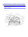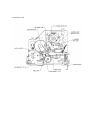
1
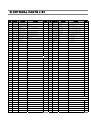
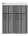
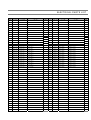
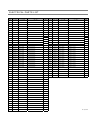
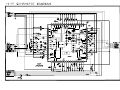
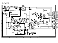
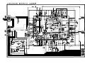
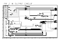
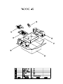
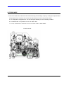
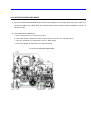
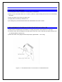
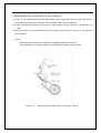
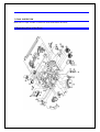
Service Manual
MOBILE CAR VCR
Rev. Jan29,2002A.
SPECIFICATIONS
SYSTEM
Video Signal
VIDEO
Input
Output
Recording system
Signal to Noise ratio
Horizontal Resolution
AUDIO
Input
Output
Frequency Response
Signal to Noise Ratio
Audio Distortion
TAPE TRANSPORT
Format
Tape Width
Tape Speed
FF/REW Time
GENERAL
Power Requirements
Power Consumption
Operating Temperature
DIMENSIONS
Carton size (W*H*D)
Set size (W*H*D)
Weight
NTSC-M
1.0Vpp, 75 ohms, unbalanced
1.0Vpp, 75 ohms, unbalanced
Rotary two-head helical scan
More than 43dB (for NTSC-SP)
More than 41dB (for NTSC-EP)
220 Lines (for NTSC-SP)
210 Lines (for NTSC-SP)
-8.8dBm, 47k ohms Minimum
-5.8dBm ± 2 dBm(1kHz), 1k ohms Maximum
20Hz ~ 20kHz(for PAL Hi Fi SP/EP)
68dB Minimum (SP/EP, Hi Fi)
42dB Minimum (SP, Mono)
0.7% Maximum (SP/EP, Hi Fi)
4.0% Maximum (SP, Mono)
VHS standard
12.65mm (1/2 inch)
SP : 33.35mm/s (for NTSC)
EP : 11.12mm/s (for NTSC)
About 4 Min.(T-120)
DC12V
13W
5°C ~ 35°C (Humidity : 80% Maximum, Operating)
-20°C ~ 60°C (Storage)
300 * 150 * 300 mm
265 * 91 * 275 mm
Approx. 3.0Kg(NET)
Rev. Jan29,2002A.
ELECTRICAL ADJUSTMENT
1. SERVO/SYSCON CIRCUIT ADJUSTMENT METHOD
◆ VIDEO HEAD SWITCHING POSITION
Item
REC Knob
Checking Point
CH.1:PT01 Pin4
CH.2:A/V Video Out
◆ CONNECTION METHOD
Measuring Equipment
Mode
Test Tape
OSCILLOSCOPE
PB
SN-1
VIDEO OUT
CH-1
Oscilloscope
CH-2
PT01 No.4
◆ ADJUSTMENT PROCEDURE
1) Play back the test tape.
2) Set the oscilloscope in the chop mode connect th CH1 to SW pulse(PT01 (4) PIN), the CH2 to
AV1(video out) with CH1 triggering.
3) Press REC Knob to position the V-Sync at 6.5 ± 0.5H from the rising edge of sw pulse.
◆ Adjustment Inspection Standard : 6.5 ± 0.5H
CH1
Vertical SYNC Signal
SW PULSE
(PT01[4]PIN)
CH2
VIDEO OUT
(AV1)
1H
Trigger Position
0.5H
6.5H 0.5H
ELECTRICAL PARTS LIST
LOC
PART-CODE
PART-NAME
PART-DESC
-
REMARK
LOC
C812
PART-CODE
PART-NAME
CEXE1V331A C ELECTRO
PART-DESC
1
486SA01100 ACCESSORY AS
D001
97P0424100 COVER ACCESSORY LD-PE T0.1
DD501
D002
486A716202 BATTERY
AAA 1.5V(SUPERGARD)
DL508
DSRM5670A- LED LAMP
SRM5670-A,2COLOR(RED,GRN)
D003
935S001200 MANUAL OWNERS
-
DL509
DSRM5670A- LED LAMP
SRM5670-A,2COLOR(RED,GRN)
DS1R481T-- LED IR
35V RS 330MF (12.5X18) TP
SIR-481T(P-RANK)
D004
125S000900 CABLE CONN AS
3H-3S TRIP 550MM FUSE
DL510
DSRM5670A- LED LAMP
SRM5670-A,2COLOR(RED,GRN)
D004A
5FSCB2022S FUSE GLASS TUBE
SEMKO T2AH 250V MF51
DL511
DSRM5670A- LED LAMP
SRM5670-A,2COLOR(RED,GRN)
D005
97P881UB50 CABLE R.S AS
ST PLUG-RMC REV 5.0M
DL501
DSM5411H-- LED
SM-5411H (GREEN)
D005A
1TS0P1238- IC UNIT R/RECEIVER TSOP1238---
DL502
DSR5411H-- LED
SR-5411H (RED)
D007
561S000500 CONN AS
2P-2P 50MM DC JACK OPTIONAL
DL503
DSR5411H-- LED
SR-5411H (RED)
D008
221SA02200 COVER SCREW AS
-
DL504
DSR5411H-- LED
SR-5411H (RED)
D008A
221S002200 COVER SCREW
LD-PE T0.05, 지퍼락, 50*60
DL505
DSR5411H-- LED
SR-5411H (RED)
D008B
7173400612 SCREW TAPPTITE
TT3 BIN 4*6 BK
DL506
DSM5411H-- LED
SM-5411H (GREEN)
D008C
353S001300 SCREW TAPPING
TYPE-1, TRUSS HEAD 4*16BK
DL507
DSM5411H-- LED
SM-5411H (GREEN)
2
281SA01000 PACKING AS
-
DD501A
97S2302200 HOLDER LED
ABS
C001
11933625--
PAD F/B
EPS (VPDD)
D501A
324S002100 HOLDER LED F
ABS
C002
97P4808500 POLY BAG FOR SET
800*800*T0.5
D804
DSB360----
SB360(3A, 60V) 17.5MM F FORMING
C003
285S002100 BOX CARTON
SW, EX300*SCP150*EX300
H501
1TS0P2238W IC UNIT R/RECEIVER TS0P2238WE1
C004
285S002300 BOX OUT CARTON
DW,황색 A-1 EX 175*K180*K180*EX175
IC502
14ATM24C04 IC EPROM
ATM24C04-10PA-5.0C
3
311SA00900 CHASSIS MAIN AS
-
IC503
1KA3082B-- IC DRIVER
KA3082B
DIODE SCHOTTKY
A001
313S001100 CHASSIS MAIN
HI-PS (VO)
IC802
1KA34063A- DC/DC CONVERTER
KA34063A
A002
243S004100 LABEL SPEC
PE FILM
IC803
1KA34063A- DC/DC CONVERTER
KA34063A
A003
47P4502201 LABEL SERIAL A
ART PAPER 2EA
AV1
97P6315800 JACK PIN
DPAE-9641
A040
221S001800 COVER TOP
SECC T0.5
AV2
97P6317400 JACK PIN
DPAS-9967
A041
7173401212 SCREW TAPTITE
TT2 BIN 4X12 BK
FJ2
97P6310800 JACK DC
YSC-1535
A050
221S001900 COVER BOTTOM
SECC T0.4_각인유
FJ3
974S000002 JACK PHONE
DHAE-9415(EX-REMOCON, BLACK)
A051
7173401211 SCREW TAPTITE
TT2 BIN 4X12 MFZN
FJ1
97P62A0144 CONN WAFER
770968-1,4PIN,DUAL
D100
597SA00600 REMOCON HANDSET -
PJ201
97P8811614 CONN AS
6H-6S 140MM SHIELD
D200
321SA00600 BRKT MOUNT AS
-
PJ202
97P8851210 CONN AS (Y51210)
2H-2S 100MM
D200A
321S000600 BRKT MOUNT
SECC T1.0 + PANT (BK)
PT01
97P6269000 CONN WAFER
00-8283-0612-00000
D200B
221S002100 COVER MOUNT
LD-PE T0.3(150*200)지퍼락
P401
97P62G06D7 CONN HOUSING
GF120 FPC 1.25MM 7P
M01
258SA01500 PANEL FRONT AS
-
P501
97P62T1528 CONN B/B
TMC-JP-A1 PLUG 2.0MM 8P
M021
7173401211 SCREW TAPTITE
TT2 BIN 4X12 MFZN
P502
97P62G06D5 CONN HOUSING
GF120R FPC 1.25MM 5P
M100A
97P4219200 CUSHION PCB
EVA(BLK) (15*7*3T)
P506
97P62T13B2 CONN B/B
TMC-A,SOCKET,2.0MM,2P
M1000
97PC1201D- DECK TOTAL AS
S12-M(NT 2HD HI SP/EP NON DLC)
P504
97P62T12A5 CONN B/B
TAS-X,RECEP2.5MM,5P
P502A
97P88F0514 CABLE FFC
1.25K 5P 140MM(DRUM M/T)
P503
97P6268600 CONN WAFER
00-8283-0212-00000
P503A
97P0S02000 SENSOR DEW
HDP-05-A8
RF101
973S000002 TUNER RF
TADC-H302F
P503B
7003300611 SCREW MACHINE
BIN 3X6 MFZN
R541
RS02F100JS R METAL OXIDE
2W 10 OHM J SMALL F FORMING
Z001
511S000007 PCB MAIN MANUAL A-
R805
RW01B020K- R WIRE WOUND
1W 0.2 OHM K BULK 5MM B FORMING
BA01
97PB250900 CASE PREAMP AS
ET T0.4+SUS304
R810
RW01B020K- R WIRE WOUND
1W 0.2 OHM K BULK 5MM B FORMING
B001
235S001000 BOARD ANT
HI-PS (VO)
S506
97P0S01900 SENSOR REEL
SG-258S
B001A
256S002700 PLATE BOARD
PVC T 0.5
S507
97P0S01900 SENSOR REEL
SG-258S
7175301012 SCREW TAPPTITE
B0011
TT2 FLT 3X10 MFZN BLACK
S502
TST5811---
C801
CEXF1E681F C ELECTRO
25V RX 680MF 10X20
S502A
97P2342101 HOLDER P/T
TR PHOTO
ABS(HF-06601)
C808
CEXF1E681F C ELECTRO
25V RX 680MF 10X20
S503
TST5811---
ST-5811(D-RANK)
C810
CEXF1E681F C ELECTRO
25V RX 680MF 10X20
S503A
97P2342101 HOLDER P/T
TR PHOTO
ST-5811(D-RANK)
ABS(HF-06601)
REMARK
LOC
PART-CODE
PART-NAME
PART-DESC
REMARK
LOC
PART-CODE
PART-NAME
PART-DESC
S505
5SN0101Z20 SW DETECT
JDS1105-6X
C403
HCBK104KCA C CHIP CERA
50V X7R 0.1MF K 2012
S504
972S000001 SENSOR THERMAL
10K OHM(LNTK103HW)
C409
HCBK473KCA C CHIP CERA
50V X7R 0.047MF K 2012
L802
56C351K---
COIL CHOKE
350UH K EI1614
C410
HCQK510JCA C CHIP CERA
50V CH 51PF J 2012
L803
56C351K---
COIL CHOKE
350UH K EI1614
C412
HCBK223KCA C CHIP CERA
50V X7R 0.022MF K 2012
X602
5XJ14R31AE CRYSTAL QUARTZ
HC-49/S 14.31818MHZ 30PPM CL=16PF
C413
HCBK223KCA C CHIP CERA
50V X7R 0.022MF K 2012
0I801
960S000001 RADIATOR SUB AS
NTD3000PD(0100+78R12)
C415
HCBK103KCA C CHIP CERA
50V X7R 0.01MF K 2012
IC801
1KA78R12-- IC REGULATOR
KA78R12
C418
HCBK104KCA C CHIP CERA
50V X7R 0.1MF K 2012
I801A
NE1MP00100 RADIATOR TR
AL UL/CSA(NCL3300)
C420
HCBK104KCA C CHIP CERA
50V X7R 0.1MF K 2012
I801B
7174300811 SCREW TAPPTITE
TT2 RND 3X8 MFZN
C421
HCBK103KCA C CHIP CERA
50V X7R 0.01MF K 2012
I801C
2291130215 GREASE SILICON
G-600
C422
HCBK103KCA C CHIP CERA
50V X7R 0.01MF K 2012
0Q803
960S000002 RADIATOR SUB AS
NTD3000PD(0100+A1010)
C425
HCBK103KCA C CHIP CERA
50V X7R 0.01MF K 2012
Q803
1KSA1010Y- TR
KSA1010Y
C426
HCBK103KCA C CHIP CERA
50V X7R 0.01MF K 2012
Q803A
NE1MP00100 RADIATOR TR
AL UL/CSA(NCL3300)
C430
HCBK104KCA C CHIP CERA
50V X7R 0.1MF K 2012
7174300811 SCREW TAPPTITE
TT2 RND 3X8 MFZN
C432
HCBK104KCA C CHIP CERA
50V X7R 0.1MF K 2012
Q803C
2291130215 GREASE SILICON
G-600
C438
HCBK103KCA C CHIP CERA
50V X7R 0.01MF K 2012
11
512S000011 PCB MAIN CHIP AS
CHIP
C448
HCBK103KCA C CHIP CERA
50V X7R 0.01MF K 2012
Q803B
F1SS01A
UL/CSA/TUV 1.10A SMD1812P110TS/16
C453
HCBK103KCA C CHIP CERA
50V X7R 0.01MF K 2012
C109
HCBK104KCA C CHIP CERA
5F1JA1124- FUSE PTC
50V X7R 0.1MF K 2012
C456
HCQK201JCA C CHIP CERA
50V CH 200PF J 2012
C110
HCLK560JCA C CHIP CERA
50V SL 56PF J 2012
C457
HCQK390JCA C CHIP CERA
50V CH 39PF J 2012
C111
HCLK560JCA C CHIP CERA
50V SL 56PF J 2012
C459
HCQK391JCA C CHIP CERA
50V CH 390PF J 2012
C113
HCBK123KCA C CHIP CERA
50V X7R 0.012MF K 2012
C460
HCQK509CCA C CHIP CERA
50V CH 5PF C 2012
C114
HCBK123KCA C CHIP CERA
50V X7R 0.012MF K 2012
C462
HCQK270JCA C CHIP CERA
50V CH 27PF J 2012
C116
HCBK103KCA C CHIP CERA
50V X7R 0.01MF K 2012
C463
HCBK103KCA C CHIP CERA
50V X7R 0.01MF K 2012
C204
HCBK103KCA C CHIP CERA
50V X7R 0.01MF K 2012
C467
HCBK473KCA C CHIP CERA
50V X7R 0.047MF K 2012
C206
HCBK472KCA C CHIP CERA
50V X7R 4700PF K 2012
C472
HCBK104KCA C CHIP CERA
50V X7R 0.1MF K 2012
C207
HCBK332KCA C CHIP CERA
50V X7R 3300PF K 2012
C473
HCBK104KCA C CHIP CERA
50V X7R 0.1MF K 2012
C209
HCBK104KCA C CHIP CERA
50V X7R 0.1MF K 2012
C477
HCBK104KCA C CHIP CERA
50V X7R 0.1MF K 2012
C210
HCBK332KCA C CHIP CERA
50V X7R 3300PF K 2012
C501
HCBK223KCA C CHIP CERA
50V X7R 0.022MF K 2012
C211
HCLK561JCA C CHIP CERA
50V SL 560PF J 2012
C502
HCBK104KCA C CHIP CERA
50V X7R 0.1MF K 2012
C213
HCBK102KCA C CHIP CERA
50V X7R 1000PF K 2012
C503
HCBK104KCA C CHIP CERA
50V X7R 0.1MF K 2012
C215
HCBK332KCA C CHIP CERA
50V X7R 3300PF K 2012
C504
HCBK103KCA C CHIP CERA
50V X7R 0.01MF K 2012
C216
HCBK472KCA C CHIP CERA
50V X7R 4700PF K 2012
C505
HCBK103KCA C CHIP CERA
50V X7R 0.01MF K 2012
C217
HCBK104KCA C CHIP CERA
50V X7R 0.1MF K 2012
C506
HCBK103KCA C CHIP CERA
50V X7R 0.01MF K 2012
C220
HCBK103KCA C CHIP CERA
50V X7R 0.01MF K 2012
C507
HCBK104KCA C CHIP CERA
50V X7R 0.1MF K 2012
C224
HCBK102KCA C CHIP CERA
50V X7R 1000PF K 2012
C508
HCBK103KCA C CHIP CERA
50V X7R 0.01MF K 2012
C226
HCBK103KCA C CHIP CERA
50V X7R 0.01MF K 2012
C509
HCBK103KCA C CHIP CERA
50V X7R 0.01MF K 2012
C228
HCLK392KCA C CHIP CERA
50V SL 3900PF K 2012
C510
HCBK104KCA C CHIP CERA
50V X7R 0.1MF K 2012
C232
HCLK392KCA C CHIP CERA
50V SL 3900PF K 2012
C511
HCQK200JCA C CHIP CERA
50V CH 20PF J 2012
C233
HCBK182KCA C CHIP CERA
50V X7R 1800PF K 2012
C512
HCQK180JCA C CHIP CERA
50V CH 18PF J 2012
C234
HCBK104KCA C CHIP CERA
50V X7R 0.1MF K 2012
C513
HCQK180JCA C CHIP CERA
50V CH 18PF J 2012
C241
HCQK821JCA C CHIP CERA
50V CH 820PF J 2012
C514
HCQK180JCA C CHIP CERA
50V CH 18PF J 2012
C242
HCBK332KCA C CHIP CERA
50V X7R 3300PF K 2012
C515
HCBK103KCA C CHIP CERA
50V X7R 0.01MF K 2012
C245
HCBK152KCA C CHIP CERA
50V X7R 1500PF K 2012
C516
HCQK471JCA C CHIP CERA
50V CH 470PF J 2012
C247
HCBK104KCA C CHIP CERA
50V X7R 0.1MF K 2012
C517
HCBK104KCA C CHIP CERA
50V X7R 0.1MF K 2012
C248
HCBK104KCA C CHIP CERA
50V X7R 0.1MF K 2012
C519
HCBK562KCA C CHIP CERA
50V X7R 5600PF K 2012
C252
HCLK391JCA C CHIP CERA
50V SL 390PF J 2012
C521
HCBK104KCA C CHIP CERA
50V X7R 0.1MF K 2012
REMARK
ELECTRICAL PARTS LIST
LOC
PART-CODE
PART-NAME
PART-DESC
REMARK
LOC
PART-CODE
PART-NAME
PART-DESC
C522
HCBK104KCA C CHIP CERA
50V X7R 0.1MF K 2012
JW022
HRF8000-EA R CHIP
1/8 0 OHM 3216
C523
HCBK103KCA C CHIP CERA
50V X7R 0.01MF K 2012
JW023
HRF8000-EA R CHIP
1/8 0 OHM 3216
C524
HCBK103KCA C CHIP CERA
50V X7R 0.01MF K 2012
JW024
HRF8000-EA R CHIP
1/8 0 OHM 3216
C526
HCBK103KCA C CHIP CERA
50V X7R 0.01MF K 2012
JW025
HRF8000-EA R CHIP
1/8 0 OHM 3216
C527
HCBK102KCA C CHIP CERA
50V X7R 1000PF K 2012
JW026
HRF8000-EA R CHIP
1/8 0 OHM 3216
C528
HCBK102KCA C CHIP CERA
50V X7R 1000PF K 2012
JW027
HRF8000-EA R CHIP
1/8 0 OHM 3216
C529
HCBK223KCA C CHIP CERA
50V X7R 0.022MF K 2012
JW028
HRF8000-EA R CHIP
1/8 0 OHM 3216
C530
HCBK104KCA C CHIP CERA
50V X7R 0.1MF K 2012
JW029
HRF8000-EA R CHIP
1/8 0 OHM 3216
C531
HCBK104KCA C CHIP CERA
50V X7R 0.1MF K 2012
JW030
HRF8000-EA R CHIP
1/8 0 OHM 3216
C532
HCBK102KCA C CHIP CERA
50V X7R 1000PF K 2012
JW031
HRF8000-EA R CHIP
1/8 0 OHM 3216
C533
HCBK222KCA C CHIP CERA
50V X7R 2200PF K 2012
JW032
HRF8000-EA R CHIP
1/8 0 OHM 3216
C535
HCBK103KCA C CHIP CERA
50V X7R 0.01MF K 2012
JW033
HRF8000-EA R CHIP
1/8 0 OHM 3216
C538
HCBK103KCA C CHIP CERA
50V X7R 0.01MF K 2012
JW034
HRF8000-EA R CHIP
1/8 0 OHM 3216
C540
HCBK121JCA C CHIP CERA
50V X7R 120PF J 2012
JW035
HRF8000-EA R CHIP
1/8 0 OHM 3216
C544
HCBK104KCA C CHIP CERA
50V X7R 0.1MF K 2012
JW036
HRF8000-EA R CHIP
1/8 0 OHM 3216
C803
HCBK104KCA C CHIP CERA
50V X7R 0.1MF K 2012
JW037
HRF8000-EA R CHIP
1/8 0 OHM 3216
C804
HCBK104KCA C CHIP CERA
50V X7R 0.1MF K 2012
JW038
HRF8000-EA R CHIP
1/8 0 OHM 3216
C805
HCBK103KCA C CHIP CERA
50V X7R 0.01MF K 2012
JW039
HRF8000-EA R CHIP
1/8 0 OHM 3216
C807
HCBK103KCA C CHIP CERA
50V X7R 0.01MF K 2012
Q809(E-C HRFT000-CA R CHIP
1/10 0 OHM 2012
C809
HCQK101JCA C CHIP CERA
50V CH 100PF J 2012
OPT(O)
1/10 1K OHM J 2012
HRFT102JCA R CHIP
C813
HCBK104KCA C CHIP CERA
50V X7R 0.1MF K 2012
Q501
TKSR1104-B TR CHIP
KSR1104
C817
HCBK104KCA C CHIP CERA
50V X7R 0.1MF K 2012
Q502
TKSR1104-B TR CHIP
KSR1104
C818
HCQK201JCA C CHIP CERA
50V CH 200PF J 2012
Q503
TKSR1104-B TR CHIP
KSR1104
C820
HCBK104KCA C CHIP CERA
50V X7R 0.1MF K 2012
Q504
TKSR1104-B TR CHIP
KSR1104
C821
HCBK104KCA C CHIP CERA
50V X7R 0.1MF K 2012
Q505
TKSR1104-B TR CHIP
KSR1104
C900
HCBK104KCA C CHIP CERA
50V X7R 0.1MF K 2012
Q506
TKSR1104-B TR CHIP
KSR1104
CQ803
HCQK471JCA C CHIP CERA
50V CH 470PF J 2012
Q507
TKSR1104-B TR CHIP
KSR1104
IC201
1LA72637M- IC HI-FI
LA72637M
Q508
TKSR1104-B TR CHIP
KSR1104
IC401
1LA71578-- IC AV
LA71578
Q509
T2SC2412KB TR CHIP
2SC2412K-T146-BR
IC501
1M37760133 IC MICOM
M37760M8H-133GP
Q510
TKSR1104-B TR CHIP
KSR1104
JW001
HRF8000-EA R CHIP
1/8 0 OHM 3216
Q512
TKSR1104-B TR CHIP
KSR1104
JW002
HRF8000-EA R CHIP
1/8 0 OHM 3216
R101
HRFT470JCA R CHIP
1/10 47 OHM J 2012
JW003
HRF8000-EA R CHIP
1/8 0 OHM 3216
R103
HRFT750JCA R CHIP
1/10 75 OHM J 2012
JW004
HRF8000-EA R CHIP
1/8 0 OHM 3216
R106
HRFT750JCA R CHIP
1/10 75 OHM J 2012
JW005
HRF8000-EA R CHIP
1/8 0 OHM 3216
R109
HRFT303JCA R CHIP
1/10 30K OHM J 2012
JW008
HRF8000-EA R CHIP
1/8 0 OHM 3216
R111
HRFT122JCA R CHIP
1/10 1.2K OHM J 2012
JW009
HRF8000-EA R CHIP
1/8 0 OHM 3216
R112
HRFT222JCA R CHIP
1/10 2.2K OHM J 2012
JW010
HRF8000-EA R CHIP
1/8 0 OHM 3216
R113
HRFT122JCA R CHIP
1/10 1.2K OHM J 2012
JW011
HRF8000-EA R CHIP
1/8 0 OHM 3216
R120
HRFT103JCA R CHIP
1/10 10K OHM J 2012
JW012
HRF8000-EA R CHIP
1/8 0 OHM 3216
R121
HRFT750JCA R CHIP
1/10 75 OHM J 2012
JW013
HRF8000-EA R CHIP
1/8 0 OHM 3216
R125
HRFT102JCA R CHIP
1/10 1K OHM J 2012
JW016
HRF8000-EA R CHIP
1/8 0 OHM 3216
R202
HRFT563JCA R CHIP
1/10 56K OHM J 2012
JW017
HRF8000-EA R CHIP
1/8 0 OHM 3216
R205
HRFT564JCA R CHIP
1/10 560K OHM J 2012
JW018
HRF8000-EA R CHIP
1/8 0 OHM 3216
R206
HRFT202JCA R CHIP
1/10 2K OHM J 2012
JW019
HRF8000-EA R CHIP
1/8 0 OHM 3216
R207
HRFT331JCA R CHIP
1/10 330 OHM J 2012
JW020
HRF8000-EA R CHIP
1/8 0 OHM 3216
R208
HRFT563JCA R CHIP
1/10 56K OHM J 2012
REMARK
ELECTRICAL PARTS LIST
LOC
PART-CODE
PART-NAME
PART-DESC
REMARK
LOC
PART-CODE
PART-NAME
PART-DESC
R210
HRFT183JCA R CHIP
1/10 18K OHM J 2012
R440
HRFT152JCA R CHIP
1/10 1.5K OHM J 2012
R215
HRFT203JCA R CHIP
1/10 20K OHM J 2012
R451
HRFT393JCA R CHIP
1/10 39K OHM J 2012
R216
HRFT103JCA R CHIP
1/10 10K OHM J 2012
R501
HRFT123JCA R CHIP
1/10 12K OHM J 2012
R217
HRFT623JCA R CHIP
1/10 62K OHM J 2012
R502
HRFT332JCA R CHIP
1/10 3.3K OHM J 2012
R218
HRFT183JCA R CHIP
1/10 18K OHM J 2012
R503
HRFT153JCA R CHIP
1/10 15K OHM J 2012
R223
HRFT183JCA R CHIP
1/10 18K OHM J 2012
R504
HRFT473JCA R CHIP
1/10 47K OHM J 2012
R241
HRFT911GCA R CHIP
1/10 910 OHM G
R507
HRFT474JCA R CHIP
1/10 470K OHM J 2012
R242
HRFT273JCA R CHIP
1/10 27K OHM J 2012
R508
HRFT334JCA R CHIP
1/10 330K OHM J 2012
R243
HRFT201JCA R CHIP
1/10 200 OHM J 2012
R509
HRFT123JCA R CHIP
1/10 12K OHM J 2012
R244
HRFT334JCA R CHIP
1/10 330K OHM J 2012
R510
HRFT274JCA R CHIP
1/10 270K OHM J 2012
R245
HRFT123JCA R CHIP
1/10 12K OHM J 2012
R512
HRFT473JCA R CHIP
1/10 47K OHM J 2012
R246
HRFT822JCA R CHIP
1/10 8.2K OHM J 2012
R513
HRFT682JCA R CHIP
1/10 6.8K OHM J 2012
R247
HRFT822JCA R CHIP
1/10 8.2K OHM J 2012
R515
HRFT474JCA R CHIP
1/10 470K OHM J 2012
R249
HRFT272JCA R CHIP
1/10 2.7K OHM J 2012
R516
HRFT153JCA R CHIP
1/10 15K OHM J 2012
R251
HRFT472JCA R CHIP
1/10 4.7K OHM J 2012
R517
HRFT103JCA R CHIP
1/10 10K OHM J 2012
R253
HRFT562JCA R CHIP
1/10 5.6K OHM J 2012
R519
HRFT103JCA R CHIP
1/10 10K OHM J 2012
R254
HRFT123JCA R CHIP
1/10 12K OHM J 2012
R522
HRFT132JCA R CHIP
1/10 1.3K OHM J 2012
R256
HRFT000-CA
1/10 0 OHM 2012
R523
HRFT102JCA R CHIP
1/10 1K OHM J 2012
R CHIP
R257
HRFT223JCA R CHIP
1/10 22K OHM J 2012
R524
HRFT822JCA R CHIP
1/10 8.2K OHM J 2012
R258
HRFT622JCA R CHIP
1/10 6.2K OHM J 2012
R525
HRFT153JCA R CHIP
1/10 15K OHM J 2012
R259
HRFT181GCA R CHIP
1/10 180 OHM G 2012
R532
HRFT222JCA R CHIP
1/10 2.2K OHM J 2012
R260
HRFT222JCA R CHIP
1/10 2.2K OHM J 2012
R534
HRFT472JCA R CHIP
1/10 4.7K OHM J 2012
R261
HRFT103JCA R CHIP
1/10 10K OHM J 2012
R535
HRFT472JCA R CHIP
1/10 4.7K OHM J 2012
R262
HRFT223JCA R CHIP
1/10 22K OHM J 2012
R536
HRFT103JCA R CHIP
1/10 10K OHM J 2012
R263
HRFT512JCA R CHIP
1/10 5.1K OHM J 2012
R537
HRFT473JCA R CHIP
1/10 47K OHM J 2012
R264
HRFT103JCA R CHIP
1/10 10K OHM J 2012
R538
HRFT473JCA R CHIP
1/10 47K OHM J 2012
R265
HRFT561JCA R CHIP
1/10 560 OHM J 2012
R546
HRFT473JCA R CHIP
1/10 47K OHM J 2012
R266
HRFT101JCA R CHIP
1/10 100 OHM J 2012
R547
HRFT201JCA R CHIP
1/10 200 OHM J 2012
R267
HRFT103JCA R CHIP
1/10 10K OHM J 2012
R548
HRFT273JCA R CHIP
1/10 27K OHM J 2012
R401
HRFT472JCA R CHIP
1/10 4.7K OHM J 2012
R549
HRFT101JCA R CHIP
1/10 100 OHM J 2012
R402
HRFT273JCA R CHIP
1/10 27K OHM J 2012
R550
HRFT201JCA R CHIP
1/10 200 OHM J 2012
R403
HRFT473JCA R CHIP
1/10 47K OHM J 2012
R551
HRFT273JCA R CHIP
1/10 27K OHM J 2012
R406
HRFT822JCA R CHIP
1/10 8.2K OHM J 2012
R553
HRFT103JCA R CHIP
1/10 10K OHM J 2012
R408
HRFT182JCA R CHIP
1/10 1.8K OHM J 2012
R554
HRFT103JCA R CHIP
1/10 10K OHM J 2012
R410
HRFT102JCA R CHIP
1/10 1K OHM J 2012
R559
HRFT332JCA R CHIP
1/10 3.3K OHM J 2012
R413
HRFT563JCA R CHIP
1/10 56K OHM J 2012
R560
HRFT121JCA R CHIP
1/10 120 OHM J 2012
R416
HRFT513JCA R CHIP
1/10 51K OHM J 2012
R561
HRFT121JCA R CHIP
1/10 120 OHM J 2012
R420
HRFT472JCA R CHIP
1/10 4.7K OHM J 2012
R568
HRFT331JCA R CHIP
1/10 330 OHM J 2012
R421
HRFT561JCA R CHIP
1/10 560 OHM J 2012
R573
HRFT331JCA R CHIP
1/10 330 OHM J 2012
R423
HRFT272JCA R CHIP
1/10 2.7K OHM J 2012
R581
HRFT331JCA R CHIP
1/10 330 OHM J 2012
R424
HRFT201JCA R CHIP
1/10 200 OHM J 2012
R583
HRFT472JCA R CHIP
1/10 4.7K OHM J 2012
R425
HRFT331JCA R CHIP
1/10 330 OHM J 2012
R585
HRFT473JCA R CHIP
1/10 47K OHM J 2012
R426
HRFT122JCA R CHIP
1/10 1.2K OHM J 2012
R587
HRFT473JCA R CHIP
1/10 47K OHM J 2012
R427
HRFT331JCA R CHIP
1/10 330 OHM J 2012
R589
HRFT473JCA R CHIP
1/10 47K OHM J 2012
R432
HRFT123JCA R CHIP
1/10 12K OHM J 2012
R590
HRFT102JCA R CHIP
1/10 1K OHM J 2012
R438
HRFT511JCA R CHIP
1/10 510 OHM J 2012
R591
HRFT102JCA R CHIP
1/10 1K OHM J 2012
REMARK
ELECTRICAL PARTS LIST
LOC
PART-CODE
PART-NAME
PART-DESC
REMARK
LOC
PART-CODE
PART-NAME
PART-DESC
R592
HRFT473JCA R CHIP
1/10 47K OHM J 2012
C419
CEXF1C101A C ELECTRO
16V RSM 100MF (6.3X7) TP
R801
HRFT123JCA R CHIP
1/10 12K OHM J 2012
C427
CEXF1H109A C ELECTRO
50V RSM 1MF (4X7) TP
R806
HRFT122JCA R CHIP
1/10 1.2K OHM J 2012
C428
CEXF1H100A C ELECTRO
50V RSM 10MF (5X7) TP
R808
HRFT822JCA R CHIP
1/10 8.2K OHM J 2012
C429
CEXF1H109A C ELECTRO
50V RSM 1MF (4X7) TP
R809
HRFT222JCA R CHIP
1/10 2.2K OHM J 2012
C431
CEXF1C470A C ELECTRO
16V RSM 47MF (5X7) TP
R812
HRFT163JCA R CHIP
1/10 16K OHM J 2012
C433
CEXF1C470A C ELECTRO
16V RSM 47MF (5X7) TP
R813
HRFT151JCA R CHIP
1/10 150 OHM J 2012
C437
CEXF1H109A C ELECTRO
50V RSM 1MF (4X7) TP
C451
CEXF1H100A C ELECTRO
50V RSM 10MF (5X7) TP
12
512S000012 PCB MAIN RADIAL AS-
C107
CEXF1H100A C ELECTRO
50V RSM 10MF (5X7) TP
C452
CEXF1H100A C ELECTRO
50V RSM 10MF (5X7) TP
C108
CEXE0J221S C ELECTRO
6.3V RSA 220MF 6.3X7
C458
CEXF1H339A C ELECTRO
50V RSM 3.3MF 4X7
C118
CEXF1C471V C ELECTRO
16V RSS 470MF 8X11.5 TP
C464
CEXE0J221S C ELECTRO
6.3V RSA 220MF 6.3X7
C119
CEXF1C471V C ELECTRO
16V RSS 470MF 8X11.5 TP
C466
CEXF1H109A C ELECTRO
50V RSM 1MF (4X7) TP
C121
CEXF1C470A C ELECTRO
16V RSM 47MF (5X7) TP
C475
CEXF1C470A C ELECTRO
16V RSM 47MF (5X7) TP
C122
CEXF1C470A C ELECTRO
16V RSM 47MF (5X7) TP
C476
CEXF1C220A C ELECTRO
16V RSM 22MF (5X7)
C201
CEXF1H109A C ELECTRO
50V RSM 1MF (4X7) TP
C478
CEXF1C220A C ELECTRO
16V RSM 22MF (5X7)
C202
CEXF1C100A C ELECTRO
16V RSM 10MF 4X7
C518
CEXF1H109A C ELECTRO
50V RSM 1MF (4X7) TP
C203
CEXF1H479A C ELECTRO
50V RSM 4.7MF (4X7) TP
C534
CEXF1C470A C ELECTRO
16V RSM 47MF (5X7) TP
C205
CEXF1C220A C ELECTRO
16V RSM 22MF (5X7)
C537
CEXF1C101A C ELECTRO
16V RSM 100MF (6.3X7) TP
C208
CEXF1H108A C ELECTRO
50V RSM 0.1MF 4X7
C541
CEXF1C470A C ELECTRO
16V RSM 47MF (5X7) TP
C212
CEXF1H479A C ELECTRO
50V RSM 4.7MF (4X7) TP
C550
CEXF1C100A C ELECTRO
16V RSM 10MF 4X7
C214
CEXE0J221S C ELECTRO
6.3V RSA 220MF 6.3X7
C551
CEXF1C100A C ELECTRO
16V RSM 10MF 4X7
C218
CEXF1E220A C ELECTRO
25V RSM 22MF 6.3X7 TP
C552
CEXF1C470A C ELECTRO
16V RSM 47MF (5X7) TP
C219
CEXF1E220A C ELECTRO
25V RSM 22MF 6.3X7 TP
C553
CEXF1C101A C ELECTRO
16V RSM 100MF (6.3X7) TP
C221
CEXF1H479A C ELECTRO
50V RSM 4.7MF (4X7) TP
C554
CEXF1C100A C ELECTRO
16V RSM 10MF 4X7
C222
CEXF1C100A C ELECTRO
16V RSM 10MF 4X7
C802
CEXF1C221V C ELECTRO
16V RSS 220MF (8X11.5) TP
C223
CEXF1H109A C ELECTRO
50V RSM 1MF (4X7) TP
C811
CEXF1H479A C ELECTRO
50V RSM 4.7MF (4X7) TP
C225
CEXF1H100A C ELECTRO
50V RSM 10MF (5X7) TP
C814
CEXF1C101A C ELECTRO
16V RSM 100MF (6.3X7) TP
C227
CEXF1C101A C ELECTRO
16V RSM 100MF (6.3X7) TP
C815
CEXF1C101A C ELECTRO
16V RSM 100MF (6.3X7) TP
C229
CEXF1C100A C ELECTRO
16V RSM 10MF 4X7
C816
CEXF1C101A C ELECTRO
16V RSM 100MF (6.3X7) TP
CEXF1C101A C ELECTRO
C231
CEXF1C100A C ELECTRO
16V RSM 10MF 4X7
C819
C243
CEXF1H100A C ELECTRO
50V RSM 10MF (5X7) TP
IC504
C244
CMXM2A103J C MYLAR
100V 0.01MF J (TP)
IC804
1K1A78L05- IC REGULATOR
KIA78L05 (RADIAL)
C246
CEXF1H479A C ELECTRO
50V RSM 4.7MF (4X7) TP
L107
5CPX101J2T COIL PEAKING
100UH(BRN-BRN)
C249
CMXV2A153J C MYLAR
100V 0.015MF J (TP) SMALL
L201
5CPX100J2T COIL PEAKING
10UH(BRN-BLK)
C250
CEXF1H479A C ELECTRO
50V RSM 4.7MF (4X7) TP
L241
5CPX680J2T COIL PEAKING
68UH(BLU-BLK)
1K1A7031P- IC SWITCH RESET
16V RSM 100MF (6.3X7) TP
KIA7031P
C251
CEXF1C470A C ELECTRO
16V RSM 47MF (5X7) TP
L401
5CPX100J2T COIL PEAKING
10UH(BRN-BLK)
C253
CMXV2A153J C MYLAR
100V 0.015MF J (TP) SMALL
L402
5CPX100J2T COIL PEAKING
10UH(BRN-BLK)
C255
CEXF1C220A C ELECTRO
16V RSM 22MF (5X7)
L404
5CPX100J2T COIL PEAKING
10UH(BRN-BLK)
C290
CEXF1C100A C ELECTRO
16V RSM 10MF 4X7
L405
5CPX100J2T COIL PEAKING
10UH(BRN-BLK)
C401
CEXF1H109A C ELECTRO
50V RSM 1MF (4X7) TP
L406
5CPX100J2T COIL PEAKING
10UH(BRN-BLK)
C402
CEXF1H109A C ELECTRO
50V RSM 1MF (4X7) TP
L501
5CPX229J-- COIL PEAKING
2.2UH J (RADIAL)
C404
CEXF1C101A C ELECTRO
16V RSM 100MF (6.3X7) TP
L503
5CPX471J-- COIL PEAKING
470UH J (RADIAL)
C411
CEXF1H109A C ELECTRO
50V RSM 1MF (4X7) TP
L801
56C220K686 COIL CHOKE
22UH K
C414
CEXF1H109A C ELECTRO
50V RSM 1MF (4X7) TP
L806
56C220K686 COIL CHOKE
22UH K
C416
CEXF1H109A C ELECTRO
50V RSM 1MF (4X7) TP
Q101
TZTA1266Y- TR
KTA1266Y- (AUTO)(1015Y)
C417
CEXF1C470A C ELECTRO
16V RSM 47MF (5X7) TP
Q102
TZTA1266Y- TR
KTA1266Y- (AUTO)(1015Y)
REMARK
ELECTRICAL PARTS LIST
LOC
PART-CODE
PART-NAME
PART-DESC
REMARK
LOC
Q241
TZTA1266Y- TR
KTA1266Y- (AUTO)(1015Y)
D810
Q242
TZTC3198Y- TR
KTC3198Y-(1815Y) (AUTO)
D811
Q243
TZTC3202Y- TR
KTC3202Y (AUTO)(1959Y)
D812
Q244
TZTA1266Y- TR
KTA1266Y- (AUTO)(1015Y)
D813
PART-CODE
PART-NAME
DZN5819--- DIODE
DZUZ9R1BSC DIODE ZENER
DZN4148--- DIODE
DZMTZJ5R1B DIODE ZENER
PART-DESC
1N5819 40V,1A AUTO
UZ-9.1BSC(8.89-9.29V)
1N4148
MTZ J 5.1B(4.94-5.20)
Q245
TZTC3198Y- TR
KTC3198Y-(1815Y) (AUTO)
D814
DZN4148--- DIODE
1N4148
Q246
TZTC3198Y- TR
KTC3198Y-(1815Y) (AUTO)
L202
5CPZ680K02 COIL PEAKING
68UH K (AXIAL 3.5MM)
Q402
TZTC3198Y- TR
KTC3198Y-(1815Y) (AUTO)
L407
5CPZ560J02 COIL PEAKING
56UH J (AXIAL 3.5MM)
Q403
TZTC3198Y- TR
KTC3198Y-(1815Y) (AUTO)
R110
RD-AZ243J- R CARBON FILM
1/6 24K OHM J
Q407
TZTA1266Y- TR
KTA1266Y- (AUTO)(1015Y)
R114
RD-AZ102J- R CARBON FILM
1/6 1K OHM J
Q801
TZSR1001-- TR
KSR1001 (AUTO)
R115
RD-AZ473J- R CARBON FILM
1/6 47K OHM J
Q802
TZTA1273Y- TR
KTA1273Y(928A)
R119
RD-4Z471J- R CARBON FILM
1/4 470 OHM J
Q804
TZTC3205Y- TR
KTC3205Y (2236Y)
R201
RD-AZ154J- R CARBON FILM
1/6 150K OHM J
Q805
TZTC3205Y- TR
KTC3205Y (2236Y)
R203
RD-AZ152J- R CARBON FILM
1/6 1.5K OHM J
Q806
TZTC3205Y- TR
KTC3205Y (2236Y)
R204
RD-AZ152J- R CARBON FILM
1/6 1.5K OHM J
Q807
TZTC3202Y- TR
KTC3202Y (AUTO)(1959Y)
R209
RD-AZ154J- R CARBON FILM
1/6 150K OHM J
SW501
5S50101Z97 SW TACT
SKHV10914B 9.5M AUTO
R211
RD-AZ623J- R CARBON FILM
1/6 62K OHM J
SW502
5S50101Z97 SW TACT
SKHV10914B 9.5M AUTO
R212
RD-AZ621J- R CARBON FILM
1/6 620 OHM J
SW503
5S50101Z97 SW TACT
SKHV10914B 9.5M AUTO
R213
RD-AZ242J- R CARBON FILM
1/6 2.4K OHM J
SW504
5S50101Z97 SW TACT
SKHV10914B 9.5M AUTO
R214
RD-AZ242J- R CARBON FILM
1/6 2.4K OHM J
SW505
5S50101Z97 SW TACT
SKHV10914B 9.5M AUTO
R219
RD-AZ621J- R CARBON FILM
1/6 620 OHM J
SW506
5S50101Z97 SW TACT
SKHV10914B 9.5M AUTO
R220
RD-AZ183J- R CARBON FILM
1/6 18K OHM J
SW507
5S50101Z97 SW TACT
SKHV10914B 9.5M AUTO
R221
RD-AZ823J- R CARBON FILM
1/6 82K OHM J
HC-49/U 3.579545MHZ 15PPM SER TP
X401
R222
RD-AZ823J- R CARBON FILM
1/6 82K OHM J
13
5XE3R579TB CRYSTAL QUARTZ
512S000013 PCB MAIN AXIAL AS -
R224
RD-AZ102J- R CARBON FILM
1/6 1K OHM J
U001
503S000037 PCB MAIN
247*246*1.6T VER. "B"
R250
RD-AZ123J- R CARBON FILM
1/6 12K OHM J
BD801
5PB13857--
B13857(AXIAL)
R268
RD-AZ102J- R CARBON FILM
1/6 1K OHM J
COIL BEAD
C115
CCZF1H103Z C CERA
50V F 0.01MF Z (TAPPING)
R404
RD-AZ225J- R CARBON FILM
1/6 2.2M OHM J
C424
CCZB1H103K C CERA
HIKB 50V 0.01MF K AXIAL
R407
RD-AZ182J- R CARBON FILM
1/6 1.8K OHM J
C449
CCZF1H104Z C CERA
50V HIKF 0.1MF Z
R411
RD-AZ392J- R CARBON FILM
1/6 3.9K OHM J
C465
CCZF1H104Z C CERA
50V HIKF 0.1MF Z
R414
RD-AZ101J- R CARBON FILM
1/6 100 OHM J
C474
CCZB1H103K C CERA
HIKB 50V 0.01MF K AXIAL
R417
RD-AZ102J- R CARBON FILM
1/6 1K OHM J
C536
CCZB1H103K C CERA
HIKB 50V 0.01MF K AXIAL
R418
RD-AZ152J- R CARBON FILM
1/6 1.5K OHM J
D101
DZN4148--- DIODE
1N4148
R419
RD-AZ152J- R CARBON FILM
1/6 1.5K OHM J
D401
DZN4148--- DIODE
1N4148
R422
RD-AZ561J- R CARBON FILM
1/6 560 OHM J
D402
DZN4148--- DIODE
1N4148
R429
RD-AZ103J- R CARBON FILM
1/6 10K OHM J
D501
DZN4148--- DIODE
1N4148
R430
RD-AZ203J- R CARBON FILM
1/6 20K OHM J
D502
DZN4148--- DIODE
1N4148
R431
RD-AZ203J- R CARBON FILM
1/6 20K OHM J
D503
DZN4148--- DIODE
1N4148
R433
RD-AZ182J- R CARBON FILM
1/6 1.8K OHM J
D504
DZN4148--- DIODE
1N4148
R436
RD-AZ101J- R CARBON FILM
1/6 100 OHM J
DZN4148--- DIODE
1N4148
R437
RD-AZ101J- R CARBON FILM
1/6 100 OHM J
UZ-9.1BSC(8.89-9.29V)
R450
RD-AZ103J- R CARBON FILM
1/6 10K OHM J
D508
D510
DZUZ9R1BSC DIODE ZENER
D512
DZN4002--- DIODE
1N4002
R506
RD-4Z151J- R CARBON FILM
1/4 150 OHM J
D806
DZN4148--- DIODE
1N4148
R511
RD-AZ103J- R CARBON FILM
1/6 10K OHM J
D807
DZN4002--- DIODE
1N4002
R518
RD-AZ103J- R CARBON FILM
1/6 10K OHM J
D808
DZN4148--- DIODE
1N4148
R520
RD-AZ102J- R CARBON FILM
1/6 1K OHM J
D809
DZN5819--- DIODE
1N5819 40V,1A AUTO
R530
RD-AZ221J- R CARBON FILM
1/6 220 OHM J
REMARK
ELECTRICAL PARTS LIST
LOC
PART-CODE
PART-NAME
PART-DESC
REMARK
LOC
PART-CODE
PART-NAME
PART-DESC
R533
RD-AZ122J- R CARBON FILM
1/6 1.2K OHM J
JP012
945S0001--
WIRE COPPER
0.6*43MM TAPING
R539
RD-AZ101J- R CARBON FILM
1/6 100 OHM J
JP013
945S0001--
WIRE COPPER
0.6*43MM TAPING
R540
RD-AZ101J- R CARBON FILM
1/6 100 OHM J
JP014
945S0001--
WIRE COPPER
0.6*43MM TAPING
R543
RD-AZ122J- R CARBON FILM
1/6 1.2K OHM J
JP015
945S0001--
WIRE COPPER
0.6*43MM TAPING
R544
RD-AZ103J- R CARBON FILM
1/6 10K OHM J
JP016
945S0001--
WIRE COPPER
0.6*43MM TAPING
R CARBON FILM
1/6 10K OHM J
JP017
945S0001--
WIRE COPPER
0.6*43MM TAPING
R552
RD-AZ101J- R CARBON FILM
1/6 100 OHM J
JP018
945S0001--
WIRE COPPER
0.6*43MM TAPING
R556
RD-AZ561J- R CARBON FILM
1/6 560 OHM J
JP019
945S0001--
WIRE COPPER
0.6*43MM TAPING
R557
RD-AZ102J- R CARBON FILM
1/6 1K OHM J
JP020
945S0001--
WIRE COPPER
0.6*43MM TAPING
R558
RD-AZ432J- R CARBON FILM
1/6 4.3K OHM J
JP021
945S0001--
WIRE COPPER
0.6*43MM TAPING
R562
RD-AZ331J- R CARBON FILM
1/6 330 OHM J
JP022
945S0001--
WIRE COPPER
0.6*43MM TAPING
R563
RD-AZ331J- R CARBON FILM
1/6 330 OHM J
JP023
945S0001--
WIRE COPPER
0.6*43MM TAPING
R564
RD-AZ331J- R CARBON FILM
1/6 330 OHM J
JP024
945S0001--
WIRE COPPER
0.6*43MM TAPING
R565
RD-AZ331J- R CARBON FILM
1/6 330 OHM J
JP025
945S0001--
WIRE COPPER
0.6*43MM TAPING
R566
RD-AZ102J- R CARBON FILM
1/6 1K OHM J
JP026
945S0001--
WIRE COPPER
0.6*43MM TAPING
R567
RD-AZ331J- R CARBON FILM
1/6 330 OHM J
JP027
945S0001--
WIRE COPPER
0.6*43MM TAPING
R569
RD-AZ331J- R CARBON FILM
1/6 330 OHM J
JP028
945S0001--
WIRE COPPER
0.6*43MM TAPING
R572
RD-AZ331J- R CARBON FILM
1/6 330 OHM J
JP029
945S0001--
WIRE COPPER
0.6*43MM TAPING
R574
RD-AZ331J- R CARBON FILM
1/6 330 OHM J
JP030
945S0001--
WIRE COPPER
0.6*43MM TAPING
R575
RD-AZ331J- R CARBON FILM
1/6 330 OHM J
JP031
945S0001--
WIRE COPPER
0.6*43MM TAPING
R576
RD-AZ331J- R CARBON FILM
1/6 330 OHM J
JP032
945S0001--
WIRE COPPER
0.6*43MM TAPING
R578
RD-AZ331J- R CARBON FILM
1/6 330 OHM J
JP033
945S0001--
WIRE COPPER
0.6*43MM TAPING
R580
RD-AZ331J- R CARBON FILM
1/6 330 OHM J
JP034
945S0001--
WIRE COPPER
0.6*43MM TAPING
R582
RD-AZ472J- R CARBON FILM
1/6 4.7K OHM J
JP035
945S0001--
WIRE COPPER
0.6*43MM TAPING
R584
RD-AZ102J- R CARBON FILM
1/6 1K OHM J
JP036
945S0001--
WIRE COPPER
0.6*43MM TAPING
R586
RD-AZ102J- R CARBON FILM
1/6 1K OHM J
JP037
945S0001--
WIRE COPPER
0.6*43MM TAPING
R588
RD-AZ102J- R CARBON FILM
1/6 1K OHM J
JP038
945S0001--
WIRE COPPER
0.6*43MM TAPING
R545
`
R802
RD-4Z301J- R CARBON FILM
1/4 300 OHM J
JP039
945S0001--
WIRE COPPER
0.6*43MM TAPING
R803
RD-AZ222J- R CARBON FILM
1/6 2.2K OHM J
JP040
945S0001--
WIRE COPPER
0.6*43MM TAPING
R804
RD-AZ122J- R CARBON FILM
1/6 1.2K OHM J
JP041
945S0001--
WIRE COPPER
0.6*43MM TAPING
R807
RD-4Z151J- R CARBON FILM
1/4 150 OHM J
JP042
945S0001--
WIRE COPPER
0.6*43MM TAPING
R811
RD-AZ394J- R CARBON FILM
1/6 390K OHM J
JP043
945S0001--
WIRE COPPER
0.6*43MM TAPING
R814
RD-4Z221J- R CARBON FILM
1/4 220 OHM J
JP044
945S0001--
WIRE COPPER
0.6*43MM TAPING
R815
RD-AZ123J- R CARBON FILM
1/6 12K OHM J
JP045
945S0001--
WIRE COPPER
0.6*43MM TAPING
C539
945S0001--
WIRE COPPER
0.6*43MM TAPING
JP046
945S0001--
WIRE COPPER
0.6*43MM TAPING
C539
945S0001--
WIRE COPPER
0.6*43MM TAPING
JP047
945S0001--
WIRE COPPER
0.6*43MM TAPING
JP002
945S0001--
WIRE COPPER
0.6*43MM TAPING
JP048
945S0001--
WIRE COPPER
0.6*43MM TAPING
JP003
945S0001--
WIRE COPPER
0.6*43MM TAPING
JP049
945S0001--
WIRE COPPER
0.6*43MM TAPING
JP004
945S0001--
WIRE COPPER
0.6*43MM TAPING
JP050
945S0001--
WIRE COPPER
0.6*43MM TAPING
JP005
945S0001--
WIRE COPPER
0.6*43MM TAPING
JP051
945S0001--
WIRE COPPER
0.6*43MM TAPING
JP006
945S0001--
WIRE COPPER
0.6*43MM TAPING
JP052
945S0001--
WIRE COPPER
0.6*43MM TAPING
JP007
945S0001--
WIRE COPPER
0.6*43MM TAPING
JP053
945S0001--
WIRE COPPER
0.6*43MM TAPING
JP008
945S0001--
WIRE COPPER
0.6*43MM TAPING
JP054
945S0001--
WIRE COPPER
0.6*43MM TAPING
JP009
945S0001--
WIRE COPPER
0.6*43MM TAPING
JP055
945S0001--
WIRE COPPER
0.6*43MM TAPING
JP010
945S0001--
WIRE COPPER
0.6*43MM TAPING
JP057
945S0001--
WIRE COPPER
0.6*43MM TAPING
JP011
945S0001--
WIRE COPPER
0.6*43MM TAPING
JP058
945S0001--
WIRE COPPER
0.6*43MM TAPING
REMARK
ELECTRICAL PARTS LIST
LOC
PART-CODE
PART-NAME
PART-DESC
REMARK
LOC
PART-CODE
PART-NAME
PART-DESC
JP059
945S0001--
WIRE COPPER
0.6*43MM TAPING
JP122
945S0001--
WIRE COPPER
0.6*43MM TAPING
JP060
945S0001--
WIRE COPPER
0.6*43MM TAPING
JP123
945S0001--
WIRE COPPER
0.6*43MM TAPING
JP061
945S0001--
WIRE COPPER
0.6*43MM TAPING
JP124
945S0001--
WIRE COPPER
0.6*43MM TAPING
JP062
945S0001--
WIRE COPPER
0.6*43MM TAPING
JP125
945S0001--
WIRE COPPER
0.6*43MM TAPING
JP063
945S0001--
WIRE COPPER
0.6*43MM TAPING
JP126
945S0001--
WIRE COPPER
0.6*43MM TAPING
JP065
945S0001--
WIRE COPPER
0.6*43MM TAPING
JP128
945S0001--
WIRE COPPER
0.6*43MM TAPING
JP067
945S0001--
WIRE COPPER
0.6*43MM TAPING
JP129
945S0001--
WIRE COPPER
0.6*43MM TAPING
JP068
945S0001--
WIRE COPPER
0.6*43MM TAPING
JP133
945S0001--
WIRE COPPER
0.6*43MM TAPING
JP069
945S0001--
WIRE COPPER
0.6*43MM TAPING
JP134
945S0001--
WIRE COPPER
0.6*43MM TAPING
JP070
945S0001--
WIRE COPPER
0.6*43MM TAPING
JP136
945S0001--
WIRE COPPER
0.6*43MM TAPING
JP071
945S0001--
WIRE COPPER
0.6*43MM TAPING
JP137
945S0001--
WIRE COPPER
0.6*43MM TAPING
JP072
945S0001--
WIRE COPPER
0.6*43MM TAPING
JP138
945S0001--
WIRE COPPER
0.6*43MM TAPING
JP073
945S0001--
WIRE COPPER
0.6*43MM TAPING
JP139
945S0001--
WIRE COPPER
0.6*43MM TAPING
JP074
945S0001--
WIRE COPPER
0.6*43MM TAPING
JP140
945S0001--
WIRE COPPER
0.6*43MM TAPING
JP075
945S0001--
WIRE COPPER
0.6*43MM TAPING
JP141
945S0001--
WIRE COPPER
0.6*43MM TAPING
JP077
945S0001--
WIRE COPPER
0.6*43MM TAPING
JP143
945S0001--
WIRE COPPER
0.6*43MM TAPING
JP080
945S0001--
WIRE COPPER
0.6*43MM TAPING
JP144
945S0001--
WIRE COPPER
0.6*43MM TAPING
JP081
945S0001--
WIRE COPPER
0.6*43MM TAPING
JP148
945S0001--
WIRE COPPER
0.6*43MM TAPING
JP082
945S0001--
WIRE COPPER
0.6*43MM TAPING
JP149
945S0001--
WIRE COPPER
0.6*43MM TAPING
JP083
945S0001--
WIRE COPPER
0.6*43MM TAPING
JP151
945S0001--
WIRE COPPER
0.6*43MM TAPING
JP084
945S0001--
WIRE COPPER
0.6*43MM TAPING
JP152
945S0001--
WIRE COPPER
0.6*43MM TAPING
JP085
945S0001--
WIRE COPPER
0.6*43MM TAPING
JP153
945S0001--
WIRE COPPER
0.6*43MM TAPING
JP086
945S0001--
WIRE COPPER
0.6*43MM TAPING
JP154
945S0001--
WIRE COPPER
0.6*43MM TAPING
JP087
945S0001--
WIRE COPPER
0.6*43MM TAPING
JP156
945S0001--
WIRE COPPER
0.6*43MM TAPING
JP089
945S0001--
WIRE COPPER
0.6*43MM TAPING
JP157
945S0001--
WIRE COPPER
0.6*43MM TAPING
JP090
945S0001--
WIRE COPPER
0.6*43MM TAPING
JP161
945S0001--
WIRE COPPER
0.6*43MM TAPING
JP097
945S0001--
WIRE COPPER
0.6*43MM TAPING
JP164
945S0001--
WIRE COPPER
0.6*43MM TAPING
JP098
945S0001--
WIRE COPPER
0.6*43MM TAPING
JP169
945S0001--
WIRE COPPER
0.6*43MM TAPING
JP099
945S0001--
WIRE COPPER
0.6*43MM TAPING
D805
945S0001--
WIRE COPPER
0.6*43MM TAPING
JP100
945S0001--
WIRE COPPER
0.6*43MM TAPING
JP101
945S0001--
WIRE COPPER
0.6*43MM TAPING
JP102
945S0001--
WIRE COPPER
0.6*43MM TAPING
JP103
945S0001--
WIRE COPPER
0.6*43MM TAPING
JP104
945S0001--
WIRE COPPER
0.6*43MM TAPING
JP105
945S0001--
WIRE COPPER
0.6*43MM TAPING
JP106
945S0001--
WIRE COPPER
0.6*43MM TAPING
JP107
945S0001--
WIRE COPPER
0.6*43MM TAPING
JP108
945S0001--
WIRE COPPER
0.6*43MM TAPING
JP110
945S0001--
WIRE COPPER
0.6*43MM TAPING
JP111
945S0001--
WIRE COPPER
0.6*43MM TAPING
JP112
945S0001--
WIRE COPPER
0.6*43MM TAPING
JP113
945S0001--
WIRE COPPER
0.6*43MM TAPING
JP115
945S0001--
WIRE COPPER
0.6*43MM TAPING
JP116
945S0001--
WIRE COPPER
0.6*43MM TAPING
JP120
945S0001--
WIRE COPPER
0.6*43MM TAPING
JP121
945S0001--
WIRE COPPER
0.6*43MM TAPING
REMARK
Rev. May6,2002A.
R
POWE
RE
ENCO
AUDIO
Y
REPLA
TV/VCR
T
SELEC
SHIFT
EJECT
RCH
A.SEA
MENU
H4
CH3/C
TV/AV
TV/CA
STOP
CH
TRK
FF
R.TRK
PLAY
REC
CH
REW
TRK
L
P/STIL
T echnical Service Guide
VCR MECHANISM UNIT
S14-MECHA
CONTENTS
1. DESCRIPTION OF THE MECHANISM
1. CHARACTERISTIC OF THE S14-DECK MECHANISM ................................................................. 1
2. DESCRIPTION OF THE MODE ...................................................................................................... 2
3. TIMING CHART OF THE S14-DECK MECHANISM ....................................................................... 8
4. WIRE DIAGRAM.............................................................................................................................. 9
2. ARRANGEMENT AND CHECK FOR MAJOR PARTS
1. NAMES OF MAJOR PARTS............................................................................................................ 11
2. PERIODIC MAINTENANCE AND SERVICE SCHEDULE .............................................................. 13
3. JIGS AND TOOLS ........................................................................................................................... 16
3. DISASSEMBLY AND REPLACEMENT
1. REPLACEMENT OF THE F/LOADING ASS’Y ................................................................................ 18
2. REPLACEMENT OF THE S/T-REEL TABLE ASS’Y ....................................................................... 19
3. REPLACEMENT OF THE PINCH LEVER TOTAL ASS’Y ............................................................... 20
4. REPLACEMENT OF THE S/T-SLANT POLE ASS’Y ...................................................................... 21
5. REPLACEMENT OF THE DRUM TOTAL ASS’Y ............................................................................ 22
6. REPLACEMENT OF THE CAPSTAN MOTOR ............................................................................... 23
7. REPLACEMENT OF THE ACE HEAD TOTAL ASS’Y ..................................................................... 24
8. REPLACEMENT OF THE L/C BRACKET TOTAL ASS’Y................................................................ 25
9. REPLACEMENT OF THE MAIN PLATE ASS’Y .............................................................................. 25
4. MECHANICAL ADJUSTMENT
1. CHECK FOR THE MECHANICAL POSITION................................................................................. 26
2. HOW TO SET MECHANICAL MODE.............................................................................................. 27
3. MEASUREMENT OF THE PRESSING FORCE OF THE PINCH ROLLER ................................... 28
4. MEASUREMENT AND ADJUSTMENT OF THE BACK TENSION ................................................. 29
5. ADJUSTMENT OF THE TAPE TRANSPORTING SYSTEM
1. SCHEMATIC DIAGRAM OF THE TAPE TRANSPORTING SYSTEM ............................................ 30
2. ADJUSTMENT FLOW OF THE TAPE TRANSPORTING SYSTEM................................................ 31
3. ADJUSTMENT PROCEDURES ...................................................................................................... 32
6. EXPLODED VIEW OF THE DECK AND PARTS LIST
1. EXPLODED VIEW OF THE DECK.................................................................................................. 33
2. PARTS LIST..................................................................................................................................... 34
3. MAJOR SPARE PARTS LIST .......................................................................................................... 35
1. CHARACTERISTIC OF THE S14-MECHA DECK
1) S14-MECHA DECK satisfies both the VHS and NTSC/PAL specifications.
2) S14-MECHA DECK is driven by three motors (DRUM MOTOR, CAPSTAN MOTOR and L/C MOTOR).
3) S14-MECHA DECK uses the L/C MOTOR to carry out FRONT LOADING.
4) S14-MECHA DECK System has six operating Modes (EJECT, INITIAL, FF/REW, BRAKE, REVIEW and
PLAY mode), and each mode is recognized by 4bits signal mode switch, which is driven by the L/C
MOTOR.
5) The CST IN-PLAYING of S14-Mecha is carried out after Mi-com congnizes the point light transmitted start
sensor during F/L drive rack is back, When CST inserts.
6) S14-MECHA DECK eliminated the deck PCB and directly connects the main PCB with the 3 main parts
(Drum motor, Capstan motor, Cam Switch) by using the board to board type connector.
2. DESCRIPTION OF THE MODES
1) EJECT MODE
A. The Cassette-In/Out operation is performed in this mode. The cassette In/Out Operation is initiated by the
rotation of the L/C motor to which the Front-Loading driving parts are directly related.
The cassette-in operation : Cassette-in movement starts when the light transmits start sensor as
F/L drive rack is back by CST inserting proper power.
If there is not no copy Tap. CST-IN movement is carried out Play mode.
The cassette-out operation : The Cassette Holder Assembly is located at the entrance of the Front Panel,
and only the Cassette-In operation can be executed.
B. Mechanical Arrangement
a. The Band Brake is released from the S Reel Table.
b. The S & T Sub Brake is attached to the S/T-Reel Table.
c. The IDLER GEAR is attached to the S-Reel Table.
EJECT MODE
2) INITIAL MODE
A. This mode is used as a reference mode for unloading location when power is off.
B. The Configuration of appliance
a. The BAND BRAKE is released from the S-REEL TABLE.
b. The S/T SLANT POLE AS is in the unloading condition.
c. The S/T SUB BRAKE is attached to the S/T REEL TABLE.
INITIAL MODE
3) FF/REW MODE
A. This is the mode that conducts the fast forward winding and rewinding of tape by rotating the Capstan Motor
at high speed to the clockwise and counter-clockwise direction and running the Reel Table.
a. The configuration of appliances a. The S/T slant pole assembly is in the unloading condition.
b. The Band Brake is separated from the S-Reel Table.
c. The S/T Sub Brake is attached from the S/T Reel Table. /REW MODE
FF/REW MODE
4) BRAKE MODE
A. The BRAKE mode is configured between the FF/REW mode and the Loading section. When the
PLAY, STOP or EJECT button is pushed during FF/REW, S/T-Reel Table stops immediately so that it
prevents the loosening of cassette tape by the law of inertia. Therefre the BRAKE mode becomes the
criteria of the unloading location when the power is off.
B The configuration of appliances
a. The S/T Slant Pole Assembly is in the unloading condition.
b. The Band Brake is separated from the S-Reel Table.
c. The S/T Sub Brake is attached to the S/T Reel Table.
BRAKE MODE
5) REVIEW MODE
A. The Review Search operation is performed in this mode. This mode is obtained by pressing the REW button
in the state of playing. The L/C motor is rotated until the Cam Switch detects the REVIEW mode. When the
Cam Switch detects the REVIEW mode, the L/C motor is stopped and shortly afterwards the Capstan starts
to rotate CCW to transport the tape in reverse.
B. The Configure of appliance
a. The BAND BRAKE is released from the S-REEL TABLE.
b. The PINCH ROLLER is applied to the CAPSTAN SHAFT.
c. The S-SUB BRAKE is released from the S-REEL TABLE.
d. The T-SUB BRAKE is applied to the T-REEL TABLE.
REVIEWMODE
6) PLAY/STOP/CUE/RECORD MODE
A. The PLAY/STOP/CUE/RECORD mode performs the playback and recording while moving the tape from
the S-Reel Table to the T-Reel Table at a constant speed. When the Slow function is added, it can run at
the PLAY mode.
B. The configuration of appliances
a. The Tension Pole is in the given location.
b. The Band Brake is attached to the S-Reel Table to perform the Tension Servo.
c. The S/T-Sub Brake is separated from S/T-Reel Table.
d. The Pinch Roller is attached to the Capstan Shaft.
PLAY/STOP/CUE/RECORD MODE
3. TIMING CHART OF S14-MECHA DECK
4. S14-MECHA DECK WIRE DIAGRAM
1) WIRE DIAGRAM
2. MAINTENANCE AND CHECKING OF MAJOR SYSTEM
1. NAMES OF MAJOR PARTS AND AREA
1) NAMES OF MAJOR PARTS
A. Top View
B. Bottom View
2. .MAINTENANCE AND PERIODIC CHECKING TABLE OF S14-MECHA DECK
1) MAINTENANCE AND GENERAL INFORMATION
A. To guarantee the perfect performance and the function of S14-MECHA Deck and also to use the
tape for the long life, you should conduct the periodic maintenance and checking.
l
Replacement after checking
l
Conduct replacement and checking without regard to the time used.
B. Cleaning of the rotary Head Drum
l To clean the rotary Head Drum, wet a towel with non-water added alcohol to clean the surface
of the Drum gently while rotating the Head Drum Assembly by hands slowly. (Warning : Do not
clean while running the Head Drum by motor.)
l Do not clean the Drum with the towel paralleling with Head tip vertically. (The Head tip is very
fragile.)
C. Cleaning of the Tape Transporting section
Clean the tape Running Mechanism using the towel or the cotton swab wet with non-water
added alcohol.
D. Cleaning of the operating parts.
Clean the operating parts using the towel or a cotton swab wet with non-water added alcohol.
E. Checking Procedure
Do maintenance and checking according to the checking table.
2) CLEANING AND GREASING
A. Cleaning
a. Tape Running Mechanism (Clean it every 500 hours of actual using time.)
Tension Pole
・
S-Slant Pole
・
S-Guide Post
・
Ace Head
・
Video Head/Drum Ass'y
・
FE-Head
・
T-Slant Pole
・
S-Guide Roller
・
T-Guide Roller
・
T-Guide Post
Capstan shaft
・
Pinch Roller
Since the above mentioned parts directly contact with tapes, they can be easily contaminated by
dust or foreign matters. Also if they are contaminated by dust or foreign matters, they can affect the
conditions of display directly and damage the tapes.
Before inserting a cassette tape into the deck, make sure these parts are completely dried after
cleaning with a non-water added alcohol.
b. Operating Parts (Clean it every 1,000 hours of actual using time.)
・
S-Reel Table
・
T-Reel Table
・
Reel Belt
・
Capstan Fly-Wheel/Pulley
・
Reel Pulley
B. Lubrication (Apply grease on parts every 2,000 hours of actual using time for lubrication.)
・
S-Reel Table Post
・
T-Reel Table Post
・
Teeth and Surface of the Cam Gear
・
Reel Gear Post
・
Main Base Area
(S/T Slant Pole Ass'y and the moving area of Cassette Holder Ass'y)
Apply grease on the above parts after cleaning with non-water added alcohol, but do not apply
excessively.
3) MAJOR PARTS SERVICE SCHEDULE
Conduct the maintenance and the replacement of the major parts according to the below table
based on the actual using time.
NAME
Maintenance period (Hrs)
1000
2000
3000
4000
5000
DRUM PRICE AS
m
[
m
[
CAPSTAN MOTOR
m
m
L/C BRKT TOTAL AS
m
m
REEL BELT
m
IDLER PLT AS
[
m
S/T REEL TABLE AS
[
m
T-SUB BRAKE AS
m
m
BAND BRAKE AS
m
m
MAIN PLATE
m
m
L-LOADING AS
m
m
PINCH LEVER T/T AS
[
[
m
[
m
FE HEAD
[ : Check and replace parts if necessary.
[
m
ACE HEAD T/T AS
REEL GEAR TOTAL AS
m
[
m
m : Replacement.
[
3. JIGS AND TOOLS FOR S14-MECHA DECK
1) JIG AND TOOL LIST
N
O
FIG
ITEMS
MODEL
.
REMARKS
NO
- NTSC : SP STAIRSTRP 7KHz
1
ALIGNMENT TAPE
SP COLOR BAR 1KHz
- PAL
: SP STAIRSTRP 6KHz
①
Adjustment & Check of
Tape Running System
SP COLOR BAR 1KHz
2
CLEANING TAPE
3
CST TORQUE METER
4
DIAL TORQUE GAUGE
5
TENTELLOMETER
②
KT-300NV(K-MEDIA)
KT-300RV(K-MEDIA)
③
④
T2-H7-UM
⑤
Cleaning of the Tape
Running System
Measurement of REEL
Torque
Measurement of S,TSUB BRAKE Torque
Measurement of Back
Tension
Measurement of the
6
PUSH-PULL GAUGE
ABOVE 2Kg
⑦
pressure of Pinch
Roller
7
TENSION GAUGE
+,- DRIVER
8
PATH DRIVER
⑧
ⓐ,
ⓑ
Measurement of Idler
Torque
Assembling &
Disassembling
ⓒ
Adjustment
ⓓ
Adjustment
3. DISASSEMBLY AND REPLACEMENT
2) SKETCHS OF JIGS AND TOOLS
2. REPLACEMENT OF F/LOADING ASS'Y (Fig. 31)
1) Unscrew 2 of the Top Plate fixing screws ② tightened with the Main Base Press ① and separate
the Top Plate ③ from the main body.
2) Disassemble the F/L Door Opener ⑤ after pushing the Cassette Holder Ass'y ④ about 20~30 ㎜
to the cassette-in direction(Arrow Direction).
3) Lift the right side of the Cassette Holder Ass'y ④ up and disassemble it after pushing it thoroughly
to the cassette-out direction(Anti-Arrow Direction) but be cautious of its distortion.
4) Turn the Shaft Holder ⑥ 90°to the clockwise direction and separate it from the Main Base Press
①.
5) Push the Loading Lever Ass'y ⑦ to the left, and lift the right side of it up to disassemble.
6) Replace with new parts and assemble them by the reversing procedure of the disassembly.
Figure 3-1
3. REPLACEMENT OF S.T-REEL TABLE ASS'Y (Fig. 3-2)
1) Release the T-Sub Brake Spring ② connected to the Main Base Press ① from the hook.
2) Turn the T-Sub Brake Ass'y ③ to the counter-clockwise direction, and lift it up for disassembly.
3) Release the S-Sub Brake Spring ④ connected to the Main Base Press ① from the hook.
4) Turn the S-Sub Brake Ass'y ⑤ to the counter-clockwise direction, and lift it up for disassembly.
5) Release the Tension Lever Spring ⑥ from the Main Base Press ① to remove the Poly Washer ⑦,
and lift the Tension Lever Ass'y ⑧ up for disassembly.
6) Disassemble the S/T-Reel Table Ass'y ⑨&⑩ by lifting up. However be careful not to damage the
teeth of gears.
7) Replace with new parts and assemble them by the reversing procedure of the disassembly.
Figure 3-2
4. REPLACEMENT OF PINCH LEVER TOTAL ASS`Y (Fig. 3-3)
1) Push the hook area of the Cassette Cap Opener ① to the Y-axle direction and lift it up to separate
from the Main Base Press ②. Be cautious of breakage of Hook.
2) Disassemble the Pinch Lever Spring ③.
3) Disassemble the Pinch Lever Total Ass'y ⑤ next the Poly Washer ④, but be careful not to
contaminate the Pinch Roller ⑥.
4) Replace with new parts and assemble them by the reversing procedure of the disassembly.
Figure 3-3
5. REPLACEMENT OF S,T SLANT POLE ASS`Y (Fig. 3-4)
Disassemble the Pinch Lever Total Ass'y first before the S/T Slant Pole Ass'y.
1) Turn over the deck, and unscrew 2 of the L/C BRKT Total Ass'y ② fixing screws ③ tightened with
the Main Base Press ①. And then remove the L/C BRKT Total Ass'y ② from the main body.
2) Disassemble the Reel Gear Total Ass'y ⑥ after removing the Reel Belt ④ and the Poly Washer ⑤.
3) Unscrew the fixing screw ⑧ for the LED Prism ⑦ tightened with the Main Base Press ①, and
remove the LED Prism ⑦ and the Clutch Lever ⑨.
4) Unscrew 2 of the fixing screws ⑪ for the Loading Gear Bracket Ass'y ⑩ tightened with the
Cassette Guide BRKT, and then remove the Loading Gear Bracket Ass'y ⑩ by pushing it slightly to
the plus Y-axle direction.
5) Remove the Poly Washer ⑫ and then disassemble the Main Plate ⑬.
6) Disassemble the R-Loading Ass'y ⑭ and L-Loading Ass'y ⑮ in sequence. And then remove the
S/T Slant Pole Ass'y (16, 17) by pushing them slightly to the minus Y-axle direction.
7) Replace with new parts and assemble them by the reversing procedure of the disassembly.
Figure 3-4
6. REPLACEMENT OF DRUM PRICE ASS`Y (Fig. 3-5)
1) Turn over the Deck Assembly.
2) Unscrew 3 of the fixing screws ② for the Drum Price Ass'y tightened with the Main Base Press ①,
and disassemble the Drum Price Ass'y ③.
3) Replace the Drum as the Drum Price Ass'y package.
The assembling is proceeded by the
reversing order of the disassembling procedure.
4) Check the running conditions of tapes after replacement.
If the adjustment of Running Mechanism
is needed, adjust depending on the adjustment method of the Running Mechanism(Refer to the
Chapter 5).
Notes :
- In disassembling the Drum Price Ass'y, pay attention to the distortion of the Leaf Spring
Ass'y ⑤ within the Loading Gear Bracket Ass'y ④.
- Be careful not to damage the Head, not to contaminate the surface of the Drum, or not to
scratch it when you repair or replace the Drum Price Ass'y.
- When the playback screen is abnormal, clean the Head and check the conditions of
connectors. If the playback condition does not improve after these efforts, replace the Drum
Price Ass'y.
Figure 3-5
7. REPLACEMENT OF CAPSTAN MOTOR (Fig. 3-6)
1) Turn over the Deck Ass'y upside down and disassemble the Reel Belt ①.
2) Turn over Deck Ass'y to the upper part and unscrew 3 of the fixing screws ② for the Capstan Motor.
Disassemble the Capstan Motor ③ from the lower part of the Deck Ass'y.
8. REPLACEMENT OF ACE HEAD TOTAL ASS`Y (Fig. 3-6)
1) Unscrew 2 of the fixing screws ④ for the ACE Head Total Ass'y, and disassemble the ACE Head
Total Ass'y ⑤. But be careful not to contaminate it.
2) Replace with new parts and assemble them by the reversing procedure of the disassembly.
3) Adjust the Running Mechanism depending on the adjusting method(Refer to Chapter 5).
Figure 3-6
9. REPLACEMENT OF L/C BRKT TOTAL ASS'Y (Fig. 3-7)
Disassemble the Pinch Lever Total Ass'y first before disassembling it.
1) Turn over the Deck Ass'y upside down.
2) Unscrew 2 of the fixing screws ① for the L/C Bracket Total Ass'y and disassemble the L/C Bracket
Total Ass'y ②.
3) Replace with new parts and assemble them by the reversing procedure of the disassembly.
4) Reassembling is done by checking the assembly location of L/C Bracket Total Ass'y (Refer to Pic. 41) pushing the Main Plate ③ completely to the right side to fix it firmly in the right position.
10. REPLACEMENT OF MAIN PLATE ASS’Y (Fig. 3-7)
Disassemble the Pinch Lever Total Ass'y first before disassembling it.
1) Disassemble the L/C Bracket Total Ass'y ②.
2) Disassemble the Reel Belt ④ before removing the Poly Washer ⑤.
3) Disassemble the Reel Gear Total Ass'y ⑥.
4) Unscrew the fixing screws ⑧ for the LED Prism ⑦ before removing the LED Prism and the Clutch
Lever ⑨.
5) Unscrew the fixing screws ⑪ for the Loading Gear Bracket Ass'y ⑩ and push it slightly to the plus
Y-axle direction for disassembly.
6) Disassemble the Main Plate ③ after removing the Poly Washer ⑫.
7) Replace with new parts and assemble them by the reversing procedure of the disassembly.
Notes
* Be cautious of the distortion of the Main Plate when assembling and disassembling it.
* Be careful not to contaminate the Reel Belt with oil or grease when assembling and
disassembling it.
* Push the Main Plate slightly to the minus X-axle direction to assemble Clutch Lever. And then
stick the Main Plate fast to the right side.
Figure 3-7
4. MECHANICAL ADJUSTMENT
1. MECHANICAL CHECKS
Check the following before the disassembly, replacement and assembly of the Deck.
1) Check the assembling standard of the Deck Mechanism at the EJECT Mode.
2) Before and after assembling the L/C Bracket Total Ass'y, check the assembling location for the Cam
Switch, the F/L Rack and the Cam Gear. (Refer to the Picture 4-1)
3) Check the assembling location of the R Loading Ass'y and L Loading Ass'y to assemble Loading Gear
Bracket Ass'y. (Refer to the Picture 4-2)
Figure 4-1.
The Assembly Reference of
L/C BRKT TOTAL ASS'Y
Figure 4-2
The Assembly Reference of
R-LOADING ASS'Y and L-LOADING ASS'Y
.2. MODE SETTING METHOD
1) Turn the power switch on while the F/Loading Ass'y is assembled.
2) When you turn the Worm Gear 2 or 3 times by manual, it starts loading and moves to the PLAY/STOP
BY Mode.
3) Push any button of the mode you want to set.
4) Unplug when the mode you selected is on.
5) F/Loading Ass'y should be disassembled and assembled at the EJECT mode.
3. MEASUREMENT OF PRESSING FORCE FOR THE PINCH ROLLER
1) Gently insert a cassette tape into the deck for Loading and push the PLAY button to run the tape.
2) Connect a Push and Pull Gauge to the lower part of the Pinch Lever Total Ass'y and pull it slowly to the
ⓐ direction.(Refer to Picture 4-3)
3) Check the value of the gauge when the tape stops. (Specification : 1.2±0.2kg)
Figure 4-3 The Measurement of the Pressure of PINCH ROLLER
4. MEASUREMENT AND ADJUSTMENT OF BACK TENSION
1) Insert a T-120 cassette tape that winds tape equally on the supply side and T/Up side. And push the
PLAY button and wait until the operation becomes stable. (About 10 to 20 seconds)
2) Set the Tentelometer as shown in the picture 4-4, and measure the value of tension. (Specification : 20
~ 28g)
3) When the value is out of the specification, move the spring hook as shown in the Fig. 4-4 to adjust the
value of tension.
Notes :
* Make sure that the probe of Tentelometer is adequately attached to the tape.
* The Tentelometer is so sensitive that it is recommended to measure about 3 times.
Figure 4-4
Measurement and Adjustment of the Back Tension
5. ADJUSTMENT OF TAPE TRANSPORTING SYSTEM
Since the Tape Transporting System is usually set at the factory before the shipment, it is not
necessary to djust or check always. However you should check and adjust the Tape Transporting
System in these following cases.
・There is some noise on the screen during the playback.
・The tape has been damaged.
・The components of the Tape Transporting System have been replaced.
1. SCHEMATIC DIAGRAM OF TAPE TRANSPORTING SYSTEM
Figure 5-1
2. ADJUSTMENT FLOW
CLEANING
Refer to page 14
REPLACEMENT
l
l
l
DRUM TOTAL ASS’Y
ACE HEAD ASS’Y
PINCH LEVER TOTAL
ASS’Y
PATH ROUGH ADJ.
S-GUIDE
ROLLER
HEIGHT
S-GUIDE POST FLANGE
T-GUIDE
A/C
ROLLER
HEAD
HEIGHT
TILT
A/C HEAD HEIGHT ADJ.
PATH PRE-A
(PG)
REPLACEMENT
l
l
l
S-POLE BASE AS
T-POLE BASE AS
TENSION LEVER AS
LINEARITY ADJ.
ENTRANCE
ENVELOPE
EXIT ENVELOPE ADJ.
ENTRANCE/EXIT ENVELOPE FINE
* X-POSITION ROUGH ADJ.
* ENTRANCE/EXIT ENVELOPE FINE ADJ.
AUDIO ADJ.
X-POSITION ADJ.
TRACKING CHECK
AUDIO TILT, HEIGHT,
AZIMUTH ADJ.
SP,
3. ADJUSTMENT PROCEDURES
1) ROUGH ADJUSTMENT OF THE TAPE PATH
Insert E-160 cassette tape into the Deck and push the PLAY button.
1-1)
Height Adjustment for the S/T-GuideRoller
A. Make sure if the tape is folded or cracked between the tape and the upper Flange of S/T-Guide Roller
and the entrance/exit side Lead Line of Drum while the tape is running.
B. If there is any crack or fold on the tape, adjust for smooth run of the tape by rotating the S/T-Guide Roller.
1-2) Tilt Adjustment of the Ace Head
A. Check the running condition of the tape at the Lower Flange of the Tape Guide Post(T-Side).
B. If the running condition of tape is abnormal, adjust by the Tilt adjusting Screw(② of Figure 5-2) as shown
in the Figure 5-2 for a smooth run of tape.
Figure 5-2
Figure 5-3
1-3)
Height Adjustment of the ACE HEAD
A. Check if the gap between the lower part of tape and the lower part of CTL Head is 0.25 ㎜.
B. If the gap is more than 0.25 ㎜, turn the screw to the counter-clockwise direction as ①→②→③
step.
C. If the gap is less than 0.25 ㎜, turn the screw to the clockwise direction as ①→②→③ step.
Figure 5-4
2) PRE-ADJUSTMENT OF THE PATH (ADJUSTMENT OF PG)
A. Connect the Channel 1(CH1) of the Oscilloscope to TP01-3(Head Switching Pulse) and CH2 to
the VIDEO OUT. And align the Tracking VR on the center.
B. Playback the Stairstep Signal Tape(DN 2).
C. Turn the PG Volume and adjust the gap between the Switching signal and the V-Sync signal to
be 6.5H±0.5H.
Figure 5-5
3) ADJUSTMENT OF RF STRAIGHTNESS
Connect the Channel 1(CH1) of the Oscilloscope to the TP01-2(CTL Pulse) and CH2 to the
TP01-4(Envelope Wave) and EXT. Trigger to the TP01-3(Switching Pulse). And then,
playback the test tape of the SP Mode.
3-1) Adjustment of S & T side
A. Adjust the Tracking VR to maximize the FM signal of the test tape.
B. Make the entrance and exit side Envelope Wave same as the Picture 5-6 by adjusting the S/TGuide Roller (④ and ⑧ of Picture 5-1).
3-2) Rough Adjustment of the X-Position
A. Turn the Tracking VR to align it on the center.
B. Loosen the A/C Head Screws(④&⑤) of Picture 5-2 by turning about 90°~120°.
C. Maximize the Envelope Wave of the Oscilloscope by turning the A/C Head Total Ass'y with a (-)
driver as shown in the picture 5-2.
Figure 5-6
Figure 5-7
3-3) Fine Adjustment of Entrance/Exit side
A. Check if the Envelope Wave of the Oscilloscope changes constantly while turning the Tracking
VR to the CW/CCW direction.
B. If the Envelop Wave of the Oscilloscope at the entrance or/and the exit side changes unsteadily
as shown in the picture 5-8 and 5-9, adjust repeatedly the S/T-Guide Roller where the wave is
not flat.
Figure 5-8
Figure 5-9
Figure 5-10
4) THE ADJUSTMENT OF THE AUDIO SIGNAL
Before adjusting the Audio, play the tape and check if there is any fold on the tape at the
lower part of the Tape Guide Post(T-side).
4-1) Tilt and Height Adjustment of the Audio
A. Connect the AUDIO OUTPUT to an Audio Level Meter.
B. Playback the SP-1/SN-1 and check the output of the AUDIO. (Specification : Minimum,
Output -
4.5 ~ -8.5㏈m)
C. If the 1M㎐ output is below the gauge value, adjust the Tilt and the Height of the Ace Head
again according to the same method as 1-2) and 1-3).
4-2) Adjustment of the Audio Azimuth
A. Play the SP-2/SN-2 tape while connecting the AUDIO OUTPUT to an Audio Level Meter.
B. Adjust to maximize the output of the Audio by turning the A/C Head Screw(② of Figure 5-2)
* Specifications
・Minimum Output :
-8.5 ~ -12.5㏈m
・The output difference between 1㎒ and 7㎒ : +2 ~ -4㏈m
・The Level variation of 7㎒ Audio : within 2㏈m
C. Check if there is any severe fluctuation or top-down vibration of the tape between the T-Guide
Roller and the A/C Head while playing the tape after adjustment. If there is any problem, readjust
the Audio.
D. Check the condition of the Envelope Wave after adjusting. If there is any problem, conducts the
fine readjustment of the entrance and exit side according to the same procedure as 3-3).
5) ADJUSTMENT OF X-POSITION
A. Connect the Channel 1(CH1) of the Oscilloscope to the TP01-2(CTL Pulse), and CH2 to the
TP01-4(Envelope), and EXT. Trigger to the TP01-3(Switching Pulse).
B. Playback the test tape of the SP Mode after aligning the Tracking VR on the center.
C. Turn and adjust the A/C Head Total Ass'y with a (-) driver (refer to the picture 5-2) to make the
Envelope Wave same as the picture 5-12 while turning the Tracking VR to the CW/CCW
direction.
D. If the above said directional feature is not found, readjust from step "B".
E Check if the output of DP-2/DN-2 6㎑ is maximum after adjusting the X-Position.
F. If every step is acceptable, apply the lock paint to the A/C Head Screw ①, ②, and ③.
Figure 5-11
Figure 5-12
6) CHECKING OF THE TRACKING ADJUSTMENT
Tracking VR Position
Mode
SP
Tape Used
Checking Item
CCW
CCW
6ms
4ms
CENTER
CW 6ms
SP-2
Straightness
4:3
4 : 3.5
4:3
(SN-2)
Noise
None
None
None
Figure 5 – 13
7) FINAL INSPECTION
Make sure no tape wrinkle is caused at each Guide Roller and Post.
1. Exploding View of the Deck
2. Part List
NO.
1
2
3
STOCK NO.
PART NAME
Q’TY
REMARKS
97SA255600
S-SLANT POLE AS
1
97SA282001
DRUM TOTAL AS
1
NTSC
97SA28117B
DRUM TOTAL AS
1
PAL
97SA255700
T-SLANT POLE AS
1
4
962SA005--
A/C HEAD T/T AS
1
5
97S1800500
CST CAP OPENER
1
6
97SA260001
CST GUIDE BRKT AS
1
7
97SA256601
PINCH LEVER T/T AS
1
8
97S2301900
SHAFT HOLDER
1
9
97SA25690A
IDLER PLATE AS
1
10
97SA257200
T-SUB BRAKE AS
1
11
97SA257300
LOADING LEVER AS
1
12
97SA257400
CST HOLDER AS
1
13
97SA257100
S-SUB BRAKE AS
1
14
97S1800600
F/L DOOR OPENER
1
15
97S2912500
S-REEL TABLE
1
16
97S2912600
T-REEL TABLE
1
17
97SA257000
TENSION LEVER T/T AS
1
18
97S8009500
FE HEAD
1
19
97S2301800
FE HEAD HOLDER
1
20
97S2609201
REC S/W LEVER
1
21
97S2401200
LOADING GEAR BRKT
1
22
97SA255800
L-LOADING AS
1
23
97SA255900
R-LOADING AS
1
24
97S2606900
CLUTCH LEVER
1
25
97SA261700
MAIN PLATE AS(F)
1
26
97SA274301
L/C BRKT T/T AS(S3)
1
27
97S5500500
REEL BELT
1
28
97SA262100
REEL GEAR T/T AS(F)
1
29
97S8101600
CAPSTAN MOTOR
1
30
97SA255500
MAIN BASE AS
1
31
97S0903100
TOP PLATE(C)
1
32
97SA318300
REFLECTOR HOLDER-L AS
1
33
97SA318400
REFLECTOR HOLDER-R AS
1
34
97S2610800
LED PRISM LINK
1
35
324SO020--
HOLDER GUIDE SPG
1
3. Spare Part List
PART NAME
STOCK NO.
DRUM TOTAL AS
97SA282001
3
NTSC
DRUM TOTAL AS
97SA28117B
3
PAL
2
CAPSTAN MOTOR
97S8101600
3
L/C BRKT T/T AS(S3)
97SA274301
4
REEL BELT
97S5500500
5
IDLER PLATE AS
97SA25690A
3
6
S-REEL TABLE AS
97SA256700
1
7
T-REEL TABLE AS
97SA256800
1
8
T-SUB BRAKE AS
97SA257200
3
9
BAND BRAKE AS
97SA313200
1
10
MAIN PLATE AS(F)
97SA261700
3
11
L-LOADING AS
97SA255800
1
12
PINCH LEVER T/T AS
97SA256601
3
13
A/C HEAD T/T AS
962SA005--
3
14
FE HEAD
97S8009500
15
REEL GEAR T/T AS(F)
97SA262100
NO.
1
DESCRIPSION
DMVCMC07D
Q’TY
3
3
CR700
HVFHF0004AK
3
3
3
REMARKS
3) ADJUSTMENT OF RF STRAIGHTNESS
Connect the Channel 1(CH1) of the Oscilloscope to the TP01-2(CTL Pulse) and CH2 to the
TP01-4(Envelope Wave) and EXT. Trigger to the TP01-3(Switching Pulse). And then,
playback the test tape of the SP Mode.
3-1) Adjustment of S & T side
A. Adjust the Tracking VR to maximize the FM signal of the test tape.
B. Make the entrance and exit side Envelope Wave same as the Picture 5-6 by adjusting the S/TGuide Roller (④ and ⑧ of Picture 5-1).
3-2) Rough Adjustment of the X-Position
A. Turn the Tracking VR to align it on the center.
B. Loosen the A/C Head Screws(④&⑤) of Picture 5-2 by turning about 90°~120°.
C. Maximize the Envelope Wave of the Oscilloscope by turning the A/C Head Total Ass'y with a (-)
driver as shown in the picture 5-2.
Figure 5-6
Figure 5-7
3-3) Fine Adjustment of Entrance/Exit side
A. Check if the Envelope Wave of the Oscilloscope changes constantly while turning the Tracking
VR to the CW/CCW direction.
B. If the Envelop Wave of the Oscilloscope at the entrance or/and the exit side changes unsteadily
as shown in the picture 5-8 and 5-9, adjust repeatedly the S/T-Guide Roller where the wave is
not flat.
Figure 5-8
Figure 5-9
Figure 5-10
4) THE ADJUSTMENT OF THE AUDIO SIGNAL
Before adjusting the Audio, play the tape and check if there is any fold on the tape at the
lower part of the Tape Guide Post(T-side).
4-1) Tilt and Height Adjustment of the Audio
A. Connect the AUDIO OUTPUT to an Audio Level Meter.
B. Playback the SP-1/SN-1(Color Bar) and check the output of the AUDIO. (Specification : Minimum,
Output -4.5 ~ -8.5㏈m)
C. If the 1M㎐ output is below the gauge value, adjust the Tilt and the Height of the Ace Head
again according to the same method as 1-2) and 1-3).
4-2) Adjustment of the Audio Azimuth
A. Play the SP-2/SN-2 tape(Stairstep: 6㎑) while connecting the AUDIO OUTPUT to an Audio Level
Meter.
B. Adjust to maximize the output of the Audio by turning the A/C Head Screw(② of Figure 5-2)
* Specifications
・Minimum Output :
-8.5 ~ -12.5㏈m
・The output difference between 1㎒ and 6㎒ : +2 ~ 4㏈m
・The Level variation of 6㎒ Audio : within 1㏈m
C. Check if there is any severe fluctuation or top-down vibration of the tape between the T-Guide
Roller and the A/C Head while playing the tape after adjustment. If there is any problem, readjust
the Audio.
D. Check the condition of the Envelope Wave after adjusting. If there is any problem, conducts the
fine readjustment of the entrance and exit side according to the same procedure as 3-3).
5) ADJUSTMENT OF X-POSITION
A. Connect the Channel 1(CH1) of the Oscilloscope to the TP01-2(CTL Pulse), and CH2 to the
TP01-4(Envelope), and EXT. Trigger to the TP01-3(Switching Pulse).
B. Playback the test tape of the SP Mode after aligning the Tracking VR on the center.
C. Turn and adjust the A/C Head Total Ass'y with a (-) driver (refer to the picture 5-2) to make the
Envelope Wave same as the picture 5-12 while turning the Tracking VR to the CW/CCW
direction.
D. Playback the test tape SN-2E(EP Mode)/SP-2 to check if the its directional feature is same as
the picture 5-13. (There should be no major change of wave or screen noise from the CCW 4ms
to the CW 6ms range of the Tracking Volume.)
E. If the above said directional feature is not found, readjust from step "B".
F. Check if the output of DP-2/DN-2 6㎑ is maximum after adjusting the X-Position.
G. If every step is acceptable, apply the lock paint to the A/C Head Screw ①, ②, and ③.
Figure 5-11
Figure 5-12
6) CHECKING OF THE TRACKING ADJUSTMENT
Tracking VR Position
Mode
SP
EP
Tape Used
Checking Item
CCW
CCW
6ms
4ms
CENTER
CW 6ms
SP-2
Straightness
4:3
4 : 3.5
4:3
(SN-2)
Noise
None
None
None
SN-2E
Straightness
4:3
4 : 3.5
4:3
Noise
None
None
None
Figure 5 – 13
7) FINAL INSPECTION
Make sure no tape wrinkle is caused at each Guide Roller and Post.