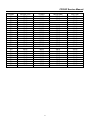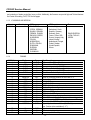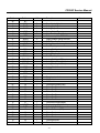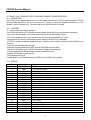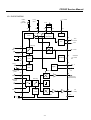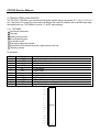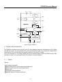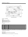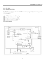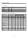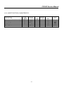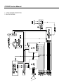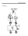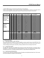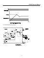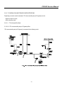
1
S/M No.TCP830FEF0
CHASSIS : CP-830F
MODEL : DTH-29U7
DTH-29U8
DTH-2881
DTH-28W8
DTH-28W9
OTC 2003
CP830F Service Manual
CONTENTS
DOCUMENT HISTORY
1 MAIN FEATURES
1.1 SPECIFICATIONS
1.1.1 GENERAL
1.1.2 EURO-SCART 1 (21 Pin)
1.1.3 EURO-SCART 2 (21 Pin)
1.2 CHANNEL/FREQUENCY TABLE
1.3 ATSS SORTING METHOD
1.3.1 GENERAL CASE
1.3.2 SPECIAL CASE
2 SAFETY INSTRUCTION
3 ALIGNMENT INSTRUCTIONS
3.1 MICROCONTROLLER CONFIGURATION : SERVICE MODE
3.2 SERVICE MODE NAVIGATION
3.3 MICROCONTROLLER CONFIGURATION : OPTION BITS
3.3.1 OPTION 1
3.3.2 OPTION 2
3.4 TV SET ALIGNMENT
3.4.1 LOCAL OSCILLATOR ALIGNMENT
3.4.2 G2 ALIGNMENT
3.4.3 WHITE BALANCE
3.4.4 FOCUS
3.4.5 VERTICAL GEOMETRY
3.4.6 HORIZONTAL PICTURE CENTRING
3.4.7 EAST / WEST CORRECTION
3.4.8 AGC
4 IC DESCRIPTION
4.1 TELETEXT DECODER WITH EMBEDDED 8-BIT CONTROLLER
4.1.1 BLOCK DIAGRAM OF THE SDA55XX
4.1.2 DESCRIPTION
4.1.3 IC MARKING AND VERSION
4.1.4 PINNING
4.2 VSP9412A - SCAN RATE CONVERTER INCLUDING MULTISTANDARD COLOUR
DECODER
4.2.1 BLOCK DIAGRAM OF THE VSP9412A
4.2.2 DESCRIPTION
4.2.3 PINNING
4.3 DDP 3315C - DISPLAY AND DEFLECTION PROCESSOR
4.3.1 BLOCK DIAGRAM OF THE DDP 3315C
4.3.2 DESCRIPTION
4.3.3 PINNING
4.4 MSP341X MULTISTANDARD SOUND PROCESSOR
4.4.1 BASIC FEATURES OF THE MSP 341X
4.4.1.1 Demodulator & NICAM Decoder Section
4.4.1.2 DSP-Section (Audio Baseband Processing)
-1-
5
5
5
5
5
6
7
10
10
10
12
13
13
13
13
14
14
14
14
14
15
15
15
15
15
16
17
17
17
17
18
18
19
20
20
22
23
24
24
26
28
28
28
29
CP830F Service Manual
4.4.1.3 Analogue Section
4.4.1.4 NICAM & FM/AM-Mono
4.4.1.5 German 2-Carrier System (DUAL FM System)
4.5 TDA4470 - MULTISTANDARD VIDEO-IF AND QUASI PARALLEL SOUND PROCESSOR
4.5.1 DESCRIPTION
4.5.2 FEATURES
4.5.3 PINNING
4.5.4 BLOCK DIAGRAM
4.6 TDA894XJ STEREO AUDIO AMPLIFIER
4.6.1 FEATURES
4.7 TDA835XJ VERTICAL AMPLIFIER
4.7.1 TDA8357J
4.7.2 TDA8358J
4.8 TDA6107Q
4.9 24C16 - 16 KB EEPROM
4.10 STR - F6654
4.10.1 GENERAL DESCRIPTION
4.10.2 FEATURES
4.10.3 BLOCK DIAGRAM
4.10.4 PIN DESCRIPTION
4.10.5 CONTROL PART - ELECTRICAL CHARACTERISTICS
4.10.6 MOSFET ELECTRICAL CHARACTERISTICS
5 CP830 CHASSIS DESCRIPTION
5.1 BLOCK DIAGRAM
5.2 IF SECTION
5.2.1 BLOCK DIAGRAM
5.2.2 VISION IF AMPLIFIER
5.2.3 TUNER-AND VIF-AGC
5.2.4 FPLL, VCO AND AFC
5.2.5 VIDEO DEMODULATION AND AMPLIFIER
5.2.6 SOUND IF AMPLIFIER AND SIF-AGC
5.2.7 QUASI-PARALLEL-SOUND (QPS) MIXER
5.2.8 STANDARD SWITCH
5.2.9 L SWITCH
5.2.10 INTERNAL VOLTAGE STABILISER
5.3 VIDEO / RGB 51
5.3.1 FRONT END
5.3.1.1 CVBS Front-End
5.3.1.2 Input Selector
5.3.1.3 Signal Levels And Gain Control
5.3.1.4 Synchronization
5.3.1.5 Chroma Decoder
5.3.1.6 Luminance Processing
5.3.1.7 RGB Front-End
5.3.1.8 Signal Processing
5.3.1.8.1 Horizontal Prescaler
5.3.1.8.2 Noise Reduction
5.3.1.8.3 Noise Measurement
5.3.1.8.4 Operation Modes
-2-
29
29
29
32
32
32
32
33
34
34
35
35
37
39
40
41
41
41
41
42
42
43
44
44
45
45
46
46
46
47
47
47
47
47
47
47
47
48
48
48
48
48
48
48
48
49
49
49
CP830F Service Manual
5.3.1.8.5 Digital 656 Output
5.3.2 BACK END
5.3.2.1 Digital Input Interface
5.3.2.2 Horizontal Scaler
5.3.2.3 Luma Contrast and Brightness
5.3.2.4 Black Level Expander/Compressor (BLEC)
5.3.2.5 Luma Sharpness Enhancer (LSE)
5.3.2.6 Dynamic Peaking
5.3.2.7 Luma Transient Improvement (LTI)
5.3.2.8 Mixing of Dynamic Peaking and LTI
5.3.2.9 Chroma Transient Improvement
5.3.2.10 Analog Back End
5.3.2.11 Analog RGB Insertion
5.3.2.12 CRT Measurement and Control
5.3.2.13 Synchronization and Deflection
5.3.2.14 EHT Compensation
5.4 MICROCONTROLLER
5.4.1 MICROCONTROLLER FEATURES
5.4.2 ACQUISITION FEATURES
5.4.3 PORTS
5.4.4 -CONTROLLER I/O PIN CONFIGURATION AND FUNCTION TABLE
5.4.5 TUNING
5.4.6 AUTOMATIC PICTURE FORMAT SWITCHING
5.4.6.1 WSS Data
5.4.6.2 SCART Pin 8 Data (Slow Switching)
5.4.6.3 Picture Format Description
5.4.6.3.1 16:9 CRT
5.4.6.3.2 4:3 CRT
5.4.7 EXTERNAL SOURCE CONTROL LOGIC
5.4.8 OVER CURRENT PROTECTION
5.5 TELETEXT DISPLAY
5.6 SOUND PROCESSING
5.6.1 ANALOGUE SOUND IF - INPUT SECTION
5.6.2 QUADRATURE MIXERS
5.6.3 PHASE AND AM DISCRIMINATION
5.6.4 NICAM DECODER
5.6.5 DSP SECTION
5.6.6 SOUND MODE SWITCHING
5.7 SOUND AMPLIFICATION
5.7.1 POWER AMPLIFIER
5.7.2 MODE SELECTION
5.8 VERTICAL DEFLECTION
5.8.1 FLYBACK VOLTAGE
5.8.2 PROTECTION
5.8.3 GUARD CIRCUIT
5.8.4 DAMPING RESISTOR
5.8.5 EAST-WEST AMPLIFIER (TDA8358J ONLY)
5.9 POWER SUPPLY (STR F6654)
5.9.1 STR-F6654 GENERAL DESCRIPTION
-3-
49
49
49
49
49
49
50
50
50
50
50
51
51
51
52
52
52
52
53
53
53
54
54
54
55
55
55
56
57
58
58
59
59
59
59
60
60
60
60
60
60
61
61
61
61
61
61
61
61
CP830F Service Manual
6
7
8
9
5.9.2 POWER SUPPLY PRIMARY PART OPERATIONS
5.9.2.1 Start -up Circuit: VIN
5.9.2.2 STR-F6654 Oscillating Operation
5.9.2.3 STR-F6654 Protection Circuits
5.10 TV START-UP, TV NORMAL RUN AND STAND BY MODE OPERATIONS
5.10.1 TV START-UP OPERATIONS
5.10.1.1 Schematic Diagram For Start-Up Operations
5.10.1.2 TV Start-Up And Microcontroller Initialisation
5.10.2 TV NORMAL RUN AND STAND-BY MODE OPERATIONS
5.10.2.1 TV On Normal Run Mode
5.10.2.2 TV Set On Stand-By Mode
SERVICE PARTS LIST
6.1 DTH-29U7ZL
6.2 DTG-2881ZL
EXPLODED VIEW
7.1 DTH-29U7
7.2 DTH-29U8
7.3 DTH-2881
7.4 DTH-28W8
7.5 DTG-28W9
PRINTED CIRCULT BOARD
8.1 MAIN PCB
8.2 CRT PCB
8.3 PFC PCB
SCHEMATIC DIAGRAM
-4-
61
62
63
64
65
65
65
65
67
67
70
72
72
80
88
88
89
90
91
92
93
93
94
95
96
CP830F Service Manual
DOCUMENT HISTORY
VERSION
V1.00
V1.01
DATE
18/11/02
22/11/02
COMMENTS
Creation of document (Author M Hearn) for project CP830 100Hz TV.
Reformatting of the document, plus insertion of Document History section
1 MAIN FEATURES
1.1 SPECIFICATIONS
1.1.1 GENERAL
TV standard
Colour system
Tuner
AV
Sound system
Power
consumption
Sound Output Power
Speaker
Teletext system
Aerial input
Channel coverage
Tuning system
Visual screen size
Channel indication
Program Selection
Aux. terminal
Remote Control
PAL - SECAM B/G D/K, PAL I/I, SECAM L/L
PAL, SECAM
PAL, SECAM, PAL 60, NTSC M, NTSC 4.43
NICAM B/G, I, D/K, L,
FM 2Carrier B/G, D/K
29"(4:3) Real Flat :84W approx.
28"(16:9) Real Flat : 84W approx.
7W x 2 (at 60% mod, 10%THD)
12W 8 ohm x2
9 pages memory FASTEXT (FLOF or TOP)
75 ohm unbalanced
Off-air channels, S-cable channels and hyperband
frequency synthesiser tuning system
28" : 66cm
29" : 68cm
On Screen Display
100 programmes
EURO-SCART 1 : Audio / Video In and Out, R/G/B
In, Slow and Fast switching.
EURO-SCART 2 : Audio / Video In and Out, SVHS In.
AV3 : Audio-Video Jack on front of cabinet.
Headphone jack (3.5 mm) on front of cabinet
SVHS3 (option) : Jack on front of cabinet ? sound
input common with AV3.
R-46G22
Unit
1.1.2 EURO-SCART 1 (21 Pin)
Pin
Signal Description
1
Audio Output Right
2
Audio Input Right
3
Audio Output Left
4
Audio Earth
5
Blue Earth
6
Audio Input Left
7
Blue Input
Matching value
0.5 Vrms, Impedance < 1 k , ( RF 54% Mod )
0.5 Vrms, Impedance > 10 k
0.5 Vrms, Impedance < 1 k , ( RF 54% Mod )
0.5 Vrms, Impedance > 10 k
0.7 Vpp 0.1V, Impedance 75
-5-
CP830F Service Manual
9
10
11
12
13
14
15
16
17
18
19
20
21
Green Earth
N.C.
Green Input
N.C.
Red Earth
Blanking Earth
Red Input
Fast Switching
Video Out Earth
Video In Earth
Video Output
Video Input
Common Earth
0.7 Vpp
0.1V, Impedance 75
0.7 Vpp 0.1V, Impedance 75
0 to 0.4V : Logic 0 , 1 to 3V : Logic 1 , Impedance 75
1 Vpp
1 Vpp
3dB, Impedance 75
3dB, Impedance 75
1.1.3 EURO-SCART 2 (21 Pin)
Pin
1
2
3
4
5
6
7
8
9
10
11
12
13
14
15
16
17
18
19
20
21
Signal Description
Audio Output Right
Audio Input Right
Audio Output Left
Audio Earth
Earth
Audio Input Left
N.C.
N.C.
N.C.
N.C.
N.C.
N.C.
Earth
Earth
Chroma Input
N.C.
Earth
Video In Earth
Video Output
Video Input, Y In.
Common Earth
Matching value
0.5 Vrms, Impedance < 1 k ( RF 54% Mod )
0.5 Vrms, Impedance > 10 k
0.5 Vrms, Impedance < 1 k , ( RF 54% Mod )
0.5 Vrms, Impedance > 10 k
3dB for a luminance signal of 1 Vpp
1 Vpp
1 Vpp
3dB, Impedance 75
3dB, Impedance 75
20 18 16 14 12 10 8
21 19 17 15 13 11 9
-6-
6
7
4
5
( Monitor output )
2
3
1
CP830F Service Manual
1.2 CHANNEL/FREQUENCY TABLE
CHANNEL
C01
C02
C03
C04
C05
C06
C07
C08
C09
C10
C11
C12
C13
C14
C15
C16
C17
C18
C19
C20
C21
C22
C23
C24
C25
C26
C27
C28
C29
C30
C31
C32
C33
C34
C35
C36
C37
C38
C39
C40
C41
C42
C43
C44
C45
EUROPE CCIR
46.25
48.25
55.25
62.25
175.25
182.25
189.25
196.25
203.25
210.25
217.25
224.25
53.75
82.25
183.75
192.25
201.25
471.25
479.25
487.25
495.25
503.25
511.25
519.25
527.25
535.25
543.25
551.25
559.25
567.25
575.25
583.25
591.25
599.25
607.25
615.25
623.25
631.25
639.25
647.25
655.25
663.25
FRANCE
55.75 (L )
60.5 (L )
63.75 (L )
176.00
184.00
192.00
200.00
208.00
216.00
189.25 (LUX)
69.25 (L )
76.25 (L )
83.25 (L )
90.25
97.25
471.25
479.25
487.25
495.25
503.25
511.25
519.25
527.25
535.25
543.25
551.25
559.25
567.25
575.25
583.25
591.25
599.25
607.25
615.25
623.25
631.25
639.25
647.25
655.25
663.25
-7-
GB(IRELAND)
45.75
53.75
61.75
175.25
183.25
191.25
199.25
207.25
215.25
223.25
231.25
239.25
247.25
49.75
57.75
65.75
77.75
85.75
471.25
479.25
487.25
495.25
503.25503.25
511.25
519.25
527.25
535.25
543.25
551.25
559.25
567.25
575.25
583.25
591.25
599.25
607.25
615.25
623.25
631.25
639.25
647.25
655.25
663.25
EAST OIRT
49.75
59.25
77.25
85.25
93.25
175.25
183.25
191.25
199.25
207.25
215.25
223.25
471.25
479.25
487.25
495.25
511.25
519.25
527.25
535.25
543.25
551.25
559.25
567.25
575.25
583.25
591.25
599.25
607.25
615.25
623.25
631.25
639.25
647.25
655.25
663.25
CP830F Service Manual
CHANNEL
C46
C47
C48
C49
C50
C51
C52
C53
C54
C55
C56
C57
C58
C59
C60
C61
C62
C63
C64
C65
C66
C67
C68
C69
C70
C71
C72
C73
C74
C75
C76
C77
S01
S02
S03
S04
S05
S06
S07
S08
S09
S10
S11
S12
S13
S14
S15
S16
EUROPE CCIR
671.25
679.25
687.25
695.25
703.25
711.25
719.25
727.25
735.25
743.25
751.25
759.25
767.25
775.25
783.25
791.25
799.25
807.25
815.25
823.25
831.25
839.25
847.25
855.25
863.25
69.25
76.25
83.25
90.25
97.25
59.25
93.25
105.25
112.25
119.25
126.25
133.25
140.25
147.25
154.25
161.25
168.25
231.25
238.25
245.25
252.25
259.25
266.25
FRANCE
671.25
679.25
687.25
695.25
703.25
711.25
719.25
727.25
735.25
743.25
751.25
759.25
767.25
775.25
783.25
791.25
799.25
807.25
815.25
823.25
831.25
839.25
847.25
855.25
863.25
104.75
116.75
128.75
140.75
152.75
164.75
176.75
188.75
200.75
212.75
224.75
236.75
248.75
260.75
272.75
284.75
-8-
GB(IRELAND)
671.25
679.25
687.25
695.25
703.25
711.25
719.25
727.25
735.25
743.25
751.25
759.25
767.25
775.25
783.25
791.25
799.25
807.25
815.25
823.25
831.25
839.25
847.25
855.25
863.25
103.25
111.25
119.25
127.25
135.25
143.25
151.25
159.25
167.25
255.25
263.25
271.25
279.25
EAST OIRT
671.25
679.25
687.25
695.25
703.25
711.25
719.25
727.25
735.25
743.25
751.25
759.25
767.25
775.25
783.25
791.25
799.25
807.25
815.25
823.25
831.25
839.25
847.25
855.25
863.25
105.25
112.25
119.25
126.25
133.25
140.25
147.25
154.25
161.25
168.25
231.25
238.25
245.25
252.25
259.25
266.25
CP830F Service Manual
CHANNEL
S17
S18
S19
S20
S21
S22
S23
S24
S25
S26
S27
S28
S29
S30
S31
S32
S33
S34
S35
S36
S37
S38
S39
S40
S41
EUROPE CCIR
273.25
280.25
287.25
294.25
303.25
311.25
319.25
327.25
335.25
343.25
351.25
359.25
367.25
375.25
383.25
391.25
399.25
407.25
415.25
423.25
431.25
439.25
447.25
455.25
463.25
FRANCE
296.75
136.00
160.00
303.25
311.25
319.25
327.25
335.25
343.25
351.25
359.25
367.25
375.25
383.25
391.25
399.25
407.25
415.25
423.25
431.25
439.25
447.25
455.25
463.25
-9-
GB(IRELAND)
287.25
295.25
303.25
311.25
319.25
327.25
335.25
343.25
351.25
359.25
367.25
375.25
383.25
391.25
399.25
407.25
415.25
423.25
431.25
439.25
447.25
455.25
463.25
EAST OIRT
273.25
280.25
287.25
294.25
303.25
311.25
319.25
327.25
335.25
343.25
351.25
359.25
367.25
375.25
383.25
391.25
399.25
407.25
415.25
423.25
431.25
439.25
447.25
455.25
463.25
CP830F Service Manual
1.3 ATSS SORTING METHOD
The TV set sweeps all the TV bands from beginning of VHF to end of UHF. The TV controlling software for each
program checks if a VPS CNI code is transmitted (this system exists for German, Swiss and Austrian transmissions).
If no VPS CNI code is found, then the system checks if a CNI code is transmitted as part of the teletext transmission
( Packet 8/30 format 1 and format 2). If such a code ( VPS or teletext ) is found and if this code is in the ATSS list, the
program is automatically named.
If the transmission does not have VPS CNI, and no teletext service is available, then there is no possibility of the
program being automatically named.
The programs found are then sorted in 4 groups :
Group I : It contains all the programs from the selected country and named by the TV controlling software. Within this
group the sorting order is fixed by the ATSS list.
Group II : It contains all the programs with a strong signal strength which are not listed in group I.
Group III : It contains all the programs with a weak signal strength which are not listed in group I.
Group IV : If two or more programs with the same code are found, only the strongest ( or if they have the same level
the one with the lowest frequency) is listed in group I, II or III. The others are listed in group IV.
1.3.1 GENERAL CASE
Program
number
1
2
...
n
n+1
...
m
m+1
...
p
p+1
...
q
q+1
...
99
0
1.3.2 SPECIAL CASE
Group
Program
number
1
...
m
m+1
...
p
p+1
...
q
q+1
...
99
0
Skip
Group I
Group II
Group III
Group IV
Group
Group II
Group III
Group IV
not used
Special case : Country selection = Others
not used
-10-
Skip
CP830F Service Manual
Note : If two programs with the same name but a different code are found these two programs
are listed in group I, II or III .
The sorting order within group II, III, and IV is based on the channel frequency. The program
with the lowest frequency is allocated the first rank in its group, and so forth until the last
program of the group which has the highest frequency.
Special case : France
If France is selected, the TV controlling software first sweeps all TV bands with France system
selected ( positive video modulation) and then a second time with Europe system selected (
negative video modulation).
Special case : Switzerland
If Switzerland is selected the TV controlling software first sweeps all TV bands with Europe
system selected (negative video modulation) and then a second time with France system
selected ( positive video modulation).
Special case : GB
Note for satellite receiver users : Before starting ATSS turn on your satellite receiver and tune to
SKY NEWS .
If GB is selected the TV controlling software seeks for programs only in UHF ( C21 to C70 ).
The
sorting order is :
1 - BBC1
2 - BBC2
3 - ITV
4 - CH4
5 - CH5
6 ? NEWS (Sky News)
If two or more identical programs ( same name but different code e.g. BBC1 and BBC1
Scotland ) are found the following programs in the list will be shifted up. (1 - BBC1, 2 - BBC1, 3
BBC2, 4 - ITV, 5 - CH4, 6 - CH5, 7 - NEWS, ..)
If one of the programs above is not found, the associated program number remains empty (
freq.=467.25 MHz - Skip selected - no name ? system = GB).
example A : 1 - BBC1, 2 - BBC2, 3 - ITV, 4 - -----, 5 - CH5, 6 - NEWS, ...
example B ( if 2 BBC1 found ) : 1 - BBC1, 2 - BBC1, 3 - BBC2, 4 - ITV, 5 - -----, 6 - CH5, 7 NEWS, ...
-11-
CP830F Service Manual
2 SAFETY INSTRUCTION
WARNING: Only competent service personnel may carry out work involving the testing or repair
of this equipment.
X-RAY RADIATION PRECAUTION
1. Excessive high voltage can produce potentially hazardous X-RAY RADIATION. To avoid
such hazards, the high voltage must not exceed the specified limit. The nominal value of the
high
voltage of this receiver is 25-26 KV (20 -21 ) or 26 KV (25 - 28 ) at max beam current. The
high
voltage must not, under any circumstances, exceed 27.5 KV (20 ), 29KV (21 ), 29.5 KV (25 )
or
30 KV (28 ). Each time a receiver requires servicing, the high voltage should be checked. It is
important to use an accurate and reliable high voltage meter.
2. The only source of X-RAY Radiation in this TV receiver is the picture tube. For continued
X-RAY RADIATION protection, the replacement tube must be exactly the same type tube as
specified in the parts list.
SAFETY PRECAUTION
Potentials of high voltage are present when this receiver is operating. Operation of the receiver
outside the cabinet or with the back board removed involves a shock hazard from the receiver.
Servicing should not be attempted by anyone who is not thoroughly familiar with the
precautions
necessary when working on high voltage equipment.
Discharge the high potential of the picture tube before handling the tube. The picture tube is
highly evacuated and if broken, glass fragments will be violently expelled.
If any Fuse in this TV receiver is blown, replace it with the FUSE specified in the Replacement
Parts List.
When replacing a high wattage resistor (metal oxide film resistor) in the circuit board, keep the
resistor 10 mm away from circuit board.
Keep wires away from high voltage or high temperature components.
This receiver must operate under AC 230 volts, 5O Hz. NEVER connect to a DC supply or any
other voltage or frequency.
PRODUCT SAFETY NOTICE
Many electrical and mechanical parts in this equipment have special safety-related
characteristics. These characteristics are often passed unnoticed by a visual inspection and the
X-RAY RADIATION protection afforded by them cannot necessarily be obtained by using
replacement components rated for higher voltage, wattage, etc. Replacement parts which have
these special safety characteristics are identified in this manual and its supplements, electrical
components having such features are identified by designated symbol on the parts list. Before
replacing any of these components, read the parts list in this manual carefully. The use of
substitutes replacement parts which do not have the same safety characteristics as specified in
the parts list may create X-RAY Radiation.
-12-
CP830F Service Manual
3 ALIGNMENT INSTRUCTIONS
3.1MICROCONTROLLER CONFIGURATION : SERVICE MODE
To switch the TV set into service mode please see instruction below.
1 - Select PR. number 91
2 - Adjust sharpness to minimum and exit all menus.
3 - Within 2 seconds press the key sequence : RED - GREEN - menu
The software version is displayed beside the word Service, e.g. SERVICE V1.00 .
To exit SERVICE menu press menu key or Std By key.
3.2SERVICE MODE NAVIGATION
Pr Up/Down remote keys : cycle through the service items available.
Vol -/+ remote keys
: Dec./Increment the values within range - Cycle trough option bits.
OK key
: Toggle bits in option byte
Order
1
2
3
4
5
6
7
8
9
10
11
12
13
14
15
16
17
18
19
20
21
Item
HOR CEN
RED GAIN
GRN GAIN
BLUE GAIN
RED BIAS
GRN BIAS
AGC LEVEL
G2 - SCREEN
AFT
OPTION1
OPTION2
PARABOLA
HOR WIDTH
CORNER T
CORNER B
HOR. PARAL
V. LINEAR
EW TRAPEZ
S CORRECT
VERT CENT
VERT SIZE
Default setting
3.3 MICROCONTROLLER CONFIGURATION : OPTION BITS
There are two option bytes available (16 bits in all). These option bits are available from Service
mode. First find the OPTION1 or OPTION2 control, and then use the Volume PLUS/MINUS
buttons on the remote control keypad to locate the bits, and OK key to toggle them. The table
below shows the two option bytes available;
-13-
CP830F Service Manual
3.3.1 OPTION 1
1
0
B7
TOP
text
OFF
TOP
text ON
B6
FASTEXT
(FLOF)
OFF
FASTEXT
(FLOF)
ON
B5
TUBE
4:3
TUBE
16:9
B4
Headphone
Volume/Balance
control OFF
Headphone
Volume/Balance
control ON
B3
Dolby
Virtual
OFF
Dolby
Virtual
ON
B2
SVHS
3
disable
SVHS
3
enable
B1
B0
Tuner options
00 = Philips
01 = not used
10 = ALPS
11 = PARTSNIC
(DW)
3.3.2 OPTION 2
B7
B6
B5
B4
B3
B2
B1 B0
1 Fixed to ‘0’ JVC remote control AVL control OFF PICTURE TILT ON Program list enabled See table below.
0
Daewoo Remote control AVL control ON PICTURE TILT OFF Program list disabled
Beam Current
Tube
(mA)
B2
B1
B0
Nominal
Max
0.95
1.10
0
0
0
1.00
1.15
0
0
1
1.05
1.20
0
1
0
1.10
1.25
0
1
1
1.20
1.35
1
0
0
1.25
1.40
1
0
1
1.30
1.45
1
1
0
1.35
1.50
1
1
1
4/3 - Super Flat, 16/9 – Super Flat
4/3 - Real Flat, 16/9 – Real Flat
All values modified are immediately memorised in eeprom.
3.4 TV SET ALIGNMENT
3.4.1 LOCAL OSCILLATOR ALIGNMENT
Tune a colour bar pattern. The frequency of the signal carrier must be accurate ( Max +/- 10KHz deviation from the
nominal channel frequency).
Find AFT item in service mode.
Adjust the coil L150 to bring the cursor to central position : 32.
3.4.2 G2 ALIGNMENT
- Tune a colour bar pattern.
- Find the G2 - SCREEN item in service mode.
- Adjust screen volume ( on FBT ) to bring the cursor to central position : 32.
-14-
CP830F Service Manual
3.4.3 WHITE BALANCE
- Select a dark picture and adjust RED BIAS and GRN BIAS to the desired colour temperature.
- Select a bright picture and adjust RED, GRN and BLUE GAIN to the desired colour temperature.
3.4.4 FOCUS
Adjust the Focus volume ( on FBT ) to have the best resolution on screen.
3.4.5 VERTICAL GEOMETRY
Adjust V. LINEAR (linearity), S CORRECT (S. Correction), VERT SIZE (Vertical amplitude), VERT CENT (vertical
centring) to compensate for vertical distortion.
3.4.6 HORIZONTAL PICTURE CENTRING
Adjust HOR CEN (Horizontal centre) to have the picture in the centre of the screen.
3.4.7 EAST / WEST CORRECTION
Adjust the PARABOLA, HOR WIDTH, CORNER, HOR PARAL, EW TRAPEZ, to compensate for
geometrical distortion.
HOR PARAL
HOR WIDTH
adjust for 93% overscan.
-15-
CP830F Service Manual
PARABOLA
CORNER B & CORNER T
EW TRAPEZ
3.4.8 AGC
- Make sure option bits are correct for the tuner fitted on the chassis (See above how to change option bits).
- Adjust the antenna signal level at 64 dB V± 2
- Tune a colour bar pattern.
- Find the AGC item in service mode.
- Press the key OK on the remote keypad and wait until AGC level stabilise to the optimum value.
- Alternatively, use Vol Up/Dwn keys to adjust manually to the desired Tuner Take Over Point (TOP).
-16-
CP830F Service Manual
4 IC DESCRIPTION
4.1 TELETEXT DECODER WITH EMBEDDED 8-BIT CONTROLLER
TVText Pro is a 8-bit controller based on a enhanced 8051 core with embedded teletext, On screen Display and TV
controller functions.
4.1.1 BLOCK DIAGRAM OF THE SDA55XX
4.1.2 DESCRIPTION
The SDA 55xx is a single chip teletext decoder for decoding World System Teletext data as well as Video
Programming System (VPS), Program Delivery Control (PDC), and Wide Screen Signalling (WSS) data used for PAL
plus transmissions (line 23).
The device provides an integrated general-purpose, fully 8051-compatible Microcontroller with television specific
hardware features. The microcontroller has been enhanced to provide powerful features such as memory banking,
data pointers and additional interrupts etc.
The on-chip display unit for displaying Level 1.5 teletext data is also used for customer defined on-screen displays.
Internal XRAM consists of 16 Kbytes. Device has an internal ROM of 128 Kbytes.
The SDA 55xx supports a wide range of standards including PAL, NTSC and contains a digital slicer for VPS, WSS,
PDC, TTX and Closed Caption, an accelerating acquisition hardware module, a display generator for Level 1.5 TTX
data and powerful On screen Display capabilities based on parallel attributes, and Pixel oriented characters (DRCS).
The 8-bit Microcontroller runs at 360 ns. cycle time (min.). Controller with dedicated hardware does most of the
internal TTX acquisition processing, transfers data to/from external memory interface and receives/transmits data via I
2 C-firmware user-interface. The slicer combined with dedicated hardware stores TTX data in a VBI buffer of 1
Kilobyte. The Microcontroller firmware performs all the acquisition tasks (hamming-and parity-checks, page search
-17-
CP830F Service Manual
and evaluation of header control bits) once per field. Additionally, the firmware can provide high-end Teletext-features
like Packet-26-handling, FLOF, TOP and list-pages.
4.1.3 IC MARKING AND VERSION
Chassis
CP830
4.1.4
IC marking
OSD languages
BULGARIAN,
CZECH, GERMAN,
DANISH, SPANISH,
FRENCH, FINNISH,
ENGLISH, GREEK,
HUNGARIAN,
ITALIAN,
NORWEGIAN,
DUTCH, POLISH,
ROMANIAN,
RUSSIAN,
SWEDISH,
SLOVAKIAN.
ATSS countries
Austria, Belgium,
Switzerland, Czech
Republic, Germany,
Denmark, Spain,
France, Finland, GB,
Greece, Hungary, Italy,
Ireland, Norway,
Netherlands, Portugal,
Poland, Sweden,
Slovak Republic,
Others
Text
PAN-EUROPEAN
LATIN, CYRILLIC,
GREEK.
PINNING
PSDIP 52-pin
1
2
3
4
5
6
7
8
9
10
11
12
13
14
15
16
17
18
19
20
21
Pin Name
SCL
SDA
S/SW2
S/SW2
S/SW1
S/SW1
n.c.
Reset Out
VDD2.5
VSS
VDD3.3
CVBS
VDDA2.5
VSSA
AFT
AGC
KEY
OCP
HS
VS
MODESW
Type
IN/OUT
IN/OUT
IN
IN
IN
IN
22
23
24
L/L
IR
INT
OUT
IN
IN
OUT
IN
IN
IN
IN
IN
IN
IN
IN
IN
IN
IN
IN
OUT
Short Description
Software driven I2C bus Clock line
Software driven I2C bus Data line
Slow switching control for SCART 2.
(See Microcontroller I/O pin configuration)
Slow switching control for SCART 1.
(See Microcontroller I/O pin configuration)
Driven by controlling software to reset video IC s.
Supply voltage 2.5V
Ground (0V)
Input/Output 3.3V
CVBS input for the acquisition circuit
Supply voltage for analog components
Ground for analog components
ADC input, AFT input
ADC input, for AGC alignment only
ADC input, local key sensing
Switch Off the set when the voltage goes below a trigger level
Horizontal sync for OSD/Txt synchronisation
Vertical sync for OSD/Txt synchronisation
High : Negative video modulation (B, G, D, K,I)
Low : Positive video modulation (L / L )
High : L , Low : L
Remote control signal input
Interrupt input from audio processor
-18-
CP830F Service Manual
PSDIP 52-pin
25
26
27
28
29
30
31
32
33
34
35
36
37
38
39
40
41
42
43
44
45
46
47
48
49
50
51
52
Pin Name
n.c.
n.c.
n.c.
n.c.
VSS
VDD3.3
n.c.
n.c.
RESET
XTAL2
XTAL1
VSSA
VDDA2.5
R OUT
G OUT
B OUT
BK OUT
VDD2.5
VSS
VDD3.3
n.c.
n.c.
n.c.
AGC
n.c.
n.c.
LED
POWER
Type
Short Description
IN
IN
Ground (0V)
Input/Output 3.3V
IN
OUT
IN
IN
IN
OUT
OUT
OUT
OUT
IN
IN
IN
A low level on this pin resets the device.
Output of the inverting oscillator amplifier
Input of the inverting oscillator amplifier
Ground for analog components
Supply voltage for analog components
Red output
Green output
Blue output
Blanking
Supply voltage 2.5V
Ground (0V)
Input / Output 3.3V
OUT
Tuner TOP adjustment
OUT
OUT
High : Green LED, Low : Red LED
High : SMPS ON, Low : SMPS in stand by
4.2 VSP9412A - SCAN RATE CONVERTER INCLUDING MULTISTANDARD COLOUR DECODER
The VSP 94x2A comprises all main functions of a digital featurebox in one monolithic IC.
The device comprises a digital multistandard color decoder, a RGB interface with fast-blank capability (SCART), digital
ITU656 input, scaling units including panorama, embedded DRAM for upconversion, picture improvements, temporal
noise reduction as well as A/D and D/A converter.
-19-
CP830F Service Manual
4.2.1 BLOCK DIAGRAM OF THE VSP9412A
Data
Acquisition
7
CVBS
(Y/C)
Input
Processing
Noise
Reduction
3
CVBS
(OUT)
2
G/Y
B/Cb
2
FBL
2
Mem. Controller
Field Memory
Source Select
A/D Conversion
Color Decoder
Frontend Sync
Soft Mix
2
R/Cr
Memory
Display
Processing
Hor. Scaling
Panorama
Peaking, CTI
Output
Processing
HOUT
VOUT
CLK27
Display Sync
4:2:2 Format
Y
Cr
Cb
D/A conversion
Oversampling
(9402/9432)
8
ITU 656
Clock
Generation
CLK 656
B
Digital Output
(9412/9442)
I2
C
SCL
Digital 656
CLK 656
SDA
20.25 MHz
cybs3
cybs4
cybs5
cybs6
Soruce
Select
(1)
gin1
rin2
gin2
bin2
fbt2
xout xin
Y
U,V
CVBS Frontend
Clock generation
(9/10/11)
Soruce
Select
ADCG
(13)
(16)
ADCB
(14)
Channel
mix
(31)
Soft-mix
(30)
Y
U,V
RBB Frontend
Sample tate
Converter
(33/34)
Noise
measurerrent
(32)
ADCF
(15)
memory
controller
(39)
Noise
reduction
(35/36/37/38)
PC
interface
(56)
test-controller,
memory hist
tclk
vout
hout
tms
adntd
scl
line locked or
free-running
sda
4.2.2 DESCRIPTION
Integrated Video Matrix switch
- Up to seven CVBS inputs, up to two Y/C inputs,
- Up to three CVBS outputs (even when Y/C input)
- 9 bit amplitude resolution for CVBS, Y/C A/D converter
- AGC (Automatic Gain Control)
-20-
Y DAC (52)
ayout
U DAC (53)
auout
V DAC (54)
avout
Peaking/DCTI/delzly
Panorama Scaler
(42/43/44/57)
CLKF20
656hinf 656vln
clkf20
clkout
eDRAM
ITO656
Decoder
(41)
CLKF2PAD
Output
Sync
Controller
(40)
PRIMUS
VSP94x2A
CLKB36
656clk
656io0
656io1
656io2
656io3
656io4
656io5
656io6
656io7
Output
Data
Controller
(55)
free-running
clocks
Iine-locked
clocks
(4/4/6/7/8)
ADCR
(12)
min1
fbt1
ADC1
(2)
ADC2
(2)
cybs7
bin1
h50 v50 v
data
cybs2
reset
buffer
cybs1
cybso3
data
cybso2
buffer
cybso1
(45/46/49/50)
8
ITU656 Encoder
(51)
CP830F Service Manual
Multi-standard colour decoder
- PAL/NTSC/SECAM including all substandards
- Automatic recognition of chroma standard
- Only one crystal necessary for all standards
RGB-FBL or YUV-H-V input
- 8 bit amplitude resolution for RGB or YUV
- 8 bit amplitude resolution for FBL or H
ITU656 support
- ITU656 output
- DS656 output (double-scan 656like output)
Noise reduction
- Motion adaptive temporal noise reduction
- Field-based temporal noise reduction for luminance and chrominance
- Different motion detectors for luminance and chrominance or identical
- Flexible programming of the temporal noise reduction parameters
- Automatic measurement of the noise level
Horizontal scaling of the 1fH signal
- Split-screen possible with additional PiP or Text processor
Flexible digital horizontal scaling of the 2fH signal (Not used in this chassis)
- Scaling factors: 3, ... [2 pixel resolution], ..., 0.75 including 16:9 compatibility
- 5 zone panorama generator
Embedded memory
- On-chip memory controller
- Embedded DRAM core for field memory
- SRAM for PAL/SECAM delay line
Data format 4:2:2
Flexible clock and synchronisation concept
- Horizontal line-locked or free-running mode
- Vertical locked or free-running mode
Scan-rate-conversion
- Simple interlaced modes (100/120 Hz): AABB, AAAA, BBBB (9402A/9412A only)
Flexible output sync controller
- Flexible positioning of the output signal
- Flexible programming of the output sync raster
- Blank signal generation
Signal manipulations
- Still field
- Insertion of coloured background
- Windowing
- Vertical chrominance shift for improved VCR picture quality
Sharpness improvement (not used in this chassis)
- Digital color transition improvement (DCTI)
- Peaking (luminance)
1920 active pixel/per line in default configuration
I2C-bus control (400 kHz)
- selectable I C address
1.8V 5% and 3.3V 5% supply voltages
P-MQFP-80 package
-21-
CP830F Service Manual
4.2.3 PINNING
Pin
52
53
54
55
56
57
58
63
62
61
70
69
23
17
3
2
1
80
79
78
77
76
75
39
40
41
37
46
47
48
38
14
6
13
7
19
24
27
59
60
50
51
64
65
44
Name
cvbs1
cvbs2
cvbs3
cvbs4
cvbs5
cvbs6
cvbs7
Cvbso1
Cvbso2
Cvbso3
Xin
Xout
Vout
Hout
i656i7
i656i6
i656i5
i656i4
i656i3
i656i2
i656i1
i656i0
i656iclk
Rin1
Gin1
Bin1
Fbl1
Rin2
Gin2
Bin2
Fbl2
V
Sda
Scl
Tms
Adr/tdi
Reset
Clkout
Vdd33c
Vss33c
Vddac1
Vssac1
Vddac2
Vssac2
Vdd33rgb
I/O
I
I
I
I
I
I
I
O
O
O
I
O
O
O
I
I
I
I
I
I
I
I
I
I
I
I
I
I
I
I
I
I
I/O
I
I
I
I
O
S
S
S
S
S
S
S
Description
CVBS input
CVBS input
CVBS input
CVBS input or Y1
CVBS input or C1
CVBS input or Y2
CVBS input or C2
CVBS output 1
CVBS output 2
CVBS output 3
Crystal connection 1
Crystal connection 2
Vertical output
Horizontal output
656 input (MSB)
656 input
656 input
656 input
656 input
656 input
656 input
656 input (LSB)
656 input clock
R in 1
G in 1
B in 1
Fast Blank input 1
R in 2
G in 2
B in 2
Fast Blank input 2
Vertical pulse for RGB input
I2C ?Bus data
I2C ?Bus clock
Test mode select
I2C Address / test data in
Reset input
Output clock
Supply voltage CVBS
Supply voltage CVBS
Supply voltage CVBS1
Supply voltage CVBS1
Supply voltage CVBS2
Supply voltage CVBS2
Supply voltage RGB
-22-
Remarks
Reset when low
27MHz
3.3V
0V
1.8V
0V
1.8V
0V
3.3V
CP830F Service Manual
Pin
45
42
43
35
36
68
66
67
5
4
28
29
34
33
72
73
12
11
25
26
71
18
20
32
31
30
22
21
16
15
10
9
74
Name
Vss33rgb
Vddargb
Vssargb
Vddafbl
Vssafbl
Vddapll
Vddd1
Vssdl
Vddd2
Vssd2
Vddd3
Vssd3
Vddd4
Vssd4
Vddp1
Vssp1
Vddp2
Vssp2
Vddp3
Vssp3
Tclk
H50
V50
656io0
656io1
656io2
656io3
656io4
656io5
656io6
656io7
656clk
656hin/clkf20
I/O
S
S
S
S
S
S
S
S
S
S
S
S
S
S
S
S
S
S
S
S
I
O
O
I/O
I/O
I/O
I/O
I/O
I/O
I/O
I/O
I/O
I/O
8
656vin/blank
I/O
49
Vssd5
S
Description
Supply voltage RGB
Supply voltage for RGB
Supply voltage for RGB
Supply voltage for FBL
Supply voltage for FBL
Supply voltage for PLL
Supply voltage for digital
Supply voltage for digital
Supply voltage for digital
Supply voltage for digital
Supply voltage for DRAM
Supply voltage for digital
Supply voltage for digital
Supply voltage for digital
Supply voltage for digital
Supply voltage for digital
Supply voltage for digital
Supply voltage for digital
Supply voltage for digital
Supply voltage for digital
Testclock
Hout 50 Hz
Vout 50 Hz
Digital input / output
Digital input / output
Digital input / output
Digital input / output
Digital input / output
Digital input / output
Digital input / output
Digital input / output
Digital input / output clock
Separate H input for 20.25 clock
output
Separate V input for 656 / BLANK
output
Supply voltage for digital
4.3 DDP 3315C - DISPLAY AND DEFLECTION PROCESSOR
The DDP 3315C is a mixed-signal single-chip digital display and deflection processor, designed
for high-quality backend applications in double scan and HDTV TV sets with 4:3 or 16:9 picture
tubes. The interfaces qualify the IC to be combined with state of the art digital scan rate
converters, as well as analog HDTV sources. The DDP 3315C contains the entire digital video
component, deflection processing, and all analog interfaces to display the picture on a CRT.
-23-
Remarks
0V
1.8V
0V
1.8V
0V
1.8V
1.8V digital
0V digital
1.8V digital
0V digital
1.8V digital
0V digital
1.8V digital
0V digital
3.3V pad
0V digital
3.3V pad
0V pad
3.3V pad
0V pad
Connect to vss
LSB
0V
CP830F Service Manual
R
G
B
FBL
4.3.1 BLOCK DIAGRAM OF THE DDP 3315C
SVM
Clock
Generator
Y/
656 YCrCb
CrCb
4:2:2 /
4:1:1
SDA
SCL
Input
Interface
UpconVersion/
Scaling
Y
Cb
Cr
Y
Picture
Cb
ImproveCr
ment
Matrix /
PFG /
NCE
R
G
B
SVM
Y
Cb
Cr
Pr
Y Input
Pb
FBL
analog
RGBMatrix
R
G
B
LLC
27/32/
54 MHz
R
G
B
Video
DAC
R
G
B
Analog
RGB
Switch
R
G
B
Tube
Control
R
G
B
Output
Sense
Input
I2C
Interface
Sawtooth /
Parabola
Generation
V
EHT
V
V
H&V
EW
H/V
EW
VERT+
VERT
E/W
General
purpose
PWM
Sync
Processing
PWM 1/2
2H / 2V
(1H / 1V)
V
H
DisplayFreq.
Doubling
H
FIFO
Controlling
H-Drive
Generation
HFLB
H
dynamic
focus
H
Security
Unit
HOUT
DFVBL
PWMV
VPROT
HSAFETY
4.3.2 DESCRIPTION
Video Processing
- linear horizontal scaling (0.25 ... 4), as well as nonlinear horizontal scaling panorama vision
- dynamic black level expander
- luma sharpness enhancement by dynamic peaking and luma transient improvement (LTI)
- color transient improvement (CTI)
- programmable RGB matrix
- black stretch, blue stretch, gamma correction via programmable Non-linear Colorspace Enhancer (NCE) on RGB
- two analog double scan inputs with fast blank (one RGB and one RGB/YC r C b /YP r P b selectable)
- average and peak beam current limiter
- automatic picture tube adjustment (cutoff, drive)
- histogram calculation
Deflection Processing
- scan velocity modulation output
- digital EHT compensation for vertical / east-west
- soft start/stop of horizontal-drive
- vertical angle and bow correction
- differential vertical outputs
- vertical zoom via deflection adjustment
- horizontal and vertical protection circuit
-24-
CP830F Service Manual
- horizontal frequency for VGA/SVGA/1080I
- black switch off procedure
- supports horizontal and vertical dynamic focus
Miscellaneous
- selectable ITU-R 601 4:1:1 / 4:2:2 YC r C b input at 27/32 MHz or double scan ITU-R 656 input at 54 MHz line-locked
clock
- crystal oscillator for horizontal safety
- picture frame generator
- hardware for simple 50/60 Hz to 100/120 Hz conversion (display frequency doubling)
- PQFP80 package, 5 V analog and 3.3 V digital supply
IC architecture
A clock generator converts different external line locked clock rates to a common internal sample rate of ~40 MHz, in
order to provide a higher horizontal resolution. The input interface accepts ITU-R 601 at 27 or 32 MHz and ITU-R 656
with encoded or external sync at 54 MHz. The horizontal scaler is used for the scan rate conversion and for the
nonlinear aspect ratio conversion as well.
For the picture improvement, luma and chroma are processed separately. The luminance contrast ratio can be
extended with a dynamic black level expander. In addition the frequency characteristic is improved by a transient
improvement (LTI) and an adaptive dynamic peaking circuit. The peaking adapts to small AC amplitudes of high
frequency parts, while large AC amplitudes are processed by the LTI. The chroma signal is enhanced with a transient
improvement (CTI) with proper limitation to avoid wrong colours. The full programmable RGB matrix covers control of
colour saturation and temperature. A digital white drive control is used to adjust the white balance and for the beam
current limitation to prevent the CRT from over-load. A non-linear colorspace enhancer (NCE) for RGB gives full
flexibility for any amplitude characteristic. High speed10-bit D/A converters are used to convert digital RGB to analog
signals. Separate 9-bit D/A converters control brightness and cutoff. For picture tubes equipped with an appropriate
yoke a scan velocity modulation (SVM) signal is calculated using a differentiated luminance signal.Two analog sources
can be inserted in the main RGB, controlled by separate fastblank (FBL) signals. Contrast and brightness are adjusted
separately from main RGB. One input is dedicated to RGB for on screen display (OSD). The second input is
processed with an analog RGB matrix to insert YCbCr/YpbPr or RGB with control of colour saturation and
programmable half contrast. The bandwidth of ~30MHz guarantees pixel based graphics to be displayed with full
accuracy. All previously mentioned features are implemented in dedicated hardware. An integrated processor controls
the horizontal and vertical deflection, tube measurement loops and beam current limitation. It is also used to calculate
an amplitude histogram of the displayed image.
The horizontal deflection is synchronized with two numeric phase-locked loops (PLL) to the incoming sync. One PLL
generates the horizontal timing signals, e.g. blanking and key-clamping. The second PLL adjusts the phase of the
horizontal drive pulse with a subpixel accuracy less than 1 ns.
Vertical deflection and east/west correction waveforms are calculated as 6th order polynomials. This allows adjustment
of an east/west parabola with trapezoidal, pincushion and an upper/lower corner correction (even for real flat CRT s),
as well as a vertical sawtooth with linearity and S-correction. Scaling both waveforms, and limiting to fix amplitudes,
performs a vertical zoom or compression of the displayed image. A field and line frequent control loop compensates
picture content depending EHT distortions.
-25-
CP830F Service Manual
4.3.3 PINNING
Pin No.
1
2
3
4
5
6
7
8
9
10
11
12
13
14
15
16
17
18
19
20
21
22
23
24
25
Pin Name
Y6
Y7
656EN
LLC2
HS
VS
FREQSEL
CM1
CM0
VS2
XTAL2
XTAL1
NC
GNDP
VSUPP
FIFORRD
FIFORD
FIFOWR
FIFORWR
PWM1
PWM2
PWMV
HOUT
VSTBY
DFVBL
I/O
I
I
I
I
I
I
I
I
I
I
O
I
Description
Picture bus Luma
Picture bus Luma (MSB)
Enable 656 input mode
System clock input
Horizontal Sync Input
Vertical Sync Input
Selection of H-Drive Frequency Range
Clock select 1
Clock select 0
Additionnal VSYNC input
Analog Crystal Output
Analog Crystal Input
S
S
O
O
O
O
O
O
O
O
S
O
26
27
28
29
30
31
32
33
34
35
36
37
38
39
HSYNC
VSYNC
NC
ASG1
HFBL
SAFETY
VPROT
RSW2
RSW1
SENSE
GNDM
VERT+
VERTEW
O
O
Ground, Output Pin Driver
Supply voltage, Output Pin Driver
FIFO Read Counter Reset
FIFO Read Enable
FIFO Write Enable
FIFO Write Counter Reset
I2C controlled DAC
I2C controlled DAC / Tilt output
I2C controlled DAC
Horizontal drive output
Standby supply voltage, Hout generation
Dynamic focus blanking / horizontal DAF
pulse
Horizontal sync output
Vertical sync output
S
I
I
I
O
I/O
I
S
O
O
O
Analog Shield Ground
Horizontal flyback input
Safety input
Vertical protection input
Range Switch2, measurement ADC
Range Switch1, measurement ADC
Sense ADC input
Ground, MADC input
Differential Vertical Sawtooth Output
Differential Vertical Sawtooth Output
East / West Correction Output
-26-
Remarks
CP830F Service Manual
Pin No.
40
41
42
43
44
45
46
47
48
49
50
51
52
53
54
55
56
57
58
59
60
61
62
63
64
65
66
67
68
69
70
71
72
73
74
75
76
77
78
79
80
Pin Name
NC
SVM
ROUT
GOUT
BUT
GNDO
XREF
VSUPO
VRD/BCS
AGND
FBLIN1
RIN1
GIN1
BIN1
FBLIN2
RIN2 / PR
GIN2 / Y
BIN2/ PB
ASG2
HCS
NC
TEST
RESQ
SCL
SDA
C0
C1
C2
C3
C4
C5
C6
C7
VSUPD
GNDD
Y0
Y1
Y2
Y3
Y4
Y5
I/O
Description
O
O
O
O
S
I
S
I
S
I
I
I
I
I
I
I
I
S
I
Scan Velocity Modulator
Analog Output Red
Analog Output Green
Analog Output Blue
Ground, analog Back End
Reference Input for RGB DAC s
Supply voltage, Analog Back End
DAC Reference, Beam current safety
Analog Ground for Analog Matrix
Fast Blank1input
Analog Red1input
Analog Green1 input
Analog Blue1input
Fast Blank2 input
Analog Red2 input / PR Input
Analog Green2 input / Y Input
Analog Blue2 input / PB Input
Analog Shield Ground
Half Contrast
I
I
I/O
I/O
I
I
I
I
I
I
I
I
S
S
I
I
I
I
I
I
Reset Input, active low
I2C Bus clock
I2C Bus data
Picture Bus Chroma (LSB)
Picture Bus Chroma
Picture Bus Chroma
Picture Bus Chroma
Picture Bus Chroma
Picture Bus Chroma
Picture Bus Chroma
Picture Bus Chroma (MSB)
Supply voltage, Digital Circuitry
Ground, Digital Circuitry
Picture Bus Luma (LSB)
Picture Bus Luma
Picture Bus Luma
Picture Bus Luma
Picture Bus Luma
Picture Bus Luma
-27-
Remarks
CP830F Service Manual
4.4 MSP341X MULTISTANDARD SOUND PROCESSOR
The MSP 341x is designed as a single-chip Multistandard Sound Processor for applications in analogue and digital TV
sets, video recorders, and PC cards.
The MSP3411 has all functions of MSP3410 with the addition of a virtual surround sound features.
Surround sound can be reproduced to a certain extent with two loudspeakers. The MSP3411 includes virtualizer
algorithm 3D Panorama which has been approved by the Dolby laboratories for compliance with the Virtual Dolby
Surround technology. In addition, the MSP3411 includes Micronas Panorama algorithm.
MSP 341x features:
sound IF input
No external filters required
Stereo baseband input via integrated AD converters
Two pairs of DA converters
Two carrier FM or NICAM processing
AVC : Automatic Volume Correction
Bass, treble, volume processing
Full SCART in/out matrix without restrictions
Improved FM-identification
Demodulator short programming
Auto-detection for terrestrial TV - sound standards
Precise bit-error rate indication
Automatic switching from NICAM to FM/AM or vice versa
Improved NICAM synchronisation algorithm
Improved carrier mute algorithm
Improved AM-demodulation
Reduction of necessary controlling
Less external components
4.4.1 BASIC FEATURES OF THE MSP 341X
4.4.1.1 Demodulator & NICAM Decoder Section
The MSP 341x is designed to simultaneously perform digital demodulation and decoding of NICAM-coded TV stereo
sound, as well as demodulation of FM or AM mono TV sound. Alternatively, two carrier FM systems according to the
German terrestrial specs can be processed with the MSP 341x.
The MSP 341x facilitates profitable multistandard capability, offering the following advantages:
Automatic Gain Control (AGC) for analogue input: input range: 0.10 - 3 Vpp
integrated A/D converter for sound-IF input
all demodulation and filtering is performed on chip and is individually programmable
easy realisation of all digital NICAM standards (B/G, I, L and D/K)
FM-demodulation of all terrestrial standards (include identification decoding)
no external filter hardware is required
only one crystal clock (18.432 MHz) is necessary
high deviation FM-mono mode (max. deviation: approx. 360 kHz)
-28-
CP830F Service Manual
4.4.1.2 DSP-Section (Audio Baseband Processing)
flexible selection of audio sources to be processed
performance of terrestrial de-emphasise systems (FM, NICAM)
digitally performed FM-identification decoding and de-matrixing
digital baseband processing: volume, bass, treble
simple controlling of volume, bass, treble
4.4.1.3 Analogue Section
two selectable analogue pairs of audio baseband input (= two SCART inputs) input level: <2 V RMS, input
impedance: >25
one selectable analogue mono input (i.e. AM sound): Not used in this chassis
two high-quality A/D converters, S/N-Ratio: >85 dB
20 Hz to 20 kHz bandwidth for SCART-to-SCART copy facilities
loudspeaker: one pair of four-fold oversampled D/A converters. Output level per channel: max.
1.4 VRMS output resistance: max. 5 k . S/N-ratio: >85 dB at maximum volume max. noise voltage in mute mode:
< 10
(BW: 20 Hz... 16 kHz)
one pair of four-fold oversampled D/A converters supplying a pair of SCART-outputs. Output level per channel:
max. 2 V RMS, output resistance: max. 0.5 k , S/N-Ratio: >85 dB (20 Hz... 16 kHz)
4.4.1.4 NICAM & FM/AM-Mono
According to the British, Scandinavian, Spanish, and French TV-standards, high-quality stereo sound is transmitted
digitally. The systems allow two high-quality digital sound channels to be added to the already existing FM/AM-channel.
The sound coding follows the format of the socalled Near Instantaneous Companding System (NICAM 728).
Transmission is performed using Differential Quadrature Phase Shift Keying (DQPSK. Table below offers an overview of
the modulation parameters.
In the case of NICAM/FM (AM) mode, there are three different audio channels available: NICAM A, NICAM B, and
FM/AM-mono. NICAM A and B may belong either to a stereo or to a dual language transmission. Information about
operation mode and about the quality of the NICAM signal can be read by the controlling software via the control bus. In
the case of low quality (high bit error rate), the controlling software may decide to switch to the analogue FM/AM-mono
sound.
Alternatively, an automatic NICAM-FM/AM switching may be applied.
4.4.1.5 German 2-Carrier System (DUAL FM System)
Since September 1981, stereo and dual sound programs have been transmitted in Germany using the 2-carrier system.
Sound transmission consists of the already existing first sound carrier and a second sound carrier additionally
containing an identification signal. More details of this standard are given in Tables below. For D/K very similar system
is used.
TV standards
TV system
B/G
B/G
Position of sound carrier (MHz)
5.5 / 5.7421875
5.5 / 5.85
Sound modulation
FM Stereo
FM-Mono / NICAM
Colour system
PAL
PAL
L
I
D/K
6.5 / 5.85
6.0 / 6.552
6.5 / 6.2578125 D/K1
6.5 / 6.7421875 D/K2
6.5 / 5.85 D/K-NICAM
AM - Mono / NICAM
FM-Mono / NICAM
FM Stereo
FM-Mono / NICAM
SECAM-L
PAL
SECAMEast
-29-
Country
GERMANY
Scandinavia,
Spain
France
UK
USSR
Hungary
CP830F Service Manual
ADC
Sound IF 2
Preprocessing
Demodulator
I2S1
I2S2
Source Select
Sound IF 1
Prescale
Loudspeaker
Sound
Processing
DAC
Headphone
Sound
Processing
DAC
Loudspeaker
Subwoofer
Headphone
I2S
SCART 1
SCART 2
SCART 3
SCART 4
DAC
DSP
SCART
Input
Select
SCART1
Prescale
ADC
DAC
MONO
SCART2
Architecture of MSP341x
Pin connections and short description
Pin No.
1
2
3
4
5
6
7
8
9
10
11
12
13
14
15
16
17
18
19
20
21
SCART
Output
Select
Pin Name
NC
NC
NC
INT
MUTE
ADR_SEL
STANDBYQ
NC
I2C_CL
I2C_DA
NC
NC
NC
NC
NC
NC
NC
DVSUP
DVSS
NC
NC
Type
Out
Out
In
In
In / Out
In / Out
Short description
Not Connected
Not Connected
Not Connected
Interrupt out
Mute out
I2C bus Address select
Standby ( Low-active)
Not Connected
I2C Clock
I2C data
Not Connected
Not Connected
Not Connected
Not Connected
Not Connected
Not Connected
Not Connected
Digital power supply +5V
Digital Ground
Not Connected
Not Connected
-30-
CP830F Service Manual
Pin No.
22
23
24
25
26
27
28
29
30
31
32
33
34
35
36
37
38
39
40
41
42
43
44
45
46
47
48
49
50
51
52
53
54
55
56
57
58
59
60
61
62
63
64
Pin Name
NC
NC
RESETQ
DACA_R
DACA_L
VREF2
DACM_R
DACM_L
NC
NC
NC
SC2_OUT_R
SC2_OUT_L
VREF1
SC1_OUT_R
SC1_OUT_L
CAPL_A
AHVSUP
CAPL_M
AHVSS
AGNDC
NC
NC
NC
SC3_IN_L
SC3_IN_R
ASG2
SC2_IN_L
SC2_IN_R
ASG1
SC1_IN_L
SC1_IN_R
VREFTOP
MONO_IN
AVSS
AVSUP
ANA_IN1+
ANA_IN1NC
TESTEN
XTAL_IN
XTAL_OUT
NC
Type
In
Out
Out
Out
Out
Out
Out
Out
Out
In
In
In
In
In
In
In
In
In
In
In
Out
Short description
Not Connected
Not Connected
Power-On-reset
Headphone out right
Headphone out left
Reference ground 2 high voltage part
Loudspeaker out Right
Loudspeaker out Left
Not Connected
Not Connected
Not Connected
Scart output 2 right
Scart output 2 left
Reference ground 1 high voltage part
Scart output 1, right
Scart output 1, left
Volume capacitor AUX
Analog power supply 8.0V
Volume capacitor MAIN
Analog ground
Analog reference voltage high voltage part
Not Connected
Not Connected
Not Connected
Scart input 3 in, left
Scart input 3 in, right
Analog Shield Ground 2
Scart input 2 in, left
Scart input 2 in, right
Analog Shield Ground 1
Scart input 1 in, left
Scart input 1 in, right
Reference voltage IF A/D converter
Mono input
Analog ground
Analog power supply
IF input 1
IF common
Not Connected
Test pin
Crystal oscillator
Crystal oscillator
Test pin
-31-
CP830F Service Manual
4.5 TDA4470 - MULTISTANDARD VIDEO-IF AND QUASI PARALLEL SOUND PROCESSOR
4.5.1 DESCRIPTION
The TDA4470 is an integrated bipolar circuit for multi-standard video/sound IF (VIF/SIF) signal processing in TV/VCR
and multimedia applications. The circuit processes all TV video IF signals with negative modulation (e.g., B/G
standard), positive modulation (e.g., L standard) and the AM, FM/NICAM sound IF signals.
4.5.2 FEATURES
- 5 V supply voltage; low power consumption.
- Active carrier generation by FPLL principle (frequency-phase-locked-loop) for true synchronous demodulation.
- Very linear video demodulation, good pulse response and excellent intermodulation figures.
- VCO circuit operates at picture carrier frequency, the VCO frequency is switchable for L -mode
- Alignment-free AFC without external reference circuit, polarity of the AFC curve is switchable.
- VIF-AGC for negative modulated signals (peak sync. detection) and for positive modulation (peak white/black level
detector).
- Tuner AGC with adjustable take over point.
- Alignment-free quasi parallel sound (QPS) mixer for FM/NICAM sound IF signals.
- Intercarrier output signal is gain controlled (necessary for digital sound processing).
- Complete alignment-free AM demodulator with gain controlled AF output.
- Separate SIF-AGC with average detection
- Two independent SIF inputs
- Parallel operation of the AM demodulator and QPS mixer (for NICAM-L stereo sound).
4.5.3 PINNING
Pin
1, 2
3
4, 9, 16
5
6, 7
8
10
11
12
13
14
15
17
18
19
20, 21
22
23
24
25
26
27, 28
Symbol
Vi, SIF1
VSW
GND
VAGC
Vi, VIF
CAGC
RTOP
Itun
VO, VID
VSW
VSW
Cbl
Cref
LF
VSW
VVCO
VAFC
VS
VO, FM
VO, AM
Rcomp
Vi, SIF2
Function
SIF1 input (symmetrical)
Input selector switch
Ground
SIF - AGC (time constant)
VIF input (symmetrical)
VIF - AGC (time constant)
Take Over Point, tuner AGC
Tuner AGC output current
Video output
Standard switch
L switch
Black level capacitor
Internal reference voltage
Loop Filter
AFC switch
VCO circuit
AFC output
Supply voltage
Intercarrier output
AF output - AM sound
Offset compensation
SIF2 input (symmetrical)
-32-
CP830F Service Manual
4.5.4 BLOCK DIAGRAM
Loop
filter
Offset
comp.
(optional)
26
18
l' switch
VCO
20
21
VCO
+
phase shift
FPLL
14
Control
19
AFC
6
VIF
AFC
switch
22
AFC
VIF amp
Video
7
CAGC
Video det.
8
15
Standard
switch
13
AGC
(VIF)
Standard
CBL
23
11
Tuner
10
Take over
point
SIF 2
Tuner
AGC
Supply
17
Cref
FM det.
27
24
28
SIF input
switch
V
Intercarrier
(FM/NICAM)
SIF amp
3
1
SIF 1
2
25
AGC
(SIF)
5
AM det.
CAGC
-33-
4,9,16
AF
(AM)
CP830F Service Manual
4.6 TDA894XJ STEREO AUDIO AMPLIFIER
The TDA 8944J ( TDA 8946J ) is a dual-channel audio power amplifier with an output power of 2 x 7 W ( 2 x 15 W ) at
an 8 ? load and a 12 V supply. The circuit contains two Bridges Tied Load (BTL) amplifiers with an all-NPN output stage
and standby/mute logic. The TDA8944J comes in a 17-pin DIL power package.
4.6.1 FEATURES
Few external components
Fixed gain
Standby and mute mode
No on/off switching plops
low standby current
High supply voltage ripple rejection
Outputs short-circuit protected to ground, supply and across the load
Thermally protected
Pin description
Pin
1
2
3
4
5
6
7
8
9
10
11
12
Symbol
OUT1GND1
Vcc1
OUT1+
n.c.
IN1+
n.c.
IN1IN2MODE
SVR
IN2+
Description
negative loudspeaker terminal 1
ground channel 1
supply voltage channel 1
positive loudspeaker terminal 1
not connected
positive input1
not connected
negative input1
negative input2
mode selection input
half supply voltage decoupling (ripple rejection)
positive input2
OUT1-
1
GND1
2
Vcc1
3
OUT1+
4
n.c.
5
IN1+
6
n.c.
7
IN1-
8
IN2-
9
MODE
10
SVR
11
IN2+
12
n.c
13
OUT2+
14
GND2
15
Vcc2
16
OUT2-
17
TDA8944J
-34-
CP830F Service Manual
VCC1
3
VCC2
16
1
IN1IN1+
OUT1-
8
6
4
OUT1+
TDA8944J
17
IN2IN2+
OUT2-
9
12
14
OUT2+
VCC
MODE
SVR
10
STANDBY/
MUTE LOGIC
SHORT CIRCUIT
AND
TEMPERATURE
PROTECTION
11
2
15
GND1
GND2
MBK933
Block Diagram TDA8944J
4.7 TDA835XJ VERTICAL AMPLIFIER
The TDA835xJ are power circuit for use in 90 and 110 colour deflection systems for field frequencies of 25 to 200Hz
and 16/9 picture tubes. The circuit provides a DC driven vertical deflection output circuit, operating as a highly efficient
class G system. Due to the full bridge output circuit the deflection coils can be DC coupled.
The IC is constructed in a Low Voltage DMOS process that combines Bipolar, CMOS and DMOS devices. MOS
transistors are used in the output stage because of the absence of second breakdown.
4.7.1 TDA8357J
Features :
Few external components
Highly efficient fully DC-coupled vertical output bridge circuit
Short rise and fall time of the vertical flyback switch
Guard circuit
Temperature (thermal) protection
High EMC because of common mode inputs
-35-
CP830F Service Manual
Vi(pos)
1
Vi(neg)
2
Vp
3
VcB
4
GND
5
Vflb
6
VcA
7
Vo(guard)
8
VM
9
TDA8357J
Pinning
Pin
1
2
3
4
5
6
7
8
9
Symbol
Vi(pos)
Vi(neg)
Vp
VOB
GND
Vflb
VOA
VO(guard)
VM
Description
input voltage (positive)
input voltage (negative)
supply voltage
output voltage B
ground
flyback supply voltage
output voltage A
guard output voltage
input measuring resistor
-36-
CP830F Service Manual
V0(guard)
Vp
Vflb
8
3
6
guard
+Vi(diff)
Vi(sb)
-Vi(diff)
7
VoA
9
VM
Vi(pos) 1
input/
feedback
Vi(neg)
Vi(neg)
2
+Vi(diff)
Vi(sb)
-Vi(diff)
4 VoB
5
GND
GNDEW
4.7.2 TDA8358J
An East-West output stage is provided that is able to sink current from the diode modulator circuit.
Features :
Few external components
Highly efficient fully DC-coupled vertical output bridge circuit
Short rise and fall time of the vertical flyback switch
Guard circuit
Temperature (thermal) protection
High EMC because of common mode inputs
East-West output stage
-37-
CP830F Service Manual
Vi(pos)
1
Vi(neg)
2
Vp
3
VcB
4
VEw
5
GNDv
6
GNDEw
7
VoEw
8
Vflb
9
VoA
10
TDA8357J
Vo(guard) 11
VM 12
lcomp
13
V0(guard)
Vp
Vflb
13
11
3
9
comp
guard
Icomp
M5
D2
M2
D3
D1
10 VoA
+Vi(diff)
Vi(sb)
-Vi(diff)
Vi(pos) 1
input/
feedback
M4
12
VM
Vi(neg)
Vi(neg)
2
+Vi(diff)
Vi(sb)
-Vi(diff)
M1
4 VoB
M3
IiEW(top)
IiEW(bot)
M6
5
6
GNDV
-38-
8
7
GNDEW
VoEW
CP830F Service Manual
4.8 TDA6107Q
The TDA6107Q includes three video output amplifiers in one plastic DIL-Bent-SIL 9-pin medium
power package, using high voltage DMOS technology, and is intended to drive the three
cathodes of a colour CRT directly. To obtain maximum performance, the amplifier should be
used with black-current control.
Features
Typical bandwidth of 5.5 MHz for an output signal of 60 Vpp
High slew rate of 900V/
No external components required
Very simple application
Single supply voltage of 200V
Internal reference voltage of 2.5 V
Fixed gain of 50.
Black-current stabilisation (BCS) circuit
Thermal protection
Pin description
Pin
1
2
3
4
5
6
7
8
9
Symbol
Vi(1)
Vi(2)
Vi(3)
GND
Iom
VDD
VOC(3)
VOC(2)
VOC(1)
Description
inverting input 1
inverting input 2
inverting input 3
ground (fin)
black current measurement output
supply voltage
cathode output 3
cathode output 2
cathode output 1
Vi(1)
1
Vi(2)
2
Vi(3)
3
GND
4
Iom
5
VDD
6
Voc(3)
7
Voc(2)
8
Voc(1)
9
TDA6107Q
-39-
CP830F Service Manual
Block diagram TDA6107Q
4.9 24C16 - 16 KB EEPROM
Features :
16 Kbit serial I2C bus EEPROM
Single supply voltage : 4.5 V to 5.5 V
1 Million Erase/Write cycles (minimum)
40 year data retention (minimum)
Pin description
Pin No.
Name
Description
1, 2, 3
E0, E1, E2
Device address ? not used
5
SDA
Serial Data/Address Input/Output
6
SCL
Serial clock
7
WC
Write control
8
Vcc
Supply voltage
4
Vss
Ground
The memory device is compatible with the I2C memory standard. This is a two wire serial interface that uses a bidirectional data bus and serial clock. The memory carries a built-in 4-bit unique device type identifier code (1010) in
accordance with the I2C bus definition.
Serial Clock (SCL)
The SCL input is used to strobe all data in and out of the memory.
Serial Data (SDA)
The SDA pin is bi-directional, and is used to transfer data in or out of the memory
-40-
CP830F Service Manual
4.10 STR - F6654
4.10.1 GENERAL DESCRIPTION
The STR-F6654 is an hybrid IC with a build-in MOSFET and control IC, designed for flyback converter type switch
mode power supply applications.
4.10.2 FEATURES
Small SIP fully isolated moulded 5 pins package
Many protection functions :
Pulse-by-pulse overcurrent protection (OCP)
Overvoltage protection with latch mode (OVP)
Thermal protection with latch mode (TSD)
4.10.3 BLOCK DIAGRAM
-41-
CP830F Service Manual
4.10.4 PIN DESCRIPTION
PIN
NAME
1
Overcurrent feedback
2
3
4
5
Source
Drain
Supply
Ground
SYMBOL
O.C.
P/E.B.
S
D
VIN
GND
DESCRIPTION
Input of over current detection signal and feedback signal
Mosfet source
Mosfet drain
Input of power supply for control circuit
Ground
4.10.5 CONTROL PART - ELECTRICAL CHARACTERISTICS
DESCRIPTION
Operation start voltage
Operation stop voltage
Circuit current in operation
Circ. current in non-operation
Maximum off time
IC PIN
NUMBER
4-5
4-5
4-5
4-5
-
Minimum time for input of
quaxi resonant signals
Minimum off time
1-5
O.C.P./F.B. terminal
threshold voltage 1
O.C.P./F.B. terminal
threshold voltage 2
O.C.P./F.B. terminal
extraction current
OVP operation voltage
Latch circuit sustaining
voltage
Latch circuit release voltage
Thermal shutdown operating
temperature
-
SYMBOL
VIN (on)
VIN (off)
IIN (on)
IIN (off)
TOFF
(max)
TTH (2)
MIN.
14.4
9
45
RATING
TYPE
16
10
-
MAX
17.6
111
30
100
55
-
-
1.0
SEC
UNIT
V
V
mA
SEC
-
-
1.5
SEC
1-5
TOFF
(min)
VTH (1)
0.68
0.73
0.78
V
1-5
VTH (2)
1.3
1.45
1.6
V
1-2
IOCP/FB
1.2
1.35
1.5
mA
4-5
20.5
22.5
24.5
V
4-5
VIN
(OVP)
IIN (H)
-
-
400
4-5
-
VIN (Loff)
TJ (TSD)
6.6
140
-
8.4
-
-42-
V
0C
CP830F Service Manual
4.10.6 MOSFET ELECTRICAL CHARACTERISTICS
IC PIN
NUMBER
Drain-to-source break down voltage
3-2
Drain leakage current
3-2
On-resistance
3-2
Switching time
3-2
Thermal resistance
-
DESCRIPTION
SYMBOL
VDSS
IDSS
RDS (on)
tf
OCH - F
-43-
MIN.
650
-
RATING
TYPE
-
MAX
300
1.95
250
0.95
UNIT
V
noec
0C/W
CP830F Service Manual
5 CP830 CHASSIS DESCRIPTION
5.1 BLOCK DIAGRAM
-44-
CP830F Service Manual
5.2 IF SECTION
5.2.1 BLOCK DIAGRAM
-45-
CP830F Service Manual
5.2.2 VISION IF AMPLIFIER
The video IF signal (VIF) is fed through a SAW filter to the differential input (Pin 6-7) of the VIF
amplifier. This amplifier consists of three AC-coupled amplifier stages. Each differential amplifier
is gain controlled by the automatic gain control (VIF-AGC). The output signal of the VIF amplifier
is applied to the FPLL carrier generation and the video demodulator.
SAW filters
Ref.
K3953M
Standard
B/G - D/K - I - L/L
K9650M
B/G - D/K - I - L/L
Features
IF filter for video application
TV IF filter with Nyquist slopes at
33.9 MHz and 38.9 MHz
Constant group delay
IF filter for audio application
TV IF audio filter with two channels
Channel 1 (L ) with one pass band
for sound carrier at 40.40 MHz
Channel 2 ( L, D/K, I, B/G) with one
pass band for sound carriers
between 32.40 MHz and 33.40 MHz
5.2.3 TUNER-AND VIF-AGC
At Pin 8, the VIF-AGC charges/discharges the AGC capacitor to generate a control voltage for setting the gain of the
VIF amplifier and tuner in order to keep the video output signal at a constant level. Therefore, in the case of all negative
modulated signals (e.g., B/G standard) the sync. level of the demodulated video signal is the criterion for a fast
charge/discharge of the AGC capacitor. For positive modulation (e.g., L standard) the peak white level of video signal
controls the charge current. In order to reduce reaction time for positive modulation, where a large time constant is
needed, an additional black level detector controls the discharge current in the event of decreasing VIF input signal.
The control voltage (AGC voltage at Pin 8) is transferred to an internal control signal, and is fed to the tuner AGC to
generate the tuner AGC current at Pin 11 (open collector output). The take over point of the tuner AGC is adjusted at
Pin 10 by an external dc voltage from microprocessor. A PWM output from microcontroller is low pass filtered for this
AGC control. See also AGC adjustment for details on how to align TOP in SERVICE mode.
5.2.4 FPLL, VCO AND AFC
The FPLL circuit (frequency phase locked loop) consists of a frequency and phase detector to generate the control
voltage for the VCO tuning. In the locked mode, the VCO is controlled by the phase detector and in unlocked mode, the
frequency detector is superimposed. The VCO operates with an external resonance circuit (L and C parallel) and is
controlled by internal varicaps. The VCO control voltage is also converted to a current and represents the AFC output
signal at Pin 22. At the AFC switch (Pin 19) three operating conditions of the AFC are possible: AFC curve rising or
falling and AFC off . A practicable VCO alignment of the external coil is the adjustment to zero AFC output current
at Pin 22. At center frequency the AFC output current is equal to zero. Furthermore, at Pin 14, the VCO center
frequency can be switched for setting to the required L value (L standard). The optional potentiometer at Pin 26
allows an offset compensation of the VCO phase for improved sound quality (fine adjustment). Without a potentiometer
(open circuit at Pin 26), this offset compensation is not active. The oscillator signal passes a phase shifter and supplies
the in-phase signal (? ) and the quadrature signal (9? )of the generated picture carrier.
-46-
CP830F Service Manual
5.2.5 VIDEO DEMODULATION AND AMPLIFIER
The video IF signal, which is applied from the gain controlled IF amplifier, is multiplied with the inphase component of
the VCO signal. The video demodulator is designed for low distortion and large bandwidth. The demodulator output
signal passes an integrated low pass filter for attenuation of the residual vision carrier and is fed to the video amplifier.
The video amplifier is realised by an operational amplifier with internal feedback and 8 MHz bandwidth (?3 dB). A
standard dependent dc level shift in this stage delivers the same sync. level for positive and negative modulation. An
additional noise clipping is provided. The video signal is fed to VIF-AGC and to the video output buffer. This amplifier
with a 6 dB gain offers easy adaptation of the sound trap. For nominal video IF modulation the video output signal at
Pin 12 is 2 Vpp.
5.2.6 SOUND IF AMPLIFIER AND SIF-AGC
The SIF amplifier is nearly identical with the 3-stage VIF amplifier. Only the first amplifier stage exists twice and is
switchable by a control voltage at Pin 3. Therefore with a minimal external expense it is possible to switch between two
different SAW filters. Both SIF inputs features excellent cross-talk attenuation and an input impedance which is
independent from the switching condition. The SIF-AGC is related to the average level of AM- or FM-carrier and
controls the SIF amplifier to provide a constant SIF signal to the AM demodulator and QPS mixer.
5.2.7 QUASI-PARALLEL-SOUND (QPS) MIXER
The QPS mixer is realised by a multiplier. The SIF signal (FM or NICAM carrier) is converted to the intercarrier
frequency by the regenerated picture carrier (quadrature signal) which is provided from the VCO. The intercarrier signal
is fed via an output amplifier to Pin 24.
5.2.8 STANDARD SWITCH
To have equal polarity of the video output signal the polarity can be switched in the demodulation stage in accordance
with the TV standard. Additional a standard dependent dc level shift in the video amplifier delivers the same sync. level.
In parallel to this, the correct VIF-AGC is selected for positive or negative modulated VIF signals. In the case of
negative modulation (e.g., B/G standard) the AM output signal is switched off. For positive modulation (L standard) the
AM demodulator and QPS mixer is active. This condition allows a parallel operation of the AM sound signal and the
NICAM-L stereo sound.
5.2.9 L SWITCH
With a control voltage at Pin 14 the VCO frequency can be switched for setting to the required L value (L standard).
Also a fine adjustment of the L -VCO center frequency is possible via a potentiometer. The L switch is only active for
positive modulated video IF-signals (standard switch in L mode).
5.2.10 INTERNAL VOLTAGE STABILISER
The internal bandgap reference ensures constant performance independent of supply voltage
and temperature.
5.3 VIDEO / RGB
5.3.1 FRONT END
5.3.1.1 CVBS Front-End
The CVBS front-end consists of the colour-decoding circuit itself, a sync processing circuit for generation of H/V signals
out of the CVBS signal, and the luminance processing. The main task of the luminance processing is to remove the
colour carrier by means of a notch filter. For PAL and SECAM operation a baseband delay line is used for U and V
signals. This can be used as comb filter in NTSC operation (only for chrominance). The RGB input from SCART is used
-47-
CP830F Service Manual
as an overlay for the CVBS channel (RGB+FBL).
This block contains a matrix (for RGB signals).
5.3.1.2 Input Selector
The analog CVBS or SVHS luma signal are fed to the inputs CVBS1...7 of VSP94x2A (amplitude 0.5...1.5 V pp ). One
signal is selected and fed to the first ADC. A second signal (SVHS Chroma) can be selected and fed to the other ADC.
After clamping to the back porch both signals are AD-converted with an amplitude resolution of 9 bit. The AD
conversion is done using a 20.25 MHz free-running stable crystal clock. Before the A to D conversion the signals are
lowpass filtered to avoid antialias effects. One input is looped back to output CVBSO1(#63). A signal addition is
performed to output a CVBS signal even when separate Y/C signals are used at input.
5.3.1.3 Signal Levels And Gain Control To adjust to different CVBS input voltages a digitally working automatic gain
control is implemented. Input voltages in the range between 0.6 to 1.8 V pp can be applied to the CVBS inputs.
5.3.1.4 Synchronization
After elimination of the high frequent components of the CVBS signal by a low pass filter, horizontal and vertical sync
pulses are separated. Horizontal sync pulses are generated by a digital phase locked loop. The time constant is
adjusted between fast and slow behaviour to accommodate different input sources (e.g. VCR).
5.3.1.5 Chroma Decoder
The digital multistandard chroma decoder is able to decode NTSC and PAL signals with a subcarrier frequency of 3.58
MHz and 4.43 MHz as well as SECAM signals with automatic standard detection. The TV controller software has
configured the colour decoder to operate in automatic detection mode. When the signal source comes from the tuner,
only SECAM and PAL (50Hz) standard are enabled. In AV mode or when program number 0 is selected the following
standards are also enabled : NTSC M, NTSC 4.43 and PAL 60. The demodulation is done with a regenerated colourcarrier.
5.3.1.6 Luminance Processing
A luminance notch filter is implemented to separate the chroma information from the luminance. Depending on the
colour standard, one out of three different notch characteristics is chosen ( PAL , NTSC , SECAM ) automatically.
5.3.1.7 RGB Front-End
An analogue RGB input port for an external RGB source is available. The incoming signal is clamped to the back porch
by a clamping pulse. This input as an overlay input (soft mix). The RGB signal must then be synchronised to the main
CVBS/YC signal.
5.3.1.8 Signal Processing
5.3.1.8.1 Horizontal Prescaler
The main application of the horizontal prescaler is the conversion of the number of pixels coming form the 40.5/20.25
MHz pixel clock domain down to the number of pixels stored in the memory (factor 2/3). Generally the number of
incoming pixels can be decimated by a factor between 1 and 64 in a granularity of 2 output pixels. The horizontal scaler
reduces the number of incoming pixels by subsampling. To prevent the introduction of alias distortion low pass filters
are used for luminance and chrominance processing. The horizontal prescaler consists of two main subsampling
stages. The first stage is a scaler for rational decimation factors in a range of 1 to 2. The second stage decimates in
integer steps (1,2,3,4...32).
-48-
CP830F Service Manual
5.3.1.8.2 Noise Reduction
The structure of the temporal motion adaptive noise reduction is the same for luminance as for chrominance signal.
The output of the motion detector is weighted. The look-up table input value range is separated into 8 segments. It is
possible to freely program different behaviour of the noise reduction by using predefined curve characteristic for each
segment.
5.3.1.8.3 Noise Measurement
The noise measurement algorithm is used to sort program during ATSS. This is done by the TV- microcontroller which
reads the noise level in VSP. The value is determined by averaging over several fields.
5.3.1.8.4 Operation Modes
The interlaced input signal (e.g. 50 Hz PAL or 60 Hz NTSC) is composed of a field A (odd lines) and a field B (even
lines). The 100Hz operation mode used is simply AABB, where each stored field in the memory is displayed double
times on the TV screen. A still field can be displayed using FREEZE command, the operation mode becomes ABAB.
5.3.1.8.5 Digital 656 Output
The output data format corresponds to CCIR 656 with double-scan format (8-bit bus at a data rate of 54 MHz). There all
frequencies and data-rates are doubled compared to standard CCIR656 specification. Timing reference codes (SAV,
EAV) are inserted according to the specification. The output is set to 720 pixels per line and the display clock is set to
54 MHz.
5.3.2 BACK END
5.3.2.1 Digital Input Interface
The digital input interface is set to receive 8 bit 4:2:2 Y Cr Cb multiplexed with separate H/V-syncs and clock (ITU-R656 format). The data inputs Y0...Y7 and C0...C7 are clocked with the external clock LLC2. The clock frequency is 54
MHz for 8 bit data input. The horizontal sync pulse at the HS pin should be an active video signal, which is not vertically
blanked. A clock generator converts the different external line locked clock rates to a common internal sample rate of
approximately 40.5 MHz, in order to provide a fix bandwidth for all digital filters. Therefore the input data is sample rate
converted to the common processing frequency by the horizontal scaler.
5.3.2.2 Horizontal Scaler
The horizontal scaler supports linear or nonlinear horizontal scaling of the digital input video signal in the range of 0.25
to 4. Nonlinear scaling, also called panorama vision , provides a geometrical distortion of the input picture. It is used to
fit a picture with 4:3 format on a 16:9 screen by stretching the picture geometry at the borders. Also, the inverse effect
can be produced by the scaler. See also microcontroller section to find details on format switching logic.
5.3.2.3 Luma Contrast and Brightness
The luminance signal is multiplied by a factor of 0...2 (contrast adjustment). The signal can be shifted by
maximal amplitude with the digital brightness value
100% of its
5.3.2.4 Black Level Expander/Compressor (BLEC)
The black level expander/compressor modifies the luminance signal with an adjustable non-linear function to enhance
the contrast of the picture.Dark areas are stretched to black, while bright areas remain unchanged. Advantageously, this
black level processing is performed dynamically and only if it will be most noticeable to the viewer.
-49-
CP830F Service Manual
5.3.2.5 Luma Sharpness Enhancer (LSE)
Sharpness is one of the most critical features for optimum picture quality. This important processing is performed in the
LSE circuitry of DDP 3315C. It consists of the dynamic peaking, the luma transient improvement (LTI) and an adaptive
mixer. The luma input signal is processed in the peaking and LTI block in parallel. Both output signals are combined in
the mixer depending on the selected LSE characteristic.
5.3.2.6 Dynamic Peaking
The dynamic peaking improves the details of a picture by contour emphasis. It adapts to the amplitude and the
frequency of the input signal. Small detail amplitudes are sharpened, while large detail amplitudes stay nearly
unmodified.
5.3.2.7 Luma Transient Improvement (LTI)
For small detail amplitudes the dynamic peaking is the most appropriate processing to improve the sharpness.
However, for large amplitudes even small over-and/ or undershoots of the peaking are too annoying. The luma transient
improvement enhances the slope of picture detail without these effects by a non-linear processing. The contour
correction signal calculated in this block, is limited to the adjacent extreme values to prevent over- and undershoots.
The LTI features an adjustable gain control and an adjustable coring threshold to prevent the enhancement of small
noise amplitudes.
5.3.2.8 Mixing of Dynamic Peaking and LTI
The contour correction signals of the dynamic peaking and the LTI block are combined by the mixer. Controlled by the
amplitude of a picture edge, this circuitry fades between these two signals. Thus, small and medium picture detail is
enhanced by contour emphasis (peaking) and large picture detail is enhanced by step-improvement (LTI).
5.3.2.9 Chroma Transient Improvement
The intention of this block is to enhance the chroma resolution. A correction signal is calculated by differentiation of the
colour difference signals. The differentiation can be selected according to the signal bandwidth, e.g. for
PAL/NTSC/SECAM or digital component signals, respectively. The amplitude of the correction signal is adjustable.
Small noise amplitudes in the correction signal are suppressed by an adjustable coring circuit. To eliminate wrong
colours , which are caused by over and undershoots at the chroma transition, the sharpened chroma signals are limited
to a proper value automatically.
-50-
CP830F Service Manual
a) Cr Cb input of CTI
b) Cr Cb input + correction signal
c) sharpened and limited Cr Cb
5.3.2.10 Analog Back End
The digital RGB signals are converted to analogue RGB by three 10-bit digital to analogue converters (DAC). Each
RGB signal has two additional DACs with 9-bit resolution to adjust analogue brightness (40% of the full RGB range)
and cutoff / black level (60% of the full RGB range). An additional fixed current is applied for the blanking level.
The back-end supports the insertion of two external analogue component signals, only one is used for OSD/Text from
the microcontroller. These signals are clamped, processed in an analogue matrix (RGB2), converted by a
voltage/current converter (VCC), and inserted into the main RGB by the fast blank switch. The analogue RGB outputs
are current outputs with current- sink characteristics.
5.3.2.11 Analog RGB Insertion
Each component signal is clamped, converted to RGB if required, and inserted into the main RGB by the fast blank
switch. The external component signals are adjustable independently as regards DC level (brightness) and magnitude
(contrast). Fast Blank selection logic Over-/underlay of the external component signal and the main RGB signal
depends on the fast blank input signal.
5.3.2.12 CRT Measurement and Control
In order to define accurate colour on different CRT displays, the cut-off and white drive settings are adjusted in factory
depending on the characteristic of CRT phosphor.To guarantee correct colours during the lifetime of the display, a build
in automatic tube control loop measures and adjusts the black level on every field and white point every third field. The
display processor is equipped with an 9/12-bit PDM-ADC for all picture tube measuring purposes. This MADC is
connected to the SENSE input pin, the input range is 0 to 2.6 V. Cutoff and white drive current measurement are carried
out with 8-bit resolution during the vertical blanking interval. The current range for cutoff measurement is set by
connecting the sense resistor RC591 to the SENSE input. Due to the fact of a 1:10 relation between cutoff and white
drive current the range select 2 output (RSW2) becomes active for the white drive measurement and connects R533 in
parallel to RC591, thus determining the correct current range. During the active picture, the MADC is used for the
average beam current limiter with a 12-bit resolution. Again a different measurement range is selected with active range
select 1&2 outputs (RSW1&RSW2) connecting R534 in parallel to R533 and RC591. These measurements are typically
done at the summation point of the picture tube cathode currents.
-51-
CP830F Service Manual
The picture tube measurement returns results on
every field for:
- cutoff R
- cutoff G
- cutoff B
- white drive R or G or B (sequentially)
The average beam current limiter (BCL) works on both the digital YC r C b input from VSP and the inserted analog
RGB signals (OSD and Teletext) by using the sense input for the beam current measurement. The BCL uses a different
filter to average the beam current during the active picture resulting in a 12-bit resolution. The filter bandwidth is
approximately 4 kHz. The beam current limiter allows the setting of a threshold current, a gain and an additional time
constant. To accommodate several CRT s, beam current threshold and gain can be modified by microcontroller
option2. If the beam current is above the threshold, the excess current is low-pass filtered with the according gain and
time constant. The result is used to attenuate the RGB outputs by adjusting the white drive multipliers for the internal
(digital) RGB signals, and the analog contrast multipliers for the analog RGB inputs, respectively. The lower limit of the
attenuator is programmable, thus a minimum contrast can always be set. If the minimum contrast is reached, the
brightness will be decreased to a programmable minimum as well.
5.3.2.13 Synchronization and Deflection
The deflection processing generates the signals for the horizontal and vertical drive. This block contains two numeric
phase-locked loops and a security unit:
- PLL2 generates the horizontal and vertical timing, e.g. blanking, clamping and sync signals.
Phase and frequency are synchronised by the incoming sync signals.
- PLL3 adjusts the phase of the horizontal drive pulse and compensates for the delay of the horizontal output stage.
- The security unit observes the H-Drive output signal.
With an external 5 MHz reference clock this unit controls the H-drive off time and period. In case of an incorrect Hdrive signal the security unit generates a free running h-drive signal divided down from beam current
5.3.2.14 EHT Compensation
The vertical deflection waveform is scaled according the average beam current. This is used to compensate the effects
of electric high tension changes due to beam current variations. EHT compensation for East/West deflection is done
with an offset corresponding to the average beam current.
5.4 MICRONTROLLER
5.4.1 MICROCONTROLLER FEATURES
8-bit 8051 instruction set compatible CPU
33.33-MHz internal clock (max.)
0.360 s (min.) instruction cycle
Two 16-bit timers : schedule software tasks , and user clock
Watchdog timer
Capture compare timer for infrared remote control decoding
Pulse width modulation unit (2 channels 14 bit, 6 channels 8 bit) : used to control AGC Take Over Point .
ADC (4 channels, 8 bit) : AFT, AGC, Local keys, OCP.
UART
-52-
CP830F Service Manual
5.4.2 ACQUISITION FEATURES
Multistandard Digital Data Slicer
Parallel Multi-norm Slicing (TTX, VPS, WSS)
Four Different Framing Codes Available
Data Caption only Limited by available Memory
Programmable VBI-buffer
Full Channel Data Slicing Supported
Fully Digital Signal Processing
Noise Measurement and Controlled Noise Compensation
Attenuation Measurement and Compensation
Group Delay Measurement and Compensation
Exact Decoding of Echo Disturbed Signals
5.4.3 PORTS
One 8-bit I/O-port with open drain output and optional I 2 C Bus emulation support (Port 0)
Two 8-bit multifunction I/O-ports (Port 1, Port 3)
One 4-bit port working as digital or analogue inputs for the ADC (Port 2)
One 2-bit I/O-port with secondary functions (P4.2, 4.3, 4.7)
5.4.4
-CONTROLLER I/O PIN CONFIGURATION AND FUNCTION TABLE
CONFIGURATION
STAND BY
TV ON
Open Drain
Open Drain
Open Drain
Open Drain
Open Drain
Open Drain
Open Drain
Open Drain
Low
Open Drain
High impedance
High impedance
High impedance
High impedance
High impedance
High impedance
High impedance
High impedance
High impedance
Push Pull
PIN
NAME
3
4
5
6
8
15
16
17
18
21
S/SW2
S/SW2
S/SW1
S/SW1
RESET out
AFT
AGC in
KEY
OCP
Mod SW
22
23
24
48
51
SECAM L
IR
SOUND INTInput
AGC out
LED
High impedance
High impedance
input
-Push Pull
Push Pull
High impedance
Sound interrupt input-edge
PWM out
Push Pull
52
Power
Push Pull - Low
Push Pull - High
-53-
DESCRIPTION
4
L
L
H
H
3
L
H
L
H
Source
Tuner
AV2-16/9
AV2-4/3
AV2-4/3
6
L
L
H
H
5
L
H
L
H
Source
Tuner
AV1-16/9
AV1-4/3
AV1-4/3
Reset video IC s
AFT input? ADC input
AGC input ? ADC input
Keyboard input ? ADC input
Over Current Protection ? Switch
High = Negative modulation, Low =
Positive modulation (L/L ).
Low = L, High =L
Infrared Interrupt input
triggered
Control tuner AGC (TOP)
Low : LED Red
High : LED Green
SMPS operation mode (Burst/ ON)
CP830F Service Manual
5.4.5 TUNING
The AFC information is supplied by the demodulator IC, and becomes available on SDA55xx pin 15 for controlling
software. The controlling software uses this information for tuner frequency tracking ( automatic following ). The AFC
windows is typically between 50 KHz and 100 KHz. The minimum frequency step of the tuner is 50 Khz. This AFC
function is disabled when a program is tuned using the direct frequency entry or after fine tuning adjustment. Therefore
it is recommended to tune channel with the TV search function ( manual or ATSS ) or using the direct channel entry to
enable the Automatic Frequency Control.
5.4.6 AUTOMATIC PICTURE FORMAT SWITCHING When AUTO mode is selected by the user, the television will
automatically select the picture format for the user. If the user does not want to accept this selected format, he can
always override the setting by use of the ZOOM control on the remote control.
The received information used for automatic picture format control (only while AUTO is selected)
is supplied from two sources;
y WSS data (Wide Screen Signalling Information : see the WSS European Telecommunication Standard ETS 300
294).
The voltage level from SCART 1 or SCART 2, pin 8 (slow switching)
5.4.6.1 WSS Data
This digital signal is a received at the beginning of line 23 in each frame. It is not a teletext signal, but the controller
uses the same decoder resources to receive and decode the digital signal.
This is bi-phase encoded using a clock frequency of 5 MHz. In total, 14 data bits are available, in 4 groups.
Group 1 : Aspect Ratio
(b0, b1, b2, b3)
Group 2 : Enhanced Services
(b4, b5, b6, b7)
Group 3 : Subtitles
(b8, b9, b10)
Group 4 : Reserved
(b11, b12, b13)
The signal contains bits in Data Group 1 which define an Aspect Ratio label, and in Data Group 3
(b10) which defines if subtitles are available in the video. The other data groups have no
application in this TV for picture format selection.
The TV decoder recognises 5 bits of data (where b3 is an odd parity bit for Data Group 1).
Position
N/A
CENTRE
TOP
CENTRE
TOP
CENTRE
CENTRE
N/A
N/A
Aspect
Ratio label
FORMAT_4_3
FORMAT_14_9
FORMAT_14_9
FORMAT_16_9
FORMAT_16_9
FORMAT_16_9_PLUS
FORMAT_14_9_FULL
FORMAT_16_9_ANAM
SUBTITLE_OUT_IMAGE
0
0
1
0
1
0
1
0
1
X
1
0
0
1
1
0
0
1
1
X
WSS Bits
2
0
0
0
0
1
1
1
1
X
-54-
3
1
0
0
1
0
1
1
0
X
10
0
0
0
0
0
0
0
0
1
Format Name
Tube 16:9
Tube 4:3
4:3
FULL SCREEN
ZOOM 14:9
FULL SCREEN
DEFAULT
DEFAULT
ZOOM 16:9
FULL SCREEN
FULL SCREEN FULL SCREEN
ZOOM 16:9
FULL SCREEN
FULL SCREEN
14:9
FULL SCREEN
16:9
FULL SCREEN FULL SCREEN
CP830F Service Manual
There are the following output possibilities;
4:3
14:9
16:9
ZOOM 14:9
ZOOM 16:9
FULL SCREEN (for either 4:3 or 16:9 tubes)
DEFAULT refers to a signal for which there is no implementation, so is treated as if there is no signal data available.
5.4.6.2 SCART Pin 8 Data (Slow Switching)
When there is a signal from SCART 1 pin 8 or SCART 2 pin 8 (named the Slow Switching SSW signal) the TV will enter
AV mode, unless the user forces another source (which is possible even though slow switching is present).
Position
Aspect Ratio
CENTRE
CENTRE
4:3
16:9
Switching
Voltage Level
HIGH
MEDIUM
Format Name
Tube 16:9
Tube 4:3
4:3
FULL SCREEN
FULL SCREEN
16:9
The SCART 1 signal SSW1 has priority over SSW2.
5.4.6.3 Picture Format Description
From the information collected from the above sources is the input, from which the TV must decide which format to
select. The WSS data always has priority over Slow Switching.
If no valid data is received from either source, then a default value must be assumed (this is controlled also by the user
by the use of ZOOM AUTO in the FEATURES menu).
5.4.6.3.1 16:9 CRT
Formats available with 16:9 cathode ray tube;
4:3
(AUTO selectable)
14:9
(AUTO selectable)
ZOOM 14:9 (AUTO selectable)
ZOOM 16:9 (AUTO selectable)
FULL SCREEN (AUTO selectable)
PANORAMA (only available/selectable by the user)
FAVOURITE (only available/selectable by the user)
The table below gives a summary of the FORMAT modes available with a 16:9 CRT, and their given properties.
-55-
CP830F Service Manual
Format Name
4:3
Zoom factor-16:9 CRT
Vertical
Horizontal
100%
75%
14:9
114%
87%
ZOOM 14:9
114%
100%
ZOOM 16:9
133%
100%
FULL SCREEN
100%
100%
100%
100%
100% to
133%
75% to
100%
PANORAMA
(not AUTO)
FAVOURITE
(not AUTO)
Description
Application
Picture is centred with right hand side
of the display.
Picture is centred with black bars at
the left and right hand side of the display.
Picture is displayed filling the full width of
the screen by incorporating a small
horizontal geometrical error (typically 8%
linear)
Picture is displayed filling the full screen
(width and height)
Picture is displayed filling the full screen
(width and height)
Picture is displayed filling the full screen
(width and height) by incorporating a
non-linear horizontal geometrical error
Standard 4/3 picture.
with 576 active lines
14:9 picture-letter box
format with 504 active lines
14:9 picture ? letter box
format with 504 active lines
Customised picture size
16:9 picture-letter box
format with 430 active lines
Standard 16/9 picture with
576 active lines
Used to fit a picture with 4:3
format on a 16:9 screen by
stretching the picture
geometry at the borders
User-definable format.
5.4.6.3.2 4:3 CRT
Formats available with 16:9 cathode ray tube;
14:9
(AUTO selectable)
16:9
(AUTO selectable)
FULL SCREEN
(AUTO selectable)
WATERGLASS
(only available/selectable by the user)
FAVOURITE
(only available/selectable by the user)
The table below gives a summary of the FORMAT modes available with a 4:3 CRT, and their
given properties.
-56-
CP830F Service Manual
Format Name
14:9
Zoom factor-4:3 CRT
Vertical
Horizontal
87%
100%
16:9
75%
100%
FULL SCREEN
100%
100%
WATERGLASS
(not AUTO)
100%
100%
FAVOURITE
(not AUTO)
100% to
133%
75% to
100%
Description
Application
Picture is centred with
black bars at the top and
bottom of the display,
realised by compressing
the vertical size
Picture is centred with
black bars at the top and
bottom of the display,
realised by compressing
the vertical size
Picture is displayed filling
the full screen (width and
height)
Picture is displayed filling
the full screen (width and
height) by incorporating a
non-linear horizontal
geometrical error
14:9 picture-letter
box format with 576
active lines
Customised picture size
16:9 pictur-letter
box format with 576
active lines
Standard 4:3 picture
with 576 active lines
Used to fit a picture
with 16:9 format on a
4:3 screen by
compressing the
picture geometry at
the borders
User-definable format.
5.4.7 EXTERNAL SOURCE CONTROL LOGIC
The following schematic, illustrates the logic of control for the two SCART connectors.
-57-
CP830F Service Manual
The terms used in the schematic are described below;
1. AUTO represents a situation where the television has self-selected its picture source. This could be when the
SCART SLOW SWITCHING pin has gone to a high state, and the AV 1 input is selected without the intervention of
the user.
2. FORCED represents the change of source which has been commanded by the user (using the EXTERNAL button).
The user always has priority, and can override the AUTO change of source by the television.
3. AV KEY represents the EXTERNAL button of the remote control, or on the television.
4. S/SW 1, or S/SW 2 represent the SLOW SWITCHING inputs of the first SCART (AV 1) or second SCART (AV 2),
these each being pin number 8.
5. F/SW 1 represents the FAST SWITCHING input of the first SCART (AV 1), on pin number 16.
The second SCART, AV 2, input does not possess a FAST SWITCHING input.
The HIGH state of a slow switching input represents the request from the external source to be selected by the
television. Whether this is accepted or not depends on the position in the logic diagram. The general rule is that the
user always has priority, so the use of the AV KEY will always result in a defined logic path being followed.
Under certain circumstances, defined in the diagram, the change of state of a slow switching input will result in the
automatic change of source by the television. This change, such as the change from RF broadcast to the AV 1 input,
can always be overridden by the user after the event.
Each line on the diagram, with its associated text, represents the exact conditions under which the change of state will
occur. Sometimes this will be accompanied by another action which will be automatically performed by the television,
being to either ENABLE or DISABLE F/SW 1.
5.4.8 OVER CURRENT PROTECTION
In case of overload, the SMPS secondary voltages will drop. The voltage on pin 18 of microcontroller drops below a
reference voltage (x.xxV). The controlling software which continuously monitors this voltage will switch the set to stand
by mode. To power on the set again the user must switch it off using the main power switch. Appropriate hysteresis
guaranty a reliable operation.
5.5 TELETEXT DISPLAY
National character option bits C12, C13, C14 are transmitted in the page header of a given teletext page. The national
option bits are intended to change (or exchange) 13 characters within the G0 character set, according to the needs of
each national language.
These codes represent, for a given broadcaster, the intended language that the teletext page should be displayed in. As
there are only 3 bits, there are only 8 codes available to cover all the possible language combinations. This means that
for a received code there are several possibilities meanings, according to the local code of practice.
This is not as bad as it first seems, as we use the user-selected OSD language to identify the intention of the
broadcaster. For example, a user wishing to see Russian teletext should select
Russian OSD language, otherwise he would not have correct teletext display on the TV.
The table below allows the reader to understand the relationship between selected OSD language (which is under user
control), the teletext language display (selected by national option bits in transmission page header) and the Packet 26
language selection (selected within packet 26 of the transmission page).
An example: For Greek teletext display, (if national option code 1 1 1 is received from the broadcaster), the user should
select the Greek OSD language. Even if English, French, German, Italian, Spanish, Dutch, Danish, Finnish, Norwegian
-58-
CP830F Service Manual
or Swedish OSD languages are selected, the teletext will be correctly displayed.
However, if Polish, Hungarian, Czech, Slovakian, Rumanian or Russian OSD are selected, the consequence will be
incorrect teletext display for the national option characters. Romanian national font options will be selected.
OSD Language
English, French,
German, Italian,
Spanish, Dutch,
Danish, Finnish,
Norwegian,
Swedish, Greek
Polish,
Hungarian,
Czech,
Slovakian,
Rumanian
Bulgarian,
C12 C13 C14
0
0
0
0
1
1
1
1
0
0
0
0
1
1
1
1
0
0
0
0
1
1
1
1
0
0
1
1
0
0
1
1
0
0
1
1
0
0
1
1
0
0
1
1
0
0
1
1
0
1
0
1
0
1
0
1
0
1
0
1
0
1
0
1
0
1
0
1
0
1
0
1
PRIMARY
LANGUAGE
English
German
Scandinavian
Italian
French
Spanish
Turkish
Greek
Polish
German
Hungarian
Italian
French
Serbian
Czech
Rumanian
English
German
Estonian
Lettish
Russian
Ukrainian
Czech
Rumanian
Secondary Language
X26 Language
English
German
Scandinavian
Italian
French
Spanish
Turkish
English
Polish
German
Hungarian
Italian
French
Serbian
Czech
Rumanian
Russian
German
Estonian
Lettish
English
English
Czech
Rumanian
West Euro
West Euro
West Euro
West Euro
West Euro
West Euro
West Euro
Greek
East Euro
West Euro
East Euro
West Euro
West Euro
East Euro
East Euro
East Euro
Cyrillic
West Euro
East Euro
East Euro
Cyrillic
Cyrillic
East Euro
Cyrillic
5.6 SOUND PROCESSING
5.6.1 ANALOGUE SOUND IF - INPUT SECTION
The input pins ANA_IN1+ and ANA_IN- offer the possibility to connect sound IF sources to the MSP 341xG. The
analogue-to-digital conversion of the preselected sound IF signal is done by an A/D converter, whose output is used to
control an analogue automatic gain circuit (AGC), providing an optimal level for a wide range of input levels.
5.6.2 QUADRATURE MIXERS
The digital input coming from the integrated A/D converter may contain audio information at a frequency range of
theoretically 0 to 9 MHz corresponding to the selected standards. By means of two programmable quadrature mixers,
two different audio sources ; for example, NICAM and FM-mono, may be shifted into baseband position.
5.6.3 PHASE AND AM DISCRIMINATION
The filtered sound IF signals are demodulated by means of the phase and amplitude discriminator block. On the output,
the phase and amplitude is available for further processing.
-59-
CP830F Service Manual
AM signals are derived from the amplitude information, whereas the phase information serves for FM and NICAM
demodulation.
5.6.4 NICAM DECODER
In case of NICAM - mode, the phase samples are decoded according the DQPSK - coding scheme. The output of this
block contains the original NICAM bitstream.
5.6.5 DSP SECTION
All audio baseband functions are performed by digital signal processing (DSP). The DSP section controls the source
and output selection, and the signals processing.
5.6.6 SOUND MODE SWITCHING
In case of NICAM transmission, the controlling software read the bit error rate and the operation mode from the NICAM
Decoder. When the set is in Auto detection mode ( default mode after ATSS ) the MSP firmware set automatically the
sound mode ( NICAM mono, NICAM Dual 1 or NICAM Dual 2 ) depending on the transmitted mode.
In case of 2 Carrier FM transmission, the MSP firmware read the transmission mode and the signal quality level from
the Stereo Detection Register. When the set is in Auto detection mode the firmware set automatically the sound
mode ( mono, Stereo, Dual 1, Dual 2 ) depending on the transmitted mode.
In Auto detection mode the firmware evaluate the signal quality and automatically switch to the analogy sound carrier
1, if the transmission quality is too poor. To avoid unwanted automatic switching the threshold levels mono to stereo and
stereo to mono is different.When the sound mode change, the MSP firmware informs the microcontroller by rising pin 4.
This generates an interrupt to the controller, which then read MSP registers via I2C bus to know the new sound status,
and update OSD when needed.In forced mono mode ( locker icon ), the controlling software configure the
MSP341xG to demodulate only the analogue (FM or AM) sound carrier 1, no matter the signal quality. The sound mode
forced or Autodetect is stored for each programme.
5.7 SOUND AMPLIFICATION
The TDA8944J (TDA8946J) is a stereo BTL audio amplifier capable of delivering 2 x 7 W (2 x 15 W) output power to an
8 load at THD = 10%, using a 12 V power supply and an external heatsink. The voltage gain is fixed at 32dB.
With the three-level MODE input the device can be switched from standby to mute and to operating mode.
The TDA 8944J outputs are protected by an internal thermal shutdown protection mechanism and short-circuit
protection.
5.7.1 POWER AMPLIFIER
The power amplifier is a Bridge Tied Load (BTL) amplifier with an all-NPN output stage, capable of delivering a peak
output current of 1.5 A.
The BTL principle offers the following advantages :
- Lower peak value of the supply current.
- The ripple frequency on the supply voltage is twice the signal frequency.
- No DC-blocking capacitor
- Good low frequency performance
5.7.2 MODE SELECTION
The TDA894xJ has several functional modes, which can be selected by applying the proper DC
voltage to pin MODE.
-60-
CP830F Service Manual
Mute : In this mode the amplifier is DC biased but not operational (no audio output). This allows the input coupling
capacitors to be charged to avoid pop-noise. The devices is in mute mode when 2.5 V < VMODE < (Vcc-1.5 V).
Operating : In this mode the amplifier is operating normally. The operating mode is activated at VMODE < 0.5 V.
5.8 VERTICAL DEFLECTION
The vertical driver circuit is a bridge configuration. The deflection coil is connected between the output amplifiers, which
are driven in phase opposition. The differential input circuit is voltage driven. The input circuit is especially intended for
direct connection to driver circuits which deliver symmetrical current signals, but is also suitable for asymmetrical
currents. The output current of these devices is converted to voltages at the input pins via resistors R350 and R351.
The differential input voltage is compared with the output current through the deflection coils measured as voltage
across R302, which provides internal feedback information. The voltage across R302 is proportional to the output
current.
5.8.1 FLYBACK VOLTAGE
The flyback voltage is determined by an additional supply voltage Vflb. The principle of operation with two supply
voltages (class G) makes it possible to fix the supply voltage Vp optimum for the scan voltage and the second supply
voltage Vflb optimum for the flyback voltage. Using this method, very high efficiency is achieved. The supply voltage
Vflb is almost totally available as flyback voltage across the coil, this being possible due to the absence of a coupling
capacitor.
5.8.2 PROTECTION
The output circuit has protection circuits for :
- Too high die temperature
- overvoltage of output stage A
5.8.3 GUARD CIRCUIT
The guard signal is not used by the video IC to blank the screen in case of fault condition.
5.8.4 DAMPING RESISTOR
For HF loop stability a damping resistor (R331) is connected across the deflection coil.
5.8.5 EAST-WEST AMPLIFIER (TDA8358J ONLY)
The East-West amplifier is current driven. It can only sink currents of the diode modulator circuit.
A feedback resistor R397 is connected between the input and output of this inverting amplifier in order to convert the
East-West correction input into an output voltage.
5.9 POWER SUPPLY (STR F6654)
5.9.1 STR-F6654 GENERAL DESCRIPTION
The STR-F6654 is an hybrid IC with a build-in MOSFET and control IC, designed for flyback converter type switch
mode power supply applications.
5.9.2 POWER SUPPLY PRIMARY PART OPERATIONS
An oscillator generates pulses signals which turn on and off a MOSFET transistor.
-61-
CP830F Service Manual
5.9.2.1 Start -up Circuit: VIN
The start-up circuit is used to start and stop the operation of the control IC, by detecting a voltage appearing at VIN pin
(pin 4).
When the power switch is pushed on, VIN increases slowly. During this time, C806 is charged through R802.
As soon as VIN reaches 16V, the STR-F6654 control circuit starts operating. Then, VIN is obtained by smoothing the
winding voltage which appears between pin6 and pin7 of the SMPS transformer.
As this winding voltage does not increase to the set voltage immediately after the control circuit starts operating, VIN
starts dropping. However, as this winding voltage reaches the set value before VIN voltage drops to the shutdown
voltage (at 11V), the control circuit continues operating (see below VIN voltage at start-up). R805 resistor prevents that
VIN pin voltage varies according to the secondary side output current.
VIN must be set higher than the shutdown voltage (VIN (off) = 11Vmax) and lower than the O.V.P.
(overvoltage protection) operating voltage
(VOVP = 20.5Vmin)
-62-
CP830F Service Manual
5.9.2.2 STR-F6654 Oscillating Operation
-63-
CP830F Service Manual
When the MOSFET is ON, the STR-F6654 internal capacitor C1 is charged at the constant voltage 6.5V. At the same
time, the voltage at pin 1 (OCP / FB) increases with the same waveform as the MOSFET drain current.
When the pin 1 voltage reaches the threshold voltage VTH1 = 0.73V, the STR-F6654 internal comparator 1 starts
operating. The STR-F6654 internal oscillator is inverted and the MOSFET turns OFF.
hen the MOSFET turns OFF, charging of STR-F6654 internal capacitor C1 is released and C1 starts discharging by
the STR-F6654 internal resistance R1. So, C1 voltage starts falling in accordance with the gradient regulated by the
constant discharging time of C1 and R1. So, this means that the fixed time determined by C1 and R1 is the OFF-time
of the MOSFET.
When C1 voltage falls to around 3.7V, the STR-F6654 internal oscillator is reversed again and the MOSFET turns
ON. C1 is quickly charged to around 6.5V
The MOSFET continues to oscillate by repeating the above procedure.
5.9.2.3 STR-F6654 Protection Circuits
overcurrent protection function (OCP)
Overcurrent protection is performed pulse by pulse detecting at STR-F6654 pin 1 (OCP) the peak of the MOSFET drain
current in every pulse.
latch circuit
This circuit sustains an output low from the STR-F6654 internal oscillator and stops operation of the power supply when
overvoltage protection (OVP) and thermal shutdown (TSD) circuit are under operation
-64-
CP830F Service Manual
thermal shutdown circuit (TSD)
This circuit triggers the latch circuit when the frame temperature of STR-F6654 IC exceeds 140 C
overvoltage protection circuit (OVP)
This circuit triggers the latch circuit when the Vin voltage exceeds 22V (typ.)
5.10
TV START-UP, TV NORMAL RUN AND STAND BY MODE OPERATIONS
5.10.1 TV START-UP OPERATIONS
5.10.1.1 Schematic Diagram For Start-Up Operations
I826
S/B 3.3V
I827
S/B 2.5V
S/B 5V
42
9
I701
49
11
MICOM
5.10.1.2 TV Start-Up And Microcontroller Initialisation
- When SW801 power switch is pushed, main AC voltage is applied to T801 transformer (after rectification by
D801...D804 diodes). Then, T801 SMPS transformer starts operating and supplies DC voltage to I823(5V regulator),
to I826(3.3V regulator) and to I827(2.5V regulator).
- These regulators provide 3.3V/2.5V DC voltage to I701 microcontroller power supply pins (pins 42/9, pins 11/44) and
to the reset pulse circuit which provides reset pulse to I701 microcontroller reset pin (pin 8).
- Then, the microcontroller starts its initialisation. Its power pin (pin 52) is set to high which allows delivery of power
supply voltages (123V, 8V, 5V...). At this step, all IC’s start working but no picture appears on screen: I701 IC doesn’t
provide horizontal drive voltage.
-65-
CP830F Service Manual
- Then, the microcontroller consults I702 EEPROM via I2C bus to know the last TV set mode (normal run mode or
stand-by mode ) before switching off.
- If the TV set was on normal run mode before switching off, the microcontroller delivers horizontal drive voltage at pin
23 on the I502 and picture appears on screen.
- If the TV set was on stand-by mode before switching off, the microcontroller switches TV set to stand-by mode,
decreasing power pin voltage (pin 1 – I701). This matter will be explained on paragraph 5.10.2.2.
-66-
CP830F Service Manual
5.10.2 TV NORMAL RUN AND STAND-BY MODE OPERATIONS
Depending on remote control commands, I701 microcontroller part pin 52 (power) is set to:
- high for normal run mode
- low for stand-by mode
5.10.2.1 TV On Normal Run Mode
5-10-2-1-1 I701 microcontroller part pin 52 (power) effect
I701 microcontroller part pin 52 (power) is connected to the following circuit:
-67-
CP830F Service Manual
On normal run mode, I701 microcontroller pin 52 (power) is set to high
So, I810 controlled rectifier is not conducting
- Q809 is conducting. So, Q808 is not conducting and Q807 is conducting
- So, Q807 collector is connected to the ground and I810 controlled rectifier gate pin is set to low (no conducting)
So, current from 10V DC voltage (from T801 SMPS transformer pin 13) does not flow through Q811 and Q810
transistors but flows through I806 IC error amplifier
- Q809 is conducting. So, Q810 is not conducting and no current flows from Q810 collector to the ground
Therefore, the power circuit diagram is the following one:
5-10-2-1-2 power supply circuit diagram during TV set normal run
I827
2.5V
I826
1
15V
D870
130V
14V
4.6V
130V
10V
-68-
C871
I824
1.8V
I621
3.3V
CP830F Service Manual
5-10-2-1-3 power supply functioning during TV set normal run mode
- I801 transmits controlled pulses to T801 which generates DC voltages after rectifications by secondary part diodes
and electro capacitors (by example by D820 and C813 on 130V supply voltage line).
- 8V, 5V, 3.3V, 1.8V supply voltage lines have stabilized voltages obtained by I822, I820, I824, I821 voltage regulators.
- 5V, 3.3V, 1.8V stand-by supply voltage lines have stabilized voltages obtained by I823, I826, I827 voltage regulators.
- On 130V supply voltage line, R823 resistor has been chosen to reach exact DC voltage required on this line.
- 130V supply voltage line includes an IC error amplifier (I806) which corrects unexpected DC voltage variations on
this line.
5-10-2-1-4 power supply IC delivery during TV set normal run
power supply line
130V
14.5V
14V
8V
5V
3.3V
S/B 5V
S/B 3.3V
IC power supply
delivery
FBT
I602 sound amplifier pins 3-16
T401 H- drive
I601 Sound Demod pins 38-39I101 IF IC pin 23
I502 IC pin 47
I601 Sound Demod pins 7-18-57
I702 EEPROM pin 8
Tuner
I501 and I502 Main IC pins
I703 IR receiver pin 1
I701 pins and I502 pins
-69-
Remarks
FBT supplies 35V to I301 vertical IC
FBT supplies 11V to I301 vertical IC
FBT supplies 33V to the tuner
FBT supplies 180V to I901 video amplifier pin 6
CP830F Service Manual
5.10.2.2 TV Set On Stand-By Mode
5-10-2-2-1 TV set circuit diagram on stand-by mode
I826
2.5
I701
23
2.5V 12
2.5V 3
MICOM
4
3.3V 11
17
52
R817
-70-
3.3
CP830F Service Manual
5-10-2-2-2 TV set stand-by mode operations
∑ On stand-by mode, I701 microcontroller pin 52 (power) is set to low.
So, Q809 collector is set to high.
Then, I810 controlled rectifier gate pin is set to high and I810 is conducting.
So, current flows from pin 16 SMPS transformer to the ground via I804 optocoupler and Q810 and Q811 transistors
(which are conducting).
In these conditions, I801 delivers pulses on light mode and T801 produces voltages with reduced power.
As I810 is conducting, current flows also from pin 16 SMPS transformer to I823 (5V regulator) for I701 com, IR
receiver and front mask buttons supply voltage (then, remote control or front mask buttons can be activated to leave
stand-by mode).
-71-
CP830F Service Manual
6. SERVICE PARTS LIST
Caution:In this Service Manual, some parts can be changed for imroving, their performance without notice in the parts
list. So, If you need the latest parts information, please refer to PPL(Parts Price List)in Service information
Center(http://svc.dwe.co.kr)
6.1 DTH-2881FLF-S
LOC
12000
13000
14000
ZZ120
M211
M211D
M541
M542
ZZ130
M211A
M211B
M211C
M281
M352
M481
M481A
M501
M561
M681
M682
M791
P405
PWC1
SP01A
SP02A
V901
V901A
V901B
ZZ131
ZZ132
ZZ200
M201
ZZ201
51000
51100
52000
ZZ206
CF802
LF200
PF01A
PF02A
PF02B
PF802
RF801
ZZ200
A001
E804
E805
E806
E807
E808
E809
E810
E811
E812
E813
E814
ZZ290
10
40
20
30
PART CODE
PART NAME
48B4846G2201 TRANSMITTER REMOCON
4850Q00910
BATTERY
4858213801
BAG INSTRUCTION
PTBCSHH2881S COVER BACK AS
4852158911
COVER BACK
4857817610
CLOTH BLACK
4855415800
S/PLATE
485580002207
LABEL SERIAL
PTCACAH2881FFLSCABINET AS
7172401612
SCREW TAPPING
7178301212
SCREW TAPPITE
4856013600
SCREW SPKR FIX
4851949001
DOOR AS
4853535600
HOLDER CORD
4854864301
BUTTON POWER
4856716000
SPRING
485506054001
DECO CTRL
48556174SD01 MARK BRAND
4856812001
TIE CABLE
4856816300
CLAMP WIRE
4857923300
DOOR LOCK
4850704N07
CONNECTOR
4859903511
CORD POWER
7172401212
SCREW TAPPING
7172401212
SCREW TAPPING
4859638460
“CRT (PHILIPS 28””) “
4856215402
WASHER RUBBER
4856015830
SCREW CRT FIX
58G0000151
COIL DEGAUSSING
48519A5510
CRT GROUND AS
PTFMSJH2881S MASK FRONT AS
4852083701
MASK FRONT
PTSPPWD830
SPEAKER AS
4858311110
SPEAKER
4850704S30
CONN AS
4858311110
SPEAKER
PTFPMSH28W8FP PCB FILTER MANUAL AS
CL1UC3474M
C LINE ACROSS
5PS2901N2FILTER PFC CHOKE
4859238620
CONN WAFER
4859238620
CONN WAFER
4850702N08
CONN AS
4859242220
CONN WAFER
DPC7R0M290
POSISTOR
PTFPJBH28W8FP PCB FILTER EYE LET A
4859811824
PCB FILTER
4856310300
EYE LET
4856310300
EYE LET
4856310300
EYE LET
4856310300
EYE LET
4856310300
EYE LET
4856310300
EYE LET
4856310300
EYE LET
4856310300
EYE LET
4856310300
EYE LET
4856310300
EYE LET
4856310300
EYE LET
PTMPMSH2881FFL PCB MAIN MANUAL AS
2193100801
SOLDER BAR
2291050314
FLUX SOLVENT
2193011101
SOLDER WIRE
2291050617P
FLUX SOLDER
DESCRIPTION
R-46G22 (AAA)
AAA R03/NN SUPERGARD
L. D. P. E. T0. 05X250X40
DTH-2881FLF-S
HIPS GY 28W5
“300 MM 20””
“
150ART P/E FILM (C/TV)
ART 90
DTH-2881FLF-S
TT2 TRS 4X16 MFZN BK
TT2 WAS 3X12 MFZN BK
SWRM+SECC
2823601+5549401 2881
NYROLN 66
HIPS GY 2881
14Q1/M3 SWPA PIE0.5
PVC T0.25 (2881/W9) BLACK
“DAEWOO 28”” BLACK “
NYLON66 DA100
NYLON 6 (V0)
LA701 (KIFCO)
SE100J+172792+USW=500
CW4232 H03VVH2-F=2250
TT2 TRS 4X12 MFZN
TT2 TRS 4X12 MFZN
W66ERF022X044
20’’
L=32
DC-28SFW
2801H-1015-2P
DTH-2881FLF-S
HIPS GY 2881
DTG-28A7FZF
12W 8 OHM SP-58126F
YH025-04+35098+ULW=700
12W 8 OHM SP-58126F
DTH-28W8FZP
0.47MF 1J(UCVSNDF/SV
B82991-S2901-N2
YPW500-02
YPW500-02
YPH500-02+YLT500+USW=300
YFW800-02
96709 (BC)
DTH-28W8FZP
CP-810100X50(246X246/1X8)
BSR T0.2 (R1.6)
BSR T0.2 (R1.6)
BSR T0.2 (R1.6)
BSR T0.2 (R1.6)
BSR T0.2 (R1.6)
BSR T0.2 (R1.6)
BSR T0.2 (R1.6)
BSR T0.2 (R1.6)
BSR T0.2 (R1.6)
BSR T0.2 (R1.6)
BSR T0.2 (R1.6)
DTH-2881FLF-S
SN:PB=63:37 3PI(NO FLUX)
IM-1000
RS 60-1.2 1.6A
CF-329D
REMARK
LOC
PART CODE
60
C106
C118
C404
C405
C408
C415
C416
C417
C418
C604
C805
C811
C812
C813
C814
C820
C823
C832
C840
C841
C845
C861
C866
C871
D404
D404A
D404B
D820
D860
F801
I101
I301
I301A
I301B
I601
I602
I602A
I602B
I701
I702
I703
I801
I801A
I801B
I804
I806
I810
I820
I821
I822
I823
I824
I826
I827
JP01
JPA1
JPA2
JPA3
JPA4
L150
L380
2291051001
CEXF1H221V
CMXL1J474J
CMYH3C103J
CMYE2J183J
CMYE2G304J
CEXF2E100V
CCYR3D681K
CMYE2G103J
CEYD1H689W
CEXF1E102V
CEYN2G181P
CCYR3D221K
CH1BFE472M
CEXF2E101V
CEYF2E470V
CCYR3A471K
CEXF1E102V
CEXF1E102V
CEXF1C332V
CEXF1C222V
CEXF1E102V
CEXF1E102C
CCYR3A471K
CEXF1E102V
DFMP3FU—4857027611
7174300811
DBYW76——
DBYW76——
5FSCB4022R
1TDA4470M1TDA8358J4857028227
7174301011
1MSP3411V3
1TDA8946J4857028215
7174301011
1SDA555XFL
1AT24C16PC
1TS0P1238W
1STRF66544857027920
7174300811
1KP1010C—
1DP130——
TX0202DA—
1L7805CV—
1LD1117V33
1L7808CV—
1LD1117V50
1LD1117V18
1LD1117V33
1LD1117V25
4859102130
4859200401
4859200401
4859108450
4859106740
58E0000041
58C0000120
-72-
PART NAME
DESCRIPTION
FLUX KILLER
C ELECTRO
C MYLAR
C MYLAR
C MYLAR
C MYLAR
C ELECTRO
C CERA
C MYLAR
C ELECTRO
C ELECTRO
C ELECTRO
C CERA
C CERA AC
C ELECTRO
C ELECTRO
C CERA
C ELECTRO
C ELECTRO
C ELECTRO
C ELECTRO
C ELECTRO
C ELECTRO
C CERA
C ELECTRO
DIODE
HEAT SINK
SCREW TAPPTITE
DIODE
DIODE
FUSE CERA
IC IF
IC VERTICAL
HEAT SINK
SCREW TAPPTITE
IC SOUND
IC AUDIO
HEAT SINK
SCREW TAPPTITE
IC MICOM OTP
IC MEMORY
IC PREAMP
IC SMPS
HEAT SINK
SCREW TAPPTITE
IC PHOTO COUPLER
IC ERROR AMP
THYRISTOR
IC REGULATOR
IC REGULATOR
IC REGULATOR
IC REGULATOR
IC REGULATOR
IC REGULATOR
IC REGULATOR
JACK EARPHONE
SOCKET RGB
SOCKET RGB
JACK PIN BOARD
SVHS JACK
COIL AFT
COIL CHOKE
KFT-7
50V RSS 220MF (10X16) TP
63V 0.47MF MKT
1.6KV 0.01MF J
630V PU 0.018MF J
400V 0.3MF J (PL)
250V RSS 10MF (10X20) TP
2KV R 680PF K 125C
400V PU 0.01MF J
50V RHD 6.8MF (16X35.5)
25V RSS 1000MF (13X20) TP
400V LHS 180MF (25X35)
2KV R 220PF K 125C
AC400V 4700PF M U/C/V
250V RSS 100MF 18X35.5
250V RSS 47MF (16X25
1KV 470PF K 125C
25V RSS 1000MF (13X20) TP
25V RSS 1000MF (13X20) TP
16V RSS 3300MF
16V RSS 2200MF(13X25)TP
25V RSS 1000MF (13X20) TP
25V RUS 1000MF 13X20 TP
1KV 470PF K 125C
25V RSS 1000MF (13X20) TP
FMP3FU
AL EX BK
TT2 RND 3X8 MFZN
BYW76
BYW76
SEMKO F4AH 4A 250V MF51
TDA4470-M
TDA8358J
AL EX ANODIZING
TT2 RND 3X10 MFZN
MSP3411G-PP-B8-V3
TDA8946J
AL EX NO ANODOZING
TT2 RND 3X10 MFZN
SDA555XFL
AT24C16-10PC
TSOP1238WI1
STR-F6654
AL EX NO ANODIZING
TT2 RND 3X8 MFZN
KP-1010C
DP130
X0202DA
L7805CV
LD1117AV33 3.3V TO-220
L7808CV
LD1117AV50 5.0V TO-220
LD1117AV18 1.8V TO-220
LD1117AV33 3.3V TO-220
LD1117AV25 2.5V TO-220
YSC-1537
SR-21A1 (ANGLE TYPE)
SR-21A1 (ANGLE TYPE)
YSC03P-4120-14A
PH-SJ-9505A
TRF-A005
CH-100Q
REMARK
CP830F Service Manual
LOC
L381
L401
L403
LF801
M351
M791
P401
P402
P501
P601
P801
PF01
PF01B
PF02
Q401
Q401A
Q401B
R331
R388
R399
R401
R415
R444
R802
R804
R819
R850
R854
SF1
SF2
SW801
T401
T402
T801
U100
X501
X601
X701
Z153
ZZ200
E003
E004
E10
E11
E12
E13
E14
E15
E16
E17
E18
E19
E20
E21
E22
E23
E24
E25
E26
E27
E28
E29
PART CODE
58C0000120
58H0000074
58C0000118
5PLF24A1—
4858900002
4857913304
4850705S04
4859242420
4850708N15
4859231720
4859287320
4859238620
4850702N08
4859238620
TST2310DH1
4857027930
7174300811
RS01Y201JRW02Y678FS
RS02Y829JS
RS02Y820JS
RS02Y681JS
RS02Y330JS
RS02Y753JS
RF01Y158KRX10B339JN
RS02Y129JS
RS02Y569JS
5PK3953M—
5PK9650M—
5S40101143
50D25A2—50H0000252
50M4936B44859724930
5XE20R250E
5XE18R432E
5XE6R0000C
5PYXT5R5MB
PTMPJBH2881FFL
4856310600
4856310600
4856310600
4856310600
4856310600
4856310600
4856310600
4856310600
4856310600
4856310600
4856310600
4856310600
4856310600
4856310600
4856310600
4856310600
4856310600
4856310600
4856310300
4856310300
4856310300
4856310300
PART NAME
DESCRIPTION
COIL CHOKE
COIL H-LINEARITY
COIL CHOKE
FILTER LINE
HOLDER LED AS
RUBBER CUSHION
CONN AS
CONN WAFER
CONNECTOR
CONN WAFER
CONN WAFER
CONN WAFER
CONN AS
CONN WAFER
TR
HEAT SINK
SCREW TAPPTITE
R M-OXIDE FILM
R WIRE WOUND
R M-OXIDE FILM
R M-OXIDE FILM
R M-OXIDE FILM
R M-OXIDE FILM
R M-OXIDE FILM
R FUSIBLE
R CEMENT
R M-OXIDE FILM
R M-OXIDE FILM
FILTER SAW
FILTER SAW
SW PUSH
TRANS DRIVE
FBT
TRANS SMPS
TUNER VARACTOR
CRYSTAL QUARTZ
CRYSTAL QUARTZ
CRYSTAL QUARTZ
FILTER CERA
PCB MAIN EYE LET AS
EYE LET
EYE LET
EYE LET
EYE LET
EYE LET
EYE LET
EYE LET
EYE LET
EYE LET
EYE LET
EYE LET
EYE LET
EYE LET
EYE LET
EYE LET
EYE LET
EYE LET
EYE LET
EYE LET
EYE LET
EYE LET
EYE LET
CH-100Q
TRL-6R3D
CH-191A
LF-24A1
LH-3P
FR RUBBER SPONGE
YH025-05+YST025+ULW=400
YFW800-04
YH025-08+YBNH250+USW=600
YW025-04
MKS2822 (LOMAX NEW TYPE)
YPW500-02
YPH500-02+YLT500+USW=300
YPW500-02
ST2310DHI
AL EX BK (ANODIZING)
TT2 RND 3X8 MFZN
1W 200 OHM J
2W 0.67 OHM F SMALL
2W 8.2 OHM J SMALL
2W 82 OHM J SMALL
2W 680 OHM J SMALL
2W 33 OHM J SMALL
2W 75K OHM J SMALL
1W 0.15 OHM K
10W 3.3 OHM J BENCH 4P
2W 1.2 OHM J SMALL
2W 5.6 OHM J SMALL
K3953M
K9650M
PS3-22SP (P.C.B)
TD-25A2
1362.5022
2094.0074B
UV1316/AI-4
HC-49/U 20.2500MHZ 30PPM
HC-49/U 18.43200MHZ 30PPM
HC-49/U 6.0000 MHZ 20PPM
XT5.5MB
DTH-2881FLF-S
BSR 2.3(R2.3)
BSR 2.3(R2.3)
BSR 2.3(R2.3)
BSR 2.3(R2.3)
BSR 2.3(R2.3)
BSR 2.3(R2.3)
BSR 2.3(R2.3)
BSR 2.3(R2.3)
BSR 2.3(R2.3)
BSR 2.3(R2.3)
BSR 2.3(R2.3)
BSR 2.3(R2.3)
BSR 2.3(R2.3)
BSR 2.3(R2.3)
BSR 2.3(R2.3)
BSR 2.3(R2.3)
BSR 2.3(R2.3)
BSR 2.3(R2.3)
BSR T0.2 (R1.6)
BSR T0.2 (R1.6)
BSR T0.2 (R1.6)
BSR T0.2 (R1.6)
REMARK
LOC
E30
E31
E32
E33
E34
E35
E36
E37
E38
E39
E40
E41
E42
E43
E44
E45
E46
E47
E48
E49
E50
E51
E52
E53
E54
E55
E56
E57
E58
ZZ200
CC01
CC02
CC03
CC04
CC05
CC06
CC07
CC08
CC10
CC101
CC103
CC110
CC111
CC112
CC115
CC117
CC119
CC120
CC127
CC129
CC13
CC136
CC14
CC15
CC158
CC16
CC160
CC166
CC17
CC177
CC18
CC19
-73-
PART CODE
4856310300
4856310300
4856310300
4856310300
4856310300
4856310300
4856310300
4856310300
4856310300
4856310300
4856310300
4856310300
4856310300
4856310300
4856310300
4856310300
4856310300
4856310300
4856310300
4856310300
4856310300
4856310300
4856310600
4856310600
4856310300
4856310300
4856310300
4856310300
4856310300
PTMPJ2H2881FFL
HCBK471KCA
HCBK471KCA
HCBK471KCA
HCBK471KCA
HCBK471KCA
HCBK471KCA
HCBK471KCA
HCBK471KCA
HCBK102KCA
HCBK102KCA
HCBK102KCA
HCFK103ZCA
HCFK103ZCA
HCBK102KCA
HCBK104KCA
HCFK103ZCA
HCFK103ZCA
HCQK150JCA
HCBK102KCA
HCFK103ZCA
HCBK102KCA
HCBK104KCA
HCBK102KCA
HCBK102KCA
HCBK104KCA
HCBK102KCA
HCFK103ZCA
HCQK470JCA
HCBK102KCA
HCQK470JCA
HCBK102KCA
HCBK102KCA
PART NAME
DESCRIPTION
EYE LET
EYE LET
EYE LET
EYE LET
EYE LET
EYE LET
EYE LET
EYE LET
EYE LET
EYE LET
EYE LET
EYE LET
EYE LET
EYE LET
EYE LET
EYE LET
EYE LET
EYE LET
EYE LET
EYE LET
EYE LET
EYE LET
EYE LET
EYE LET
EYE LET
EYE LET
EYE LET
EYE LET
EYE LET
PCB CHIP MOUNT B AS
C CHIP CERA
C CHIP CERA
C CHIP CERA
C CHIP CERA
C CHIP CERA
C CHIP CERA
C CHIP CERA
C CHIP CERA
C CHIP CERA
C CHIP CERA
C CHIP CERA
C CHIP CERA
C CHIP CERA
C CHIP CERA
C CHIP CERA
C CHIP CERA
C CHIP CERA
C CHIP CERA
C CHIP CERA
C CHIP CERA
C CHIP CERA
C CHIP CERA
C CHIP CERA
C CHIP CERA
C CHIP CERA
C CHIP CERA
C CHIP CERA
C CHIP CERA
C CHIP CERA
C CHIP CERA
C CHIP CERA
C CHIP CERA
BSR T0.2 (R1.6)
BSR T0.2 (R1.6)
BSR T0.2 (R1.6)
BSR T0.2 (R1.6)
BSR T0.2 (R1.6)
BSR T0.2 (R1.6)
BSR T0.2 (R1.6)
BSR T0.2 (R1.6)
BSR T0.2 (R1.6)
BSR T0.2 (R1.6)
BSR T0.2 (R1.6)
BSR T0.2 (R1.6)
BSR T0.2 (R1.6)
BSR T0.2 (R1.6)
BSR T0.2 (R1.6)
BSR T0.2 (R1.6)
BSR T0.2 (R1.6)
BSR T0.2 (R1.6)
BSR T0.2 (R1.6)
BSR T0.2 (R1.6)
BSR T0.2 (R1.6)
BSR T0.2 (R1.6)
BSR 2.3(R2.3)
BSR 2.3(R2.3)
BSR T0.2 (R1.6)
BSR T0.2 (R1.6)
BSR T0.2 (R1.6)
BSR T0.2 (R1.6)
BSR T0.2 (R1.6)
DTH-2881FLF-S
50V X7R 470PF K 2012
50V X7R 470PF K 2012
50V X7R 470PF K 2012
50V X7R 470PF K 2012
50V X7R 470PF K 2012
50V X7R 470PF K 2012
50V X7R 470PF K 2012
50V X7R 470PF K 2012
50V X7R 1000PF K 2012
50V X7R 1000PF K 2012
50V X7R 1000PF K 2012
50V Y5V 0.01MF Z 2012
50V Y5V 0.01MF Z 2012
50V X7R 1000PF K 2012
50V X7R 0.1MF K 2012
50V Y5V 0.01MF Z 2012
50V Y5V 0.01MF Z 2012
50V CH 15PF J 2012
50V X7R 1000PF K 2012
50V Y5V 0.01MF Z 2012
50V X7R 1000PF K 2012
50V X7R 0.1MF K 2012
50V X7R 1000PF K 2012
50V X7R 1000PF K 2012
50V X7R 0.1MF K 2012
50V X7R 1000PF K 2012
50V Y5V 0.01MF Z 2012
50V CH 47PF J 2012
50V X7R 1000PF K 2012
50V CH 47PF J 2012
50V X7R 1000PF K 2012
50V X7R 1000PF K 2012
REMARK
CP830F Service Manual
LOC
PART CODE
PART NAME
DESCRIPTION
CC20
CC21
CC30
CC31
CC32
CC501
CC502
CC503
CC504
CC505
CC506
CC507
CC508
CC509
CC511
CC512
CC513
CC514
CC515
CC516
CC517
CC518
CC521
CC522
CC523
CC524
CC526
CC527
CC528
CC549
CC550
CC551
CC552
CC553
CC556
CC560
CC561
CC567
CC568
CC569
CC570
CC601
CC602
CC617
CC620
CC621
CC622
CC629
CC631
CC635
CC665
CC667
CC680
CC701
CC709
CC711
CC712
CC713
CC715
CC716
CC720
CC726
CC727
CC730
CC737
CC742
CC744
CC777
HCBK471KCA
HCBK471KCA
HCBK102KCA
HCBK102KCA
HCBK222KCA
HCBK102KCA
HCBK102KCA
HCFK334ZCA
HCQK150JCA
HCBK102KCA
HCBK104KCA
HCBK102KCA
HCBK102KCA
HCBK102KCA
HCBK102KCA
HCBK102KCA
HCBK102KCA
HCBK104KCA
HCQK470JCA
HCQK470JCA
HCBK104KCA
HCBK104KCA
HCBK104KCA
HCBK104KCA
HCBK104KCA
HCBK102KCA
HCQK220JCA
HCQK220JCA
HCBK102KCA
HCBK104KCA
HCBK104KCA
HCBK104KCA
HCQK270JCA
HCQK270JCA
HCBK102KCA
HCBK102KCA
HCBK104KCA
HCBK102KCA
HCBK104KCA
HCBK102KCA
HCBK104KCA
HCBK102KCA
HCBK102KCA
HCBK104KCA
HCQK309CCA
HCQK309CCA
HCQK680JCA
HCBK104KCA
HCBK104KCA
HCBK104KCA
HCBK222KCA
HCBK222KCA
HCBK102KCA
HCFK103ZCA
HCBK104KCA
HCBK104KCA
HCQK151JCA
HCBK104KCA
HCBK104KCA
HCFK103ZCA
HCFK103ZCA
HCQK330JCA
HCQK330JCA
HCBK104KCA
HCBK102KCA
HCBK102KCA
HCBK102KCA
HCBK104KCA
C CHIP CERA
C CHIP CERA
C CHIP CERA
C CHIP CERA
C CHIP CERA
C CHIP CERA
C CHIP CERA
C CHIP CERA
C CHIP CERA
C CHIP CERA
C CHIP CERA
C CHIP CERA
C CHIP CERA
C CHIP CERA
C CHIP CERA
C CHIP CERA
C CHIP CERA
C CHIP CERA
C CHIP CERA
C CHIP CERA
C CHIP CERA
C CHIP CERA
C CHIP CERA
C CHIP CERA
C CHIP CERA
C CHIP CERA
C CHIP CERA
C CHIP CERA
C CHIP CERA
C CHIP CERA
C CHIP CERA
C CHIP CERA
C CHIP CERA
C CHIP CERA
C CHIP CERA
C CHIP CERA
C CHIP CERA
C CHIP CERA
C CHIP CERA
C CHIP CERA
C CHIP CERA
C CHIP CERA
C CHIP CERA
C CHIP CERA
C CHIP CERA
C CHIP CERA
C CHIP CERA
C CHIP CERA
C CHIP CERA
C CHIP CERA
C CHIP CERA
C CHIP CERA
C CHIP CERA
C CHIP CERA
C CHIP CERA
C CHIP CERA
C CHIP CERA
C CHIP CERA
C CHIP CERA
C CHIP CERA
C CHIP CERA
C CHIP CERA
C CHIP CERA
C CHIP CERA
C CHIP CERA
C CHIP CERA
C CHIP CERA
C CHIP CERA
50V X7R 470PF K 2012
50V X7R 470PF K 2012
50V X7R 1000PF K 2012
50V X7R 1000PF K 2012
50V X7R 2200PF K 2012
50V X7R 1000PF K 2012
50V X7R 1000PF K 2012
50V Y5V 0.33MF Z 2012
50V CH 15PF J 2012
50V X7R 1000PF K 2012
50V X7R 0.1MF K 2012
50V X7R 1000PF K 2012
50V X7R 1000PF K 2012
50V X7R 1000PF K 2012
50V X7R 1000PF K 2012
50V X7R 1000PF K 2012
50V X7R 1000PF K 2012
50V X7R 0.1MF K 2012
50V CH 47PF J 2012
50V CH 47PF J 2012
50V X7R 0.1MF K 2012
50V X7R 0.1MF K 2012
50V X7R 0.1MF K 2012
50V X7R 0.1MF K 2012
50V X7R 0.1MF K 2012
50V X7R 1000PF K 2012
50V CH 22PF J 2012
50V CH 22PF J 2012
50V X7R 1000PF K 2012
50V X7R 0.1MF K 2012
50V X7R 0.1MF K 2012
50V X7R 0.1MF K 2012
50V CH 27PF J 2012
50V CH 27PF J 2012
50V X7R 1000PF K 2012
50V X7R 1000PF K 2012
50V X7R 0.1MF K 2012
50V X7R 1000PF K 2012
50V X7R 0.1MF K 2012
50V X7R 1000PF K 2012
50V X7R 0.1MF K 2012
50V X7R 1000PF K 2012
50V X7R 1000PF K 2012
50V X7R 0.1MF K 2012
50V CH 3PF C 2012
50V CH 3PF C 2012
50V CH 68PF J 2012
50V X7R 0.1MF K 2012
50V X7R 0.1MF K 2012
50V X7R 0.1MF K 2012
50V X7R 2200PF K 2012
50V X7R 2200PF K 2012
50V X7R 1000PF K 2012
50V Y5V 0.01MF Z 2012
50V X7R 0.1MF K 2012
50V X7R 0.1MF K 2012
50V CH 150PF J 2012
50V X7R 0.1MF K 2012
50V X7R 0.1MF K 2012
50V Y5V 0.01MF Z 2012
50V Y5V 0.01MF Z 2012
50V CH 33PF J 2012
50V CH 33PF J 2012
50V X7R 0.1MF K 2012
50V X7R 1000PF K 2012
50V X7R 1000PF K 2012
50V X7R 1000PF K 2012
50V X7R 0.1MF K 2012
REMARK
LOC
PART CODE
PART NAME
DESCRIPTION
I501
I502
RC102
RC106
RC107
RC109
RC112
RC114
RC116
RC117
RC118
RC119
RC153
RC159
RC160
RC161
RC169
RC177
RC179
RC501
RC506
RC513
RC516
RC527
RC530
RC532
RC550
RC551
RC560
RC568
RC569
RC580
RC581
RC582
RC583
RC584
RC585
RC586
RC587
RC591
RC595
RC598
RC602
RC661
RC662
RC712
RC713
RC715
RC718
RC720
RC721
RC722
RC723
RC724
RC725
RC729
RC730
RC731
RC732
RC733
RC734
RC735
RC736
RC737
RC738
RC739
RC740
RC741
1VSP9402AQ
1DDP3315CQ
HRFT561JCA
HRFT101JCA
HRFT101JCA
HRFT104JCA
HRFT223JCA
HRFT472JCA
HRFT243JCA
HRFT243JCA
HRFT151JCA
HRFT272JCA
HRFT470JCA
HRFT682JCA
HRFT472JCA
HRFT102JCA
HRFT222JCA
HRFT562JCA
HRFT222JCA
HRFT101JCA
HRFT750JCA
HRFT103JCA
HRFT471JCA
HRFT333JCA
HRFT103JCA
HRFT223JCA
HRFT102JCA
HRFT471JCA
HRFT102JCA
HRFT102JCA
HRFT151JCA
HRFT821JCA
HRFT102JCA
HRFT102JCA
HRFT102JCA
HRFT821JCA
HRFT911JCA
HRFT911JCA
HRFT821JCA
HRFT393JCA
HRFT271JCA
HRFT271JCA
HRFT104JCA
HRFT103JCA
HRFT103JCA
HRFT101JCA
HRFT391JCA
HRFT103JCA
HRFT223JCA
HRFT101JCA
HRFT151JCA
HRFT241JCA
HRFT391JCA
HRFT102JCA
HRFT103JCA
HRFT103JCA
HRFT223JCA
HRFT223JCA
HRFT103JCA
HRFT473JCA
HRFT103JCA
HRFT223JCA
HRFT103JCA
HRFT682JCA
HRFT000-CA
HRFT000-CA
HRFT000-CA
HRFT682JCA
IC CHIP VIDEO
IC CHIP
R CHIP
R CHIP
R CHIP
R CHIP
R CHIP
R CHIP
R CHIP
R CHIP
R CHIP
R CHIP
R CHIP
R CHIP
R CHIP
R CHIP
R CHIP
R CHIP
R CHIP
R CHIP
R CHIP
R CHIP
R CHIP
R CHIP
R CHIP
R CHIP
R CHIP
R CHIP
R CHIP
R CHIP
R CHIP
R CHIP
R CHIP
R CHIP
R CHIP
R CHIP
R CHIP
R CHIP
R CHIP
R CHIP
R CHIP
R CHIP
R CHIP
R CHIP
R CHIP
R CHIP
R CHIP
R CHIP
R CHIP
R CHIP
R CHIP
R CHIP
R CHIP
R CHIP
R CHIP
R CHIP
R CHIP
R CHIP
R CHIP
R CHIP
R CHIP
R CHIP
R CHIP
R CHIP
R CHIP
R CHIP
R CHIP
R CHIP
VSP9402
DDP3315CQ
1/10 560 OHM J 2012
1/10 100 OHM J 2012
1/10 100 OHM J 2012
1/10 100K OHM J 2012
1/10 22K OHM J 2012
1/10 4.7K OHM J 2012
1/10 24K OHM J 2012
1/10 24K OHM J 2012
1/10 150 OHM J 2012
1/10 2.7K OHM J 2012
1/10 47 OHM J 2012
1/10 6.8K OHM J 2012
1/10 4.7K OHM J 2012
1/10 1K OHM J 2012
1/10 2.2K OHM J 2012
1/10 5.6K OHM J 2012
1/10 2.2K OHM J 2012
1/10 100 OHM J 2012
1/10 75 OHM J 2012
1/10 10K OHM J 2012
1/10 470 OHM J 2012
1/10 33K OHM J 2012
1/10 10K OHM J 2012
1/10 22K OHM J 2012
1/10 1K OHM J 2012
1/10 470 OHM J 2012
1/10 1K OHM J 2012
1/10 1K OHM J 2012
1/10 150 OHM J 2012
1/10 820 OHM J 2012
1/10 1K OHM J 2012
1/10 1K OHM J 2012
1/10 1K OHM J 2012
1/10 820 OHM J 2012
1/10 910 OHM J 2012
1/10 910 OHM J 2012
1/10 820 OHM J 2012
1/10 39K OHM J 2012
1/10 270 OHM J 2012
1/10 270 OHM J 2012
1/10 100K OHM J 2012
1/10 10K OHM J 2012
1/10 10K OHM J 2012
1/10 100 OHM J 2012
1/10 390 OHM J 2012
1/10 10K OHM J 2012
1/10 22K OHM J 2012
1/10 100 OHM J 2012
1/10 150 OHM J 2012
1/10 240 OHM J 2012
1/10 390 OHM J 2012
1/10 1K OHM J 2012
1/10 10K OHM J 2012
1/10 10K OHM J 2012
1/10 22K OHM J 2012
1/10 22K OHM J 2012
1/10 10K OHM J 2012
1/10 47K OHM J 2012
1/10 10K OHM J 2012
1/10 22K OHM J 2012
1/10 10K OHM J 2012
1/10 6.8K OHM J 2012
1/10 0 OHM 2012
1/10 0 OHM 2012
1/10 0 OHM 2012
1/10 6.8K OHM J 2012
-74-
REMARK
CP830F Service Manual
LOC
RC742
RC743
RC750
RC770
RC790
RC799
RCA77
ZZ200
C102
C117
C121
C150
C152
C153
C157
C164
C188
C301
C305
C313
C315
C320
C350
C351
C370
C401
C411
C424
C425
C500
C501
C502
C503
C504
C505
C524
C530
C550
C551
C560
C561
C568
C590
C602
C605
C608
C610
C611
C612
C613
C614
C615
C616
C623
C624
C625
C626
C630
C634
C636
C641
C642
C660
C661
C662
C666
C668
C669
PART CODE
HRFT682JCA
HRFT682JCA
HRFT183JCA
HRFT332JCA
HRFT512JCA
HRFT472JCA
HRFT750JCA
PTMPJRH2881FFL
CEXF1E470V
CEXF1H229V
CEXF1E470V
CEXF1E100V
CEXF1E100V
CEXF1H229V
CEXF1E100V
CEXF1E470V
CEXF1E100V
CMXM2A224J
CEXF1E221V
CMXM2A104J
CEXF1H101V
CBXF1H104Z
CCXF1H223Z
CCXF1H223Z
CCXF1H473Z
CEXF1E101V
CEXF2C339V
CMXM2A333J
CCXB1H472K
CEXF1E470V
CEXF1E100V
CEXF1E100V
CEXF1E100V
CEXF1E100V
CEXF1H100V
CEXF1E470V
CEXF1E100V
CEXF1E100V
CEXF1E100V
CEXF1E101V
CEXF1H339V
CEXF1E101V
CEXF1H109V
CEXF1E221V
CEXF1E470V
CEXF1E100V
CEXF1E100V
CEXF1H339V
CEXF1H109V
CEXF1H109V
CEXF1H109V
CEXF1H109V
CEXF1E100V
CEXF1H109V
CEXF1H109V
CEXF1E101V
CEXF1E101V
CEXF1E470V
CEXF1E100V
CEXF1E470V
CEXF1E101V
CEXF1E101V
CEXF1E100V
CMXM2A224J
CMXM2A224J
CBXF1H104Z
CMXM2A224J
CMXM2A224J
PART NAME
DESCRIPTION
R CHIP
R CHIP
R CHIP
R CHIP
R CHIP
R CHIP
R CHIP
PCB MAIN RADIAL AS
C ELECTRO
C ELECTRO
C ELECTRO
C ELECTRO
C ELECTRO
C ELECTRO
C ELECTRO
C ELECTRO
C ELECTRO
C MYLAR
C ELECTRO
C MYLAR
C ELECTRO
C CERA SEMI
C CERA
C CERA
C CERA
C ELECTRO
C ELECTRO
C MYLAR
C CERA
C ELECTRO
C ELECTRO
C ELECTRO
C ELECTRO
C ELECTRO
C ELECTRO
C ELECTRO
C ELECTRO
C ELECTRO
C ELECTRO
C ELECTRO
C ELECTRO
C ELECTRO
C ELECTRO
C ELECTRO
C ELECTRO
C ELECTRO
C ELECTRO
C ELECTRO
C ELECTRO
C ELECTRO
C ELECTRO
C ELECTRO
C ELECTRO
C ELECTRO
C ELECTRO
C ELECTRO
C ELECTRO
C ELECTRO
C ELECTRO
C ELECTRO
C ELECTRO
C ELECTRO
C ELECTRO
C MYLAR
C MYLAR
C CERA SEMI
C MYLAR
C MYLAR
1/10 6.8K OHM J 2012
1/10 6.8K OHM J 2012
1/10 18K OHM J 2012
1/10 3.3K OHM J 2012
1/10 5.1K OHM J 2012
1/10 4.7K OHM J 2012
1/10 75 OHM J 2012
DTH-2881FLF-S
25V RSS 47MF (5X11) TP
50V RSS 2.2MF (5X11) TP
25V RSS 47MF (5X11) TP
25V RSS 10MF TP
25V RSS 10MF TP
50V RSS 2.2MF (5X11) TP
25V RSS 10MF TP
25V RSS 47MF (5X11) TP
25V RSS 10MF TP
100V 0.22MF J BULK
25V RSS 220MF (8X11.5) TP
100V 0.1MF J TP
50V RSS 100MF (8*11.5) TP
50V F 0.1MF Z (TAPPING)
50V F 0.022MF Z (TAPPING)
50V F 0.022MF Z (TAPPING)
50V F 0.047MF Z (TAPPING)
25V RSS 100MF (6.3X11) TP
160V RSS 3.3MF (8X16) TP
100V 0.033MF J TP
50V B 4700PF K (TAPPING)
25V RSS 47MF (5X11) TP
25V RSS 10MF TP
25V RSS 10MF TP
25V RSS 10MF TP
25V RSS 10MF TP
50V RSS 10MF (5X11) TP
25V RSS 47MF (5X11) TP
25V RSS 10MF TP
25V RSS 10MF TP
25V RSS 10MF TP
25V RSS 100MF (6.3X11) TP
50V RSS 3.3MF (5X11) TP
25V RSS 100MF (6.3X11) TP
50V RSS 1MF (5X11) TP
25V RSS 220MF (8X11.5) TP
25V RSS 47MF (5X11) TP
25V RSS 10MF TP
25V RSS 10MF TP
50V RSS 3.3MF (5X11) TP
50V RSS 1MF (5X11) TP
50V RSS 1MF (5X11) TP
50V RSS 1MF (5X11) TP
50V RSS 1MF (5X11) TP
25V RSS 10MF TP
50V RSS 1MF (5X11) TP
50V RSS 1MF (5X11) TP
25V RSS 100MF (6.3X11) TP
25V RSS 100MF (6.3X11) TP
25V RSS 47MF (5X11) TP
25V RSS 10MF TP
25V RSS 47MF (5X11) TP
25V RSS 100MF (6.3X11) TP
25V RSS 100MF (6.3X11) TP
25V RSS 10MF TP
100V 0.22MF J BULK
100V 0.22MF J BULK
50V F 0.1MF Z (TAPPING)
100V 0.22MF J BULK
100V 0.22MF J BULK
REMARK
LOC
C690
C691
C709
C711
C713
C730
C733
C737
C742
C744
C770
C803
C804
C806
C807
C808
C809
C821
C824
C831
C835
C844
C846
C850
C863
C870
C876
C880
C888
F801A
F801B
L101
L501
L502
L802
Q103
Q104
Q110
Q150
Q151
Q333
Q334
Q402
Q501
Q502
Q542
Q543
Q544
Q550
Q601
Q701
Q702
Q720
Q721
Q730
Q731
Q733
Q734
Q807
Q808
Q809
Q810
Q811
R402
R410
SW700
SW701
SW702
-75-
PART CODE
PART NAME
DESCRIPTION
CEXF1H479V
CEXF1H479V
CEXF1E101V
CEXF1E101V
CEXF1E100V
CEXF1E100V
CEXF1H229V
CEXF1E100V
CEXF1E100V
CEXF1E100V
CEXF1E101V
CCXF3A472Z
CCXF3A472Z
CEXF1H330V
CCXF1H473Z
CEXF1H479V
CCXB1H102K
CCXB1H102K
CCXB3A471K
CCXB3A471K
CEXF1E470V
CEXF1E101V
CEXF1E101V
CCXB1H821K
CEXF1E101V
CCXB3A471K
CEXF1E470V
CEXF1E101V
CEXF1H229V
4857415001
4857415001
5CPX479K—
5CPX479K—
5CPX479K—
58CX430599
T2SC5343YT2SC5343YT2SC5343YT2SC5343YT2SC5343YT2SC5343YT2SC5343YT2SD1207TT2SA1980YT2SC5343YT2SA1980YT2SA1980YT2SA1980YT2SC5343YT2SA1980YT2SC5343YT2SA1980YTH2N7000—
TH2N7000—
T2SC5343YT2SC5343YT2SC5343YT2SC5343YT2SC5343YT2SC5343YT2SC5343YT2SC5343YT2SC5343YRN02B750JS
RN02B473JS
5S50101090
5S50101090
5S50101090
C ELECTRO
C ELECTRO
C ELECTRO
C ELECTRO
C ELECTRO
C ELECTRO
C ELECTRO
C ELECTRO
C ELECTRO
C ELECTRO
C ELECTRO
C CERA
C CERA
C ELECTRO
C CERA
C ELECTRO
C CERA
C CERA
C CERA
C CERA
C ELECTRO
C ELECTRO
C ELECTRO
C CERA
C ELECTRO
C CERA
C ELECTRO
C ELECTRO
C ELECTRO
CLIP FUSE
CLIP FUSE
COIL PEAKING
COIL PEAKING
COIL PEAKING
COIL CHOKE
TR
TR
TR
TR
TR
TR
TR
TR
TR
TR
TR
TR
TR
TR
TR
TR
TR
TR
TR
TR
TR
TR
TR
TR
TR
TR
TR
TR
R METAL FILM
R METAL FILM
SW TACT
SW TACT
SW TACT
50V RSS 4.7MF (5*11) TP
50V RSS 4.7MF (5*11) TP
25V RSS 100MF (6.3X11) TP
25V RSS 100MF (6.3X11) TP
25V RSS 10MF TP
25V RSS 10MF TP
50V RSS 2.2MF (5X11) TP
25V RSS 10MF TP
25V RSS 10MF TP
25V RSS 10MF TP
25V RSS 100MF (6.3X11) TP
1KV F 4700PF Z (T)
1KV F 4700PF Z (T)
50V RSS 33MF (6.3X11) TP
50V F 0.047MF Z (TAPPING)
50V RSS 4.7MF (5*11) TP
50V B 1000PF K (TAPPING)
50V B 1000PF K (TAPPING)
1KV B 470PF K (T)
1KV B 470PF K (T)
25V RSS 47MF (5X11) TP
25V RSS 100MF (6.3X11) TP
25V RSS 100MF (6.3X11) TP
50V B 820PF K (TAPPING)
25V RSS 100MF (6.3X11) TP
1KV B 470PF K (T)
25V RSS 47MF (5X11) TP
25V RSS 100MF (6.3X11) TP
50V RSS 2.2MF (5X11) TP
PFC5000-0702
PFC5000-0702
4.7UH K RADIAL
4.7UH K RADIAL
4.7UH K RADIAL
AZ-9004Y 940K TP
2SC5343Y
2SC5343Y
2SC5343Y
2SC5343Y
2SC5343Y
2SC5343Y
2SC5343Y
2SD1207-T (TAPPING)
2SA1980Y
2SC5343Y
2SA1980Y
2SA1980Y
2SA1980Y
2SC5343Y
2SA1980Y
2SC5343Y
2SA1980Y
H2N7000
H2N7000
2SC5343Y
2SC5343Y
2SC5343Y
2SC5343Y
2SC5343Y
2SC5343Y
2SC5343Y
2SC5343Y
2SC5343Y
2W 75 OHM J SMALL
2W 47K OHM J SMALL
SKHV17910A
SKHV17910A
SKHV17910A
REMARK
CP830F Service Manual
LOC
SW703
SW704
X502
Z603
Z604
ZA20
ZA21
ZZ200
10
20
A001
C101
C161
C508
C509
C510
C515
C516
C517
C518
C519
C532
C534
C536
C537
C538
C540
C553
C557
C558
C578
C579
C589
C650
C712
C830
CA20
D100
D101
D103
D313
D360
D361
D362
D367
D405
D406
D407
D408
D410
D414
D415
D530
D531
D535
D540
D541
D550
D551
D602
D720
D730
D733
D777
D801
D802
D803
D804
PART CODE
5S50101090
5S50101090
5XEX5R000E
5PXF1B471M
5PXF1B471M
5PXF1B471M
5PXF1B471M
PTMPJAH2881FFL
2TM10006LB
2TM14006LB
4859809493
CCZB1H101K
CCZB1H220K
CCZB1H473K
CCZB1H473K
CCZB1H473K
CBZF1H104Z
CBZF1H104Z
CBZF1H104Z
CBZF1H104Z
CBZF1H104Z
CCZB1H103K
CCZB1H103K
CCZB1H102K
CCZB1H103K
CCZB1H103K
CCZB1H333K
CCZB1H103K
CBZF1H104Z
CBZF1H104Z
CCZB1H561K
CCZB1H561K
CCZB1H561K
CZSL1H680J
CBZF1H104Z
CBZF1H104Z
CCZB1H222K
DTZX33B—DBAT85——
DBA282——
DRGP15J—DTZX22C—DTZX33B—DTZX33B—DTZX33B—D1N4937G—
DRGP15J—DRGP15J—D1N4937G—
D1N4937G—
D1N4004S—
D1N4937G—
D1N4148—D1N4148—D1N4148—D1N4148—D1N4148—D1N4148—D1N4148—D1N4148—DTZX2V7A—
DTZX7V5C—
DTZX7V5C—
DTZX5V6B—
DLT2A05G—
DLT2A05G—
DLT2A05G—
DLT2A05G—
PART NAME
DESCRIPTION
SW TACT
SW TACT
CRYSTAL QUARTZ
FILTER EMI
FILTER EMI
FILTER EMI
FILTER EMI
PCB MAIN AXIAL AS
TAPE MASKING
TAPE MASKING
PCB MAIN
C CERA
C CERA
C CERA
C CERA
C CERA
C CERA SEMI
C CERA SEMI
C CERA SEMI
C CERA SEMI
C CERA SEMI
C CERA
C CERA
C CERA
C CERA
C CERA
C CERA
C CERA
C CERA SEMI
C CERA SEMI
C CERA
C CERA
C CERA
C CERA
C CERA SEMI
C CERA SEMI
C CERA
DIODE ZENER
DIODE
DIODE
DIODE
DIODE ZENER
DIODE ZENER
DIODE ZENER
DIODE ZENER
DIODE
DIODE
DIODE
DIODE
DIODE
DIODE
DIODE
DIODE
DIODE
DIODE
DIODE
DIODE
DIODE
DIODE
DIODE
DIODE ZENER
DIODE ZENER
DIODE ZENER
DIODE ZENER
DIODE
DIODE
DIODE
DIODE
SKHV17910A
SKHV17910A
HC-49/U 5.00MHZ 30PPM
CFI 06 B 1H 470PF
CFI 06 B 1H 470PF
CFI 06 B 1H 470PF
CFI 06 B 1H 470PF
DTH-2881FLF-S
3M #232-MAP-C 6.2X2000M
3M #232 6.0X2000M
CP-830F (DTH) 330X246
50V B 100PF K (AXIAL)
50V B 22PF K (AXIAL)
50V B 0.047MF K (AXIAL)
50V B 0.047MF K (AXIAL)
50V B 0.047MF K (AXIAL)
50V F 0.1MF Z (AXIAL)
50V F 0.1MF Z (AXIAL)
50V F 0.1MF Z (AXIAL)
50V F 0.1MF Z (AXIAL)
50V F 0.1MF Z (AXIAL)
50V B 0.01MF K (AXIAL)
50V B 0.01MF K (AXIAL)
50V B 1000PF K (AXIAL)
50V B 0.01MF K (AXIAL)
50V B 0.01MF K (AXIAL)
50V B 0.033MF K (AXIAL)
50V B 0.01MF K (AXIAL)
50V F 0.1MF Z (AXIAL)
50V F 0.1MF Z (AXIAL)
50V B 560PF K (AXIAL)
50V B 560PF K (AXIAL)
50V B 560PF K (AXIAL)
50V SL 68PF J (AXIAL)
50V F 0.1MF Z (AXIAL)
50V F 0.1MF Z (AXIAL)
50V B 2200PF K (AXIAL)
TZX33B (TAPPING)
BAT85 (TAPPING)
BA282
RGP15J
TZX22C (TAPPING)
TZX33B (TAPPING)
TZX33B (TAPPING)
TZX33B (TAPPING)
1N4937G
RGP15J
RGP15J
1N4937G
1N4937G
1N4004S
1N4937G
1N4148 (TAPPING)
1N4148 (TAPPING)
1N4148 (TAPPING)
1N4148 (TAPPING)
1N4148 (TAPPING)
1N4148 (TAPPING)
1N4148 (TAPPING)
1N4148 (TAPPING)
TZX2V7A (TAPPING)
TZX7V5C (TAPPING)
TZX7V5C (TAPPING)
TZX5V6B (TAPPING)
LT2A05G
LT2A05G
LT2A05G
LT2A05G
REMARK
LOC
PART CODE
PART NAME
DESCRIPTION
D805
D806
D808
D809
D811
D821
D824
D825
D830
D831
D840
D841
D870
DA11
DA16
DA17
DA20
DA27
J047
J112
J125
J128
J130
J135
J136
J142
J143
J145
J154
J156
J159
J201
J220
J232
J234
J235
J236
J240
J243
J267
J276
J278
J287
J288
J289
J290
J291
J300
J301
J305
J306
J307
J308
J309
J310
J311
J312
J313
J315
J317
J320
J321
J322
J324
J325
J327
J328
J329
DRGP15J—DRGP15J—DRGP15J—DRGP15J—DTZX6V2—DRGP15J—D1N4148—D1N4148—DRGP15J—DRGP15J—D1N4004S—
D1N4004S—
DRGP15J—DTZX5V6B—
DTZX5V6B—
DTZX5V6B—
DTZX5V6B—
DTZX5V6B—
85801065GY
85801065GY
85801065GY
85801065GY
85801065GY
85801065GY
85801065GY
85801065GY
85801065GY
85801065GY
85801065GY
85801065GY
85801065GY
85801065GY
85801065GY
85801065GY
85801065GY
85801065GY
85801065GY
85801065GY
85801065GY
85801065GY
85801065GY
85801065GY
85801065GY
85801065GY
85801065GY
85801065GY
RD-4Z100J85801065GY
85801065GY
85801065GY
85801065GY
85801065GY
85801065GY
85801065GY
85801065GY
85801065GY
85801065GY
85801065GY
85801065GY
85801065GY
85801065GY
85801065GY
85801065GY
85801065GY
85801065GY
85801065GY
85801065GY
85801065GY
DIODE
DIODE
DIODE
DIODE
DIODE ZENER
DIODE
DIODE
DIODE
DIODE
DIODE
DIODE
DIODE
DIODE
DIODE ZENER
DIODE ZENER
DIODE ZENER
DIODE ZENER
DIODE ZENER
WIRE COPPER
WIRE COPPER
WIRE COPPER
WIRE COPPER
WIRE COPPER
WIRE COPPER
WIRE COPPER
WIRE COPPER
WIRE COPPER
WIRE COPPER
WIRE COPPER
WIRE COPPER
WIRE COPPER
WIRE COPPER
WIRE COPPER
WIRE COPPER
WIRE COPPER
WIRE COPPER
WIRE COPPER
WIRE COPPER
WIRE COPPER
WIRE COPPER
WIRE COPPER
WIRE COPPER
WIRE COPPER
WIRE COPPER
WIRE COPPER
WIRE COPPER
R CARBON FILM
WIRE COPPER
WIRE COPPER
WIRE COPPER
WIRE COPPER
WIRE COPPER
WIRE COPPER
WIRE COPPER
WIRE COPPER
WIRE COPPER
WIRE COPPER
WIRE COPPER
WIRE COPPER
WIRE COPPER
WIRE COPPER
WIRE COPPER
WIRE COPPER
WIRE COPPER
WIRE COPPER
WIRE COPPER
WIRE COPPER
WIRE COPPER
RGP15J
RGP15J
RGP15J
RGP15J
TZX6V2B (TAPPING)
RGP15J
1N4148 (TAPPING)
1N4148 (TAPPING)
RGP15J
RGP15J
1N4004S
1N4004S
RGP15J
TZX5V6B (TAPPING)
TZX5V6B (TAPPING)
TZX5V6B (TAPPING)
TZX5V6B (TAPPING)
TZX5V6B (TAPPING)
AWG22 1/0.65 TIN COATING
AWG22 1/0.65 TIN COATING
AWG22 1/0.65 TIN COATING
AWG22 1/0.65 TIN COATING
AWG22 1/0.65 TIN COATING
AWG22 1/0.65 TIN COATING
AWG22 1/0.65 TIN COATING
AWG22 1/0.65 TIN COATING
AWG22 1/0.65 TIN COATING
AWG22 1/0.65 TIN COATING
AWG22 1/0.65 TIN COATING
AWG22 1/0.65 TIN COATING
AWG22 1/0.65 TIN COATING
AWG22 1/0.65 TIN COATING
AWG22 1/0.65 TIN COATING
AWG22 1/0.65 TIN COATING
AWG22 1/0.65 TIN COATING
AWG22 1/0.65 TIN COATING
AWG22 1/0.65 TIN COATING
AWG22 1/0.65 TIN COATING
AWG22 1/0.65 TIN COATING
AWG22 1/0.65 TIN COATING
AWG22 1/0.65 TIN COATING
AWG22 1/0.65 TIN COATING
AWG22 1/0.65 TIN COATING
AWG22 1/0.65 TIN COATING
AWG22 1/0.65 TIN COATING
AWG22 1/0.65 TIN COATING
1/4 10 OHM J
AWG22 1/0.65 TIN COATING
AWG22 1/0.65 TIN COATING
AWG22 1/0.65 TIN COATING
AWG22 1/0.65 TIN COATING
AWG22 1/0.65 TIN COATING
AWG22 1/0.65 TIN COATING
AWG22 1/0.65 TIN COATING
AWG22 1/0.65 TIN COATING
AWG22 1/0.65 TIN COATING
AWG22 1/0.65 TIN COATING
AWG22 1/0.65 TIN COATING
AWG22 1/0.65 TIN COATING
AWG22 1/0.65 TIN COATING
AWG22 1/0.65 TIN COATING
AWG22 1/0.65 TIN COATING
AWG22 1/0.65 TIN COATING
AWG22 1/0.65 TIN COATING
AWG22 1/0.65 TIN COATING
AWG22 1/0.65 TIN COATING
AWG22 1/0.65 TIN COATING
AWG22 1/0.65 TIN COATING
-76-
REMARK
CP830F Service Manual
LOC
PART CODE
PART NAME
DESCRIPTION
J330
J331
J332
J333
J334
J335
J336
J339
J340
J341
J342
J344
J345
J347
J348
J350
J351
J353
J354
J355
J356
J357
J358
J359
J362
J363
J365
J366
J367
J368
J369
J371
J373
J374
J375
J377
J378
J379
J380
J381
J382
J383
J385
J387
J388
J389
J390
J391
J392
J394
J396
J397
J398
J399
J400
J401
J403
J404
J405
J406
J407
J408
J409
J410
J411
J413
J414
J416
85801065GY
85801065GY
85801065GY
85801065GY
85801065GY
85801065GY
85801065GY
85801065GY
85801065GY
85801065GY
85801065GY
85801065GY
85801065GY
85801065GY
85801065GY
85801065GY
85801065GY
85801065GY
85801065GY
85801065GY
85801065GY
85801065GY
85801065GY
85801065GY
85801065GY
85801065GY
85801065GY
85801065GY
85801065GY
85801065GY
85801065GY
85801065GY
85801065GY
85801065GY
85801065GY
85801065GY
85801065GY
85801065GY
85801065GY
85801065GY
85801065GY
85801065GY
85801065GY
85801065GY
85801065GY
85801065GY
85801065GY
85801065GY
85801065GY
85801065GY
85801065GY
85801065GY
85801065GY
85801065GY
85801065GY
85801065GY
85801065GY
85801065GY
85801065GY
85801065GY
85801065GY
85801065GY
85801065GY
85801065GY
85801065GY
85801065GY
85801065GY
85801065GY
WIRE COPPER
WIRE COPPER
WIRE COPPER
WIRE COPPER
WIRE COPPER
WIRE COPPER
WIRE COPPER
WIRE COPPER
WIRE COPPER
WIRE COPPER
WIRE COPPER
WIRE COPPER
WIRE COPPER
WIRE COPPER
WIRE COPPER
WIRE COPPER
WIRE COPPER
WIRE COPPER
WIRE COPPER
WIRE COPPER
WIRE COPPER
WIRE COPPER
WIRE COPPER
WIRE COPPER
WIRE COPPER
WIRE COPPER
WIRE COPPER
WIRE COPPER
WIRE COPPER
WIRE COPPER
WIRE COPPER
WIRE COPPER
WIRE COPPER
WIRE COPPER
WIRE COPPER
WIRE COPPER
WIRE COPPER
WIRE COPPER
WIRE COPPER
WIRE COPPER
WIRE COPPER
WIRE COPPER
WIRE COPPER
WIRE COPPER
WIRE COPPER
WIRE COPPER
WIRE COPPER
WIRE COPPER
WIRE COPPER
WIRE COPPER
WIRE COPPER
WIRE COPPER
WIRE COPPER
WIRE COPPER
WIRE COPPER
WIRE COPPER
WIRE COPPER
WIRE COPPER
WIRE COPPER
WIRE COPPER
WIRE COPPER
WIRE COPPER
WIRE COPPER
WIRE COPPER
WIRE COPPER
WIRE COPPER
WIRE COPPER
WIRE COPPER
AWG22 1/0.65 TIN COATING
AWG22 1/0.65 TIN COATING
AWG22 1/0.65 TIN COATING
AWG22 1/0.65 TIN COATING
AWG22 1/0.65 TIN COATING
AWG22 1/0.65 TIN COATING
AWG22 1/0.65 TIN COATING
AWG22 1/0.65 TIN COATING
AWG22 1/0.65 TIN COATING
AWG22 1/0.65 TIN COATING
AWG22 1/0.65 TIN COATING
AWG22 1/0.65 TIN COATING
AWG22 1/0.65 TIN COATING
AWG22 1/0.65 TIN COATING
AWG22 1/0.65 TIN COATING
AWG22 1/0.65 TIN COATING
AWG22 1/0.65 TIN COATING
AWG22 1/0.65 TIN COATING
AWG22 1/0.65 TIN COATING
AWG22 1/0.65 TIN COATING
AWG22 1/0.65 TIN COATING
AWG22 1/0.65 TIN COATING
AWG22 1/0.65 TIN COATING
AWG22 1/0.65 TIN COATING
AWG22 1/0.65 TIN COATING
AWG22 1/0.65 TIN COATING
AWG22 1/0.65 TIN COATING
AWG22 1/0.65 TIN COATING
AWG22 1/0.65 TIN COATING
AWG22 1/0.65 TIN COATING
AWG22 1/0.65 TIN COATING
AWG22 1/0.65 TIN COATING
AWG22 1/0.65 TIN COATING
AWG22 1/0.65 TIN COATING
AWG22 1/0.65 TIN COATING
AWG22 1/0.65 TIN COATING
AWG22 1/0.65 TIN COATING
AWG22 1/0.65 TIN COATING
AWG22 1/0.65 TIN COATING
AWG22 1/0.65 TIN COATING
AWG22 1/0.65 TIN COATING
AWG22 1/0.65 TIN COATING
AWG22 1/0.65 TIN COATING
AWG22 1/0.65 TIN COATING
AWG22 1/0.65 TIN COATING
AWG22 1/0.65 TIN COATING
AWG22 1/0.65 TIN COATING
AWG22 1/0.65 TIN COATING
AWG22 1/0.65 TIN COATING
AWG22 1/0.65 TIN COATING
AWG22 1/0.65 TIN COATING
AWG22 1/0.65 TIN COATING
AWG22 1/0.65 TIN COATING
AWG22 1/0.65 TIN COATING
AWG22 1/0.65 TIN COATING
AWG22 1/0.65 TIN COATING
AWG22 1/0.65 TIN COATING
AWG22 1/0.65 TIN COATING
AWG22 1/0.65 TIN COATING
AWG22 1/0.65 TIN COATING
AWG22 1/0.65 TIN COATING
AWG22 1/0.65 TIN COATING
AWG22 1/0.65 TIN COATING
AWG22 1/0.65 TIN COATING
AWG22 1/0.65 TIN COATING
AWG22 1/0.65 TIN COATING
AWG22 1/0.65 TIN COATING
AWG22 1/0.65 TIN COATING
REMARK
LOC
PART CODE
PART NAME
DESCRIPTION
J417
J418
J419
J420
J423
J426
J427
J429
J430
J431
J432
J433
J434
J435
J440
J450
J453
J460
J483
J488
J889
L105
L153
L402
L506
L507
L524
L551
L568
L601
L602
L603
L605
L650
L709
L711
L713
L730
L737
L742
L744
L801
LA01
LA02
LA03
LA04
LA06
LA07
LA08
LA09
R103
R110
R111
R150
R151
R152
R154
R155
R162
R163
R164
R190
R191
R301
R310
R311
R333
R334
85801065GY
85801065GY
85801065GY
85801065GY
85801065GY
85801065GY
85801065GY
85801065GY
85801065GY
85801065GY
85801065GY
85801065GY
85801065GY
85801065GY
85801065GY
85801065GY
85801065GY
85801065GY
85801065GY
85801065GY
85801065GY
5CPZ479K02
5CPZ120K02
5MC0000100
5CPZ479K04
5CPZ100K02
5CPZ100K02
5CPZ479K04
5CPZ100K02
5CPZ479K02
5CPZ100K02
5CPZ479K02
5CPZ479K02
5MC0000100
5CPZ100K02
5CPZ100K02
5CPZ100K02
5CPZ100K02
5CPZ100K02
5CPZ100K02
5CPZ100K02
5MC0000100
5CPZ100K04
5CPZ100K04
5CPZ100K04
5CPZ100K04
5CPZ100K04
5CPZ100K04
5CPZ100K04
5CPZ100K04
RD-AZ123JRN-4Z1502F
RD-AZ133JRD-AZ561JRD-AZ102JRD-AZ271JRD-AZ470JRD-AZ751JRD-AZ153JRD-AZ752JRD-AZ752JRD-AZ221JRD-AZ331JRD-4Z472JRD-AZ432JRD-AZ432JRD-AZ222JRD-AZ222J-
WIRE COPPER
WIRE COPPER
WIRE COPPER
WIRE COPPER
WIRE COPPER
WIRE COPPER
WIRE COPPER
WIRE COPPER
WIRE COPPER
WIRE COPPER
WIRE COPPER
WIRE COPPER
WIRE COPPER
WIRE COPPER
WIRE COPPER
WIRE COPPER
WIRE COPPER
WIRE COPPER
WIRE COPPER
WIRE COPPER
WIRE COPPER
COIL PEAKING
COIL PEAKING
COIL BEAD
COIL PEAKING
COIL PEAKING
COIL PEAKING
COIL PEAKING
COIL PEAKING
COIL PEAKING
COIL PEAKING
COIL PEAKING
COIL PEAKING
COIL BEAD
COIL PEAKING
COIL PEAKING
COIL PEAKING
COIL PEAKING
COIL PEAKING
COIL PEAKING
COIL PEAKING
COIL BEAD
COIL PEAKING
COIL PEAKING
COIL PEAKING
COIL PEAKING
COIL PEAKING
COIL PEAKING
COIL PEAKING
COIL PEAKING
R CARBON FILM
R METAL FILM
R CARBON FILM
R CARBON FILM
R CARBON FILM
R CARBON FILM
R CARBON FILM
R CARBON FILM
R CARBON FILM
R CARBON FILM
R CARBON FILM
R CARBON FILM
R CARBON FILM
R CARBON FILM
R CARBON FILM
R CARBON FILM
R CARBON FILM
R CARBON FILM
AWG22 1/0.65 TIN COATING
AWG22 1/0.65 TIN COATING
AWG22 1/0.65 TIN COATING
AWG22 1/0.65 TIN COATING
AWG22 1/0.65 TIN COATING
AWG22 1/0.65 TIN COATING
AWG22 1/0.65 TIN COATING
AWG22 1/0.65 TIN COATING
AWG22 1/0.65 TIN COATING
AWG22 1/0.65 TIN COATING
AWG22 1/0.65 TIN COATING
AWG22 1/0.65 TIN COATING
AWG22 1/0.65 TIN COATING
AWG22 1/0.65 TIN COATING
AWG22 1/0.65 TIN COATING
AWG22 1/0.65 TIN COATING
AWG22 1/0.65 TIN COATING
AWG22 1/0.65 TIN COATING
AWG22 1/0.65 TIN COATING
AWG22 1/0.65 TIN COATING
AWG22 1/0.65 TIN COATING
4.7UH 3.5MM K (LAL02TB)
12UH 3.5MM K (LAL02TB)
MD-5 (HC-3550)
4.7UH 10.5MM K (LAL04TB)
10UH 3.5MM K (LAL02TB)
10UH 3.5MM K (LAL02TB)
4.7UH 10.5MM K (LAL04TB)
10UH 3.5MM K (LAL02TB)
4.7UH 3.5MM K (LAL02TB)
10UH 3.5MM K (LAL02TB)
4.7UH 3.5MM K (LAL02TB)
4.7UH 3.5MM K (LAL02TB)
MD-5 (HC-3550)
10UH 3.5MM K (LAL02TB)
10UH 3.5MM K (LAL02TB)
10UH 3.5MM K (LAL02TB)
10UH 3.5MM K (LAL02TB)
10UH 3.5MM K (LAL02TB)
10UH 3.5MM K (LAL02TB)
10UH 3.5MM K (LAL02TB)
MD-5 (HC-3550)
10UH 10.5MM K (LAL04TB)
10UH 10.5MM K (LAL04TB)
10UH 10.5MM K (LAL04TB)
10UH 10.5MM K (LAL04TB)
10UH 10.5MM K (LAL04TB)
10UH 10.5MM K (LAL04TB)
10UH 10.5MM K (LAL04TB)
10UH 10.5MM K (LAL04TB)
1/6 12K OHM J
1/4 15K OHM F
1/6 13K OHM J
1/6 560 OHM J
1/6 1K OHM J
1/6 270 OHM J
1/6 47 OHM J
1/6 750 OHM J
1/6 15K OHM J
1/6 7.5K OHM J
1/6 7.5K OHM J
1/6 220 OHM J
1/6 330 OHM J
1/4 4.7K OHM J
1/6 4.3K OHM J
1/6 4.3K OHM J
1/6 2.2K OHM J
1/6 2.2K OHM J
-77-
REMARK
CP830F Service Manual
LOC
PART CODE
PART NAME
DESCRIPTION
R345
R350
R351
R370
R394
R395
R396
R397
R407
R414
R416
R420
R424
R430
R501
R502
R504
R507
R509
R510
R511
R512
R513
R514
R515
R518
R519
R520
R524
R525
R533
R534
R535
R537
R538
R540
R545
R551
R563
R564
R566
R570
R576
R577
R578
R579
R580
R588
R589
R590
R593
R594
R595
R599
R605
R606
R608
R609
R614
R615
R620
R621
R622
R641
R642
R646
R647
R649
RD-4Z473JRD-AZ222JRD-AZ222JRD-4Z159JRD-AZ272JRD-4Z564JRD-AZ272JRD-AZ823J85801065GY
RD-AZ681JRD-4Z471JRD-AZ471JRD-4Z472JRD-4Z152JRD-AZ101JRD-AZ101JRD-AZ102JRD-AZ562JRD-AZ472JRD-AZ101JRD-AZ330JRD-AZ330JRD-AZ330JRD-AZ151JRD-AZ223JRD-AZ750JRD-AZ750JRD-AZ750JRD-AZ391JRD-AZ101JRD-AZ392JRD-AZ391JRD-AZ122JRD-AZ301JRD-AZ301JRD-AZ472JRD-AZ750JRD-AZ471JRD-AZ101JRD-AZ101JRD-AZ220JRD-AZ271JRD-AZ151JRD-AZ151JRD-AZ330JRD-AZ330JRD-AZ101JRD-AZ101JRD-AZ330JRD-AZ102JRD-AZ203JRD-AZ101JRD-AZ101JRD-AZ151JRD-AZ101JRD-AZ101JRD-2Z151JRD-2Z151JRD-AZ102JRD-AZ102JRD-AZ242JRD-AZ102JRD-AZ102JRD-AZ102JRD-AZ102JRD-AZ102JRD-AZ102JRD-AZ102J-
R CARBON FILM
R CARBON FILM
R CARBON FILM
R CARBON FILM
R CARBON FILM
R CARBON FILM
R CARBON FILM
R CARBON FILM
WIRE COPPER
R CARBON FILM
R CARBON FILM
R CARBON FILM
R CARBON FILM
R CARBON FILM
R CARBON FILM
R CARBON FILM
R CARBON FILM
R CARBON FILM
R CARBON FILM
R CARBON FILM
R CARBON FILM
R CARBON FILM
R CARBON FILM
R CARBON FILM
R CARBON FILM
R CARBON FILM
R CARBON FILM
R CARBON FILM
R CARBON FILM
R CARBON FILM
R CARBON FILM
R CARBON FILM
R CARBON FILM
R CARBON FILM
R CARBON FILM
R CARBON FILM
R CARBON FILM
R CARBON FILM
R CARBON FILM
R CARBON FILM
R CARBON FILM
R CARBON FILM
R CARBON FILM
R CARBON FILM
R CARBON FILM
R CARBON FILM
R CARBON FILM
R CARBON FILM
R CARBON FILM
R CARBON FILM
R CARBON FILM
R CARBON FILM
R CARBON FILM
R CARBON FILM
R CARBON FILM
R CARBON FILM
R CARBON FILM
R CARBON FILM
R CARBON FILM
R CARBON FILM
R CARBON FILM
R CARBON FILM
R CARBON FILM
R CARBON FILM
R CARBON FILM
R CARBON FILM
R CARBON FILM
R CARBON FILM
1/4 47K OHM J
1/6 2.2K OHM J
1/6 2.2K OHM J
1/4 1.5 OHM J
1/6 2.7K OHM J
1/4 560K OHM J
1/6 2.7K OHM J
1/6 82K OHM J
AWG22 1/0.65 TIN COATING
1/6 680 OHM J
1/4 470 OHM J
1/6 470 OHM J
1/4 4.7K OHM J
1/4 1.5K OHM J
1/6 100 OHM J
1/6 100 OHM J
1/6 1K OHM J
1/6 5.6K OHM J
1/6 4.7K OHM J
1/6 100 OHM J
1/6 33 OHM J
1/6 33 OHM J
1/6 33 OHM J
1/6 150 OHM J
1/6 22K OHM J
1/6 75 OHM J
1/6 75 OHM J
1/6 75 OHM J
1/6 390 OHM J
1/6 100 OHM J
1/6 3.9K OHM J
1/6 390 OHM J
1/6 1.2K OHM J
1/6 300 OHM J
1/6 300 OHM J
1/6 4.7K OHM J
1/6 75 OHM J
1/6 470 OHM J
1/6 100 OHM J
1/6 100 OHM J
1/6 22 OHM J
1/6 270 OHM J
1/6 150 OHM J
1/6 150 OHM J
1/6 33 OHM J
1/6 33 OHM J
1/6 100 OHM J
1/6 100 OHM J
1/6 33 OHM J
1/6 1K OHM J
1/6 20K OHM J
1/6 100 OHM J
1/6 100 OHM J
1/6 150 OHM J
1/6 100 OHM J
1/6 100 OHM J
1/2 150 OHM J
1/2 150 OHM J
1/6 1K OHM J
1/6 1K OHM J
1/6 2.4K OHM J
1/6 1K OHM J
1/6 1K OHM J
1/6 1K OHM J
1/6 1K OHM J
1/6 1K OHM J
1/6 1K OHM J
1/6 1K OHM J
REMARK
LOC
R650
R651
R652
R660
R666
R680
R700
R701
R702
R703
R704
R708
R709
R710
R716
R718
R720
R733
R741
R748
R750
R781
R786
R787
R788
R789
R790
R791
R805
R806
R807
R808
R810
R811
R817
R820
R821
R823
R829
R830
R841
R855
R870
RA01
RA15
RA16
RA32
RA35
RA77
RA88
ZZ400
C900
C910
C997
G900
I901
I901A
I901B
P401A
P501A
P903
R906
SCT1
ZZ200
C902
C921
C922
C923
-78-
PART CODE
RD-AZ682JRD-AZ102JRD-AZ102JRD-AZ682JRD-AZ102JRD-AZ473JRD-2Z332JRD-AZ472JRD-AZ102JRD-AZ101JRD-AZ101JRD-AZ472JRD-AZ102JRD-AZ102JRD-AZ113JRN-AZ3902F
RD-AZ681JRD-AZ223JRD-AZ101JRD-AZ101JRD-AZ472JRD-AZ332JRD-AZ103JRD-AZ103JRD-AZ103JRD-AZ103JRD-AZ103JRD-AZ103JRD-2Z100JRD-2Z472JRD-2Z272JRD-2Z821JRD-4Z102JRC-2Z565KP
RD-AZ473JRD-AZ102JRD-4Z102JRD-4Z472JRD-AZ103JRD-AZ332JRD-2Z470JRD-4Z225JRD-AZ222JRD-AZ220JRD-AZ680JRD-AZ750JRD-AZ680JRD-AZ750JRD-AZ680JRD-AZ750JPTCPMSH2881FFL
CCXB3D102K
CEXF2E479V
CEXF2E100V
4SG0DY0001
1TDA6108JF
4857025401
7174301011
4859231820
4859235120
4859238620
RF01Y399JA
4859303530
PTCPJRH28W8FP
CMXL2E104K
CMXM2A102J
CMXM2A102J
CMXM2A102J
PART NAME
DESCRIPTION
R CARBON FILM
R CARBON FILM
R CARBON FILM
R CARBON FILM
R CARBON FILM
R CARBON FILM
R CARBON FILM
R CARBON FILM
R CARBON FILM
R CARBON FILM
R CARBON FILM
R CARBON FILM
R CARBON FILM
R CARBON FILM
R CARBON FILM
R METAL FILM
R CARBON FILM
R CARBON FILM
R CARBON FILM
R CARBON FILM
R CARBON FILM
R CARBON FILM
R CARBON FILM
R CARBON FILM
R CARBON FILM
R CARBON FILM
R CARBON FILM
R CARBON FILM
R CARBON FILM
R CARBON FILM
R CARBON FILM
R CARBON FILM
R CARBON FILM
R CARBON COMP
R CARBON FILM
R CARBON FILM
R CARBON FILM
R CARBON FILM
R CARBON FILM
R CARBON FILM
R CARBON FILM
R CARBON FILM
R CARBON FILM
R CARBON FILM
R CARBON FILM
R CARBON FILM
R CARBON FILM
R CARBON FILM
R CARBON FILM
R CARBON FILM
PCB CRT MANUAL AS
C CERA
C ELECTRO
C ELECTRO
SPARK GAP
IC VIDEO
HEAT SINK
SCREW TAPPTITE
CONN WAFER
CONN WAFER
CONN WAFER
R FUSIBLE
SOCKET CRT
PCB CRT RADIAL AS
C MYLAR
C MYLAR
C MYLAR
C MYLAR
1/6 6.8K OHM J
1/6 1K OHM J
1/6 1K OHM J
1/6 6.8K OHM J
1/6 1K OHM J
1/6 47K OHM J
1/2 3.3K OHM J
1/6 4.7K OHM J
1/6 1K OHM J
1/6 100 OHM J
1/6 100 OHM J
1/6 4.7K OHM J
1/6 1K OHM J
1/6 1K OHM J
1/6 11K OHM J
1/6 39K OHM F
1/6 680 OHM J
1/6 22K OHM J
1/6 100 OHM J
1/6 100 OHM J
1/6 4.7K OHM J
1/6 3.3K OHM J
1/6 10K OHM J
1/6 10K OHM J
1/6 10K OHM J
1/6 10K OHM J
1/6 10K OHM J
1/6 10K OHM J
1/2 10 OHM J
1/2 4.7K OHM J
1/2 2.7K OHM J
1/2 820 OHM J
1/4 1K OHM J
1/2 5.6M OHM K
1/6 47K OHM J
1/6 1K OHM J
1/4 1K OHM J
1/4 4.7K OHM J
1/6 10K OHM J
1/6 3.3K OHM J
1/2 47 OHM J
1/4 2.2M OHM J
1/6 2.2K OHM J
1/6 22 OHM J
1/6 68 OHM J
1/6 75 OHM J
1/6 68 OHM J
1/6 75 OHM J
1/6 68 OHM J
1/6 75 OHM J
DTH-2881FLF-S
2KV B 1000 PF K (TAPPING)
250V RSS 4.7MF (10X16)TP
250V RSS 10MF (10X20) TP
SSG-102-A1(1.0KV) BULK
TDA6108JF
A1050P-H24 T2
TT2 RND 3X10 MFZN
YW025-05
YW025-08
YPW500-02
1W 3.9 OHM J A CURVE
PCS629-03C
DTH-28W8FZP
250V 0.1MF K MEU TP
100V 1000PF J TP
100V 1000PF J TP
100V 1000PF J TP
REMARK
CP830F Service Manual
LOC
Q921
Q922
Q923
ZZ200
A001
D911
D912
D913
D921
D922
D923
D997
R901
R902
R903
R911
R912
R913
R921
R922
R923
R931
R932
R933
R996
R997
ZZ140
M681
M801
M811
M811A
M822
PART CODE
TBF423——
TBF423——
TBF423——
PTCPJAH28W8FP
4859829013
D1N4004S—
D1N4004S—
D1N4004S—
D1N4004S—
D1N4004S—
D1N4004S—
DLT2A05G—
RD-AZ101JRD-AZ101JRD-AZ101JRD-AZ101JRD-AZ101JRD-AZ101JRC-2Z102KRC-2Z102KRC-2Z102KRD-AZ333JRD-AZ333JRD-AZ333JRD-2Z105JRD-2Z102JPTPKCPH2881FLS
2TP06575CL
GPBBW581022
4858101300UP
4858101300DN
4858215601
PART NAME
DESCRIPTION
TR
TR
TR
PCB CRT AXIAL AS
PCB CRT
DIODE
DIODE
DIODE
DIODE
DIODE
DIODE
DIODE
R CARBON FILM
R CARBON FILM
R CARBON FILM
R CARBON FILM
R CARBON FILM
R CARBON FILM
R CARBON COMP
R CARBON COMP
R CARBON COMP
R CARBON FILM
R CARBON FILM
R CARBON FILM
R CARBON FILM
R CARBON FILM
PACKING AS
TAPE OPP
BOX
PAD UP
PAD DOWN
“POLY BAG 25””-28”” “
BF423 TO-92
BF423 TO-92
BF423 TO-92
DTH-28W8FZP
CP-830 (DTG-28)
1N4004S
1N4004S
1N4004S
1N4004S
1N4004S
1N4004S
LT2A05G
1/6 100 OHM J
1/6 100 OHM J
1/6 100 OHM J
1/6 100 OHM J
1/6 100 OHM J
1/6 100 OHM J
1/2 1K OHM K
1/2 1K OHM K
1/2 1K OHM K
1/6 33K OHM J
1/6 33K OHM J
1/6 33K OHM J
1/2 1M OHM J
1/2 1K OHM J
DTH-2881FLF-S
T0.065XW75X500M CLEAR
DWF-2881
2881
2881
PE FOAM T0.5X1600X1270
REMARK
-79-
CP830F Service Manual
6.2 DTH-29U7FLF-S
LOC
ZZ100
12000
13000
14000
ZZ120
M211
M211D
M541
M542
ZZ130
M211A
M211B
M211C
M352
M481
M481A
M491
M491A
M561
M681
M682
P405
PWC1
SP01A
SP02A
V901
V901A
V901B
ZZ131
ZZ132
ZZ200
M201
ZZ201
51000
51100
52000
ZZ206
CF802
LF200
PF01A
PF02A
PF02B
PF802
RF801
ZZ200
A001
E804
E805
E806
E807
E808
E809
E810
E811
E812
E813
E814
ZZ290
10
40
20
30
60
C106
C118
C404
C405
C408
PART CODE
PTACPWH29U7FLS
48B4846G2201
4850Q00910
4858213801
PTBCSHH29U7S
4852163301
4857817610
4855415800
485580002207
PTCACAH29U7FFLS
7172401612
7178301212
4856013600
4853535600
4854864501
4856716000
4851950201
7178301011
48556174SD01
4856812001
4856816300
4850704N07
4859903511
7172401212
7172401212
4859640560
4856215402
4856015820
58G0000149
48519A4210
PTFMSJH29U7S
4852083901
PTSPPWD830
4858311110
4850704S30
4858311110
PTFPMSH28W8FP
CL1UC3474M
5PS2901N24859238620
4859238620
4850702N08
4859242220
DPC7R0M290
PTFPJBH28W8FP
4859811824
4856310300
4856310300
4856310300
4856310300
4856310300
4856310300
4856310300
4856310300
4856310300
4856310300
4856310300
PTMPMSH29U7FFL
2193100801
2291050314
2193011101
2291050617P
2291051001
CEXF1H221V
CMXL1J474J
CMYH3C113J
CMYE2J183J
CMYE2G334J
PART NAME
DESCRIPTION
ACCESSORY AS
TRANSMITTER REMOCON
BATTERY
BAG INSTRUCTION
COVER BACK AS
COVER BACK
CLOTH BLACK
S/PLATE
LABEL SERIAL
CABINET AS
SCREW TAPPING
SCREW TAPPITE
SCREW SPKR FIX
HOLDER CORD
BUTTON POWER
SPRING
BUTTON CTRL AS
SCREW TAPPING
MARK BRAND
TIE CABLE
CLAMP WIRE
CONNECTOR
CORD POWER
SCREW TAPPING
SCREW TAPPING
“CRT (PHILIPS 29””) “
WASHER RUBBER
SCREW CRT FIX
COIL DEGAUSSING
CRT GROUND NET
MASK FRONT AS
MASK FRONT
SPEAKER AS
SPEAKER
CONN AS
SPEAKER
PCB FILTER MANUAL AS
C LINE ACROSS
FILTER PFC CHOKE
CONN WAFER
CONN WAFER
CONN AS
CONN WAFER
POSISTOR
PCB FILTER EYE LET A
PCB FILTER
EYE LET
EYE LET
EYE LET
EYE LET
EYE LET
EYE LET
EYE LET
EYE LET
EYE LET
EYE LET
EYE LET
PCB MAIN MANUAL AS
SOLDER BAR
FLUX SOLVENT
SOLDER WIRE
FLUX SOLDER
FLUX KILLER
C ELECTRO
C MYLAR
C MYLAR
C MYLAR
C MYLAR
DTH-29U7FLF-S
R-46G22 (AAA)
AAA R03/NN SUPERGARD
L. D. P. E. T0. 05X250X40
DTH-29U7FLF-S
29U7 HIPS GY
“300 MM 20””
“
150ART P/E FILM (C/TV)
ART 90
DTH-29U7FLF-S
TT2 TRS 4X16 MFZN BK
TT2 WAS 3X12 MFZN BK
SWRM+SECC
NYROLN 66
29U7 (SILVER)
14Q1/M3 SWPA PIE0.5
29U7 4955401+5549601
TT2 WAS 3X10 MFZN
“DAEWOO 28”” BLACK “
NYLON66 DA100
NYLON 6 (V0)
SE100J+172792+USW=500
CW4232 H03VVH2-F=2250
TT2 TRS 4X12 MFZN
TT2 TRS 4X12 MFZN
A68ERF012X044
20’’
SWRM+SK5 L=35
DC-29SF
2901H-1015-2P
DTH-29U7FLF-S
29U7 (SILVER)
DTG-28A7FZF
12W 8 OHM SP-58126F
YH025-04+35098+ULW=700
12W 8 OHM SP-58126F
DTH-28W8FZP
0.47MF 1J(UCVSNDF/SV
B82991-S2901-N2
YPW500-02
YPW500-02
YPH500-02+YLT500+USW=300
YFW800-02
96709 (BC)
DTH-28W8FZP
CP-810100X50(246X246/1X8)
BSR T0.2 (R1.6)
BSR T0.2 (R1.6)
BSR T0.2 (R1.6)
BSR T0.2 (R1.6)
BSR T0.2 (R1.6)
BSR T0.2 (R1.6)
BSR T0.2 (R1.6)
BSR T0.2 (R1.6)
BSR T0.2 (R1.6)
BSR T0.2 (R1.6)
BSR T0.2 (R1.6)
DTH-29U7FLF-S
SN:PB=63:37 3PI(NO FLUX)
IM-1000
RS 60-1.2 1.6A
CF-329D
KFT-7
50V RSS 220MF (10X16) TP
63V 0.47MF MKT
1.6KV 0.011MF J
630V PU 0.018MF J
400V 0.33MF J
REMARK
LOC
PART CODE
C415
C416
C417
C418
C604
C805
C811
C812
C813
C814
C820
C823
C832
C840
C841
C845
C861
C866
C871
D404
D404A
D404B
D820
D860
F801
I101
I301
I301A
I301B
I601
I602
I602A
I602B
I701
I702
I703
I801
I801A
I801B
I804
I806
I810
I820
I821
I822
I823
I824
I826
I827
JP01
JPA1
JPA2
JPA3
JPA4
L150
L380
L381
L401
L403
LF801
M351
M791
P401
P402
P501
P601
P801
PF01
CEXF2E100V
CCYR3D471K
CMYE2G103J
CEYD1H689W
CEXF1E102V
CEYN2G181P
CCYR3D221K
CH1BFE472M
CEXF2E101V
CEYF2E470V
CCYR3A471K
CEXF1E102V
CEXF1E102V
CEXF1C332V
CEXF1C222V
CEXF1E102V
CEXF1E102C
CCYR3A471K
CEXF1E102V
DFMP3FU—4857027611
7174300811
DBYW76——
DBYW76——
5FSCB4022R
1TDA4470M1TDA8358J4857028227
7174301011
1MSP3411V3
1TDA8946J4857028215
7174301011
1SDA555XFL
1AT24C16PC
1TS0P1238W
1STRF66544857027920
7174300811
1KP1010C—
1DP130——
TX0202DA—
1L7805CV—
1LD1117V33
1L7808CV—
1LD1117V50
1LD1117V18
1LD1117V33
1LD1117V25
4859102130
4859200401
4859200401
4859108450
4859106740
58E0000041
58C0000120
58C0000120
58H0000054
58C0000118
5PLF24A1—
4858900002
4857913304
4850705S04
4859242420
4850708N15
4859231720
4859287320
4859238620
-80-
PART NAME
DESCRIPTION
C ELECTRO
C CERA
C MYLAR
C ELECTRO
C ELECTRO
C ELECTRO
C CERA
C CERA AC
C ELECTRO
C ELECTRO
C CERA
C ELECTRO
C ELECTRO
C ELECTRO
C ELECTRO
C ELECTRO
C ELECTRO
C CERA
C ELECTRO
DIODE
HEAT SINK
SCREW TAPPTITE
DIODE
DIODE
FUSE CERA
IC IF
IC VERTICAL
HEAT SINK
SCREW TAPPTITE
IC SOUND
IC AUDIO
HEAT SINK
SCREW TAPPTITE
IC MICOM OTP
IC MEMORY
IC PREAMP
IC SMPS
HEAT SINK
SCREW TAPPTITE
IC PHOTO COUPLER
IC ERROR AMP
THYRISTOR
IC REGULATOR
IC REGULATOR
IC REGULATOR
IC REGULATOR
IC REGULATOR
IC REGULATOR
IC REGULATOR
JACK EARPHONE
SOCKET RGB
SOCKET RGB
JACK PIN BOARD
SVHS JACK
COIL AFT
COIL CHOKE
COIL CHOKE
COIL H-LINEARITY
COIL CHOKE
FILTER LINE
HOLDER LED AS
RUBBER CUSHION
CONN AS
CONN WAFER
CONNECTOR
CONN WAFER
CONN WAFER
CONN WAFER
250V RSS 10MF (10X20) TP
HIKR 2KV 470PF K 125C
400V PU 0.01MF J
50V RHD 6.8MF (16X35.5)
25V RSS 1000MF (13X20) TP
400V LHS 180MF (25X35)
2KV R 220PF K 125C
AC400V 4700PF M U/C/V
250V RSS 100MF 18X35.5
250V RSS 47MF (16X25
1KV 470PF K 125C
25V RSS 1000MF (13X20) TP
25V RSS 1000MF (13X20) TP
16V RSS 3300MF
16V RSS 2200MF(13X25)TP
25V RSS 1000MF (13X20) TP
25V RUS 1000MF 13X20 TP
1KV 470PF K 125C
25V RSS 1000MF (13X20) TP
FMP3FU
AL EX BK
TT2 RND 3X8 MFZN
BYW76
BYW76
SEMKO F4AH 4A 250V MF51
TDA4470-M
TDA8358J
AL EX ANODIZING
TT2 RND 3X10 MFZN
MSP3411G-PP-B8-V3
TDA8946J
AL EX NO ANODOZING
TT2 RND 3X10 MFZN
SDA555XFL
AT24C16-10PC
TSOP1238WI1
STR-F6654
AL EX NO ANODIZING
TT2 RND 3X8 MFZN
KP-1010C
DP130
X0202DA
L7805CV
LD1117AV33 3.3V TO-220
L7808CV
LD1117AV50 5.0V TO-220
LD1117AV18 1.8V TO-220
LD1117AV33 3.3V TO-220
LD1117AV25 2.5V TO-220
YSC-1537
SR-21A1 (ANGLE TYPE)
SR-21A1 (ANGLE TYPE)
YSC03P-4120-14A
PH-SJ-9505A
TRF-A005
CH-100Q
CH-100Q
TRL-040F
CH-191A
LF-24A1
LH-3P
FR RUBBER SPONGE
YH025-05+YST025+ULW=400
YFW800-04
YH025-08+YBNH250+USW=600
YW025-04
MKS2822 (LOMAX NEW TYPE)
YPW500-02
REMARK
CP830F Service Manual
LOC
PF01B
PF02
Q401
Q401A
Q401B
R331
R388
R399
R401
R415
R444
R802
R804
R819
R850
R854
SF1
SF2
SW801
T401
T402
T801
U100
X501
X601
X701
Z153
ZZ200
E003
E004
E10
E11
E12
E13
E14
E15
E16
E17
E18
E19
E20
E21
E22
E23
E24
E25
E26
E27
E28
E29
E30
E31
E32
E33
E34
E35
E36
E37
E38
E39
E40
E41
E42
E43
E44
E45
E46
E47
PART CODE
PART NAME
DESCRIPTION
4850702N08
4859238620
TST2310DH1
4857027930
7174300811
RS01Y201JRW02Y508FS
RS02Y829JS
RS02Y820JS
RS02Y561JS
RS02Y330JS
RS02Y753JS
RF01Y158KRX10B339JN
RS02Y129JS
RS02Y569JS
5PK3953M—
5PK9650M—
5S40101143
50D25A2—50H0000260
50M4936B44859724930
5XE20R250E
5XE18R432E
5XE6R0000C
5PYXT5R5MB
PTMPJBH29U7FFL
4856310600
4856310600
4856310600
4856310600
4856310600
4856310600
4856310600
4856310600
4856310600
4856310600
4856310600
4856310600
4856310600
4856310600
4856310600
4856310600
4856310600
4856310600
4856310300
4856310300
4856310300
4856310300
4856310300
4856310300
4856310300
4856310300
4856310300
4856310300
4856310300
4856310300
4856310300
4856310300
4856310300
4856310300
4856310300
4856310300
4856310300
4856310300
4856310300
4856310300
CONN AS
CONN WAFER
TR
HEAT SINK
SCREW TAPPTITE
R M-OXIDE FILM
R WIRE WOUND
R M-OXIDE FILM
R M-OXIDE FILM
R M-OXIDE FILM
R M-OXIDE FILM
R M-OXIDE FILM
R FUSIBLE
R CEMENT
R M-OXIDE FILM
R M-OXIDE FILM
FILTER SAW
FILTER SAW
SW PUSH
TRANS DRIVE
FBT
TRANS SMPS
TUNER VARACTOR
CRYSTAL QUARTZ
CRYSTAL QUARTZ
CRYSTAL QUARTZ
FILTER CERA
PCB MAIN EYE LET AS
EYE LET
EYE LET
EYE LET
EYE LET
EYE LET
EYE LET
EYE LET
EYE LET
EYE LET
EYE LET
EYE LET
EYE LET
EYE LET
EYE LET
EYE LET
EYE LET
EYE LET
EYE LET
EYE LET
EYE LET
EYE LET
EYE LET
EYE LET
EYE LET
EYE LET
EYE LET
EYE LET
EYE LET
EYE LET
EYE LET
EYE LET
EYE LET
EYE LET
EYE LET
EYE LET
EYE LET
EYE LET
EYE LET
EYE LET
EYE LET
YPH500-02+YLT500+USW=300
YPW500-02
ST2310DHI
AL EX BK (ANODIZING)
TT2 RND 3X8 MFZN
1W 200 OHM J
2W 0.5 OHM F SMALL
2W 8.2 OHM J SMALL
2W 82 OHM J SMALL
2W 560 OHM J SMALL
2W 33 OHM J SMALL
2W 75K OHM J SMALL
1W 0.15 OHM K
10W 3.3 OHM J BENCH 4P
2W 1.2 OHM J SMALL
2W 5.6 OHM J SMALL
K3953M
K9650M
PS3-22SP (P.C.B)
TD-25A2
1362.5039
2094.0074B
UV1316/AI-4
HC-49/U 20.2500MHZ 30PPM
HC-49/U 18.43200MHZ 30PPM
HC-49/U 6.0000 MHZ 20PPM
XT5.5MB
DTH-29U7FLF-S
BSR 2.3(R2.3)
BSR 2.3(R2.3)
BSR 2.3(R2.3)
BSR 2.3(R2.3)
BSR 2.3(R2.3)
BSR 2.3(R2.3)
BSR 2.3(R2.3)
BSR 2.3(R2.3)
BSR 2.3(R2.3)
BSR 2.3(R2.3)
BSR 2.3(R2.3)
BSR 2.3(R2.3)
BSR 2.3(R2.3)
BSR 2.3(R2.3)
BSR 2.3(R2.3)
BSR 2.3(R2.3)
BSR 2.3(R2.3)
BSR 2.3(R2.3)
BSR T0.2 (R1.6)
BSR T0.2 (R1.6)
BSR T0.2 (R1.6)
BSR T0.2 (R1.6)
BSR T0.2 (R1.6)
BSR T0.2 (R1.6)
BSR T0.2 (R1.6)
BSR T0.2 (R1.6)
BSR T0.2 (R1.6)
BSR T0.2 (R1.6)
BSR T0.2 (R1.6)
BSR T0.2 (R1.6)
BSR T0.2 (R1.6)
BSR T0.2 (R1.6)
BSR T0.2 (R1.6)
BSR T0.2 (R1.6)
BSR T0.2 (R1.6)
BSR T0.2 (R1.6)
BSR T0.2 (R1.6)
BSR T0.2 (R1.6)
BSR T0.2 (R1.6)
BSR T0.2 (R1.6)
REMARK
LOC
E48
E49
E50
E51
E52
E53
E54
E55
E56
E57
E58
ZZ200
CC01
CC02
CC03
CC04
CC05
CC06
CC07
CC08
CC10
CC101
CC103
CC110
CC111
CC112
CC115
CC117
CC119
CC120
CC127
CC129
CC13
CC136
CC14
CC15
CC158
CC16
CC160
CC166
CC17
CC177
CC18
CC19
CC20
CC21
CC30
CC31
CC32
CC501
CC502
CC503
CC504
CC505
CC506
CC507
CC508
CC509
CC511
CC512
CC513
CC514
CC515
CC516
CC517
CC518
CC521
CC522
-81-
PART CODE
4856310300
4856310300
4856310300
4856310300
4856310600
4856310600
4856310300
4856310300
4856310300
4856310300
4856310300
PTMPJ2H29U7FFL
HCBK471KCA
HCBK471KCA
HCBK471KCA
HCBK471KCA
HCBK471KCA
HCBK471KCA
HCBK471KCA
HCBK471KCA
HCBK102KCA
HCBK102KCA
HCBK102KCA
HCFK103ZCA
HCFK103ZCA
HCBK102KCA
HCBK104KCA
HCFK103ZCA
HCFK103ZCA
HCQK150JCA
HCBK102KCA
HCFK103ZCA
HCBK102KCA
HCBK104KCA
HCBK102KCA
HCBK102KCA
HCBK104KCA
HCBK102KCA
HCFK103ZCA
HCQK470JCA
HCBK102KCA
HCQK470JCA
HCBK102KCA
HCBK102KCA
HCBK471KCA
HCBK471KCA
HCBK102KCA
HCBK102KCA
HCBK222KCA
HCBK102KCA
HCBK102KCA
HCFK334ZCA
HCQK150JCA
HCBK102KCA
HCBK104KCA
HCBK102KCA
HCBK102KCA
HCBK102KCA
HCBK102KCA
HCBK102KCA
HCBK102KCA
HCBK104KCA
HCQK470JCA
HCQK470JCA
HCBK104KCA
HCBK104KCA
HCBK104KCA
HCBK104KCA
PART NAME
DESCRIPTION
EYE LET
EYE LET
EYE LET
EYE LET
EYE LET
EYE LET
EYE LET
EYE LET
EYE LET
EYE LET
EYE LET
PCB CHIP MOUNT B AS
C CHIP CERA
C CHIP CERA
C CHIP CERA
C CHIP CERA
C CHIP CERA
C CHIP CERA
C CHIP CERA
C CHIP CERA
C CHIP CERA
C CHIP CERA
C CHIP CERA
C CHIP CERA
C CHIP CERA
C CHIP CERA
C CHIP CERA
C CHIP CERA
C CHIP CERA
C CHIP CERA
C CHIP CERA
C CHIP CERA
C CHIP CERA
C CHIP CERA
C CHIP CERA
C CHIP CERA
C CHIP CERA
C CHIP CERA
C CHIP CERA
C CHIP CERA
C CHIP CERA
C CHIP CERA
C CHIP CERA
C CHIP CERA
C CHIP CERA
C CHIP CERA
C CHIP CERA
C CHIP CERA
C CHIP CERA
C CHIP CERA
C CHIP CERA
C CHIP CERA
C CHIP CERA
C CHIP CERA
C CHIP CERA
C CHIP CERA
C CHIP CERA
C CHIP CERA
C CHIP CERA
C CHIP CERA
C CHIP CERA
C CHIP CERA
C CHIP CERA
C CHIP CERA
C CHIP CERA
C CHIP CERA
C CHIP CERA
C CHIP CERA
BSR T0.2 (R1.6)
BSR T0.2 (R1.6)
BSR T0.2 (R1.6)
BSR T0.2 (R1.6)
BSR 2.3(R2.3)
BSR 2.3(R2.3)
BSR T0.2 (R1.6)
BSR T0.2 (R1.6)
BSR T0.2 (R1.6)
BSR T0.2 (R1.6)
BSR T0.2 (R1.6)
DTH-29U7FLF-S
50V X7R 470PF K 2012
50V X7R 470PF K 2012
50V X7R 470PF K 2012
50V X7R 470PF K 2012
50V X7R 470PF K 2012
50V X7R 470PF K 2012
50V X7R 470PF K 2012
50V X7R 470PF K 2012
50V X7R 1000PF K 2012
50V X7R 1000PF K 2012
50V X7R 1000PF K 2012
50V Y5V 0.01MF Z 2012
50V Y5V 0.01MF Z 2012
50V X7R 1000PF K 2012
50V X7R 0.1MF K 2012
50V Y5V 0.01MF Z 2012
50V Y5V 0.01MF Z 2012
50V CH 15PF J 2012
50V X7R 1000PF K 2012
50V Y5V 0.01MF Z 2012
50V X7R 1000PF K 2012
50V X7R 0.1MF K 2012
50V X7R 1000PF K 2012
50V X7R 1000PF K 2012
50V X7R 0.1MF K 2012
50V X7R 1000PF K 2012
50V Y5V 0.01MF Z 2012
50V CH 47PF J 2012
50V X7R 1000PF K 2012
50V CH 47PF J 2012
50V X7R 1000PF K 2012
50V X7R 1000PF K 2012
50V X7R 470PF K 2012
50V X7R 470PF K 2012
50V X7R 1000PF K 2012
50V X7R 1000PF K 2012
50V X7R 2200PF K 2012
50V X7R 1000PF K 2012
50V X7R 1000PF K 2012
50V Y5V 0.33MF Z 2012
50V CH 15PF J 2012
50V X7R 1000PF K 2012
50V X7R 0.1MF K 2012
50V X7R 1000PF K 2012
50V X7R 1000PF K 2012
50V X7R 1000PF K 2012
50V X7R 1000PF K 2012
50V X7R 1000PF K 2012
50V X7R 1000PF K 2012
50V X7R 0.1MF K 2012
50V CH 47PF J 2012
50V CH 47PF J 2012
50V X7R 0.1MF K 2012
50V X7R 0.1MF K 2012
50V X7R 0.1MF K 2012
50V X7R 0.1MF K 2012
REMARK
CP830F Service Manual
LOC
PART CODE
PART NAME
DESCRIPTION
CC523
CC524
CC526
CC527
CC528
CC549
CC550
CC551
CC552
CC553
CC556
CC560
CC561
CC567
CC568
CC569
CC570
CC601
CC602
CC617
CC620
CC621
CC622
CC629
CC631
CC635
CC665
CC667
CC680
CC701
CC709
CC711
CC712
CC713
CC715
CC716
CC720
CC726
CC727
CC730
CC737
CC742
CC744
CC777
I501
I502
RC102
RC106
RC107
RC109
RC112
RC114
RC116
RC117
RC118
RC119
RC153
RC159
RC160
RC161
RC169
RC177
RC179
RC501
RC506
RC513
RC516
RC527
HCBK104KCA
HCBK102KCA
HCQK220JCA
HCQK220JCA
HCBK102KCA
HCBK104KCA
HCBK104KCA
HCBK104KCA
HCQK270JCA
HCQK270JCA
HCBK102KCA
HCBK102KCA
HCBK104KCA
HCBK102KCA
HCBK104KCA
HCBK102KCA
HCBK104KCA
HCBK102KCA
HCBK102KCA
HCBK104KCA
HCQK309CCA
HCQK309CCA
HCQK680JCA
HCBK104KCA
HCBK104KCA
HCBK104KCA
HCBK222KCA
HCBK222KCA
HCBK102KCA
HCFK103ZCA
HCBK104KCA
HCBK104KCA
HCQK151JCA
HCBK104KCA
HCBK104KCA
HCFK103ZCA
HCFK103ZCA
HCQK330JCA
HCQK330JCA
HCBK104KCA
HCBK102KCA
HCBK102KCA
HCBK102KCA
HCBK104KCA
1VSP9402AQ
1DDP3315CQ
HRFT561JCA
HRFT101JCA
HRFT101JCA
HRFT104JCA
HRFT223JCA
HRFT472JCA
HRFT243JCA
HRFT243JCA
HRFT151JCA
HRFT272JCA
HRFT470JCA
HRFT682JCA
HRFT472JCA
HRFT102JCA
HRFT222JCA
HRFT562JCA
HRFT222JCA
HRFT101JCA
HRFT750JCA
HRFT103JCA
HRFT471JCA
HRFT333JCA
C CHIP CERA
C CHIP CERA
C CHIP CERA
C CHIP CERA
C CHIP CERA
C CHIP CERA
C CHIP CERA
C CHIP CERA
C CHIP CERA
C CHIP CERA
C CHIP CERA
C CHIP CERA
C CHIP CERA
C CHIP CERA
C CHIP CERA
C CHIP CERA
C CHIP CERA
C CHIP CERA
C CHIP CERA
C CHIP CERA
C CHIP CERA
C CHIP CERA
C CHIP CERA
C CHIP CERA
C CHIP CERA
C CHIP CERA
C CHIP CERA
C CHIP CERA
C CHIP CERA
C CHIP CERA
C CHIP CERA
C CHIP CERA
C CHIP CERA
C CHIP CERA
C CHIP CERA
C CHIP CERA
C CHIP CERA
C CHIP CERA
C CHIP CERA
C CHIP CERA
C CHIP CERA
C CHIP CERA
C CHIP CERA
C CHIP CERA
IC CHIP VIDEO
IC CHIP
R CHIP
R CHIP
R CHIP
R CHIP
R CHIP
R CHIP
R CHIP
R CHIP
R CHIP
R CHIP
R CHIP
R CHIP
R CHIP
R CHIP
R CHIP
R CHIP
R CHIP
R CHIP
R CHIP
R CHIP
R CHIP
R CHIP
50V X7R 0.1MF K 2012
50V X7R 1000PF K 2012
50V CH 22PF J 2012
50V CH 22PF J 2012
50V X7R 1000PF K 2012
50V X7R 0.1MF K 2012
50V X7R 0.1MF K 2012
50V X7R 0.1MF K 2012
50V CH 27PF J 2012
50V CH 27PF J 2012
50V X7R 1000PF K 2012
50V X7R 1000PF K 2012
50V X7R 0.1MF K 2012
50V X7R 1000PF K 2012
50V X7R 0.1MF K 2012
50V X7R 1000PF K 2012
50V X7R 0.1MF K 2012
50V X7R 1000PF K 2012
50V X7R 1000PF K 2012
50V X7R 0.1MF K 2012
50V CH 3PF C 2012
50V CH 3PF C 2012
50V CH 68PF J 2012
50V X7R 0.1MF K 2012
50V X7R 0.1MF K 2012
50V X7R 0.1MF K 2012
50V X7R 2200PF K 2012
50V X7R 2200PF K 2012
50V X7R 1000PF K 2012
50V Y5V 0.01MF Z 2012
50V X7R 0.1MF K 2012
50V X7R 0.1MF K 2012
50V CH 150PF J 2012
50V X7R 0.1MF K 2012
50V X7R 0.1MF K 2012
50V Y5V 0.01MF Z 2012
50V Y5V 0.01MF Z 2012
50V CH 33PF J 2012
50V CH 33PF J 2012
50V X7R 0.1MF K 2012
50V X7R 1000PF K 2012
50V X7R 1000PF K 2012
50V X7R 1000PF K 2012
50V X7R 0.1MF K 2012
VSP9402
DDP3315CQ
1/10 560 OHM J 2012
1/10 100 OHM J 2012
1/10 100 OHM J 2012
1/10 100K OHM J 2012
1/10 22K OHM J 2012
1/10 4.7K OHM J 2012
1/10 24K OHM J 2012
1/10 24K OHM J 2012
1/10 150 OHM J 2012
1/10 2.7K OHM J 2012
1/10 47 OHM J 2012
1/10 6.8K OHM J 2012
1/10 4.7K OHM J 2012
1/10 1K OHM J 2012
1/10 2.2K OHM J 2012
1/10 5.6K OHM J 2012
1/10 2.2K OHM J 2012
1/10 100 OHM J 2012
1/10 75 OHM J 2012
1/10 10K OHM J 2012
1/10 470 OHM J 2012
1/10 33K OHM J 2012
REMARK
LOC
RC530
RC532
RC550
RC551
RC560
RC568
RC569
RC580
RC581
RC582
RC583
RC584
RC585
RC586
RC587
RC591
RC595
RC598
RC602
RC661
RC662
RC712
RC713
RC715
RC718
RC720
RC721
RC722
RC723
RC724
RC725
RC729
RC730
RC731
RC732
RC733
RC734
RC735
RC736
RC737
RC738
RC739
RC740
RC741
RC742
RC743
RC750
RC770
RC790
RC799
RCA77
ZZ200
C102
C117
C121
C150
C152
C153
C157
C164
C188
C301
C305
C313
C315
C320
C350
C351
-82-
PART CODE
HRFT103JCA
HRFT223JCA
HRFT102JCA
HRFT471JCA
HRFT102JCA
HRFT102JCA
HRFT151JCA
HRFT821JCA
HRFT102JCA
HRFT102JCA
HRFT102JCA
HRFT821JCA
HRFT911JCA
HRFT911JCA
HRFT821JCA
HRFT393JCA
HRFT271JCA
HRFT271JCA
HRFT104JCA
HRFT103JCA
HRFT103JCA
HRFT101JCA
HRFT391JCA
HRFT103JCA
HRFT223JCA
HRFT101JCA
HRFT151JCA
HRFT241JCA
HRFT391JCA
HRFT102JCA
HRFT103JCA
HRFT103JCA
HRFT223JCA
HRFT223JCA
HRFT103JCA
HRFT473JCA
HRFT103JCA
HRFT223JCA
HRFT103JCA
HRFT682JCA
HRFT000-CA
HRFT000-CA
HRFT000-CA
HRFT682JCA
HRFT682JCA
HRFT682JCA
HRFT183JCA
HRFT332JCA
HRFT512JCA
HRFT472JCA
HRFT750JCA
PTMPJRH29U7FFL
CEXF1E470V
CEXF1H229V
CEXF1E470V
CEXF1E100V
CEXF1E100V
CEXF1H229V
CEXF1E100V
CEXF1E470V
CEXF1E100V
CMXM2A224J
CEXF1E221V
CMXM2A104J
CEXF1H101V
CBXF1H104Z
CCXF1H223Z
CCXF1H223Z
PART NAME
DESCRIPTION
R CHIP
R CHIP
R CHIP
R CHIP
R CHIP
R CHIP
R CHIP
R CHIP
R CHIP
R CHIP
R CHIP
R CHIP
R CHIP
R CHIP
R CHIP
R CHIP
R CHIP
R CHIP
R CHIP
R CHIP
R CHIP
R CHIP
R CHIP
R CHIP
R CHIP
R CHIP
R CHIP
R CHIP
R CHIP
R CHIP
R CHIP
R CHIP
R CHIP
R CHIP
R CHIP
R CHIP
R CHIP
R CHIP
R CHIP
R CHIP
R CHIP
R CHIP
R CHIP
R CHIP
R CHIP
R CHIP
R CHIP
R CHIP
R CHIP
R CHIP
R CHIP
PCB MAIN RADIAL AS
C ELECTRO
C ELECTRO
C ELECTRO
C ELECTRO
C ELECTRO
C ELECTRO
C ELECTRO
C ELECTRO
C ELECTRO
C MYLAR
C ELECTRO
C MYLAR
C ELECTRO
C CERA SEMI
C CERA
C CERA
1/10 10K OHM J 2012
1/10 22K OHM J 2012
1/10 1K OHM J 2012
1/10 470 OHM J 2012
1/10 1K OHM J 2012
1/10 1K OHM J 2012
1/10 150 OHM J 2012
1/10 820 OHM J 2012
1/10 1K OHM J 2012
1/10 1K OHM J 2012
1/10 1K OHM J 2012
1/10 820 OHM J 2012
1/10 910 OHM J 2012
1/10 910 OHM J 2012
1/10 820 OHM J 2012
1/10 39K OHM J 2012
1/10 270 OHM J 2012
1/10 270 OHM J 2012
1/10 100K OHM J 2012
1/10 10K OHM J 2012
1/10 10K OHM J 2012
1/10 100 OHM J 2012
1/10 390 OHM J 2012
1/10 10K OHM J 2012
1/10 22K OHM J 2012
1/10 100 OHM J 2012
1/10 150 OHM J 2012
1/10 240 OHM J 2012
1/10 390 OHM J 2012
1/10 1K OHM J 2012
1/10 10K OHM J 2012
1/10 10K OHM J 2012
1/10 22K OHM J 2012
1/10 22K OHM J 2012
1/10 10K OHM J 2012
1/10 47K OHM J 2012
1/10 10K OHM J 2012
1/10 22K OHM J 2012
1/10 10K OHM J 2012
1/10 6.8K OHM J 2012
1/10 0 OHM 2012
1/10 0 OHM 2012
1/10 0 OHM 2012
1/10 6.8K OHM J 2012
1/10 6.8K OHM J 2012
1/10 6.8K OHM J 2012
1/10 18K OHM J 2012
1/10 3.3K OHM J 2012
1/10 5.1K OHM J 2012
1/10 4.7K OHM J 2012
1/10 75 OHM J 2012
DTH-29U7FLF-S
25V RSS 47MF (5X11) TP
50V RSS 2.2MF (5X11) TP
25V RSS 47MF (5X11) TP
25V RSS 10MF TP
25V RSS 10MF TP
50V RSS 2.2MF (5X11) TP
25V RSS 10MF TP
25V RSS 47MF (5X11) TP
25V RSS 10MF TP
100V 0.22MF J BULK
25V RSS 220MF (8X11.5) TP
100V 0.1MF J TP
50V RSS 100MF (8*11.5) TP
50V F 0.1MF Z (TAPPING)
50V F 0.022MF Z (TAPPING)
50V F 0.022MF Z (TAPPING)
REMARK
CP830F Service Manual
LOC
C370
C401
C411
C424
C425
C500
C501
C502
C503
C504
C505
C524
C530
C550
C551
C560
C561
C568
C590
C602
C605
C608
C610
C611
C612
C613
C614
C615
C616
C623
C624
C625
C626
C630
C634
C636
C641
C642
C660
C661
C662
C666
C668
C669
C690
C691
C709
C711
C713
C730
C733
C737
C742
C744
C770
C803
C804
C806
C807
C808
C809
C821
C824
C831
C835
C844
C846
C850
PART CODE
PART NAME
DESCRIPTION
CCXF1H473Z
CEXF1E101V
CEXF2C339V
CMXM2A333J
CCXB1H472K
CEXF1E470V
CEXF1E100V
CEXF1E100V
CEXF1E100V
CEXF1E100V
CEXF1H100V
CEXF1E470V
CEXF1E100V
CEXF1E100V
CEXF1E100V
CEXF1E101V
CEXF1H339V
CEXF1E101V
CEXF1H109V
CEXF1E221V
CEXF1E470V
CEXF1E100V
CEXF1E100V
CEXF1H339V
CEXF1H109V
CEXF1H109V
CEXF1H109V
CEXF1H109V
CEXF1E100V
CEXF1H109V
CEXF1H109V
CEXF1E101V
CEXF1E101V
CEXF1E470V
CEXF1E100V
CEXF1E470V
CEXF1E101V
CEXF1E101V
CEXF1E100V
CMXM2A224J
CMXM2A224J
CBXF1H104Z
CMXM2A224J
CMXM2A224J
CEXF1H479V
CEXF1H479V
CEXF1E101V
CEXF1E101V
CEXF1E100V
CEXF1E100V
CEXF1H229V
CEXF1E100V
CEXF1E100V
CEXF1E100V
CEXF1E101V
CCXF3A472Z
CCXF3A472Z
CEXF1H330V
CCXF1H473Z
CEXF1H479V
CCXB1H102K
CCXB1H102K
CCXB3A471K
CCXB3A471K
CEXF1E470V
CEXF1E101V
CEXF1E101V
CCXB1H821K
C CERA
C ELECTRO
C ELECTRO
C MYLAR
C CERA
C ELECTRO
C ELECTRO
C ELECTRO
C ELECTRO
C ELECTRO
C ELECTRO
C ELECTRO
C ELECTRO
C ELECTRO
C ELECTRO
C ELECTRO
C ELECTRO
C ELECTRO
C ELECTRO
C ELECTRO
C ELECTRO
C ELECTRO
C ELECTRO
C ELECTRO
C ELECTRO
C ELECTRO
C ELECTRO
C ELECTRO
C ELECTRO
C ELECTRO
C ELECTRO
C ELECTRO
C ELECTRO
C ELECTRO
C ELECTRO
C ELECTRO
C ELECTRO
C ELECTRO
C ELECTRO
C MYLAR
C MYLAR
C CERA SEMI
C MYLAR
C MYLAR
C ELECTRO
C ELECTRO
C ELECTRO
C ELECTRO
C ELECTRO
C ELECTRO
C ELECTRO
C ELECTRO
C ELECTRO
C ELECTRO
C ELECTRO
C CERA
C CERA
C ELECTRO
C CERA
C ELECTRO
C CERA
C CERA
C CERA
C CERA
C ELECTRO
C ELECTRO
C ELECTRO
C CERA
50V F 0.047MF Z (TAPPING)
25V RSS 100MF (6.3X11) TP
160V RSS 3.3MF (8X16) TP
100V 0.033MF J TP
50V B 4700PF K (TAPPING)
25V RSS 47MF (5X11) TP
25V RSS 10MF TP
25V RSS 10MF TP
25V RSS 10MF TP
25V RSS 10MF TP
50V RSS 10MF (5X11) TP
25V RSS 47MF (5X11) TP
25V RSS 10MF TP
25V RSS 10MF TP
25V RSS 10MF TP
25V RSS 100MF (6.3X11) TP
50V RSS 3.3MF (5X11) TP
25V RSS 100MF (6.3X11) TP
50V RSS 1MF (5X11) TP
25V RSS 220MF (8X11.5) TP
25V RSS 47MF (5X11) TP
25V RSS 10MF TP
25V RSS 10MF TP
50V RSS 3.3MF (5X11) TP
50V RSS 1MF (5X11) TP
50V RSS 1MF (5X11) TP
50V RSS 1MF (5X11) TP
50V RSS 1MF (5X11) TP
25V RSS 10MF TP
50V RSS 1MF (5X11) TP
50V RSS 1MF (5X11) TP
25V RSS 100MF (6.3X11) TP
25V RSS 100MF (6.3X11) TP
25V RSS 47MF (5X11) TP
25V RSS 10MF TP
25V RSS 47MF (5X11) TP
25V RSS 100MF (6.3X11) TP
25V RSS 100MF (6.3X11) TP
25V RSS 10MF TP
100V 0.22MF J BULK
100V 0.22MF J BULK
50V F 0.1MF Z (TAPPING)
100V 0.22MF J BULK
100V 0.22MF J BULK
50V RSS 4.7MF (5*11) TP
50V RSS 4.7MF (5*11) TP
25V RSS 100MF (6.3X11) TP
25V RSS 100MF (6.3X11) TP
25V RSS 10MF TP
25V RSS 10MF TP
50V RSS 2.2MF (5X11) TP
25V RSS 10MF TP
25V RSS 10MF TP
25V RSS 10MF TP
25V RSS 100MF (6.3X11) TP
1KV F 4700PF Z (T)
1KV F 4700PF Z (T)
50V RSS 33MF (6.3X11) TP
50V F 0.047MF Z (TAPPING)
50V RSS 4.7MF (5*11) TP
50V B 1000PF K (TAPPING)
50V B 1000PF K (TAPPING)
1KV B 470PF K (T)
1KV B 470PF K (T)
25V RSS 47MF (5X11) TP
25V RSS 100MF (6.3X11) TP
25V RSS 100MF (6.3X11) TP
50V B 820PF K (TAPPING)
REMARK
LOC
C863
C870
C876
C880
C888
F801A
F801B
L101
L501
L502
L802
Q103
Q104
Q110
Q150
Q151
Q333
Q334
Q402
Q501
Q502
Q542
Q543
Q544
Q550
Q601
Q701
Q702
Q720
Q721
Q730
Q731
Q733
Q734
Q807
Q808
Q809
Q810
Q811
R402
R410
SW700
SW701
SW702
SW703
SW704
X502
Z603
Z604
ZA20
ZA21
ZZ200
10
20
A001
C101
C161
C508
C509
C510
C515
C516
C517
C518
C519
C532
C534
C536
-83-
PART CODE
CEXF1E101V
CCXB3A471K
CEXF1E470V
CEXF1E101V
CEXF1H229V
4857415001
4857415001
5CPX479K—
5CPX479K—
5CPX479K—
58CX430599
T2SC5343YT2SC5343YT2SC5343YT2SC5343YT2SC5343YT2SC5343YT2SC5343YT2SD1207TT2SA1980YT2SC5343YT2SA1980YT2SA1980YT2SA1980YT2SC5343YT2SA1980YT2SC5343YT2SA1980YTH2N7000—
TH2N7000—
T2SC5343YT2SC5343YT2SC5343YT2SC5343YT2SC5343YT2SC5343YT2SC5343YT2SC5343YT2SC5343YRN02B750JS
RN02B473JS
5S50101090
5S50101090
5S50101090
5S50101090
5S50101090
5XEX5R000E
5PXF1B471M
5PXF1B471M
5PXF1B471M
5PXF1B471M
PTMPJAH29U7FFL
2TM10006LB
2TM14006LB
4859809493
CCZB1H101K
CCZB1H220K
CCZB1H473K
CCZB1H473K
CCZB1H473K
CBZF1H104Z
CBZF1H104Z
CBZF1H104Z
CBZF1H104Z
CBZF1H104Z
CCZB1H103K
CCZB1H103K
CCZB1H102K
PART NAME
DESCRIPTION
C ELECTRO
C CERA
C ELECTRO
C ELECTRO
C ELECTRO
CLIP FUSE
CLIP FUSE
COIL PEAKING
COIL PEAKING
COIL PEAKING
COIL CHOKE
TR
TR
TR
TR
TR
TR
TR
TR
TR
TR
TR
TR
TR
TR
TR
TR
TR
TR
TR
TR
TR
TR
TR
TR
TR
TR
TR
TR
R METAL FILM
R METAL FILM
SW TACT
SW TACT
SW TACT
SW TACT
SW TACT
CRYSTAL QUARTZ
FILTER EMI
FILTER EMI
FILTER EMI
FILTER EMI
PCB MAIN AXIAL AS
TAPE MASKING
TAPE MASKING
PCB MAIN
C CERA
C CERA
C CERA
C CERA
C CERA
C CERA SEMI
C CERA SEMI
C CERA SEMI
C CERA SEMI
C CERA SEMI
C CERA
C CERA
C CERA
25V RSS 100MF (6.3X11) TP
1KV B 470PF K (T)
25V RSS 47MF (5X11) TP
25V RSS 100MF (6.3X11) TP
50V RSS 2.2MF (5X11) TP
PFC5000-0702
PFC5000-0702
4.7UH K RADIAL
4.7UH K RADIAL
4.7UH K RADIAL
AZ-9004Y 940K TP
2SC5343Y
2SC5343Y
2SC5343Y
2SC5343Y
2SC5343Y
2SC5343Y
2SC5343Y
2SD1207-T (TAPPING)
2SA1980Y
2SC5343Y
2SA1980Y
2SA1980Y
2SA1980Y
2SC5343Y
2SA1980Y
2SC5343Y
2SA1980Y
H2N7000
H2N7000
2SC5343Y
2SC5343Y
2SC5343Y
2SC5343Y
2SC5343Y
2SC5343Y
2SC5343Y
2SC5343Y
2SC5343Y
2W 75 OHM J SMALL
2W 47K OHM J SMALL
SKHV17910A
SKHV17910A
SKHV17910A
SKHV17910A
SKHV17910A
HC-49/U 5.00MHZ 30PPM
CFI 06 B 1H 470PF
CFI 06 B 1H 470PF
CFI 06 B 1H 470PF
CFI 06 B 1H 470PF
DTH-29U7FLF-S
3M #232-MAP-C 6.2X2000M
3M #232 6.0X2000M
CP-830F (DTH) 330X246
50V B 100PF K (AXIAL)
50V B 22PF K (AXIAL)
50V B 0.047MF K (AXIAL)
50V B 0.047MF K (AXIAL)
50V B 0.047MF K (AXIAL)
50V F 0.1MF Z (AXIAL)
50V F 0.1MF Z (AXIAL)
50V F 0.1MF Z (AXIAL)
50V F 0.1MF Z (AXIAL)
50V F 0.1MF Z (AXIAL)
50V B 0.01MF K (AXIAL)
50V B 0.01MF K (AXIAL)
50V B 1000PF K (AXIAL)
REMARK
CP830F Service Manual
LOC
C537
C538
C540
C553
C557
C558
C578
C579
C589
C650
C712
C830
CA20
D100
D101
D103
D313
D360
D361
D362
D367
D405
D406
D407
D408
D410
D414
D415
D530
D531
D535
D540
D541
D550
D551
D602
D720
D730
D733
D777
D801
D802
D803
D804
D805
D806
D808
D809
D811
D821
D824
D825
D830
D831
D840
D841
D870
DA11
DA16
DA17
DA20
DA27
J047
J112
J125
J128
J130
J135
PART CODE
PART NAME
DESCRIPTION
CCZB1H103K
CCZB1H103K
CCZB1H333K
CCZB1H103K
CBZF1H104Z
CBZF1H104Z
CCZB1H561K
CCZB1H561K
CCZB1H561K
CZSL1H680J
CBZF1H104Z
CBZF1H104Z
CCZB1H222K
DTZX33B—DBAT85——
DBA282——
DRGP15J—DTZX22C—DTZX33B—DTZX33B—DTZX33B—D1N4937G—
DRGP15J—DRGP15J—D1N4937G—
D1N4937G—
D1N4004S—
D1N4937G—
D1N4148—D1N4148—D1N4148—D1N4148—D1N4148—D1N4148—D1N4148—D1N4148—DTZX2V7A—
DTZX7V5C—
DTZX7V5C—
DTZX5V6B—
DLT2A05G—
DLT2A05G—
DLT2A05G—
DLT2A05G—
DRGP15J—DRGP15J—DRGP15J—DRGP15J—DTZX6V2—DRGP15J—D1N4148—D1N4148—DRGP15J—DRGP15J—D1N4004S—
D1N4004S—
DRGP15J—DTZX5V6B—
DTZX5V6B—
DTZX5V6B—
DTZX5V6B—
DTZX5V6B—
85801065GY
85801065GY
85801065GY
85801065GY
85801065GY
85801065GY
C CERA
C CERA
C CERA
C CERA
C CERA SEMI
C CERA SEMI
C CERA
C CERA
C CERA
C CERA
C CERA SEMI
C CERA SEMI
C CERA
DIODE ZENER
DIODE
DIODE
DIODE
DIODE ZENER
DIODE ZENER
DIODE ZENER
DIODE ZENER
DIODE
DIODE
DIODE
DIODE
DIODE
DIODE
DIODE
DIODE
DIODE
DIODE
DIODE
DIODE
DIODE
DIODE
DIODE
DIODE ZENER
DIODE ZENER
DIODE ZENER
DIODE ZENER
DIODE
DIODE
DIODE
DIODE
DIODE
DIODE
DIODE
DIODE
DIODE ZENER
DIODE
DIODE
DIODE
DIODE
DIODE
DIODE
DIODE
DIODE
DIODE ZENER
DIODE ZENER
DIODE ZENER
DIODE ZENER
DIODE ZENER
WIRE COPPER
WIRE COPPER
WIRE COPPER
WIRE COPPER
WIRE COPPER
WIRE COPPER
50V B 0.01MF K (AXIAL)
50V B 0.01MF K (AXIAL)
50V B 0.033MF K (AXIAL)
50V B 0.01MF K (AXIAL)
50V F 0.1MF Z (AXIAL)
50V F 0.1MF Z (AXIAL)
50V B 560PF K (AXIAL)
50V B 560PF K (AXIAL)
50V B 560PF K (AXIAL)
50V SL 68PF J (AXIAL)
50V F 0.1MF Z (AXIAL)
50V F 0.1MF Z (AXIAL)
50V B 2200PF K (AXIAL)
TZX33B (TAPPING)
BAT85 (TAPPING)
BA282
RGP15J
TZX22C (TAPPING)
TZX33B (TAPPING)
TZX33B (TAPPING)
TZX33B (TAPPING)
1N4937G
RGP15J
RGP15J
1N4937G
1N4937G
1N4004S
1N4937G
1N4148 (TAPPING)
1N4148 (TAPPING)
1N4148 (TAPPING)
1N4148 (TAPPING)
1N4148 (TAPPING)
1N4148 (TAPPING)
1N4148 (TAPPING)
1N4148 (TAPPING)
TZX2V7A (TAPPING)
TZX7V5C (TAPPING)
TZX7V5C (TAPPING)
TZX5V6B (TAPPING)
LT2A05G
LT2A05G
LT2A05G
LT2A05G
RGP15J
RGP15J
RGP15J
RGP15J
TZX6V2B (TAPPING)
RGP15J
1N4148 (TAPPING)
1N4148 (TAPPING)
RGP15J
RGP15J
1N4004S
1N4004S
RGP15J
TZX5V6B (TAPPING)
TZX5V6B (TAPPING)
TZX5V6B (TAPPING)
TZX5V6B (TAPPING)
TZX5V6B (TAPPING)
AWG22 1/0.65 TIN COATING
AWG22 1/0.65 TIN COATING
AWG22 1/0.65 TIN COATING
AWG22 1/0.65 TIN COATING
AWG22 1/0.65 TIN COATING
AWG22 1/0.65 TIN COATING
REMARK
LOC
J136
J142
J143
J145
J154
J156
J159
J201
J220
J232
J234
J235
J236
J240
J243
J267
J276
J278
J287
J288
J289
J290
J291
J300
J301
J305
J306
J307
J308
J309
J310
J311
J312
J313
J315
J317
J320
J321
J322
J324
J325
J327
J328
J329
J330
J331
J332
J333
J334
J335
J336
J339
J340
J341
J342
J344
J345
J347
J348
J350
J351
J353
J354
J355
J356
J357
J358
J359
-84-
PART CODE
PART NAME
DESCRIPTION
85801065GY
85801065GY
85801065GY
85801065GY
85801065GY
85801065GY
85801065GY
85801065GY
85801065GY
85801065GY
85801065GY
85801065GY
85801065GY
85801065GY
85801065GY
85801065GY
85801065GY
85801065GY
85801065GY
85801065GY
85801065GY
85801065GY
RD-4Z100J85801065GY
85801065GY
85801065GY
85801065GY
85801065GY
85801065GY
85801065GY
85801065GY
85801065GY
85801065GY
85801065GY
85801065GY
85801065GY
85801065GY
85801065GY
85801065GY
85801065GY
85801065GY
85801065GY
85801065GY
85801065GY
85801065GY
85801065GY
85801065GY
85801065GY
85801065GY
85801065GY
85801065GY
85801065GY
85801065GY
85801065GY
85801065GY
85801065GY
85801065GY
85801065GY
85801065GY
85801065GY
85801065GY
85801065GY
85801065GY
85801065GY
85801065GY
85801065GY
85801065GY
85801065GY
WIRE COPPER
WIRE COPPER
WIRE COPPER
WIRE COPPER
WIRE COPPER
WIRE COPPER
WIRE COPPER
WIRE COPPER
WIRE COPPER
WIRE COPPER
WIRE COPPER
WIRE COPPER
WIRE COPPER
WIRE COPPER
WIRE COPPER
WIRE COPPER
WIRE COPPER
WIRE COPPER
WIRE COPPER
WIRE COPPER
WIRE COPPER
WIRE COPPER
R CARBON FILM
WIRE COPPER
WIRE COPPER
WIRE COPPER
WIRE COPPER
WIRE COPPER
WIRE COPPER
WIRE COPPER
WIRE COPPER
WIRE COPPER
WIRE COPPER
WIRE COPPER
WIRE COPPER
WIRE COPPER
WIRE COPPER
WIRE COPPER
WIRE COPPER
WIRE COPPER
WIRE COPPER
WIRE COPPER
WIRE COPPER
WIRE COPPER
WIRE COPPER
WIRE COPPER
WIRE COPPER
WIRE COPPER
WIRE COPPER
WIRE COPPER
WIRE COPPER
WIRE COPPER
WIRE COPPER
WIRE COPPER
WIRE COPPER
WIRE COPPER
WIRE COPPER
WIRE COPPER
WIRE COPPER
WIRE COPPER
WIRE COPPER
WIRE COPPER
WIRE COPPER
WIRE COPPER
WIRE COPPER
WIRE COPPER
WIRE COPPER
WIRE COPPER
AWG22 1/0.65 TIN COATING
AWG22 1/0.65 TIN COATING
AWG22 1/0.65 TIN COATING
AWG22 1/0.65 TIN COATING
AWG22 1/0.65 TIN COATING
AWG22 1/0.65 TIN COATING
AWG22 1/0.65 TIN COATING
AWG22 1/0.65 TIN COATING
AWG22 1/0.65 TIN COATING
AWG22 1/0.65 TIN COATING
AWG22 1/0.65 TIN COATING
AWG22 1/0.65 TIN COATING
AWG22 1/0.65 TIN COATING
AWG22 1/0.65 TIN COATING
AWG22 1/0.65 TIN COATING
AWG22 1/0.65 TIN COATING
AWG22 1/0.65 TIN COATING
AWG22 1/0.65 TIN COATING
AWG22 1/0.65 TIN COATING
AWG22 1/0.65 TIN COATING
AWG22 1/0.65 TIN COATING
AWG22 1/0.65 TIN COATING
1/4 10 OHM J
AWG22 1/0.65 TIN COATING
AWG22 1/0.65 TIN COATING
AWG22 1/0.65 TIN COATING
AWG22 1/0.65 TIN COATING
AWG22 1/0.65 TIN COATING
AWG22 1/0.65 TIN COATING
AWG22 1/0.65 TIN COATING
AWG22 1/0.65 TIN COATING
AWG22 1/0.65 TIN COATING
AWG22 1/0.65 TIN COATING
AWG22 1/0.65 TIN COATING
AWG22 1/0.65 TIN COATING
AWG22 1/0.65 TIN COATING
AWG22 1/0.65 TIN COATING
AWG22 1/0.65 TIN COATING
AWG22 1/0.65 TIN COATING
AWG22 1/0.65 TIN COATING
AWG22 1/0.65 TIN COATING
AWG22 1/0.65 TIN COATING
AWG22 1/0.65 TIN COATING
AWG22 1/0.65 TIN COATING
AWG22 1/0.65 TIN COATING
AWG22 1/0.65 TIN COATING
AWG22 1/0.65 TIN COATING
AWG22 1/0.65 TIN COATING
AWG22 1/0.65 TIN COATING
AWG22 1/0.65 TIN COATING
AWG22 1/0.65 TIN COATING
AWG22 1/0.65 TIN COATING
AWG22 1/0.65 TIN COATING
AWG22 1/0.65 TIN COATING
AWG22 1/0.65 TIN COATING
AWG22 1/0.65 TIN COATING
AWG22 1/0.65 TIN COATING
AWG22 1/0.65 TIN COATING
AWG22 1/0.65 TIN COATING
AWG22 1/0.65 TIN COATING
AWG22 1/0.65 TIN COATING
AWG22 1/0.65 TIN COATING
AWG22 1/0.65 TIN COATING
AWG22 1/0.65 TIN COATING
AWG22 1/0.65 TIN COATING
AWG22 1/0.65 TIN COATING
AWG22 1/0.65 TIN COATING
AWG22 1/0.65 TIN COATING
REMARK
CP830F Service Manual
LOC
J362
J363
J365
J366
J367
J368
J369
J371
J373
J374
J375
J377
J378
J379
J380
J381
J382
J383
J385
J387
J388
J389
J390
J391
J392
J394
J396
J397
J398
J399
J400
J401
J403
J404
J405
J406
J407
J408
J409
J410
J411
J413
J414
J416
J417
J418
J419
J420
J423
J426
J427
J429
J430
J431
J432
J433
J434
J435
J440
J450
J453
J460
J483
J488
J889
L105
L153
L402
PART CODE
PART NAME
DESCRIPTION
85801065GY
85801065GY
85801065GY
85801065GY
85801065GY
85801065GY
85801065GY
85801065GY
85801065GY
85801065GY
85801065GY
85801065GY
85801065GY
85801065GY
85801065GY
85801065GY
85801065GY
85801065GY
85801065GY
85801065GY
85801065GY
85801065GY
85801065GY
85801065GY
85801065GY
85801065GY
85801065GY
85801065GY
85801065GY
85801065GY
85801065GY
85801065GY
85801065GY
85801065GY
85801065GY
85801065GY
85801065GY
85801065GY
85801065GY
85801065GY
85801065GY
85801065GY
85801065GY
85801065GY
85801065GY
85801065GY
85801065GY
85801065GY
85801065GY
85801065GY
85801065GY
85801065GY
85801065GY
85801065GY
85801065GY
85801065GY
85801065GY
85801065GY
85801065GY
85801065GY
85801065GY
85801065GY
85801065GY
85801065GY
85801065GY
5CPZ479K02
5CPZ120K02
5MC0000100
WIRE COPPER
WIRE COPPER
WIRE COPPER
WIRE COPPER
WIRE COPPER
WIRE COPPER
WIRE COPPER
WIRE COPPER
WIRE COPPER
WIRE COPPER
WIRE COPPER
WIRE COPPER
WIRE COPPER
WIRE COPPER
WIRE COPPER
WIRE COPPER
WIRE COPPER
WIRE COPPER
WIRE COPPER
WIRE COPPER
WIRE COPPER
WIRE COPPER
WIRE COPPER
WIRE COPPER
WIRE COPPER
WIRE COPPER
WIRE COPPER
WIRE COPPER
WIRE COPPER
WIRE COPPER
WIRE COPPER
WIRE COPPER
WIRE COPPER
WIRE COPPER
WIRE COPPER
WIRE COPPER
WIRE COPPER
WIRE COPPER
WIRE COPPER
WIRE COPPER
WIRE COPPER
WIRE COPPER
WIRE COPPER
WIRE COPPER
WIRE COPPER
WIRE COPPER
WIRE COPPER
WIRE COPPER
WIRE COPPER
WIRE COPPER
WIRE COPPER
WIRE COPPER
WIRE COPPER
WIRE COPPER
WIRE COPPER
WIRE COPPER
WIRE COPPER
WIRE COPPER
WIRE COPPER
WIRE COPPER
WIRE COPPER
WIRE COPPER
WIRE COPPER
WIRE COPPER
WIRE COPPER
COIL PEAKING
COIL PEAKING
COIL BEAD
AWG22 1/0.65 TIN COATING
AWG22 1/0.65 TIN COATING
AWG22 1/0.65 TIN COATING
AWG22 1/0.65 TIN COATING
AWG22 1/0.65 TIN COATING
AWG22 1/0.65 TIN COATING
AWG22 1/0.65 TIN COATING
AWG22 1/0.65 TIN COATING
AWG22 1/0.65 TIN COATING
AWG22 1/0.65 TIN COATING
AWG22 1/0.65 TIN COATING
AWG22 1/0.65 TIN COATING
AWG22 1/0.65 TIN COATING
AWG22 1/0.65 TIN COATING
AWG22 1/0.65 TIN COATING
AWG22 1/0.65 TIN COATING
AWG22 1/0.65 TIN COATING
AWG22 1/0.65 TIN COATING
AWG22 1/0.65 TIN COATING
AWG22 1/0.65 TIN COATING
AWG22 1/0.65 TIN COATING
AWG22 1/0.65 TIN COATING
AWG22 1/0.65 TIN COATING
AWG22 1/0.65 TIN COATING
AWG22 1/0.65 TIN COATING
AWG22 1/0.65 TIN COATING
AWG22 1/0.65 TIN COATING
AWG22 1/0.65 TIN COATING
AWG22 1/0.65 TIN COATING
AWG22 1/0.65 TIN COATING
AWG22 1/0.65 TIN COATING
AWG22 1/0.65 TIN COATING
AWG22 1/0.65 TIN COATING
AWG22 1/0.65 TIN COATING
AWG22 1/0.65 TIN COATING
AWG22 1/0.65 TIN COATING
AWG22 1/0.65 TIN COATING
AWG22 1/0.65 TIN COATING
AWG22 1/0.65 TIN COATING
AWG22 1/0.65 TIN COATING
AWG22 1/0.65 TIN COATING
AWG22 1/0.65 TIN COATING
AWG22 1/0.65 TIN COATING
AWG22 1/0.65 TIN COATING
AWG22 1/0.65 TIN COATING
AWG22 1/0.65 TIN COATING
AWG22 1/0.65 TIN COATING
AWG22 1/0.65 TIN COATING
AWG22 1/0.65 TIN COATING
AWG22 1/0.65 TIN COATING
AWG22 1/0.65 TIN COATING
AWG22 1/0.65 TIN COATING
AWG22 1/0.65 TIN COATING
AWG22 1/0.65 TIN COATING
AWG22 1/0.65 TIN COATING
AWG22 1/0.65 TIN COATING
AWG22 1/0.65 TIN COATING
AWG22 1/0.65 TIN COATING
AWG22 1/0.65 TIN COATING
AWG22 1/0.65 TIN COATING
AWG22 1/0.65 TIN COATING
AWG22 1/0.65 TIN COATING
AWG22 1/0.65 TIN COATING
AWG22 1/0.65 TIN COATING
AWG22 1/0.65 TIN COATING
4.7UH 3.5MM K (LAL02TB)
12UH 3.5MM K (LAL02TB)
MD-5 (HC-3550)
REMARK
LOC
PART CODE
PART NAME
DESCRIPTION
L506
L507
L524
L551
L568
L601
L602
L603
L605
L650
L709
L711
L713
L730
L737
L742
L744
L801
LA01
LA02
LA03
LA04
LA06
LA07
LA08
LA09
R103
R110
R111
R150
R151
R152
R154
R155
R162
R163
R164
R190
R191
R301
R310
R311
R333
R334
R345
R350
R351
R370
R394
R395
R396
R397
R407
R414
R416
R420
R424
R430
R501
R502
R504
R507
R509
R510
R511
R512
R513
R514
5CPZ479K04
5CPZ100K02
5CPZ100K02
5CPZ479K04
5CPZ100K02
5CPZ479K02
5CPZ100K02
5CPZ479K02
5CPZ479K02
5MC0000100
5CPZ100K02
5CPZ100K02
5CPZ100K02
5CPZ100K02
5CPZ100K02
5CPZ100K02
5CPZ100K02
5MC0000100
5CPZ100K04
5CPZ100K04
5CPZ100K04
5CPZ100K04
5CPZ100K04
5CPZ100K04
5CPZ100K04
5CPZ100K04
RD-AZ123JRN-4Z1502F
RD-AZ133JRD-AZ561JRD-AZ102JRD-AZ271JRD-AZ470JRD-AZ751JRD-AZ153JRD-AZ752JRD-AZ752JRD-AZ221JRD-AZ331JRD-4Z472JRD-AZ432JRD-AZ432JRD-AZ222JRD-AZ222JRD-4Z473JRD-AZ222JRD-AZ222JRD-4Z159JRD-AZ272JRD-4Z564JRD-AZ272JRD-AZ823J85801065GY
RD-AZ681JRD-4Z471JRD-AZ471JRD-4Z472JRD-4Z152JRD-AZ101JRD-AZ101JRD-AZ102JRD-AZ562JRD-AZ472JRD-AZ101JRD-AZ330JRD-AZ330JRD-AZ330JRD-AZ151J-
COIL PEAKING
COIL PEAKING
COIL PEAKING
COIL PEAKING
COIL PEAKING
COIL PEAKING
COIL PEAKING
COIL PEAKING
COIL PEAKING
COIL BEAD
COIL PEAKING
COIL PEAKING
COIL PEAKING
COIL PEAKING
COIL PEAKING
COIL PEAKING
COIL PEAKING
COIL BEAD
COIL PEAKING
COIL PEAKING
COIL PEAKING
COIL PEAKING
COIL PEAKING
COIL PEAKING
COIL PEAKING
COIL PEAKING
R CARBON FILM
R METAL FILM
R CARBON FILM
R CARBON FILM
R CARBON FILM
R CARBON FILM
R CARBON FILM
R CARBON FILM
R CARBON FILM
R CARBON FILM
R CARBON FILM
R CARBON FILM
R CARBON FILM
R CARBON FILM
R CARBON FILM
R CARBON FILM
R CARBON FILM
R CARBON FILM
R CARBON FILM
R CARBON FILM
R CARBON FILM
R CARBON FILM
R CARBON FILM
R CARBON FILM
R CARBON FILM
R CARBON FILM
WIRE COPPER
R CARBON FILM
R CARBON FILM
R CARBON FILM
R CARBON FILM
R CARBON FILM
R CARBON FILM
R CARBON FILM
R CARBON FILM
R CARBON FILM
R CARBON FILM
R CARBON FILM
R CARBON FILM
R CARBON FILM
R CARBON FILM
R CARBON FILM
4.7UH 10.5MM K (LAL04TB)
10UH 3.5MM K (LAL02TB)
10UH 3.5MM K (LAL02TB)
4.7UH 10.5MM K (LAL04TB)
10UH 3.5MM K (LAL02TB)
4.7UH 3.5MM K (LAL02TB)
10UH 3.5MM K (LAL02TB)
4.7UH 3.5MM K (LAL02TB)
4.7UH 3.5MM K (LAL02TB)
MD-5 (HC-3550)
10UH 3.5MM K (LAL02TB)
10UH 3.5MM K (LAL02TB)
10UH 3.5MM K (LAL02TB)
10UH 3.5MM K (LAL02TB)
10UH 3.5MM K (LAL02TB)
10UH 3.5MM K (LAL02TB)
10UH 3.5MM K (LAL02TB)
MD-5 (HC-3550)
10UH 10.5MM K (LAL04TB)
10UH 10.5MM K (LAL04TB)
10UH 10.5MM K (LAL04TB)
10UH 10.5MM K (LAL04TB)
10UH 10.5MM K (LAL04TB)
10UH 10.5MM K (LAL04TB)
10UH 10.5MM K (LAL04TB)
10UH 10.5MM K (LAL04TB)
1/6 12K OHM J
1/4 15K OHM F
1/6 13K OHM J
1/6 560 OHM J
1/6 1K OHM J
1/6 270 OHM J
1/6 47 OHM J
1/6 750 OHM J
1/6 15K OHM J
1/6 7.5K OHM J
1/6 7.5K OHM J
1/6 220 OHM J
1/6 330 OHM J
1/4 4.7K OHM J
1/6 4.3K OHM J
1/6 4.3K OHM J
1/6 2.2K OHM J
1/6 2.2K OHM J
1/4 47K OHM J
1/6 2.2K OHM J
1/6 2.2K OHM J
1/4 1.5 OHM J
1/6 2.7K OHM J
1/4 560K OHM J
1/6 2.7K OHM J
1/6 82K OHM J
AWG22 1/0.65 TIN COATING
1/6 680 OHM J
1/4 470 OHM J
1/6 470 OHM J
1/4 4.7K OHM J
1/4 1.5K OHM J
1/6 100 OHM J
1/6 100 OHM J
1/6 1K OHM J
1/6 5.6K OHM J
1/6 4.7K OHM J
1/6 100 OHM J
1/6 33 OHM J
1/6 33 OHM J
1/6 33 OHM J
1/6 150 OHM J
-85-
REMARK
CP830F Service Manual
LOC
R515
R518
R519
R520
R524
R525
R533
R534
R535
R537
R538
R540
R545
R551
R563
R564
R566
R570
R576
R577
R578
R579
R580
R588
R589
R590
R593
R594
R595
R599
R605
R606
R608
R609
R614
R615
R620
R621
R622
R641
R642
R646
R647
R649
R650
R651
R652
R660
R666
R680
R700
R701
R702
R703
R704
R708
R709
R710
R716
R718
R720
R733
R741
R748
R750
R781
R786
R787
PART CODE
PART NAME
DESCRIPTION
RD-AZ223JRD-AZ750JRD-AZ750JRD-AZ750JRD-AZ391JRD-AZ101JRD-AZ392JRD-AZ391JRD-AZ122JRD-AZ301JRD-AZ301JRD-AZ472JRD-AZ750JRD-AZ471JRD-AZ101JRD-AZ101JRD-AZ220JRD-AZ271JRD-AZ151JRD-AZ151JRD-AZ330JRD-AZ330JRD-AZ101JRD-AZ101JRD-AZ330JRD-AZ102JRD-AZ203JRD-AZ101JRD-AZ101JRD-AZ151JRD-AZ101JRD-AZ101JRD-2Z151JRD-2Z151JRD-AZ102JRD-AZ102JRD-AZ242JRD-AZ102JRD-AZ102JRD-AZ102JRD-AZ102JRD-AZ102JRD-AZ102JRD-AZ102JRD-AZ682JRD-AZ102JRD-AZ102JRD-AZ682JRD-AZ102JRD-AZ473JRD-2Z332JRD-AZ472JRD-AZ102JRD-AZ101JRD-AZ101JRD-AZ472JRD-AZ102JRD-AZ102JRD-AZ113JRN-AZ3902F
RD-AZ681JRD-AZ223JRD-AZ101JRD-AZ101JRD-AZ472JRD-AZ332JRD-AZ103JRD-AZ103J-
R CARBON FILM
R CARBON FILM
R CARBON FILM
R CARBON FILM
R CARBON FILM
R CARBON FILM
R CARBON FILM
R CARBON FILM
R CARBON FILM
R CARBON FILM
R CARBON FILM
R CARBON FILM
R CARBON FILM
R CARBON FILM
R CARBON FILM
R CARBON FILM
R CARBON FILM
R CARBON FILM
R CARBON FILM
R CARBON FILM
R CARBON FILM
R CARBON FILM
R CARBON FILM
R CARBON FILM
R CARBON FILM
R CARBON FILM
R CARBON FILM
R CARBON FILM
R CARBON FILM
R CARBON FILM
R CARBON FILM
R CARBON FILM
R CARBON FILM
R CARBON FILM
R CARBON FILM
R CARBON FILM
R CARBON FILM
R CARBON FILM
R CARBON FILM
R CARBON FILM
R CARBON FILM
R CARBON FILM
R CARBON FILM
R CARBON FILM
R CARBON FILM
R CARBON FILM
R CARBON FILM
R CARBON FILM
R CARBON FILM
R CARBON FILM
R CARBON FILM
R CARBON FILM
R CARBON FILM
R CARBON FILM
R CARBON FILM
R CARBON FILM
R CARBON FILM
R CARBON FILM
R CARBON FILM
R METAL FILM
R CARBON FILM
R CARBON FILM
R CARBON FILM
R CARBON FILM
R CARBON FILM
R CARBON FILM
R CARBON FILM
R CARBON FILM
1/6 22K OHM J
1/6 75 OHM J
1/6 75 OHM J
1/6 75 OHM J
1/6 390 OHM J
1/6 100 OHM J
1/6 3.9K OHM J
1/6 390 OHM J
1/6 1.2K OHM J
1/6 300 OHM J
1/6 300 OHM J
1/6 4.7K OHM J
1/6 75 OHM J
1/6 470 OHM J
1/6 100 OHM J
1/6 100 OHM J
1/6 22 OHM J
1/6 270 OHM J
1/6 150 OHM J
1/6 150 OHM J
1/6 33 OHM J
1/6 33 OHM J
1/6 100 OHM J
1/6 100 OHM J
1/6 33 OHM J
1/6 1K OHM J
1/6 20K OHM J
1/6 100 OHM J
1/6 100 OHM J
1/6 150 OHM J
1/6 100 OHM J
1/6 100 OHM J
1/2 150 OHM J
1/2 150 OHM J
1/6 1K OHM J
1/6 1K OHM J
1/6 2.4K OHM J
1/6 1K OHM J
1/6 1K OHM J
1/6 1K OHM J
1/6 1K OHM J
1/6 1K OHM J
1/6 1K OHM J
1/6 1K OHM J
1/6 6.8K OHM J
1/6 1K OHM J
1/6 1K OHM J
1/6 6.8K OHM J
1/6 1K OHM J
1/6 47K OHM J
1/2 3.3K OHM J
1/6 4.7K OHM J
1/6 1K OHM J
1/6 100 OHM J
1/6 100 OHM J
1/6 4.7K OHM J
1/6 1K OHM J
1/6 1K OHM J
1/6 11K OHM J
1/6 39K OHM F
1/6 680 OHM J
1/6 22K OHM J
1/6 100 OHM J
1/6 100 OHM J
1/6 4.7K OHM J
1/6 3.3K OHM J
1/6 10K OHM J
1/6 10K OHM J
REMARK
LOC
R788
R789
R790
R791
R805
R806
R807
R808
R810
R811
R817
R820
R821
R823
R829
R830
R841
R855
R870
RA01
RA15
RA16
RA32
RA35
RA77
RA88
ZZ400
C900
C910
C997
G900
I901
I901A
I901B
P401A
P501A
P903
R906
SCT1
ZZ200
C902
C921
C922
C923
Q921
Q922
Q923
ZZ200
A001
D911
D912
D913
D921
D922
D923
D997
R901
R902
R903
R911
R912
R913
R921
R922
R923
R931
R932
R933
-86-
PART CODE
PART NAME
RD-AZ103JR CARBON FILM
RD-AZ103JR CARBON FILM
RD-AZ103JR CARBON FILM
RD-AZ103JR CARBON FILM
RD-2Z100JR CARBON FILM
RD-2Z472JR CARBON FILM
RD-2Z272JR CARBON FILM
RD-2Z821JR CARBON FILM
RD-4Z102JR CARBON FILM
RC-2Z565KP
R CARBON COMP
RD-AZ473JR CARBON FILM
RD-AZ102JR CARBON FILM
RD-4Z102JR CARBON FILM
RD-4Z102JR CARBON FILM
RD-AZ103JR CARBON FILM
RD-AZ332JR CARBON FILM
RD-2Z470JR CARBON FILM
RD-4Z225JR CARBON FILM
RD-AZ222JR CARBON FILM
RD-AZ220JR CARBON FILM
RD-AZ680JR CARBON FILM
RD-AZ750JR CARBON FILM
RD-AZ680JR CARBON FILM
RD-AZ750JR CARBON FILM
RD-AZ680JR CARBON FILM
RD-AZ750JR CARBON FILM
PTCPMSH29U7FFL PCB CRT MANUAL AS
CCXB3D102K
C CERA
CEXF2E479V
C ELECTRO
CEXF2E100V
C ELECTRO
4SG0DY0001
SPARK GAP
1TDA6108JF
IC VIDEO
4857025401
HEAT SINK
7174301011
SCREW TAPPTITE
4859231820
CONN WAFER
4859235120
CONN WAFER
4859238620
CONN WAFER
RF01Y629JA
R FUSIBLE
4859303530
SOCKET CRT
PTCPJRH28W8FP PCB CRT RADIAL AS
CMXL2E104K
C MYLAR
CMXM2A102J
C MYLAR
CMXM2A102J
C MYLAR
CMXM2A102J
C MYLAR
TBF423——
TR
TBF423——
TR
TBF423——
TR
PTCPJAH28W8FP PCB CRT AXIAL AS
4859829013
PCB CRT
D1N4004S—
DIODE
D1N4004S—
DIODE
D1N4004S—
DIODE
D1N4004S—
DIODE
D1N4004S—
DIODE
D1N4004S—
DIODE
DLT2A05G—
DIODE
RD-AZ101JR CARBON FILM
RD-AZ101JR CARBON FILM
RD-AZ101JR CARBON FILM
RD-AZ101JR CARBON FILM
RD-AZ101JR CARBON FILM
RD-AZ101JR CARBON FILM
RC-2Z102KR CARBON COMP
RC-2Z102KR CARBON COMP
RC-2Z102KR CARBON COMP
RD-AZ333JR CARBON FILM
RD-AZ333JR CARBON FILM
RD-AZ333JR CARBON FILM
DESCRIPTION
1/6 10K OHM J
1/6 10K OHM J
1/6 10K OHM J
1/6 10K OHM J
1/2 10 OHM J
1/2 4.7K OHM J
1/2 2.7K OHM J
1/2 820 OHM J
1/4 1K OHM J
1/2 5.6M OHM K
1/6 47K OHM J
1/6 1K OHM J
1/4 1K OHM J
1/4 1K OHM J
1/6 10K OHM J
1/6 3.3K OHM J
1/2 47 OHM J
1/4 2.2M OHM J
1/6 2.2K OHM J
1/6 22 OHM J
1/6 68 OHM J
1/6 75 OHM J
1/6 68 OHM J
1/6 75 OHM J
1/6 68 OHM J
1/6 75 OHM J
DTH-29U7FLF-S
2KV B 1000 PF K (TAPPING)
250V RSS 4.7MF (10X16)TP
250V RSS 10MF (10X20) TP
SSG-102-A1(1.0KV) BULK
TDA6108JF
A1050P-H24 T2
TT2 RND 3X10 MFZN
YW025-05
YW025-08
YPW500-02
1W 6.2 OHM J A CURVE
PCS629-03C
DTH-28W8FZP
250V 0.1MF K MEU TP
100V 1000PF J TP
100V 1000PF J TP
100V 1000PF J TP
BF423 TO-92
BF423 TO-92
BF423 TO-92
DTH-28W8FZP
CP-830 (DTG-28)
1N4004S
1N4004S
1N4004S
1N4004S
1N4004S
1N4004S
LT2A05G
1/6 100 OHM J
1/6 100 OHM J
1/6 100 OHM J
1/6 100 OHM J
1/6 100 OHM J
1/6 100 OHM J
1/2 1K OHM K
1/2 1K OHM K
1/2 1K OHM K
1/6 33K OHM J
1/6 33K OHM J
1/6 33K OHM J
REMARK
CP830F Service Manual
LOC
R996
R997
ZZ140
M681
M801
M811
M811A
M822
PART CODE
PART NAME
RD-2Z105JR CARBON FILM
RD-2Z102JR CARBON FILM
PTPKCPH29U7FLS PACKING AS
2TP06575CL
TAPE OPP
GPBBW6U7022 BOX
4858101500UP PAD UP
4858101500DN PAD DOWN
4858215601
“POLY BAG 25””-28”” “
DESCRIPTION
REMARK
1/2 1M OHM J
1/2 1K OHM J
DTH-29U7FLF-S
T0.065XW75X500M CLEAR
DTF-29U7
29U7
29U7
PE FOAM T0.5X1600X1270
-87-
CP830F Service Manual
7. EXPLODED VIEW
7.1 DTH-29U7
88
CP830F Service Manual
7.2 DTH-29U8
89
CP830F Service Manual
7.3 DTH-2881
90
CP830F Service Manual
7.4 DTH-28W8
91
CP830F Service Manual
7.5 DTH-28W9
92
CP830F Service Manual
8. PRINTED CIRCUIT BOARD
8.1 MAIN PCB
93
CP830F Service Manual
8. PRINTED CIRCUIT BOARD
8.2 CRT PCB
94
CP830F Service Manual
8. PRINTED CIRCUIT BOARD
8.3 PFC PCB
95
CP830F Service Manual
9. SCHEMATIC DIAGRAM
CP-830F
96