1
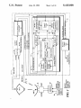
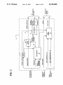
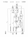
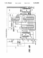
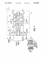
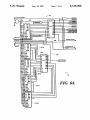
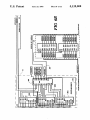
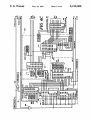
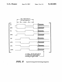
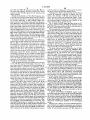
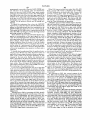
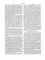
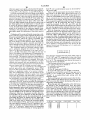
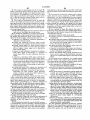
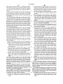
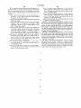
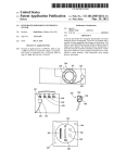
llllllllllllllllllllllIllllIlllllllllllllllllllllllllllllllllllllllllllllll
USOO5125008A
United States Patent [19]
[11]
Patent Number:
Trawick et al.
[45]
Date of Patent:
5,125,008
Jun. 23, 1992
METHOD AND APPARATUS FOR
Improves Antenna Range Productivity“, Microwave
AUTORANGING, QUADRATURE SIGNAL
Journal, Mar. 1989. vol. 32, No. 3, pp. 163-170.
GENERATION, DIGITAL PHASE
REFERENCE, AND CALIBRATION IN A
HIGH SPEED RF MEASUREMENT
RECEIVER
Churchill et al.. “The Correction of] and Q Errors in a
[75] Inventors: Charles D. Trawick, Tucker; Owen
M. Caldwell, Dunwoody, both of Ga.
Operating and Service Manual for the HP8510 Net
work Analyzer, pp. 8-275/8-276, pp. 8-241/8-242
(date unknown, but more than one year before ?ling
[73] Assignee: Scienti?c-Atlanta, Inc., Atlanta, Ga.
[21] Appl. No.: 491,186
date hereof).
[54]
[22] Filed:
[51]
[52]
Coherent Processor", IEEE Trans. Aerospace and
Electronic Systems, vol. AES-l7, No. 1(Jan. 1981), pp.
131-137.
Maintenance Manual for the Scienti?c Atlanta Series
1780 Programmable Microwave Receiver, Part I
(1984), pp. 44554-90.
Mar. 9, 1990
Oliver and Cage, “Chopper Ampli?ers", Electronic
Int. Cl.5 ............................................. .. H04B 1/10
13.5. CI. .................................... .. 375/102; 375/39;
Measurements and
[58]
Field of Search ..................... .. 375/39, 98, 102, 7,
Primary Examiner—Stephen Chin
375/8, 10, 106; 455/234. 304; 329/320; 324/76,
Anorney, Agent. or Firm—Jones, Askew & Lunsford
77 R
[56]
[57]
ABSTRACT
Improved autoranging, calibration, and complex signal
References Cited
U.S. PATENT DOCUMENTS
3,950.750
4/1976
Churchill et a]. ..................... .. 343/5
4.464.723
8/1984
9/1989
Chartier ....... ..
4,864,244
4,926.443
5/1990
Reich
detection circuits for an intermediate frequency (IF)
stage in a radio frequency (RF) measurement receiver.
An improved autoranging circuit sets a gain stage of a
375/98
Sasaki .... ..
selectively variable gain ampli?er prior to each data
acquisition cycle, to provide for wide dynamic range
375/39
..........
Instrumentation, pp. 204-209,
McGraw-Hill Book Company (1971).
375/98
. . ..
375/39
4,980,648 12/1990
Jaeger et al. ..... ..
325/98
4.991.164
2/1991
Casiraghi et a1. ..
375/98
4,991.184
2/1991
Hashimoto ............................ .. 375/8
and rapid time domain response. An improved complex
signal detection circuit for generating an inphase (I) and
quadrature phase (Q) signal from an input IF signal in a
OTHER PUBLICATIONS
signal channel and a reference channel is constructed
with a novel commutating demodulator circuit. Cali
Jung et al., “Modem-Circuit Techniques Simplify In
strumentation Designs“. Electronic Design News. vol.
29, No. 16, Aug. 9, 1984, pp. 165-176, 178. (Abstract
bration is effected with an improved digital phase refer
ence method and apparatus wherein effectivr 90° phase
shifts are digitially generated by shifting the generation
sequence of timing signals for the complex signal detec
only).
Scienti?c Atlanta. description of Scienti?c-Atlanta
Series 1780 programmable Microwave Receiver, “An
tion circuit instead of phase shifting a known calibration
tenna and RCS Instrumentation Products", 1990, pp.
signal, obviating the need for precision phase shifters,
38-50.
Scienti?c Atlanta, description ofthe Model 1795 micro
Doppler frequency generators, or Fourier transforms to
obtain correction components for the optimum detec
wave receiver, “Antenna and RCS Instrumentation
tion of complex signals.
Products", 1990, pp. 51-55.
Scienti?c-Atlanta, “Highspeed Measurement Receiver
51 Claims, 11 Drawing Sheets
.
_
1
1
LOCALOSCILLMUR
j
woman
link" 11
kn 11
g
5
xurr
1
1
"0112
v5“
n
111-
T
‘
3S
:
1
"M"
_
t
D
1516mm" ;
L'—1
011m Flwwnq Cam‘:
,m,: .... “16.1mm...
I
g
1211/1201
,'
“\ Oz/Amp
1
1
z
‘5
; 11'; (arr 011M111
3
z
-
f
;
(‘Jl?rul
;
;
‘mm;
.
L5
;
1
W
12b:
;
i
.
1:" Dumrl) ‘
'
__
cannot
'
;
I
:
m‘
I
RFSMTFH
z
1
'
_ m}\ Alllllnl‘l‘znb
01111111111111
XMITR
:
1
;
um
‘
ummr
P
:
:
Dtmnduuhv - .
—<
[
10m cuocxl
4*‘
f
I
45.1
I
'
1
I
“
45 mmr In“;
I
’"\
1
1
I, :
1
[
:
29
I
1
IFPROGSSORUNH'
. ...........................................
I
SWITDI
:I
I
ISMMSIGNALCNANNEL
i
B
1_.
45mm
REFCHANNEL
l0 MHz c0110
I
1
.
;1
manner
'
'
-
;
.
In
(5“; (1,111.41) :2
z
:
I
,
"""""""""" "
1
51,111
1
I
51111.1
I
I
‘mm’
Bun Dngnm-
I
Ram“
I
1
C‘J'M
£11
Amznm Tm
1
Awhai-n
1
DATA Qt rr
__
1r DIGITAL mu
,
FIBER oimc CONTROL
\
'
I
:5
:
US. Patent
June 23, 1992
Sheet 4 of 11
5,125,008
m‘0OhESQEOE<25%
2?WI_
s.imz€
US. Patent
June 23, 1992
Sheet 6 of 11
5,125,008
US. Patent
June 23,1992
Sheet 7 of 11
~
5,125,008
r50
PHASE WALK
lNTEGRATE
2 5% 8 9
‘@122@32 9
0I5)
1514
US. Patent
June 23, 1992
‘.3 g
SE:
g
8 8
Sheet 9 of 11
88
5,125,008
2
E g 88888888
LL‘ 9 8688588E8§
SCG'IOAUFDENG
88888888
3888888888 g
|| 88888888
OF“
J! 22291822222222
g 858868888é
E88888888
i E
—
85388
__ V
6888 l
J
g
_
US. Patent
June 23, 1992
'
:‘
Sheet 11 of 11
5,125,008
Any 1011s interval
during integration
i
1% WW
IN WW
INS MW
Q?
_1——\
rim
QNS
QN
At 180 p.s, IP=IN=QP=QN=0
and IPS=1NS=QPS=QNS=1
resulting in signal "hold"
F6, 8
Typical Timing Interval During Integration
1
5,125,008
2
range may be compromised in exchange for speed.
METHOD AND APPARATUS FOR
Also, receivers require interfacing to other measure
AUTORANGING, QUADRATURE SIGNAL
GENERATION, DIGITAL PHASE REFERENCE,
ment subsystems to produce outputs such as antenna
radiation patterns.
Particular problems have been encountered in the
design of measurement receivers which provide an
AND CALIBRATION IN A HIGH SPEED RF
MEASUREMENT RECEIVER
acceptable response time, frequency agility, and dy
TECHNICAL FIELD
The present invention relates generally to radio fre
namic range. For example, it is known that the signal
level can suddently change in a measurement environ
ment, as when the transmit antenna‘s polarization shifts
quency (RF) receivers, and relates more particularly to
from horizontal to vertical polarization. The sudden
signal level change can result in overranging of the
circuitry and inaccurate measurements unless the dy
improvements for the intermediate frequency (IF)
stages in a RF measurement receiver particularly useful
for measuring the RF and microwave performance
characteristics of antennas, components and materials.
namic range and response time are sufficient to handle
BACKGROUND
the change and can change quickly enough to preserve
the measurement opportunity.
One known method for adapting to signal level
Modern microwave radar and communication sys
tems rely heavily on the performance characteristics of
antennas. Continuing advancements in antenna design
changes may be referred to as the "dual-cycle" auto
ranging approach. In this method, the signal level from
have resulted in improvements in these systems and
have challenged instrumentation manufacturers to pro
the previous cycle is used to set the gain level for a
current cycle. This approach has the inherent disadvan
tage that there is risk of loss of data if the signal level
vide instruments that can accurately measure the per
formance characteristics of new antenna designs, such
changes abruptly between measurement cycles.
To avoid the latency resultant in dual-cycle autorang
ing, another known autoranging approach sets the gain
as multibeam antennas, electronically steered phased
arrays, dual-polarized and shaped-beam re?ectors, and
low sidelobe and broadband omnidirectional antennas.
Antenna testing is a multidemensional measurement
stage for each measurement cycle based upon the in
coming signal level. This method, which may be termed
problem. The received signal from an antenna under
test (“AUT") is a phasor quantity. It is a function of the
antenna‘s frequency, beam position for steered-beam
arrays, polarization, spatial position (such as azimuth
the “long-cycle" approach, involves lengthening the
30
and elevation angles), and other parameters. The re
ceived signal's amplitude and phase components are
principal parameters of operation which are recorded as
a function of position and other pertinent test parame
ters such as frequency and polarization.
It is believed that improvements in antenna range
productivity may best be achieved by enhancing re
ceiver performance characteristics. The major receiver
measurement cycle to allow for settling of the signals
through the circuitry. Thus, this method has the disad
vantage that the measurement cycle is necessarily
lengthened, which affects overall measurement speed
and bandwidth.
Calibration of measurement receivers is also of a
critical importance in antenna testing. Calibration of a
receiver entails providing a reference signal (which
may originate in a local oscillator unit associated with a
test range), typically at full scale and at a known phase,
and measuring the effect which the various circuits in
characteristics affecting antenna measurements include
the receiver may have on the reference signal. Correc
tions for detected errors are then provided. During
measurement speed, frequency agility (the ability to
change frequencies rapidly); dynamic range, interface
calibration, the reference signal is typically imposed
compatibilities with computer~controlled systems, the
The time required to take an individual measurement
is governed primarily by a measurement receiver's ac
upon both the signal channel and the reference channel
of the receiver, both of which must be independently
calibrated. In addition to measuring gain effects, the
phase of the signals in both channels must be measured
quisition speed. Measurement speed is the the rate at
and corrected, if necessary, so as to cause measurement
number of measurement channels, and remote control
capability.
45
values during operation to be expressed relative to a
matted data. The apparent speed of many conventional 50 calibrated signal. Often, measurement values are ex
pressed in complex signal form, with an inphase compo
receivers is usually fast enough that the measurement
nent (I) and a quadrature component (Q), which are 90°
processing time is transparent to an operator. However,
out of phase with respect to each other.
actual receiver speed becomes apparent when repetitive
In particular, three error types typically occur in
tasks are performed, such as in multifrequency or mul
tiported measurements wherein the frequency can be 55 phase/amplitude measurement receivers utilizing com
which a receiver can acquire, process, and output for
changed more rapidly than measurements can be pro
cessed and provided as outputs.
plex signal detection circuits: (1) offset errors, that is,
Fast, coherent, wideband measurements require that
quadrature outputs of the receiver channel, (2) orthogo
nality errors, that is, deviation of the inphase and quad
a receiver remain phase-locked to the transmit source at
fixed values which must be added to the inphase or
all times. A receiver’s frequency agility characterizes its 60 rature reference signals from being exactly 90° out of
phase with respect to each other, or deviation of the
ability to maintain phase-lock when encountering rapid
phase shifts in the inphase and quadrature sides of the
frequency transitions.
demodulator from each other, and (3) gain errors, that
Receivers must also provide sufficient dynamic range
is, a discrepancy in the gain of the inphase signal path as
for the required measurement accuracy. Current ultra
low sidelobe antennas have sidelobes in the —60 dB 65 compared to the quadrature signal path.
In one known prior art approach to the calibration
range, which may require a dynamic range of 80 dB or
problem for a complex signal measurement circuit, US.
more for acceptable accuracy. When measurement
Pat. No. 3,950,750 to Churchill et al., a calibration refer
speed is an overriding factor, the receiver's dynamic
3
5,125,008
4
previous output fed back from a holding register and
ence signal is generated with a slight frequency offset,
causing its phase to continuously vary during the cali
bration process. The phasor output of the complex sig
nal circuit is sampled at appropriate intervals, and a fast
the absolute value of the new output from the A/D
flash converter. After a predetermined number of sam
ples is accumulated. an autorange decision based on the
Fourier transform (FFT) is performed on the resulting
number presented by the holding register is made. The
data. The result of the FFT is used to generate correc
integration interval may be either a half-cycle or a full
tion coefficients for application to signals passing
through the complex signal circuit. However, this ap
proach relies upon precise timing of the samples with
integration of the absolute value for either one half or
cycle ofthe signal frequency (nominally 100 kHz). The
one full cycle of the signal frequency makes the result
respect to the phase of the frequency offset reference H 0 independent of the incoming signal‘s phase or of the
signal, plus the added computational complexity atten
starting time of the measurement.
dant to the FFT algorithm.
Brie?y described, the improved digital phase refer
Another similar prior art approach eliminates the
ence circuit and method of the present invention allows
timing constraints by using switchable phase shifting
for improved calibration of a complex signal detection
elements within a calibration reference signal generator. 5 circuit, to correct for offset, gain, and orthogonality
However, this technique relies heavily upon the preci
sion and constancy ofthe phase shifting hardware. Con
trollable phase shifts of the precision required for accu
errors. The invention comprises means responsive to a
cations applications, namely, in methods for calibration,
complex signal generation, autoranging. and the like, at
generates timing signals for causing the complex signal
calibration command for generating an IF (nominally
45 MHz) calibration reference signal. The calibration
rate antenna measurement applications are difficult and
reference signal is provided as the input signal to the IF
20
expensive to achieve.
stage, and thence (after downconversion) to the com
Accordingly, there is still need for further improve
plex signal detection circuit later in the IF stage, instead
ments in radio frequency receivers used in radar, an‘
of as an RF signal to the front end of the receiver. Tim
tenna. components. and materials testing. and communi
ing signal means, a ROM in the disclosed embodiment,
detection circuit (a commutating demodulator in the
lower cost but with improved performance.
preferred embodiment) to convert the input signal into
an inphase output signal and a quadrature output signal.
SUMMARY OF THE INVENTION
A phase offset signal means responsive to the calibra
Briefly described, the present invention comprises
improvements in the intermediate frequency (IF) stages 30 tion command provides a phase offset signal corre
sponding to a predetermined “effective" phase offset
ofa radio frequency measurement receiver including a
for the calibration reference signal. The phase offsets
novel complex signal demodulator circuit and method,
are
preferably generated for effective phase shifts of O",
an improved autoranging circuit and method for pro
90“, 180°, and 270°.
viding rapid response over a wide dynamic range. an
Timing signal altering means responsive to the phase
improved digital phase reference apparatus and method
offset signal alters the timing of the timing signals for
which facilitates calibration of the receiver by shifting
the complex signal detection circuit so that the complex
the phase of the reference signal used in the demodula
signal detection circuit provides phase-offset inphase
tor instead of providing a phase shifter at the front end
of the system, and improvements in the topology of a
and quadrature phase output signals which are shifted in
phase by an effective amount corresponding to the pre
commutating demodulator which results in a more
compact yet still precise circuit design.
More particularly described. the autoranging method
and apparatus ofthe present invention comprises a digi
tal autoranging circuit including a flash analog-to-digi
tal (A/D) converter which produces digital samples of
determined phase offset. The timing signal alteration is
effected digitally and completely within the timing
signal ROM, by providing the phase offset signal as
additional address inputs to the ROM corresponding to
45 a set of predetermined phase offsets.
the input signal, an adder/accumulator which accumu
lates the absolute value of the digital samples, means
responsive to the accumulated absolute value of the
samples during an accumulation cycle, means for select
ing a gain range for the input signal as a result of the 50
accumulation cycle through selectivety variable gain
stages, prior to providing the autoranged signal to sub
phaseooffset inphase and quadrature phase output sig
nals generated during calibration.
detection circuit also stores a plurality of sets of timing
signal level information from one measurement cycle is
used to set the input sensitivity for the next cycle. The
signals, which are selected by the phase offsets. Each of
the sets of timing signals are effectively phase-shifted
with respect to a master cycle time, synchronized to the
input IF signal, so that the complex signal detection
circuit effectively shifts its operation in phase by an
amount corresponding to a selected phase offset. In
present invention therefore overcomes limitations on
latency imposed by the prior art dual'cycle approach,
and permits potentially higher measurement speeds and
response to changes in signal level than the prior art
long-cycle approach, without losing data when the
input level changes abruptly between measurement
order to calibrate the receiver, a predetermined set of
cycles.
variations in the "effective phase“ of the timing signals
stored in the ROM are provided during a calibration
Still more particularly described, the improved auto
tables used to integrate the absolute value of the incom
ing signal. The output of the ROM is the sum of the
for I and Q signals provided from the complex signal
detection circuit, based on corrections derived from the
ory for storing the timing signals for the complex signal
the known dual-cycle type of autoranging in which
a read only memory (ROM) containing look-up math
lates a calibration correction for gain and orthogonality
Stated in other words, the ROM utilized as the mem
sequent signal processing stages. This approach avoids
ranging circuit provides for digital integration utilizing
After conversion to digital form, external means such
as a microprocessor associated with the receiver calcu
65
operation. Calibration is then effected by measuring the
known calibration reference signal which originates in a
local oscillator unit associated with the receiver and
measuring the effect of the various switchable gain
5
5,125,008
6
stages used in autoranging on this reference signal, as
ing node, while a second switching means responsive to
.modi?ed by the various phase offsets.
the negative switching signal switches an inverted input
signal to the integrating node 180° later in the cycle.
Third switching means responsive to the positive shunt
signal holds the input of the first switching means close
to ground during the switching signal, while a fourth
switching means responsive to the negative shunt signal
holds the input of the second switching means close to
A correction matrix is then computed for each state
ofthe switchable gain stage, which, when multiplied by
subsequent inphase and quadrature phase values, will
remove the measured phase, orthogonality, and gain
errors from the measurements. These matrix computa
tions are preferably carried out in a digital signal pro
cessor associated with the receiver's control unit. The
ground during the switching signal. A synchronizing
resulting corrected signals have a phase and amplitude
latch synchronizes all timing signals to the clock signal,
which are referenced to the phase and amplitude of the
which, it will be recalled, provides a stable phase refer
full-scale calibration reference signal.
ence.
The present invention thereby provides means for
Accordingly, it is an, object of the present invention
correcting offset errors, that is, ?xed values added to
to provide an improved high speed RF measurement
the inphase and quadrature phase outputs of the re 5 receiver for complex signals.
ceiver channel, and for correcting orthogonality errors.
It is another object of the present invention to pro
(Inphase and quadrature offsets are corrected before the
vide an improved calibration method and apparatus for
matrix multiplications, and do not vary with gain
radio frequency receivers, to allow correction of offset,
switching.) Those skilled in the art will appreciate that
gain, and orthogonality errors.
the known prior art calibration methods which involve
It is another object of the present invention to pro
phase-shifting and frequency shifting an RF calibration
vide an improved commutating demodulator circuit
signal at the front end of the system during calibration,
topology which exhibits reduced output errors.
followed by FFT to extract the needed correction
It is another object of the present invention to pro
terms, are obviated, in that the present invention pro
vide an improved topology for a commutating demodu
vides means for effectively shifting the calibration refer 25
lator which results in reduced parts count while still
ence signal through phase offsets, with the results being
avoiding errors which would have arisen had additional
.
combined to correct for all known error terms.
buffering of phase referenced demodulator timing sig
Brie?y described, the preferred invention further
nals been necessary.
relates to an improved commutating demodulator to
pology which is very exacting and provides demodula
30
tion operation more precise than prior art demodula
tors. The improved demodulator topology comprises
memory means for storing timing or control signals
It is another object of the present invention to pro
vide an improved autoranging method and apparatus
for use in RF and microwave measurement receivers
which permits higher response speeds to dynamic com
plex signals without sacrificing dynamic range of the
complex signal detection circuit.
It is another object of the present invention to pro
(such as the ROM discussed above when the demodula
tor is used in a complex signal measurement applica
tion). synchronizing means for synchronizing the con
trol signals provided from the memory with an accurate
time reference, means for multiplying a phase reference
vide an improved autoranging method and apparatus
which allows adjustment to input level changes for each
signal by the signal to be demodulated by commutating
cycle of an input IF signal, by gain ranging prior to
output signal referenced to the phase ofa known phase
reference signal during a conversion cycle. A clock
times higher than the predetermined frequency of the
input signal. Locking means phase locks the clock sig
derive correction components.
It is another object of the present invention to pro
vide an improved digital phase reference method and
apparatus for a radio frequency measurement receiver,
which allows introduction of a periodic increment of
nal to the reference channel input signal. A counter
counts n cycles of the clock signal to de?ne a single
predetermined angular increment over a given time
switches. and means for directly driving the commutat 40 providing the input signal to subsequent processing.
It is another object of the present invention to pro
ing switches from the synchronizing means, thereby
vide an improved calibration method and apparatus for
avoiding further errors which would have arisen had
a radio frequency receiver which obviates the need for
additional buffering of the timing signals been required.
a precision phase shifter or a Doppler frequency genera
More particularly described, the improved commu
tating demodulator circuit is responsive to an input 45 tor at the front end or RF input of the receiver, and
obviates the need for a FFT or spectrum analysis to
signal at a predetermined frequency for providing an
means provides a clock signal having a frequency n
phase offset to cause the receiver to “phase walk" a
cycle of the input signal, allowing the control signals
cycle, so as to provide a novel measurement methodol
from the memory means to be synchronized with the 55 ogy.
These and other objects, features and advantages of
reference channel input signal. The control signals com
the present invention may be more clearly understood
and appreciated from a review of the following detailed
prise a positive switching signal, a negative switching
signal, a positive shunt signal, and a negative shunt
description of the disclosed embodiment and by refer
ence to the appended drawings and claims.
signal. The positive switching signal and the negative
switching signal are 180° out of phase with respect to
each other, and the positive shunt signal and the nega
tive shunt signal are 180° out of phase with respect to
each other. The positive shunt signal is always the logi
cal inverse of the positive switching signal, and the
negative shunt signal is always the logical inverse of the
negative switching signal.
A first switching means responsive to the positive
switching signal switches the input signal to an integrat
BRIEF DESCRIPTION OF THE DRAWING
FIGURES
FIG. 1 is a block diagram of a radio frequency re
65
ceiver which includes the preferred autoranging and
demodulator embodiments and a control/timing circuit
which includes the preferred digital phase reference
embodiment constructed in accordance with the pres
7
5,125,008
ent invention, utilized in an antenna test system con?gu
ration.
FIG. 2 is a block diagram of the preferred embodi
men'. of a control/timing circuit constructed in accor
dance with the present invention, which is utilized in
the receiver system shown in FIG. 1
FIG. 3 is a block diagram of the preferred embodi
8
Digital data corresponding to the phasor values of the
signal and reference channels are generated by a con
trol/timing circuit 15 in the IF processor 20 and sent as
the signal IF DIGITAL DATA to the receiver control
unit 22.
In FIG. 1, horizontal and vertical polarization an
tenna elements in the AUT provide a horizontally po
ment ofa 100 kHz autoranging circuit and commutating
larized input signal HORIZ and a vertically polarized
demodulator constructed in accordance with the pres
ent invention, which is utilized in both the signal chan
nel and the reference channel of the receiver system
shown in FIG. 1.
FIGS. 4 A and B is a detailed schematic diagram of
the autoranging circuit employed in the preferred em
input signal VERT to an RF switch 24, which switches
between the two polarized signals under control of a
bodiment of FIG. 1 and shown generally in FIG. 3.
FIG. 5 is a detailed schematic diagram of the im
proved commutating demodulator employed in the
preferred embodiment of FIG. 1 and shown generally
in FIG. 3.
FIGS. 6A-6C, is a detailed schematic diagram ofthe
signal RCVR RF SWITCH CONTROL provided by
the LO unit 21. The incoming signal from the switch 24
comprises a LO & IF SIGNAL provided to the LO unit
.21. The L0 unit 21 in the preferred embodiment may be
remotely located so as to preserve the sensitivity and
dynamic range features desired in antenna range instal
lations. Typically, a user of the system may elect to
place the LO unit 21 as close to the AUT as is practica
ble. The L0 unit 21 is controlled by a ?ber optic control
line 25 between a receiver control unit 22, allowing
separation up to 2000 feet between the LO unit and
other parts of the receiver.
control/timing circuit shown generally in FIG. 2.
FIG. 7 is a timing diagram illustrating the timing ofa
Also connected to the LO unit 21 is a reference an
typical data acquisition cycle carried out by the pre
tenna horn 26, which is typically positioned at a station
ferred embodiment of the present invention.
FIG. 8 is a timing diagram illustrating the timing ofa 25 ary location in the antenna range and which receives a
typical l0 its interval during the integration period in
constant reference signal from a transmitter antenna 28.
the data acquisition cycle shown in FIG. 7.
The signal from the reference antenna 26 is denomi
nated LO & IF REF which is provided to the LO unit
DETAILED DESCRIPTION OF THE
PREFERRED EMBODIMENT
Referring now to the drawings, in which like numer
21.
The transmit antenna 28 provides selectable horizon
tally and vertically polarized transmitted signals, de
nominated HORIZ and VERT, which are provided
from an RF switch 29. The receiver control unit 22
provides a signal XMITR RF SWITCH CONTROL
speed measurement receiver 8 which includes an im
proved second IF subsystem or circuit 10 constructed in 35 which switches between horizontal and vertical polar
izations to the transmitting element in the antenna 28,
accordance with the present invention. namely. an im
from a transmit signal source 30, typically an RF trans
proved 100 kHz autroranging and demodulator circuits
mitter ampli?er.
12a. 12b, and a control/timing circuit 15, which in
The primary function ofthe IF processor unit 20 is to
cludes the improved digital signal reference circuits and
facilitates the disclosed calibration method to be de 40 provide two stages of intermediate frequency process
ing for the receiver, so as to obtain a 100 kHz reference
scribed hereinbelow. The improved second IF subsys
signal channel REF from the reference horn 26 and a
tem 10 is included within an intermediate frequency
100 kHz signal channel SIG from the AUT. The LO
(IF) processing unit 20, which includes a number of
unit 21 provides outputs comprising a 45 MHz REF
other components including a ?rst IF subsystem 14
als indicate like elements throughout the several draw
ing ?gures, FIG. 1 shows a radio frequency (RF) high
which do not form a part of the present invention. The 45 CHANNEL, a 45 MHz SIGNAL CHANNEL, and a
coherent oscillator signal 10 MHz COHO to the IF
complete receiver 8 further includes a local oscillator
processor unit. Details ofthe LO unit 21 are not consid
(LO) unit 21 and a receiver control unit 22 which are
interconnected in the manner to be described.
ered part of the present invention, and will not be dis
cussed further herein, except to say that the preferred
By way of background, the receiver 8 is shown in
LO unit 21 need not include means for generating a
FIG. 1 connected to an antenna under test (AUT),
phase-variable or frequency-variable calibration signal,
which is typically mounted in an antenna testing range
for performance testing. The receiver 8 comprises a
because of the present inventions. However, it will be
understood that the LO unit 21 provides a constant
high speed, high accuracy, coherent A/D conversion
frequency calibration signal on both the 45 MHz REF
system for RF signals such as microwave signals. Co
herent detection results from providing completely 55 CHANNEL and the 45 MHz SIGNAL CHANNEL in
response to a calibration command provided from the
separate signal and reference channels that are phase
receiver control unit 22 via the ?ber optic control line
locked together. An LO unit 21 provides a local oscilla
25.
tor signal that ranges from 1.9 to 4.6 GHz in the pre
The IF processor unit 20 further comprises other
elements comprising a ?rst IF subsystem 14, not part of
?ed and buffered in the LO unit 21 and transmitted to an
the present invention, including an intermediate fre
quency reference generator 33, which divides down the
IF processor 20, where they are further ampli?ed and
coherent clock signal 10 MHz COHO provided from
downconverted to a second IF frequency of 100 KHz.
the LO unit and provides a precision stable time base 10
Then. the 100 kHz IF signals are autoranged, synchro
nously detected using an internal high stability time 65 MHz CLOCK signal to the control/timing circuit 15.
The IF reference signal generator 33 provides a
base as will hereinafter be described, transformed into
highly stable 100 kHz signal to an offset frequency
quadrature signals I and Q, and converted to digital
ferred embodiment, and provides a resulting ?rst IF
frequency of45 MHz. The 45 MHz IF signals are ampli'
format for utilization by a receiver control unit 22.
converter 35, which generates a 45.1 MHz signal that is
9
5,125,008
10
provided to 45 MHz IF downconverters 38a, 38b, for
the signal and reference channels, respectively, whose
outputs are the 100 kHz signals for the reference and
control unit do not form part of the present invention,
signal channels.
module 15 comprises a plurality of digital state ma
chines, state machine A 50 and state machine B 51,
Details of the operation of the offset frequency con
verter 35 will not be described further herein, inasmuch
as the same is described in copending application Ser.
No. 491,161, ?led Mar. 9, 1990, entitled "Offset Fre
quency Converter for Phase/Amplitude Data Measure
the same will not be discussed further herein.
Turning next to FIG. 2, the preferred control/timing
which provide timing and sequencing signals. These
timing and sequencing signals control analog process
ing, analog-to-digital conversion, and transfer of the
results to the receiver control unit 22.
ment Receivers“ and owned by the same assignee as the
The 10 MHz CLOCK signal provided from the IF
present invention, which is incorporated herein by ref
reference generator 33 is provided to through a clock
buffer 52 to the state machine A 50, the state machine B
51, and a phase reference circuit 55.
The state machine A circuit 50 is the primary control
ler for the data acquisition process. Upon arrival of a
erence and made a part hereof as if the same were set
forth fully herein. However, it should be understood
that the offset frequency converter is operative to pro
vide a 45.1 MHz signal to both downconverters 38a and
38b, which is phase locked to the 45 MHz REF CHAN
NEL, with a highly accurate 100 kHz frequency offset
added thereto, so that a highly accurate 100 kHz signal
will be provided by both downconverters 38 to the
TRIGGER signal from the receiver control unit 22,
state machine A ?ags that it is busy with a BUSY signal,
which is a status signal back to the receiver control unit
22. State machine A then sequences the 100 kHz de
20 modulator circuits 12a, 12b through a single data acqui
circuitry 10 of the present invention.
sition cycle. A typical data acquisition (or measure
It should be further understood that the differences
ment) cycle is shown and described more particularly in
between the 100 kHz signals from the downconverters
connection
with FIG. 7. In general, however, state
38a and 3812 are thus dynamically limited (i.e., within
machine A provides phase reference gating signals on
acceptable error tolerances) to the differences in phase
and amplitude between the reference signal and the 25 lines 58 to a phase reference circuit 55 and control sig
nals on lines 59 to the demodulators 12.
signal from the AUT, which re?ect the measured pa
The phase reference circuit 55 divides the 10 MHz
rameters of the AUT. This dynamic limitation, which
reference clock by 100 to generate TIMING SIG
results from the operation of the referenced copending
NALS on lines 57 for controlling FET switches in the
application, allows the present invention to operate
demodulators 12, and receives and stores a PHASE
successfully, inasmuch as the 10 MHz CLOCK signal
OFFSET signal from the receiver control unit 22. The
and the 100 kHz signals from the downconverters 38 are
phase locked. It will thus be understood that the preci
sion ofthe 100 kHz signal frequency is of importance to
phase reference circuit further includes means respon
sive to the PHASE OFFSET signal for effectively
shifting the phase of the timing signals on lines 57 dur
operation of the present invention, and contributes to 35 ing a calibration operation. As will be discussed fully
the high levels of accuracy obtainable.
After the signal and reference channels are converted
to the 100 kHz second intermediate frequency, they
enter the second IF subsystem 10 for autoranging, de
modulation (that is, conversion to baseband), integra
below, the phase offset is transformed by using a read
only memory (ROM), which allows the introduction of
an arbitrary phase shift for calibration purposes.
Still referring to FIG. 2, state machine B 51 controls
the transmission of digitized signals from A/D convert
tion, and analog-to-digital conversion. It will be appre
ers in the signal and reference channels to the control
ciated that the the present invention relates primarily to
unit 22 by sequentially enabling the data onto the output
the second IF subsystem 10. which comprises the con
buses DATA OUT and generating accompanying
trol/timing module 15 and the 100 kHz signal channel
strobes. State machine B is constructed separately from
and reference channel autoranging demodulators and 45 state machine A so that another data acquisition cycle
A/D converters 12a and 12b, which derived amplitude
can begin during transmission if required.
and phase data in the form ofI and Q digital output
State machine B 51 provides enable signals desig
signals, provided as IF DIGITAL DATA.
nated OUTPUT ENABLES on lines 61 to A/D con
The digital results are then transferred out of the IF
verters (see FIG. 3), and also controls data buffers 60.
processor unit 20 to the receiver control unit 22 for
The data buffers 60 receive the digitized signals denomi
further processing, display and output. The receiver
nated DATA (SIGNAL) I, Q and DATA (REFER
control unit 22 provides as outputs 5000 samples per
ENCE) I, Q from the A/D converters, and a GAIN
second for the signal and reference channel. Amplitude
CODE signal from the autoranging circuit 75 (see FIG.
and phase or I and Q outputs are provided in digital
3). The outputs of the data buffer 60 are the output
form as DATA OUT in a variety of ?oating point nu 55 signals DATA OUT, which are provided to the re
merical formats for further calculations and display.
ceiver control unit 22.
The receiver control unit 22 also provides controller
A GAIN STUFFING CONTROL signal is also
interfaces such as an IEEE-488 bus, RS232/449 serial
provided to the state machine A 50 and to the autorang
interfaces, a BCD recorder, and the like. The control
ing circuit 75 (FIG. 3). This signal, which originates in
unit utilizes high speed digital signal and ?oating point 60 the receiver control unit 22 to control the autoranging
processors to receive the raw data signals and apply
gain stages during calibration, controls the provision of
calibration corrections, numerical conversions, coher
a gain code indicative of the current gain setting of a
ent averaging, and normalizations in real time. The
selectively variable gain ampli?er tn the autoranging
resulting formatted data is available to a user directly
circuit.
from the control unit 22 via a fast parallel interface and 65
Turning now to FIG. 3, each ofthe 100 kHz demodu
is also distributed inside the control unit for display and
lators 12a, 12b is of similar construction, as is shown in
output via the 488 bus, serial, and BCD recorder inter
FIG. 3. The demodulator circuit 12 comprises an input
faces. Inasmuch as the details of the preferred receiver
buffer 70 which ‘boosts the input 100 kHz signal to a
1]
5,125,008
12
Corporation of Somerville, N.J.. provides digital sam~
suitable drive level for subsequent circuit stages. The
output ofthe input buffer 70 feeds a variable gain ampli
?er circuit 72 and signal conditioning circuit 71. The
signal conditioning circuit 71 nulls the offset of the
input buffer 70 with a signal OFFSET NULL, and also
provides a scaled and shifted version ofthe input signal
ples of the SCALED INPUT signal, which has been
offset via an offset introducing part of the signal condi
tioning circuit 71 to center the voltage swing. The A/D
converter 101 is enabled for constant operation.
The offset introducing part of circuit 71 comprises an
operational ampli?er 91, preferably a type 5127 or
equivalent, con?gured to receive the input signal at its
denominated SCALED INPUT to an autoranging‘cir
cuit 75.
inverting input from the buffer ampli?er 70, with feed
The autoranging circuit 75 samples the SCALED
INPUT signal and selects a gain in the variable gain 0 back from the output, and to receive a mid-range output
reference signal from the.RM terminal of the ?ash A/D
ampli?er 72 with a GAIN CONTROL signal to com
converter at its non-inverting input. Five volt zener
pensate for low level inputs and provide for operation
diodes D9, D10 provide protection at the input VIN of
over a wide dynamic range. It does this in 6 dB incre
ments up to a maximum gain of 24 dB. The gain
adjusted output of the variable gain ampli?er 72 is then
provided to a demodulator and integrator circuit 80,
5
the A/D 101, which is connected to the op amp 91
output. The op amp 91 therefore references the input
signal to the midpoint of the operational range of the
where it is coherently demodulated in response to the
TIMING SIGNALS on lines 57 into inphase (I) and
A/D ?ash converter.
quadrature (Q) components which are integrated for
absolute value of digital samples provided by the A/D
converter 101. Accumulation is preferably performed
for a full cycle of the signal being autoranged, resulting
the remainder of a measurement cycle.
As a measurement cycle ends, 16-bit analog-to-digital
An adder/accumulator circuit 102 accumulates the
(A/D) converters 82a, 82b, for the I and Q signals,
respectively. capture the outputs of the integrators and
in decreased sensitivity to DC offsets. A comparator
begin a conversion cycle. When the conversion is com
(PAL) 103 makes a ?nal autoranging decision based on
plete. the OUTPUT ENABLES signal on line 61 from
the control/timing module 15 (FIG. 2) gates the results
the accumulated value, and provides an output signal
GAIN CODE (a three-bit code) to the other circuits for
utilization as a part ofthe data stream, and provides ?ve
SELECT lines 105 to the variable gain ampli?er 72.
The preferred adder/accumulator 102 includes a read
onto a common buss for provision to the data buffers 60.
Turning next to FIG. 4, next will be described the
details of the autoranging circuit 75 for measuring the
signal level and providing selectably variable gain. The
preferred autoranging circuit 75 comprises a detector of
sufficient accuracy for digital implementation of auto
ranging, and is based upon a ?ash A/D converter 101.
implemented in the form of programmed logic array
only memory (ROM) 130, which is preferably a type
CY7C263 manufactured by Cypress Semiconductor of
San Jose, Calif, having thirteen address lines and eight
output lines. The ROM is programmed with all possible
input buffer ampli?er 70, and variable gain ampli?er 72v
mathematical combinations of a six-bit “sample" value
Prior to reaching the ?ash A/D circuit 101, the input 35 (from the A/D 101) and a seven-bit “accumulated"
value (from a register or latch 131) which represents the
signal at 100 kHz is buffered by ampli?er 70. The pre
results of digital integration over a number of cycles,
ferred input buffer ampli?er 70 comprises a type 5l47
say, ?fty. Thus, six ofthe address lines to the ROM 130
operational ampli?er 112. con?gured via feedback net
are provided from the A/D 101, while seven of the
work comprising resistor R14 and capacitor C13 with a
gain of IQ for ampli?cation. with an output on line 116 40 input lines are provided from the outputs of an eight-bit
comprising the buffered output, The noninverting input
of the ampli?er 112 is connected to the output of an
offset-nulling operational ampli?er 113. Op amp 113 is
latch 131, which serves as the “accumulator” register.
Thus, the output of the ROM 130 at any given time is
the sum of the previous output (fed back from the latch
131), and the absolute value of the new output from the
con?gured to receive the signal on line 116 from the
ampli?er 112 via a low pass ?lter network comprising l 45 A/D converter 101. For each ?ash conversion, the
absolute value of the signal is added to the accumulated
,uF capacitor C15 and 15K resistor R8, so that any DC
amount. Any carry bits, which are represented by the
drift on line 116 is detected and nulled by adjusting the
highest order bit of the ROM 130. are counted by a
reference level at the noninverting input of op amp 112.
carry bit counter 132, which is clocked by a master 10
The variable gain ampli?er 72 comprises a plurality
of staggered value precision resistors Rl5‘R19 in series
and RIO-R13 to ground, which are switched to a com
MHz clock signal MClock. A control signal IF2
ACCUM provided from the state machine A 50 (FIG.
6A) clears the accumulated value in the carry counter
mon node 119 by ?ve analog switches 120, all of type
132 and latch 131, and is synchronized to a measure
CDG309 manufactured by Siliconix, Inc., of Santa
ment cycle.
Clara, Calif. The outputs of all analog switches 120 are
commonly connected at node 119 to the inverting input 55
After a predetermined number of samples is accumu
lated, preferably at least ?fty in the preferred embodi
of an operational ampli?er 112, whose output is fed
ment given the clock rate of 10 MHz and the IF fre
back through a precision resistor R20 to the inverting
quency of 100 kHz, the PAL 103 enacts an autoranging
input node, and whose noninverting input is referenced
ground. The combination of feedback resistor R20 and
decision based on the number provided to it from the
selectable input resistor networks Rl5-R19 in series and
counter 132 and latch 131. It should be understood,
RIO-R13 provide ?ve selectable gains: nominally 0 dB,
however, that the accumulation interval is preferably
chosen to be a full cycle ofthe signal frequency, namely
100 kHz, which permits 100 cycles of accumulation of
122 swings 10 VW and comprises the intermediate fre
the SCALED INPUT signal. Only the higher order of
quency 100 kHz autoranged signal denominated AU
TORANGED IF, which is provided to the demodula 65 signi?cance bits AC5~AC10 from the latch 131 and
6 dB, 12 dB, 18 dB or 24 dB. The output ofthe op amp
tors 12.
counter 132 are provided as address inputs to the PAL
The ?ash A/D converter 101, preferably a type
CA3306CE six bit converter manufactured by RCA
by Cypress Semiconductor of San Jose, Calif, which is
103. PAL 103 is preferably a type 22Vl0 manufactured
13
5,125,008
14
Other PAL inputs include four output lines QA-QD
programmed to provide a three-bit GAIN CODE out
put indicative of the selected value (or alternatively
from a counter 141, which is clocked by the IQ MHz
receive a three bit GAIN CODE input under certain
CLOCK buffered by the clock buffer 520. Counter 14]
conditions, described below) and ?ve bits of SELECT
provides various delay states of varying lengths. A
lines 105 to select one of the selectable gain stages ofthe
terminal count (TC) signal denominated PH TC from a
ampli?er 72. A “gain stuff‘ signal GSTUFF is provided
divide-by-IOO counter 142 (FIG. 6C) signals the end of
each cycle ofthe 100 kHz signal. The counters 141, 142,
151, 161 are all preferably type 74ALSI61 manufac
tured by Texas Instruments or equivalent.
A RESET signal provides another input to the PAL
as an input to the PAL 103, and determines whether the
autoranging result sets the gain or whether the gain is
“stuffed" by the receiver control unit 22 (during cali
bration).
It should be understood that when the GSTUFF
signal is true, a three bit value for GAIN CODE will be
present on the bidirectional data lines connected to the
140, and constitutes a master reset signal generated on
system powerup. Signals denominated GAIN STUFF
are provided to the PAL from a gain code stuffing
circuit 145 (FIG. 6C), which is operative to insert the
GAIN CODE lines, from the receiver control unit 22.
This causes the PAL 103 to select a particular one ofthe 5 three-bit GAIN CODE determined by the receiver
control unit 22 during calibration. The GAIN STUFF
select lines 105 to set the gain, thereby allowing external
signals comprise clock-synchronized versions of the
gain stage setting for calibration.
Those skilled in the art will understand that the inte
status signals GSTUFF, REF STF INV, and GAINl.
gration or accumulation of the input signal for a full
During normal operation. the gain code originates in
cycle for autoranging decision purposes will not vary
with signal phase or as the starting time for the accumu
lation changes, which thereby removes some difficult
timing constraints from the system. It will be further
the autoranging circuit 75 and passes to the receiver
control unit 22 via status latch 163, During calibration,
however, the receiver control unit 22 must force vari
ous gain conditions. It does so by means of control latch
understood that while a shorter integration interval. say
on the order of 5 microseconds (a half-cycle integra
tion) will also be operative, it has been determined that
a full-cycle integration is less sensitive to offsets and is
of a 200 115 acquisition cycle, and buffer 173 which is
turned on during the stuf?ng process to drive the gain
code lines as commanded by the receiver control unit
172 which samples the control signals at the beginning
preferred.
22. The GAIN] signal relates to a gain control circuit
(not shown) in parts of the IF processor unit 20 prior to
the circuitry 10 of the present invention.
A ?nal input to the PAL 140 in FIG. 6A is the signal
PH WALK EN, which signi?es "phase walk enable“.
This signal is asserted by the receiver control unit 22 to
It should also be understood that the preferred auto
ranging circuit 75 does not utilize the known prior art
approach wherein range information from one measure
ment cycle is used to set the input sensitivity or gain
ranging for the next cycle. Rather, the limitations on
signify that phase walking is desired. Phase walking
enables a pulse swallowing gate 146 (FIG. 6C) via the
latency imposed by the prior art approach are not pres
ent, so that higher speeds Of Operation are possible even
if the input level changes abruptly between measure
ment cycles. Thus, the signal AUTORANGED IF is
gain-ranged, indicated by the GAIN CODE, and ready
for processing at the appropriate time.
signal PHASE WALK, which blocks a single I00 nano
second pulse of the I0 MHz clock. The absence of a
single pulse from the clocking of the divide-by-IOO
counter 142 generates an effective 3.6“ phase offset or
shift in the operation of the demodulator circuit 80
It will now be appreciated that the use of the ?ash
(FIG. 5) in the autoranging demodulator 12, by post
poning the generation of the FET timing signals for one
clock cycle.
A/D converter 101 and digital accumulator 102 pro
vide speed and precision with minimal need for circuit
adjustments, while also providing rapid response time
with good noise rejection. It will be further appreciated
that the above-described approach separates the auto
Still referring to FIG. 6A, control outputs of the
PAL 140 include the BUSY signal, which is provided to
range measurement process from the main measurement
or digitization process. While the use of range selection
the receiver control unit 22 to indicate that a data acqui
sition cycle is in process. An IRESET signal causes
circuitry separate from main signal paths is known in
reset of the integrator circuits in the demodulator 80. A
the art, it is believed that the use of the ?ash A/D con
IF2 CKEN signal enables the clock at PAL 103 (FIG.
4). An IF2 ACCUM signal clears the accumulator 102.
These signals together control the autoranging process
by switching the clock to the accumulator 102 and
commanding the PAL 103 to apply the result to the
verter 101 to convert the input signal into a stream of
digital samples and to utilize such samples after accumu
lation and integration, provides novel advantages not
heretofore known. Primarily, it will be appreciated that
the autoranging method is carried out before the subject
signal is "detected", that is, the data is converted into
digital form.
Turning next to FIG. 6, consisting of FIGS. 6A-6C,
the control/timing circuit 15 controls many of the oper
ations of the demodulator and data conversion pro
cesses. Turning ?rst to FIG. 6A, the preferred control/
45
gain switches 120 (FIG. 4).
The state machine A 50in FIG. 6A further comprises
a second PAL 148, whose inputs are connected to four
cascaded counters 1Sla—15ld, all type 74ALSI6I,
which are clocked by the 10 MHz clock signal through
clock buffer v52a. The counters 151 are cleared when the
BUSY signal goes low (indicating not busy), and serve
as a time keeper during the 1800 clock cycles which
comprise a conversion cycle. At appropriate times dur
structed around a programmed logic array (or PAL)
ing the conversion cycle, PAL 148 provides a count
140 which receives various commands, status, and state
inputs and provides control outputs. The principal input 65 enable signal on line 152 to counter 141, advancing the
state machine A to its next state. These states are listed
is the TRIGGER signal from the receiver control unit
as a part of FIG. 7. PAL 148 also provides a MID
22, which is provided to one ofthe PAL 140 inputs. The
GATE output signal to flag the midpoint of the signal
TRIGGER signal starts a conversion cycle.
timing circuit 15 and its state machine A 50 is con
15
5,125,008
16
integration process. This signal goes through the re
described in more detail in connection with FIG. 5. The
ceiver control unit 22 and is available to the user.
preferred ROM 171 is a type CY7C263 manufactured
A principal output signal from the PAL 140 is the
INTEGRATE signal, which is true during the portion
of the conversion cycle and demodulation cycle for
integration by the demodulator 80. The INTEGRATE
signal controls the demodulator control signal memory
171 for demodulation (and integration) or hold (during
A/D conversion of the result). Signals denominated
HIGH GAIN SIG, HIGH GAIN REF, and IFl PK
by Cypress Semiconductor, and is 8K by 8. As dis.
cussed, five bits of input are provided from the phase
STB from PAL 140 control a switchable gain stage
located in the (45 MHz) ?rst IF subsystem 14 of the
receiver (FIG. 1), which does not form a part of the
offset latch 170, seven bits are provided from the divide
by-IOO counter 142, which counts cycles ofthe 10 MHz
clock to subdivide each IO us cycle of the 100 kHz IF
into 100 intervals of I00 nanoseconds (ns) each. The
remaining bit is the INTEGRATE signal, which con
trols the ROM for demodulation or hold.
The output signals from the ROM 171 comprise tim
ing signals on lines 57 for switching the FETs in the
demodulator 80 in FIG. 5, denominated QNS, QN,
age of a single clock cycle at the divide-by-IOO counter
QPS, QP, INS, IN, IPS, and IP, where Q signi?es the
quadrature channel, I signi?es the inphase channel, P
signi?es during the positive portion of the input signal,
N signi?es during the negative portion of the input
142 (FIG. 6C).
signal, and S signi?es shunt. as will be discussed more
present invention.
The PHASE WALK signal from PAL 140 is pro
vided to the pulse swallowing gate 146. to cause block
A LD STATUS REG signal from PAL 140 is pro
vided to a status register 163, to strobe data into the 2O
register.
In FIG. 6B. it will be seen that the state machine B 51
is constructed around a PAL 160. again a type 22Vl0.
The inputs to the PAL 160 include the RESET SIG‘v
fully below.
A gain code stuf?ng circuit 145 comprises a type
74LS374 latch 172, which is clocked by the BUSY
signal which clocks in the three-bit GAIN CODE from
the receiver control unit 22, denominated GAIN 0GAIN 2, and plus control signals REF STF INV,
NAL. the INTEGRATE SIGNAL, and timing signals 25 GSTUFF, and GAINI, which comprise the GAIN
STUFF signals. These signals allow the receiver con
generated by three cascaded counters 1610-161c, which
trol unit 22 to dictate the gain during calibration.
are clocked by the 10 MHz CLOCK and cleared on the
count of 400 with a signal on line 162 from one of the
output pins of the PAL 160.
As discussed above. the state machine B 51 controls
the gating of the data buffer 60. which comprises a pair
of type 74LS244 tristate eight-bit buffers manufactured
by Texas Instruments. These buffers 60 have their in
puts connected to the outputs of the analog-to-digital
The outputs of the latch 172 are provided as the
GAIN STUFF signals which signify the gain code
being provided for the reference channel or the signal
channel, and the I and Q portions thereof (again de
pending on timing), and are also provided to a tri-state
buffer 173, a type 74LS244. During calibration, the
outputs of the buffer 173 are enabled onto gain code
converters 82a. 82b (discussed in connection with FIG. 35 lines denominated REFO~REF2 and SlGO-SIG2.
These signals go to the reference and signal channel
3) on lines ADCO-ADCIS. and provide 16 bits of out
demodulators 12a and 12b respectively, where they are
put on lines DATAO-DATAIS to the receiver control
unit 22. A signal on line 164 from the PAL 160 enables
connected to the GAIN CODE pins of PAL 103 (see
FIG. 4). During normal operation, buffer 173 is disabled
the buffers 160 to place their signals onto a data bus
and PAL 103 provides the GAIN CODE signal for
DATA OUT, comprising signals DATAO~DATAI5.
transmission to the receiver control unit 22.
A STROBE signal is provided from the PAL 160 to the
Turning now to FIG. 5, the demodulator and integra
receiver control unit 22 to indicate that the data on the
tor circuit 80 of the 100 kHz demodulator 12 comprises
DATA OUT lines should be strobed in.
an improvied commutating demodulator which gener
Four output lines of the PAL 160 provide output
enable signals for the l and Q of the reference channel 45 ates I and Q output signals from the input signal AUTO
RANGED IF from the autoranging circuit 75 (FIG. 4),
and the I and Q ofthe signal channel, denominated REF
both phase-referenced to the 10 MHz clock as divided
Q OE. REF I OE. SIG Q OE, and SIG I OE. These
down by phase reference counter 142. The AUTO
signals sequentially enable the outputs of the A/D con
RANGED IF signal is provided ?rst to a unity gain
verters to be provided to the inputs of the buffer 60.
buffer comprising operational ampli?er 181, again a
A ?nal output from the PAL 160 is the line STATUS
type 5127. In addition, AUTORANGED IF is pro
OE, which enables the output of the status register 163
vided to a unity gain inverter comprising operational
to the data line DATA OUT, shown in FIG. 6C. The
ampli?er 182 connected in an inverting con?guration.
status register 163 is a type 74LS374, which stores vari
The op amp 182 provides a positive signal during nega
ous status information including the three-bit GAIN
CODE in the signal channel and the three-bit GAIN 55 tive excursions of the input signal, and a negative signal
during positive excursions of the input signal.
CODE in the reference channel, denominated SIG
The demodulator 80 comprises I channel 184 and Q
O-SIGZ and REFO—REF2, respectively.
channel 185, which are of similar construction except
In FIG. 6C, the control/timing circuit 15 further
they are clocked 90° apart by their respective timing
comprises a phase offset latch 170, preferably a type
signals. Referring particularly to the I channel 184, the
74LS374 manufactured by Texas Instruments. This
circuit includes a node 186 which is always held at
latch is clocked by the BUSY signal, which clocks in a
virtual ground by an integrator 200. The demodulator
5-bit phase offset number on lines PHASE O-PHASE 4,
operates by switching current proportional to the mag
which signify a desired phase offset provided for the
nitude of the input signal into this node.
calibration from the receiver control unit 22. The out
An L-topology switching network comprising a
puts of the phase offset latch 170 are connected to a 65
shunt ?eld-effect transistor (FET) 190 and a signal pass
timing signal ROM 171, which comprises the timing
ing FET 191 is connected to shunt the signal to ground
signal generator for the demodulator and integrator
or to the node 186, depending upon the timing signals.
circuit 80, part of the 100 kHz demodulator circuit 12,