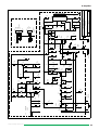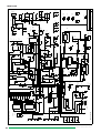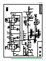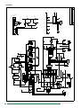
1
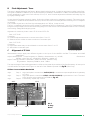
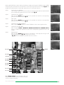
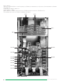
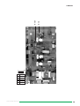
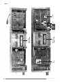
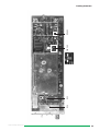
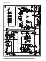
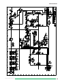
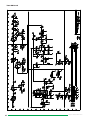
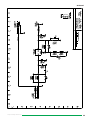
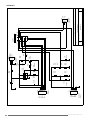
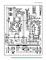
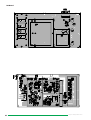
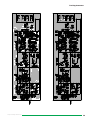
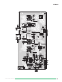
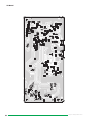
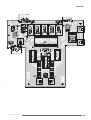
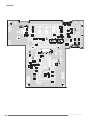
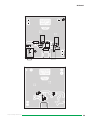
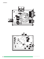
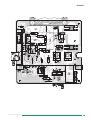
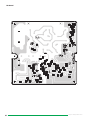
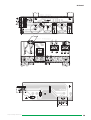
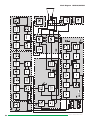
ENGLISH
®
Instruments
Spectrum
analyzer
HM5011
HM5010
4S-5010-0010
09 JUN 1998
SERVICE-MANUAL HM5011/5010
Service Manual
Adjustment Procedure
Circuit Diagrams
5
Alignment Procedure for HM5010/HM 5011 .........
A Control and Adjustment of
Supply Voltages ...............................................
B Final Alignment - Tuner .....................................
C Alignment - IF-Unit ...........................................
D Linearity of Frequency Display .........................
HM5010 XY-board ...........................................
Tuner ...............................................................
Tracking-Generator ..........................................
E Alignment of HM5011 Tracking Generator ......
5
6
6
7
10
11
12
13
Tracking-Generator .................................................
Tuner RA-Board ......................................................
Tuner RB-Board ......................................................
IF-Amplifier .............................................................
Main board .............................................................
X-Y Board ...............................................................
FC-Board ................................................................
PA-Board ................................................................
CRT-Board ..............................................................
Power supply Board ...............................................
RA-Board ................................................................
Tracking-Generator .................................................
RB-Board ................................................................
Main board .............................................................
Main board .............................................................
XY-Board .................................................................
XY-Board .................................................................
FC-Board ................................................................
FC-Board ................................................................
PA-Board ................................................................
CRT-Board ..............................................................
PS-Board ................................................................
PS-Board ................................................................
PS-Board ................................................................
Block Diagram HM5010/HM5011 ..........................
15
16
17
18
19
20
21
22
23
24
25
26
27
28
29
30
31
32
33
34
35
36
37
38
39
Subject to change without notice
HM5010/5011
2
SPECTRUM ANALYZER
Specifications
Frequency
Frequency range: 0.15MHz to 1050MHz (-3dB)
Center frequency display accuracy: ±100kHz
Marker accuracy: ±(0.1% span + 100kHz)
Frequency display res.: 100kHz (4½ digit LED)
Frequency scanwidth: 100kHz/div. to 100MHz/div.
in 1-2-5 steps and 0Hz/div. (Zero Scan)
Frequency scanwidth accuracy: ±10%
Frequency stability: better than 150kHz / hour
IF Bandwidth (-3dB): Resolution: 400kHz and
20kHz; Video-Filter on: 4kHz
Sweep rate: 43Hz
Amplitude
Amplitude range: -100dBm to +13dBm
Screen display range: 80dB (10dB / div.)
Reference level: -27dBm to +13dBm
(in 10dB steps)
Reference level accuracy: ±2dB
Average noise level: -99dBm (20kHz BW)
Distortion: <-75dBc; 2nd and 3rd harmonic
3rd order intermod.: -70dBc
(two signals >3MHz apart)
Sensitivity: <5dB above average noise level
Log scale fidelity: ±2dB (without attn.) Ref.: 250MHz
IF gain: 10dB adjustment range
Spectrum Analyzer HM5010 / HM5011
Input
Input impedance: 50Ω
Input connector: BNC
Input attenuator: 0 to 40 dB (4 x 10dB steps)
Input attenuator accuracy: ±1dB/10dB step
Max. input level: +10dBm, ±25VDC (0dB attenuation)
+20dBm (40dB attenuation)
Tracking Generator
Output level range: -50dBm to +1dBm
(in 10dB steps and var.)
Output attenuator: 0 to 40dB (4 x 10dB steps)
Output attenuator accuracy: ±1dB
Output impedance: 50Ω (BNC)
Frequency range: 0.15MHz to 1050MHz
Frequency response: ±1.5dB
Radio Frequency Interference (RFI): <20dBc
Divers
AM-Demodulator output for head-sets.
Permissible load impedance >8Ω
General
Display: CRT. 6 inch, 8 x 10 div. intern. graticule
Trace rotation: Adjustable on front panel
Line voltage: 115 / 230V ±10%, 50-60Hz
Power consumption: approx. 20W
Operating ambient temperature: 0°C..+40°C
Protective system: Safety Class I (IEC 1010-1)
Weight: approx. 7kg
Cabinet: W 285, H 125, D 380 mm
Subject to change without notice
5/96
Frequency Range 0.15MHz - 1050MHz.
4½ Digit Display (Center & Marker Frequency, 0.1MHz resolution)
–100 to +13dBm Amplitude Range, 20kHz, 400kHz and Video-Filter
Tracking-Generator (HM5011 only):
Frequency range: 0.15MHz - 1050MHz.
Ω).
Output Voltage: +1dBm to –50dBm (50Ω
Evolution of the original HM5005/HM5006 has led to the new HM5010/
HM5011 Spectrum Analyzer/Tracking Generator which now extends
operation over 1 GHz (frequency range 0.15 to 1050 MHz). Both fine and
coarse center frequency controls, combined with a scanwidth selector
provide simple frequency domain measurements from 100 kHz/div. to 100
MHz/Div.. Both models include a 4½digit numeric LED readout that can
selectively display either the center or marker frequency. The HM5011
includes a tracking generator.
The HM5010/5011 offer the same operation modes as the HM5005/5006.
The instruments are suitable for pre-compliance testing during development
prior to third party testing. A near-field sniffer probe set, HZ530, can be used
to locate cable and PC board emission "hot spots" and evaluate EMC problems
at the breadboard and prototype level. The combination of HM5010 / 5011 with
the HZ530 is an excellent solution for RF leakage/radiation detection, CATV/
MATV system troubleshooting, cellular telephone/pocket pager test and EMC
diagnostics. There is an optional measurement output for a PC which makes
documentation of results easy and affordable with the HO500 Interface.
Accessories supplied: Line Cord, Operators Manual. Optional accessories, 50Ω
Ω-feedthrough termination HZ22
Viewing Hood HZ47, Near Field Probe Set HZ530, Carrying Case HZ96-2, Transient Limiter HZ560
HO500 Computer Interface for HAMEG Spectrum Analyzer
This HO500 computer interface offers the facility to transfer a calibrated frequency
spectrum from any HAMEG spectrum analyzer to a PC. The HO500 interface is a
8 bit ISA BUS card installed in the PC, which transfers data via an interface cable.
The software supplied allows a hard copy print out (including parameters) of the
frequency spectrum, in Windows Format. Signal aquisition occurs 2 to 3 times per
second.
The picture consists of 10 bit vertical by approx 3600 point horizontal display. The PC
monitor display is in SVGA Format with 800 x 600 pixels. For comparison
measurements, a previosly stored reference curve can be recalled. The software
supplied works under Windows 3.1, 3.11 and WIN95. A simple XY analog output is
required to connect the HO500 to the spectrum analyzer.
3
Subject to change without notice
EMC-MEASUREMENT EQUIPMENT
Specifications
Frequency
Frequency range: 0.1MHz to 1000MHz
(lower frequency limit
depends on probe type)
Output impedance: 50 Ω
Output connector: BNC-jack
Input capacitance: 2pF
(high imped. probe)
Max. Input Level: +10dBm
(without destruction)
1dB-compression point: -2dBm
(frequency range dependent)
DC-input voltage: 20V max.
Supply Voltage:
6V DC
4 AA size batteries
Supply-power of HM5010/5011
Supply Current:
8mA (H-Field Probe)
15mA (E-FieldProbe)
24mA(High imp.Probe)
Probe Dimensions: 40x19x195mm (WxDxL)
Housing:
Plastic; (electrically
shielded internally)
Package contents: Carrying case
1 H-Field Probe
1 E-Field Probe
1 High Impedance Probe
1 BNC cable (1.5m)
1 Power Supply Cable
(Batteries or Ni-Cads are not included)
Near Field Sniffer Probes HZ 530
SCALE = 10dB/DIV.
The H-Field probe provides a voltage to
Frequency Response E-Field Probe (typical)
Subject to change without notice
The High-Impedance Probe
The high-impedance probe (Hi-Z) permits
the determination of the radio frequency
interference (RFI) on individual contacts or
printed circuit traces. It is a direct-contact
probe. The probe is of very high impedance
(near the insulation resistance of the printed
circuit material) and is loading the test point
with only 2 pF (80Ω at 1 GHz). Thereby one
can measure directly in a circuit without
significantly influencing the relationships in
the circuit with the probe.
One can, for example, measure the quantitative effectiveness of filters or other
blocking measures. Individual pins of ICs can
be identified as RFI sources. On printed
circuit boards, individual problem tracks can
be identified. With this Hi-Z probe individual
test points of a circuit can be connected to
the 50Ω impedance of a spectrum analyzer.
The E-Field Monopole Probe
The E-field monopole probe has the
highest sensitivity of the three probes. It is
sensitive enough to be used as an antenna
for radio or TV reception. With this probe the
entire radiation from a circuit or an equipment
can be measured. It is used, to determine the
effectiveness of shielding measures. With
this probe, the entire effectiveness of filters
can be measured by measuring the RFI which
is conducted along cables that leave the equipment and may influence the total radiation.
In addition, the E-field probe may be used
to perform relative measurements for certification tests. This makes it possible to apply
remedial suppresion measures so that any requalification results will be positive. In addition,
pre-testing for certification tests may be performed so that no surprises are encountered
during the certification tests.
SCALE = 10dB/DIV.
The H-Field Near-Field Probe
the connected measurement system which
is proportional to the magnetic radio
frequency (RF) field strength existing at the
probe location. With this probe, circuit RF
sources may be localized in close proximity
of each other. The H-field will decrease as
the cube of the distance from the source. A
doubling of the distance will reduce the Hfield by a factor of eight (H = 1/d³); where d
is the distance.
In the actual use of the H-field sensor one
observes therefore a rapid increase of the
probe’s output voltage as the interference
source is approached. While investigating a
circuit board, the sources are immediately
obvious. It is easily noticed which component
(i.e. IC) causes interference and which does
not. In addition, by use of a spectrum analyzer,
the maximum amplitude as a function of
frequency is easily identified. Therefore, one
can eliminate early in the development components which are not suitable for EMC
purposes. The effectiveness of countermeasures can be judged easily. One can investigate shields for "leaking" areas and cables
or wires for conducted interference.
SCALE = 10dB/DIV.
The HZ530 is the ideal toolkit for the
investigation of RF electromagnetic
fields. It is indispensable for EMI precompliance testing during product
development, prior to third party testing.
The set includes 3 hand-held probes
with a built-in pre-amplifier covering the
frequency range from 100kHz to over 1000
MHz.
The probes - one magnetic field probe,
one electric field probe, and one high
impedance probe - are all matched to the
50Ω inputs of spectrum analyzers or RFreceivers. The power can be supplied
either from batteries, Ni-Cads or through a
power cord directly connected to an
HM5010/HM5011 series spectrum
analyzer.
Signal feed is via a 1.5m BNC-cable.
When used in conjuction with a spectrum
analyzer or a measuring receiver, the
probes can be used to locate and qualify
EMI sources, as well as evaluate EMC
problems at the breadboard and
prototype level. They enable the user to
evaluate radiated fields and perform shield
effectiveness comparisons. Mechanical
screening performance and immunity tests
on cables and components are easily
performed.
Frequency Response H-Field Probe (typical)
Frequency Response High Impedance Probe
(typical)
4
Alignment Procedure for HM5010/HM 5011
Attention! The opening of covers or removal of parts is likely to expose live parts and accessible terminals
which can be dangerous to life. Maintenance, service and alignment should be carried out by qualified
personnel only, which is acquainted with the danger involved.
When aligning the HM5010/5011 it is assumed that all sub-assemblies of the instrument are completely pretested and
working correctly. The tuner, IF-unit, and tracking generator should be pre-aligned. When aligning a HM5010, a separate
tracking generator unit must be available and connected to the HM5010 for some specific adjustments.
Prior to the alignment procedure, the instrument must warm up for 60 minutes.
All adjustments are carried out by means of a plastic screw driver or a ceramic adjustment tool.
The alignment is divided into the following steps:
A Checking of supply voltages
D Linearity alignment
B Alignment of the tuner
E Tracking generator alignment
C Alignment of the IF-unit
F Check of overall adjustment
The numbering system is related to the respective pictures. Screen shots are designated as PIC
1 HF-Synthesizer 100 kHz to 1000 MHz, i.e. HM 8133
2 BNC cable, BNC T-connector, 2 x 10dB attenuator 50 Ohm
1 Voltmeter i.e. HM 8011-3
Control and Adjustment of Supply Voltages
adjust:
adjust:
adjust:
adjust:
12V to an accuracy of ±0.1V
via Trimpot 4 PIC 1
minimum brightness
via Trimpot 2 PIC 1
maximum brightness
via Trimpot 3 PIC 1
astigmatism
via Trimpot 1 PIC 1
check:
check:
check:
check:
check:
check:
– 12V
+12V
+5V
–5V
+38V
+138V
tolerance ± 0.2V
tolerance ± 0.1V
tolerance ± 0.2V
tolerance ± 0.2V
tolerance ± 1V
tolerance ± 1V
1
1
2
3
4
5
6
The corresponding voltage test points to check direct voltage can
be measured at the measuring connector strip (see PIC 2).
+138V
+38V
GND
+5V
+12V
-12V
Basic adjustment:
When Y-pos. knob is snapped in on front board, adjust beam
approx. 2 mm below bottom graticule line via R801.
4
PIC 1. PS-Board
5
Instrument Rear Side
1
A
PIC 2. XYF-Board (partial)
3
1
2
CRT-Board
Subject to change without notice
B
Final Adjustment - Tuner
The tuner is already aligned by the factory. When changing the 1st mixer, it might be necessary to realign cavity filter:
Set signal to 500MHz -27dBm to input, center frequency to 500MHz, Scanwidth to 0.5MHz, turn all three M3 screws
to max. amplitude. In case curve is not uniform, coils L1, L2, and L3 can be adjusted to maximum uniformity (fig. 22)
by slightly bending them.
In case signal in frequency range is shacky, 2nd local oscillator might not be snapped in correctly. The correct snapin of the PLL is visible via the lock detect LED (D2), which has to be lit constantly without flickering if PLL is snappedin correctly.
The oscillator signal has to be fixed (crystal dependent) at 1.32GHz, it may not drift.
The PLL is snapped-in when the tuning voltage VT (measure at PAD1) is between 0.5 and 4.5V. The alignment will
bring the tuning voltage to the center of the tuning range. VT of the 2nd LO has to be between 2V and 2.5V. Constantly
check tuning voltage while aligning tuner.
Alignment is necessary in two cases: VT<2.0V and VT>2.5V.
• Case 1 VT<2.0V
Correction:
a ) Solder all adjustment areas to connect trace from C1 to C2.
b ) Remove excess solder at center conductor of resonator pad.
• Case 2 VT>2.5V
Correction:
a ) Adjustment areas may not be soldered to connect trace from C1 to C2.
b ) Add solder to resonator pad.
C
Alignment of IF-Unit
fig. 22 for HM5010
Measurement setup: Apply two different signals to the input of the HM5011 via BNC T-connector and 10dB
attenuators.
Adjust HM5010/5011: Center frequency to 500MHz; all attenuators on (–40 dB)
Bandwidth
400kHz; video filter off; scanwidth 0.5MHz/div.; marker off.
Adjust Tracking Generator: Attenuator –20dB; level max. (HM5011 only)
RF-generator: frequency 500MHz; level –5dBm
The output voltage of the tracking generator is visible on the screen by an overlay of the fixed frequency. A "zero" point
fig. 23
is visible within the signal to the right or to the left of the 500MHz spectral line (fig.
23) (5011 only).
IF Filter Curve at 400kHz Bandwidth
align:
Step 1
Align (with plastic screw driver) Coil L1 (PIC 5) to maximum output amplitude and symmetry
to Y-axis.
Step 2 Align (with plastic screw driver) Coils 3 + 4 + 13 + 14 (PIC 5) to symmetrie to Y-axis. The "zero"
fig. 23).
point must be at the maximum (at 500MHz) (fig.
Stept 3 If necessary, repeat step 1 and 2.
align:
align:
VR 3
VR 1
L 10
L7
L 11
L8 L4
L 12
L9
L 13
L 14
L3
L1
fig. 23 for HM5011
VR 4
Subject to change without notice
VR 2
PIC 5
IF-Amp
Board
6
IF Filter Curve at 20kHz Bandwidth (HM5010)
align:
Step 1
Align (with plastic screw driver) Coils L7+8+9+10+11+12 until "zero" point is exactly centered
at 500MHz (as with 400kHz Bandwidth).
Watch for symmetry of Filter Curve.
IF Filter Curve at 20kHz Bandwidth (HM5011)
Pre-Alignment: Remove T-connector. Connect tracking generator module directly to the input of the HM5011. Turn
off attenuators on tracking generator module and on HM5011 (0 dB). The output voltage of the tracking generator
module is now visible as horizontal line (with slight ripple).
adjust:
Step 1
adjust:
Step 2
Adjust (with plastic screw driver) Coils 7 + 8 + 9 + 10 + 11 + 12 to maximum screen height
of displayed output voltage. Add attenuators of HM5010/5011 as soon as "line" has reached the
middle of the screen (–30 dB).
This alignment has to be performed repeatedly in order to optimize settings.
Fine Alignment: Connect BNC-T-connector again as in the beginning of the IF alignment. Set attenuator of tracking
generator module to –20dB, scanwidth to 0.5 MHz/div. If necessary, re-adjust center frequency
(adjust 500MHz spectral line to screen center). "Zero" point is now visible to the right or to the
fig. 24).
left of screen center (amplitude maximum) (fig.
adjust:
Step 1
adjust:
Step 2
Align (with plastic screw driver) Coils L7+8+9+10+11+12 until "zero"
point reaches maximum. Watch for symmetry of Filter Curve.
This alignment has to be performed repeatedly in order to optimize
settings.
fig. 24
IF Gain - Adjustment of different Bandwidths
Set scanwidth to 0.2MHz/div. Switch bandwidth repeatedly between 400kHz and 20kHz. The distance between the
output voltage (line) of the tracking generator and tge 400MHz amplitude may not vary. If the amplitude values do
not match exactly, adjust by means of R-trimmer VR2 (PIC5)
(PIC5).
Linearity of IF-Amplifier Gain
The linearity of the IF-amplifier gain has to be checked through the entire display range. Apply a 400MHz (-27dBm)
signal directly to the input of the HM5010/5011. Adjust scanwidth to 5MHz/div, release attenuator switched (0 dB),
select filter bandwidth of 400kHz. The spectral line should reach the upper screen edge. Use attenuators to reduce
signal in 10db steps, whereby each individual attenuation step has to reduce the level by 10dB ±1dB. In case deviation
is as follows:
- A the drop of the individual attenuation steps is larger than 10dB ± 1dB, or
- B the drop of the individual attenuation steps is smaller than 10dB ±1dB, the linearity of the attenuators has to be
adjusted as follows:
Set attenuator to -40dB. Adjust spectral line exactly to -40dB (center line) via VR1, VR3, VR4. Then set attenuators
back to 0dB und adjust spectral line by means of trimpots VR802A and VR801 (XY board) to zero point and base
line to bottom graticule line. This procedure has to be repeated until the settings at -40dB and 0dB are correct.
D
Linearity of Frequency Display
Settings for HM5010/5011:
Center frequency at 500MHz; all attenuator switches released; filter bandwidth
400kHz; video filter off; scanwidth to 100MHz/div.; marker off.
Measurement Setup: Apply signal of 500MHz –27dBm to input of HM 5010/5011.
Check:
Check:
7
Basic setting: The HM5010/5011 has to be adjusted that the noise level touches the bottom graticule
line. The spectral line of 500MHz -27dBm reaches the top graticule line and is situated in the center of
the screen. Adjust 500MHz spectral line exactly to screen center via X-pos knob (on front of the unit).
Upper frequency limit: Check if frequency of minimum 1050 can be set as center frequency.
Subject to change without notice
Adjust HM5010/5011 to basic setting (see above). Apply input signal of 100MHz, level +7dBm
fig. 7)
Overriding the input allows for the harmonics of the input signal to become visible (fig.
7). This
simplifies the adjustment of individual spectral lines in horizontal direction.
adjust:
Spectral line at 400MHz
Turn X-ampl. knob on front of instrument to have the 4 spectral lines matched with
fig. 8
the corresponding graticule lines on the screen(fig.
8).
adjust:
Spectral line at 100MHz
With Trimpot RV171 align to match this spectral line with the corresponding
fig. 9
graticule line on the screen (fig.
9).
adjust:
Zero Peak
With Trimpot RV173 align to match this spectral line with the corresponding
fig. 9
graticule line on the screen (fig.
9).
adjust:
Spectral line at 600-1000MHz
With Trimpot RV186 adjust to match 700MHz to the correct graticule line.
adjust:
Spectral line at 800 MHz;
With Trimpots RV181 + RV183 for 900MHz and RV197 for 1000MHz (PIC 3)
adjust to match this spectral line with the corresponding graticule line on the
screen.
fig. 7
fig. 8
fig. 9
adjust:
Beam length
With Trimpot RV101 adjust beam to end approx. 1mm beyond the right CRT
Fig. 11 - base line too short)
boundary (graticule) (Fig.
Fig. 10 - 300 to 1000MHz spectral lines not correct )
(Fig.
fig. 10
RV 112
RV113
fig. 11
RV 149
RV 101
RV 183
RV 181
RV 186
RV 197
RV 171
RV 173
PIC 3 - MB-Board
Set Trimpot RV113 that frequency will not
display below 990MHz when center frequency
is set to lowest frequency
Subject to change without notice
8
Adjust Marker.
Settings on HM5010/5011: Center frequency to 500MHz, all attenuators in off position, filter bandwidth to 400kHz,
video filter off.
Scanwidth to 100MHz, Marker on.
Signal 100MHz +7dBm.
Adjust Marker to 500MHz display and set to 500MHz mark on screen via RV149 (PIC 4).
Turn Marker left to max. and adjust to 990MHz via RV112.
VR 2
VR 3
L 10
L7
L 13
L 11
L8 L4
L 12
L9
L 14
VR 4
RV 112
L3
VR 1
L1
RV 113
RV 149
RV 183
RV 101
RV 181
RV 186
RV 197
RV 171
RV 173
PIC 3 - Main-Board
9
Subject to change without notice
RV 801
RV 802A
XY-Board
1
1
2
3
4
5
6
Subject to change without notice
+138V
+38V
GND
+5V
+12V
-12V
10
1st
Mixer
11
M3 Screws
Cavity - Filter
M3 Screws
Cavity - Filter
C1 C2
MPAD1
Tuner
Subject to change without notice
RV4
RV3
C68 C69
MPAD2
Tracking-Generator
Subject to change without notice
12
E
Alignment of HM5011 Tracking Generator
1.
Required Instruments:
1.1
1.2
1.3
1.4
1.5
Spectrum Analyzer - minimum 1000MHz
Completely assembled HM5011
Multimeter to measure DC voltage
Oscilloscope, i.e. HM303
Coax cabel
2.
Preparation:
2.1
2.2
2.3
2.4
2.5
Assemble Spectrum Analyzer completely (without case).
All sub-assemblies have to be pre-checked.
HM5011 has to be warmed up.
Connect VCO output of RA board to VCO input (MCX connector).
Connect 12MHz reference clock of TG board to RCA connector ST1 on RB board.
3.
Check Signalling Lines
Cable connection W1
Pin Nr.
1
2
3
4.
Signal
Supply OP
Supply
Supply PLL
Check Supply and Bias Voltages
Comp.Nr.
C1
C2
C11
C6
C9
C12
5.
Description
-12V
+12V
+5V
Pin Nr.
1
1
3
5
3
3
Description
1. VCO Amp.
2. VCO Amp.
fix LO Amp.
Var. Amp.
1. Power Amp.
2. Power Amp.
Voltage
+5.8 V
+5.8 V
+5.9 V
+5.6 V
+3.6 V
+4.8 V
Alignment of fixed LO
5.1 The 2nd LO oscillates at a frequency of 1.35 GHz. The level at the mixer input IC3 Pin2 is -17dBm. Oscillation
of the 2nd LO can also be measured with the H or E-Field Probe (HZ530).
5.2 Lock-Detect LED (D4) will confirm the correct PLL lock when lighting up without flickering or going out.
The oscillator signal has to remain fixed crystal dependent) at 1.35GHz and may not drift. PLL is locked if tuning
voltage VT (measure at PAD2) is between 0.5 and 4.5V. Align tuning voltage to medium tuning range. VT of
fixed LO should be between 2 and 2.5V. The tuning volage has to be check constantly during alignment.
Place coax resonator CR2 bottom side to the edge of soldermask next to center conductor, and solder on the
left and the right side.
5.3 Alignment is necessary in two cases: VT<2.0V and VT>2.5V.
• Case 1 VT<2.0V
Correction:
a ) Solder all adjustment areas to connect trace from C1 to C2.
b ) Remove excess solder at center conductor of resonator pad.
• Case 2 VT>2.5V
Correction:
a ) Adjustment areas may not be soldered to connect trace from C1 to C2.
b ) Add solder to resonator pad.
13
Subject to change without notice
6.
Control of fixed LO-Level
6.1
To check 2nd LO-level, cap C20 (22pF) has to be removed and 50Ohm Coax-cable has to be connected to 13dB attenuator of output. Connect other end of coax cable with adequate test analyzer.
Adjust test analyzer to 1.35 GHz center frequency; the LO-level to be measured has to be -17dBm (±1 dB)
(consider attenuation of cable).
If cap is not removed and coax cable is connected parallel to mixer to the VCO-branch, a level of approx. -24
dBm (±1dB) should be measured due to decreased load resistance.
6.2
6.3
7.
Check of VCO
7.1
7.2
7.3
Adjust HM5011 to Zero Scan, center frequency to 500MHz.
Remove Cap C14 (22pF), connect one side to attenuator output, other side stand up in the air.
Connect Cap side sticking up in the air to center conductor of 50 Ohm cable. Solder shielding of cable directly
next to Cap to ground. Connect other end of Cap to Analyzer input (i.e. Advantest R3361A). Start 1.35GHz Stop 2.35GHz reference level: 0dBm.
VCO signal which can be observed on the test analyzer has to shift according to center frequency (tuning
voltage). Tuning range has to be at least from 1350 to 2350 Mhz. continuously and without interruption. It
should not go under absolute level of +7dBm (coax cable of 1 mtr. has 1-2 dB of attenuation at 2GHz). Level
has to be between +7 dBm and +10 dBm.
Connect coax cable parallel to 1st mixer to VCO-branch. A level of +5 dBm to +8 dBm due to decreased load
resistance over frequency band.
7.4
7.5
8.
Check of Attenuators:
8.1
8.2
8.3
8.4
8.5
Set -30dB attenuation to Tuner and to 0dB attenuation to TG.
Set Center Frequency to 500MHz, 100MHz/Div. span.
Connect tracking generator to tuner input.
TG-line has to be visible.
Switch on additional attenuators. Attenuation for each attenuator switch has to be 10dB (±1 dB)
9.
TG Level Adjustment:
9.1
9.2
9.3
9.4
9.5
9.6
9.7
Connect TG to reference analyzer.
Set HM5011 to Zero Scan and 500MHz Center Frequency.
Release all attenuator buttons of TG (0-dBm) and turn TG-level to maximum.
Adjust amplitude to +1dBm with Pot RV4 on TG.
turn TG-level to minimum.
Adjust amplitude to -10dBm with Pot RV3 on TG.
Amplitude has to be adjustable now between +1dB and -10dB.
10.
Final Check
10.1 Position of TG-level has to align in both bandwidths (400kHz and 20kHz). If necessary, align with IF-Amp.
10.2 TG-level knob has to be adjustable from +1 to -10dBm.
Subject to change without notice
14
Tracking-Generator
15
Subject to change without notice
Tuner RA-Board
Subject to change without notice
16
Tuner RB-Board
17
Subject to change without notice
Subject to change without notice
IF
2
+12V
CD1
1nF
IF IN
IF AMP
C2
47p
C1
8p2
C17
0.1u
R19
4K75
T3
BC557
1
30.0 MHz
22p
C3
CD2
1nF
R40
2K21
R21
100k
1N4148
D2
D1
1N4148
500mVpp
BW
FROM TUNER
2nd IF OUT
C4
8p2
RF2
F19
R11
4K75
C15
22p
2.2k
R10
+12V
250mV
+8V(12.5 kHz)
0V(250 kHz)
C18
120p
C19
1p8
VR1
200R
TUNER GAIN
COMP.
F1
RF3
R1
100k
C10
10n
C9
0.1u
C16
0.1u
C20
270p
RF2
F9
T2
BF961
RF2
F3
R9
3K32
R8
221R
C21
270p
C23
120p
C22
1p8
VR2
50K
C13
220p
RF2
F4
C12
33p
C24
10n
C25
10n
F7
RF2
R7
10K0
R2
47R5
R18
470k
C14
220p
C11
82p
C5
39p
R17
47R5
C27
10n
R16
181R
R13
100k
221R
R15
XT1
27.125MHz
R3
2K21
L2
0.82u
R6
10K0
T4
BF961
11V=
0.7Vpp
RF2
F10
NTC
R14
220R
C29
1p8
82p
C6
C33
120p
C28
120p
33p
C7
4.7V=
C32
1p8
R22
4K75
RF2
F11
C34
10n
C30
270p
RF2
F12
R4
470R
T1
BC547
R5
220R
D3
D4
CD3
1nF
1N4148
IF GAIN
BC547
T5
C39
10n
C37
0.1u
C26
0.1u
L5
15u
FROM ATTEN. RF UNIT S.1
R20
47K5
R23
22K1
1N4148
C31
270p
C8
10n
IF GAIN
RANGE
VR4
100K
R27
150k
C36
330p
R29
47R5
C38
180p
R30
3K32
VID
BW
L1102
L1101
400mVpp
R28
470K
RF2
F13
R32
100R
IF GAIN
+12V
+5V
R24
100R
T6
BF961
>2Vpp
100u
100u
VIDEO SIGNAL
VID
CD4
1nF
R25
180R
R26
100K
+5V
+12V
IF PCB
Date:
B
Size
Title
C35
10n
RF2
F14
6
5
4
3
2
1
NTC
R39
2K21
200mVpp
VR3
500R
NTC
R34
2K2
+8.8V
R37
3K92
8
9
7
6
G
VCC
May 5, 1994
IF5005.SCH
IF AMP HM5005/6
Sheet
1
4
U
F
2
C44
22p
C41
22u
IC1
MC3356P
HAMEG INSTRUMENTS GERMANY
22K
R38
C42
10n
C43
0.1u
7.6V=
R36
332R
OVERALL
GAIN
R31
4K75
R35
2K21
Document Number
C40
180p
R33
180R
GND
IF GAIN
+12V
+5V
+12V
GND
+5V
GND
VIDEO SIGNAL
BW
TO AL (RF UNIT)
KA901 S.1
1
2
3
4
KA1102
TO XYF PCB
P803 S.3
6
5
4
3
2
1
KA1101
1
2
3
4
5
11
12
13
15
16
17
18
19
20
of
8
REV
IF-Amplifier
31
32
-6V2
1k0
3
C206
0.1u
C205
0.1u
C204
0.1u
C203
0.1u
C202
0.1u
0.1u
1k00
R169
C169
0.1u
+5V
RV112
1K0
R129
6k19
/10turns
10K
2
RV110
14k3
R128
3
RV113
R177
2k74
RV111
10K
/10turns
2
C201
2
1
3
1
2
1
3
1
1 2 3 4 5 6
1 2 3 4 5 6
DIGITAL SECTION
MK-MIN
MKR
+VREF
CF-MIN
CF
+VREF
MOLEX6
P107
G D C B A T
N
V
D
C
TO FC PCB
W304 S.5
ANALOG SECTION
R199
1k00
+5V
INH
2
P201
MOLEX6
R216
51R1
QA
QB
QC
QD
1
2
3
4
5
6
P108
+ V T G G P
2 T V N N S
0
C D D
V
1 2 3 4 5 6
IC201A
74HC390
CLR
CKA
CKB
C119
0.1u
3
5
6
7
T108
BC850C
TO FC PCB
W305 S.5
R112
10k0
6
11
10
9
13
14
15
12
1
5
2
4
6
11
10
9
13
14
15
12
1
5
2
4
X1
MPOS
MOFF
GND
UREF
CF FINE
A
B
C
X0
X1
X2
X3
X4
X5
X6
X7
INH
1
4
C199
0.1u
X
A
B
C
X0
X1
X2
X3
X4
X5
X6
X7
IC102
HEF4051
X
TO AL PCB
W1203 S.1
C216
10nF
C117
22u
/35V
C118
22u
/35V
R111
33k2
3
3
IC103
HEF4051
C253
27p
%2
R116
100k
C108
1nF
13
12
2
3
1k00
R152
1
1
4
14
15
12
C254
56p
R253
10k0
3
4
100R
100R
301R
499R
1k00
3k01
4k99
10k0
30k1
49k9
R252
51R1
2
1
8
9
J201
COAX
R255
51R1
*
2
3
R10c
6M8
10
R262
51R1
9
51R1
R257
T102
BC850C
T101
BC860C
R123
274k
RV101
100K
SW-AMPL
R142
15k0
IC106A
LM324
C116
0.1u
1
*
13
12
9
8
1
0
R143
10k0
8
11
10
CLR
IC202B
74HC390
14
15
12
IC204D
HEF4011
HEF4011
IC204C
CKA
CKB
x100V
IC206C
74HC02
C136
0.1uF
8
+28V
2
3
C143
470p
R194
*
R172
2k74
5K0
RV171
L-A1
R171
1k50
IC101C
TL074
R120
22k1
R118
4k75
R117
22k1
R10d
6M8
C107
9
10
R186
221k
R193
61k9
R185
*
R191
30k0
R184
0R
R192
20k0
+28V
1
L-B
RV186
10K
R222
51R1
IC205E
74HCU04
11
3n3
C138
R125
8k25
R126
10k0
1
1
4
3
D181
BAW56
R183
10k0
RV183
100K
L-C2
R187
3k32
R188
D109
BAS16
+VREF
R119
22k1
IC205D
74HCU04
2
-6V2
R141
9k09
RT101
2k2
RT102
*
R267
1k00
R221
51R1
%10
TO TG J402 S.6
8 MHz OUT
13
13
11
10
9
C255
1nF
IC205F
74HCU04
R254
2k21
12
QA
QB
QC
QD
R133
56k2
-6V2
+VREF
R140
562R
0R
R189
R182
4k75
L-C1
RV181
5K0
R181
0R
+VREF
R10b
8k25
R115
10k0
R10a
10k0
C105
22nF
R114
5k11
R113
6M8
IC201B
74HC390
CLR
CKA
CKB
IC101D
TL074
14
IC101A
TL074
1
0.1u
C115
R251
51R1
XT254
8MHz
IC205B
74HCU04
3
R211
51R1
R151
18k2
VREF
-6V2
+28V
R109
R108
R110
R101
R102
R103
R104
R107
R106
R105
IC204A
R224
51R1
QA
QB
QC
QD
13
11
10
9
HEF4011
1
2
*
1
%2
R148
10k0
6M8
R190
R154
22k1
1
2
1
R
S
T
1
1
(PS)
1
0
C
L
K
1
%8
3
3
R223
51R1
D225B
BAW56
D225A
5
%1k 6
5
4
UNC
R225
2k21
IC205C
74HCU04
IC204B
HEF4011
1 1 1 1
3 2 1 5 4 2 3 6 4 5 7 9
6
IC205A
74HCU04
2
R149
10k0
5
6
7
R127
150k
3
2
4
IC206D
74HC02
1
R265
4k75
9
10
6
5
C262
4n7
PE
BAS16
D263
13
12
1
2
3
5
9
10
11
6
R261
51R1
R161
51R1
R266
51R1
R122
68k1
R264
51R1
11
12
IC206A
74HC02
-6V2
R121
221R
22k1
R167
D103
BAS16
R157
8k25
-6V2
0.1u
C109
+5V
SAWTH
C265
0.1u
D265
BAS16
R258
51R1
74HC02
IC206B
6
5
13
R259
51R1
+VREF
R160
100R
R158
1M00
D110
BAS16
8
IC106C
LM324
7
IC106B
LM324
R137
1M5
R138
1M5
C110
10nF
(VT)
R179
*
IC104B
LM393/M
R198
56k2
D180
*
R180
*
RV180
*
R156
221k
R250
22k1
RV149
10K
MKR-Offs.
3
R159
1k50
C130
4n7
R170
*
Q Q Q Q Q
1 1 1 1 1 Q Q Q Q Q Q Q
4 3 2 1 0 9 8 7 6 5 4 1
IC203
HEF4020
%4 2
%10k
%2k
R233
51R1
1
LM393/M
R146
*
R155
47k5
14
IC106D
LM324
+VREF
R197
47k5
R196
10k0
RV197
2k5
D144
*
R144
*
12
13
D197
BAS16
R175
*
IC104A
C129
0.1u
8
4
0.1u
C120
L-D
RV176
*
R195
0R
R145
*
110...210ns
-12V
C121
220p
R153
*
3
2
R124
1k50
-5V
+5V
-6V2
R249
51R1
R150
47k5
R147
*
3
R176
D171
BAV70
R173
47k5
RV173
500K
L-A2
R174
*
R178
*
7
R135
R134
47k5
2
1
4
LE
4
14
15
IC202A
R263
100k
74HC390
CLR
CKA
CKB
5
6
D102
BAS16
X
Y
C L P U G G
L E E N N N
K
C D D
1
2
3
P111
C141
0.1u
TO FC PCB
W303 S.5
P202
MOLEX6
+5V
R256
51R1
3
5
6
7
-5V
+5V
1
2
3
Subject to change without notice
Date:
C
Size
Title
R212
51R1
0.1u
D128
BAV99
(+13V)
1
2
LM
317
0.1u
C133
3
-6V2
R164
221R
1
R139
39R
R166
*
1
C
K
3
E
2
MMS0204 / 0.25W / 5%
3
B
A
1
MB50101B.SCH
MB PCB HM5010/11
November 6, 1995
C135
0.1u
/35V
Sheet
6
5
4
3
2
1
P109
4
BC860
BC850
BAS16
BAW56
BAV70
2
1
LM
7805
0.1u
C137
0.1u
of
3
0.1u
C103
C134
*
-12V
(+12V)
GND
(-5V)
+5V
+32V
C123
22u
/35V
C101
R163
2k05
R165
*
TO PS
P1006 S.8
C122
22u
/35V
C124
22u
C127
0.1u
IC107
*
*
C125
C132
*
6
5
4
3
2
1
TOP VIEW
2
O
U
I
N
ADJ
3
2
O
U
I
N
ADJ
HAMEG INSTRUMENTS GERMANY
0.1u
C111
R162
100R
IC108
LM317
R131
39R
R130
39R
R100
0R
+VREF
+28V
*
C139
0.1u
Document Number
0.1u
C104
R132
39R
GND
BLANK
GND
C142
22u
/35V
C102
P110
C
L
k
%4
MK
GND
XF
+20V
60mA
1
2
3
PCB
3
R168
C126
1000u
/16V
1
2
1
G
OU N IN
D
IC128
LM79L05
3
C140
*
2
TO CRT
W701 S.7
+5V
C131
0.1u
TO XY PCB
W801 S.3
QA
QB
QC
QD
1
2
3
+5V
C128
1000u
/16V
-6V2
1 2 3 4 5 6
IC101B
TL074
C112
1nF
-6V2
X1
X0
Y1
Y0
Z1
Z0
Z
IC105
HEF4053
8k25
R136
301k
C
B
A
INH
+28V
REV
Main board
Subject to change without notice
A
K
nc
C805
0,1uF
R835
12K1
R834
12K1
R826
*
BAS16
Top View
SOT23
22p
C807
R836
10K0
T806
BC860C
R841
100R
100R
R825
B
C
R837
10K0
R833
100K
R804
2K21
E
-12V
BFS20
BC860
BC850
R838
2K74
1K50
R808
R831
10R
1
2
3
R802
1K0
T801
BC847B
1K50
R809
T812
BF422
R806
100R
R866
30K1
1W
+73V
3-Pol
1
2
3
W802
R832
22K1
T805
BC850C
T804
BC850C
R807
100R
T803
BFS20
2.0mA
R814
100R
TO CRT PCB
P701 S.7
YF1
NC
YF2
+12V
R840
*
10K0
R852
R853
10R
C801
0.1u
D801
BAS16
1
R811
1K50
R812
1K50
T811
BF422
R824
100R
3
SXA 0411 Met. Fi. 1% 1W
R-Chip 5% 1206
R-Chip 1% 1206
C808
22p
R839
1K50
C806
0.1u
R830
10R
RV802A
4K7
Y AMPL
+133V
+73V
R865
30K1
1W
R827
2K21
C824
0.1u/250V
XF
GND
MK
C896
0.1uF
C822
FROM RB PCB
KA??? S.?
1
2
3
4
5
6
P807
1
2
3
4
5
6
R863
100K
T810
BD850
C818
10n
FROM MB PCB
P111 S.4
3
2
1
P801
R803
2k74
-12V
YPOS
GND
nc
+5V
+12V
R851
6K81
3
2
1
R801
4K75
BFS20
T802
10u/25V
R813
100R
R810
100R
R
0R
R
0R
R
0R
1
2
1
2
3
4
5
6
1
2
3
4
5
6
P804
FROM TG UNIT
KA501 S.6
GND
GND
GND
+5V
+12V
-12V
-12V
1
2
3
4
5
6
1
2
3
4
5
6
R896
*
C821
*
C819
0.1u
-12V
R898
22k1
-12V
R864
10R
*
C815
C816
*
0.1u
C814
C820
*
C828
+12V
0.1u
C813
6
5
4
3
2
1
C817
0.1u
10u/25V
R897
20k0
VIDEO SIGNAL FROM IF-AMP
0R
R
R828
10R0
C897
*
+12VY
-12VA
C823
10u/25V
R822
2k74
RV801
10K
YP-sym
R823
100R
R829
10R
P802
*
FROM FC PCB
KA301 S.5
VF
BW
+12V
+5V
GND
-12V
R895
100k
0.1u
3
R816
1K82
R815
+140V
C803
C802
0.1uF
R805
100k
R805A
100R
0.1u
C804
Y AMP
R845
22K1
R850
10R0
6
5
4
3
2
1
3
1
C871
2n2
2
6
5
4
3
2
1
+140V
+32V
GND
+5V
+12V
-12V
FROM PS
P1008 S.8
P805
FROM IF AMP
KA1101 S.2
(P803A / 5005)
P803
+12V
6
GND
5
+5V
4
GND
3
VS
2
BW
1
+12V
R847
10R
R846
22K1
RV804
4K7 A
X POS
C826
47u/250V
+140V
C809
0.1u
R871
221k
100R
R859
C811
0.1u
0.1u
C810
C893
0.1uF
3
R872
182k
5
6
(221K)
R874
*
R842
4K75
1
1
0R
R892
221R
2
1
R875
RV872
4k7 A
VOLUME
R873
2M2
D874B
*
(BAV99)
D874A
2
R862
1K50
C891
0.1uF
IC891
LM317
A
IN
D OU
J
+32V
1K82
R819
T807
BC847B
IC875B
TL082
7
2
1
R843
100R
2
R891
4K75
3
1
2
3
D802
1
R856
1K82
R855
1K82
R858
100R
47K5
1W
R868
+73V
1
2
3
4
5
6
W801
6-Pol
BAS16
1
2
3
4
5
6
C892
0.1uF
C878
10u/25V
R876
0R
R881
10k0
C812
0.1u
X AMPL
RV803
4K7 A
+140V
+20V...+125V
R867
47K5
1W
10R
R817
T813
BF422
+73V
R818
1K82
C873
100p
R821
100R
+140V
R820
100R
T808
BFS20
10u/25V
C827
C825
0.1u/250V
X AMP
R
0R
i.r.
R880
332k
2
3
-12VA
4
8
+12VY
R861
3K01
R870
4K75
R889
1K00
C889
0.1uF
3
R879
1K00
6
5
4
3
2
1
R844
0R
R860
4K75
R848
22K1
T809
BFS20
FROM MB PCB
W??? S.?
MOLEX6
6
5
4
3
2
1
P808
AUDIO - AMPL.
R882
68k1
IC875A
TL082
1
R877
0R
C879
0.1uF
R857
100R
T814
BF422
1.5mA
R854
100R
TO CRT PCB
P702 S.7
GND
GND
NC
XF1
+140V
XF2
Date:
C
Size
Title
-12V
nc
GND
nc
+5V
+28V
R884
100R
R887
332R
R883
100R
R849
100R
1
1
+12V
R888
0R
R889
0R
3
2
1
November 6, 1995
XY50101B.SCH
XYF PCB HM5010
Sheet
3-Pol
3
2
1
P870
3
NF
GND
+12V
FROM PA PCB
W??? S.?
P810
2.5MB6
1
2
3
4
5
6
CHECK-PTS.
HAMEG INSTRUMENTS GERMANY
R886
51R1
T886
BC860
220uF/16V
C882
T885
BC850
R885
51R1
Document Number
3
2
2
3
+5V
+140V
+32V
GND
+5V
+12V
-12V
of
REV
XY Board
33
34
3
TO MB PCB
P202 S.4
C L P U
L E E N
K
C
G G
N N
D D
/65mm
2
R317
100K
3
R318
100K
D307
1
4
BANDWIDTH
12.5kHz
2
5
ALPS
3
1
2
D306
6
BAW56
3
SW301
T304
BC850
10K0
R309
D304
BAS16
+5V
4K75
R301
IC300
ICM7217N
BAV70
1
R323
82K5
LED301
RED
UNCAL
R314
33K2
T303
BC860
C302
0.1u
T305
BC850
R311
182R
W303
6pol
2
1
D305
BAV99
1 2 3 4 5 6
C301
220u
/16V
L302
100uH
+5V
2
250kHz
12.5kHz
R336
*
R316
221R
R315
221R
R310
221R
R302
10K0
12
9
8
19
24
14
10
7
6
5
4
1
BAV70
D301
3
15
14
13
1
1
2
5
T306
BC860
3
ALPS
SW302
VIDEOFILTER
OFF
4
5
6
12
3
2
4
7
10
1
5
6
9
11
D302
BAV70
R330
10K0
ZERO
0.1
0.2
0.5
10
20
50
100
20
23
27
25
28
22
26
21
18
17
16
15
2
CO
Q0
Q1
Q2
Q3
Q4
Q5
Q6
Q7
Q8
Q9
R304
10K0
RST
CLK
ENA
IC320
HEF4017
1
2
3
OFF
ON
R329
*
R319
33K2
LED315
LED314
LED313
LED312
LED311
LED310
LED309
LED308
LED307
LED306
LED305
D303
BAS16
1
VF
BW
+12V
+5V
+5V
1
2
3
4
5
6
7
9
10
11
IC301
HP3603
1000MHz
1
1
3
C
L
P
R
1
0
1
C
L
Q
Q
Q
Q
R335
4k75
0
1
2
3
4
5
6
7
8
9
74HC42
IC308
C339
*
4
P
R
10
9
8
5
4
2
3
7
CLK
D
CLK
D
R340
475R
+5V
6
11
12
+5V
IC321B
74HC74
3
2
IC321A
74HC74
+5V
A
B
C
D
8
9
R338
*
R339
*
15
14
13
12
6
2
1
3
1
10
9
8
5
4
2
3
7
2K21
R342
TO MB PCB
P107 S.4
B A B C D T
W
V
Z
C
1 2 3 4 5 6
IC302
HP3603
100MHz
R341
475R
BAW56
D340
6
5
2
3
6pol
6
A
B
C
D
10
9
8
5
4
2
3
7
CI
CLK
PE
B/D
U/D
R331
33K2
+5V
IC306C
MC14011
10
CO
QA
QB
QC
QD
T331
BC850
1
IC307
+5V
1
1
MC14029
/70mm
R332
1K00
W304
9
8
7
6
11
14
2
D341
BAV70
IC303
HP3603
10MHz
3
221K
R344
2
1
R343
10K0
3
2
5
15
1
9
10
4
12
13
3
C308
0.1u
T340
BC850
4
5
6
1
SW304
R321
33K2
UP
10
9
8
5
4
2
3
7
1
2
3
2
3
+5V
R312
1M00
R322
1K00
+5V
C305
0.1u
R336
39R2
6
4
5
6
IC305
HP3603
0.1MHz
SCANWIDTH
IC306A
MC14011
1
R335
39R2
IC304
HP3603
1MHz
6
11
SW303
R320
33K2
1
2
3
MC14011
IC306D
5
6
IC306B
MC14011
R313
22K1
10
9
8
5
4
2
3
7
DOWN
12
13
4
1
C307
0.1u
C306
22n
1
BW
VF
C310
0.1u
MARKER
OFF
2
ALPS
4
3
5
6
SW305
TO XYF PCB
P802 S.3
C311
0.1u
3K32
R308
T302
BC860
T301
BC850
RV310
10K A
2
Subject to change without notice
Date:
C
Size
/300mm
R327
100R
R324
100R
C303
220u
/16V
MKR
LED303
GREEN
R303
150R
CTR
LED304
GREEN
TR
5K0
RV301
TO MB PCB
P108 S.4
X1
MPOS
MOFF
GND
UREF
CF FINE
/60mm
November 22, 1995
FC50101A.sch
FC-PCB HM 5010/11
P301
+5V
1
5
P302
TRACE
ROTATION COIL
1
Sheet
HAMEG INSTRUMENTS, GERMANY
W301
6pol
R326
100R
R325
100R
C304
0.1u
+5V
CF FINE
Document Number
- G + + B V
1 N 5 1 WF
2 D V 2
V
V
1 2 3 4 5 6
Title
L301
100uH
C309
0.1u
R307
10K0
R306
10K0
R359
100R
3
1
1
2
3
4
5
6
W305
6pol
of
REV
FC-Board
PA-Board
Subject to change without notice
22
23
1
2
3
4
5
6
KA702
6
5
4
3
2
1
P702
TO PS
P1002 S.8
TO XYF PCB
KA801 S.3
XF2
150V
XF1
NC
GND
GND
BLV
FCD
G1
-1925V
H1
H14
6
5
4
3
2
1
1
2
3
4
5
6
0.1u/100
C703
C701
0.1u
LL4151
D701
4
2
R704
1k0
5
1
R707
51k1
R708
47k5
IC701
6 CNY17
R701
681R
R702
68k1
20k0
VR701
R703
47k5
D703
TLSG5101
10K0
R705
D702
LL4151
1
2
3
51R1
0.1u/250
C702
T701
BC850
R710
GND
BLANC
GND
R706
10K0
TO MB PCB
P110 S.4
1
2
3
KA701
Date:
A
Size
Title
3
2
4
12
13
9
1
1 4
1
2
3
March 14, 1994
CRT5005.SCH
CRT PCB HM5005/6
1
2
3
P701
Sheet
7
TO XYF PCB
KA802 S.3
HAMEG INSTRUMENTS GERMANY
11
7
6
Document Number
D14-364
YF1
NC
YF2
of
8
REV
CRT-Board
Subject to change without notice
Power Supply Board
Subject to change without notice
24
RA-Board
25
Subject to change without notice
Tracking-Generator
Subject to change without notice
26
TO
RB-Board
27
Subject to change without notice
Main Board
Subject to change without notice
28
Main board
29
Subject to change without notice
XY-Board
Subject to change without notice
30
XY-Board
31
Subject to change without notice
FC-Board
Subject to change without notice
32
FC-Board
33
Subject to change without notice
PA-Board
Subject to change without notice
34
CRT-Board
35
Subject to change without notice
PS-Board
Subject to change without notice
36
PS-Board
37
Subject to change without notice
PS-Board
Subject to change without notice
38
Block Diagram HM5010/HM5011
39
Subject to change without notice
Oscilloscopes
Multimeters
Counters
Frequency Synthesizers
Generators
R- and LC-Meters
Spectrum Analyzers
Power Supplies
Curve Tracers
4S-5010-0010
Time Standards
HAMEG GmbH
Industriestraße 6
D-63533 Mainhausen
Telefon: +49 (0) 6182 / 800-0
Telefax: +49 (0) 6182 / 800-100
E-mail: [email protected]
[email protected]
Internet:
www.hameg.de
Printed in Germany