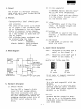
1
MZ-1E24
SHARP
SERVICE MANUAL
OOZMZIE24///E
RS-232C I NTER FACE
(FOR MZ80B, 700, 800)
MODEL
MZ-1E24
r---------------------CONTENTS----------------------~
1_ General··········································· 1
2. Features·········································· 1
3. Block diagram····································· 1
4. Hardware description··························· ... 1
5. Jumper block description··························l
6. Port address assignment························ ... 2
7. Port rate setup for each channel··········· ·······2
8. Connector signal mode·························· .. · 3
9. Troubleshooting······························ ..... 4
10. Use of the diagnostic program····················· 5
11. Circuit diagram·································· 6
12. Parts l i s t · · · · · · · · · · · · · · · · · · · · · · · · · · · · · · · · · · · · · · · 8
SHARP CORPORATION
-
M Z·1E24
2) Bit rate generator
1. General
The MOTOROLA MC144l CMOS Bit Generator is used with the external
1.S432MHz crystal oscillator. As
ten kinds of baud rates are obtain-
The MZ-lE24 is an RS-232C interface
card which can be used for the MZ-700,
MZ-SOO, and MZ-SOB.
ed on the output, the user can se-
2. Features
lect the desired rate.
·Incorporation of dual channels per-
3) Driver
mits independent data transmission
and recept ion.
The SN75lSS is used for the line
driver. The supply voltages are:
VCC+=12V, VCC-=-12V.
·Ten modes of baud rates can be chosen
by the jumper on the card which can
be set independently for each channel
·States of connector output signals
4) Receiver
to the external device can be assign-
The SN75lS9A lS used for the line
receiver. It operated under single
supply of 5V.
ed to the terminal or modern mode using the jumper.
·The following jumper assignment can
be attained using the jumper.
BI mode (MODE 1): MZ-SBI03
compatible.
ST mode (MODE 2): Sharp standard
RS-232C mode.
5) Z-SO SIO/O
The ZSO SIO/O is used for the
serial I/O drive.
5. Jumper block description
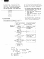
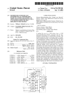
3. Block diagram
ADDRESS
pECO-
DER
JB-AI:
Selection of BI mode* and ST
mode* for the channel A.
JD-El :
Selection of BI mode* and
IDode* for the channel B.
All jumpers in the
-
CE
DRJVER
I
Z-80
sra/o
WI THCRYSTAL
.
Vcc+=+ 12V
Vcc-=- 12V
I
BI ST
BI mode
REdmI-
VER I--
RATOf
TTLLEVEL
jumper block
must be set to the same mode.
DRI VER'S
SUPPLY VOLTAGE
A ChtLnnel
B Channel
BIT RATE
GENE-
same
sr
±12VL EVEL
BI ST
mode
sr
Do not make all jumpers connected
in otherwise connection.
*BI mode
It is the mode compatible with the
MZ-SBlD3.
It has to be set in this mode when
operated under the system software
(i.e. DISK BASIC) which supports the
MZ-SBI03 to the MZ-SOB.
4. Hardware description
1) Address decoder
From the CPU is issued an S-bit
output for port assign address.
Since four successive ports are
used with
four port
assigning
the S-bit
switch.
the MZ-lE24, a successive
addresses are chosen by
the high· order 6 bits of
output using the dip
- 1 -
*ST mode
Standard RS-232C compatible mode.
It has to be set in this mode when
the MZ-800 or the MZ-700 (operated
under DISK BASIC).
--1_--MZ-1 E24
JB-A2:
JB-B2:
For
JB-A3:
JB-B3:
Selection of the baud rate for
the channel A.
Selection of the baud rate for
the channel B.
detail, refer to Section 7.
Sel"ction~0f the terminal and
modem mode for the channel A.
Selection of the terminal and
Logic level
1 0 1 1 o 0 x x
'---v----" '"----v-----'
0,1,2,3
B
fiX"
o or
represent either
1.
------~~~--~mo~d~e~m~mo~d~e~f~o~r:;t"h~e~c~h;a;n;n~e~I~B~.~------~In~e~~aaa~b±t-kr-is-tt~f&F-&~l~~c~-----JB-M :
tion of the Z-80 sro channel. The
address bit AO is used for selection
of the Z-80 sro command or data.
Setting up the RS signal
The RS (Request To Send) signal is set
to high by installing a jumper chip on
the ON side of jumper block JB-M.
ON OFF
10 I • • I
.
Sett1ng
up
•
s1gnal for
1088 i I-Setting up
(Factory setting) signal for
5
~
the RS
channel B
the RS
channel A
Jumper chips should normally be installed in the OFF position.
0
0
Data, channel A
0
1
Command, channel A
1
0
Data, channel B
1
1
Command, channel B
Choice
For the MZ-80B, 700 and 800:
The Z-80 CPU issues an 8-bit output
for the port address.
Since four successive ports are used
with the MZ-lE24, a successive four
port addresses must be selected by
assigning the high order 6 bits of the
8-bit address output using the dip
switch.
1
2
3
4
S
6
A2
A3
A4
AS
A6
A7
ON
ON
OFF
OFF
ON
OFF
Switch position
~
'The baud rate must coincide with
the specification of the software
used.
6. Port address assignment
Dip switch
number
Address
bit
Factory
setup
Al
7_ Port rate setup for each channel
As two channels, A and B, are provided
for this card, it is possible to set
baud rate independently for each channel.
The desired baud rate must be chosen
out of ten baud rates by making shortpin connection on JB-A2 and JB-B2.
The JB-A2 is used for the baud rate
assignment of the channel A and the
JB-B2 for the channel B.
Short pin 1
4
8
2
3
9
5
6
7
10
location
Baud rate 75 110 150 300 600 1200 1800 2400 4800 9600
Logic level
'"".-
ON
0
OFF
1
BO-B3H
."
.. '-"'-"
Notes:
Never try to insert more than two
short-pins at the same time as it
may possibly invite a destruction
in the rc.
Proper communication would not be
enabled, unless the baud rate is
identical at both sides.
The port addresses, therefore, have
been set to BOH, BlH, B2H, and B3H at
the factory.
- 2 -
-MZ-1E24
8. Connector signal mode
There are two 9-pin connectors used in
this card.
Channel A connector
(1)
\
®
®
®
®
) (!)
Gl
®
Gl
®
Channel B connector
®
®
(!)\
®
®
®
@
Gl
®
Gl
®
) (!)
Fig.4-2. Connector pln configuration
Signal assignment on connector pins
can be altered by changing jumper block
connections, by which the channel can
be assigned to either terminal or modem
mode.
RS-232C compatible signals are obtained
in the terminal and modem mode. That
is, binary signals are transferred in
the voltage level.
·Signal description
Pin No. Terminal mode
~l
Channel
A
4
5
Terminal mode
Yes
Yes
6
Modem mode
Yes
Yes
7
Table 4-4 Pin description
2
3
4
5
6
7
8
9
Transmit
data
Receive
data
Request
to send
Clear to
send
Equipment
ready
Data set
ready
Signal
ground
N.C
mode
FG
SD
RIi
RS
CS
to send
Data set
ready
Equipment
DR
ready
Signal
SG
ground
ER
readv
Signal
ground
Ready to
receive
9
RD Transmit
data
FG
RD
SD
RS N.C
CS Ready to
receive
ER Device
ready
Equipment
DR
ready_
SG Signal
ground
Clear
to
RR
send
RR
DR
ER
SG
CS
The following alteration takes place
when set to the modem mode.
Modem mode
Sefety
ground
Receive
data
Transmit
data
Clear to
send
Request
Device
8
Table 4-4 shows connector pln assignments in each mode.
For the pin number, refer to Table 4-2.
Connector
Terminal
pin No.
Safety
1
ground
data
Receive
data
Request
to send
Clear to
send
Equipment
ready
3
ChannelB
Safety
ground
SD Receive
data
FG
Transmit
2
Table 4-3 Channel mode
Mode
Safety
ground
1
Modem mode
FG
{
RD
BI mode
ST mode
2==-a
2==a
4
I
6.
•
5
• 7
{
5..
• 9
6 •
7
SD
·It has to be set in the terminal
mode when uSlng the acoustic coupler.
CS
RS
·Normally, it is operated in the
modem mode when the MZ-lE24 is connected with the RS-232C interface
incorporating printer and plotter.
However, thorough reading of the
instruction manual is required in
order to make proper use as there
may an exemption.
DR
ER
SG
N. C
- 3 -
--~-~--.
MZ-1E24
As the diagnostic program consists of
the board test and communication test,
the diagnostic program must be operated
depending on the trouble phenomenon.
oTo make direct connection with the
computer without intervention of
the modem, the following cable connection is required by operating the
one of sides in the terminal mode
·If the board test has not been completed successfully, there may the
following possible cause:
and the other side in the modem mode.
1
1
Z
2
3
3
4
5
4
5
6
7
8
9
6
7
8
9
1. Check for proper supply of the
clock (BUSO).
2. Check for a failure in the dip
switch.
3. Failure in the L804 or LS266.
4. Failure in the 810.
·If the communication test has not
been completed successfully, make
test in the following sequence.
9_ Troubleshooting
The diagnostic program must be used for
troubleshooting (see Paragraph 10).
Check the bit rate
generator.
out
Check the crystal
oscillator.
Program in
operation.
ChecK
if SD is
on.
es
Check if
±12V is on
across C.
if
RD is on
across D.
no
Check fora data
bus and SIO
failure.
no
Check the 75188
DC/DC converter.
no
Check the cable
and jumper.
no
TTL level
seen:::·>----l
Check the 75l89A.
.FailtJre in
the SIO
Address
decoder
Data
bus
A
SIO
r- j
SD
r---~
Cable
RD
X'
tal
Bit rate
genera tor
- 4 -
MZ'1E24
Then, the port No.
outputted.
10. Use of the diagnostic ptogram
B3, F7 is
1. Make the monitor connected with
8. Next, push the space bar. The
following message will appear if
entered correctly.
the MZ-800.
~
IMZ
A TO
~L.--,,8-,,-00,,-,
2.
B
OK
B
TO
A
OK
It will be in a failure if only
either side is on display with the
control waiting for a command entry.
Insert the diagnostic cassette
tape in the MZ-800 and load the
diagnostic program.
9. The test has been successful up to
Step 8, push the space bar to return
to the port test. After changing to
the ST mode, repeat the communication
test. Also, test the channel A in
the M mode and the channel B in the
T mode.
3. Set the MZ-lE24 to be tested in
the following manner:
1) Dip switch /jos.l, 3, 5 ... ON
2, 4, 6 •.. OFF
2) Set the JB-A3 to the T side,
'Baud rate test
th the JB-B3 to the M side, and
the JB-Al, BI to the BI mode.
Apply the universal canter probe
to the JB-A2, B2.
Check if the following frequency
is observed.
3) Set both switch of the JB-M
to the OFF side.
4) Set the JB-A2, B2 to the 1200
mode.
9600
4800
2400
1800
1200
600
300
150
4. Mount the MZ-lE24 to the slot of
the MZ-800, and connect the test
cable.
5. Enter A8H, which has been already
set, for the port address as
prompted on the monitor screen.
153.6K
76.8K
38.4K
28.8K
19.2K
9600
4800
2400
1760
1200
110
75
6. Push the space bar to get the
port address on display. The
following message will appear if
entered correctly.
(Only three
digits are
effective.)
'Signal level test
During the communication test, apply
the probe to the SD signal jumper
block of the JB-A3 and check if ±12V
is observed •
PORT NO = AB
7. Turn the dip switches, 2, 4, and 6,
to the ON side; and 1, 3, 5 to the
OFF side (=54H). Push the@key.
The following message will appear
if entered correctly.
• JB-M tests
Apply the probe to the RS signal
jumper block of the JB-A3. Check if
RS is stable at +12V when the JB-M
is ON.
PORT NO = 57
Parts code
Description
Diagnostic cassette
To perform the communication test,
UKOG-l038ACZZ
set the dip switches, 5, 2, and 1,
to the ON side; and 6, 4, 3 to the
OFF side (=80H). Push the CR key.
UKOGGI035ACZZ Test cable
- 5 -
tape
Price
rank
BB
BK
i
It
I
~
:a
...
.~
~
,~
U
•
~
A2A3
A4
AS
,,_
.,
471J
I
_._").
''''''''6
,-o+5V
_ I
: X6
=.::."J
"__
~+'"
'"
-12 v
"tj:"47 U
"
~"5V
-
J>--
l-/
--JDO-t
rj---JLH ..
I
•
~
,J[>----l
1Pb:::>-+
I
+5V~OC-Df
•
CON
GND
LSD4
0
Tl(DB~
RXOS 28
SI
3 "
00
"","
3 D2
3 .5
"
07
7 rEO
=1
1!XTWl~
TXO,QI
8
Jrr$Ii. 17
Ell
/'
,
: 91 ST '
I
ION
~
'J·-6~Ff
J8-83
I
~ __ I
91
ST
-.1
~
~----Ol-
JB-B1
:
,-
~~__"-~~-+-+~r,o
~HP----------~~
75"'"
12V
tm---d5+
+5V
oo1.7K
751B!!A
1-
, i1lf'?!t'iffOP
19-2--JJB-B1
~+12V
"
A
SLOT
.5
02
,;
"
"'~T'
____________.J~
I
I
I
I
I
s~
RR"
R 3
~
:~~i--------------!;Jj
J_~~!\3,
,
~,
OO
57
'
~
~
Ra
9PIN C()lNECTER
BI
JlFA1'
I
U:- '
~'
, _ 0:-
j~! i 11111 ~:~
-----'
05
~
7;
OR
~
"07
9TRR
Jro
""
•
lIT
fU111l
ffI!£1l
IEI
IEO
RESET
")
21 (NI'II)
GNO
20
19: 'ElTfIT
f7;
,.
,.,.
GNO
14 (HALT)
10
11:
04
SIDE
E
+5
03
"
4,
5'
5'
.'
7
(A15 )
(A 14)
(,01.13 )
(1.12 )
(,01.11)
"13
01
00
ONO
,"
________~-!£-9
,
~!
~: IF " b:j,<.------~:i
-12V
__ , sS===~~
::~~=f-o
'2 ' ~
O=Q.<'i=====J-ll!~
1 D1
00
01
D2
'03
38 D4
03"
"01
04
05
mm
RT
TIlT
"""""
20 BUSIII
1trr
H1
BUSSI
rn.-r
'"
34 B/A
R""'ESTI
S
-;-00 -o!-'-t~f2'51~.'~4---t~)r
,
'
r
0Tll'\~
6 lE
~"'5V
-"12V
: 81 57:
:: :112"='='
71T TTT TTT
19
1rmI~
9 VCC
i:I:
31 (;ND
i
rm~-'
~
III
+5V
:0 0 "'-;c;;-;c;----------'
I ' 1 ,
'S,-S;:" J B-A1
Gt.J 12
A"
vcc.~";--_.J
REn ~-2
,
~
"I
+"
2
33,~ ~
Al
RESH
1E0
IEI
tOM
M C14 4 11
24PIH
(AID)
(A 9 )
CA B )
A7
AS
A5
A3
..
A2
Al
AO
GNO
'"
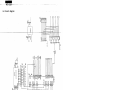
MZ-1E24
Pattern d"
"'.'" m
-
_-1.
Jumper
wire
- 7 -
..
------MZ-1E24
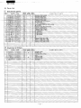
12. Parts list
rn Electronic parts
PARTS CODE
NO.
DESCRIPTION
lort ocket)
ine)
N:s
3
:z
lip swi
-TA
A
z
i
~line)
NV
~7 uF1
iP)
:N
' 6.5<hXlOl
AA
.
V
/-
i
i
V
v
V
~
,I
I
/6//-
i
i
))-
NV . )uF:
I
_A/=
±5%)
i
D
I
))-
I
a
i :0"
: ±5%'
W IOMO ±5%'
[2J Packing & Others
DESCRIPTION
.H
2
(20Qlfun)
_abe
In.,
N
C
8
1-:
. PWB
book
;Crew I X IOK)
ut (31
- 8 -
SHARP
SHARP CORPORATION
Industrial Instruments Group
Quality &. Reliability Control Center
492 Minoshocho, Yamatokoriyama,
Nara 639-11, Japan
Feb. 1985 Printed in Japan