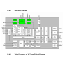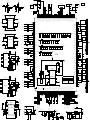
1
TABLE OF CONTENTS 1 INTRODUCTION................................................................................................................... 5 2 TUNER.................................................................................................................................... 5 2.1 General description of DTT71307: ................................................................................. 5 2.2 Features of DTT71307: ................................................................................................... 5 2.3 Pinning: ........................................................................................................................... 6 3 AUDIO AMPLIFIER STAGE WITH TDA8932 ................................................................... 6 3.1 General Description......................................................................................................... 6 3.2 Features ........................................................................................................................... 6 3.3 Applications .................................................................................................................... 7 3.4 Pinning ............................................................................................................................ 7 4 POWER STAGE ..................................................................................................................... 7 5 MICROCONTROLLER (VCTP) ........................................................................................... 8 5.1 General Features.............................................................................................................. 8 5.1.1 Controller: ............................................................................................................... 8 5.1.2 Audio:...................................................................................................................... 8 5.1.3 Video: ...................................................................................................................... 8 5.2 Multistandard Sound Processor (MSP) Features ............................................................ 9 5.3 Video Features............................................................................................................... 10 5.4 Controller Features........................................................................................................ 10 5.5 OSD & Teletext Features .............................................................................................. 11 5.6 Port Allocation .............................................................................................................. 11 6 DRX 3961A........................................................................................................................... 20 6.1 General Desription ........................................................................................................ 20 6.2 Features ......................................................................................................................... 20 7 SERIAL 64K I2C EEPROM M24C64WBN6 ...................................................................... 21 7.1 General Description....................................................................................................... 21 7.2 Features ......................................................................................................................... 21 7.3 Absolute Maximum Ratings.......................................................................................... 22 7.4 Pinning .......................................................................................................................... 22 8 CLASS AB STEREO HEADPHONE DRIVER TDA7050 ................................................. 22 8.1 General Description....................................................................................................... 22 8.2 Features ......................................................................................................................... 22 8.3 Pinning .......................................................................................................................... 23 9 SAW FILTER X6966M ........................................................................................................ 23 9.1 Features: ........................................................................................................................ 23 9.2 Pin configuration:.......................................................................................................... 23 9.3 Frequency response:...................................................................................................... 23 10 MPEG DECODER µPD61115 ......................................................................................... 24 10.1 DESCRIPTION............................................................................................................. 24 10.2 FEATURES................................................................................................................... 25 11 DRX 3973D....................................................................................................................... 25 11.1 Introduction ................................................................................................................... 25 11.2 Features ......................................................................................................................... 25 11.3 Applications .................................................................................................................. 26 12 PI6CX100-27MHz 3.3V VCXO for Set-Top Box Applications ...................................... 26 12.1 Features ......................................................................................................................... 26 12.2 Description .................................................................................................................... 26 13 74V1G08 ........................................................................................................................... 27 14 FMS6145........................................................................................................................... 27 15 IC DESCRIPTIONS AND INTERNAL BLOCK DIAGRAM ........................................ 28 15.1 LM1117......................................................................................................................... 28 15.1.1 General Description............................................................................................... 28 15.1.2 Features ................................................................................................................. 29 15.1.3 Applications .......................................................................................................... 29 15.1.4 Absolute Maximum Ratings.................................................................................. 29 15.1.5 Pinning .................................................................................................................. 29 15.2 LM1086......................................................................................................................... 29 15.2.1 General Description............................................................................................... 29 15.2.2 Features ................................................................................................................. 30 15.2.3 Applications .......................................................................................................... 30 15.2.4 Absolute Maximum Ratings.................................................................................. 30 15.2.5 Pinning .................................................................................................................. 30 15.3 MP1593 ......................................................................................................................... 31 15.3.1 General Description............................................................................................... 31 15.3.2 Features ................................................................................................................. 31 15.3.3 Applications .......................................................................................................... 31 15.3.4 Absolute Maximum Ratings.................................................................................. 32 15.3.5 Electrical Characteristics....................................................................................... 32 15.3.6 Pinning .................................................................................................................. 32 15.4 FDC642P....................................................................................................................... 33 15.4.1 General Description............................................................................................... 33 15.4.2 Features ................................................................................................................. 33 15.4.3 Absolute Maximum Ratings.................................................................................. 33 15.4.4 Pinning .................................................................................................................. 34 15.5 ANX9021 ...................................................................................................................... 34 15.5.1 Features ................................................................................................................. 34 15.6 24LC02.......................................................................................................................... 35 15.6.1 General Description............................................................................................... 35 15.6.2 Features ................................................................................................................. 35 15.6.3 10.6.3 Pinning ....................................................................................................... 36 15.7 µPA672T ....................................................................................................................... 36 15.7.1 General Description............................................................................................... 36 15.7.2 Features ................................................................................................................. 36 15.7.3 Absolute Maximum Ratings.................................................................................. 36 15.7.4 Pinning .................................................................................................................. 37 15.8 M74HC4052.................................................................................................................. 37 15.8.1 General Description............................................................................................... 37 15.8.2 Features ................................................................................................................. 37 15.8.3 Absolute Maximum Ratings.................................................................................. 37 15.8.4 Pinning .................................................................................................................. 38 15.9 Max809.......................................................................................................................... 38 15.9.1 General Description............................................................................................... 38 15.9.2 Features ................................................................................................................. 39 15.9.3 Absolute Maximum Ratings.................................................................................. 39 15.9.4 Pinning .................................................................................................................. 40 15.10 24LC21...................................................................................................................... 40 15.10.1 General Description........................................................................................... 40 15.10.2 Features ............................................................................................................. 40 15.10.3 Absolute Maximum Ratings.............................................................................. 40 15.10.4 Pinning .............................................................................................................. 41 16 SERVICE MENU SETTINGS.......................................................................................... 41 16.1 Video Setup ................................................................................................................... 41 16.2 AudioSetup.................................................................................................................... 42 16.3 Options 1 ....................................................................................................................... 42 16.4 Options 2 ....................................................................................................................... 43 16.5 Service Scan/Tuning Setup ........................................................................................... 44 16.6 External Source Settings ............................................................................................... 44 16.7 Picture Mode ................................................................................................................. 44 16.8 Reset TV-Set ................................................................................................................. 45 17 SOFTWARE UPDATE DESCRIPTION.......................................................................... 45 17.1 Analog Software Update Via I2C .................................................................................. 45 17.2 Analog Software Update Via UART ............................................................................ 46 18 BLOCK DIAGRAMS ....................................................................................................... 46 18.1 General Block Diagram................................................................................................. 46 18.2 Power Management....................................................................................................... 48 18.3 DRX (IF Demodulator) Block Diagram........................................................................ 48 18.4 VCT Pro ........................................................................................................................ 49 18.4.1 General Block Diagram......................................................................................... 49 18.4.2 MSP Block Diagram ............................................................................................. 51 18.4.3 Video Processor of VCT 7wxyP Block Diagram................................................ 51 1 INTRODUCTION 17MB12 Main Board is a single board IDTV project, consists of Micronas and NEC concept. VCT_Pro and Emma2LL are used as controller for TV and IDTV side respectively. VCT_Pro is capable of handling Audio processing, video processing, motion adaptive upconversion (MAU), Scaling-Display processing and FPD control (DPS), unified memory for audio video and Text, 3D comb filter-PC connectivity, OSD and text processing. Emma2LL is capable of handling MPEG1 and MPEG2 decoding and provide nearly all the functionality required to realise a high performance and costeffective digital set-top box or integrated digital TV. TV supports DVB-T reception and following analog receptions PAL, SECAM, NTSC colour standards and multiple transmission standards as B/G, D/K, I/I’, and L/L’ including German and NICAM stereo. Sound system output is supplying 2x8W (10%THD) for stereo 8Ω speakers. Supported peripherals are: 1 RF input VHF1, VHF3, UHF @ 75Ohm 1 FAV input 2 SCART sockets 1 SVHS input 1 Stereo Headphone input 1 YPbPr 1 PC input 2 HDMI input 1 Stereo audio input for PC and YPbPr 1 Stereo audio output 1 Subwoofer 1 Spdif 2 TUNER Vertical mounted digital tuner is used in the product, which is suitable for analog reception with DRX-A. The tuning is available through the digitally controlled I2C bus (PLL). Below you will find info on the Tuner in use. 2.1 General description of DTT71307: The DTT 755XX is designed for digital terrestrial reception in VHFIII and UHF, compliance with the European digital terrestrial standard ETS 300 744. In addition the tuner covers all analog channels from 44,25 MHz to 863,25 MHz. It is a two band concept VHF and UHF,with VHF switch between VHF low (VHF I) and VHF high (VHF III). 2.2 Features of DTT71307: • • • VHF I/III/ UHF frequency range Antenna loop through (optional) Low phase noise • • • • High level digital IF outputs RF-Modulator input for loop through to TV output (optional) Wide band AGC Indoor Antenna power feed through (optional) 2.3 Pinning: 3 AUDIO AMPLIFIER STAGE WITH TDA8932 3.1 General Description The TDA8932 device is the high-power version that delivers an output power of 2 x 10 WRMS to 2 x 25 WRMS in a Single Ended (SE) configuration or 10 WRMS to 50 WRMS in a Bridge Tied Load (BTL) configuration. The TDA8933 device is the low-power version that delivers an output power of 2 x 5 WRMS to 2 x 15 WRMS in a Single Ended (SE) configuration or 10 WRMS to 20 WRMS in a Bridge Tied Load (BTL) configuration. This high efficiency SMA device is designed to operate without a heat sink and has the flexibility to operate from either an asymmetrical supply or a symmetrical supply with a wide range (10 V to 36 V or +/-5 V to +/-18 V). The TDA8932/33 device utilizes two advanced features, respectively the thermal fold back and the cycle-by-cycle current limiting to avoid audio holes (interruptions) during normal operation. 3.2 Features • High efficiency Class-D audio amplifier due to a low RDS_ON • Operates from a wide voltage range 10 V to 36 V (asymmetrical) or +/-5 V to +/-18 V (symmetrical) • Maximum power capability: • TDA8932 is 2 x 25 WRMS maximum in 4 Ω SE without heat sink • TDA8933 is 2 x 15 WRMS maximum in 8 Ω SE without heat sink • Cycle-by-cycle current limiting to avoid interruption during normal operation • Unique Thermal Foldback (TF) to avoid interruption during normal operation • Integrated Half Supply Voltage (HVP) buffers for reference and SE output capacitance (asymmetrical supply) • Internal logic for pop-free power supply on/off cycling • Low standby-current in SLEEP-mode for power saving regulations 3.3 Applications • • • • • Flat-TV application Flat panel monitors Multimedia systems Wireless speakers Micro systems 3.4 Pinning 4 POWER STAGE The DC voltages required at various parts of the chassis and inverters are provided by a main power supply unit and power interface board. The main power supply unit is designed for 24V and 12V DC supply. Power stage which is on-chasis generates +24V for audio amplifier, 1.8V and 3.3V stand by voltage and 8V, 12V, 5V and 3.3Vsupplies for other different parts of the chassis. 5 MICROCONTROLLER (VCTP) 5.1 General Features The VCT 7wxyP is dedicated to high-quality FPD and double-scan TV sets. Modular design and deep-submicron technology allow the economic integration of features in LCD/plasma TV and in all classes of double-scan CRT TV sets. The VCT 7wxyP family is based on approved functional blocks of existing Micronas products for audio and video. Each member of the family contains the entire audio, video, up-conversion processing for 4:3 and 16:9 50/60 Hz progressive or 100/120 Hz interlaced stereo TV sets and the control/data interface for flat-panel displays. The integrated microcontroller is supported by a powerful OSD and graphics generator with integrated teletext acquisition. 5.1.1 Controller: • • • • • • • High-performance 8-bit microcontroller, 8051 compatible Up to 512 kByte in system program Flash WST, PDC, VPS, and WSS acquisition Closed caption and V-chip acquisition Up to 10 page on chip teletext memory Up to 1000 pages with internal memory Up to 30 GPIO 5.1.2 Audio: • • Multistandard TV-sound demodulation: -All A2/NICAM standards -BTSC/SAP with DBX -EIA-J Baseband sound processing for loudspeaker channel: -Volume, bass, treble, loudness, balance -Spatial effect (e.g. pseudo stereo) -Micronas AROUND (Virtual Dolby Surround optional) -Micronas BASS -BBE -SRS WOW -SRS TruSurround XT -Lipsync function 5.1.3 Video: • • • • CVBS, S-VHS, YCrCb and RGB inputs HDTV YPrPb and RGB inputs ITU656 input Linedoubling with vertical detail enhancement (without internal memory) • • • • • • • • • • • • State of the art motion adaptive up conversion (with internal memory) 4H adaptive comb filter for PAL/NTSC (without internal memory) 3D comb filter for PAL/NTSC (with internal memory) (Optional) Internal SDR RAM interface Powerful horizontal and vertical scaling inclusive Nonlinear horizontal scaling “panorama vision” picture adaptive image improvements (DCE, LSE, CTI, SCE, NCE) non-linear colorspace enhancement (NCE) with 32 programmable slopes and sections per RGB component (blue stretch, static black stretch, gamma correction). Dynamic contrast enhancement (DCE) (histogram based black stretch with peak black and activity detection and contrast adaption) Luma sharpness enhancement (LSE) Color transient improvement (CTI) Selective color enhancement (SCE) for skin tone correction, blue and green stretch 5.2 Multistandard Sound Processor (MSP) Features The MSP receives the analog Sound IF signal from the tuner and converts it to digital with its internal SIF-AD converter. The MSP is able to demodulate all TV sound standards worldwide including the digital NICAM system. TV stereo sound standards that are unavailable for a specific VCTP version are processed in analog mono sound of the standard. In that case, stereo or bilingual processing will not be possible. • • • • • • • • • • • • • • Sound IF input Worldwide FM/AM-mono sound demodulation FM stereo sound demodulation (A2, EIA-J) BTSC/SAP demodulation with DBX NICAM demodulation FM radio & RDS/RBDS demodulation Automatic standard detection automatic volume correction (AVC) Automatic sound select Baseband processing for loudspeaker channel: volume, bass, treble, loudness, balance -spatial effect (e.g. pseudo stereo) -Micronas AROUND -Micronas BASS -SRS WOW (optional) -SRS TruSurround XT (optional) -delayline for lipsync function (shared memory) -Virtual Dolby Surround (optional) 1 I2S input for external ATSC/DVD decoder 1 I2S interface for audio delayline 1 SPDIF output Audio i/o switches -4 analog stereo line inputs and 2 analog stereo line outputs (configurable 5 analog stereo line inputs and 1 analog stereo line output) -1 analog stereo loudspeaker output -1 analog subwoofer output -1 analog stereo headphone output 5.3 Video Features The TVT is a Teletext decoder for decoding World System Teletext data, as well as Video Programming System (VPS), Program Delivery Control (PDC), and Wide-Screen Signalling (WSS) data used for PALplus transmissions (line 23). The device also supports Closed Caption acquisition and decoding. The TVT provides an integrated general-purpose, fully 8051-compatible microcontroller with television-specific hardware features. The microcontroller has been enhanced to provide powerful features such as memory banking, data pointer, additional interrupts, shared memory access etc. The TVT has an internal XRAM of 32 KB and a BOOT ROM of 4 KB. For operation the code is fetched from a 16bit FLASH, which can be addressed up to 1 MByte. The controller with dedicated hardware does most of the internal TTX acquisition processing, transfers data to/from external memory interface, and receives/transmits data via I2C-bus interface. In combination with dedicated hardware, the slicer stores TTX data in a VBI buffer of 1 KB. The microcontroller firmware performs all the acquisition tasks (hamming and parity checks, page search, and evaluation of header control bits) once per field. Additionally, the firmware can provide high-end Teletext features like Packet-26 handling, FLOF/TOP and list-pages. The interface-to-user software is optimized for minimal overhead. TVT is realized in deep submicron technology with 1.8 V supply voltage and 3.3 V I/O (TTL compatible). • • • • • • • • • • • • • • • • 16 analog video inputs (4xCVBS/Y/C + 3xRGB/YCrCb/YPrPb) Video input switch matrix 3 analog video outputs (integrated Y+C adder) 24-bit RGB/H/V/clk input (e.g. ext. DVI decoder) or 656 8bit input 656 8bit input/output (e. g. for external high-end up conversion by FRCA) Multi-standard color decoder PAL/NTSC/SECAM including all substandards 2D adaptive comb filter for PAL/NTSC with vertical peaking 3D-comb filter for PAL/NTSC (Optional) Macrovision compliant multi-standard sync processing Trilevel sync slicer for HDTV Macrovision detection High-quality soft mixer controlled by Fast Blank (alpha blending) Fastblank monitor via I2C Noise measurement Letterbox detection (auto-wide) Split screen (OSD and video side by side) and AV PIP 5.4 Controller Features The TVT is a Teletext decoder for decoding World System Teletext data, as well as Video Programming System (VPS), Program Delivery Control (PDC), and Wide-Screen Signalling (WSS) data used for PALplus transmissions (line 23). The device also supports Closed Caption acquisition and decoding. The TVT provides an integrated general-purpose, fully 8051-compatible microcontroller with television-specific hardware features. The microcontroller has been enhanced to provide powerful features such as memory banking, data pointer, additional interrupts, shared memory access etc. • • • • • • • • • • • • • • • • • High performance 8-bit microcontroller, 8051 instruction set compatible 81 MHz system clock, two machine cycles per instruction On-chip debug support (OCDS) Up to 512 kByte in system program Flash 256 byte on-chip program RAM 128 byte on-chip extended stack RAM 4-level, 24-input interrupt controller Patch module for 16 ROM locations Two 16-bit reloadable timers Capture compare timer for infrared decoding Watchdog timer Uart Real time clock PWM units (2 channels 14-bit, 6 channels 8-bit) 8-bit ADC (4 channels) I2C bus master/slave interface Up to 32 programmable I/O ports 5.5 OSD & Teletext Features The on-chip display unit for displaying Level 1.5 Teletext data can also be used for customer-defined onscreen displays. The TVT has an internal XRAM of 32 KB and a BOOT ROM of 4 KB. For operation the code is fetched from a 16bit FLASH, which can be addressed up to 1 MByte. In combination with dedicated hardware, the slicer stores TTX data in a VBI buffer of 1 KB. The microcontroller firmware performs all the acquisition tasks (hamming and parity checks, page search, and evaluation of header control bits) once per field. Additionally, the firmware can provide high-end Teletext features like Packet-26 handling, FLOF/TOP and list-pages. The interface-to-user software is optimized for minimal overhead. 5.6 Port Allocation 6 DRX 3961A 6.1 General Desription The DSP-based Analog TV IF Demodulator DRX 396xA performs the entire multistandard Quasi Split Sound (QSS) TV IF processing, AGC, video demodulation, and generation of the sound IF (SIF), requiring only one SAW filter. The IC is designed for applications in TV sets, VCRs, PC cards, and TV tuners. The alignment-free DRX 396xA does not need special external components. All control functions and status registers are accessible via I2C bus interface. 6.2 Features • • Multistandard QSS IF processing with a single SAW Highly reduced amount of external components (no tank circuit, no potentiometers, no SAW switching) • • • • • • • • • • • • • • • • Programmable IF frequency (38.9 MHz, 45.75 MHz, 32.9 MHz, 58.75 MHz, 36.125 MHz etc.) Digital IF processing for the following standards: B/G, D/K, I, L/L’, and M/N Standard specific digital post filtering Standard specific digital video/audio splitting Standard specific digital picture carrier recovery: -Alignment-free -Quartz-stable and accurate -Stable frequency lock at 100% modulation and overmodulation up to 150% -Quartz-accurate AFC information Programmable standard specific digital group delay equalization Automatically frequency-adjusted Nyquist slope, therefore optimum picture and sound performance over complete lock in frequency range Standard-specific digital AGC and delayed tuner AGC with programmable tuner take-over point Fast AGC due to linear structure Adaptive back porch control, therefore fast positive modulation AGC No sound traps needed at video output SIF output with standard-dependent pre-filtering and amplitude-controlled output level Optimal sound SNR due to carrier recovery without quadrature distortions FM radio capability without external components and with standard TV tuner Prepared for digital TV (DVB-C, DVB-T, ATSC) I2C bus interface 7 SERIAL 64K I2C EEPROM M24C64WBN6 7.1 General Description M24C64WBN6 is a 64 Kbit Electrically Erasable PROM. These I2C-compatible electrically erasable programmable memory (EEPROM) devices are organized as 8192x8 bits. It supports 400kHz Protocol I2C uses a two-wire serial interface, comprising a bi-directional data line and a clock line. The M24C64WBN6 is available in the standard 8-pin (Vcc, WC, SDA (i2c data), SCL (i2c clock), Vss,E0,E1,E2). WC pin is critcal pin. If WP is high, writing is not possible to EEPROM. If WP is low, writing is possible to EEPROM. 7.2 Features • • Two-Wire I2C Serial Interface Supports 400kHz Protocol Single Supply Voltage: – 4.5 to 5.5V for M24Cxx – 2.5 to 5.5V for M24Cxx-W – 1.8 to 5.5V for M24Cxx-R • Write Control Input • BYTE and PAGE WRITE (up to 32 Bytes) • • • • • • RANDOM and SEQUENTIAL READ Modes Self-Timed Programming Cycle Automatic Address Incrementing Enhanced ESD/Latch-Up Protection More than 1 Million Erase/Write Cycles More than 40-Year Data Retention 7.3 Absolute Maximum Ratings 7.4 Pinning 8 CLASS AB STEREO HEADPHONE DRIVER TDA7050 8.1 General Description The TDA7050T is a low voltage audio amplifier for small radios with headphones (such as watch, pen and pocket radios) in mono (bridge-tied load) or stereo applications. 8.2 Features · Limited to battery supply application only (typ. 3 and 4 V) · Operates with supply voltage down to 1,6 V · No external components required · Very low quiescent current · Fixed integrated gain of 26 dB, floating differential input · Flexibility in use - mono BTL as well as stereo · Small dimension of encapsulation (see package design example). 8.3 Pinning 9 SAW FILTER X6966M 9.1 Features: - IF filter for digital cable TV - Plastic package SIP5K 9.2 Pin configuration: 1 2 3 4 5 Input Input - ground Chip carrier - ground Output Output 9.3 Frequency response: 10 MPEG DECODER µPD61115 10.1 DESCRIPTION The µPD61115 device is a member of the second generation of multimedia processors based on NEC’s Enhanced MultiMedia Architecture (EMMArchitecture). These devices provide nearly all the functionality required to realise a high performance and costeffective digital set-top box or integrated digital TV. 10.2 FEATURES • • • • • • • • • • • MPEG1 and MPEG2-TS/PS compliant High performance MIPS32™ 4Kc™ main CPU core High performance MIPS32™ 4Km™ sub-CPU core Integrated DVB descrambling with family options for Irdeto and Multi2 36 PID filters, 32 section filters Video Outputs: 4 DACs for RGB, Component video, S-video and composite output with support for PAL, NTSC and SECAM 4 graphics planes Audio Output: 2-channel PCM and SPDIF Peripherals support two fast UARTs with 16byte FIFOs I2C interface infrared receiver three wire clocked serial interface System timers, RTC and Watchdog timer Motorola/Intel Bus. 11 DRX 3973D Fourth-Generation COFDM Demodulators 11.1 Introduction The DRX 3973D and the DRX 3977D are fourth-generation COFDM demodulators that offer today’s highest level of front-end integration resulting in ultimate DVB-T digital reception, compliant to ETS 300 744, DTG D-Book, EICTA E-Book, and Nordig Unified v1.0.2 . The DRX 3973/77D applies cutting-edge digital filtering techniques in combination with a high-performance A/D-converter and PLL configuration, resulting in superior performance figures in the presence of digitaland analog adjacent channels. Progressive channel estimator algorithms provide exceptional performance in multipathand dynamicecho conditions – an especially important feature for single-frequency networks and indoor reception. The state-of-the-art impulsive noise cruncher suppresses interferences originating from sources such as cars, electrical motors, and household appliances. 11.2 Features Highest level of front-end integration and flexibility: Integrated PGA (programmable gain amplifier) 30 dB Single 8 MHz SAW filter operation 2 AGC control signals available for RF and IF amplifier control Flexible clock reference options Re-use of 4 MHz tuner clock reference Pre-SAW sense input for optimal RF AGC setting and RF-level measurement Excellent digital reception performance: Superior digital and analog adjacent channel performance (> −40dB for QEF) Impulsive noise cruncher Multipath and dynamic echoes The input IF frequency ranging up to 44 MHz ensures upward compatibility for new tuner topologies Integrated microprocessor to perform autonomous detection and operation of all possible DVB-T modes, without interaction with the host processor Fully automatic and fast signal acquisition: UHF and VHF band-scan in <20 seconds Meets all international DVB-T receiver specifications: Nordig Unified, DTG, EICTA Comfortable software drivers for integration of tuner and COFDM demodulator Secondary serial interface for tuner control 5 V tolerant AGC and secondary serial protocol outputs 2 general purpose I/O pins (GPIO) Configurable parallel or serial MPEG-TS output PMQFP64-2 package: footprint 10 10 mm (DRX 3973D) PQFN48-1 package: small footprint 7 7 mm (DRX 3977D) IEEE 1149.1 boundary scan 11.3 Applications IDTV / hybrid TV Set-top boxes PVR / DVDR Network interface modules (NIM) PC-TV applications 12 PI6CX100-27MHz 3.3V VCXO for Set-Top Box Applications 12.1 Features • 3.3V operating voltage • Uses an inexpensive external crystal • On-chip VCXO with pull range of 240ppm • VCXO tuning voltage from 0 to 3.3V • 10mA output drive at CMOS levels • Available in SOIC package 12.2 Description The PI6CX100-27 is a low-cost, high-performance 3.3V VCXO, designed to replace expensive VCXO modules. The on-chip Voltage Controlled Crystal Oscillator accepts a 0 to 3.3V input voltage to cause clocks to vary by ±120ppm. This device uses an inexpensive external pullable crystal at 27 MHz to produce the same output frequency.The PI6CX100-27 is designed for Set-Top Box applications. 13 74V1G08 SINGLE 2-INPUT AND GATE • • • • • • • • • • • • • HIGHSPEED: tPD = 4.3 ns (TYP.) atVCC= 5V LOWPOWERDISSIPATION: ICC =1 A (MAX.) at TA =25 oC HIGHNOISEIMMUNITY: VNIH=VNIL =28%VCC (MIN.) POWERDOWN PROTECTIONON INPUTS SYMMETRICAL OUTPUT IMPEDANCE: |IOH| = IOL = 8 mA(MIN) BALANCEDPROPAGATIONDELAYS: tPLH tPHL OPERATINGVOLTAGERANGE: VCC (OPR)= 2V to 5.5V IMPROVEDLATCH-UP IMMUNITY • DESCRIPTION • The 74V1G08 is an advanced high-speed CMOS SINGLE 2-INPUT AND GATE fabricated with sub-micron silicon gate and double-layer metal wiring C2MOS technology. 14 FMS6145 Low Cost Five Channel 4th Order Standard Definition Video Filter Driver Description The FMS6145 Low Cost Video Filter (LCVF) is intended to replace passive LC filters and drivers with a low-cost integrated device. Five 4th order filters provide improved image Quality compared to typical 2nd or 3rd order passive solutions. The FMS6145 may be directly driven by a DC-coupled DAC output or an AC-coupled signal. Internal diode clamps and bias circuitry may be used if AC-coupled inputs are required. The outputs can drive AC or DC-coupled single (150Ω) or dual(75Ω) loads. DC-coupling the outputs removes the need for output coupling capacitors. The input DC levels will be offset approximately +280mV at the output. Features • • • • • • • • Five fourth-order 8MHz (SD) filters Transparent input clamping Dual video load drive (2Vpp, 75Ω) AC or DC-coupled inputs AC or DC-coupled outputs DC-coupled outputs eliminate AC-coupling capacitors 5V only Lead (Pb) Free TSSOP-14 package Applications • • • • • • Cable set top boxes Satellite set top boxes DVD players HDTV Personal video recorders (PVR) Video on demand (VOD) 15 IC DESCRIPTIONS AND INTERNAL BLOCK DIAGRAM LM1117 LM1086 MP1593 FDC642P SIL9011 24LC02 µPA672T M74HC4052 Max809 24LC21 15.1 LM1117 15.1.1 General Description The LM1117 is a series of low dropout voltage regulators with a dropout of 1.2V at 800mA of load current. It has the same pin-out as National Semiconductor’s industry standard LM317. The LM1117 is available in an adjustable version, which can set the output voltage from 1.25V to 13.8V with only two external resistors. In addition, it is also available in five fixed voltages, 1.8V, 2.5V, 2.85V, 3.3V, and 5V. The LM1117 offers current limiting and thermal shutdown. Its circuit includes a zener trimmed bandgap reference to as-sure output voltage accuracy to within ±1%. The LM1117 series is available in SOT- 223, TO-220, and TO-252 D-PAK packages. A minimum of 10μF tantalum capacitor is required at the output to improve the transient response and stability. 15.1.2 • • • • • • • • • Available in 1.8V, 2.5V, 2.85V, 3.3V, 5V, and Adjustable Versions Space Saving SOT-223 Package Current Limiting and Thermal Protection Output Current 800mA Line Regulation 0.2% (Max) Load Regulation 0.4% (Max) Temperature Range LM1117 0°C to 125°C LM1117I -40°C to 125°C 15.1.3 • • • • • • Features Applications 2.85V Model for SCSI-2 Active Termination Post Regulator for Switching DC/DC Converter High Efficiency Linear Regulators 15 32” TFT TV Service Manual 10/01/2005 Battery Charger Battery Powered Instrumentation 15.1.4 Absolute Maximum Ratings 15.1.5 Pinning 15.2 LM1086 15.2.1 General Description The LM1086 is a low dropout three terminal regulator with 1.5A output current capability. The output voltage is adjustable with the use of a resistor divider. Dropout is guaranteed at a maximum of 500 mV at maximum output current. It's low dropout voltage and fast transient response make it ideal for low voltage microprocessor applications. Internal current and thermal limiting provides protection against any overload condition that would create excessive junction temperature. 15.2.2 • • • • • • • • Features Low Dropout Voltage 500mV at 1.5A Output Current Fast Transient Response 0.015% Line Regulation 0.1% Load Regulation Current Limiting and Thermal Protecion. Adjustable or Fixed Output Voltage(1.8, 2.5, 2.85, 3.0, 3.3, 3.45, 5.0V) Surface Mount Package SOT-223 & TO-263 (D2 Package) 100% Thermal Limit Burn-in 15.2.3 • • • • • • • • • Applications Battery Charger Adjustable Power Supplies Constant Current Regulators Portable Instrumentation High Efficiency Linear Power Supplies High Efficiency "Green" Computer Systems SMPS Post-Regulator Power PC Supplies Powering VGA & Sound Card 15.2.4 Absolute Maximum Ratings 15.2.5 Pinning 15.3 MP1593 15.3.1 General Description The MP1593 is a step-down regulator with an internal Power MOSFET. It achieves 3A continuous output current over a wide input supply range with excellent load and line regulation. Current mode operation provides fast transient response and eases loop stabilization. Fault condition protection includes cycle-by-cycle current limiting and thermal shutdown. Adjustable soft-start reduces the stress on the input source at turnon. In shutdown mode the regulator draws 20μA of supply current. The MP1593 requires a minimum number of readily available external components to complete a 3A step down DC to DC converter solution. 15.3.2 • • • • • • • • • • • • • 3A Output Current Programmable Soft-Start 100mΩ Internal Power MOSFET Switch Stable with Low ESR Output Ceramic Capacitors Up to 95% Efficiency 20μA Shutdown Mode Fixed 385KHz Frequency Thermal Shutdown Cycle-by-Cycle Over Current Protection Wide 4.75 to 28V Operating Input Range Output Adjustable from 1.22V Under Voltage Lockout Available in 8-Pin SOIC Package 15.3.3 • • Features Applications Distributed Power Systems Battery Chargers • • • • • Pre-Regulator for Linear Regulators Flat Panel TVs Set-Top Boxes Cigarette Lighter Powered Devices DVD/PVR Devices 15.3.4 Absolute Maximum Ratings 15.3.5 Electrical Characteristics 15.3.6 Pinning Pin1:BS High-Side Gate Drive Boost Input. BS supplies the drive for the high-side N-Channel MOSFET switch. Connect a 10nF or greater capacitor from SW to BS to power the high side switch. Pin2:IN Power Input. IN supplies the power to the IC, as well as the step-down converter switches. Drive IN with a 4.75V to 28V power source. Bypass IN to GND with a suitably large capacitor to eliminate noise on the input to the IC. Pin3:SW Power Switching Output. SW is the switching node that supplies power to the output. Connect the output LC filter from SW to the output load. Note that a capacitor is required from SW to BS to power the high-side switch. Pin4:GND Ground. Pin5:FB Feedback Input. FB senses the output voltage to regulate that voltage. Drive FB with a resistive voltage divider from the output voltage. The feedback threshold is 1.222V. Pin6:COMP Compensation Node. COMP is used to compensate the regulation control loop. Connect a series RC network from COMP to GND to compensate the regulation control loop. In some cases, an additional capacitor from COMP to GND is required. Pin7:EN Enable Input. EN is a digital input that turns the regulator on or off. Drive EN high to turn on the regulator, drive EN low to turn it off. An Under Voltage Lockout (UVLO) function can be implemented by the addition of a resistor divider from VIN to GND. For complete low current shutdown its needs to be less than 0.7V. For automatic startup, leave EN unconnected. Pin8:SS Soft-Start Control Input. SS controls the soft-start period. Connect a capacitor from SS to GND to set the soft-start period. A 0.1μF capacitor sets the soft-start period to 10ms. To disable the soft-start feature, leave SS unconnected. 15.4 FDC642P 15.4.1 General Description This p-channel 2.5V specified MOSFET is produced using Fairchild’s advanced PowerTrench process that has been especially tailored to minimize on state resistance and yet maintain low gate charge for superior switching performance. 15.4.2 Features 15.4.3 Absolute Maximum Ratings 15.4.4 Pinning 15.5 ANX9021 The ANX9021 is an advanced multimedia receiver compliant with High Definition Multimedia Interface (HDMI) Specification 1.1. HDMI is the first transport standard to unify digital video, audio, and control data over low cost cables. It connects digital television, flat panel displays and project systems digitally to multimedia sources: DVD players, high definition set top boxes, digital video tape recorders, and personal computers. Digital transmission, in turn, delivers an uncompromising multimedia experience. HDMI also includes encryption for premium contents pursuant to the High bandwidth Digital Content Protection (HDCP) standard. The ANX9021 embeds the HDCP keys and key selection vectors to reduce manufacturing complexity and system cost. 15.5.1 Features Dual channel HDMI receiver supporting link data rate up to 1.65 Gbps HDMI 1.1, HDCP 1.1 and DVI 1.0 compliant WideEye™ architecture for signal conditioning and equalization support cable length up to 20m better than 10E 12 bit error rate Digital interface to video processor supporting 24 bit RGB / YCbCr 4:4:4 16/20/24 bit YCbCr 4:2:2 8/10/12 bit YCbCr 4:2:2 (ITU BT 656) 12 bit double data rate interface Color space conversion: RGB to/from YCbCr both directions (601 and 709 standards) Auto video mode configuration Analog RGB/YPbPr output with 8 bit linearity Digital audio interface 32 to 192 kHz audio sampling rate Up to 4 I2S interface for 8 channel audio S/PDIF interface supporting PCM, Dolby Digital™, DTS™ digital audio transmission using IEC 60958 and IEC61937 Configurable soft mute Integrated HDCP decryption engine and pre programmed keys Programmable power management with automatic shutdown for power conservation Supports automated link integrity checking 144 lead TQFP package supporting lead free and green requirements Pinout compatible with Silicon Image 15.6 24LC02 15.6.1 General Description 24AA02/24LC02B (24XX02*) is a 2 Kbit Electrically Erasable PROM. The device is organized as one block of 256 x 8-bit memory with a 2-wire serial interface. Low-voltage design permits operation down to 1.8V, with standby and active currents of only 1µA and 1mA, respectively. The 24XX02 also has a page write capability for up to 8 bytes of data. 15.6.2 • • • • • • • • • • • • • • • • • • • • Features Single supply with operation down to 1.8V Low-power CMOS technology -1mA active current typical -1µA standby current typical (I-temp) Organized as 1 block of 256 bytes (1 x 256 x 8) 2-wire serial interface bus, I2C™ compatible Schmitt Trigger inputs for noise suppression Output slope control to eliminate ground bounce 100 kHz (24AA02) and 400 kHz (24LC02B) compatibility Self-timed write cycle (including auto-erase) Page write buffer for up to 8 bytes 2ms typical write cycle time for page write Hardware write-protect for entire memory Can be operated as a serial ROM Factory programming (QTP) available ESD protection > 4,000V 1,000,000 erase/write cycles Data retention > 200 years 8-lead PDIP, SOIC, TSSOP and MSOP packages 5-lead SOT-23 package Pb-free finish available Available for extended temperature ranges: -Industrial (I): -40°C to +85°C -Automotive (E): -40°C to +125°C 15.6.3 10.6.3 Pinning 15.7 µPA672T 15.7.1 General Description N-channel Mos-Fet array for switching.The µPA672T is a super-mini-mold device provided with two MOS FET elements. It achieves high-density mounting and saves mounting costs. 15.7.2 • • Features Two MOS FET circuits in package the same size as SC-70 Automatic mounting supported 15.7.3 Absolute Maximum Ratings 15.7.4 Pinning 15.8 M74HC4052 15.8.1 General Description The M74HC4052 is a dual four-channel analog MULTIPLEXER/DEMULTIPLEXER fabricated with silicon gate C2MOS technology and it is pin to pin compatible with the equivalent metal gate CMOS4000B series. It contains 8 bidirectional and digitally controlled analog switches. 15.8.2 • • • • • • • • • • • • Features LOW POWER DISSIPATION: ICC = 4mA(MAX.) at TA=25°C LOGIC LEVEL TRANSLATION TO ENABLE 5V LOGIC SIGNAL TO COMMUNICATE WITH ±5V ANALOG SIGNAL LOW "ON" RESISTANCE: 70W TYP. (VCC - VEE = 4.5V) 50W TYP. (VCC - VEE = 9V) WIDE ANALOG INPUT VOLTAGE RANGE: ±6V FAST SWITCHING: tpd = 15ns (TYP.) at TA = 25 °C LOW CROSSTALK BETWEEN SWITCHES HIGH ON/OFF OUTPUT VOLTAGE RATIO WIDE OPERATING SUPPLY VOLTAGE RANGE (VCC - VEE) = 2V TO 12V LOW SINE WAVE DISTORTION: 0.02% at VCC - VEE = 9V HIGH NOISE IMMUNITY: VNIH = VNIL = 28 % VCC (MIN.) PIN AND FUNCTION COMPATIBLE WITH 74 SERIES 4052 15.8.3 Absolute Maximum Ratings 15.8.4 Pinning VEE supply pin is provided for analog input signals. It has an inhibit (INH) input terminal to disable all the switches when high. For operation as a digital multiplexer/demultiplexer, VEE is connected to GND. A and B control inputs select one channel out of four in each section. All inputs are equipped with protection circuits against static discharge and transient excess voltage. 15.9 Max809 15.9.1 General Description The MAX809 and MAX810 are cost−effective system supervisor circuits designed to monitor VCC in digital systems and provide a reset signal to the host processor when necessary. No external components are required. The reset output is driven active within 10 _sec of VCC falling through the reset voltage threshold. Reset is aintained active for a timeout period which is trimmed by the factory after VCC rises above the reset threshold. The MAX810 has an active−high RESET output while the MAX809 has an active−low RESET output. Both devices are available in SOT−23 and SC−70 packages. 15.9.2 • • • • • • • • • • Features Precision VCC Monitor for 1.5 V, 1.8 V, 2.5 V, 3.0 V, 3.3 V, and 5.0 V Supplies Precision Monitoring Voltages from 1.2 V to 4.9 V Available in 100 mV Steps Four Guaranteed Minimum Power−On Reset Pulse Width Available (1 ms, 20 ms, 100 ms, and 140 ms) RESET Output Guaranteed to VCC = 1.0 V. Low Supply Current Compatible with Hot Plug Applications VCC Transient Immunity No External Components Wide Operating Temperature: −40°C to 105°C Pb−Free Packages are Available 15.9.3 Absolute Maximum Ratings 15.9.4 Pinning 15.1024LC21 15.10.1 General Description The 24LC21 is a 1K bit electrically erasable programmable memory (EEPROM), organized by 8 bits.This device can operate in two modes: Transmit Only mode and I2C bidirectional mode. When powered, the device is in Transmit Only mode with EEPROM data clocked out from the rising edge of the signal applied on VCLK. 15.10.2 • • • • • • • • • • Features 1 MILLION ERASE/WRITE CYCLES 40 YEARS DATA RETENTION 2.5V to 5.5V SINGLE SUPPLY VOLTAGE 400k Hz COMPATIBILITY OVER the FULL RANGE of SUPPLY VOLTAGE TWO WIRE SERIAL INTERFACE I2C BUS COMPATIBLE PAGE WRITE (up to 8 BYTES) BYTE, RANDOM and SEQUENTIAL READ MODES SELF TIMED PROGRAMMING CYCLE AUTOMATIC ADDRESS INCREMENTING ENHANCED ESD/LATCH UP PERFORMANCES 15.10.3 Absolute Maximum Ratings 15.10.4 Pinning 16 SERVICE MENU SETTINGS In order to reach service menu, • First Press “MENU” • Then press the remote control code, which is “4725” 16.1 Video Setup • Panel Select <..................................> CHI MEI 16/9 32 inch LG 16/9 26 inch SAMSUNG 16/9 32 inch • Picture Mute <.....> If “Yes” selected, “Picture mute” feature is active. Blue Screen <.....> If “Yes” selected, “Blue Background” item is seen in “Feature” menu. YC Delay <...........> • • • Tuner PAL <.....> Value between -8 to+7 Ext PAL <.....> Value between -8 to+7 SECAM <.....> Value between -8 to+7 NTSC <.....> Value between -8 to+7 AGC (dB) <.....> Value between 0 to+8 16.2 AudioSetup • Equalizer <.....> If “Yes” selected, “Equalizer” item is seen in “Sound” menu. • • • • • • • • • • BBE SRS WOW Virtual Dolby Surround <.....> If “Yes” selected, Virtual Dolby Surround feature is seen in “Sound” menu with selected Virtual Dolby Text. Virtual Dolby Text The selected item is seen as Virtual Dolby Srround Text. 3DS Virtual Dolby 3D Panorama AVL <.....> If “Yes” selected, “AVL” item is seen in “Sound” menu. Carrier Mute <.....> If “Yes” selected, “Carrier mute” feature is active. Audio Delay Offset Prescale FM Presc. AVL On <.......> Value between 0 to +127 AM Presc. AVL On <.......> Value between 0 to +127 NICAM Presc. AVL On <.......> Value between 0 to +127 I2S Presc. AVL On <.......> Value between 0 to +127 SCART Presc. AVL On <.......> Value between 0 to +127 FM Presc. AVL Off <.......> Value between 0 to +127 AM Presc. AVL Off <.......> Value between 0 to +127 NICAM Presc. AVL Off <.......> Value between 0 to +127 I2S Presc. AVL Off <.......> Value between 0 to +127 SCART Presc. AVL Off <.......> Value between 0 to +127 Dynamic Bass <.....> If “Yes” selected, “Dynamic Bass” item is seen in “Sound” menu. Subwoofer <.....> If “Yes” selected, “Subwoofer” item is seen in “Sound” menu. 16.3 Options 1 • • • • VCTP Version <.......> Basic+ Basic Double Digit <.....> If “Yes” selected, “Double Digit” button is active for channel selection. TEA6415C Available <.....> If “Yes” selected, video switch IC is active on hardware. TEA642X Available<.....> • • • • • • • • If “Yes” selected, audio switch IC is active on hardware. Power-Up Mode <.......> StandBy If selected, TV opens in stand by mode. L.State If selected, TV opens in Last State mode. TV Open Mode <.......> Source 1st TV Last TV Select Languages <.......> “Yes” selected languages are seen as option under the “Language” item in “Feature” menu Language Set 1 o German <.......> o French <.......> o Spanish <.......> o Italian <.......> o Danish <.......> o Finnish <.......> o Swedish <.......> Language Set 2 o Greek <.......> o Norwegian <.......> o Dutch <.......> o Portuguse <.......> o Polish <.......> o Turkish <.......> o Russian <.......> o Czech <.......> Language Set 3 o Hungarian <.......> o Slovak <.......> o Slovenian <.......> o Romanian <.......> o Bulgarian <.......> o Croatian <.......> o Serbian <.......> o Hebrew <.......> First APS <.......> If “Yes” selected, first time TV opens by asking APS. APS Volume <.......> value between 0 to+63 Burn In Mode <.......> If “Yes” selected, TV opens with Burn-In mode. This mode is used in manufacturing. APS Test HDMI WP <.......> If “Yes” selected, HDMI EDID ROM is write protected. 16.4 Options 2 • • • • Autostore <.......> If “Yes” selected, Channel is automatically stored. Led Type <.............................> 1 Led 1 Colour 1 Led 2 Colours 2 Led 2 Colours PC PIP <.......> PC Stand By <.......> 16.5 Service Scan/Tuning Setup • • • • • • Search for L/L’ <.......> Pref. Search Standard <...........> BG, DK, I L/L’ M Station Ident <.......> ATS Delay Time (ms) <.......> Value between 20 to 250 Color Killer Threshold <.......> Value between 0 to +255 Tuner Options <.......> Control Byte <.......> Value between 0 to +255 Low-Mid – Low Byte <.......> Value between 0 to +255 Low-Mid – High Byte <.......> Value between 0 to +255 Mid-High – Low Byte <.......> Value between 0 to +255 Mid-High – High Byte <.......> Value between 0 to +255 BSW1 <.......> Value between 0 to +255 BSW2 <.......> Value between 0 to +255 BSW3 <.......> Value between 0 to +255 16.6 External Source Settings • • • • • • • • • • • • DTV <.......> DVD <.......> Ext 2 S-Video <.......> Ext 3 <.......> Ext 3 S-Video <.......> FAV <.......> BAV <.......> S-Video <.......> HDMI 1 <.......> HDMI 2 <.......> YPbPr <.......> PC <.......> 16.7 Picture Mode • Sources <.......> Tuner CVBS RGB • • • • • • • • • • SVHS HDMI YPbPr PC PIP Picture Mode <.......> Dynamic Natural Cinema Colour Temp <.......> Cool Normal Warm Contrast <.......> Value between 0 to +63 Brightness <.......> Value between 0 to +63 Sharpness <.......> Value between 0 to +15 Colour <.......> Value between 0 to +63 Backlight <.......> Value between 0 to +255 R <.......> Value between -63 to +63 G <.......> Value between -63 to +63 B <.......> Value between -63 to +63 16.8 Reset TV-Set • Initialize NVM from ROM Press green button to reset the NVM from ROM 17 SOFTWARE UPDATE DESCRIPTION 17.1 Analog Software Update Via I2C Step.1 Short the second and third pins of PL_402. Power ON and keep shorting the pins 3-5 seconds. Step.2 Then connect the I2C update tool to parallel port of PC. Step.3 Connect the other end of the tool to PL_402. Step.4 Run Cosima_VCTP Visual I2C software update program. Step.5 When you click to box near “0” at “Bootloader Version” item, you will see “42”. If you couldn’t see “42” or a “No Acknowledge from Slave!” is appeared, There may be a connection problem sourced from PC port, or update tool. Or you may forget to power ON. Step.6 After “42” is seen, Click “Erase Flash” Step.7 Select the bin. file from near the “Load Bin” Step.8 Click “Load Bin” and load the required bin. file. Step.9 Unpick the I2C cable from Chasis Step.10 Power off and on again TV set to produce hard reset. Step.11 Initialize the NVM from “Reset TV-set” item from service menu 17.2 Analog Software Update Via UART Step.1 Connect the serial cable from PC Com port to PL104 connector on 17PRG01-1 module card. Step.2 Connect the programming cable from SCART(PL103) on 17PRG01-1 module card to SCART1 connector on TV chassis side. Step.3 Run a RS232 terminal tool like Hyper Terminal. Step.4 Following settings of the terminal tool are necessary: Protocol: Xmodem Port: COMx Baud Rate: 115200 Data Bits: 8 Parity: none Stop Bits: 1 Com. Control: none Step.5 Load the bin file from “Browse” and Click “Send” Step.6 Power off and on again TV set to produce hard reset. 18 BLOCK DIAGRAMS 18.1 General Block Diagram 18.2 Power Management 18.3 DRX (IF Demodulator) Block Diagram 18.4 VCT Pro 18.4.1 General Block Diagram 18.4.2 MSP Block Diagram 18.4.3 Video Processor of VCT 7wxyP Block Diagram OUT1 4 R140 6k2 R139 6k2 AVSS_FE401 OUT2 5 GND SCL 26 AVDD_FE40 SDA 25 2 2Y0 C142 C138 R134 1R 100n 10V C143 C135 100n 10V C144 S119 S118 L114 5V_DRX 5V_TUNER R130 10k R151 33k Q108 BC848B SHOUL BE CONNECTED TO DRX GND R133 3k3 VCC_8V_VIDEO 4 PTC RES 100n 10V C141 R150 1k 22 AVSS_DAC 21 AVDD_DAC 20 SIF 19 REF_SW 18 CVBS 17 TEST2 16 TEST1 15 TEST0 TEST_EN 23 100n 10V R141 47R 3 3V3_DRX 5 S121 shortcir. R131 3k3 C118 Q106 BC857B R123 10k RESET_IC SHEET3 R137 100R Q107 10u 16V SHEET 3 BC848B R143 75R 5V_TUNER 1k R142 TUNER_CVBS_IN shortcir. 100n 10V VCC 16 SDA_3V3_IC SHEET 3,5,6 L112 QSS 2 ACTIVE_ANT. S126 6 R132 6k8 2Y1 R149 100R BC848B 10k R128 1 50V 3u3 33p 50V 33p RESETQ 24 10 IFINY C128 10V 100n L100 1u 1 C117 SCLK_TUNER 33n 16V C140 IFINX 9 SCL_3V3_IC 3V3_DRX FDC642P IC101 3V3_DRX R148 100R 3 Q105 100n 10V R146 1R C136 DVDD_CAP 27 C134 5V_TUNER 3V3_DRX L116 IF1 11 Q104 3V3_DRX L115 DVDD 28 8 14 SHIELD IN2 600R_100MHZ_200mA IF2/GND 10 10k R127 C139 100n 10V 100n 10V DVSS 29 IC100 DRX3960A SHEET 3 IDTV_YPbPr_SW 5V_DRX R129 330R 3V3_DRX R147 6k2 AVSS_FE8 VCC_33V Q103 R145 6k2 R144 6k2 PORT2 34 PORT3 35 PORT4 36 ADR_SEL 37 100n 10V DVDD_ADC 39 C133 6 R109 1k BC848B 5VL 10u L113 R138 6k2 R136 6k2 50V 27p C132 AVDD_FE8 3u3 50V C107 100n 16V C106 XTALIN 41 5 NC/ADC 8 S103 C130 DVSS_CAP 30 11 AVSS_FE402 VST 9 VREF 43 PORT0 31 ANATSTY 13 AVSS_SYN 2 S116 R102 4k7 XTALOUT 42 ANATSTX 4 SYNC_SW2 L109 5V_DRX 100n 10V R120 150R 5V_TUNER BLM21A601S PTC RES R103 4k7 IN1 Z100 X6966M L101 50V 3 PORT1 32 C137 100n 10V C126 R118 150R R117 150R AVDD_ADC 12 AVDD_SYN VS 7 1 C127 R101 3k3 100n 10V C104 S120 TUNER_AGC 33 AVSS_ADC 2 C125 C105 NC 6 ACTIVE_ANT. 10V 100n R119 150R SHEET3 1 7 16V 1u C103 DVSS_ADC 40 100n 10V 10u 5V_DRX R107 50V 100R 39p AUDIO_MUX_SW L111 C102 R106 100R SDA 5 27p C131 R135 1k2 SGND 44 C119 L108 CHROMA_SW DMP/DVD_SWITCH 10V 100n 100n 10V 50V 1n 5V_DRX SW_ENABLE1 PORT5 38 100n 10V 16V C122 16V 47u SHEET3 VCTP PIN80 R122 47R SHEET 8 1n 50V 47k R125 20.25Mhz DRX_CLK C124 C116 3V3_DRX DRX POWER SUPPLY R126 47k C115 C129 10u S115 50V 1n S113 R113 47k S105 50V 1n 5V_DRX L105 C120 DIG_IF+ DIG_IFR115 47R 50V 39p SCL 4 TU100 38.9MHz_TVTUN Q102 BF799 C114 S106 AS 3 R121 100R R124 470R N.C. R108 5k1 R105 5k1 R114 100R Q101 BF799 S114 50V 1n SHORT 10n 16V S112 R112 47k S123 VCC_5V R104 5k1 C100 VT 2 5VL C112 S122 10n N.C. 16V 10V C109 S117 100n 16V 47u C101 ACTIVE_ANT. AGC 1 S127 5V_TUNER PTC RES 3V3_DRX X100 AND C123 IS REMOVED X100 VCC_3V3 S104 N.C. R116 470R R100 3k3 12V_IF 10u C121 C123 C124,C134 IS 1NF [30012581] 5VL 12V_IF 100n 25V C113 1u 25V L102 5V_TUNER 330R_100MHZ_3A S125 12V_IF R153 4R7 C110 VCC_8V_VIDEO L110 10u 47u R152 4R7 FOR THE USE OF EXTERNAL CLOCK L107 3V3_DRX S124 VCC_5V SHEET3 SCL_5V_IC 2Z 15 antenna_control S107 3 3Y1 1Z 14 4 3Z 5 3Y0 6 E S1 11 7 VEE S2 10 S100 S101 SDATA_TUNER 74HCT4053 SDA_5V_IC 1Y0 12 S102 FROM 100 to 150 TV/DVB_SWITCH 8 GND S3 9 100n 10V AGC_DVB C108 D100 1N4148 1Y1 13 S111 AGC_DVB Q100 BC848B VESTEL ELECTRONICS R110 4k7 5V_TUNER R111 33k 17MB12-1 TUNER-DRX.1of13 Date Author 17.04.2007 ISMAIL YILMAZLAR SADIK SEHIT SYNC_SW2 DVB_TX 22 21 DVB_RX 24 23 27 SCL_3V3_IC 30 29 50V 1n FERRITE 75R R320 C282 R267 47R R276 47R SVHS_Y 5 L212 330R R268 C272 L225 SVHS_C FAV_AUDIO_R_IN FERRITE 100n 16V 75R R316 R331 47R 75R R321 YPBPR_PR VCC_5V 5V D228 BAV99 D230 BAV99 D229 BAV99 Q214 BC848B R313 150R C279 4 75R R317 YPBPR_PB 1u C280 FAV_CVBS_IN C283 50V 27p L230 R275 47R 50V 470p 3 R330 47R 3 C276 470p SUBW D226 R278 47R 75R R318 75R R319 YPBPR_Y R324 47R 300R R308 R266 47R R329 47R LIN-L R311 330R 470p C271 3 C287 330R R327 PC_AUDIO_L_IN L232 C285 330R R326 PC_AUDIO_R_IN L231 9 50V 27p PR SW_ENABL 6 5 PB C281 50V 27p 12 11 8 7 FAV_CVBS_IN IRQ R323 47R SW C278 1n C256 50V 27p R295 47R IR_DMP/DV LOUT-R LOUT-L SPDF C284 25 28 50V 1n R310 100R S207 4k7 R301 26 SDA_3V3_IC I/O_1 C286 19 S206 2 C288 17 20 50V 1n C277 1n 50V VCC_8V 18 DMP_DVD_AUDIO_R_ R322 47R JUMPER_SMD_0402 6 25V 10u 75R R333 75R R325 10k R309 SC2_SVHS_C 15 R307 47k LIN-R 4 C255 50V 1n 2 R288 47R 5 4 L222 FAV_AUDIO_R_IN TO SHT7 S204 IC200 Y C5V6 R265 47R C232 27p 50V 2 FAV_AUDIO_L_IN R290 330R D225 C242 27p 50V R261 75R R258 75R R252 75R NC1 1 NC2 2 1 8 VCC RGB SW 7 VCLK TO SHT7 6 SCL PC_B R300 100R L226 3 R293 330R L221 B C JK200 SC1_CVBS_OUT C5V6 PL204 ST24LC21 NC3 3 VSS 4 PC_G 5 SDA R222 47R 13 16 JK202 JACK_RCA_9P_YPBPR_SPDIF_LINIO 10 1 A L223 D224 PC_R 14 C5V6 D220 C5V6 D219 R249 47R SC1_FB SC1_R vctpprog. SC1_G SC1_PIN8 D205 BAV99 D203 BAV99 SC1_B SC1_AUDIO_L_OUT SC1_AUDIO_R_OUT 3 R213 47R 27p 50V R221 47R C208 2 R212 47R 9 11 BC858B Q205 C5V6 1 DMP/DVD_SWIT 12 SC1_AUDIO_L_OUT 1u 25V R272 100R PL202 7 50V 1n R248 47R VCTP_AOUT1L TO SHT3 BAV99 D200 27p 50V C209 R206 75R 10R R314 SPDIF 10R R315 VCTP_SPDIF 1u 25V C263 1n 50V L228 LINE_R_OUT FROM 200 to 400 1n 50V R292 100R 1u 25V BC858B Q209 3 1 2 1n 50V 1u 25V LINE_L_OUT R303 330R C267 1n 50V 1n 50V L218 HP_OUT_L VESTEL ELECTRONICS 17MB12-1 PERIPHERAL.2of13 SC2_AUDIO_L_OUT L229 1n 50V 1n 50V C269 C274 C252 1n 50V C249 JACK-AK16 JK201 C244 C245 1n 50V C239 L217 HP_OUT_R C240 C273 1u 25V VCTP_AOUT2R 1n 50V R302 330R SHT3 C264 VCC_3V3 SC2_AUDIO_R_OUT BC858B Q210 C266 R279 330R 1n 50V L219 1n 50V C231 L211 1n 50V 1n 50V C268 VCTP_AOUT2L HP_OUT_R 1 PL201 C227 DDC_SCL TO SHT4 L210 1k R299 R291 100R C251 L220 C5V6 D221 HP_OUT_L 3 SYNC SW R289 47R C260 1u 16V C248 R277 330R HP_DETECT 1n 50V C230 1n 50V R255 47R 2 R224 47R D204 R210 47R BAV99 15 PC_VSYNC D202 R209 1k TO SHT3 BAV99 14 4 PC_HSYNC R216 10k R208 1k 3k3 R214 13 DDC_SDA R223 47R FAV_HP 12 R207 47R R251 47R C226 VCC_5V 11 DDC_5V 10 PC_VSYNC D201 BAV99 DDC_5V 9 VCC_8V PC_AUDIO_R_IN 1n 50V C247 1n 50V C243 1n 50V FAV_AUDIO_L_IN PC_AUDIO_L_IN 8 FAV VIDEO D214 D206 BAV99 7 R262 330R 8 R297 1k L213 VCC_5V D217 1n 50V C238 27p 50V C210 7 C236 R203 75R 1 R220 47R C265 1n 50V SVHS_C R298 47k C254 2 75R R250 VCTP_AOUT1R C5V6_SOD123 R211 47R SELECTED_C R282 1k SHT3 C229 27p 50V C234 27p 50V 8 VCC_5V_EXT BC858B Q203 D211 VCC_5V R312 10k R305 10k R271 100R C235 27p 50V C5V6 D216 R242 47R 75R R244 C225 27p 50V R243 S203 47R C5V6 75R R240 C222 27p 50V C223 10n 25V 47R C5V6 R237 47R R238 D212 15k R231 D210 R232 47R C218 1n 50V C221 100n 16V 5k6 R236 27p C5V6 50V R226 47R C220 R227 47R 50V 1n D209 C217 R219 330R C214 R215 330R 50V 1n R225 75R L204 50V 1n DMP_DVD R328 75R LINE_R_OUT 1 DMP_DVD 5 10 L227 3 1u SC1_AUDIO_R_OUT 25V C270 150p 50V LINE_L_OUT 5 3 6 RESET_IC BC848B 1 7 R259 47R 2 1n 50V 9 4 C253 S205 6 DMP_DVD 4 DMP_DVD_AUDIO_L_IN Q212 Q211 BC848B C259 11 CHROMA_SW_INV R304 10k R294 10k CHROMA_SW D227 8 VCC_8V R285 150R 150R R274 R254 75R 1 A D213 100n 10V C262 R284 470R R283 18k 18k R281 470R R273 C237 47R R256 D222 47R R257 C5V6 D218 C5V6 Tx-Clock 10 13 C250 1u 16V C275 100n 10V C5V6 15 R269 47R VCC_8V 22 1n 50V C258 17 12 24 50V 1n 14 2 K 26 L203 SC1_AUDIO_L_IN 10V 100n SC2_CVBS_IN TO SHT7 47R R246 D215 47R R247 C261 100n 10V 23 TO SHT3 VCTP DSUB_VGA_CONN TO SHT3 SHT7[TO VIDEO SW] 75R R287 2 K 25 28 75R D208 27 30 R239 PL200 6 C5V6 R241 4k7 32 29 1 R332 75R SC1_CVBS_IN C257 16 19 31 75R L209 18 33 34 R235 1 A TO SHT3 5 SC2_SVHS_C TV_LINK_3V 5V_STBY 3V3_STBY R230 5k6 36 Rx-Data C211 R202 75R 35 38 L207 C207 50V 1n 37 40 20 1n 50V BC858B Q206 VOUT1 2 DMP_DVD_CVBS_IN VOUT2 R280 1k PL203 1n 50V C206 1n 50V C200 TO SHT3 SC2_PIN8 39 DMP_DVD_VS_IN SC1_CVBS_OUT BC858B Q204 C5V6 R264 47R PL206 R296 75R D223 75R R253 41 C202 4 C228 27p 50V Q207 BC848B R286 150R L208 21 SC1_AUDIO_R_IN R260 75R C224 27p 50V CHROMA_SW_INV Q213 BC848B BC858B Q208 Q202 BC848B R270 150R VCC_5V_EXT 10u L233 R306 10k CHROMA_SW BC858B Q201 C233 27p 50V 330R R204 330R R205 VCC_5V_VIDEO VCC_5V R234 100R 1n 50V 42 L202 C5V6 R218 330R R217 330R C216 C205 1n 50VL201 R201 330R 100n 16V L206 C203 1n 50V 1n 50V BSN20 1n 50V C219 C213 L200 R200 330R Q200 VCC_3V3 VCC_5V_VIDEO R245 75R C204 1n 50V L205 C201 1n 50V C215 R229 D207 15k C212 1n 50V R233 3k3 R228 47R SC2_AUDIO_R_IN SC2_AUDIO_R_OUT SC2_AUDIO_L_OUT SC2_AUDIO_L_IN TO SHT7 Date Author 13.01.2006 ISMAIL YILMAZLAR SADIK SEHIT C5V6 100n 10V C487 E2EPROM HDMI_HSYNC VSUP_3V3_COM X2 15 3 COM_Y_OUT_IN X1 14 4 Y3 5 Y1 X0 12 6 INH X3 11 7 VEE A 10 8 GND B HDMI_VSYNC S435 PC_VSYNC S420 COM_X_OUT_IN 13 VSYNC R549 1k VSUP_3V3_COM R513 4k7 R552 1k R558 4k7 R553 4k7 HDMI_MUTE 5V_COM R564 4k7 Q429 BC848B 9 R505 4k7 Q407 BC848B DMP_DVD_VS_IN PC_HSYNC 5 HWSDA HWSCL 4 3 2 1 PL402 VSUP_3V3_COM NECI/O R522 1k R490 4k7 S407 Y2 KEYBOARD R491 1k 100n 10V C486 2 5V_STBY M74HC4052 S409 R487 47R C489 C488 1kV 1n 10V 100n SC2_PIN8 SC1_PIN8 R484 10k VCC 16 HSYNC VCC_5V SHEET 2 R492 4k7 Y0 S434 L417 HDMI_DETECT 1 S426 VSUP_3V3_COM SCL_3V3 SDA_3V3 1k R523 KEYBOARD CONN. VSUP_3V3_DAC R4 5 1 5V_COM SYNC_S 5V_COM S436 S408 R502 4k7 Q406 BC848B *NC 4 R3 6 3 R2 7 2 R1 8 VSUP_1V8_FE R483 1 D407 VSUP_3V3_COM R482 10k VSUP_3V3_COM R481 10k PDP_GO/BL_ON_OFF R478 10k 220n VSUP_3V3_FE 16V 220n 16V DMP_DVD_CVBS_IN PL403 KEYBOARD HSYNC C485 R504 47R VSUP_3V3_COM 220n 16V C482 220n 16V C484 220n 16V C480 220n 16V C478 220n C476 C473 220n BACKLIGHT_DIM VSUP_3V3_COM VGA_DVDDMP_B_I 27p 75R 50V R477 75R R473 C483 C481 27p 50V C479 S404 27p 50V 220n 16V C477 220n 16V 75R 220n 16V C474 C472 R460 C468 33k R461 VSUP_1V8_FE C465 220n 220n 16V 220n 16V C463 C5V6 C471 VCC_5V S402 D402 22k 220n 16V 220n 16V C462 C460 220n 16V C461 S401 S449 C459 R3 6 R4 5 4 R2 7 2 3 R1 8 R494 47R R486 1k5 *NC 5 R465 27p 50V C475 10k R462 75R R458 R4 VSUP_3V3_IO3 4 6 1 R3 R4 5 3 7 R3 6 R2 4 R425 10k 2 8 R2 7 R1 3 1 R569 R426 R570 Q404 BC848B R420 47k VCC_3V3 VSUP_3V3_COM *NC R418 10k 3V3_STBY 10k R430 VSUP_3V3_VO C417 1u 16V 2 C406 100n 10V R1 8 PC_VSYNC Q401 BC848B 1 R402 10k SYNC_SW1 Q405 BC848B Q403 BC848B 27p 50V C470 R401 10k R412 10k 75R R468 75R R463 VSUP_3V3_COM R419 10k R410 10k sync_detect 75R R455 R427 10k 75R R457 R424 10k PC_HSYNC VGA_DVDDMP_G_ VGA_DVDDMP_R_I SVHS_Y SELECTED_C DMP_DVD_CVBS_I PB_IDTV_B_IN Y_IDTV_G_IN PR_IDTV_R_IN SC1_B SC1_FB SC1_G SC1_R FAV_CVBS_IN SC_CVBS_IN IDTV_CVBS_IN TUNER_CVBS_IN VOUT2 KEYBOARD 27p 75R 50V R475 5V_STBY VOUT1 SHEET 1,2,8 R423 10k I/O_1 HDMI_CEC_SEL PC STANDBY MODE SYNC DETECTION IC303 2 KEYBOARD VSUP_3V3_COM R506 4k7 R557 47k Q425 BC848B HDMI_SCDT S448 EXTSYN_ SYNC SWITCH SHEET 5 7 6 5 R3 656O6 2 656O5 LVDSB_1N 155 *NC 5 3 656O4 LVDSB_1P 154 *NC VSUP3.3LVDS5 156 VSUP_3V3_LVDS VCC_3V3 1 6 5V_COM LVDSB_0P157 LVDSB_0N158 P1_7 159 P1_6 160 P1_5 161 P1_4 162 GND3.3DAC163 VSUP3.3DAC164 P1_3 165 P1_2 166 P1_1 167 P1_0 168 VIN22 171 VIN21 172 VIN20 173 VIN19 174 VIN18 175 VIN17 176 VIN16 177 VIN15 178 VIN13 179 VIN12 180 VIN11 181 VIN9 182 VIN8 183 VIN7 184 GNDA3186 VIN6 187 198 656I0 VIN5 188 199 656I1 VIN3 189 200 656I2 VIN2 190 201 656I3 VIN1 191 202 656I4 VOUT3193 203 656I5 VOUT2194 204 656I6 VOUT1195 205 7 Q430 BSN20 8 VSUP3.3FE 170 R2 TDI 3 VSUP1.8FE_1 169 9 VSUP1.8FE_2 185 10 VSUP3.3VO 192 2 8 TDO GND3.3IO3 196 R1 VSUP3.3IO3 197 1 656I7 R428 TCK 656CLKI 206 656O7 208 JTAG CONN. 656CLKO207 sync_detect 8 R2 7 5 656O2 LVDSB_2N 152 *NC R3 6 6 656O1 LVDSB_2P 151 *NC R4 5 7 656O0 VSUP3.3LVDS4 150 8 RESETQ GND3.3LVDS4 153 SDA_3V3_IC Q416 9 SC_AUDIO_R_IN 1u 16V C451 VSUP1.8LVDS 142 S412 16 AIN4L FROM 400 VESTEL ELECTRONICS 17 VREFAU C439 17MB12-1 TUNER-DRX.3of13 18 VSUP8.OAU Date 17.04.2007 20 SGND 22 21 LVDSA_1P 137 TXOUT1+ TXOUT1+ 20 19 18 17 16 15 ISMAIL YILMAZLAR SADIK SEHIT LVDSA_2P 134 14 13 R507 10k 12 11 R416 47k 27 SPEAKERR 28 SPEAKERL N.C. R414 10k SHORT C433 50V 3u3 N.C. 56p 50V SHEET 1 100n 16V VSUP_5V_SIF 1n 1kV C426 VCC_5V R431 4R7 7 GND3.3LVDS1 130 10k R499 VSUP_3V3_LVDS VSUP_3V3_COM PANEL_VCC 10k R530 6 5 4 3 VSUP_3V3_COM S419 S421 LVDSA_3N 129 TXOUT3- TXOUT3- VCC_3V3 S418 LVDSA_3P 128 TXOUT3+ VSUP3.3LVDS1 127 2 TXOUT3+ 31 SIFIN+ LVDSA_4N 126 32 SIFIN- LVDSA_4P 125 *NC 1 VCC_12V PL404 VSUP_3V3_LVDS *NC 33 VSUP5.0 VSUP1.8DIG 124 34 GNDA2 GND1.8DIG 123 R520 10k VSUP_3V3_COM LVDS OUTPUT PCLK1 122 3V3_STBY SDO R434 47R SCK R435 47R WS R436 47R 38 I2S_DA_IN HDMI1_CEC S428 L408 *NC VSUP_8V_AU 100n 16V *NC PCS2 118 PCS3 117 47R R497 LED2 41 I2S_DEL_OUT PCS4 116 47R R498 LED1 42 I2S_DEL_IN PCS5 115 43 I2S_DEL_CL VSUP3.3IO1_2 114 S430 VSUP_3V3_COM LED2 Q432 BC848B R531 3k3 STBY_ON_OFF OSDR0 112 R452 10k 46 GND3.3RAM OSDR1 111 R451 10k 47 DVS OSDR2 110 48 DEN OSDR3 109 R562 220R Q426 R524 10k VSUP_3V3_IO1 10k BC848B VSUP_3V3_COM VSUP_3V3_COM S433 GND3.3IO1_2 113 45 VSUP3.3RAM VSUP_3V3_DRI_RAM R526 10k VSUP_3V3_COM R538 3k3 L401 INT vctpprog. Tx-Clock E0 VCC 8 A1 WP 7 2 E1 WC 7 6 4 E2 SCL 6 VSS SDA 5 VSUP_3V3_COM 4 VSS SDA 30021752 5 R519 10k SCL_3V3 R518 47R SDA_3V3 R551 47k *POWER ON/OFF PORT SAVING S427 PROTECT_DETECT 100n 10V SCL 22p 50V 3 M24C128 R517 47R C493 W_PROTECT A2 22p 50V 10k R493 3 C491 VSUP_3V3_COM 24LC32A C490 RESET_IC EXTSYN_SW R515 10k 1k8 R527 8 C496 10p 50V Q424 BC848B VSUP_3V3_COM VCC BC848B 47k R559 Q421 UART_RX VSUP_3V3_COM 2 BC848B Rx-Data Q408 100n 10V 1 IC308 R516 4k7 C492 A0 R550 47k BC848B PANEL_VCC_ON/OFF VSUP_3V3_COM R4 5 4 R3 6 3 R2 7 2 R488 1 R1 8 10k R485 UART_TX VSUP_3V3_IO1 R480 47R R474 47R R479 47R UART_RX R476 47R IR_VCTP VSUP_3V3_COM CABLE_DET0 R471 3k3 HWSDA SHEET 5 24C64 USED COMMON I2C S465 SOULD BE 82R HWSCL C466 50V 82p C464 100n 16V 50V 56p L417,L416 SHOULD BE 30016659 R472 47R VSUP_3V3_FL R470 47R R466 10k R469 47R 3k3 L416 1 AMP_MUTE IRQ Q420 C495 10p 50V Q423 S411 C3V6 L415 VSUP_3V3_VO VSUP_3V3_COM 3V3_STB R565 10k BC848B UART_TX VSUP_3V3_COM R567 4k7 R547 47k 10p 50V TV_LINK_3V3 IC302 R489 10k C497 HDMI0_HOTPLUG VSUP_3V3_COM R501 47R R503 10k OSDG3 105 104OSDB0 103OSDB1 102OSDB2 101OSDB3 99OSDHCS1 100OSDHCS0 98OSDFSW 97OSDCLK P2_5 92 VSUP3.3IO1_1 P2_4 91 96 P2_3 90 95 GND3.3IO1_1 P2_2 89 94 OSDH P2_1 88 OSDG2 106 R500 47R VSUP_3V3_COM D409 DRX_CLK 3V3_STBY 1n 1kV C458 100n 16V VSUP_3V3_IO3 10p 50V VSUP_3V3_COM L414 3V3_STBY 1n 1kV C456 100n 16V 1n 1kV C434 VSUP_3V3_FL C431 100n 16V C414 100n 16V 1n 1kV C412 C405 L413 3V3_STBY C457 L410 VSUP_3V3_IO1 C455 L405 VSUP_3V3_COM R467 22p 50V C469 22p 50V C467 VSUP_3V3_COM 20.25Mhz SHEET 5 3V3_STBY R464 10k S403 R4 5 4 VSUP_3V3_DRI_RAM HDMI_B1 HDMI_B0 R3 6 R2 7 2 3 R459 R1 8 1 HDMI_B2 R4 5 4 HDMI_B3 HDMI_B5 HDMI_B4 R3 6 3 R2 7 2 HDMI_B6 R456 R1 8 1 HDMI_B7 R4 5 4 HDMI_G0 R3 6 2 3 HDMI_G1 R2 7 1 HDMI_G2 R454 R1 8 HDMI_G3 R4 5 4 HDMI_G4 R3 6 HDMI_G5 3 R2 7 HDMI_G6 R1 8 2 HDMI_G7 1 R443 R4 5 4 HDMI_R0 R3 6 3 HDMI_R1 HDMI_R2 R2 7 2 R441 R1 8 1 HDMI_R3 X400 100n 16V 1n 1kV C436 C432 VSUP_1V8_LVDS 1n 50V C415 100n 25V C413 100n 16V 1V8_STBY 1n 1kV C407 100n 16V L411 VSUP_3V3_DRI_RAM C400 HDMI_R4 L404 1n 1kV C447 VSUP_3V3_DIG C441 100n 16V 1n 1kV C411 C404 L412 3V3_STBY R521 4k7 Q409 BC848B VSUP_3V3_COM R511 10k C499 VSUP_3V3_LVDS 3V3_STBY 93 OSDV P2_0 87 86 VSUP3.3FL 85 GND3.3FL 84 SDA 83 SCL 82 HSO 81 VSO 80CLKOUT 79XTALOUT 78 XTALIN 77VSUP3.3COM 76GND3.3COM 74 GND3.3DRI 75 VSUP3.3DRI R4 5 73 DBI0 72 DBI1 4 R3 6 3 R2 7 2 71 DBI2 R1 8 1 70 DBI3 R4 5 4 L403 3V3_STBY 10k R510 OSDG1 107 R448 68 DBI5 69 DBI4 R3 6 3 R2 7 67 DBI6 2 R447 R1 8 1 66 DBI7 R4 5 4 65 DGI0 R3 6 3 64 DGI1 R2 7 63 DGI2 R1 8 2 62 DGI3 1 R446 R4 5 R3 6 3 R2 7 4 61 DGI4 100n 16V 1n 1kV C428 C423 VSUP_1V8_FE 60 DGI5 53 DRI4 SHEET 5 L409 1V8_STBY 2 5 59 DGI6 R4 R1 8 4 6 1 5 R3 58 DGI7 R4 3 R445 52 DRI5 R4 5 6 4 R3 R2 7 57 DRI0 4 2 8 R3 6 3 51 DRI6 TANTAL CASE A 100n 16V 1n 1kV C410 C403 C3V6 D410 HDMI_R5 R2 7 R1 3 VSUP_3V3_COM 1 50 DRI7 56 DRI1 3V3_STBY 2 R1 S417 OSDG0 108 55 DRI2 HDMI_R6 1 VSUP_3V3_COM R449 R2 7 L402 49 DCLK R432 8 2 HDMI_R7 R450 10k R433 47R R444 100n 16V 1n C429 1kV C424 C5V6 10V 10u C420 HDMI_CLK R438 47R R1 8 VSUP_1V8_DIG 50R_100MHZ_3A D412 1V8_STBY HDMI_DEN Q428 BC848B LED1 R509 10k 1 L406 R437 47R 54 DRI3 VSYNC 100n 16V 1n 1kV C409 VSUP_3V3_FE C402 3V3_STBY R561 220R HDMI1_HOTPLUG R568 1k2 S450 R514 44 I2S_DEL_WS R533 4k7 IR_VCTP 40 I2S_WS R539 4k7 IR_DMP/DVD R512 10k PCS1 119 39 I2S_CL SHEET 5 VCC_8V CABLE_DET1 IR DETECT & LED DRIVE Q418 BC848B R495 100R VSUP_3V3_COM *NC VSUP_3V3_DAC PCS0 120 VSUP_3V3_COM R508 10k PCLK2 121 37 SPDIF_OUT L400 1n 1kV C427 VCC_12V R546 10k TXCLKOUT+ 36 VSUP3.3DIG VSUP_3V3_DIG VCTP_SPDIF L407 C421 9 8 QSS 10n 16V C422 10 TXCLKOUT+ 35 GND3.3DIG 10n 16V vctp audio ground C419 R422 4k7 AMPLIFIER_L_NEG BC848B VSUP_1V8_DIG 56p 50V STBY_ON_OF Q427 VCC_5V VSUP_5V_SIF C425 R421 4k7 AMPLIFIER_R_NEG TXCLKOUT- LVDSA_CLKP 131 C454 SUBW C418 LVDSA_CLKN 132 C448 100n 16V SHORT R560 4k7 10k R537 TXCLKOUT- 30 VREFSIF C435 R415 47k 1n 25V 50V 10u C430 29 SUBWOOFER SHORT 100n 16V VSUP_3V3_COM VCC_3V3 5V_STBY 25 HEADPHONER VSUP3.3LVDS2 133 IC301 24 AOUT1L VSUP_3V3_LVDS S439 CPU_GO PANEL_VCC S424 TXOUT2- VCTP POWER SUPPLIES S422 S423 TXOUT2+ 26 HEADPHONEL R409 10k TXOUT1- TXOUT2- N.C. R405 10k 23 TXOUT1- VSUP_3V3_LVDS TXOUT2+ HEADPHONE_L 10k 24 LVDSA_1N 138 VSUP3.3LVDS3 139 LVDSA_2N 135 SHORT R404 N.C. 25 22 AOUT2L VCTP_AOUT1L 1n 1kV C408 27 26 VCTP_AOUT2L R407 47k C401 28 TXOUT0+ S425 VCT6953P AMP_MUTE TXOUT0- TXOUT0+ GND3.3LVDS2 136 VCTP_AOUT1R 3V3_STBY TXOUT0- LVDSA_0P 140 21 AOUT2R SHEET 4 AMPLIFIER_L LVDSA_0N 141 VCTP_AOUT2R 23 AOUT1R AMPLIFIER_R PANEL_VCC S413 Author 19 GNDA1 SHEET 2 R406 47k 29 VCC_5V 1u 16V 100n 10V HEADPHONE_R 30 VSUP_1V8_LVDS 5V_STBY 1u 16V 5 4 3 2 1 PL400 15 AIN4R R496 6k2 S410 VSUP_8V_AU EXTERNAL AMP. REXT 143 5V_STBY C437 14 AIN3L S443 1 GND1.8LVDS 144 S441 50V 3u3 13 AIN3R 47k R543 S444 DMPORPC_L_AUDIO SHEET 2 LVDSB_3P 145 BC848B DMP/DVD_SWITCH R528 4k7 2 470n 16V C416 IC400 LM809 R571 1k 3 12 AIN2L *NC Q417 S442 1u 16V C445 DMPORPC_R_AUDIO *NC 3V3_STBY FAV_AUDIO_L_IN R413 10R C498 10p 50V 1u 16V C452 LVDSB_3N 146 R566 10k 1u 16V C444 FAV_AUDIO_R_IN GND3.3LVDS3 147 11 AIN2R 1 BC848B 10 AIN1L 10k R525 R403 47k Q400 SCL_3V3_IC R529 1k Q419 BC848B S431 R563 10k IDTV_L AIN1R 47k R542 Q413 2 R400 4k7 S445 LVDSB_CLKP 148 *NC R536 47k BC848B HWSCL 1u 16V C450 1u 16V C443 IDTV_R 3V3_STBY *NC 3 C442 C5V6 LVDSB_CLKN 149 Q431 BSN20 BC848B SC_AUDIO_L_IN D411 BC848B VSUP_3V3_LVDS C449 Q402 R408 47k SCL_5V_IC HWSDA 3V3_STBY 4 R545 10k Q412 3V3_STBY 4k7 R411 47k R541 BC848B S440 656O3 R555 10k 4 S432 3 PL401 R1 4 1 2 5 2 1 S429 3V3_STBY 3 PL405 4 R417 47R SDA_5V_IC S438 VCC_3V3 VSUP_3V3_COM R4 R429 S447 4 S446 TMS R548 4k7 HP_DETECT SHORT CIRCUIT AND HEADPHONE DETECT FROM 600 to 650 VESTEL ELECTRONICS 17MB12 AUDIO AMP. 4of13 Date Author 03.01.2006 ISMAIL YILMAZLAR RASIT GOKALAN 1M R723 4k7 HDMI_MUTE SHEET3 SDO WS SCK C694 18p 50V VCC_3V3 SHEET4 S669 S668 10n 16V C684 18p 50V 10V 100n 100n 10V SHEET3 CABLE_DET1 SHEET3 Q656 BC848B C658 R681 10k AMP_MUTE DVDD33 DVDD33_3 76 DVDD18 R719 33R MUTEOUT 77 DVDD18 47R R713 R712 47R MCLKOUT 88 R710 47R DVDD33 27MHz-SMU2-SMD R729 DVDD33_4 89 DVDD18 AVDD18 AVDD33 AVDD33_13 98 Q659 BC848B X650 R706 33R AVDD33 AVDD33_14 99 47k S663 R696 33R R693 47k INT HDMI_3V3 C674 R702 R691 47k HDMI_SCDT R705 DVDD18 S655 R679 10k 10n 16V C650 R660 10k 100k R658 S650 100k HDMI1_5V R661 10k CABLE_DET0 R674 HDMI0_5V S660 R692 4k7 RESET_IC Q653 2N7002 R668 4k7 C653 Q651 2N7002 R652 4k7 4k7 R694 HDMI_3V3 R701 100R HDMI_3V3 HDMI_3V3 S653 HDMI_3V3 S2 4 20k HDMI1_5V 1N4148 HDMI0_5V R689 10R E21SUP. 1N4148 C5V6 D654 C5V6 D652 R657 BC848B Q652 R703 DVSS_4 73 DVDD18_3 74 DVSS_5 75 SPDIF 78 DVDD18_4 79 DVSS_6 80 I2S_SD3 81 I2S_SD2 82 I2S_SD1 83 C722 100n 100n C720 100n C718 100n C717 100n C713 100n C711 100n 100n C709 100n C705 100n C699 100n C693 C686 100n 100n C714 100n 100n C712 C710 100n C706 100n 100n C700 C695 100n 100n 16V C730 S672 100n 100n C702 10n 16V 13 14 DDC0_SCL 15 AVDD33 DDC0_SDA 16 36 AVSS_6 35 DVDD18_2 34 HDMI0_5V 33 HDMI1_5V 32 DDC0_SCL 31 DDC0_SDA 100R R720 30 DDC1_SCL 100R R718 AVDD33 AVDD33_15 37 17 18 HDMI0_HP 19 DVDD18 R721 100R CABLE_DET0 R722 100R C723 CABLE_DET1 C707 10n 16V C726 18p 50V 18p 50V C716 C727 18p 50V C728 18p 50V DDC_SCL0 DDC_SCL1 DDC_SDA0 SDA_3V3_IC 18p 50V 150R 600mA lik ferit L657 VCC_3V3 HDMI_1V8 C697 100n 10V C701 100u 16V VCC_5V R724 10k HDON S666 Q660 BC848B TP662 IC651 LM1117 TP663 C687 100n 10V HDMI0_5V C715 AVDD33 C676 100n 10V AVDD33_16 38 25V 3 IN OUT 2 GND VOUT 1 4 11 AVDD33 ISMAIL YILMAZLAR HDMI0_CLKN 39 SADIK SEHIT 100R R717 19 AVDD33_4 18 AVSS_4 17 GRN_Y 15 AVSS_3 14 RED_PR 16 AVDD33_3 AVDD33 S664 C703 AVDD33 100n 8 HDMI_VSYNC VCC_3V3 D655 10 AVDD33_5 42 12 C689 10u HDMI0_D0N 43 Q661 BC848B C732 1u 16V R725 10k R726 10k 3 HDMI_3V3 C725 100n 10V IN OUT 2 GND VOUT 1 4 S671 HDMI_3V3 C731 D2 C691 10n 16V 9 16V 100u 3 D653 17.04.2007 CEC1 100n IC650 LM1117 150R 600mA lik ferit L650 R688 10R 100n 16V 8 100n 10V 1k HDMI1_HP E20SUP. 1N5819 C696 AVSS_8 45 AVSS_7 41 C724 VCC_5V HDMI1_HOTPLUG 5 7 HDMI0_D0P 44 5of13 C721 1k R677 6 AVDD33 HDMI0_CLKP 40 100n 16V 10V 100u 5 D651 5 Author C719 G2 HDMI_DEN 1N5819 C669 G1 VCC_5V R678 100n 10V 16V 100u 2 D650 17MB12-1 HDMI. 18p 50V C664 R728 1k R659 HDMI0_HP 20k UPA672T R651 1k VCC_5V 6 R680 100k VCC_5V D1 S657 R650 100k HDMI1_5V S1 2A 100n C682 100n 25V 100n 10V R673 1k HDMI0_HOTPLUG C679 100n C672 C667 R700 22k 6 7 AVDD33 AVDD33 HDMI0_5V HDMI_HSYNC IC554 100n 10V C657 R727 1k A4 C681 100n 10V 1 100n 100n C666 25V 10u C660 5 4 C661 DVDD33 2 3 100R R695 TP660 TP658 TP656 TP654 TP652 TP650 HSYNC DE EE0_SDA C656 4 VESTEL ELECTRONICS 6 CEC0 SW_ENABLE1 Q650 BC848B 4 13 AVDD33_2 144 VD0 EE0_SCL 5 7 2B AVDD33 143 VD1 5 1B 12 AVSS_2 6 R698 SDA 2OE S667 S661 S665 142 VD2 S662 7 1 VSS 1A 3 AVSS_9 49 10k R708 Date 11 COMP R4 HDMI1_CEC 141 VD3 R664 470k 4 HDMI_3V3 140 VD4 8 R704 4 R3 3 10 RSET HDMI_R0 3 R2 8 S658 300R 10k R675 6 HDMI_R1 R1 A8 FROM 650 to 750 AVSS_1 Q655 BC848B 2 1OE SN74CB3Q3305 AVDD33_1 C652 R662 47k 1 2 AVDD33 100n 10V 5 139 DVDD18_9 DVDD18 19 1 C729 138 DVSS_15 AVDD33 TP661 TP659 TP657 TP655 TP653 TP651 10V 100n HDMI_R3 R663 470k SCL R4 HDMI1_HP HDMI0_D1P 48 S670 6 R687 47R 8 24LC02 A2 4 18 HDMI0_D1N 47 Q657 2N7002 R3 2 DVDD33_1 3 7 137 VD5 HDMI1_5V PL651 AVDD33_6 46 DVSS_1 R2 136 VD6 R711 10k IC556 R699 330R 2 8 AVDD33 AVDD33_7 50 Q658 BC848B 1 VSYNC R1 17 AVDD33 HDMI CONNECTOR 0 HDMI_R4 7 134 DVDD33_7 135 DVSS_14 1 16 R707 4k7 133 VD7 R686 47R HDMI1_CLKN 58 HDMI0_D2N 51 29 DDC1_SDA 132 VD8 15 DDC1_SDA HDMI_CEC_SEL 28 CFG_SCL 5 HDMI1_CLKP 59 HDMI0_D2P 52 R709 10k CEC1 14 DDC1_SCL AVSS_10 53 100R R716 131 VD9 13 AVDD33 AVSS_11 54 100R R715 6 12 IC555 DDC_SDA1 130 VD10 HDMI1_D0N 62 RSVDA 56 SCL_3V3_IC R4 7 11 AVDD33_8 55 128 DVDD18_8 129 VD11 HDMI1_D0P 63 AVDD18 27 CFG_SDA 4 HDMI_1V8 127 DVSS_13 8 10 Pin94 C690 126 VD12 Pin22 C683 5 AVSS_13 64 AVDD33_9 57 L651 60R_100MHZ_3A 125 VD13 9 AVDD33 Pin74 26 DVDD33_2 R3 Pin35 100R R714 R2 3 Pin139 DVDD33 2 Pin128 Pin114 25 DVSS_3 R1 C688 124 VD14 6 DVDD18 Pin105 24 DVSS_2 1 Pin92 100n 7 C680 R2 100n 123 VD15 R4 Pin79 C677 4 Pin23 EE1_SDA HDMI_R2 3 Pin134 AVDD18 5 HDMI_R5 WP Pin122 AVDD33_11 65 DVDD18 122 DVDD33_6 R1 R3 Pin7 AVSS_12 60 L654 60R_100MHZ_3A C673 DVDD33 8 E20SUP. A1 Pin109 HDMI_1V8 10n 3 121 VD_CLK C670 2 Pin6 Pin37 Pin99 AVDD33_10 61 C668 1 Pin98 22 AVDD18_1 HDMI_G1 HDMI_R6 2 Pin89 Pin76 21 AVSS_5 HDMI_G2 EE1_SCL HDMI_R7 VCC Pin69 120 DVSS_12 C655 10p 50V 25V 10u C654 10p R690 50V 47R DVDD33 A0 Pin26 20 BLU_PB HDMI_G3 HDMI_G0 1 25V 10u 119 VD16 SW_ENABLE1 IC553 Pin5 25V 10u 5 C662 R4 R685 47R Q654 BC848B 10k R676 6 SDA Pin65 Pin61 3V3_STBY R665 47k 7 SCL Pin57 5 AVDD33 DVDD33 25V 10u 4 S656 R666 470k VSS 118 VD17 220n HDMI_G4 R667 470k 4 6 8 WP A2 R3 L653 60R_100MHZ_3A C665 HDMI_G6 HDMI_G5 24LC02 3 117 VD18 25V 10u HDMI_G7 C651 10V 100n A1 7 R684 47R E21SUP. 2 R2 C663 HDMI_CLK DDC_SDA0 VCC 116 VD19 C659 R672 470k 4 EE0_SDA A0 R1 25V 10u S2 S652 1 3 Pin50 Pin46 AVDD33 25V 10u D2 IC552 2 Pin42 115 DVSS_11HDMI_3V3 8 100R 3 HDMI_B0 5 I2S_WS 85 8 1 Pin38 S659 R655 56R DDC0_SDA HDMI_3V3 G2 I2S_SD0 84 HDMI1_D1N 66 L652 HDMI_3V3 G1 I2S_SCL 86 7 114 DVDD18_7 R697 2 HDMI_B2 HDMI_B1 UPA672T HDMI_3V3 DDC0_SCL MCLKIN 87 HDMI1_D1P 67 R683 47R R671 56R 6 DVSS_7 90 6 23 DVDD18_1 D1 DVSS_8 91 AVSS_14 68 DVDD18 S1 DVDD18_5 92 113 VD20 R4 100R 1 DNC_1 93 5 4 EE0_SCL R656 470k AVDD18_2 94 AVDD33_12 69 S654 HDMI_B3 AVSS_16 95 112 VD21 R3 60R_100MHZ_3A IC551 XTAL_OUT 96 6 3 DVDD18 DDC_SCL0 DNC_2 100 HDMI1_D2N 70 100n HDMI_B4 111 VD22 C708 DDC_SDA1 4 7 HDMI CONNECTOR 1 EE1_SDA 3 R2 100n HDMI_B5 S651 HDMI1_D2P 71 2 C704 HDMI_B6 C698 4 2 110 VD23 C692 S2 AVSS_15 72 8 100n D2 1 R1 100k 3 PL650 1 VREF DDC1_SDA R670 470k 109 DVDD33_5 C685 HDMI_B7 R654 56R DVDD33 R682 47R 100n 5 C678 G2 100n G1 9 2 C675 HDMI_3V3 XTAL_IN 97 UPA672T RESDL 101 DDC1_SCL C671 R669 56R 6 RESETN 102 D1 HDMI_DET 103 S1 INT 104 1 DVDD18_6 105 R653 470k DVSS_9 106 IC550 DEVAD_CLK48B 107 EE1_SCL DVSS_10 108 DDC_SCL1 CEC0 R799 10k VCC_5V_VIDEO SHT1 DRX C600 100u 16V 7 100u 16V C624 1 VCC_5V SHT2 4 VSS INB+ B SMD CAP IC YE YAKIN OLACAK 6 HP_OUT_R 3 C N 14 4 D M 13 VGA_DVDDMP_R_IN 5 VCC_5V_VIDEO R809 100k PI5V330_SOIC C810 DIAG VDDP1 29 TO VCTP SHT3 C646 35V 1000u 100n 25V 100n 25V 1n 1kV C644 35V 1000u 100n 25V C635 C631 25V 100n 17MB12-1 AUDIO&SW 6of13 SC1_AUDIO_R_IN S764 100n 16V C812 R830 100k S769 R827 100k X3 11 7 VEE A 10 1k R826 R832 10k GND B 9 VCC_8V_AUDIO SHT1 DRX R833 10k AUDIO_MUX_SW 1 VCC_8V_AUDIO 100k 2Y1 R 16 DVB_RED C826 220n 2 YPBPR_PR C824 B VCC_8V_AUDIO 2Y0 2Z 15 VCC_5V_VIDEO 3Y1 1Z 14 VCC_8V_AUDIO O 15 4 R812 R818 100k C811 100k 3Z 1Y1 13 C N 14 R834 100k 100k C819 3Y0 6 SC2_CVBS_IN 1Y0 12 E VCC_8V_VIDEO 1u 16V 1u 25V 3 R828 74HCT4053 5 SC1_AUDIO_L_IN SC_CVBS_IN R822 75R NC 12k SC_AUDIO_L_IN L908 SC_AUDIO_R_IN R821 12k NC 3 220n 16V IDTV_CVBS_IN 100n 16V C813 VCC 16 R817 R829 R835 100k 100k C820 S1 11 VCC_8V_AUDIO SC1_CVBS_IN S771 1u 16V PR_IDTV_R_IN C825 4 D 5 E R845 100k 8 VCC_5V_VIDEO Y_IDTV_G_IN R848 100k S2 10 8 GND S3 9 4k7 VCC_8V_AUDIO S766 L755 6 F K 11 YPBPR_PB 7 G J 10 8 H I 9 VCC_8V_AUDIO 10u 220n 16V L757 VCC_5V L756 DVB_BLUE_S/C PB_IDTV_B_IN R824 4k7 VCC_8V C830 R847 100k VEE R836 L 12 R846 100k 220n 16V 7 PI5V330_SOIC C827 9 M 13 VCC_5V_VIDEO 10u 25V 10u DVB_GREEN_S/Y VCC_8V_VIDEO 10u C803 VCC_5V_VIDEO C801 NC2 100k C809 C802 OUT5 R816 25V 10u OUT4 10 A 600R_100MHZ_200mA 100n 10V C823 DVB_RED R844 75R 600R_100MHZ_200mA 1 R804 25V 10u R842 75R IC653 100k 1u 25V S774 C649 10V 100n R840 75R IDTV_YPbPr_SW DVB_GREEN_S/Y NC1 INH 220n GND 11 AMP_MUTE 7 PC_AUDIO_L_IN 1u 16V L759 IC657 DVB_BLUE_S/C YPBPR_Y IN5 6 2 C822 220n 6 X0 12 R815 100k C808 SADIK SEHIT S772 100n 10V OUT3 12 200R R643 5k1 VCC_8V_AUDIO C815 1u 25V S775 IN4 100k Author C828 OUT2 13 R979 S611 R838 75R S770 OUT1 14 R843 820R 5 ENC_GREEN_S/Y VCC R814 SC2_AUDIO_L_IN S773 68k R642 VPA 10k R640 R801 100k R636 10R R631 4R7 100n 50V C636 330p 50V VESTEL ELECTRONICS VCC_8V_AUDIO Date FMS6145 4 R802 100k C807 1u 25V R803 FROM 750 to 850 220n C821 Y1 100k R825 C647 C641 R635 10R 470p 50V C639 R630 4R7 VP 15n 50V 100n 25V C621 C622 R623 13k R606 22k C634 R626 1M C616 C611 16V 47u 68n 50V C645 100n 25V VSSD/HW3 17 R841 75R R1041 300R Q603 BC848B 1u 16V VCC_8V_AUDIO R837 75R 200R R987 IN3 DMPORPC_L_AUDIO M74HC4052 8 DREF 18 R839 75R 3 COM_X_OUT_IN 13 SC2_AUDIO_R_IN 200R R989 ENC_CVBS 1u 16V Q760 BC848B HVP2 19 IC656 IN2 Y3 DMP_DVD_AUDIO_L_IN X1 14 PL602 ISMAIL YILMAZLAR 2 COM_Y_OUT_IN 1 17.04.2007 ENC_RED SHT2 R819 100k 4 VCC_8V_AUDIO 2 22uH_3.9A_SMD VDDP2 20 16 VSSD/HW2 C648 R806 100k 1n 1kV 3 R808 1k C805 BOOT2 21 C2002 10p 50V IN1 R820 1k X2 15 100k OUT2 22 15 IN2P 1 Y2 R807 1k C612 ENC_BLUE_S/C VCC_8V_AUDIO C818 VSSP2 23 14 IN2N VCC 16 R823 10k 10 OSCREF 13 TEST 50V 68n 2 R798 12 INREF AMPLIFIER_L_NEG 470n 16V Y0 L758 DMPORPC_R_AUDIO S758 STAB2 24 11 HVPREF 470n 16V C613 9 600R_100MHZ_200mA 1u 16V R634 10R R629 4R7 VSSA C630 9 Q602 BC848B R637 100k R632 10k IC652 1 SHT2 DMP_DVD_AUDIO_R_IN MUTE_TDA I C804 S759 100n 25V C643 STAB1 25 PC_AUDIO_R_IN 2 R633 10R VDDA C640 VSSP1 26 470p 50V C637 CGND 22uH_3.9A_SMD R628 4R7 7 1 5 5V H R805 100k 15n 50V PL601 OUT1 27 L603 R616 4k7 8 DMP_DVD_B VCC_5V_VIDEO TDA8932 C620 R622 39k R615 4k7 J 10 VGA_DVDDMP_B_IN R627 1M POWER_UP 8 VPA S609 47k R639 6 G BOOT1 28 C633 S2001 3p3 50V C619 30012677 R621 3k3 HP_DETECT VPA D601 1N4148 D600 ENGAGE S602 C609 16V 470n VCC_12V S606 VP S604 R644 22k 1N4148 5 7 100n 50V C638 VP Q601 R601 100R PC_B S765 4 100k R811 HVP1 30 100k R800 IN1N MUTE_TDA AMPLIFIER_L K 11 L602 S603 25V 100n R638 10k F 220n 16V 100n 25V 3 C2001 10p 50V R619 47k 100u 16V BC858B 6 S762 SHT2 VCC_8V_AUDIO C642 SHT2 VGA_DVDDMP_G_IN 470n 16V MUTE_TDA L 12 C817 OSCIO 31 330p 50V C618 IN1P C632 R618 4k7 AMPLIFIER_R_NEG E R810 100k 220n 16V DMP_DVD_G 2 470n 16V C615 5 PC_G C614 R617 4k7 R609 22k AMPLIFIER_R VSSD/HW4 32 HEADPHONE AMPLIFIER R620 13k R605 100R VSSD/HW1 S768 1 O 15 220n 16V S767 INB- 2 L760 S763 INA+ 600R_100MHZ_200mA VCC_5V_VIDEO R 16 C806 PC_R HP_OUT_L A DMP_DVD_R 100u 16V C607 10p 50V 10p 50V R625 4R7 Q758 BC848B S761 3 1u 16V C601 OUTB TDA1308T R648 100R IC475 INA- 1u 16V C604 R604 100R C629 100n 50V C623 2 1n 50V C603 R603 100R 1n 50V HEADPHONE_R 100n 50V 100n 50V C605 C602 50V 470u C610 VPA R646 100R C617 50V 470u R645 100R R647 100R HEADPHONE_L VP 22uH_3.9A_SMD C628 100n 50V C626 VIN_24V 8 C606 10p 50V 10p 50V TP1 VDD C627 L600 OUTA C625 1 IC862 R797 10k AUDIO_MUX_SW 100n 10V R624 4R7 C814 IC600 R813 10k S760 R831 10k Q759 BC848B CHROMA_SW C894 7 3 SW 4 MP1593-DC/DC COMP GND FB 10n 16V C896 R888 10k 10n 16V R890 1R 6 5 5V_IDTV C886 L859 F858 VCC_12V PANEL_5V FB 2 PGND 3 SW NC 6 VIN 5 PVIN 4 FAN2012 10u L850 1 5V_STBY L863 1V8_STBY F859 R887 33k FPGA SUPPLY R892 7k5 10u 50V 8 EN C900 SS IN R884 10k BS 2 22u 16V 1 IC777 N.C. C895 22u 16V C889 100n 25V 2 C881 PANEL_5V C879 VCC_12V 25V 470u 1 22n 50V C883 N.C. R889 160k R883 13k IC776 PL850 100n 10V R886 150k VCC_5V 22uH_3.9A_SMD 100n 10V C897 22u 16V C893 PANEL_5V 22uH_3.9A_SMD C864 2 R907 1k 100n C852 220u 25V C856 HDON 1 TP11 3 VIN VOUT2 C861 GND 1 100n 10V C867 100n 10V IC001 30026025 3 C869 100u 3 4 VCC_3V3 30032610 5VL C901 1N4148_SOD123 100n 10V C902 100u 16V C903 100n 10V R906 4R7 VESTEL ELECTRONICS 17MB12-1 POWER TP10 PANEL_VCC Date 5 2 4 3 17.04.2007 PANEL_5V1 S869 FDC642P BC848B 5V_STBY 22uH_3.9A_SMD R869 10k 25V 220u 10V 100n 10k R865 S871 C868 S870 VCC_12V 12 IC852 LM1117 L858 VCC_12V Q856 F851 11 C851 F850 16V 1000u 3V3_STBY S874 R867 330R S868 10 PANEL_VCC_ON/OFF 3 IN OUT 2 GND VOUT C876 1 4 68n 50V VCC_8V C880 68n F857 1 F855 9 6 C874 L853 8 8of13 Author SADIK SEHIT ISMAIL YILMAZLAR EMRAH AKKUS Q854 C863 16V 100u 7 R875 91R 6 100n 220u 25V C857 FROM 850 10US873 3A C853 5 TP13 IN OUT 2 GND VOUT 1 4 D853 TP16 L852 TP14 IC110 LM1117 1V8_STBY VCC_8V 300R R861 R905 4R7 3V3_STBY C904 5V_IDTV R904 4R7 LM1086 TP12 IC850 F852 16V 47u PANEL_5V1 L855 PL852 22u 16V S867 4 R864 150R 3 22uH_1.7A_SMD_ROHS S866 100n 10V 2 L860 Audio Amp. 1 SS33 D852 VIN_24V C888 PL851 50V 1 R893 4k7 DIG_DIM_PWM VCC_12V R901 4k7 S852 L851 6 ON/OFF/NOT STBY_ON_OFF 7 VCC_33V R900 4k7 R876 10k F856 BC858B Q857 D850 R878 10k R898 4k7 330p 50V C872 C862 VCC_3V3 25V 10u C854 16V 47u BAW56 VCC_5V S865 VCC_12V Q863 BC848B R899 2k2 10 R903 1k BRT_CNTL S872 8 9 TP15 PROTECT_DETECT S853 BACKLIGHT_DIM BAW56 VCC_8V D851 PANEL_5V 10k R877 5 VCC_5V S858 PROTECT_DETECT R902 2k2 S850 10k R879 N.C. VCC_3V3 S857 DIM_SELECT 10k R874 VCC_3V3 DIM_SELECT R897 4k7 DIG_DIM_PWM F854 S864 5V_STBY S856 4 47u 16V S863 3V3_STBY A_DIM_PWM 3 C877 C878 R872 470R R873 47R Q862 BC848B 10k R894 2 STBY_ON_OFF S855 S859 PDP_GO/BL_ON_OFF ON/OFF/NOT BRT_CNTL S861 S854 A_DIM_PWM PL853 VCC_5V VCC_12V R896 10k 3V3_STBY 16V 100n TP17 16V C855 100u C850 100n 10V Q858 BC848B 1 PL952 2 3 4 UART_TX UART_RX VCC_3V3 3V3_STBY DQ11 RDATA2 RDATA3 UART_TX UART_RX Q953 BSN20 R1038 3k3 GND-14 163 22K R1051 RDATA4 22K R1052 RDATA5 Q950 22K R1066 S957 S956 GND-15 164 R1073 4R7 R1072 4R7 5V_IDTV S955 S954 DQ9 DQ10 4 DQ8 DQ9 165 DQ8 166 DQS1 167 N/C 168 DQM1169 N/C-1 170 DCLK171 BSN20 Q952 RDATA1 22K R1049 22K R1050 BSN20 Q951 RDATA6 BSN20 R1 1 100R R960 PPORT6 DQ13 156 2 3 8 PPORT7 DQ14 155 4 9 PPORT8 DQ15 154 8 DQ12 7 DQ13 6 DQ15 11 GND 33R R958 100n 16V C952 1.5V_D RAM_VDD GND-11 152 12 GND-1 1K R1033 1 8 JTCK 150 2 3 14 PPORT10 JTMS 149 4 15 PPORT11 JTD0 148 16 RDATA0 JTDI 147 R1008 33R TXD1B 146 R1009 4.7K RXD1B 145 R1010 100R RXD 19 RDATA3 NMI 144 R1011 10K 3.3V_D 20 RDATA4 RSTSWB 143 R1012 33R RESET 21 RDATA5 RSTOUT 142 R1013 4K7 RSTOUT 22 RDATA6 PWMOUT 141 R1014 10K 7 18 RDATA2 R951 33R 6 4 7 6 5 26 RDATA10 5 R4 100n 16V C953 3.3V_D 28 GND-2 R953 33R 4 R954 33R 4 5 PWMOUT 16V CLK27IN 137 PAVDD 136 VDD1-3 134 30 RDATA12 PPORT44 133 31 RDATA13 PPORT43 132 R1064 10k C982 C986 FERRITE L955 47u FERRITE 1.5V_D PL950 2 JTCLK C998 1 1.5V_D JTDO R1015 100R 32 RDATA14 PPORT42 131 R1016 1k 33 RDATA15 PPORT41 130 R1017 1k 34 RADD0 PPORT40 129 35 RADD1 PPORT39 128 36 RADD2 PPORT38 127 37 RADD3 PPORT37 126 38 RADD4 PPORT36 125 39 RADD5 PPORT35 124 40 RADD6 PPORT34 123 41 RADD7 PPORT33 122 42 GND-3 PPORT32 121 43 GND-4 PPORT31 120 44 VDD1-1 PPORT30 119 RESET_IC C1011 10n 16V L954 PAGND 135 29 RDATA11 S960 27MHZ 4 3 RSTOUT Q954 BC848B 3.3V_D IRQ JTMS 6 5 JTRST 8 7 JTDI 10 9 F_WE RESET CIRCUITS JTAG R1026 100R R1027 100R DVB_TX JTAG & ETAG CONNECTOR DVB_RX L958 45 RADD8 SCL0 118 46 RADD9 SDA0 117 2 SCLK 6 47 RADD10 5 PPORT29 116 4.7K SW_CNTRL WC 22u C1024 22u C1018 22u C1015 22u L965 IC950 VCC_3V3 LM1117 3 5V 7 C1010 1u IN OUT 2 GND VOUT 1 4 TP4 3.3V C1016 100u 16V 16V 3 E2 SCL 6 SCLK 4 VSS SDA 5 SDATA 100R 50 RADD13 PPORT26 113 51 RADD14 PPORT25 112 4.2K C1019 C1017 3.3V 1N4007 CI_POWER_CNTRL C1022 2.5V 10V 3.3V_D R1029 7 TP3 D950 4.7K 50V 100n PPORT27 114 16V 10p PPORT28 115 49 RADD12 47u 48 RADD11 R1023 REG L962 33R L963 100 PPORT15 101 PPORT16 102 PPORT17 103 PPORT18 104 PPORT19 105 PPORT20 106 PPORT21 107 PPORT22 108 PPORT23 33R R996 10K 100R R1068 100R 100R R1002 100R R1003 33R R1004 33R R1005 33R 99 PPORT14 96 DVDD-1 95 DGND-2 C984 3 5V 3.3V_D S958 S959 L966 L953 L957 3.3V 3.3V_D 100u 16V 1.5V_D C994 1.5V RXD TP2 C1021 1.8V TP9 IN OUT 2 GND VOUT 1 4 C1020 1u 16V R1069 1k Q958 BC848B L968 R1071 10k L967 1 2 47u 16V R1001 R998 RAM_VDD C992 CARD_RESET IOWR IORD CARD_DETECT shortcir. NECI/O 3.3V_D R994 L956 C1013 3 5V 2.5V IN OUT 2 GND VOUT 1 4 IC951 LM1117 VCC_3V3 Q957 BC848B TXD 16V 3.3V antenna_control 100n 10V 10u L952 100n 10V C972 100n 10V 16V IREQ C974 1u L951 10u 25V C971 ATX 100n 16V 1.5V_D 100n 16V 25V R986 220R 94 DGND-1 910R R991 100n 16V VDD3-2 109 C1014 C977 C975 ENC_BLUE_S/C C973 C967 10u C966 93 REF1 92 RSET1 91 AVDD-3 90 AGND-3 89 VAPB 88 AVDD-2 87 AGND-2 86 VAPR 85DVDD 1.5V_D 100n 16V ENC_RED 910R R984 ENC_CVBS 10u 84DGND 83 REF0 82 RSET 81 AVDD-1 80 AGND-1 79VACVBS 78AVDD 77AGND 76 VAY ENC_GREEN_S/Y C970 10u ALRCK ADO ABCK 100n 16V 150R R985 C963 L950 AMCK 10p C959 R973 100R 10K R978 33R R977 6 7 5 4 2 3 8 1 C962 1n 1n C961 50V 75 TEST 74GRDYB 73ALRCK 72 ADO 71 ATX 70 ABCK R972 33R 1.5V_D GCSB0 R_CHIP_EN R_WRITE_EN R_OUTPUT_EN RADD22 69 VDD1-2 68 GND-7 67 GND-6 66AMCK R971 100R 64 FCSB0 65 GCSB0 33R R970 33R R968 63 FWEB 33R R967 62 FOEB 33R R966 60 RADD21 59 RADD20 58 RADD19 61 RADD22 R965 33R R964 33R RADD21 RADD20 6 7 5 RADD19 4 2 3 RADD18 RADD17 1 R4 R3 GRDYB 100p C958 SPDIF MPEG DECODER R2 RADD16 C960 10V 100p C968 C965 16V 100n R1 R4 R3 R2 R1 R961 33R 8 R963 33R 57 RADD18 56 RADD17 55 RADD16 54 GND-5 98 PPORT13 GND-8 110 97 PPORT12 100n 16V 53 VDD3-1 3.3V_D R1025 C951 IC952 LM1117 VCC_3V3 INPACKB 1u 16V PPORT24 111 100n 16V R3 R4 R1024 C1023 1.5V 100n 10V 33R 100u 16V 5 100u 16V 6 52 RADD15 3.3V_D C996 100n 10V R1021 C987 47u R2 4 8 C1008 M24C128 SDATA 1n 100R R1031 8 R1 2 3 E1 R1030 7 VCC 5V L961 100R R4 1 E0 5V_IDTV 100u 3.3V_D 4.7K R1036 1 3.3V_D 4 IC204 C993 R3 RADD15 R1047 10k Q956 BC848B C991 R2 RADD14 27MHZ VCXO CIRCUIT R1022 RADD13 S961 100n 10V 100n 3.3V_D 8 2 3 R957 33R RADD12 R1043 33R 3.3V_D 5 100n 16V 1 R1 RADD11 C1007 100n 10V 6 R956 33R RADD10 5 C1002 C1012 7 1.5V_D RADD9 CLKOUT 4.7K R1037 4 C950 RADD8 GND 6 RESET R4 RADD7 R3 2 3 RADD6 R2 RADD5 4 VDD 8 R1 RADD4 VIN 6 R955 33R 1 3 3.3V_D 7 7 C989 R4 RADD3 2 3 R3 RADD2 R2 RADD1 NC_2 8 R1 RADD0 1 NC_1 STRAP PIN JUMPERS Q955 BC848B 6 5 8 GND-9 138 R4 RDATA15 7 X2 PI6CX100-27WE PWMOUT 8 2 3 R3 RDATA14 1 R2 RDATA13 R1 RDATA12 27 VDD3 2 TXD C990 100n 6 X1 C1001 10p 50V JTDI 10V 100n 4 25 RDATA9 7 1 GND-10 139 IC860 R3 RDATA11 24 RDATA8 8 2 3 R2 RDATA9 RDATA10 1 R1 RDATA8 VDD3-3 140 UPD6111 23 RDATA7 ATX C995 100n 10V JTDO C983 R952 33R IC861 JTMS 5 R4 RDATA7 R3 RDATA6 2 3 R2 RDATA5 8 R1 RDATA4 1 22k R1061 C1006 6 5 27MHz-SMU2-SMD JTCLK 16V 4 17 RDATA1 7 R4 RDATA3 2 3 R3 RDATA2 R2 RDATA1 22K R1060 JTRST 13 VDD1 8 R1 RDATA0 RDATA14 X950 R1006 33R JTRST 151 R4 R950 33R 1 22K R1059 RDATA15 1n 1 VDD2 153 1K R1032 R1 8 RDATA13 C981 10 PPORT9 1K R1028 3 2 10V R2 100n R3 7 R3 TS7 6 22K R1058 3.3V_D R2 TS6 4 R1 TS5 5 R4 RDATA12 DQ14 5 R4 TS4 RDATA11 22K R1057 3.3V_D 8 7 1K R1035 TS3 R1007 100R 1 10V 100n 7 3 2 10K DQ12 157 4 R2 10n 16V 3.3V_D PPORT5 R3 6 TS2 R1063 1k 6 R4 5 TS1 1K R1034 TS0 RDATA10 22K R1056 R1062 DQ11 158 22K R1055 C1009 PPORT4 RDATA9 R1040 4k7 3.3V_D 5 VCC_3V3 FERRITE DQ10 159 100p PPORT3 C1025 4 L959 1 100R R959 RDATA8 22K R1054 R1042 1K 8 R1039 4k7 RAM_VDD 100p VDD2-1 160 1u 16V R1 PPORT2 DVB_RX GND-12 161 3 100n 10V PPORT1 3 2 22K R1067 C1000 10p 50V DVB_TX 7 RDATA7 R3 TS_STRT 2 R2 R3 6 22K R1053 GND-13 162 R2 TS_VAL TS_MERR PPORT0 4 R1 R4 5 C985 1 TS_CLK 3.3V_D RDATA0 5 6 7 8 2 3 R999 100R 1 UDQS R1000 100R R997 330R R995 330R R993 100R R992 100R DCKE172 DADD12173 DADD11174 S951 VDD2-2 175 GND-16 176 VDD1-4 177 DDR_R RAM_V NOTLCLK DQM1 LCLK DCKE 1.5V_D C976 DADD9178 DADD8179 DADD7180 DADD6181 DADD5182 DADD4183 GND-17 184 GND-18 185 VDD2-3 186 DADD3187 DADD2188 DADD1189 DADD0190 DBA1192 DADD10191 DBA0193 GND-19 194 VDD2-4 195 DCSB196 DRASB197 DCASB198 DWEB199 DQM0200 N/C-2 201 DQ7 202 DQ6 203 DQ5 204 VDD2-5 205 GND-20 206 VDD1-5 207 DQ4 208 DQ3 209 DQ2 210 RAM_VDD DADD12 DADD9 DADD11 5 4 7 2 3 1 4 2 3 6 DADD8 R990 100R 8 DADD7 DADD5 DADD6 5 6 DADD4 R988 100R 1 C969 7 8 RAM_VDD DADD3 DADD1 DADD2 5 4 DADD0 7 8 R983 100R R981 100R R980 100R 2 3 R982 100R 1 DBA1 DADD10 DBA0 RAM_VDD C964 6 DCSB 5 4 DWEB DRASB DCASB 7 8 2 3 R975 100R R976 100R 1 R974 100R S950 6 LDQS DQM0 DQ7 DQ6 5 7 6 4 2 3 R969 100R 1 DQ5 RAM_VDD DQ4 8 1.5V_D DQ1 DQ3 4 DQ0 DQ2 5 6 7 8 DQ1 211 DQ0 212 VDD2-6 213 GND-21 214 2 3 1 R962 100R RAM_VDD 3.3V_D GND-22 215 C956 22k R1065 22K R1048 R4 100n 16V R3 10V 100n R2 100n 10V C979 C980 100n 100n 10V 10V R1 VDD3-4 216 C978 R4 R3 R2 R4 R3 R2 R1 R4 R3 10V 100n R2 R1 R4 R3 R2 R1 R4 R3 R2 10V 100n R1 100n 10V R1 C955 R4 C954 R3 10V 100n R2 R1 16V 100n C957 TO SHT3 POWER 3 PL951 FROM 950 VESTEL ELECTRONICS R1070 10k 17MB12-1 MPEG Date 17.04.2007 9of13 Author SADIK SEHIT ISMAIL YILMAZLAR ONUR KORHAN SAY DQ0 52 VSSL-3 MD_4 29 53 ASEL MD_3 28 54 UIO MD_2 27 2 3 55 VSSH-2 MD_1 26 4 DQ12 60 DQ12 DQ4 DQ11 59 DQ11 9 VDDQ2 DQ5 10 DQ5 DQ6 11 DQ6 6 MD0 12 VSSQ2 100n 16V C1137 VSSL-1 20 62 TDI VDDL-1 19 13 DQ7 9 DQ6 42 15 VDDQ3 RDATA6 16 LDQS LDQS DQ13 41 RDATA13 C1151 18 VDD2 100n A8 A19 10 NC1 11 W FLASH_WE DQ5 40 DQ12 39 DQ4 38 RDATA5 RDATA12 RDATA4 19 NC DQM0 20 LDM DWEB 21 WE DCASB 22 CAS DRASB 23 RAS 10V 100n DQ9 56 DQ9 C1153 VDDQ4 55 DQ8 54 DQ8 NC7 53 VSSQ3 52 UDQS 51 UDQS NC6 50 VREF 49 VSS2 48 UDM 47 DQM1 R1137 CK1 46 NOTLCLK 330R CK 45 LCLK CKE 44 DCKE 24 CS NC5 43 25 NC3 NC4 42 DADD12connect ground if not used DBA0 26 BA0 A11 41 DADD11 DBA1 27 BA1 A9 40 DADD9 28 A10/AP A8 39 DADD8 DADD0 29 A0 A7 38 DADD7 DADD1 30 A1 A6 37 DADD6 DADD2 31 A2 A5 36 DADD5 DADD3 32 A3 A4 35 DADD4 DCSB VCC 37 S1100 M29W160B RADD22 100n 10V 10K R1136 10K R1135 100n 12 RP RESET S1104 S1101 MVAL C1140 13 NC2 DQ11 36 14 NC3 DQ3 35 RDATA11 DADD10 22p 50V MCLK S1102 16 SDA1 15 SCL1 14 VDDH 13 VSSH 12 NC7 11 NC6 NC4 9 8 7 NC 6 10 NC5 33R R1131 NC3 MCLK 17 NC2 64 AGC2 NC1 33R R1130 5 14 NC1 RDATA14 DQ10 C1147 1.8V_DEMOD MVAL 18 VSSL A9 C1136 63 AGC1 VDDL 8 RADD21 61 TCK 4 DQ14 43 3.3V_DEMOD MSTRT 3 7 RADD20 R1129 33R RSTN A10 DQ10 57 MD1 5 MSTRT 21 2 6 VSSQ4 58 100n 10V DQ7 44 MD2 60 TMS IRQN DQ3 8 RDATA7 10V 7 MERR 1 R1107 1.5K A11 RADD9 R1128 33R C1102 RDATA3 S1103 RADD20 15 RB DQ10 34 RDATA10 C1131 20 A5 DQ0 29 RDATA0 RADD5 21 A4 G 28 RADD4 22 A3 VSS1 27 RADD3 23 A2 E 26 R_OUTPUT_EN L1107 3.3V_DEMOD 50V FERRITE L1106 3.3V_D R_CHIP_EN FAST FLASH PROG. C1143 C1142 3.3VA_DEMOD 1n 50V RADD2 24 A1 A0 25 RADD1 FROM 1000 to 1050 VESTEL ELECTRONICS FLASH ROM AUDIO DAC VCC RADD6 74V1G08 5 RDATA8 1Y DQ8 30 4 19 A6 GND RADD7 IC1003 3 RDATA1 1B DQ1 31 2 18 A7 F_WE 1n 50V 50V C1134 10u C1141 100u 16V 10p IDTV_R RADD8 DDR SDRAM (RAM OPTION 2) 1.8VA_DEMOD FERRITE R1120 1k2 R1122 12k 1u 16V 5.6n 16V C1121 1u 16V 10K R1116 5 270K R1114 AOUTR C1124 R1118 560R RDATA9 FLASH_WE L1103 3.3V 6 DQ9 32 C1138 C1132 10p 5V 100u 16V AGND FERRITE 17 A17 R_WRITE_EN L1104 100n C1109 100n 10V C1117 7 25V 10u VA RADD18 VSS1 34 1A 50V 100n IDTV_L DQ2 33 1.8V_DEMOD C1133 100u 16V 10V 5.6n 16V 1u 16V R1119 1k2 16 A18 RDATA2 L1105 FERRITE R1121 12k C1120 1u 16V 10k R1115 8 270k R1113 AOUTL C1123 R1117 560R RADD19 1 SCLK 100n 16V 3.3V_DEMOD C1128 16V 100n 33 VDD3 100n 10V SDATA RESET 5.6K R1108 22n 16V 5 RADD10 10K R1134 100n 16V 4Mhz X1100 R1105 1k R1104 1k R1103 1k R1101 1k 16V 100u C1101 RADD12 RDATA15 MD3 R4 TO SHT1 R3 22n 16V MD4 8 VDDH-1 24 PMQFP64 C1115 MCLK DQ15_A_1 45 MD5 5 MERR 22 R1110 100R CS4334 4 A12 MD_0 25 L1102 AMCK 7 DQ4 DQ13 C1152 DEM/SCLK LRCK DQ3 DQ13 62 VDDQ5 61 C1150 FERRITE 3 4 R1126 33R R2 C1100 6 VSSH-1 23 IC1102 ALRCK VSSQ1 17 NC2 R1 57 XI C1114 2 RADD13 MD6 R4 IC1100 DRXD3973D C1130 ABCK DQ2 6 DDR_REF 4 1.8V SDATA 5 DQ14 C1154 R1138 15K MD_5 30 1.8V_DEMOD 1 DQ2 DQ14 63 C1156 MD7 7 C1118 ADO VSS2 46 VSSQ5 64 C1155 R1139 15K 51 VDDL-3 R3 10K R1106 A13 RADD11 8 R2 18K R1102 3 DQ1 10V 100n 2 3 R1 AGC_DVB RADD14 VDDQ1 4 100n 10V MD_6 31 C1103 10n 16V R1100 4R7 1n 50V C1135 50 NC9 59 TDO L1100 5V BYTE 47 3 DQ7 R1125 33R MD_7 32 58 VDDH-2 R1109 100R A14 SDATA_TUNER 49 NC8 56 X0 16V 2 DQ15 DQ1 C1149 SDA2 33 SCL2 34 VDDL-2 35 VSSL-2 36 VDDAH 37 INP 38 INN 39 VSSAH 40 PDP 41 PDN 42 VSSAL 44 VDDAL 43 RES 45 SCLK_TUNER R1124 100R 1 33p 50V 100n C1107 C1105 RADD15 RADD17 DQ15 65 10V 100n R1123 100R C1106 3.3V_DEMOD A16 48 VSS3 66 DQ0 MT46V16M16 IS OPT 100n 1 C1104 50V 33p A15 VDD1 2 DDRRAM_8MX16_333MHZ_LSI_REC 100n 10V 100n SUBA 46 VSSAL-1 48 VDDAL-1 47 100n 1 100n 10V C1122 RADD16 100n 10V C1129 R1127 4k7 C1127 1.8VA_DEMOD C1116 IC1000 1 C1146 SMD_402 1.8V_DEMOD IC1002 100n 10V C1126 2.2n Z1100 C1113 1n RAM_VDD OUT1 4 10K R1133 IN1 3.3V_DEMOD DIG_IF+ C1145 C1148 C1119 10p 50V X6966M 1 C1144 GND OUT2 5 R1132 4k7 IN2 1n 50V C1139 50V C1112 1n 2 1.8V_DEMOD L1101 opt. 1n 50V R1112 opt. C1108 DIG_IF- R1140 4k7 C1125 2.2n 3 3.3VA_DEMOD R1111 opt. 50V C1111 1n FERRITE 1u 16V L1108 3.3V_D 16V 47u C1110 1n 17MB12-1 MPEG RAM 9of13 Date 17.04.2007 Author SADIK SEHIT ISMAIL YILMAZLAR ONUR KORHAN SAYIN C1206 C1202 IC1209 C1208 1 T_R 2 A0 VCC 20 OE 19 MDI_0 MD1 3 A1 B0 18 MDI_1 MD2 4 A2 B1 17 MDI_2 MD3 5 A3 B2 16 MDI_3 MD4 6 A4 B3 15 MDI_4 MD5 7 A5 B4 14 MDI_5 MD6 8 A6 B5 13 MDI_6 MD7 9 A7 B6 12 MDI_7 T_R VCC 20 MD0 2 A0 OE 19 TS0 MD1 3 A1 B0 18 MD2 4 A2 B1 17 MD3 5 A3 B2 16 MD4 6 A4 MD5 7 MD6 MD7 74LVX245 VCC 14 2 A0 OE 19 A0 A1 B0 18 TS1 RADD1 3 A1 B0 18 A1 A2 B1 17 TS2 RADD2 4 A2 B1 17 A2 B2 16 TS3 RADD3 5 A3 B2 16 A3 TS1 MDO_1 3 TS2 MDO_2 4 TS3 MDO_3 5 A3 VCC 20 2 1B 4B 13 3 1Y 4A 12 A4 A5 B4 14 TS5 MDO_5 7 8 A6 B5 13 TS6 MDO_6 9 A7 B6 12 TS7 MDO_7 B7 11 3.3V_BUF 74LVX245 B3 15 TS4 RADD4 6 A4 A5 B4 14 TS5 RADD5 7 8 A6 B5 13 TS6 RADD6 9 A7 B6 12 TS7 RADD7 B7 11 3.3V_BUF 74LVX245 4 2A 4Y 11 5 2B 3B 10 10 GND 6 2Y 3A 9 7 GND 3Y 8 74LVC00A IORD B3 15 A4 A5 B4 14 A5 8 A6 B5 13 A6 9 A7 B6 12 A7 B7 11 3.3V_BUF 10 GND A2 5 A3 B2 16 IC1206 100n 10V IC1207 1 T_R OE 19 TS_CLK 2 A0 OE 19 INPACKB A1 B0 18 TS_VAL 3 A1 A2 B1 17 TS_MERR 4 A2 A3 B2 16 TS_STRT 5 A3 T_R MCLK 2 A0 B0 18 MDI_VAL MVAL 3 B1 17 MDI_STRT MERR 4 MSTRT 5 VCC 20 INPACKB_CI R_WRITE_EN 3.3V_BUF CI_POWER_CNTRL VCC 20 100n 10V VCC 20 3.3V_BUF 1 T_R RADD8 2 A0 OE 19 A8 B0 18 WE_CI RADD9 3 A1 B0 18 A9 B1 17 CE_1_CI RADD10 4 A2 B1 17 A10 B2 16 IREQ RADD11 5 A3 B2 16 A11 10V 100n 20 VCC A4 MDO_VAL 7 A5 74LVX245 B3 15 TS_CLK 6 A4 B4 14 TS_VAL 7 A5 74LVX245 B3 15 WAIT_CI 6 A4 B4 14 IORD 7 A5 8 A6 B5 13 TS_MERR 8 A6 B5 13 9 A7 B6 12 TS_STRT 9 A7 B6 12 IOWR 74LVX245 B3 15 GRDYB RADD12 6 A4 B4 14 IORD_CI RADD13 7 A5 8 A6 B5 13 IOWR_CI 9 A7 B6 12 REG_CI RADD14 74LVX245 B3 15 A12 B4 14 A13 8 A6 B5 13 A14 3.3V_BUF B7 11 10 GND 3.3V_BUF 10 GND REG 3.3V_BUF B7 11 10 GND 3.3V_BUF B7 11 9 A7 B6 12 OE_CI A0 2 RDATA8 18 B0 A1 3 RDATA9 D1 17 B1 A2 4 RDATA10 D2 16 B2 A3 5 RDATA11 A4 6 RDATA12 A5 7 RDATA13 15 B3 B7 11 74LVX245 74LVT245 OLACAK D4 14 B4 D5 13 B5 A6 8 RDATA14 D6 12 B6 A7 9 RDATA15 D7 11 B7 3.3V_BUF GND 10 CARD_DETECT CD_1_CI R1209 4k7 CD_2_CI R1210 4k7 3.3V_BUF 4k7 Q1201 BC848B L1203 S1200 Q1200 BC848B VCC_8V_VIDEO Q1203 R1223 10k VS_CI Q1202 BC848B R1222 10k 5V R1213 4k7 BSH103 L1200 R1203 10k R1201 10k 10 GND R1208 3.3V_BUF SW_CNTRL_INV R1216 10k C1213 C1212 10u 25V C1211 1u CI_PWR R1217 10k RESET_CI R1202 10k SW_CNTRL R_OUTPUT_EN CI_DIR 19 OE D3 MDO_STRT 1 100n 6 T_R D0 CI_POWER_CNTRL IREQ_CI IC1208 C1210 3.3V_BUF GCSB0 CI_DIR C1209 100n 10V 3.3V_BUF CI_POWER_CNTRL 1 SW_CNTRL C1207 R1219 1k A1 4 MDO_CLK 3.3V_BUF 3.3V_BUF 10V 3 MSTRT 1A R1218 1k MDI_CLK MVAL RADD0 A0 6 IC1203 OE 19 2 TS0 2 MDO_4 100n 10V A0 MCLK OE 19 MDO_0 C1204 3.3V_BUF T_R T_R VCC 20 R_OUTPUT_EN VCC 20 1 1 T_R TS4 C1203 SW_CNTRL_INV 1 3.3V_BUF B7 11 IC1202 3.3V_BUF CI_POWER_CNTRL 1 SW_CNTRL_INV B3 15 10 GND 10 GND 100n 10V 3.3V_BUF MD0 74LVX245 IC1205 100n 10V GCSB0 3.3V_BUF 1 SW_CNTRL SW_CNTRL_INV IC1204 100n 10V 100n 10V 100n 10V IC1201 IC1200 C1215 C1201 CARD_RESET R1220 10k Q1205 BC858B CI_POWER_CNTRL R1215 10K Q1204 BC848B 3.3V_BUF 16V 47u FERRITE C1214 5V 1 2 PL1200 D3 D4 3 4 D6 6 D5 5 8 D7 OE_CI CE_1_CI 7 A10 9 10 A11 A9 11 12 A8 13 14 A14 WE_CI A13 15 17 16 18 IREQ_CI C1205 15p 10K R1214 MDI_VAL 19 21 20 22 A6 A12 A7 23 24 A5 A4 25 26 A2 A3 27 28 A1 A0 30 29 D1 31 32 D0 33 34 D2 35 36 R1212 75R CD_1_CI 10k R1211 MDO_3 37 38 MDO_5 39 40 MDO_4 MDO_7 41 MDO_6 42 10K R1207 43 44 IORD_CI R1206 10K 45 46 MDI_STRT VS_CI 47 48 IOWR_CI 49 MDI_1 MDI_0 MDI_2 51 50 MDI_3 53 54 MDI_5 MDI_4 55 56 MDI_7 MDI_6 57 58 RESET_CI 52 WAIT_CI R1204 10K 59 60 REG_CI 61 62 MDO_VAL 10K R1205 63 64 MDO_0 INPACKB_CI 65 66 MDO_2 MDO_STRT 67 CD_2_CI MDO_1 56p 50V MDI_CLK CI_PWR C1200 68 R1200 10k MDO_CLK R1221 10k L1201 3.3V_D FROM 1200 VESTEL ELECTRONICS 17MB12-1 CI Date 17.04.2007 12of13 Author SADIK SEHIT ISMAIL YILMAZLAR ONUR KORHAN SAYI 2" 1" C245" C239" C251" C278" C276" C285" R319" C287" C281" C286" R331" R324" R321" C283" 1" PL203" S205" Q211" Q212" D205" D203" D200" D201" D204" D202" D206" R656" S652" C702" C715" C716" IC551" C728" C727" C726" C723" C252" PCB KENARI" R686" IC555" C707" R714" R715" R716" R717" R718" R720" IC651" R684" R693" R691" R696" R701" C674" R702" S663" R682" C667" R706" C693" R729" R710" R712" R713" R719" C666" C675" R704" C691" C690" C679" S654" R694" S660" Q656" C714" IC550" S672" PCB KENARI" FD20" C731" C676" R647" C622" R623" C612" C613" C611" C721" C669" S668" Q650" C686" TP655" S651" S653" R654" R657" R659" S669" R606" R601" R615" R616" R618" R646" R680" 5" C636" IC475" C638" C637" C639" C634" C633" R626" R673" R727" PL206" C660" IC650" C668" C659" L657" R723" Q659" F854" C874" F857" F856" S671" C729" S670" C725" S874" R605" R609" R617" L863" IC777" R884" L958" L600" C1112"R1140" R1006" R1008" R1009" R1010" R1137" C1153" C1156" R1062" R1047" C1142" C1143" C1134" L1107" L1103" R994" IC308" C982" R1015" R1016" R1017" R1021" R1029" C989" Q958" Q957" S423" S425" S413" C855" S421" S419" R529" S427" Q427" S424" Q419" S431" R1030" R1031" R1036" C991" C993" R1037" C996" PL951" Q950" Q951" Q953" Q952" D851" PL852" R894" R893" S853" D850" S856" D852" L860" L859" S852" R1072" S412" R481" S955" S954" R1040" R1039" R1038" S956" S957" R1023" R1024" R1025" R1073" D950" R1028" R1032" R1033" R1034" PL950" R1035" R1011" C978" R1012" C981" R1013" R1014" C602" R689" R709" R700" Q657" C618" R620" R692" C658" F855" R627" IC554" R703" C617" C1008" C665" R907" C642" L858" C662" IC852" C705" C699" C861" R683" R872" PL400" IC850" R685" C880" C614" C615" C619" R621" R619" S602" R642" S603" S2001" C499" C709" R833" R525" R539" Q760" S768" S769" R687" C876" R698" C661" R697" C657" R695" C656" C689" Q658" R479" PL601" C640" R633" C646" R634" R653" R665" IC556" R707" R711" C1018" C1024" R883" R651"X650" S664" R238" R241" C881" R892" L602" 1" R420" Q401" R699" R419" R243" R246" R249" R250" R296" R260" R259" R264" R257" R256" R237" R234" R235" R239" R242" R247" R248" S869" S868" R869" Q409" R521" C879" L850" PL851" S657" S436" R557" S858" S857" C857" R670" IC552" R523" S426" C900" R672" S420" C1012" C1015" C878" S417" Q432" C490" R518" R517" C491" C492" C883" R655" R273" C853" R671" TP654" R281" IC553" S767" S662" S661" S667" Q418" S428" R485" C406" R402" S659" S658" R224" Q201" R522" R528" C818" R830" R825" C815" R832" R823" C288" 17MB12-1.1" 290607" LF" R226" R227" R229" R228" R231" R232" R875" R216" R422" R424" IC652" R423" R443" Q405" Q403" R412" R410" R471" Q404" R476" R223" R214" C418" C419" R418" C467" 29" C877" C469" R467" R470" R469" 1" PL402" R873" R489" R493" C804" R450" R451" R421" 30" C817" S765" R456" 2" IC862" Q408" S411" R516" R501" R503" C863" S759" S758" C805" R798" Q204" C810" R488" R509" R510" R500" R514" R508" R512" R865" S762" R809" R811" S764" R431" S761" X400" R495" R497" R498" IC302" C868" R220" Q208" R797" S760" R432" R459" S870" S871" Q854" IC200" Q421" Q207" IC776" R221" Q759" R799" C806" S763" R437" R441" R454" R433" R438" C497" C433" C473" C468" S401" C465" C460" R222" C496" R559" R547" R550" R480" IC303" C262" R434" R435" R436" IC301" R567" R552" R549" S435" S434" 5" C425" R458" C462" R867" Q856" Q429" 4" R233" R889" R558" C488" S766" R565" C477" C474" C471" S402" C463" Q202" 2" 80 C851" R553" PL204" PL202" R329" R835" R519" S448" L213" L212" C234" C896" C895" R886" C894" Q425" Q210" C820" Q423" C C448" C454" C485" Q420" R289" C 9" 81 R551" R566" C439" R511" R274" L756" R407" S449" R569" R570" R286" C495" R270" R285" L755" R267" R258" Q862" R896" R564" C263" S450" R568" R283" R284" C801" R496" R416" C430" C827" R845" R846" Q206" Z100" C403" S772" S773" R848" R847" Q424" 3" R546" C237" C626" C230" C231" C226" C227" R405" R414" R404" R406" R409" R415" C1214" Q200" C459" R814" C807" R802" C808" C809" R803" C811" R804" R812" R836" C461" R484" R486" S771" S770" L968" C269" C254" R468" C475" R465" C472" R463" C470" IC653" R483" C484" R429" C480" C478" C476" R428" C482" R261" C242" R266" S204" C232" 4" C449" C450" C451" C452" C437" R457" R455" L402" C826" C442" C443" C444" C445" S404" R426" L908" R478" R482" L102" C828" C253" R831" 3" C822" C823" C824" C825" C268" L100" PL401" R430" C1124" L211" L107" S774" R979" IC656" R262" C238" C236" R268" L110" C803" R301" C270" C277" R310" R307" C265" R300" R304" R309" Q213" R312" R306" R305" C904" C112" C994" PL404" C852" OESB" C284" R299" R297" R291" R1212" C261" R298" R294" C135" D221" R255" R251" L210" IC100" R151" C144" Q108" C201" C211" C200" C212" C203" C218" C202" C215" IC1206" D226" R146" C123" R1071" PL602" PL850" PL853" R669" C273" C142" S118" IC1000" IC657" R838" R840" R842" R844" PL952" 3" 49 C R560" S439" R537" PL651" C267" C274" R1122" C998" R200" R215" R204" R217" R201" R219" R205" R218" IC1003" C109" R1069" R1070" D409" PL200" C266" C271" R308" R1002" R1003" R1001" C975" R998" R986" R1068" C971" R996" C967" D229" R330" R323" R320" C282" R314" Q214" R1116" R1118" S775" C821" C830" R265" R275" IC1205" R957" R1114" D225" R1200" R971" C958" R968" R970" R966" R967" R148" R149" R150" R1120" R1042" L957" R989" R987" R1041" R252" R1210" IC1102" R977" R972" C136" C138" C141" L200" L204" L202" L205" L201" L207" L203" L206" S107" L951" L952" S116" R120" S103" R119" R959" R960" R958" R950" R951" R952" R953" R954" R955" R956" C1115" C1117" IC1002" C121" C957" C1152" C962" C961" C963" R1125" C902" C956" R964" R965" R985" R984" R978" C124" S111" C140" R147" R144" R145" C1144" C987" R991" C972" L108" L111" 1" S127" R980" X100" R976" R963" C964" R1005" R1004" C1000" D228" BARKOD" PL1200" C120" IC860" R961" C955" C1149" Q956" R1127" L1104" C1130" C969" R1022" C625" C624" 1" R1027" D224" R276" R278" C243" C247" IC1207" C623" L1201" PL201" S958" JK202" L227" R1205" R313" R125" C119" R112" C115" R114" Q101" L229" C272" R1207" S206" R1204" S207" C275" R R1 13 2 0" 9" C1200" R315" R1214" C1205" R303" R132" C1145" L228" R1067" L1108" L225" L232" R277" R302" R1206" C985" R322" D230" C1020" L230" IC1204" IC1209" S959" R962" R1054" R1049" R1050" R1051" R1052" R1053" R1060" C280" C279" Q1203" Q1204" Q1201" Q1202" C1021" IC1208" R1048" R1055" R1056" R1057" R1058" R1066" R1059" R1202" R1201" R1209" R1213" C1150" R969" L226" L231" R326" Q105" R1203" C1103" Q1200" R1215" IC1202" R127" C117" R1208" C1204" C118" R128" R123" C1211" C1016" Q103" R1211" R1218" S950" R974" R311" C259" R1217" R1216" IC1201" Q104" R131" S121" C1132" R1132" R327" D227" C255" C249" C248" S117" S126" C1148" R1135" R1134" R1126" R1133" IC1100" L1105" C1138" C1113" C1110" C1126" C1125" C1127" R1123" R1063" IC861" R527" PL650" 2" R1219" C1100" R1102" L220" R279" 5" L219" S104" R108" C101" R104" C1009" L217" 3" C257" C258" C244" C114" R113" C1213" R110" Q106" C108" C240" IC1200" L218" 4" R1128" C1154" R1129" R1138" R1130" C1155" R1131" C1140" R1139" C1151" R1136" L1203" IC101" S1200" R126" C1011" R1064" S960" R133" R134" R107" C103" R106" C102" S106" S105" R105" C100" L222" R290" S102" IC1203" C1133" L1200" C1102" Q955" R1007" R563" R548" 1" 1" R115" S113" R1101" R1103" R1104" R1105" R1109" R1110" X1100" C1139" L223" R100" C1101" R1106" R1108" R1107" R1124" R122" C116" S114" IC952" C1135" Q954" R999" S951" C980" C979" R1026" 1" 3" S101" S100" D100" TU100" C1119" L1101" JK200" C1212" PL403" R152" R153" IC950" C110" C113" R124" IC951" C1023" R494" R504" C1013" L221" C256" R293" R287" R288" R295" C107" R117" R118" R116" S112" S115" Q102" R121" L1106" R1000" R997" R995" R993" R992" R990" R988" R982" R983" R981" R975" X950" 30" D407" Z1100" 2" 2" 2" R1111" R1112" C1108" C1111" C992" 29" C1141" C1017" 1" C1131" C966" JK201" 8H$ C641" R635" R636" C647" L855" C862" C854" L852" L603" C869" R648" R645" PL405" C701" R708" R678" C663" R677" Q652" L$ PL852" PL853" PL850" PL851" C1001" TP15" PL950" C995" C1006" PL952" PROTECT" TP17" PL951" C1002" C1007" 3V3DIG" R1043" S961" C1025" L851" C959" L1100" C1201" C1215" R905" C901" C1207" C1202" L953" L967" R906" L115" L116" S119" L408" TP16" L961" C1010" PL403" L965" Q100" PL1200" R111" L105" C134" R142" TU100" L113" C600" C606" R624" C629" R109" C106" R102" R103" L101" R101" C105" C628" R603" C260" C264" S120" C104" C223" S203" Q209" R271" R280" Q203" R815" R816" Q205" R817" C603" C604" R625" R1222" R1223" L759" R818" L100" IC600" C1208" S445" R292" R834" Z100" C1209" C627" Q1205" R135" C129" R1221" R1220" C125" C126" R141" R137" Q107" R417" R411" Q402" R821" R822" C813" R828" R829" R824" R400" R425" Q400" L114" R403" R143" R140" R139" R138" R136" C133" C130" C122" R604" C601" C607" C422" C427" R272" D209" D210" D212" D207" D216" D219" D215" D220" D223" D222" C228" D218" R282" R1100" C1210" VAUD" C952" C953" C950" C951" S1103" S1100" S125" S124" C421" HDMI3V3" L950" L1102" C1109" R1113" R1115" S123" S122" L757" C426" C400" R810" R800" PL202" PL201" L417" TP658" 6" 65 D217" D214" C204" C214" C206" C213" C205" L208" L209" C217" C207" C216" C220" R225" R236" C221" C222" R240" R230" C219" R675" R807" TP R805" R806" TP660" C812" R820" 2 0 C7 2 " 2" L758" C7 R245" C224" C225" R244" C229" C235" R253" R254" C233" R213" R206" C210" R212" R203" C208" R211" C209" R202" R207" R208" R209" C650" R660" 18 " C489" C1146" S1101" C132" L112" C127" L109" D411" R269" C250" TP2" C1147" C1206" TP14" 1V8DIG" C128" PL204" R210" R652" R664" S650" R663" R662" C652" C717" C730" C713" C711" C698" C708" C7 R681" R722" R721" R661" R401" R808" R658" Q655" C704" D650" D652" C677" R819" Q651" R679" C653" C417" C692" D208" D211" Q417" S655" C673" C710" TP TP 66 C672" 65 1" 7" 6" TP 7 Q654" 6 6 53 R C651" " R666" R667" C685" D213" S440" R801" C670" R827" R826" C706" C683" Q413" Q653" R674" R668" R333" R332" L963" L962" C131" C498" R325" R328" R555" R545" C678" C682" D654" D655" R705" L654" L651" C671" C700" C696" R542" C680" C712" C688" C695" C681" Q431" IC400" C1203" S1102" TP9" TP651" C1118" 8V" C143" C139" R408" R318" R317" R316" R1065" C903" C137" R413" R813" C1128" TP650" IC110" C1105" C1136" 1V5DIG" C416" L407" C1137" TP13" R904" PL401" R571" L760" Q758" S446" S447" R541" R536" R543" TP663" C456" C455" C814" S438" Q416" HDMI1V8" C703" Q430" Q412" S656" R690" L652" C655" C654" L653" L412" L404" L650" L233" S443" S441" S432" S429" C697" C664" S430" R531" R524" R526" R538" S442" S444" S666" D853" C435" R492" S408" R502" Q406" C687" S665" C441" R452" Q660" 72 5" Q661" TP662" D410" R533" R C415" C719" R506" S409" R505" R724" C724" L416" R449" C732" L409" C404" C420" S403" R726" L853" PL405" R444" C464" C457" C458" L414" L413" C1104" C1106" C1107" 5VL" R460" C447" R446" L415" R461" R473" R462" C479" D402" 8" 42 R448" C466" Q407" PL400" S606" S604" Q426" D601" R562" R561" C487" C424" C429" C414" PL402" R861" C645" D600" R632" R644" S433" C R445" R491" S407" R513" R487" R490" C486" R477" C483" R475" C481" C402" C423" R466" R464" R447" Q428" L400" L401" C409" C1122" C1116" C1129" C954" C1121" C408" C411" C431" C864" C436" L411" C617" S609" R638" R637" C649" R643" S611" R640" C605" C610" Q602" Q603" C2001" R622" C609" C632" C630" C620" C616" C621" C2002" C405" R474" R472" C1114" R1119" R1121" C401" R499" L403" R973" R1061" R1117" C1120" C1123" R628" R630" C635" C631" D412" C976" C977" C432" L406" Z1100" C973" C851" C867" TP1" C968" C983" C879" C644" R874" S861" S864" R629" R631" C643" IC302" C970" C990" R837" R839" 3V3STBY" R864" L954" S410" R843" C412" L405" L410" C434" C410" C413" C407" C1019" S1104" C974" C965" C886" C1022" L966" C960" R841" TP11" C986" L955" S418" TP4" TP3" L956" C984" R515" R507" TP12" L959" IC204" R530" R888" F850" F859" R427" PANELVCC" TP10" C889" Q601" C684" C893" C888" R887" S873" 1V8STBY" C694" R650" F858" S859" R876" R879" S863" 9" 48" C6 R63 F852" Q858" S422" R890" R520" R878" C850" Q857" C856" R877" Q863" R901" R902" R900" C897" F851" C602" S866" S867" C646" R897" S865" R898" S855" C872" R899" S854" R903" S850" C647" 2V5DIG" D950" PL601" C1014" PL602" 5VSTBY" TP652" TP659" JK200" R688" R728" D653" D651" PL650" PL651" JK202" PL200" JK201" PL203"