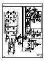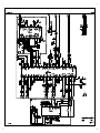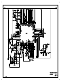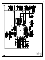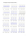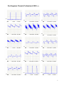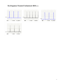
1
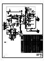
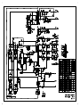
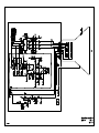
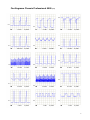
Service Manual
___________________________________________________________________________________
Chassis Professional 8000
___________________________________________________________________________________
Service notes
After a repair the cables must be laid out as originally fitted to save compliance with original approval
and to avoid failures or disturbances.
The mains cable prevents interference from the mains supply and is part of the product approval. For
replacement the original spare part only must be used.
Note di servizio
Dopo una riparazione i cavi devono essere disposti come posizionati all’origine per mantenere la
corrispondenza con le approvazioni originali ed evitare guasti o disturbi.
Il cavo di alimentazione previene interferenze provenienti dalla rete elettrica ed è parte delle
approvazioni del prodotto. Per la sostituzione deve essere utilizzato esclusivamente il ricambio
originale.
Modifications reserved - Con riserva di modifiche
Service procedure for Chassis Professional 8000
Power supply
Adjust PP1 for 140 V +/- 0.5 V across CP37.
Entering service mode
1. Turn on the appliance at the mains switch while holding down the MENU key on the
local control until the red LED lights up.
2. Release the MENU key on the local control and press the stand-by key on the remote
control. The appliance will start up in service mode with a specific support menu.
3. The various functions can be selected using the P+ and P- keys on the remote control
and the adjustment can be made using the Volume + keys. It is advisable to make a note of
the initial value before making the adjustment so that it can easily be restored if necessary.
If the memory NVM (ICR3) is replaced, it is essential to carry out all the adjustments
required in service mode because the replacement memory is supplied NOT preprogrammed. If the EPROM (ICR2) containing the software is replaced, compatibility with
the existing NVM is verified automatically and if necessary it is initialised. These
operations may take some time, so you must wait until they are completed.
Although the individual settings can be accessed and memorised individually and
independently, it is advisable to carry them out in the sequence in which they appear
when pressing the P- key.
Option byte
The correct value to be set for each appliance is marked on the label on the back of each item
alongside the writing Option byte. The value can be entered using the number keys on the
remote control.
AFC setting
Connect a generator (or a known transmitter of reliable quality) to the antenna input and use
the remote control number keys to enter the value of its RF frequency (which must be within
the frequency band indicated by the menu), then press OK. The setting will be made
automatically.
Repeat the procedure for BG, L and L’ standards. If any of the settings are omitted, operation,
automatic search and tuning in this standard may be incorrect.
AGC tuner setting
Connect a generator with an RF level of 1 mV (60 dBµV) (or a known transmitter of reliable
quality) to the antenna input and use the remote control number keys to enter the value of its
frequency (which must be within the frequency band indicated by the menu), then press OK.
The setting will be made automatically.
Screen grid voltage (Vg2)
Adjust the potentiometer G2 on the transformer EHT until the confirmation message appears.
No particular signal set-up is required.
Vertical geometry
The VS (Vertical Slope) function must be adjusted in such a way that the central horizontal
line in the test signal is exactly on the border between the visible image and the lower black
part. It must not subsequently be altered.
Now set the remaining parameters as accurately as possible in the sequence in which they
appear.
Horizontal geometry
Adjust as accurately as possible in the sequence in which they appear.
Adjusting white (Red/Green)
Using a B/W bar signal, adjust to obtain a grey image. The blue setting is fixed.
Exiting service mode
Once you have made the necessary adjustments, press the OK key on the remote control in
one of the menus in which it is active to memorise all the functions and return to normal
operation of the appliance.
Oscillograms Chassis Professional 8000 (1/5)
0V
0V
1
1 V/Div
10 µs/Div
0V
2
1 V/Div
10 µs/Div
3
1 V/Div
10 µs/Div
6
20 V/Div
10 µs/Div
9
100 V/Div
5 µs/Div
12
100 V/Div
5 µs/Div
15
1 V/Div
5 ms/Div
0V
0V
4
20 V/Div
10 µs/Div
0V
5
20 V/Div
10 µs/Div
0V
0V
0V
7
100 V/Div
8
5 µs/Div
5 V/Div
5 µs/Div
0V
0V
10
500 mV/Div
5 µs/Div
0V
11
2 V/Div
5 µs/Div
0V
0V
13
2 V/Div
10 µs/Div
14
500 mV/Div 10 µs/Div
0V
1
Oscillograms Chassis Professional 8000 (2/5)
0V
0V
0V
16
1 V/Div
10 µs/Div
0V
17
5 V/Div
10 µs/Div
0V
19
200 V/Div
10 µs/Div
18
2 V/Div
10 µs/Div
21
50 V/Div
10 µs/Div
0V
20
5 V/Div
5 ms/Div
0V
0V
0V
22
50 V/Div
23
5 ms/Div
10 V/Div
5 ms/Div
24
10 V/Div
10 µs/Div
27
50 V/Div
10 µs/Div
30
1 V/Div
10 µs/Div
0V
0V
25
50 V/Div
10 µs/Div
0V
0V
26
50 V/Div
5 ms/Div
0V
28
5 V/Div
10 µs/Div
0V
29
1 V/Div
10 µs/Div
2
Oscillograms Chassis Professional 8000 (3/5)
0V
0V
31
1 V/Div
0V
32
10 µs/Div
500 mV/Div 10 µs/Div
0V
33
500 mV/Div 10 µs/Div
0V
0V
34
500 mV/Div 10 µs/Div
35
1 V/Div
10 µs/Div
0V
1 V/Div
38
5 ms/Div
1 V/Div
5 ms/Div
39
1 V/Div
10 µs/Div
0V
0V
37
36
2 V/Div
10 µs/Div
0V
0V
40
2 V/Div
10 µs/Div
0V
41
200 mV/Div 50 ns/Div
43
500 mV/Div
10 µs/Div
2 V/Div
10 µs/Div
45
1 V/Div
20 µs/Div
0V
0V
0V
42
44
1 V/Div
20 µs/Div
3
Oscillograms Chassis Professional 8000 (4/5)
0V
46
0V
49
0V
1 V/Div
5 ms/Div
500 mV/Div 20 µs/Div
0V
47
500 mV/Div 20 µs/Div
50
500 mV/Div 20 µs/Div
0V
0V
52
1 V/Div
20 µs/Div
0V
0V
48
500 mV/Div 20 µs/Div
51
500 mV/Div 20 µs/Div
54
500 mV/Div 10 µs/Div
57
500 mV/Div 20 µs/Div
0V
53
500 mV/Div 10 µs/Div
56
500 mV/Div 20 µs/Div
0V
55
500 mV/Div 10 µs/Div
0V
0V
0V
58
500 mV/Div 20 µs/Div
0V
0V
59
1 V/Div
20 µs/Div
60
1 V/Div
5 ms/Div
4
Oscillograms Chassis Professional 8000 (5/5)
0V
0V
0V
61
1 V/Div
10 µs/Div
64
1 V/Div
5 ms/Div
62
1 V/Div
5 ms/Div
63
1 V/Div
10 µs/Div
0V
5
Chassis Professional 8000
Circuit description
Modifications reserved - Aenderungen vorbehalten - Con riserva di modifiche
1
Power supply
Consists of two completely separate sections:
• Stand-by power supply
• Main power supply
Stand-by power supply
This is an SMPS (Switch Mode Power Supply) operating at about 50 kHz with primary
side control and stabilisation performed by the integrated circuit VIPer20A (ICP10), which
provides exclusively the voltages required by the appliance in stand-by mode.
In these conditions the main power supply is completely deactivated, which allows for an
exceptionally low overall consumption (< 1 W), far lower than even the most stringent
standards.
The transformer TRP2 performs the dual function of isolating the appliance from the
mains power supply and generating on the secondary winding the supply voltage + 5 Vsb
which powers the IR receiver (IRH1), the microcontroller (ICR1), the NVM memory (ICR3),
the reset circuit (ICR6) and the EPROM (ICR2) containing the software. A duplicator
circuit is used to obtain a voltage of about 20 V used for turning off the electromagnetic
mains switch (optional).
Main power supply
This is an SMPS (Switch Mode Power Supply) operating at about 45 kHz with secondary
side control and stabilisation performed by the integrated circuit TEA2262 (ICP1).
The transformer TRP1 performs the dual function of isolating the appliance from the
mains power supply and generating the correct supply voltages on the various secondary
windings.
In stand-by the TRIAC DP2 does not conduct, so the circuit (including the PTC powering
the degaussing coil) is completely disconnected from the power supply and therefore has
no power consumption.
When it is turned on by means of the photo-coupler ICP3, the TRIAC DP2 is made to
conduct and the rectified and smoothed mains voltage across CP14, via winding 5/2 of
transformer TRP1, is present on the collector of TP1, which does not conduct because
ICP1 is not yet powered.
Simultaneously CP16 is charged from mains via RP3. As soon as the voltage across it
reaches a value of about 10 V, the integrated circuit begins to operate and generates on
pin 14 the driving pulses for making transistor TP1 conduct.
Current therefore begins to flow in the primary winding 5/2 of the transformer and across
the winding 1/7 there are formed pulses which are rectified by DP4 and smoothed by
CP16 and ensure a complete power supply of ICP1.
At the same time currents are also induced in the secondary windings; after being rectified
and smoothed these currents generate the various power supply voltages.
A voltage taken from across CP37 by way of the voltage divider made up of
RP35/RP29/RP23/RP33/PP1 is applied to the base of TP4 and causes a proportional
current to flow in the photodiode contained in the optocoupler ICP2.
2
This value is transferred via the photo-coupler emitter to the input (pin 6 of ICP1) of a
comparator which regulates the duration of the base drive pulses of transistor TP1.
This controls the time for which current is allowed to flow in the primary winding (and
therefore regulates the energy fed into the transformer) and gives extremely precise
stabilisation of the voltages available on the transformer’s secondary windings.
The circuit made up of CP24/CP25/LP10/DP6 controls the current harmonics towards the
mains power supply and may be present or absent depending on applicable regulations.
This solution activates automatic demagnetisation of the CRT every time the appliance is
turned on, not just from the switch but also from stand-by. This solves the problem of
possible purity degradation if the appliance (as often happens) is not turned off regularly
from the mains switch.
Protection
To protect against supply voltage variations, the integrated circuit ICP1 interrupts
generation of driving pulses to pin 14 if the voltage at pin 16 is higher than about 15.5 V.
Furthermore the current that flows in the transistor TP1 is read across RP9 and is applied
to pin 3 via RP5/RP14; if it exceeds the maximum permitted value, the driving pulses to
pin 14 are interrupted.
This protects the transistor TP1 and safeguards against short-circuits in the transformer’s
secondary windings.
Microcontroller
A latest-generation device with 16-bit architecture (ICR1 - M30612SFP) is used,
supported by an EPROM (Electrically Programmable Read Only Memory) that contains all
the appliance software.
The various functions are controlled either by changing the logic state (L or H) of some
pins on the microcontroller or by way of a two-wire digital bus (pins 27/28) designated IICbus (Inter Integrated Circuit Bus).
An additional IIC-bus (pins 91/92) is devoted exclusively to dialoguing with the NVM
memory (Non Volatile Memory) (ICR3) to provide maximum protection against data
corruption.
Connected to pins 32/33/34 there is also a special high-speed M3-L bus dedicated
exclusively to dialoguing with ICR5 (SDA5273-2P) for managing teletext and graphic
OSDs (On Screen Displays).
The signal from the IR receiver is applied to pin 7 of the microcontroller, which begins its
activity when the supply voltage is present and the reset cycle (active L) at pin 12 has
been completed.
For this reason if the system shows abnormal behaviour it is important to turn the power
switch off and back on again to generate a reset pulse allowing the program to be
reinitialised.
3
When the reset pulse has terminated, the microcontroller waits until the control signals
from IR are present at pin 7 or those from the local control are present at pin 97.
Execution of the entire program is timed by the clock signal generated by the 10 MHz
crystal and applied to pins 13/15.
A valid command for exiting standby generates a level L at output pin 100, thereby
enabling powering up of all the circuits as described in the power supply section.
The microcontroller first verifies that the power supply has come on correctly by checking
that pin 18 (START) is at level H, then all the possible peripherals are interrogated via the
IIC-Bus to recognise the configuration of the appliance and thereby structure the program.
All data regarding the operating parameters required for correct setting of all the functions
(tuning, analogue values, geometries, option bytes, etc.) are subsequently called up from
the memory ICR3.
The various functions are carried out and commands given primarily via the digital buses.
The functions of the remaining microcontroller pins are described below:
Pin 1 - Output (LPW) which goes to level L during the main power supply start-up to
activate initial operation of the horizontal deflection stage.
Pins 3/4 - DAC (Digital to Analog Converter) outputs for headphone volume and balance
control.
Pin 19 – Input connected to vertical flyback pulse used for managing communication
timing with 100 Hz processor.
Pin 20 – Output which goes to level H to activate audio power amplifier muting.
Pin 21 – Output for controlling satellite antenna system switching.
Pins 24/25 – Inputs for automatically recognising the configuration of the 100 Hz
conversion system.
Pin 26 – Input for automatically recognising correspondence of deflection hardware used.
Pin 30 – Input for automatically recognising the presence of the Comb filter.
Pins 35/36/37 – Outputs reserved for future use.
Pin 38 – Output for controlling loudspeaker configuration in Dolby Pro Logic mode.
Pin 89 – Input used for controlling VGA input enabling.
Pin 93 – Output for controlling illumination of local control LED.
Pin 94 – Output for controlling activation of electromagnetic switch (if present).
Pin 95 – Input connected internally to an ADC (Analog to Digital Converter) to measure
the value of the tuner’s AGC voltage.
4
Pin 97 – Input connected internally to an ADC (Analog to Digital Converter) to measure
the value of the voltage generated by the local control keys and hence discriminating the
control.
Note that the software also identifies the configuration of the appliance by way of an
option code contained in the memory ICR3. This option code must therefore be checked
and if necessary adjusted if ICR3 is replaced. The correct value for each model is marked
on the label on the back of each item after the words “option code”. It can be set by
entering service mode (follow the necessary safety procedures).
In this mode it is also possible to make all the adjustments for the various calibrations
under the control of a specific program contained in the microcontroller, which also verifies
automatically whether NVM data initialisation operations are required.
NVM memory (ICR3)
This is an EEPROM (Electrically Erasable Programmable Read Only Memory) NVM (Non
Volatile Memory) with a 16K bit capacity and an IIC-bus interface.
The microcontroller writes and reads all the variable data relevant to operation in the
memory.
In addition to user option data (tuning, analogue levels, etc.), memory ICR3 also contains
data regarding the settings of many of the appliance’s functions, such as geometries,
option bytes, white level adjustment, etc.
If the memory is replaced, these settings must be restored through the appropriate
service procedures.
However, the program contains special check routines so the appliance can be turned on
when the memory is not programmed or even not present, thereby simplifying the service
procedures.
Video signal processing / deflection
The various items of information in the video signal are processed by the integrated
circuits TDA9321H (ICC2), TDA9332H (ICC1) and SAA4977H (ICY1).
• TDA9321H
5
Video
The IF signal from the tuner whose band is limited by the surface wave filter FCC5 is
routed to pins 2/3, which are connected to the input of the video demodulator
(synchronous PLL type with active carrier regeneration). This assures ultralinear
demodulation, an excellent demodulation figure, a low harmonic content and an excellent
impulsive response.
The only residual adjustment that must be carried out on the video demodulation circuits
is tuning of coil LC9 of the VCO oscillator and setting the working point of the tuner AGC,
which is controlled by way of pin 62. Both the adjustments are performed fully
automatically by the software in service mode.
The baseband video signal is available with an amplitude of 2 Vpp at pin 10 and is applied
via the audio carrier suppression filter FCC3 to pin 12, which represents the input of the
group delay correction circuit controlled by software.
After this treatment the signal is available at pin 13 with an amplitude of 2 Vpp.
From here it is sent both to the SCART 1 output and to one of the video selector inputs
(pin 14) after being taken to the level of 1 Vpp.
Further video inputs are available at pins 16 (AV1), 18 (SAT), 20 (AV2) and 23 (FRONT).
S-VHS sources whose chrominance signals are connected to pins 21 and 24 can also be
connected to the AV2 and FRONT inputs respectively.
The video signal of the selected source is taken from pin 26 to power the teletext decoder.
In order to send the selected signal to the screen, it is routed internally through a bandpass filter to remove the chrominance signal and a trap to eliminate the colour subcarrier
from the luminance signal.
In the case of SVHS sources these circuits are bypassed.
Switched capacitance circuits are also included for creating luminance delay lines.
The chrominance signal is demodulated in accordance with the PAL/SECAM/NTSC
standard identified automatically and with the aid of integrated delay lines. The carrier
reconstruction oscillators are connected to their respective crystals via pins 54 and 57.
Original spare parts must be used for these components as all the functions of the
integrated circuit take their frequencies as reference.
After the treatments described above, the luminance signal Y50 and the colour difference
signals U50, V50 are available on pins 49, 50 and 51 respectively.
There are also two video outputs which can be freely connected to any of the inputs and
are used for the SCART2 output (pin 34) and for the PIP module (pin 32).
Pins 25, 26, 27, 28, 29 and 30 are used for connection to an optional comb-filter. The
SCART1 RGB input is connected to pins 40, 41, 42 and 43 and the PIP source Y/U/V
signals to pin 36, 37, 38, 39.
Pins 19 and 22 are outputs which can be placed in an H or L level under the control of the
software and are used respectively for L/L’ switching of the audio filter FCC4 and for
switching of the video signal output on SCART1 by means of the transistors TW3, TW4,
TW5, TW6, TW7 and TW8.
Audio
The IF signal from the tuner whose band is limited by the surface wave filter FCC4 is
routed to pins 63/64, which are connected to the mixer consisting of a multiplier which
6
converts the IF signal to the intercarrier frequency. This frequency is available at pin 5
after a high-pass filter which eliminates the video content.
The is also an AM audio demodulator whose output is also connected to pin 5.
Deflection
The horizontal and vertical synchronising signals are extracted from the screen video
signal.
The horizontal synchronising pulse HA is available at pin 60, the vertical synchronising
pulse VA at pin 61 and the sandcastle pulse at pin 59.
• SAA4977H (1fH / 2fH converter)
The signals Y50, U50, V50 coming from ICC2 are connected to input pins 26, 28 and 30,
while the horizontal HA and vertical VA synchronising signals are connected to pins 22
and 20 respectively.
To double the field frequency (100 Hz) it is necessary to write the same original field twice
on the screen.
For this purpose, the incoming video signals are first digitalised by sampling them at 8 bits
and then transferred to a memory (ICY4), from which they are read at double speed.
Digital to analog reconversion is then performed and the double-frequency analog signals
are available at pins 79, 76 and 74. The circuits formed by TY1/TY2, TY3/TY4 and
TY5/TY6 adapt the levels for the ICC1 inputs.
It is also necessary to generate the HD/VD synchronising pulses at double frequency and
synchronous to those of the original HA/VA signal.
This is done with the help of the PLL circuit made up of ICY2 and ICY3.
All checks and signals needed for the various functions and for memory management are
inside ICY1, which also contains a microcontroller and resident software to carry out the
various activities. The transistors TY8/TY9 form the reset circuit for this microcontroller.
The integrated circuit ICY9 switches the synchronising signals between the internal
source (pins 2 and 5) and the VGA input (pins 3 and 6). Switching is controlled by pin 3 of
ICY1.
The integrated circuit ICY5 (if present) increases the definition by acting on the signal’s
transient fronts.
• TDA9332H
Video
Signals Y100, U100 and V100 from the 100Hz conversion module are connected to pins
26, 27 and 28.
The RGB signals for performing saturation, contrast and brightness controls are restored
by way of the matrix circuits. The signals for driving the video final amplifiers are therefore
available on output pins 40, 41 and 42.
Pin 44 is the input for the measurement pulses for adjusting the cut-off, which uses an
automatic system for alignment at both low and high current, thereby optimising the
7
performance of the tube. Adjustment of voltage Vg2 is fully automated in service mode by
a special software procedure.
Pin 43 is the control input for automatic limitation of the tube current.
Pins 35, 36, 37 and 38 are the inputs of the RGB signals for the OSD and teletext, while
pins 30, 31, 32 and 33 are the RGB inputs of the VGA source. These inputs require
sources with a horizontal frequency of 32 kHz.
Deflection
The entire management of the deflection controls refers to the 12 MHz oscillator FCC1
connected to pins 20/21.
When turned on, the transistor TC3 is made to conduct by pin 1 of microcontroller ICR1,
thereby powering pin 22. This activates the output of horizontal driving pulses from pin 8
at a frequency of about 50 kHz. This starts the horizontal deflection stage, whose
consumption permits stabilisation of the power supply.
When the power supply voltage on pins 17/39 reaches 8V, the horizontal driving output
progressively switches to its rated frequency (32 kHz) and the steady-state operating
mode is reached. The software now disconnects the power supply voltage from pin 22.
The transistor TC4 is normally inhibited because its base, via RC34, is connected to earth
by the jumper JF1 situated on the power supply/deflection circuit and this level L is also
carried to pin 26 of the microcontroller. This also allows the correct operating frequency of
ICC1 (H = 32 kHz; L = 15 kHz) to be provided via pin 12, which also depends on the
deflection hardware used.
The horizontal HD and vertical VD synchronising pulses are applied to input pin 24 and 23
respectively.
Pin 13 is the input of the horizontal flyback pulse and pin 4 is the input for dimensional
stabilisation of the image as the tube current varies.
Pin 9 is used as input to protect the tube, blancking it out in the event of a fault in the
vertical deflection circuits.
Pins 1 and 2 are the symmetrical outputs for vertical driving and pin 3 is the output for
E/W correction control.
All the adjustments are performed in service mode by a special support software program.
Video final amplifiers
The RGB signals available at pins 40/41/42 on ICC1 (TDA9332H) must be amplified and
inverted in order to reach the level required for driving the CRT.
The integrated circuit TDA6108 (ICV1) is used for this purpose.
The final amplifier inputs are connected to pins 1/2/3 and the outputs (pins 7/8/19) are
connected directly to the CRT’s cathodes via the protection resistors RV5/RV7/RV10.
A copy of the currents flowing in the CRT’s cathodes are available at pin 5 and this
information is sent to the video processor TDA9332H for automatic cut-off control circuit
operation.
8
Transistors TV1 and TV4 form a circuit which serves to eliminate CRT spot formation when
the appliance is turned off.
During operation the heater’s supply pulses, which are rectified and filtered by DV6 and CV6,
keep TV1 saturated and hence inhibit TV4.
The capacitor CV19 is therefore able to charge up at the voltage of +200V by way of RV19
and DV10. Grids 1 (G1) of the tube remain at ground potential since DV10 is conducting.
As soon as the appliance is turned off, the final line stage stops providing the heater’s power
supply pulses; TV1 is inhibited and TV4 is saturated by the +200V voltage still present and
applied at its base via RV18.
The collector of TV4 grounds the positive armature of CV19. As a result, grids 1 of the CRT
are polarised with the negative 200V voltage present on its negative armature since the diode
DV10 is now polarised the other way round.
This way the CRT is completely inhibited for the time it takes CV19 to discharge, thus
preventing spot formation.
The RGB signals, decoupled by means of the transistors TV7/TV8/TV9, are added
together and transferred to the power stage made up of TV5 and TV6 by means of the
circuit made up of TV2 and TV3. The coupling capacitor CV13 together with the power
stage input impedance forms a differentiator circuit which generates pulses of suitable
polarity upon each signal transition. This drives a special deflection coil on the CRT which
modulates the deflection velocity (Beam Velocity Modulation), thereby significantly
improving image definition.
Horizontal deflection
The output line transistor is driven by the transformer TRL1 whose primary winding is
driven by the transistor TL1, connected to the horizontal drive output of ICC1 via the
emitter-follower TC5.
The horizontal deflection stage is carried out in a conventional manner with the deflection
transistor TL2, the diode (DL4/DL5) EW modulation circuit and pin-cushion distortion
correction (CL8/LL6). The correction signal EW is injected into the central point of the
diodes via LG2.
The capacitive divider formed by CL11/CL12 is used for picking up the horizontal flyback
pulse to be applied to pin 13 of ICC1, limiting its maximum value to 8V by means of the
diode DL11.
Vertical deflection – EW correction
9
These functions are performed by the integrated circuit TDA8351 (ICF1). This is a power
amplifier with a bridge output that allows the vertical deflection coils to be connected
directly to pins 4 and 7. The resistances RF9/RF10, which provide pin 9 with the
necessary feedback signal, are placed in series.
The differential input circuit (pins 1/2) is driven by the voltage formed across RF3/RF4 for
the symmetrical driving currents provided by ICC1.
Pin 8 is an output which switches to the value H at vertical flyback. This signal is
connected to pin 9 of ICC1 and is used to protect the CRT in the event of failure of the
vertical deflection circuits.
Two separate supply voltages are used for the deflection part (pin 3) and for generating
the flyback pulse (pin 6), thereby achieving a high value of efficiency.
The power stage for EW correction consists of transistor TG1 which is driven directly by
ICC1 and whose collector is connected to the injection coil LG2 by means of RG4.
Audio signal processing
The various audio functions are treated by the circuits TDA9870/5A (ICS1), SAA7710T
(ICS4), TDA7467D (ICS5), TDA2616 (ICS2/ICS6), TDA7053AT (ICS3).
• TDA 9870A / TDA 9875A
The integrated circuits have the same basic functions: the version TDA9875A additionally
contains a complete NICAM digital audio decoder.
The audio IF signal from pin 5 of ICC2 is applied to input pin 12. The AM audio signal (in
the case of L/L’ standard) is also extracted by way of the transistor TS1 and the low-pass
filter formed by RS34 and CS13 and is taken to input pin 29. A second IF input (pin 10) is
used for the audio signal of the satellite receiver (if present).
All audio functions (demodulation, stereo/NICAM decoding, input/output switching,
volume/tone control, effects) for BG/DK/I/LL’ standards are contained in the integrated
circuit and are totally selected and controlled via software.
The audio inputs from the SCART 1 and SCART 2 sockets are connected to pins 33/34
and 36/37 respectively, while the audio input from the front RCA sockets (optional) is
connected to pins 31/32.
10
Pins 47/48 and 51/52 are the outputs towards the SCART 1 and SCART 2 sockets
respectively.
Pins 62/63 are the constant level outputs for the LINE OUT sockets, fed by the transistors
TW11 and TW13; pins 60/61 are the outputs for the loudspeaker power amplifiers (ICS2).
Pins 22/23/25/26/27 are the inputs/outputs of the I2S digital bus used for communications
with ICS4 (present only in Dolby Pro Logic appliances).
• SAA 7710T
This is present only in appliances equipped with Dolby Pro Logic decoding and also
provides the function of a 5-band audio equaliser.
Signal treatment is fully digital and data transfer to and from ICS1 is performed via the bus
I2S which is connected to pins 22/23/24/28/29.
A specific software program is responsible for complete management of all functions,
including a special spatial sound (Incredible Sound) which offers effects similar to Pro
Logic decoding without the need to install rear loudspeakers.
• TDA 7467D
ICS5 can be used as an alternative to the Dolby Pro Logic decoder ICS4. This creates
special spatial sound effects while using solely the loudspeakers contained in the
appliance.
The input signal to be processed is connected to the pins 2/3 and the outputs are
connected to pins 1/28. It is fully managed by software.
• TDA 2616
This is a double Hi-Fi audio power amplifier in accordance with DIN45500.
ICS2 is always present, whereas ICS6 is used solely in Dolby Pro Logic appliances to
amplify the central and rear channels.
The input signals are connected to pins 1/9 and the outputs to pins 4/6.
Pin 2 mutes the amplifiers and is controlled via the transistor TW9.
The transistors TW12 and TW14 activate MUTE during power supply transients.
The right and left channel signals are also added together and sent, via the transistor
TW10, to the woofer box amplifier (present in some models only).
• TDA 7053AT
This is a double amplifier used to power the headphone socket.
The inputs are connected to pins 4/6 and the outputs to pins 9/16. The reproduced signal
is the same as that of the loudspeakers and its volume and balance can be controlled by
way of pins 2/8 connected to the output pins 3/4 of microcontroller ICR1.
11
Woofer amplifier
This is present in some models only and is used to power the woofer loudspeaker box.
The integrated circuit LM358N (ICB1A/B) constitutes a two-stage low-pass filter in
cascade and serves to eliminate all frequencies higher than about 300 Hz from the audio
signal spectrum.
Power amplification is performed by the integrated circuit TDA2616 (ICB2) connected in a
bridge configuration, which directly powers the box loudspeaker.
The circuit made up of the transistor TB2 and the relay RLB1 is used solely in Dolby Pro
Logic appliances to adapt the internal loudspeaker connections according to the
installation configuration chosen by the user from the OSD menu.
Switching is managed by pin 38 of the microcontroller, which directly drives the base of
TB2.
VGA interface
This option (present only on some models) allows the appliance to be used as a computer
monitor at the following VGA resolutions only:
pixel
horizontal
vertical
640x480
640x350
640x400
31.5 kHz
31.5 kHz
31.5 kHz
60 Hz
70 Hz
70 Hz
The PC’s graphic interface must be set for these resolutions.
The RGB video signals are sent directly to the input pins 30/31/32 of ICC1 while the
synchronising signals from pins 13 and 14 of CNM1 are applied to the integrated circuit
ICM1 (Quad.2-input exclusive-OR) which provides positive pulses to output pins 3/6
whatever the input polarity. This way the appliance is automatically adapted to any type of
PC.
The presence of horizontal and vertical synchronising pulses is checked by means of
ICM2, whose output pins 6 and 10 are at level H only if the horizontal and vertical
synchronising pulses respectively are present.
Only in this case can pin 2 of CNM3 (VGA ENABLE) go to level H.
The integrated circuit ICM3 is used to check that the frequency of the horizontal
synchronising pulses is lower than the maximum value set by PM1 to prevent an incorrect
PC resolution setting damaging the television’s horizontal deflection stages.
Potentiometer PM1 is factory-set. It requires special equipment for adjustment and
its setting must not be altered.
12
If the value of the horizontal frequency is not correct, pin 10 of ICM3 is kept at level L and
consequently the communication line with the microcontroller (VGA ENABLE) goes to
about 2.5 V. This information is used to generate a specific error message.
The integrated circuit ICM4 switches between VGA and front RCA audio sources and the
transistors TM1/TM2/TM3/TM4 adapt the VGA audio level to that inside the TV set.
13
Spare parts list
Lista parti di ricambio
Chassis Professional 8000
Rev 1.2
Part.No.
Codice
Ref./pos
Description
Descrizione
S000558000
Front End PCB 8000 cpl.
S000558750
Front End PCB 8000 Nicam/Dolby cpl. Base Front End 8000 Nicam/Dolby cpl.
S000558500
Front End PCB 8000 Nicam cpl.
Base Front End 8000 Nicam cpl.
S000558250
Front End PCB 8000 Dolby cpl.
Base Front End 8000 Dolby cpl.
!
S047501000
Fusible resistor 1 Ohm
Resistenza sicurezza 1 Ohm
!
S047502200
Fusible resistor 2,2 Ohm
Resistenza sicurezza 2,2 Ohm
!
S047504700
Fusible resistor 4,7 Ohm
Resistenza sicurezza 4,7 Ohm
S055408020
Wire wound resistor 1 Ohm 7W
Resistenza a filo 1 Ohm 7W
S061112050
Diode BAS 32 L
Diodo BAS 32 L
DC4/DC5
S061517920
Diode BA792/T1
Diodo BA792/T1
ZC4
S061518100
Diode BAS81
Diodo BAS81
ZR1
S061703300
Zener diode 3V3
Diodo zener 3V3
ZC3
S061706800
Zener diode 6V8
Diodo zener 6V8
ZC5
S061713300
Zener diode 33V
Diodo zener 33V
S062608500
Transistor BC 847 B
Transistor BC 847 B
S062608600
Transistor BC 857 B
Transistor BC 857 B
ICS2/ICS6
S063126160
I.C. TDA 2616/N1
I.C. TDA 2616/N1
ICS1
S063198700
I.C. TDA 9870A (no Nicam)
I.C. TDA 9870A (no Nicam)
ICS1
S063198750
I.C. TDA9875A V2 (Nicam)
I.C. TDA 9875A V2 (Nicam)
ICR3
S063286160
I.C. EEPROM M24C16-BN6
I.C. EEPROM M24C16-BN6
ICR2
S063342700
I.C. EPROM M27C4001-80XF1
I.C. EPROM M27C4001-80XF1
ICR4
S063344400
I.C. MSM514400D-60
I.C. MSM514400D-60
ICR1
S063362060
I.C. M30612SFP
I.C. M30612SFP
ICR6
S063363190
I.C. M51953BFP
I.C. M51953BFP
ICS4
S063377100
I.C. SAA 7710T/N104/T3 (Pro Logic only)
I.C. SAA 7710T/N104/T3 (Pro Logic solo)
ICR5
S063552730
I.C. SDA 5273 2P
I.C. SDA 5273 2P
ICS3
S063570530
I.C. TDA 7053AT/N2,118
I.C. TDA 7053AT/N2,118
ICC2
S063593200
I.C. TDA 9321H/N1/T3
I.C. TDA 9321H/N1/T3
ICC1
S063593310
I.C. TDA 9332H/N1/T3 1Y
I.C. TDA 9332H/N1/T3 1Y
ICC1
S020030000
I.C. TDA 9332H/N2/T3 2Y
I.C. TDA 9332H/N2/T3 2Y
QC4
S066900150
Quarz 3,58 Mhz
Quarzo 3,58 Mhz
QC1
S066900250
Quarz 4,43 Mhz
Quarzo 4,43 Mhz
QR1
S066900400
Quarz 10 Mhz
Quarzo 10 Mhz
QR2
S066902040
Quarz 20,48 Mhz
Quarzo 20,48 Mhz
QS1
S066902450
Quarz 24,576 Mhz
Quarzo 24,576 Mhz
RW46
Base Front End 8000 cpl.
Pagina 1
NOTE
QS2
S066903680
Quarz 36,864 Mhz
Quarz 36,864 Mhz
FCC5
S067322000
SAW Filter K3953M
Filtro SAW K3953M
FCC4
S067322500
SAW Filter K9453M
Filtro SAW K9453M
FCC1
S067330610
Ceramic resonator CSTCS 12.0MT
Risuonatore ceramico CSTCS 12.0MT
FCC3
S067401050
Ceramic filter TPS 5,5 MWA
Filtro ceramico TPS 5,5 MWA
LC9
S067408200
Coil P3691NAS-A41
Bobina P3691NAS-A41
TUC1
S069023200
Tuner UV 1316 AI2
Tuner UV 1316 AI2
PLS1/PLS2
S071013400
Ext. Speaker connector
Presa x altop. esterno
SC1/SC2
S071014800
Double SCART connector
Presa SCART doppia
CNS6
S071015400
Line out RCA connector
Presa RCA line out
S087170000
Chassis holder side
Staffa supporto telaio
S087178100
Chassis rear connector cover
Sfondo posteriore
S087178500
Chassis holder front
Supporto telaio anteriore
S000568500
Power PCB 8000 4:3 25" PH cpl.
Modulo Power 8000 4:3 25" PH cpl.
S000568510
Power PCB 8000 4:3 28" PH cpl.
Modulo Power 8000 4:3 28" PH cpl.
S000568520
Power PCB 8000 4:3 29" PH cpl.
Modulo Power 8000 4:3 29" PH cpl.
S000568530
Power PCB 8000 4:3 34" VI cpl.
Modulo Power 8000 4:3 34" VI cpl.
S000568800
Power PCB 8000 16:9 28" VI cpl.
Modulo Power 8000 16:9 28" VI cpl.
S000568810
Power PCB 8000 16:9 32" VI cpl.
Modulo Power 8000 16:9 32" VI cpl.
S000568820
Power PCB 8000 16:9 28" PH cpl.
Modulo Power 8000 16:9 28" PH cpl.
!
S044010100
Fusible resistor 1 Ohm NFR25
Resistenza sicurezza 1 Ohm NFR25
!
S044010470
Fusible resistor 4,7 Ohm NFR25
Resistenza sicurezza 4,7 Ohm NFR25
!
S048002200
Fusible resistor 2,2 Ohm NFR25H
Resistenza sicurezza 2,2 Ohm NFR25H
!
S048033000
Fusible resistor 33 Ohm NFR25H
Resistenza sicurezza 33 Ohm NFR25H
!
S048147000
Fusible resistor 470 Ohm NFR25H
Resistenza sicurezza 470 Ohm NFR25H
RP1
!
S053051000
Safety resistor 1MOhm VR37
Resistenza 1 MOhm VR37
RP38
!
S053210700
Safety resistor 4M7Ohm VR68
Resistenza 4M7 Ohm VR68
S054000150
Wire wound resistor 0,15 Ohm 3W
Resistenza a filo 0,15 Ohm 3W
S054001000
Resistor 1 Ohm 2W
Resistenza 1 Ohm 2W
S054004700
Resistor 4,7 Ohm 2W
Resistenza 4,7 Ohm 2W
RF11
S054115000
Resistor 150 Ohm 2W
Resistenza 150 Ohm 2W
RP3
S054347000
Resistor 47 KOhm 2W
Resistenza 47 KOhm 2W
RP16
S055492270
Resistor 27 KOhm 7W
Resistenza 27 KOhm 7W
NTC1
S056590200
NTC resistor 4,7 Ohm
Resistenza NTC 4,7 Ohm
S056591100
PTC resistor 12A
Resistenza PTC 12A
S061002100
Diode BAV 21/A52A
Diodo BAV 21/A52A
S061111320
Diode 1N 4007
Diodo 1N 4007
S061112050
Diode BAS 32L
Diodo BAS 32L
S061281050
Diode BAV 203-GS18
Diodo BAV 203-GS18
S061301360
Diode BYW 36
Diodo BYW 36
S061401370
Diode BYD 37K/T1
Diodo BYD 37K/T1
S061503750
Diode BYD37J,115
Diodo BYD37J,115
RP9
PTC1
DF1
!
Pagina 2
DP16/DP24
S061706200
Zener diode 6V2
Diodo zener 6V2
ZF1/ZL1
S061909350
Zener diode BZT03-C51/A52A
Diodo zener BZT03-C51/A52A
ZP1
S061703300
Zener diode 3V3
Diodo zener 3V3
DP20
S061011000
Bridge rectifier B250D
Diodo ponte B250D
DP1
S061270000
Bridge rectifier B380C3200-2200
Diodo ponte B380C3200-2200
DP10
S061299080
Diode BYW 80PI-200
Diodo BYW 80PI-200
DP5/DP8
S061299120
Diode BYT 12PI-1000
Diodo BYT 12PI-1000
S061303800
Diode BYV 98-200
Diodo BYV 98-200
DL10
S061316870
Diode BY 228
Diodo BY 228
DL5
S061316900
Diode BY 229F-800
Diodo BY 229F-800
DL4
S061319200
Diode BY 459X-1500
Diodo BY 459X-1500
DP2
S061401480
Triac BTA 08-700CW
Triac BTA 08-700CW
TL1
S062520300
Transistor BC 635-16
Transistor BC 635-16
S062608500
Transistor BC 847 B
Transistor BC 847 B
S062608600
Transistor BC 857 B
Transistor BC 857 B
TP1
S062756700
Transistor STH 7NA80 FI
Transistor STH 7NA80 FI
TL2
S062764100
Transistor BUH 1015 HI
Transistor BUH 1015 HI
TG1
S062815480
Transistor STP 12NB30FP
Transistor STP 12NB30FP
ICP1
S063164520
I.C. TEA 2262
I.C. TEA 2262
ICP9
S063249500
I.C. LE 50CZ AP
I.C. LE 50CZ AP
ICP3
!
S063410300
I.C. K 3023 P
I.C. K 3023 P
ICP2
!
S063411010
I.C. TCD T 1102 GB
I.C. TCD T 1102 GB
ICF1
S063183510
I.C. TDA 8351/N6
I.C. TDA 8351/N6
ICP4
S063209700
I.C. L 78S05/CV
I.C. L 7808CV
ICP7
S063210500
I.C. L 7808CV
I.C. L 7808CV
ICP6
S063210520
I.C. L 7812CV
I.C. L 7812CV
ICP10
S063240000
I.C. VIPER 20A DIP
I.C. VIPER 20A DIP
FP1/FP4/FP5 !
S070503900
Fuse T2,5A
Fusibile T2,5A
FP3
!
S070503940
Fuse T4A
Fusibile T4A
FP7
!
S070504000
Fuse T315 mA
Fusibile T315 mA
FP2
!
S070506500
Fuse T 3,15A
Fusibile T 3,15A
CP17
S017120000
Condensator 220 pF 1000V
Condensatore 220 pF 1000V
CP23
S020222000
Condensator 2K2 pF 4000V
Condensatore 2K2 pF 4000V
CP73
S040780100
Condensator 10 µF 385V
Condensatore 10 µF 385V
CP14
S040781500
Condensator 150 µF 385V
Condensatore 150 µF 385 V
TRL2
!
S065624000
Flyback transformer
Trasformatore EAT
TRL2
!
S031010010
Flyback transformer (Dynamic focus)
Trasformatore EAT (Dynamic focus)
TRP2
!
S065701100
Stand-by transformer
Trasformatore Stand-by
TRP1
!
S065706100
Power supply transformer
Trasformatore di alimentazione
TRP3
!
S066541750
Mains filter
Filtro rete
TRL1
S066548000
Line driver transformer
Trasformatore di riga
LG2
S067070800
E/W Coil
Bobina E/W
LL6
S030040020
Bridge Coil
Bobina ponte
Pagina 3
LG1
S067081440
Linearity coil
Bobina linearità
S067419000
Choke 110 µH
Choke 110 µH
S000678510
RGB PCB cpl. (PHILIPS CRT)
Modulo RGB cpl. (cinescopio PHILIPS)
S000678500
RGB PCB cpl. (VIDEOCOLOR CRT)
Modulo RGB cpl. (cinescopio VIDEOC)
S054001000
Resistor 1 Ohm 2W
Resistenza 1 Ohm 2W
S061002100
Diode BAV 21/A52A
Diodo BAV 21/A52A
DV10
S061111320
Diode 1N 4007
Diodo 1N 4007
DV6
S061112050
Diode BAS 32 L
Diodo BAS 32 L
DV4/DV8
S061281050
Diode BAV 203-GS18
Diodo BAV 203-GS18
TV6
S062528230
Transistor BD 230/B
Transistor BD 230/B
TV5
S062528240
Transistor BD 231/B
Transistor BD 231/B
TV4
S062607200
Transistor BF 720,115
Transistor BF 720,115
S062608500
Transistor BC 847 B
Transistor BC 847 B
S062608600
Transistor BC 857 B
Transistor BC 857 B
TV2/TV3
S062620000
Transistor BSV52,215
Transistor BSV52,215
ICV1
S063161080
I.C. TDA 6108JF/N1
I.C. TDA 6108JF/N1
CNV2
S070001200
CRT socket
Zoccolo cinescopio
S000530210
100Hz Features PCB cpl.
Modulo Features 100Hz cpl.
S061112050
Diode BAS 32 L
Diodo BAS 32 L
DY2
S061500400
Diode BBY40/T1
Diodo BBY40/T1
DY3
S061515500
Diode BZV55C3V6
Diodo BZV55C3V6
DY1
S061518010
Diode BAS16/T1
Diodo BAS16/T1
TY7
S062605500
Transistor BF 550/T1
Transistor BF 550/T1
S062608500
Transistor BC 847 B
Transistor BC 847 B
S062608600
Transistor BC 857 B
Transistor BC 857 B
ICY6/ICY8
S063209600
I.C. L 78L05ACZ AP
I.C. L 78L05ACZ AP
ICY4
S063349550
I.C. SAA 4955TJ/V1/T3
I.C. SAA 4955TJ/V1/T3
S020020000
I.C. SAA 4956TJ/V1/T3
I.C. SAA 4956TJ/V1/T3
ICY1
S063349770
I.C. SAA 4977H/V1/T3
I.C. SAA 4977H/V1/T3
ICY2
S063367400
I.C. M74HCT 04
I.C. M74HCT 04
ICY9
S063367420
I.C. M74HCT 157
I.C. M74HCT 157
ICY7
S063549310
I.C. L4931-CDT33
I.C. L4931-CDT33
ICY3
S063574400
I.C. 74 HCT4046AD/T3
I.C. 74 HCT4046AD/T3
LY4
S067407900
Coil A638AN-0164Z
Bobina A638AN-0164Z
S000768000
VGA PCB cpl.
Modulo VGA cpl.
S062608500
Transistor BC 847 B
Transistor BC 847 B
S062608600
Transistor BC 857 B
Transistor BC 857 B
ICM4
S063574000
I.C. 74 HC 4053D,653
I.C. 74 HC 4053D,653
ICM1
S063574080
I.C. 74 HCT86 D
I.C. 74 HCT86 D
ICM2/ICM3
S063574450
I.C. 74 HCT4538D
I.C. 74 HCT4538D
RV40
Pagina 4
CNM7
S071020100
RCA connector withe
Presa RCA bianca
CNM6
S071020110
RCA connector red
Presa RCA rossa
CNM1
S071040150
VGA connector
Connettore VGA
S000868100
Audio Booster PCB cpl.
Modulo Audio Booster cpl.
S055408020
Wire wound resistor 1 Ohm 7W
Resistenza a filo 1 Ohm 7W
S063001800
I.C. LM 358 N
I.C. LM 358 N
S063126160
I.C. TDA 2616/N1
I.C. TDA 2616/N1
S068070900
Relais SVR-12
Relais SVR-12
Pagina 5