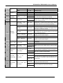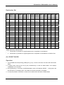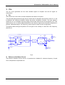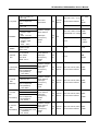
1
RPV599APIus/ RPU499APIus Service Manual Contents Preface……………………………………………………………………………………………2 Brief Introduction…………………………………….…………………………………………3 LCD………………………………………………………..………………………………………5 Radio Modes……………………………………………..………………………………………6 RPV599APlus Circuit Description………………………………………………….………37 RPU499APlus Circuit Description………………………………………………….………44 RPV599APlus Parts List ………………………………………….………………….………52 RPU499APlus Parts List………………………………………….……….………….………64 RPV599APlus Adjustment Description……………………..…………………….………82 RPU499APlus Adjustment Description…………………..……………………….………89 Pin function of CPU………………………………………………………….……….………94 Disassembly and Reassembly for Repair…………………….………………….………96 Description of main component………………………………..………………….………98 Exploded View…………………………………………………………………….….………101 Specifications……………………………………………..……………….…………………102 Packing……………………………………………..………………………………………103 RPV599AplusLevel Diagram………...…………..……………………………………104 Tx Section………………………………………………………………………………...105 RPU499AplusLevel Diagram…………………..……………………………………106 Tx Section…………………………………………………………………………...107 RPU-499 PC Board(Bottiom Layer)…….………..……………………………………108 RPU-499 PC Board(Top Layer)……….……….……………………………………109 RPU-499 Schematic Diagram……..…….…….………………………………….…110 RPU-499 Schematic Diagram(2)..……….…………………………………...…111 RPU-499 Schematic Diagram(3)..………....…………………………………...……112 RPU-499 Schematic Diagram(4)..……..….…………………………………...….113 RPV599 PC Board(Top Layer)…………..….………………………………………..114 RPV599 PC Board(Bottiom Layer)…..…….………………………………………115 RPV599 Schematic Diagram……..……..….………………………………….………116 1 RPV599APIus/ RPU499APIus Service Manual Preface Scope This manual is intended for use by qualified technicians familiar with similar types of communication equipment. It contains all service information and data required for the equipment. Caution The following precautions are recommended for personnel safety: y DO NOT transmit until all RF connectors are verified secure and all connectors are properly terminated. y SHUT OFF the power and DO NOT operate this equipment near electrical blasting caps or in a potential explosive atmosphere. y This equipment should be serviced by qualified technicians only. 2 RPV599APIus/ RPU499APIus Service Manual Brief Introduction 1 2 3 4 5 10 6 11 12 13 7 14 15 8 9 16 (1) ANTENNA (2) CHANNEL SELECTOR KNOB Used to select channel and squelch level. In addition, it can be programmed by the dealer to delete undesired channels from scan list or to select a CTCSS frequency. (3) (4) LED INDICATOR z Is red when transmitting z Is green when receiving z Flashes red when the battery voltage is low and approaching the cut-off point z Flashes orange, when the radio receives proper DTMF or Two Tone decode signals. ON-OFF/VOLUME KNOB Rotate the volume control knob clockwise to turn the unit “on” and fully counter clockwise to turn the unit “off”. Increase or decrease volume by adjusting the volume control accordingly. 3 RPV599APIus/ RPU499APIus Service Manual (5) SPEAKER (6) MICROPHONE (7) LCD Used to display channel and operation status. (8) (●,○,■,□) PROGRAMMABLE SOFT KEYS Used to enable auxiliary functions. Press each key to enable its corresponding function. (9) KEYPAD Used to enter, store or send DTMF codes. (10) PTT BUTTON Used to switch between transmit and receive mode. (11) LAMP BUTTON Used to turn on/off the LCD backlight. Press the [LAMP] button, the backlight will illuminate for about 5 seconds and then automatically turn off. Press any key other than [LAMP] button, the timer will retime. If you press the [LAMP] button, the backlight will light off. (12) MONI BUTTON Used to monitor the selected channels. (13) EXTERNAL SPEAKER-MICROPHONE JACK Used to connect with external speaker-microphone, programming cable, or cloning cable. (14) BELT CLIP (15) BATTERY (16) BATTERY LATCH 4 RPV599APIus/ RPU499APIus Service Manual LCD (1) Displays the selected channel number, channel frequency, channel label, squelch level or DTMF code. When selective call is enabled, messages received are also displayed here. Note: The “soft keys” can be programmed to toggle between display modes. Channel Number– Displays channel number. Factory default. Channel Frequency– Displays the channel frequency. Channel Label– Displays characters of the channel label (up to 16 alphanumeric characters can be programmed. Any label over 8 characters will scroll across the display). (2) Appears when Low Power is selected. (3) Appears when selected channel is busy. (4) Appears when MONI button is pressed to disable CTCSS, CDCSS, DTMF or 2-Tone. (5) Appears when MONI button is pressed to switch the speaker on. (6) Appears when current channel is in the scan list. Radio only scans channels in scan list. (7) Appears when enter number during channel label programming. Appears when CDCSS decoder is reversed in destination set mode. (8) Appears in scan mode. (9) Appears when keypad lock is on. 5 RPV599APIus/ RPU499APIus Service Manual Radio Modes 1. Frame of Radio Modes Select the function you want from the modes and make the necessary settings. USER MODE Conventional mode Self-Programming DEALER MODE Function Set Mode DTMF Set Mode New Function Set Mode Channel Set Mode Wired Clone Mode Wireless Clone Mode All Reset TEST MODE LCD Full Screen mode Destination Set Mode Frequency Display mode Alignment Mode PC MODE 6 RPV599APIus/ RPU499APIus Service Manual 2. Description of Mode Functions MODE USER MODE DEALER MODE USER SET MODE Self Programming (FUNCTION SET MODE) Self Programming (DTMF SET MODE) Self Programming (CHANNEL SET MODE) Self Programming (NEW FUNCTION MODE) WIRED CLONE MODE WIRELESS CLONE MODE ALL RESET TEST MODE MENU MODE ADJUSTMENT MODE FREQUENCY TEST MODE ADJUSTMENT DATA CLONE MODE LCD FULL SCREEN MODE DESTINATION SET MODE FUNCTION Conventional mode User Set Mode Dealer set the following modes: Function set mode, DTMF set mode, Channel set mode, Wired clone mode, Wireless clone mode, All Reset 1. Priority Channel 2. No.1 Home channel 3. No.2 Home channel 4. Programmable key 1 [●] 5. Programmable key 2 [○] 6. Programmable key 3 [■] 7. Programmable key 4 [□] 8. Power On Password The dealer set the following functions ON/OFF according to the user operating needs. 1.Monitor 2.Scan 3.Dial 4. Talk around 5.Low 6.Priority 7.Priority Channel 8.Look Back A 9.Look Back B 10.Revert Channel 11.TX Dwell time 12.Dropout Delay Time 13.Time out Timer 14.Tramsmit Warning 15.TOT Rekey Time 16.TOT Reset Time 17.Squelch Level 18.BEEP 19.Signalling 20.Battery Save 21.Selectable CTCSS 22.DELETE/ADD 23.Dealer Mode-Test Mode The dealer set the following functions ON/OFF according to the user operating needs. 24.Digit Time 25.Inter Digit Time 26.First Digit Time 27.Rise Time 28.Rise Time with CTCSS 29.PTT ID 30.Dial ID 31.Connect ID 32.Disconnect ID 33. NO. of DTMF key 34.DTMF Hold Time 35.Store & Send 36.D key Assignment 37.DTMF Signaling 38.Intermediate Code 39.Group Code 40 SQ. Auto Reset Time 41.Call Alert/ Transpond The dealers use this mode to set channel frequencies and signaling according to the user operating needs. 1.Channel Selection 2.RX Frequency 3.RX Signaling 4.TX Frequency 5.TX Signaling 6.DTMF/2-Tone signaling 7.PTT ID Enable 8.Scan DEL/ADD 9.Busy Channel Lockout 10.Clock Frequency Shift 11.TX Power 12.Wide/narrow Band 13. ID Code/RX 2-Tone 14. TX 2-Tone 15. Channel Label 45.Group Tone 46. Group Tone Duration 47. Channel Label Size 48. Programmable Key 1 [●] 49. Programmable Key 2 [○] 50. Programmable Key 3 [■] 51. Programmable Key 4 [□] 52. Power On Password 53. Data Password 54. Power On Text In this mode data is copied from one radio to another through a cable. In this mode data is copied from one radio to another without cable by means of the DTMF signal. In this mode transmit/receive frequencies of each channel and function settings are initialized. This mode is used to enter the following setting options. This mode is for alignment of radio operation. This mode is for checking the frequencies and repairing the radio. This mode is used to clone adjustment data from one radio to another. All characters and signs on the LCD are displayed. This mode sets radio destination. 7 RPV599APIus/ RPU499APIus Service Manual 3. Keypad Entry for Mode Startup MODE USER MODE Key Conventional Mode User Set Mode Function Set Mode DEALE R MODE TEST MODE Note: Remarks Turn on the power to enter Conventional Mode POWER ON While holding down [MONI] key, turn on the power While holding down [LAMP] and [ ] key simultaneously, turn on the power (in 2 seconds) ○ Press [ ●] key to enter Function Set Mode. DTMF Set Mode As above Press [ ○] key to enter DTMF Set Mode. Channel Set Mode As above Press [ ■] key to enter Channel Set Mode. New function set mode As above Press [ □] key to enter New Function Set Mode. Wired Clone Mode As above Press [LAMP] to enter Wired Clone Mode. Wireless Mode As above Press [MONI] to enter Wireless Clone Mode. All Reset As above Press [ Menu Mode While holding down [LAMP] and [ ] key simultaneously, turn on the power (in 2 seconds). Press [ Adjustment Mode Select “ADJUST” in menu mode. Clone Frequency Test Mode Adjustment Data Clone Mode LCD Full Screen Mode Destination Set Mode ■ Select “FREQ TST” in menu mode. Select “TUNE CLN” in menu mode. Select “FULL LCD” in menu mode. Select “DEST SET” in menu mode. □] key and [PTT] simultaneously. □] key to enter test mode and [■] key to return to Menu Mode. Press [ □] key to enter the mode and [■] key to exit. When power on password is enabled, you can enter the user mode only after inputting correct password. And if data password is enabled, you can enter the dealer mode and test mode only after inputting correct data password. You can input password through the keyboard and press [#] to clear. 8 RPV599APIus/ RPU499APIus Service Manual Prohibit entering dealer mode and test mode ◆ Dealer mode and test mode can be prohibited by programming to prevent users from changing the parameters with self-programming feature or with external programmer. ◆ Cancel the Prohibit Short the dealer mode control point and the test mode control point and then the prohibit will be cancelled at POWER-ON. Or use the programming software to cancel. Note: The dealer mode control point and the test mode control point locate over LCD and marked with SELF. DEALER MODE Self-Programming (Function Setting) 1. Turn on the power while pressing [LAMP] and [○] key, in 2 seconds the radio enters the dealer mode, and “SEL” appears on LCD. Note: If data password is enabled, you can enter the dealer mode and test mode only after inputting correct data password. In dealer mode, press [●] key to enter function set mode. 2. Use Channel Selector knob to set functions ON or OFF or to select the setting. 3. After a function is set, press [PTT] to store the setting and the menu goes to the next function option. 4. Press [●] key to return to Dealer Mode from current option, and the current data shown on the display will not be stored. 5. Press [PTT] to store current function setting and a beep will sound to confirm the action. 6. END appears when settings in function mode are completed. Function No. 1 2 Function Name MONITOR SCAN 3 [DIAL] 4 TALK AROUND Settings (Defaults are underlined) Display OFF MONI OFF Monitor Momentary MONI 1 Monitor Lock MONI 2 Remarks Invalid Signaling squelch is temporarily disabled while [MONI] button is held down. Signaling squelch is temporarily disabled while [MONI] button is pressed. Each time press can toggle between squelch disable and enable. SQ OFF Momentary OFF SCAN OFF Invalid CO SCAN CO “Carrier Operated” function TO Disable Enable SCAN TO DIAL OFF DIAL ON “Time Operated” function Disables the [DIAL] key. Enables the [DIAL] key. Disable TARE OFF Invalid Talk Around TARE TA “Talk around” function is enabled Reverse TARE RE “ Frequency Reverse” function is enabled MONI 3 9 Squelch is disabled while [MONI] button is held down. RPV599APIus/ RPU499APIus Service Manual 5 [LO] Disable LO ON Enables [LO] key. PRIO OFF PRIO FIX PRIO SEL PRICH 1 PRICH 99 NO priority setting Fixed priority channel Variable priority channel Priority channel (Only valid when “fixed priority” is enabled) The period time between radio back scanning a priority channel from a normal channel when there is no activity on priority channel The period time between radio back scanning a priority channel from a normal channel when there is activity on priority channel but not matching its signaling. Channel where scan starts. During scanning, it’s the latest channel at pause; during scan stopping, it’s the channel stopped; if scan never stops, it’s the start channel. During scanning, it’s the latest transmit channel; during scan stopping, it’s the channel stopped; if scan never stops, it’s the start channel. During scanning, it’s the start channel; during scan stopping, it’s the channel stopped. Priority channel 6 PRIORITY 7 PRIORITY CHANNEL 1 ~ 99 8 LOOK BACK 0.3s ~1.5s A (0.1s/1STEP) 10 11 1 0.5s LBA 300 LBA 1500 LOOK BACK 0.5s ~ 5.0s 2.0s (0.5s/1STEP) B REVERT LBB 500 Selected REV SEL Last Call REV LSTC Last Used REV LSTU Selected + Talk Back SEL TALK Priority REV PRIO Priority + Talk Back PRI TALK During scanning, it’s the priority channel; when scan stopping, it’s the channel stopped. 3.0s TSDT 0.5 Duration before scan restarts when it stops by transmission. 3.0s DODT 0.5 CHANNEL TX-SCAN 0.5s ~ 5.0s DWELL TIME (0.5s/1STEP) TSDT 5.0 12 DROP OUT DELAY TIME 0.5s ~ 5.0s (0.5s/1STEP) 13 TIME OUT TIMER OFF 30s~300s 60s (30s/1STEP) DODT 5.0 TOT OFF TOT 30 TOT 300 14 TOT PRE ALERT TIME OFF 1 ~ 60 (1s/1STEP) OFF 1s ~ 60s (1s/1STEP) OFF When OFF, in order to protect power amplifier, max. time of continuous transmission is set as 10 minutes. Maxi. time of continuous transmission TOT off. TOTA When this feature is enabled, the radio will call an alert at the set time. Transmission will be prohibited by TOT after this time. 1 TOTK OFF TOT REKEY TIME Duration before scan restarts when it stops by signal input. TOTA OFF TOTA 60 15 Disables [LO] key. Enable OFF Fixed Selected 9 LO OFF TOTK 1 TOTK 60 10 Duration until transmission is allowed after radio returning to receive mode by TOT. Transmit prohibited until preset time elapses. RPV599APIus/ RPU499APIus Service Manual 16 TOT RESET TIME OFF 1s ~15s OFF (1s/1STEP) TOTS OFF TOT is immediately reset after transmission stops. TOTS TOT won’t reset until preset time elapses, even if transmission has stopped. 1 TOTS 15 17 SQUELCH LEVEL 18 BEEP 19 SIGNALING 20 BATTERY SAVE 21 22 23 SELECTABLE CTCSS DELETE/ ADD ENABLE 0 ~9 5 (1s/1STEP) SQL 0 Squelch level is set higher (tighter), as the figure increases. SQL 9 NO BEEP OFF No beep tone YES BEEP ON Beep tone sounds AND SGNL AND Squelch is opened when both match. OR SGNL OR Squelch is opened when either matches. Disable BATT OFF No Battery Save function. Enable BATT ON Battery Save function. Disable Enable Disable VQT OFF VQT ON SADD OFF Prohibit Selectable CTCSS Permit Selectable CTCSS Prohibit Delete/Add Enable SADD ON Permit Delete/Add DEALER MODE/ TEST Disable MODE ENABLE Enable END MODE OFF Prohibit dealer mode and test mode MODE ON Permit dealer mode and test mode END When END is displayed, press [PTT] to return to Function Setting. Note: LOOK BACK: When radio is scanning a non-priority channel, the status of the priority channel will be detected periodically. The time interval for this detecting is as the following: A is period when there is no activity on the priority channel. B is period when there is activity on the priority channel, however not matching its signaling. Self-Programming (DTMF setting) 1. Turn on the power while pressing [LAMP] and [○] key simultaneously, and in 2 seconds the radio enters the dealer mode. In dealer mode, press [○] key to enter DTMF Set Mode. 2. Use Channel Selector knob and the 16 keys (0~9, *, #, A~D) to set DTMF function ON/OFF or select the setting. 3. Press [PTT] to store the selected settings, except functions 31 and 32, which are stored with the 16 keys, and the menu goes to next function option. 11 RPV599APIus/ RPU499APIus Service Manual 4. Press [○] key to return to Dealer Mode. The current setting displayed on LCD will not be stored. 5. Press [PTT] to store function settings and a Beep sounds to confirm the action. 6. END appears when all DTMF function settings are completed. 7. While pressing and holding [MONI], turn the channel selector to confirm the settings of each function option. Function No. Function Name Setting (Defaults are Display underlined) 24 DIGIT TIME 50ms ~ 200ms (10ms/1STEP) 50ms 25 INTER DIGIT TIME 50ms ~ 200ms (10ms/1STEP) 50ms 26 FIRST DIGIT TIME 50ms ~ 200ms (10ms/1STEP) 50ms DIGT 50 DIGT 200 IDT 50 IDT 200 FDT 50 FDT 200 RISE 100 Connect Disconnect Not send PTT ID. Press [PTT], PTT ID is sent. Release [PTT], PTT ID is sent. Both P.ID BOTH OFF D.ID OFF D.ID ON 100ms~1000ms 300ms (50ms/1STEP) 28 RISE TIME WITH CTCSS 100ms~1000ms 300ms (50ms/1STEP) OFF DIAL ID ON P.IDBEGIN 31 CONNECT ID Blank 0 × 1 ~ # × 16 -------0 FFFFFFFF P.ID END 32 DISCONNECT ID Blank 0 × 1 ~ # × 16 12keys 33 NO. of DTMF KEY 1st digit transmitting time during DTMF transmission. RTQT1000 P.ID OFF P.IDBEGIN P.ID END RISE TIME 30 Interval time between digits during DTMF transmission. RTQT 100 27 PTT ID One digit transmitting time during DTMF code transmission. Set the time between unmodulated carrier transmission and the DTMF code transmission Set time RISE1000 29 Remarks (0 ~ 9,*,#) -------0 Note: when DTMF function is enabled together with the Battery Save and CTCSS functions on, transmit delay time should be over 300 ms. Send PTT ID when both CONNECT and DISCONNECT. Prohibit Dial ID Permit Dial ID Display about one second when entering this setting. CONNECT ID is not set CONNECT ID is input (if more than 8, scroll it) Display about one second when entering this setting. Connect ID is not set. CONNECT ID is input (if more than 8, scroll it) FFFFFFFF DTMFK 12 Disable [A] [B] [C][D] keys. DTMFK 16 Enable [A] [B] [C][D] keys. 16keys (0 ~ 9,*,#,A ~ D) 12 RPV599APIus/ RPU499APIus Service Manual 34 STORE & SEND 36 D KEY ASSIGNMENT 37 DHT OFF Enable DHT ON OFF STSD OFF Function that continues transmission for two seconds even if manual Hold DIAL key is released. Prohibit Store & Send function. ON STSD ON Permit Store & Send function. D Code DKEYA D Send the code for D. 1s ~ 16s (1s/1STEP) DKEYA 1 DKEYA 16 Make unmodulated transmission for preset time. OFF DTMF OFF NO DTMF signaling. Code SQ DTMF CSQ Code Squelch SEL CALL DTMF SEL Selective Call DTMF HOLD TIME 35 DTMF SIGNALING 0~9 38 39 INTERMEDIATE CODE A~D GROUP CODE 41 42 End SQ AUTO RESET TIME CALL ALERT/ TRANSPOND 2 TONE SIDE TONE IMC 0 IMC 9 IMC A Selected code is set as intermediate code. IMC D * IMC E # IMC F OFF GRPC OFF A~D GRPC A GRPC D * GRPC E # GRPC F OFF 40 Do not Hold Disable 1s ~ 15s 10s (1s/1STEP) SART OFF SART 1 SART 15 OFF Call Alert (Ringing) CAT OFF CAT RING Call Alert (Beep) TRANSPOND (Call Alert) TRANSPOND (ID Code) CAT BEEP CAT CALT CAT IDCD TRANSPOND (Transpond Code) CAT TRCD OFF SIDET OFF ON SIDET ON No group code Selected code is set as group code. Do not perform Auto Reset. Auto Reset is performed for preset time. No operation The Call Alert (Ringing) tone sounds. The Call Alert (Beep) tone sounds. Responder of Call Alert. Responder of ID Code. Responder of code set in Auto Dial 0. No side tone sounds when transmitting 2-Tone. Side tone sounds simultaneously when transmitting 2-Tone. End When END appears, press [PTT], the radio returns to setting of "24. DIGIT TIME". 13 Time until coincidence state is canceled after DTMF/2-Tone signaling coincides. RPV599APIus/ RPU499APIus Service Manual Notes: When changing and storing the new setting of “DTMF SIGNALING” (function No. 37), the ID CODE setting in channel mode will be reset to “000”. And in self-programming set, the two-tone in all the channels will be reset to “1”. Notes in self-programming mode: In self-programming set, when the basic function is OFF, corresponding settings in the below table can be set, but not valid. Function name Settings Disable conditions 2-TONE/ DTMF DTMF 37.DTMF signaling is OFF 2.[SCN] TO 7.Priority is fixed or selected. 6.Priority Fixed, Selected 2.[SCN] is OFF 7.Priority CH 6.Priority is OFF or fixed. 8.Look Back A 6.Priority is OFF 9.Look Back B 6.Priority is OFF 10.Revert CH Priority, Priority + Selected 6.Priority is OFF 11.Dwell Time 2.[SCN] is OFF 12.Dropout Delay Time 2.[SCN] is OFF 14.TOT Pre-Alert 13.Time Out Time is OFF 15.TOT Rekey Time 13.Time Out Time is OFF 16.TOT Reset Time 13.Time Out Time is OFF 31.Connect ID 29.PTT ID is OFF or disconnected and 30. Dial ID is OFF 32.Disconnect ID 29.PTT ID is OFF or connected and 30. Dial ID is OFF. 38.Intermediate Code 37.DTMF/2-TONE signaling is OFF or is code SQ. 40.Unsquelch Time 37.DTMF/2-TONE signaling is OFF. 41.Call Alert/Transpond 37.DTMF/2-TONE signaling is OFF. Self- Programming (New Functions Setting) 1. Turn on the power while pressing [LAMP] and [○] key, the radio enters the DEALER MODE in 2 seconds. 2. 3. 4. 5. 6. In dealer mode, press [□] key, radio enters “new function set mode”. Rotate the channel selector knob to select the function setting. Press [PTT], the setting is stored and the menu goes to the next function option. Press [□] key again, display returns to “SEL” from current function setting, and the setting will not be stored. When setting function options, press [PTT], the settings will be stored and a BEEP sounds to confirm the operation. 14 RPV599APIus/ RPU499APIus Service Manual 7. End is displayed when all new functions settings are completed. Function Function Settings (Defaults are No. Name underlined) 45 NO GROUP TONE GRPT OFF 2-tone group tone off. Tone Type A TONE GRPT A Set 2-tone group tone as tone A. B TONE GRPT B Set 2-tone group tone as tone B. 0.5~10s 0.5s (step: 0.1s) GTDUR 0.5 Group tone time. OFF SIZE OFF SIZE 1 SIZE 16 Channel label display mode is disabled. 1~16 (step: 1) No Function K1 OFF SCAN K1 SCAN DIAL K1 DIAL TA K1 TARE LO K1 LO Display Label K1 DCHAR Display Frequency K1 DFREQ Display Mode K1 DMODE Scan ADD/DEL K1 SADD Key Lock K1 KLOCK Variable QT K1 VQT SQL Nuisance Channel Delete K1 SQL K1 NUISA Temporarily remove a "nuisance" channel. Priority Channel Delete K1 PDEL Temporarily remove the priority channel. Home Channel K1 HOME No Function K2 OFF SCAN K2 SCAN DIAL K2 DIAL TA K2 TARE LO K2 LO Display Label K2 DCHAR Display Frequency K2 DFREQ Display Mode K2 DMODE Scan ADD/DEL K2 SADD Key Lock K2 KLOCK Variable QT K2 VQT SQL K2 SQL Nuisance Channel Delete K2 NUISA Temporarily remove a "nuisance" channel. Priority Channel Delete K2 PDEL Temporarily remove the priority channel. Home Channel K2 HOME 46 47 Channel Label Size 49 Remarks Group Group Tone Duration 48 Display KEY1 KEY2 15 <- Default <- Default RPV599APIus/ RPU499APIus Service Manual 50 KEY3 No Function K3 OFF SCAN K3 SCAN DIAL K3 DIAL TA K3 TARE LO K3 LO Display Label K3 DCHAR Display Frequency K3 DFREQ Display Mode K3 DMODE Scan ADD/DEL K3 SADD Key Lock K3 KLOCK Variable QT K3 VQT SQL K3 SQL Nuisance Delete 51 KEY4 52 Power On Password 53 Data Password 54 Power On Text Channel <- Default K3 NUISA Temporarily remove a "nuisance" channel. Priority Channel Delete K3 PDEL Temporarily remove the priority channel. Home Channel K3 HOME No Function K4 OFF SCAN K4 SCAN DIAL K4 DIAL TA K4 TARE LO K4 LO Display Label K4 DCHAR Display Frequency K4 DFREQ Display Mode K4 DMODE Scan ADD/DEL K4 SADD Key Lock K4 KLOCK Variable QT SQL Nuisance Channel Delete Priority Channel Delete Home Channel K4 VQT K4 SQL <- Default K4 NUISA Temporarily remove a "nuisance" channel. Temporarily remove the priority channel. -------20040101 K4 PDEL K4 HOME POWERKE Y -------20040101 Data Password DATA KEY -------20040404 -------20040404 Power On Text POWERTXT -------- -------- 123ABC@# 123ABC@# Power On Password 16 Display about one second when entering this setting. No password is input Max. 8 digit (0-9) Display about one second when entering this setting. No password is input Max. 8 digit (0-9) Display about one second when entering this setting. No text is input Maximum 8 characters (0-9,A-Z, symbols) (Refer to appendix 1: channel label programming) RPV599APIus/ RPU499APIus Service Manual Self-programming (channel setting) 1. Turn on the power while pressing [LAMP] and [○] key, radio enters the dealer mode in 2 seconds. 2. In dealer mode, press [■] key, radio enters Channel Set Mode. 3. Using Channel Selector knob and 16 keys (0~9, *, #, A~D) to select channel functions or settings. 4. Press [PTT], the settings are stored and the menu moves to the next function set. 5. Press [■] key, radio returns to Dealer Mode from current function set. And current setting displayed on LCD will not be stored. 6. During functions setting, pressing [PTT] can store selected settings, which will be confirmed by a Beep. 7. END is displayed when all Channel settings are completed. Function Settings (Defaults are Name underlined) Channel Select Display Remarks CH 1 ◆ CH 99 setting. Blank ------------ ◆ 100.000MHz or more 100.00000 1CH ~ 99CH 1CH Under 550MHz (2.5KHz steps) RX “RX FREQUENCY” frequency change→Channel Selector knob Toggle between 6.25/2.5KHz steps→ [ ◆ 549.99750 ◆ 100.00000 ◆ Toggle between blank/frequency→[ □] key Change to 1MHz steps→[LAMP] + Channel Selector knob Under 550.000.MHz (6.25KHz steps) ●] key (Dot means 6.25KHz) FREQUENCY 100.000MHz or more setting follows this 549.99375 ◆ The initial value when changing from blank to frequency display is the initial value of the OFF CTCSS (standard) 67.0Hz ~ 250.3Hz CTCSS (not standard) (0.1Hz step) OFF QT 67.0 QT 250.3 QT 67.0* QT 250.3* ◆ Code selection → Channel Selector knob ◆ CTCSS changes in 0.1 Hz step increment → [●] key RX CTCSS 67.0Hz ~ 250.3 Hz SIGNALING CDCSS (standard) DQT023N DQT754I ◆ CDCSS changes in 1 step increment,→ [ ] key ◆ Toggle signaling between CDCSS and CDCSS (not standard) (step:1) 000.~777. (octonary) DQT000N* –CDCSS→[ ● ◆ DQT777I* 17 ○]. Toggle among blank, CTCSS frequency and CDCSS→[ □] key RPV599APIus/ RPU499APIus Service Manual Blank TX FREQUENCY ------------- 100.000MHz or more 100.00000 Under 550MHz 549.99750 (2.5KHz steps) 100.000MHz or more 100.00000 Under 550.000MHz 549.99375 (6.25KHz steps) OFF frequency change → Channel Selector knob Toggle between 6.25/2.5KHz step increment → [ ] key ◆ Toggle between Blank/ CTCSS display→[ ] key ◆Change to 1MHz step increment → [LAMP]+Channel Selector knob ◆ The initial value from blank to frequency display is the value set in RX FREQUENCY ◆ If blank is set, menu enters to the option of “DTMF SIGNALING”. ◆select codes → Channel Selector knob ◆ OFF ● ◆ □ CTCSS (standard) QT 67.0 67.0 HZ ~ 250.3Hz QT 250.3 CTCSS (not standard) QT 67.0* ◆ TX CTCSS (0.1Hz step mode) QT 250.3* ◆ SIGNALING 67.0Hz ~ 250.3Hz CDCSS (standard) CTCSS changes in 0.1Hz step increment →[ ◆ 000.~777. (octonary) DTMF/2-TONE SIGNALING ANI DQT023N [□] key. DQT000N* “DTMF SIGNALING/2-Tone” settings follow this setting ◆ DQT777I* No DTMF Signaling/2 Tones DTMF SIG DTMF Use DTMF Signaling 2 Tones SIG TTS Use 2 Tones OFF ANI OFF Disable ANI ON ANI ON Enable ANI ADD SCAN ADD Set in scan list DELETE SCAN DEL Delete from scan list OFF B.C.L.O Busy channel lock out is disabled LOCKOUT 1 B.C.L.O 1 Transmission is prohibited if a signal appears with incompatible CTCSS/CDCSS; LOCKOUT 2 B.C.L.O 2 Transmission is prohibited if a signal appears with incompatible CTCSS/CDCSS or DTMF/2-Tone. Disable SHFT OFF Do not shift clock frequency Enable SHFT ON Shift clock frequency High TXPWR H Permit switching between High/Low Power Low TXPWR L Permit only Low Power LOCK OUT CLOCK SHIFT ○ SIG OFF OFF SCAN DELETE/ADD BUSY CHANNEL ●] key. Toggle signaling between CDCSS and –CDCSS→[ ] key. ◆Toggle among blank, CTCSS frequency and CDCSS→ DQT754I CDCSS (not standard) (step:1) CDCSS changes in 1 step increment→[ ●] key. TX POWER 18 [ANI] function setting follows this setting. RPV599APIus/ RPU499APIus Service Manual Wideband/Narrowband ID CODE (DTMF) 2-Tone signaling Wide Narrow WIDE NARROW ID 000 9999999999 -------0 Display about one seconds when entering this setting. ID is input, enter number→[10 digit keys(0-9)] 9999999999 If more than 8, scroll it RX 2-TONE 1-16 1 TX 2-TONE 1-16 1 TTS_R 1 ◆Code selection→Channel selector knob ◆ Return to “Channel Select” function when 99 channels are not all set. ◆When 99 channels are all set, END is displayed. Display about one seconds when entering this setting. No channel label is input Maximum 16 characters (0-9,A-Z, symbols) (Refer to appendix 1: channel label programming) TTS_T 1 -------Label (1 to 16 alphanumeric characters can be used) Channel Label END CH LABEL ------123ABC@# Wide mode Narrow mode Only appears in 99th channel END Note: 1. If DTMF or DTMF/2-Tone is disabled, “ID code” function option is automatically skipped. 2. DTMF and 2-Tone cannot be enabled simultaneously. Appendix 1: Channel Label Programming CHARACTER INPUT KEY INPUT Number of times key is pressed 1 1 NUMBER 2 3 4 5 6 Space 1 2 A B C 2 3 D E F 3 4 G H I 4 5 J K L 5 6 M N O 6 7 P Q R 8 T U V 9 W X Y 0 A~Z A @ # $ % ^ * A B , . ‘ “ ? : B C + - \ / = _ C D < > ( ) [ ] D * /T9 # PTT Channel selector knob S 7 8 Z 9 0 Press to toggle between Character and Number. “V” on LCD indicates number input. → REMARKS (Next alphanumeric) Enter (Complete programming and store channel label) ←, → (Move cursor backward/forward) 19 Cursor: current input position will toggle between char/num and cursor display. Each key can generate numeric and character information. Pressing a key will cause the first character of the key’s character cycle to appear on the LCD; Subsequent pressing of the same key will cause subsequent characters in the cycle to appear. For example, to enter the character “S”, press the “7” key four (4) times. RPV599APIus/ RPU499APIus Service Manual Appendix 2: CTCSS Frequency No. Frequency [Hz] No. Frequency [Hz] No. Frequency [Hz] No. Frequency [Hz] 1 67.0 11 94.8 21 131.8 31 186.2 2 69.3 12 97.4 22 136.5 32 192.8 3 71.9 13 100.0 23 141.3 33 203.5 4 74.4 14 103.5 24 146.2 34 210.7 5 77.0 15 107.2 25 151.4 35 218.1 6 79.7 16 110.9 26 156.7 36 225.7 7 82.5 17 114.8 27 162.2 37 233.6 8 85.4 18 118.8 28 167.9 38 241.8 9 88.5 19 123.0 29 173.8 39 250.3 10 91.5 20 127.3 30 179.9 Appendix 3: 2-Tone frequency (Default) No. Tone A Freq [Hz] Tone B Freq [Hz] Tone A Dur. (s) Tone B Dur. (s) Gap Time (s) 1 400 1141 0.5 0.5 0.5 2 456 1301 0.5 0.5 0.5 3 520 1483 0.5 0.5 0.5 4 593 1690 0.5 0.5 0.5 5 675 1927 0.5 0.5 0.5 6 770 2197 0.5 0.5 0.5 7 878 2504 0.5 0.5 0.5 8 1001 2855 0.5 0.5 0.5 9 1141 400 0.5 0.5 0.5 10 1301 456 0.5 0.5 0.5 11 1483 520 0.5 0.5 0.5 12 1690 593 0.5 0.5 0.5 13 1927 675 0.5 0.5 0.5 14 2197 770 0.5 0.5 0.5 15 2504 878 0.5 0.5 0.5 16 2855 1001 0.5 0.5 0.5 20 RPV599APIus/ RPU499APIus Service Manual Wired Clone Mode Connect the source radio and the target radio with an interface cable. Source radio Operation 1. Turn POWER ON while holding down [LAMP] and [○] key, in about 2 seconds the radio enters the Dealer Mode. Then press [LAMP] to enter Clone Mode. [LAMP] 2. Transmit the clone data by pressing [MONI], red LED glows during data transfer. When data transfer is completed, “END” is displayed on LCD, and the red LED turns off. 3. When “End” is displayed, press [MONI] button to continue to clone another radio or press [LAMP] to return to Dealer Mode. [MONI] Sending clone data Red LED on clone data transfer end Red LED off [LAMP] Dealer Mode Target radio Operation 1. Turn On the power. When data is being sent from the master, busy mark and "-PC-" appears on LCD. Dealer Mode Clone Mode 21 RPV599APIus/ RPU499APIus Service Manual 2. When all data is received, “END” displays on LCD. After the “END” appears, operation is same as the source radio operation 3. Note: During cloning, do not execute any action that might interrupt the cloning such as shutting off power. Wireless Clone Mode Setup the source side and target side. Source Side Operation 1. Turn POWER ON while holding down [LAMP] and [○] key, in about 2 seconds radio enters the Dealer Mode. Then press [MONI], radio enters Wireless Clone Mode, now the frequency displayed on LCD is the initial frequency matching the destination. [ MONI ] Dealer Mode Clone Mode 2. Turn Channel Selector knob to select the frequency used for the wireless clone. [Channel Selector] Dealer Mode Clone Mode 3. Start the first half (00-50%) data transmission by pressing [PTT]. “00 CLONE” is displayed on LCD and red LED glows. The leftmost digits (00) on LCD show data transfer rate, and as data transmission proceeds, the digits count upwards in increments of 1. Transmit power is set as LOW POWER. [PTT] Clone Mode Clone Mode 22 Red LED lights up RPV599APIus/ RPU499APIus Service Manual 4. When the first half data transfer is completed, the LED turns off and “END” is displayed. Press [MONI], radio returns to Clone Mode and you can clone another half by pressing [LAMP] or return to Dealer Mode by pressing [MONI] key. Clone Mode 5. Clone Mode You can continue to clone another half (50-100%) data mainly about channel label after one minute to avoid long time transmission. 6. Start another half (50-100%) data transmission by pressing [LAMP]. “50 CLONE” is displayed on LCD and red LED glows. The leftmost digits (50) on LCD show data transfer rate, and as data transmission proceeds, the digits count upwards in increments of 1. Transmit power is set as LOW POWER. [LAMP] Clone Mode 7. Clone Mode Red LED lights up When the second half data transfer is completed, the LED turns off and “END” is displayed. Press [MONI], radio returns to Clone Mode and you can clone another radio or press [MONI] to return to Dealer Mode. Clone Mode Clone Mode Target Side Operation 1. Turn POWER ON while pressing [LAMP] and [○] key, in about 2 seconds radio enters the Dealer Mode. Then press [MONI] to enter Wireless Clone Mode. The frequency displayed on LCD is the initial frequency matching the destination. 2. The display changes to “00 CLONE” or “50 CLONE” correspondingly when the radio receives data from the master and the BUSY mark appears. The leftmost digits (00) or (50) on the LCD show the data transfer rate and as data reception proceeds, the digits count upwards in increments of 1. [Receive DTMF Data] Clone Mode [Receive DTMF Data] Clone Mode Clone Mode 23 Clone Mode RPV599APIus/ RPU499APIus Service Manual 3. When all data is received, “END” displays. The display of first half and second half transfer is shown as following respectively. [Data receive complete] Clone Mode Clone Mode [Data receive complete] Clone Mode Clone Mode 4. When “END” displays, the next operation is same as the source side operation 4. Please confirm the following operations: (1) Attach the antenna to the source radio. (2) Remove the antenna from the target radio. (3) Keep radios as close as possible. Note: During cloning do not execute any action that might interrupt the cloning such as shutting off power. TEST MODE Menu Mode 1. Turn the power ON while pressing [LAMP] and [■] key, in about 2 seconds the radio enters Test Mode and LCD displays “TEST”. After two seconds, the first setting option “ADJUST” is displayed on LCD. Turn Channel Selector knob to select from the following menu: ADJUST FREQ TST TUNE CLN FULL LCD DEST SET 2. Press [□] key to enter Adjustment Mode, Frequency Test Mode, Adjustment Data Clone Mode, LCD Full Screen Mode or Destination Set Mode. 3. Press [■] key to return to the Menu Mode. 24 RPV599APIus/ RPU499APIus Service Manual LCD Full Screen Mode 1. Turn the power ON while pressing [LAMP] and [■] key simultaneously, in about 2 seconds the radio enters the menu of Test Mode. 2. Turn Channel Selector knob to select the setting option: “FULL LCD”. 3. Now press [□] key to enter LCD Full Screen Mode. 4. Press [■] key to exit from LCD Full Screen Mode. LCD displays “FULL LCD”. [□] [■] Test Mode LCD Full Screen Mode Adjustment Data Clone Mode 1. Turn the power ON while pressing [LAMP] and [■] key, in about 2 seconds the radio enters the menu of Test Mode. 2. Turn Channel Selector knob to select the setting option “TUNE CLN”. 3. Connect the source radio and the target radio with an interface cable. 4. Turn the target radio on. 5. Now press [□] key to enter Adjustment Data Clone Mode. LCD displays “–C–“. 6. Press [MONI] key to transmit the adjustment data. 7. Red LED glows during data transfer. When data transfer is completed, “END” is displayed on LCD and red LED turns off. 8. When “End” is displayed, press [MONI] to continue to clone another radio. 9. Press [■] key to exit from Adjustment Data Clone Mode. LCD displays “TUNE CLN”. Destination Set Mode Operation 1. Turn the power ON while pressing [LAMP] and [■] key, in about 2 seconds the radio enters the menu of Test Mode. 2. Turn Channel Selector knob to select the setting option “DEST SET”. 25 RPV599APIus/ RPU499APIus Service Manual 3. Now press [□] key to enter Destination Set Mode, LCD displays “ MODEL X“. (X=0~15) 4. Turn Channel Selector knob to change the destination number. (Display numbers change from 0 to 15). 5. Hold down [MONI] key and then press [□] key to select the display number that you need as the destination. 6. Press [LAMP] key to reverse CDCSS decoder and LCD displays “V”. (For factory setting only). 7. Press [■] key to exit from Destination Set Mode. LCD displays “DEST SET”. [□] Test Mode Destination Set Mode [Channel Selector] [■] Destination Set Mode [PTT] [MONI]+[□] Destination on dispiay is stored in the memory Note: 1. Once the destination is set, previous channel settings (frequencies, CTCSS and channel functions) will be deleted and some functions are also changed. Therefore, do not make destination set except when EEPROM is replaced or other unavoidable conditions happened. 2. Destination of RPV599APlus is set as 8, frequency is 148~174MHz. And destination of RPU499APlus is 11, frequency 450-470MHz. Frequency Test Mode (for frequencies checking and radios repairing) Operation 1. Turn POWER ON while pressing [LAMP] and [■] key, in about 2 seconds the radio enters the menu of Test Mode. 2. Turn Channel Selector knob to select the setting option “FREQ TST”. 26 RPV599APIus/ RPU499APIus Service Manual 3. Press [□] key to enter Frequency Display Mode. LCD displays frequency. 4. Turn Channel Selector knob to increase/decrease the frequency. 5. Press [○] key to switch the step increments. 6. Press [□] key to toggle between High and Low Power. 7. Press [●] key, the radio enters scan mode. 8. Press [PTT] to transmit and [MONI] to monitor. 9. Hold down [LAMP] and then press [○] key, the radio enters CTCSS set mode. 10. Press [■] key to exit from Frequency Display Mode, LCD displays “FREQ TST”. [□] [■] Test Mode Frequency Display Mode Notes: 1. The reset (initial) frequency varies according to the destination. 2. Set initial transmit power to LO POWER. Changing the Frequency Operation 1. In Frequency Test Mode, turn Channel Selector knob clockwise, the frequency increases in step increments. Turn the knob counterclockwise, the frequency decreases in step increments. 2. Hold down the [LAMP] key, and then turn the Channel Selector knob to change the frequency in 1MHz step increments. 3. Press [○] key, the step increment is switched in the following order. 2.5KHz 6.25KHz 5KHz 12.5KHz Notes: 1. The frequency display range is between 100MHz and 550MHz. When PLL is unlocked, “beeps” sound. The frequency should not be out of corresponding frequency spectrum. 2. Step increment is not displayed on LCD. 27 RPV599APIus/ RPU499APIus Service Manual CTCSS Operation 1. In Frequency Test Mode, hold down [LAMP] and then press [○] key, the radio enters CTCSS set mode. Turn Channel Selector knob to change the CTCSS frequency. 2. Press any key to select the CTCSS you need and the radio returns to frequency display mode. [LAMP]+[DIAL] [LAMP]+[ ○] [Channel Selector] [KEY] Notes: 1. The selected CTCSS is set for both transmit and receive. 2. The selected CTCSS frequency cannot be changed in 0.1Hz step increments. 3. During test scan, even if [○] key and [LAMP] are simultaneously held down, the radio will not enter CTCSS set mode. Adjustment Mode (Adjustment procedure used during radio repairing) Menu Mode 1. Turn POWER ON while pressing [LAMP] and [■] key, in about 2 seconds, the radio enters the menu of Test Mode. LCD displays “TEST” for 2 seconds and then begins to display “ADJUST”. 2. Turn Channel Selector knob to select the setting option “ADJUST”. 3. Now press [□] key to enter Adjustment Mode, the first option “HI POWER” is displayed on LCD. 28 RPV599APIus/ RPU499APIus Service Manual 4. Turn Channel Selector knob to select a setting option from the following menu: HI POWER LO POWER BATT REF CTCSS W CDCSS W CTCSS N CDCSS N SQL CEN SQL LOW SQL HIGH 5. Press [□] key to adjust the Transmit High Power, Transmit Low Power, Battery Reference Value, CTCSS Deviation (Wideband), CDCSS Deviation (Wideband), CTCSS Deviation (Narrowband), CDCSS Deviation (Narrowband), BUSY Reference Value (Center Frequency), BUSY Reference Value (Low Frequency) and BUSY Reference Value (High Frequency) individually. 6. Press [■] key to exit from the Adjustment Mode and return to the menu of Test Mode. LCD displays “ADJUST”. Adjusting Transmit High Power Use this procedure to adjust the transmit High Power level. 1. Connect the power meter to the radio. 2. Turn Channel Selector knob to select the setting option “HI POWER”. 3. Transmission is performed automatically at High Power when the [□] key is pressed. After the frequency is displayed for one second, the display “HPWR XXX” now appears. (XXX=0 to 255) 4. Turn the channel selector knob while observing the power meter to obtain the transmit power needed. Turn the channel selector knob clockwise for an increase in power, and counterclockwise for a decrease in power. 5. Press [□] key to store the alignment value into the memory and return to the “LO POWER” display. Press [■] key to cancel the alignment value and return to the “HI POWER” display. 29 RPV599APIus/ RPU499APIus Service Manual Adjusting Transmit Low Power Use this procedure to adjust the transmit Low Power level. 1. Connect the power meter to the radio. 2. Turn Channel Selector knob to select the setting option “LO POWER”. 3. Transmission is performed automatically at Low Power when the [□] key is pressed. After the frequency is displayed for one second, the display “LPWR XXX” now appears. (XXX=0 to 255) 4. Turn the channel selector knob while observing the power meter to obtain the transmit power needed. Turn the channel selector knob clockwise for an increase in power, and counterclockwise for a decrease in power. 5. Press [□] key to store the alignment value into the memory and return to the “BATT REF” display. Press [■] key to cancel the alignment value and return to the “LO POWER” display. Adjusting the Battery Reference Value Use this procedure to adjust the reference value for issuing battery low voltage alarms. 1. Using an external power supply feed in the reference value at which you wish to trigger the alarm. 2. Turn Channel Selector knob to select the setting option “BATT REF”. 3. Transmission is performed automatically at High Power when the [□] key is pressed. After the frequency is displayed for one second, the display “BATT XXX” now appears. (XXX=1 to 255). 4. Adjust by turning the Channel Selector knob counterclockwise so that the red LED lights up and turning clockwise so that the red LED flashes. The point where the red LED is flashing indicates detection of the low voltage. 5. Press [□] key to store the alignment value into the memory and return to the “CTCSS W” display. Press [■] key to cancel the alignment value and return to the “BATT REF” display. 30 RPV599APIus/ RPU499APIus Service Manual Adjusting CTCSS Deviation (Wideband) Use this procedure to adjust the transmit CTCSS deviation (Wideband). 1. Connect the modulation analyzer to the radio. 2. Turn Channel Selector knob to select the setting option “CTCSS W”. 3. Transmission is performed automatically at Low Power and the preset CTCSS is sent when the [□] key is pressed. After the frequency is displayed for one second, the display “CTCW XXX” now appears (XXX=1 to 255). If the CTCSS is set OFF, then 67.0Hz is sent. 4. Hold down [LAMP] button to observe CTCSS and adjust CTCSS by turning Channel Selector knob. 5. While observing the modulation analyzer, adjust the deviation with the Channel Selector knob. 6. Press [□] key to store the alignment value into the memory and return to the “CDCSS W” display. Press [MONI] to cancel the alignment value and return to the “CTCSS W” display. Adjusting CDCSS Deviation (Wideband) Use this procedure to adjust the transmit CDCSS deviation (Wideband). 1. Connect the modulation analyzer to the radio. 2. Turn Channel Selector knob to select the setting option “CDCSS W”. 3. Transmission is performed automatically at Low Power and the preset CDCSS is sent when the [□] key is pressed. After the frequency is displayed for one second, the display “CDCW XXX” now appears (XXX=1 to 255). If the CDCSS is set OFF, then 023 is sent. 4. While observing the modulation analyzer, adjust the deviation with the [CHANNEL SELECTOR]. 5. Press [□] key to store the alignment value into the memory and return to the “CTCSS N” display. Press [■] key to cancel the alignment value and return to the “CDCSS W” display. 31 RPV599APIus/ RPU499APIus Service Manual Adjusting CTCSS Deviation (Narrowband) Use this procedure to adjust the transmit CTCSS deviation (Narrowband). 1. Connect the modulation analyzer to the radio. 2. Turn Channel Selector knob to select the setting option “CTCSS N”. 3. Transmission is performed automatically at Low Power and the preset CTCSS is sent when the [□] key is pressed. After the frequency is displayed for one second, the display “CTCN XXX” now appears (XXX=1 to 255). If the CTCSS is set OFF, then 67.0Hz is sent. 4. Hold down [LAMP] button to observe CTCSS and adjust CTCSS by turning Channel Selector knob. 5. While observing the modulation analyzer, adjust the deviation with the Channel Selector knob. 6. Press [□] key to store the alignment value into the memory and return to the “CDCSS N” display. Press [■] key to cancel the alignment value and return to the “CTCSS N” display. Adjusting CDCSS Deviation (Narrowband) Use this procedure to adjust the transmit CDCSS deviation (Narrowband). 1. Connect the modulation analyzer to the radio. 2. Turn Channel Selector knob to select the setting option “CDCSS N”. 3. Transmission is performed automatically at Low Power and the preset CDCSS is sent when the [PTT] key is pressed. After the frequency display for one second, the display “CDCN XXX” now appears (XXX=1 to 255). If the CDCSS is set OFF, then 023 is sent. 4. While observing the modulation analyzer, adjust the deviation with the Channel Selector knob. 5. Press [□] key to store the alignment value into the memory and return to the “SQL CEN” display. Press [■] key to cancel the alignment value and return to the “CDCSS N” display. Adjusting the BUSY Reference Value (Center Frequency) Use this procedure to align squelch level 3 and 9 at center frequency. 1. Connect the signal generator to the radio. 2. Turn Channel Selector knob to select the setting option “SQL CEN”. 3. Input a signal at the level at which you want squelch 9 to open. 32 RPV599APIus/ RPU499APIus Service Manual 4. Press [□] key to receive this signal. After the center frequency is displayed for one second, the display “SQL9 XXX” now appears. (XXX =1 to 255) 5. Turn Channel Selector knob to the position where you want the squelch to open. Rotate Channel Selector knob clockwise, the squelch is tightened. 6. Press and hold [LAMP] button to observe the center frequency and adjust the frequency by Channel Selector knob. 7. Press [■] key to cancel the setting and return to the “SQL CEN” display. Press [□] key to save the alignment value into the memory and continue to the alignment of squelch 3, and now “SQL3 XXX” displays. (XXX=1 to 255) 8. Then output a signal from the signal generator at which you want squelch 3 to open. Adjust by using the Channel Selector knob just same as with squelch 9. 9. Press [□] key to store the alignment value into the memory and return to the “SQL LOW” display. Press [■] key to cancel the alignment value and return to the “SQL CEN” display. Adjusting the BUSY Reference Value (Low Frequency) Use this procedure to align squelch level 3 and 9 at low frequency. 1. Connect the signal generator to the radio. 2. Turn Channel Selector knob to select the setting option “SQL LOW”. 3. Input a signal at the level at which you want squelch 9 to open. 4. Press [□] key to receive this signal. After the low frequency is displayed for one second, the display “SQL9 XXX” now appears. (XXX =1 to 255) 5. Turn Channel Selector knob to the position where you want the squelch to open. Rotate Channel Selector knob clockwise, the squelch is tightened. 6. Press and hold [LAMP] button to observe the low frequency and adjust the frequency by Channel Selector knob. 33 RPV599APIus/ RPU499APIus Service Manual 7. Press [■] key to cancel the setting and return to the “SQL LOW” display. Press [□] key to save the alignment value into the memory and continue to the alignment of squelch 3, and now “SQL3 XXX” displays. (XXX=1 to 255) 8. Then output a signal from the signal generator at which you want squelch 3 to open. Adjust by using the Channel Selector knob just same as with squelch 9. 9. Press [□] key to store the alignment value into the memory and return to the “SQL HIGH” display. Press [■] key to cancel the alignment value and return to the “SQL LOW” display. Adjusting the BUSY Reference Value (High Frequency) Use this procedure to align squelch level 3 and 9 at high frequency. 1. Connect the signal generator to the radio. 2. Turn Channel Selector knob to select the setting option “SQL HIGH”. 3. Input a signal at the level at which you want squelch 9 to open. 4. Press [□] key to receive this signal. After the high frequency is displayed for one second, the display “SQL9 XXX” now appears. (XXX =1 to 255) 5. Turn Channel Selector knob to the position where you want the squelch to open. Rotate Channel Selector knob clockwise, the squelch is tightened. 6. Press and hold [LAMP] button to observe the high frequency and adjust the frequency by Channel Selector knob. 7. Press [■] key to cancel the setting and return to the “SQL HIGH” display. Press [□] key to save the alignment value into the memory and continue to the alignment of squelch 3, and now “SQL3 XXX” displays. (XXX=1 to 255) 8. Then output a signal from the signal generator at which you want squelch 3 to open. Adjust by using the Channel Selector knob just same as with squelch 9. 9. Press [□] key to store the alignment value into the memory and return to the “HI POWER” display. Press [■] key to cancel the alignment value and return to the “SQL HIGH” display. 34 RPV599APIus/ RPU499APIus Service Manual Destination Set model Default DTMF Frequency CTCSS CDCSS 2-Tone Busy Busy /CDCSS TX/RX Channel Channel with Lockout 1 Lockout 2 (MHz) First Busy Center Low High IF(MHz) Channel (MHz) (MHz) (MHz) Lockout Same Phase CTCSS/ DTMF/ CDCSS 2-Tone 0 143 √ √ √ √ √ √ 45.05 *1、*2 143 136 150 1 160 √ √ √ √ √ √ 45.05 1、2 160 148 174 2 410 √ √ √ √ √ 46.35 1、2 410 400 420 3 455 √ √ √ √ √ 45.05 1、2 455 440 470 4 460 √ √ √ √ √ 45.05 1、2 460 450 470 5 480 √ √ √ √ √ 45.05 1、2 480 470 490 6 490 √ √ √ √ √ 46.35 1、2 490 480 500 7 140 √ √ √ √ √ √ 45.05 1、2 140 136 150 8 160 √ √ √ √ √ √ 45.05 1、2 160 148 174 9 410 √ √ √ √ √ 46.35 1、2 410 400 420 10 455 √ √ √ √ √ 45.05 1、2 455 440 470 11 460 √ √ √ √ √ 45.05 1、2 460 450 470 12 480 √ √ √ √ √ 45.05 1、2 480 470 490 13 490 √ √ √ √ √ 46.35 1、2 490 480 500 14 360 √ √ √ √ √ 46.35 1、2 360 350 370 15 380 √ √ √ √ √ 45.05 1、2 380 370 390 Note: About busy channel lockout * * 1: Transmission is prohibited if a signal appears with incompatible CTCSS/CDCSS; 2: Transmission is prohibited if a signal appears with incompatible CTCSS/CDCSS or DTMF/2-Tone. ALL RESET MODE Operation 1. Turn POWER ON while pressing [LAMP] and [○] key, in about 2 seconds, the radio enters the Dealer Mode. 2. In dealer mode, press [PTT] and [□] key simultaneously to enter All Reset Mode. LCD displays “LMPRESET” for 5 seconds. 3. Press [LAMP] key in 5 seconds, the EEPROM data is reset. LCD displays “RESET…” during reset, and red LED glows. LCD displays “SEL” and LED turns off when All Reset is completed. 4. If no key is pressed in 5 seconds, no reset occurs and the radio will return to Dealer Mode. 35 RPV599APIus/ RPU499APIus Service Manual PC MODE Connection procedures 1. Connect the radio of RPV599APlus/RPU499APlus to the personal computer with an interface cable. 2. Run the program on the computer and Turn ON the power of the radio. 3. You can read, programme or adjust the radio via RPV599APlus/RPU499APlus programming software. Please refer to “RPV599APlus/RPU499APlus Editing Software User Manual” for details. 36 RPV599APIus/ RPU499APIus Service Manual RPV599APlus Circuit Description 1. FREQUENCY CONFIGURATION The receiver utilizes double conversion. The first IF is 45.05 MHz and the second IF is 455KHz. The first local oscillator signal comes from the PLL circuit. The PLL circuit in the transmitter generates the necessary frequencies (See Fig.1). CF 455KHZ ANT MCF ANT SW PA AMP RF AMP IF SYSTEM AF AMP SP TX AMP PLL VCO MIC AMP MIC 12.8MHz Fig.1 2. RECEIVER SYSTEM The frequency configuration of the receiver is shown as following fig.2 ANT CF1,2 BPF L32 RF AMP Q39 BPF L24,L26 MIXER Q29 ANT SW MCF XF1 IF AMP Q21 AF AMP IC12 SP IF,MIX,DET IC9 1st Local OSC (PLL) 2nd Local OSC Fig.2 1) RF AMP The signal coming from the antenna passes through the transmit/receive switching diode circuit, passes through a BPF [L32], and is amplified by the RF amplifier [Q39]. The resulting signal passes through a BPF [L26] and goes to the mixer. 37 RPV599APIus/ RPU499APIus Service Manual 2) First mixer The signal from the front end is mixed with the first local oscillator signal generated in the PLL circuit by Q29 to produce a first IF frequency of 45.05 MHz. The resulting signal passes through the XF1 MCF to cut the adjacent spurious and provide the optimum characteristics, such as adjacent frequency selectivity. 3) IF amplifier The signal then passes through the first IF amplifier [Q21], and is amplified and goes to the IF IC (IC9). IC9 integrates the second OSC, second mixer, second IF amplifier, detector, noise amplifier, and noise detector. The signal input to the IC is mixed with the RF signal of the second OSC to produce a 455KHz second IF signal. The signal is amplified by the IF amplifier. The signal is switched by Wide/Narrow switch diode and then passes through the ceramic filters (CF1 and CF2) to provide the necessary selectivity. Finally, the signal is detected by the IC and output as an AF signal. 4) AF amplifier The AF signal from the IF IC is amplified by IC8 (1/2) and passes through the high-pass filter (Q25 and Q28) to remove 300 Hz and lower frequencies to suppress the sub-audio signal. The signal then passes through the de-emphasis circuit to restore the audio frequency characteristics. The signal passes through AF VOL and enters the IC12 audio power amplifier to drive the speaker.(See Fig.3) FM IF IC9 IF AMP IC8(1/2) AF AMP DET DET Q25,28 HPF Q30 SW IC12 AF PF AMP Q40 SW HPFAMP Q34,Q35,Q36 SW IC14 LPF 6 67 62 TI AFCO MUTE BUSY IC403 MPU 5 QT/DQT IC8(1/2) COMPALETER IC3 DTMF DETIC 2-TONE Fig.3 38 SP RPV599APIus/ RPU499APIus Service Manual 5) Squelch Part of the AF signal from the IC enters the FM IC again, and the noise component is amplified and rectified by a filter and an amplifier to produce a DC voltage corresponding to the noise level. The DC signal from the FM IC goes to the analog port of the microprocessor (IC1). IC1 determines whether to output sounds from the speaker by checking whether the input voltage is higher or lower than the preset value. To output sounds from the speaker, IC1 sends a high level to the MUTE and AFCO lines and turns IC12 on through Q30, Q35, Q34, Q36 and Q40. 6) Receive signaling (1) CTCSS 300Hz-and-higher audio frequencies of the signal output from IF IC are cut by a low-pass filter (IC14). The resulting signal enters the microprocessor (IC1). IC1 determines whether the CTCSS matches the preset value and controls the MUTE and AFCO and the speaker output sounds in line with the squelch results of that content. (2) DTMF The part of the received AF signal passes through a high- pass filter (Q25 and Q28) and goes to IC3. IC3 detects a DTMF signal and sends received DTMF data to IC1. IC1 carries out various operations, such as sound output, according to the DTMF data. (See Fig.3) (3) 2-TONE Part of the receive AF signal output from the AF amplifier (IC8 1/2) goes to the other IC8 (1/2), is compared, and goes to IC1. IC1 checks whether 2-TONE data is necessary. If it matches, IC1 carries out a specified operation, such as turning the speaker on. 3. PLL The PLL circuit generates the first local oscillator signal for reception and the RF signal for transmission. 1) PLL The receiver has a VCO Q16, and the transmitter has another VCO (Q18). The generated signal passes through the Q20 buffer and Q14 amplifier and enters the IC6 PLL IC. IC6 incorporates the reference oscillation divider and phase comparator functions. The input signal is divided into a 2.5 or 6.25KHz signal according to divide ratio data from the microcomputer (IC1). This signal and the 2.5 or 6.25KHz signal divided from the reference signal enter the phase comparator to produce a differential signal. The frequency control signal is output from the charge pump. This signal passes through the passive LPF and goes to the varicap to control the VCO frequency (See Fig. 4). 39 RPV599APIus/ RPU499APIus Service Manual 1 2 3 4 5 6 D D PLL IC IC8 I/N D7,9 5KHz/6.25KHz Q18 TX VCO Q14 RF AMP Q20 BUFF AMP PLL DATA PHASE COMPARATOR C CHARGE PUMP LPF D8,10 REF OSC I/M Q16 RX VCO C 5KHz/6.25KHz 12.8MHz SW B VCO VOLTAGE SELECT B A A Title Size Number Revision B Date: File: 1 2 3 4 5 15-Jul-2003 Sheet of C:\Documents and Settings\yfwcy\桌面\RPV599~3.DDB Drawn By: 6 Fig.4 2) Reference Oscillator Circuit The reference oscillator circuit in the PLL IC produces the 12.8MHz PLL reference frequency. Crystal X2 is a temperature compensate one. Fig.5 40 RPV599APIus/ RPU499APIus Service Manual 4.TRANSMITTER 1) Transmit audio The modulation signal from the microphone is amplified by IC10 (1/2), passes through a pre-emphasis circuit, and is amplified by the other IC10 (1/2) to perform IDC operation. The signal then passes through a low-pass filter (splatter filter) Q22 and Q17, and cuts 3 KHz and higher frequencies. The resulting signal goes to the VCO through the VCO modulation terminal for direct FM modulation. 2) CTCSS encoder A necessary signal for CTCSS encoding is generated by IC1 and is FM-modulated to the PLL reference signal. Since the reference OSC does not modulate the loop characteristic frequency or higher, modulation is performed at the VCO side by adjusting the balance. 3) DTMF The DTMF encode signal is also generated by IC1. This signal goes to IC10, and follows the same route as for ordinary modulation. Q32 and Q37 mute the microphone line when sending the DTMF to prevent a malfunction resulting from audio signals (See Fig.6) . IC10(1/2) Q17,22 MIC IC10(1/2) LPF AMP PREEMPHASIS IDC (SPLATTER FILTER) MAX DEV D11,Q18 MIC VCO Q37 SW BALANCE DTMF DEV TONE DEV IC1 DTMF TO QT/DQT D4,IC6 REFERENCE OSC MUTE Fig.6 4) VCO and RF amplifier The modulation signal is modulated to VCO by D11. The RF signal from the PLL is amplified by Q26 and Q31 to the sufficient level to drive the power module. 5) Final module The MOS FET-type power module (IC11) is used to amplify the transmission power. 41 RPV599APIus/ RPU499APIus Service Manual 6) ANT switch and LPF The signal from the module passes through the D22 SW and L31 LPF and is output from the ANT terminal. D17 and D16 are used to switch between transmission and reception. The chip-type LPF is used to provide required attenuation. 7) APC The APC keeps the current constant to the final module. The current to the final module is output as a voltage by detecting the potential difference between R215, R217 and R218 by IC13 (1/2). IC13 (1/2) compares the signal with the APC voltage from IC1 and controls the voltage so that they have the same value. The output becomes the IC11 power control voltage, and the current is kept constant in this loop. The APC voltage from IC1 has the preset high or low power level. (See Fig.7) 3 L40 L41 R218 R217 R215 R226 B C198 L36 D20 8 + - 4 5 Q40 C208 IC1 APC R251C226 C Q43 R252 B C217 5T A D R247 + - R261 SWB ANT R250 IC13 1 D21 L39 R241 C210 L34 C211 R233 R231 C205 C202 R225 R260 C237 OUT IN C239 + R232 C238 R229 C201 C196 Q34 C L31 C195 D17 C192 C200 D L43 4 C214 C226 D19 C224 1 6 5 RX A Title 9 R219 DRIVE 4 FINAL MODULE C223 2 IC11 R249R244 1 Size Number Revision B Date: File: 1 2 3 4 5 13-May-2003 D:\RPV599A\RPV599A 7.DDB Sheet of Drawn By: 6 Fig. 7 5. POWER SUPPLY There are four 5V power supplies for the microcomputer: 5V, 5C, 5R, and 5T. 5V for the microcomputer is always output while the power is on. 5C is common 5V and is output when SAVE is not set at OFF. 5R is 5V for reception and is output during reception. 5T is 5V for transmission and is output during transmission. 42 RPV599APIus/ RPU499APIus Service Manual 6. CONTROL SYSTEM The IC1 CPU operates at 8.38-MHz clocks. This oscillator has a circuit that shifts the frequency according to EEPROM data. IC1 controls the LCD driver and keys. Key and rotary encoder circuit is shown as fig.8. The signal from keys and rotary encoder is input to microprocessor directly. (See Fig.8) ENCODER PTT Fig. 8 43 43 K10 5M IC1 U-COM 44 K12 42 K11 24 DN 46 K14 45 K13 23 UP 18 PTT SW LAMP 40 41 MONI 28 K03 29 K02 30 K01 31 K00 LAMP SW MONI SW SCN DIAL TA LO 1 2 3 A 4 5 6 B 7 8 9 C * 0 # D RPV599APIus/ RPU499APIus Service Manual RPU499APlus Circuit Description 1. FREQUENCY CONFIGURATION The receiver utilizes double conversion. The first IF is 45.05 MHz and the second IF is 455KHz. The first local oscillator signal comes from the PLL circuit. The PLL circuit in the transmitter generates the necessary frequencies (See Fig.1). CF 455KHZ ANT MCF ANT SW PA AMP RF AMP IF SYSTEM AF AMP SP TX AMP PLL VCO MIC AMP MIC 12.8MHz Fig.1 2. RECEIVER SYSTEM The frequency configuration of the receiver is shown following fig.2 1 D 2 4 3 ANT D CF1,2 RF AMP Q42 C BPF L33 RF AMP Q37 BPF L26 MIXER Q29 MCF XF1 IF AMP Q20 AF AMP IC12 SP ANT SW C IF,MIX,DET IC9 B B Title 1st Local OSC (PLL) A 2ndNumber Local OSC Size 1 2 Revision A B Date: File: 3 11-Sep-2003 Sheet of D:\2100\输出\维修手册\中文\PCB030630\tc2100 Drawn By: (4)030725\RPU499A2.DDB 4 Fig.2 1) RF AMP The signal coming from the antenna passes through the transmit/receive switching diode circuit, amplified by Q42 and then passes through a BPF [L33], and is amplified by the RF amplifier [Q37]. The resulting signal passes through a BPF [L26] and goes to the mixer. 44 RPV599APIus/ RPU499APIus Service Manual 2) First mixer The signal from the front end is mixed with the first local oscillator signal generated in the PLL circuit by Q29 to produce a first IF frequency of 45.05 MHz. The resulting signal passes through the XF1 MCF to cut the adjacent spurious and provide the optimum characteristics, such as adjacent frequency selectivity. 3) IF amplifier The signal then passes through the first IF amplifier [Q20], and is amplified and goes to the IF IC (IC9). IC9 integrates the second OSC, second mixer, second IF amplifier, detector, noise amplifier, and noise detector. The signal input to the IC is mixed with the RF signal of the second OSC to produce a 455KHz second IF signal. The signal is amplified by the IF amplifier. The signal is switched by Wide/Narrow switch diode and then passes through the ceramic filters (CF1 and CF2) to provide the necessary selectivity. Finally, the signal is detected by the IC and output as an AF signal. 4) AF amplifier The AF signal from the IF IC is amplified by IC8 (1/2) and passes through the high-pass filter (Q25 and Q28) to remove 300 Hz and lower frequencies to suppress the sub-audio signal. The signal then passes through the de-emphasis circuit to restore the audio frequency characteristics. The signal passes through AF VOL and enters the IC12 audio power amplifier to drive the speaker. (See Fig.3) 1 2 4 3 FM IF IC9 IC8(1/2) AF AMP D IF AMP DET DET Q31 SW Q25,28 HPF IC12 AF PF AMP Q41 SW D SP HPFAMP C C Q35,Q36,Q38 SW IC14 LPF B 6 12 55 5 QT/DQT B TI AFCO MUTE BUSY IC8(1/2) COMPALETER 2-TONE IC1 MPU A IC3 DTMF DETIC Title Size A Number Revision B Date: File: 1 2 3 Fig.3 45 12-Nov-2003 Sheet of D:\RPV599A V2.0\material\RPU499~12.DDB Drawn By: 4 RPV599APIus/ RPU499APIus Service Manual 5) Squelch Part of the AF signal from the IC enters the FM IC again, and the noise component is amplified and rectified by a filter and an amplifier to produce a DC voltage corresponding to the noise level. The DC signal from the FM IC goes to the analog port of the microprocessor (IC1). IC1 determines whether to output sounds from the speaker by checking whether the input voltage is higher or lower than the preset value. To output sounds from the speaker, IC1 sends a high level to the MUTE and AFCO lines and turns IC12 on through Q31, Q35, Q36, Q38 and Q41. 6) Receive signaling (1) CTCSS 300Hz-and-higher audio frequencies of the signal output from IF IC are cut by a low-pass filter (IC14). The resulting signal enters the microprocessor (IC1). IC1 determines whether the CTCSS matches the preset value and controls the MUTE and AFCO and the speaker output sounds in line with the squelch results of that content. (2) DTMF The part of the received AF signal passes through a high- pass filter (Q25 and Q28) and goes to IC3. IC3 detects a DTMF signal and sends received DTMF data to IC1. IC1 carries out various operations, such as sound output, according to the DTMF data. (See Fig.3) (3) 2-TONE Part of the receive AF signal output from the AF amplifier (IC8 1/2) goes to the other IC8 (1/2), is compared, and goes to IC1. IC1 checks whether 2-TONE data is necessary. If it matches, IC1 carries out a specified operation, such as turning the speaker on. 46 RPV599APIus/ RPU499APIus Service Manual 3. PLL The PLL circuit generates the first local oscillator signal for reception and the RF signal for transmission. 1) PLL The receiver has a VCO Q15, and the transmitter has another VCO (Q18). The generated signal passes through the Q21 buffer and Q14 amplifier and enters the IC6 PLL IC. IC6 incorporates the reference oscillation divider and phase comparator functions. The input signal is divided into a 2.5 or 6.25KHz signal according to divide ratio data from the microcomputer (IC1). This signal and the 2.5 or 6.25KHz signal divided from the reference signal enter the phase comparator to produce a differential signal. The frequency control signal is output from the charge pump. This signal passes through the passive LPF and goes to the varicap to control the VCO frequency (See Fig. 4). 1 2 3 4 5 6 D D PLL IC IC8 I/N D7,9 5KHz/6.25KHz Q18 TX VCO Q14 RF AMP Q21 BUFF AMP PLL DATA PHASE COMPARATOR C CHARGE PUMP LPF D8,10 REF OSC I/M Q15 RX VCO C 5KHz/6.25KHz 12.8MHz VCO SW VOLTAGE SELECT B B Fig.4 2) Reference Oscillator Circuit The reference oscillator circuit in the PLL IC produces the 12.8MHz PLL reference frequency. Crystal X2 is a temperature compensate one. 47 RPV599APIus/ RPU499APIus Service Manual Fig.5 4. TRANSMITTER 1) Transmit audio The modulation signal from the microphone is amplified by IC10 (1/2), passes through a pre-emphasis circuit, and is amplified by the other IC10 (1/2) to perform IDC operation. The signal then passes through a low-pass filter (splatter filter) Q22 and Q16, and cuts 3 KHz and higher frequencies. The resulting signal goes to the VCO through the VCO modulation terminal for direct FM modulation. 2) CTCSS encoder A necessary signal for CTCSS encoding is generated by IC1 and is FM-modulated to the PLL reference signal. Since the reference OSC does not modulate the loop characteristic frequency or higher, modulation is performed at the VCO side by adjusting the balance. 3) DTMF The DTMF encode signal is also generated by IC1. This signal goes to IC10, and follows the same route as for ordinary modulation. Q39 mutes the microphone line when sending the DTMF to prevent a malfunction resulting from audio signals. (See Fig.6) . 48 RPV599APIus/ RPU499APIus Service Manual 1 2 3 4 5 6 D D IC10(1/2) Q16,22 IC10(1/2) MIC LPF MAX AMP PREEMPHASIS IDC (SPLATTER FILTER) DEV D7,Q9 MIC VCO Q39 SW C C BALANCE DTMF DEV TONE DEV IC1 DTMF TO D4,IC6 QT/DQT REFERENCE OSC MUTE B B A A Title Size Revision Number B Date: File: 1 2 3 4 19-May-2003 Sheet of D:\PROGRAM FILES\DESIGN EXPLORER Drawn By: 99 SE\EXAMPLES\RP499A~1.DDB 5 6 Fig.6 4) VCO and RF amplifier The modulation signal is modulated to VCO by D11. The RF signal from the PLL is amplified by Q30 and Q32 to the sufficient level to drive the power module. 5) Final module The MOS FET-type power module (IC11) is used to amplify the transmission power. 6) ANT switch and LPF The signal from the module passes through the D19 SW and L40 LPF and is output from the ANT terminal. D15 and D14 are used to switch between transmission and reception. The chip-type LPF is used to provide required attenuation. 7) APC The APC keeps the current constant to the final module. The current to the final module is output as a voltage by detecting the potential difference between R218, R220 and R223 by IC13 (1/2). IC13 (1/2) compares the signal with the APC voltage from IC1 and controls the voltage so that they have the same value. The output becomes the IC11 power control voltage, and the current is kept constant in this loop. The APC voltage from IC1 has the preset high or low power level. (See Fig.7) 49 RPV599APIus/ RPU499APIus Service Manual 3 FINAL MODULE L40 C214 L41 B C198 L36 D20 8 + - 4 5 Q40 C208 IC1 C Q43 R252 B RX A Title 9 R219 APC R251C226 C217 5T A D R247 + - R261 SWB ANT R250 IC13 1 D21 L39 R241 C210 C211 R233 R231 IN C239 R226 C205 C202 L34 C200 R218 R223 R220 R225 R260 C237 R232 C238 R229 C201 C196 + L31 C195 C192 D17 Q34 OUT L43 D19 4 D C 6 C226 1 5 C224 IC11 DRIVE 4 C223 2 R249R244 1 Size Number Revision B Date: File: 1 2 3 4 5 19-May-2003 Sheet of D:\PROGRAM FILES\DESIGN EXPLORER Drawn 99 SE\EXAMPLES\RPU499~1.DDB By: 6 Fig. 7 5. POWER SUPPLY There are four 5V power supplies for the microcomputer: 5V, 5C, 5R, and 5T. 5V for the microcomputer is always output while the power is on. 5C is common 5V and is output when SAVE is not set at OFF. 5R is 5V for reception and is output during reception. 5T is 5V for transmission and is output during transmission. 6. CONTROL SYSTEM The IC1 CPU operates at 8.38MHz clocks. This oscillator has a circuit that shifts the frequency according to EEPROM data. IC1 controls the LCD driver and keys. Key and rotary encoder circuit is shown as fig. 8. The signal from keys and rotary encoder is input to microprocessor directly. (See Fig.8) 50 RPV599APIus/ RPU499APIus Service Manual ENCODER PTT Fig. 8 51 43 K10 5M IC1 U-COM 44 K12 42 K11 24 DN 46 K14 45 K13 23 UP 18 PTT SW LAMP 40 41 MONI 28 K03 29 K02 30 K01 31 K00 LAMP SW MONI SW SCN DIAL TA LO 1 2 3 A 4 5 6 B 7 8 9 C * 0 # D RPV599APIus/ RPU499APIus Service Manual RPV599APlus Part list RP-599 Plus Part List 1 (Main Unit) No. 1 2 3 4 5 6 7 8 9 10 11 12 13 14 15 16 17 18 19 20 21 22 23 24 25 26 27 28 29 30 31 32 33 34 35 36 37 38 39 40 41 42 43 44 45 46 47 48 49 Part No. 3001050000000 Material Name Chip resistor 0402 0Ω J Qty 3 3001051240000 3001052210000 3001053300010 3001054730000 3001060000000 Chip resistor 0402 120KΩ J Chip resistor 0402 220Ω J Chip resistor 0402 33Ω J Chip resistor 0402 47KΩ J Chip resistor 0603 0Ω J 0W 1 1 1 1 12 3001061000000 Chip resistor 0603 10Ω J 0 3 3001061010000 Chip resistor 0603 100Ω J 4 3001061020010 Chip resistor 0603 1KΩ J 0 28 52 Ref.No. R173 R267 R268 R260 R193 R179 R261 R127 R203 R212 R243 R250 R252 R270 R3 R309 R311 R49 R92 R251 R33 R34 R178 R202 R247 R248 R140 R152 R16 R161 R17 R190 R192 R246 R28 R31 R32 R37 R38 R39 R40 R41 R44 R45 R46 R47 R50 R54 R63 Adress B4F B4F B4F B4F B5F B5F B4F B4D T4L T4J B1B B5K B5I B5J T4H T2L B4J T4G B1G B5K T1J T2I B1F T4L T5I T4I B4C B4C T4I B3G T1H T5J T4J T5K T4L T2G T2H T1E T1D T1C T1B T2A T2F T3F T3F T4F T2G B3B B1G RPV599APIus/ RPU499APIus Service Manual RPV599APlus Part list RP-599 Plus Part List 1 (Main Unit) No. 50 51 52 53 54 55 56 57 58 59 60 61 62 63 64 65 66 67 68 69 70 71 72 73 74 75 76 77 78 79 80 81 82 83 84 85 86 87 88 89 90 91 92 93 94 95 96 97 98 Part No. Material Name Qty 3001061030010 Chip resistor 0603 10KΩ J 17 3001061040010 Chip resistor 0603 100KΩ J 18 3001061050010 3001061210000 3001061220000 Chip resistor 0603 1MΩ J 0 Chip resistor 0603 120Ω J Chip resistor 0603 1.2KΩ J 1 1 2 3001061230000 3001061240010 Chip resistor 0603 12KΩ J Chip resistor 0603 120KΩ J 1 3 3001061500000 Chip resistor 0603 15Ω J 0 2 53 Ref.No. R64 R65 R86 R90 R97 R101 R105 R11 R112 R132 R139 R147 R191 R200 R21 R237 R25 R43 R61 R74 R87 R99 R10 R104 R109 R121 R128 R145 R146 R151 R163 R168 R216 R245 R26 R27 R5 R51 R57 R6 R242 R254 R182 R88 R165 R118 R143 R71 R305 Adress T1J B3A B4F B4K B1G B4K B4K T4I B4K T2K B5H T2K B4F B4K T2I B2B T5G B4A T4L T5I B2J B3K T4H B1G B4G B4F B4H B3G B4D B3D B3C B4C B1B B1B T1G T1H T4H T2J T1H T4H B1C B5J B3F T5I B2F B3I B2G B1I B5H RPV599APIus/ RPU499APIus Service Manual RPV599APlus Part list RP-599 Plus Part List 1 (Main Unit) No. 99 100 101 102 103 104 105 106 107 108 109 110 111 112 113 114 115 116 117 118 119 120 121 122 123 124 125 126 127 128 129 130 131 132 133 134 135 136 137 138 139 140 141 142 143 144 145 146 147 Part No. Material Name Qty 3001061510000 Chip resistor 0603 150Ω J 4 3001061520000 Chip resistor 0603 1.5KΩ J 4 3001061530010 Chip resistor 0603 15KΩ J 6 3001061540000 Chip resistor 0603 150KΩ J 7 3001061540010 Chip resistor 0603 150KΩ D 7 3001061810000 3001061820000 3001061830010 Chip resistor 0603 180Ω J Chip resistor 0603 1.8KΩ J Chip resistor 0603 18KΩ J 1 1 3 3001061840000 Chip resistor 0603 180KΩ J 2 3001061850000 Chip resistor 0603 1.8MΩ J 2 3001062220000 Chip resistor 0603 2.2KΩ J 4 3001062230000 Chip resistor 0603 22KΩ J 6 3001062240010 Chip resistor 0603 220KΩ J 1 54 Ref.No. R56 R22 R234 R80 R81 R117 R150 R196 R308 R204 R213 R219 R223 R302 R306 R159 R160 R175 R176 R186 R52 R76 R141 R210 R211 R220 R221 R224 R228 R169 R239 R124 R137 R36 R116 R167 R136 R153 R106 R199 R20 R209 R232 R300 R301 R303 R304 R307 R60 Adress B1G T5G B3D B2I B2I B4G B5G T3K T2L B4K T4L T4L T4L B5H B4H B4D B4D B4C B4C T2L B1G B1J B3D B2C B2C B2C B2C B2C B2C B2F T4I T2K B3J T1J B4G B3D T2K T2K B4G T5I T1J B4J T5J B4J B5I B4I B4I B4J T1H RPV599APIus/ RPU499APIus Service Manual RPV599APlus Part list RP-599 Plus Part List 1 (Main Unit) No. 148 149 150 151 152 153 154 155 156 157 158 159 160 161 162 163 164 165 166 167 168 169 170 171 172 173 174 175 176 177 178 179 180 181 182 183 184 185 186 187 188 189 190 191 192 193 194 195 196 Part No. 3001062710000 Material Name Chip resistor 0603 270Ω J Qty 4 3001062720000 Chip resistor 0603 2.7KΩ J 2 3001062730010 Chip resistor 0603 27KΩ J 2 3001063300000 3001063310010 Chip resistor 0603 33Ω J 0 Chip resistor 0603 330Ω J 1 4 3001063320000 Chip resistor 0603 3.3KΩ J 7 3001063330010 Chip resistor 0603 33KΩ J 5 3001063340000 3001063910000 Chip resistor 0603 330KΩ J Chip resistor 0603 390Ω J 1 2 3001063920000 Chip resistor 0603 3.9KΩ J 4 3001063930010 Chip resistor 0603 39KΩ J 5 3001064700000 Chip resistor 0603 47Ω J 0 2 3001064710000 3001064720000 Chip resistor 0603 470Ω J Chip resistor 0603 4.7KΩ J 1 8 3001064730000 Chip resistor 0603 47KΩ J 12 55 Ref.No. R129 R135 R227 R230 R55 R68 R125 R240 R201 R197 R236 R244 R58 R100 R111 R130 R162 R172 R59 R62 R114 R138 R158 R198 R233 R42 R30 R79 R156 R164 R171 R180 R108 R142 R166 R70 R73 R188 R225 R241 R155 R177 R18 R19 R195 R229 R29 R48 R110 Adress B2H B3G B3C B3D B3B B3B B4J B1B B3F B3F T5I B1D B1I B4G B4G T2K B1F T2L B3B B3B B2I T2K T2K B4F B5K T4G T5L B2I B4D B4C B4C B4C B3J T3K T2L B1J B2J B3F B3E T4J B4G T2L T5H T5H B3F B3E T1J T2G B4H RPV599APIus/ RPU499APIus Service Manual RPV599APlus Part list RP-599 Plus Part List 1 (Main Unit) No. 197 198 199 200 201 202 203 204 205 206 207 208 209 210 211 212 213 214 215 216 217 218 219 220 221 222 223 224 225 226 227 228 229 230 231 232 233 234 235 236 237 238 239 240 241 242 243 244 245 Part No. Material Name Qty 3001064740010 3001065610000 3001065620010 Chip resistor 0603 470KΩ J Chip resistor 0603 560Ω J Chip resistor 0603 5.6KΩ J 1 1 2 3001065630000 3001065640000 3001066810010 Chip resistor 0603 56KΩ J Chip resistor 0603 560KΩ J Chip resistor 0603 680Ω J 1 1 2 3001066820000 3001066830000 3001066840000 Chip resistor 0603 6.8KΩ J Chip resistor 0603 68KΩ J Chip resistor 0603 680KΩ J 1 1 3 3001068210010 3001068230010 3001080590000 Chip resistor 0603 820Ω J Chip resistor 0603 82KΩ J Chip resistor 1206 0.5Ω J 4 1 1 3 3002996830009 Trimmer resistor 68KΩ 4 3003992220000 3005991020019 Thermister 0603 2.2KΩ J 10 Array resistor 3.2*1.6*1.5) 1KΩ 1 3 3005991030019 3005994720019 3101054710010 3101054730000 3101060300000 Array resistor 0603 10KΩ J Array resistor 0603 4.7KΩ*4 J 1 Chip capacitor 0402 470PF K 50 Chip capacitor 0402 0.047UF K Chip capacitor 0603 3PF C 50V 1 1 1 1 4 3101060400000 3101060500000 3101060590000 3101060590010 Chip capacitor 0603 4PF C 50V Chip capacitor 0603 5PF C 50V Chip capacitor 0603 0.5PF C 50 Chip capacitor 0603 0.5PF B 50 1 1 1 1 56 Ref.No. R115 R119 R174 R194 R208 R23 R24 R310 R35 R53 R72 R238 R181 R107 R185 R231 R149 R148 R157 R98 R94 R113 R120 R222 R69 R131 R215 R217 R218 VR1 VR2 VR3 VR5 TH5 CP1 CP2 CP5 CP3 CP4 C234 C256 C15 C189 C204 C230 C170 C99 C120 C123 Adress B3J B4K B3D B4F B4I T3L T3L B4J T2H T2J B1J B4K B5F B3K B4C B5K B5G B2G B5G B2I B2I B4K B3J T3K B3B B4J B4B B5B B5B B2J B3J T4J B1I B1I T2H T2H T4H B1G T2J B4E B5K T1I B4E B3E B1A B4F B3H B3G B3G RPV599APIus/ RPU499APIus Service Manual RPV599APlus Part list RP-599 Plus Part List 1 (Main Unit) No. 246 247 248 249 250 251 252 253 254 255 256 257 258 259 260 261 262 263 264 265 266 267 268 269 270 271 272 273 274 275 276 277 278 279 280 281 282 283 284 285 286 287 288 289 290 291 292 293 294 Part No. 3101060600020 Material Name Chip capacitor 0603 6PF D 50V Qty 2 3101060700010 3101060900020 3101061000010 Chip capacitor 0603 7PF D 50V Chip capacitor 0603 9PF D 50V Chip capacitor 0603 10PF D 50V 1 1 8 3101061010010 Chip capacitor 0603 100PF J 50 5 3101061020000 Chip capacitor 0603 1000PF K 5 59 57 Ref.No. C144 C215 C218 C104 C135 C16 C162 C221 C223 C45 C46 C8 C193 C30 C32 C36 C85 C108 C109 C111 C12 C126 C129 C142 C143 C149 C153 C154 C157 C158 C166 C168 C171 C174 C176 C179 C184 C185 C19 C191 C194 C196 C20 C200 C203 C207 C210 C211 C213 Adress T5G B3D B1B B3G B2G T1I T2L B2A B3C B1I B1H T2I B2C B1G B2H B2H B4K B3J B2H B3G T4L B4G B2G B4C B3G B2F B2F T2K B5F T5I B5F T5J B3F B3F B3F B3F B4K B2D T4G T3K B2D B2E T4G B3E B2C B3C B2B B3D B2B RPV599APIus/ RPU499APIus Service Manual RPV599APlus Part list RP-599 Plus Part List 1 (Main Unit) No. 295 296 297 298 299 300 301 302 303 304 305 306 307 308 309 310 311 312 313 314 315 316 317 318 319 320 321 322 323 324 325 326 327 328 329 330 331 332 333 334 335 336 337 338 339 340 341 342 343 Part No. Material Name Qty 3101061030010 Chip capacitor 0603 0.01UF K 2 17 3101061040010 Chip capacitor 0603 0.1UF K 16 22 58 Ref.No. C220 C225 C227 C228 C229 C233 C24 C25 C27 C3 C31 C33 C35 C41 C43 C44 C47 C48 C51 C53 C58 C6 C63 C70 C78 C79 C84 C10 C103 C106 C113 C115 C152 C155 C159 C160 C195 C217 C232 C34 C4 C5 C82 C88 C102 C116 C117 C122 C164 Adress B4B T5I T2H T4H T4L B4F T1J T4G T4H T5G B1G T3L B4C B4B B4B T4K T4K B3B T5K B1I B2B B4A B1J B2I B3H B2I B3J T1J T2K B3G B2H B5H T2K B5F B4C T3K B2D T4A B4F B4B T3L T3L B4H B5G B4H B4H B4J B4F T3K RPV599APIus/ RPU499APIus Service Manual RPV599APlus Part list RP-599 Plus Part List 1 (Main Unit) No. 344 345 346 347 348 349 350 351 352 353 354 355 356 357 358 359 360 361 362 363 364 365 366 367 368 369 370 371 372 373 374 375 376 377 378 379 380 381 382 383 384 385 386 387 388 389 390 391 392 Part No. Material Name Qty 3101061050060 Chip capacitor 0603 1UF K 10V 4 3101061200000 Chip capacitor 0603 12PF J 50V 4 3101061230000 Chip capacitor 0603 0.012UF K 2 3101061300000 3101061500010 Chip capacitor 0603 13PF J 50V Chip capacitor 0603 15PF J 50V 1 4 3101061800000 3101061820000 3101062000000 3101062200010 3101062210000 Chip capacitor 0603 18PF J 50V Chip capacitor 0603 1800PF K 5 Chip capacitor 0603 20PF J 50V Chip capacitor 0603 22PF J 50V Chip capacitor 0603 220PF J 50 1 1 1 1 13 59 Ref.No. C165 C173 C18 C197 C198 C209 C28 C300 C301 C302 C303 C39 C69 C7 C75 C92 C95 C37 C49 C52 C55 C161 C202 C219 C222 C72 C73 C206 C100 C114 C121 C138 C182 C76 C105 C156 C11 C13 C14 C17 C21 C22 C23 C257 C26 C80 C86 C9 C93 Adress B4B B4J T4G T4A T5J T5I B1G B5H B5H B5H B5H B1G B1J T2J B4K B4H B4G B4B B1J B2B T5K B5F B2C B3C B3D B4K B4K B2C B2H B5H B5G B2F B3E B3K B3G B3F T1B T1D T2A T1C T2F T3F T3F T5J T4F B4G B4G T1F B3G RPV599APIus/ RPU499APIus Service Manual PV599APlus Part list RP-599 Plus Part List 1 (Main Unit) No. 393 394 395 396 397 398 399 400 401 402 403 404 405 406 407 408 409 410 411 412 413 414 415 416 417 418 419 420 421 422 423 424 425 426 427 428 429 430 431 432 433 434 435 436 437 438 439 440 441 Part No. 3101062220010 3101062230020 Material Name Chip capacitor 0603 2200PF K 5 Chip capacitor 0603 0.022UF K Qty 1 3 3101062240000 3101062700010 Chip capacitor 0603 0.22UF K 1 Chip capacitor 0603 27PF J 50V 1 2 3101062720000 3101062730000 Chip capacitor 0603 2700PF K 5 Chip capacitor 0603 0.027UF K 1 3 3101063300000 3101063320000 3101063330030 Chip capacitor 0603 33PF J 50V Chip capacitor 0603 3300PF K 5 Chip capacitor 0603 0.033UF K 1 1 3 3101063920000 3101063930000 3101064700000 Chip capacitor 0603 3900PF K 5 Chip capacitor 0603 0.039UF K Chip capacitor 0603 47PF J 50V 1 1 2 3101064710000 Chip capacitor 0603 470PF K 50 8 3101064720000 3101064730000 Chip capacitor 0603 4700PF K 5 Chip capacitor 0603 47NF K 16V 1 6 3101064740020 Chip capacitor 0603 0.47UF Z 1 2 3101065610000 3101065620010 3101066810020 Chip capacitor 0603 560PF K 50 Chip capacitor 0603 5600PF K 5 Chip capacitor 0603 680PF K 50 1 1 2 3101066820000 3101066830000 Chip capacitor 0603 6800PF K 5 Chip capacitor 0603 0.068UF K 1 2 3101068200000 3102992000009 Chip capacitor 0603 82PF J 50V Trimmer capacitor 3.2*2.3* 1.45 6 1 2 3104071050000 Ta-capacitor 0805 1UF K 6.3V 3 60 Ref.No. C172 C167 C177 C81 C56 C110 C208 C137 C1 C125 C2 C133 C118 C132 C145 C62 C57 C151 C71 C96 C112 C187 C192 C224 C226 C304 C67 C89 C74 C127 C148 C150 C163 C178 C251 C188 C199 C139 C130 C119 C68 C175 C134 C141 C94 TC2 TC3 C180 C50 Adress T4J T3L T4L B2I B2I B5H B3B T2L T5H B4D T5H B2G T2K B4D B4C T5I T5I B3D B4G B2H B3C B1C B4E B1C B1B T2L B1G B4G B4G T3K T2L B3C B4C B4K B5J B2E B2D T2K B3D T2K B2I T5I B4D B4C B4G B2H B3H T1K B3B RPV599APIus/ RPU499APIus Service Manual RPV599APlus Part list RP-599 Plus Part List 1 (Main Unit) No. 442 443 444 445 446 447 448 449 450 451 452 453 454 455 Part No. Material Name Qty 3104086850000 Ta-capacitor 1206 6.8UF±20% 1 Ref.No. C83 C254 C101 C255 C65 C66 C140 C38 C42 C169 C40 C64 C90 C190 456 457 3104202270000 3199060758000 Ta-capacitor 220UF M 6.3V Chip capacitor 0603 0.75PF B 5 1 1 C214 C91 B5K B3H 458 459 460 461 462 463 464 465 466 467 468 469 470 471 472 473 474 475 476 477 478 479 480 481 482 483 484 485 486 487 488 489 490 3210107101009 3210107560009 3210108230019 3210108270000 3210108330009 3210209102019 3210306101009 3213209471009 3213212101010 3213212561000 3213306102000 Framework inductor 0805 100nH Multilayer inductor 0805 56nH Framework inductor 1206 23nH Framework inductor 1206 27nH Framework inductor 1206 33nH Framework inductor 1210 1uH Multilayer inductor 0603 100nH Multilayer inductor 1210 470nH Multilayer inductor 1008 100nH Multilayer inductor 1008 0.56uH Multilayer inductor 0603 1uH 1 1 1 1 1 1 1 1 1 1 2 3213306151009 3213306181009 3213306221019 Multilayer inductor 0603 0.15uH Multilayer inductor 0603 0.18uH Multilayer inductor 0603 0.22uH 1 1 3 3213306681009 3213306682009 Multilayer inductor 0603 0.68uH Multilayer inductor 0603 6.8uH 1 1 4 3221506601009 Chip ferrite bead 0603 600Ω±25 6 3221507300009 Chip ferrite bead 0805 30Ω±25% 2 3231051510009 Coil 0.50*1.5*10TL 2 3302020200019 Constant voltage diode MAZ806200LSMD 1 L13 L22 L9 L10 L33 L36 L15 L27 L28 L41 L11 Lx L20 L19 L1 L2 L4 L16 L12 L6 L7 L8 L14 L17 L18 L23 L3 L5 L25 L35 L30 L34 D20 B2G B3E B2H B3H B3C T1L B2F B4E B3C B1I B5H B2H B4F B4E T4H T2I T4H B5E B3H B3H B3H B2H B3G T1J T4K B3F B1G B2I B3D B4B B3B B1A B1D 3104071560020 3104072250000 3104072250010 3104076840000 Ta-capacitor 0805 15UF M 6.3V Ta-capacitor 0805 2.2UF M 4V Ta-capacitor 0805 2.2UF M 10V Ta-capacitor 0805 0.68UF M 10 1 1 1 2 3104081560019 Ta-capacitor 1206 15UF 3 3104084750000 Ta-capacitor 1206 4.7UF K 16V 4 61 Adress B3I B5J T2K B4J B2I B2J B3G T1I B1E T4L B1G B1I B3J B3D RPV599APIus/ RPU499APIus Service Manual RPV599APlus Part list RP-599 Plus Part List 1 (Main Unit) No. 491 492 493 494 495 496 497 498 499 500 501 502 503 504 505 506 507 508 509 510 511 512 513 514 515 516 517 518 519 520 521 522 523 524 525 526 527 528 529 530 531 532 533 534 535 536 537 538 539 Part No. 3303010500019 3303010500029 3303020100029 Material Name Switching diode 1SS373(TPH3) Switching diode 1SS372 (TE85L) Switching diode MA2S11100L 3303020100079 3303020100089 Switching diode MA2Z07700L Switching diode MA2S07700L 1 3 3303030100019 3303030100029 Switching diode DAN222 Switching diode DAN235ESOF416 1 2 3304010100019 3304010100109 Varactor 1SV214(T3.M) Varactor 1SV283 (TPH3) 1 4 3307110400019 3307150100009 3301031200009 3399990000229 3401001000039 3401002000099 LED KPA-3010QGC-VF LED BRPG1201W 3.0* Diode rectifier ISR154-400TE25 Didode UDZ3.0B S Transistor 2SA1362 Transistor 2SC5108-Y 1 1 1 1 1 3 3403007000009 3403007000029 3403007000079 Transistor DTA114EE Transistor DTA114YE Transistor DTA144EE 1 1 4 3403008000019 Transistor DTC114EE 4 3403008000059 3403008000079 Transistor DTC114YE Transistor DTC144EE 1 4 3403009000019 Transistor UMG3N 2 3406001000009 3411002000009 Transistor 2SC4988FRTR Transistor 2SC5343EG 1 6 3499000000119 Transistor 2SC4619TLP 1 62 Qty 1 1 2 Ref.No. D5 D19 D14 D3 D22 D16 D17 D23 D21 D300 D301 D11 D10 D7 D8 D9 D1 D2 D24 D4 Q34 Q20 Q21 Q26 Q15 Q12 Q300 Q302 Q32 Q41 Q1 Q2 Q3 Q38 Q4 Q303 Q304 Q35 Q36 Q5 Q9 Q31 Q17 Q22 Q24 Q25 Q28 Q37 Q14 Adress T5K T1K B4G B1G B2C B3F B3F B3B T4J B4I B5H B3H B2H B3H B2H B3G T5H B4A T5L B1I B4J B2G B5G B2F B4F B2A B4J B5H T5I B1D T5G T4L T4L B2C T2H B5I B4J B4K T4A B3B B3B B3F T2K T2K B4G B4D B4C T5J B2G RPV599APIus/ RPU499APIus Service Manual RPV599APlus Part list RP-599 Plus Part List 1 (Main Unit) No. 540 541 542 543 544 545 546 547 548 549 550 551 552 553 554 555 Part No. 3499000000159 3499000000189 Material Name (Exclusive) transistor UMC4N Transistor UFMMT717 3501010000009 3501020000019 3502010000009 FET 2SK12151GETL FET 3SK318YB FET 2SK1875-V 1 1 2 3503010000019 3503020000019 3503020000039 FET 2SJ243-T1 FET 2SK1588-T1 FET 2SK1824-T1 1 1 3 3503040000009 3602028004599 3603002005419 3604007004819 FET UPA572T Audio amplification IC KIA6278F IF progressing IC TA31136FN PLL MB1511PFV-G-BND 1 1 1 1 556 557 3605002005459 Operational amplifier TA75W 01FU 558 559 560 561 562 563 3605008005019 3605008005079 3608015000000 3609004005179 3610004000749 3612031004439 564 565 566 567 568 569 570 571 572 573 574 575 576 Ref.No. Q23 Q8a Q8b Q39 Q29 Q16 Q18 Q19 Q40 Q30 Q301 Q33 Q6 IC12 IC9 IC6 Adress B3G B3B B3B B3E B4F B2H B3G B3G B5L T5J T2L B3D B3B B5J B5H B1H 2 IC14 IC8 B3D B4J Operational amplifier NJM2100V Operational amplifier NJM2904V Power IC (voltage regulator) XC6201P5 Reset IC PST9140NR MITSU SCM M38268MCL072GP 8 Memory AT24C32AN-10SI-2 1 1 1 1 1 1 IC10 IC13 IC7 IC2 IC1 IC4 T3L B1C T5K T4G T3H T2K 3613029004629 Base band processing IC DTMF Receiver 1 IC3 T2J 3619006005210 3701012850019 3701838830009 3801045530009 3801045530079 3804001020009 4002000000059 4100599100000 4510181000009 Low power detecting IC R3111N451C 0. TCXO 12.8MHz NSA0 Cystal 8.388MHz SMD-49 1 Ceramic filter 455KHz ±4.5K C Ceramic filter 455KHz ±7.5KHZ Printed filter 161.0MHz 26MHz ★Fuse R429003 3.0A/32 RPV599+ revised PCB FR4 1. IF chip 50MHZ A638AN-A 1 1 1 1 1 1 1 1 2 IC5 X2 X1 CF1 CF2 L31 F1 T4H B1I T1I B5I B4I B2B T4K 4510182000009 IF chip 50MHZ A638AN-1 L24 L26 L32 B4E B4F B3E C128 C136 C147 C216 C59 C77 B3I B3C B3C T4I B2J B4H 3104081060080 Qty 1 2 1 Ta-capacitor 1206 10UF M 10V 577 578 579 580 581 63 6 SZ1000164 RPV599APIus/ RPU499APIus Service Manual RPU499APlus Part list RP-499 Part list 1 No. Part No. 1 3001050000000 2 Materail Name Qty. Ref.No Address Chip resistor 0402 0Ω J 1/16W 1 R280 B3D 3001050000000 Chip resistor 0402 0Ω J 1/16W 1 R272 B4E 4 3001053300010 Chip resistor 0402 33Ω J 1/16W 1 R170 B5E 5 3001051040010 Chip resistor 0402 100KΩ J 1/16W 1 R169 B3D 6 3001051040010 Chip resistor 0402 100KΩ J 1/16W 1 R281 B3D 7 3001051040010 Chip resistor 0402 100KΩ J 1/16W 1 R275 B4E 8 3001051040010 Chip resistor 0402 100KΩ J 1/16W 1 R277 B4E 9 3001051510000 Chip resistor 0402 150Ω J 1/16W 1 R189 B4E 10 3001053340000 Chip resistor 0402 330KΩ J 1/16W 1 R253 B3D 11 3001055610000 Chip resistor 0402 560Ω J 1/16W 1 R273 B5E 12 3001055630000 Chip resistor 0402 56KΩ J 1/16W 1 R274 B4E 13 3001055630000 Chip resistor 0402 56KΩ J 1/16W 1 R276 B4E 14 3001056830000 Chip resistor 0402 68KΩ J 1/16W 1 R282 B3D 15 3001060000000 Chip resistor 0603 0Ω J 1/10W 1 R217 B2F 16 3001060000000 Chip resistor 0603 0Ω J 1/10W 1 R251 B3C 17 3001060000000 Chip resistor 0603 0Ω J 1/10W 1 R126 B4D 18 3001060000000 Chip resistor 0603 0Ω J 1/10W 1 R271 B4J 19 3001060000000 Chip resistor 0603 0Ω J 1/10W 1 R49 T4G 20 3001060000000 Chip resistor 0603 0Ω J 1/10W 1 R3 T4H 22 3001060000000 Chip resistor 0603 0Ω J 1/10W 1 R214 T5I 21 3001060000000 Chip resistor 0603 0Ω J 1/10W 1 R270 T5I 23 3001060000000 Chip resistor 0603 0Ω J 1/10W 1 R203 T5L 24 3001061000000 Chip resistor 0603 10Ω J 1/10W 1 R178 B1F 25 3001061000000 Chip resistor 0603 10Ω J 1/10W 1 R56 B1G 26 3001061000000 Chip resistor 0603 10Ω J 1/10W 1 R305 B4H 27 3001061000000 Chip resistor 0603 10Ω J 1/10W 1 R238 B5K 28 3001061000000 Chip resistor 0603 10Ω J 1/10W 1 R35 T1J 29 3001061000000 Chip resistor 0603 10Ω J 1/10W 1 R34 T2I 30 3001061010000 Chip resistor 0603 100Ω J 1/10W 1 R131 B2H 31 3001061010000 Chip resistor 0603 100Ω J 1/10W 1 R237 B3D 32 3001061010000 Chip resistor 0603 100Ω J 1/10W 1 R148 B3G 33 3001061010000 Chip resistor 0603 100Ω J 1/10W 1 R91 B3J 34 3001061010000 Chip resistor 0603 100Ω J 1/10W 1 R207 B4F 35 3001061010000 Chip resistor 0603 100Ω J 1/10W 1 R130 B4G 36 3001061010000 Chip resistor 0603 100Ω J 1/10W 1 R255 T5I 37 3001061010000 Chip resistor 0603 100Ω J 1/10W 1 R215 T5J 64 RPV599APIus/ RPU499APIus Service Manual RPU499APlus Part list RP-499 Part list 1 No. Part No. 38 3001061010000 39 Materail Name Qty. Ref.No Address Chip resistor 0603 100Ω J 1/10W 1 R256 T5J 3001061010000 Chip resistor 0603 100Ω J 1/10W 1 R202 T5L 40 3001061020010 Chip resistor 0603 1KΩ J 1/10W 1 R66 B1G 41 3001061020010 Chip resistor 0603 1KΩ J 1/10W 1 R54 B3B 42 3001061020010 Chip resistor 0603 1KΩ J 1/10W 1 R65 B3B 43 3001061020010 Chip resistor 0603 1KΩ J 1/10W 1 R192 B3C 44 3001061020010 Chip resistor 0603 1KΩ J 1/10W 1 R134 B3D 45 3001061020010 Chip resistor 0603 1KΩ J 1/10W 1 R90 B3I 46 3001061020010 Chip resistor 0603 1KΩ J 1/10W 1 R98 B3J 47 3001061020010 Chip resistor 0603 1KΩ J 1/10W 1 R139 B4D 48 3001061020010 Chip resistor 0603 1KΩ J 1/10W 1 R158 B4G 49 3001061020010 Chip resistor 0603 1KΩ J 1/10W 1 R40 T1B 50 3001061020010 Chip resistor 0603 1KΩ J 1/10W 1 R39 T1C 51 3001061020010 Chip resistor 0603 1KΩ J 1/10W 1 R38 T1D 52 3001061020010 Chip resistor 0603 1KΩ J 1/10W 1 R37 T1E 53 3001061020010 Chip resistor 0603 1KΩ J 1/10W 1 R17 T1H 54 3001061020010 Chip resistor 0603 1KΩ J 1/10W 1 R43 T1J 55 3001061020010 Chip resistor 0603 1KΩ J 1/10W 1 R41 T2A 56 3001061020010 Chip resistor 0603 1KΩ J 1/10W 1 R44 T2F 57 3001061020010 Chip resistor 0603 1KΩ J 1/10W 1 R31 T2G 58 3001061020010 Chip resistor 0603 1KΩ J 1/10W 1 R50 T2G 59 3001061020010 Chip resistor 0603 1KΩ J 1/10W 1 R32 T2H 60 3001061020010 Chip resistor 0603 1KΩ J 1/10W 1 R119 T2K 61 3001061020010 Chip resistor 0603 1KΩ J 1/10W 1 R45 T3F 62 3001061020010 Chip resistor 0603 1KΩ J 1/10W 1 R46 T3F 63 3001061020010 Chip resistor 0603 1KΩ J 1/10W 1 R263 T3L 64 3001061020010 Chip resistor 0603 1KΩ J 1/10W 1 R106 T4E 65 3001061020010 Chip resistor 0603 1KΩ J 1/10W 1 R47 T4F 66 3001061020010 Chip resistor 0603 1KΩ J 1/10W 1 R16 T4I 67 3001061020010 Chip resistor 0603 1KΩ J 1/10W 1 R28 T4L 68 3001061020010 Chip resistor 0603 1KΩ J 1/10W 1 R254 T5J 69 3001061030010 Chip resistor 0603 10KΩ J 1/10W 1 R241 B1B 70 3001061030010 Chip resistor 0603 10KΩ J 1/10W 1 R94 B2I 71 3001061030010 Chip resistor 0603 10KΩ J 1/10W 1 R87 B2J 72 3001061030010 Chip resistor 0603 10KΩ J 1/10W 1 R188 B3D 73 3001061030010 Chip resistor 0603 10KΩ J 1/10W 1 R101 B3J RPU499APlus Part list 65 RPV599APIus/ RPU499APIus Service Manual RPU499APlus Part list RP-499 Part list 1 No. Part No. 74 3001061030010 75 Materail Name Qty. Ref.No Address Chip resistor 0603 10KΩ J 1/10W 1 R102 B3J 3001061030010 Chip resistor 0603 10KΩ J 1/10W 1 R195 B3J 76 3001061030010 Chip resistor 0603 10KΩ J 1/10W 1 R309 B3J 77 3001061030010 Chip resistor 0603 10KΩ J 1/10W 1 R111 B4I 78 3001061030010 Chip resistor 0603 10KΩ J 1/10W 1 R206 B5L 79 3001061030010 Chip resistor 0603 10KΩ J 1/10W 1 R21 T2I 80 3001061030010 Chip resistor 0603 10KΩ J 1/10W 1 R147 T2K 81 3001061030010 Chip resistor 0603 10KΩ J 1/10W 1 R11 T4I 82 3001061030010 Chip resistor 0603 10KΩ J 1/10W 1 R63 T4L 83 3001061030010 Chip resistor 0603 10KΩ J 1/10W 1 R64 T4L 84 3001061030010 Chip resistor 0603 10KΩ J 1/10W 1 R136 T5F 85 3001061030010 Chip resistor 0603 10KΩ J 1/10W 1 R61 T5G 86 3001061040010 Chip resistor 0603 100KΩ J 1/10W 1 R252 B1C 87 3001061040010 Chip resistor 0603 100KΩ J 1/10W 1 R105 B1G 88 3001061040010 Chip resistor 0603 100KΩ J 1/10W 1 R219 B2C 89 3001061040010 Chip resistor 0603 100KΩ J 1/10W 1 R160 B3C 90 3001061040010 Chip resistor 0603 100KΩ J 1/10W 1 R97 B3I 91 3001061040010 Chip resistor 0603 100KΩ J 1/10W 1 R204 B3J 92 3001061040010 Chip resistor 0603 100KΩ J 1/10W 1 R144 B4C 93 3001061040010 Chip resistor 0603 100KΩ J 1/10W 1 R138 B4D 94 3001061040010 Chip resistor 0603 100KΩ J 1/10W 1 R121 B4H 95 3001061040010 Chip resistor 0603 100KΩ J 1/10W 1 R143 B4H 96 3001061040010 Chip resistor 0603 100KΩ J 1/10W 1 R26 T1H 97 3001061040010 Chip resistor 0603 100KΩ J 1/10W 1 R27 T1H 98 3001061040010 Chip resistor 0603 100KΩ J 1/10W 1 R57 T1H 99 3001061040010 Chip resistor 0603 100KΩ J 1/10W 1 R51 T2J 102 3001061040010 Chip resistor 0603 100KΩ J 1/10W 1 R10 T4H 100 3001061040010 Chip resistor 0603 100KΩ J 1/10W 1 R5 T4H 101 3001061040010 Chip resistor 0603 100KΩ J 1/10W 1 R6 T4H 103 3001061050010 Chip resistor 0603 1MΩ J 1/10W 1 R247 B1B 104 3001061050010 Chip resistor 0603 1MΩ J 1/10W 1 R230 T3K 105 3001061210000 Chip resistor 0603 120Ω J 1/10W 1 R279 B4K 106 3001061220000 Chip resistor 0603 1.2KΩ J 1/10W 1 R181 B2F 107 3001061230000 Chip resistor 0603 12KΩ J 1/10W 1 R236 T4L 108 3001061240010 Chip resistor 0603 120KΩ J 1/10W 1 R52 B1G 109 3001061240010 Chip resistor 0603 120KΩ J 1/10W 1 R81 B1I 66 RPV599APIus/ RPU499APIus Service Manual RPU499APlus Part list RP-499 Part list 1 No. Part No. 110 3001061240010 111 Materail Name Qty. Ref.No Address Chip resistor 0603 120KΩ J 1/10W 1 R142 B3G 3001061510000 Chip resistor 0603 150Ω J 1/10W 1 R22 T5G 112 3001061520000 Chip resistor 0603 1.5KΩ J 1/10W 1 R79 B2I 113 3001061520000 Chip resistor 0603 1.5KΩ J 1/10W 1 R201 B3F 114 3001061520000 Chip resistor 0603 1.5KΩ J 1/10W 1 R115 B4G 115 3001061530010 Chip resistor 0603 15KΩ J 1/10W 1 R302 B5H 116 3001061530010 Chip resistor 0603 15KΩ J 1/10W 1 R306 B5H 117 3001061530010 Chip resistor 0603 15KΩ J 1/10W 1 R118 T2K 118 3001061540010 Chip resistor 0603 150KΩ D 1/10W 1 R232 B1B 119 3001061540010 Chip resistor 0603 150KΩ D 1/10W 1 R260 B2B 120 3001061540010 Chip resistor 0603 150KΩ D 1/10W 1 R225 B2C 121 3001061540010 Chip resistor 0603 150KΩ D 1/10W 1 R226 B2C 122 3001061540010 Chip resistor 0603 150KΩ D 1/10W 1 R229 B2C 123 3001061540010 Chip resistor 0603 150KΩ D 1/10W 1 R261 T1B 124 3001061540000 Chip resistor 0603 150KΩ J 1/10W 1 R78 B1J 125 3001061540000 Chip resistor 0603 150KΩ J 1/10W 1 R150 B3C 126 3001061540000 Chip resistor 0603 150KΩ J 1/10W 1 R156 B4B 127 3001061540000 Chip resistor 0603 150KΩ J 1/10W 1 R157 B4B 128 3001061540000 Chip resistor 0603 150KΩ J 1/10W 1 R175 B4C 129 3001061540000 Chip resistor 0603 150KΩ J 1/10W 1 R176 B4C 130 3001061540000 Chip resistor 0603 150KΩ J 1/10W 1 R107 T4E 131 3001061810000 Chip resistor 0603 180Ω J 1/10W 1 R248 B3D 132 3001061820000 Chip resistor 0603 1.8KΩ J 1/10W 1 R221 B3F 133 3001061820000 Chip resistor 0603 1.8KΩ J 1/10W 1 R308 T2L 134 3001061820000 Chip resistor 0603 1.8KΩ J 1/10W 1 R243 T4I 135 3001061830010 Chip resistor 0603 18KΩ J 1/10W 1 R125 B4J 136 3001061830010 Chip resistor 0603 18KΩ J 1/10W 1 R36 T1J 137 3001061840000 Chip resistor 0603 180KΩ J 1/10W 1 R166 B4D 138 3001061850000 Chip resistor 0603 1.8MΩ J 1/10W 1 R151 T2K 139 3001062200000 Chip resistor 0603 22Ω J 1/10W 1 R196 B2F 140 3001062200000 Chip resistor 0603 22Ω J 1/10W 1 R200 B3F 141 3001062200000 Chip resistor 0603 22Ω J 1/10W 1 R141 B3H 142 3001062220000 Chip resistor 0603 2.2KΩ J 1/10W 1 R250 B1B 143 3001062220000 Chip resistor 0603 2.2KΩ J 1/10W 1 R20 T1J 144 3001062220000 Chip resistor 0603 2.2KΩ J 1/10W 1 R193 T4J 145 3001062230000 Chip resistor 0603 22KΩ J 1/10W 1 R262 B3J 67 RPV599APIus/ RPU499APIus Service Manual RPU499APlus Part list RP-499 Part list 1 No. Part No. 146 3001062230000 147 Materail Name Qty. Ref.No Address Chip resistor 0603 22KΩ J 1/10W 1 R301 B5H 3001062230000 Chip resistor 0603 22KΩ J 1/10W 1 R300 B5I 148 3001062230000 Chip resistor 0603 22KΩ J 1/10W 1 R303 B5I 149 3001062230000 Chip resistor 0603 22KΩ J 1/10W 1 R304 B5I 150 3001062240010 Chip resistor 0603 220KΩ J 1/10W 1 R60 T1H 151 3001062710000 Chip resistor 0603 270Ω J 1/10W 1 R231 B2C 152 3001062710000 Chip resistor 0603 270Ω J 1/10W 1 R233 B2C 153 3001062710000 Chip resistor 0603 270Ω J 1/10W 1 R137 B3G 154 3001062720000 Chip resistor 0603 2.7KΩ J 1/10W 1 R55 B2B 155 3001062720000 Chip resistor 0603 2.7KΩ J 1/10W 1 R68 B2B 156 3001062720000 Chip resistor 0603 2.7KΩ J 1/10W 1 R146 B5G 157 3001062720000 Chip resistor 0603 2.7KΩ J 1/10W 1 R124 T2K 158 3001062730010 Chip resistor 0603 27KΩ J 1/10W 1 R244 B1B 159 3001062730010 Chip resistor 0603 27KΩ J 1/10W 1 R184 T2L 160 3001063030000 Chip resistor 0603 30KΩ J 1/10W 1 R228 T3L 161 3001063310010 Chip resistor 0603 330Ω J 1/10W 1 R58 B1I 162 3001063310010 Chip resistor 0603 330Ω J 1/10W 1 R205 B3F 163 3001063310010 Chip resistor 0603 330Ω J 1/10W 1 R73 T5I 164 3001063320000 Chip resistor 0603 3.3KΩ J 1/10W 1 R249 B1B 165 3001063320000 Chip resistor 0603 3.3KΩ J 1/10W 1 R159 B2F 166 3001063320000 Chip resistor 0603 3.3KΩ J 1/10W 1 R173 B2F 167 3001063320000 Chip resistor 0603 3.3KΩ J 1/10W 1 R194 B2F 168 3001063320000 Chip resistor 0603 3.3KΩ J 1/10W 1 R59 B3B 169 3001063320000 Chip resistor 0603 3.3KΩ J 1/10W 1 R62 B3B 170 3001063320000 Chip resistor 0603 3.3KΩ J 1/10W 1 R99 B4G 171 3001063320000 Chip resistor 0603 3.3KΩ J 1/10W 1 R100 B4H 172 3001063320000 Chip resistor 0603 3.3KΩ J 1/10W 1 R224 T4L 173 3001063330010 Chip resistor 0603 33KΩ J 1/10W 1 R75 B1J 174 3001063330010 Chip resistor 0603 33KΩ J 1/10W 1 R245 B3D 175 3001063330010 Chip resistor 0603 33KΩ J 1/10W 1 R113 B3I 176 3001063330010 Chip resistor 0603 33KΩ J 1/10W 1 R307 B4J 177 3001063330010 Chip resistor 0603 33KΩ J 1/10W 1 R258 B5K 178 3001063330010 Chip resistor 0603 33KΩ J 1/10W 1 R164 T2L 179 3001063330010 Chip resistor 0603 33KΩ J 1/10W 1 R140 T3K 180 3001063330010 Chip resistor 0603 33KΩ J 1/10W 1 R227 T3L 181 3001063340000 Chip resistor 0603 330KΩ J 1/10W 1 R42 T4G 68 RPV599APIus/ RPU499APIus Service Manual RPU499APlus Part list RP-499 Part list 1 No. Part No. 182 3001063910000 183 Materail Name Qty. Ref.No Address Chip resistor 0603 390Ω J 1/10W 1 R191 T3K 3001063910000 Chip resistor 0603 390Ω J 1/10W 1 R30 T4L 184 3001063920000 Chip resistor 0603 3.9KΩ J 1/10W 1 R154 B4B 185 3001063920000 Chip resistor 0603 3.9KΩ J 1/10W 1 R162 B4B 186 3001063920000 Chip resistor 0603 3.9KΩ J 1/10W 1 R171 B4C 187 3001063920000 Chip resistor 0603 3.9KΩ J 1/10W 1 R179 B4C 188 3001063920000 Chip resistor 0603 3.9KΩ J 1/10W 1 R172 T2L 189 3001063930010 Chip resistor 0603 39KΩ J 1/10W 1 R67 B1I 190 3001053930000 Chip resistor 0402 39KΩ J 1/16W 1 R110 B3I 191 3001064700000 Chip resistor 0603 47Ω J 1/10W 1 R190 B2F 192 3001064710000 Chip resistor 0603 470Ω J 1/10W 1 R95 B1G 193 3001064710000 Chip resistor 0603 470Ω J 1/10W 1 R76 B2I 194 3001064710000 Chip resistor 0603 470Ω J 1/10W 1 R246 T4J 195 3001064720000 Chip resistor 0603 4.7KΩ J 1/10W 1 R153 B2G 196 3001064720000 Chip resistor 0603 4.7KΩ J 1/10W 1 R29 T1L 197 3001064720000 Chip resistor 0603 4.7KΩ J 1/10W 1 R48 T2G 198 3001064720000 Chip resistor 0603 4.7KΩ J 1/10W 1 R198 T4J 199 3001064720000 Chip resistor 0603 4.7KΩ J 1/10W 1 R18 T5H 200 3001064720000 Chip resistor 0603 4.7KΩ J 1/10W 1 R19 T5H 201 3001064730000 Chip resistor 0603 47KΩ J 1/10W 1 R70 B1I 202 3001064730000 Chip resistor 0603 47KΩ J 1/10W 1 R93 B2I 203 3001064730000 Chip resistor 0603 47KΩ J 1/10W 1 R257 B3D 204 3001064730000 Chip resistor 0603 47KΩ J 1/10W 1 R117 B3H 206 3001064730000 Chip resistor 0603 47KΩ J 1/10W 1 R103 B3I 205 3001064730000 Chip resistor 0603 47KΩ J 1/10W 1 R92 B3I 207 3001064730000 Chip resistor 0603 47KΩ J 1/10W 1 R180 B4C 208 3001064730000 Chip resistor 0603 47KΩ J 1/10W 1 R210 B4L 209 3001064730000 Chip resistor 0603 47KΩ J 1/10W 1 R25 T2H 210 3001064730000 Chip resistor 0603 47KΩ J 1/10W 1 R53 T2J 211 3001064730000 Chip resistor 0603 47KΩ J 1/10W 1 R23 T3L 212 3001064730000 Chip resistor 0603 47KΩ J 1/10W 1 R24 T3L 213 3001064740010 Chip resistor 0603 470KΩ J 1/10W 1 R242 B5K 214 3001065610000 Chip resistor 0603 560Ω J 1/10W 1 R167 B1F 215 3001065610000 Chip resistor 0603 560Ω J 1/10W 1 R197 B3F 216 3001065610000 Chip resistor 0603 560Ω J 1/10W 1 R222 B4F 217 3001065610000 Chip resistor 0603 560Ω J 1/10W 1 R211 B4L RPU499APlus Part list 69 RPV599APIus/ RPU499APIus Service Manual RPU499APlus Part list RP-499 Part list 1 No. Part No. 218 3001065620010 219 Materail Name Qty. Ref.No Address Chip resistor 0603 5.6KΩ J 1/10W 1 R163 B2F 3001068220000 Chip resistor 0603 8.2KΩ J 1/10W 1 R183 B4C 220 3001065620010 Chip resistor 0603 5.6KΩ J 1/10W 1 R109 B4I 221 3001065620010 Chip resistor 0603 5.6KΩ J 1/10W 1 R177 T2L 222 3001065630000 Chip resistor 0603 56KΩ J 1/10W 1 R259 B5K 223 3001066810010 Chip resistor 0603 680Ω J 1/10W 1 R80 B2I 224 3001066820000 Chip resistor 0603 6.8KΩ J 1/10W 1 R186 B2F 225 3001066820000 Chip resistor 0603 6.8KΩ J 1/10W 1 R128 B3G 226 3001066820000 Chip resistor 0603 6.8KΩ J 1/10W 1 R104 B3J 227 3001066830000 Chip resistor 0603 68KΩ J 1/10W 1 R116 B3I 228 3001066830000 Chip resistor 0603 68KΩ J 1/10W 1 R155 T2K 229 3001066840000 Chip resistor 0603 680KΩ J 1/10W 1 R112 B4I 230 3001066840000 Chip resistor 0603 680KΩ J 1/10W 1 R120 B4J 231 3001066840000 Chip resistor 0603 680KΩ J 1/10W 1 R145 B5G 232 3001068210010 Chip resistor 0603 820Ω J 1/10W 1 R69 B3B 233 3001068210010 Chip resistor 0603 820Ω J 1/10W 1 R235 T5J 234 3001068220000 Chip resistor 0603 8.2KΩ J 1/10W 1 R129 B3G 235 3001068220000 Chip resistor 0603 8.2KΩ J 1/10W 1 R127 T2K 236 3001068230010 Chip resistor 0603 82KΩ J 1/10W 1 R132 B4J 237 3001068230010 Chip resistor 0603 82KΩ J 1/10W 1 R135 T2K 238 3001068240000 Chip resistor 0603 820KΩ J 1/10W 1 R133 T2K 239 3001068240000 Chip resistor 0603 820KΩ J 1/10W 1 R114 T5E 240 4002000000059 ★Fuse R429003 3.0A/32V 1 F1 T4K 241 3001070000000 Chip resistor 0805 0Ω J 1/8W 1 R96 T3E 242 3099080398000 Chip resistor 1206 0.39Ω J 1/4W 1 R223 B4B 243 3099080398000 Chip resistor 1206 0.39Ω J 1/4W 1 R218 B5B 244 3099080398000 Chip resistor 1206 0.39Ω J 1/4W 1 R220 B5B 245 3002992230019 Trimmer resistor 2.7*2.0*1.6 22KΩ ±25% 1 VR3 T4J 246 3002996830009 Trimmer resistor 68KΩ 1 VR5 B1J 247 3002996830009 Trimmer resistor 68KΩ 1 VR1 B3J 248 3002994730019 Trimmer resistor 2.8*2.3*1.2 47KΩ ±25% 1 VR2 B3J 249 3003992220000 Thermister 0603 2.2KΩ J 100mW 1 TH6 B1I 250 3003994730000 Thermister 0603 47KΩ J 100mW 1 TH4 T3K 251 3005991020019 Array resistor 3.2*1.6*1.5) 1KΩ±5% 1 CP1 T2H 252 3005991020019 Array resistor 3.2*1.6*1.5) 1KΩ±5% 1 CP2 T2H 253 3005991020019 Array resistor 3.2*1.6*1.5) 1KΩ±5% 1 CP5 T4H 70 RPV599APIus/ RPU499APIus Service Manual RPU499APlus Part list RP-499 Part list 1 No. Part No. 254 3005991030019 255 Materail Name Qty. Ref.No Address Array resistor 0603 10KΩ J 1/16W 1 CP3 B1G 3005994720019 Array resistor 0603 4.7KΩ*4 J 1 CP4 T2J 256 3101051020010 Chip capacitor 0402 1000PF K 50V 1 C147 B3D 258 3101051020010 Chip capacitor 0402 1000PF K 50V 1 C166 B4E 257 3101051020010 Chip capacitor 0402 1000PF K 50V 1 C255 B4E 259 3101051020010 Chip capacitor 0402 1000PF K 50V 1 C160 B5E 260 3101051030020 Chip capacitor 0402 0.01UF K 25V 1 C262 B5E 261 3101051040060 Chip capacitor 0402 0.1UF K 16V 1 C164 B4E 263 3101050800000 Chip capacitor 0402 8PF B 50V 1 C162 B4E 262 3101051200020 Chip capacitor 0402 12PF J 50V 1 C168 B4E 264 3101053000010 Chip capacitor 0402 30PF J 50V 1 C231 B3C 265 3101054700010 Chip capacitor 0402 47PF J 50V 1 C263 B3I 266 3101054710010 Chip capacitor 0402 470PF K 50V 1 C227 B3D 267 3101054710010 Chip capacitor 0402 470PF K 50V 1 C256 B3D 268 3101054710010 Chip capacitor 0402 470PF K 50V 1 C257 B3D 269 3101054710010 Chip capacitor 0402 470PF K 50V 1 C161 B4E 270 3101054730000 Chip capacitor 0402 0.047UF K 10V 1 C135 B3D 271 3101060100010 Chip capacitor 0603 1PF B 50V 1 C126 B3H 272 3101060200000 Chip capacitor 0603 2PF C 50V 1 C71 B1G 273 3101060200000 Chip capacitor 0603 2PF C 50V 1 C224 B2A 274 3101060200000 Chip capacitor 0603 2PF C 50V 1 C223 B3C 275 3101060700000 Chip capacitor 0603 7PF C 50V 1 C153 T5H 276 3101060300000 Chip capacitor 0603 3PF C 50V 1 C200 B2C 278 3101060300000 Chip capacitor 0603 3PF C 50V 1 C140 B3C 279 3101060300000 Chip capacitor 0603 3PF C 50V 1 C15 T1I 280 3101060400000 Chip capacitor 0603 4PF C 50V 1 C179 B2F 282 3101060400000 Chip capacitor 0603 4PF C 50V 1 C111 B2H 281 3101060400000 Chip capacitor 0603 4PF C 50V 1 C98 B2H 283 3101060400000 Chip capacitor 0603 4PF C 50V 1 C188 B3F 284 3101060500000 Chip capacitor 0603 5PF C 50V 1 C101 B2H 286 3101061500010 Chip capacitor 0603 15PF J 50V 1 C228 B3C 285 3101062490000 Chip capacitor 0603 2.4PF B 50V 1 C232 B3C 287 3101060500000 Chip capacitor 0603 5PF C 50V 1 C110 B3H 288 3101060600020 Chip capacitor 0603 6PF D 50V 1 C163 B2F 289 3101060600020 Chip capacitor 0603 6PF D 50V 1 C138 B2G 290 3101060600020 Chip capacitor 0603 6PF D 50V 1 C91 B3H 71 RPV599APIus/ RPU499APIus Service Manual RPU499APlus Part list RP-499 Part list 1 No. Part No. 291 3101060600020 292 Materail Name Qty. Ref.No Address Chip capacitor 0603 6PF D 50V 1 C96 B3H 3101060700000 Chip capacitor 0603 7PF C 50V 1 C117 B3G 293 3101060700000 Chip capacitor 0603 7PF C 50V 1 C108 B3H 294 3101060800000 Chip capacitor 0603 8PF D 50V 1 C184 B4F 295 3101060590010 Chip capacitor 0603 0.5PF B 50V 1 C128 B3G 296 3101060590010 Chip capacitor 0603 0.5PF B 50V 1 C104 B3H 297 3101061000000 Chip capacitor 0603 10PF C 50V 1 C45 B1I 298 3101061000000 Chip capacitor 0603 10PF C 50V 1 C46 B1I 299 3101061000000 Chip capacitor 0603 10PF C 50V 1 C118 B3G 300 3101061000010 Chip capacitor 0603 10PF D 50V 1 C16 T1I 301 3101061000010 Chip capacitor 0603 10PF D 50V 1 C8 T2I 302 3101061000010 Chip capacitor 0603 10PF D 50V 1 C169 T2L 303 3101061010010 Chip capacitor 0603 100PF J 50V 1 C30 B1G 304 3101061010010 Chip capacitor 0603 100PF J 50V 1 C237 B2B 305 3101061010010 Chip capacitor 0603 100PF J 50V 1 C192 B2D 306 3101061010010 Chip capacitor 0603 100PF J 50V 1 C201 B2D 307 3101061010010 Chip capacitor 0603 100PF J 50V 1 C32 B2H 308 3101061010010 Chip capacitor 0603 100PF J 50V 1 C36 B2H 309 3101061010010 Chip capacitor 0603 100PF J 50V 1 C81 B3G 310 3101061010010 Chip capacitor 0603 100PF J 50V 1 C89 B4I 311 3101061020000 Chip capacitor 0603 1000PF K 50V 1 C53 B1I 312 3101061020000 Chip capacitor 0603 1000PF K 50V 1 C214 B2C 313 3101061020000 Chip capacitor 0603 1000PF K 50V 1 C122 B2H 314 3101061020000 Chip capacitor 0603 1000PF K 50V 1 C82 B2I 315 3101061020000 Chip capacitor 0603 1000PF K 50V 1 C241 B4J 316 3101061020000 Chip capacitor 0603 1000PF K 50V 1 C185 B5L 317 3101061020000 Chip capacitor 0603 1000PF K 50V 1 C244 T1J 318 3101061020000 Chip capacitor 0603 1000PF K 50V 1 C24 T2H 319 3101061020000 Chip capacitor 0603 1000PF K 50V 1 C243 T4H 320 3101061020000 Chip capacitor 0603 1000PF K 50V 1 C54 T4J 321 3101061030010 Chip capacitor 0603 0.01UF K 25V 1 C202 B2D 322 3101061030010 Chip capacitor 0603 0.01UF K 25V 1 C33 B3B 323 3101061030010 Chip capacitor 0603 0.01UF K 25V 1 C70 B3I 325 3101061030010 Chip capacitor 0603 0.01UF K 25V 1 C305 B3J 324 3101061030010 Chip capacitor 0603 0.01UF K 25V 1 C80 B3J 326 3101061030010 Chip capacitor 0603 0.01UF K 25V 1 C165 B4B 72 RPV599APIus/ RPU499APIus Service Manual RPU499APlus Part list RP-499 Part list 1 No. Part No. 327 3101061030010 328 Materail Name Qty. Ref.No Address Chip capacitor 0603 0.01UF K 25V 1 C78 B4H 3101061030010 Chip capacitor 0603 0.01UF K 25V 1 C173 B4J 329 3101061030010 Chip capacitor 0603 0.01UF K 25V 1 C99 B5G 330 3101061030010 Chip capacitor 0603 0.01UF K 25V 1 C222 B5K 331 3101061030010 Chip capacitor 0603 0.01UF K 25V 1 C10 T1J 332 3101061030010 Chip capacitor 0603 0.01UF K 25V 1 C159 T2L 333 3101061030010 Chip capacitor 0603 0.01UF K 25V 1 C4 T3L 334 3101061030010 Chip capacitor 0603 0.01UF K 25V 1 C5 T3L 335 3101061030010 Chip capacitor 0603 0.01UF K 25V 1 C121 T5F 336 3101061030010 Chip capacitor 0603 0.01UF K 25V 1 C180 T5I 337 3101061040010 Chip capacitor 0603 0.1UF K 16V 1 C28 B1G 338 3101061040010 Chip capacitor 0603 0.1UF K 16V 1 C39 B1G 339 3101061040010 Chip capacitor 0603 0.1UF K 16V 1 C240 B1I 340 3101061040010 Chip capacitor 0603 0.1UF K 16V 1 C49 B1J 341 3101061040010 Chip capacitor 0603 0.1UF K 16V 1 C194 B2G 342 3101061040010 Chip capacitor 0603 0.1UF K 16V 1 C130 B4B 343 3101061040010 Chip capacitor 0603 0.1UF K 16V 1 C172 B4C 344 3101061040010 Chip capacitor 0603 0.1UF K 16V 1 C95 B4G 346 3101061040010 Chip capacitor 0603 0.1UF K 16V 1 C301 B4H 345 3101061040010 Chip capacitor 0603 0.1UF K 16V 1 C93 B4H 348 3101061040010 Chip capacitor 0603 0.1UF K 16V 1 C302 B4I 347 3101061040010 Chip capacitor 0603 0.1UF K 16V 1 C79 B4I 349 3101061040010 Chip capacitor 0603 0.1UF K 16V 1 C251 B4K 350 3101061040010 Chip capacitor 0603 0.1UF K 16V 1 C181 B4L 351 3101061040010 Chip capacitor 0603 0.1UF K 16V 1 C300 B5H 352 3101061040010 Chip capacitor 0603 0.1UF K 16V 1 C303 B5H 353 3101061040010 Chip capacitor 0603 0.1UF K 16V 1 C233 B5L 354 3101061040010 Chip capacitor 0603 0.1UF K 16V 1 C7 T1J 355 3101061040010 Chip capacitor 0603 0.1UF K 16V 1 C18 T4G 356 3101061040010 Chip capacitor 0603 0.1UF K 16V 1 C178 T4J 357 3101061040010 Chip capacitor 0603 0.1UF K 16V 1 C213 T5I 358 3101061200000 Chip capacitor 0603 12PF J 50V 1 C212 B3D 359 3101061230000 Chip capacitor 0603 0.012UF K 25V 1 C76 B3J 360 3101061230000 Chip capacitor 0603 0.012UF K 25V 1 C77 B4K 361 3101061500010 Chip capacitor 0603 15PF J 50V 1 C120 T5E 362 3101061830000 Chip capacitor 0603 0.018UF K 25V 1 C109 T2K RPU4 73 RPV599APIus/ RPU499APIus Service Manual 99 RPU499APlus Part list RP-499 Part list 1 No. Part No. 363 3101062200010 364 Materail Name Qty. Ref.No Address Chip capacitor 0603 22PF J 50V 1 C144 B2F 3101062200010 Chip capacitor 0603 22PF J 50V 1 C75 B4G 365 3101062210000 Chip capacitor 0603 220PF J 50V 1 C92 B3H 366 3101062210000 Chip capacitor 0603 220PF J 50V 1 C11 T1B 367 3101062210000 Chip capacitor 0603 220PF J 50V 1 C17 T1C 368 3101062210000 Chip capacitor 0603 220PF J 50V 1 C13 T1D 369 3101062210000 Chip capacitor 0603 220PF J 50V 1 C9 T1F 370 3101062210000 Chip capacitor 0603 220PF J 50V 1 C14 T2A 371 3101062210000 Chip capacitor 0603 220PF J 50V 1 C21 T2F 372 3101062210000 Chip capacitor 0603 220PF J 50V 1 C125 T2K 373 3101062210000 Chip capacitor 0603 220PF J 50V 1 C145 T2K 374 3101062210000 Chip capacitor 0603 220PF J 50V 1 C22 T3F 375 3101062210000 Chip capacitor 0603 220PF J 50V 1 C23 T3F 376 3101062710000 Chip capacitor 0603 270PF J 50V 1 C86 T4E 377 3101062210000 Chip capacitor 0603 220PF J 50V 1 C26 T4F 378 3101062710000 Chip capacitor 0603 270PF J 50V 1 C85 T4F 379 3101062230020 Chip capacitor 0603 0.022UF K 25V 1 C116 B4J 380 3101062700010 Chip capacitor 0603 27PF J 50V 1 C114 B5H 381 3101062700010 Chip capacitor 0603 27PF J 50V 1 C236 T4L 382 3101062700010 Chip capacitor 0603 27PF J 50V 1 C204 T5J 383 3101063330030 Chip capacitor 0603 0.033UF K 16V 1 C171 B4C 384 3101062730020 Chip capacitor 0603 0.027UF J 16V 1 C207 T4L 385 3101062730020 Chip capacitor 0603 0.027UF J 16V 1 C1 T5H 386 3101062730020 Chip capacitor 0603 0.027UF J 16V 1 C2 T5H 387 3101063300000 Chip capacitor 0603 33PF J 50V 1 C97 B3I 388 3101061800010 Chip capacitor 0603 18PF J 50V 1 C127 B5G 389 3101063330030 Chip capacitor 0603 0.033UF K 16V 1 C129 B3C 390 3101063330030 Chip capacitor 0603 0.033UF K 16V 1 C137 B3C 391 3101063330030 Chip capacitor 0603 0.033UF K 16V 1 C152 B4B 392 3101063330030 Chip capacitor 0603 0.033UF K 16V 1 C182 T3K 393 3101063330030 Chip capacitor 0603 0.033UF K 16V 1 C61 T5I 394 3101063920000 Chip capacitor 0603 3900PF K 50V 1 C60 T5I 395 3101063330010 Chip capacitor 0603 0.033UF K 16V 1 C131 B3C 396 3101063930000 Chip capacitor 0603 0.039UF K 16V 1 C139 B4B 397 3101063930000 Chip capacitor 0603 0.039UF K 16V 1 C157 B4C 398 3101063590000 Chip capacitor 0603 3.5PF C 50V 1 C210 B2C 74 RPV599APIus/ RPU499APIus Service Manual RPU499APlus Part list RP-499 Part list 1 No. Part No. 399 3101060300000 400 Materail Name Qty. Ref.No Address Chip capacitor 0603 3PF C 50V 1 C170 B4E 3101064710000 Chip capacitor 0603 470PF K 50V 1 C208 B1B 401 3101064710000 Chip capacitor 0603 470PF K 50V 1 C217 B1B 402 3101064710000 Chip capacitor 0603 470PF K 50V 1 C230 B1B 403 3101064710000 Chip capacitor 0603 470PF K 50V 1 C239 B1C 404 3101064710000 Chip capacitor 0603 470PF K 50V 1 C141 B1F 405 3101064710000 Chip capacitor 0603 470PF K 50V 1 C156 B1F 406 3101064710000 Chip capacitor 0603 470PF K 50V 1 C158 B1F 407 3101064710000 Chip capacitor 0603 470PF K 50V 1 C66 B1G 408 3101064710000 Chip capacitor 0603 470PF K 50V 1 C68 B1I 409 3101064710000 Chip capacitor 0603 470PF K 50V 1 C35 B2B 410 3101064710000 Chip capacitor 0603 470PF K 50V 1 C43 B2B 411 3101064710000 Chip capacitor 0603 470PF K 50V 1 C211 B2C 412 3101064710000 Chip capacitor 0603 470PF K 50V 1 C238 B2C 413 3101064710000 Chip capacitor 0603 470PF K 50V 1 C174 B2F 414 3101064710000 Chip capacitor 0603 470PF K 50V 1 C177 B2F 415 3101064710000 Chip capacitor 0603 470PF K 50V 1 C133 B2G 416 3101064710000 Chip capacitor 0603 470PF K 50V 1 C150 B2G 417 3101064710000 Chip capacitor 0603 470PF K 50V 1 C31 B2I 418 3101064710000 Chip capacitor 0603 470PF K 50V 1 C42 B3A 419 3101064710000 Chip capacitor 0603 470PF K 50V 1 C48 B3A 420 3101064710000 Chip capacitor 0603 470PF K 50V 1 C58 B3B 421 3101064710000 Chip capacitor 0603 470PF K 50V 1 C175 B3C 422 3101064710000 Chip capacitor 0603 470PF K 50V 1 C216 B3D 423 3101064710000 Chip capacitor 0603 470PF K 50V 1 C221 B3D 424 3101064710000 Chip capacitor 0603 470PF K 50V 1 C183 B3F 425 3101064710000 Chip capacitor 0603 470PF K 50V 1 C186 B3F 426 3101064710000 Chip capacitor 0603 470PF K 50V 1 C113 B3G 427 3101054710010 Chip capacitor 0402 470PF K 50V 1 C88 B3I 428 3101064710000 Chip capacitor 0603 470PF K 50V 1 C225 B4A 429 3101064710000 Chip capacitor 0603 470PF K 50V 1 C235 B4A 430 3101064710000 Chip capacitor 0603 470PF K 50V 1 C112 B4D 431 3101064710000 Chip capacitor 0603 470PF K 50V 1 C189 B4F 432 3101064710000 Chip capacitor 0603 470PF K 50V 1 C190 B4F 433 3101064710000 Chip capacitor 0603 470PF K 50V 1 C73 B4G 434 3101064710000 Chip capacitor 0603 470PF K 50V 1 C34 T1H 75 RPV599APIus/ RPU499APIus Service Manual RPU499APlus Part list RP-499 Part list 1 No. Part No. 435 3101064710000 436 Materail Name Qty. Ref.No Address Chip capacitor 0603 470PF K 50V 1 C29 T2H 3101064710000 Chip capacitor 0603 470PF K 50V 1 C151 T2K 437 3101064710000 Chip capacitor 0603 470PF K 50V 1 C304 T2L 438 3101064710000 Chip capacitor 0603 470PF K 50V 1 C19 T4G 439 3101064710000 Chip capacitor 0603 470PF K 50V 1 C20 T4G 440 3101064710000 Chip capacitor 0603 470PF K 50V 1 C25 T4G 441 3101064710000 Chip capacitor 0603 470PF K 50V 1 C27 T4H 443 3101064710000 Chip capacitor 0603 470PF K 50V 1 C44 T4K 444 3101064710000 Chip capacitor 0603 470PF K 50V 1 C51 T4K 442 3101064710000 Chip capacitor 0603 470PF K 50V 1 C6 T4K 445 3101064710000 Chip capacitor 0603 470PF K 50V 1 C12 T4L 446 3101064710000 Chip capacitor 0603 470PF K 50V 1 C3 T5G 447 3101064710000 Chip capacitor 0603 470PF K 50V 1 C229 T5I 448 3101064710000 Chip capacitor 0603 470PF K 50V 1 C47 T5K 449 3101064720000 Chip capacitor 0603 4700PF K 50V 1 C74 B4H 450 3101064730000 Chip capacitor 0603 47NF K 16V 1 C250 B4K 451 3101064730000 Chip capacitor 0603 47NF K 16V 1 C215 B5K 452 3101064730000 Chip capacitor 0603 47NF K 16V 1 C155 T2L 453 3101064730000 Chip capacitor 0603 47NF K 16V GRM39X7R473K16PT 1 C132 T3K 454 3101065620010 Chip capacitor 0603 5600PF K 50V 1 C134 B3C 455 3101065620010 Chip capacitor 0603 5600PF K 50V 1 C124 T2K 456 3101065620010 Chip capacitor 0603 5600PF K 50V 1 C143 T2L 457 3101065690000 Chip capacitor 0603 5.6PF C 50V 1 C226 B2A 458 3101068200000 Chip capacitor 0603 82PF J 50V 1 C306 B5G 459 3101066810020 Chip capacitor 0603 680PF K 50V 1 C197 T3K 460 3101066830000 Chip capacitor 0603 0.068UF K 16V 1 C203 T3L 461 3101068200000 Chip capacitor 0603 82PF J 50V 1 C94 B5G 462 3101071040000 Chip capacitor 0805 0.1UF K 25V 1 C142 B1F 463 3101071040000 Chip capacitor 0805 0.1UF K 25V 1 C105 B4H 464 3101071040000 Chip capacitor 0805 0.1UF K 25V 1 C123 B4H 465 3101071040000 Chip capacitor 0805 0.1UF K 25V 1 C167 T1K 466 3101071050010 Chip capacitor 0805 1UF K 10V 1 C37 B4A 467 3101071540000 Chip capacitor 0805 0.15UF K 25V 1 C107 T2K 468 3101074740000 Chip capacitor 0805 0.47UF K 16V 1 C195 B2E 469 3101074740000 Chip capacitor 0805 0.47UF K 16V 1 C205 B3D 470 3101074740000 Chip capacitor 0805 0.47UF K 16V 1 C234 B4K 76 RPV599APIus/ RPU499APIus Service Manual RPU499APlus Part list RP-499 Part list 1 No. Part No. 471 3101081050010 472 Materail Name Qty. Ref.No Address Chip capacitor 1206 1UF 1 C55 T5K 3102992000049 Trimmer capacitor 3.2*2.5*1.25mm 10P 55V 1 TC3 B2I 473 3102992000049 Trimmer capacitor 3.2*2.5*1.25mm 10P 55V 1 TC2 B3G 474 3210209102019 Framework inductor 1210 1uH 1 L43 T1L 475 3210107560009 Multilayer inductor 0805 56nH 1 L46 B3C 476 3210108230019 Framework inductor 1206 23nH 1 L12 B3H 477 3210108230019 Framework inductor 1206 23nH 1 L13 B3H 478 3213306102000 Multilayer inductor 0603 1uH 1 L16 T5E 525 3213306181009 Multilayer inductor 0603 0.18uH 1 L21 B5E 479 3213306221019 Multilayer inductor 0603 0.22uH 1 L2 T2I 480 3213306221019 Multilayer inductor 0603 0.22uH 1 L1 T4H 481 3213306221019 Multilayer inductor 0603 0.22uH 1 L48 T4H 482 3213306332000 Multilayer inductor 0603 3.3uH 1 L15 B2H 483 3213306332000 Multilayer inductor 0603 3.3uH 1 L10 B3H 484 3213306332000 Multilayer inductor 0603 3.3uH 1 L7 B3H 526 3213306681009 Multilayer inductor 0603 0.68uH 1 L20 B5E 485 3213212102009 Multilayer inductor 1008 1uH 1 L34 B2C 486 3213212561000 Multilayer inductor 1008 0.56uH 1 L4 B1I 487 4511234000009 IF chip 360MHZ F492S-1234A 1 L33 B3E 488 4511234000009 IF chip 360MHZ F492S-1234A 1 L26 B4F 489 3804004030009 Printed filter 485MHz ±70MHz 1 L40 B2B 490 3221506601009 Chip ferrite bead 0603 600Ω±25% 1 L3 B1G 491 3221506601009 Chip ferrite bead 0603 600Ω±25% 1 L29 B3F 492 3221506601009 Chip ferrite bead 0603 600Ω±25% 1 L18 B3G 493 3221506601009 Chip ferrite bead 0603 600Ω±25% 1 L5 B3H 494 3221506601009 Chip ferrite bead 0603 600Ω±25% 1 L9 B4H 495 3221506601009 Chip ferrite bead 0603 600Ω±25% 1 L49 T1J 496 3221506601009 Chip ferrite bead 0603 600Ω±25% 1 L50 T4K 497 3221506601009 Chip ferrite bead 0603 600Ω±25% 1 L52 T5I 498 3221507300009 Chip ferrite bead 0805 30Ω±25% 1 L31 B3D 499 3221507300009 Chip ferrite bead 0805 30Ω±25% 1 L42 B4B 500 3231501540009 Coil 0.50-1.5-4TL 1 L41 B2A 501 3231501540009 Coil 0.50-1.5-4TL 1 L36 B3C 502 3212106100009 Multilayer inductor 1608 10nH 1 L38 B3E 503 3212106100009 Multilayer inductor 1608 10nH 1 L51 B3F 504 3212106101009 Multilayer inductor 0603 1 L14 B2H RPU4 77 RPV599APIus/ RPU499APIus Service Manual RPU499APlus Part list RP-499 Part list 1 No. Part No. 505 3212106101009 506 Materail Name Qty. Ref.No Address Multilayer inductor 0603 1 L8 B2I 3212106150009 Multilayer inductor 0603 15nH 1 L25 B2F 507 3212106150009 Multilayer inductor 0603 15nH 1 L28 B3F 508 3212106180009 Multilayer inductor 0603 18nH 1 L22 B1F 509 3212106180009 Multilayer inductor 0603 18nH 1 L6 B1G 510 3212106180009 Multilayer inductor 0603 18nH 1 L19 B2F 511 3212106220009 Multilayer inductor 0603 22nH 1 L45 B3D 512 3212106220009 Multilayer inductor 0603 22nH 1 L17 B3G 513 3212106330009 Multilayer inductor 0603 33nH 1 L32 B3F 514 3212106270009 Multilayer inductor 0603 27nH 1 L23 B4E 515 3212106390000 Multilayer inductor 0603 39nH 1 L47 B4F 516 3212106470009 Multilayer inductor 0603 47nH 1 L37 B3D 517 3212106470009 Multilayer inductor 0603 47nH 1 L44 B3D 518 3212106560000 Multilayer inductor 0603 56nH 1 L11 B2I 519 3212106689009 Multilayer inductor 0603 6.8nH 1 L39 B3C 520 3212106689009 Multilayer inductor 0603 6.8nH 1 L30 B4F 521 3303010500029 Switching diode 1SS372 1 D16 T1K 522 3303010500019 Switching diode 1SS373 15V 150mW 1 D5 T5K 527 3307110400019 LED KPA-3010QGC-VFS green 1 D1 T5H 528 3307150100009 LED BRPG1201W 3.0*2.5mm 1 D2 B4A 529 3303030100019 Switching diode SOT416 1.2V 70V 100mA 1 D18 T4J 530 3303030100029 Switching diode 1.0V 35V 10nA 1 D300 B5I 531 3303030100029 Switching diode 1.0V 35V 10nA 1 D301 B5I 533 3303210200009 Switching dioden 7 3.6P 0.3Ω 6V 1 D10 B2H 532 3303210200009 Switching diode 7 3.6P 0.3Ω 6V 1 D8 B2H 534 3303210200009 Switching diode 7 3.6P 0.3Ω 6V 1 D7 B3H 535 3303210200009 Switching diode 7 3.6P 0.3Ω 6V 1 D9 B3H 536 3303020100029 Switching diode 0.95V 80V 100nA 1 D3 B1G 537 3303020100029 Switching diode 0.95V 80V 100nA 1 D12 B2G 538 3399990000169 Diode MAZ36000L 1 D11 B3H 539 3303020100079 Switching diode 35V 100mA 1 D19 B2C 540 3302020200019 Zener diode 150mW 6.0V 200mA 100Ω 1 D17 B3E 541 3303020100089 Switching diode MA2S07700L 1 D14 B2F 542 3303020100089 Switching diode MA2S07700L 1 D15 B2F 543 3303020100089 Switching diode MA2S07700L 1 D20 B3C 544 3303020100089 Switching diode MA2S07700L 1 D21 B3C 78 RPV599APIus/ RPU499APIus Service Manual RPU499APlus Part list RP-499 Part list 1 No. Part No. 545 3399990000229 546 Materail Name Qty. Ref.No Address Diode UDZ3.0B 3.2V 5mA 1 D4 B1I 3301031200009 Rectifier diode 1.1V 1A 400V 1 D22 T5L 547 3401001000039 Transistor 2SA1362 1 Q35 B4L 548 3408002000039 Transistor 2SC4226-R24 1 Q18 B3G 549 3499000000119 Transistor 200mW 3.2V 50mA 120Ω 1 Q20 B5G 550 3406001000009 Transistor 2SC4988FRTR 1 Q32 B3F 551 3401002000099 Transistor 2SC5108-Y 1 Q26 B1F 552 3401002000099 Transistor 2SC5108-Y 1 Q30 B2F 553 3401002000099 Transistor 2SC5108-Y 1 Q14 B2G 554 3401002000099 Transistor 2SC5108-Y 1 Q21 B3G 555 3411002000009 Transistor 2SC5343EG 1 Q24 B2G 556 3411002000009 Transistor 2SC5343EG 1 Q25 B4B 557 3411002000009 Transistor 2SC5343EG 1 Q28 B4C 558 3411002000009 Transistor 2SC5343EG 1 Q16 T2K 559 3411002000009 Transistor 2SC5343EG 1 Q22 T2K 560 3411002000009 Transistor 2SC5343EG 1 Q39 T5J 561 3503020000109 FET 3 N-CH 5V 1 Q15 B2H 562 3403007000009 Transistor DTA114EE 1 Q17 B4H 563 3403007000029 Transistor DTA114YE 1 Q12 B3B 564 3403007000079 Transistor DTA144EE 1 Q43 B1B 565 3403007000079 Transistor DTA144EE 1 Q302 B4I 566 3403007000079 Transistor DTA144EE 1 Q300 B4J 567 3403008000019 Transistor DTC114EE 1 Q40 B1B 568 3403008000019 Transistor DTC114EE 1 Q2 T4L 569 3403008000019 Transistor DTC114EE 1 Q3 T4L 570 3403008000019 Transistor DTC114EE 1 Q1 T5G 571 3403008000059 Transistor DTC114YE 1 Q4 T2H 572 3403008000079 Transistor DTC144EE 1 Q34 B1D 573 3403008000079 Transistor DTC144EE 1 Q304 B3J 574 3403008000079 Transistor DTC144EE 1 Q303 B4H 575 3403008000079 Transistor DTC144EE 1 Q36 B5L 576 3403008000079 Transistor DTC144EE 1 Q38 B5L 577 3499000000159 (Exclusive)Transistor UMC4N 1 Q23 B3G 578 3403009000019 Transistor UMG3N 1 Q5 B3B 579 3403009000019 Transistor UMG3N 1 Q9 B3B 580 3503040000009 FET UPA572T 1 Q6 B2B 79 RPV599APIus/ RPU499APIus Service Manual RPU499APlus Part list RP-499 Part list 1 No. Part No. 581 3499000000189 582 Materail Name Qty. Ref.No Address Transistor UFMMT717 1 Q8a B3B 3499000000189 Transistor UFMMT717 1 Q8b B3B 583 3503010000019 FET 2SJ243-T1 1 Q19 B4G 584 3501010000009 FET 2SK12151GETL 1 Q37 B4F 585 3503020000019 FET 2SK1588-T1 1 Q41 B5K 586 3503020000039 FET 2SK1824-T1 1 Q31 B4C 587 3503020000039 FET 2SK1824-T1 1 Q301 T2L 588 3501020000019 FET 3SK318YB 1 Q42 B3D 589 3501020000019 FET 3SK318YB 1 Q29 B4E 590 3608015000000 Power IC (voltage regulator) XC6201P502PR 5V 1 IC7 T5K 591 3619006005210 Low battery detesting IC R3111N451C 0.7v-10v 1 IC5 T4H 592 3604007004819 PLL MB1511PFV-G-BND 1.1GHz 1 IC6 B1H 593 3605008005019 Operational amplifier NJM2100V 1 IC10 T3K 594 3612031004439 Memory AT24C32AN-10SI-2.7 32K 1 IC4 T2K 595 3605008005079 Operational amplifier NJM2904V 1 IC13 B1C 596 3603002005419 IF processing IC 455MHz 1 IC9 B5H 597 3610004000749 SCM M38268MCL072GP 8-BIT 1 IC1 T3H 598 3602028004599 Audio amplification IC KIA6278F 1W 1 IC12 B4K 599 3613029004629 Base band processing IC DTMF 1 IC3 T2J 600 3605002005459 Operational amplifier TA75W01FU 1 IC14 B4D 601 3605002005459 Operational amplifier TA75W01FU 1 IC8 B4I 602 3609004005179 Reset IC PST9140NR 1 IC2 T5G 603 3701838830009 Crystal 8.388MHz 11*4.6*4.2mm 1 X1 T1I 604 3701012850019 TXCO 12.8MHz NSA0298A 1 X2 B1I 605 3801045530079 Ceramic filter 455KHz ±7.5KHZ CFWC455F 1 CF2 B5I 606 3801045530009 Ceramic filter 455KHz ±4.5K CFWC455G 1 CF1 B5J 607 3104072250000 Ta-capacitor 0805 2.2UF M 4V 1 C187 T1K 608 3104071050000 Ta-capacitor 0805 1UF 6.3V 1 C50 B3B 609 3104071050000 Ta-capacitor 0805 1UF 6.3V 1 C87 B3I 610 3104071060010 Ta-capacitor 0805 10UF M 6.3V 1 C69 B1J 612 3104071560020 Ta-capacitor 0805 15UF M 6.3V 1 C253 B4K 613 3104072250010 Ta-capacitor 0805 2.2UF M 10V 1 C254 B4K 614 3104074750010 Ta-capacitor 0805 4.7UF M 6.3V 1 C65 B1I 615 3104074750010 Ta-capacitor 0805 4.7UF M 6.3V 1 C146 B2G 616 3104081560019 Ta-capacitor 1206 15UF 6.3V 1 C41 B1E 617 3104081560019 Ta-capacitor 1206 15UF 6.3V 1 C63 T1G 80 RPV599APIus/ RPU499APIus Service Manual RPU499APlus Part list RP-499 Part list 1 No. Part No. 618 3104081060080 619 Materail Name Qty. Ref.No Address Ta-capacitor 1206 10UF M 10V 1 C196 B3E 3104081060080 Ta-capacitor 1206 10UF M 10V 1 C154 B4B 620 3104081060080 Ta-capacitor 1206 10UF M 10V 1 C72 B4H 621 3104081060080 Ta-capacitor 1206 10UF M 10V 1 C220 T4I 622 3104082250020 Ta-capacitor 1206 2.2UF K 16V 1 C57 B2J 623 3104084750000 Ta-capacitor 1206 4.7UF M 16V 1 C40 B1G 624 3104084750000 Ta-capacitor 1206 4.7UF M 16V 1 C119 B4D 625 3104084750000 Ta-capacitor 1206 4.7UF M 16V 1 C90 B4I 626 3104084750000 Ta-capacitor 1206 4.7UF M 16V 1 C242 B4J 627 3104084750000 Ta-capacitor 1206 4.7UF M 16V 1 C191 T4L 628 3104084740000 Ta-capacitor 1206 0.47UF±20% 25V 1 C56 B2J 629 3104081040000 Ta-capacitor 1206 0.1UF±20% 35V 1 C59 B2J 630 3104082240000 Ta-capacitor 1206 0.22UF±20% 35V 1 C62 B2J 631 3104202270000 Ta-capacitor C-packing 220UF M 6.3V 1 C218 B5L 632 4100499100200 RPU499PLUS PCB FR4/1.0T/6L/4P 1 81 RPV599APIus/ RPU499APIus Service Manual RPV599APlus Adjustment Description Required Test Equipment Stabilized Power supply 1. The supply voltage can be changed between 5V and 8V, and the current is 3A or more. 2. The standard voltage is 7.5V. DC Ammeter 1. Class 1 ammeter (17 ranges and other features). 2. The full scale can be set to either 300mA or 3A. 3. A cable of less internal loss must be used. Digital Voltmeter 1. Voltage range: FS=18V or so 2. Input resistance: 1MΩ or more Oscilloscope 1. Measuring range: DC to 30MHz 2. Provides highly accurate measurements for 5 to 25MHz. Dummy Load 8Ω, 3W or more RADIO COMMUNICATION TESTER 2955B Spectrum Analyzer SG815 Initialization The model of RPV599APlus is 8. Frequency range is 148-174MHz. Notes: 1. Use a non-conductive rod such as a Bakelite rod for adjustment (especially of trimmers and coils) 2. When adjusting receiver unit, do not send signal. Then the standard signal generator can be protected. 3. The output level of standard signal generator is the maximum. Adjustment specifications TC1: Frequency adjustment TC2: Receive lock voltage adjustment TC3: Transmit lock voltage adjustment VR1: CTCSS/CDCSS waveform adjustment VR2: DEV adjustment L24: L26: B.P.F waveform adjustment L32: TP: B.P.F test point ANT: Antenna connector SP: Speaker jack MIC: Microphone jack 82 RPV599APIus/ RPU499APIus Service Manual CH: Channel selector VR3: DTMF/TTS DEV adjustment Key: DTMF9 key terminal 9 CV: Lock voltage test terminal Use the jig as the following 1. Insert the coaxial antenna connector into the jig. 2. Place the unit on the jig and fix it with four screws. 3. Solder the antenna terminal to the terminal of the unit. Notes: 1. Do not install the Ni-Cd battery when using the jig for adjustment, repair, or checking. If the Ni-Cd battery is installed, the relay terminal (+) may be damaged. 2. Using an external power supply as the radio power. 3. Please refer to the “adjustment mode” in “Radio Modes” to adjust. RPV599APlus VCO adjustment Measurement Item Condition Test equipment 1.Setting Parts Method CV TC3 3.8 ±0.1V /Remarks Battery terminal: 7.5V 2) TX LOW lock voltage Terminal Specifications Power supply voltage 1) TX HI 2.VCO Adjustment 3) RX HI 4) RX LOW Digital voltmeter Digital voltmeter Digital voltmeter Digital voltmeter CV ≥0.7V CV TC2 CV 3.8 ±0.1V ≥0.8V 83 Check Check RPV599APIus/ RPU499APIus Service Manual RPV 599APlus Receiver adjustment Fig.9 Measurement Item Condition Test Adjustment Terminal Parts Method equipment 1) Given frequency 2) Trapezium generator output Band-pass –40 dBm. Connect the spectrum analyzer to the T.P filter terminal. CH: RX LO CH: RX Center CH: RX HI 2. At each frequency: Sensitivity SSG output: -121dBm MOD: 1KHz DEV:±3KHz 1. Trapezium generator Spectrum analyzer ANT L24 TP L26 SSG ANT Oscilloscope SP Specifications /Remarks Adjust the frequency so that it becomes the spectrum waveform shown above Fig.(See Fig. 9) L32 Check SINAD: 12dB AF.V.M or higher Distortion meter 3. Signal-to- SSG output:66dBμV Check ≥40 dB Check ≤3.5% Noise 4. Distortion SSG output:66dBμV 1) Level 9 CH: RX Center SSG output: -117dBm 5.Squelch 2) Level 3 CH: RX Center SSG output:: -128dBm SSG Oscilloscope ANT AF.V.M S.P Distortion meter 3) Refer to adjustment mode. 84 Level 9 Squelch Adjust to close the squelch must be Chan with the channel selector. closed. nel Level 3 Squelch select Adjust to close the squelch must be or with the channel selector. closed. RPV599APIus/ RPU499APIus Service Manual RPV599APlus Transmitter adjustment Measurement Item Condition Test Terminal equipment 1.Transmit CH: TX Center Frequency frequency counter PTT: ON 1) Refer to adjustment mode. 2. CTCSS/ CTCSS is 67Hz. Adjustment ANT Parts Method TC1 Adjust to ±200 Hz. Modulation analyzer or CDCSS Refer to adjustment mode. linear detector CTCSS is 250.3Hz. LPF: Oscilloscope Balance 300Hz ANT VR1 3. Full Power Battery terminal: 7.5V Power meter PTT: ON Ammeter ANT Channel selector 2) Refer to adjustment mode /Remarks Within ±200Hz 67Hz Adjust VR1 to make the CTCSS frequency deviation of 67Hz consistent with that of 250.3Hz 250.3Hz 1) CH: TX Center Specifications CTCSS Turn the channel selector to increase the value. Verify 5W or higher that it is 5W or higher 1) CH: TX Center Battery terminal: 7.5V 4. High Power PTT: ON 2) Refer to adjustment mode. 3) CH: TX HI, Lo Power meter Ammeter ANT Channel Adjust it to 5W ± 0.1W 5W± 0.1W with the channel selector. 2.0A or lower selector ≥4.5W Battery terminal: 7.5V Check 2.0A or lower PTT: ON 85 RPV599APIus/ RPU499APIus Service Manual 1) CH: TX Center, LO PTT: ON 5.Low power 6.Modulation 7. Modulation distortion 8.Transmit S/N 2) Refer to adjustment Mode. 3) CH: TX HI, Lo PTT: ON 1) CH: TX HI 2) Low-frequency oscillator output: 1 KHz 50mV PTT:ON 3) CH: TX Center Low-frequency oscillator output 20 dBm 1KHz: 10mV Low-frequency oscillator output 1KHz: 10mV CH: TX Center HPF: 300Hz LPF: 3KHz DEMP: 750μs 1) CH: TX Center 9.CTCSS DEV (wideband) 2) CTCSS: 151.4Hz 3) Refer to adjustment mode (wideband). LPF: 300Hz 1) CH: TX Center 10.CDCSS DEV (wideband) 2) CDCSS: 023 3) Refer to adjustment mode (wideband). LPF: 300Hz 1) CH: TX Center 11.CTCSS 2) CTCSS: 151.4Hz DEV 3) Refer to adjustment mode (wideband). LPF: 300Hz (narrowband) Adjust it to 1.0W ± 0.1W Power meter ANT Amperometer Channel with the channel selector. selector Check Modulation analyzer ANT Low-frequency MIC Check AF.V.M. Check Modulation analyzer or linear detector Oscilloscope Low-frequency oscillator AF.V.M 0.5~ 1.5W VR2 oscillator Modulation analyzer or linear detector Oscilloscope Low-frequency oscillator AF.V.M or lower MOD METER L.P.F 15KHz ±100Hz Oscilloscope Modulation analyzer or linear detector Oscilloscope Low-frequency oscillator AF.V.M 1.0A Adjust it to±4KHz±100Hz 4. 0KHz or linear detector Modulation analyzer or linear detector Oscilloscope Low-frequency oscillator AF.V.M 1.0 ± 0.1W ANT Check MIC ±2.2KHz ~±3.6KHz ≤3.5% 40dB or higher ANT Channel Adjust it to 0.7KHz±50Hz 0.7KHz MIC selector ANT Channel Adjust it to 0.7KHz±50Hz 0.7KHz MIC selector ANT Channel Adjust it to 0.4KHz±50Hz 0.4KHz MIC selector ANT Channel Adjust it to 0.4KHz±50Hz 0.4KHz MIC selector with the channel selector. with the channel selector. with the channel selector. ±50Hz ±50Hz ±50Hz 1) CH: TX Center 12. CDCSS DEV (narrowband) Modulation analyzer or linear detector Oscilloscope 3) Refer to adjustment mode Low-frequency oscillator (wideband). AF.V.M LPF: 300Hz 2) CDCSS: 023 86 with the channel selector. ±50Hz RPV599APIus/ RPU499APIus Service Manual 13. 1) CH: TX Center DTMF/TTS 2) use the [ 9] key: DEV PTT: ON (wideband) LPF: 15KHz 14. DTMF/TTS DEV Modulation analyzer or linear detector ANT VR3 Adjust it to 3.5KHz±0.5 KHz ANT check Adjust it to 1.8KHz±0.5 KHz Oscilloscope 3.5KHz ±0.5KHz 1) CH: TX Center 2) use the [ 9] key: PTT: ON (narrowband LPF: 15KHz ) Modulation analyzer or linear detector Oscilloscope 1.8KHz ±0.5KHz Battery terminal: 5.8V 2) 15. Battery warning Refer to adjustment Channel mode. Adjust so that the LED flashes The LED by using the channel selector. flashes. Verify that the LED glows. Check selector 3) Battery terminal: 6.3V PTT: ON 87 RPV599APIus/ RPU499APIus Service Manual RPU499APlus Adjustment Description Required Test Equipment Stabilized Power supply 1. The supply voltage can be changed between 5V and 8V, and the current is 3A or more. 2. The standard voltage is 7.5V. DC Ammeter 1. Class 1 ammeter (17 ranges and other features). 2. The full scale can be set to either 300mA or 3A. 3. A cable of less internal loss must be used. Digital Voltmeter 1. Voltage range: FS=18V or so 2. Input resistance: 1MΩ or more Oscilloscope 1. Measuring range: DC to 30MHz 2. Provides highly accurate measurements for 5 to 25MHz. Dummy Load 8Ω, 3W or more Synthetical Test 2955B Scanner SG815 Initialization The model of RPU499APlus is 11. Frequency range is 450-470MHz. Notes: 1. Use a non-conductive rod such as a Bakelite rod for adjustment (especially of trimmers and coils) 2. When adjusting receiver unit, do not send signal. Then the standard signal generator can be protected. 3. The output level of standard signal generator is the maximum. 88 RPV599APIus/ RPU499APIus Service Manual Adjustment specifications: TC1: Frequency adjustment TC2: Transmit lock voltage adjustment TC3: Receive lock voltage adjustment VR1: CTCSS/CDCSS balance adjustment VR2: DEV adjustment L26: B.P.F waveform adjustment L33: TP: B.P.F test point ANT: Antenna terminal SP: Speaker jack MIC: Microphone jack CH: Channel selector VR3: DTMF/TTS DEV adjustment Key: DTMF9 key terminal 9 CV: Lock voltage test terminal Notes: 1. Do not install the Ni-Cd battery when using the jig for adjustment, repair, or checking. If the Ni-Cd battery is installed, the relay terminal (+) may be damaged. 2. Using an external power supply as the radio power. (The relay terminal is “+” and jig (chassis) “-“.) 3. Please refer to the “adjustment mode” in “Radio Modes” to adjust. RPU499APlus VCO adjustment Measurement Item Condition Test equipment 1.Setting Terminal Parts Specifications CV TC3 3.5V± 0.3V 7.5V 2) CH: TX LO lock voltage Remarks Power supply voltage: 1) CH: TX HI 2.VCO Adjustment 3) CH: RX HI 4) CH: RX LO Digital voltmeter Digital voltmeter Digital voltmeter Digital voltmeter CV ≥0.7V CV TC2 CV 3.5V± 0.3V ≥0.8V 89 Check Check RPV599APIus/ RPU499APIus Service Manual RPU499APlus Receiver adjustment ( TC378(2) ) ATT 0 dB viewA MKR 460.00MHz -25.2 dBm REF -10.0 dBm 10dB/DIV MARKER 460.00 MHz RBW 300 kHz VBW 100 kHz SWP 50 ms CENTER 460.0 MHz SPAN 50.0 MHz Fig. 10 Measurement Item Adjustment Condition Test Terminal Parts equipment Trapezium ANT L26 1) Given frequency 1. 2) Trapezium generator output generator T.P L33 Spectrum Band-pass –40 dBm Connect the spectrum analyzer to the T.P analyzer filter terminal. CH: RX LO SSG ANT CH: RX CENTER Oscilloscope S.P CH: RX HI AF.V.M 2.Sensitivity At each frequency: SSG output: -120dBm Distortion MOD: 1KHz meter DEV:±3KHz 3.S/N 4. Distortion Specifications Remarks Adjust according to the See the figure spectrum waveform above Check SINAD: 12dB or higher SSG output:66dBμV Check ≥40 dB SSG output:66dBμV Check ≤5% 1) Level 9 CH: RX Center SSG output: -119dBm 5.Squelch 2) Level 3 CH: RX Center SSG output: -123dBm SSG Oscilloscope AF.V.M Distortion meter ANT S.P Level 9 The squelch Set with the channel must be selector. Adjust to close the squelch closed. Channel with the channel selector. selector Level 3 The squelch Adjust to close the squelch must be with the channel selector. closed. 3) Refer to adjustment mode. 90 RPV599APIus/ RPU499APIus Service Manual RPU499APlus Transmitter adjustment Measurement Item 1.Transmit frequency Condition CH: TX Center PTT: ON Test equipment Frequency counter 1) Refer to adjustment mode. Modulation 2. CTCSS/ CTCSS is 67Hz. analyzer or linear CDCSS Refer to adjustment mode. detector Balance CTCSS is 250.3Hz. Oscilloscope LPT: 300Hz 3. Full Power 4.High Power 1) CH: TX Center Battery terminal: 7.5V PTT: ON 2) Refer to adjustment mode. 1) CH: TX Center Battery terminal: 7.5V PTT: ON 2) Refer to adjustment mode. Power meter Ammeter Adjustment Parts ANT TC1 Adjust to ±200 Hz. Within±200Hz 67Hz CTCSS VR1 Adjust VR1 so that the frequency deviation of 67Hz CTCSS is equal to that of 250.3Hz CTCSS and the difference is no more than 50Hz ANT ANT Channel selector Power meter Ammeter ANT 1) CH: TX Center PTT: ON output 20 dBm 1KHz: 10mV ANT ANT MIC 7. Low-frequency Modulation oscillator output: distortion 1 KHz 10mV 8.Transmit S/N CH: TX Center HPF: 300Hz LPF: 3KHz DEMP: 750μs Channel selector Modulation analyzer or linear detector Oscilloscope Low-frequency oscillator AF.V.M 91 ANT MIC ≥4W 2.0A or lower Adjust it to 1.0W ± 0.1W 1.0W±0.1W with the channel selector. 1.0A or lower Check Modulation analyzer or linear detector Oscilloscope Low-frequency oscillator AF.V.M. 4W ± 0.3W 2.0A or lower Channel selector Check Power meter Ammeter 250.3Hz CTCSS Adjust it to more than 4W 4W or higher with the channel selector Adjust it to 4W ± 0.3W with the channel selector. 3) CH: TX HI, Lo Battery terminal: 7.5V PTT: ON 5. 2) Refer to adjustment mode. Low Power 3) CH: TX HI, Lo PTT: ON 1) CH: TX HI 2)Low-frequency oscillator output: 1 KHz 50mV 6. PTT:ON Modulation 3) CH: TX Center ( wide ) Low-frequency oscillator Method Specifications Terminal Adjust it to 3.9KHz±50Hz MOD METER L.P.F 15KHz 0.5W~1.5W 4.0KHz±100Hz VR2 Check 2.2KHz ~±3.6KHz Check ≤5% Check 40dB or higher RPV599APIus/ RPU499APIus Service Manual Modulation analyzer or linear 2) CTCSS: 151.4Hz detector 9.CTCSS 3) Oscilloscope DEV (wide) Refer to adjustment Low-frequency mode (wide). oscillator LPF: 300Hz AF.V.M Modulation 1) CH: TX Center analyzer or linear 2) CDCSS: 023 10. detector 3) CDCSS Oscilloscope to adjustment Low-frequency DEV (wide) Refer mode (wide). oscillator LPF: 300Hz AF.V.M 1) CH: TX Center ANT Channel MIC selector Adjust it to 0.75KHz ± 50Hz 0.75KHz± with the channel selector. 50Hz ANT Channel MIC selector Adjust it to 0.75KHz ± 50Hz 0.75KHz± with the channel selector. 50Hz 11. CTCSS DEV (narrow) Modulation analyzer or linear 2) CTCSS: 151.4Hz detector ANT Channel Oscilloscope MIC selector Refer to adjustment Low-frequency oscillator mode (narrow). AF.V.M LPF: 300Hz Adjust it to 0.4KHz±50Hz with 0.4KHz the channel selector. 50Hz ± 12. CDCSS DEV (narrow) Modulation analyzer or linear 2) CDCSS: 023 detector ANT Channel 3) Oscilloscope MIC selector Refer to adjustment Low-frequency mode (narrow). oscillator LPF: 300Hz AF.V.M Adjust it to 0.4KHz±50Hz with 0.4KHz the channel selector. 50Hz ± 1) CH: TX Center 1) CH: TX Center 1) CH: TX Center 13. DTMF/TTS 2) Use [9] key: DEV (wide) PTT: ON LPF: 15KHz Modulation analyzer or linear ANT VR3 detector Adjust it to 3.5KHz±0.5KHz 3.5KHz 0.5KHz ± 14. DTMF/TTS DEV (narrow) Modulation analyzer or linear ANT Check detector Adjust it to 1.8KHz±0.5KHz 1.8KHz 0.5KHz ± 1) CH: TX Center 2) Set using the [9] key: PTT: ON LPF: 15KHz 1) Battery terminal: 5.8V 15.Battery 2) Refer to adjustment mode. warning 3) Battery terminal: 6.3V PTT: ON Channel selector 92 Adjust so that the LED flashes The using the channel selector. flashes. Verify that the LED glows. Check LED RPV599APIus/ RPU499APIus Service Manual Pin function of CPU Pin No. Port name I/O Function 1 UL I PLL unlock detection pin 2 SD I Serial data from DTMF IC 3 PD O DTMF IC power down pin 4 TIB1 I CTCSS external circuit center point input 5 T1 I CTCSS signal input 6 BUSY I Busy input 7 BATT I Battery voltage detection 8 TCIN I TCXO voltage input 9 APC O Auto power control D/A output 10 DTMF O DTMF output 11 2TN I 2-Tone input 12 MUTE O Reception audio mute and Mic mute H: Mic mute 13 RED O Red LED control H: Light 14 GRN O Green LED control H: Light 15 LAMP O LED lamp control H: Light 16 TO O CTCSS/CDCSS output 17 EP O PLL IC enabled PLL IC latches data when this signal high H: Power down 18 PTT I [PTT] key input Connected to RXD 19 TXD O RS-232C output Connected to SP/MIC test (REM) 20 RXD I RS-232C input Connected to [PTT] line 21 4.19 O 8.38/2=4.19MHz output 22 STD I Signal input interrupt from DTMF IC 23 UP I Encoder input 24 DN I Encoder input 25 TC3 O Switch port for temperature correction 26 TC2 O Switch port for temperature correction 27 TC1 O Switch port for temperature correction 28 KO3 O Key matrix output Nch open drain output 29 KO2 O Key matrix output Nch open drain output 30 KO1 O Key matrix output Nch open drain output 31 KO0 O Key matrix output Nch open drain output 32 INTO I Microcomputer stop input 33 RESET I Microcomputer reset pin 34 NC I Not connected 35 NC O Not connected 36 XIN I 8.388608MHz oscillator 37 XOUT O 8.388608MHz oscillator 38 VSS - Ground 93 L: Reception audio mute RPV599APIus/ RPU499APIus Service Manual 39 BS O Beet shift pin 40 LAMP I [LAMP] key input 41 MONI I [MONI] key input 42 KI1 I Key matrix input 43 KI0 I Key matrix input 44 KI2 I Key matrix input 45 KI3 I Key matrix input 46 KI4 I Key matrix input 47 DAT O Common data output SDA I/O EEPROM data line L/K I [LAMP]+[key] enable judgement 49 ECK O EEPROM clock line 50 SAVE O Battery save line (5c) control 51 CLK O Common clock output 52 5TC O Transmission power supply (5T) control 53 RX O TX/RX VCO select 54 5RC O Reception power supply (5R) control 55 AFC0 O AF amp power supply 56 BN_BAND 48 O H: Shift H: Save off L: Save on H: Power supply on H:RX Wide/narrow band control H: Power supply on H : Narrow L: Wide 57-64 S31-S24 O LCD segment 65 ~ 88 S23-S0 O LCD segment 89 VDD - Microcomputer power supply, 5V input 90 VREF I A/D conversion reference voltage; connected to Vcc 91 AVSS I A/D converter power supply; connected to Vss 92 COM3 O LCD common 93 COM2 O LCD common 94 COM1 O LCD common 95 COM0 O LCD common 96 VL3 I LCD drive power supply Vcc 97 VL2 I 2/3 VL3 98 NC I Not connected 99 NC I Not connected 100 VL1 I 1/3 VL3 94 L: TX L: Power supply on RPV599APIus/ RPU499APIus Service Manual Disassembly and Reassembly for Repair Separate the case assembly from the aluminum chassis 1. 2. 3. 4. Remove the two knobs ①and ②; Remove three round nuts(③); Remove the one screw(④); Expand the right and left sides of the bottom of the case assembly, lift the chassis, and remove it from the case assembly (⑤). Separate the chassis from the unit 1. Remove the four screws(⑥); 2. Remove the one screw(⑦)and the fitting; 3. Remove the solder from the antenna terminal using a soldering iron and lift the unit off.(⑧) 4.Remove the two screws(⑨)and remove the antenna connector. Note: When reassembling the unit in the chassis, be sure to solder the antenna terminal. 95 RPV599APIus/ RPU499APIus Service Manual Remove the lever Raise the lever on the lower case(⑩). Insert a small normal screwdriver into the clearance between the case and lever, open the case carefully (11), and lift the lever off. Note: Do not force to separate the case from the lever. Protecting the ground terminal of the RF power amplifier Take special care to prevent damage to the ground terminal of the RF power amplifier. Do not attach the silicon compound coated on the RF power amplifier to the ground terminal. Reassembling the panel When assembling the panel, push in the panel to the aluminum chassis with fingers (12),fit the claw on the panel into the notch in the chassis until the panel lies in the right place. 96 RPV599APIus/ RPU499APIus Service Manual Reassembly the case assembly and the aluminum chassis 1. When assembling the chassis into the case assembly, insert the channel selector knob and antenna pedestal on the chassis into the hole on the case, and push in the chassis slowly. 2. Tighten the one screw(④). Note: After assembling the chassis, check whether the claw shown in Fig.13 fits into the notch in verify that the packing does not protrude to the outside(14). Speaker installation location 1. When installing the speaker, align the notch in the speaker with the line on the case assembly. 2. After determining the installation location, push in the speaker gently. Do not lose the inter-connector Do not lose the inter-connector because it may fall when disassembling, reassembling, or adjusting the case assembly, chassis, or unit. 97 RPV599APIus/ RPU499APIus Service Manual Description of main component Ref. No. Parts NO. Description IC1 M38268MCL072GP IC2 PST9140NR IC, RESET SWITCH IC3 LC73881M IC, DTMF DECODER IC4 AT24C32AN IC, EEPROM IC5 R3111N451C IC, VOLTAGE DETECT IC6 MB1511PFV-G-BND IC7 XC6201P502PR IC8 TA75W01FU IC, AUDIO AMP ACTIVE FILTER IC9 TA31136FN IC, IF SYSTEM IC10 NJM2100V IC, AUDIO AMP IC11 RA07M4047M IC, RF POWER AMP IC11 RA07M1317M IC, RF POWER AMP IC12 KIA6278F IC, AUDIO POWER AMP IC13 NJM2904V IC, APC IC14 TA75W01FU Q1~Q3 DTC114EE TRANSISTOR, DC SWITCH Q4 DTC114YE TRANSISTOR, CLOCK FREQUENCY SHIFT Q5 UMG3N Q6 UPA572T FET, DC SWITCH Q8 FMMT591 TRANSISTOR, DC SWITCH IC, MICRO PROCESSOR IC, PHASE LOCKED LOOP SYSTEM IC, VOLTAGE REGULATER IC, ACTIVE FILTER TRANSISTOR, DC SWITCH Q9 UMG3N TRANSISTOR, DC SWITCH Q12 DTA114YE TRANSISTOR, DC SWITCH Q14 2SC5108 Q14 2SC4619TLP Q15 DTA114EE TRANSISTOR, AF MUTE SWITCH(V) Q17 DTA114EE TRANSISTOR, AF MUTE SWITCH(U) Q15 2SK508NV(K52) FET, VCO RX(499) Q16 2SK1875(V) FET, VCO RX(599) Q16 2SC5343EG(S) TRANSISTOR, ACTIVE FILTER(499) Q17 2SC5343EG(S) TRANSISTOR, ACTIVE FILTER(599) Q18 2SC4226(R24) TRANSISTOR, VCO TX Q18 2SK1875(V) TRANSISTOR, VCO TX Q19 2SJ243 Q20 2SC5108(Y) TRANSISTOR, RF BUFFER AMP(599) Q21 2SC5108(Y) TRANSISTOR, RF BUFFER AMP(499) Q21 2SC5108(Y) TRANSISTOR, IF AMP(599) Q20 2SC4619TLP TRANSISTOR, IF AMP(499) Q22 2SC5323EG(S) TRANSISTOR, ACTIVE FILTER(V/U) Q23 UMC4 TRANSISTOR, DC SWITCH(499 无) TRANSISTOR, RF AMP(499)(锁相环反馈) TRANSISTOR, RF AMP(599) FET, DC SWITCH 98 RPV599APIus/ RPU499APIus Service Manual Q24 2SC5323EG(S) TRANSISTOR, RIPPLE FILTER Q25 2SC5323EG(S) TRANSISTOR, ACTIVE FILTER Q26 2SC5108(Y) Q28 2SC5323EG(S) TRANSISTOR, RF AMP Q29 3SK318 FET, MIXER Q30 2SK1824 FET, AUDIO MUTE SWITCH(599) Q31 2SK1824 FET, AUDIO MUTE SWITCH(499) Q31 2SC4988 TRANSISTOR, TX DRIVE(599) Q31 2SK1824 TRANSISTOR, TX DRIVE(499) Q32 DTA144EE Q34 2SA1362(GR) TRANSISTOR, DC SWITCH Q35 Q36 DTC144EE TRANSISTOR, DC SWITCH Q37 2SC5343EG TRANSISTOR, AUDIO MUTE SWITCH(599) Q39 2SC5343EG TRANSISTOR, AUDIO MUTE SWITCH(499) Q38 DTC114EE TRANSISTOR, DC SWITCH(599) Q40 DTC114EE TRANSISTOR, DC SWITCH(499) Q39 2SK1215(E) FET, RF AMP Q40 2SK1588 FET, AUDIO MUTE SWITCH Q41 DTA144EE TRANSISTOR, DC SWITCH D1 KPA-3010QGC-VF D2 BRPG1201W D3 MA2S111 DIODE, UNLOCK DETECT D4 UDZ3.0B VARIABLE CAPACITANCE DIODE, FREQUENCY CON D5 1SS373 DIODE, REVERSE-FLOW PREVENTION D7~D11010 1SV283 VARIABLE CAPACITANCE DIODE, FREQUENCY CON D11 1SV214 VARIABLE CAPACITANCE DIODE, TX MODULATION D12 MA2S111 D15 MA2S07700L D16,D17 MA2S077 D19 1SS372 DIODE, AGC DETECT(599) D16 1SS372 DIODE, AGC DETECT(499) D20 MA8062 ZENER DIODE, VOLTAGE PROTECTION D21 DAN222 DIODE, REVERCE PROTECTION(599) D18 DAN222 DIODE, REVERCE PROTECTION(499) D19 MA2Z07700L DIODE, ANT SWITCH(499) D22 MA2Z07700L DIODE, ANT SWITCH(599) D23 MA2S077 D22 1SR154-400 DIODE, REVERCE PROTECTION(499) D24 1SR154-400 DIODE, REVERCE PROTECTION(599) Q30 2SK1824 TRANSISTOR, ACTIVE FILTER TRANSISTOR, AUDIO MUTE SWITCH LED, LCD BACKLIGHT LED, TX BUSY LED DIODE, CURRENT STEERING(499) DIODE, LIMITTER DIODE, RF SWITCH DIODE, ANT SWITCH(599) FET, AUDIO MUTE SWITCH(599) 99 RPV599APIus/ RPU499APIus Service Manual Q31 2SK1824 Q31 2SC4988 TRANSISTOR, TX DRIVE(599) Q31 2SK1824 TRANSISTOR, TX DRIVE(499) Q32 DTA144EE Q34 FET, AUDIO MUTE SWITCH(499) TRANSISTOR, AUDIO MUTE SWITCH 2SA1362(GR) TRANSISTOR, DC SWITCH Q35 Q36 DTC144EE TRANSISTOR, DC SWITCH Q37 2SC5343EG TRANSISTOR, AUDIO MUTE SWITCH(599) Q39 2SC5343EG TRANSISTOR, AUDIO MUTE SWITCH(499) Q38 DTC114EE TRANSISTOR, DC SWITCH(599) Q40 DTC114EE TRANSISTOR, DC SWITCH(499) Q39 2SK1215(E) FET, RF AMP Q40 2SK1588 FET, AUDIO MUTE SWITCH Q41 DTA144EE TRANSISTOR, DC SWITCH D1 KPA-3010QGC-VF D2 BRPG1201W D3 MA2S111 DIODE, UNLOCK DETECT D4 UDZ3.0B VARIABLE CAPACITANCE DIODE, FREQUENCY CON D5 1SS373 DIODE, REVERSE-FLOW PREVENTION D7~D11010 1SV283 VARIABLE CAPACITANCE DIODE, FREQUENCY CON D11 1SV214 VARIABLE CAPACITANCE DIODE, TX MODULATION D12 MA2S111 LED, LCD BACKLIGHT LED, TX BUSY LED DIODE, CURRENT STEERING(499) D15 MA2S07700L D16,D17 MA2S077 D19 1SS372 DIODE, AGC DETECT(599) D16 1SS372 DIODE, AGC DETECT(499) D20 MA8062 ZENER DIODE, VOLTAGE PROTECTION D21 DAN222 DIODE, REVERCE PROTECTION(599) D18 DAN222 DIODE, REVERCE PROTECTION(499) D19 MA2Z07700L DIODE, ANT SWITCH(499) D22 MA2Z07700L DIODE, ANT SWITCH(599) D23 MA2S077 D22 1SR154-400 DIODE, REVERCE PROTECTION(499) D24 1SR154-400 DIODE, REVERCE PROTECTION(599) Q300 DTA144EE TRANSISTOR, DC SWITCH Q301 2SK1824 TRANSISTOR, DC SWITCH Q302 DTA144EE TRANSISTOR, DC SWITCH DTC144EE TRANSISTOR, DC SWITCH DTC144EE TRANSISTOR, DC SWITCH Q303 Q304 DIODE, LIMITTER DIODE, RF SWITCH DIODE, ANT SWITCH(599) 100 RPV599APIus/ RPU499APIus Service Manual Exploded View 2 1 3 4 5 0 -, 7 / -- -. -/ . -0 - -1 -2 -3 0- 8 @>9 0, 8 0. /5 8 0/ -4 /4 -5 /3 ., /2 ; /0 .2 .1 ... /1 ./ : 9 .0 ?9: 7AAD // ; = 8 76@/C2 86AB-+5C0 96@.+1C0 :6AB.+2C0 ;[email protected] <6@.+1C-, =6@/C4 .3 .4 /. /- < .5 /, 101 RPV599APIus/ RPU499APIus Service Manual Specification Item RPV599APlus Frequency Range 148 -174MHz Number of Channels 99 Channel Spacing 25KHz/12.5KHz Operation Voltage 7.5V Battery Life More than 8 hours Operation Temperature -30℃~60℃ Sensitivity 0.25 μV/ 0.28 μV Modulation Acceptance ±7KHz/ ±3.5KHz Channel Selectivity More than 70 dB /60dB Intermodulation More than 65dB/ 60dB Spurious Response More than 65dB Audio Power Output 500mW ( distortion less than 5%) Frequency Stability ±5×10⁻⁶ RF Power Output(High/Low) 5W/1W Spurious and Harmonics Less than –70dB/–60dB Modulation 16KØF3E Max. Frequency Deviation ±5 KHz/ ±2.5 KHz FM Noise -45dB Modulation Distortion Less than 5% 102 RPU499APlus 450-470MHz 4W/1W RPV599APIus/ RPU499APIus Service Manual Packing Owner's Manual Main Unit Antenna Battery Belt Clip Desktop Charger Liner AC Adapter Cord Bracket Gift Box 103 ANT Q39 -111dBm 143.000MHz RF Center Frequency 162.000MHz -122dBm 45.05MHz 1st Local 0.1Vrms -96dBm Q21 XF1 -104dBm -109dBm Q29 -106dBm IC9 VR4 IC8 AF 1KHz IC12 240mVrms310mVrms19mVrms Q41 SP 0.63Vrms B C 104 level is a SINAD input level of 12dB in which signal are input from SSG to each point through a 1000pF capacitor. The supply voltage is 7.5V. The input signal in an RF level is set of f=1KHz and ±3KHzDEV, and the output signal in an AF level is adjusted to 0.63V in a load of 8Ω. The RF and IF B C -123dBm Rx Section RPV599APlus Level Diagram MIC AF VTVM IC10 VR2 D11Q18 Q21 Q26 20mVrms Q30 RF VTVM Q31 250mVrms Q32 600mVrms 1.5Vrms 4W B C 105 143.000MHz. The audio generator is controlled so that the input signal at MIC pin has a deviation of ±3KHz for a modulation frequency of 1KHz. The AF level is measured by an AF VTVM. The RF level is measured by an RF VTVM. Each of levels measured at high impedance. The transmitting frequency is 162.000MHz and B C 5mVrms 84mVrms340mVrms200mVrms Tx Section ANT L40 C231 Q42 RF C212 L33 Center -121dBm -104.5dBm Q37 C184 -100.5dBm Q29 45.05MHz XF1 -102dBm -108dBm 1st Local 0.1Vrms C188 -93.5dBm Q20 IC9 AF 1KHz VR4 IC8 IC12 20mVrms -103dBm 250mVrms 880mVrms Q41 SP 0.63Vrms 106 ((N)K,(N)M type)DEV, is received and the AF output is adjusted to 0.63Vrms(8Ω) using the AF volume control. measured by an RF VTVM. The AF level is the value measured by an AF VTVM when an SSG signal of -53dBm modulated with 1KHz MOD and ±3KHz(K,M,TM type),±1.5KHz Each of the levels plotted from RF to the first IF is the level that can provide a 12dB SINAD for an SSG signal through a 470pFb ceramic capacitor. The first local level is the value B C Rx Section RPU499APlus Level Diagram B C AF VTVM IC10 VR2 400mVrms D11 Q18 77mVrms Q21 Q26 44mVrms RF VTVM Q30 150mVrms 800mVrms Q32 2.3Vrms 4w 107 The audio generator is controlled so that the input signal at MIC pin has a deviation of ±3KHz (K, M, TM type), ±1.5KHz ( (N) K, (N) M type) for a modulation frequency of 1KH The AF level is measured by an AF VTVM. The RF level is measured by an RF VTVM. Each of levels measured at high impedance. The transmitting frequency is center frequency. MIC 8mVrms TX Section 108