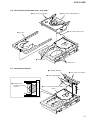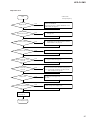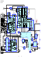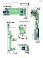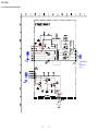
1
HCD-CL5MD
SERVICE MANUAL
AEP Model
UK Model
E Model
Australian Model
Ver 1.0 2001. 02
HCD-CL5MD is the tuner, deck, CD, MD and
amplifier section in CHC-CL5MD.
Model Name Using Similar Mechanism
CD
SECTION
MD
SECTION
TAPE DECK
SECTION
NEW
CD Mechanism Type
CDM63B
Base Unit Type
BU-30BD61
Optical Pick-up Type
A-MAX.3
Model Name Using Similar Mechanism
HCD-ZX50MD
MD Mechanism Type
MDM-7B
Optical Pick-up Type
KMS-260B/K1NP
Model Name Using Similar Mechanism
NEW
Tape Transport Mechanism Type
TCM-230ASR41CL
SPECIFICATIONS
Amplifier section
AEP model:
DIN power output (Rated): 40 + 40 watts
(6 ohms at 1 kHz, DIN)
Continuous RMS power output (Reference):
50 + 50 watts
(6 ohms at 1 kHz, 10%
THD)
Music power output (Reference):
95 + 95 watts
(6 ohms at 1 kHz, 10%
THD)
Other models:
DIN power output (Rated): 40 + 40 watts
(6 ohms at 1 kHz, DIN)
Continuous RMS power output (Reference):
50 + 50 watts
(6 ohms at 1 kHz, 10%
THD)
Inputs
VIDEO (AUDIO) IN (phono jacks):
voltage 250 mV,
impedance 47 kilohms
CD DIGITAL IN (Supported sampling frequencies:
32 kHz, 44.1 kHz and 48 kHz)
Outputs
PHONES (stereo minijack):
accepts headphones of
8 ohms or more.
SPEAKER:
accepts impedance of 6 to
16 ohms.
CD player section
System
Laser
Laser output
Frequency response
Compact disc and digital
audio system
Semiconductor laser
(λ=780 nm)
Emission duration:
continuous
Max. 44.6 µW*
* This output is the value
measured at a distance
of 200 mm from the
objective lens surface on
the Optical Pick-up
Block with 7 mm
aperture.
20 Hz – 20 kHz (±0.5 dB)
— Continued on next page —
MICRO HiFi COMPONENT SYSTEM
9-929-583-11
Sony Corporation
2001B1600-1
© 2001.2
Audio Entertainment Group
General Engineering Dept.
HCD-CL5MD
MD deck section
System
Laser
Sampling frequency
Frequency response
Tape deck section
Recording system
Frequency response
MiniDisc digital audio
system
Semiconductor laser
(λ=780 nm)
Emission duration:
continuous
44.1 kHz
20 Hz – 20 kHz (±0.5 dB)
4-track 2-channel stereo
40 – 13,000 Hz (±3 dB),
using Sony TYPE I
cassettes
Tuner section
FM stereo, FM/AM superheterodyne tuner
FM tuner section
Tuning range
87.5 – 108.0 MHz
(50 kHz step)
Aerial
FM lead aerial
Aerial terminals
75 ohms unbalanced
Intermediate frequency
10.7 MHz
AM tuner section
Tuning range
AEP model:
531 – 1,602 kHz
(with the interval set at
9 kHz)
Other models:
531 – 1,602 kHz
(with the interval set at
9 kHz)
530 – 1,710 kHz
(with the interval set at
10 kHz)
Aerial
AM loop aerial
External aerial terminals
Intermediate frequency
450 kHz
2
General
Power requirements
AEP model:
230 V AC, 50/60 Hz
Australian and New Zealand models:
230 – 240 V AC, 50/60
Hz
Other models:
120 V, 220 V, 230 – 240
V AC, 50/60 Hz
Adjustable with voltage
selector
Power consumption
AEP model:
100 watts
0.5 watts (at the Power
Saving Mode)
Other models:
100 watts
Dimensions (w/h/d) incl. projecting parts and controls
Amplifier/Tuner/Tape/MD/CD section:
Approx. 215 × 285 × 421
mm
Speaker:
Approx. 210 × 285 × 260
mm
Mass
Amplifier/Tuner/Tape/MD/CD section:
Approx. 8.6kg
Design and specifications are subject to change
without notice.
HCD-CL5MD
SELF-DIAGNOSIS FUNCTION
The self-diagnosis function consists of error codes for customers which are displayed automatically when errors occur, and error codes which
show the error history in the test mode during servicing. For details on how to view error codes for the customer, refer to the following box
in the instruction manual. For details on how to check error codes during servicing, refer to the following “Procedure for using the SelfDiagnosis Function (Error History Display Mode)”.
Self-diagnosis display
This system has a Self-diagnosis display
function to let you know if there is a system
malfunction. The display shows a code made
up of three letters and a message alternately to
show you the problem. To solve the problem
refer to the following list. If any problem
persists, consult your nearest Sony dealer.
C11/Protected
The MD is protected against erasure.
cRemove the MD and slide the tab to close the
slot (Refer to Operating Instruction on page 17).
C12/Cannot Copy
You tried to record a CD or MD with a format that
the system does not support, such as a CD-ROM.
cRemove the disc and turn off the system once,
then turn it on again.
C13/REC Error
Recording could not be performed properly.
cMove the system to a stable place, and start
recording over from the beginning.
The MD is dirty or scratched, or the MD does not
meet the standards.
cReplace the MD and start recording over from
the beginning.
C13/Read Error
The MD deck cannot read the disc information
properly.
cRemove the MD once, then insert it again.
C14/Toc Error
The MD deck cannot read the disc information
properly.
cReplace the MD.
cErase all the recorded contents of the MD using
the All Erase function (Refer to Operating
Instruction on page 27).
C41/Cannot Copy
The sound source is a copy of a commercially
available music software, or you tried to record a
CD-R (Recordable CD).
cThe Serial Copy Management System prevents
making a digital copy (Refer to Operating
Instruction on page 48). You cannot record a
CD-R.
E0001/MEMORY NG
There is an error in the internal data that the system
needs in order to operate.
cConsult your nearest Sony dealer.
E0101/LASER NG
There is a problem with the optical pickup.
cThe optical pickup may have failed. Consult your
nearest Sony dealer.
Procedure for using the Self-Diagnosis Function (Error History Display Mode).
Note: Perform the self-diagnosis function in the “error history display mode” in the test mode. The following describes the least required
procedure. Be careful not to enter other modes by mistake. If other modes are entered accidentally, press the MENU/NO button to
exit the mode.
1.
2.
3.
4.
5.
6.
7.
8.
9.
Connect the mains lead to the mains while pressing the DIMMER , FUNCTION , and x buttons together, then release the DIMMER,
FUNCTION , and x buttons simultaneously. While the test mode is set. “[Check]” will be displayed.
Move ./> left and right to display “[Service]” and press the ENTER/YES button.
Move ./> left and right to display “Err Display”.
Press the ENTER/YES button to enter the error history mode. “op rec tm” will be displayed.
Select the item to be displayed or executed using ./> .
Press the REC MODE button to display the selected item.
Press the REC MODE button another time to return to step 4.
Pressing the MENU/NO button displays “Err Display” and exits the error history display mode.
To exit the test mode, press the REPEAT button. This sets the standby state and ends the test mode.
3
HCD-CL5MD
ITEMS OF ERROR HISTORY MODE ITEMS AND CONTENTS
Selecting the Test Mode
Display
History
op rec tm
Displays the total recording time.
When the total recording time is more than 1 minute, displays the hour and minute
When less than 1 minute, displays “Under 1 min”
The display time is the time the laser is set to high power, which is about 1/4 of the actual recording time.
op play tm
Displays the total playback time.
When the total playback time is more than 1 minute, displays the hour and minute
When less than 1 minute, displays “Under 1 min”
spdl rp tm
Displays the total rotating time of the spindle motor.
When the total rotating time is more than 1 minute, displays the hour and minute
When less than 1 minute, displays “Under 1 min”
retry err
Displays the total number of retry errors during recording and playback
Displays “r xx p yy”. xx is the number of errors during recording. yy is the number of errors during playback.
This is displayed in hexadecimal from 00 to FF.
total err
Displays the total number of errors
Displays “total xx”. This is displayed in hexadecimal from 00 to FF.
err history
Displays the past ten errors.
Displays “0x ErrCd@@”.
X is the history number. The younger the number, the more recent is the history (00 is the latest). @@ is the error
code.
Select the error history number using ./> .
retry adrs
Displays the past five retry addresses.
Displays “xx ADRS yyyy”, xx is the history number, yyyy is the cluster with the retry error.
Select the error history number using ./> .
er refresh
Mode for erasing the error and retry address histories
Procedure
1. Press the REC MODE button when displayed as “er refresh”.
2. Press the ENTER/YES button when the display changes to “er refresh?”.
When “complete!” is displayed, it means erasure has completed.
Be sure to check the following after executing this mode.
*Data has been erased.
*Perform recording and playback, and check that the mechanism is normal.
op change
Mode for erasing the total time of op rec tm, op play tm.
These histories are based on the time of replacement of the optical pick-up. If the optical pick-up has been
replaced, perform this procedure and erase the history.
Procedure
1. Press the REC MODE button when displayed as “op change”.
2. Press the ENTER/YES button when the display changes to “op change?”.
When “Complete!” is displayed, it means erasure has completed.
spdl change
Mode for erasing the total spdl rp tm time
These histories are based on the time of replacement of the spindle motor. If the spindle motor has been replaced,
perform this procedure and erase the history.
Procedure
1. Press the REC MODE button when displayed as “spdl change”
2. Press the ENTER/YES button when the display changes to “spdl change?”
When “Complete!” is displayed, it means erasure has completed.
4
HCD-CL5MD
Table of Error Codes
Error Code
Description
10
Could not load
12
Loading switches combined incorrectly
20
Timed out without reading the top of PTOC
21
Could read top of PTOC, but detected error
22
Timed out without accessing UTOC
23
Timed out without reading UTOC
24
Error in UTOC
30
Could not start playback
31
Error in sector
40
Retry cause generated during normal recording
41
Retried in DRAM overflow
42
Retry occurred during TOC writing
43
Retry aborted during S.F editing
50
Other than access processing, and could not read address.
51
Focus NG occurred and overran.
5
HCD-CL5MD
TABLE OF CONTENTS
1. SERVICING NOTES ······················································· 7
2. GENERAL ·········································································· 9
3. DISASSEMBLY
3-1. Top Panel, Side Panel ·················································· 11
3-2. Cassette Mechanism ···················································· 12
3-3. Front Panel ·································································· 12
3-4. Panel Board ································································· 13
3-5. MD Mechanism ··························································· 13
3-6. Over Light Head (HR901), BD (MD) Board ·············· 14
3-7. Holder Assy ································································· 14
3-8. Loading Motor Assy (M103) ······································· 15
3-9. Sled Motor Assy (M102) ············································· 15
3-10. MD Optical Pick-Up (KMS-260B/K1NP) ·················· 16
3-11. Spindle Motor Assy ····················································· 16
3-12. Back Panel, Main Board ·············································· 17
3-13. Amp Board, Power Transformer ································· 17
3-14. CD Mechanism ···························································· 18
3-15. Relay Board ································································· 18
3-16. CD Base Unit (BU-30BD61) ······································ 19
3-17. CD Optical Pick-Up (A-MAX.3) ································ 19
3-18. BD (CD) Board ··························································· 20
3-19. Driver Board ································································ 20
3-20. Fitting Base (Stabilizer) Assy, Tray Assy ···················· 21
3-21. Tray Sensor Board ······················································· 21
3-22. Slider (Loading), Gear (Slider) ··································· 22
3-23. Stocker Assy ································································ 22
3-24. Disc Sensor Board ······················································· 23
3-25. IN OUT SW Board ······················································ 23
3-26. Motor Assy (M721), Motor Board ······························ 24
4. TEST MODE ···································································· 25
5. MECHANICAL ADJUSTMENTS ····························· 30
6. ELECTRICAL ADJUSTMENTS ······························· 30
7. DIAGRAMS
7-2. Block Diagram
CD Section ·································································· 47
MD Section ································································· 48
Syscon Section ···························································· 49
Main Section ······························································· 50
7-3. Printed Wiring Board Main Section ··························· 51
7-4. Schematic Diagram Main Section (1/2) ····················· 52
7-5. Schematic Diagram Main Section (2/2) ····················· 53
7-6. Schematic Diagram CD Section ································· 54
7-7. Printed Wiring Board CD Section ······························ 55
7-8. Schematic Diagram Driver Section ···························· 56
7-9. Printed Wiring Board Driver Section ························· 57
7-10. Schematic Diagram MD Section (1/2) ······················· 58
7-11. Schematic Diagram MD Section (2/2) ······················· 59
7-12. Printed Wiring Board MD Section ····························· 60
7-13. Printed Wiring Board Digital Section ························ 61
7-14. Schematic Diagram Digital Section (1/2) ·················· 62
7-15. Schematic Diagram Digital Section (2/2) ·················· 63
7-16. Schematic Diagram TC Section ································· 64
7-17. Printed Wiring Board TC Section ······························· 65
7-18. Schematic Diagram AMP Section ······························ 66
7-19. Printed Wiring Board AMP Section ··························· 67
7-20. Schematic Diagram Panel Section ····························· 68
7-21. Printed Wiring Board Panel Section ··························· 69
7-22. Schematic Diagram Trans Section ····························· 70
7-23. Printed Wiring Board Trans Section ··························· 71
7-24. Schematic Diagram Power Section ···························· 72
7-25. Printed Wiring Board Power Section ························· 73
7-26. IC Pin Functions ·························································· 75
7-27. IC Block Diagrams ······················································ 85
8. EXPLODED VIEWS
8-1.
8-2.
8-3.
8-4.
8-5.
8-6.
8-7.
8-8.
Side Panel, Back Panel Section ··································· 89
Front Panel Section ····················································· 90
Chassis Section ···························································· 91
MD Mechanism Deck Section-1 ································· 92
MD Mechanism Deck Section-2 ································· 93
CD Mechanism Deck Section-1 ·································· 94
CD Mechanism Deck Section-2 ·································· 95
Base Unit Section ························································ 96
7-1. Circuit Boards Location ·············································· 45
9. ELECTRICAL PARTS LIST ······································· 97
6
HCD-CL5MD
SECTION 1
SERVICING NOTES
NOTES ON HANDLING THE OPTICAL PICK-UP
BLOCK OR BASE UNIT
MODEL IDENTIFICATION
– Back Panel –
The laser diode in the optical pick-up block may suffer electrostatic
break-down because of the potential difference generated by the
charged electrostatic load, etc. on clothing and the human body.
During repair, pay attention to electrostatic break-down and also
use the procedure in the printed matter which is included in the
repair parts.
The flexible board is easily damaged and should be handled with
care.
FOR CD
NOTES ON LASER DIODE EMISSION CHECK
The laser beam on this model is concentrated so as to be focused on
the disc reflective surface by the objective lens in the optical pickup block. Therefore, when checking the laser diode emission,
observe from more than 30 cm away from the objective lens.
Power Voltage
Indicator
FOR MD
NOTES ON LASER DIODE EMISSION CHECK
Never look into the laser diode emission from right above when
checking it for adjustment. It is feared that you will lose your sight.
Model
AEP, UK models
Australian model
Laser component in this product is capable
of emitting radiation exceeding the limit for
Class 1.
Other models
Power Voltage
Incdication
AC: 230 V 50/60 Hz 100 W
AC: 230 – 240V 50/60 Hz 100 W
AC: 120 V, 220 V, 230 – 240V
50/60 Hz 100 W
To inspect the printed circuit boards, use the following
jigs.
• Extension jig to inspect the DIGITAL board
This appliance is classified as a CLASS 1 LASER product. The
CLASS 1 LASER PRODUCT MARKING is located on the rear
exterior.
This caution
label is
located inside
the unit.
Jig for extension between DIGITAL board CN1001 and MAIN
board CN701
Part code number: J-2501-019-A 1 pc
25 pins with 1.25 mm
• Extension jig to inspect the BD (CD) board (RELAY board)
Jig for extension between RELAY board CN2 and MAIN board
CN201
Part code number: J-2501-019-A 1 pc
25 pins with 1.25 mm
SAFETY-RELATED COMPONENT WARNING!!
CAUTION
Use of controls or adjustments or performance of procedures
other than those specified herein may result in hazardous radiation
exposure.
COMPONENTS IDENTIFIED BY MARK 0 OR DOTTED LINE WITH
MARK 0 ON THE SCHEMATIC DIAGRAMS AND IN THE PARTS
LIST ARE CRITICAL TO SAFE OPERATION. REPLACE THESE
COMPONENTS WITH SONY PARTS WHOSE PART NUMBERS
APPEAR AS SHOWN IN THIS MANUAL OR IN SUPPLEMENTS
PUBLISHED BY SONY.
Notes on chip component replacement
• Never reuse a disconnected chip component.
• Notice that the minus side of a tantalum capacitor may be
damaged by heat.
Flexible Circuit Board Repairing
• Keep the temperature of soldering iron around 270˚C
during repairing.
• Do not touch the soldering iron on the same conductor of the
circuit board (within 3 times).
• Be careful not to apply force on the conductor when soldering
or unsoldering.
7
HCD-CL5MD
JIG FOR CHECKING BD (MD) BOARD WAVEFORM
The special jig (J-2501-196-A) is useful for checking the waveform of the BD (MD) board. The names of terminals and the checking items
to be performed are shown as follows.
GND
I+3V
IOP
TE
VC
RF
FE
: Ground
: For measuring IOP (Check the deterioration of the optical pick-up laser)
: For measuring IOP (Check the deterioration of the optical pick-up laser)
: TRK error signal (Traverse adjustment)
: Reference level for checking the signal
: RF signal (Check jitter)
: Focus error signal
CN105
IOP
TE
I+3V
GND
FE
VC
RF
1
I+3V
IOP
GND
TE
FE
VC
RF
I+3V
Iop
GND
TE
FE
VC
RF
7
8
for
MDM-7B
HCD-CL5MD
SECTION 2
GENERAL
1
2
3
This section is extracted
from instruction manual.
123 4
4 5
6
wh
ws
wa
5
6
7
8
9
0
qa
qs
w;
qd
ql
qk
qf
qg
qj
qh
wh
7
wg
wg
wf
8
wd
ws
wa
w;
9
0
qa
wd
qs
qd
ql
qk
qj
BASS/TREBLE wf (40)
CD 1 – 3 qj (11)
CD 1 – 3 Z qj (9)
CD disc tray qk (9)
CD NX qs (9)
DIMMER 5 (7)
DISPLAY wg (8, 12, 16)
Display window 3
ENTER/START ws (17, 38)
ENTER/YES 7 (8, 11, 15, 20,
25, 34, 42)
FUNCTION qh (9, 14, 17, 25, 37)
GROOVE w; (40)
MD insertion slot wd (14)
MD REC ws (19)
MD NX qf (14)
MENU/NO 6 (24)
MUSIC MENU wf (41)
BUTTON DESCRIPTIONS
?/1 1
./> 4
Z9
x0
m/M wf
+/– wf
wf
qhqg qf
PHONES jack qd
PLAY MODE/DIRECTION wa
(9, 14, 17, 37)
REC MODE ws (20)
Remote sensor wh
REPEAT ql (10, 14)
STEREO/MONO ql (35)
SYNCHRO MODE ws (17)
Tape deck lid 2 (37)
TAPE REC PAUSE/START ws
(39)
TAPE nN qg (37)
TUNER/BAND qa (34)
VOLUME 8
CHECK 8 (11, 15)
CLEAR qs (11, 15)
CLOCK/TIMER SELECT 2
(42)
CLOCK/TIMER SET 3
(8, 42)
DBFB wh (40)
DIMMER wd (7)
DISC SKIP 9 (10)
DISPLAY qk (8, 12, 16)
ENTER/YES qa (8, 11, 15, 20,
25, 34, 42)
FUNCTION qg (9, 14, 17, 25, 37)
GROOVE qh (40)
MENU/NO wa (24)
MUSIC MENU 6 (41)
NAME EDIT/CHARACTER ws
(12, 25, 36)
REPEAT 7 (10, 14)
SCROLL wg (13, 26)
SLEEP 1 (41)
SURROUND 5 (40)
TUNER/BAND wf (34)
VOL +/– qj
BUTTON DESCRIPTIONS
@/1 4
N q;
x q;
X q;
M qd
> qf
. ql
m w;
9
HCD-CL5MD
Setting the time
1 Turn on the system.
2 Press CLOCK/TIMER SET on the
remote.
Proceed to step 5 when you set the clock for
the first time.
3 Turn ./> (or press . or > on
the remote) to select “CLOCK SET?”.
4 Press ENTER/YES.
5 Turn ./> (or press . or > on
the remote) to set the hour.
6 Press ENTER/YES or M.
The minute indication flashes.
7 Turn ./> (or press . or > on
the remote) to set the minute.
8 Press ENTER/YES.
The clock starts working.
If you made a mistake
Press m or M repeatedly until the incorrect
item flashes, then set it again.
To change the preset time
Start over from step 1.
10
Saving the power in
standby mode
Press DISPLAY repeatedly when the
system is off. Each time you press the
button, the system switches cyclically as
follows:
Demonstration t Clock display t Power
Saving Mode
To cancel the Power Saving Mode
Press DISPLAY once to show the
demonstration, twice to show the clock display
Tip
?/1 indicator lights up even in the Power Saving
Mode.
HCD-CL5MD
SECTION 3
DISASSEMBLY
• The equipment can be removed using the following procedure.
Set
Top panel, Side panel
Cassette mechanism
Front panel
Back panel, Main board
Panel board
Amp board,
Power transformer
MD mechanism
CD mechanism
Relay board
Over light head (HR901),
BD (MD) board
CD base unit (BU-30BD61)
Holder assy
CD optical pick-up
(A-MAX.3)
Loading motor assy (M103)
Driver board
Fitting base (stabilizer) assy,
Tray assy
BD (CD) board
Sled motor assy (M102)
Tray sensor board
MD optical pick-up
(KMS-260B/K1NP)
Slider (loading), Gear (slider)
Stocker assy
Spindle motor assy
Disc sensor board
IN OUT SW board
Motor assy (M721), Motor board
Note : Follow the disassembly procedure in the numerical order given.
3-1. TOP PANEL, SIDE PANEL
Note: Attach it so that it pressed down
the Main board.
q; Screw
(+BVTT 3 × 8)
qs Side panel (L)
(Remove in the direction
of the arrow)
qh Top panel
(Remove in the direction
of the arrow)
qa Four screws
(CASE 3 TP2)
qf Flact cable (9 core)
(CN304)
1 Screw
(+BVTT 3 × 8)
qg Connector
(CN305)
5 Two screws
(+BVTP 3 × 8)
6 D.C. Fan
2 Two screws
(+BVTT 3 × 8)
4 Heat sink, cover
qd Two screws
(HEXAGON
SOCKET TAPPING)
3 Connector
(CN904)
7 Screw
(+BVTT 3 × 8)
9 Side panel (R)
(Remove in the direction
of the arrow)
8 Four screws
(CASE 3 TP2)
11
HCD-CL5MD
3-2. CASSETTE MECHANISM
4 Two screws
(+BVTP 3 × 8)
5 TC board
7 Flat cable (9 core)
9 Two screws
8 Cassette mechanism deck
1 Connector
6 Screw
(+BVTP 2.6 × 8)
6 Two screws
(+BVTP 2.6 × 8)
3 Bracket
(Cassette mechanism)
qs F/R belt
qa Main belt
2 Screw
(+BVTP 2.6 × 8)
q; Motor
2 Three screws
(+BVTP 2.6 × 8)
3-3. FRONT PANEL
1 Screw
(+BVTP 3 × 8)
8 Front panel
4 Screw
(+BVTP 3 × 8)
5 Two screws
(HEXAGON
SOCKET TAPPING)
3 Flact cable (25 core)
(CN701)
7 Connector
(CN701)
5 Screw
(+BVTP 3 × 8)
12
2 Screw
(+BVTP 3 × 8)
HCD-CL5MD
3-4. PANEL BOARD
3 Two screws
(+BVTP 3 × 8)
4 Shield (MD)
8 Six screws
(+BVTP 2.6 × 8)
7 Four screws
(+BVTP 2.6 × 8)
9 Panel board
1 Two screws
(+BVTP 2.6 × 8)
q; Two screws
(+BVTP 2.6 × 8)
2 MD mechanism
qa Ring SW board
8 Eight screws
(+BVTP 2.6 × 8)
6 Nut
5 Knob (vol)
3-5. MD MECHANISM
3 Two screws
(+BVTP 3 × 8)
4 Digital board
7 Two insulators
5 Two screws
(+BVTTWH M3)
2 Flat cable (17 core)
(CN103)
1 Flat cable (27 core)
(CN102)
5 Two screws
(+BVTTWH M3)
6 MD mechanism
(MDM-7B)
7 Two insulators
13
HCD-CL5MD
3-6. OVER LIGHT HEAD (HR901), BD (MD) BOARD
2 Screw (P 1.7 × 6)
3 Over light head (HR901)
4 Remove the solder (four portions).
8 BD (MD) board
6
1 Connector (CN104)
7 Flexible board (CN101)
4 Remove the solder (five portions).
5 Screw (2 × 6)
3-7. HOLDER ASSY
2 Claw
5 Holder assy
4
1 Tension spring (holder)
14
3
HCD-CL5MD
3-8. LOADING MOTOR ASSY (M103)
1 Belt (loading)
2 Two screws (+PWH1.7 × 3.5)
3 Loading motor assy (M103)
3-9. SLED MOTOR ASSY (M102)
3
4 Slider (EJ)
7 Slider
6 Claw
5 Lever (head)
2 Guide (L)
1 Two screws (CZN2 × 6)
9 Two screws (+PWH1.7 × 3.5)
8 Lever (CHG)
q; Sled motor assy (M102)
15
HCD-CL5MD
3-10. MD OPTICAL PICK-UP (KMS-260B/K1NP)
qa MD Optical pick-up (KMS-260B/K1NP)
7 Main shaft
1 Flexible PWB
q; SL base
9 Screw (+P1.7 × 6)
8
6 Two screws (+KPT2 × 6)
4 Screw (CZN2 × 6)
5 Base (BU-A)
3 Gear (SD)
2 Screw (M1.7, TAPPING)
3-11. SPINDLE MOTOR ASSY
2 Spindle motor assy (M101)
1 Three screws (M1.7, TAPPING)
16
HCD-CL5MD
3-12. BACK PANEL, MAIN BOARD
3 Blacket (Heat sink)
5 Back panel
2 Two screws
(+BVTP 3 × 8)
7 Tuner
1 Flat cable (15 core)
(CN502)
Main board
6 Two screws
(+BVTP 3 × 8)
4 Thirteen screws
(+BVTP 3 × 8)
9 Connector
(CN701)
8 Two connector
(CN101, CN251)
q; Main board
3-13. AMP BOARD, POWER TRANSFORMER
5 Two screws
(+BVTP 3 × 16)
3 Four screws
(+BVTT 4 × 8)
4 Power
transformer
8 Two screws
(+BVTP 3 × 8)
9 Heat sink
6 Three screws
(+BVTP 3 × 8)
7 Amp board
q; Two screws
(+BVTP 3 × 8)
2 Connector
(CN902)
1 Connector
(CN901)
qs Cord bushing
qa Sub power board
17
HCD-CL5MD
3-14. CD MECHANISM
5 CD mechanism deck
(CDM63B)
3 Chassis assy
2 Two screws
(+BVTP 3 × 8)
1 Three screws
(+BVTP 3 × 8)
4 Four screws
(+BVTP 3 × 8)
Note: When installing the CD mechanism, the four bosses
must be aligned with the specified positions.
3-15. RELAY BOARD
1 Flat cable (21 core)
(CN792)
3 RELAY board
2 Two Screws
(+BTTP M2.6)
18
HCD-CL5MD
3-16. CD BASE UNIT (BU-30BD61)
q; Insulator
9 Cone coil spring
qa CD base unit
(BU-30BD61)
8 Floating screw (DIA.12)
q; Two Insulators
q; Insulator
4 Two coil springs (Insulators)
7 Coil spring (Insulator)
6 Washer
3 Two stoppers
5 Floating screw (PTPWH M2.6)
1 Flat cable (22 core)
(CN101)
2 Two screws (BVTP2.6 × 8)
3-17. CD OPTICAL PICK-UP (A-MAX.3)
3 MD Optical pick-up (A-MAX.3)
1 Flat cable (16 core)
2 Sled shaft
19
HCD-CL5MD
3-18. BD (CD) BOARD
4 Gear (LA)
5 Gear (LB)
1 Flat cable (16 core) (CN102)
3 BD (CD) board
2 Remove the solder
(four portions).
3-19. DRIVER BOARD
3 DRIVER board
1 Connector (CN703)
1 Connector (CN704)
1 Connector (CN702)
2 Screw (BTTP M2.6)
2 Screw (BTTP M2.6)
1 Connector (CN705)
20
HCD-CL5MD
3-20. FITTING BASE (STABILIZER) ASSY, TRAY ASSY
1 Two screws (+BTTP M2.6)
4 Fitting base (STABILIZER) assy
2
2
1 Two screws (+BTTP M2.6)
5 Tray assy
3 Three bosses
3 Three bosses
3-21. TRAY SENSOR BOARD
6 HOLDER (SENSOR)
2 Two screws (+BTTP M2.6)
5 TRAY SENSOR board
Cam
1 Rotate the cam,
and lift up the stocker
at the full.
4 Two screws (+BTTP M2.6)
Stocker
3
21
HCD-CL5MD
3-22. SLIDER (LOADING), GEAR (SLIDER)
3 Two screws (+BTTP M2.6)
4 Bracket (retainer)
2 Bracket (retainer)
1 Two screws (+BTTP M2.6)
6 Slider (LOADING)
8 Two gears (SLIDER)
5 Floating screw
7 Two floating screws
3-23. STOCKER ASSY
3 Stocker assy
1 Screw (+BTTP M2.6)
A
A
2 Slide the slider (BU.L),
slider (BU.R) in the direction of
arrow A at the full.
22
1 Screw (+BTTP M2.6)
HCD-CL5MD
3-24. DISC SENSOR BOARD
2 CD base unit assy
1
4 DISC SENSOR board
3 Two screws (+BTTP M2.6)
3-25. IN OUT SW BOARD
2 Two screws (+BTTP M2.6)
3 IN OUT SW board
1 Connector (CN704)
23
HCD-CL5MD
3-26. MOTOR ASSY (M721), MOTOR BOARD
1 Belt
2 Connector (CN702)
6
Motor board bottom view
7 Motor assy (M721)
3 Remove two solders.
4 Two screws (+BTTP M2.6)
5 Motor board
24
SECTION 4
TEST MODE
[CD Ship Mode]
• This mode moves the optical pick-up to the position durable to
vibration. Use this mode when returning the set to the customer
after repair.
Procedure:
1. Press ?/1 button to turn the set ON.
2. Press CD 1 button and FUNCTION button simultaneously.
3. After the “STANDBY” display blinks six times, a message
“LOCK” is displayed on the fluorescent indicator tube, and the
CD ship mode is set.
[GC Test Mode]
• This mode is used to check the software version, FL tube, LED,
keyboard and VACS.
Procedure:
1. Press three buttons x , DISPLAY , and CD 2 simultaneously.
2. LEDs and fluorescent indicator tube are all turned on.
3. When you want to enter the software version display mode,
press CD 1 . The model number and destination are displayed.
4. Each time CD 1 is pressed, the display changes starting from
MC version, GC version, CD version, CDD version, CDM
version, BD version, ST version, TA version, TM version, TC
version and MD version in this order, and returns to the model
number and destination display.
5. Press CD 2 button, and the key check mode is activated.
6. In the key check mode, the fluorescent indicator tube displays
“K 0 J 0 V 0”. Each time a button is pressed, “K 0” value
increases. However, once a button is pressed, it is no longer
taken into account.
“V 0” value increases like 1, 2, 3 ... if rotating VOLUME knob
in “+” direction, or it decreases like 0, 9, 8 ... if rotating in
“–” direction.
7. Also when CD 3 is pressed after lighting of all LEDs and FL
tubes, value of VACS appears.
8. To exit from this mode, press three buttons in the same manner
as step 1, or disconnect the power cord.
[MC Test Mode]
• This mode is used to check operations of the respective sections
of Amplifier, Tuner, CD and Tape.
Procedure:
1. Press the ?/1 button to turn on the set.
2. Press the three buttons of x , DISPLAY and CD 3
simultaneously.
3. The “VOLUME” segment flashes.
4. Every pressing of BASS/TREBLE f changes the displays in
the order of “GEQ MIN”t“GEQ FLAT”t“GEQ MAX”
5.
6.
7.
8.
HCD-CL5MD
When x button is pressed to stop recording, the Tape (Deck)
B is selected and tape is rewound using the m button, tape
is rewound, tape is stops at around the record-starting position
and playback of the recorded portion of the tape is started. If
PAUSE is inserted even once during recording, tape is rewound
to the position around the PAUSE position and is played back.
10. The cold reset is enforced at the same time.
9.
[CD Service Mode]
• This mode can run the CD sled motor freely. Use this mode, for
instance, when cleaning the optical pick-up.
Procedure:
1. Press ?/1 button to turn the set ON.
2. Select the function “CD”.
3. Press three buttons x , FUNCTION , and CD 2 simultaneously.
4. The CD service mode is selected.
5. With the CD in stop status, turn the shuttle knob clockwise to
move the optical pick-up to outside track, or turn the shuttle
knob counter-clockwise to inside track.
6. To exit from this mode, perform as follows:
1) Move the optical pick-up to the most inside track.
2) Press three buttons in the same manner as step 2.
Note: • Always move the optical pick-up to most inside track when exiting from this mode. Otherwise, a disc will not be unloaded.
• Do not run the sled motor excessively, otherwise the gear can be
chipped.
[CD Ship (Memory Clear) Mode]
• Set the CD ship mode and set the default setup when shipped
from the factory at the next AC power on.
Procedure:
1. Press ?/1 button to turn the set ON.
2. Select the function “CD ”.
3. Press three buttons x , FUNCTION and CD 1 simultaneously.
4. After the “STANDBY” display blinks six times, a message
“LOCK” is displayed on the fluorescent indicator tube, and the
CD ship mode is set.
[CD/MD/TAPE Repeat 5 Times Limit Release Mode]
• 5 times limit of repeating CD/MD/TAPE is released.
Procedure:
1. Press ?/1 button to turn the set ON.
2. Press three buttons x , FUNCTION and CD 1Z .
3. 5 times limit of repeating CD/MD/TAPE is released.
4. Cold reset is performed at power off.
When the VOLUME control knob is turned clockwise even
slightly, the sound volume increases to its maximum and a
message “VOLUME MAX” appears for two seconds, then the
display returns to the original display.
When the VOLUME control knob is turned counter-clockwise
even slightly, the sound volume decreases to its minimum and
a message “VOLUME MIN” appears for two seconds, then
the display returns to the original display.
In the test mode, the default-preset channel is called even when
the TUNER is selected and an attempt is made to call the preset
channel that has been stored in memory, by operating the Shuttle
knob. (It means that the memory is cleared.)
When a tape is inserted in Deck B and recording is started, the
input source function selects VIDEO automatically.
25
HCD-CL5MD
4-1. PRECAUTIONS FOR USE OF TEST MODE
• As loading related operations will be performed regardless of the test mode operations being performed, be sure to check that the disc
is stopped before setting and removing it.
Even if the Z button is pressed while the disc is rotating during continuous playback, continuous recording, etc., the disc will not stop
rotating.
Therefore, it will be ejected while rotating.
Be sure to press the MENU/NO button, and press the Z button after the disc stops rotating.
4-1-1. Recording laser emission mode and operating buttons
•
•
•
•
•
•
•
•
Continuous recording mode (CREC 1MODE) (C35)
Laser power check mode (LDPWR CHECK) (C13)
Laser power adjustment mode (LDPWR ADJUS) (C04)
Iop check (Iop Compare) (C27)
Iop value nonvolatile writing (Iop NV Save) (C06)
Traverse (MO) check (EF MO CHECK) (C14)
Traverse (MO) adjustment (EF MO ADJUS) (C07)
When pressing the MD REC button.
4-2. SETTING THE TEST MODE
The following are two methods of entering the test mode.
Procedure: Connect the mains lead to the mains while pressing the DIMMER , FUNCTION , and x buttons together, then release the
DIMMER , FUNCTION , and x buttons simultaneously.
When the test mode is set, “[Check]” will be displayed. Move ./> to switch between the following three groups;
··· y Check y Service y Develop y ···.
NOTE: Do not use the test mode in the [Develop] group.
If used, the unit may not operate normally.
If the [Develop] group is set accidentally, press the MENU/NO button, immediately to exit the [Develop] group.
4-3. EXITING THE TEST MODE
Press the REPEAT button. The disc is ejected when loaded, and “Initialize” display blinks, and the STANDBY state is set.
4-4. BASIC OPERATIONS OF THE TEST MODE
Operate using the ./> , ENTER/YES button, REC MODE button, MENU/NO button.
Function name
Function
MENU/NO button
Cancel or move to top hierarchy
ENTER/YES button
Set
./> (Left or Right)
Select
REC MODE button
Set submenu
26
HCD-CL5MD
4-5. SELECTING THE TEST MODE
There are 26 types of test modes as shown below. The groups can be switched by moving ./> . After selecting the group to be used,
press the ENTER/YES button. After setting a certain group, move the multi-stick to switche between these modes.
Refer to “Group” in the table for details selected.
All adjustments and checks during servicing can be performed in the test mode in the Service group.
NOTE: Do not use the test mode in the [Develop] group.
If used, the unit may not operate normally.
If the [Develop] group is set accidentally, press the MENU/NO button, immediately to exit the [Develop] group.
Group
Display
No.
Details
AUTO CHECK
C01
Automatic self-diagnosis
Err Display
C02
Error history display, clear
TEMP ADJUS
C03
Temperature compensation offset adjustment
LDPWR ADJUS
C04
Laser power adjustment
Iop Write
C05
Iop data writing
Iop NV Save
C06
Writes current Iop value in read nonvolatile memory using microprocessor
EF MO ADJUS
C07
Traverse (MO) adjustment
EF CD ADJUS
C08
Traverse (CD) adjustment
FBIAS ADJUS
C09
Focus bias adjustment
AG Set (MO)
C10
Focus, tracking gain adjustment (MO)
AG Set (CD)
C11
Focus, tracking gain adjustment (CD)
TEMP CHECK
C12
Temperature compensation offset check
LDPWR CHECK
C13
Laser power check
EF MO CHECK
C14
Traverse (MO) check
EF CD CHECK
C15
Traverse (CD) check
FBIAS CHECK
C16
Focus bias check
ScurveCHECK
C17
S-curve check
VERIFYMODE
C18
Nonvolatile memory check
DETRK CHECK
C19
Detrack check
0920 CHECK
C25
Most circumference check
Iop Read
C26
Iop data display
Iop Compare
C27
Comparison with initial Iop value written in nonvolatile memory
ADJ CLEAR
C28
Initialization of nonvolatile memory for adjustment values
INFORMATION
C31
Display of microprocessor version, etc.
CPLAY1MODE
C34
Continuous playback mode
CREC 1MODE
C35
Continuous recording mode
Mark
Check
Service
• For details of each adjustment mode, refer to “6. Electrical Adjustments”.
For details of “Err Display”, refer to “Self-Diagnosis Function” on page 3.
• If a different mode has been selected by mistake, press the MENU/NO button, to exit that mode.
• Modes with (X) in the Mark column are not used for servicing and therefore are not described in detail. If these modes are set accidentally, press the MENU/NO button, to exit the mode immediately.
27
HCD-CL5MD
4-5-1. Operating the Continuous Playback Mode
1. Entering the continuous playback mode
1 Set the disc in the unit. (Whichever recordable discs or discs for playback only are available.)
2 Move ./> and display “CPLAY1MODE”(C34).
3 Press the ENTER/YES button to change the display to “CPLAY1MID”.
4 When access completes, the display changes to “C =
AD = ”.
Note : The numbers “ ” displayed show you error rates and ADER.
2. Changing the parts to be played back
1 Press the ENTER/YES button during continuous playback to change the display as below.
“CPLAY1MID” t “CPLAY1OUT” t “CPLAY1IN”
When pressed another time, the parts to be played back can be moved.
2 When access completes, the display changes to “C =
AD = ”.
Note : The numbers “ ” displayed show you error rates and ADER.
3. Ending the continuous playback mode
1 Press the MENU/NO button. The display will change to “CPLAY1MODE”(C34).
2 To remove the disc, press the Z button.
Note : The playback start addresses for IN, MID, and OUT are as follows.
IN
40h cluster
MID 300h cluster
OUT 700h cluster
4-5-2. Operating the Continuous Recording Mode (Use only when performing self-recording/palyback check.)
1. Entering the continuous recording mode
1 Set a recordable disc in the unit.
2 Move ./> and display “CREC 1MODE” (C35).
3 Press the ENTER/YES button to change the display to “CREC 1MID”.
4 When access completes, the display changes to “CREC1 (
)” and REC lights up.
Note : The numbers “ ” displayed shows you the recording position addresses.
2. Changing the parts to be recorded
1 When the ENTER/YES button is pressed during continuous recording, the display changes as below.
“CREC 1MID” t “CREC 1OUT” t “CREC 1IN”
When pressed another time, the parts to be recorded can be changed. REC goes off.
)” and REC lights up.
2 When access completes, the display changes to “CREC 1(
Note : The numbers “ ” displayed shows you the recording position addresses.
3. Ending the continuous recording mode
1 Press the MENU/NO button. The display changes to “CREC 1MODE” (C35 ) and REC goes off.
2 To remove the disc, press the Z button.
Note 1 : The recording start addresses for IN, MID, and OUT are as follows.
IN
40h cluster
MID 300h cluster
OUT 700h cluster
Note 2 : Press the MENU/NO button can be used to stop recording anytime.
Note 3 : Do not perform continuous recording for long periods of time above 5 minutes.
Note 4 : During continuous recording, be careful not to apply vibration.
4-6. FUNCTIONS OF OTHER BUTTONS
Function
PLAY
Contents
Sets continuous playback when pressed in the STOP state. When pressed during continuous
playback, the tracking servo turns ON/OFF.
MD 7
Stops continuous playback and continuous recording.
J (FF)
The sled moves to the outer circumference only when this is pressed.
j (FR)
The sled moves to the inner circumference only when this is pressed.
PLAY MODE
Switches the spindle servo mode (CLV S y CLV A).
EJECT
Ejects the disc.
REPEAT
Exits the test mode. (When No disc)
28
HCD-CL5MD
4-7. MEANINGS OF OTHER DISPLAYS
Contents
Display
When Lit
When Off
LP2
Servo ON
Servo OFF
LP4
Tracking servo OFF
Tracking servo ON
(LED)
Recording mode ON
Recording mode OFF
SYNC
CLV low speed mode
CLV normal mode
LEVEL-SYNC
ABCD adjustment completed
OVER
Tracking offset cancel ON
TOC
Tracking auto gain OK
REPEAT
Focus auto gain OK
X1
CLV S
CLV A
MONO
CLV LOCK
CLV UNLOCK
Tracking offset cancel OFF
4-8. AUTOMATIC SELF-DIAGNOSIS FUNCTION
This test mode performs CREC and CPLAY automatically for mainly checking the characteristics of the optical pick-up.
To perform this test mode, the laser power must first be checked.
Perform AUTO CHECK after the laser power check and Iop check.
Procedure
1. Press the ENTER/YES button. If “LDPWR” is displayed, it means that the laser power check has not been performed. In this case,
perform the laser power check and Iop compare, and then repeat from step 1.
2. If a disc is in the mechanical deck, it will be ejected forcibly.
“DISC IN” will be displayed in this case. Load a test disc (MDW-74/GA-1) which can be recorded.
3. If a disk is loaded at step 2, the check will start automatically.
4. When “XX CHECK” is displayed, the item corresponding to XX will be performed.
When “06 CHECK” completes, the disc loaded at step 2 will be ejected. “DISC IN” will be displayed. Load the check disc (MD) TDYS-1.
5. When the disc is loaded in step 4, the check will automatically be resumed from “07 CHECK”.
6. After completing to test item 12, check OK or NG will be displayed. If all items are OK, “CHECK ALL OK” will be displayed. If any
item is NG, it will be displayed as “NG:xxxx”.
When “CHECK ALL OK” is displayed, it means that the optical pick-up is normal. Check the operations of the other spindle motor, thread
motor, etc.
When displayed as “NG:xxxx”, it means that the optical pick-up is faulty. In this case, replace the optical pick-up.
4-9. INFORMATION
Display the software version.
Procedure
1. If displayed as “INFORMATION”, press the ENTER/YES button.
2. The software version will be displayed.
3. Press the MENU/NO button is lit to end this mode.
4-10. WHEN MEMORY NG IS DISPLAYED
If the nonvolatile memory data is abnormal, “E001”/”MEMORY NG” will be displayed so that the MD deck does not continue operations.
In this case, set the test mode promptly and perform the following procedure.
Procedure
1. Set the test mode. (Refer to 4-2.)
2. Normally a message for selecting the test mode will be displayed. However if the nonvolatile memory is abnormal, the following will be
displayed. “INIT EEP?”
3. Press the x button and Z button together.
4. Move ./> and select MDM-7B.
5. Press the REC MODE button. If the nonvolatile memory is successfully overwritten, the normal test mode will be set and a message
to select the test mode will be displayed.
29
HCD-CL5MD
SECTION 5
MECHANICAL ADJUSTMENTS
Precaution
1. Clean the following parts with a denatured alcohol-moistened
swab:
record/playback heads
pinch rollers
erase head
rubber belts
capstan
idlers
2. Demagnetize the record/playback head with a head demagnetizer.
3. Do not use a magnetized screwdriver for the adjustments.
4. After the adjustments, apply suitable locking compound to the
parts adjusted.
5. The adjustments should be performed with the rated power supply voltage unless otherwise noted.
Torque Measurement
Mode
FWD
FWD
back tension
REV
REV
back tension
Torque meter
CQ-102C
CQ-102C
CQ-102RC
CQ-102RC
FF/REW
CQ-201B
FWD tension
CQ-403A
REV tension
CQ-403R
Meter reading
3.04 – 6.96 N • m
(31 to 71 g • cm)
(0.43 – 0.98 oz • inch)
0.20 – 0.58 N • m
(2 to 6 g • cm)
(0.02 – 0.08 oz • inch)
3.04 – 6.96 N • m
(31 to 71 g • cm)
(0.43 – 0.98 oz • inch)
0.20 – 0.58 N • m
(2 to 6 g • cm)
(0.02 – 0.08 oz • inch)
6.97 – 14.02 N • m
(71 to 143 g • cm)
(0.98 – 1.99 oz • inch)
0.98 N • m or more
(100 g or more)
(3.53 oz or more)
0.98 N • m or more
(100 g or more)
(3.53 oz or more)
SECTION 6
ELECTRICAL ADJUSTMENTS
DECK SECTION
0 dB=0.775V
1. Demagnetize the record/playback head with a head demagnetizer.
2. Do not use a magnetized screwdriver for the adjustments.
3. After the adjustments, apply suitable locking compound to the
parts adjusted.
4. The adjustments should be performed with the rated power supply voltage unless otherwise noted.
5. The adjustments should be performed in the order given in this
service manual. (As a general rule, playback circuit adjustment
should be completed before performing recording circuit adjustment.)
6. The adjustments should be performed for both L-CH and R-CH.
7. Switches and controls should be set as follows unless otherwise
specified.
Tape
Signal
P-4-A100
10 kHz, –10 dB
Azimuth Adjustment
WS-48B
3 kHz, 0 dB
Tape Speed Adjustment
Used for
Record/Playback Head Azimuth Adjustment
Procedure:
1. Mode : Playback
test tape
P-4-A100
(10kHz, –10dB)
main board
CN301
Pin 1 (L-ch)
Pin 3 (R-ch)
set
level meter
+
–
2. Turn the adjustment screw and check output peaks. If the peaks
do not match for L-CH and R-CH, turn the adjustment screw so
that outputs match within 1 dB of peak.
L-CH
peak
screw
position
output
level
within
1 dB
within 1dB
R-CH
peak
L-CH
peak
30
R-CH
peak
screw
position
HCD-CL5MD
Record Bias Adjustment
3. Mode: Playback
test tape
P-4-A100
(10kHz, –10dB)
Procedure:
main board
CN301
Pin 1 (L-ch)
oscilloscope
Pin 2 (GND)
L
set
R
Pin 3 (R-ch)
INTRODUCTION
When set to the test mode performed in Tape Speed Adjustment, when the tape is rewound after recording, the “REC memory
mode” which rewinds only the recorded portion and playback is
set.
This “REC memory mode” is convenient for performing this adjustment. During recording, the input signal FUNCTION will automatically switch to VIDEO.
(After recording, press the m button without stopping will return to the position where recording was started.)
Waveform of oscilloscope
in phase
45°
90°
good
135°
180°
wrong
1. Press FUNCTION button to select VIDEO. (This step is not
necessary if the above test mode has already been set.)
2. Insert a tape into deck, press the TAPE REC PAUSE/START
button, and then press the Y button to start recording.
3. Mode: Record
VIDEO (AUDIO) IN
1) 315 Hz
} 50 mV (–23.8 dB)
2) 10 kHz
4. After the adjustments, apply suitable locking compound to the
parts adjusted.
AF OSC
Adjustment Location: Record/Playback/Erase Head
blank tape
CS-123
600 Ω
attenuator
set
Tape Speed Check
Note: Set the test mode using the following method and begin tape
speed adjustment.
Procedure:
With the power turned ON, press the x button, ENTER/YES
button, and DISC 3 button simultaneously.
(The “VOLUME” on the fluorescent display tube will blink while
in the test mode.)
To exit the test mode, press the "/1 button.
1. Insert the WS-48B into deck.
2. Press the Y button of deck.
3. Check the reading of frequency counter becomes 3000 ± 15 Hz.
Sample Value of Wow and flutter
W.RMS (JIS) less than 0.3%
(test tape: WS-48B)
4. Mode: Playback
recorded
position
level meter
set
main board
CN301
Pin 3 (R-ch)
Pin 1 (L-ch)
5. Confirm playback the signal recorded in step 2 become adjustment level as follows.
If these levels do not adjustment level, adjust the RV304 (L-CH)
and RV354 (R-CH) on the TC board to repeat steps 3 and 4.
Adjustment level: The playback output of 10 kHz level difference
against 315 Hz reference should be 0 ± 0.5 dB.
Adjustment Location:
[TC BOARD]
RV304
RV354
RV304(Lch),RV354(Rch)
Record Bias
31
HCD-CL5MD
Record Level Adjustment
CD SECTION
Procedure:
Note :
INTRODUCTION
When set to the test mode performed in Tape Speed Adjustment, when the tape is rewound after recording, the “REC memory
mode” which rewinds only the recorded portion and playback is
set.
This “REC memory mode” is convenient for performing this
adjustment. During recording, the input signal FUNCTION will
automatically switch to VIDEO.
(After recording, press the m button without stopping will return to the position where recording was started.)
1. Press FUNCTION button to select VIDEO. (This step is not
necessary if the above test mode has already been set.)
2. Insert a tape into deck, press the TAPE REC PAUSE/START
button, and then press the Y button to start recording.
3. Mode: Record
VIDEO (AUDIO) IN (J101)
315Hz 50 mV (–23.8 dB)
AF OSC
blank tape
CS-123
600 Ω
attenuator
set
1. CD Block is basically designed to operate without adjustment.
Therefore, check each item in order given.
2. Use YEDS-18 disc (3-702-101-01) unless otherwise indicated.
3. Use an oscilloscope with more than 10MΩ impedance.
4. Clean the object lens by an applicator with neutral detergent
when the signal level is low than specified value with the
following checks.
S-Curve Check
Oscilloscope
BD (CD) board
TP(FEO)
TP(DVC)
Procedure :
1. Connect oscilloscope to TP (FEO).
2. Connect between TP (FEI) and TP (VC) by lead wire.
3. Turn Power switch on.
4. Load a disc (YEDS-18) and actuate the focus search. (In
consequence of open and close the disc tray, actuate the focus
search)
5. Confirm that the oscilloscope waveform (S-curve) is
symmetrical between A and B. And confirm peak to peak level
within 4 ±1 Vp-p.
S-curve waveform
4. Mode: Playback
symmetry
recorded
position
level meter
A
within 4 ±1Vp-p
set
main board
CN301
Pin 3 (R-ch)
Pin 1 (L-ch)
5. Confirm playback the signal recorded in step 2 become adjustment level as follows.
If these levels do not adjustment level, adjust the RV301 (L-CH)
and RV351 (R-CH) on the MAIN board to repeat steps 3 and 4.
B
7. After check, remove the lead wire connected in step 2.
Note : • Try to measure several times to make sure than the ratio
of A : B or B : A is more than 10 : 7.
• Take sweep time as long as possible and light up the
brightness to obtain best waveform.
RF Level Check
Adjustment level:
CN301 playback level: 47.2 to 53.0 mV (–24.3 to –23.3 dB)
Adjustment Location:
oscilloscope
BD board
TP(RFAC)
TP(DVC)
[MAIN BOARD]
IC301
RV351
Record Level (R ch)
32
CN301
RV301
Record Level (L ch)
Procedure :
1. Connect oscilloscope to TP (RFAC).
2. Turned Power switch on.
3. Load a disc (YEDS-18) and playback.
4. Confirm that oscilloscope waveform is clear and check RF signal
level is correct or not.
5. Measure the RFDC in the same way.
HCD-CL5MD
Note: Clear RF signal waveform means that the shape “◊” can be
clearly distinguished at the center of the waveform.
Adjustment Location :
[ BD (CD) BOARD ] — SIDE B —
RF signal waveform
VOLT/DIV : 200mV
TIME/DIV : 500ns
level : 1.1 ± 0.3Vp-p
E-F Balance (1 Track jump) Check
TP
(CE)
oscilloscope
BD (CD) board
TP (TEO)
TP (DVC)
TP
(RFDC)
+
–
IC101
IC103 TP
(RFAC)
TP
(XPCK)
Procedure:
1. Connect oscilloscope to TP (TEO) and TP (DVC) board.
2. Turned Power switch on.
3. Load a disc (YEDS-18) and playback the number five track.
4. Press the u button. (Becomes the 1track jump mode.)
5. Confirm that the level B and A (DC voltage) on the oscilloscope
waveform.
1 track jump waveform
Center of
waveform
B
A (DC voltage)
0V
Symmetry
level=1.3 ±0.6Vp-p
Specification level: A x 100=less than ±22%
B
6. After check, remove the lead wire connected in step 1.
RF PLL Free-run Frequency
Procedure :
1. Connect frequency counter to test point (XPCK) with lead wire.
BD (CD) board frequency counter
TP (XPCK)
+
–
2. Turned Power switch on.
3. Put the disc (YEDS-18) in to play the number five track.
Confirm that reading on frequency counter is 4.3218MHz.
33
HCD-CL5MD
MD SECTION
6-1. PARTS REPLACEMENT AND ADJUSTMENT
If malfunctions caused by Optical pick-up such as sound skipping are suspected, follow the following check.
Check before replacement
Start
6-6-2.
Laser Power Check
(See page 37)
NG
OK
6-6-3.
Iop Compare
(See page 37)
NG
OK
6-6-4.
Auto Check
(See page 38)
OK
Other faults are suspected.
Check the threading mechanism, etc.
34
NG
Replace Optical pick-up or MDM-7B
HCD-CL5MD
Adjustment flow
• Abbreviation
OP: Optical pick-up
Start
Replace IC195
YES
After turning off and then on the power,
initialize the EEPROM
For details, refer to 4-11. WHEN MEMORY NG IS
DISPLAYED (See page 29)
NO
Replace OP or IC195
YES
6-7. INITIAL SETTING OF ADJUSTMENT VALUE
(See page 40)
YES
6-9. TEMPERATURE COMPENSATION OFFSET
ADJUSTMENT (See page 40)
NO
Replace IC101, IC195, or D101
NO
Replace OP, IC190, or IC195
YES
6-10. LASER POWER ADJUSTMENT (See page 40)
NO
Replace OP, IC102, IC190,
or IC195
YES
6-11. Iop NV SAVE (See page 41)
NO
Replace OP, IC101, IC151,
or IC195
YES
6-12. TRAVERSE ADJUSTMENT (See page 41)
6-13. FOCUS BIAS ADJUSTMENT (See page 42)
6-16. AUTO GAIN CONTROL OUTPUT LEVEL
ADJUSTMENT (See page 43)
NO
Replace OP
YES
OP change in Err Display mode
Iop write
NO
Replace the spindle motor
YES
Spindle change in Err Display mode
NO
6-6-4. Auto Check
(See page 38)
End adjustments
35
HCD-CL5MD
6-2. PRECAUTIONS FOR CHECKING LASER DIODE
EMISSION
To check the emission of the laser diode during adjustments, never
view directly from the top as this may lose your eye-sight.
6-3. PRECAUTIONS FOR USE OF OPTICAL PICKUP (KMS-260B)
As the laser diode in the optical pick-up is easily damaged by static
electricity, solder the laser tap of the flexible board when using it.
Before disconnecting the connector, desolder first. Before connecting the connector, be careful not to remove the solder. Also take
adequate measures to prevent damage by static electricity. Handle
the flexible board with care as it breaks easily.
pick-up
flexible board
laser tap
Optical pick-up flexible board
6-4. PRECAUTIONS FOR ADJUSTMENTS
1) When replacing the following parts, perform the adjustments
and checks with in the order shown in the following table.
2) Set the test mode when performing adjustments.
After completing the adjustments, exit the test mode.
Perform the adjustments and checks in “group S” of the test mode.
3) Perform the adjustments to be needed in the order shown.
4) Use the following tools and measuring devices.
• Check Disc (MD) TDYS-1
(Parts No. 4-963-646-01)
• Test Disk (MDW-74/GA-1) (Parts No. 4-229-747-01)
• Laser power meter LPM-8001 (Parts No. J-2501-046-A)
or
MD Laser power meter 8010S (Parts No. J-2501-145-A)
• Oscilloscope (Measure after performing CAL of prove.)
• Digital voltmeter
• Thermometer
• Jig for checking BD (MD) board waveform
(Parts No. : J-2501-196-A)
5) When observing several signals on the oscilloscope, etc.,
make sure that VC and ground do not connect inside the oscilloscope.
(VC and ground will become short-circuited.)
6) Using the above jig enables the waveform to be checked without
the need to solder.
(Refer to Servicing Note on page 8.)
7) As the disc used will affect the adjustment results, make sure
that no dusts nor fingerprints are attached to it.
Parts to be replaced
Adjustment
6-7. Initial setting of adjustment values
6-8. Recording and displaying the Iop information
6-9. Temperature compensation offset adjustment
6-10. Laser power adjustment
6-11. Iop NV Save
6-12. Traverse adjustment
6-13. Focus bias adjustment
6-16. Auto gain control output level adjustment
6-6-4. Auto Check
36
Optical
Pick-up
IC101
IC102
IC151
IC190
IC195
D101
HCD-CL5MD
6-5. USING THE CONTINUOUSLY RECORDED DISC
* This disc is used in focus bias adjustment and error rate check.
The following describes how to create a continuous recording
disc.
1. Insert a disc (blank disc) commercially available.
2. Move ./> and display “CREC 1MODE”(C35).
3. Press the ENTER/YES button again to display “CREC 1MID”.
Display “CREC (0300)” and start to recording.
4. Complete recording within 5 minutes.
5. Press the MENU/NO button and stop recording.
6. Press the Z button and remove the disc.
The above has been how to create a continuous recorded data for
the focus bias adjustment and error rate check.
Note :
• Be careful not to apply vibration during continuous recording.
6-6. CHECKS PRIOR TO REPAIRS
These checks are performed before replacing parts according to
“approximate specifications” to determine the faulty locations.
6-6-1. Temperature Compensation Offset Check
When performing adjustments, set the internal temperature and room
temperature to 22 to 28ºC.
Checks cannot be performed properly if performed after some time
from power ON due to the rise in the temperature of the IC and
diode, etc. So, perform the checks again after waiting some time.
Checking Procedure:
1. Move ./> to display “TEMP CHECK”(C12).
2. Press the ENTER/YES button.
3. “T=@@(##) [OK]” should be displayed. If “T=@@ (##) [NG]”
is displayed, it means that the results are bad.
(@@ indicates the current value set, and ## indicates the value
written in the non-volatile memory.)
6-6-2. Laser Power Check
Before checking, check the Iop value of the optical pick-up.
(Refer to 6-8. Recording and Displaying Iop Information.)
Connection :
Laser power
meter
Optical pick-up
objective lens
Digital volt meter
BD (MD) board
CN105 pin 1 (I+3V)
CN105 pin 2 (IOP)
Checking Procedure:
1. Set the laser power meter on the objective lens of the optical
pick-up. (If cannot set properly, press the m or M button
and move the optical pick-up.)
Connect the digital volt meter to CN105 pin 1 (I+3V) and
CN105 pin 2 (IOP).
2. Then, move ./> and display “LDPWR CHECK” (C13).
3. Press the ENTER/YES button once and display “LD 0.9 mW $
”. Check that the reading of the laser power meter become
0.84 to 0.92 mW.
4. Press the ENTER/YES button once more and display “ LD 7.0
mW $ ”. Check that the reading the laser power meter and
digital volt meter satisfy the specified value.
Specified Value :
Laser power meter reading : 7.0 ± 0.2 mW
Digital voltmeter reading : Optical pick-up displayed value ± 10%
(Optical pick-up label)
KMS
260B
20101
H0576
R
(For details of the method for checking
this value, refer to “6-8. Recording and
Displaying Iop Information”.)
Iop = 57.6 mA in this case
Iop (mA) = Digital voltmeter reading (mV)/1 (Ω)
5. Press the MENU/NO button and display “LDPWR CHECK”
(C13) and stop the laser emission.
(The MENU/NO button, it is effective at all times to stop the
laser emission.)
Note 1: After step 4, each time the ENTER/YES button is pressed,
the display will be switched between “LD 0.7 mW $ ”,
“LD 6.2 mW $ ”, and “LD Wp $ ”. Nothing needs to
be performed here.
6-6-3. Iop Compare
The current Iop value at laser power 7 mW output and reference
Iop value (set at shipment) written in the nonvolatile memory are
compared, and the rate of increase/decrease will be displayed in
percentage.
Note: Perform this function with the optical pick-up set at room
temperature.
Procedure
1. Move ./> to display “Iop Compare”(C27).
2. Press the ENTER/YES button and start measurements.
3. When measurements complete, the display changes to
“±xx%yy”.
xx is the percentage of increase/decrease, and OK or NG is
displayed at yy to indicate whether the percentage of increase/
decrease is within the allowable range.
4. Press the MENU/NO button to end.
37
HCD-CL5MD
6-6-4. Auto Check
This test mode performs CREC and CPLAY automatically for
mainly checking the characteristics of the optical pick-up. To
perform this test mode, the laser power must first be checked.
Perform Auto Check after the laser power check and Iop compare.
Procedure
1. Press the ENTER/YES button. If “LDPWR” is displayed, it
means that the laser power check has not been performed. In
this case, perform the laser power check and Iop compare, and
then repeat from step 1.
2. If a disc is in the mechanical deck, it will be ejected forcibly.
“DISC IN” will be displayed in this case. Load a test disc (MDW74/GA-1) which can be recorded.
3. If a disk is loaded at step 2, the check will start automatically.
4. When “XX CHECK” is displayed, the item corresponding to
XX will be performed.
When “06 CHECK” completes, the disc loaded at step 2 will be
ejected. “DISC IN” will be displayed. Load the check disc (MD)
TDYS-1.
5. When the disc is loaded, the check will automatically be resumed
from “07 CHECK”.
6. After completing to test item 12, check OK or NG will be
displayed. If all items are OK, “CHECK ALL OK” will be
displayed. If any item is NG, it will be displayed as “NG:xxxx”.
6. Observe the waveform of the oscilloscope, and check that the
specified value is satisfied. Do not move ./> .
(Read power traverse checking)
(Traverse Waveform)
A
VC
B
Specified value : Below 10% offset value
Offset value (%) = IA – BI X 100
2 (A + B)
7. Press the ENTER/YES button and display “EFB = MO-W”.
8. Observe the waveform of the oscilloscope, and check that the
specified value is satisfied.
(Write power traverse checking)
(Traverse Waveform)
A
VC
When “CHECK ALL OK” is displayed, it means that the optical
pick-up is normal. Check the operations of the other spindle motor,
sled motor, etc.
When displayed as “NG:xxxx”, it means that the optical pick-up is
faulty. In this case, replace the optical pick-up.
6-6-5. Other Checks
All the following checks are performed by the Auto Check mode.
They therefore need not be performed in normal operation.
6-6-6. Traverse Check
6-6-7. Focus Bias Check
6-6-8. C PLAY Check
6-6-9. Self-Recording/Playback Check
6-6-6. Traverse Check
Connection :
B
Specified value : Below 10% offset value
Offset value (%) = IA – BI X 100
2 (A + B)
9. Press the ENTER/YES button display “EFB =
MO-P”.
Then, the optical pick-up moves to the pit area automatically
and servo is imposed.
10. Observe the waveform of the oscilloscope, and check that the
specified value is satisfied. Do not move ./> .
(Traverse Waveform)
Oscilloscope
A
VC
BD (MD) board
CN105 pin 4 (TE)
CN105 pin 6 (VC)
B
V : 0.5 V/div
H : 10 ms/div
Input : DC mode
Checking Procedure:
1. Connect an oscilloscope to CN105 pin 4 (TE) and CN105 pin
6 (VC) of the BD (MD) board.
2. Load a test disc (MDW-74/GA-1). (Refer to Note 1.)
3. Press the M button, and move the optical pick-up outside the
pit.
4. Move ./> and display “EF MO CHECK”(C14).
5. Press the ENTER/YES button and display “EFB = MO-R”.
(Laser power READ power/Focus servo ON/tracking servo OFF/
spindle (S) servo ON)
38
Specified value : Below 10% offset value
Offset value (%) = IA – BI X 100
2 (A + B)
11. Press the ENTER/YES button display “EF MO CHECK”
(C14).
The disc stops rotating automatically.
12. Press the Z button and remove the disc.
13. Load the check disc (MD) TDYS-1.
14. Move ./> and display “EF CD CHECK” (C15).
CD”.
15. Press the ENTER/YES button and display “EFB =
Servo is imposed automatically.
HCD-CL5MD
16. Observe the waveform of the oscilloscope, and check that the
specified value is satisfied. Do not move ./> .
(Traverse Waveform)
A
VC
B
Specified value : Below 10% offset value
Offset value (%) = IA – BI X 100
2 (A + B)
17. Press the ENTER/YES button and display “EF CD CHECK”
(C15).
18. Press the Z button and remove the check disc (MD) TDYS-1.
Note 1 : MO reading data will be erased during if a recorded disc is
used in this adjustment.
Note 2 : If the traverse waveform is not clear, connect the oscilloscope as shown in the following figure so that it can be
seen more clearly.
Oscilloscope
BD (MD) board
CN105 pin 4 (TE)
CN105 pin 6 (VC)
330 kΩ
10pF
6-6-7. Focus Bias Check
Change the focus bias and check the focus tolerance amount.
Checking Procedure :
1. Load a continuously recorded test disc (MDW-74/GA-1).
(Refer to “6-5. Using the Continuously Recorded Disc”.)
2. Move ./> and display “CPLAY1MODE”(C34).
3. Press the ENTER/YES button and display “CPLAY1MID”.
AD = ” is
4. Press the MENU/NO button, when “C =
displayed.
5. Move ./> and display “FBIAS CHECK”(C16).
6. Press the ENTER/YES button and display “
/ c = ”.
The first four digits indicate the C1 error rate, the two digits
after [/] indicate ADER, and the 2 digits after [c =] indicate the
focus bias value.
Check that the C1 error is below 20 and ADER is below 2.
7. Press the ENTER/YES button and display “
/ b = ”.
Check that the C1 error is below 100 and ADER is below 2.
8. Press the ENTER/YES button and display “
/ a = ”.
Check that the C1 error is below 100 and ADER is below 2.
9. Press the MENU/NO button, next press the Z button, and
remove the test disc.
6-6-8. C PLAY Check
MO Error Rate Check
Checking Procedure :
1. Load a continuously recorded test disc (MDW-74/GA-1).
(Refer to “6-5. Using the Continuously Recorded Disc”.)
2. Move ./> and display “CPLAY1MODE”(C34).
3. Press the ENTER/YES button and display “CPLAY1MID”.
4. The display changes to “C1 =
AD = ”.
5. If the C1 error rate is below 20, check that ADER is 00.
6. Press the MENU/NO button, stop playback, press the Z button,
and test disc.
CD Error Rate Check
Checking Procedure :
1. Load a check disc (MD) TDYS-1.
2. Move ./> and display “CPLAY1MODE”(C34).
3. Press the ENTER/YES button twice and display “CPLAY1
MID”.
4. The display changes to “C1 =
AD = ”.
5. Check that the C1 error rate is below 20.
6. Press the MENU/NO button, stop playback, press the Z button,
and the test disc.
6-6-9. Self-Recording/playback Check
Prepare a continuous recording disc using the unit to be repaired
and check the error rate.
Checking Procedure :
1. Insert a recordable test disc (MDW-74/GA-1) into the unit.
2. Move ./> to display “CREC 1MODE”(C35).
3. Press the ENTER/YES button to display the “CREC 1MID”.
4. When recording starts, “ REC ” is displayed, this becomes
“CREC (@@@@)” (@@@@ is the address), and recording
starts.
5. About 1 minute later, press the MENU/NO button to stop continuous recording.
6. Move ./> to display “CPLAY1MODE”(C34).
7. Press the ENTER/YES button to display “CPLAY1MID”.
AD = ” will be displayed.
8. “C1 =
9. Check that the C1 error becomes below 20 and the AD error
below 2.
10. Press the MENU/NO button to stop playback, and press the Z
button and remove the disc.
39
HCD-CL5MD
6-7. INITIAL SETTING OF ADJUSTMENT VALUE
Note:
Mode which sets the adjustment results recorded in the non-volatile memory to the initial setting value. However the results of the
temperature compensation offset adjustment will not change to the
initial setting value.
If initial setting is performed, perform all adjustments again excluding the temperature compensation offset adjustment.
For details of the initial setting, refer to “6-4. Precautions on Adjustments” and execute the initial setting before the adjustment as
required.
Setting Procedure :
1. Move ./> to display “ADJ CLEAR” (C28).
2. Press the ENTER/YES button. “Complete!” will be displayed
momentarily and initial setting will be executed, after which “ADJ
CLEAR” (C28) will be displayed.
Adjusting Procedure :
1. Move ./> and display “TEMP ADJUS” (C03).
2. Press the ENTER/YES button and select the “TEMP ADJUS”
(C03) mode.
3. “TEMP =
[OK]” and the current temperature data will be
displayed.
4. To save the data, press the ENTER/YES button.
When not saving the data, press the MENU/NO button.
5. When the ENTER/YES button is pressed, “TEMP = SAVE”
will be displayed and turned back to “TEMP ADJUS” (C03)
display then. Pressing the MENU/NO button displays “TEMP
ADJUS” (C03) immediately.
Specified Value :
” should be within “E0 - EF”, “F0 - FF”, “00 The “TEMP =
0F”, “10 - 1F” and “20 - 2F”.
6-10. LASER POWER ADJUSTMENT
6-8. RECORDING AND DISPLAYING THE Iop
INFORMATION
The Iop data can be recorded in the non-volatile memory. The Iop
value on the label of the optical pick-up and the Iop value after the
adjustment will be recorded. Recording these data eliminates the
need to read the label on the optical pick-up.
Recording Procedure :
1. Move ./> to display “Iop Write” (C05), and press the
ENTER/YES button.
2. The display becomes Ref=@@@.@ (@ is an arbitrary number)
and the numbers which can be changed will blink.
3. Input the Iop value written on the optical pick-up.
To select the number : Move ./> .
To select the digit : Press the REC MODE button
4. When the ENTER/YES button is pressed, the display becomes
“Measu=@@@.@” (@ is an arbitrary number).
5. As the adjustment results are recorded for the 6 value. Leave it
as it is and press the ENTER/YES button.
6. “Complete!” will be displayed momentarily. The value will be
recorded in the non-volatile memory and the display will become “Iop Write” (C05).
Display Procedure :
1. Move ./> to display “Iop Read”(C26).
2. Press the ENTER/YES button.
2. “@@.@/##.#” is displayed and the recorded contents are displayed.
@@.@ indicates the Iop value labeled on the pick-up.
##.# indicates the Iop value after adjustment
3. To end, press the MENU/NO button or press the REC MODE
button and display “Iop Read” (C26).
6-9. TEMPERATURE COMPENSATION OFFSET
ADJUTMENT
Save the temperature data at that time in the non-volatile memory
as 25 ˚C reference data.
Note :
1. Usually, do not perform this adjustment.
2. Perform this adjustment in an ambient temperature of 22 ˚C to
28 ˚C. Perform it immediately after the power is turned on when
the internal temperature of the unit is the same as the ambient
temperature of 22 ˚C to 28 ˚C.
3. When D101 has been replaced, perform this adjustment after
the temperature of this part has become the ambient temperature.
40
Check the Iop value of the optical pick-up before adjustments.
(Refer to 6-8. Recording and Displaying Iop Information.)
Connection :
Laser power
meter
Optical pick-up
objective lens
Digital volt meter
BD (MD) board
CN105 pin 1 (I+3V)
CN105 pin 2 (IOP)
Adjusting Procedure :
1. Set the laser power meter on the objective lens of the optical
pick-up. (When it cannot be set properly,press the m or M
button and move the optical pick-up.)
Connect the digital volt meter to CN105 pin 1 (I+3V) and
CN105 pin 2 (IOP).
2. Move ./> and display “LDPWR ADJUS” (C04).
(Laser power : For adjustment)
3. Press the ENTER/YES button once and display “LD 0.9 mW $
”.
4. Move ./> so that the reading of the laser power meter
becomes 0.85 to 0.91 mW. Press the ENTER/YES button after
setting the range knob of the laser power meter, and save the
adjustment results. (“LD SAVE $ ” will be displayed for a
moment.)
5. Then “LD 7.0 mW $ ” will be displayed.
6. Move ./> so that the reading of the laser power meter
becomes 6.9 to 7.1 mW, press the ENTER/YES button and
save it.
Note : Do not perform the emission with 7.0 mW more than 15
seconds continuously.
HCD-CL5MD
7. Then, move ./> and display “LDPWR CHECK” (C13).
8. Press the ENTER/YES button once and display “LD 0.9 mW $
”. Check that the reading of the laser power meter become
0.85 to 0.91 mW.
9. Press the ENTER/YES button once more and display “LD 7.0
mW $ ”. Check that the reading the laser power meter and
digital volt meter satisfy the specified value.
Note down the digital voltmeter reading value.
6-12. TRAVERSE ADJUSTMENT
Connection :
Oscilloscope
BD (MD) board
CN105 pin 4 (TE)
CN105 pin 6 (VC)
V : 0.5 V/div
H : 10 ms/div
Input : DC mode
Specified Value :
Laser power meter reading : 7.0 ± 0.2 mW
Digital voltmeter reading : Optical pick-up displayed value ± 10%
(Optical pick-up label)
KMS
260B
20101
H0576
R
(For details of the method for checking
this value, refer to “6-8. Recording and
Displaying the IOP Information”.)
Iop = 57.6 mA in this case
Iop (mA) = Digital voltmeter reading (mV)/1 (Ω)
10. Press the MENU/NO button and display “LDPWR CHECK”
(C13) and stop the laser emission.
(The MENU/NO button is effective at all times to stop the
laser emission.)
11. Move ./> to display “Iop Write”(C05).
12. Press the ENTER/YES button. When the display becomes
Ref=@@@.@ (@ is an arbitrary number), press the ENTER/
YES button to display “Measu=@@@.@” (@ is an arbitrary
number).
13. The numbers which can be changed will blink. Input the Iop
value noted down at step 9.
To select the number : Move ./> .
To select the digit : Press the REC MODE button.
14. When the ENTER/YES button is pressed, “Complete!” will be
displayed momentarily. The value will be recorded in the nonvolatile memory and the display will become “Iop Write” (C05).
Note 1: After step 4, each time the ENTER/YES button is pressed,
the display will be switched between “LD 0.7 mW $ ”,
“LD 6.2 mW $ ”, and “LD Wp $ ”. Nothing needs to
be performed here.
6-11. Iop NV SAVE
Write the reference values in the nonvolatile memory to perform
“Iop compare”. As this involves rewriting the reference values, do
not perform this procedure except when adjusting the laser power
during replacement of the Optical pick-up and when replacing the
IC102. Otherwise the Optical pick-up check may deteriorate.
Note: Perform this function with the optical pick-up set at room
temperature.
Adjusting Procedure :
1. Connect an oscilloscope to CN105 pin 4 (TE) and CN105 pin
6 (VC) of the BD board.
2. Load a test disc (MDW-74/GA-1). (Refer to Note 1.)
3. Press the M button and move the optical pick-up outside the
pit.
4. Move ./> and display “EF MO ADJUS” (C14).
5. Press the ENTER/YES button and display “EFB = MO-R”.
(Laser power READ power/Focus servo ON/tracking servo OFF/
spindle (S) servo ON)
6. Move ./> so that the waveform of the oscilloscope becomes the specified value.
(When ./> is moved, the of “EFB= ” changes and
the waveform changes.) In this adjustment, waveform varies at
intervals of approx. 2%. Adjust the waveform so that the specified value is satisfied as much as possible.
(Read power traverse adjustment)
(Traverse Waveform)
A
VC
B
Specification A = B
7. Press the ENTER/YES button and save the result of adjustment
to the non-volatile memory (“EFB = SAVE” will be displayed
for a moment. Then “EFB =
MO-W” will be displayed).
8. Move ./> so that the waveform of the oscilloscope becomes the specified value.
(When ./> is moved, the
of “EFBMO-W”
changes and the waveform changes.) In this adjustment, waveform varies at intervals of approx. 2%. Adjust the waveform so
that the specified value is satisfied as much as possible.
(Write power traverse adjustment)
(Traverse Waveform)
A
Procedure
1. Move ./> to display “Iop NV Save” (C06).
2. Press the ENTER/YES button and display “Iop [stop]”.
3. After the display changes to “Iop =xxsave?”, press the ENTER/
YES button.
4. After “Complete!” is displayed momentarily, the display changes
to “Iop 7.0 mW”.
5. After the display changes to “Iop=yysave?”, press the ENTER/
YES button.
6. When “Complete!” is displayed, it means that Iop NV saving
has been completed.
VC
B
Specification A = B
9. Press the ENTER/YES button, and save the adjustment results
in the non-volatile memory. (“EFB = SAVE” will be displayed
for a moment.)
10. “EFB =
MO-P”. will be displayed.
The optical pick-up moves to the pit area automatically and servo
is imposed.
41
HCD-CL5MD
11. Move ./> until the waveform of the oscilloscope moves
closer to the specified value.
In this adjustment, waveform varies at intervals of approx. 2%.
Adjust the waveform so that the specified value is satisfied as
much as possible.
(Traverse Waveform)
A
VC
B
Specification A = B
12. Press the ENTER/YES button, and save the adjustment results
in the non-volatile memory. (“EFB =
SAVE” will be displayed for a moment.)
Next “EF MO ADJUS” (C07) is displayed. The disc stops rotating automatically.
13. Press the Z button and remove the disc.
14. Load the check disc (MD) TDYS-1.
15. Move ./> and display “EF CD ADJUS” (C08).
CD”.
16. Press the ENTER/YES button and display “EFB =
Servo is imposed automatically.
17. Move ./> so that the waveform of the oscilloscope
moves closer to the specified value.
In this adjustment, waveform varies at intervals of approx. 2%.
Adjust the waveform so that the specified value is satisfied as
much as possible.
(Traverse Waveform)
A
VC
6-13. FOCUS BIAS ADJUSTMENT
Adjusting Procedure :
1. Load a test disk (MDW-74/GA-1).
2. Move ./> and display “CPLAY1MODE”(C34).
3. Press the ENTER/YES button and display “CPLAY1MID”.
4. Press the MENU/NO button when “C1 =
AD = ” is
displayed.
5. Move ./> and display “FBIAS ADJUS”(C09).
6. Press the ENTER/YES button and display “
/ a = ”.
The first four digits indicate the C1 error rate, the two digits
after [/] indicate ADER, and the 2 digits after [a =] indicate the
focus bias value.
7. Move ./> in the right direction and find the focus bias
value at which the C1 error rate becomes 220 (Refer to Note 2).
8. Press the ENTER/YES button and display “
/ b = ”.
9. Move ./> in the left direction and find the focus bias
value at which the C1 error rate becomes 220.
10. Press the ENTER/YES button and display “
/ c = ”.
11. Check that the C1 error rate is below 20 and ADER is 00. Then
press the ENTER/YES button.
12. If the “( ” in “ - - ( ” is above 20, press the ENTER/
YES button.
If below 20, press the MENU/NO button and repeat the adjustment from step 2.
13. Press the Z button and remove the test disc.
Note 1 : The relation between the C1 error and focus bias is as
shown in the following figure. Find points a and b in the
following figure using the above adjustment. The focal
point position C is automatically calculated from points a
and b.
Note 2 : As the C1 error rate changes, perform the adjustment using the average vale.
C1 error
220
B
Specification A = B
18. Press the ENTER/YES button, display “EFB = SAVE” for
a moment and save the adjustment results in the non-volatile
memory.
Next “EF CD ADJUS” (C08) will be displayed.
19. Press the Z button and remove the check disc (MD) TDYS-1.
Note 1 : MO reading data will be erased during if a recorded disc is
used in this adjustment.
Note 2 : If the traverse waveform is not clear, connect the oscilloscope as shown in the following figure so that it can be
seen more clearly.
Oscilloscope
BD (MD) board
CN105 pin 4 (TE)
CN105 pin 6 (VC)
42
330 kΩ
10pF
b
c
a
Focus bias value
(F. BIAS)
HCD-CL5MD
6-14. ERROR RATE CHECK
6-14-1. CD Error Rate Check
Checking Procedure :
1. Load a check disc (MD) TDYS-1.
2. Move ./> and display “CPLAY1MODE” (C34).
3. Press the ENTER/YES button and display “CPLAY1 MID”.
4. The display changes to “C1 =
AD = ”.
5. Check that the C1 error rate is below 20.
6. Press the MENU/NO button, stop playback, press the Z button,
and remove the test disc.
6-14-2. MO Error Rate Check
Checking Procedure :
1. Load a continuously recorded test disc (MDW-74/GA-1).
(Refer to “6-5. Using the Continuously Recorded Disc”.)
2. Move ./> and display “CPLAY1MODE” (C34).
3. Press the ENTER/YES button and display “CPLAY1MID”.
4. The display changes to “C1 =
AD = ”.
5. If the C1 error rate is below 20, check that ADER is 00.
6. Press the MENU/NO button, stop playback, press the Z button,
and remove the test disc.
6-15. FOCUS BIAS CHECK
Change the focus bias and check the focus tolerance amount.
Checking Procedure :
1. Load a continuously recorded test disc (MDW-74/GA-1).
(Refer to “6-5. Using the Continuously Recorded Disc”.)
2. Move ./> and display “CPLAY1 MODE”(C34).
3. Press the ENTER/YES button and display “CPLAY1 MID”.
4. Press the MENU/NO button when “C1 =
AD = ” is
displayed.
5. Move ./> and display “FBIAS CHECK”(C16).
6. Press the ENTER/YES button and display “
/ c = ”.
The first four digits indicate the C1 error rate, the two digits
after [/] indicate ADER, and the 2 digits after [c =] indicate the
focus bias value.
Check that the C1 error is below 20 and ADER is below 2.
7. Press the ENTER/YES button and display “
/ b = ”.
Check that the C1 error is below 100 and ADER is below 2.
8. Press the ENTER/YES button and display “
/ a = ”.
Check that the C1 error is below 100 and ADER is below 2
9. Press the MENU/NO button, next press the Z button and
remove the continuously recorded disc.
6-16. AUTO GAIN CONTROL OUTPUT LEVEL
ADJUSTMENT
Be sure to perform this adjustment when the Optical pick-up is replaced.
If the adjustment results becomes “Adjust NG!”, the Optical pickup may be faulty or the servo system circuits may be abnormal.
6-16-1. CD Auto Gain Control Output Level Adjustment
Adjusting Procedure :
1. Insert the check disc (MD) TDYS-1.
2. Move ./> to display “AG Set (CD)” (C11).
3. When the ENTER/YES button is pressed, the adjustment will
be performed automatically.
“Complete!” will then be displayed momentarily when the value
is recorded in the non-volatile memory, after which the display
changes to “AG Set (CD)” (C11).
4. Press the Z button and remove the disc.
6-16-2. MO Auto Gain Control Output Level Adjustment
Adjusting Procedure :
1. Insert the reference disc (MDW-74/GA-1) for recording.
2. Move ./> to display “AG Set (MO)” (C10).
3. When the ENTER/YES button is pressed, the adjustment will
be performed automatically.
“Complete!” will then be displayed momentarily when the value
is recorded in the non-volatile memory, after which the display
changes to “AG Set (MO)” (C10).
4. Press the Z button and remove the disc.
Note 1 : If the C1 error and ADER are above other than the specified value at points a (step 8. in the above) or b (step 7. in
the above), the focus bias adjustment may not have been
carried out properly. Adjust perform the beginning again.
43
HCD-CL5MD
6-17. ADJUSTING POINTS AND CONNECTING POINTS
[BD (MD) BOARD] (SIDE A)
CN101
D101
[BD (MD) BOARD] (SIDE B)
IC101
CN105
1
IC102
7
*
NOTE
IC151
IC190
IC195
23
1 27
CN103
1
CN102
NOTE:It is useful to use the jig. for checking the waveform. (Refer
to Servicing Note on page 8.)
44
HCD-CL5MD
SECTION 7
DIAGRAMS
7-1. CIRCUIT BOARDS LOCATION
VOL SEL board
THERMAL board
TRANS board
TC board
MAIN board
AMP board
BACK LIGHT board
RING SW board
PANEL board
TRAY SENSOR board
IN OUT SW board
DIGITAL board
SUB POWER board
BD (MD) board
MOTOR board
DRIVER board
DISK SENSOR board
BD (CD) board
RELAY board
45
HCD-CL5MD
THIS NOTE IS COMMON FOR PRINTED WIRING
BOARDS AND SCHEMATIC DIAGRAMS.
(In addition to this, the necessary note is printed
in each block.)
• Indication of transistor
B C
E
These are omitted.
For schematic diagrams.
Note:
• All capacitors are in µF unless otherwise noted. pF: µµF
50 WV or less are not indicated except for electrolytics
and tantalums.
• All resistors are in Ω and 1/4 W or less unless otherwise
specified.
f
•
: internal component.
• 2 : nonflammable resistor.
• 1 : fusible resistor.
• C : panel designation.
Note: The components identified by mark 0 or dotted line
with mark 0 are critical for safety.
Replace only with part number specified.
•
•
•
•
•
•
•
•
•
A : B+ Line.
B : B– Line.
H : adjustment for repair.
Voltages and waveforms are dc with respect to ground
under no-signal (detuned) conditions.
Voltages are taken with a VOM (Input impedance 10 MΩ).
Voltage variations may be noted due to normal production tolerances.
Waveforms are taken with a oscilloscope.
Voltage variations may be noted due to normal production tolerances.
Circled numbers refer to waveforms.
Signal path.
F : FM
E : PB
a : REC
J : CD (Analog)
c : CD (Digital)
I : DIGITAL IN (Optical)
p : MD (PB)
l : MD (REC)
Abbreviation
AUS : Australian model
HK
: Hong Kong model
For printed wiring boards.
Note:
• X
• Y
a
•
•
: parts extracted from the component side.
: parts extracted from the conductor side.
: Through hole.
: Pattern from the side which enables seeing.
Caution:
Pattern face side:
(Side B)
Parts face side:
(Side A)
46
Parts on the pattern face side seen from the
pattern face are indicated.
Parts on the parts face side seen from the
parts face are indicated.
B
C
E
These are omitted.
C
Q
B E
These are omitted.
HCD-CL5MD
7-2. BLOCK DIAGRAMS
CD SECTION
• Signal Path
: CD (DIGITAL)
:DIGITAL IN (OPTICAL)
IC503
SELECTOR
IC551
DIGITAL
IN
(OPTICAL)
1
3
2
+5V
4
Q102
SW
OPTICAL PICK-UP
BLOCK
(A-MAX.3)
VC
VCC
27 VC
12
RFAC 15
50 RFAC
PD2
7 B
RFDC 28
43 RFDC
8 C
9 D
FE 16
39 FE
10 E
TE 18
41 TE
11 F
LD
XTSL 69
1 LD
CTRL1(1-2)
34 XTSL
OPT SEL 56
SW 12
DATA 4
FEI 17
GND
10
11
IC401(1/3)
MASTER CONTROL
40 SE
Q101
LD
DRIVE
8
D OUT 64
6 A
I1-6
MD
SECTION
13
PD1
I5-10
A
RFC 26
25 VFC
+5V
DIN
5
9
IC101
DIGITAL SERVO
DIGITAL SIGNAL PROC.
IC103
RF AMP
6
CLOK 6
RFDCI 29
XLAT 5
DATA
35 CD-DATA
CLK
37 CD-CLK
XLT
42 XLT
2 PD
PD
VR
IC102
MOTOR/COIL DRIVE
SW
52 VO1(-)
F+
IN1+ 35
26 SSTP
SQSO 76
SENS 7
33 FFDR
SCLK 8
SCOR 15
F-
47 VO1(+)
IN1- 34
34 FRDR
T+
56 VO2(-)
IN2+ 32
31 TFDR
T-
55 VO2(+)
IN2- 31
32 TRDR
1 VO3(+)
IN3+ 27
29 SFDR
2 VO3(-)
IN3- 26
30 SRDR
5 VO4(+)
IN4R 24
25 MDP
10 VO4(-)
STBY 8
SQSO
32 SQ-DATA-IN
SENS
36 SENS
SCLK
33 SQ-CLK
SCOR
19 SCOR
XTAI 71
XTAO 72
M102
SLED
MOTOR
X201
33.8MHz
M
XRST 2
M101
SPINDLE M
MOTOR
LDON
XRST
PWM1
PWM2
PWM3
47
47
41 LDON
43 XRST
28 BU PWM 1
26 BU PWM 2
24 BU PWM 3
Q103,D101
+3.3V
+3.3V
REG.
+5V
HCD-CL5MD
MD SECTION
15
TX
54
I
46
40
AGCI
RF AGC
& EQ
AUX
PEAK
3T
PEAK &
BOTTOM
15 TEMPR
BOTM
DIN
20
21
DOUT
DADT
26
XBCK
28
LRCK
27
FS256
29
COMPARATOR
RFI
DOUT
19
LRCKI
33
OSCI
CLOCK
GENERATOR
37
OSCO
36
FCS–
TRK+
TRK–
IN2F 29
92
25 OUT2R
IN2R 30
91
IN1F 19
IN1R 18
AUTOMATIC
POWER
CONTROL
SFDR
LD-OUT
LD-IN
67 65 66 75 74 63 64
SRDR
FFDR
88
FRDR
89
DIGITAL SERVO
SIGNAL
PROCESS
TFDR
86
TRDR
85
DIGITAL SERVO
SIGNAL PROCESSOR
IC151 (2/2)
6
5
9 – 12, 15 – 18, 21
A0 – A7, A9
7
2
10
REFERENCE
VOLTAGE SWITCH
Q1001,1002
M
(LIMIT IN SW)
(OUT SW)
A/D CONVERTER
M103
(LOADING)
(PLAY SW)
(REC SW)
FROM CPU
INTERFACE
S101
S103
S104
S105
S102
XLRF
XLAT
80
CKRF
SCLK
81
DTRF
SWDT
82
3
EEP-WP 60
SCL 66
SDA(EEP) 61
M+7V
VREF 4
-A
4
IOP
PW ON
IC195
EEPROM
VCC 7
ANALOG MUX
AUTO
SEQUENCER
IN3F 14
IN3R 15
LOADING
MOTOR DRIVE
IC1004
FIN
XRST
13
WRPWR
7 WP
6 SCL
5 SDA
11 LD-LOW
30 LIMIT-IN
Q1004
51 OUT-SW
MUTE
49 PLAY-SW
SLICERSEL 10
DARST 9
DALOCK 116
43 REC-SW
67 REFLECT
68 PROTECT
133 OP-LEVEL
SW
8
I2CCLK 36
I2CDAT 37
IC102
WAVEFORM
SHAPPER
15
16
33
37
29
12 MUTE
I2C-CLK
I2C-DATA
MOD
48
48
3
+3.3V
1
REG.
+5V
MAIN
SECTION
CDMD-L
VOUTL 18
VOUTR 22
R-CH
VDDPLL 32
I2C-DATA,I2C-CLK
+3.3V
IC190
LD+3.3V
R-CH
C
13 SLICER-SEL
IC1006
1 RESET
D/A
CONVERTER
21 LOCK
SPDIF-CUT 123
REC-L
8
Q2001,2002
HF MODULE
SWITCH
Q131 – 134
VINL 1
VINR 3
ADPWN 118
LD+3.3 V
HF MODULE
X1001
10MHz
CLKOUT
27 OUT2F
10
MAIN
SECTION
13 11 12
XIN 22
MASTER CONTROLLER
IC1001
RIN
83
SPRD
OUT2
4
OUT1
3
IN4F
AUX1
ABCD
FE
TE
SE
PEAK
BOTM
IN4R
OUT4R
APCREF
OUT4F
SPFD
IC1005
A/D
CONVERTER
LRCKI
26
12 13
8
12 OUT3F
10 OUT3R
58 56
XOUT 20
47 DIG-RST
35 WRPWR
14 MOD
6
21 OUT1F
23 OUT1R
A00 – A07
A09
MNT0
MNT1
MNT2
MNT3
SWDT
SCLK
XLAT
48 40 38 42 50
WS
32
B
SYSCLK
25 27
XBCKI
3
16 17 18
PWM GENERATOR
(FOCUS)
(TRACKING)
FCS+
OE
WE
RAS
CAS
DATAI
5 RESET
PSB
2-AXIS
DEVICE
22
4
5
23
BCK
MD BACKUP
(3.3V)
16
M
XOE
43
XWE
47
XRAS
46
XCAS
44
A
CD
SECTION
P.DOWN
FOCUS/TRACKING COIL DRIVER,
SPINDLE/SLED MOTOR DRIVER
IC141
M102
(SLED)
DIN
IC502
29 LDON
M
: CD (ANALOG)
20
19 RESET
M101
(SPINDLE)
: CD (DIGITAL)
DATA0
12
: MD (REC)
LRCKI
PD
1 2 3 4
: MD (PLAY)
12SLRCKOUT
10
5 6 7
• Signal Path
XBCKI
PD
F0CNT
8
D-RAM
IC152
17
12SBCKOUT
LASER ON
SWITCH
Q101
APCREF
LASER DIODE
V-I
CONVERTER
9
16
34 – 31, 36 – 39, 45
SERIAL/PARALLEL
CONVERTER,
DECODER
LD
14
P.DOWN
LD/PD
AMP
12 11
MNT1 (SHCK)
MNT2 (XBUSY)
APC
94 93
SCLK
XLAT
11
28
SWDT
AUTOMATIC
POWER CONTROL
Q121, 122
26
SENS
PD
COMMAND
SE
MONITOR
CONTROL
SPINDLE
SERVO
SRDT
TRACKING
ERROR AMP
79
34
F0CNT
SRDT
I-V
AMP
F
CPU
INTERFACE
35
SENS
TE
E
LD+3V
ILCC
FE
FOCUS
ERROR AMP
XINT
9
I-V
AMP
78
XINT
8
F
ABCD
ABCD
AMP
32
SQSY
C
D
E
ADFG
SQSY
DETECTOR
30
DQSY
E
A
B
C
D
29
ADIP
DEMODULATOR/
DECODER
INTERNAL BUS
DQSY
4
5
6
7
B.P.F.
ADIN
SPRD
A
AT
AMP
ADFM
SUBCODE
PROCESSOR
SPFD
A
D
14 TEMPI
J
EQ
3T
WBL
B
SWDT
SCLK
XLAT
C
I
ADFG
WBL
X171
90MHz
DIN
B
B.P.F.
TEMP
57
ASYI
DIN1
23
XBCKI
SPDIFI
D101
TEMP
SENSOR
38
DIN0
DIGITAL
AUDIO
INTERFACE
EQ
WBL
F
RF
ASYO
24
DOUT
RFO
RF AMP
J
3 VC
VC
53
FILO
LRCKI
SPDIFO
2
61
PLL
DADTI
2, 3, 24, 25
1
62
CLTV
22
XBCKI
DQ1 – DQ4
I
J
MORFI
MORFO
OPTICAL PICK-UP
(KMS-260B/K1NP)
RF AMP,
FOCUS/TRACKING ERROR AMP
IC101
47
59
PCO
25
DADTI
D0 – D3
48
FILTER
DIGITAL SIGNAL PROCESSOR,
EFM/ACIRC ENCODER/DECODER,
SHOCK PROOF MEMORY CONTROLLER,
ATRAC ENCODER/DECODER
IC151 (1/2)
SAMPLING
RATE
CONVERTER
49, 48, 50, 51
60
SCTX
FILI
ATRAC
ENCODER/DECODER
HR901
OVER WRITE HEAD
IC151 (1/2)
ADDT
SHOCK PROOF
MEMORY CONTROLLER
100
68
VC
EFMO
EFM/ACIRC
ENCODER/DECODER
OVER WRITE
HEAD DRIVE
IC181, Q181, 182
+B
SW
D
PANEL
SECTION
HCD-CL5MD
SYSCON SECTION
IC401(2/3)
MASTER CONTROL
IC702
REMOTE
SENSOR
CN551
PC LINK
+5V
75 PC POWER
IC552
I2C BUS BUFFER
6
5
CLK
4
7 LY
Q551
SY 6
SW
3
2
1
I2C-CLK
XC-OUT 11
2 LX
SX 3
SW
30 IIC-DATA
X-OUT 13
D
+5V
VREF
74 POWER KEY
S707
DISPLAY
X402
16MHz
73 DISPLAY KEY
DATA
DATA
LCD DATA 5
SCK
S706
VOLUME
MD
SECTION
LCD
S701
X-IN 15
I2C-DATA
4 SIRCS
+5V
X401
32.768kHz
29 IIC-CLK
Q552
DATA
XC-IN 10
2
LCD STB 6
S702-705
S741-746
RING
SW
STB
STB
78 VOL B
I2C-DATA,I2C-CLK
S791
SCK
LCD SCK 7
79 VOL A
ROTARY
ENCODER
Q701
FUNCTION
KEY
97 KEY0
STB LED 39
TC-MECHA
LED
DRIVER
D701
(POWER)
Q702
S732-738
+5V
BACK LIGHT 77
FUNCTION
KEY
R REC
F REC
95 KEY1
+5v
91 B HALF/REC
S725-731
S747-750
PACK
MOTOR
CONTROL
FUNCTION
KEY
55 CAPM-CNT1
94 KEY2
57 B PLAY
D743
D745
D722
D724
CD1
CD2
CD3
MD
•REC
TAPE
•REC
Q746
SUB TRAY 1
HEIGHT SENSOR
48 T-SENS1
LED 2 1
SENSOR OUT
90 B-SHUT
TRIGGER
MOTOR
CONTROL
53 B TRG
LED
DRIVER
IC732
Q391-392
SUB TRAY 2
HEIGHT SENSOR
Q745
49 T-SENS2
LED 3 2
IC733
SUB TRAY 3
HEIGHT SENSOR
50 T-SENS3
LED 4 3
60 TC LID
S742
(OUT)
46 OPEN
S741
(IN)
47 CLOSE
LED
DRIVER
IC701
LOADING MOTOR DRIVER
IC751
Q701
LOAD-OUT 45
9
RIN
OUT1 4
LOAD-IN 44
49
M721
M (LOADING)
52 DISC-SENS
(DISC IN DETECT)
49
LED
DRIVER
Q744
S501
(TC-LID-SW)
D741
IC731
PLAY SW
BTRGM+
Q741-743
LED 1 89
Q396-397
M 9V
D771-776
(BACK LIGHT)
LED
DRIVER
7
FIN
OUT2 2
HCD-CL5MD
MAIN SECTION
CDMD-L
C
IC201
SOUND PROCESSOR
• R-CH is omitted due to same as L-CH.
MD
SECTION
• Signal Path
: FM
REC-L
REC 35
: CD
IC801
POWER AMP
RY801
TM801
10
OUT 25
Q203
MUTING
J101
15
+
14
–
12
37 CDMD
R
Q881,882
RELAY
DRIVER
11
36 VIDEO
L
VIDEO
(AUDIO)
IN
Q201
SWITCH
INBB 26
R-CH
R-CH
DRIVER
FEEDBACK
CLK
DATA
LATCH
22 21 20
SWITCH
+
Q183
1 RESET
D+5V
67 DA-MUTING
SWITCH
IC501
Q501
RESET
SWITCH
3
TUNER UNIT
L
+10V
IC301
DOLBY NR
HEAD PHONE 70
DETECT
D901
+B
-B
CD +5V
Q106,109
B+
SWITCH
MS
MS OUT
MDH +5V
PB OUT(L)
DOL
LM ON/ OFF 25
58 TC-MUTING
R-CH
RV301
REC LEVEL
+10V
R
REC/PB
ERASE HEAD
ERASE BIAS
X
EQ IN(L)
EQ OUT(L)
REC OUT(L) DOLBY
TYPE B
38
BIAS SW
59 R/PB/PASS
24
PB
39
P
IC108
+5V
1
REG.
D962
R LIN(L)
BIAS ON/OFF
43
20
65 BIAS
61 REC MUTING
STBY-RELAY 80
68 ALC
RM ON/OFF 22
RV304
REC
BIAS
ALC ON/OFF 15
IC101
+10V
3
1
REG.
Q104
REG.
E +5V
1
IC105
+5.7V
1
REG.
D957-960
MD BACKUP
40
REC/PB HEAD
3
3
D953-956
IC110
+4V
3
1
REG.
MD 3.3V
DOLBY NR
IC302
3
D +5V
54 AMS-IN
26
D961
MD A3.3V
PAS
48
46
36
D108
28 27
B IN(L)
R
T901
POWER
TRANSFORMER
POWER AMP
A IN(L)
7
Q831-833
PROTECT
SWITCH
SWITCH
12 RESET
ST-CLK
ST-D IN
ST-D OUT
ST-CE
TUNED
CD-POWER 38
STEREO
ST-MUTING
20 RDS-DATA
18 RDS-INT
PB-A/B
+A
PROTECT 86
27
25
23
22
88
87
21
16
5
J701
PHONES
R-CH
FAN CONT 51
R-CH
IC304
(FAN)
Q271
SWITCH
Q834
100 AC CUT
82 AMP-LAT
81 AMP-DATA
83 AMP-CLK
ST-L
ST-R
ST-CLK
ST-D OUT
ST-D IN
ST-CE
TUNED
STEREO
ST MUTING
RDS-DATA
RDS-INT
: MD(PLAY)
R
84 FRONT-RELAY
STK-POWER 72
71 LINE MUTING
DBFB ON/OFF 40
Q181,182
+
Q931-933
FAN
DRIVER
Q836-837
PROTECT
DC AMP
Q835
IC401 (3/3)
MASTER CONTROL
: REC
SPEAKER
: MD(REC)
THP842
Q841,842
THERMAL
DET.
R-CH
FBB 28
39 ST
R-CH
Q801
OVERLOAD
DET.
Q971-973
MUTING
SWITCH
NFBB 27
38 TC
: PB
L
A +9V
3
M +7V
3
RY911
IC102
+9V
1
REG.
IC103
+7V
1
REG.
T911
SUB
TRANSFORMER
Q911
RELAY
DRIVER
33
4
69 TC-RELAY
T301
REC BIAS
Q302,303
BIAS
OSC
D921
D912-914
+12V
IC911
Q301
D513
+5.7V
3
AC IN
+5.7V
1
REG.
D922
D511
MDM POWER 76
P.DOWN
B
MD
SECTION
D512
TO IC501
50
50
HCD-CL5MD
7-3. PRINTED WIRING BOARD MAIN SECTION
• See page 45 for Circuit Boards Location.
There are a few cases that the part printed on
this diagram isn’t mounted in this model.
• Semiconductor
Location
(Page 65)
(Page 73)
Ref. No.
IC501
IC201
IC401
IC301
IC504
IC108
IC105
IC551
IC502
IC552
IC103
IC110
IC102
IC101
IC503
(Page 69)
(Page 67)
EP902
(Page 69)
(Page 61)
(Page 67)
(Page 57)
51
51
Location
D103
D106
D107
D108
D182
D202
D203
D204
D205
D206
D501
D502
D504
D505
D506
D507
D508
D509
D511
D512
D513
D514
G-4
F-6
F-8
F-8
F-11
C-10
C-11
H-5
H-3
G-6
D-1
B-1
B-2
B-2
B-1
B-1
B-2
B-2
B-1
B-1
B-3
B-1
IC101
IC102
IC103
IC105
IC108
IC110
IC201
IC301
IC401
IC501
IC502
IC503
IC551
IC552
G-10
G-10
G-9
F-8
E-6
G-6
C-10
D-6
D-3
C-1
G-3
H-4
F-13
G-12
Q104
Q106
Q109
Q181
Q182
Q183
Q201
Q203
Q251
Q253
Q271
Q391
Q392
Q396
Q397
Q501
Q551
Q552
G-10
F-7
F-9
F-11
F-11
F-11
D-9
C-9
B-9
C-9
D-9
B-7
B-7
B-8
B-8
D-1
F-11
G-12
HCD-CL5MD
7-4. SCHEMATIC DIAGRAM MAIN SECTION (1/2)
• See page 85 for IC Block Diagrams.
RV301
REC LEVEL
64
72
IC B/D
0
0
IC B/D
66
52
52
66
HCD-CL5MD
7-5. SCHEMATIC DIAGRAM MAIN SECTION (2/2)
• See page 74 for Wavefoms.
• See page 83 for IC Pin Function Description.
• See page 85 for IC Block Diagrams.
68
62
IC B/D
56
68
53
53
HCD-CL5MD
7-6. SCHEMATIC DIAGRAM CD SECTION
• See page 74 for Wavefoms.
• See page 75 for IC Pin Function Description.
(A-MAX. 3)
68
54
54
HCD-CL5MD
7-7. PRINTED WIRING BOARD CD SECTION
• See page 45 for Circuit Boards Location.
There are a few cases that the part printed on
this diagram isn’t mounted in this model.
IC102
IC104
IC101
IC103
(Page 69)
(A-MAX.3)
• Semiconductor
Location
Ref. No.
55
55
Location
D101
D-2
IC101
IC102
IC103
C-2
A-3
C-1
Q101
Q102
Q103
C-1
B-1
D-3
HCD-CL5MD
7-8. SCHEMATIC DIAGRAM DRIVER SECTION
• See page 86 for IC Block Diagrams.
IC B/D
53
56
56
HCD-CL5MD
7-9. PRINTED WIRING BOARD DRIVER SECTION
IC731
IC732
• See page 45 for Circuit Boards Location.
There are a few cases that the part printed on
this diagram isn’t mounted in this model.
IC733
IC701
K
TO
MAIN
BOARD
(Page 51)
IC751
57
57
HCD-CL5MD
7-10. SCHEMATIC DIAGRAM MD SECTION (1/2)
• See page 74 for Wavefoms.
• See page 77 for IC Pin Function Description.
• See page 86, 87 for IC Block Diagrams.
IC B/D
IC B/D
58
58
HCD-CL5MD
7-11. SCHEMATIC DIAGRAM MD SECTION (2/2)
• See page 74 for Wavefoms.
• See page 78 for IC Pin Function Description.
• See page 87 for IC Block Diagrams.
IC B/D
63
62
59
59
HCD-CL5MD
7-12. PRINTED WIRING BOARD MD SECTION
• See page 45 for Circuit Boards Location.
There are a few cases that the part printed on
this diagram isn’t mounted in this model.
L
IC181
TO
DIGITAL
BOARD
(Page 61)
M
IC195
IC190
IC152
IC153
IC151
IC141
IC102
IC200
IC101
K1NP
• Semiconductor
• Semiconductor
Location
Location
Ref. No.
Ref. No.
Location
D101
D-3
Q101
Q131
Q132
Q133
Q134
C-3
B-3
C-3
B-3
B-3
60
60
Location
D181
D183
A-1
A-1
IC101
IC102
IC141
IC151
IC152
D-1
C-1
B-3
B-2
B-1
Ref. No.
Location
IC181
IC190
IC195
A-2
A-3
A-3
Q121
Q122
Q181
Q182
C-1
C-1
A-1
A-1
TO
DIGITAL
BOARD
(Page 61)
HCD-CL5MD
7-13. PRINTED WIRING BOARD DIGITAL SECTION
• See page 45 for Circuit Boards Location.
There are a few cases that the part printed on
this diagram isn’t mounted in this model.
IC1006
IC1102
IC1002
IC1005
(Page 51)
IC1008
IC1001
IC1101
IC1004
(Page 60)
• Semiconductor
• Semiconductor
Location
Location
Ref. No.
Location
Ref. No.
IC1001
IC1005
IC1006
C-4
B-2
B-2
IC1004
E-1
Q1001
Q1002
D-1
D-1
Q1004
Q2001
Q2002
C-3
B-3
B-3
61
61
Location
(Page 60)
HCD-CL5MD
7-14. SCHEMATIC DIAGRAM DIGITAL SECTION (1/2)
• See page 88 for IC Block Diagrams.
53
59
R1077
0
R1024
100
IC B/D
IC B/D
62
62
HCD-CL5MD
7-15. SCHEMATIC DIAGRAM DIGITAL SECTION (2/2)
• See page 74 for Wavefoms.
• See page 81 for IC Pin Function Description.
• See page 88 for IC Block Diagrams.
IC B/D
59
63
63
HCD-CL5MD
7-16. SCHEMATIC DIAGRAM TC SECTION
• See page 88 for IC Block Diagrams.
5
10
52
IC B/D
64
64
HCD-CL5MD
7-17. PRINTED WIRING BOARD TC SECTION
• See page 45 for Circuit Boards Location.
There are a few cases that the part printed on
this diagram isn’t mounted in this model.
(Page 51)
• Semiconductor
Location
Ref. No.
IC302
IC304
65
65
Location
IC302
IC304
A-3
B-1
Q301
Q302
Q303
Q304
Q305
A-4
C-3
B-4
B-2
B-2
HCD-CL5MD
7-18. SCHEMATIC DIAGRAM AMP SECTION
70
52
70
52
66
66
HCD-CL5MD
7-19. PRINTED WIRING BOARD AMP SECTION
• See page 45 for Circuit Boards Location.
There are a few cases that the part printed on
this diagram isn’t mounted in this model.
(Page 51)
(Page 71)
(Page 51)
• Semiconductor
Location
Ref. No.
(Page 71)
IC801
67
67
Location
D801
D831
D851
D881
D891
D953
D954
D955
D956
D957
D958
D959
D960
D961
D962
D971
D991
E-6
B-7
F-6
H-5
F-6
B-2
B-2
B-2
B-2
B-2
A-2
B-2
B-2
B-3
B-3
D-7
H-6
IC801
F-8
Q801
Q831
Q832
Q833
Q834
Q835
Q836
Q837
Q841
Q842
Q851
Q881
Q882
Q971
Q972
Q973
E-6
D-5
C-5
C-5
C-5
D-5
E-5
E-5
B-7
B-7
F-6
G-5
F-5
D-7
C-7
C-7
HCD-CL5MD
7-20. SCHEMATIC DIAGRAM PANEL SECTION
68
68
HCD-CL5MD
7-21. PRINTED WIRING BOARD PANEL SECTION
• See page 45 for Circuit Boards Location.
There are a few cases that the part printed on
this diagram isn’t mounted in this model.
• Semiconductor
Location
Ref. No.
IC702
(Page 55)
(Page 51)
(Page 51)
69
69
Location
D701
D702
D703
D722
D724
D741
D743
D745
D746
D771
D772
D773
D774
D775
D776
B-8
E-4
E-4
G-6
G-6
H-7
H-6
H-5
E-8
B-5
C-5
B-5
C-5
B-5
B-4
IC702
C-8
Q701
Q702
Q741
Q742
Q743
Q744
Q745
Q746
B-7
B-2
F-8
F-6
F-8
E-7
F-7
F-7
HCD-CL5MD
7-22. SCHEMATIC DIAGRAM TRANS SECTION
TO
SUB POWER BOARD
AND
VOL SEL BOARD
(Page 72)
66
AMP
66
70
70
HCD-CL5MD
7-23. PRINTED WIRING BOARD TRANS SECTION
• See page 45 for Circuit Boards Location.
There are a few cases that the part printed on
this diagram isn’t mounted in this model.
(Page 67)
• Semiconductor
Location
Ref. No.
D-1
F-3
Q931
Q932
Q933
F-3
F-3
F-2
TO
SUB POWER BOARD
AND
VOL SEL BOARD
(Page 73)
(Page 67)
71
71
Location
D901
D934
HCD-CL5MD
7-24. SCHEMATIC DIAGRAM POWER SECTION
52
70
72
72
HCD-CL5MD
7-25. PRINTED WIRING BOARD POWER SECTION
• See page 45 for Circuit Boards Location.
There are a few cases that the part printed on
this diagram isn’t mounted in this model.
• Semiconductor
Location
Ref. No.
IC911
(Page 51)
(Page 71)
VOLTAGE
73
73
Location
D911
D912
D913
D914
D915
D921
D922
C-4
A-4
A-4
A-4
A-4
A-5
B-5
IC911
B-4
Q911
C-5
HCD-CL5MD
• WAVEFORMS
– BD (MD) SECTION –
1 IC101 eh (RF)
– BD (CD) SECTION –
– MD DIGITAL SECTION –
– MAIN SECTION –
1 IC1001 w;
1 IC401 qa
1 IC101 t;
XOUT
RFAC
1.3Vp-p
1.3Vp-p
32.768kHz
2 IC101 ef (FE)
2 IC401 qd
2 IC101 ra
(Play mode)
10.0MHz
3.0Vp-p
TE
0.5Vp-p
0.2Vp-p
16MHz
3 IC101 wh (TE)
4.2Vp-p
3 IC101 el
(Play mode)
FE
0.5Vp-p
1.6Vp-p
4 IC101 wg
4 IC151 o; (FS4)
MDP
2.2Vp-p
3.5Vp-p
176.4kHz
7.5µsec
5 IC101 us
XTAO
5Vp-p
33.8MHz
74
74
3.5Vp-p
HCD-CL5MD
7-26. IC PIN FUNCTIONS
• IC101 DIGITAL SIGNAL PROCESSOR (CXD3068Q) (BD (CD) Board)
Pin No.
Pin Name
Function
I/O
1
DVDD0
—
Digital power supply
2
XRST
I
System reset
3
MUTE
I
Muting selection pin
4
DATA
I
Serial data input, supplied from CPU
5
XLAT
I
Latch input, supplied from CPU
6
CLOK
I
Serial data transfer clock input, supplied from CPU
7
SENS
O
SENS output
8
SCLK
I
SENS serial data read-out clock
9
ATSK
I/O
10
WFCK
O
Input pin for anti-shock (Ground)
11
XUGF
O
XUGF output (Not used)
12
XPCK
O
XPCK output (Not used)
13
GFS
O
GFS output (Not used)
14
C2P0
O
C2PO output
15
SCOR
O
Sub-code sync output
16
CM4
O
4.2336MHz output (Not used)
17
WDCK
O
48-bit slot D/A interface word clock (Not used)
18
DVSS
—
Digital ground
19
COUT
O
Numbers of track counted signal output (Not used)
20
MIRR
O
Mirror signal output (Not used)
21
DFCT
O
Defect signal output (Not used)
22
FOK
O
Focus OK output (Not used)
23
PWM1
I
(Not used)
24
LOCK
I/O
25
MDP
O
Output to control spindle motor servo
26
SSTP
I
Input signal to detect disc inner most trak
27
FST0
O
2/3 divider output (Not used)
28
DVDD1
—
Digital power supply
29
SFDR
O
30
SRDR
O
31
TFDR
O
32
TRDR
O
33
FFDR
O
34
FRDR
O
35
DVSS1
—
WFCK (Write Frame Clock) output (Not used)
GFS in sampled by 460Hz (Not used)
Sled drive output
Tracking drive output
Focus drive output
Digital ground
36
TEST
I
37
TES1
I
38
VC
I
Center voltage input
39
FE
I
FOCUS error signal input
40
SE
I
Sled error signal input
TEST pin connected normally ground
75
HCD-CL5MD
Pin No.
76
Pin Name
I/O
I
Function
41
TE
Tracking error signal input
42
CE
I
Center servo analog input
43
RFDC
I
RF signal input
44
ADI0
O
Test pin (Not used)
45
AVSS0
—
46
IGEN
I
47
AVDD
—
Analog power supply
48
ASYO
O
EFM full swing output
49
ASYI
I
Asymmetry comparate voltage input
50
RFAC
I
EFM signal input
51
AVSS1
—
52
CLTV
I
Control voltage input for master VCO
53
FILO
O
Filter output for master PLL
54
FILI
I
Filter input for master PLL
55
PCO
O
Charge-pump output for master PLL
56
AVDD1
—
Analog power supply
57
BIAS
I
Asymmetry circuit constant current input
58
VCTL
I
Control voltage input for variable pitch PLL
59
V16M
I/O
60
VPCO
O
61
DVDD2
—
62
ASYE
Analog ground
Power supply pin operational amplifiers
Analog ground
16.9344MHz output (Not used)
Charge-pump output for variable pitch PLL (Not used)
Digital power supply
I
Asymmetry circuit ON/OFF (Connected to +5V.)
Digital-out ON/OFF control (Connected to +5V.)
63
MD2
I
64
DOUT
O
Digital-out output
65
LRCK
O
48-bit slot D/A interface, LR clock output
66
PCMD
O
48-bit slot D/A interface, Serial deta output
67
BCLK
O
48-bit slot D/A interface, bit clock output
68
EMPH
O
Playback disc output in emphasis mode (Not used)
69
XTSL
I
X’tal selection input pin
70
DVSS2
—
71
XTAI
I
X’tal oscillator circuit input
72
XTAO
O
X’tal oscillator circuit output (Not used)
Digital ground
73
SOUT
O
74
SOCK
O
75
XOCT
O
76
SQSO
O
Sub-Q serial output
77
SQCK
I
Clock input for SQSO read-out
78
SCSY
I
Sub-code input
79
SBSO
O
Sub-P through Sub-W serial output (Not used)
80
EXCR
I
Clock input for SBSO read-out
(Not used)
HCD-CL5MD
• IC101 CXA2523AR RF Amplifier (BD (MD) BOARD)
Pin No.
Pin Name
Function
I/O
1
I
I
I-V converted RF signal I input
2
J
I
I-V converted RF signal J input
3
VC
O
Middle point voltage (+1.5V) generation output
A to F
I
Signal input from the optical pick-up detector
PD
I
Light amount monitor input
11
APC
O
Laser APC output
12
APCREF
I
Reference voltage input for setting laser power
13
GND
14
TEMPI
I
Temperature sensor connection
15
TEMPR
O
Reference voltage output for the temperature sensor
16
SWDT
I
Serial data input from the CXD2662R
17
SCLK
I
Serial clock input from the CXD2662R
18
XLAT
I
Latch signal input from the CXD2662R
19
XSTBY
I
Stand by signal input
20
F0CNT
I
Center frequency control voltage input of BPF22, BPF3T, EQ from the CXD2662R
21
VREF
O
Reference voltage output (Not used)
22
EQADJ
I/O
Center frequency setting pin for the internal circuit EQ
23
3TADJ
I/O
Center frequency setting pin for the internal circuit BPF3T
24
Vcc
—
+3V power supply
25
WBLADJ
I/O
Center frequency setting pin for the internal circuit BPF22
26
TE
O
Tracking error signal output to the CXD2662R
27
CSLED
—
External capacitor connection pin for the sled error signal LPF
28
SE
O
Sled error signal output to the CXD2662R
29
ADFM
O
FM signal output of ADIP
30
ADIN
I
ADIP signal comparator input ADFM is connected with AC coupling
31
ADAGC
—
External capacitor connection pin for AGC of ADIP
32
ADFG
O
ADIP duplex signal output to the CXD2662R
33
AUX
O
34
FE
O
Focus error signal output to the CXD2662R
35
ABCD
O
Light amount signal output to the CXD2662R
36
BOTM
O
RF/ABCD bottom hold signal output to the CXD2662R
37
PEAK
O
RF/ABCD peak hold signal output to the CXD2662R
38
RF
O
RF equalizer output to the CXD2662R
39
RFAGC
—
External capacitor connection pin for the RF AGC circuit
40
AGCI
I
Input to the RF AGC circuit
41
COMPO
O
User comparator output (Not used)
42
COMPP
I
User comparator input (Fixed at “L”)
43
ADDC
I/O
44
OPO
45
OPN
I
User operation amplifier inversion input (Fixed at “L”)
46
RFO
O
RF amplifier output
47
MORFI
I
Groove RF signal is input with AC coupling
MORFO
O
Groove RF signal output
4 to 9
10
48
—
O
Ground
“L”: Latch
“L”: Stand by
I3 signal/temperature signal output to the CXD2662R
(Switching with a serial command)
The RF amplifier output is input with AC coupling
External capacitor pin for cutting the low band of the ADIP amplifier
User operation amplifier output (Not used)
• Abbreviation
APC: Auto Power Control
AGC: Auto Gain Control
77
HCD-CL5MD
• IC151 CXD2662R Digital Signal Processor, Digital Servo Signal Processor (BD (MD) BOARD)
Pin No.
Pin Name
Function
I/O
FOK signal output to the system control (monitor output)
1
MNT0 (FOK)
O
2
MNT1 (SHCK)
O
Track jump detection signal output to the system control (monitor output)
3
MNT2 (XBUSY)
O
Monitor 2 output to the system control (monitor output)
4
MNT3 (SLOC)
O
Monitor 3 output to the system control (monitor output)
5
SWDT
I
Writing data signal input from the system control
6
SCLK
I (S)
Serial clock signal input from the system control
7
XLAT
I (S)
Serial latch signal input from the system control
8
SRDT
O (3)
Reading data signal output to the system control
“H” is output when focus is on
9
SENS
O (3)
Internal status (SENSE) output to the system control
10
XRST
I (S)
Reset signal input from the system control “L”: Reset
11
SQSY
O
12
DQSY
O
13
RECP
I
Laser power switching input from the system control
14
XINT
O
Interrupt status output to the system control
15
TX
I
Recording data output enable input from the system control
16
OSCI
I
System clock input (512Fs=22.5792 MHz)
17
OSCO
O
System clock output (512Fs=22.5792 MHz) (Not used)
18
XTSL
I
System clock frequency setting
19
DIN0
I
Digital audio input (Optical input)
20
DIN1
I
Digital audio input (Optical input)
21
DOUT
O
Digital audio output (Optical output)
22
DADTI
I
Serial data input
23
LRCKI
I
LR clock input
24
XBCKI
I
Serial data clock input
25
ADDT
I
Data input from the A/D converter
26
DADT
O
Data output to the D/A converter
27
LRCK
O
LR clock output for the A/D and D/A converter (44.1 kHz)
28
XBCK
O
Bit clock output to the A/D and D/A converter (2.8224 MHz)
29
FS256
O
11.2896 MHz clock output (Not used)
30
DVDD
—
+3V power supply (Digital)
A03 to A00
O
DRAM address output
A10
O
DRAM address output (Not used)
A04 to A08
O
DRAM address output
31 to 34
35
36 to 40
Subcode Q sync (SCOR) output to the system control
“L” is output every 13.3 msec. Almost all, “H” is output
Digital In U-bit CD format or MD format subcode Q sync (SCOR) output to the system
control
“H”: Recording, “L”: Playback
“L”: 45.1584 MHz, “H”: 22.5792 MHz (Fixed at “H”)
“H” : Lch, “L” : R ch
41
A11
O
DRAM address output (Not used)
42
DVSS
—
Ground (Digital)
43
XOE
O
Output enable output for DRAM
44
XCAS
O
CAS signal output for DRAM
45
A09
O
Address output for DRAM
46
XRAS
O
RAS signal output for DRAM
47
XWE
O
Write enable signal output for DRAM
* I (S) stands for Schmidt input, I (A) for analog input, O (3) for 3-state output, and O (A) for analog output in the column I/O
78
HCD-CL5MD
Pin No.
Pin Name
I/O
48
D1
I/O
49
Function
D0
I/O
50, 51
D2, D3
I/O
52
MVCI
I (S)
53
ASYO
O
54
ASYI
I (A)
55
AVDD
—
56
BIAS
I (A)
Playback EFM comparator bias current input
57
RFI
I (A)
Playback EFM RF signal input
58
AVSS
—
59
PCO
O (3)
Phase comparison output for the recording/playback EFM master PLL
60
FILI
I (A)
Filter input for the recording/playback EFM master PLL
61
FILO
O (A) Filter output for the recording/playback EFM master PLL
62
CLTV
I (A)
Internal VCO control voltage input for the recording/playback EFM master PLL
63
PEAK
I (A)
Light amount signal peak hold input from the CXA2523AR
64
BOTM
I (A)
Light amount signal bottom hold input from the CXA2523AR
65
ABCD
I (A)
Light amount signal input from the CXA2523AR
66
FE
I (A)
Focus error signal input from the CXA2523AR
67
AUX1
I (A)
Auxiliary A/D input
68
VC
I (A)
Middle point voltage (+1.5V) input from the CXA2523AR
69
ADIO
O (A) Monitor output of the A/D converter input signal (Not used)
70
AVDD
—
71
ADRT
I (A)
A/D converter operational range upper limit voltage input (Fixed at “H”)
72
ADRB
I (A)
A/D converter operational range lower limit voltage input (Fixed at “L”)
73
AVSS
—
74
SE
I (A)
Sled error signal input from the CXA2523AR
75
TE
I (A)
Tracking error signal input from the CXA2523AR
76
DCHG
I (A)
Connected to +3V power supply
77
APC
I (A)
Error signal input for the laser digital APC (Fixed at “L”)
78
ADFG
I (S)
ADIP duplex FM signal input from the CXA2523AR (22.05 ± 1 kHz)
79
F0CNT
O
Filter f0 control output to the CXA2523AR
80
XLRF
O
Control latch output to the CXA2523AR
81
CKRF
O
Control clock output to the CXA2523AR
82
DTRF
O
Control data output to the CXA2523AR
83
APCREF
O
Reference PWM output for the laser APC
84
TEST0
O
PWM output for the laser digital APC (Not used)
85
TRDR
O
Tracking servo drive PWM output (–)
Data input/output for DRAM
Clock input from an external VCO (Fixed at “L”)
Playback EFM duplex signal output
Playback EFM comparator slice level input
+3V power supply (Analog)
Ground (Analog)
+3V power supply (Analog)
Ground (Analog)
• Abbreviation
EFM: Eight to Fourteen Modulation
PLL : Phase Locked Loop
VCO: Voltage Controlled Oscillator
79
HCD-CL5MD
Pin No.
Pin Name
Function
TFDR
O
Tracking servo drive PWM output (+)
87
DVDD
—
+3V power supply (Digital)
88
FFDR
O
Focus servo drive PWM output (+)
89
FRDR
O
Focus servo drive PWM output (–)
90
FS4
O
176.4 kHz clock signal output (X’tal) (Not used)
91
SRDR
O
Sled servo drive PWM output (–)
92
SFDR
O
Sled servo drive PWM output (+)
93
SPRD
O
Spindle servo drive PWM output (–)
94
SPFD
O
Spindle servo drive PWM output (+)
95
FGIN
I (S)
96 to 98
TEST1 to TEST3
I
Test input (Fixed at “L”)
99
DVSS
—
Ground (Digital)
100
EFMO
O
EFM output when recording
• Abbreviation
EFM: Eight to Fourteen Modulation
80
I/O
86
HCD-CL5MD
• IC1001 M30805MG-205GP SYSTEM CONTROL (DIGITAL BOARD)
Pin No.
Pin Name
I/O
Function
1
—
Not used.
2
—
Not used.
3
LVLI
—
Not used.
4
LVLO
—
Not used.
5
(TXD3)
—
Not used.
6
(RXD3)
—
Not used.
7
(CLK3)
—
Not used.
8
MUTE
O
Line out muting output. L: Mute
9
DARST
O
Reset signal output to the D/A converter. L: Active
10
SLICERSEL
O
IEC958 input select signal output to the D/A converter. L: CD H: MD
11
LD-LOW
O
Loading motor voltage control output L: High voltage H: Low voltage
12
LDIN
I
Loading motor control input. H: IN
13
LDOUT
O
Loading motor control output. H: OUT
14
MOD
O
Laser modulation switching signal output. L: OFF H: ON
15
BYTE
I
Data bus changed input. (Connected to ground.)
16
CNVSS
—
Ground.
17
X-CIN
O
Sub clock input. (32.768kHz) (Not used.)
18
X-COUT
O
Sub clock output. (32.768kHz) (Not used.)
19
RESET
I
System rest input. L : ON
20
XOUT
O
Main clock output. (10MHz)
21
VSS0
—
Ground.
22
XIN
23
VCC0
24
NMI
I
25
DQSY
I
Digital in sync input. (Record system)
26
P.DOWN
I
Power down detection input. L: Power down
27
SQSY
I
ADIP (MO) sync or subcode Q (PIT) sync input from CXD2662R.(Playback system)
28
NC
—
Not used.
29
LDON
O
Laser ON/OFF control output. H: Laser ON
30
LIMIT-IN
I
31
C2-PWM-B
32
XINIT
33
I
—
—
I
—
Main clock input. (10MHz)
Power supply. (+3.3V)
Fixed at H. (Pull-up)
Detection input from the limit switch. L: Sled limit-In H: Sled limit-Out
Not used.
Interrupt status input from CXD2662R.
Not used.
34
XELT
I
XELT input from DSP IC.
35
WR PWR
O
Write power ON/OFF output. L: OFF H: ON
36
IIC CLK
I/O
IIC serial clock input/output.
37
IIC DATA
I/O
IIC serial data input/output.
38
SWDT
O
Writing data signal output to the serial bus.
39
VCC1
—
Power supply. (+3.3V)
40
SRDT
I
41
VSS1
—
Ground.
42
SCLK
O
Clock signal output to the serial bus.
43
REC-SW
I
Detection signal input from the recording position detection switch. L: REC
44
CLIP DTO
O
CLIP serial data output.
45
CLIPDTI
I
CLIP serial data input. (Not used.)
46
CLIP CLK
O
CLIP serial clock output. (Not used.)
47
DIG-RST
O
Digital rest signal output to the CXD2662R and motor driver. L: Reset
48
SENS
I
Internal status (SENSE) input from the CXD2662R.
49
PLAY-SW
I
Detection signal input from the playback position detection switch. L: PLAY
50
XLAT
O
Latch signal output to DSP IC.
51
OUT-SW
I
Detection signal input from the loading out detection switch.
52
—
Reading data signal input from the serial bus.
Not used.
81
HCD-CL5MD
Pin No.
Pin Name
I/O
Function
53
—
Not used.
54
—
Not used.
55
O
Not used.
I
In the state of executive command from the CXD2662R
56
MNT2 (XBUSY)
57
VSS2
58
MNT1 (SHCK)
59
VCC2
—
Power supply. (+3.3V)
60
EEP-WP
O
EEP-ROM write protect signal output. L: write possibility
61
SDA (EEP)
I/O
Data signal input/output pin with the EEP-ROM.
62
BCLK/ALE/CLKO
—
Not used.
63
RD/DW
O
Read signal output.
64
BHE/CASH
—
Not used.
65
WR/CASL
O
Write signal output.
66
SCL
O
Clock signal output to the EEP-ROM.
67
REFLECT
I
Disk reflection rate detection input from the reflect detection switch. H: Disk with low reflection rate
68
PROTECT
I
Recording-protection claw detection input from the protection detection switch. H: Protect
69
CS0
O
Chip select signal output to the Flash ROM.
70
CS1
O
Not used.
71
—
I
Ground.
Track jump signal input from the CXD2662R
O
Not used.
72
A20
O
Address bus signal output to Flash ROM.
73
A19
O
Address bus signal output to Flash ROM.
74
VCC3
—
Power supply. (+3.3V)
75
A18
O
Address bus signal output to Flash ROM.
76
VSS3
—
Ground
A17 to A9
O
Address bus signal output to Flash ROM.
77 to 85
86 to 89
SEL 3 to 0
O
Not used.
90
WP
O
Write protect signal to the Flash ROM.
91
VCC4
—
Power supply. (+3.3V)
92
A8
O
Address bus signal output to Flash ROM.
93
VSS4
—
Ground.
A7 to A1
O
Address bus signal output to Flash ROM.
LB
—
Not used.
102 to 113
D15 to D4
I/O
Data bus signal input/output to the Flash ROM.
114
CLIP-SEL
O
115
IIC BUSY
O
IIC cable connect check. L: Active
116
DALOCK
O
LOCK signal input from D/A converter.
117
LINE-MUTE
O
Not used.
118
ADP DOWN
O
Reset signal output to the A/D converter.
94 to 100
101
119 to 122
D3 to D0
I/O
Data bus signal input/output to the Flash ROM.
123
SPDIF-CUT
—
Jog dial pulse input from the rotary encoder.
124
OPT SEL
O
Optical select signal output.
—
Not used.
—
Ground.
125 to 129
130
VSS5
131
132
VCC5
133
OP-LEVEL
134 to 139
140
AVSS
141
82
Not used.
O
Not used.
—
Power supply. (+3.3V)
I
Optical Pick-up voltage (current) detect signal input.
—
Not used.
—
Ground. (Analog)
—
Not used.
142
VREF
—
Power supply. (+3.3V)
143
AVCC
—
Power supply. (+3.3V)
144
NC
I
Not used.
HCD-CL5MD
• IC401 M30622MGA-A33FP MASTER CONTROL (MAIN BOARD)
Pin No.
Pin Name
I/O
1
LED 2
O
LED control signal output
Description
2
LED 3
O
LED control signal output
3
LED 4
O
LED control signal output
4
SIRCS
I
Remote control receiver data signal input
5
LCD DATA
O
LCD DATA signal output
6
LCD STB
O
LCD STB signal output
7
LCD SCK
O
LCD SCK signal output
8
N.C.
–
Connected to ground
9
N.C.
–
Connected to ground
10
XC-IN
I
Sub clock input
11
XC-OUT
O
Sub clock output
12
RESET
I
System reset input
13
X-OUT
O
Main system clock output
14
VSS
–
Ground
15
X-IN
I
Main system clock input
16
VCC
–
Power supply (+5V)
17
NMI
–
Not used (connected to Vcc)
18
RDS-INT
I
RDS interrupt signal input
19
SCOR
I
CD Q-data signal input
20
RDS-DATA
I
RDS data signal input
21
ST-MUTING
O
Tuner muting signal output
22
ST-CE
O
Tuner chip enable output
23
ST-DOUT
O
Tuner data signal output
24
BU PWM 3
O
BU PWM 3 signal output
25
ST-DIN
I
Tuner data signal input
26
BU PWM 2
O
BU PWM 2 signal output
27
ST-CLK
O
Tuner clock signal output
28
BU PWM 1
O
BU PWM 1 signal output
29
IIC-CLK
O
IIC SCL output
30
IIC-DATA
O
IIC SDA output
31
N.C.
–
Not used
32
SQ-DATA-IN
I
CD SQ data input
33
SQ-CLK
O
CD SQ clock output
34
XTSL
O
XTSL signsl output for IC101
35
CD-DATA
O
CD data signal output
36
SENS
I
BD condition signal input
37
CD-CLK
O
CD clock signal output
38
CD-POWER
O
CD power control signal output (H=ON,L=OFF)
39
STB LED/CLK
O
Standby LED ON/OFF signal output/Test point (clock check)
40
DBFB ON/OFF
O
DBFB control signal output (L=ON,H=OFF)
41
LDON
O
LDON signsl output for IC103
42
XLT
O
CD LAT signal output
43
XRST
O
CD reset signal output
44
LOAD-IN
O
Loading motor control signal output
45
LOAD-OUT
O
Loading motor control signal output
46
OPEN
I
Tray open detect signal input
47
CLOSE
I
Tray close detect signal input
48
T-SENS1
I
CD table detect signal input
49
T-SENS2
I
CD table detect signal input
50
T-SENS3
I
CD table detect signal input
83
HCD-CL5MD
Pin No.
Pin Name
I/O
51
FAN CNT
O
Fan control signal output
Description
52
DISC-SENS
I
Detection input signal from DISC SENSOR BOARD
53
B TRG
O
B deck trigger control signal output
54
AMS-IN
I
AMS signal input (L=ON,H=OFF)
55
CAPM-CNT1
O
Capstan motor REV/FWD/STOP control signal output
56
OPT SEL
O
Optical select signal output
57
B PLAY
I
B deck play detect signal input
58
TC-MUTING
O
Tape deck line muting signal output (H=ON,L=OFF)
59
R/PB/PAS
I
REC/PB/PAS select signal input (L=REC,Z=PB,H=PAS)
60
TC LID
I
TC lid detect signal input
61
REC-MUTING
O
REC MUTING ON/OFF signal output (L=ON,H=OFF)
62
VCC
–
Power supply (+5V)
63
SOFT-TEST
O
Test point (soft check out)
64
VSS
–
Ground
65
BIAS
O
BIAS ON/OFF signal output (H=ON,L=OFF)
66
MD/VIDEO
O
Not used
67
DA-MUTING
O
DA muting control signal output
68
ALC
O
ALC ON/OFF signal output (L=ON,H=OFF)
69
TC-RELAY
O
Tape deck relay ON/OFF signal output (H=ON,L=OFF)
70
HEAD PHONE DETECT
I
HEAD PHONE detect signal input
71
LINE-MUTING
O
LINE muting ON/OFF signal output (H=ON,L=OFF)
72
STK-POWER
O
Power amplifier ON/OFF signal output (H=ON,L=OFF)
73
DISPLAYKEY
I
Display key detect signal input
74
POWER KEY
I
Power key detect signal input
75
PC_POWER
I
PC power detect signal from PC LINK
76
MDM POWER
O
MD P-DOWN control signal output
77
BACK LIGHT
O
Back light LED control signal output
78
VOL B
I
Volume signal input from rotary encoder
79
VOL A
I
Volume signal input from rotary encoder
80
STBY-RELAY
O
Standby relay ON/OFF signal output
81
AMP-DATA
O
DATA signal output for sound processor
82
AMP-LAT
O
LAT signal output for sound processor
83
AMP-CLK
O
CLK signal output for sound processor
84
FRONT-RELAY
O
Front speaker relay ON/OFF signal output (H=ON,L=OFF)
85
N.C.
–
Not used
86
PROTECT
I
Speaker protect ON/OFF signal input (L=ON,H=OFF)
87
STEREO
I
STEREO detect signal input (L=ON,H=OFF)
88
TUNED
I
TUNED detect signal input (L=ON,H=OFF)
89
LED 1
O
LED control signal output
90
B-SHUT
I
B deck reel pulse signal input
91
B HALF/REC
I
B deck half detect signal input
92
MODEL -IN
I
MODEL input
93
SPEC-IN
I
Version select input
94
KEY2
I
Key input signal from function key
95
KEY1
I
Key input signal from function key
96
AVSS
–
Analog ground
97
KEY0
I
Key input signal from function key
98
VREF
O
Analog reference voltage
99
AVCC
–
Analog power supply
100
AC-CUT
I
AC_CUT ON/OFF check (L=ON,H=OFF)
84
HCD-CL5MD
7-27. IC BLOCK DIAGRAMS
– MAIN BOARD –
COM
+
–
INTERRUPT SIGNAL
GENERATING BLOCK
COM
+
–
RESET SIGNAL
GENERATING BLOCK
1
2
3
4
5
GND
INT
RESET
CD
VCC
P82B715TD.118
NC
IC552
NC
M62016L
VCC
IC502
8
1
5
SDA
6
BUFFER
7 LDA
SCL
3
BUFFER
2
LCL
M62428AFP600C
AVDD
VREFI
1
SUR R
2
SUR C
3
REF AMP
–
+
VREF
42 AGND
41 VREFO
SURROUND SW
MIC
AMP
AGND
+
–
IC201
GND
4
40 MIC IN
IN1A
4
39 IN2A
IN1B
IN1C
B
A
A
B
BUFF
AMP1
6
38 IN2B
BUFF
AMP2
+
–
37 IN2C
+
–
IN1D
MIX
AMP1
7
+
–
–
+
5
MIX
AMP2
36 IN2D
8
35 REC OUT2
INBAS1
9
34 INBAS2
BASS
AMP1
BASS
AMP2
+
–
+
–
REC OUT1
NFBAS1 10
33 NFBAS2
32 FBAS2
FTRE1 12
31 FTRE2
+
–
+
–
FBAS1 11
TONE
AMP1
TONE OUT1 13
VOL IN1 14
TONE
AMP2
BASS BOOST SW
30 TONE OUT2
BASS BOOST SW
FBB1 15
29 VOL IN2
28 FBB2
BB
AMP1
27 NFBB2
+
–
FIN
AMP2
FIN
AMP1
BB
AMP2
+
–
+
–
+
–
NFBB1 16
INBB1 17
26 INBB2
OUT1 18
25 OUT2
24 AVDD
DGND 19
LATCH 20
DATA 21
23 DVDD
CPU
INTERFACE
22 CLK
85
HCD-CL5MD
– DRIVER BOARD –
IC701 BA6956AN
TSD
5
OUT2
RNF
OUT1
VM
6
7
8
9
RIN
4
GND
3
FIN
2
VCC
1
VREF
CONTROL LOGIC
–
+
RF AGC
RF
PEAK
44
43 42
41
40
39
38
37
USROP
RF AGC
+
–
EQ
USRC
EQ
DET
+
–
RFA1
AGCI
45
COMPO
OPN
46
COMPP
RFO
47
ADDC
MORFI
48
OPO
MORFO
– BD (MD) BOARD –
IC101 CXA2523AR
BPF3T
RFA2
I
J
1
–1
–
–2
–
2
RFA3
HLPT
–1
CVB
IVR
WBL
TEMP
PEAK
–2
BOTTOM
PBSW
GRVA
WBL
35 ABCD
34 FE
–
–
–
–
AA
36 BOTM
PBH
–1
GRV
+
–
4
3T
PTGR
–
1
–
–2
–
+
A
3
P-P
–2
OFST
VC
AUX
SW
PEAK3T
3T
33 AUX
BPFC
ABCDA
32 ADFG
B
+
–
5
IVR
C
31 ADAGC
BB
+
–
6
IVR
+
+
–
–
30 ADIN
FEA
CC
DET
BPF22
D
–
–
+
+
+
–
7
IVR
ADIP
AGC
WBL
ATA
DD
WBL
E
+
–
8
IVR
29 ADFM
+
–
EE
EE'
–1
PTGR
–
+
–
+
–2
–1
TESW
EBAL
–2
ESW
+
–
9
IVR
FF
IV
+
–
3T
AUXSW
25 WBLADJ
VI CONV
BGR
COMMAND
–
+ –
VREF
SCRI - PARA
DECODE
APC 11
14
15
16
17
18
19
20
21
22 23
24
TEMPI
TEMPR
SWDT
SCLK
XLAT
XSTBY
F0CNT
VREF
EQADJ
VCC
3TADJ
13
GND
APCREF 12
86
26 TE
TEA
EQ
PD 10
+
TG
WBL
FF'
FBAL
GSW
28 SE
SEA
27 CSLED
EFB
F
TG
HCD-CL5MD
CAPA+
IN2R
IN2F
VM2
OUT2F
PGND2
OUT2R
VM12
OUT1R
PGND1
OUT1F
VM1
IN1F
IN1R
VDD
BH6511FS-E2
CAPA–
32
31
30
29
28
27
26
25
24
23
22
21
20
19
18
17
PREDRIVE
14
16
15
PSB
OUT3F
13
PSB
IN3R
12
INTERFACE
IN3F
11
VM3
10
PGND3
9
AMP
OUT3R
8
AMP
VM34
7
OUT4R
VM4
6
PGND4
5
IN4F
AMP
AMP
VDD
INTERFACE
PREDRIVE
4
IN4R
3
VG
MNT1 2
DCHG
ADFG
F0CNT
XLRF
CKRF
DTRF
APCREF
LDDR
TRDR
TFDR
DVDD
PWM
GENERATOR
EACH
BLOCK
MONITOR
CONTROL
MNT2 3
FFDR
92 91 90 89 88 87 86 85 84 83 82 81 80 79 78 77 76
SPINDLE
SERVO
MNT0 1
FRDR
FS4
SRDR
SFDR
SPRD
94 93
AUTO
SEQUENCER
100 99 98 97 96 95
SPFD
TEST0
TEST1
TEST2
TEST3
EFMO
CXD2662R
DVSS
GND
IC151
2
AMP
PREDRIVE
INTERFACE
1
AMP
PREDRIVE
OUT4F
CHARGE
PUMP.
OSC
AMP
AMP
INTERFACE
APC
IC141
75 TE
74 SE
73 AVSS
MNT3 4
72 ADRB
ADIP
DEMODULATOR/
DECODER
SWDT 5
71 ADRT
70 AVDD
69 ADIO
SCLK 6
EACH
BLOCK
CPU I/F
XLAT 7
SRDT 8
68 VC
SERVO
DSP
SENS 9
A/D
CONVERTER
67 AUX1
ANALOG
MUX
XRST 10
APC
SQSY 11
65 ABCD
64 BOTM
63 PEAK
SUBCODE
PROCESSOR
DQSY 12
66 FE
62 CLTV
EFM/ACIRC
ENCODER/
DECODER
PLL
RECP 13
SHOCK RESISTANT
MEMORY CONTROLLER
XINT 14
61 FILO
60 FILI
59 PCO
TX 15
58 AVSS
OSCI 16
CLOCK
GENERATOR
OSCO 17
XTSL 18
EACH
BLOCK
DIGITAL
AUDIO
I/F
DIN0 19
DIN1 20
COMP
SAMPLING
RATE
CONVERTER
57 RFI
56 BIAS
55 AVDD
54 ASYI
DOUT 21
53 ASYO
DATAI 22
ATRAC/ATRAC3
ENCODER/DECODER
LRCKI 23
DRAM
XBCKI 24
52 MVCI
ADDT 25
ADDRESS/DATA BUS A00 - A11, D0 - D3
D2
D0
D1
XWE
XRAS
A09
XCAS
XOE
DVSS
A11
A08
A07
A06
A05
A04
A10
A01
A00
A02
31 32 33 34 35 36 37 38 39 40 41 42 43 44 45 46 47 48 49 50
A03
DVDD
XBCK
FS256
LRCK
DADT
26 27 28 29 30
51 D3
87
HCD-CL5MD
– DIGITAL BOARD –
IC1004 LB1641
IC1005 UDA1360TS
T.S.D
O.C.P
MOTOR
DRIVE
16 VDDA
15 VSSA
MOTOR
DRIVE
VINL 1
ADC
(Σ∆)
VREF 2
DECIMATION
FILTER
FWD/REV/STOP
CONTROL LOGIC
1
2
3
4
5
6
7
8
9
10
GND
MOTOR
DRIVE
NOISE
FILTER
CLAMP
FWD.IN
REV.IN
VCC 1
VCC 2
NOISE
FILTER
MOTOR
DRIVE
VINR 3
VREF(N) 4
VREF(P) 5
DC-CANCELLATION
FILTER
SFOR 6
PWON 7
SYSCLK 8
WSO
DATAO
SELSTATIC
TEST1
NC
TEST2
NC
34
NC
PREEMO
VDDD
RTCB
41 40 39 38 37 36 35
CLOCK
AND
TIMING CIRCUIT
1
2
3
4
L3DATA 5
L3CLOCK 6
RESET
VDDD(C)
VSSD
VSSD(C)
DATAI 7
BCKI 8
WSI 9
33 BCKO
32 VDDA(PLL)
31 VSSA(PLL)
DATA
INPUT
INTERFACE
30 PREEM1
29 CLKOUT
28
27
26
25
24
23
AUDIO FEATURE PROCESSOR
L3
INTERFACE
L3MODE 10
INTERPOLATOR
NOISE SHAPER
NC 11
DATA
OUTPUT
INTERFACE
DAC
DAC
IEC 958
DECODER
– TC BOARD –
IC302 uPC1330HA
INVERTER
COMPARATER
1
2
SW R1 GND
88
3
4
SW P1 CONT
5
6
GND
VCC
7
8
SW P2 GND
9
SW R2
LOCK
VOUTR
20 21 22
SELSPDIF
SELCLK
VDDA(DAC)
VOUTL
16 17 18 19
SPDIF1
SPDIF0
MUTE
SELCHAN
NC
12 13 14 15
DIGITAL
INTERFACE
13 DATAO
12 WS
11 BCK
10 VSSD
9 VDDD
CLOCK
CONTROL
IC1006 UDA1350AH
44 43 42
14 FSEL
ADC
(Σ∆)
NC
VDDA
VSSA
VSSA(DAC)
VREF
TC
HCD-CL5MD
SECTION 8
EXPLODED VIEWS
NOTE:
• -XX, -X mean standardized parts, so they may
have some differences from the original one.
• Items marked “*” are not stocked since they
are seldom required for routine service. Some
delay should be anticipated when ordering these
items.
•
•
The mechanical parts with no reference number
in the exploded views are not supplied.
Hardware (# mark) list and accessories and
packing materials are given in the last of this
parts list.
•
Abbreviation
AUS : Australian model
HK : Hong Kong model
The components identified by mark 0 or
dotted line with mark 0 are critical for safety.
Replace only with part number specified.
8-1. SIDE PANEL, BACK PANEL SECTION
12
5
9
4
not
supplied
1#
not
supplied
not
supplied
15
15
not
supplied
15
3
2#
1#
10
1#
8
1#
1#
11
2#
1#
1#
18
6
7
2
1#
2#
1#
not
supplied
1
1#
14
13
1#
FRONT PANEL
not
supplied
2
1#
Ref. No.
Part No.
Description
Remarks
1
2
3
4
5
4-232-226-01
3-363-099-11
4-231-649-01
A-4476-076-A
1-769-910-11
SCREW, HEXAGON SOCKET TAPPING
SCREW (CASE 3 TP2)
PANEL (L), SIDE
TC BOARD, COMPLETE
WIRE (FLAT TYPE) (9 CORE)
6
7
7
8
9
1-693-529-11
1-769-944-11
1-773-008-11
1-680-270-11
X-4953-318-1
TUNER
WIRE (FLAT TYPE) (11 CORE) (AUS,HK)
WIRE (FLAT TYPE) (15 CORE) (AEP,UK)
THERMAL BOARD
PANEL ASSY, TOP
Ref. No.
Part No.
Description
Remarks
10
10
10
11
12
4-231-677-41
4-231-677-51
4-231-677-61
1-763-072-11
A-2100-929-A
PANEL, BACK (AEP,UK)
PANEL, BACK (AUS)
PANEL, BACK (HK)
FAN, DC
TAPE MECHANISM UNIT (TCM-230ASR41CL)
13
14
14
15
18
4-231-650-01
A-4475-470-A
A-4475-488-A
4-951-620-01
1-680-258-11
PANEL (R), SIDE
MAIN BOARD, COMPLETE (AEP,UK)
MAIN BOARD, COMPLETE (AUS,HK)
SCREW (2.6X8), +BVTP
VOL SEL BOARD (HK)
89
HCD-CL5MD
8-2. FRONT PANEL SECTION
1#
not supplied
64
71
71 63
65
1#
66
62
58
59
67
68
57
69
MD MECHANISM
61
54
69
68
60
56
71
71
69
not
supplied
71
53
70
55
not
supplied
52
71
51
Ref. No.
Part No.
Description
51
52
53
54
54
4-231-633-01
4-231-670-01
4-231-646-01
X-4953-323-1
X-4953-350-1
LID (CD)
SPRING (CD)
KNOB, VOLUME
PANEL ASSY, FRONT (AEP,UK)
PANEL ASSY, FRONT (AUS,HK)
55
56
57
58
59
4-933-134-41
1-679-982-11
4-228-335-01
4-231-113-01
4-228-323-01
SCREW (+PTPWH 2.6X5)
RING SW BOARD
LID (MD)
SCREW (1.7X3), BTN
SPRING (MD)
60
1-804-260-11 DISPLAY PANEL, LIQUID CRYSTAL
90
Remarks
Ref. No.
Part No.
Description
61
62
63
64
65
4-231-637-01
4-231-636-01
1-679-981-11
1-775-152-11
1-775-237-11
SHEET, DIFFUSION
HOLDER, LCD
BACK LIGHT BOARD
WIRE (FLAT TYPE) (17 CORE)
WIRE (FLAT TYPE) (27 CORE)
66
67
68
69
70
A-4476-086-A
1-773-207-11
4-228-643-11
4-228-689-01
A-4475-468-A
DIGITAL BOARD, COMPLETE
WIRE (FLAT TYPE) (25 CORE)
SCREW (+BVTTWH M3), STEP
INSULATOR\
PANEL BOARD, COMPLETE
71
4-951-620-01 SCREW (2.6X8), +BVTP
Remarks
HCD-CL5MD
8-3. CHASSIS SECTION
1#
not
supplied
#4
#5
103
107
1#
T901
1#
108
CD MECHANISM
109
112
110
not
supplied
1#
111
101
1#
not
supplied
1#
Ref. No.
101
103
107
107
108
0 109
0 109
Part No.
Description
1-773-214-11
1-680-256-11
A-4475-465-A
A-4475-485-A
1-680-257-11
WIRE (FLAT TYPE) (25 CORE)
TRANS BOARD
AMP BOARD, COMPLETE (AEP,UK)
AMP BOARD, COMPLETE (AUS,HK)
SUB POWER BOARD
1-575-651-11 CORD, POWER (AEP,HK)
1-783-203-11 CORD, POWER (AUS)
Remarks
Ref. No.
Part No.
Description
Remarks
0 109
* 110
111
0 112
0 T901
1-790-226-11
3-703-244-00
4-965-822-01
1-770-019-11
1-435-833-11
CORD, POWER (UK)
BUSHING (2104), CORD
FOOT
ADAPTOR, CONVERSION PLUG 3P (HK)
TRANSFORMER, POWER (AEP,UK)
0 T901
1-435-834-11 TRANSFORMER, POWER (AUS,HK)
The components identified by mark 0 or
dotted line with mark 0 are critical for safety.
Replace only with part number specified.
91
HCD-CL5MD
8-4. MD MECHANISM DECK SECTION-1
312
313
311
314
310
319
315
309
316
304
#6
not
supplied
317
308
not
supplied
303
318
306
302
307
320
302
301
Ref. No.
Part No.
Description
Part No.
Description
* 301
302
303
304
306
4-996-267-01
4-231-319-01
4-227-007-01
4-227-025-01
4-227-002-01
BASE (BU-D)
SCREW (2X6) CZN, +B (P) TRI
GEAR (SB)
BELT (LOADING)
GEAR, PULLEY
312
313
314
315
316
4-227-190-02
4-227-013-01
4-226-995-01
4-226-996-01
4-226-997-04
PLATE (HOLDER) ASSY, RETAINER
SPRING (EJ), TENSION
SLIDER (EJ)
LIMITTER (EJ)
SLIDER
307
308
309
310
311
4-226-999-01
X-4952-665-1
A-4672-990-A
4-229-533-01
4-227-012-01
LEVER (HEAD)
SPRING (SHT) ASSY, LEAF
LOCK (HOLDER)
SPRING (STOPPER), TORSION
SPRING (HOLDER), TENSION
317
318
319
320
4-226-998-01
4-227-006-01
A-4735-075-A
4-226-994-01
LEVER (CHG)
GEAR (SA)
HOLDER ASSY
GUIDE (L)
92
Remarks
Ref. No.
Remarks
HCD-CL5MD
8-5. MD MECHANISM DECK SECTION-2
359
HR901
A
358
360
357
356
364
367
#7
A
355
370
#7
359
354
370
352
368
not
supplied
371
352
S102
M101
363
366
365
361
M102
not
supplied
371
362
M103
351
352
Ref. No.
Part No.
Description
Part No.
Description
351
352
354
355
356
A-4725-473-A
4-231-319-01
4-226-993-01
4-227-014-01
4-226-992-01
BD(MD)BOARD, COMPLETE
SCREW (2X6) CZN, +B (P) TRI
RACK
SPRING (RACK), COMPRESSION
BASE, SL
364
365
366
367
368
4-227-023-01
4-227-004-01
4-227-005-01
4-227-008-01
4-227-009-01
SPRING (SPINDLE), TORSION
GEAR (LC)
GEAR (LD)
GEAR (SC)
GEAR (SD)
357
0 358
359
360
361
1-678-514-11
A-4672-541-A
4-988-560-01
4-996-265-01
4-226-989-01
PWB, FLEXIBLE
MD OPTICAL PICK-UP(KMS-260B/K1NP)
SCREW (+P 1.7X6)
SHAFT, MAIN
CHASSIS
370
371
HR901
S102
M101
4-232-270-01
3-372-761-01
1-500-670-11
1-771-957-11
A-4672-898-A
SCREW (1.7X3.5), +PWH
SCREW (M1.7), TAPPING
HEAD, OVER LIGHT
SWITCH, PUSH (2 KEY)
MOTOR ASSY, SPINDLE
M102
M103
A-4735-076-A MOTOR ASSY, SLED
A-4735-074-A MOTOR ASSY, LOADING
362
363
3-372-761-01 SCREW (M1.7), TAPPING
4-226-990-01 BASE (BU-A)
Remarks
Ref. No.
Remarks
The components identified by mark 0 or
dotted line with mark 0 are critical for safety.
Replace only with part number specified.
93
HCD-CL5MD
8-6. CD MECHANISM DECK SECTION-1
506
520
501
B
not supplied
507
506
B
501
518
508
501
509
not supplied
501
A
510
521
not supplied
501
509
512
501
not supplied
514
511
516
517
501
not supplied
504
515
513
501
501
501
502
502
not supplied
501
not
supplied
501
522
501
not supplied
not supplied
A
501
not supplied
Ref. No.
Part No.
Description
Part No.
Description
501
502
504
506
507
4-218-253-01
4-228-995-01
4-228-972-01
4-985-672-01
4-228-414-01
SCREW (M2.6), +BTTP
SPRING (L), TORSION
TRAY (MAIN)
SCREW (+PTPWH M2.6), FLOATING
BRACKET (YOKE)
513
514
515
516
517
4-229-001-01
4-228-978-01
4-228-975-01
4-228-970-11
4-228-970-21
HOLDER (SENSOR)
COVER (TRAY.R)
COVER (TRAY.L)
TRAY (SUB)
TRAY (SUB)
508
509
510
511
512
4-228-980-01
4-228-981-01
4-228-963-01
4-228-964-01
4-228-970-01
SPRING (STOCKER), LEAF
STOPPER (TRAY)
SLIDER (STOCKER.L)
SLIDER (STOCKER.R)
TRAY (SUB)
518
520
521
522
4-234-423-01
4-231-971-01
X-4953-307-1
1-678-457-11
SPRING (STOCKER L), LEAF
PULLEY (30B), CHUCKING
PULLEY (A) ASSY, CHUCKING
TRAY SENSOR BOARD
94
Remarks
Ref. No.
Remarks
HCD-CL5MD
8-7. CD MECHANISM DECK SECTION-2
586
580
561
585
560
567
579
556
561
553
553
561
560
560
562
575
565
551
553
BASE UNIT
551
556
584
559
564
not supplied
558
A
569
551
568
not
supplied
556
578
A
583
557
572
573
556
556
555
557
551
576
578
577
not
supplied
554
551
581
M721
571
556
552
553
551
552
551
Ref. No.
Part No.
Description
551
552
553
554
555
4-985-672-01
4-229-002-02
4-218-254-21
4-228-971-01
4-228-974-02
SCREW (+PTPWH M2.6), FLOATING
GEAR (SLIDER)
SCREW (M2.6), +PTPWH
CAM
RACK (CENTER)
556
557
558
559
560
4-218-253-61
4-228-969-02
4-228-977-01
4-951-620-01
4-227-045-11
561
562
564
565
567
4-231-451-01
4-231-151-01
4-228-985-01
4-228-997-02
4-228-968-01
568
569
4-228-998-01 GEAR (DETECTION)
4-228-976-01 SLIDER (BU.R)
Remarks
Ref. No.
582
551
556
Part No.
Description
571
572
573
575
576
X-4952-971-2
4-228-999-02
4-229-000-02
4-229-003-01
4-228-988-01
MOTOR ASSY
LEVER (MAIN.L)
LEVER (MAIN.R)
PULLEY
CHASSIS
SCREW (M2.6), +BTTP
SPRING (TABLE), LEAF
SLIDER (BU.L)
SCREW (2.6X8), +BVTP
SPRING (INSULATOR), COIL
577
578
579
580
581
1-757-574-11
4-218-253-71
4-227-899-01
A-4412-659-A
1-680-269-11
WIRE (FLAT TYPE) (22 CORE)
SCREW (M2.6), +BTTP
SCREW (DIA. 12), FROATING
CDM HIGH SPEED ASSY
RELAY BOARD
INSULATOR (BU-30)
STOPPER (BU)
GEAR (PULLEY)
GEAR (CAM)
BELT
582
583
584
585
586
1-678-461-11
1-678-460-11
1-678-462-11
1-678-463-11
4-231-517-03
MOTOR BOARD
DRIVER BOARD
IN OUT SW BOARD
DISK SENSOR BOARD
HOLDER (BU30)
M721
1-541-632-12 MOTOR, DC
Remarks
95
HCD-CL5MD
8-8. BASE UNIT SECTION
601
604
not supplied
602
606
606
not supplied
not supplied
605
603
607
Ref. No.
Part No.
Description
0 601
602
603
604
A-4735-059-A
1-782-817-11
A-4725-528-A
4-233-831-01
CD OPTICAL PICK-UP (A-MAX.3)
WIRE (FLAT TYPE) (16 CORE)
BD(CD)BOARD, COMPLETE
GEAR (LA)
Remarks
Ref. No.
605
606
607
Part No.
Description
Remarks
4-233-832-01 GEAR (LB)
7-627-853-28 SCREW, PRECISION +P 2X3 TYPE3
3-531-576-11 RIVET
The components identified by mark 0 or
dotted line with mark 0 are critical for safety.
Replace only with part number specified.
96
HCD-CL5MD
SECTION 9
ELECTRICAL PARTS LIST
NOTE:
• Due to standardization, replacements in the
parts list may be different from the parts
specified in the diagrams or the components
used on the set.
• -XX, -X mean standardized parts, so they
may have some difference from the original
one.
• Items marked “*” are not stocked since they
are seldom required for routine service.
Some delay should be anticipated when
ordering these items.
• CAPACITORS:
uF: µF
Ref. No.
Part No.
•
•
•
RESISTORS
All resistors are in ohms.
METAL: metal-film resistor
METAL OXIDE: Metal Oxide-film resistor
F: nonflammable
COILS
uH: µH
SEMICONDUCTORS
In each case, u: µ, for example:
uA...: µA... , uPA... , µPA... ,
uPB... , µPB... , uPC... , µPC... ,
uPD..., µPD...
Description
Remarks
A-4475-465-A AMP BOARD, COMPLETE (AEP,UK)
****************************
A-4475-485-A AMP BOARD, COMPLETE (AUS,HK)
****************************
Ref. No.
AMP
•
Abbreviation
AUS : Australian model
HK : Hong Kong model
When indicating parts by reference number,
please include the board name.
The components identified by mark 0 or
dotted line with mark 0 are critical for safety.
Replace only with part number specified.
Part No.
Description
C954
C957
C958
C971
C972
1-136-165-00
1-136-153-00
1-136-153-00
1-126-965-11
1-126-965-11
FILM
FILM
FILM
ELECT
ELECT
C973
C974
C975
C991
Remarks
0.1uF
0.01uF
0.01uF
22uF
22uF
5.00%
5%
5%
20.00%
20.00%
50V
50V
50V
50V
50V
1-104-665-11 ELECT
1-126-967-11 ELECT
1-162-306-11 CERAMIC
100uF
47uF
0.01uF
1-126-963-11 ELECT
4.7uF
20.00% 10V
20.00% 50V
30.00% 16V
(AEP,UK)
20.00% 50V
< CAPACITOR >
C801
C802
C803
C804
C805
1-126-964-11
1-162-286-31
1-162-282-31
1-126-965-11
1-136-161-00
C806
C807
ELECT
CERAMIC
CERAMIC
ELECT
FILM
10uF
220PF
100PF
22uF
0.047uF
20.00%
10%
10%
20.00%
5.00%
50V
50V
50V
50V
50V
1-136-161-00 FILM
1-136-153-00 FILM
0.047uF
0.01uF
C808
1-136-153-00 FILM
0.01uF
C809
1-162-306-11 CERAMIC
0.01uF
C810
1-162-306-11 CERAMIC
0.01uF
5.00% 50V
5%
50V
(AEP,UK)
5%
50V
(AEP,UK)
30.00% 16V
(AEP,UK)
30.00% 16V
(AEP,UK)
C811
C832
C833
C834
C851
1-107-713-11
1-104-665-11
1-126-961-11
1-104-665-11
1-126-964-11
ELECT
ELECT
ELECT
ELECT
ELECT
4.7uF
100uF
2.2uF
100uF
10uF
20.00%
20.00%
20.00%
20.00%
20.00%
50V
10V
50V
10V
50V
C852
C853
C854
C855
C856
1-162-286-31
1-162-282-31
1-126-965-11
1-136-161-00
1-136-161-00
CERAMIC
CERAMIC
ELECT
FILM
FILM
220PF
100PF
22uF
0.047uF
0.047uF
10%
10%
20.00%
5.00%
5.00%
50V
50V
50V
50V
50V
C857
1-136-153-00 FILM
0.01uF
5%
C858
1-136-153-00 FILM
0.01uF
C859
1-162-306-11 CERAMIC
0.01uF
C861
C891
1-107-713-11 ELECT
1-126-959-11 ELECT
4.7uF
0.47uF
50V
(AEP,UK)
5%
50V
(AEP,UK)
30.00% 16V
(AEP,UK)
20.00% 50V
20.00% 50V
C951
1-137-844-11 ELECT
2200uF
20%
C951
1-135-832-11 ELECT
2200uF
C952
1-137-844-11 ELECT
2200uF
C952
1-135-832-11 ELECT
2200uF
C953
1-136-165-00 FILM
0.1uF
< CONNECTOR >
42V
(AEP,UK)
20%
50V
(AUS,HK)
20%
42V
(AEP,UK)
20%
50V
(AUS,HK)
5.00% 50V
CN801
CN952
1-778-982-21 CONNECTOR, BOARD TO BOARD 13P
1-778-982-21 CONNECTOR, BOARD TO BOARD 13P
< DIODE >
D801
D831
D851
D881
D891
8-719-911-19
8-719-911-19
8-719-911-19
8-719-911-19
8-719-911-19
DIODE
DIODE
DIODE
DIODE
DIODE
1SS133T-72
1SS133T-72
1SS133T-72
1SS133T-72
1SS133T-72
D953
D954
D955
D956
D957
8-719-024-99
8-719-024-99
8-719-024-99
8-719-024-99
8-719-024-99
DIODE
DIODE
DIODE
DIODE
DIODE
11ES2-NTA2B
11ES2-NTA2B
11ES2-NTA2B
11ES2-NTA2B
11ES2-NTA2B
D958
D959
D960
D961
D962
8-719-024-99
8-719-024-99
8-719-024-99
8-719-911-19
8-719-911-19
DIODE
DIODE
DIODE
DIODE
DIODE
11ES2-NTA2B
11ES2-NTA2B
11ES2-NTA2B
1SS133T-72
1SS133T-72
D971
D991
8-719-911-19 DIODE 1SS133T-72
8-719-911-19 DIODE 1SS133T-72
< EARTH >
* EP951
1-537-738-21 TERMINAL, EARTH
< IC >
IC801
8-749-016-93 IC STK402-070S
< COIL >
L801
L851
1-420-872-00 COIL, AIR-CORE (AEP,UK)
1-420-872-00 COIL, AIR-CORE (AEP,UK)
97
HCD-CL5MD
AMP
Ref. No.
BACK LIGHT
Part No.
Description
Remarks
Ref. No.
Part No.
Description
R863
R864
R865
R866
0 R881
1-249-437-11
1-249-437-11
1-249-433-11
1-215-889-00
1-215-890-11
CARBON
CARBON
CARBON
METAL OXIDE
METAL OXIDE
47K
47K
22K
330
470
5%
5%
5%
5%
5%
1/4W
1/4W
1/4W
2W
2W
R882
R883
R884
R885
R891
1-249-429-11
1-249-429-11
1-249-429-11
1-249-441-11
1-249-429-11
CARBON
CARBON
CARBON
CARBON
CARBON
10K
10K
10K
100K
10K
5%
5%
5%
5%
5%
1/4W
1/4W
1/4W
1/4W
1/4W
R892
R893
R898
R899
R951
1-249-441-11
1-247-903-00
1-249-441-11
1-249-429-11
1-249-425-11
CARBON
CARBON
CARBON
CARBON
CARBON
100K
1M
100K
10K
4.7K
5%
5%
5%
5%
5%
1/4W
1/4W
1/4W
1/4W
1/4W F
R952
0 R971
0 R972
R973
R974
1-249-425-11
1-212-881-11
1-212-881-11
1-249-435-11
1-249-433-11
CARBON
FUSIBLE
FUSIBLE
CARBON
CARBON
4.7K
100
100
33K
22K
5%
5%
5%
5%
5%
1/4W F
1/4W
1/4W
1/4W
1/4W
1/4W F
1/4W
1/4W F
1/4W
R975
R976
R977
R978
R979
1-249-437-11
1-249-441-11
1-249-421-11
1-249-433-11
1-249-421-11
CARBON
CARBON
CARBON
CARBON
CARBON
47K
100K
2.2K
22K
2.2K
5%
5%
5%
5%
5%
1/4W
1/4W
1/4W F
1/4W
1/4W F
R980
R981
0 R982
10K
10K
1
5%
5%
5%
1/4W
1/4W
1/4W
< TRANSISTOR >
Q801
Q831
Q832
Q833
Q834
8-729-119-78
8-729-119-78
8-729-119-78
8-729-119-78
8-729-119-78
TRANSISTOR
TRANSISTOR
TRANSISTOR
TRANSISTOR
TRANSISTOR
2SC2785TP-HFE
2SC2785TP-HFE
2SC2785TP-HFE
2SC2785TP-HFE
2SC2785TP-HFE
Q835
Q836
Q837
Q841
Q842
8-729-119-76
8-729-119-78
8-729-119-78
8-729-119-78
8-729-119-78
TRANSISTOR
TRANSISTOR
TRANSISTOR
TRANSISTOR
TRANSISTOR
2SA1175TP-HFE
2SC2785TP-HFE
2SC2785TP-HFE
2SC2785TP-HFE
2SC2785TP-HFE
Q851
Q881
Q882
Q971
Q972
8-729-119-78
8-729-119-76
8-729-119-78
8-729-119-78
8-729-140-82
TRANSISTOR
TRANSISTOR
TRANSISTOR
TRANSISTOR
TRANSISTOR
2SC2785TP-HFE
2SA1175TP-HFE
2SC2785TP-HFE
2SC2785TP-HFE
2SA988TP-PAFAEA
Q973
8-729-119-78 TRANSISTOR
2SC2785TP-HFE
< RESISTOR >
R801
R802
R803
R804
0 R805
1-249-417-11
1-249-437-11
1-249-419-11
1-249-437-11
1-233-352-11
CARBON
1K
5%
CARBON
47K
5%
CARBON
1.5K
5%
CARBON
47K
5%
ENCAPSULATED COMPONENT
R806
R807
1-260-076-11 CARBON
1-260-076-11 CARBON
10
10
5%
5%
R808
1-260-076-11 CARBON
10
5%
R810
R811
1-249-417-11 CARBON
1-249-431-11 CARBON
1K
15K
5%
5%
1/2W
1/2W
(AEP,UK)
1/2W
(AEP,UK)
1/4W F
1/4W
R812
R813
R814
R815
R816
1-249-441-11
1-249-437-11
1-249-438-11
1-249-433-11
1-215-889-00
CARBON
CARBON
CARBON
CARBON
METAL OXIDE
100K
47K
56K
22K
330
5%
5%
5%
5%
5%
1/4W
1/4W
1/4W
1/4W
2W
R833
R834
R835
R836
R837
1-249-425-11
1-249-435-11
1-249-433-11
1-249-429-11
1-249-429-11
CARBON
CARBON
CARBON
CARBON
CARBON
4.7K
33K
22K
10K
10K
5%
5%
5%
5%
5%
1/4W F
1/4W
1/4W
1/4W
1/4W
R839
R841
R842
R843
R851
1-249-441-11
1-249-441-11
1-249-441-11
1-249-441-11
1-249-417-11
CARBON
CARBON
CARBON
CARBON
CARBON
100K
100K
100K
100K
1K
5%
5%
5%
5%
5%
1/4W
1/4W
1/4W
1/4W
1/4W F
R852
R853
R854
0 R855
R856
1-249-437-11
1-249-419-11
1-249-437-11
1-233-352-11
1-260-076-11
CARBON
47K
5%
CARBON
1.5K
5%
CARBON
47K
5%
ENCAPSULATED COMPONENT
CARBON
10
5%
1/4W
1/4W F
1/4W
R857
1-260-076-11 CARBON
10
5%
R858
1-260-076-11 CARBON
10
5%
R860
R861
R862
1-249-417-11 CARBON
1-249-431-11 CARBON
1-249-441-11 CARBON
1K
15K
100K
5%
5%
5%
1/2W
1/2W
(AEP,UK)
1/2W
(AEP,UK)
1/4W F
1/4W
1/4W
1-249-429-11 CARBON
1-249-429-11 CARBON
1-202-972-61 FUSIBLE
Remarks
< RELAY >
RY801
1-515-920-11 RELAY (24V)
< TERMINAL >
TM801 1-694-677-11 TERMINAL BOARD (4P) (SPEAKER)
************************************************************
1-679-981-11 BACK LIGHT BOARD
****************
< CAPACITOR >
C709
1-126-935-11 ELECT
470uF
20.00% 10V
< CONNECTOR >
CN771
1-506-481-11 PIN, CONNECTOR 2P
< DIODE >
D771
D772
D773
D774
D775
8-719-075-50
8-719-075-50
8-719-075-50
8-719-075-50
8-719-075-50
DIODE
DIODE
DIODE
DIODE
DIODE
SELS6B14C-TP6 (BACK LIGHT)
SELS6B14C-TP6 (BACK LIGHT)
SELS6B14C-TP6 (BACK LIGHT)
SELS6B14C-TP6 (BACK LIGHT)
SELS6B14C-TP6 (BACK LIGHT)
D776
8-719-075-50 DIODE SELS6B14C-TP6 (BACK LIGHT)
< RESISTOR >
R771
1-249-409-11 CARBON
220
5%
1/4W F
R772
1-249-409-11 CARBON
220
5%
1/4W F
R773
1-249-409-11 CARBON
220
5%
1/4W F
************************************************************
The components identified by mark 0 or
dotted line with mark 0 are critical for safety.
Replace only with part number specified.
98
HCD-CL5MD
BD (CD)
Ref. No.
Part No.
Description
Remarks
Ref. No.
Part No.
Description
Remarks
< FERRITE BEAD >
A-4725-528-A BD(CD) BOARD, COMPLETE
**********************
FB101
1-500-445-11 FERRITE
0uH
< CAPACITOR >
< IC >
C101
C102
C103
C104
C107
1-163-133-00
1-107-826-11
1-163-133-00
1-162-967-11
1-162-921-11
CERAMIC CHIP
CERAMIC CHIP
CERAMIC CHIP
CERAMIC CHIP
CERAMIC CHIP
470PF
0.1uF
470PF
0.0033uF
33PF
5%
10.00%
5%
10%
5%
50V
16V
50V
50V
50V
C108
C109
C110
C111
C112
1-163-038-11
1-163-038-11
1-107-826-11
1-126-607-11
1-126-607-11
CERAMIC CHIP
CERAMIC CHIP
CERAMIC CHIP
ELECT CHIP
ELECT CHIP
0.1uF
0.1uF
0.1uF
47uF
47uF
25V
25V
10.00% 16V
20%
4V
20%
4V
C113
C114
C115
C117
C118
1-126-209-11
1-162-964-11
1-126-205-11
1-163-038-11
1-115-156-11
ELECT CHIP
CERAMIC CHIP
ELECT CHIP
CERAMIC CHIP
CERAMIC CHIP
100uF
0.001uF
47uF
0.1uF
1uF
20.00% 4V
10%
50V
20%
6.3V
25V
10V
C119
C120
C151
C153
C164
1-115-156-11
1-126-607-11
1-163-037-11
1-163-038-11
1-163-038-11
CERAMIC CHIP
ELECT CHIP
CERAMIC CHIP
CERAMIC CHIP
CERAMIC CHIP
1uF
47uF
0.022uF
0.1uF
0.1uF
C165
C166
C182
C201
C202
1-124-779-00
1-163-038-11
1-128-995-11
1-126-246-11
1-163-038-11
ELECT CHIP
CERAMIC CHIP
ELECT CHIP
ELECT CHIP
CERAMIC CHIP
10uF
0.1uF
100uF
220uF
0.1uF
20%
C203
C204
C205
C209
C211
1-162-915-11
1-162-915-11
1-163-038-11
1-162-927-11
1-107-826-11
CERAMIC CHIP
CERAMIC CHIP
CERAMIC CHIP
CERAMIC CHIP
CERAMIC CHIP
10PF
10PF
0.1uF
100PF
0.1uF
0.5PF
0.5PF
50V
50V
25V
5%
50V
10.00% 16V
C212
C213
C215
C216
C221
1-162-965-11
1-162-967-11
1-107-823-11
1-162-970-11
1-163-038-11
CERAMIC CHIP
CERAMIC CHIP
CERAMIC CHIP
CERAMIC CHIP
CERAMIC CHIP
0.0015uF
0.0033uF
0.47uF
0.01uF
0.1uF
10%
10%
10.00%
10%
C222
C224
C227
C228
C229
1-163-038-11
1-163-038-11
1-163-038-11
1-115-156-11
1-163-038-11
CERAMIC CHIP
CERAMIC CHIP
CERAMIC CHIP
CERAMIC CHIP
CERAMIC CHIP
0.1uF
0.1uF
0.1uF
1uF
0.1uF
C231
C234
C235
C236
C237
1-128-995-11
1-162-968-11
1-162-968-11
1-107-823-11
1-162-919-11
ELECT CHIP
CERAMIC CHIP
CERAMIC CHIP
CERAMIC CHIP
CERAMIC CHIP
100uF
0.0047uF
0.0047uF
0.47uF
22PF
C240
1-163-038-11 CERAMIC CHIP
IC101
IC102
IC103
8-752-408-73 IC CXD3068Q
8-759-713-70 IC AN41020A
8-752-089-74 IC CXA2581N-T4
< TRANSISTOR >
Q101
Q102
Q103
8-729-010-08 TRANSISTOR
8-729-424-08 TRANSISTOR
8-729-920-85 TRANSISTOR
MSB710-RT1
UN2111-TX
2SD1664-T100-QR
< RESISTOR >
20%
10%
20%
20%
20%
10%
10%
10.00%
0.1uF
1-784-873-21 CONNECTOR,FFC(LIF(NON-ZIF))22P
1-794-424-11 CONNECTOR, FCC/FPC 16P
< DIODE >
D101
8-719-422-12 DIODE UDZ-TE-17-3.9B
16V
25V
10V
4V
25V
50V
50V
16V
25V
25V
25V
25V
25V
10V
25V
< CONNECTOR >
CN101
CN102
10V
4V
25V
25V
25V
10V
50V
50V
16V
50V
R102
R103
R104
R105
R109
1-216-077-00
1-216-097-11
1-216-077-00
1-216-049-11
1-216-099-00
RES-CHIP
RES-CHIP
RES-CHIP
RES-CHIP
METAL CHIP
15K
100K
15K
1K
120K
5%
5%
5%
5%
5%
1/10W
1/10W
1/10W
1/10W
1/10W
R111
R113
R114
R115
R116
1-216-099-00
1-216-059-00
1-218-745-11
1-216-085-00
1-216-085-00
METAL CHIP
METAL CHIP
RES-CHIP
METAL CHIP
METAL CHIP
120K
2.7K
160K
33K
33K
5%
5%
5%
5%
5%
1/10W
1/10W
1/16W
1/10W
1/10W
R118
R120
R122
R123
R124
1-216-295-11
1-216-099-00
1-216-097-11
1-216-001-00
1-216-001-00
SHORT
METAL CHIP
RES-CHIP
METAL CHIP
METAL CHIP
0
120K
100K
10
10
5%
5%
5%
5%
1/10W
1/10W
1/10W
1/10W
R125
R126
R151
R152
R163
1-216-085-00
1-216-085-00
1-216-097-11
1-216-065-00
1-216-295-11
METAL CHIP
METAL CHIP
RES-CHIP
RES-CHIP
SHORT
33K
33K
100K
4.7K
0
5%
5%
5%
5%
1/10W
1/10W
1/10W
1/10W
R164
R167
R168
R176
R179
1-216-295-11
1-216-295-11
1-216-295-11
1-216-295-11
1-216-295-11
SHORT
SHORT
SHORT
SHORT
SHORT
0
0
0
0
0
R201
R202
R203
R204
R205
1-216-085-00
1-216-073-00
1-216-097-11
1-216-061-00
1-216-049-11
METAL CHIP
METAL CHIP
RES-CHIP
METAL CHIP
RES-CHIP
33K
10K
100K
3.3K
1K
5%
5%
5%
5%
5%
1/10W
1/10W
1/10W
1/10W
1/10W
R206
R207
R212
R213
R214
1-216-065-00
1-216-121-11
1-216-033-00
1-216-295-11
1-216-295-11
RES-CHIP
RES-CHIP
METAL CHIP
SHORT
SHORT
4.7K
1M
220
0
0
5%
5%
5%
1/10W
1/10W
1/10W
R215
R216
R217
R218
R219
1-216-295-11
1-216-033-00
1-216-065-00
1-216-049-11
1-216-049-11
SHORT
METAL CHIP
RES-CHIP
RES-CHIP
RES-CHIP
0
220
4.7K
1K
1K
5%
5%
5%
5%
1/10W
1/10W
1/10W
1/10W
R220
R221
R226
R227
R228
1-216-295-11
1-216-033-00
1-216-025-11
1-216-097-11
1-216-113-00
SHORT
METAL CHIP
RES-CHIP
RES-CHIP
METAL CHIP
0
220
100
100K
470K
5%
5%
5%
5%
1/10W
1/10W
1/10W
1/10W
25V
99
HCD-CL5MD
BD (CD)
Ref. No.
R229
R230
R240
BD (MD)
Part No.
Description
1-216-057-00 METAL CHIP
1-216-295-11 SHORT
1-216-295-11 SHORT
Remarks
2.2K
0
0
5%
1/10W
< NETWORK >
RN201
RN202
1-233-576-11 RES, CHIP NETWORK 100
1-233-576-11 RES, CHIP NETWORK 100
< VARIABLE RESISTOR >
RV101
Ref. No.
Part No.
Description
C158
C159
C160
C161
C162
1-162-927-11
1-162-927-11
1-162-927-11
1-162-970-11
1-162-970-11
CERAMIC CHIP
CERAMIC CHIP
CERAMIC CHIP
CERAMIC CHIP
CERAMIC CHIP
100PF
100PF
100PF
0.01uF
0.01uF
5%
5%
5%
10%
10%
50V
50V
50V
25V
25V
Remarks
C163
C164
C165
C166
C167
1-125-891-11
1-162-927-11
1-162-968-11
1-125-891-11
1-164-245-11
CERAMIC CHIP
CERAMIC CHIP
CERAMIC CHIP
CERAMIC CHIP
CERAMIC CHIP
0.47uF
100PF
0.0047uF
0.47uF
0.015uF
10.00%
5%
10%
10.00%
10.00%
10V
50V
50V
10V
25V
C169
C173
C174
C180
C181
1-164-156-11
1-164-156-11
1-162-970-11
1-117-370-11
1-126-206-11
CERAMIC CHIP
CERAMIC CHIP
CERAMIC CHIP
CERAMIC CHIP
ELECT CHIP
0.1uF
0.1uF
0.01uF
10uF
100uF
10%
20%
25V
25V
25V
10V
6.3V
C182
C183
C184
C185
C191
1-163-038-11
1-164-156-11
1-117-970-11
1-131-872-11
1-126-206-11
CERAMIC CHIP
CERAMIC CHIP
ELECT CHIP
CERAMIC CHIP
ELECT CHIP
0.1uF
0.1uF
22uF
1000PF
100uF
25V
25V
20.00% 10V
10%
630V
20%
6.3V
C192
C193
C194
C195
C196
1-164-156-11
1-126-206-11
1-164-156-11
1-164-156-11
1-164-156-11
CERAMIC CHIP
ELECT CHIP
CERAMIC CHIP
CERAMIC CHIP
CERAMIC CHIP
0.1uF
100uF
0.1uF
0.1uF
0.1uF
C1401
1-117-720-11 CERAMIC CHIP
4.7uF
1-223-997-21 RES, CARBON ADJ VAR 47K
< VIBRATOR >
X201
1-767-518-11 VIBRATOR, CRYSTAL 33.8MHz
************************************************************
A-4725-473-A BD(MD)BOARD, COMPLETE
**********************
< CAPACITOR >
C101
C102
C103
C104
C105
1-135-259-11
1-135-259-11
1-162-970-11
1-164-227-11
1-115-416-11
TANTAL. CHIP
TANTAL. CHIP
CERAMIC CHIP
CERAMIC CHIP
CERAMIC CHIP
10uF
10uF
0.01uF
0.022uF
0.001uF
20.00%
20.00%
10%
10%
5.00%
6.3V
6.3V
25V
25V
25V
C106
C107
C108
C109
C110
1-162-970-11
1-162-970-11
1-162-969-11
1-164-677-11
1-163-038-11
CERAMIC CHIP
CERAMIC CHIP
CERAMIC CHIP
CERAMIC CHIP
CERAMIC CHIP
0.01uF
0.01uF
0.0068uF
0.033uF
0.1uF
10%
10%
10%
10.00%
25V
25V
25V
16V
25V
C111
C112
C113
C114
C115
1-117-720-11
1-110-563-11
1-162-968-11
1-125-837-11
1-162-966-11
CERAMIC CHIP
CERAMIC CHIP
CERAMIC CHIP
CERAMIC CHIP
CERAMIC CHIP
4.7uF
0.068uF
0.0047uF
1uF
0.0022uF
10V
10.00% 16V
10%
50V
10%
6.3V
10%
50V
C116
C117
C118
C119
C120
1-164-227-11
1-162-970-11
1-165-176-11
1-165-176-11
1-164-156-11
CERAMIC CHIP
CERAMIC CHIP
CERAMIC CHIP
CERAMIC CHIP
CERAMIC CHIP
0.022uF
0.01uF
0.047uF
0.047uF
0.1uF
10%
10%
10.00%
10.00%
C121
C125
C128
C131
C132
1-164-156-11
1-117-720-11
1-164-156-11
1-117-720-11
1-164-156-11
CERAMIC CHIP
CERAMIC CHIP
CERAMIC CHIP
CERAMIC CHIP
CERAMIC CHIP
0.1uF
4.7uF
0.1uF
4.7uF
0.1uF
C133
C141
C142
C143
C144
1-164-156-11
1-126-206-11
1-164-156-11
1-164-156-11
1-162-970-11
CERAMIC CHIP
ELECT CHIP
CERAMIC CHIP
CERAMIC CHIP
CERAMIC CHIP
0.1uF
100uF
0.1uF
0.1uF
0.01uF
C145
C146
C147
C151
C152
1-164-156-11
1-117-720-11
1-117-720-11
1-117-370-11
1-164-156-11
CERAMIC CHIP
CERAMIC CHIP
CERAMIC CHIP
CERAMIC CHIP
CERAMIC CHIP
0.1uF
4.7uF
4.7uF
10uF
0.1uF
C153
C154
C155
C156
C157
1-164-156-11
1-126-206-11
1-164-156-11
1-164-156-11
1-164-156-11
CERAMIC CHIP
ELECT CHIP
CERAMIC CHIP
CERAMIC CHIP
CERAMIC CHIP
0.1uF
100uF
0.1uF
0.1uF
0.1uF
< CONNECTOR >
CN101
CN102
CN103
* CN104
CN105
1-766-833-21
1-784-835-21
1-784-869-21
1-580-055-21
1-784-859-21
CONNECTOR, FFC/FPC (ZIF) 21P
CONNECTOR,FFC(LIF(NON-ZIF))27P
CONNECTOR,FFC(LIF(NON-ZIF))17P
PIN, CONNECTOR (SMD) 2P
CONNECTOR, FFC(LIF(NON-ZIF))7P
< DIODE >
25V
25V
16V
16V
25V
D101
D181
D183
8-719-988-61 DIODE 1SS355TE-17
8-719-080-81 DIODE FS1J6
8-719-080-81 DIODE FS1J6
< IC >
25V
10V
25V
10V
25V
20%
10%
25V
6.3V
25V
25V
25V
IC101
IC102
IC141
IC151
IC152
8-752-080-95
8-759-473-51
8-759-430-25
8-752-404-64
8-759-599-51
IC
IC
IC
IC
IC
CXA2523AR
TLV2361CDBV
BH6511FS-E2
CXD2662R
MSM51V17400D-50TS-K
IC181
IC190
IC195
8-759-481-17 IC MC74ACT08DTR2
8-759-677-64 IC L88M35T
8-759-640-41 IC BR24C08F-E2
< COIL >
100
25V
10V
10V
10V
25V
20%
25V
6.3V
25V
25V
25V
20%
L101
L102
L103
L105
L106
1-500-245-11
1-500-245-11
1-500-245-11
1-414-235-11
1-500-245-11
FERRITE
FERRITE
FERRITE
FERRITE
FERRITE
0uH
0uH
0uH
0uH
0uH
L121
L122
L131
L141
L142
1-500-245-11
1-500-245-11
1-500-245-11
1-412-029-11
1-412-032-11
FERRITE
FERRITE
FERRITE
INDUCTOR CHIP
INDUCTOR CHIP
0uH
0uH
0uH
10uH
100uH
25V
6.3V
25V
25V
25V
10V
HCD-CL5MD
BD (MD)
Ref. No.
Remarks
Part No.
Description
Part No.
Description
L143
L144
L145
L146
L147
1-412-029-11
1-412-032-11
1-412-032-11
1-469-855-21
1-469-855-21
INDUCTOR CHIP
INDUCTOR CHIP
INDUCTOR CHIP
FERRITE
FERRITE
10uH
100uH
100uH
0uH
0uH
R136
R138
R150
R151
R153
1-216-302-00
1-216-833-11
1-216-833-11
1-216-833-11
1-216-833-11
METAL CHIP
METAL CHIP
METAL CHIP
METAL CHIP
METAL CHIP
2.7
10K
10K
10K
10K
5%
5%
5%
5%
5%
1/10W
1/16W
1/16W
1/16W
1/16W
L161
L171
L180
L181
L182
1-500-245-11
1-500-245-11
1-469-855-21
1-469-855-21
1-500-245-11
FERRITE
FERRITE
FERRITE
FERRITE
FERRITE
0uH
0uH
0uH
0uH
0uH
R155
R156
R158
R162
R167
1-216-864-11
1-216-864-11
1-216-809-11
1-216-833-11
1-216-833-11
SHORT
SHORT
METAL CHIP
METAL CHIP
METAL CHIP
0
0
100
10K
10K
5%
5%
5%
1/16W
1/16W
1/16W
L183
L184
1-216-296-11 SHORT
1-216-296-11 SHORT
0
0
R168
R169
R170
R171
R173
1-216-845-11
1-216-855-11
1-216-827-11
1-216-821-11
1-216-821-11
METAL CHIP
METAL CHIP
METAL CHIP
METAL CHIP
METAL CHIP
100K
680K
3.3K
1K
1K
5%
5%
5%
5%
5%
1/16W
1/16W
1/16W
1/16W
1/16W
R174
R177
R179
R181
R182
1-216-811-11
1-216-805-11
1-216-295-11
1-216-841-11
1-216-841-11
METAL CHIP
METAL CHIP
SHORT
METAL CHIP
METAL CHIP
150
47
0
47K
47K
5%
5%
1/16W
1/16W
5%
5%
1/16W
1/16W
R183
R184
R185
R195
R196
1-216-841-11
1-220-942-11
1-220-942-11
1-216-833-11
1-216-833-11
METAL CHIP
METAL CHIP
METAL CHIP
METAL CHIP
METAL CHIP
47K
3.3
3.3
10K
10K
5%
1%
1%
5%
5%
1/16W
1/4
1/4
1/16W
1/16W
R197
R218
1-216-833-11 METAL CHIP
1-216-864-11 SHORT
10K
0
5%
1/16W
< TRANSISTOR >
Q101
Q121
Q122
Q131
Q132
8-729-403-35
8-729-403-35
8-729-101-07
8-729-026-53
8-729-903-10
TRANSISTOR
TRANSISTOR
TRANSISTOR
TRANSISTOR
TRANSISTOR
UN5113-TX
UN5113-TX
2SB798-T1DK
2SA1576A-T106-QR
FMW1-T-148
Q133
Q134
Q181
Q182
8-729-402-93
8-729-402-93
8-729-018-75
8-729-017-65
TRANSISTOR
TRANSISTOR
TRANSISTOR
TRANSISTOR
UN5214-TX
UN5214-TX
2SJ278MYTR
2SK1764KYTR
< RESISTOR >
R101
R102
R103
R104
R105
1-216-829-11
1-216-853-11
1-216-863-11
1-216-853-11
1-216-825-11
METAL CHIP
METAL CHIP
RES-CHIP
METAL CHIP
METAL CHIP
4.7K
470K
3.3M
470K
2.2K
5%
5%
5%
5%
5%
1/16W
1/16W
1/16W
1/16W
1/16W
R106
R107
R108
R109
R110
1-216-825-11
1-216-825-11
1-216-833-11
1-216-845-11
1-216-845-11
METAL CHIP
METAL CHIP
METAL CHIP
METAL CHIP
METAL CHIP
2.2K
2.2K
10K
100K
100K
5%
5%
5%
5%
5%
1/16W
1/16W
1/16W
1/16W
1/16W
R111
R112
R113
R114
R115
1-216-833-11
1-216-829-11
1-216-833-11
1-216-827-11
1-216-833-11
METAL CHIP
METAL CHIP
METAL CHIP
METAL CHIP
METAL CHIP
10K
4.7K
10K
3.3K
10K
5%
5%
5%
5%
5%
1/16W
1/16W
1/16W
1/16W
1/16W
R116
R117
R118
R119
R120
1-216-839-11
1-216-837-11
1-218-855-11
1-218-863-11
1-218-889-11
METAL CHIP
METAL CHIP
METAL CHIP
METAL CHIP
METAL CHIP
33K
22K
2.2K
4.7K
56K
5%
5%
0.5%
0.5%
0.5%
1/16W
1/16W
1/16W
1/16W
1/16W
R121
R122
R123
R124
R125
1-218-863-11
1-218-855-11
1-216-819-11
1-216-809-11
1-216-815-11
METAL CHIP
METAL CHIP
METAL CHIP
METAL CHIP
METAL CHIP
4.7K
2.2K
680
100
330
0.5%
0.5%
5%
5%
5%
1/16W
1/16W
1/16W
1/16W
1/16W
R126
R127
R128
R129
R130
1-216-819-11
1-216-845-11
1-219-724-11
1-216-298-00
1-216-829-11
METAL CHIP
METAL CHIP
METAL CHIP
METAL CHIP
METAL CHIP
680
100K
1
2.2
4.7K
5%
5%
1%
5%
5%
1/16W
1/16W
1/4W
1/10W
1/16W
R131
R132
R133
R134
R135
1-216-833-11
1-216-839-11
1-216-821-11
1-216-821-11
1-216-821-11
METAL CHIP
METAL CHIP
METAL CHIP
METAL CHIP
METAL CHIP
10K
33K
1K
1K
1K
5%
5%
5%
5%
5%
1/16W
1/16W
1/16W
1/16W
1/16W
Ref. No.
DIGITAL
Remarks
< SWITCH >
S101
S102
S103
S104
S105
1-762-596-21
1-771-957-11
1-771-956-21
1-771-955-21
1-771-955-21
SWITCH, PUSH (1 KEY) (LIMIT IN SW)
SWITCH, PUSH (2 KEY) (REFRECT PROTECT)
SWITCH, PUSH (1 KEY) (OUT SW)
SWITCH, PUSH (1 KEY) (PLAY SW)
SWITCH, PUSH (1 KEY) (REC SW)
< VIBRATOR >
X171
1-781-569-21 OSCILLATOR, CRYSTAL 90MHz
************************************************************
A-4476-086-A DIGITAL BOARD, COMPLETE
***********************
< CAPACITOR >
C1001
C1002
C1003
C1004
C1005
1-126-934-11
1-163-038-11
1-126-933-11
1-163-038-11
1-126-933-11
ELECT
CERAMIC CHIP
ELECT
CERAMIC CHIP
ELECT
220uF
0.1uF
100uF
0.1uF
100uF
20.00% 10V
25V
20.00% 16V
25V
20.00% 16V
C1006
C1007
C1008
C1009
C1010
1-163-038-11
1-126-933-11
1-163-038-11
1-163-038-11
1-126-933-11
CERAMIC CHIP
ELECT
CERAMIC CHIP
CERAMIC CHIP
ELECT
0.1uF
100uF
0.1uF
0.1uF
100uF
25V
20.00% 16V
25V
25V
20.00% 16V
C1011
C1012
C1013
C1014
C1015
1-163-038-11
1-126-933-11
1-126-933-11
1-163-038-11
1-126-933-11
CERAMIC CHIP
ELECT
ELECT
CERAMIC CHIP
ELECT
0.1uF
100uF
100uF
0.1uF
100uF
25V
20.00% 16V
20.00% 16V
25V
20.00% 16V
101
HCD-CL5MD
DIGITAL
Ref. No.
DISK SENSOR
Part No.
Description
Part No.
Description
C1016
C1017
C1018
C1019
C1020
1-163-038-11
1-163-038-11
1-163-038-11
1-163-009-11
1-163-009-11
CERAMIC CHIP
CERAMIC CHIP
CERAMIC CHIP
CERAMIC CHIP
CERAMIC CHIP
0.1uF
0.1uF
0.1uF
0.001uF
0.001uF
Remarks
10%
10%
25V
25V
25V
50V
50V
R1010
R1011
R1012
R1013
R1014
1-216-025-11
1-216-073-00
1-216-073-00
1-216-073-00
1-216-073-00
RES-CHIP
METAL CHIP
METAL CHIP
METAL CHIP
METAL CHIP
100
10K
10K
10K
10K
5%
5%
5%
5%
5%
1/10W
1/10W
1/10W
1/10W
1/10W
C1021
C1022
C1023
C1024
C1025
1-163-038-11
1-126-933-11
1-163-038-11
1-163-038-11
1-163-038-11
CERAMIC CHIP
ELECT
CERAMIC CHIP
CERAMIC CHIP
CERAMIC CHIP
0.1uF
100uF
0.1uF
0.1uF
0.1uF
25V
20.00% 16V
25V
25V
25V
R1015
R1016
R1017
R1018
R1024
1-216-073-00
1-216-073-00
1-216-073-00
1-216-073-00
1-216-041-00
METAL CHIP
METAL CHIP
METAL CHIP
METAL CHIP
METAL CHIP
10K
10K
10K
10K
470
5%
5%
5%
5%
5%
1/10W
1/10W
1/10W
1/10W
1/10W
C1026
C1027
C1034
C1035
C1037
1-126-933-11
1-163-031-11
1-163-031-11
1-163-038-11
1-163-117-00
ELECT
CERAMIC CHIP
CERAMIC CHIP
CERAMIC CHIP
CERAMIC CHIP
100uF
0.01uF
0.01uF
0.1uF
100PF
20.00% 16V
50V
50V
25V
5%
50V
R1033
R1034
R1035
R1036
R1057
1-216-055-00
1-216-057-00
1-216-073-00
1-216-295-11
1-216-065-00
METAL CHIP
METAL CHIP
METAL CHIP
SHORT
RES-CHIP
1.8K
2.2K
10K
0
4.7K
5%
5%
5%
1/10W
1/10W
1/10W
5%
1/10W
C1038
C1039
C1040
C1041
C1044
1-163-117-00
1-163-117-00
1-163-117-00
1-163-117-00
1-163-009-11
CERAMIC CHIP
CERAMIC CHIP
CERAMIC CHIP
CERAMIC CHIP
CERAMIC CHIP
100PF
100PF
100PF
100PF
0.001uF
5%
5%
5%
5%
10%
50V
50V
50V
50V
50V
R1058
R1059
R1060
R1071
R1072
1-216-025-11
1-216-025-11
1-216-025-11
1-216-073-00
1-216-073-00
RES-CHIP
RES-CHIP
RES-CHIP
METAL CHIP
METAL CHIP
100
100
100
10K
10K
5%
5%
5%
5%
5%
1/10W
1/10W
1/10W
1/10W
1/10W
C1045
C1046
C1047
C1048
C1049
1-126-933-11
1-136-153-00
1-136-153-00
1-126-933-11
1-163-031-11
ELECT
FILM
FILM
ELECT
CERAMIC CHIP
100uF
0.01uF
0.01uF
100uF
0.01uF
20.00%
5%
5%
20.00%
16V
50V
50V
16V
50V
R1073
R1076
R1077
R1078
R1080
1-216-073-00
1-216-073-00
1-216-295-11
1-216-295-11
1-216-295-11
METAL CHIP
METAL CHIP
SHORT
SHORT
SHORT
10K
10K
0
0
0
5%
5%
1/10W
1/10W
C1050
C1051
C1052
1-163-031-11 CERAMIC CHIP
1-163-031-11 CERAMIC CHIP
1-163-009-11 CERAMIC CHIP
50V
50V
50V
R1081
R1082
R1085
R1087
R1088
1-216-073-00
1-216-073-00
1-216-073-00
1-216-057-00
1-216-069-00
METAL CHIP
METAL CHIP
METAL CHIP
METAL CHIP
METAL CHIP
10K
10K
10K
2.2K
6.8K
5%
5%
5%
5%
5%
1/10W
1/10W
1/10W
1/10W
1/10W
R1090
R1091
R1092
R1093
R1094
1-216-041-00
1-216-033-00
1-216-033-00
1-216-033-00
1-216-033-00
METAL CHIP
METAL CHIP
METAL CHIP
METAL CHIP
METAL CHIP
470
220
220
220
220
5%
5%
5%
5%
5%
1/10W
1/10W
1/10W
1/10W
1/10W
R1095
R2002
R2005
R2006
R2007
1-216-039-00
1-216-296-11
1-216-295-11
1-216-025-11
1-216-097-11
METAL CHIP
SHORT
SHORT
RES-CHIP
RES-CHIP
390
0
0
100
100K
5%
1/10W
5%
5%
1/10W
1/10W
R2008
1-216-025-11 RES-CHIP
100
5%
1/10W
0.01uF
0.01uF
0.001uF
10%
< CONNECTOR >
CN1001 1-784-786-11 CONNECTOR, FFC 25P
CN1003 1-779-295-11 CONNECTOR,FFC(LIF(NON-ZIF))27P
CN1004 1-779-285-11 CONNECTOR,FFC(LIF(NON-ZIF))17P
< IC >
IC1001
IC1004
IC1005
IC1006
8-759-828-80
8-759-822-09
8-759-675-78
8-759-675-77
IC
IC
IC
IC
M30805MG-205GP
LB1641
UDA1360TS
UDA1350AH
Ref. No.
Remarks
< COIL >
L1001
1-412-533-21 INDUCTOR
47uH
< VIBRATOR >
< TRANSISTOR >
Q1001
Q1002
Q1004
Q2001
Q2002
8-729-402-42
8-729-602-36
8-729-403-35
8-729-602-36
8-729-015-76
TRANSISTOR
TRANSISTOR
TRANSISTOR
TRANSISTOR
TRANSISTOR
X1001 1-579-175-11 VIBRATOR, CERAMIC 10MHz
************************************************************
UN5213-TX
2SA1602TP-1EF
UN5113-TX
2SA1602TP-1EF
UN5211-TX
1-678-463-11 DISK SENSOR BOARD
******************
< IC >
< RESISTOR >
IC751
R1001
R1002
R1005
R1006
R1007
102
1-216-066-00
1-216-066-00
1-216-025-11
1-216-025-11
1-216-025-11
METAL CHIP
METAL CHIP
RES-CHIP
RES-CHIP
RES-CHIP
5.1K
5.1K
100
100
100
5%
5%
5%
5%
5%
1/10W
1/10W
1/10W
1/10W
1/10W
8-749-924-30 PHOTO REFLECTOR GP2S28
< RESISTOR >
R751
1-249-407-11 CARBON
150
5%
1/4W F
************************************************************
HCD-CL5MD
DRIVER
Ref. No.
Part No.
Description
Remarks
1-678-460-11 DRIVER BOARD
*************
< CAPACITOR >
C701
C705
C706
C707
1-124-261-00
1-124-261-00
1-164-159-11
1-164-159-11
ELECT
ELECT
CERAMIC
CERAMIC
10uF
10uF
0.1uF
0.1uF
20%
20%
50V
50V
50V
50V
< CONNECTOR >
CN701
CN702
CN703
CN704
CN705
1-785-324-11
1-785-328-11
1-785-331-11
1-785-329-11
1-785-329-21
PIN, CONNECTOR (STRAIGHT) 12P
PIN, CONNECTOR (LIGHT ANGRE)2P
PIN, CONNECTOR (LIGHT ANGLE)5P
PIN, CONNECTOR (LIGHT ANGLE)3P
PIN, CONNECTOR (LIGHT ANGLE)3P
< IC >
IC701
8-759-598-69 IC BA6956AN
< TRANSISTOR >
Q701
8-729-029-66 TRANSISTOR
RT1N141S-TP
< RESISTOR >
R701
1-249-429-11 CARBON
10K
5%
1/4W
R702
1-249-401-11 CARBON
47
5%
1/4W F
R705
1-249-435-11 CARBON
33K
5%
1/4W
R706
1-249-417-11 CARBON
1K
5%
1/4W F
R707
1-249-429-11 CARBON
10K
5%
1/4W
************************************************************
1-678-462-11 IN OUT SW BOARD
***************
< SWITCH >
S741
1-771-821-11 SWITCH, PUSH (1 KEY) (IN)
S742
1-771-821-11 SWITCH, PUSH (1 KEY) (OUT)
************************************************************
A-4475-470-A MAIN BOARD, COMPLETE (AEP,UK)
****************************
A-4475-488-A MAIN BOARD, COMPLETE (AUS,HK)
*****************************
7-685-646-79 SCREW +BVTP
3X8
Ref. No.
IN OUT SW
Part No.
Description
C125
C126
C127
C128
C130
1-126-964-11
1-126-964-11
1-126-964-11
1-126-964-11
1-126-916-11
ELECT
ELECT
ELECT
ELECT
ELECT
C141
C142
MAIN
Remarks
10uF
10uF
10uF
10uF
1000uF
20.00%
20.00%
20.00%
20.00%
20.00%
50V
50V
50V
50V
6.3V
1-126-964-11 ELECT
1-162-960-11 CERAMIC CHIP
10uF
220PF
C143
C183
C191
1-164-156-11 CERAMIC CHIP
1-109-889-11 ELECT
1-126-964-11 ELECT
0.1uF
1uF
10uF
20.00% 50V
10%
50V
(AEP,UK)
25V
20.00% 50V
20.00% 50V
C192
1-162-960-11 CERAMIC CHIP
220PF
10%
C200
C201
C202
C203
1-126-964-11
1-104-665-11
1-130-477-00
1-126-964-11
ELECT
ELECT
MYLAR
ELECT
50V
(AEP,UK)
10uF
20.00% 50V
100uF
20.00% 10V
0.0033uF 5%
50V
10uF
20.00% 50V
C204
C205
C206
C207
C208
1-136-165-00
1-136-169-00
1-130-479-00
1-126-964-11
1-136-165-00
FILM
FILM
MYLAR
ELECT
FILM
0.1uF
0.22uF
0.0047uF
10uF
0.1uF
5.00%
5.00%
5%
20.00%
5.00%
50V
50V
50V
50V
50V
C209
C210
C211
C212
C214
1-136-165-00
1-126-963-11
1-126-964-11
1-126-964-11
1-126-964-11
FILM
ELECT
ELECT
ELECT
ELECT
0.1uF
4.7uF
10uF
10uF
10uF
5.00%
20.00%
20.00%
20.00%
20.00%
50V
50V
50V
50V
50V
C218
C219
C253
C254
C255
1-126-964-11
1-126-964-11
1-126-964-11
1-136-165-00
1-136-169-00
ELECT
ELECT
ELECT
FILM
FILM
10uF
10uF
10uF
0.1uF
0.22uF
20.00%
20.00%
20.00%
5.00%
5.00%
50V
50V
50V
50V
50V
C256
C257
C258
C259
C260
1-130-479-00
1-126-964-11
1-136-165-00
1-136-165-00
1-126-963-11
MYLAR
ELECT
FILM
FILM
ELECT
0.0047uF
10uF
0.1uF
0.1uF
4.7uF
5%
20.00%
5.00%
5.00%
20.00%
50V
50V
50V
50V
50V
C261
C262
C264
C301
C303
1-126-964-11
1-126-964-11
1-126-964-11
1-126-960-11
1-136-165-00
ELECT
ELECT
ELECT
ELECT
FILM
10uF
10uF
10uF
1uF
0.1uF
20.00%
20.00%
20.00%
20.00%
5.00%
50V
50V
50V
50V
50V
C305
C306
C307
C308
C309
1-126-964-11
1-126-960-11
1-126-959-11
1-126-964-11
1-137-194-81
ELECT
ELECT
ELECT
ELECT
FILM
10uF
1uF
0.47uF
10uF
0.47uF
20.00%
20.00%
20.00%
20.00%
5.00%
50V
50V
50V
50V
50V
C310
C311
C312
C313
C314
1-162-962-11
1-126-964-11
1-126-959-11
1-162-964-11
1-126-964-11
CERAMIC CHIP
ELECT
ELECT
CERAMIC CHIP
ELECT
470PF
10uF
0.47uF
0.001uF
10uF
10%
20.00%
20.00%
10%
20.00%
50V
50V
50V
50V
50V
C315
C316
C317
C319
C321
1-126-963-11
1-126-933-11
1-104-665-11
1-126-959-11
1-126-964-11
ELECT
ELECT
ELECT
ELECT
ELECT
4.7uF
100uF
100uF
0.47uF
10uF
20.00%
20.00%
20.00%
20.00%
20.00%
50V
16V
10V
50V
50V
TYPE2 N-S
< CAPACITOR >
C103
C104
C105
C106
C107
1-126-767-11
1-126-956-11
1-126-933-11
1-126-935-11
1-126-956-11
ELECT
ELECT
ELECT
ELECT
ELECT
1000uF
0.1uF
100uF
470uF
0.1uF
20.00%
20.00%
20.00%
20.00%
20.00%
16V
50V
16V
16V
50V
C108
C109
C110
C114
C116
1-126-964-11
1-126-953-11
1-115-364-11
1-126-964-11
1-126-916-11
ELECT
ELECT
ELECT
ELECT
ELECT
10uF
2200uF
22000uF
10uF
1000uF
20.00%
20.00%
20.00%
20.00%
20.00%
50V
35V
16V
50V
6.3V
C117
C119
C120
C121
C122
1-126-916-11
1-126-916-11
1-126-964-11
1-164-156-11
1-126-935-11
ELECT
ELECT
ELECT
CERAMIC CHIP
ELECT
1000uF
1000uF
10uF
0.1uF
470uF
20.00% 6.3V
20.00% 6.3V
20.00% 50V
25V
20.00% 16V
103
HCD-CL5MD
MAIN
Ref. No.
Part No.
Description
C322
C351
C353
C355
C356
1-126-964-11
1-126-960-11
1-136-165-00
1-126-964-11
1-126-960-11
ELECT
ELECT
FILM
ELECT
ELECT
10uF
1uF
0.1uF
10uF
1uF
20.00%
20.00%
5.00%
20.00%
20.00%
50V
50V
50V
50V
50V
C357
C358
C359
C360
C362
1-126-959-11
1-126-964-11
1-137-194-11
1-162-962-11
1-162-968-11
ELECT
ELECT
FILM
CERAMIC CHIP
CERAMIC CHIP
0.47uF
10uF
0.47uF
470PF
0.0047uF
20.00%
20.00%
5.00%
10%
10%
50V
50V
50V
50V
50V
C369
C410
C411
C412
C413
1-126-959-11
1-162-917-11
1-162-919-11
1-164-156-11
1-125-891-11
ELECT
CERAMIC CHIP
CERAMIC CHIP
CERAMIC CHIP
CERAMIC CHIP
0.47uF
15PF
22PF
0.1uF
0.47uF
20.00% 50V
5%
50V
5%
50V
25V
10.00% 10V
C414
C415
C416
C417
C462
1-164-156-11
1-162-968-11
1-126-916-11
1-162-970-11
1-104-665-11
CERAMIC CHIP
CERAMIC CHIP
ELECT
CERAMIC CHIP
ELECT
0.1uF
0.0047uF
1000uF
0.01uF
100uF
25V
10%
50V
20.00% 6.3V
10%
25V
20.00% 10V
C464
C497
C498
C499
C501
1-162-974-11
1-126-964-11
1-164-156-11
1-164-156-11
1-136-165-00
CERAMIC CHIP
ELECT
CERAMIC CHIP
CERAMIC CHIP
FILM
0.01uF
10uF
0.1uF
0.1uF
0.1uF
50V
20.00% 50V
25V
25V
5.00% 50V
C502
C503
C506
C507
C508
1-136-165-00
1-126-964-11
1-164-156-11
1-164-156-11
1-126-964-11
FILM
ELECT
CERAMIC CHIP
CERAMIC CHIP
ELECT
0.1uF
10uF
0.1uF
0.1uF
10uF
5.00% 50V
20.00% 50V
25V
25V
20.00% 50V
C509
C521
C533
C545
C546
1-104-665-11
1-126-382-11
1-126-382-11
1-162-960-11
1-162-960-11
ELECT
ELECT
ELECT
CERAMIC CHIP
CERAMIC CHIP
100uF
100uF
100uF
220PF
220PF
20.00%
20.00%
20.00%
10%
10%
C547
C550
C551
C552
C553
1-162-960-11
1-164-156-11
1-104-665-11
1-162-964-11
1-162-964-11
CERAMIC CHIP
CERAMIC CHIP
ELECT
CERAMIC CHIP
CERAMIC CHIP
220PF
0.1uF
100uF
0.001uF
0.001uF
10%
C554
C601
C602
C603
C604
1-162-927-11
1-126-963-11
1-162-927-11
1-162-927-11
1-162-927-11
CERAMIC CHIP
ELECT
CERAMIC CHIP
CERAMIC CHIP
CERAMIC CHIP
100PF
4.7uF
100PF
100PF
100PF
5%
20.00%
5%
5%
5%
50V
50V
50V
50V
50V
C605
C606
C607
C608
C610
1-162-927-11
1-162-927-11
1-162-927-11
1-162-927-11
1-126-961-11
CERAMIC CHIP
CERAMIC CHIP
CERAMIC CHIP
CERAMIC CHIP
ELECT
100PF
100PF
100PF
100PF
2.2uF
5%
5%
5%
5%
20.00%
50V
50V
50V
50V
50V
C611
C612
C613
C614
C615
1-126-961-11
1-126-924-11
1-162-964-11
1-126-961-11
1-126-961-11
ELECT
ELECT
CERAMIC CHIP
ELECT
ELECT
2.2uF
330uF
0.001uF
2.2uF
2.2uF
20.00%
20.00%
10%
20.00%
20.00%
50V
10V
50V
50V
50V
C617
C620
C621
C708
C709
1-126-934-11
1-162-964-11
1-162-964-11
1-162-964-11
1-126-960-11
ELECT
CERAMIC CHIP
CERAMIC CHIP
CERAMIC CHIP
ELECT
220uF
0.001uF
0.001uF
0.001uF
1uF
20.00%
10%
10%
10%
20.00%
10V
50V
50V
50V
50V
104
Remarks
10V
10V
10V
50V
50V
50V
25V
20.00% 10V
10%
50V
10%
50V
Ref. No.
C710
C717
Part No.
Description
1-164-156-11 CERAMIC CHIP
1-126-382-11 ELECT
Remarks
0.1uF
100uF
25V
20.00% 10V
< CONNECTOR >
CN101
CN201
CN251
* CN301
CN304
1-778-981-21
1-784-747-11
1-778-981-21
1-568-449-11
1-568-828-11
CONNECTOR, BOARD TO BOARD 13P
CONNECTOR, FFC 25P
CONNECTOR, BOARD TO BOARD 13P
HOUSING, CONNECTOR(PC BOARD)3P
CONNECTOR, FFC 9P
* CN305
CN501
CN502
CN502
CN503
1-568-936-11
1-506-469-11
1-784-776-11
1-568-830-11
1-793-766-11
PIN, CONNECTOR 9P
PIN, CONNECTOR 4P
CONNECTOR, FFC 15P (AEP,UK)
CONNECTOR, FFC 11P (AUS,HK)
CONNECTOR, BOARD TO BOARD 30P
CN551
CN701
1-774-136-11 CONNECTOR, ROUND TYPE 6P
1-784-786-11 CONNECTOR, FFC 25P
< DIODE >
D103
D106
D107
D108
D182
8-719-988-61
8-719-083-89
8-719-988-61
8-719-083-89
8-719-988-61
DIODE
DIODE
DIODE
DIODE
DIODE
1SS355TE-17
11ES2N-TB5
1SS355TE-17
11ES2N-TB5
1SS355TE-17
D202
D203
D204
D205
D206
8-719-976-99
8-719-988-61
8-719-083-89
8-719-083-89
8-719-083-89
DIODE
DIODE
DIODE
DIODE
DIODE
DTZ-TT11-5.1B
1SS355TE-17
11ES2N-TB5
11ES2N-TB5
11ES2N-TB5
D361
D501
D502
D504
D505
8-719-988-61
8-719-988-61
8-719-988-61
8-719-988-61
8-719-988-61
DIODE
DIODE
DIODE
DIODE
DIODE
1SS355TE-17
1SS355TE-17
1SS355TE-17
1SS355TE-17
1SS355TE-17
D506
D507
D508
D509
D511
8-719-988-61
8-719-988-61
8-719-988-61
8-719-988-61
8-719-988-61
DIODE
DIODE
DIODE
DIODE
DIODE
1SS355TE-17
1SS355TE-17
1SS355TE-17
1SS355TE-17
1SS355TE-17
D512
D513
D514
8-719-988-61 DIODE 1SS355TE-17
8-719-988-61 DIODE 1SS355TE-17
8-719-988-61 DIODE 1SS355TE-17
< EARTH >
* EP901
1-537-738-21 TERMINAL, EARTH
< FERRITE BEAD >
FB416
FB462
FB499
FB500
FB501
1-414-772-11
1-414-772-11
1-414-772-11
1-414-772-11
1-414-772-11
FERRITE
FERRITE
FERRITE
FERRITE
FERRITE
0uH
0uH
0uH
0uH
0uH
FB502
FB503
FB504
FB505
FB506
1-414-772-11
1-414-772-11
1-414-772-11
1-414-772-11
1-414-772-11
FERRITE
FERRITE
FERRITE
FERRITE
FERRITE
0uH
0uH
0uH
0uH
0uH
HCD-CL5MD
MAIN
Ref. No.
Part No.
Description
Part No.
Description
FB507
FB508
FB511
FB512
FB514
1-414-772-11
1-414-772-11
1-414-772-11
1-414-772-11
1-414-772-11
FERRITE
FERRITE
FERRITE
FERRITE
FERRITE
0uH
0uH
0uH
0uH
0uH
Remarks
Q183
Q201
Q203
Q251
Q253
8-729-027-23
8-729-107-43
8-729-107-43
8-729-107-43
8-729-107-43
TRANSISTOR
TRANSISTOR
TRANSISTOR
TRANSISTOR
TRANSISTOR
DTA114EKA-T146
2SC3624-T1L1718
2SC3624-T1L1718
2SC3624-T1L1718
2SC3624-T1L1718
FB551
FB700
1-216-864-91 SHORT
1-414-772-11 FERRITE
0
0uH
Q271
Q391
Q392
Q396
Q397
8-729-900-53
8-729-140-04
8-729-900-53
8-729-116-57
8-729-900-53
TRANSISTOR
TRANSISTOR
TRANSISTOR
TRANSISTOR
TRANSISTOR
DTC114EKA-T146
2SB1116-TP-LK
DTC114EKA-T146
2SB1068TP-K
DTC114EKA-T146
Q501
Q551
Q552
8-729-120-28 TRANSISTOR
8-729-025-28 TRANSISTOR
8-729-025-28 TRANSISTOR
< IC >
IC101
IC102
IC103
IC105
IC108
8-759-604-32
8-759-701-59
8-759-604-86
8-759-158-62
8-759-039-69
IC
IC
IC
IC
IC
M5F7810L
AN7809
M5F7807L
TA78057S
uPC7805AHF
IC110
IC201
IC301
IC401
IC501
8-759-686-72
8-759-494-40
8-759-652-80
8-759-697-74
8-759-635-63
IC
IC
IC
IC
IC
uPC29L04J-T
M62428AFP600C
HA12227F
M30622MGA-A33FP
M51943BSL-TP
IC502
IC503
IC551
IC552
8-759-481-02
8-759-548-57
8-749-923-05
8-759-549-80
IC M62016L
IC SN74LV00ANSR
TORX178B
IC P82B715TD.118
Ref. No.
Remarks
2SC3052EF-T1-LEF
2SK1828TE85L
2SK1828TE85L
< RESISTOR >
< JACK >
J101
1-770-272-11 JACK, PIN 2P (VIDEO(AUDIO)IN)
< JUMPER RESISTOR >
JR101
JR215
JR265
JR501
JR502
1-216-864-11
1-216-864-11
1-216-864-11
1-216-864-11
1-216-864-11
SHORT
SHORT
SHORT
SHORT
SHORT
0
0
0
0 (AEP,UK)
0 (AEP,UK)
JR503
JR504
JR505
JR506
JR511
1-216-864-11
1-216-864-11
1-216-864-11
1-216-864-11
1-216-864-11
SHORT
SHORT
SHORT
SHORT
SHORT
0 (AEP,UK)
0
0
0
0
JR512
JR513
JR514
JR516
JR922
1-216-864-11
1-216-864-11
1-216-864-11
1-216-864-11
1-216-864-11
SHORT
SHORT
SHORT
SHORT
SHORT
0
0
0
0
0 (AUS,HK)
JR923
1-216-864-11 SHORT
0 (AUS,HK)
< COIL >
L201
L311
L551
L552
1-216-864-11
1-410-393-11
1-410-393-11
1-410-381-11
SHORT
INDUCTOR CHIP
INDUCTOR CHIP
INDUCTOR CHIP
0
100uH
100uH
10uH
< TRANSISTOR >
Q104
Q106
Q109
Q181
Q182
8-729-107-43
8-729-900-53
8-729-049-79
8-729-900-53
8-729-027-23
TRANSISTOR
TRANSISTOR
TRANSISTOR
TRANSISTOR
TRANSISTOR
2SC3624-T1L1718
DTC114EKA-T146
RT1P137S-TP
DTC114EKA-T146
DTA114EKA-T146
R101
R120
R121
R123
R125
1-216-817-11
1-216-821-11
1-216-864-11
1-216-822-11
1-216-864-11
METAL CHIP
METAL CHIP
SHORT
METAL CHIP
SHORT
470
1K
0
1.2K
0
5%
5%
1/16W
1/16W
5%
1/16W
R141
R142
R181
R182
R183
1-216-821-11
1-216-845-11
1-216-825-11
1-216-845-11
1-216-833-11
METAL CHIP
METAL CHIP
METAL CHIP
METAL CHIP
METAL CHIP
1K
100K
2.2K
100K
10K
5%
5%
5%
5%
5%
1/16W
1/16W
1/16W
1/16W
1/16W
R184
R191
R192
R201
R202
1-216-825-11
1-216-821-11
1-216-845-11
1-216-839-11
1-216-857-11
METAL CHIP
METAL CHIP
METAL CHIP
METAL CHIP
METAL CHIP
2.2K
1K
100K
33K
1M
5%
5%
5%
5%
5%
1/16W
1/16W
1/16W
1/16W
1/16W
R203
R204
R205
R206
R207
1-216-849-11
1-216-857-11
1-216-839-11
1-216-828-11
1-216-845-11
METAL CHIP
METAL CHIP
METAL CHIP
METAL CHIP
METAL CHIP
220K
1M
33K
3.9K
100K
5%
5%
5%
5%
5%
1/16W
1/16W
1/16W
1/16W
1/16W
R208
R209
R210
R213
R214
1-216-864-11
1-216-864-11
1-216-864-11
1-216-821-11
1-216-825-11
SHORT
SHORT
SHORT
METAL CHIP
METAL CHIP
0
0
0
1K
2.2K
5%
5%
1/16W
1/16W
R215
R216
R253
R254
R255
1-216-821-11
1-216-845-11
1-216-849-11
1-216-857-11
1-216-839-11
METAL CHIP
METAL CHIP
METAL CHIP
METAL CHIP
METAL CHIP
1K
100K
220K
1M
33K
5%
5%
5%
5%
5%
1/16W
1/16W
1/16W
1/16W
1/16W
R256
R257
R264
R265
R266
1-216-828-11
1-216-845-11
1-216-825-11
1-216-821-11
1-216-845-11
METAL CHIP
METAL CHIP
METAL CHIP
METAL CHIP
METAL CHIP
3.9K
100K
2.2K
1K
100K
5%
5%
5%
5%
5%
1/16W
1/16W
1/16W
1/16W
1/16W
R301
R302
R303
R304
R305
1-216-839-11
1-216-825-11
1-216-864-11
1-216-809-11
1-216-825-11
METAL CHIP
METAL CHIP
SHORT
METAL CHIP
METAL CHIP
33K
2.2K
0
100
2.2K
5%
5%
1/16W
1/16W
5%
5%
1/16W
1/16W
R306
R307
R308
R309
R311
1-216-832-11
1-216-832-11
1-216-829-11
1-216-837-11
1-216-857-11
METAL CHIP
METAL CHIP
METAL CHIP
METAL CHIP
METAL CHIP
8.2K
8.2K
4.7K
22K
1M
5%
5%
5%
5%
5%
1/16W
1/16W
1/16W
1/16W
1/16W
105
HCD-CL5MD
MAIN
Ref. No.
Part No.
Description
Part No.
Description
R312
R314
R315
R316
R317
1-218-745-11
1-216-821-11
1-216-833-11
1-216-838-11
1-216-833-11
RES-CHIP
METAL CHIP
METAL CHIP
METAL CHIP
METAL CHIP
160K
1K
10K
27K
10K
5%
5%
5%
5%
5%
1/16W
1/16W
1/16W
1/16W
1/16W
R431
R432
R433
R435
R436
1-216-833-11
1-216-833-11
1-216-833-11
1-216-809-11
1-216-809-11
METAL CHIP
METAL CHIP
METAL CHIP
METAL CHIP
METAL CHIP
10K
10K
10K
100
100
5%
5%
5%
5%
5%
1/16W
1/16W
1/16W
1/16W
1/16W
R318
R319
R321
R351
R352
1-216-833-11
1-216-852-11
1-216-825-11
1-216-839-11
1-216-825-11
METAL CHIP
METAL CHIP
METAL CHIP
METAL CHIP
METAL CHIP
10K
390K
2.2K
33K
2.2K
5%
5%
5%
5%
5%
1/16W
1/16W
1/16W
1/16W
1/16W
R437
R438
R440
R441
R442
1-216-809-11
1-216-821-11
1-216-833-11
1-216-833-11
1-216-809-11
METAL CHIP
METAL CHIP
METAL CHIP
METAL CHIP
METAL CHIP
100
1K
10K
10K
100
5%
5%
5%
5%
5%
1/16W
1/16W
1/16W
1/16W
1/16W
R353
R354
R355
R356
R357
1-216-864-91
1-216-809-11
1-216-825-11
1-216-832-11
1-216-832-11
SHORT
METAL CHIP
METAL CHIP
METAL CHIP
METAL CHIP
0
100
2.2K
8.2K
8.2K
5%
5%
5%
5%
1/16W
1/16W
1/16W
1/16W
R443
R444
R446
R447
R448
1-216-809-11
1-216-809-11
1-216-809-11
1-216-809-11
1-216-809-11
METAL CHIP
METAL CHIP
METAL CHIP
METAL CHIP
METAL CHIP
100
100
100
100
100
5%
5%
5%
5%
5%
1/16W
1/16W
1/16W
1/16W
1/16W
R358
R360
R361
R362
R366
1-216-829-11
1-216-819-11
1-216-825-11
1-216-825-11
1-216-827-11
METAL CHIP
METAL CHIP
METAL CHIP
METAL CHIP
METAL CHIP
4.7K
680
2.2K
2.2K
3.3K
5%
5%
5%
5%
5%
1/16W
1/16W
1/16W
1/16W
1/16W
R449
R450
R451
R452
R453
1-216-809-11
1-216-809-11
1-216-809-11
1-216-809-11
1-216-833-11
METAL CHIP
METAL CHIP
METAL CHIP
METAL CHIP
METAL CHIP
100
100
100
100
10K
5%
5%
5%
5%
5%
1/16W
1/16W
1/16W
1/16W
1/16W
R367
R368
R369
R370
R371
1-216-841-11
1-216-827-11
1-216-827-11
1-216-829-11
1-216-829-11
METAL CHIP
METAL CHIP
METAL CHIP
METAL CHIP
METAL CHIP
47K
3.3K
3.3K
4.7K
4.7K
5%
5%
5%
5%
5%
1/16W
1/16W
1/16W
1/16W
1/16W
R456
R457
R458
R459
R460
1-216-809-11
1-216-809-11
1-216-809-11
1-216-809-11
1-216-809-11
METAL CHIP
METAL CHIP
METAL CHIP
METAL CHIP
METAL CHIP
100
100
100
100
100
5%
5%
5%
5%
5%
1/16W
1/16W
1/16W
1/16W
1/16W
R372
R373
R375
R376
R377
1-216-829-11
1-216-829-11
1-218-296-11
1-216-841-11
1-216-837-11
METAL CHIP
METAL CHIP
RES-CHIP
METAL CHIP
METAL CHIP
4.7K
4.7K
75K
47K
22K
5%
5%
5%
5%
5%
1/16W
1/16W
1/16W
1/16W
1/16W
R461
R462
R463
R464
R465
1-216-809-11
1-216-809-11
1-216-814-11
1-216-833-11
1-216-833-11
METAL CHIP
METAL CHIP
METAL CHIP
METAL CHIP
METAL CHIP
100
100
270
10K
10K
5%
5%
5%
5%
5%
1/16W
1/16W
1/16W
1/16W
1/16W
R378
R400
R401
R402
R403
1-216-833-11
1-216-809-11
1-216-809-11
1-216-809-11
1-216-809-11
METAL CHIP
METAL CHIP
METAL CHIP
METAL CHIP
METAL CHIP
10K
100
100
100
100
5%
5%
5%
5%
5%
1/16W
1/16W
1/16W
1/16W
1/16W
R466
R467
R468
R470
R471
1-216-833-11
1-216-833-11
1-216-833-11
1-216-809-11
1-216-809-11
METAL CHIP
METAL CHIP
METAL CHIP
METAL CHIP
METAL CHIP
10K
10K
10K
100
100
5%
5%
5%
5%
5%
1/16W
1/16W
1/16W
1/16W
1/16W
R404
R405
R406
R407
R409
1-216-809-11
1-216-809-11
1-216-809-11
1-216-809-11
1-216-833-11
METAL CHIP
METAL CHIP
METAL CHIP
METAL CHIP
METAL CHIP
100
100
100
100
10K
5%
5%
5%
5%
5%
1/16W
1/16W
1/16W
1/16W
1/16W
R472
R473
R474
R475
R476
1-216-833-11
1-216-809-11
1-216-809-11
1-216-809-11
1-216-809-11
METAL CHIP
METAL CHIP
METAL CHIP
METAL CHIP
METAL CHIP
10K
100
100
100
100
5%
5%
5%
5%
5%
1/16W
1/16W
1/16W
1/16W
1/16W
R411
R412
R413
R414
R415
1-216-851-11
1-216-833-11
1-216-864-91
1-216-809-11
1-216-833-11
METAL CHIP
METAL CHIP
SHORT
METAL CHIP
METAL CHIP
330K
10K
0
100
10K
5%
5%
1/16W
1/16W
5%
5%
1/16W
1/16W
R477
R478
R479
R480
R481
1-216-809-11
1-216-809-11
1-216-809-11
1-216-809-11
1-216-809-11
METAL CHIP
METAL CHIP
METAL CHIP
METAL CHIP
METAL CHIP
100
100
100
100
100
5%
5%
5%
5%
5%
1/16W
1/16W
1/16W
1/16W
1/16W
R416
R417
R418
R419
R420
1-216-809-11
1-216-833-11
1-216-809-11
1-216-809-11
1-216-809-11
METAL CHIP
METAL CHIP
METAL CHIP
METAL CHIP
METAL CHIP
100
10K
100
100
100
5%
5%
5%
5%
5%
1/16W
1/16W
1/16W
1/16W
1/16W
R482
R483
R484
R485
R486
1-216-809-11
1-216-809-11
1-216-809-11
1-216-809-11
1-216-809-11
METAL CHIP
METAL CHIP
METAL CHIP
METAL CHIP
METAL CHIP
100
100
100
100
100
5%
5%
5%
5%
5%
1/16W
1/16W
1/16W
1/16W
1/16W
R421
R422
R423
R424
R425
1-216-809-11
1-216-809-11
1-216-809-11
1-216-825-11
1-216-809-11
METAL CHIP
METAL CHIP
METAL CHIP
METAL CHIP
METAL CHIP
100
100
100
2.2K
100
5%
5%
5%
5%
5%
1/16W
1/16W
1/16W
1/16W
1/16W
R487
R488
R489
R490
R491
1-216-809-11
1-216-821-11
1-216-809-11
1-216-809-11
1-216-809-11
METAL CHIP
METAL CHIP
METAL CHIP
METAL CHIP
METAL CHIP
100
1K
100
100
100
5%
5%
5%
5%
5%
1/16W
1/16W
1/16W
1/16W
1/16W
R426
R427
R428
R429
R430
1-216-849-11
1-216-809-11
1-216-845-11
1-216-809-11
1-216-809-11
METAL CHIP
METAL CHIP
METAL CHIP
METAL CHIP
METAL CHIP
220K
100
100K
100
100
5%
5%
5%
5%
5%
1/16W
1/16W
1/16W
1/16W
1/16W
R492
R493
R494
R495
R496
1-216-829-11
1-216-864-11
1-216-864-11
1-216-814-11
1-216-833-11
METAL CHIP
SHORT
SHORT
METAL CHIP
METAL CHIP
4.7K
5%
0 (AEP,UK)
0 (AUS,HK)
270
5%
10K
5%
1/16W
106
Remarks
Ref. No.
Remarks
1/16W
1/16W
HCD-CL5MD
MAIN
Ref. No.
Part No.
Description
R497
R499
R500
R501
R502
1-216-814-11
1-216-833-11
1-216-864-11
1-216-833-11
1-216-841-11
METAL CHIP
METAL CHIP
SHORT
METAL CHIP
METAL CHIP
270
10K
0
10K
47K
5%
5%
Remarks
1/16W
1/16W
5%
5%
R503
R505
R506
R508
R509
1-216-841-11
1-216-829-11
1-216-817-11
1-216-829-11
1-216-821-11
METAL CHIP
METAL CHIP
METAL CHIP
METAL CHIP
METAL CHIP
47K
4.7K
470
4.7K
1K
R510
R513
R514
R515
R516
1-216-809-11
1-216-831-11
1-216-864-11
1-216-845-11
1-216-809-11
METAL CHIP
METAL CHIP
SHORT
METAL CHIP
METAL CHIP
R517
R543
R544
R554
R555
1-216-833-11
1-216-864-11
1-216-864-11
1-216-864-11
1-216-845-11
R556
R557
R558
R559
R560
PANEL
Part No.
Description
1/16W
1/16W
C708
C710
C711
C712
C713
1-162-282-31
1-162-306-11
1-164-159-11
1-126-791-11
1-162-306-11
CERAMIC
CERAMIC
CERAMIC
ELECT
CERAMIC
100PF
0.01uF
0.1uF
10uF
0.01uF
10%
50V
30.00% 16V
50V
20.00% 16V
30.00% 16V
5%
5%
5%
5%
5%
1/16W
1/16W
1/16W
1/16W
1/16W
C714
C715
C720
C721
C722
1-162-306-11
1-162-306-11
1-162-282-31
1-162-282-31
1-162-282-31
CERAMIC
CERAMIC
CERAMIC
CERAMIC
CERAMIC
0.01uF
0.01uF
100PF
100PF
100PF
30.00%
30.00%
10%
10%
10%
16V
16V
50V
50V
50V
100
6.8K
0
100K
100
5%
5%
1/16W
1/16W
5%
5%
1/16W
1/16W
C723
C724
C741
C742
C791
1-162-282-31
1-162-282-31
1-119-941-91
1-119-941-91
1-164-159-11
CERAMIC
CERAMIC
ELECT
ELECT
CERAMIC
100PF
100PF
470uF
470uF
0.1uF
10%
10%
20.00%
20.00%
50V
50V
6.3V
6.3V
50V
METAL CHIP
SHORT
SHORT
SHORT
METAL CHIP
10K
0
0
0
100K
5%
1/16W
C793
C794
1-126-791-11 ELECT
1-164-159-11 CERAMIC
10uF
0.1uF
20.00% 16V
50V
5%
1/16W
1-216-833-11
1-216-835-11
1-216-825-11
1-216-825-11
1-216-797-11
METAL CHIP
METAL CHIP
METAL CHIP
METAL CHIP
METAL CHIP
10K
15K
2.2K
2.2K
10
5%
5%
5%
5%
5%
1/16W
1/16W
1/16W
1/16W
1/16W
R561
R562
R563
R580
R581
1-216-797-11
1-216-833-11
1-216-833-11
1-216-833-11
1-216-833-11
METAL CHIP
METAL CHIP
METAL CHIP
METAL CHIP
METAL CHIP
10
10K
10K
10K
10K
5%
5%
5%
5%
5%
1/16W
1/16W
1/16W
1/16W
1/16W
R582
1-216-833-11 METAL CHIP
10K
5%
1/16W
CN701
CN703
CN704
1-793-767-11 CONNECTOR, BOARD TO BOARD 30P
1-568-951-11 PIN, CONNECTOR 2P
1-580-471-11 SOCKET, CONNECTOR 6P
< DIODE >
D701
D702
D703
D722
D724
8-719-812-44
8-719-911-19
8-719-024-99
8-719-058-04
8-719-058-04
DIODE
DIODE
DIODE
DIODE
DIODE
SEL5220S-TP15
1SS133T-72
11ES2-NTA2B
SEL5223S-TP15
SEL5223S-TP15
D741
D743
D745
D746
8-719-057-97
8-719-057-97
8-719-057-97
8-719-911-19
DIODE
DIODE
DIODE
DIODE
SEL5923A-TP15
SEL5923A-TP15
SEL5923A-TP15
1SS133T-72
1-241-764-11 RES, ADJ, CARBON 10K
1-241-764-11 RES, ADJ, CARBON 10K
< EARTH >
* EP701
* EP702
< SWITCH >
S501
1-537-738-21 TERMINAL, EARTH
1-537-738-21 TERMINAL, EARTH
1-771-264-11 SWITCH, PUSH(DETECTION)(1 KEY)
< IC >
< VIBRATOR >
IC702
X401
1-567-098-41 VIBRATOR, CRYSTAL 32.768kHz
X402
1-781-107-21 VIBRATOR, SERAMIC 16MHz
************************************************************
8-749-011-05 IC GP1U28X
< JACK >
J701
1-691-293-21 JACK (PHONES)
1-678-461-11 MOTOR BOARD
************
< TRANSISTOR >
< CAPACITOR >
C721
1-162-306-11 CERAMIC
0.01uF
30.00% 16V
************************************************************
A-4475-468-A PANEL BOARD, COMPLETE
**********************
C701
C702
C703
C706
C707
1-162-294-31
1-162-294-31
1-162-306-11
1-162-282-31
1-162-290-31
CERAMIC
CERAMIC
CERAMIC
CERAMIC
CERAMIC
Remarks
< CONNECTOR >
< VARIABLE RESISTOR >
RV301
RV351
Ref. No.
MOTOR
0.001uF
0.001uF
0.01uF
100PF
470PF
10%
10%
30.00%
10%
10%
Q701
Q702
Q741
Q742
Q743
8-729-029-66
8-729-119-78
8-729-049-79
8-729-029-66
8-729-049-79
TRANSISTOR
TRANSISTOR
TRANSISTOR
TRANSISTOR
TRANSISTOR
Q744
Q745
Q746
8-729-029-66 TRANSISTOR
8-729-029-66 TRANSISTOR
8-729-029-66 TRANSISTOR
DTC114ESA-TP
2SC2785TP-HFE
RT1P137S-TP
DTC114ESA-TP
RT1P137S-TP
DTC114ESA-TP
DTC114ESA-TP
DTC114ESA-TP
50V
50V
16V
50V
50V
107
HCD-CL5MD
PANEL
Ref. No.
RELAY
Part No.
RING SW
SUB POWER
Description
Remarks
< RESISTOR >
R701
R702
R703
R705
R706
1-249-417-11
1-249-429-11
1-249-429-11
1-247-807-31
1-247-807-31
CARBON
CARBON
CARBON
CARBON
CARBON
1K
10K
10K
100
100
5%
5%
5%
5%
5%
1/4W F
1/4W
1/4W
1/4W
1/4W
R707
R708
R709
R710
R711
1-247-807-31
1-247-807-31
1-247-807-31
1-247-807-31
1-249-425-11
CARBON
CARBON
CARBON
CARBON
CARBON
100
100
100
100
4.7K
5%
5%
5%
5%
5%
1/4W
1/4W
1/4W
1/4W
1/4W F
R712
R713
R714
R715
R716
1-247-843-11
1-249-422-11
1-249-420-11
1-249-418-11
1-249-417-11
CARBON
CARBON
CARBON
CARBON
CARBON
3.3K
2.7K
1.8K
1.2K
1K
5%
5%
5%
5%
5%
1/4W
1/4W
1/4W
1/4W
1/4W
R717
R718
R719
R720
R722
1-249-415-11
1-249-414-11
1-249-413-11
1-249-411-11
1-249-418-11
CARBON
CARBON
CARBON
CARBON
CARBON
680
560
470
330
1.2K
5%
5%
5%
5%
5%
1/4W
1/4W
1/4W
1/4W
1/4W
R723
R724
R725
R726
R727
1-249-417-11
1-249-415-11
1-249-414-11
1-249-413-11
1-249-411-11
CARBON
CARBON
CARBON
CARBON
CARBON
1K
680
560
470
330
5%
5%
5%
5%
5%
1/4W
1/4W
1/4W
1/4W
1/4W
R729
R730
R731
R732
R733
1-247-843-11
1-249-422-11
1-249-420-11
1-249-418-11
1-249-417-11
CARBON
CARBON
CARBON
CARBON
CARBON
3.3K
2.7K
1.8K
1.2K
1K
5%
5%
5%
5%
5%
1/4W
1/4W
1/4W
1/4W
1/4W
F
F
F
F
R734
R735
R736
R738
R739
1-249-415-11
1-249-414-11
1-249-413-11
1-249-409-11
1-249-409-11
CARBON
CARBON
CARBON
CARBON
CARBON
680
560
470
220
220
5%
5%
5%
5%
5%
1/4W
1/4W
1/4W
1/4W
1/4W
F
F
F
F
F
R740
R742
R744
R746
R748
1-249-411-11
1-249-406-11
1-249-406-11
1-249-406-11
1-247-807-31
CARBON
CARBON
CARBON
CARBON
CARBON
330
120
120
120
100
5%
5%
5%
5%
5%
1/4W
1/4W F
1/4W F
1/4W F
1/4W
R749
R793
R794
R795
R796
1-247-807-31
1-247-807-31
1-247-807-31
1-247-807-31
1-249-425-11
CARBON
CARBON
CARBON
CARBON
CARBON
100
100
100
100
4.7K
5%
5%
5%
5%
5%
1/4W
1/4W
1/4W
1/4W
1/4W F
R797
1-249-417-11 CARBON
1K
5%
1/4W F
F
F
F
F
F
F
F
F
Ref. No.
Part No.
Description
S728
S729
S730
S731
S732
1-762-875-21
1-762-875-21
1-762-875-21
1-762-875-21
1-762-875-21
SWITCH, KEYBOARD (SYNCRHO MODE)
SWITCH, KEYBOARD (STOP)
SWITCH, KEYBOARD (CD PLAY)
SWITCH, KEYBOARD (TUNER/BAND)
SWITCH, KEYBOARD (GROOVE)
Remarks
S733
S734
S735
S736
S737
1-762-875-21
1-762-875-21
1-762-875-21
1-762-875-21
1-762-875-21
SWITCH, KEYBOARD (PLAY MODE/DIRECTION)
SWITCH, KEYBOARD (REPEAT STEREO/MONO)
SWITCH, KEYBOARD (ENTER/START)
SWITCH, KEYBOARD (FUNCTION)
SWITCH, KEYBOARD (TAPE PLAY)
S738
S741
S742
S743
S744
1-762-875-21
1-762-875-21
1-762-875-21
1-762-875-21
1-762-875-21
SWITCH, KEYBOARD (MD PLAY)
SWITCH, KEYBOARD (CD1)
SWITCH, KEYBOARD (CD1 EJECT)
SWITCH, KEYBOARD (CD2)
SWITCH, KEYBOARD (CD2 EJECT)
S745
S746
S747
S748
S749
1-762-875-21
1-762-875-21
1-762-875-21
1-762-875-21
1-762-875-21
SWITCH, KEYBOARD (CD3)
SWITCH, KEYBOARD (CD3 EJECT)
SWITCH, KEYBOARD (LEFT)
SWITCH, KEYBOARD (UP)
SWITCH, KEYBOARD (RIGHT)
S750
1-762-875-21 SWITCH, KEYBOARD (DOWN)
************************************************************
F
F
F
F
1-680-269-11 RELAY BOARD
************
< CONNECTOR >
CN792 1-784-873-21 CONNECTOR,FFC(LIF(NON-ZIF))22P
CN793 1-793-311-11 CONNECTOR,FFC(LIF(NON-ZIF))25P
************************************************************
1-679-982-11 RING SW BOARD
**************
< RESISTOR >
R791
R792
1-249-427-11 CARBON
1-249-425-11 CARBON
6.8K
4.7K
5%
5%
1/4W F
1/4W F
< SWITCH >
S791
1-786-084-11 SWITCH, DETECTION
************************************************************
1-680-257-11 SUB POWER BOARD
**************
< CAPACITOR >
0 C911
C912
C913
C921
1-113-925-11
1-126-768-11
1-124-584-00
1-124-589-11
CERAMIC
ELECT
ELECT
ELECT
0.01uF
2200uF
100uF
47uF
20.00%
20.00%
20%
20%
250V
16V
10V
16V
< SWITCH >
< CONNECTOR >
S701
S702
S703
S704
S705
1-762-875-21
1-762-875-21
1-762-875-21
1-762-875-21
1-762-875-21
SWITCH, KEYBOARD (POWER)
SWITCH, KEYBOARD (DIMMER)
SWITCH, KEYBOARD (MENU/NO)
SWITCH, KEYBOARD (ENTER/YES)
SWITCH, KEYBOARD (MD EJECT)
S706
S707
S725
S726
S727
1-473-392-11
1-762-875-21
1-762-875-21
1-762-875-21
1-762-875-21
ENCODER, ROTARY
(VOLUME)
SWITCH, KEYBOARD (DISPLAY)
SWITCH, KEYBOARD (REC MODE)
SWITCH, KEYBOARD (REC MD)
SWITCH, KEYBOARD (REC TAPE)
108
CN911
1-564-321-00 PIN, CONNECTOR 2P
< DIODE >
0 D911
D912
D913
D914
D915
8-719-911-19
8-719-024-99
8-719-024-99
8-719-024-99
8-719-024-99
DIODE
DIODE
DIODE
DIODE
DIODE
1SS133T-72
11ES2-NTA2B
11ES2-NTA2B
11ES2-NTA2B
11ES2-NTA2B
The components identified by mark 0 or
dotted line with mark 0 are critical for safety.
Replace only with part number specified.
HCD-CL5MD
SUB POWER
Ref. No.
D921
D922
Part No.
Description
Remarks
L301
L351
8-729-119-78 TRANSISTOR
1-249-429-11
1-249-441-11
1-249-416-11
1-249-416-11
1-249-419-11
CARBON
CARBON
CARBON
CARBON
CARBON
Q301
Q302
Q303
Q304
Q305
2SC2785TP-HFE
10K
100K
820
820
1.5K
5%
5%
5%
5%
5%
1/4W
1/4W
1/4W F
1/4W F
1/4W F
< RELAY >
0 RY911
Remarks
27MH
27MH
< TRANSISTOR >
< RESISTOR >
R911
R912
R921
R922
R923
Description
1-410-780-11 INDUCTOR
1-410-780-11 INDUCTOR
8-759-158-62 IC TA78057S
< TRANSISTOR >
Q911
Part No.
THERMAL
< COIL >
< IC >
IC911
Ref. No.
8-719-911-19 DIODE 1SS133T-72
8-719-911-19 DIODE 1SS133T-72
TC
1-755-276-11 RELAY, POWER
< TRANSFORMER >
0 T911
1-435-850-11 TRANSFORMER, POWER (AEP,UK)
0 T911
1-435-851-11 TRANSFORMER, POWER (AUS,HK)
************************************************************
A-4476-076-A TC BOARD, COMPLETE
*******************
8-729-801-93
8-729-142-46
8-729-142-46
8-729-027-31
8-729-900-53
TRANSISTOR
TRANSISTOR
TRANSISTOR
TRANSISTOR
TRANSISTOR
2SD1387-34-TP
2SC2001TP-LK
2SC2001TP-LK
DTA124EKA-T146
DTC114EKA-T146
< RESISTOR >
R336
R337
R338
R339
R340
1-216-846-11
1-216-813-11
1-216-837-11
1-216-834-11
1-216-850-11
METAL CHIP
METAL CHIP
METAL CHIP
METAL CHIP
METAL CHIP
120K
220
22K
12K
270K
5%
5%
5%
5%
5%
1/16W
1/16W
1/16W
1/16W
1/16W
R341
R342
0 R343
0 R344
R345
1-216-813-11
1-216-834-11
1-219-787-17
1-219-787-17
1-216-836-11
METAL CHIP
METAL CHIP
FUSIBLE
FUSIBLE
METAL CHIP
220
12K
5.6
5.6
18K
5%
5%
5%
5%
5%
1/16W
1/16W
1/4W
1/4W
1/16W
R346
R347
R348
R349
R386
1-216-836-11
1-216-830-11
1-216-824-11
1-216-821-11
1-216-846-11
METAL CHIP
METAL CHIP
METAL CHIP
METAL CHIP
METAL CHIP
18K
5.6K
1.8K
1K
120K
5%
5%
5%
5%
5%
1/16W
1/16W
1/16W
1/16W
1/16W
R387
R388
R389
R390
R391
1-216-813-11
1-216-837-11
1-216-834-11
1-216-850-11
1-216-864-11
METAL CHIP
METAL CHIP
METAL CHIP
METAL CHIP
SHORT
220
22K
12K
270K
0
5%
5%
5%
5%
1/16W
1/16W
1/16W
1/16W
R392
R393
R394
R396
R397
1-216-834-11
1-216-837-11
1-216-813-11
1-216-829-11
1-216-821-11
METAL CHIP
METAL CHIP
METAL CHIP
METAL CHIP
METAL CHIP
12K
22K
220
4.7K
1K
5%
5%
5%
5%
5%
1/16W
1/16W
1/16W
1/16W
1/16W
R398
1-216-824-11 METAL CHIP
1.8K
5%
1/16W
< CAPACITOR >
C129
C326
C327
C328
C329
1-126-964-11
1-164-392-11
1-104-665-11
1-162-953-11
1-130-483-00
ELECT
CERAMIC CHIP
ELECT
CERAMIC CHIP
MYLAR
10uF
390PF
100uF
100PF
0.01uF
20.00%
10.00%
20.00%
5%
5%
50V
50V
10V
50V
50V
C330
C331
C332
C333
C334
1-126-964-11
1-126-965-11
1-137-427-11
1-162-961-11
1-162-946-11
ELECT
ELECT
MYLAR
CERAMIC CHIP
CERAMIC CHIP
10uF
22uF
120PF
330PF
27PF
20.00%
20.00%
5.00%
10%
5%
50V
50V
50V
50V
50V
C335
C336
C337
C338
C339
1-137-150-11
1-126-961-11
1-130-485-00
1-130-481-00
1-130-481-00
MYLAR
ELECT
MYLAR
MYLAR
MYLAR
0.01uF
2.2uF
0.015uF
0.0068uF
0.0068uF
5.00%
20.00%
5%
5%
5%
100V
50V
50V
50V
50V
C340
C341
C342
C376
C377
1-130-486-00
1-126-960-11
1-104-664-11
1-164-392-11
1-104-665-11
MYLAR
ELECT
ELECT
CERAMIC CHIP
ELECT
0.018uF
1uF
47uF
390PF
100uF
10%
20.00%
20.00%
10.00%
20.00%
50V
50V
16V
50V
10V
C378
C379
C380
C381
C382
1-162-953-11
1-130-483-00
1-126-964-11
1-126-965-11
1-137-427-11
CERAMIC CHIP
MYLAR
ELECT
ELECT
MYLAR
100PF
0.01uF
10uF
22uF
120PF
5%
5%
20.00%
20.00%
5.00%
50V
50V
50V
50V
50V
C383
C384
1-162-961-11 CERAMIC CHIP
1-162-946-11 CERAMIC CHIP
330PF
27PF
10%
5%
50V
50V
< IC >
IC302
IC304
8-759-143-54 IC uPC1330HA
8-759-656-83 IC NJM4580MD-TE
< VARIABLE RESISTOR >
RV304
RV354
1-241-768-11 RES, ADJ, CARBON 220K
1-241-768-11 RES, ADJ, CARBON 220K
< TRANSFORMER >
T301
1-423-980-11 TRANSFORMER, BIAS OSCILLATION
************************************************************
1-680-270-11 THERMAL BOARD
***************
< CONNECTOR >
CN803
1-568-951-11 PIN, CONNECTOR 2P
< THERMISTOR(POSITIVE) >
THP842 1-807-796-11 THERMISTOR
************************************************************
The components identified by mark 0 or
dotted line with mark 0 are critical for safety.
Replace only with part number specified.
109
HCD-CL5MD
TRANS
Ref. No.
TRAY SENSOR
Part No.
VOL SEL
Description
Remarks
Ref. No.
Part No.
< CAPACITOR >
1-136-165-00 FILM
1-136-165-00 FILM
1-164-159-11 CERAMIC
0.1uF
0.1uF
0.1uF
5.00% 50V
5.00% 50V
50V
1-564-321-00
1-564-523-11
1-568-942-11
1-564-518-11
0 F901
0 F902
0 F903
8-719-028-23 DIODE D3SBA20-4101
8-719-911-19 DIODE 1SS133T-72
1-533-466-11 FUSE, GLASS TUBE (DIA. 5)1.25A/250V
(AEP,UK)
1-533-469-11 FUSE, GLASS TUBE (DIA. 5)2.5A/250V (HK)
1-533-466-11 FUSE, GLASS TUBE (DIA. 5)1.25A/250V (HK)
1-533-466-11 FUSE, GLASS TUBE (DIA. 5)1.25A/250V
(HK,AUS)
< TRANSISTOR >
Q931
Q932
Q933
< SWITCH >
MISCELLANEOUS
**************
< FUSE >
0 F901
1-568-106-11 PIN, CONNECTOR 4P
1-564-321-00 PIN, CONNECTOR 2P
1-774-108-11 PIN, CONNECTOR (PC BOARD)
PIN, CONNECTOR 2P (AEP,UK,AUS)
PLUG, CONNECTOR 8P
PIN, CONNECTOR 4P
PLUG, CONNECTOR 3P
< DIODE >
D901
D934
CN941
CN942
CN943
0 S943
1-786-055-11 SELECTOR, VOLTAGE (VOLTAGE SLECTOR)
************************************************************
< CONNECTOR >
CN901
* CN902
* CN903
* CN904
8-729-119-78 TRANSISTOR
8-729-140-04 TRANSISTOR
8-729-900-80 TRANSISTOR
2SC2785TP-HFE
2SB1116-TP-LK
BA1A4M-TP
< RESISTOR >
0 R901
1-219-119-81 FUSIBLE
0.1
5%
1/4W
0 R902
1-219-119-81 FUSIBLE
0.1
5%
1/4W
R931
1-249-421-11 CARBON
2.2K
5%
1/4W F
R932
1-249-421-11 CARBON
2.2K
5%
1/4W F
R933
1-249-415-11 CARBON
680
5%
1/4W F
************************************************************
5
6
7
7
11
1-769-910-11
1-693-529-11
1-769-944-11
1-773-008-11
1-763-072-11
WIRE (FLAT TYPE) (9 CORE)
TUNER
WIRE (FLAT TYPE) (11 CORE) (AUS,HK)
WIRE (FLAT TYPE) (15 CORE) (AEP,UK)
FAN, DC
60
64
65
67
101
1-804-260-11
1-775-152-11
1-775-237-11
1-773-207-11
1-773-214-11
DISPLAY PANEL, LIQUID CRYSTAL
WIRE (FLAT TYPE) (17 CORE)
WIRE (FLAT TYPE) (27 CORE)
WIRE (FLAT TYPE) (25 CORE)
WIRE (FLAT TYPE) (25 CORE)
0 109
0 109
0 109
0 112
357
1-777-071-81
1-783-203-11
1-790-226-11
1-770-019-11
1-678-514-11
CORD, POWER (AEP,HK)
CORD, POWER (AUS)
CORD, POWER (UK)
ADAPTOR, CONVERSION PLUG 3P (HK)
PWB, FLEXIBLE
577
602
0 T901
0 T901
HR901
1-757-574-11
1-782-817-11
1-435-833-11
1-435-834-11
1-500-670-11
WIRE (FLAT TYPE) (22 CORE)
WIRE (FLAT TYPE) (16 CORE)
TRANSFORMER, POWER (AEP,UK)
TRANSFORMER, POWER (AUS,HK)
HEAD, OVER LIGHT
S102
1-771-957-11 SWITCH, PUSH (2 KEY)
M721
1-541-632-12 MOTOR, DC
************************************************************
**************
HARDWARE LIST
**************
1-678-457-11 TRAY SENSOR BOARD
******************
< CAPACITOR >
C731
1-164-159-11 CERAMIC
Remarks
< CONNECTOR >
1-533-217-31 HOLDER, FUSE
C901
C902
C931
Description
1-680-258-11 VOL SEL BOARD (HK)
*****************
1-680-256-11 TRANS BOARD
************
0.1uF
50V
#1
#2
#4
#5
#6
7-685-646-79
7-685-872-09
7-685-650-79
7-685-881-09
7-685-850-04
SCREW +BVTP
SCREW +BVTT
SCREW +BVTP
SCREW +BVTT
SCREW +BVTT
#7
7-685-204-19 SCREW +KTP
3X8
3X8
3X16
4X8
2X3
TYPE2 N-S
(S)
TYPE2 N-S
(S)
(S)
2X6
TYPE2 NON-SLIT
< IC >
IC731
IC732
IC733
8-749-081-01 PHOTO SENSOR DG-264
8-749-081-01 PHOTO SENSOR DG-264
8-749-081-01 PHOTO SENSOR DG-264
< RESISTOR >
R731
R732
R733
R734
R735
1-247-876-11
1-249-408-11
1-247-876-11
1-249-408-11
1-247-876-11
CARBON
CARBON
CARBON
CARBON
CARBON
75K
180
75K
180
75K
5%
5%
5%
5%
5%
1/4W
1/4W F
1/4W
1/4W F
1/4W
R736
1-249-408-11 CARBON
180
5%
1/4W F
************************************************************
110
The components identified by mark 0 or
dotted line with mark 0 are critical for safety.
Replace only with part number specified.
HCD-CL5MD
MEMO
111
HCD-CL5MD
REVISION HISTORY
Clicking the version allows you to jump to the revised page.
Also, clicking the version at the upper right on the revised page allows you to jump to the next revised
page.
Ver.
Date
1.0
2001.02
Description of Revision
New