1
HCD-PX5
SERVICE MANUAL
E Model
Tourist Model
Ver 1.2 2002.11
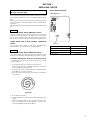
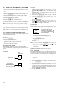
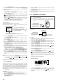
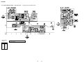
HCD-PX5 is the Amplifier, CD player, MD
Deck and Tuner section in CMT-PX5.
Photo: Silver model
US and foreign patents licensed from Dolby
Laboratories.
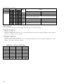
MD
Section
Model Name Using Similar Mechanism
HCD-MD595
MD Mechanism Type
MDM-7X2A
Optical Pick-up Name
KMS-262A/J1N
Model Name Using Similar Mechanism
NEW
CD
CD Mechanism Type
CDM63-21BD53
Section
Base Unit Name
BU-21BD53
Optical Pick-up Name
OP Assy (A-MAX. 2)
SPECIFICATIONS
Amplifier section
MD deck section
Tourist model:
System
Laser
Continuous RMS power output (Reference):
20 + 20 watts (6 ohms at 1 kHz,
10% THD, 240 V)
Laser output
Other models:
Continuous RMS power output (Reference):
20 + 20 watts (6 ohms at 1 kHz,
10% THD, 220 V)
Inputs
TAPE IN (phono jacks): voltage 250 mV, impedance
47 kilohms
DIGITAL OPTICAL IN (Supported sampling frequencies:
32 kHz, 44.1 kHz and 48 kHz)
ANALOG IN (stereo minijack):
voltage 250 mV, impedance
47 kilohms
Outputs
TAPE OUT (phono jacks):voltage 250 mV, impedance
1 kilohm
PHONES (stereo minijack):
accepts headphones of 8 ohms or
more.
SPEAKER:
accepts impedance of 6 to 16
ohms.
Sampling frequency
Frequency response
General
MiniDisc digital audio system
Semiconductor laser (λ=780 nm)
Emission duration: continuous
Max. 44.6 µW*
* This output is the value
measured at a distance of 200 mm
from the objective lens surface on
the Optical Pick-up Block with a
7 mm aperture.
44.1 kHz
5 Hz – 20 kHz
Power requirements
Tourist model:
Other models:
Power consumption
Tourist model:
110 – 120 V or 220 – 240 V
AC, 50/60 Hz
Adjustable with voltage selector
220 V AC, 50/60 Hz
75 watts during normal operation
240 V AC
Other models:
60 watts during normal operation
Dimensions (w/h/d) incl. projecting parts and controls
Approx. 175 × 250 × 370 mm
Mass
Approx. 7.5 kg
Tuner section
FM stereo, FM/AM superheterodyne tuner
FM tuner section
Tuning range
Tourist model:
Other models:
Aerial
Aerial terminals
Intermediate frequency
Design and specifications are subject to change
without notice.
76.0 – 108.0 MHz
(50 kHz step)
87.5 – 108.0 MHz
(50 kHz step)
FM lead aerial
75 ohms unbalanced
10.7 MHz
AM tuner section
Tuning range
CD player section
System
531 – 1,602 kHz
(with the interval set at 9 kHz)
530 – 1,710 kHz
(with the interval set at 10 kHz)
AM loop aerial
External aerial terminals
450 kHz
Frequency response
Compact disc and digital audio
system
Semiconductor laser (λ=800 nm)
Emission duration: continuous
Max. 44.6 µW*
* This output is the value
measured at a distance of 200 mm
from the objective lens surface on
the Optical Pick-up Block with a
7 mm aperture.
2 Hz – 20 kHz
9-929-568-13
Sony Corporation
2002K0500-1
C 2002.11
Home Audio Company
Published by Sony Engineering Corporation
Laser
Laser output
Aerial
Intermediate frequency
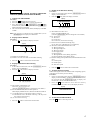
COMPACT DISC DECK RECEIVER
SELF-DIAGNOSIS FUNCTION
The self-diagnosis function consists of error codes for customers, which are displayed automatically when errors occur, and error codes,
which show the error history in the test mode during servicing. For details on how to view error codes for the customer, refer to the
following box in the instruction manual. For details on how to check error codes during servicing, refer to the following “Procedure for
using the Self-Diagnosis Function (Error History Display Mode)”.
Self-diagnosis Display
This system has a Self-diagnosis display function
to let you know if there is a system malfunction.
The display shows a code made up of three or five
letters and a message alternately to show you the
problem. To solve the problem refer to the
following list. If any problem persists, consult
your nearest Sony dealer.
C11/Protected
The MD is protected against erasure.
cRemove the MD and slide the tab to close the
slot.
C12/Cannot Copy
You tried to record a CD or MD with a format
that the system does not support, such as a CDROM.
cRemove the disc and turn off the system once,
then turn it on again.
C13/REC Error
Recording could not be performed properly.
cMove the system to a stable place, and start
recording over from the beginning.
The MD is dirty or scratched, or the MD does
not meet the standards.
cReplace the MD and start recording over from
the beginning.
C13/Read Error
The MD deck cannot read the disc information
properly.
cRemove the MD once, then insert it again.
C14/Toc Error
The MD deck cannot read the disc information
properly.
cReplace the MD.
cErase all the recorded contents of the MD
using the All Erase function.
C41/Cannot Copy
The sound source is a copy of a commercially
available music software, or you tried to record
a CD-R (Recordable CD).
cThe Serial Copy Management System
prevents making a digital copy.
You cannot record a CD-R.
C71/Check OPT-IN
This appears momentarily because of the signal
of the digital broadcast during recording.
cThere is no affect on the recorded contents.
No component is connected to the DIGITAL
OPTICAL IN jack, or a digital component is
not connected properly.
cConnect a digital component to the DIGITAL
OPTICAL IN jack properly using a digital
connecting cable (not supplied).
The connected digital component is not turned
on.
cSee the operating instructions supplied with
the connected component and confirm
whether the component is turned on.
The digital connecting cable connected to the
DIGITAL OPTICAL IN jack is pulled out, or
the connected digital component is turned off
during digital recording.
cConnect the cable, or turn on the digital
component.
E0001/MEMORY NG
There is an error in the internal data that the
system needs in order to operate.
cConsult your nearest Sony dealer.
E0101/LASER NG
There is a problem with the optical pickup.
cThe optical pickup may have failed. Consult
your nearest Sony dealer.
MD SECTION
PROCEDURE FOR USING THE SELF-DIAGNOSIS FUNCTION (ERROR HISTORY DISPLAY MODE)
Note: Perform the self-diagnosis function in the “error history display mode” in the MD test mode. The following describes the least required procedure.
Be careful not to enter other modes by mistake. If you set other modes accidentally, press the [MENU/NO] button to exit the mode.
Procedure:
1. Press the I/1 button to turn the power on.
2. Press the [FUNCTION] button to set the MD function.
3. Press three buttons of x , [MD N X ], Z (CD3) simultaneously to enter the MD test mode and display “[Check]”.
4. Turn the [ENTER/YES] knob to display “[Service]”.
5. Press the [ENTER/YES] button to display “AUTO CHECK” (C01), and turn the [ENTER/YES] knob to display “Err Display” (C02).
6. Press the [ENTER/YES] button to enter the error history mode and display “op rec tm”.
7. Select the contents to be displayed or executed using the [ENTER/YES] knob.
8. Press the [CD SYNC NORM SPEED] button to light up “IT” indicator, then press the [REC MODE] button will display or execute the
contents selected.
9. Press the [REC MODE] button another time returns to step 7.
10. Press the [MENU/NO] button displays “Err Display” (C02) and release the error history mode.
11. To release the MD test mode, press the [REPEAT] button to display “Initialize” and release the MD test mode.
2
ITEMS OF ERROR HISTORY MODE ITEMS AND CONTENTS
Display
Details of History
op rec tm
Cumulative recording time is displayed.
When cumulative recording time is over 1 minute, the hour and minute are displayed as they are.
When it is under 1 minute, “Under 1 min” is displayed.
The displayed time is the total time the laser is set to the high power state.
This is about 1/4 of the actual recording time. The time is displayed in decimal digits.
op play tm
Cumulative playing time is displayed.
When cumulative playing time is over 1 minute, the hour and minute are displayed as they are.
When it is under 1 minute, “Under 1 min” is displayed.
The displayed time is the total of the actual play time. Pauses are not counted.
The time is displayed in decimal digits.
spdl rp tm
Cumulative spindle motor running time is displayed.
When cumulative spindle motor run time is over 1 minute, the hour and minute are displayed as they are.
When it is under 1 minute, “Under 1 min” is displayed.
The time is displayed in decimal digits.
retry err
Displays the total number of retries during recording and number of retry errors during play.
Displayed as “r ss p ss”.
“r” indicates the retries during recording while “p” indicates the retry errors during play.
The number of retries and retry errors are displayed in hexadecimal digits from 00 to FF.
total err
Displays the total number of errors.
Displayed as “total ss”.
The number of errors is displayed in hexadecimal digits from 00 to FF.
err history
Displays the 10 latest errors.
Displayed as “0s ErrCd @@”.
s indicates the history number. The smaller the number, the more recent is the error. (00 is the latest)
@@ indicates the error code.
Refer to the following table for the details. The error history can be switched by turning the [ENTER/YES]
knob.
retry adrs
Display the 5 latest retry address.
Display as “ss ADRS@@@@”.
ss indicates the history number. The smaller the number, the more recent is the error. (00 is the latest)
@@@@ indicates the cluster of retry address.
The number of retry address can be switched by turning the [ENTER/YES] knob.
er refresh
Mode to clear the error history and retry address history.
Procedure:
1) Press the [REC MODE] button.
2) The display will change to “er refresh?”, and then press the [ENTER/YES] button.
The operation is over if “Complete!” is displayed.
After this mode was executed, check the following:
• The data have been cleared.
• Perform the recording and playing to check that the mechanism operates normally.
op change
Mode to clear cumulative time of “op rec tm” and “op play tm”.
These historical data are used to determine the timing when the optical pick-up is to be replaced. When the
optical pick-up was replaced, perform this operation to clear historical data.
Procedure:
1) Press the [REC MODE] button.
2) The display will change to “op change?”, and then press the [ENTER/YES] button.
The operation is over if “Complete!” is displayed.
spdl change
Mode to clear cumulative time of “spdl rp tm”.
This historical data is used to determine the timing when the spindle motor is to be replaced. When the spindle
motor was replaced, perform this operation to clear historical data.
Procedure:
1) Press the [REC MODE] button.
2) The display will change to “spdl change?”, and then press the [ENTER/YES] button.
The operation is over if “Complete!” is displayed.
3
Table of Error Codes
Error Code
4
Details of Error
10
Loading failed
12
Loading switch combination is illegal
20
Head of PTOC could not be read within the
specified time
21
Head of PTOC could be read but its content is
erroneous
22
Access to UTOC could not be made within the
specified time
23
UTOC could be not read within the specified
time
24
Content of UTOC is erroneous
30
Playing could not start
31
Content of sector is erroneous
40
Cause of retry occurred during normal recording
41
D-RAM overflowed and retry was executed
42
Retry was executed during the writing to TOC
43
S.F editing was interrupted by retry
50
Address could not be read except in access
processing
51
Focusing failed and it is out of control
60
Unlock retry
CD SECTION
PROCEDURE FOR USING THE SELF-DIAGNOSIS
FUNCTION (ERROR HISTORY DISPLAY MODE)
1. To Enter The CD Test Mode
Procedure:
1. Press the I/1 button to turn the power on.
2. Press the [FUNCTION] button to set the CD function.
3. Press three buttons of x , [ENTER/YES], and Z (CD2)
simultaneously (When releasing the buttons, the [ENTER/YES]
button is the last to be released).
4. The set enter the CD test mode (menu) and displays “dvt ERR
CODE”.
Note: If the consequence was diaplayed except “dvt ERR CODE”, turn the
[ENTER/YES] knob to display “dvt ERR CODE”.
2. Display of Error Number
Procedure:
1. Press the Z (CD1) button to display as bellow.
Display
Emc=**Edc=**
(a)
(b)
(a) Number of mechanical error.
(b) Number of no disc error that occurred after chucking.
2. Press the x button to release the CD test mode.
3. Display of Mechanical Error History
Procedure:
1. In the CD test mode menu, turn the [ENTER/YES] knob to
display “dvt ECODE MEC”.
2. Press the Z (CD1) button to display as bellow.
Display
E**M********00
(a)
(b) (c) (d) (e)
(a) The number of mechanical error.
Latest one “00” to last ten “09”
(Turn the [ENTER/YES] knob to change the error number)
(b) FF: Mechanical error, when normal operation.
Other display: Mechanical error, between mechanical initialize.
(c) 7x: Mechanical error in the midst of select a sub tray.
9x: Mechanical error in the midst of moving a sub tray from
the stocker to the main tray.
(d), (e): Not used in servicing.
4. Display of No Disc Error History
Procedure:
1. In the CD test mode menu, turn the [ENTER/YES] knob to
display “dvt ECODE BU”.
2. Press the Z (CD1) button to display as bellow.
Display
E**D********
(a)
(b) (c) (d) (e)
(a) The number of no disc error.
Latest one “00” to last ten “09”
(Turn the [ENTER/YES] knob to change the error number)
(b) 01: Focus error
02: GFS error
03: Set up error
04: Focus error (not used in servicing)
(c) 00:No disc error (Did not chucking retry)
02: No disc error (Chucking retry to completion)
(d) The status, when determined no disc error.
2x: During setting up
3x: During reading TOC
4x: During accessing
5x: During playback
6x: During pause
7x: During manual search (during playback)
8x: During manual search (during pause)
(e) Rotation setting of the spindle motor, when determined no disc
error.
01: normal speed
02: double speed
04: four times speed
3. Press the x button to release the CD test mode.
4. To Erase The Error History
When returning the unit to the customer after completing repairs,
perform this to erase the past error history.
Procedure:
1. In the CD test mode menu, turn the [ENTER/YES] knob to
display “dvt ECNT0 MEC”. (When erase the mechanical error)
Or one more turn the [ENTER/YES] knob to display “dvt
ECNT0 BU”. (When erase the no disc error)
2. Press the Z (CD1) button to erase the error history
(mechanical error or no disc error) and display as bellow.
Display
Emc=00Edc=00
5. To Release The CD Test Mode
Press the I/1 button to turn the power off.
3. Press the x button to release the CD test mode.
5
TABLE OF CONTENTS
SELF-DIAGNOSIS FUNCTION ....................................
2
1.
SERVICING NOTES ..............................................
7
2.
GENERAL .................................................................. 16
3.
DISASSEMBLY ........................................................ 19
4.
TEST MODE .............................................................. 32
5.
ELECTRICAL ADJUSTMENTS
MD Section .................................................................... 37
CD Section ..................................................................... 47
6.
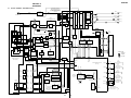
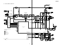
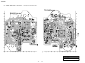
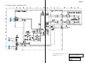
DIAGRAMS
6-1.
6-2.
6-3.
6-4.
6-5.
6-31.
Block Diagram – MD SERVO Section – ......................
Block Diagram – D/A, A/D CONVERTER Section – ..
Block Diagram – MAIN Section ...................................
Block Diagram – DISPLAY/POWER Section – ...........
Note for Printed Wiring Boards and
Schematic Diagrams ......................................................
Printed Wiring Board – BD (CD) Board – ....................
Schematic Diagram – BD (CD) Board – .......................
Printed Wiring Boards – CD CHANGER Section – .....
Schematic Diagram – CD CHANGER Section – .........
Schematic Diagram – BD (MD) Board (1/2) – .............
Schematic Diagram – BD (MD) Board (2/2) – .............
Printed Wiring Boards – BD (MD) Board – ..................
Schematic Diagram – MD DIGITAL Board (1/3) – .....
Schematic Diagram
– MD DIGITAL (2/3)/RELAY Boards – .......................
Schematic Diagram – MD DIGITAL Board (3/3) – .....
Printed Wiring Board
– MD DIGITAL Board (Component Side) – ................
Printed Wiring Boards
– MD DIGITAL (Conductor Side)/RELAY Boards – ..
Schematic Diagram – MAIN Board (1/2) – ..................
Schematic Diagram – MAIN Board (2/2) – ..................
Printed Wiring Board – MAIN Board – .......................
Printed Wiring Board – AMP Board – ..........................
Schematic Diagram – AMP Board – .............................
Printed Wiring Boards – JACK/JOG Boards – ..............
Schematic Diagram – JACK/JOG Boards – ..................
Schematic Diagram – PANEL Board – ........................
Printed Wiring Board – PANEL Board – ......................
Printed Wiring Board – REG Board – ...........................
Schematic Diagram – REG Board – ..............................
Printed Wiring Boards
– POWER/SELECTOR Boards – ..................................
Schematic Diagram
– POWER/SELECTOR Boards – ..................................
IC Pin Function Description ..........................................
7.
EXPLODED VIEWS ............................................... 95
8.
ELECTRICAL PARTS LIST .............................. 102
6-6.
6-7.
6-8.
6-9.
6-10.
6-11.
6-12.
6-13.
6-14.
6-15.
6-16.
6-17.
6-18.
6-19.
6-20.
6-21.
6-22.
6-23.
6-24.
6-25.
6-26.
6-27.
6-28.
6-29.
6-30.
6
49
50
51
52
Notes on chip component replacement
• Never reuse a disconnected chip component.
• Notice that the minus side of a tantalum capacitor may be damaged by heat.
Flexible Circuit Board Repairing
• Keep the temperature of the soldering iron around 270 ˚C during repairing.
• Do not touch the soldering iron on the same conductor of the
circuit board (within 3 times).
• Be careful not to apply force on the conductor when soldering
or unsoldering.
CAUTION
Use of controls or adjustments or performance of procedures
other than those specified herein may result in hazardous radiation exposure.
53
54
55
56
57
58
59
60
61
This appliance is classified as a CLASS 1 LASER product.
The CLASS 1 LASER PRODUCT MARKING is located on
the rear exterior.
62
63
Laser component in this product is capable of emitting radiation
exceeding the limit for Class 1.
64
65
66
67
68
70
71
72
73
74
75
76
77
78
79
83
SAFETY-RELATED COMPONENT WARNING!!
COMPONENTS IDENTIFIED BY MARK 0 OR DOTTED
LINE WITH MARK 0 ON THE SCHEMATIC DIAGRAMS
AND IN THE PARTS LIST ARE CRITICAL TO SAFE
OPERATION. REPLACE THESE COMPONENTS WITH
SONY PARTS WHOSE PART NUMBERS APPEAR AS
SHOWN IN THIS MANUAL OR IN SUPPLEMENTS PUBLISHED BY SONY.
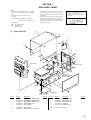
SECTION 1
SERVICING NOTES
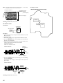
NOTES ON HANDLING THE OPTICAL PICK-UP
BLOCK OR BASE UNIT
MODEL IDENTIFICATION
— Back panel —
The laser diode in the optical pick-up block may suffer electrostatic break-down because of the potential difference generated
by the charged electrostatic load, etc. on clothing and the human
body.
During repair, pay attention to electrostatic break-down and also
use the procedure in the printed matter which is included in the
repair parts.
The flexible board is easily damaged and should be handled with
care.
For CD
NOTES ON LASER DIODE EMISSION CHECK
The laser beam on this model is concentrated so as to be focused
on the disc reflective surface by the objective lens in the optical
pick-up block. Therefore, when checking the laser diode emission, observe from more than 30 cm away from the objective lens.
LASER DIODE AND FOCUS SEARCH OPERATION
CHECK
Carry out the “S curve check” in “CD section adjustment” and
check that the S curve waveforms is output three times.
PART No.
Model
For MD
NOTES ON LASER DIODE EMISSION CHECK
Never look into the laser diode emission from right above when
checking it for adjustment. It is feared that you will lose your sight.
Part No.
Korean model
4-229-859-4[]
4-229-859-5[]
Tourist model
4-229-859-6[]
Hong Kong model
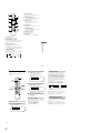
CLEANING OBJECTIVE LENS OF OPTICAL PICK-UP
• In cleaning the objective lens of optical pick-up, be sure the
following below.
1. In cleaning the lens, do not apply an excessive force.
As the optical pick-up is vulnerable, application of excessive
force could damage the lens holder.
2. In cleaning, do not use a cleaner other than exclusive cleaning
liquid (KK-91 or isopropyl alcohol).
3. Wipe the objective lens spirally from center toward outside.
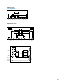
(See Figure A)
(Figure A)
4. Eject the disk, if loaded.
5. Disconnect the power cord from the socket to shut off the power
supply.
6. When cleaning the objective lens of optical pick-up in CD,
refer to “CD BASE UNIT (BU-21BD53)” on page 26 for
removing CD BASE UNIT (BU-21BD53).
7
MC COLD RESET
• The cold reset clears all data including preset data stored in the RAM to initial conditions. Execute this mode when returning the set to
the customer.
Procedure:
1. Press the I/1 button to turn the power on.
2. Press three buttons of x , [CLEAR] and [FUNCTION] simultaneously.
3. The set is reset, and displays “COLD RESET”, then becomes standby status.
AMP TEST
Procedure:
1. Press the I/1 button to turn the power on.
2. Press three buttons of x , [TUNER/BAND], and Z (CD1) simultaneously.
3. Each buttons are pressed, it changes display as follows.
Button
Display
x
7[TESTMIN]
REC MODE
8[TESTMID]
ENTER/YES
9[TESTMAX]
MD Z
10[TESTSUR]
4. [VOLUME] knob is turned, it changes display as follows.
Turn Direction
Display
counterclockwise
VOLUME MIN
center
VOLUME 21
clockwise
VOLUME MAX
5. To release from this mode, press the I/1 button to turn the power off and cold reset.
VERSION DISPLAY
Procedure:
1. Press the I/1 button to turn the power on.
2. Press three buttons of x , [TUNER/BAND] and [REPEAT] simultaneously.
3. Enter the version display mode and display STR version.
4. Each time the [ENTER/YES] button is pressed, it changes display STR version → CD version → MD version → STR version → ...
5. To release from this mode, press the I/1 button to turn the power off.
LCD AND LED TEST
Procedure:
1. Press the I/1 button to turn the power on.
2. Press three buttons of x , [TUNER/BAND] and [CD2] simultaneously.
3. Liquid crystal display and LEDs are all turned on.
4. Each time the [ENTER/YES] button is pressed, it changes display all turned on → all goes off → pattern 1 → pattern 2 → all turned
on → ...
5. Each time the x button is pressed, it changes LED indication all turned on → all goes off → turn on the green LEDs (*1) → turn on the
amber LEDs (*1) → all turned on → ...
*1) The color changable LEDs are “CD N X”, “MD N X”, “CD1”, “CD2” and “CD3”.
6. To release from this mode, press the I/1 button to turn the power off.
KEY TEST
Procedure:
1. Press the I/1 button to turn the power on.
2. Press three buttons of x , [TUNER/BAND] and [CD1] simultaneously.
3. Enter the key test mode and display “KEY00 JOG0VOL0”.
4. Each time a button (including m and M of [CURSOR] knob) is pressed, “KEY” value increases. However, once a button is
pressed, it is no longer taken into account.
“JOG” value increases like 0, 1, 2 ... if turn the [ENTER/YES] knob clockwise, or it decreases like 9, 8, 7 ... if turn the [ENTER/YES]
knob counterclockwise.
“VOL” value increases like 0, 1, 2 ... if turn the [VOLUME] knob clockwise, or it decreases like 9, 8, 7 ... if turn the [VOLUME] knob
counterclockwise.
5. To release from this mode, press three buttons in the same manner as step 2 , or disconnect the power cord.
8
MD SECTION
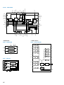
JIG FOR CHECKING BD (MD) BOARD WAVEFORM
The special jig (J-2501-196-A) is useful for checking the waveform of the BD (MD) board. The names of terminals and the checking items
to be performed are shown as follows.
I+3V
IOP
GND
TE
FE
VC
RF
: For measuring IOP (Check the deterioration of the optical pick-up laser)
: For measuring IOP (Check the deterioration of the optical pick-up laser)
: Ground
: Tracking error signal (Traverse adjustment)
: Focus error signal
: Reference level for checking the signal
: RF signal (Check jitter)
CN105
IOP
TE
I+3V
GND
FE
VC
RF
1
I+3V
IOP
GND
TE
FE
VC
RF
I+3V
IOP
GND
TE
FE
VC
RF
for
MDM-7X2A
7
9
IOP DATA RECORDING AND DISPLAY WHEN OPTICAL PICK-UP AND NON-VOLATILE MEMORY (IC195 OF BD
(MD) BOARD) ARE REPLACED
The IOP value labeled on the optical pick-up can be recorded in the non-volatile memory. By recording the value, it will eliminate the need
to look at the value on the label of the optical pick-up. When replacing the optical pick-up or non-volatile memory (IC195 of BD (MD)
board), record the IOP value on the optical pick-up according to the following procedure.
Record Procedure:
1. Press the I/1 button to turn the power on.
2. Press the [FUNCTION] button to set the MD function.
3. Press three buttons of x , [MD N X ] and Z (CD3) simultaneously to enter the MD test mode and display “[Check]”.
4. Turn the [ENTER/YES] knob to display “[Service]”.
5. Press the [ENTER/YES] button to display “AUTO CHECK” (C01), and turn the [ENTER/YES] knob to display “Iop Write” (C05).
6. Press the [ENTER/YES] button.
7. The display becomes “Ref= @@@.@” (@ is an arbitrary number) and the numbers which can be changed will blink.
8. Input the IOP value written on the optical pick-up.
To select the number : Turn the [ENTER/YES] knob.
To select the digit
: After press the [CD SYNC NORM SPEED] button to lights up the “IT” indication, press the [REC MODE]
button.
9. When the [ENTER/YES] button is pressed, the display becomes “Measu=@@@.@” (@ is an arbitrary number).
10. As the adjustment results are recorded for the step 8 value. Leave it as it is and press the [ENTER/YES] button.
11. “Complete!” will be displayed momentarily. The value will be recorded in the non-volatile memory and the display will become “Iop
Write” (C05).
12. Press the [REPEAT] button to complete. “Initialize” will be displayed and release the MD test mode.
Display Precedure:
1. Press the I/1 button to turn the power on.
2. Press the [FUNCTION] button to set the MD function.
3. Press three buttons of x , [MD N X ] and Z (CD3) simultaneously to enter the MD test mode and display “[Check]”.
4. Turn the [ENTER/YES] knob to display “[Service]”.
5. Press the [ENTER/YES] button to display “AUTO CHECK” (C01), and turn the [ENTER/YES] knob to display “Iop Read” (C26).
6. Press the [ENTER/YES] button.
7. “@@.@/##.#” is displayed and the recorded contents are displayed.
@@.@ : Indicates the Iop value labeled on the pick-up.
##.#
: Indicates the Iop value after adjustment.
8. Press the [REPEAT] button to complete. “Initialize” will be displayed and release the MD test mode.
WHEN MEMORY NG IS DISPLAYED
If the nonvolatile memory data is abnormal, “E001 MEMORY NG” will be displayed so that the MD deck does not continue operations.
In this case, set the test mode promptly and perform the following procedure.
Procedure:
1. Enter the MD test mode (refer to page 32).
2. Normally a message for selecting the test mode will be displayed. However if the nonvolatile memory is abnormal, the following will be
displayed “INIT EEP?”.
3. Press three buttons of x , [MD N X ] and [REC MODE] simultaneously.
4. Turn the [ENTER/YES] knob to display “MDM-7X2A”.
5. After press the [CD SYNC NORM SPEED] button to lights up the “IT” indication, press the [REC MODE] button. If the nonvolatile
memory is successfully overwritten, the normal MD test mode will be set and a message to select the MD test mode will be displayed.
10
RETRY CAUSE DISPLAY MODE IN MD
• In this test mode, the causes for retry of the unit during recording can be displayed on the liquid crystal display. During playback, the
“track mode” for obtaining track information will be set.
This is useful for locating the faulty part of the unit.
• The following will be displayed :
During recording and stop : Retry cause, number of retries, and number of retry errors.
During playback
: Information such as type of disc played, part played, copyright.
These are displayed in hexadecimal.
Precedure:
1. Load a recordable disc whose contents can be erased into the unit.
2. Press the [MENU/NO] button. When “Edit Menu” is displayed on the liquid crystal display, turn the [ENTER/YES] knob to
display “All Erase?”.
3. Press the [ENTER/YES] button.
4. “All Erase??” is displayed on the liquid crystal display.
5. Press the [ENTER/YES] button to display “Complete!”.
6. Press the [REC/REC IT] button to start recording. Then press the [MD N X] button and start recording. If recording cannot be performed,
press the [FUNCTION] button and set a different function.
7. Press three buttons of x , [MD N X ] and [CD1] simultaneously to enter the retry cause display mode.
8. To check the “track mode”, press the [MD N X ] button to start playback.
9. To release this mode, press the I/1 button to turn the power off. When “TOC” goes off, disconnect the power plug from the outlet.
If the test mode cannot be released, refer to “MC COLD RESET” on page 8.
Fig. 1 Reading the Test Mode Display
(During recording and stop)
Fig. 2 Reading the Test Mode Display
(During playback)
RTs@@c##e**
Liquid crystal display
@@ ###** $$
Liquid crystal display
@@ :
## :
** :
$$ :
@@ : Cause of retry
## : Number of retries
** : Number of retry errors
Parts No. (name of area named on TOC)
Cluster
Sector Address
Track mode (Track information such as copyright information of each part)
Reading the Retry Cause Display
Higher Bits
Hexa1 decimal
b7 b6 b5 b4 b3 b2 b1 b0
Hexadecimal 8
Bit
Binary
Lower Bits
Occurring conditions
Cause of Retry
4
2
1
8
4
2
0
0
0
0
0
0
0
1
01
shock
When track jump (shock) is detected
0
0
0
0
0
0
1
0
02
ader5
When ADER was counted more than five times
continuously
0
0
0
0
0
1
0
0
04
0
0
0
0
1
0
0
0
08
Discontinuous address When ADIP address is not continuous
When DIN unlock is detected
DIN unlock
0
0
0
1
0
0
0
0
10
FCS incorrect
When not in focus
0
0
1
0
0
0
0
0
20
IVR rec error
When ABCD signal level exceeds the specified range
0
1
0
0
0
0
0
0
40
CLV unlock
When CLV is unlocked
1
0
0
0
0
0
0
0
80
Access fault
When access operation is not performed normally
Reading the Display:
Convert the hexadecimal display into binary display. If more than two causes, they will be added.
Example
When 42 is displayed:
Higher bit: 4 = 0100 t b6
Lower bit : 2 = 0010 t b1
In this case, the retry cause is combined of “CLV unlock” and “ader5”.
When A2 is displayed:
Higher bit: A = 1010 t b7 + b5
Lower bit : 2 = 0010 t b1
The retry cause in this case is combined of “Access fault”, “IVR rec error”, and “ader5”.
11
Reading the Retry Cause Display
Higher Bits Lower Bits
HexaHexadecimal 8 4 2 1 8 4 2 1 decimal
Bit
b7 b6 b5 b4 b3 b2 b1 b0
Binary
Details
When 1
When 0
0
0
0
0
0
0
0
1
01
Emphasis OFF
Emphasis ON
0
0
0
0
0
0
1
0
02
Monaural
Stereo
0
0
0
0
0
1
0
0
04
0
0
0
0
1
0
0
0
08
This is 2-bit display. Normally 01.
01: Normal audio. Others: Invalid
0
0
0
1
0
0
0
0
10
Audio (Normal)
Invalid
0
0
1
0
0
0
0
0
20
Original
Digital copy
0
1
0
0
0
0
0
0
40
Copyright
No copyright
1
0
0
0
0
0
0
0
80
Write prohibited
Write allowed
Reading the Display:
Convert the hexadecimal display into binary display. If more than two causes, they will be added.
Example When 84 is displayed:
Higher bit : 8 = 1000 t b7
Lower bit : 4 = 0100 t b2
In this case, as b2 and b7 are 1 and others are 0, it can be determined that the retry cause is combined of “Emphasis OFF”, “Monaural”,
“Original”, “Copyright”, and “Write allowed”.
Example When 07 is displayed:
Higher bit : 0 = 0000 t All 0
Lower bit : 7 = 0111 t b0 + b1 + b2
In this case, as b0, b1, and b2 are 1 and others are 0, it can be determined that the retry cause is combined of “Emphasis ON”, “Stereo”,
“Original”, “Copyright”, and “Write prohibited”.
Hexadecimal t Binary Conversion Table
Hexadecimal
Binary
Hexadecimal
Binary
0
0000
8
1000
1
0001
9
1001
2
0010
A
1010
3
0011
B
1011
4
0100
C
1100
5
0101
D
1101
6
0110
E
1110
7
0111
F
1111
12
CD SECTION
CD AGING MODE
Procedure:
1. Press the I/1 button to turn the power on.
2. Press the [FUNCTION] button to set the CD function, insert a disc to the each disc tray (CD1 to 3).
3. Press three buttons of x , [ENTER/YES] and [CD3] simultaneously (When releasing the buttons, the [ENTER/YES] button is the
last to be released).
4. The set displays “AGING SEL=00”. Between it is displayed, press the Z (CD1) button to start CD aging mode.
5. The sequence during the CD aging mode is following as below.
CD aging mode sequence:
CD1 disc tray open
CD1 disc tray close
CD1 TOC read
Playback CD1 track 1
Playback CD1 last track
CD2 disc tray open
CD2 disc tray close
CD2 TOC read
Playback CD2 track 1
Playback CD2 last track
CD3 disc tray open
CD3 disc tray close
CD3 TOC read
Playback CD3 track 1
Playback CD3 last track
Display aging number
6. To release from this mode, press the I/1 button to turn the power off.
Note: Refer to “Error History Display Mode” (page 5) for display at an error occurred.
13
CD-TEXT TEST DISC
This unit is able to display the test data (character information) written in the CD on its fluorescent indicator tube.
The CD-TEXT TEST DISC (TGCS-313:4-989-366-01) is used for checking the display.
To check, perform the following procedure.
Checking Method:
1. Press the I/1 button to turn the power on, set the disc to the disc table with the “test disc” label facing up, and chuck the disc.
2. Press the [CD N X ] button and playback the disc.
3. The following will be displayed on the liquid crystal display.
Display : 1kHz/0db/L&R
4. Pressing the . m or M > button, select the track. The text data of each track will be displayed.
For details of the displayed contents for each track, refer to “Table 1 : CD-TEXT TEST DISC TEXT Data Contents” and “Table 2 : CDTEXT TEST DISC Recorded Contents and Display”.
Restrictions in CD-TEXT Display
In this unit, some special characters will not be displayed properly. These will be displayed as a space or a character resembling it. For
details, refer to “Table 2 : CD-TEXT DISC Recorded Contents and Display”.
Table 1 : CD-TEXT TEST DISC TEXT Data Contents (TRACKS No. 1 to 41:Normal Characters)
TRACK
No.
Displayed Contents
TRACK
Displayed Contents
No.
1
1kHz/0dB/L&R
22
1kHz/–90dB/L&R
2
20Hz/0dB/L&R
23
Infinity Zero w/o emphasis//L&R
3
40Hz/0dB/L&R
24
Infinity Zero with emphasis//L&R
4
100Hz/0dB/L&R
25
400Hz+7kHz(4:1)/0dB/L&R
5
200Hz/0dB/L&R
26
400Hz+7kHz(4:1)/–10dB/L&R
6
500Hz/0dB/L&R
27
19kHz+20kHz(1:1)/0dB/L&R
7
1kHz/0dB/L&R
28
19kHz+20kHz(1:1)/–10dB/L&R
8
5kHz/0dB/L&R
29
100Hz/0dB/L*
9
7kHz/0dB/L&R
30
1kHz/0dB/L*
10
10kHz/0dB/L&R
31
10kHz/0dB/L*
11
16kHz/0dB/L&R
32
20kHz/0dB/L*
12
18kHz/0dB/L&R
33
100Hz/0dB/R*
13
20kHz/0dB/L&R
34
1kHz/0dB/R*
14
1kHz/0dB/L&R
35
10kHz/0dB/R*
15
1kHz/–1dB/L&R
36
20kHz/0dB/R*
16
1kHz/–3dB/L&R
37
100Hz Squer Wave//L&R
17
1kHz/–6dB/L&R
38
1kHz Squer Wave//L&R
18
1kHz/–10dB/L&R
39
1kHz w/emphasis/–0.37dB/L&R
19
1kHz/–20dB/L&R
40
5kHz w/emphasis/–4.53dB/L&R
20
1kHz/–60dB/L&R
41
16kHz w/emphasis/–9.04dB/L&R
21
1kHz/–80dB/L&R
Note: The contents of Track No. 1 to 41 are the same as those of the current TEST DISC-their titles are displayed.
14
Table 2: CD-TEXT TEST DISC Recorded Contents and Display
(In this unit, some special characters cannot be displayed. This is not a fault)
TRACK
No.
Recorded contents
Display
42
! ” # $ %& ´
(21h to 27h)1kHz 0dB L&R
T All the same
43
( )
+ , – . /
(28h to 2Fh)
T All the same
44
012345 67
(30h to 37h)
T All the same
45
89 : ; <=>?
(38h to 3Fh)
T All the same
46
@A B C D E F G
(40h to 47h)
T All the same
47
H I J K L MNO
(48h to 4Fh)
T All the same
48
P Q R S T U V W (50h to 57h)
T All the same
49
XYZ [ ¥ ] ^ _
(58h to 5Fh)
XYZ [ \ ] ^ _
50
′
ab c de f g
(60h to 67h)
T All the same
51
h i j k l mn o
(68h to 6Fh)
T All the same
52
pq r s t u vw
(70h to 77h)
T All the same
53
x y z { I } ~
(78h to 7Fh)
T All the same
*
i ¢£¤¥ §
C ª ¬ PR–
54
(A0h to A7h) 8859-1
(A0h to A7h) 8859-1
(A8h to AFh)
(A8h to AFh)
′
µ¶ •
(B0h to B7h)
(B0h to B7h)
1
4
1
2
¿
(B8h to BFh)
À Á Â Ã Ä Å ÆÇ
(C0h to C7h)
55
•
±
57
†
1
58
59
È ÉÊË Ì Í Î Ï
60
61
D ÑÒÓÔÕÖ
Ø Ù Ú Û Ü Y˙ ß
62
63
56
(58h to 5Fh)
2
º
3
3
4
(B8h to BFh)
C
(C0h to C7h)
(C8h to CFh)
EEEE I I I I
(C8h to CFh)
(D0h to D7h)
D NOOOOO
(D0h to D7h)
(D8h to DFh)
OUUUUY
(D8h to DFh)
à á â ã ä åæç
(E0h to E7h)
aaaaaa
c
(E0h to E7h)
è éêë ì í î ï
(E8h to FFh)
eeee i i i i
(E8h to EFh)
64
∂ ñòóôõ ö÷
(F0h to F7h)
dnooooo
(F0h to F7h)
65
ø ù ú û ü y´
(F8h to FFh)
ouuuu y
66
No.66
T All the same
67
No.67
T All the same
to
99
to
No.99
ÿ
AAAAAA
y
(F8h to FFh)
to
T All the same
15
SECTION 2
GENERAL
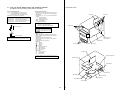
LOCATION OF CONTROLS
• Front View
1 I/1 button and indicator
2 Liquid crystal display
3 VOLUME knob
4 MD disc slot
5 Lid
6 CD disc tray
7 Remote sensor
8 CD N X button and indicator
9 MD N X button and indicator
0 TUNER/BAND button and indicator
qa x button
qs MENU/NO button and indicator
qd ENTER/YES, PUSH knob and button
qf CLEAR button
qg CD1 to 3 buttons and indicators,
Z (CD1 to 3) buttons
qh MD Z button
qj CURSOR m ? M knob
qk PLAY MODE, TUNING MODE button
ql FUNCTION button
w; SYNC MODE, REC MODE button
wa CD SYNC HIGH SPEED button and indicator,
CD SYNC NORM SPEED button
ws REC/REC IT button and indicator
wd PC LINK/KEY BOARD jack
wf PHONES jack
wg ANALOG IN jack
16
• Rear View
1 PC LINK jack
2 SPEAKER terminals
3 DIGITAL OPTICAL IN terminal
4 TAPE IN/OUT jacks
5 FM ANTENNA jack
6 AM ANTENNA terminals
7 AC power cord
Parts descriptions for
the remote
You can use the supplied remote to control the
system.
Note
You cannot perform the following operations with the
remote;
Removing discs
Selecting the recording mode
CD-MD Synchro Recording
1
2
3
6
Parts descriptions for the
remote (continued)
1 ?/1 (power) switch
2 CLOCK/TIMER SELECT button
Press to check timer settings, or to set the timer
on/off. (pages 58, 59)
6 PLAY MODE/TUNING MODE button
This functions as the PLAY MODE button when
playing a CD or MD. Press to select normal play,
Shuffle Play or Programme Play. (pages 9, 16,
17, 22, 23)
Each time you press the button, the display
changes as follows.
CLOCK/TIMER SET button
Press to set the clock and timer functions. (pages
6, 57, 58)
3 TIME button
Press to switch the contents appearing on the
lower level of the display (CD/MD play time
mode, etc.). (pages 7, 19, 24)
During play (CD only):
1DISC y ALL DISCS
DISPLAY button
In stop mode (CD):
Press to switch the contents appearing on the
upper level of the display (preset equalizer name,
clock, disc name/track name/radio station name,
volume, etc.). (pages 7, 19, 24)
t ALL DISCS t 1DISC t ALL DISCS SHUFFLE
PROGRAM T
1DISC SHUFFLE T
In stop mode (MD):
4 MD H (play) button
t No display t SHUFFLE
CD H (play) button
PROGRAM T
This functions as the TUNING MODE button
when listening to the radio. Press to select
MANUAL, AUTO or PRESET tuning.
X (pause) button
7
x (stop) button
D.SKIP button
5 MD z REC button
Press to record. This button is also used to mark a
track number manually during recording. (pages
36, 37)
continued
—/+, ./> (AMS: Automatic Music
Sensor) buttons
Press to skip to the beginning of the next track or
the previous track when playing a CD or MD.
Press to tune the frequency when listening to the
radio.
These buttons are also used to set the clock, make
the Programme Play setting, adjust the recording
level, and select characters to be entered, etc.
ENTER/YES button
Press to set the clock, Programme Play and to
label a CD, MD and preset station, or to enter the
settings in Edit Menu or Setup Menu .
MENU/NO button
Press to label a CD, MD and preset station.
8 TIME MACHINE REC button (page 34)
REPEAT button
Press to select the CD you want to play, record or
edit.
8
buttons
The m/M buttons locate a desired point in a
track during MD play or pause, or during CD
play or pause.
Press to label a CD, MD and preset station, or to
set the clock. (pages 6, 20, 41, 55)
Press to play a track or all the tracks repeatedly.
(pages 16, 22)
Additional Information
4
5
7 TCURSOR/CURSORt, m/M
73
74
17
qd PRESET EQ button
9
Press to select the type of the preset equalizer.
(page 54)
qf
qf STEREO/MONO button
qg
0
Press to switch between stereo and monaural
when receiving a stereo broadcast.
qg SCROLL button
qa
Press to display the disc title or track title
scrolling. (pages 19, 21, 25, 42)
qh
qh CLEAR button
Press to cancel the selection. (pages 18, 21, 23,
42, 56)
qj
qs
qj TUNER/BAND button
qk
Press to select the tuner for the sound source, or
to select the FM or AM band.
qd
ql
qk VOLUME +/— buttons
Press to adjust the volume.
ql DBFB button
Press to reinforce the bass sound. (page 54)
9 SLEEP button
Press to set Sleep Timer. (page 56)
0 NAME EDIT/SELECT button
Additional Information
Press to display the text input screen and to select
the type of characters to be input. (pages 20, 41,
55)
qa Letter/Number buttons
Press to select track numbers of a CD, MD, or
preset station.
Press to enter the corresponding letter or number
at the character input screen. (pages 20, 41, 55)
qs FUNCTION button
Press to switch the sound source.
Each time you press this button, the sound source
changes as follows;
t CD
t TUNER t OPTICAL IN
TAPE T
MD T
ANALOG IN T
75
Step 2: Setting the time
3
Press — or + to set the day, then press
ENTER/YES or CURSORt.
The hour indication flashes.
(Noon is indicated as 12:00 PM, and
midnight as 12:00 AM.)
You must set the time beforehand to use the timer
functions.
1
2
DISPLAY
4
3,4,5
TCURSOR
CURSORt
3,4,5
3,4,5
Press — or + to set the hour, then press
ENTER/YES or CURSORt.
Showing the time
In consideration of reducing standby power, this
system can select whether or not to display the
clock in standby mode. The system is set at the
factory to not display the clock when the system is
off (Power Saving Mode). To display the clock
even when the system is off, press DISPLAY or
TIME while the system is off. Press the button
again to turn the clock display off and activate the
Power Saving Mode.
While the system is on, the information that
appears at the upper level of the display changes
as follows each time you press DISPLAY.
t Preset Equalizer name t Clock
The minute indication flashes.
Name* T
Volume T
* Displayed only when disc title, track title, radio
station name or other name information is labelled.
Nothing appears when this information is not
labelled.
Tip
5
Press — or + to set the minute, then press
ENTER/YES.
The upper dot of the clock display flashes for the first
half of a minute (0 to 29 seconds), and the lower dot
flashes for the last half of a minute (30 to
59 seconds).
The clock starts.
Changing the preset time
If you made a mistake
6
18
1
Turn on the system.
Press TCURSOR or CURSORt until the
indication you wish to change (day, hour, minute)
flashes, then change the setting.
2
Press CLOCK/TIMER SET.
To cancel setting the time
The time setting display appears, and the day
indication SUN flashes.
Press CLOCK/TIMER SET.
1 Press CLOCK/TIMER SET, then press — or +
until CLOCK SET? appears. Press ENTER/
YES.
2 Repeat steps 3 to 5 of Setting the time .
You can change the preset time while the system
is off. In this case, perform steps 2 to 5 of Setting
the time .
SECTION 3
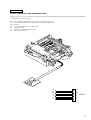
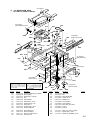
DISASSEMBLY
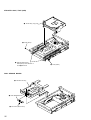
• This set can be disassembled in the order shown below.
SET
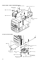
CD BASE UNIT
(BU-21BD53)
(Page 26)
CASE
(Page 20)
BACK PANEL,
DC FAN (M801)
(Page 20)
MAIN BOARD,
TUNER
(Page 21)
PANEL ASSY
(Page 21)
PANEL BOARD
(Page 22)
REG BOARD, AMP BOARD,
HEAT SINK
(Page 25)
POWER BOARD,
POWER TRANSFORMER
(T901)
(Page 26)
MD DIGITAL BOARD,
MD MECHANISM DECK
(MDM-7X2A)
(Page 22)
CD MECHANISM DECK
(CDM63-21BD53)
(Page 27)
BD (MD) BOARD
(Page 23)
FITTING BASE
(STABILIZER) ASSY,
TRAY ASSY, TRAY (SUB)
(Page 28)
HOLDER ASSY
(Page 23)
SLIDER (LOADING),
GEAR (SLIDER)
(Page 29)
TRAY SENSOR BOARD
(Page 29)
GUIDE (L), SLIDER (EJ),
SLIDER, LEVER (HEAD)
(Page 24)
STOCKER ASSY,
TRAY (SUB)
(Page 30)
MOTOR ASSY (M721),
MOTOR BOARD
(Page 31)
OPTICAL PICK-UP
(KMS-262A/J1N),
OVER WRITE HEAD (HR901)
(Page 24)
DISC SENSOR BOARD
(Page 30)
RELAY BOARD
(Page 27)
DRIVER BOARD
(Page 28)
IN OUT SW BOARD
(Page 31)
SPINDLE MOTOR ASSY
(M101),
SLED MOTOR ASSY
(M102),
LOADING MOTOR ASSY
(M103)
(Page 25)
19
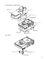
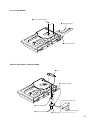
Note: Follow the disassembly procedure in the numerical order given.
CASE
2 three screws (BVTP3 × 12)
4 case
1 three screws
(CASE3 TP2)
3
3
1 three screws
(CASE3 TP2)
BACK PANEL, DC FAN (M801)
9 back panel
3 screw (BVTT3 × 6)
6 DC fan (M801)
5 four screws
(BVTP3 × 20)
2 two screws
(BVTP3 × 10)
3 screw (BVTT3 × 6)
1 connector
(CN851)
3 two screws (BVTP3 × 10)
(Tourist model)
2 four screws
(BVTP3 × 10)
4
3 four screws
(BVTT3 × 6)
7 connector (CN993)
(Tourist model)
8 SELECTOR board
(Tourist model)
20
7 connector (CN994)
(Tourist model)
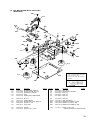
MAIN BOARD, TUNER
7 connector
(CN801)
7 two connectors
(CN803, 852)
7 two connectors
(CN907, 908)
qa harness
7 connector
(CN901)
q; screw (BVTT3 × 6)
8 screw (BVTT3 × 6)
5 wire (flat type) (15 core)
(CN503)
9 tuner
2 connector
(CN505)
1 wire (flat type)
(23 core)
(CN508)
4
qs tape
qd lead
qf MAIN board
5 wire (flat type) (31 core)
(CN506)
6 connector (CN504)
3 two screws (BVTP3 × 8)
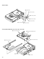
PANEL ASSY
3 panel assy
1 three screws (BVTT3 × 6)
2 two claws
21
PANEL BOARD
5 PANEL board
4 six screws
(BVTP2.6 × 8)
4 four screws (BVTP2.6 × 8)
4 three screws (BVTP2.6 × 8)
6 screw
(BVTP2.6 × 8)
6 screw
(BVTP2.6 × 8)
3 ring (VOL)
0 three screws
(BVTP2.6 × 10)
7 bracket (JOG)
9 JOG board
2 nut
1 knob (VOLUME) assy
qa JACK board
8 two screws (BVTP2.6 × 8)
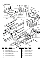
MD DIGITAL BOARD, MD MECHANISM DECK (MDM-7X2A)
1 two screws
(BVTT3 × 6)
2 lug
1 two screws
(BVTT3 × 6)
A
3 Remove the shield case (upper),
in the direction of arrow A .
4 wire (flat type)
(17 core) (CN1004)
7 MD DIGITAL board
8 four step screws
(BVTTWH M3)
qa MD mechanism deck
(MDM-7X2A)
q; insulator
9
q; three insulators
22
4 wire (flat type)
(27 core) (CN1003)
5 connector (CN1006)
6 screw (BVTT3 × 6)
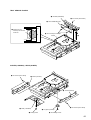
BD (MD) BOARD
1 Remove the solder (four portions).
3
5 BD (MD) board
4 flexible board (CN101)
1 Remove the solder (five portions).
2 two screws (BTP2 × 6)
HOLDER ASSY
1 claw
2 holder assy
23
GUIDE (L), SLIDER (EJ), SLIDER, LEVER (HEAD)
4 slider (EJ)
3 slider
2 guide (L)
1 two screws
(BTP2 × 6)
6 lever (head)
5 lever (CHG)
OPTICAL PICK-UP (KMS-262A/J1N), OVER WRITE HEAD (HR901)
9 optical pick-up (KMS-262A/J1N)
over write head (HR901)
8 main shaft
7 screw (KTP2 × 6)
7 screw
(KTP2 × 6)
5 screw (B2 × 6)
3 screw (B2 × 6)
6 base (BU-A)
4 base (BU-D)
2 gear (SD)
1 screw
(M1.7, TAPPING)
24
SPINDLE MOTOR ASSY (M101), SLED MOTOR ASSY (M102), LOADING MOTOR ASSY (M103)
1 belt (loading)
4 two screws
(PWH1.7 × 2.5)
2 two screws
(PWH1.7 × 2.5)
3 loading motor assy
(M103)
5 sled motor assy
(M102)
7 spindle motor assy
(M101)
6 three screws
(M1.7)
REG BOARD, AMP BOARD, HEAT SINK
1 two connectors
(CN801, 803)
4 screw (BVTT3 × 6)
1 connector (CN852)
5 REG board, AMP board,
heat sink
1 two connectors
(CN904, 907)
1 two connectors
(CN802, 908)
2 two screws (BVTT3 × 6)
3 harness
25
POWER BOARD, POWER TRANSFORMER (T901)
4 connector (CN905)
7 four screws (BVTT3 × 6)
2 two screws
(BVTP3 × 8)
4 connector (CN903)
1 connector (CN901)
6 connector (CN802)
6 connector
(CN904)
5 POWER board
3
8 power transformer
(T901)
CD BASE UNIT (BU-21BD53)
2 bracket
9 three insulators
3 wire (flat type) (21 core)
(CN792)
9 insulator
1 three screws
(BVTP3 × 6)
8 three cone coil
spring
7 collar (damper)
6 three screws
(BVTT2.6 × 6)
26
5 cone coil spring
4 floating screw
(PTPWH M2.6)
0 CD base unit (BU-21BD53)
CD MECHANISM DECK (CDM63-21BD53)
4 screw (BVTT3 × 6)
5 chassis assy
2 connector (CN701)
6 CD mechanism deck
(CDM63-21BD53)
A
4 screw (BVTT3 × 6)
A
3 two screws
(BVTP3 × 8)
3 two screws
(BVTP3 × 8)
1 wire (flat type) (21 core)
(CN791)
RELAY BOARD
3 RELAY board
1 wire (flat type) (21core)
(CN792)
2 two screws
(BTTP M2.6)
27
DRIVER BOARD
3 DRIVER board
1 connector (CN703)
1 connector (CN704)
1 connector (CN702)
2 screw (BTTP M2.6)
2 screw (BTTP M2.6)
1 connector (CN705)
FITTING BASE (STABILIZER) ASSY, TRAY ASSY, TRAY (SUB)
1 two screws (BTTP M2.6)
4 fitting base (STABILIZER) assy
2
2
1 two screws (BTTP M2.6)
5 tray assy, tray (sub)
3 two bosses
3 two bosses
28
TRAY SENSOR BOARD
6 HOLDER (SENSOR)
2 two screws (BTTP M2.6)
5 TRAY SENSOR board
cam
1 Rotate the cam,
and lift up the stocker
at the full.
4 two screws (BTTP M2.6)
stocker
3
SLIDER (LOADING), GEAR (SLIDER)
3 two screws (BTTP M2.6)
4 bracket (retainer)
2 bracket (retainer)
6 slider (LOADING)
5 floating screw
1 two screws (BTTP M2.6)
8 two gears (SLIDER)
7 two floating screws
29
STOCKER ASSY, TRAY (SUB)
3 stocker assy, tray (sub)
1 screw (M2.6)
A
A
2 Slide the slider (BU.L),
slider (BU.R) in the direction of
arrow A at the full.
1 screw (M2.6)
DISC SENSOR BOARD
2 CD base unit assy
1
4 DISC SENSOR board
3 two screws (BTTP M2.6)
30
IN OUT SW BOARD
2 two screws (BTTP M2.6)
3 IN OUT SW board
1 connector (CN704)
MOTOR ASSY (M721), MOTOR BOARD
1 belt
2 connector (CN702)
6
motor board bottom view
7 motor assy (M721)
3 Remove two solders.
4 two screws (BTTP M2.6)
5 motor board
31
SECTION 4
TEST MODE
MD SECITON
4-1.
PRECAUTIONS FOR USE OF TEST MODE
• As loading related operations will be performed regardless of the test mode operations being performed, be sure to check that the disc
is stopped before setting and removing it.
Even if the [MD Z] button is pressed while the disc is rotating during continuous playback, continuous recording, etc., the disc will not
stop rotating.
Therefore, it will be ejected while rotating.
Be sure to press the [MD Z] button after pressing the [MENU/NO] button and the rotation of disc is stopped.
4-1-1. Recording laser emission mode and operating buttons
• Continuous recording mode (CREC 2MODE)
• Laser power check mode (LDPWR CHECK)
• Laser power adjustment mode (LDPWR ADJUST)
• Comparison with initial Iop value written in nonvolatile memory (Iop Compare)
• Write current Iop value in read nonvolatile memory using microprocessor (Iop NV Save)
• Traverse (MO) check (EF MO CHECK)
• Traverse (MO) adjustment (EF MO ADJUST)
• When pressing the [REC/REC IT] button.
4-2.
SETTING THE TEST MODE
The following are two methods of entering the test mode.
Procedure 1: 1. Press the I/1 button to turn the power on.
2. Press the [FUNCTION] button to set the MD function.
3. Press three buttons of x , [MD N X ] and Z (CD3) simultaneously.
When the test mode is set, “[Check]” will be displayed. Turning the [ENTER/YES] knob between the following three
groups; ···Tt [Check] Tt [Service] Tt [Develop] Tt ···.
Procedure 2: 1. Press the I/1 button to turn the power on.
2. Press the [FUNCTION] button to set the MD function.
3. Press three buttons of x , [MD N X ] and Z (CD2) simultaneously.
When the test mode is set, “TEMP CHECK” (C12) will be displayed. By setting the test mode using this method, only the
“Check” group of procedure1 can be executed.
Note: Do not use the test mode in the [Develop] group.
If used, the unit may not operate normally.
If the [Develop] group is set accidentally, press the [MENU/NO] button immediately to exit the [Develop] group.
4-3.
RELEASING THE TEST MODE
Press the [REPEAT] button to display “Initialize”, then release the MD test mode.
4-4.
BASIC OPERATIONS OF THE TEST MODE
All operations are performed using the [ENTER/YES] knob/button and [MENU/NO] button.
The functions of knob and buttons are as follows.
Function name
Function
[ENTER/YES] knob
Changes parameters and modes
[ENTER/YES] button
Proceeds onto the next step. Finalizes input
[MENU/NO] button
Returns to previous step. Stops operations
32
4-5.
SELECTING THE TEST MODE
There are 26 types of test modes as shown below. The groups can be switched by turning the [ENTER/YES] knob. After selecting the group
to be used, press the [ENTER/YES] button. After setting a certain group, turning the [ENTER/YES] knob switches modes shown below.
Refer to “Group” in the table for details can be selected.
All items used for servicing can be treated using group [Service]. So be carefully not to enter other groups by mistake.
Note: Do not use the test mode in the [Develop] group.
If used, the unit may not operate normally.
If the [Develop] group is set accidentally, press the [MENU/NO] button immediately to exit the [Develop] group.
Group
Display
No.
Details
AUTO CHECK
C01
Automatic self-diagnosis
Err Display
C02
Error history display, clear
TEMP ADJUST
C03
Temperature compensation offset adjustment
LDPWR ADJUST
C04
Laser power adjustment
Iop Write
C05
Iop data writing
Iop NV Save
C06
Writes current Iop value in read nonvolatile memory using microprocessor
EF MO ADJUST
C07
Traverse (MO) adjustment
EF CD ADJUST
C08
Traverse (CD) adjustment
FBIAS ADJUST
C09
Focus bias adjustment
AG Set (MO)
C10
Auto gain output level adjustment (MO)
AG Set (CD)
C11
Auto gain output level adjustment (CD)
TEMP CHECK
C12
Temperature compensation offset check
LDPWR CHECK
C13
Laser power check
EF MO CHECK
C14
Traverse (MO) check
EF CD CHECK
C15
Traverse (CD) check
FBIAS CHECK
C16
Focus bias check
ScurveCHECK
C17
S-curve check
VERIFYMODE
C18
Nonvolatile memory check
DETRK CHECK
C19
Detrack check
0920 CHECK
C25
Most circumference check
Iop Read
C26
Iop data display
Iop Compare
C27
Comparison with initial Iop value written in nonvolatile memory
ADJ CLEAR
C28
Initialization of nonvolatile memory for adjustment values
INFORMATION
C31
Display of microprocessor version, etc.
CPLAY2MODE
C36
Continuous playback mode
CREC 2MODE
C37
Continuous recording mode
Mark
Check
Service
• For details of each adjustment mode, refer to “5. Electrical Adjustments”.
For details of “Err Display”, refer to “Self-Diagnosis Function” on page 2.
• If a different mode has been selected by mistake, press the [MENU/NO] button to release that mode.
• Modes with (×) in the Mark column are not used for servicing and therefore are not described in detail. If these modes are set accidentally, press the [MENU/NO] button to release the mode immediately.
33
4-5-1. Operating the Continuous Playback Mode
1. Entering the continuous playback mode
(1) Set the disc in the unit. (Whichever recordable discs or discs for playback only are available)
(2) Turn the [ENTER/YES] knob to display “CPLAY2MODE” (C36).
(3) Press the [ENTER/YES] button to change the display to “CPLAY2MID”.
(4) When access completes, the display changes to “C =
AD = )”.
Note: The numbers “ ” displayed show you error rates and ADER.
2. Changing the parts to be played back
(1) Press the [ENTER/YES] button during continuous playback to change the display as below.
“CPLAY2MID” t “CPLAY2OUT” t “CPLAY2IN”
When pressed another time, the parts to be played back can be moved.
When access completes, the display changes to “C =
AD = )”.
(2)
Note: The numbers “ ” displayed show you error rates and ADER.
3. Ending the continuous playback mode
(1) Press the [MENU/NO] button. The display will change to “CPLAY2MODE” (C36).
(2) Press the [MD Z] button and take out the disc.
Note: The playback start addresses for IN, MID, and OUT are as follows.
IN : 40h cluster
MID : 300h cluster
OUT : 700h cluster
4-5-2. Operating the Continuous Recording Mode (Use only when performing self-recording/palyback check)
1. Entering the continuous recording mode
(1) Set a recordable disc in the unit.
(2) Turn the [ENTER/YES] knob to display “CREC 2MODE” (C37).
(3) Press the [ENTER/YES] button to change the display to “CREC 2MID”.
” and “ REC ” lights up.
(4) When access completes, the display changes to “CREC 2(
Note: The numbers “ ” displayed shows you the recording position addresses.
2. Changing the parts to be recorded
(1) When the [ENTER/YES] button is pressed during continuous recording, the display changes as below.
“CREC 2MID” t “CREC 2OUT” t “CREC 2IN”
(2)
When pressed another time, the parts to be recorded can be changed. “ REC ” goes off.
” and “ REC ” lights up.
When access completes, the display changes to “CREC 2(
Note: The numbers “ ” displayed shows you the recording position addresses.
3. Ending the continuous recording mode
(1) Press the [MENU/NO] button. The display changes to “CREC 2MODE” (C37) and “ REC ” goes off.
(2) Press the [MD Z] button and take out the disc.
Note 1: The recording start addresses for IN, MID, and OUT are as follows.
IN : 40h cluster
MID : 300h cluster
OUT : 700h cluster
Note 2: The [MENU/NO] button can be used to stop recording anytime.
Note 3: Do not perform continuous recording for long periods of time above 5 minutes.
Note 4: During continuous recording, be careful not to apply vibration.
4-6.
FUNCTIONS OF OTHER BUTTONS
Function
Contents
MD N X
Sets continuous playback when pressed in the STOP state. When pressed during continuous playback,
the tracking servo turns ON/OFF
x
Stops continuous playback and continuous recording
M of CURSOR knob
The sled moves to the outer circumference only when this is pressed
m of CURSOR knob
The sled moves to the inner circumference only when this is pressed
CD SYNC HIGH SPEED
Switches between the pit and groove modes when pressed
PLAY MODE
Switches the spindle servo mode (CLV S y CLV A)
CD SYNC HIGH SPEED (*1)
Switches the displayed contents each time the button is pressed
MD Z
Ejects the disc
REPEAT
Releases the test mode
*1) Press the [CD SYNC NORM SPEED] button to lights up “IT” indicator, then press the [CD SYNC HIGH SPEED] button.
34
4-7.
TEST MODE DISPLAYS
Each time the [CD SYNC HIGH SPEED] button is pressed, the display changes in the following order.
When CPLAY or CREC are started, the display will forcibly be switched to the error rate display as the initial mode.
1. Mode display
Displays “TEMP ADJUST” (C03), “CPLAY2MODE” (C36), etc.
Mode display
2. Error rate display
Displays the error rate in the following way.
C=
AD = )
C = : Indicates the C1 error.
AD = : Indicates ADER.
Error rate display
Address display
Auto gain display
(Not used in servicing)
3. Address display
The address is displayed as follows. (MO: recordable disc, CD: playback only disc)
h=
s=
(MO pit and CD)
h=
a=
(MO groove)
h = : Indicates the header address.
s = : Indicates the SUBQ address.
a = : Indicates the ADIP address.
Detrack check display
(Not used in servicing)
IVR display
(Not used in servicing)
C1 error and jitter display
(Not used in servicing)
Note: “–” is displayed when servo is not imposed.
AD error and jitter display
(Not used in servicing)
MEANINGS OF OTHER DISPLAYS
Contents
Display
When Lit
When Off
LP2
Servo ON
Servo OFF
4
Tracking servo OFF
Tracking servo ON
REC
Recording mode ON
Recording mode OFF
SYNC, TRACK
CLV low speed mode
CLV normal mode
L-SYNC
ABCD adjustment completed
PROGRAM, [OVER]
Tracking offset cancel ON
TOC
Tracking auto gain OK
REPEAT
Focus auto gain OK
S.F EDIT
Pit
Groove
DISC
High reflection
Low reflection
NORMAL SPEED
CLV S
CLV A
MONO
CLV LOCK
CLV UNLOCK
Tracking offset cancel OFF
35
4-8.
AUTOMATIC SELF-DIAGNOSIS FUNCTION
This test mode performs CREC and CPLAY automatically for mainly checking the characteristics of the optical pick-up.
To perform this test mode, the laser power must first be checked.
Perform AUTO CHECK after the laser power check and Iop Compare.
Procedure:
1. Turn the [ENTER/YES] knob to display “AUTO CHECK” (C01).
2. Press the [ENTER/YES] button. If “LDPWR
” is displayed, it means that the laser power check has not been performed. In this
case, perform the laser power check and Iop Compare, and then repeat from enter the MD test mode.
3. If a disc is in the mechanical deck, it will be ejected forcibly.
“DISC IN” will be displayed in this case. Load a test disc (MDW-74/GA-1) which can be recorded.
4. If a disc is loaded at step 3, the check will start automatically.
5. When “XX CHECK” is displayed, the item corresponding to XX will be performed.
When “06 CHECK” completes, the disc loaded at step 3 will be ejected. “DISC IN” will be displayed. Load the check disc (TDYS-1).
6. When the disc is loaded in step 5, the check will automatically be resumed from “07 CHECK”.
7. After completing to test item 12, check OK or NG will be displayed. If all items are OK, “CHECK ALL OK” will be displayed. If any item
is NG, it will be displayed as “NG:xxxx”.
When “CHECK ALL OK” is displayed, it means that the optical pick-up is normal. Check the operations of other parts (spindle motor,
sled motor, etc.).
When displayed as “NG:xxxx”, it means that the optical pick-up is faulty. In this case, replace the optical pick-up.
4-9.
INFORMATION
Display the software version.
Procedure:
1. Turn the [ENTER/YES] knob to display “INFORMATION” (C31).
2. Press the [ENTER/YES] button.
3. The software version will be displayed.
4. Press the [MENU/NO] button to end this mode.
36
SECTION 5
ELECTRICAL ADJUSTMENTS
MD SECTION
5-1.
PARTS REPLACEMENT AND ADJUSTMENTS
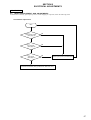
If malfunctions caused by optical pick-up such as sound skipping are suspected, follow the following check.
Check before replacement
Start
5-6-2.
Laser Power Check
(See page 40)
NG
OK
5-6-3.
Iop Compare
(See page 40)
NG
OK
5-6-4.
Auto Check
(See page 41)
NG
Replace optical pick-up or MDM-7X2A
OK
Other faults are suspected.
Check the mechanism parts (spindle motor, sled motor, etc.)
37
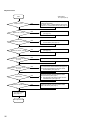
Adjustment flow
• Abbreviation
OP: optical pick-up
Start
Replace IC195
YES
After turning off and then on the power,
initialize the EEPROM
For details, refer to “WHEN MEMORY NG IS DISPLAYED” in 1. SERVICING NOTES (See page 10)
NO
Replace OP or IC195
YES
5-7. INITIAL SETTING OF ADJUSTMENT VALUE
(See page 43)
YES
5-9. TEMPERATURE COMPENSATION OFFSET
ADJUSTMENT (See page 43)
YES
5-10. LASER POWER ADJUSTMENT
(See page 43)
NO
Replace IC101, IC195, or D101
NO
Replace OP, IC190, or IC195
NO
Replace OP, IC102, IC190,
or IC195
YES
5-11. Iop NV SAVE (See page 44)
NO
Replace OP, IC101, IC151,
or IC195
YES
5-12. TRAVERSE ADJUSTMENT (See page 44)
5-13. FOCUS BIAS ADJUSTMENT (See page 45)
5-16. AUTO GAIN CONTROL OUTPUT LEVEL
ADJUSTMENT (See page 46)
NO
Replace OP
YES
“op change” in SELF-DIAGNOSIS FUNCTION
(ITEMS OF ERROR HISTORY MODE ITEMS
AND CONTENTS) (See page 3)
5-8. RECORDING AND DISPLAYING THE IOP
INFORMATION (See page 43)
YES
“spdl change” in SELF-DIAGNOSIS FUNCTION
(ITEMS OF ERROR HISTORY MODE ITEMS
AND CONTENTS) (See page 3)
NO
Replace the spindle motor
NO
5-6-4. Auto Check
(See page 41)
End adjustments
38
5-2.
PRECAUTIONS FOR CHECKING LASER
DIODE EMISSION
To check the emission of the laser diode during adjustments, never
view directly from the top as this may lose your eye-sight.
5-3.
PRECAUTIONS FOR USE OF OPTICAL PICKUP (KMS-262A)
As the laser diode in the optical pick-up is easily damaged by static
electricity, solder the laser tap of the flexible board when using it.
Before disconnecting the connector, desolder first. Before connecting the connector, be careful not to remove the solder. Also
take adequate measures to prevent damage by static electricity.
Handle the flexible board with care as it breaks easily.
pick-up
flexible board
5. When observing several signals on the oscilloscope, etc.,
make sure that VC and ground do not connect inside the oscilloscope.
(VC and ground will become short-circuited)
6. Using the above jig enables the waveform to be checked without the need to solder.
(Refer to Servicing Notes on page 9)
7. As the disc used will affect the adjustment results, make sure
that no dusts nor fingerprints are attached to it.
*1 Laser power meter
When performing laser power checks and adjustment (electrical
adjustment), use of the new MD laser power meter 8010S (Part
No. J-2501-145-A) instead of the conventional laser power meter is convenient.
It sharply reduces the time and trouble to set the laser power
meter sensor onto the objective lens of optical pick-up.
laser tap
Optical pick-up flexible board
5-4. PRECAUTIONS FOR ADJUSTMENTS
1. When replacing the following parts, perform the adjustments
and checks with in the order shown in the following table.
2. Set the MD test mode when performing adjustments.
After completing the adjustments, exit the MD test mode.
Perform the adjustments and checks in “Group Service” of the
MD test mode.
3. Perform the adjustments to be needed in the order shown.
4. Use the following tools and measuring devices.
• Check Disc (TDYS-1) (Part No. : 4-963-646-01)
• Test Disk (MDW-74/GA-1) (Part No. : 4-229-747-01)
• Laser power meter LPM-8001 (Part No. : J-2501-046-A)
or
MD Laser power meter 8010S (Part No. : J-2501-145-A)*1
• Oscilloscope (Measure after performing CAL of prove.)
• Digital voltmeter
• Thermometer
• Jig for checking BD (MD) board waveform
(Part No. : J-2501-196-A)
Parts to be replaced
Adjustment
5-7.
Initial setting of adjustment value
5-8.
Recording of Iop information
5-9.
Temperature compensation
offset adjustment
Optical
Pick-up
IC101
IC102
IC151
IC190
IC195
D101
5-10. Laser power adjustment
5-11. Iop NV Save
5-12. Traverse adjustment
5-13. Focus bias adjustment
5-16. Auto gain adjustment
5-6-4. Auto Check
39
5-5.
USING THE CONTINUOUSLY RECORDED
DISC
* This disc is used in focus bias adjustment and error rate check.
The following describes how to create a continuous recording
disc.
1. Insert a disc (blank disc) commercially available.
2. Turn the [ENTER/YES] knob to display “CREC 2MODE” (C37).
3. Press the [ENTER/YES] button to display “CREC 2 MID”.
Display “CREC 2(0300” and start to recording.
4. Complete recording within 5 minutes.
5. Press the [MENU/NO] button and stop recording .
6. Press the [MD Z] button and remove the disc.
The above has been how to create a continuous recorded data for
the focus bias adjustment and error rate check.
Procedure:
1. Set the laser power meter on the objective lens of the optical
pick-up. (When it cannot be set pr operly, turn the
[CURSOR m ? M ] knob to move the optical pickup.)
Connect the digital volt meter to CN105 pin 1 (I+3V) and
CN105 pin 2 (IOP).
2. Then, turn the [ENTER/YES] knob to display “LDPWR
CHECK” (C13).
3. Press the [ENTER/YES] button once to display “LD
0.9mW$ ”. Check that the reading of the laser power meter
become 0.84 to 0.92 mW.
4. Press the [ENTER/YES] button once more to display “ LD
7.0mW$ ”. Check that the reading the laser power meter and
digital volt meter satisfy the specified value.
Note: Be careful not to apply vibration during continuous recording.
5-6. CHECKS PRIOR TO REPAIRS
These checks are performed before replacing parts according to
“approximate specifications” to determine the faulty locations. For
details, refer to “5-1. Parts Replacement and Adjustments” (see
page 37).
5-6-1. Temperature Compensation Offset Check
When performing adjustments, set the internal temperature and
room temperature to 22 to 28ºC.
Procedure:
1. Turn the [ENTER/YES] knob to display “TEMP CHECK” (C12).
2. Press the [ENTER/YES] button.
3. “T=@@(##) [OK]” should be displayed. If “T=@@ (##) [NG]”
is displayed, it means that the results are bad.
(@@ indicates the current value set, and ## indicates the value
written in the non-volatile memory.)
5-6-2. Laser Power Check
Before checking, check the Iop value of the optical pick-up.
(Refer to 5-8. Recording and Displaying the Iop Information (see
page 43)
Connection:
laser
power meter
digital voltmeter
BD (MD) board
40
(Optical pick-up label)
KMS262A
20101
B0825
For details of the method for
checking this value, refer to
“5-8. Recording and Displaying
the Iop Information”
lOP=82.5 mA in this case
lOP (mA) = Digital voltmeter reading (mV)/1 (Ω)
5. Press the [MENU/NO] button to display “LDPWR CHECK”
(C13) and stop the laser emission.
(The [MENU/NO] button is effective at all times to stop the laser
emission.)
Note: After step 4, each time the [ENTER/YES] button is pressed, the
display will be switched between “LD 0.7W$ ”, “LD
7.5mW$ ”, and “LD Wp
$
”. Nothing needs to be
performed here.
Checking Location: BD (MD) board (see page 47)
5-6-3. Iop Compare
The current Iop value at laser power 7.0 mW output and reference
Iop value (set at shipment) written in the nonvolatile memory are
compared, and the rate of increase/decrease will be displayed in
percentage.
Note: Perform this function with the optical pick-up set at room
temperature.
Optical pick-up
objective lens
CN105 pin 1 (I+3V)
CN105 pin 2 (IOP)
Specified Value:
Laser power meter reading : 7.0 ± 0.2 mW
Digital voltmeter reading : Optical pick-up displayed value ± 10%
+
–
Procedure:
1. Turn the [ENTER/YES] knob to display “Iop Compare” (C27).
2. Press the [ENTER/YES] button and start measurements.
3. When measurements complete, the display changes to “± xx%
yy”.
xx is the percentage of increase/decrease, and OK or NG is
displayed at yy to indicate whether the percentage of increase/
decrease is within the allowable range.
4. Press the [MENU/NO] button to end.
5-6-4. Auto Check
This test mode performs CREC and CPLAY automatically for
mainly checking the characteristics of the optical pick-up. To
perform this test mode, the laser power must first be checked.
Perform Auto Check after the laser power check and Iop compare.
Procedure:
1. Turn the [ENTER/YES] knob to display “AUTO CHECK” (C01).
2. Press the [ENTER/YES] button. If “LDPWR
” is
displayed, it means that the laser power check has not been
performed. In this case, perform the laser power check and Iop
Compare, and then repeat from enter the MD test mode.
3. If a disc is in the mechanical deck, it will be ejected forcibly.
“DISC IN” will be displayed in this case. Load a test disc (MDW74/GA-1) which can be recorded.
4. If a disc is loaded at step 3, the check will start automatically.
5. When “XX CHECK” is displayed, the item corresponding to
XX will be performed.
When “06 CHECK” completes, the disc loaded at step 3 will be
ejected. “DISC IN” will be displayed. Load the check disc
(TDYS-1).
6. When the disc is loaded in the step 5, the check will automatically
be resumed from “07 CHECK”.
7. After completing to test item 12, check OK or NG will be
displayed. If all items are OK, “CHECK ALL OK” will be
displayed. If any item is NG, it will be displayed as “NG: xxxx”.
When “CHECK ALL OK” is displayed, it means that the optical
pick-up is normal. Check the operations of other parts (spindle
motor, sled motor, etc.).
When displayed as “NG: xxxx”, it means that the optical pick-up
is faulty. In this case, replace the optical pick-up.
5-6-5. Other Checks
All the following checks are performed by the Auto Check mode.
They therefore need not be performed in normal operation.
5-6-6. Traverse Check
5-6-7. Focus Bias Check
5-6-8. C PLAY Check
5-6-9. Self-Recording/Playback Check
5-6-6. Traverse Check
Note 1: Data will be erased during MO reading if a recorded disc is
used in this adjustment.
Note 2: If the traverse waveform is not clear, connect the oscilloscope
as shown in the following figure so that it can be seen more
clearly.
oscilloscope
(DC range)
BD (MD) board
330 k Ω
CN105 pin 4 (TE)
CN105 pin 6 (VC)
+
–
10 pF
Connection:
oscilloscope
(DC range)
BD (MD) board
CN105 pin 4 (TE)
CN105 pin 6 (VC)
+
–
V: 0.1 V/div
H: 10 ms/div
Procedure:
1. Connect an oscilloscope to CN105 pin 4 (TE) and CN105
pin 6 (VC) on the BD (MD) board.
2. Load a disc (any available on the market). (Refer to Note 1)
3. Turn the [CURSOR m ? M] knob to move the optical
pick-up outside the pit.
4. Turn the [ENTER/YES] knob to display “EF MO CHECK”
(C14).
5. Press the [ENTER/YES] button to display “EFB = MO-R”.
(Laser power READ power/Focus servo ON/tracking servo
OFF/spindle (S) servo ON)
6. Observe the waveform of the oscilloscope, and check that the
specified value is satisfied. Do not turn the [ENTER/YES]
knob.
(Read power traverse checking)
Traverse Waveform
A
VC
B
Specified value : Below 10% offset value
Offset value (%) = IA – BI X 100
2 (A + B)
7. Press the [ENTER/YES] button to display “EFB =
MOW”.
8. Observe the waveform of the oscilloscope, and check that the
specified value is satisfied. Do not turn the [ENTER/YES]
knob.
(Write power traverse checking)
Traverse Waveform
A
VC
B
Specified value : Below 10% offset value
Offset value (%) = IA – BI X 100
2 (A + B)
41
9. Press the [ENTER/YES] button to display “EFB = MO-P”.
Then, the optical pick-up moves to the pit area automatically
and servo is imposed.
10. Observe the waveform of the oscilloscope, and check that the
specified value is satisfied. Do not turn the [ENTER/YES]
knob.
Traverse Waveform
A
VC
B
Specified value : Below 10% offset value
Offset value (%) = IA – BI X 100
2 (A + B)
11. Press the [ENTER/YES] button to display “EF MO CHECK”
(C14).
The disc stops rotating automatically.
12. Press the [MD Z] button and take out the disc.
13. Load the check disc (TDYS-1).
14. Turn the [ENTER/YES] knob to display “EF CD CHECK”
(C15).
15. Press the [ENTER/YES] button to display “EFB =
CD”.
Servo is imposed automatically.
16. Observe the waveform of the oscilloscope, and check that the
specified value is satisfied. Do not turn the [ENTER/YES]
knob.
Traverse Waveform
A
VC
B
Specified value : Below 10% offset value
Offset value (%) = IA – BI X 100
2 (A + B)
17. Press the [ENTER/YES] button to display “EF CD CHECK”
(C15).
18. Press the [MD Z] button and take out the check disc.
Checking Location: BD (MD) board (see page 47)
5-6-7. Focus Bias Check
Change the focus bias and check the focus tolerance amount.
Procedure:
1. Load the test disc (MDW-74/GA-1).
2. Turn the [ENTER/YES] knob to display “CPLAY2MODE”
(C36).
3. Press the [ENTER/YES] button to display “CPLAY2MID”.
4. Press the [MENU/NO] button when “C =
AD = )” is
displayed.
5. Turn the [ENTER/YES] knob to display “FBIAS CHECK”
(C16).
6. Press the [ENTER/YES] button to display “
/ c = ”.
The first four digits indicate the C1 error rate, the two digits
after [/] indicate ADER, and the 2 digits after [c =] indicate
the focus bias value.
Check that the C1 error is below 20 and ADER is below 2.
7. Press the [ENTER/YES] button to display “
/ b = ”.
Check that the C1 error is about 200 and ADER is below 2.
8. Press the [ENTER/YES] button to display “
/ a = ”.
Check that the C1 error is about 200 and ADER is below 2.
9. Press the [MENU/NO] button, then press the [MD Z] button and
take out the test disc.
5-6-8. C PLAY Check
MO Error Rate Check
Procedure:
1. Load the test disc (MDW-74/GA-1).
2. Turn the [ENTER/YES] knob to display “CPLAY2MODE”
(C36).
3. Press the [ENTER/YES] button to display “CPLAY2MID”.
4. The display changes to “C =
AD = )”.
5. If the C1 error rate is below 20, check that ADER is 00.
6. Press the [MENU/NO] button to stop playback, then press the
[MD Z] button and take out the test disc.
CD Error Rate Check
Procedure:
1. Load the check disc (TDYS-1).
2. Turn the [ENTER/YES] knob to display “CPLAY2MODE”
(C36).
3. Press the [ENTER/YES] button to display “CPLAY2MID”.
4. The display changes to “C =
AD = )”.
5. Check that the C1 error rate is below 20.
6. Press the [MENU/NO] button to stop playback, then press the
[MD Z] button and take out the check disc.
5-6-9. Self-Recording/playback Check
Prepare a continuous recording disc using the unit to be repaired
and check the error rate.
Procedure:
1. Load a recordable disc (blank disc).
2. Turn the [ENTER/YES] knob to display “CREC 2MODE”
(C37).
3. Press the [ENTER/YES] button to display “CREC 2MID”.
4. When recording starts, lights up “ REC ” and display “CREC
2 @@@@” (@@@@ is the address).
5. About 1 minute later, press the [MENU/NO] button to stop
continuous recording.
6. Turn the [ENTER/YES] knob to display “CPLAY2MODE”
(C36).
7. Press the [ENTER/YES] button to display “CPLAY2 MID”.
8. “C =
AD = )” will be displayed.
9. Check that the C1 error becomes below 20 and the AD error
below 2.
10. Press the [MENU/NO] button to stop playback, then press the
[MD Z] button and take out the disc.
42
5-7.
INITIAL SETTING OF ADJUSTMENT VALUE
5-9.
TEMPERATURE COMPENSATION OFFSET
ADJUSTMENT
Note:
Mode which sets the adjustment results recorded in the non-volatile
memory to the initial setting value. However the results of the temperature compensation offset adjustment will not change to the initial setting
value.
If initial setting is performed, perform all adjustments again excluding the
temperature compensation offset adjustment.
For details of the initial setting, refer to “5-4. Precautions for Adjustments”
(See page 39) and execute the initial setting before the adjustment as
required.
Save the temperature data at that time in the non-volatile memory
as 25 ˚C reference data.
Procedure:
1. Turn the [ENTER/YES] knob to display “ADJ CLEAR” (C28).
2. Press the [ENTER/YES] button. “Complete!” will be displayed
momentarily and initial setting will be executed, after which
“ADJ CLEAR” (C28) will be displayed.
Procedure:
1. Turn the [ENTER/YES] knob to display “TEMP ADJUST”
(C03).
2. Press the [ENTER/YES] button to select the “TEMP ADJUST”
mode.
3. “TEMP =
[OK]” and the current temperature data will be
displayed.
4. To save the data, press the [ENTER/YES] button.
When not saving the data, press the [MENU/NO] button.
5. When the [ENTER/YES] button is pressed, “TEMP =
SAVE” will be displayed and turned back to “TEMP ADJUST”
(C03) display then. When the [MENU/NO] button is pressed,
“TEMP ADJUST” (C03) will be displayed immediately.
5-8.
RECORDING AND DISPLAYING THE IOP
INFORMATION
The IOP data can be recorded in the non-volatile memory. The
IOP value on the optical pick-up label and the IOP value after the
adjustment will be recorded. Recording these data eliminates the
need to read the label on the optical pick-up.
Recording Procedure:
1. Turn the [ENTER/YES] knob to display “Iop Write” (C05),
and press the [ENTER/YES] button.
2. The display becomes “Ref=@@@.@” (@ is an arbitrary number) and the numbers which can be changed will blink.
3. Input the IOP value on the optical pick-up label.
To select the number : Turn the [ENTER/YES] knob.
To select the digit : Press the [CD SYNC NORM SPEED]
button to lights up “IT” indicator, then press the [REC MODE]
button.
4. When the [ENTER/YES] button is pressed, the display becomes “Measu=@@@.@” (@ is an arbitrary number).
5. As the adjustment results are recorded for the step 4 value.
Leave it as it is and press the [ENTER/YES] button.
6. “Complete!” will be displayed momentarily. The value will be
recorded in the non-volatile memory and the display will become “Iop Write” (C05).
Note:
1. Usually, do not perform this adjustment.
2. Perform this adjustment in an ambient temperature of 22 ˚C to 28 ˚C.
Perform it immediately after the power is turned on when the internal
temperature of the unit is the same as the ambient temperature of 22 ˚C
to 28 ˚C.
3. When D101 has been replaced, perform this adjustment after the temperature of this part has become the ambient temperature.
Specified Value:
The “TEMP =
” should be within “E0 - EF”, “F0 - FF”, “00 0F”, “10 - 1F” and “20 - 2F”.
5-10. LASER POWER ADJUSTMENT
Check the IOP value of the optical pick-up before adjustments.
(Refer to 5-8. Recording and Displaying the Iop Information)
Connection:
laser
power meter
Optical pick-up
objective lens
digital voltmeter
Display Procedure:
1. Turn the [ENTER/YES] knob to display “Iop Read”(C26).
2. “@@.@/##.#” is displayed and the recorded contents are displayed.
@@.@ indicates the IOP value on the optical pick-up label.
##.# indicates the IOP value after adjustment
3. To end, press the [MENU/NO] button to display “Iop Read”
(C26).
BD (MD) board
CN105 pin 1 (I+3V)
CN105 pin 2 (IOP)
+
–
Procedure:
1. Set the laser power meter on the objective lens of the
optical pick-up. (When it cannot be set properly, turn the
[CURSOR m ? M] knob to move the optical pickup)
Connect the digital voltmeter to CN105 pin 1 (I+3V) and
CN105pin 2 (IOP) on the BD (MD) board.
2. Turn the [ENTER/YES] knob to display “LDPWR ADJUST”
(C04).
(Laser power : For adjustment)
3. Press the [ENTER/YES] button once to display “LD 0.9 mW
$ ”.
4. Turn the [ENTER/YES] knob so that the reading of the laser
power meter becomes 0.85 to 0.91 mW. Press the [ENTER/YES]
button after setting the range knob of the laser power meter, and
save the adjustment results. (“LD SAVE $ ” will be displayed
for a moment)
5. Then “LD 7.0 mW $ ” will be displayed.
43
6. Turn the [ENTER/YES] knob so that the reading of the laser
power meter becomes 6.9 to 7.1 mW, press the [ENTER/YES]
button to save it.
Note: Do not perform the emission with 7.0 mW more than 15 seconds
continuously.
7. Then, turn the [ENTER/YES] knob to display “LDPWR
CHECK” (C13).
8. Press the [ENTER/YES] button once to display “LD 0.9mW$
”. Check that the reading of the laser power meter become
0.85 to 0.91 mW.
9. Press the [ENTER/YES] button once more to display “LD
7.0mW$ ”. Check that the reading the laser power meter
and digital voltmeter satisfy the specified value.
Note down the digital voltmeter reading value.
Specified Value:
Laser power meter reading : 7.0 ± 0.2 mW
Digital voltmeter reading : Value on the optical pick-up label
±10%
(Optical pick-up label)
KMS262A
20101
B0825
For details of the method for
checking this value, refer to
“5-8. Recording and Displaying
the Iop Information”
lOP=82.5 mA in this case
lOP (mA) = Digital voltmeter reading (mV)/1 (Ω)
10. Press the [MENU/NO] button to display “LDPWR CHECK”
(C13) and stop the laser emission.
(The [MENU/NO] button is effective at all times to stop the
laser emission)
11. Turn the [ENTER/YES] knob to display “Iop Write” (C05).
12. Press the [ENTER/YES] button. When the display becomes
Ref=@@@.@ (@ is an arbitrary number), press the
[ENTER/YES] button to display “Measu=@@@.@” (@ is
an arbitrary number).
13. The numbers which can be changed will blink. Input the Iop
value noted down at step 9.
To select the number : Turn the [ENTER/YES] knob.
To select the digit : Press the [CD SYNC NORM SPEED] button
to lights up “IT” indicator, then press the [REC MODE] button.
14. When the [ENTER/YES] button is pressed, “Complete!” will
be displayed momentarily. The value will be recorded in the
non-volatile memory and the display will become “Iop Write”
(C05).
Note: After step 4, each time the [ENTER/YES] button is pressed, the
display will be switched “LD 0.7mW$
”, “LD 7.5mW$
”,
and “LD Wp
$ ”. Nothing needs to be performed here.
4. After “Complete!” is displayed momentarily, the display changes
to “Iop 7.0 mW”.
5. After the display changes to “Iop=yysave?”, press the
[ENTER/YES] button.
6. When “Complete!” is displayed, it means that Iop NV saving
has been completed.
5-12. TRAVERSE ADJUSTMENT
Note 1:Data will be erased during MO reading if a recorded disc is
used in this adjustment.
Note 2:If the traverse waveform is not clear, connect the oscilloscope
as shown in the following figure so that it can be seen more
clearly.
oscilloscope
(DC range)
BD (MD) board
330 k Ω
CN105 pin 4 (TE)
+
–
CN105 pin 6 (VC)
10 pF
Connection:
oscilloscope
(DC range)
BD (MD) board
CN105 pin 4 (TE)
CN105 pin 6 (VC)
+
–
V: 0.1 V/div
H: 10 ms/div
Procedure:
1. Connect an oscilloscope to CN105 pin 4 (TE) and CN105
pin 6 (VC) on the BD (MD) board.
2. Load a disc (any available on the market). (Refer to Note 1)
3. Turn the [CURSOR m ? M] knob to move the optical
pick-up outside the pit.
4. Turn the [ENTER/YES] knob to display “EF MO ADJUST”
(C07).
5. Press the [ENTER/YES] button to display “EFB = MO-R”.
(Laser power READ power/Focus servo ON/tracking servo
OFF/spindle (S) servo ON)
6. Turn the [ENTER/YES] knob so that the waveform of the oscilloscope becomes the specified value.
(When the [ENTER/YES] knob is turned, the
of “EFB=
” changes and the waveform changes) In this adjustment,
waveform varies at intervals of approx. 2%. Adjust the waveform so that the specified value is satisfied as much as possible.
(Read power traverse adjustment)
Traverse Waveform
Adjustment Location: BD (MD) board (see page 47)
A
5-11. Iop NV SAVE
Write the reference values in the nonvolatile memory to perform
“Iop compare”. As this involves rewriting the reference values, do
not perform this procedure except when adjusting the laser power
during replacement of the optical pick-up and when replacing the
IC102. Otherwise the optical pick-up check may deteriorate.
Note: Perform this function with the optical pick-up set at room
temperature.
Procedure:
1. Turn the [ENTER/YES] knob to display “Iop NV Save” (C06).
2. Press the [ENTER/YES] button and display “Iop [stop]”.
3. After the display changes to “Iop =xxsave?”, press the
[ENTER/YES] button.
44
VC
B
Specification A = B
7. Press the [ENTER/YES] button and save the result of adjustment to the non-volatile memory (“EFB =
SAVE” will be
displayed for a moment. Then “EFB = MO-W” will be displayed).
8. Turn the [ENTER/YES] knob so that the waveform of the oscilloscope becomes the specified value.
(When the [ENTER/YES] knob is turned, the
of “EFB=
” changes and the waveform changes) In this adjustment,
waveform varies at intervals of approx. 2%. Adjust the waveform so that the specified value is satisfied as much as possible.
(Write power traverse adjustment)
18. Press the [ENTER/YES] button, display “EFB =
SAVE”
for a moment and save the adjustment results in the non-volatile
memory.
Next “EF CD ADJUST” (C08) will be displayed.
19. Press the [MD Z ] button and take out the check disc.
Adjustment Location: BD (MD) board (see page 47)
5-13. FOCUS BIAS ADJUSTMENT
Traverse Waveform
A
VC
B
Specification A = B
9. Press the [ENTER/YES] button, and save the adjustment results
in the non-volatile memory. (“EFB =
SAVE” will be displayed for a moment)
10. “EFB =
MO-P” will be displayed.
The optical pick-up moves to the pit area automatically and
servo is imposed.
11. Turn the [ENTER/YES] knob until the waveform of the oscilloscope moves closer to the specified value.
In this adjustment, waveform varies at intervals of approx. 2%.
Adjust the waveform so that the specified value is satisfied as
much as possible.
Traverse Waveform
A
VC
B
Specification A = B
12. Press the [ENTER/YES] button, and save the adjustment results
SAVE” will be disin the non-volatile memory. (“EFB =
played for a moment)
Next “EF MO ADJUST” (C07) is displayed. The disc stops
rotating automatically.
13. Press the [MD Z] button and take out the disc.
14. Load the check disc (TDYS-1).
15. Turn the [ENTER/YES] knob to display “EF CD ADJUST”
(C08).
16. Press the [ENTER/YES] button to display “EFB =
CD”.
Servo is imposed automatically.
17. Turn the [ENTER/YES] knob so that the waveform of the oscilloscope moves closer to the specified value.
In this adjustment, waveform varies at intervals of approx. 2%.
Adjust the waveform so that the specified value is satisfied as
much as possible.
Procedure:
1. Load the continuously-recorded disc. (Refer to “5-5. USING
THE CONTINUOUSLY RECORDED DISC” (See page 40))
2. Turn the [ENTER/YES] knob to display “CPLAY2 MODE”
(C36).
3. Press the [ENTER/YES] button to display “CPLAY2MID”.
4. Press the [MENU/NO] button when “C =
AD = )” is
displayed.
5. Turn the [ENTER/YES] knob to display “FBIAS ADJUST”
(C09).
6. Press the [ENTER/YES] button to display “
/ a = ”.
The first four digits indicate the C1 error rate, the two digits
after “/ ” indicate ADER, and the 2 digits after “a =” indicate
the focus bias value.
7. Turn the [ENTER/YES] knob in the clockwise and find the
focus bias value at which the C1 error rate becomes about 200
(refer to Note 2).
8. Press the [ENTER/YES] button to display “
/ b = ”.
9. Turn the [ENTER/YES] knob in the counterclockwise and find
the focus bias value at which the C1 error rate becomes about
200.
10. Press the [ENTER/YES] button to display “
/ c = ”.
11. Check that the C1 error rate is below 20 and ADER is 00.
Then press the [ENTER/YES] button.
12. If the “( )” in “ ( )” is above 20, press the
[ENTER/YES] button.
If below 20, press the [MENU/NO] button and repeat the adjustment from step 2.
13. Press the [MD Z] button and take out the disc.
Note 1: The relation between the C1 error and focus bias is as shown in
the following figure. Find points A and B in the following figure
using the above adjustment. The focal point position C is automatically calculated from points A and B.
Note 2: As the C1 error rate changes, perform the adjustment using the
average vale.
C1 error
about
200
Focus bias value
B
C
A
Traverse Waveform
A
VC
B
Specification A = B
45
5-14. ERROR RATE CHECK
5-16. AUTO GAIN CONTROL OUTPUT LEVEL
ADJUSTMENT
5-14-1. CD Error Rate Check
Procedure:
1. Load the check disc (TDYS-1).
2. Turn the [ENTER/YES] knob to display “CPLAY2 MODE”
(C36).
3. Press the [ENTER/YES] button twice and display “CPLAY2
MID”.
4. The display changes to “C =
AD = )”.
5. Check that the C1 error rate is below 20.
6. Press the [MENU/NO] button to stop playback, then press the
[MD Z] button and take out the check disc.
Be sure to perform this adjustment when the optical pick-up is
replaced.
If the adjustment results becomes “Adjust NG!”, the optical pickup may be faulty or the servo system circuits may be abnormal.
5-14-2. MO Error Rate Check
Procedure:
1. Load the continuously-recorded disc. (Refer to “5-5. USING
THE CONTINUOUSLY RECORDED DISC” (See page 40))
2. Turn the [ENTER/YES] knob to display “CPLAY2 MODE”
(C36).
3. Press the [ENTER/YES] button to display “CPLAY2MID”.
4. The display changes to “C =
AD = )”.
5. If the C1 error rate is below 20, check that ADER is 00.
6. Press the [MENU/NO] button to stop playback, then press the
[MD Z] button and take out the disc.
5-15. FOCUS BIAS CHECK
Change the focus bias and check the focus tolerance amount.
Procedure:
1. Load the continuously-recorded disc. (Refer to “5-5. USING
THE CONTINUOUSLY RECORDED DISC” (See page 40))
2. Turn the [ENTER/YES] knob to display “CPLAY2 MODE”
(C36).
3. Press the [ENTER/YES] button twice to display “CPLAY2
MID”.
4. Press the [MENU/NO] button when “C =
AD = )” is
displayed.
5. Turn the [ENTER/YES] knob to display “FBIAS CHECK”
(C16).
6. Press the [ENTER/YES] button to display “
/ c = ”.
The first four digits indicate the C1 error rate, the two digits
after “/ ” indicate ADER, and the 2 digits after “c =” indicate
the focus bias value.
Check that the C1 error is below 20 and ADER is below 2.
7. Press the [ENTER/YES] button and display “
/ b = ”.
Check that the C1 error is below 200 and ADER is below 2.
8. Press the [ENTER/YES] button and display “
/ a = ”.
Check that the C1 error is below 200 and ADER is below 2
9. Press the [MENU/NO] button, then press the [MD Z] button
and take out the disc.
Note:
46
If the C1 error and ADER are above other than the specified
value at points a (step 8. in the above) or b (step 7. in the above),
the focus bias adjustment may not have been carried out properly. Adjust perform the beginning again.
5-16-1. CD Auto Gain Control Output Level Adjustment
Procedure:
1. Load the check disc (TDYS-1).
2. Turn the [ENTER/YES] knob to display “AG Set (CD)” (C11).
3. When the [ENTER/YES] button is pressed, the adjustment will
be performed automatically.
“Complete!” will then be displayed momentarily when the
value is recorded in the non-volatile memory, after which the
display changes to “AG Set (CD)” (C11).
4. Press the [MD Z] button and take out the check disc.
5-16-2. MO Auto Gain Control Output Level Adjustment
Procedure:
1. Load the test disc (MDW-74/GA-1).
2. Turn the [ENTER/YES] knob to display “AG Set (MO)” (C10).
3. When the [ENTER/YES] button is pressed, the adjustment will
be performed automatically.
“Complete!” will then be displayed momentarily when the
value is recorded in the non-volatile memory, after which the
display changes to “AG Set (MO)” (C10).
4. Press the [MD Z] button and take out the test disc.
Adjustment and checking Loacation:
CD SECTION
– BD (MD) BOARD (Component Side) –
Note:
1. CD Block is basically designed to operate without adjustment. Therefore, check each item in order given.
2. Use YEDS-18 disc (3-702-101-01) unless otherwise indicated.
3. Use an oscilloscope with more than 10MΩ impedance.
4. Clean the object lens by an applicator with neutral detergent when the
signal level is low than specified value with the following checks.
5. Level doesn’t change whichever with normal speed or with four times
speed.
D101
CN101
S Curve Check
Connection:
oscilloscope
(DC range)
BD (CD) board
TP (FE)
TP (VC)
+
–
Procedure:
1. Connect an oscilloscope to test point TP (FE) and TP (VC) on
the BD (CD) board.
2. Turn the power on.
3. Put the disc (YEDS-18) in and turned power switch on again
and actuate the focus search. (actuate the focus search when disc
table is moving in and out)
4. Check the oscilloscope waveform (S-curve) is symmetrical
between A and B. And confirm peak to peak level within 3.6 ±
0.5 Vp-p.
– BD (MD) BOARD (Conductor Side) –
IC101
S-curve waveform
symmetry
IC151
CN105
1. I+3V
1
2. IOP
7
3. GND
4. TE
5. FE
6. VC
7. RF
IC190
A
within 3.6 ± 0.5 Vp-p
B
Note: • Try to measure several times to make sure than the ratio of A : B
or B : A is more than 10 : 7.
• Take sweep time as long as possible and light up the
brightness to obtain best waveform.
Checking Location: BD (CD) board (see page 48)
RF Level Check
Connection:
Note: It is useful to use the jig for checking BD (MD) board waveform.
(Refer to Servicing Notes on page 9)
oscilloscope
(AC range)
BD (CD) board
TP (RF)
TP (VC)
+
–
Procedure:
1. Connect an oscilloscope to test point TP (RF) and TP (VC) on
the BD (CD) board.
2. Turn the power on.
3. Put the disc (YEDS-18) in to playback the number five track.
4. Confirm that oscilloscope waveform is clear and check RF signal level is correct or not.
47
Note: A clear RF signal waveform means that the shape “◊” can be clearly
distinguished at the center of the waveform.
Checking Location:
– BD (CD) BOARD (Conductor Side) –
RF signal waveform
VOLT/DIV: 200 mV
TIME/DIV: 500 ns
(normal speed)
level: 1.2 ±0.2 Vp-p
TP
(VC)
IC171
TP
(FE)
Checking Location: BD (CD) board
TP (TE)
TP (RF)
E-F Balance Check
Connection:
oscilloscope
(DC range)
BD (CD) board
TP (TE)
TP (VC)
+
–
Procedure:
1. Connect an oscilloscpe to test point TP (TE) and TP (VC) on the
BD (CD) board.
2. Turn the power on.
3. Put the disc (YEDS-18) in to playback the number five track.
4. Press the [REPEAT] button. (The tracking servo and the sledding servo are turned OFF)
5. Check the level B of the oscilliscope's waveform and the A (DC
voltage) of the center of the Traverse waveform.
Confirm the following :
A/B x 100 = less than ± 22%
Traverse Waveform
Center of
the waveform
B
A (DC
voltage)
0V
level: 1.3 ± 0.6 Vp-p
6. Press the [REPEAT] button. (The tracking servo and sledding
servo are turned ON)
Confirm the C (DC voltage) is almost equal to the A (DC voltage) is step 5.
Traverse Waveform
C (DC
voltage)
0V
Tracking servo
Sled servo
OFF
Checking Location: BD (CD) board
48
Tracking servo
Sled servo
ON
IC101
HCD-PX5
SECTION 6
DIAGRAMS
BLOCK DIAGRAM – MD SERVO Section –
DIGITAL SIGNAL PROCESSOR,
EFM/ACIRC ENCODER/DECODER,
SHOCK PROOF MEMORY CONTROLLER,
ATRAC ENCODER/DECODER
IC151 (1/2)
OVER WRITE
HEAD DRIVE
IC181, Q181, 182
100
1
2
53
MORFI
MORFO
I
RF AMP
J
FILI
60
PCO
59
CLTV
62
FILO
61
54
RFO
46
40
AGCI
RF
RF AGC
& EQ
57
38
PLL
ASYO
ATRAC
ENCODER/DECODER
FILTER
RF AMP,
FOCUS/TRACKING ERROR AMP
IC101
48 47
I
DADTI
25
A
(Page 50)
B
(Page 50)
DIN0
C
(Page 50)
DOUT
D
(Page 50)
DATAI
SCTX
J
ADDT
EFMO
SHOCK PROOF
MEMORY CONTROLLER
HR901
OVER WRITE HEAD
15
TX
EFM/ACIRC
ENCODER/DECODER
6-1.
SAMPLING
22
RATE
CONVERTER XBCKI
24
LRCKI
23
DIGITAL
AUDIO
INTERFACE
DIN0
19
DIN1
20
DOUT
21
ASYI
DADT
COMPARATOR
RFI
LRCK, BCK
BCK
LRCK
26
EQ
CLOCK
GENERATOR
BOTM
ADIN
ADFG
B
OSCI
OSCO
36
C
D
E
8
9
F
I-V
AMP
ABCD
ABCD
AMP
FE
FOCUS
ERROR AMP
E
F
TE
TRACKING
ERROR AMP
I-V
AMP
SE
35
34
79
F0CNT
CPU
INTERFACE
SPINDLE
SERVO
26
28
94 93 10
LASER DIODE
12
11
14
9 8
5 6 7
SHOCK
XBUSY
38 42 50
58 56
MNT1 (SHOCK)
MNT2 (XBUSY)
COMPARATOR
IC102
SRDT
16 17 18
XINT
SENS
20
OPTICAL PICK-UP BLOCK
(KMS-262A/J1N)
SQSY
25 27 32 48 40
12
133 OP-LEVEL
FOCUS/TRACKING COIL DRIVE,
SPINDLE/SLED MOTOR DRIVE
IC141
MD MECHANISM CONTROLLER
IC1001 (1/2)
13
RECP
83
M102
(SLED)
(FOCUS)
(TRACKING)
FCS+
M
27 OUT2F
25 OUT2R
21 OUT1F
23 OUT1R
IN2F 29
IN2R 30
IN1F 19
IN1R 18
APCREF
AUTOMATIC
POWER
CONTROL
SFDR
92
SRDR
91
FFDR
88
FRDR
89
IN3F 14
IN3R 15
TFDR
86
TRDR
85
LDIN
12
13
• SIGNAL PATH
: MD PLAY
: MD REC
: CD PLAY
S101
(LIMIT IN)
ON: When the optical pick-up is
inner position
LIMIT-IN 30
S105
S105
(REC POSITION)
ON: When the over write head is
recording position
REC-SW 43
S103
(PACK OUT)
LOADING
MOTOR DRIVE
IC1004
VREF 4
OUT1 OUT2
2
ON: When the eject slider is
open position
OUT-SW 51
M+7V
6
IN2
5
IN1
ANALOG MUX
REFERENCE
VOLTAGE SWITCH
Q1001, 1002
S104
S104
(PLAY POSITION)
ON: When the eject slider is
playback position
PLAY-SW 49
10
11 LD-LOW
M
FROM CPU
INTERFACE
AUTO
SEQUENCER
12 OUT3F
10 OUT3R
OE
WE
RAS
CAS
S103
A/D CONVERTER
DIGITAL
SERVO
SIGNAL
PROCESS
FCS–
TRK+
TRK–
22
4
5
23
67 65 66 75 74 63 64
AUX1
ABCD
FE
TE
SE
PEAK
BOTM
SPFD
SPRD
PWM GENERATOR
IN4R 3
IN4F 4
LDOUT
14 MOD
6 OUT4F
8 OUT4R
43
47
46
44
47 DIG-RST
35 WRPWR
M
D-RAM
IC152
S101
29 LDON
PSB 16
M101
(SPINDLE)
17
SWDT
SCLK
XLAT
PD
F0CNT
10
APCREF
LASER ON
SWITCH
Q101
PD
XOE
XWE
XRAS
XCAS
SERIAL/
PARALLEL
CONVERTER,
DECODER
V-I
CONVERTER
HF MODULE
1 2 3 4
SWDT
SCLK
XLAT
LD/PD
AMP
DQSY
APC
11
WBL
3T
EQ
AUTOMATIC
POWER
CONTROL
Q121, 122
LD
2-AXIS
DEVICE
MONITOR
CONTROL
COMMAND
ILCC
PD
78
32
D0 – D3
30
A00 – A10
DETECTOR
29
B.P.F.
MNT0
MNT1
MNT2
MNT3
E
A
B
C
D
INTERNAL BUS
SWDT
SCLK
XLAT
4
5
6
7
SUBCODE
PROCESSOR
ADIP
DEMODULATOR/
DECODER
SENS
SRDT
A
ADFM
AT
AMP
XINT
J
SQSY
A
XRST
DQSY
B
SPRD
C
D
SPFD
I
ADFG
WBL
X171
90.3168MHz
16
2, 3, 24, 25
DQ1 – DQ4
PEAK
PEAK &
BOTTOM
9 – 12, 15 – 19, 21, 8
A0 – A10
TEMP
49, 48, 50, 51
37
WBL
3T
F
34 – 31, 36 – 40, 45, 35
33
XBCK
LRCK
FS256
28 27 29
AUX
B.P.F.
M103
(LOADING)
XLRF
CKRF
DTRF
XLAT
80
SCLK
81
SWDT
82
REFLECT 67
EEPROM
IC195
SDA
SCL
WP
DIGITAL SERVO
SIGNAL PROCESSOR
IC151 (2/2)
HF MODULE
SWITCH
Q131 – 134
MOD
05
49
49
PROTECT 68
5
6
7
61 SDA
66 SCL
60 EEP-WP
–1
S102-1
(REFLECT RATE DETECT)
ON: When the high reflection
rate disc detect
–2
S102
S102-2
(PROTECT DETECT)
ON: When the REC-proof claw is
close (un-protect)
HCD-PX5
BLOCK DIAGRAMS – D/A, A/D CONVERTER Section –
VINL
13
DIGITAL
INTERFACE
DCCANCELLATION
FILTER
A/D
CONVERTER
BLOCK
DECIMATION
FILTER
11
: MD PLAY
DIN0
SPDIF1
SLSEL
LOCK
D/A
CONVERTER
BLOCK
VOUTL
VOUTR
LOUT
18
22
RESET 1
MUTE
12
21
LDON
X1 – X4
X1 – X2
SPDL MUTE
13
19
18
22
LDON
X4
CTRL1
SPINDLE MUTE
AMUTE 30
8 MUTE
AC-OUT 93
26 P.DOWN
RESET 34
39 X1
LOD-POS 54
LOD-NEG 55
FIN
7
RIN
9
MOTOR
DRIVE
TRAYSENS1 50
SUB TRAY1
HEIGHT SENSOR
IC731
TRAYSENS2 51
SUB TRAY2
HEIGHT SENSOR
IC732
TRAYSENS3 47
SUB TRAY3
HEIGHT SENSOR
IC733
X101
16MHz
(Page 51)
F
M
M721
(LOADING)
XOUT 20
I2CDAT
3
37 I2CDAT
I2CCLK
5
36 I2CCLK
I2CHELP 89
I2CHELP 90
115 I2CBUSY
IICDATA
31 BDPWR
XIN 22
ON: When sub tray slides out
of the chucking position
IICDATA, IICCLK
IICHELP
05
4
2
S741
(IN)
IN-SW 53
E
OUT1
OUT2
ON: When sub tray is
chucking position
86 DISC-SENS
Q701
BDPWR
118
S742
(OUT)
OUT-SW 52
(Page 52)
9
MD MECHANISM
CONTROLLER
IC1001 (2/2)
38 X2
DISC IN DETECT
IC751
116
LOADING
MOTOR DRIVE
IC701
32 BDRST
RST
124 10
RESET SWITCH
Q1103
50
50
IICHELP
CD BLOCK
(BU-21BD53)
OP ASSY
(A-MAX. 2)
DATA
CLK
SUBQ
SQCLK
XLT
SENSE
SCOR
IICCLK
DOUT
CD MECHANISM CONTROLLER
IC1101
7
8
15
17
11
12
91
(Page 51)
R-CH
MUTING
Q1103, 1104
CD-DATA
CD-CLK
SQDATA
SQCK
X-LAT
SENS
SCOR
H
LOCK
13
OPTSEL
DATA IN/OUT
INTERFACE
ADPDWN
16
IEC958
DECODER
29
DARST
DIGITAL SIGNAL
SELECT SWITCH
IC1008
CLKOUT
LOCK
OPTICAL
RECEIVER
IC121
SLICERSEL
DIGITAL
OPTICAL IN
CLOCK AND
TIMING CIRCUIT
: OPTICAL IN
OPTSEL
A
15
SPDIF0
: MD REC
D/A CONVERTER
IC1006
NOISE SHAPER
(Page 49 )
D
I2SBCKOUT
(Page 49)
DOUT
• R-ch is omitted due to same as L-ch.
• SIGNAL PATH
7
: CD PLAY
37
(Page 51)
8
LRCK
33
G
R-CH
BCK
INTERPOLATOR
BCK, LRCK
3
12
AUDIO FEATURE
PROCESSOR
C
SCLK
PWON
I2SLRCKOUT
(Page 49)
CLOCK CONTROL
WS
BCK
A/D CONVERTER
IC1005
VINR
LIN
1
DALOCK
B
DAT AO
SLSEL
(Page 49)
DADTI
OPTSEL
SLICERSEL
6-2.
RESET 19
X1001
10MHz
RESET SWITCH
Q601
RESET SIGNAL
GENERATOR
IC601
P.DOWN
B.UP +3.3V
K
(Page 52)
HCD-PX5
6-3.
BLOCK DIAGRAM – MAIN Section –
LIN
G
(Page 50)
J502
BUFFER
IC401
L
TAPE OUT
MUTING
Q501
R-CH
R
+
R-CH
R-CH
J702
R-CH
MUTING
CONTROL
Q511
ANALOG
IN
J701
R-CH
INPUT SELECT SWITCH,
TONE CONTROL,
ELECTRICAL VOLUME
IC505
J501
L
35
R-CH
(Page 50)
H
36
38
37
39
LOUT
TUNER PACK
LINE
TC
CDMD
ST
R-CH
TM801
TONE
CONTROL
CIRCUIT
INPUT
SELECT
SWITCH
T-O
30
29
VOLUME
CONTROL
CIRCUIT
V-I
V-O
28
27
B-I
BASS BOOST
CONTROL
CIRCUIT
POWER AMP
IC801
25
MUTING
Q805
CPU INTERFACE
DATA
CLK
LAT
R
R-CH
21 22 20
R-CH
+
MUTING
CONTROL
Q512
27
26
28
25
DOUT
DIN
CLK
CE
ST->TA DATA
TA->ST DATA
ST CLK
ST CE
GEQ DATA
GEQ CLK
GEQ CE
83 RECLEVEL L
Q301
FEED BACK
SWITCH
SPEAKER
IMPEDANCE
USE 6 – 16Ω
+
R-CH
R
–
RELAY DRIVE
Q804
26
1 2 100
AM ANT
L
–
RY801
+
GND
GND
+
PROTECT
DETECT
Q802, 803
R-CH
R-CH
FM ANT
AM
+
R-CH
R-CH
L
COAXIAL
FM 75Ω
OUT
B-O
R
MUTING
Q672
REC
TAPE IN
PHONES
+
MUTING
CONTROL
Q513
D801
MUTING
CONTROL
Q671, 674
VREF
FAN+12V
THP851
24 ST TUNED
23 ST STEREO
TUNED
STEREO
FAN MOTOR
DRIVE
Q854
22 ST MUTE
SPK RELAY
REC MUTE
HEADPHONE IN
X502
32.768MHz
36 XT2
PC POWER
: TAPE IN (PLAY)
48 67
KB CLK
KB DATA
: MD REC
45
IIC HELP
: CD PLAY
29
IIC CLK
: FM
35 XT1
32
IIC DATA
• R-ch is omitted due to same as L-ch.
• SIGNAL PATH
44
HP MUTE
38 X2
43
PROTECT
X503
16MHz
STK MUTE
39 X1
SYSTEM CONTROLLER
IC506 (1/2)
LINE MUTE
MUTE
3
5
18
17 15
92
BUFFER
Q504
: ANALOG IN
6
SY
BUFFER
LY
7
2
SX
BUFFER
LX
2
10
2
4
D521
11
6
1
IIC BUS EXTENDER
IC502
IIC HELP
IIC CLK
IIC DATA
3
1
5
13
BUFFER
Q503
12
9
FAN MOTOR
CONTROL
Q853
D522
1
5
F
D853
KBD CHK 51
D516
3
(Page 50)
FAN MOTOR
ON/OFF
CONTROL
Q851, 852
+
FAN 63
6
: TAPE OUT (REC)
IIC DATA, IIC CLK,
IIC HELP
D852
5
8
POWER
DATA
J503
PC LINC
CLK
PCLK INSERTED
POWER
J703
DATA
CLK
PC LINK/
KEYBOARD
6
IIC BUS SWITCH
IC501
05
51
51
IIC BUS SWITCH
CONTROL
Q158 – 160
2
PCLK INSERTED
M801
(FAN)
M
HCD-PX5
6-4.
BLOCK DIAGRAM – DISPLAY/POWER Section –
LIQUID CRYSTAL
DISPLAY UNIT
LCD600
7 LCD DATA
8 LCD CLK
14 LCD CE
DATA
SCK
STB
D771 – 776, 781 – 786
LCD BACK
LIGHT
LED DRIVE
Q703
49 DIMMER
M+10V
+10V
REGULATOR
Q800
+7V
REGULATOR
Q801
THP501
M+7V
RECT
D961,
D963 – 965
+12V
REGULATOR
IC912
THP503
RECT
D956,
D958 – 960
+7.5V
REGULATOR
IC911
A+7.5V
A+12V
REMOTE CONTROL
RECEIVER
IC701
93 SIRCS
MD+5V
VOLUME
ROTARY
ENCODER
S701
68 ENC VOL A
69 ENC VOL B
85 – 87
S702 – 710, 712 – 725
KEY3 – KEY1
CD A+5V
D1109
B+ SWITCH
Q1101, 1102
BDPWR
D1002
CDM+5V
70 ENC JOGA
71 ENC JOGB
CD+5V
D506
A+3.3V
+6.1V
REGULATOR
IC916
T901
POWER
TRANSFORMER
D1108
D505
D705
LED DRIVE
Q704
I/1
57 STBY LED
VOLTAGE SELECTOR
D507
BT501
LITHIUM
BATTERY
D706 – 713,
D717, 718
18 – 23, 1 – 5, 7 – 11
LED DRIVE
IC702
+4V
REGULATOR
IC919
13
14
15
16
60
61
62
64
LED DATA
LED CLK
LED CS
LED-CLEAR
AMP B–
FAN +12V
D514
TR RELAY 47
LCD+5V
D524
D519
K
46 MD/CD POWER
RECT
D803
(AC IN)
(Hong Kong, Korean)
RY991
LCD ON/OFF
SWITCH
Q601, 602
SYS+5V
(Page 50)
110 – 120V
RELAY DRIVE
Q901
(Tourist)
S901-2
220 – 240V
110 – 120V
LCD ON/OFF 31
P.DOWN
220 – 240V
RECT
D971
AMP B+
D515
BUP +5V
DATA
CLK
STB
CLR
(Tourist)
S901-1
SYS+3.3V
BUP+3.3V
P2
ı
P16
(Page 50)
D511
D1103
ROTARY
ENCODER
S726
E
B+5V
SYSTEM CONTROLLER
IC506 (2/2)
ENTER/YES
PUSH
+5V
REGULATOR
IC917
RESET
SWITCH
Q521
RESET 34
05
52
52
RESET SIGNAL
GENERTOR
IC508
D503
+5.6V
REGULATOR
IC901
RECT
D942, 945
RECT
D940, 941
(Hong Kong, Korean)
T902
POWER
TRANSFORMER
6-5.
• Circuit Boards Location
NOTE FOR PRINTED WIRING BOARDS AND SCHEMATIC DIAGRAMS
(In addition to this, the necessary note is printed in each block)
Note on Printed Wiring Board:
• X : parts extracted from the component side.
• Y : parts extracted from the conductor side.
• b : Pattern from the side which enables seeing.
(The other layers' patterns are not indicated.)
Caution:
Pattern face side:
(Conductor Side)
Parts face side:
(Component Side)
Parts on the pattern face side seen from
the pattern face are indicated.
Parts on the parts face side seen from
the parts face are indicated.
• Indication of transistor.
C
Q
Note on Schematic Diagram:
• All capacitors are in µF unless otherwise noted. pF: µµF
50 WV or less are not indicated except for electrolytics
and tantalums.
• All resistors are in Ω and 1/4 W or less unless otherwise
specified.
•
% : indicates tolerance.
f
•
: internal component.
• 2 : nonflammable resistor.
• 5 : fusible resistor.
• C : panel designation.
REG board
Note: The components identified by mark 0 or dotted line
with mark 0 are critical for safety.
Replace only with part number specified.
AMP board
PANEL board
These are omitted.
B E
Q
B C
E
These are omitted.
Printed wiring board of BD (CD) board is shown only for
referring, because CD base unit is replaced as a block.
• U : B+ Line.
• V : B– Line.
• Voltages are taken with a VOM (Input impedance 10 MΩ).
Voltage variations may be noted due to normal production tolerances.
• Waveforms are taken with a oscilloscope.
Voltage variations may be noted due to normal production tolerances.
• Circled numbers refer to waveforms.
• Signal path.
F : TUNER
J : CD PLAY
E : MD PLAY
j : MD REC
q : DIGITAL OPTICAL IN
d : TAPE IN (PLAY)
G : TAPE OUT (REC)
N : ANALOG IN
• Abbreviation
HK
: Hong Kong model
JE
: Tourist model
KR
: Korean model
SELECTOR board
(Tourist model)
MAIN board
JACK board
JOG board
POWER board
Schematic diagram of BD (CD) board is shown only for
referring, because CD base unit is replaced as a block.
TRAY SENSOR board
MD DIGITAL board
DRIVER board
MOTOR board
BD (MD) board
IN OUT SW board
BD (CD) board
DISC SENSOR board
RELAY board
53
53
HCD-PX5
6-6.
PRINTED WIRING BOARD – BD (CD) Board –
• See page 53 for Circuit Boards Location.
RELAY
BOARD
CN792
(Page 65)
There are a few cases that the part isn't mounted in model
is printed on diagrams.
Printed wiring board of BD (CD) board is shown only for
referring, because CD base unit is replaced as a block.
54
54
HCD-PX5
6-7.
SCHEMATIC DIAGRAM – BD (CD) Board –
• See page 69 for Waveforms.
(Page
62)
• Voltages and waveforms are dc with respect to ground
under no-signal conditions.
no mark : CD STOP
(
) : CD PLAY
Schematic diagram of BD (CD) board is shown only for
referring, because CD base unit is replaced as a block.
55
55
The components identified by mark 0 or dotted
line with mark 0 are critical for safety.
Replace only with part number specified.
HCD-PX5
6-8.
PRINTED WIRING BOARDS – CD CHANGER Section –
• See page 53 for Circuit Boards Location.
(Page 65)
There are a few cases that the part isn't mounted in model
is printed on diagrams.
56
56
HCD-PX5
6-9.
SCHEMATIC DIAGRAM – CD CHANGER Section –
• See page 80 for IC Block Diagram.
(Page 62)
• Voltages and waveforms are dc with respect to ground
under no-signal conditions.
no mark : CD STOP
57
57
HCD-PX5
6-10. SCHEMATIC DIAGRAM – BD (MD) Board (1/2) – • See page 69 for Waveforms.
• See page 80 for IC Block Diagrams.
(Page
59)
(Page
59)
(Page
59)
• Voltages and waveforms are dc with respect to ground
under no-signal conditions.
no mark : MD STOP
(
) : MD PLAY
<
> : MD REC
: Impossible to measure
∗
The components identified by mark 0 or dotted
line with mark 0 are critical for safety.
Replace only with part number specified.
58
58
HCD-PX5
6-11. SCHEMATIC DIAGRAM – BD (MD) Board (2/2) –
• See page 69 for Waveforms.
• See page 80 for IC Block Diagram.
(Page 58)
(Page 61)
(Page 58)
(Page 63)
(Page 58)
• Voltages and waveforms are dc with respect to ground
under no-signal conditions.
no mark : MD STOP
(
) : MD PLAY
<
> : MD REC
: Impossible to measure
∗
59
59
HCD-PX5
BD (MD) BOARD
FLEXIBLE BOARD
(COMPONENT SIDE)
(PACK OUT)
PLAY
POSITION
REC
POSITION
13
(13)
05
60
60
HCD-PX5
6-13. SCHEMATIC DIAGRAM – MD DIGITAL Board (1/3) –
• See page 69 for Waveform.
• See page 80 for IC Block Diagram.
61
61
• Voltages and waveforms are dc with respect to ground
under no-signal conditions.
no mark : MD STOP
HCD-PX5
6-14. SCHEMATIC DIAGRAM – MD DIGITAL (2/3)/RELAY Boards – • See page 69 for Waveform.
(Page 57)
(Page 61)
(Page
55)
(Page 63)
• Voltages and waveforms are dc with respect to ground
under no-signal conditions.
no mark : CD STOP
62
62
HCD-PX5
6-15. SCHEMATIC DIAGRAM – MD DIGITAL Board (3/3) – • See page 69 for Waveforms.
• See page 80 for IC Block Diagrams.
(Page 62)
(Page 66)
(Page 59)
(Page 61)
• Voltages and waveforms are dc with respect to ground
under no-signal conditions.
no mark : MD STOP
63
63
HCD-PX5
6-16. PRINTED WIRING BOARD – MD DIGITAL Board (Component Side) –
• Semiconductor
Location
Ref. No.
Location
D1104
D1106
F-7
E-7
IC1001
IC1005
IC1006
IC1008
IC1101
C-5
G-3
F-2
G-5
G-6
Q1003
Q1004
Q1103
F-4
E-4
E-7
There are a few cases that the part isn't mounted in model
is printed on diagrams.
64
64
• See page 53 for Circuit Boards Location.
6-17. PRINTED WIRING BOARDS – MD DIGITAL (Conductor Side)/RELAY Boards –
HCD-PX5
• See page 53 for Circuit Boards Location.
• Semiconductor
Location
Ref. No.
(Page 60)
Location
D1102
D1103
D1108
H-6
G-7
H-5
IC1004
B-8
Q1001
Q1002
Q1101
Q1102
B-7
B-7
H-8
H-7
(Page 60)
(Page 54)
(Page 56)
(Page 68)
65
65
There are a few cases that the part isn't mounted in model
is printed on diagrams.
HCD-PX5
6-18. SCHEMATIC DIAGRAM – MAIN Board (1/2) –
• See page 80 for IC Block Diagram.
(Page 77)
(Page 77)
(Page 63)
(Page 67)
• Voltages and waveforms are dc with respect to ground
under no-signal (detuned) conditions.
no mark : FM
66
66
HCD-PX5
6-19. SCHEMATIC DIAGRAM – MAIN Board (2/2) –
• See page 69 for Waveforms.
• See page 80 for IC Block Diagram.
(Page 74)
(Page 66)
(Page 71)
(Page 73)
(Page 73)
(Page 71)
(Page 79)
(Page 71)
67
67
• Voltages and waveforms are dc with respect to ground
under no-signal (detuned) conditions.
no mark : FM
HCD-PX5
6-20. PRINTED WIRING BOARD – MAIN Board –
• See page 53 for Circuit Boards Location.
(Page 72)
(Page 75)
(Page 70)
R846
C321
(KR)
(Page 65)
C322
(KR)
(Page 72)
There are a few cases that the part isn't mounted in model
is printed on diagrams.
(Page 78)
(Page 76)
(Page 76)
68
(Page 70)
68
(Page 70)
• Semiconductor Location
Ref. No.
Location
Ref. No.
Location
Ref. No.
D402
D403
D452
D453
D501
D503
D504
D505
D506
D507
D508
D509
D510
D511
D512
A-6
A-6
B-6
B-6
C-9
E-3
E-8
E-2
E-1
E-2
A-7
A-11
E-4
E-5
E-4
D513
D514
D515
D516
D518
D519
D521
D522
D523
D524
D525
D526
D551
D552
A-11
E-2
E-2
A-11
E-8
E-2
A-7
A-3
A-10
E-3
C-11
B-11
F-10
F-10
IC121
IC401
IC501
IC502
IC505
IC506
IC508
IC601
C-11
A-6
A-9
A-8
E-9
B-3
E-3
E-1
Q158
Q159
Q160
Q301
Q351
Q501
A-11
A-10
A-10
E-7
D-7
E-11
Location
Ref. No.
Q502
Q503
Q504
Q511
Q512
Q513
Q521
Q601
Q671
Q672
Q673
Q674
Location
F-11
A-7
A-8
A-4
A-4
F-6
E-4
E-1
F-5
F-5
F-5
F-6
• Waveforms
– BD (CD) Board –
1 IC101 wg (MDP) (CD Play Mode)
6 IC101 us (XTAO)
– BD (MD) Board –
– MD DIGITAL Board –
– MAIN Board –
1 IC101 1 (I), 2 (J) (MD Play Mode)
1 IC1101 el (X1)
1 IC506 eg (XT1)
2.6 Vp-p
3.1 Vp-p
7.9 µs
1.5 Vp-p
0.5 Vp-p
29 ns
2 IC101 el (FE) (CD Play Mode)
30.6 µs
62.4 ns
2 IC101 4 (A) (MD Play Mode)
200 mVp-p
2 IC1006 wl (CLKOUT)
0.1 Vp-p
2 IC506 el (X1)
62.4 ns
3 IC1006 ed (I2SBCKOUT)
3 IC101 8 (E), 9 (F) (MD Play Mode)
3.7 Vp-p
0.06 Vp-p
180 mVp-p
354 ns
4 IC101 rd (RFDC) (CD Play Mode)
4 IC151 qh (OSCI)
1.2 ± 0.2 Vp-p
4 IC1006 ej (I2SLRCKOUT)
3.6 Vp-p
3.1 Vp-p
22.7 µs
22 ns
5 IC101 t; (RFAC) (CD Play Mode)
5 IC151 o; (FS4)
5 IC1001 ws (XIN)
2.6 Vp-p
3.2 Vp-p
1.2 Vp-p
56.6 µs
100 ns
69
1.1 Vp-p
4.3 Vp-p
88.5 ns
3 IC101 ra (TE) (CD Play Mode)
1.9 Vp-p
69
HCD-PX5
6-21. PRINTED WIRING BOARD – AMP Board –
• See page 53 for Circuit Boards Location.
• Semiconductor
Location
(Page 76)
Ref. No.
(Page 68)
Location
D801
D802
D803
D851
D852
D853
D854
D855
D-3
D-8
C-3
B-3
B-3
B-3
B-4
A-4
IC801
E-3
Q802
Q803
Q804
Q805
Q806
Q851
Q852
Q853
Q854
D-4
D-4
D-4
E-6
E-5
B-3
B-3
B-4
B-4
(Page 78)
(Page 68)
(Page 68)
(KR)
(KR)
There are a few cases that the part isn't mounted in model
is printed on diagrams.
70
70
HCD-PX5
6-22. SCHEMATIC DIAGRAM – AMP Board –
(Page 77)
(Page 79)
(Page 67)
(Page 67)
(Page 67)
• Voltages and waveforms are dc with respect to ground
under no-signal (detuned) conditions.
no mark : FM
71
71
The components identified by mark 0 or dotted
line with mark 0 are critical for safety.
Replace only with part number specified.
HCD-PX5
6-23. PRINTED WIRING BOARDS – JACK/JOG Boards –
• See page 53 for Circuit Boards Location.
(KR)
(Page 68)
(KR)
(KR)
(Page 75)
(Page 68)
• Semiconductor
Location
Ref. No.
D716
D719
D720
D721
D723
D724
D725
D726
There are a few cases that the part isn't mounted in model
is printed on diagrams.
Location
A-2
A-2
A-2
A-2
B-2
B-2
B-4
B-4
72
72
HCD-PX5
6-24. SCHEMATIC DIAGRAM – JACK/JOG Boards –
(Page 67)
(Page 74)
(Page 67)
73
73
HCD-PX5
6-25. SCHEMATIC DIAGRAM – PANEL Board –
• See page 80 for IC Block Diagram.
(Page 73)
(Page 67)
• Voltages and waveforms are dc with respect to ground
under no-signal (detuned) conditions.
no mark : FM
74
74
HCD-PX5
6-26. PRINTED WIRING BOARD – PANEL Board –
• See page 53 for Circuit Boards Location.
(Page 68)
(Page 72)
• Semiconductor Location
Ref. No.
D705
D706
D707
D708
D709
D710
D711
D712
D713
D714
Location
E-6
E-6
E-5
G-4
H-6
H-5
H-4
H-1
G-1
D-3
Ref. No.
D771
D772
D773
D774
D775
D776
D781
D782
D783
D784
Location
B-6
B-5
B-4
B-4
B-3
B-3
C-6
C-5
C-4
C-4
Ref. No.
D785
D786
Location
C-3
C-3
IC701
IC702
G-2
H-5
Q701
Q702
Q703
Q704
C-1
C-1
B-2
E-5
There are a few cases that the part isn't mounted in model
is printed on diagrams.
75
HCD-PX5
76
HCD-PX5
6-28. SCHEMATIC DIAGRAM – REG Board –
(Page 66)
(Page 66)
(Page 79)
(Page 71)
• Voltages and waveforms are dc with respect to ground
under no-signal (detuned) conditions.
no mark : FM
77
77
The components identified by mark 0 or dotted
line with mark 0 are critical for safety.
Replace only with part number specified.
HCD-PX5
6-29. PRINTED WIRING BOARDS – POWER/SELECTOR Boards –
• See page 53 for Circuit Boards Location.
(Page 76)
(Page 68)
(JE)
(Page 70)
SELECTOR BOARD
(HK, KR)
1
(JE)
3
3
1
1
3
1-681-201-
(JE)
(HK, KR)
1
3
There are a few cases that the part isn't mounted in model
is printed on diagrams.
• Semiconductor
Location
Ref. No.
78
78
Location
D932
D940
D941
D942
D943
D944
D945
D951
B-5
C-5
C-5
C-5
C-5
C-5
C-5
B-4
IC901
B-5
Q901
C-5
HCD-PX5
6-30. SCHEMATIC DIAGRAM – POWER/SELECTOR Boards –
(Page 67)
(Page 77)
(Page 71)
• Voltages and waveforms are dc with respect to ground
under no-signal (detuned) conditions.
no mark : FM
79
79
The components identified by mark 0 or dotted
line with mark 0 are critical for safety.
Replace only with part number specified.
–
+
OUT2R
VM12
OUT1R
PGND1
OUT1F
VM1
IN1F
IN1R
VDD
37
PGND2
38
OUT2F
39
VM2
40
IN2F
PEAK
41
IN2R
RF
43 42
CAPA+
RF AGC
44
BH6511FS
32
31
30
29
28
27
26
25
24
23
22
21
20
19
18
17
AMP
AMP
INTERFACE
AMP
AMP
VDD
INTERFACE
USROP
RF AGC
+
–
EQ
CHARGE
PUMP.
OSC
USRC
EQ
DET
+
–
RFA1
AGCI
45
COMPO
46
COMPP
OPN
47
ADDC
RFO
48
OPO
MORFI
CXA2523AR
MORFO
IC101
IC141
CAPA–
• IC Block Diagrams
– BD (MD) Board –
PREDRIVE
PREDRIVE
PREDRIVE
PREDRIVE
BPF3T
RFA2
–1
–
–2
–
–1
+
–
6
IVR
100 99 98 97 96 95
DET
–
–
+
+
IVR
ADIP
AGC
ATA
DD
+
–
8
IVR
+
–
EE
PTGR
–
+
–
+
EE'
–1
–2
IVR
14
16
PSB
VM3
IN3R
15
IN3F
13
OUT3F
PGND3
OUT3R
OUT4R
VM34
PGND4
OUT4F
12
94 93
PWM
GENERATOR
EACH
BLOCK
MONITOR
CONTROL
DCHG
APC
ADFG
F0CNT
XLRF
CKRF
DTRF
APCREF
LDDR
TRDR
TFDR
DVDD
FFDR
FRDR
FS4
SRDR
92 91 90 89 88 87 86 85 84 83 82 81 80 79 78 77 76
75 TE
74 SE
73 AVSS
–2
FF
IV
28 SE
71 ADRT
70 AVDD
SWDT 5
69 ADIO
SCLK 6
26 TE
EACH
BLOCK
CPU I/F
XLAT 7
SRDT 8
TEA
68 VC
SERVO
DSP
SENS 9
A/D
CONVERTER
67 AUX1
ANALOG
MUX
XRST 10
+
–
FF'
3T
SQSY 11
25 WBLADJ
VI CONV
62 CLTV
AUXSW
+ –
EFM/ACIRC
ENCODER/
DECODER
BGR
COMMAND
–
PLL
RECP 13
VREF
SCRI - PARA
DECODE
APC 11
SHOCK RESISTANT
MEMORY CONTROLLER
XINT 14
61 FILO
60 FILI
59 PCO
TX 15
APCREF 12
58 AVSS
53 ASYO
DATAI 22
ATRAC
ENCODER/DECODER
LRCKI 23
XBCKI 24
52 MVCI
ADDT 25
ADDRESS/DATA BUS A00 - A11, D0 - D3
80
80
51 D3
D2
D0
D1
XWE
XRAS
A09
31 32 33 34 35 36 37 38 39 40 41 42 43 44 45 46 47 48 49 50
XCAS
26 27 28 29 30
XOE
F0CNT
VREF
EQADJ
VCC
56 BIAS
54 ASYI
DOUT 21
DVSS
XSTBY
57 RFI
55 AVDD
A11
XLAT
DIN1 20
COMP
SAMPLING
RATE
CONVERTER
A08
SCLK
DIGITAL
AUDIO
I/F
DIN0 19
A07
SWDT
EACH
BLOCK
A06
TEMPR
XTSL 18
A05
TEMPI
CLOCK
GENERATOR
OSCO 17
A04
24
A10
22 23
A00
21
A01
20
A02
19
A03
18
DVDD
17
XBCK
16
FS256
15
DADT
14
3TADJ
13
GND
OSCI 16
LRCK
+
65 ABCD
63 PEAK
SUBCODE
PROCESSOR
DQSY 12
EQ
PD 10
66 FE
64 BOTM
WBL
FBAL
GSW
TG
72 ADRB
ADIP
DECODER
SEA
–1
TESW
ESW
+
–
TG
27 CSLED
EBAL
9
11
MNT3 4
EFB
F
MNT1 2
29 ADFM
MNT2 3
WBL
E
10
SPINDLE
SERVO
MNT0 1
WBL
SFDR
30 ADIN
FEA
CC
+
–
7
9
SPRD
+
+
–
–
BPF22
D
8
AUTO
SEQUENCER
C
31 ADAGC
BB
7
PSB
CXD2662R
SPFD
IC151
EFMO
IVR
6
INTERFACE
33 AUX
FGIN
+
–
5
5
AMP
BPFC
ABCDA
32 ADFG
B
4
VM4
35 ABCD
3
AMP
34 FE
–
–
–
–
AA
WBL
2
IN4F
PBSW
1
TEST1
GRVA
36 BOTM
PBH
IN4R
BOTTOM
–1
AMP
AMP
INTERFACE
TEMP
TEST2
IVR
–2
GRV
+
–
4
WBL
PEAK
DVSS
A
3
3T
PTGR
–
1
–
–2
–
+
VC
P-P
–2
OFST
CVB
AUX
SW
PEAK3T
3T
TEST3
2
RFA3
HLPT
VG
J
1
GND
I
– DRIVER Board –
IC701
BA6956AN
TSD
4
5
6
7
8
9
VM
VCC
FIN
GND
RIN
OUT2
3
OUT1
2
RNF
1
VREF
CONTROL LOGIC
– MD DIGITAL Board –
IC1004
LB1641
T.S.D
O.C.P
MOTOR
DRIVE
MOTOR
DRIVE
1
2
3
4
5
6
7
8
9
10
GND
MOTOR
DRIVE
NOISE
FILTER
CLAMP
FWD.IN
REV.IN
VCC 1
VCC 2
NOISE
FILTER
MOTOR
DRIVE
FWD/REV/STOP
CONTROL LOGIC
IC1005
UDA1360TS
16 VDDA
15 VSSA
VINL 1
–
+
ADC
( )
VREF 2
VINR 3
VREF (N) 4
VREF (P) 5
SFOR 6
PWON 7
SYSCLK 8
CLOCK
CONTROL
DECIMATION
FILTER
–
+
ADC
( )
14 FSEL
DCCANCELLATION
FILTER
DIGITAL
INTERFACE
13 DATAO
12 WS
11 BCK
10 VSSD
9 VDDD
81
RTCB
VDDD
PREEM0
NC
NC
TEST2
NC
WSO
DATAO
SELSTATIC
TEST1
IC1006 UDA1350AH
44
43
42
41 40
39 38
37 36
35
34
RESET 1
33 BCKO
VDDD (C) 2
VSSD 3
VSSD (C) 4
32 VDDA (PLL)
31 VSSA (PLL)
L3DATA 5
L3CLOCK 6
30 PREEM1
DATA
OUTPUT
INTERFACE
IEC 958
DECODER
L3
INTERFACE
DATAI 7
CLOCK
AND
TIMING
CIRCUIT
DATA
INPUT
INTERFACE
BCKI 8
WSI 9
L3MODE 10
AUDIO FEATURE PROCESSOR
INTERPOLATOR
NOISE SHAPER
NC 11
16
17
18 19 20
SELCHAN
NC
SPDIF0
SPDIF1
VDDA (DAC)
VOUT L
21
28 NC
27 VDDA
26 VSSA
25 VSSA (DAC)
24 VREF
23 TC
22
VOUT R
15
DAC
LOCK
14
SELSPDIF
13
SELCLK
12
MUTE
DAC
29 CLKOUT
– MAIN Board –
– PANEL Board –
IC502
IC702
SCL
VCC
NC
NC
1
5
P7
1
P8
2
24 VDD
P9
3
23 P6
P10
4
22 P5
4
P11
5
21 P4
VSS
6
20 P3
P12
7
19 P2
P13
8
18 VSS
7 LDA
BUFFER
6
BUFFER
3
IC601
8
NJU3716M-TE2
GND
SDA
P82B715PN
LCL
2
M62016L
17 P1
P14
COM
+
–
INTERRUPT SIGNAL
GENERATING BLOCK
COM
+
–
RESET SIGNAL
GENERATING BLOCK
9
P15 10
P16 11
SO 12
1
2
3
4
5
GND
INT
RESET
CD
VCC
82
LATCH
CIRCUIT
CONTROL
CIRCUIT
16 CLR
15 STB
SHIFT
REGISTER
14 CLK
13 DATA
6-31.
IC PIN FUNCTION DESCRIPTION
• BD (MD) BOARD IC101 CXA2523AR (RF AMP, FOCUS/TRACKING ERROR AMP)
Pin No.
Pin Name
I/O
Description
1
I
I
I-V converted RF signal I input from the optical pick-up block detector
2
J
I
I-V converted RF signal J input from the optical pick-up block detector
3
VC
O
Middle point voltage (+1.65V) generation output terminal
4 to 9
A to F
I
Signal input from the optical pick-up detector
10
PD
I
Light amount monitor input from the optical pick-up block laser diode
11
APC
O
Laser amplifier output terminal to the automatic power control circuit
12
APCREF
I
Reference voltage input for setting laser power from the CXD2662R (IC151)
13
GND
—
14
TEMPI
I
Connected to the temperature sensor
15
TEMPR
O
Output terminal for a temperature sensor reference voltage
16
SWDT
I
Writing serial data input from the CXD2662R (IC151)
17
SCLK
I
Serial data transfer clock signal input from the CXD2662R (IC151)
18
XLAT
I
Serial data latch pulse signal input from the CXD2662R (IC151)
19
XSTBY
I
Standby signal input terminal “L”: standby (fixed at “H” in this set)
20
F0CNT
I
Center frequency control voltage input terminal of internal circuit (BPF22, BPF3T, EQ) input
from the CXD2662R (IC151)
21
VREF
O
Reference voltage output terminal Not used (open)
22
EQADJ
I
Center frequency setting terminal for the internal circuit (EQ)
23
3TADJ
I
Center frequency setting terminal for the internal circuit (BPF3T)
24
VCC
—
25
WBLADJ
I
Center frequency setting terminal for the internal circuit (BPF22)
26
TE
O
Tracking error signal output to the CXD2662R (IC151)
27
CSLED
I
Connected to the external capacitor for low-pass filter of the sled error signal
28
SE
O
Sled error signal output to the CXD2662R (IC151)
29
ADFM
O
FM signal output of the ADIP
30
ADIN
I
Receives a ADIP FM signal in AC coupling
31
ADAGC
I
Connected to the external capacitor for ADIP AGC
32
ADFG
O
ADIP duplex signal (22.05 kHz ± 1 kHz) output to the CXD2662R (IC151)
33
AUX
O
Auxiliary signal (I3 signal/temperature signal) output to the CXD2662R (IC151)
34
FE
O
Focus error signal output to the CXD2662R (IC151)
35
ABCD
O
Light amount signal (ABCD) output to the CXD2662R (IC151)
36
BOTM
O
Light amount signal (RF/ABCD) bottom hold output to the CXD2662R (IC151)
37
PEAK
O
Light amount signal (RF/ABCD) peak hold output to the CXD2662R (IC151)
38
RF
O
Playback EFM RF signal output to the CXD2662R (IC151)
39
RFAGC
I
Connected to the external capacitor for RF auto gain control circuit
40
AGCI
I
Receives a RF signal in AC coupling
41
COMPO
O
User comparator output terminal Not used (open)
42
COMPP
I
User comparator input terminal Not used (fixed at “L”)
43
ADDC
I
Connected to the external capacitor for cutting the low band of the ADIP amplifier
44
OPO
O
User operational amplifier output terminal Not used (open)
45
OPN
I
User operational amplifier inversion input terminal Not used (fixed at “L”)
46
RFO
O
RF signal output terminal
47
MORFI
I
Receives a MO RF signal in AC coupling
48
MORFO
O
MO RF signal output terminal
Ground terminal
Power supply terminal (+3.3V)
83
• BD (MD) BOARD IC151 CXD2662R
(DIGITAL SIGNAL PROCESSOR, DIGITAL SERVO PROCESSOR, EFM/ACIRC ENCODER/DECODER,
SHOCK PROOF MEMORY CONTROLLER, ATRAC ENCODER/DECODER)
Pin No.
Pin Name
I/O
Description
1
MNT0 (FOK)
O
Focus OK signal output terminal “H” is output when focus is on (“L”: NG)
Not used (open)
2
MNT1 (SHOCK)
O
Track jump detection signal output to the MD mechanism controller (IC1001)
3
MNT2 (XBUSY)
O
Busy monitor signal output to the MD mechanism controller (IC1001)
4
MNT3 (SLOCK)
O
Spindle servo lock status monitor signal output to the MD mechanism controller (IC1001)
5
SWDT
I
Writing serial data signal input from the MD mechanism controller (IC1001)
6
SCLK
I (S)
Serial data transfer clock signal input from the MD mechanism controller (IC1001)
7
XLAT
I (S)
Serial data latch pulse signal input from the MD mechanism controller (IC1001)
8
SRDT
O (3)
Reading serial data signal output to the MD mechanism controller (IC1001)
9
SENS
O (3)
Internal status (SENSE) output to the MD mechanism controller (IC1001)
10
XRST
I (S)
Reset signal input from the MD mechanism controller (IC1001) “L”: reset
11
SQSY
O
Subcode Q sync (SCOR) output to the MD mechanism controller (IC1001)
“L” is output every 13.3 msec Almost all, “H” is output
12
DQSY
O
Digital In U-bit CD format subcode Q sync (SCOR) output to the MD mechanism controller
(IC1001) “L” is output every 13.3 msec Almost all, “H” is output
13
RECP
I
Laser power selection signal input from the MD mechanism controller (IC1001)
“L”: playback mode, “H”: recording mode
14
XINT
O
Interrupt status output to the MD mechanism controller (IC1001)
15
TX
O
Magnetic head on/off signal output to the over write head drive (IC181)
16
OSCI
I
System clock signal (90.3168 MHz) input terminal
17
OSCO
O
System clock signal (512Fs=90.3168 MHz) output terminal
18
XTSL
I
Input terminal for the system clock frequency setting
“L”: 45.1584 MHz, “H”: 90.3168 MHz (fixed at “H” in this set)
19
DIN0
I
Digital audio signal input terminal when recording mode
20
DIN1
I
Digital audio signal input terminal when recording mode
21
DOUT
O
Digital audio signal output terminal when playback mode
22
DADTAI
I
Recording data input from the A/D converter (IC1005)
23
LRCKI
I
L/R sampling clock signal (44.1 kHz) input from the D/A converter (IC1006), A/D converter
(IC1005)
24
XBCKI
I
Bit clock signal (2.8224 MHz) input from the D/A converter (IC1006), A/D converter (IC1005)
25
ADDT
I
Recording data input terminal
Not used (fixed at “L”)
26
DADT
O
Playback data output terminal
Not used (open)
27
LRCK
O
L/R sampling clock signal (44.1 kHz) output terminal
28
XBCK
O
Bit clock signal (2.8224 MHz) output terminal
29
FS256
O
Clock signal (11.2896 MHz) output terminal
—
Power supply terminal (+3.3V) (digital system)
30
DVDD
31 to 34
A03 to A00
O
Address signal output to the D-RAM (IC152)
35
A10
O
Address signal output to the D-RAM (IC152)
36 to 40
A04 to A08
O
Address signal output to the D-RAM (IC152)
Not used (open)
Not used
Not used (open)
Not used (open)
Not used (open)
41
A11
O
Address signal output to the external D-RAM
42
DVSS
—
Ground terminal (digital system)
43
XOE
O
Output enable signal output to the D-RAM (IC152) “L” active
Not used (open)
* I (S) stands for schmitt input, I (A) for analog input, O (3) for 3-state output, and O (A) for analog output in the column I/O.
84
Pin No.
Pin Name
I/O
Description
44
XCAS
O
Column address strobe signal output to the D-RAM (IC152) “L” active
45
A09
O
Address signal output to the D-RAM (IC152)
46
XRAS
O
Row address strobe signal output to the D-RAM (IC152) “L” active
47
XWE
O
Write enable signal output to the D-RAM (IC152) “L” active
48
D1
I/O
49
D0
I/O
50
D2
I/O
51
D3
I/O
52
MVCI
I (S)
53
ASYO
O
54
ASYI
I (A)
55
AVDD
—
56
BIAS
I (A)
Playback EFM asymmetry circuit constant current input terminal
57
RFI
I (A)
Playback EFM RF signal input from the CXA2523AR (IC101)
58
AVSS
—
59
PCO
O (3)
Phase comparison output for master clock of the recording/playback EFM master PLL
60
FILI
I (A)
Filter input for master clock of the recording/playback master PLL
61
FILO
O (A) Filter output for master clock of the recording/playback master PLL
62
CLTV
I (A)
Internal VCO control voltage input of the recording/playback master PLL
63
PEAK
I (A)
Light amount signal (RF/ABCD) peak hold input from the CXA2523AR (IC101)
64
BOTM
I (A)
Light amount signal (RF/ABCD) bottom hold input from the CXA2523AR (IC101)
65
ABCD
I (A)
Light amount signal (ABCD) input from the CXA2523AR (IC101)
66
FE
I (A)
Focus error signal input from the CXA2523AR (IC101)
67
AUX1
I (A)
Auxiliary signal (I3 signal/temperature signal) input from the CXA2523AR (IC101)
68
VC
I (A)
Middle point voltage (+1.65V) input from the CXA2523AR (IC101)
Two-way data bus with the D-RAM (IC152)
Digital in PLL oscillation input from the external VCO
Not used (fixed at “L”)
Playback EFM full-swing output terminal
Playback EFM asymmetry comparator voltage input terminal
Power supply terminal (+3.3V) (analog system)
Ground terminal (analog system)
69
ADIO
70
AVDD
O (A) Monitor output of the A/D converter input signal
—
Not used (open)
71
ADRT
I (A)
A/D converter operational range upper limit voltage input terminal (fixed at “H” in this set)
72
ADRB
I (A)
A/D converter operational range lower limit voltage input terminal (fixed at “L” in this set)
73
AVSS
—
74
SE
I (A)
Sled error signal input from the CXA2523AR (IC101)
75
TE
I (A)
Tracking error signal input from the CXA2523AR (IC101)
76
DCHG
I (A)
77
TEST4
I
78
ADFG
I (S)
79
F0CNT
O
Power supply terminal (+3.3V) (analog system)
Ground terminal (analog system)
Connected to the +3.3V power supply
Input terminal for the test
Not used (fixed at “H”)
ADIP duplex FM signal (22.05 kHz ± 1 kHz) input from the CXA2523AR (IC101)
Filter f0 control signal output to the CXA2523AR (IC101)
80
XLRF
O
Serial data latch pulse signal output to the CXA2523AR (IC101)
81
CKRF
O
Serial data transfer clock signal output to the CXA2523AR (IC101)
82
DTRF
O
Writing serial data output to the CXA2523AR (IC101)
83
APCREF
O
Control signal output to the reference voltage generator circuit for the laser automatic power
control
84
TEST0
O
Input terminal for the test
85
TRDR
O
Tracking servo drive PWM signal (–) output to the BH6511FS (IC141)
86
TFDR
O
Tracking servo drive PWM signal (+) output to the BH6511FS (IC141)
87
DVDD
—
Power supply terminal (+3.3V) (digital system)
88
FFDR
O
Focus servo drive PWM signal (+) output to the BH6511FS (IC141)
Not used (open)
* I (S) stands for schmitt input, I (A) for analog input, O (3) for 3-state output, and O (A) for analog output in the column I/O.
85
Pin No.
Pin Name
I/O
Description
89
FRDR
O
Focus servo drive PWM signal (–) output to the BH6511FS (IC141)
90
FS4
O
Clock signal (176.4 kHz) output terminal (X’tal system)
91
SRDR
O
Sled servo drive PWM signal (–) output to the BH6511FS (IC141)
92
SFDR
O
Sled servo drive PWM signal (+) output to the BH6511FS (IC141)
93
SPRD
O
Spindle servo drive PWM signal (–) output to the BH6511FS (IC141)
94
SPFD
O
Spindle servo drive PWM signal (+) output to the BH6511FS (IC141)
95
FGIN
I (S)
96
TEST1
I
97
TEST2
I
98
TEST3
I
99
DVSS
—
Ground terminal (digital system)
100
EFMO
O
EFM signal output terminal when recording mode
Not used (open)
Input terminal for the test (fixed at “L”)
* I (S) stands for schmitt input, I (A) for analog input, O (3) for 3-state output, and O (A) for analog output in the column I/O.
86
• MD DIGITAL BOARD IC1001 M30805MG-205GP (MD MECHANISM CONTROLLER)
Pin No.
Pin Name
I/O
Description
1, 2
—
O
Not used (open)
3
LVL1
O
L-ch level output terminal Not used (open)
4
LVL0
O
R-ch level output terminal Not used (open)
5 to 7
—
O
Not used (open)
8
MUTE
O
Muting control signal output to the D/A converter (IC1006) “L”: muting
9
DARST
O
Reset signal output to the D/A converter (IC1006) “H”: reset
10
SLICERSEL
O
IEC958 input selection signal output to the D/A converter (IC1006) “L”: MD, “H”: CD
11
LD-LOW
O
Loading motor drive voltage control signal output for the loading motor driver (IC1004)
“H” active
12
LDIN
O
Motor control signal output to the loading motor driver (IC1004) “L” active *1
13
LDOUT
O
Motor control signal output to the loading motor driver (IC1004) “L” active *1
Laser modulation select signal output to the HF module switch circuit
Stop: “L”, Playback power: “H”,
Recording power:
0.5 sec
14
MOD
O
2 sec
15
BYTE
I
External data bus line byte selection signal input “L”: 16 bit, “H”: 8 bit (fixed at “L”)
16
CNVSS
I
Mode setting terminal “H”: processor mode (fixed at “H”)
17
X-CIN
I
Sub system clock input terminal Not used (open)
18
X-COUT
O
Sub system clock output terminal Not used (open)
19
RESET
I
System reset signal input from the reset signal generator (IC931) “L”: reset
For several hundreds msec. after the power supply rises, “L” is input, then it changes to “H”
20
XOUT
O
Main system clock output terminal (10 MHz)
21
VSS0
—
Ground terminal
22
XIN
I
23
VCC0
—
24
NMI
I
Non-maskable interrupt input terminal “L” active (fixed at “H” in this set)
25
DQSY
I
Digital In U-bit CD format subcode Q sync (SCOR) input from the CXD2662R (IC151)
“L” is input every 13.3 msec Almost all, “H” is input
26
P.DOWN
I
Power down detection signal input from the system controller (IC501)
“L”: power down, normally: “H”
27
SQSY
I
Subcode Q sync (SCOR) input from the CXD2662R (IC151)
“L” is input every 13.3 msec Almost all, “H” is input
28
NC
O
Not used (open)
29
LDON
O
Laser diode on/off control signal output to the automatic power control circuit “H”: laser on
30
LIMIT-IN
I
Detection input from the sled limit-in detect switch (S101)
The optical pick-up is inner position when “L”
Main system clock input terminal (10 MHz)
Power supply terminal (+3.3V)
*1 Loading motor (M103) control
Mode
LOADING
EJECT
BRAKE
RUN IDLE
LDIN (pin qs)
“L”
“H”
“L”
“H”
LDOUT (pin qd)
“H”
“L”
“L”
“H”
Terminal
87
Pin No.
Pin Name
I/O
31
C2-PWM-B
O
Not used (open)
32
XINT
I
Interrupt status input from the CXD2662R (IC151)
33
—
O
Not used (open)
34
XELT
I
Not used (open)
35
WR-PWR
O
Laser power select signal output to the CXD2662R (IC151) and HF module switch circuit
“L”: playback mode, “H”: recording mode
36
I2CCLK
I/O
Shift clock signal input/output terminal for the IIC bus
37
I2CDAT
I/O
Data input/output terminal for the IIC bus
38
SWDT
O
Writing data output to the CXD2662R (IC151)
39
VCC1
—
Power supply terminal (+3.3V)
40
SRDT
I
41
VSS1
—
Ground terminal
42
SCLK
O
Serial clock signal output to the CXD2662R (IC151)
43
REC-SW
I
Detection input from the recording position of over write head (HR901) detect switch (S105) “L
” recording mode
44
CLIPDTO
O
Serial data output terminal
45
CLIPDTI
I
Serial data input terminal
46
CLIPCK
O
Serial clock signal output terminal Not used (open)
47
DIG-RST
O
Reset signal output to the CXD2662R (IC151) and BH6511FS (IC152) “L”: reset
48
SENS
I
Internal status (SENSE) input from the CXD2662R (IC151)
49
PLAY-SW
I
Detection input from the playback position of over write head (HR901) detect switch (S104) “L
” playback mode
50
XLAT
O
Serial data latch pulse signal output to the CXD2662R (IC151)
51
OUT-SW
I
Detection input from the loading-out detect switch (S103)
“L” at a load-out position, others: “H”
52
—
I
Not used (open)
53
—
O
Not used (open)
54
—
I
Not used (open)
55
—
O
Not used (open)
56
MNT2 (XBUSY)
I
Busy signal input from the CXD2662R (IC151)
57
VSS2
—
58
MNT1 (SHOCK)
I
59
VCC2
—
Power supply terminal (+3.3V)
60
EEP-WP
O
Writing protect signal output to the EEPROM (IC195)
61
SDA
I/O
Two-way data bus with the EEPROM (IC195)
62
BCLK/ALE/CLKO
O
Not used (open)
63
RD/DW
O
Data reading strobe signal output to the flash memory Not used (open)
64
BHE/CASH
O
Not used (open)
65
WR/CASH
O
Writing enable signal output to the flash memory “L” active Not used (fixed at “H”)
66
SCL
O
Clock signal output to the EEPROM (IC195)
67
REFLECT
I
Detection input from the disc reflection rate detect switch (S102-1)
“L”: high reflection rate disc, “H”: low reflection rate disc
68
PROTECT
I
REC-proof claw detect input from the protect detect switch (S102-2) “H”: write protect
69
CS0
O
Chip select signal output to the flash memory Not used (open)
70
CS1
O
Chip select signal output terminal Not used (open)
71, 72
—
—
Not used (open)
73
A19
O
Address signal output to the flash memory Not used (open)
88
Description
Reading data input from the CXD2662R (IC151)
Ground terminal
Track jump detection signal input from the CXD2662R (IC151)
Pin No.
Pin Name
I/O
Description
74
VCC3
—
Power supply terminal (+3.3V)
75
A18
O
Address signal output to the flash memory
76
VSS3
—
Ground terminal
77 to 85
A17 to A9
O
Address signal output to the flash memory
86 to 89
SEL3 to SEL0
I
Model destination setting input terminal
90
WP
O
Writing protect signal output to the flash memory
91
VCC4
—
Power supply terminal (+3.3V)
92
A8
O
Address signal output to the flash memory
93
VSS4
—
Ground terminal
94 to 101
A7 to A0
O
Address signal output to the flash memory
102 to 113
D15 to D4
I/O
Two-way data bus with the flash memory
114
Not used (open)
Not used (open)
Not used (fixed at “L”)
Not used (open)
Not used (open)
Not used (open)
CLIP SEL
O
Not used (open)
115
I2CBUSY
I/O
Busy signal input/output for the IIC bus
116
DALOCK
I
Lock signal input from the D/A converter (IC1006)
117
LINE-MUTE
O
Audio line muting on/off control signal output
118
ADPDWN
O
Power down detection signal output to the A/D converter (IC1005)
119 to 122
D3 to D0
I/O
Two-way data bus with the flash memory
123
SPDIF-CUT
O
MD/CD digital input selection signal output terminal
124
OPTSEL
O
CD/optical digital input selection signal output to the digital signal selector (IC1008)
Not used (open)
Not used (open)
125 to 129
—
O
Not used (open)
130
VSS5
—
Ground terminal
131
—
O
Not used (open)
132
VCC5
—
Power supply terminal (+3.3V)
133
OP-LEVEL
I
Optical pick-up voltage input from the automatic power control circuit
134 to 139
—
O
Not used (open)
140
AVSS
—
Ground terminal (for analog system )
141
—
O
Not used (open)
142
VREF
I
Reference voltage (+3.3V) input terminal
143
AVCC
—
Power supply terminal (+3.3V) (for analog system )
144
—
O
Not used (open)
89
• MD DIGITAL BOARD IC1101 µPDSS3033AYGF-M10-3BA (CD MECHANISM CONTROLLER)
Pin No.
Pin Name
I/O
Description
1
DRVDAT
O
Serial data output to a FL driver Not used (open)
2
DRVCLK
O
Serial data transfer clock signal output to a FL driver Not used (open)
3
I2CDAT
I/O
Data input/output terminal for the IIC bus
4
NC
O
Not used (open)
5
I2CCLK
I/O
Shift clock signal input/output terminal for the IIC bus
6
GND
—
Ground terminal
7
DATA
O
Serial data output to the CD block
8
CLK
O
Serial data transfer clock signal output to the CD block
9
EVDD
—
Power supply terminal (+5V)
10
EVSS
—
Ground terminal
11
XLT
O
Serial data latch pulse output to the CD block
12
SENSE
I
Internal status detection monitor input from the CD block
13
LDON
O
Laser diode on/off control signal output to the CD block “H”: laser on
14
LPH
O
Laser power control signal output terminal Not used (open)
15
Subcode Q data input from the CD block
SUBQ
I
16
NC
O
Not used (open)
17
SQCLK
O
Subcode Q data reading clock signal output to the CD block
18
CTRL1
O
Disc speed selection (normal/double speed) signal output to the CD block
19
X4
O
Disc speed selection (normal/quadruple speed) signal output to the CD block
20
8CM
O
CD disc size select (8cm/12cm) signal output terminal Not used (open)
21
GND/VPP
—
Ground terminal
22
SPINDLEMUTE
O
Spindle motor muting control signal output to the CD block “H”: muting on
23 to 28
NC
O
Not used (open)
29
AMUTE
O
Audio muting on/off control signal output terminal “L”: muting on Not used (open)
30
DACMUTE
O
Muting on/off control signal output to the D/A converter (IC1006) “L”: muting on
31
BDPWR
O
Power supply for the CD block on/off control signal output “H”: power on
32
BDRST
O
Reset signal output to the CD block
33
FUNC ST
O
Function select signal output terminal Not used (open)
34
RESET
I
Reset signal input from the system controller (IC501)
35
XT1
I
Sub system clock input terminal Not used (fixed at “L”)
36
XT2
O
Sub system clock output terminal Not used (open)
37
CHEMICON
I
Connected to the external capacitor
38
X2
O
Main system clock output terminal (16MHz)
39
X1
I
40
VSS
—
Ground terminal
41
VDD
—
Power supply terminal (+5V)
42
NC
—
Not used (open)
43 to 45
ENCODE0 to
ENCODE2
I
Jog dial pulse input terminal Not used (fixed at “H”)
46
NC
O
Not used (open)
47
TRAYSENCE3
I
Detection input from the disc tray 3 height sensor (IC733)
“H”: disc tray 3 position is chucking position
48
CNT-SW
I
Detection input from the count detect switch Not used (fixed at “H”)
49
PRTC-SW
I
Detection input from the protect switch Not used (fixed at “H”)
50
TRAYSENS1
I
Detection input from the disc tray 1 height sensor (IC731)
“H”: disc tray 1 position is chucking position
90
Main system clock input terminal (16MHz)
Pin No.
Pin Name
I/O
Description
51
TRAYSENS2
I
Detection input from the disc tray 2 height sensor (IC732)
“H”: disc tray 2 position is chucking position
52
OUT-SW
I
Detection input from the OUT switch (S742) “L”: when sub tray is chucking position
53
IN-SW
I
Detection input from the IN switch (S741)
“L”: when sub tray slides out of the chucking position
54
LOD-POS
O
CD loading motor (M721) control signal output to the motor driver IC (IC701)
“L” active *1
55
LOD-NEG
O
CD loading motor (M721) control signal output to the motor driver IC (IC701)
“L” active *1
56
CLP POS
O
Motor control signal output to the motor driver IC “L” active
Not used (open)
57
CLP NEG
O
Motor control signal output to the motor driver IC “L” active
Not used (open)
58
BVDD
—
Power supply terminal (+5V) (for digital system)
59
BVSS
—
Ground terminal (for digital system)
60 to 72
NC
O
Not used (open)
73
FUN
O
Fun motor on/off control signal output terminal “H”: fun motor on
74
AVDD
—
Power supply terminal (+5V)
75
AVSS
—
Ground terminal
Not used (open)
76
AVREF
I
Reference voltage (+5V) input terminal
77 to 80
KEY0 to KEY3
I
Key input terminal (A/D input)
81 to 83
SEL0 to SEL2
I
Model destination setting terminal (A/D input)
84
TEL
I
Tracking error level detection input terminal
85
SEL3
I
Model (CD mechanism deck) destination setting terminal (A/D input)
86
DISC-SENS
I
Detection input from the disc in detect sensor (IC751) (A/D input) “H”: disc in
87
MECHA-JIGU
I
Not used (open)
88
Setting terminal for the CD test mode “L”: CD test mode
Not used (fixed at “H”)
Not used (open)
ADJ
I
89
I2CHELP
I
Normally: fixed at “H”
Busy signal input for the IIC bus
90
I2CHELP
I
Busy signal input for the IIC bus
91
SCOR
I
Subcode sync (S0+S1) detection signal input from the CD block
92
NC
O
Not used (open)
93
AC-CUT
I
Power down detection signal input from the system controller (IC501)
94, 95
JOG0, JOG1
I
Rotary encoder jog dial pulse input terminal
96
NC
O
Not used (open)
97
LEDLAT
O
Serial data latch pulse output to a FL driver
98
DRVCS
I
Chip select signal output to a FL driver
99
DRVRST
I
Reset signal output to a FL driver “L”: reset
100
GND
—
Not used (fixed at “L”)
Not used (open)
Not used (open)
Not used (open)
Ground terminal
*1 Loading motor (M721) control
Mode
LOADING
EJECT
BRAKE
RUN IDLE
LOD NEG (pin tg)
“L”
“H”
“L”
“H”
LOD POS (pin tf)
“H”
“L”
“L”
“H”
Terminal
91
• MAIN BOARD IC506 µPDSS3033AYGF-M11-3BA (SYSTEM CONTROLLER)
Pin No.
Pin Name
I/O
1
GEQ DATA
O
Serial data output to the M62428AFP (IC505)
2
GEQ CLK
O
Serial data transfer clock signal output to the M62428AFP (IC505)
3
IIC DAT
I/O
Data input/output terminal for the IIC bus
4
CANT USE
O
Not used (fixed at “L”)
5
IIC CLK
I/O
6
CANT USE
I
Not used (fixed at “L”)
7
LCD DATA
O
Display serial data output to the liquid crystal display (LCD600)
8
LCD CLK
O
Display serial data transfer clock signal output to the liquid crystal display (LCD600)
9
EVDD
—
Power supply terminal (+5V)
10
EVSS
—
Ground terminal
11, 12
MOTOR1,
MOTOR2
O
Motor drive signal output terminal Not used (open)
13
LCD RS
O
Reset signal output to the liquid crystal display “L”: reset Not used (open)
14
LCD CE
O
Serial data latch pulse signal output to the liquid crystal display “L”: data output
Not used (open)
15
KB DATA
I
Key board data input terminal Not used (fixed at “L”)
16
KB CLK OUT
O
Key board data transfer clock signal output terminal Not used (open)
17
KB CLK
I
Key board data reading clock signal input terminal Not used (fixed at “L”)
18
IIC HELP
I/O
19, 20
MODEL2,
MODEL1
I
Model Destination setting terminal
21
VPP
O
Not used
22
ST MUTE
O
Tuner muting on/off control signal output to the FM/AM tuner unit
23
ST STEREO
I
FM stereo detection signal input from the FM/AM tuner unit “L”: FM stereo
24
ST TUNED
I
Tuning detection signal input from the FM/AM tuner unit “L”: tuned, “H”: detuned
25
ST CE
O
PLL serial chip enable signal output to the FM/AM tuner unit
26
TA->ST DATA
O
PLL serial data output to the FM/AM tuner unit
27
ST->TA DATA
I
PLL serial data input from the FM/AM tuner unit
28
ST CLK
O
PLL serial data transfer clock signal output to the FM/AM tuner unit
29
HP MUTE
O
Headphone muting control signal output terminal “H”: detuned
30
SOFT CHK
O
For soft check terminal Normally open
31
LCD ON/OFF
O
Power supply for liquid crystal display (LCD600) on/off control terminal
32
PROTECT
O
Speaker output over load detection signal input “L”: over load
33
DEVICE1
I
Not used (fixed at “L”)
34
RESET
I
System reset signal input from the reset signal generator (IC508) “L”: reset
For several hundreds msec. after the power supply rises, “L” is input, then it changes to “H”
35
XTIN
I
Sub system clock input terminal (32.768 kHz)
36
XTOUT
O
Sub system clock output terminal (32.768 kHz)
37
REGC
I
Connected to the external capacitor
38
XOUT
O
Main system clock output terminal (16 MHz)
39
XIN
I
Main system clock input terminal (16 MHz)
40
VSS
—
Ground terminal
41
VDD
—
Power supply terminal (+5V)
42
CLK OUT
O
Not used (open)
43
LINE MUTE
O
Line muting on/off control signal output terminal “L”: muting on
44
STK MUTE
O
Audio muting on/off control signal output to the power amplifier (IC801) “L”: muting on
92
Description
Shift clock signal input/output terminal for the IIC bus
Busy signal input/output for the IIC bus
Pin No.
Pin Name
I/O
Description
45
SPK RELAY
O
Speaker on/off relay (RY801) control signal output “L”: speaker off
46
MD/CD POWER
O
Power down detection signal output to the MD mechanism controller (IC1001) and CD
mechanism controller (IC1101) “L”: power down
47
TR RELAY
O
Standby relay (RY961) control signal output “L”: speaker off
48
RECMUTE
O
Muting on/off control signal output of tape output signal “L”: muting on
49
DIMMER
O
LCD back light on/off control signal output “H”: LED on
50
NC
O
Not used (open)
51
KBD CHK
I
Key board check signal input terminal Not used (fixed at “L”)
52 to 56
NC
O
Not used (open)
57
STBY LED
O
LED drive signal output of the I/1 indicator (D601) “H”: LED on
58
BVDD
—
Power supply terminal (+5V)
59
BVSS
—
Ground terminal
60
LED DATA
O
Serial data output to the LED driver (IC702)
61
LED CLK
O
Serial data transfer clock signal output to the LED driver (IC702)
62
LED CE
O
Chip select signal output to the LED driver (IC702)
63
FAN
O
Fan motor (M801) drive signal output
64
LED CLEAR
O
Reset signal output to the LED driver (IC702)
65
FUNC2
O
Function selection signal output terminal Not used (open)
66
NC
O
Not used (open)
67
HEADPHONE IN
I
Headphone in detection signal input “H”: headphone in
68
ENC VOL A
I
Jog dial pulse input from the rotary encoder (S701 VOLUME) A phase input
69
ENC VOL B
I
Jog dial pulse input from the rotary encoder (S701 VOLUME) B phase input
70
ENC JOG A
I
Jog dial pulse input from the rotary encoder (S726 ENTER/YES PUSH) A phase input
71
ENC JOG B
I
Jog dial pulse input from the rotary encoder (S726 ENTER/YES PUSH) B phase input
72
DEVICE3
—
Not used (fixed at “L”)
73
DEVICE2
—
Not used (fixed at “H”)
74
AVDD
—
Power supply terminal (+5V)
75
AVSS
—
76
AVREF
I
Reference voltage (+5V) input terminal
77, 78
NC
O
Not used (open)
79 to 82
DIST 1 to DIST 4
I
Model destination setting terminal
83
LEVEL-L
I
L-ch level input terminal
84
LEVEL-R
I
R-ch level input terminal
85
KEY1
I
Key input terminal (A/D input) S703, S705, S707, S723 to S726(CD N X, MD N X,
TUNER/BAND, MENU/NO, CLEAR, CURSOR m ? M, ENTER/YES PUSH, keys
input)
Ground terminal
86
KEY2
I
Key input terminal (A/D input) S704, S706, S708, S710, S712 to S722 (FUNCTION, MD Z,
PLAY MODE, SYNC MODE, CD SYNC HIGH SPEED, CD SYNC NORM SPEED, REC/REC
IT, REC MODE, REPEAT STEREO/MONO, Z (CD3), CD3, Z (CD2), CD2, Z (CD1), CD1,
keys input)
87
KEY3
I
Key input terminal (A/D input) S702, S709 (I/1, x keys input)
88
KEY4
I
Key input terminal (A/D input) Not used (fixed at “H”)
89
NMI
I
Non-maskable interrupt input terminal Fixed at “L” in this set
90
INTP0
I
Key board data reading clock signal input terminal Not used (fixed at “H”)
91
INTP1
I
Not used (fixed at “H”)
92
PC POWER
I
Power on request signal input from the PC LINK jack (J503)
93
SIRCS
I
Remote control signal input from the remote control receiver (IC701)
93
Pin No.
Pin Name
I/O
94
AC CUT IN
I
95
RDS DATA
I
RDS serial data input from the RDS decoder
96
RDS CLK
I
RDS serial data transfer clock signal input from the RDS decoder
97
SELF WRITE IN
I
Not used
98
OUT
O
Not used
99
CLK
I
Not used
100
GEQ CE
O
Serial data latch pulse signal output to the M62428AFP (IC505)
94
Description
AC power off detection signal input from the reset signal generator (IC508)
Not used (open)
Not used (open)
Not used (open)
SECTION 7
EXPLODED VIEWS
NOTE:
• -XX and -X mean standardized parts, so they
may have some difference from the original
one.
• Color Indication of Appearance Parts
Example:
KNOB, BALANCE (WHITE) . . . (RED)
↑
↑
Parts Color Cabinet's Color
• Items marked “*” are not stocked since they
are seldom required for routine service. Some
delay should be anticipated when ordering
these items.
• The mechanical parts with no reference number in the exploded views are not supplied.
• Hardware (# mark) list and accessories and
packing materials are given in the last of the
electrical parts list.
• Abbreviation
HK : Hong Kong model
JE : Tourist model
KR : Korean model
(1)
CASE SECTION
The components identified by
mark 0 or dotted line with mark
0 are critical for safety.
Replace only with part number
specified.
3
#4
6
4
2
5
#4
#6
#7
M801
#4
2
#4
(Tourist model)
Front panel
#6
not supplied
(SELECTOR board)
(Tourist model)
1
#6
#3
not supplied
#2
Ref. No.
Part No.
Description
1
1
1
2
3
A-4476-151-A
A-4476-156-A
3-363-099-51
4-229-860-01
MAIN BOARD, COMPLETE (KR)
MAIN BOARD, COMPLETE (HK)
MAIN BOARD, COMPLETE (JE)
SCREW (CASE 3 TP2)
CASE (SILVER)
3
4
4-229-860-11 CASE (WHITE)
1-773-002-11 WIRE (FLAT TYPE) (15 CORE)
Remark
Ref. No.
Part No.
Description
5
5
5
6
6
4-229-859-41
4-229-859-51
4-229-859-61
1-693-472-21
1-693-473-41
PANEL, BACK (HK)
PANEL, BACK (KR)
PANEL, BACK (JE)
TUNER (JE)
TUNER (HK, KR)
M801
1-763-632-11 FAN, DC
Remark
95
Ver 1.1 2001.07
(2)
FRONT PANEL SECTION
66
58
67
66
62
54
57
B
66
64
A
63
LCD600
not supplied
(JOG board)
65
66
A
66
66
66
59
B
supplied
with S701
66
56
61
60
not supplied
(PANEL board)
52
66
55
66
not supplied
(JACK board)
66
not supplied
not supplied
66
53
not supplied
51
Part No.
Description
Part No.
Description
51
52
53
53
54
4-229-836-01
4-985-672-01
4-229-835-01
4-229-835-11
4-229-843-01
SPRING (LID CD)
SCREW (+PTPWH M2.6), FLOATING
LID (CD) (SILVER)
LID (CD) (WHITE)
BRACKET (JOG)
60
61
62
62
63
4-229-850-01
4-229-850-11
X-4953-112-1
X-4953-113-1
4-229-846-01
KNOB (JOG) (ENTER/YES. PUSH)
KNOB (JOG) (m M. CURSOR)
PANEL ASSY, FRONT (SILVER)
PANEL ASSY, FRONT (WHITE)
SHEET, DIFFUSION
55
55
56
57
58
4-229-837-01
4-229-837-11
X-4953-122-1
4-229-834-01
4-229-833-11
LID (JACK) (SILVER)
LID (JACK) (WHITE)
KNOB (VOLUME) ASSY
SPRING, TENSION
LID (MD)
64
65
66
67
LCD600
4-229-845-01
1-757-087-11
4-951-620-01
4-230-264-01
1-804-158-11
HOLDER (LCD)
WIRE (FLAT TYPE) (23 CORE)
SCREW (2.6X8), +BVTP
HOOK (MD), SPRING
DISPLAY PANEL, LIQUID CRYSTAL
59
4-229-840-01 RING (VOL)
Ref. No.
96
Remark
Ref. No.
Remark
(3)
CHASSIS SECTION
not supplied
not supplied
(POWER board)
#6
#6
#6
#6
109
110
#6
106
not supplied
#6
108 107
not supplied
#2
104
#6
103
#2
102
103
T901
105
#6
102
102
D
not supplied
(REG board)
not supplied
MDM-7X2A
not supplied
(AMP board)
111
102
#6
#6
#2
not supplied
#6
not supplied
#6
D
CDM63-21BD53
C
#6
not supplied
C
#3
Ref. No.
not supplied
Part No.
Description
101
102
103
104
105
4-993-867-01
4-228-689-01
4-228-643-01
1-757-548-11
1-757-086-11
FOOT (8)
INSULATOR
SCREW (+BVTTWH M3), STEP
WIRE (FLAT TYPE) (31 CORE)
WIRE (FLAT TYPE) (21 CORE)
106
107
1-757-084-11 WIRE (FLAT TYPE) (27 CORE)
1-757-085-11 WIRE (FLAT TYPE) (17 CORE)
#3
The components identified by
mark 0 or dotted line with
mark 0 are critical for safety.
Replace only with part number specified.
101
Remark
Ref. No.
Part No.
Description
108
109
0 110
0 110
111
A-4476-153-A
3-703-244-00
1-575-651-21
1-769-079-11
4-231-113-01
MD DIGITAL BOARD, COMPLETE
BUSHING (FBS001), CORD
CORD, POWER (HK, JE)
CORD, POWER (KR)
SCREW (1.7X3), BTN
0 T901
0 T901
1-435-937-11 TRANSFORMER, POWER (HK, KR)
1-435-938-11 TRANSFORMER, POWER (JE)
Remark
97
(4)
MD MECHANISM DECK SECTION-1
(MDM-7X2A)
312
313
311
314
310
319
315
309
316
304
305
317
308
305
318
303
306
302
307
320
302
301
Ref. No.
Part No.
Description
Part No.
Description
* 301
302
303
304
305
4-996-267-01
4-231-319-01
4-227-007-01
4-227-025-01
3-372-761-01
BASE (BU-D)
SCREW (2X6) CZN, +B (P) TRI
GEAR (SB)
BELT (LOADING)
SCREW (M1.7), TAPPING
311
312
313
314
315
4-227-012-01
4-227-019-02
4-227-013-01
4-226-995-01
4-226-996-01
SPRING (HOLDER), TENSION
PLATE (HOLDER), RETAINER
SPRING (EJ), TENSION
SLIDER (EJ)
LIMITER (EJ)
306
307
308
309
310
4-227-002-01
4-226-999-01
X-4952-665-1
4-228-923-01
4-229-533-02
GEAR, PULLEY
LEVER (HEAD)
SPRING (SHT) ASSY, LEAF
LOCK (HOLDER)
SPRING (STOPPER), TORSION
316
317
318
319
320
4-226-997-04
4-226-998-01
4-227-006-01
A-4735-075-A
4-226-994-01
SLIDER
LEVER (CHG)
GEAR (SA)
HOLDER ASSY
GUIDE (L)
98
Remark
Ref. No.
Remark
(5)
MD MECHANISM DECK SECTION-2
(MDM-7X2A)
359
HR901
358
360
357
356
364
#1
367
362
#1
355
359
354
362
353
352
368
353
352
S102
M101
363
366
365
361
M102
353
353
M103
351
The components identified by
mark 0 or dotted line with mark
0 are critical for safety.
Replace only with part number
specified.
352
Part No.
Description
Part No.
Description
351
352
353
354
355
A-4725-056-A
4-231-319-01
3-372-761-01
4-226-993-01
4-227-014-01
BD (MD) BOARD, COMPLETE
SCREW (2X6) CZN, +B (P) TRI
SCREW (M1.7), TAPPING
RACK
SPRING (RACK), COMPRESSION
363
364
365
366
367
4-226-990-01
4-230-716-01
4-227-004-01
4-227-005-01
4-227-008-01
BASE (BU-A)
SPRING (SPDL), TORSION
GEAR (LC)
GEAR (LD)
GEAR (SC)
356
357
0 358
359
360
4-226-992-01
1-678-514-11
A-4672-976-A
4-988-560-01
4-996-265-01
BASE, SL
FLEXIBLE BOARD
OPTICAL PICK-UP KMS-262A/J1N
SCREW (+P 1.7X6)
SHAFT, MAIN
368
HR901
M101
M102
M103
4-227-009-01
1-500-670-12
A-4735-029-A
A-4672-900-A
A-4672-975-A
GEAR (SD)
HEAD, OVER WRITE
MOTOR ASSY, SPINDLE (for MD)
MOTOR ASSY, SLED (for MD)
MOTOR ASSY, LOADING (for MD)
S102
1-771-957-11 SWITCH, PUSH (2 KEY)
(REFLECT RATE DETECT, PROTECT DETECT)
Ref. No.
361
362
4-226-989-01 CHASSIS
4-211-036-01 SCREW (1.7X2.5), +PWH
Remark
Ref. No.
Remark
99
Ver 1.2
(6)
CD MECHANISM DECK SECTION-1
(CDM63-21BD53)
506
501
not
supplied
B
not supplied
507
506
B
501
508
508
501
509
not
supplied
not supplied
A
510
501
505
not supplied
501
509
512
501
518
514
511
516
517
501
521
504
515
513
501
501
501
503
502
519
501
520
501
not supplied
(TRAY SENSOR board)
501
not supplied
not supplied
A
501
not supplied
Ref. No.
Part No.
Description
Part No.
Description
501
502
503
504
505
4-218-253-01
4-228-996-01
4-228-995-01
4-228-972-02
A-4672-946-A
SCREW (M2.6), +BTTP
SPRING (R), TORSION
SPRING (L), TORSION
TRAY (MAIN)
BASE (STABILIZER) ASSY, FITTING
512
513
514
515
516
4-228-970-02
4-229-001-01
4-228-978-02
4-228-975-02
4-228-970-12
TRAY (SUB)
HOLDER (SENSOR)
COVER (TRAY. R)
COVER (TRAY. L)
TRAY (SUB)
506
507
508
509
510
4-985-672-01
4-228-414-01
4-228-980-01
4-228-981-02
4-228-963-01
SCREW (+PTPWH M2.6), FLOATING
BRACKET (YOKE)
SPRING (STOCKER), LEAF
STOPPER (TRAY)
SLIDER (STOCKER. L)
517
518
519
520
521
4-228-970-22
4-228-986-02
4-228-990-03
4-228-991-03
4-228-987-02
TRAY (SUB)
RACK (TRAY.L)
LEVER (SUB.L)
LEVER (SUB.R)
RACK (TRAY.R)
511
4-228-964-01 SLIDER (STOCKER. R)
100
Remark
Ref. No.
Remark
not supplied
(7)
CD MECHANISM DECK
SECTION-2 (CDM63-21BD53)
not supplied
(DISC SENSOR board)
567
561
574
553
553
575
561
556
565
551
553
560
560
562
559
558
556
not supplied
(IN OUT SW board)
563
564
not supplied
A
569
551
568
not
supplied
556
578
A
not supplied
(DRIVER board)
557
572
573
556
556
not supplied
555
557
551
576
578
577
not
supplied
554
551
not supplied
(RELAY board)
M721
571
556
The components identified by
mark 0 or dotted line with
mark 0 are critical for safety.
Replace only with part number specified.
Ref. No.
Part No.
Description
551
552
553
554
555
4-985-672-01
4-229-002-02
4-218-254-21
4-228-971-01
4-228-974-02
SCREW (+PTPWH M2.6), FLOATING
GEAR (SLIDER)
SCREW (M2.6), +PTPWH
CAM
RACK (CENTER)
556
557
558
559
560
4-218-253-01
4-228-969-01
4-228-977-01
4-951-620-01
4-230-387-01
SCREW (M2.6), +BTTP
SPRING (TABLE), LEAF
SLIDER (BU. L)
SCREW (2.6X8), +BVTP
SPRING, CONE COIL
561
562
563
564
4-230-386-01
4-999-541-01
4-933-134-11
4-228-985-01
INSULATOR (BU21)
COLLAR (DAMPER)
SCREW (+PTPWH M2.6X8)
GEAR (PULLEY)
552
not supplied
(MOTOR board)
553
551
Remark
551
552
Ref. No.
551
556
Part No.
Description
565
567
568
569
571
4-228-997-02
4-228-968-01
4-228-998-01
4-228-976-01
X-4952-971-2
GEAR (CAM)
BELT
GEAR (DETECTION)
SLIDER (BU. R)
MOTOR ASSY
572
573
0 574
575
576
4-228-999-02
4-229-000-02
A-4677-295-A
4-229-003-01
4-228-988-01
LEVER (MAIN. L)
LEVER (MAIN. R)
BASE UNIT (BU-21BD53)
PULLEY
CHASSIS
577
578
M721
Remark
1-757-124-11 WIRE (FLAT TYPE) (21 CORE)
4-218-253-71 SCREW (M2.6), +BTTP
1-541-632-11 MOTOR, DC (LOADING) (for CD)
101
SECTION 8
ELECTRICAL PARTS LIST
AMP
NOTE:
• Due to standardization, replacements in the
parts list may be different from the parts specified in the diagrams or the components used
on the set.
• -XX and -X mean standardized parts, so they
may have some difference from the original
one.
• RESISTORS
All resistors are in ohms.
METAL: Metal-film resistor.
METAL OXIDE: Metal oxide-film resistor.
F: nonflammable
• Abbreviation
HK : Hong Kong model
JE : Tourist model
KR : Korean model
Ref. No.
Part No.
The components identified by
mark 0 or dotted line with mark
0 are critical for safety.
Replace only with part number
specified.
• Items marked “*” are not stocked since they
are seldom required for routine service.
Some delay should be anticipated when ordering these items.
• SEMICONDUCTORS
In each case, u: µ, for example:
uA. . : µA. .
uPA. . : µPA. .
uPB. . : µPB. .
uPC. . : µPC. .
uPD. . : µPD. .
• CAPACITORS
uF: µF
• COILS
uH: µH
Description
Remark
Ref. No.
Part No.
AMP BOARD
***********
When indicating parts by reference
number, please include the board.
Description
Remark
< DIODE >
1-533-293-11 FUSE HOLDER
< CAPACITOR >
C804
C805
C807
C808
C810
1-126-965-11
1-126-964-11
1-137-503-11
1-104-664-11
1-130-495-00
ELECT
ELECT
MYLAR
ELECT
MYLAR
22uF
10uF
100PF
47uF
0.1uF
20%
20%
5%
20%
5%
35V
50V
50V
10V
50V
C811
C813
C814
C815
C816
1-130-495-00
1-126-959-11
1-126-042-11
1-126-042-11
1-104-665-11
MYLAR
ELECT
ELECT
ELECT
ELECT
0.1uF
0.47uF
3300uF
3300uF
100uF
5%
20%
20%
20%
20%
50V
50V
35V
35V
25V
C818
C819
C820
C821
C822
1-130-495-00
1-130-495-00
1-130-495-00
1-130-495-00
1-107-715-11
MYLAR
MYLAR
MYLAR
MYLAR
ELECT
0.1uF
0.1uF
0.1uF
0.1uF
22uF
5%
5%
5%
5%
20%
50V
50V
50V
50V
16V
C826
C851
C852
C853
C854
1-137-362-11
1-126-949-11
1-126-961-11
1-104-665-11
1-126-965-11
PETP FILM
ELECT
ELECT
ELECT
ELECT
470PF
220uF
2.2uF
100uF
22uF
5%
20%
20%
20%
20%
50V
35V
50V
10V
35V
C855
C857
C858
C859
C870
1-113-342-11
1-137-503-11
1-104-664-11
1-113-342-11
1-130-495-00
CERAMIC
MYLAR
ELECT
CERAMIC
MYLAR
0.1uF
100PF
47uF
0.1uF
0.1uF
C871
C876
1-130-495-00 MYLAR
1-137-362-11 PETP FILM
D801
D802
D803
D851
D852
8-719-911-19
8-719-200-82
8-719-028-23
8-719-200-82
8-719-050-84
DIODE
DIODE
DIODE
DIODE
DIODE
1SS133T-72
11ES2-TA2B
D3SBA20-4101
11ES2-TA2B
RB441Q-40T-72
D853
D854
D855
8-719-911-19 DIODE 1SS133T-72
8-719-921-63 DIODE MTZJ-7.5B
8-719-947-24 DIODE MTZJ-T-72-6.2A
< FUSE >
0.1uF
470PF
5%
50V
50V
10V
50V
50V
5%
5%
50V
50V
5%
20%
0 F801
0 F802
1-532-504-31 FUSE (T4AL/250V)
1-532-504-31 FUSE (T4AL/250V)
< IC >
IC801
8-759-333-24 IC LM1876TF
< COIL >
L801
L851
1-420-872-00 COIL, AIR-CORE
1-420-872-00 COIL, AIR-CORE
< TRANSISTOR >
Q802
Q803
Q804
Q805
Q806
8-729-620-05
8-729-620-05
8-729-620-05
8-729-141-30
8-729-141-30
TRANSISTOR
TRANSISTOR
TRANSISTOR
TRANSISTOR
TRANSISTOR
2SC2603TP-EF
2SC2603TP-EF
2SC2603TP-EF
2SC3623ATP-LK
2SC3623ATP-LK
Q851
Q852
Q853
Q854
8-729-620-05
8-729-620-05
8-729-620-05
8-729-026-68
TRANSISTOR
TRANSISTOR
TRANSISTOR
TRANSISTOR
2SC2603TP-EF
2SC2603TP-EF
2SC2603TP-EF
2SD2525 (TP)
< RESISTOR >
< CONNECTOR >
* CN801
* CN802
* CN803
CN806
* CN851
CN852
102
1-564-509-21
1-564-518-11
1-564-510-11
1-766-921-11
1-564-517-11
PLUG, CONNECTOR 6P
PLUG, CONNECTOR 3P
PLUG, CONNECTOR 7P
CONNECTOR, BOARD TO BOARD 10P
PLUG, CONNECTOR 2P
1-506-481-11 PIN, CONNECTOR 2P
R801
R802
R803
R804
R805
1-260-096-11
1-249-421-11
1-249-417-11
1-260-096-11
1-249-441-11
CARBON
CARBON
CARBON
CARBON
CARBON
R806
R807
R810
1-249-433-11 CARBON
1-249-437-11 CARBON
1-249-437-11 CARBON
560
2.2K
1K
560
100K
5%
5%
5%
5%
5%
1/2W
1/4W
1/4W
1/2W
1/4W
22K
47K
47K
5%
5%
5%
1/4W
1/4W
1/4W
AMP
Ref. No.
Part No.
Description
Remark
Ref. No.
Part No.
BD (MD)
Description
Remark
R811
R812
1-249-417-11 CARBON
1-247-807-31 CARBON
1K
100
5%
5%
1/4W
1/4W
A-4725-056-A BD (MD) BOARD, COMPLETE
************************
R813
R814
R817
R818
R819
1-249-417-11
1-249-437-11
1-247-903-00
1-249-429-11
1-249-431-11
CARBON
CARBON
CARBON
CARBON
CARBON
1K
47K
1M
10K
15K
5%
5%
5%
5%
5%
1/4W
1/4W
1/4W
1/4W
1/4W
< CAPACITOR >
R820
R821
R822
R824
0 R825
1-249-431-11
1-249-437-11
1-249-438-11
1-249-438-11
1-216-455-81
CARBON
CARBON
CARBON
CARBON
METAL OXIDE
15K
47K
56K
56K
560
5%
5%
5%
5%
5%
1/4W
1/4W
1/4W
1/4W
2W
F
R826
0 R827
R828
R832
R841
1-260-076-11
1-216-455-81
1-260-076-11
1-249-441-11
1-249-421-11
CARBON
METAL OXIDE
CARBON
CARBON
CARBON
10
560
10
100K
2.2K
5%
5%
5%
5%
5%
1/2W
2W
F
1/2W
1/4W
1/4W
R842
R843
R844
R845
R851
1-249-421-11
1-247-883-00
1-249-437-11
1-249-433-11
1-260-096-11
CARBON
CARBON
CARBON
CARBON
CARBON
2.2K
150K
47K
22K
560
5%
5%
5%
5%
5%
1/4W
1/4W
1/4W
1/4W
1/2W
R852
R853
R854
R855
R856
1-249-421-11
1-249-433-11
1-260-096-11
1-247-887-00
1-249-433-11
CARBON
CARBON
CARBON
CARBON
CARBON
2.2K
22K
560
220K
22K
5%
5%
5%
5%
5%
1/4W
1/4W
1/2W
1/4W
1/4W
R857
R858
R859
R860
R861
1-249-437-11
1-247-887-00
1-249-425-11
1-249-437-11
1-249-417-11
CARBON
CARBON
CARBON
CARBON
CARBON
47K
220K
4.7K
47K
1K
5%
5%
5%
5%
5%
1/4W
1/4W
1/4W
1/4W
1/4W
R862
R863
R864
R871
R872
1-247-887-00
1-249-417-11
1-249-437-11
1-249-431-11
1-249-431-11
CARBON
CARBON
CARBON
CARBON
CARBON
220K
1K
47K
15K
15K
5%
5%
5%
5%
5%
1/4W
1/4W
1/4W
1/4W
1/4W
R876
R878
1-260-076-11 CARBON
1-260-076-11 CARBON
10
10
5%
5%
1/2W
1/2W
< RELAY >
RY801
1-755-170-11 RELAY (12V)
C101
C102
C103
C104
C105
1-135-259-11
1-135-259-11
1-162-970-11
1-164-227-11
1-115-416-11
TANTALUM CHIP
TANTALUM CHIP
CERAMIC CHIP
CERAMIC CHIP
CERAMIC CHIP
10uF
10uF
0.01uF
0.022uF
0.001uF
20%
20%
10%
10%
5%
6.3V
6.3V
25V
25V
25V
C106
C107
C108
C109
C110
1-162-970-11
1-162-970-11
1-162-969-11
1-164-677-11
1-163-038-11
CERAMIC CHIP
CERAMIC CHIP
CERAMIC CHIP
CERAMIC CHIP
CERAMIC CHIP
0.01uF
0.01uF
0.0068uF
0.033uF
0.1uF
10%
10%
10%
10%
25V
25V
25V
16V
25V
C111
C112
C113
C114
C115
1-117-720-11
1-110-563-11
1-162-968-11
1-125-837-11
1-162-966-11
CERAMIC CHIP
CERAMIC CHIP
CERAMIC CHIP
CERAMIC CHIP
CERAMIC CHIP
4.7uF
0.068uF
0.0047uF
1uF
0.0022uF
C116
C117
C118
C119
C120
1-164-227-11
1-162-970-11
1-165-176-11
1-165-176-11
1-164-156-11
CERAMIC CHIP
CERAMIC CHIP
CERAMIC CHIP
CERAMIC CHIP
CERAMIC CHIP
0.022uF
0.01uF
0.047uF
0.047uF
0.1uF
C121
C125
C128
C131
C132
1-164-156-11
1-117-720-11
1-164-156-11
1-117-720-11
1-164-156-11
CERAMIC CHIP
CERAMIC CHIP
CERAMIC CHIP
CERAMIC CHIP
CERAMIC CHIP
0.1uF
4.7uF
0.1uF
4.7uF
0.1uF
C133
C141
C142
C143
C144
1-164-156-11
1-126-206-11
1-164-156-11
1-164-156-11
1-162-970-11
CERAMIC CHIP
ELECT CHIP
CERAMIC CHIP
CERAMIC CHIP
CERAMIC CHIP
0.1uF
100uF
0.1uF
0.1uF
0.01uF
C145
C146
C147
C151
C152
1-164-156-11
1-117-720-11
1-117-720-11
1-117-370-11
1-164-156-11
CERAMIC CHIP
CERAMIC CHIP
CERAMIC CHIP
CERAMIC CHIP
CERAMIC CHIP
0.1uF
4.7uF
4.7uF
10uF
0.1uF
C153
C154
C155
C156
C157
1-164-156-11
1-126-206-11
1-164-156-11
1-164-156-11
1-164-156-11
CERAMIC CHIP
ELECT CHIP
CERAMIC CHIP
CERAMIC CHIP
CERAMIC CHIP
0.1uF
100uF
0.1uF
0.1uF
0.1uF
C158
C159
C160
C161
C162
1-162-927-11
1-162-927-11
1-162-927-11
1-162-970-11
1-162-970-11
CERAMIC CHIP
CERAMIC CHIP
CERAMIC CHIP
CERAMIC CHIP
CERAMIC CHIP
100PF
100PF
100PF
0.01uF
0.01uF
5%
5%
5%
10%
10%
50V
50V
50V
25V
25V
C163
C164
C165
C166
C167
1-125-891-11
1-162-927-11
1-162-966-11
1-125-891-11
1-164-245-11
CERAMIC CHIP
CERAMIC CHIP
CERAMIC CHIP
CERAMIC CHIP
CERAMIC CHIP
0.47uF
100PF
0.0022uF
0.47uF
0.015uF
10%
5%
10%
10%
10%
10V
50V
50V
10V
25V
C169
C173
C174
C180
1-164-156-11
1-164-156-11
1-162-970-11
1-117-370-11
CERAMIC CHIP
CERAMIC CHIP
CERAMIC CHIP
CERAMIC CHIP
0.1uF
0.1uF
0.01uF
10uF
10%
10%
10%
10%
10%
10%
10%
10%
10V
16V
50V
6.3V
50V
25V
25V
16V
16V
25V
25V
10V
25V
10V
25V
20%
10%
25V
6.3V
25V
25V
25V
25V
10V
10V
10V
25V
20%
25V
6.3V
25V
25V
25V
< TERMINAL >
TM801
TM801
TERMINAL BOARD (4P) (SPEAKER
IMPEDANCE USE 6-16Ω) (KR)
1-694-750-11 TERMINAL BOARD (4P) (SPEAKER
IMPEDANCE USE 6-16Ω) (EXCEPT KR)
< THERMISTOR >
TPH851 1-801-829-11 THERMISTOR, POSITIVE
**************************************************************
The components identified by
mark 0 or dotted line with
mark 0 are critical for safety.
Replace only with part number specified.
10%
25V
25V
25V
10V
103
BD (MD)
Ref. No.
Part No.
Description
Remark
C181
1-126-206-11 ELECT CHIP
100uF
C182
C183
C184
C185
C191
1-163-038-11
1-164-156-11
1-117-970-11
1-128-795-11
1-126-206-11
CERAMIC CHIP
CERAMIC CHIP
ELECT CHIP
ELECT CHIP
ELECT CHIP
0.1uF
0.1uF
22uF
470PF
100uF
C192
C193
C194
C195
C196
1-164-156-11
1-126-206-11
1-164-156-11
1-164-156-11
1-164-156-11
CERAMIC CHIP
ELECT CHIP
CERAMIC CHIP
CERAMIC CHIP
CERAMIC CHIP
0.1uF
100uF
0.1uF
0.1uF
0.1uF
C1401
1-117-720-11 CERAMIC CHIP
4.7uF
20%
6.3V
20%
10%
20%
25V
25V
10V
630V
6.3V
20%
25V
6.3V
25V
25V
25V
10V
< CONNECTOR >
CN101
CN102
CN103
* CN104
CN105
1-766-833-21
1-784-835-21
1-784-869-21
1-580-055-21
1-784-859-21
CONNECTOR, FFC/FPC (ZIF) 21P
CONNECTOR, FFC (LIF (NON-ZIF)) 27P
CONNECTOR, FFC (LIF (NON-ZIF)) 17P
PIN, CONNECTOR (SMD) 2P
CONNECTOR, FFC (LIF (NON-ZIF)) 7P
Ref. No.
Part No.
Description
L161
L171
L180
L181
L182
1-500-245-11
1-500-245-11
1-469-855-21
1-469-855-21
1-500-245-11
FERRITE
FERRITE
FERRITE
FERRITE
FERRITE
L183
L184
1-216-296-00 SHORT
1-216-296-00 SHORT
Remark
0uH
0uH
0uH
0uH
0uH
0
0
< TRANSISTOR >
Q101
Q121
Q122
Q131
Q132
8-729-403-35
8-729-403-35
8-729-101-07
8-729-026-53
8-729-903-10
TRANSISTOR
TRANSISTOR
TRANSISTOR
TRANSISTOR
TRANSISTOR
UN5113
UN5113
2SB798-T1DK
2SA1576A-T106-QR
FMW1-T-148
Q133
Q134
Q181
Q182
8-729-402-93
8-729-402-93
8-729-048-87
8-729-048-88
TRANSISTOR
TRANSISTOR
FET
FET
UN5214-TX
UN5214-TX
2SJ518AZTR
2SK2788VYTR
< RESISTOR >
< DIODE >
D101
D181
D183
8-719-988-61 DIODE 1SS355TE-17
8-719-046-86 DIODE F1J6TP
8-719-046-86 DIODE F1J6TP
R101
R102
R103
R104
R105
1-216-829-11
1-216-853-11
1-216-863-11
1-216-853-11
1-216-825-11
METAL CHIP
METAL CHIP
RES-CHIP
METAL CHIP
METAL CHIP
4.7K
470K
3.3M
470K
2.2K
5%
5%
5%
5%
5%
1/16W
1/16W
1/16W
1/16W
1/16W
R106
R107
R108
R109
R110
1-216-825-11
1-216-825-11
1-216-833-11
1-216-845-11
1-216-845-11
METAL CHIP
METAL CHIP
METAL CHIP
METAL CHIP
METAL CHIP
2.2K
2.2K
10K
100K
100K
5%
5%
5%
5%
5%
1/16W
1/16W
1/16W
1/16W
1/16W
R111
R112
R113
R114
R115
1-216-833-11
1-216-829-11
1-216-833-11
1-216-827-11
1-216-833-11
METAL CHIP
METAL CHIP
METAL CHIP
METAL CHIP
METAL CHIP
10K
4.7K
10K
3.3K
10K
5%
5%
5%
5%
5%
1/16W
1/16W
1/16W
1/16W
1/16W
R116
R117
R118
R119
R120
1-216-839-11
1-216-837-11
1-218-855-11
1-218-863-11
1-218-889-11
METAL CHIP
METAL CHIP
METAL CHIP
METAL CHIP
METAL CHIP
33K
22K
2.2K
4.7K
56K
5%
5%
0.5%
0.5%
0.5%
1/16W
1/16W
1/16W
1/16W
1/16W
R121
R122
R123
R124
R125
1-218-863-11
1-218-855-11
1-216-819-11
1-216-809-11
1-216-815-11
METAL CHIP
METAL CHIP
METAL CHIP
METAL CHIP
METAL CHIP
4.7K
2.2K
680
100
330
0.5%
0.5%
5%
5%
5%
1/16W
1/16W
1/16W
1/16W
1/16W
R126
R127
R128
R129
R130
1-216-819-11
1-216-845-11
1-219-724-11
1-216-298-00
1-216-829-11
METAL CHIP
METAL CHIP
METAL CHIP
METAL CHIP
METAL CHIP
680
100K
1
2.2
4.7K
5%
5%
1%
5%
5%
1/16W
1/16W
1/4W
1/10W
1/16W
R131
R132
R133
R134
R135
1-216-837-11
1-216-840-11
1-216-821-11
1-216-821-11
1-216-821-11
METAL CHIP
METAL CHIP
METAL CHIP
METAL CHIP
METAL CHIP
22K
39K
1K
1K
1K
5%
5%
5%
5%
5%
1/16W
1/16W
1/16W
1/16W
1/16W
R136
R138
1-216-302-00 METAL CHIP
1-216-833-11 METAL CHIP
2.7
10K
5%
5%
1/10W
1/16W
< IC >
IC101
IC102
IC141
IC151
IC152
8-752-080-95
8-759-473-51
8-759-430-25
8-752-404-64
8-759-599-51
IC
IC
IC
IC
IC
CXA2523AR
TLV2361CDBV
BH6511FS
CXD2662R
MSM51V17400D-50TS-K
IC181
IC190
IC195
8-759-481-17 IC MC74ACT08DTR2
8-759-677-64 IC L88M35T
8-759-640-41 IC BR24C08F-E2
< SHORT >
JW201
JW202
JW203
JW903
JW904
1-216-295-11
1-216-295-11
1-216-295-11
1-216-295-11
1-216-295-11
SHORT
SHORT
SHORT
SHORT
SHORT
0
0
0
0
0
< COIL/SHORT >
L101
L102
L103
L105
L106
1-500-245-11
1-500-245-11
1-500-245-11
1-414-235-22
1-500-245-11
FERRITE
FERRITE
FERRITE
FERRITE
FERRITE
0uH
0uH
0uH
0uH
0uH
L121
L122
L131
L141
L142
1-500-245-11
1-500-245-11
1-500-245-11
1-412-029-11
1-412-032-11
FERRITE
FERRITE
FERRITE
INDUCTOR CHIP
INDUCTOR CHIP
0uH
0uH
0uH
10uH
100uH
L143
L144
L145
L146
L147
1-412-029-11
1-412-032-11
1-412-032-11
1-469-855-21
1-469-855-21
INDUCTOR CHIP
INDUCTOR CHIP
INDUCTOR CHIP
FERRITE
FERRITE
10uH
100uH
100uH
0uH
0uH
104
BD (MD)
Ref. No.
Part No.
DISC SENSOR
Description
Remark
5%
5%
5%
1/16W
1/16W
1/16W
Ref. No.
R150
R151
R153
1-216-833-11 METAL CHIP
1-216-833-11 METAL CHIP
1-216-833-11 METAL CHIP
10K
10K
10K
R155
R156
R158
R162
R167
1-216-864-11
1-216-864-11
1-216-809-11
1-216-833-11
1-216-833-11
SHORT
SHORT
METAL CHIP
METAL CHIP
METAL CHIP
0
0
100
10K
10K
5%
5%
5%
1/16W
1/16W
1/16W
IC701
R168
R169
R170
R171
R173
1-216-845-11
1-216-855-11
1-216-827-11
1-216-821-11
1-216-821-11
METAL CHIP
METAL CHIP
METAL CHIP
METAL CHIP
METAL CHIP
100K
680K
3.3K
1K
1K
5%
5%
5%
5%
5%
1/16W
1/16W
1/16W
1/16W
1/16W
Q701
R174
R177
R179
R181
R182
1-216-811-11
1-216-805-11
1-216-295-11
1-216-841-11
1-216-841-11
METAL CHIP
METAL CHIP
SHORT
METAL CHIP
METAL CHIP
150
47
0
47K
47K
5%
5%
1/16W
1/16W
5%
5%
1/16W
1/16W
R183
R185
R195
R196
R197
1-216-841-11
1-216-295-11
1-216-833-11
1-216-833-11
1-216-833-11
METAL CHIP
SHORT
METAL CHIP
METAL CHIP
METAL CHIP
47K
0
10K
10K
10K
5%
1/16W
5%
5%
5%
1/16W
1/16W
1/16W
R218
1-216-864-11 SHORT
CN703
CN704
CN705
DRIVER
Part No.
1-762-596-21
1-771-956-21
1-771-955-21
1-771-955-21
JACK
Description
Remark
1-785-331-11 PIN, CONNECTOR (LIGHT ANGLE) 5P
1-785-329-11 PIN, CONNECTOR (LIGHT ANGLE) 3P
1-785-329-21 PIN, CONNECTOR (LIGHT ANGLE) 3P
< IC >
0
8-759-598-69 IC BA6956AN
< TRANSISTOR >
8-729-029-66 TRANSISTOR
RT1N141S-TP
< RESISTOR >
R701
1-249-429-11 CARBON
10K
5%
1/4W
R702
1-249-401-11 CARBON
47
5%
1/4W
R705
1-249-435-11 CARBON
33K
5%
1/4W
R706
1-249-417-11 CARBON
1K
5%
1/4W
R707
1-249-429-11 CARBON
10K
5%
1/4W
**************************************************************
IN OUT SW BOARD
****************
< SWITCH >
S741
1-771-821-11 SWITCH, PUSH (1 KEY) (IN)
S742
1-771-821-11 SWITCH, PUSH (1 KEY) (OUT)
**************************************************************
< SWITCH >
S101
S103
S104
S105
IN OUT SW
JACK BOARD
************
SWITCH, PUSH (1 KEY) (LIMIT IN)
SWITCH, PUSH (1 KEY) (PACK OUT)
SWITCH, PUSH (1 KEY) (PLAY POSITON)
SWITCH, PUSH (1 KEY) (REC POSITION)
< VIBRATOR >
X171
1-781-569-21 OSCILLATOR, CRYSTAL (90.3168MHz)
**************************************************************
DISC SENSOR BOARD
******************
< CAPACITOR >
C720
C721
C722
C723
C724
1-162-294-31
1-162-294-31
1-162-294-31
1-162-290-31
1-162-290-31
CERAMIC
CERAMIC
CERAMIC
CERAMIC
CERAMIC
0.001uF
0.001uF
0.001uF
470PF
470PF
10%
10%
10%
10%
10%
50V
50V
50V
50V
50V
C728
C729
C730
C735
1-113-342-11
1-162-306-11
1-162-290-31
1-162-306-11
CERAMIC
CERAMIC
CERAMIC
CERAMIC
0.1uF
0.01uF
470PF
0.01uF
30%
10%
30%
50V
16V
50V
16V
< PHOTO REFLECTOR >
< DIODE >
IC751
8-749-924-30 PHOTO REFLECTOR GP2S28
(DISC IN DETECT)
< RESISTOR >
R751
1-249-407-11 CARBON
150
5%
1/4W
**************************************************************
DRIVER BOARD
*************
D716
D719
D720
D721
D723
8-719-911-19
8-719-911-19
8-719-911-19
8-719-911-19
8-719-911-19
D724
D725
D726
8-719-911-19 DIODE 1SS133T-72
8-719-947-31 DIODE MTZJ-T-72-7.5
8-719-947-31 DIODE MTZJ-T-72-7.5
< CAPACITOR >
C701
C705
C706
C707
1-124-261-00
1-124-261-00
1-164-159-11
1-164-159-11
ELECT
ELECT
CERAMIC
CERAMIC
1SS133T-72
1SS133T-72
1SS133T-72
1SS133T-72
1SS133T-72
< GROUND TERMINAL >
10uF
10uF
0.1uF
0.1uF
20%
20%
< CONNECTOR >
CN701
CN702
DIODE
DIODE
DIODE
DIODE
DIODE
1-785-324-11 PIN, CONNECTOR (STRAIGHT) 12P
1-785-328-11 PIN, CONNECTOR (LIGHT ANGRE) 2P
50V
50V
50V
50V
EP702
1-537-771-21 TERMINAL BOARD, GROUND
< JACK >
J701
J702
J703
1-794-702-11 JACK, HEADPHONE (PHONES)
1-794-702-11 JACK, HEADPHONE (ANALOG IN)
1-774-136-11 CONNECTOR, ROUND TYPE 6P
(PC LINK/KEY BOARD)
105
JACK
Ref. No.
JOG
Part No.
MAIN
Description
Remark
< RESISTOR >
R752
1-249-441-11 CARBON
100K
5%
1/4W
R753
1-249-441-11 CARBON
100K
5%
1/4W
R755
1-249-425-11 CARBON
4.7K
5%
1/4W
R756
1-249-425-11 CARBON
4.7K
5%
1/4W
**************************************************************
JOG BOARD
**********
< LED >
D717
D718
8-719-058-03 LED SEL5423E-TP15 (ENTER/YES)
8-719-058-03 LED SEL5423E-TP15
(CURSOR m ? M)
< RESISTOR >
R758
R759
R760
1-249-419-11 CARBON
1-249-421-11 CARBON
1-247-843-11 CARBON
1.5K
2.2K
3.3K
5%
5%
5%
1/4W
1/4W
1/4W
< SWITCH >
S723
1-762-875-21 SWITCH, KEYBOARD (MENU/NO)
S724
1-762-875-21 SWITCH, KEYBOARD (CLEAR)
S725
1-771-963-11 SWITCH (CURSOR m ? M)
S726
1-476-239-11 ENCODER, ROTARY (ENTER/YES)
**************************************************************
MAIN BOARD, COMPLETE (KR)
A-4476-151-A MAIN BOARD, COMPLETE (HK)
A-4476-156-A MAIN BOARD, COMPLETE (JE)
**********************
< BATTERY >
BT501
Part No.
Description
Remark
C355
C357
1-110-339-11 MYLAR
1-126-964-11 ELECT
220PF
10uF
5%
20%
50V
50V
C358
C359
C360
C361
C362
1-126-965-11
1-126-964-11
1-126-964-11
1-136-165-00
1-136-169-00
ELECT
ELECT
ELECT
MYLAR
MYLAR
22uF
10uF
10uF
0.1uF
0.22uF
20%
20%
20%
5%
5%
50V
50V
50V
50V
50V
C363
C364
C365
C366
C367
1-130-473-00
1-126-961-11
1-136-165-00
1-136-165-00
1-126-964-11
MYLAR
ELECT
MYLAR
MYLAR
ELECT
0.0015uF
2.2uF
0.1uF
0.1uF
10uF
5%
20%
5%
5%
20%
50V
50V
50V
50V
50V
C402
C403
C405
C452
C453
1-126-960-11
1-126-960-11
1-164-159-11
1-126-960-11
1-126-960-11
ELECT
ELECT
CERAMIC
ELECT
ELECT
1uF
1uF
0.1uF
1uF
1uF
20%
20%
50V
50V
50V
50V
50V
C502
C503
C507
C508
C509
1-162-306-11
1-162-306-11
1-126-964-11
1-126-927-11
1-164-159-11
CERAMIC
CERAMIC
ELECT
ELECT
CERAMIC
0.01uF
0.01uF
10uF
2200uF
0.1uF
30%
30%
20%
20%
16V
16V
50V
10V
50V
C510
C511
C512
C513
C514
1-126-768-11
1-126-768-11
1-126-934-11
1-126-926-11
1-126-964-11
ELECT
ELECT
ELECT
ELECT
ELECT
2200uF
2200uF
220uF
1000uF
10uF
20%
20%
20%
20%
20%
16V
16V
10V
10V
50V
C515
C516
C517
C518
C519
1-126-927-11
1-126-927-11
1-162-306-11
1-162-306-11
1-126-964-11
ELECT
ELECT
CERAMIC
CERAMIC
ELECT
2200uF
2200uF
0.01uF
0.01uF
10uF
20%
20%
30%
30%
20%
10V
10V
16V
16V
50V
C529
C531
C532
C534
C535
1-126-964-11
1-136-153-00
1-126-933-11
1-126-964-11
1-130-477-00
ELECT
FILM
ELECT
ELECT
MYLAR
10uF
0.01uF
100uF
10uF
0.0033uF
20%
5%
20%
20%
5%
50V
50V
16V
50V
50V
C558
C559
C560
C561
C562
1-126-934-11
1-136-165-00
1-162-286-31
1-162-286-31
1-162-286-31
ELECT
MYLAR
CERAMIC
CERAMIC
CERAMIC
220uF
0.1uF
220PF
220PF
220PF
20%
5%
10%
10%
10%
10V
50V
50V
50V
50V
C566
C570
C571
C575
C580
1-136-165-00
1-126-959-11
1-126-959-11
1-162-306-11
1-162-306-11
MYLAR
ELECT
ELECT
CERAMIC
CERAMIC
0.1uF
0.47uF
0.47uF
0.01uF
0.01uF
5%
20%
20%
30%
30%
50V
50V
50V
16V
16V
C581
C599
C600
C601
C602
1-126-964-11
1-162-205-31
1-162-207-31
1-162-294-31
1-104-665-11
ELECT
CERAMIC
CERAMIC
CERAMIC
ELECT
10uF
18PF
22PF
0.001uF
100uF
20%
5%
5%
10%
20%
50V
50V
50V
50V
10V
C604
C605
C606
C607
C608
1-126-924-11
1-164-159-11
1-126-960-11
1-164-159-11
1-162-306-11
ELECT
CERAMIC
ELECT
CERAMIC
CERAMIC
330uF
0.1uF
1uF
0.1uF
0.01uF
20%
10V
50V
50V
50V
16V
20%
20%
1-528-938-11 BATTERY, LITHIUM ION SECONDARY
< CAPACITOR >
C121
C301
C302
C303
C304
1-104-665-11
1-110-335-11
1-110-335-11
1-110-335-11
1-110-335-11
ELECT
MYLAR
MYLAR
MYLAR
MYLAR
100uF
100PF
100PF
100PF
100PF
20%
5%
5%
5%
5%
10V
50V
50V
50V
50V
C305
C307
C308
C309
C310
1-110-339-11
1-126-964-11
1-126-965-11
1-126-964-11
1-126-964-11
MYLAR
ELECT
ELECT
ELECT
ELECT
220PF
10uF
22uF
10uF
10uF
5%
20%
20%
20%
20%
50V
50V
50V
50V
50V
C311
C312
C313
C314
C315
1-136-165-00
1-136-169-00
1-130-473-00
1-126-961-11
1-136-165-00
MYLAR
MYLAR
MYLAR
ELECT
MYLAR
0.1uF
0.22uF
0.0015uF
2.2uF
0.1uF
5%
5%
5%
20%
5%
50V
50V
50V
50V
50V
C316
C317
C321
C322
C351
1-136-165-00
1-126-964-11
1-162-290-31
1-162-290-31
1-110-335-11
MYLAR
ELECT
CERAMIC
CERAMIC
MYLAR
0.1uF
10uF
470PF
470PF
100PF
5%
20%
10%
10%
5%
50V
50V
50V
50V
50V
C352
C353
C354
1-110-335-11 MYLAR
1-110-335-11 MYLAR
1-110-335-11 MYLAR
100PF
100PF
100PF
5%
5%
5%
50V
50V
50V
106
Ref. No.
20%
30%
MAIN
Ref. No.
Part No.
Description
C609
C611
C612
C613
C615
1-162-306-11
1-162-306-11
1-164-159-11
1-162-306-11
1-164-159-11
CERAMIC
CERAMIC
CERAMIC
CERAMIC
CERAMIC
C621
C622
C636
1-126-964-11 ELECT
1-126-960-11 ELECT
1-104-665-11 ELECT
Remark
0.01uF
0.01uF
0.1uF
0.01uF
0.1uF
30%
30%
10uF
1uF
100uF
20%
20%
20%
30%
< CONNECTOR >
CN503
* CN504
CN505
CN506
CN508
1-784-776-11
1-506-486-11
1-568-955-11
1-784-792-11
1-784-784-11
CONNECTOR, FFC 15P
PIN, CONNECTOR 7P
PIN, CONNECTOR 6P
CONNECTOR, FFC 31P
CONNECTOR, FFC 23P
< DIODE >
D402
D403
D452
D453
D501
8-719-050-84
8-719-050-84
8-719-050-84
8-719-050-84
8-719-109-85
DIODE
DIODE
DIODE
DIODE
DIODE
RB441Q-40T-72
RB441Q-40T-72
RB441Q-40T-72
RB441Q-40T-72
RD5.1ES-T2B2
D503
D504
D505
D506
D507
8-719-911-19
8-719-109-85
8-719-911-19
8-719-911-19
8-719-911-19
DIODE
DIODE
DIODE
DIODE
DIODE
1SS133T-72
RD5.1ES-T2B2
1SS133T-72
1SS133T-72
1SS133T-72
D508
D509
D510
D511
D512
8-719-911-19
8-719-911-19
8-719-911-19
8-719-200-82
8-719-911-19
DIODE
DIODE
DIODE
DIODE
DIODE
1SS133T-72
1SS133T-72
1SS133T-72
11ES2-TA2B
1SS133T-72
D513
D514
D515
D516
D518
8-719-911-19
8-719-050-84
8-719-911-19
8-719-911-19
8-719-911-19
DIODE
DIODE
DIODE
DIODE
DIODE
1SS133T-72
RB441Q-40T-72
1SS133T-72
1SS133T-72
1SS133T-72
D519
D521
D522
D523
D524
8-719-050-84
8-719-911-19
8-719-911-19
8-719-911-19
8-719-911-19
DIODE
DIODE
DIODE
DIODE
DIODE
RB441Q-40T-72
1SS133T-72
1SS133T-72
1SS133T-72
1SS133T-72
D525
D526
D551
D552
8-719-947-31
8-719-947-31
8-719-911-19
8-719-911-19
DIODE
DIODE
DIODE
DIODE
MTZJ-T-72-7.5
MTZJ-T-72-7.5
1SS133T-72
1SS133T-72
< GROUND TERMINAL >
EP802
50V
50V
10V
Ref. No.
Part No.
Description
Remark
IC505
8-759-494-40 IC M62428AFP600C
IC506
IC508
IC601
8-759-683-63 IC uPDSS3033AYGF-M11-3BA
8-759-637-58 IC PST592C-T
8-759-481-02 IC M62016L
< JACK >
J501
J501
J502
J502
J503
1-764-593-21
1-764-767-21
1-764-593-21
1-764-767-21
1-774-136-11
JACK, PIN 2P (TAPE IN) (KR)
JACK, PIN 2P (TAPE IN) (EXCEPT KR)
JACK, PIN 2P (TAPE OUT) (KR)
JACK, PIN 2P (TAPE OUT) (EXCEPT KR)
CONNECTOR, ROUND TYPE 6P (PC LINK)
< TRANSISTOR >
Q158
Q159
Q160
Q301
Q351
8-729-900-80
8-729-422-57
8-729-422-57
8-729-620-05
8-729-620-05
TRANSISTOR
TRANSISTOR
TRANSISTOR
TRANSISTOR
TRANSISTOR
UN4211-TA
UN4111-TA
UN4111-TA
2SC2603TP-EF
2SC2603TP-EF
Q501
Q502
Q503
Q504
Q511
8-729-141-30
8-729-141-30
8-729-048-96
8-729-048-96
8-729-422-57
TRANSISTOR
TRANSISTOR
FET
FET
TRANSISTOR
2SC3623ATP-LK
2SC3623ATP-LK
2SK1825
2SK1825
UN4111-TA
Q512
Q513
Q521
Q601
Q671
8-729-422-57
8-729-900-80
8-729-620-05
8-729-620-05
8-729-422-57
TRANSISTOR
TRANSISTOR
TRANSISTOR
TRANSISTOR
TRANSISTOR
UN4111-TA
UN4211-TA
2SC2603TP-EF
2SC2603TP-EF
UN4111-TA
Q672
Q673
Q674
8-729-141-30 TRANSISTOR
8-729-141-30 TRANSISTOR
8-729-422-57 TRANSISTOR
2SC3623ATP-LK
2SC3623ATP-LK
UN4111-TA
< RESISTOR >
R121
R301
R302
R303
R305
1-249-413-11
1-249-417-11
1-249-441-11
1-249-441-11
1-249-417-11
CARBON
CARBON
CARBON
CARBON
CARBON
470
1K
100K
100K
1K
5%
5%
5%
5%
5%
1/4W
1/4W
1/4W
1/4W
1/4W
R306
R307
R308
R309
R310
1-249-431-11
1-249-441-11
1-249-417-11
1-249-441-11
1-249-417-11
CARBON
CARBON
CARBON
CARBON
CARBON
15K
100K
1K
100K
1K
5%
5%
5%
5%
5%
1/4W
1/4W
1/4W
1/4W
1/4W
R311
R312
R313
R314
R315
1-249-441-11
1-247-885-00
1-249-433-11
1-247-903-00
1-249-427-11
CARBON
CARBON
CARBON
CARBON
CARBON
100K
180K
22K
1M
6.8K
5%
5%
5%
5%
5%
1/4W
1/4W
1/4W
1/4W
1/4W
R351
R352
R353
R355
R356
1-249-417-11
1-249-441-11
1-249-441-11
1-249-417-11
1-249-431-11
CARBON
CARBON
CARBON
CARBON
CARBON
1K
100K
100K
1K
15K
5%
5%
5%
5%
5%
1/4W
1/4W
1/4W
1/4W
1/4W
R357
R358
R359
R360
R361
1-249-441-11
1-249-417-11
1-249-441-11
1-249-417-11
1-249-441-11
CARBON
CARBON
CARBON
CARBON
CARBON
100K
1K
100K
1K
100K
5%
5%
5%
5%
5%
1/4W
1/4W
1/4W
1/4W
1/4W
1-537-771-21 TERMINAL BOARD, GROUND
< COIL >
FB500
16V
16V
50V
16V
50V
1-412-473-21 INDUCTOR
0uH
< IC >
IC121
IC401
IC501
IC502
8-749-017-36
8-759-700-42
8-759-239-25
8-759-566-46
IC
IC
IC
IC
TORX-179 (DIGITAL OPTICAL IN)
NJM2904D
TC74HC4066AF (EL)
P82B715PN
107
MAIN
Ref. No.
Part No.
Description
Remark
R362
R363
R364
R365
R405
1-247-885-00
1-249-433-11
1-247-903-00
1-249-427-11
1-249-429-11
CARBON
CARBON
CARBON
CARBON
CARBON
180K
22K
1M
6.8K
10K
5%
5%
5%
5%
5%
1/4W
1/4W
1/4W
1/4W
1/4W
R407
R455
R457
R501
R502
1-249-441-11
1-249-429-11
1-249-441-11
1-247-903-00
1-249-413-11
CARBON
CARBON
CARBON
CARBON
CARBON
100K
10K
100K
1M
470
5%
5%
5%
5%
5%
1/4W
1/4W
1/4W
1/4W
1/4W
R503
R504
R505
R506
R507
1-249-421-11
1-249-429-11
1-247-807-31
1-249-429-11
1-249-417-11
CARBON
CARBON
CARBON
CARBON
CARBON
2.2K
10K
100
10K
1K
5%
5%
5%
5%
5%
1/4W
1/4W
1/4W
1/4W
1/4W
R508
R509
R510
R511
R513
1-249-417-11
1-249-417-11
1-249-421-11
1-249-381-11
1-249-425-11
CARBON
CARBON
CARBON
CARBON
CARBON
1K
1K
2.2K
1
4.7K
5%
5%
5%
5%
5%
1/4W
1/4W
1/4W
1/4W
1/4W
R514
R516
R517
R518
R519
1-249-425-11
1-249-429-11
1-249-429-11
1-249-441-11
1-247-807-31
CARBON
CARBON
CARBON
CARBON
CARBON
4.7K
10K
10K
100K
100
5%
5%
5%
5%
5%
1/4W
1/4W
1/4W
1/4W
1/4W
R520
R521
R522
R523
R524
1-247-807-31
1-249-437-11
1-249-411-11
1-249-393-11
1-249-429-11
CARBON
CARBON
CARBON
CARBON
CARBON
100
47K
330
10
10K
5%
5%
5%
5%
5%
1/4W
1/4W
1/4W
1/4W
1/4W
R528
R529
R530
R539
R540
1-249-421-11
1-249-421-11
1-249-435-11
1-249-393-11
1-249-433-11
CARBON
CARBON
CARBON
CARBON
CARBON
2.2K
2.2K
33K
10
22K
5%
5%
5%
5%
5%
1/4W
1/4W
1/4W
1/4W
1/4W
R541
R542
R543
R546
R547
1-249-433-11
1-249-429-11
1-249-429-11
1-249-441-11
1-249-441-11
CARBON
CARBON
CARBON
CARBON
CARBON
22K
10K
10K
100K
100K
5%
5%
5%
5%
5%
1/4W
1/4W
1/4W
1/4W
1/4W
R548
R549
R550
R551
R552
1-249-417-11
1-249-441-11
1-249-417-11
1-249-417-11
1-247-807-31
CARBON
CARBON
CARBON
CARBON
CARBON
1K
100K
1K
1K
100
5%
5%
5%
5%
5%
1/4W
1/4W
1/4W
1/4W
1/4W
R553
R554
R556
R557
R558
1-247-807-31
1-249-441-11
1-249-417-11
1-249-437-11
1-249-429-11
CARBON
CARBON
CARBON
CARBON
CARBON
100
100K
1K
47K
10K
5%
5%
5%
5%
5%
1/4W
1/4W
1/4W
1/4W
1/4W
R559
R567
R569
R572
R573
1-249-433-11
1-249-411-11
1-249-417-11
1-247-807-31
1-247-807-31
CARBON
CARBON
CARBON
CARBON
CARBON
22K
330
1K
100
100
5%
5%
5%
5%
5%
1/4W
1/4W
1/4W
1/4W
1/4W
R574
R588
1-249-417-11 CARBON
1-249-409-11 CARBON
1K
220
5%
5%
1/4W
1/4W
108
Ref. No.
Part No.
Description
Remark
R589
R590
R591
1-249-409-11 CARBON
1-249-417-11 CARBON
1-247-843-11 CARBON
220
1K
3.3K
5%
5%
5%
1/4W
1/4W
1/4W
R592
R598
R601
R603
R604
1-249-429-11
1-249-417-11
1-247-891-00
1-247-807-31
1-247-807-31
CARBON
CARBON
CARBON
CARBON
CARBON
10K
1K
330K
100
100
5%
5%
5%
5%
5%
1/4W
1/4W
1/4W
1/4W
1/4W
R605
R606
R607
R608
R609
1-249-417-11
1-247-807-31
1-249-433-11
1-249-417-11
1-249-437-11
CARBON
CARBON
CARBON
CARBON
CARBON
1K
100
22K
1K
47K
5%
5%
5%
5%
5%
1/4W
1/4W
1/4W
1/4W
1/4W
R610
R611
R612
R613
R614
1-249-437-11
1-249-429-11
1-247-887-00
1-249-441-11
1-249-433-11
CARBON
CARBON
CARBON
CARBON
CARBON
47K
10K
220K
100K
22K
5%
5%
5%
5%
5%
1/4W
1/4W
1/4W
1/4W
1/4W
R618
R621
R622
R623
R624
1-249-416-11
1-249-417-11
1-249-417-11
1-249-417-11
1-249-417-11
CARBON
CARBON
CARBON
CARBON
CARBON
820
1K
1K
1K
1K
5%
5%
5%
5%
5%
1/4W
1/4W
1/4W
1/4W
1/4W
R625
R626
R627
R628
R629
1-249-429-11
1-249-429-11
1-249-429-11
1-249-429-11
1-249-429-11
CARBON
CARBON
CARBON
CARBON
CARBON
10K
10K
10K
10K
10K
5%
5%
5%
5%
5%
1/4W
1/4W
1/4W
1/4W
1/4W
R630
R631
R636
R637
R638
1-249-429-11
1-249-417-11
1-249-417-11
1-247-807-31
1-247-807-31
CARBON
CARBON
CARBON
CARBON
CARBON
10K
1K
1K
100
100
5%
5%
5%
5%
5%
1/4W
1/4W
1/4W
1/4W
1/4W
R639
R640
R641
R642
R643
1-247-807-31
1-247-807-31
1-247-807-31
1-247-807-31
1-247-807-31
CARBON
CARBON
CARBON
CARBON
CARBON
100
100
100
100
100
5%
5%
5%
5%
5%
1/4W
1/4W
1/4W
1/4W
1/4W
R645
R646
R647
R648
R649
1-249-429-11
1-249-431-11
1-249-431-11
1-249-431-11
1-247-807-31
CARBON
CARBON
CARBON
CARBON
CARBON
10K
15K
15K
15K
100
5%
5%
5%
5%
5%
1/4W
1/4W
1/4W
1/4W
1/4W
R650
R651
R652
1-249-429-11 CARBON
1-249-429-11 CARBON
1-249-429-11 CARBON
10K
10K
10K
5%
5%
5%
R653
R655
1-249-429-11 CARBON
1-249-429-11 CARBON
10K
10K
5%
5%
1/4W
1/4W
1/4W
(JE)
1/4W
1/4W
R656
R657
R659
R660
R662
1-249-429-11
1-249-429-11
1-249-429-11
1-249-429-11
1-249-429-11
CARBON
CARBON
CARBON
CARBON
CARBON
10K
10K
10K
10K
10K
5%
5%
5%
5%
5%
1/4W
1/4W
1/4W
1/4W
1/4W
(HK, KR)
R664
R667
R671
1-249-429-11 CARBON
1-249-429-11 CARBON
1-249-429-11 CARBON
10K
10K
10K
5%
5%
5%
1/4W
1/4W
1/4W
MAIN
Ref. No.
Part No.
Description
Remark
R672
R673
1-249-413-11 CARBON
1-249-413-11 CARBON
470
470
5%
5%
1/4W
1/4W
R674
R846
1-249-425-11 CARBON
1-249-421-11 CARBON
4.7K
2.2K
5%
5%
1/4W
1/4W
< THERMISTOR (POSITIVE) >
THP502 1-803-350-21 THERMISTOR, POSITIVE
< VIBRATOR >
X502
1-567-098-41 VIBRATOR, CRYSTAL (32.768kHz)
X503
1-781-107-21 VIBRATOR, SERAMIC (16MHz)
**************************************************************
Ref. No.
MD DIGITAL
Part No.
Description
C1102
C1103
C1104
C1105
C1106
1-163-038-11
1-163-038-11
1-126-960-11
1-126-933-11
1-163-038-11
CERAMIC CHIP
CERAMIC CHIP
ELECT
ELECT
CERAMIC CHIP
0.1uF
0.1uF
1uF
100uF
0.1uF
Remark
C1107
C1108
C1114
C1115
C1116
1-126-960-11
1-163-038-11
1-163-038-11
1-126-935-11
1-163-038-11
ELECT
CERAMIC CHIP
CERAMIC CHIP
ELECT
CERAMIC CHIP
1uF
0.1uF
0.1uF
470uF
0.1uF
20%
C1118
C1119
1-126-935-11 ELECT
1-126-933-11 ELECT
470uF
100uF
20%
20%
20%
20%
20%
25V
25V
50V
16V
25V
50V
25V
25V
10V
25V
16V
16V
< CONNECTOR >
A-4476-153-A MD DIGITAL BOARD, COMPLETE
***************************
< CAPACITOR >
C1001
C1002
C1004
C1005
C1006
1-126-335-11
1-163-038-11
1-163-038-11
1-128-526-11
1-163-038-11
ELECT
CERAMIC CHIP
CERAMIC CHIP
ELECT
CERAMIC CHIP
220uF
0.1uF
0.1uF
220uF
0.1uF
20%
C1007
C1008
C1009
C1011
C1012
1-126-052-11
1-163-038-11
1-163-038-11
1-163-038-11
1-124-721-11
ELECT
CERAMIC CHIP
CERAMIC CHIP
CERAMIC CHIP
ELECT
100uF
0.1uF
0.1uF
0.1uF
10uF
20%
C1014
C1015
C1016
C1017
C1018
1-163-038-11
1-126-335-11
1-163-038-11
1-163-038-11
1-163-038-11
CERAMIC CHIP
ELECT
CERAMIC CHIP
CERAMIC CHIP
CERAMIC CHIP
0.1uF
220uF
0.1uF
0.1uF
0.1uF
C1019
C1020
C1021
C1022
C1023
1-163-009-11
1-163-009-11
1-163-038-11
1-126-933-11
1-163-038-11
CERAMIC CHIP
CERAMIC CHIP
CERAMIC CHIP
ELECT
CERAMIC CHIP
0.001uF
0.001uF
0.1uF
100uF
0.1uF
C1024
C1025
C1026
C1027
C1030
1-163-038-11
1-163-038-11
1-126-933-11
1-163-031-11
1-163-038-11
CERAMIC CHIP
CERAMIC CHIP
ELECT
CERAMIC CHIP
CERAMIC CHIP
0.1uF
0.1uF
100uF
0.01uF
0.1uF
C1034
C1035
C1037
C1038
C1039
1-163-031-11
1-163-038-11
1-163-117-00
1-163-117-00
1-163-117-00
CERAMIC CHIP
CERAMIC CHIP
CERAMIC CHIP
CERAMIC CHIP
CERAMIC CHIP
0.01uF
0.1uF
100PF
100PF
100PF
5%
5%
5%
50V
25V
50V
50V
50V
C1040
C1041
C1044
C1045
C1046
1-163-117-00
1-163-117-00
1-163-009-11
1-126-933-11
1-136-153-00
CERAMIC CHIP
CERAMIC CHIP
CERAMIC CHIP
ELECT
FILM
100PF
100PF
0.001uF
100uF
0.01uF
5%
5%
10%
20%
5%
50V
50V
50V
16V
50V
C1047
C1048
C1049
C1050
C1051
1-136-153-00
1-126-935-11
1-163-031-11
1-163-031-11
1-163-031-11
FILM
ELECT
CERAMIC CHIP
CERAMIC CHIP
CERAMIC CHIP
0.01uF
470uF
0.01uF
0.01uF
0.01uF
5%
20%
50V
10V
50V
50V
50V
20%
20%
20%
10%
10%
20%
20%
10V
25V
25V
10V
25V
10V
25V
25V
25V
50V
25V
10V
25V
25V
25V
50V
50V
25V
16V
25V
25V
25V
16V
50V
25V
CN1001
CN1002
CN1003
CN1004
* CN1006
1-784-792-11
1-779-289-11
1-779-295-11
1-779-285-11
1-568-939-11
CONNECTOR, FFC 31P
CONNECTOR, FFC (LIF (NON-ZIF)) 21P
CONNECTOR, FFC (LIF (NON-ZIF)) 27P
CONNECTOR, FFC (LIF (NON-ZIF)) 17P
PIN, CONNECTOR 12P
< DIODE/SHORT >
D1102
D1103
D1104
D1106
D1108
8-719-210-33
8-719-210-33
8-719-988-61
8-719-988-61
8-719-988-61
DIODE
DIODE
DIODE
DIODE
DIODE
D1109
1-216-296-00 SHORT
EC10DS2TE12L
EC10DS2TE12L
1SS355TE-17
1SS355TE-17
1SS355TE-17
0
< IC >
IC1001
IC1004
IC1005
IC1006
IC1008
8-759-828-80
8-759-822-09
8-759-675-78
8-759-675-77
8-759-548-57
IC
IC
IC
IC
IC
M30805MG-205GP
LB1641
UDA1360TS
UDA1350AH
SN74LV00ANSR
IC1101
8-759-699-44 IC uPDSS3033AYGF-M10-3BA
< COIL >
L1001
1-412-533-21 INDUCTOR
47uH
< TRANSISTOR >
Q1001
Q1002
Q1003
Q1004
Q1101
8-729-402-42
8-729-602-36
8-729-602-36
8-729-403-35
8-729-015-76
TRANSISTOR
TRANSISTOR
TRANSISTOR
TRANSISTOR
TRANSISTOR
UN5213-TX
2SA1602TP-1EF
2SA1602TP-1EF
UN5113-TX
UN5211-TX
Q1102
Q1103
8-729-010-08 TRANSISTOR
8-729-602-21 TRANSISTOR
MSB710-RT1
2SC4154TP-1EF
< RESISTOR/FERRITE BEAD >
R1001
R1002
R1005
R1006
R1007
1-216-066-00
1-216-066-00
1-216-025-11
1-216-025-11
1-216-025-11
METAL CHIP
METAL CHIP
RES-CHIP
RES-CHIP
RES-CHIP
5.1K
5.1K
100
100
100
5%
5%
5%
5%
5%
1/10W
1/10W
1/10W
1/10W
1/10W
R1010
R1011
R1012
1-216-025-11 RES-CHIP
1-216-073-00 METAL CHIP
1-216-073-00 METAL CHIP
100
10K
10K
5%
5%
5%
1/10W
1/10W
1/10W
109
MD DIGITAL
Ref. No.
Part No.
MOTOR
PANEL
Description
Remark
R1013
R1014
1-216-073-00 METAL CHIP
1-216-073-00 METAL CHIP
10K
10K
5%
5%
1/10W
1/10W
R1015
R1016
R1017
R1018
R1021
1-216-073-00
1-216-073-00
1-216-073-00
1-216-073-00
1-216-025-11
METAL CHIP
METAL CHIP
METAL CHIP
METAL CHIP
RES-CHIP
10K
10K
10K
10K
100
5%
5%
5%
5%
5%
1/10W
1/10W
1/10W
1/10W
1/10W
R1024
R1029
R1030
R1033
R1034
1-216-025-11
1-216-049-11
1-216-061-00
1-216-055-00
1-216-057-00
RES-CHIP
RES-CHIP
METAL CHIP
METAL CHIP
METAL CHIP
100
1K
3.3K
1.8K
2.2K
5%
5%
5%
5%
5%
1/10W
1/10W
1/10W
1/10W
1/10W
R1035
R1036
R1057
R1058
R1059
1-216-073-00
1-216-295-11
1-216-065-00
1-414-235-22
1-414-235-22
METAL CHIP
SHORT
RES-CHIP
FERRITE
FERRITE
10K
0
4.7K
0uH
0uH
5%
1/10W
5%
1/10W
R1060
R1071
R1072
R1073
R1076
1-414-235-22
1-216-073-00
1-216-073-00
1-216-073-00
1-216-073-00
FERRITE
METAL CHIP
METAL CHIP
METAL CHIP
METAL CHIP
0uH
10K
10K
10K
10K
5%
5%
5%
5%
1/10W
1/10W
1/10W
1/10W
R1078
R1080
R1082
R1085
R1087
1-216-025-11
1-216-025-11
1-216-073-00
1-216-073-00
1-216-065-00
RES-CHIP
RES-CHIP
METAL CHIP
METAL CHIP
RES-CHIP
100
100
10K
10K
4.7K
5%
5%
5%
5%
5%
1/10W
1/10W
1/10W
1/10W
1/10W
R1088
R1090
R1091
R1092
R1093
1-216-069-00
1-216-041-00
1-216-033-00
1-216-033-00
1-216-033-00
METAL CHIP
METAL CHIP
METAL CHIP
METAL CHIP
METAL CHIP
6.8K
470
220
220
220
5%
5%
5%
5%
5%
1/10W
1/10W
1/10W
1/10W
1/10W
R1094
R1095
R1103
R1104
R1105
1-216-033-00
1-216-039-00
1-216-089-11
1-216-081-00
1-216-073-00
METAL CHIP
METAL CHIP
RES-CHIP
METAL CHIP
METAL CHIP
220
390
47K
22K
10K
5%
5%
5%
5%
5%
1/10W
1/10W
1/10W
1/10W
1/10W
R1106
R1107
R1108
R1109
R1110
1-216-073-00
1-216-073-00
1-216-089-11
1-216-093-11
1-216-073-00
METAL CHIP
METAL CHIP
RES-CHIP
RES-CHIP
METAL CHIP
10K
10K
47K
68K
10K
5%
5%
5%
5%
5%
1/10W
1/10W
1/10W
1/10W
1/10W
R1111
R1112
R1113
R1114
R1119
1-216-073-00
1-216-073-00
1-216-073-00
1-216-033-00
1-216-073-00
METAL CHIP
METAL CHIP
METAL CHIP
METAL CHIP
METAL CHIP
10K
10K
10K
220
10K
5%
5%
5%
5%
5%
1/10W
1/10W
1/10W
1/10W
1/10W
R1120
R1121
R1122
R1123
R1125
1-216-073-00
1-216-073-00
1-216-073-00
1-216-073-00
1-216-073-00
METAL CHIP
METAL CHIP
METAL CHIP
METAL CHIP
METAL CHIP
10K
10K
10K
10K
10K
5%
5%
5%
5%
5%
1/10W
1/10W
1/10W
1/10W
1/10W
R1129
R1130
R1138
R1139
R2002
1-216-073-00
1-216-073-00
1-216-073-00
1-216-296-00
1-216-296-00
METAL CHIP
METAL CHIP
METAL CHIP
SHORT
SHORT
10K
10K
10K
0
0
5%
5%
5%
1/10W
1/10W
1/10W
110
Ref. No.
Part No.
Description
Remark
< VIBRATOR >
X1001 1-579-175-11 VIBRATOR, CERAMIC (10MHz)
X1101 1-781-107-21 VIBRATOR, CERAMIC (16MHz)
**************************************************************
MOTOR BOARD
*************
< CAPACITOR >
C721
1-162-306-11 CERAMIC
0.01uF
30%
16V
**************************************************************
PANEL BOARD
************
C701
C702
C703
C704
C705
1-104-664-11
1-113-342-11
1-162-290-31
1-162-282-31
1-162-282-31
ELECT
CERAMIC
CERAMIC
CERAMIC
CERAMIC
47uF
0.1uF
470PF
100PF
100PF
20%
10%
10%
10%
10V
50V
50V
50V
50V
C706
C707
C708
C709
C710
1-126-785-11
1-162-294-31
1-162-306-11
1-162-306-11
1-162-306-11
ELECT
CERAMIC
CERAMIC
CERAMIC
CERAMIC
47uF
0.001uF
0.01uF
0.01uF
0.01uF
20%
10%
30%
30%
30%
10V
50V
16V
16V
16V
C711
C712
C713
C714
C715
1-162-282-31
1-162-282-31
1-162-306-11
1-162-306-11
1-162-306-11
CERAMIC
CERAMIC
CERAMIC
CERAMIC
CERAMIC
100PF
100PF
0.01uF
0.01uF
0.01uF
10%
10%
30%
30%
30%
50V
50V
16V
16V
16V
C725
C727
C731
C732
1-162-306-11
1-162-306-11
1-126-785-11
1-126-785-11
CERAMIC
CERAMIC
ELECT
ELECT
0.01uF
0.01uF
47uF
47uF
30%
30%
20%
20%
16V
16V
10V
10V
< CONNECTOR >
CN701
CN702
* CN703
1-784-745-11 CONNECTOR, FFC 23P
1-580-471-11 SOCKET, CONNECTOR 6P
1-568-946-11 PIN, CONNECTOR 8P
< DIODE >
D705
D706
D707
D708
D709
8-719-058-04
8-719-056-13
8-719-056-13
8-719-058-03
8-719-056-13
LED
LED
LED
LED
LED
SEL5223S-TP15 (I/1)
SML79423C-TP15 (CDN X)
SML79423C-TP15 (MDN X)
SEL5423E-TP15 (MDZ)
SML79423C-TP15 (CD1)
D710
D711
D712
D713
8-719-056-13
8-719-056-13
8-719-058-04
8-719-058-04
LED
LED
LED
LED
D714
SML79423C-TP15 (CD2)
SML79423C-TP15 (CD3)
SEL5223S-TP15 (REC/REC IT)
SEL5223S-TP15
(CD SYNC HIGH SPEED)
8-719-200-82 DIODE 11ES2-TA2B
D771
D772
D773
D774
D775
8-719-080-67
8-719-080-67
8-719-080-67
8-719-080-67
8-719-080-67
LED
LED
LED
LED
LED
D776
D781
8-719-080-67 LED SELU6714C-TP6 (LCD BACK LIGHT)
8-719-080-67 LED SELU6714C-TP6 (LCD BACK LIGHT)
SELU6714C-TP6 (LCD BACK LIGHT)
SELU6714C-TP6 (LCD BACK LIGHT)
SELU6714C-TP6 (LCD BACK LIGHT)
SELU6714C-TP6 (LCD BACK LIGHT)
SELU6714C-TP6 (LCD BACK LIGHT)
PANEL
Ref. No.
Part No.
Description
Remark
Ref. No.
Part No.
POWER
Description
Remark
D782
D783
D784
8-719-080-67 LED SELU6714C-TP6 (LCD BACK LIGHT)
8-719-080-67 LED SELU6714C-TP6 (LCD BACK LIGHT)
8-719-080-67 LED SELU6714C-TP6 (LCD BACK LIGHT)
R741
R742
R743
1-249-409-11 CARBON
1-249-427-11 CARBON
1-249-411-11 CARBON
220
6.8K
330
5%
5%
5%
1/4W
1/4W
1/4W
D785
D786
8-719-080-67 LED SELU6714C-TP6 (LCD BACK LIGHT)
8-719-080-67 LED SELU6714C-TP6 (LCD BACK LIGHT)
R744
R745
R746
R747
R748
1-249-429-11
1-249-409-11
1-249-431-11
1-249-411-11
1-249-411-11
CARBON
CARBON
CARBON
CARBON
CARBON
10K
220
15K
330
330
5%
5%
5%
5%
5%
1/4W
1/4W
1/4W
1/4W
1/4W
R749
R750
R751
R754
R757
1-249-433-11
1-249-435-11
1-249-439-11
1-249-411-11
1-249-411-11
CARBON
CARBON
CARBON
CARBON
CARBON
22K
33K
68K
330
330
5%
5%
5%
5%
5%
1/4W
1/4W
1/4W
1/4W
1/4W
R764
R765
R766
R767
R769
1-249-393-11
1-249-417-11
1-249-429-11
1-247-807-31
1-249-403-11
CARBON
CARBON
CARBON
CARBON
CARBON
10
1K
10K
100
68
5%
5%
5%
5%
5%
1/4W
1/4W
1/4W
1/4W
1/4W
R770
R771
R772
R773
R774
1-249-387-11
1-249-391-11
1-249-391-11
1-249-391-11
1-249-391-11
CARBON
CARBON
CARBON
CARBON
CARBON
3.3
6.8
6.8
6.8
6.8
5%
5%
5%
5%
5%
1/4W
1/4W
1/4W
1/4W
1/4W
R775
R776
1-249-391-11 CARBON
1-249-391-11 CARBON
6.8
6.8
5%
5%
1/4W
1/4W
< IC >
IC701
IC702
8-759-459-85 IC NJL63H400A
8-759-587-81 IC NJU3716M-TE2
< COIL >
L701
1-410-509-11 INDUCTOR
10uH
< TRANSISTOR >
Q701
Q702
Q703
Q704
8-729-900-80
8-729-119-76
8-729-111-29
8-729-900-80
TRANSISTOR
TRANSISTOR
TRANSISTOR
TRANSISTOR
UN4211-TA
2SA1115TP-EF
2SD1616A-TP-LK
UN4211-TA
< RESISTOR >
R701
R702
R703
R704
R705
1-247-807-31
1-247-807-31
1-247-807-31
1-247-807-31
1-247-807-31
CARBON
CARBON
CARBON
CARBON
CARBON
100
100
100
100
100
5%
5%
5%
5%
5%
1/4W
1/4W
1/4W
1/4W
1/4W
R706
R707
R708
R709
R710
1-247-807-31
1-249-417-11
1-249-429-11
1-247-807-31
1-247-807-31
CARBON
CARBON
CARBON
CARBON
CARBON
100
1K
10K
100
100
5%
5%
5%
5%
5%
1/4W
1/4W
1/4W
1/4W
1/4W
R711
R712
R713
R717
R718
1-247-807-31
1-249-417-11
1-249-431-11
1-249-417-11
1-247-807-31
CARBON
CARBON
CARBON
CARBON
CARBON
100
1K
15K
1K
100
5%
5%
5%
5%
5%
1/4W
1/4W
1/4W
1/4W
1/4W
R719
R720
R721
R722
R723
1-249-441-11
1-249-413-11
1-249-413-11
1-249-409-11
1-249-415-11
CARBON
CARBON
CARBON
CARBON
CARBON
100K
470
470
220
680
5%
5%
5%
5%
5%
1/4W
1/4W
1/4W
1/4W
1/4W
S709
S710
R724
R725
R726
R727
R728
1-249-415-11
1-249-407-11
1-249-409-11
1-249-417-11
1-249-417-11
CARBON
CARBON
CARBON
CARBON
CARBON
680
150
220
1K
1K
5%
5%
5%
5%
5%
1/4W
1/4W
1/4W
1/4W
1/4W
S714
S715
S716
R729
R730
R731
R732
R733
1-249-407-11
1-249-413-11
1-249-419-11
1-249-419-11
1-249-419-11
CARBON
CARBON
CARBON
CARBON
CARBON
150
470
1.5K
1.5K
1.5K
5%
5%
5%
5%
5%
1/4W
1/4W
1/4W
1/4W
1/4W
R734
R735
R736
R737
R738
1-249-407-11
1-249-411-11
1-249-421-11
1-249-409-11
1-247-843-11
CARBON
CARBON
CARBON
CARBON
CARBON
150
330
2.2K
220
3.3K
5%
5%
5%
5%
5%
1/4W
1/4W
1/4W
1/4W
1/4W
R739
R740
1-249-411-11 CARBON
1-249-425-11 CARBON
330
4.7K
5%
5%
1/4W
1/4W
< SWITCH >
S701
S702
S703
S704
S705
1-476-349-11
1-762-875-21
1-762-875-21
1-762-875-21
1-762-875-21
S706
S707
S708
1-762-875-21 SWITCH, KEYBOARD (MDZ)
1-762-875-21 SWITCH, KEYBOARD (TUNER/BAND)
1-762-875-21 SWITCH, KEYBOARD
(PLAY MODE/TUNING MODE)
1-762-875-21 SWITCH, KEYBOARD (x)
1-762-875-21 SWITCH, KEYBOARD (SYNC MODE)
S712
S713
S717
S718
S719
S720
S721
ENCODER, ROTARY (VOLUME)
SWITCH, KEYBOARD (I/1)
SWITCH, KEYBOARD (CDN X)
SWITCH, KEYBOARD (FUNCTION)
SWITCH, KEYBOARD (MDN X)
1-762-875-21 SWITCH, KEYBOARD (CD SYNC HIGH SPEED)
1-762-875-21 SWITCH, KEYBOARD
(CD SYNC NORM SPEED)
1-762-875-21 SWITCH, KEYBOARD (REC/REC IT)
1-762-875-21 SWITCH, KEYBOARD (REC MODE)
1-762-875-21 SWITCH, KEYBOARD
(REPEAT STEREO/MONO)
1-762-875-21
1-762-875-21
1-762-875-21
1-762-875-21
1-762-875-21
SWITCH, KEYBOARD (Z (CD3))
SWITCH, KEYBOARD (CD3)
SWITCH, KEYBOARD (Z (CD2))
SWITCH, KEYBOARD (CD2)
SWITCH, KEYBOARD (Z (CD1))
S722
1-762-875-21 SWITCH, KEYBOARD (CD1)
**************************************************************
POWER BOARD
*************
1-533-293-11 FUSE HOLDER (JE)
111
POWER
Ref. No.
REG
Part No.
Description
Remark
Ref. No.
Part No.
< CAPACITOR >
C901
C902
C904
C905
C908
0 C911
C925
1-126-916-11
1-126-965-11
1-113-342-11
1-126-937-11
1-136-165-00
ELECT
ELECT
CERAMIC
ELECT
MYLAR
1000uF
22uF
0.1uF
4700uF
0.1uF
20%
20%
1-113-925-11 CERAMIC
1-104-665-11 ELECT
0.01uF
100uF
20%
5%
6.3V
35V
50V
16V
50V
C800
C801
C903
C906
C907
1-126-960-11
1-126-960-11
1-126-943-11
1-126-943-11
1-115-364-11
ELECT
ELECT
ELECT
ELECT
ELECT
1uF
1uF
2200uF
2200uF
22000uF
20%
20%
20%
20%
20%
50V
50V
25V
25V
16V
20%
20%
250V
10V
C909
C910
C914
C915
C916
1-130-495-00
1-130-495-00
1-130-495-00
1-104-665-11
1-104-665-11
MYLAR
MYLAR
MYLAR
ELECT
ELECT
0.1uF
0.1uF
0.1uF
100uF
100uF
5%
5%
5%
20%
20%
50V
50V
50V
10V
10V
C919
C920
C921
C923
C924
1-104-665-11
1-113-342-11
1-130-495-00
1-104-665-11
1-130-495-00
ELECT
CERAMIC
MYLAR
ELECT
MYLAR
100uF
0.1uF
0.1uF
100uF
0.1uF
20%
5%
20%
5%
10V
50V
50V
10V
50V
C926
C927
C928
C929
C930
1-126-935-11
1-130-495-00
1-104-665-11
1-104-665-11
1-130-495-00
ELECT
MYLAR
ELECT
ELECT
MYLAR
470uF
0.1uF
100uF
100uF
0.1uF
20%
5%
20%
20%
5%
10V
50V
10V
10V
50V
C931
1-104-665-11 ELECT
100uF
20%
10V
1-564-519-11 PLUG, CONNECTOR 4P
1-580-230-31 PIN, CONNECTOR (PC BOARD) 2P
1-564-321-00 PIN, CONNECTOR 2P
< DIODE >
DIODE
DIODE
DIODE
DIODE
DIODE
Remark
< CAPACITOR >
< CONNECTOR >
* CN901
* CN903
CN905
Description
D932
D940
D941
D942
D943
8-719-200-82
8-719-911-19
8-719-911-19
8-719-200-82
8-719-200-82
11ES2-TA2B
1SS133T-72
1SS133T-72
11ES2-TA2B
11ES2-TA2B
D944
D945
D951
8-719-200-82 DIODE 11ES2-TA2B
8-719-200-82 DIODE 11ES2-TA2B
8-719-911-19 DIODE 1SS133T-72
< CONNECTOR >
< FUSE >
0 F903
* CN805
* CN904
* CN907
CN908
1-532-502-31 FUSE (T1.25AL/250V) (JE)
< IC >
IC901
8-759-450-47 IC BA05T
8-729-620-05 TRANSISTOR
2SC2603TP-EF
< RESISTOR >
R901
R902
0 R903
R906
R907
R908
1-247-843-11
1-249-413-11
1-219-121-11
1-249-413-11
1-249-417-11
D800
D830
D946
D947
D948
8-719-110-06
8-719-083-06
8-719-200-82
8-719-200-82
8-719-210-21
DIODE
DIODE
DIODE
DIODE
DIODE
RD8.2ES-T2B1
MTZJ-T-72-10A
11ES2-TA2B
11ES2-TA2B
11EQS04-TA2B
CARBON
CARBON
FUSIBLE
CARBON
CARBON
3.3K
470
0.22
470
1K
5%
5%
5%
5%
5%
1/4W
1/4W
1/4W F
1/4W
1/4W
D949
D956
D958
D959
D960
8-719-210-21
8-719-200-82
8-719-200-82
8-719-200-82
8-719-200-82
DIODE
DIODE
DIODE
DIODE
DIODE
11EQS04-TA2B
11ES2-TA2B
11ES2-TA2B
11ES2-TA2B
11ES2-TA2B
1-249-429-11 CARBON
10K
5%
1/4W
D961
D963
D964
D965
D971
8-719-200-82
8-719-200-82
8-719-200-82
8-719-200-82
8-719-028-23
DIODE
DIODE
DIODE
DIODE
DIODE
11ES2-TA2B
11ES2-TA2B
11ES2-TA2B
11ES2-TA2B
D3SBA20-4101
< RELAY >
0 RY961
CONNECTOR, BOARD TO BOARD 10P
PLUG, CONNECTOR 4P
PLUG, CONNECTOR 8P
PLUG, CONNECTOR 6P
< DIODE >
< TRANSISTOR >
Q901
1-770-729-11
1-564-519-11
1-564-523-11
1-564-521-11
1-755-276-11 RELAY, POWER
< TRANSFORMER >
0 T901
1-435-937-11 TRANSFORMER, POWER (HK, KR)
0 T901
1-435-938-11 TRANSFORMER, POWER (JE)
0 T902
1-435-939-11 TRANSFORMER, POWER (HK, KR)
0 T902
1-435-940-11 TRANSFORMER, POWER (JE)
0 T906
1-424-485-11 FILTER, LINE
**************************************************************
REG BOARD
**********
< FUSE >
0 F803
1-532-504-31 FUSE (T4AL/250V)
< IC >
IC911
IC912
IC916
IC917
IC919
8-759-605-00
8-759-394-35
8-759-158-62
8-759-701-75
8-759-445-59
IC
IC
IC
IC
IC
M5F78M07L
BA12T
TA78057S
NJM7805FA
BA033T
1-533-293-11 FUSE HOLDER
112
The components identified by
mark 0 or dotted line with
mark 0 are critical for safety.
Replace only with part number specified.
REG
Ref. No.
Part No.
Description
Remark
< TRANSISTOR >
Q800
Q801
8-729-209-15 TRANSISTOR
8-729-209-15 TRANSISTOR
2SD2012
2SD2012
< RESISTOR >
R830
R831
0 R904
0 R910
1-249-411-11
1-249-409-11
1-243-635-11
1-243-635-11
CARBON
CARBON
FUSIBLE
FUSIBLE
330
220
0.33
0.33
5%
5%
5%
5%
1/4W
1/4W
1/2W F
1/2W F
< THERMISTOR (POSITIVE) >
THP501 1-803-350-21 THERMISTOR, POSITIVE
THP503 1-803-350-21 THERMISTOR, POSITIVE
**************************************************************
RELAY
Ref. No.
< CONNECTOR >
CN791 1-784-833-21 CONNECTOR, FFC (LIF (NON-ZIF)) 21P
CN792 1-784-833-21 CONNECTOR, FFC (LIF (NON-ZIF)) 21P
**************************************************************
SELECTOR BOARD (JE)
***************
Part No.
Description
1-693-472-21
1-693-473-41
1-757-087-11
1-757-548-11
TUNER (JE)
TUNER (HK, KR)
WIRE (FLAT TYPE) (23 CORE)
WIRE (FLAT TYPE) (31 CORE)
105
106
107
0 110
0 110
1-757-086-11
1-757-084-11
1-757-085-11
1-575-651-21
1-769-079-11
WIRE (FLAT TYPE) (21 CORE)
WIRE (FLAT TYPE) (27 CORE)
WIRE (FLAT TYPE) (17 CORE)
CORD, POWER (HK, JE)
CORD, POWER (KR)
357
0 358
0 574
577
HR901
1-678-514-11
A-4672-976-A
A-4677-295-A
1-757-124-11
1-500-670-12
FLEXIBLE BOARD
OPTICAL PICK-UP KMS-262A/J1N
BASE UNIT (BU-21BD53)
WIRE (FLAT TYPE) (21 CORE)
HEAD, OVER LIGHT
1-804-158-11
A-4735-029-A
A-4672-900-A
A-4672-975-A
1-541-632-11
DISPLAY PANEL, LIQUID CRYSTAL
MOTOR ASSY, SPINDLE (for MD)
MOTOR ASSY, SLED (for MD)
MOTOR ASSY, LOADING (for MD)
MOTOR, DC (LOADING) (for CD)
1-763-632-11 FAN, DC
1-771-957-11 SWITCH, PUSH (2 KEY)
(REFLECT RATE DETECT, PROTECT DETECT)
0 T901
1-435-937-11 TRANSFORMER, POWER (HK, KR)
0 T901
1-435-938-11 TRANSFORMER, POWER (JE)
************************************************************
**************
HARDWARE LIST
**************
1-580-445-11 PIN, CONNECTOR 3P
1-580-445-11 PIN, CONNECTOR 3P
< SWITCH >
0 S991
1-554-752-11 SELECTOR, POWER VOLTAGE
(VOLTAGE SELECTOR)
**************************************************************
7-685-204-19
7-685-645-79
7-685-646-79
7-685-647-79
7-685-871-01
SCREW +KTP 2X6 TYPE2 NON-SLIT
SCREW +BVTP 3X6 TYPE2 N-S
SCREW +BVTP 3X8 TYPE2 TT (B)
SCREW +BVTP 3X10 TYPE2 IT-3
SCREW +BVTT 3X6 (S)
ACCESSORIES & PACKING MATERIALS
********************************
< CAPACITOR >
1-164-159-11 CERAMIC
#1
#2
#3
#4
#6
#7
7-685-651-79 SCREW +BVTT 3X20
************************************************************
TRAY SENSOR BOARD
******************
C731
Remark
M801
S102
< CONNECTOR >
* CN993
* CN994
TRAY SENSOR
6
6
65
104
LCD600
M101
M102
M103
M721
RELAY BOARD
************
SELECTOR
0.1uF
50V
1-569-008-21 ADAPTOR, CONVERSION 2P (JE)
1-770-019-11 ADAPTOR, CONVERSION PLUG 3P (HK)
< PHOTO SENSOR >
IC731
IC732
IC733
8-749-081-01 PHOTO SENSOR DG-264
8-749-081-01 PHOTO SENSOR DG-264
8-749-081-01 PHOTO SENSOR DG-264
< RESISTOR >
R731
R732
R733
R734
R735
1-247-876-11
1-249-408-11
1-247-876-11
1-249-408-11
1-247-876-11
CARBON
CARBON
CARBON
CARBON
CARBON
75K
180
75K
180
75K
5%
5%
5%
5%
5%
1/4W
1/4W
1/4W
1/4W
1/4W
R736
1-249-408-11 CARBON
180
5%
1/4W
**************************************************************
MISCELLANEOUS
**************
4
1-773-002-11 WIRE (FLAT TYPE) (15 CORE)
The components identified by
mark 0 or dotted line with
mark 0 are critical for safety.
Replace only with part number specified.
113
HCD-PX5
REVISION HISTORY
Clicking the version allows you to jump to the revised page.
Also, clicking the version at the upper right on the revised page allows you to jump to the next revised
page.
Ver.
1.0
1.1
Date
2000.12
2001.07
Description of Revision
New
Addition of Ref. No. 67 SPRING HOOK (MD) to EXPLODED VIEWS
(SPM-01029)
1.2
2002.11
Addition of Ref. No. 518, 519, 520, 521 to EXPLODED VIEWS
(SPM-02098)