1
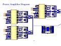
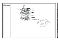
FILE No. 810-200603GR SERVICE MANUAL DVD HOME CINEMA THEATER SD-47HKSR The above model is classified as a green product (*1), as indicated by the underlined serial number. This Service Manual describes replacement parts for the green product. When repairing this green product, use the part(s) described in this manual and lead-free solder (*2). For (*1) and (*2), see the next page. JUL.,2006 GREEN (*1) GREEN PRODUCT PROCUREMENT The EC is actively promoting the WEEE & RoHS Directives that define standards for recycling and reuse of Waste Electrical and Electronic Equipment and for the Restriction of the use of certain Hazardous Substances. From July 1, 2006, the RoHS Directive will prohibit any marketing of new products containing the restricted substances. Increasing attention is given to issues related to the global environmental. Toshiba Corporation recognizes environmental protection as a key management tasks, and is doing its utmost to enhance and improve the quality and scope of its environmental activities. In line with this, Toshiba proactively promotes Green Procurement, and seeks to purchase and use products, parts and materials that have low environmental impacts. Green procurement of parts is not only confined to manufacture. The same green parts used in manufacture must also be used as replacement parts. (*2) LEAD-FREE SOLDER This product is manufactured using lead-free solder as a part of a movement within the consumer products industry at large to be environmentally responsible. Lead-free solder must be used in the servicing and repair of this product. WARNING This product is manufactured using lead free solder. DO NOT USE LEAD BASED SOLDER TO REPAIR THIS PRODUCT ! The melting temperature of lead-free solder is higher than that of leaded solder by 86°F to 104°F (30°C to 40°C). Use of a soldering iron designed for lead-based solders to repair product made with lead-free solder may result in damage to the component and or PCB being soldered. Great care should be made to ensure high-quality soldering when servicing this product especially when soldering large components, through-hole pins, and on PCBs as the level of heat required to melt lead-free solder is high. [CONTENTS] ❍ SECTION 1.GENERAL • SAFTY PRECAUTIONS ....................................................................................................... 1-2 • SPECIFICATION................................................................................................................... 1-3 ❍ SECTION 2. ELECTRICAL • TROUBLESHOOTING .......................................................................................................... 2-1 • OVERALL BOLCK DIAGRAM.............................................................................................. 2-2 • DVD SCHEMATIC DIAGRAM.............................................................................................. 2-3 • FRONT SCHEMATIC DIAGRAM......................................................................................... 2-4 • POWER AMPLIFIRE DIAGRAM........................................................................................... 2-5 • POWER SUPPLY DIAGRAM.................................................................................................... 2-6 ❍ SECTION 3. EXPLODED VIEW • EXPODED VIEW.................................................................................................................... 3-1 ❍ SECTION 4. PACKING VIEW................................................................................ 4-1 ❍ SECTION 5. REPLACEMENT PARTS LIST .......................................................... 5-1 - 1-1 - SECTION 1. GENERAL Safety Precautions WARN W A R NIINGS NGS The exclamation mark within a triangle is a warning sign alerting the user to important instructions accompanying the product. The lightning flash with arrowhead symbol within a triangle is a warning sign alerting the user to "dangerous voltage" inside the unit. To reduce the risk of electric shocks, do not remove the cover. No user-serviceable parts inside the unit. Refer all servicing to qualified personnel. This unit uses a laser. Only a qualified service person should remove the cover or attempt to service the player due to possible eye injury. Invisible laser radiation may occur when the unit is opened or interlocks are by-passed. Avoid exposure to laser beam. Use of controls, adjustments or procedures other than those specified herein may result in hazardous radiation exposure. This unit operates on 230V~50Hz. If it is not to be used for a long time, the AC power cord should be unpluged. The unit must not be exposed to moisture or rain. The unit should not be exposed to dripping or splashing and objects containing liquids, such as vases, should never be placed on top of it. The power switch for the unit is mounted on a secondary circuit and does not disconnect the whole unit from the mains in OFF position. Please ensure that all connections are properly made before operateing the unit. The unit should be positioned so that it is properly ventilated. Avoid placeing it, for example, close to curtains, on a carpet or inside a built-in fixture such as a bookcase. Openings for ventilation must not be blocked or covered during use. NOTE This product incorporates copyright protection technology that is protected by U.S. patents and other intellectual property rights. Use of this copyright protection technology must be authorized by Macrovision, and is intended for home and other limited viewing uses only unless otherwise authorized by Macrovision. Reverse engineering or disassembly is prohibited. Manufactured under licence from Dolby La boratories. " Dolby " and the double-D symbol are trademarks of Dolby Laboratories. Confidential Unpublished works. " 1992-1997 Dolby Laboratories, Inc. All rights reserved. CA U T ION Use of controls or adjustments or performance of procedures other than those specified herein may result in ha zardous radiation exposure. Do not open covers and do not repair yourself. Refer serviceing to qualified personnel. Th is DV D V I DEO player is class ified as a CLASS 1 LASER PR ODUC T as stated on the back of the set. Do not expose this unit to direct sunlight or heat sources. CA U T I ON: 1. Do not operate the system in an enclosed cabinet and allow about 10cm (4 inches) of free space all around the receiver for adequate ventilation. 2. No naked flame sources, such as lighted candles, should be placed on the apparatus. 3. Attention should be drawn to the environmental aspects of battery disposal. Following information is only for EU-member states: The use of the symbol indicates that this product may not be treated as household waste. By ensuring this product is disposed of correctly, you will help prevent potential negative consequences for the environment and human health, which could otherwise be caused by inappropriate waste handling of this product. For more detailed information about recycling of this product, please contact your local city office, your household waste disposal service or the shop where you purchased the product. - 1-2- Specification Technical data Power supply Power consumption Dimensions Laser Video signal-noise ratio Audio frequency range 220-240V mains voltage, 50Hz 120W ; In standby <3W 430W x 50H x 350D Semiconductor laser, wavelength 650 nm 55dB (DVD) DVD (PCM) 125Hz ~ 20kHz (+/- 3dB); CD 125Hz ~ 20kHz (+/- 3dB) FM tuner System Reception range Quartz-controlled PLL synthesiser system 87.5~108.00 MHz (50kHz increments) Audio output signal Audio L/R 2Vrms, 47kOhm Audio output Stereo 80W+80W (6 Ohms at 1kHz, THD 10%) Front: 80W+80W (6 Ohms at 1kHz, THD 10%) Center: 80W (6 Ohms at 1kHz, THD 10%) Rear: 80W+80W (6 Ohms at 1kHz, THD 10%) Subwoofer Headphones Ouptput: 80W (6 Ohms at 80Hz, THD 10%) Stereo output 3.5mm jack Front/Rear speakers Dimensions Impedance 92W x 140H x 100Dmm 6ohms Center speakers Dimensions Impendance 230W x 92H x 100Dmm 6 Ohms Subwoofer Dimensions Impedance 202W x 305H x 317Dmm 6 Ohms REFERENCE Surround Specifications subject to change without prior notice. 26 - 1-3- SECTION 2. ELECTRICAL Troubleshooting If you experience any of the following difficulties while using the system, use this troubleshooting guide to help you solve the problem. Should any problem persist, consult your nearest service center. • No power • Is the power cord firmly plugged into the power outlet? • One of the safety mechanisms may be operating. In this event, unplug the player from the power outlet briefly and then plug it in again. Severe hum or noise is heard • Check that the speakers and components are connected securely. • Check that the connecting cords are away from a transformer or motor, and at least 3 meters away from a TV set or fluorescent light. • Move your TV away from the audio components. • The plugs and jacks are dirty. Wipe them with a cloth slightly moistened with alcohol. • Clean the disc. No stereo sound effect when you play a Video CD or a CD • Set the Audio mode to STEREO. • Make sure you connect the system appropriately. The surround effect is difficult to hear when you are playing a Dolby Digital sound track • Check the speaker connections. • Depending on the DVD disc, the output signal may not be the entire 5.1 channel but monaural or stereo even if the sound track is recorded in Dolby Digital format. The picture noise appears • Clean the disc. • If video from this system has to go through your VCR to get to your TV, the copy-protection applied to some DVD programs could affect picture quality. If you still experience problems after checking your connections, please try connecting your DVD system directly to your TV’s input. The aspect ratio of the screen cannot be changed even though you set “TV TYPE” in the SETUP menu when you play a wide picture • The aspect ratio is fixed on your DVD disc. • Connect the system directly to the TV. Otherwise, you may not change the aspect ratio. • Depending on the TV, you may not change the aspect ratio. There is no sound or only a very low-level sound is heard • Check that the speakers and components are connected securely. • Make sure that you have selected the correct source on the system. • The protective device on the system has been activated because of a short circuit. Turn off the system, eliminate the short circuit problem and turn on the power again. • The audio connecting cord is damaged. Replace it with a new one. • The system is in pause mode or in slow-motion play mode, or fast forward or fast reverse is performed. Press /ll to • return to normal play mode. Check the speaker settings. The left and right sounds are unbalanced or reversed REFERENCE No picture • Check that the system is connected securely. • The video connecting cord is damaged. Replace it with a new one. • Make sure you connect the system to video input connector on the TV. • Make sure you turn on the TV. • Make sure you select the video input on the TV so that you can view the pictures from this system. • Make sure the TV SYSTEM and VIDEO output setting in the setup menu are set correctly. • Check that the speakers and components are connected correctly and securely. Adjust front balance parameter using SELECT and VOLUME+/-. The sound comes from the center speaker only • Depending on the disc, the sound may come from the center speaker only. No sound or only a very low-level sound is heard from the rear speakers • Adjust the speaker volume. The language for the subtitles cannot be changed when you play a DVD • Multilingual subtitles are not recorded on the DVD. • Changing the language for the subtitles is prohibited on the DVD. The subtitles cannot be turned off when you play a DVD • Depending on the DVD, you may not be able to turn the subtitles off. The angles cannot be changed when you play a DVD • Multi-angles are not recorded on the DVD. • Change the angles when the angle mark appears on the TV screen. The system does not operate properly • Static electricity, etc., may affect the system’s operation. Press ON/STANDBY button to turn off, then press again to turn on. - 2-1- 25 1 2 3 Overall Block Diagram 4 74ALS04 SPDIF IN CVBS D FLASH MBM29LV080BE-70NC SDRAM 4Mx16 D EEPROM 24C02 S-VIDEO DVD MOTOR Drive IC AM5888S LOADER M07P POWER BOARD VIDEO FILTER # Pb # Pr # SWITCH POWER SUNPLUS SPHE8281A (256) +5V +12V -12V AUX2 DX-8001 STA308A CS5340 CD4052 POWER AMPLIFIER FL FL FR FR C DDX-2100*2 STA508 * 3 C FL C FILTER 2CH AUDIO A/D SL SL SL SR SR SR SUB SUB SUB FM KEY ARRAY FR VFD HNA-11SM51T AUX1 AC1,AC2 B R/C CG/VS 52k Digital Audio Processor Bass and Treble Control 6CH Volume Control Bass management TP6311 VFD DRIVE AUDIO INPUT SELECT +34V C EXPAND I/O PORT 4094 MAIN BOARD SPEAKER OUT 光光光TUNER AM +5V PANNEL BOARD *SMC/SD/MS(PRO)/MMC/(CF) POWER PCB ASSY230V 150W SCART MPEG II Decoder DTS Decoder DOLBY DIGITAL Decoder DOLBY PROG LOGIC Decoder WMA Decoder MP3 Decoder TV ENCODE Progressive Scan u-com C B Y Line-out TUNER: KS0302 4558*3 APA3541 PHONES OUT PLL: LC72131M A RDS: LC72723 * Title TUNER BOARD Size A4 Date: File: 1 2 3 - 2-2- A Number SUNPLUS PROJECT 12-Dec-2005 E:\DR30H5\DR30H5.ddb Revision Sheet of Drawn By: 4 DVD Schematic Diagram LINE_MUTE1 LINE_MUTE1 DAGND DA3.3V C581 104 R525 47K R530 C582 104 4.7K R526 C590 102 C597 22UF NC Q501 C945 0 EAPD DAGND EAPD OUT1_A OUT1_B 64 63 62 61 60 59 58 57 56 55 54 53 52 51 50 49 OUT1_A OUT1_B R522 0 OHM 1 2 3 4 5 6 7 8 9 10 11 12 13 14 15 16 C579 104 DAGND 820PF XOPVIP1 XOPVIN1 XOPOP1 GND 102 R156 R157 102 C190 RF3.3V 68K 33K GND FCO RF3.3V RD7 RD6 RD5 RD4 RD3 RD2 RD1 C210 C211 104 GND 104 [CARD D1-D10] GND RD0 RWE ROE SPDCO SCO TRAYTRAY+ DMEA TRAYIN HOME R160 R161 2.2K 2.2K LDSW R100 4.7K R107 4.7K R106 4.7K RA9 RA10 +5 15 DOUT LRCK BICK OE 8 GND 11 12 13 14 7 6 5 4 Q8 Q7 Q6 Q5 Q4 Q3 Q2 Q1 4052-A 4052-B FAN_SW1 S-SWTCH S-BLNK DVD LINE_MUTE MUTE VCC1.8 reset VCC1.8 RF3.3V GND DVCC3 IC103 23 24 25 26 29 30 31 32 33 34 22 35 15 39 16 17 18 19 MA0 MA1 MA2 ENCODE1 ENCODE2 MA3 ENCODE1 ENCODE2 DVCC3 MA4 MA5 ST-LED EARDEC STB CARD_SENSE2 MA6 MA7 EARDEC MA8 MA9 MA3 MA2 MA1 MA10 MA11 DQM0 DQM1 GND MA0 MA10 VCC1.8 MWE M_CAS M_BA1 M_RAS DQM0 DQM1 MA4 M_CS0 FB920 FB921 FB922 FB923 M_CKE RAM_CLK M_BA0 MA5 MA6 MA7 MA8 MA9 M_CKE GND FB919 SRAM_CLK DVCC3 60 60 60 60 M_BA1 R168 C228 33 3PF MA11 37 38 20 21 VSSq VSSq VSSq VSSq D0 D1 D2 D3 RB107 33 1 2 3 4 8 7 6 5 C130 104 C905 103 C196 33PF C195 33PF I2C ADDR = 0XA0 DVCC R169 R151 R170 OPEN OPEN OPEN RWE RESET# GND R171 R140 R109 R108 C139 C136 C135 R167 R121 104 4.7K B5V Q107 OPEN 4.7k SD_VCC3 RA19 RA18 RA8 RA7 RA6 RA5 RA4 RA3 RA2 70A02 NC IC105 24C01/CAT24C021 GND DVCC3 GND 1 2 3 4 GND A0 A1 A2 GND 8 7 6 5 VCC WP SCL SDA 104 R163 100K R104 RA20 GND 33 NC 70A02 NC 4.7K C178 104 RESET# 27MHz XT101 10K NC R941 R144 R145 4.7K DVCC3 L901 3.3uH 33 33 I2C_CLK1 I2C_DATA1 I2C_CLK I2C_DATA GND GND C589 C591 C593 33pF 17 18 19 20 21 22 23 24 25 26 27 28 29 30 31 32 8 C846 R863 AGND 47PF NC 10K NC C844 102 4558 NC C816 2 R865 100K NC D11 D12 RB109 33 1 2 3 4 8 7 6 5 5.1K 1 2 3 4 33 MD3 8 7 6 5 MD4 8 X 3 Y 1K R829 16 150 C825 C841 ZD801 5.6V ZD802 5.6V +7V 100uF 104 -7V C842 C826 7 R856 -12V 100uF 150 104 4052-B 4052-A MD5 33 MD11 1 2 3 4 8 7 6 5 MD12 47K C839 101 L805 2.4uH R 7 AGND LINE OUT L 1 TU-L C829 10uF/16V C830 10uF/16V AGND LINE_R SCART IN_R C836 102pF NC C837 102pF NC LINE_R LINE_L LINE_L SCAR_L SCAR_R 1K 1K 6.8K NC R843 AGND MD6 MD7 RB110 2 TU-R L806 2.4uH MD9 D13 R847 TU-L MD10 D14 47K TU-R R833 R834 MD8 D15 AUX2 IN L 3 5.6K C835 102pF C838 5.6K 102pF AGND 4052-B 4052-A R 8 L804 2.4uH R845 R846 10 9 6 8 A B INH GND VEE AUX1 IN L 4 L803 2.4uH C833 102pF AGND C834 R841 5.6K 102pF AGND VDD R 9 5 L802 2.4uH 5.6K R839 12 1 14 5 15 2 11 4 X0 Y0 X1 Y1 X2 Y2 X3 Y3 AGND AGND MD2 RB108 6 L801 2.4uH 5.6K 4052 AGND 102 102 R855 +12V C848 104 D6 D7 D8 D9 D10 5.1K 10uF/16V 3 13 C849 C850 C818 L 1 1K R830 R828 R827 AGND IC804A AGND IC802 10uF/16V C817 JK801 RCA6 aux in&line out C831 102pF C832 102pF AGND AGND R C843 102 C813 C807 10uF/16V 100NF reset C824 104 C847 LINE_R 4.7K 5.6K +12VM R842 104 AINL Q803 CM5783 R837 R840 R814 24K C803 47pF +12V 10UF NC 100K 100K R826 9 RST LRCL R832 1K C827 10uF/16V IC803B 4558 SCAR_L SCAR_R SCART IN_R SCART IN_L SCART IN_L R844 6.8K NC MD13 MD14 MD15 GND SD_VCC3 SDRAM 64M-7 CN107 RA16 RA15 RA14 RA13 RA12 RA11 RA10 RA9 10PF R940 60 AGND R824 100K 100K R864 100K NC C815 AGND R823 R825 10 AINL SCLK A733 24K 7 6 MD0 MD8 MD9 Q106 FB924 7 C810 100uF IC804B 4558 NC 7 C808 104 LINE_MUTE1 47pF 6 5 R811 4.7K 5 AINR 11 VQ VD 150pF C821 R808 4.7K MD1 D4 D5 28 41 54 1 14 27 3 9 43 49 VSS VSS VSS VDD VDD VDD VDDq VDDq VDDq VDDq CKE CLK BA0 BA1 GND 2 4 5 7 8 10 11 13 42 44 45 47 48 50 51 53 36 40 D0 D1 D2 D3 D4 D5 D6 D7 D8 D9 D10 D11 D12 D13 D14 D15 NC NC/RFU A0 A1 A2 A3 A4 A5 A6 A7 A8 A9 A10/AP A11 LDQM UDQM WE CAS RAS CS 6 12 46 52 60 GND 0 6 12 AINR GND R809 C820 220pF R805 C804 R836 4.7K R806 4.7K R804 4.7K -12V VCC1.8 VCC1.8 R122 33 0 IC120 LM809 GND RF3.3V 4.7K 4.7K 4.7K 4.7K 104 B5V IR_IN VFDCLK VFDCE VFD-DA R103 R118 R178 R135 RF3.3V 5 10K NC DA3.3V 601 C814 100uF/16V AGND 13 VA C806 104 C812 1uF 14 REF_GND SDOUT 47PF NC 10UF NC C239/open GND 104 C580 AMCLK DOUT BICK LRCK 10K NC FLT+ MCLK VL AGND 33 R173 C133 R861 600 C805 104 AMCLK DOUT BICK LRCK 3 4 FB802 S-SWTCH S-BLNK DVD LINE_MUTE MUTE 10K 33 DA3.3V GND VCC1.8 GND 104 R815 4052-A 4052-B 1 2 3 4 5 6 7 8 9 10 11 12 13 IC102A RF3.3V 220pF R817 FB803 15 4.7K OUT8_A OUT8_B OUT8_A OUT8_B C845 R862 16 M1 GND 1 2 3 4 5 6 7 8 9 10 11 12 13 14 15 16 17 18 19 20 21 22 23 24 48 47 46 45 44 43 42 41 40 39 38 37 36 35 34 33 32 31 30 29 28 27 26 25 A16 BYTE# GND DQ15/A-1 DQ7 DQ14 DQ6 DQ13 DQ5 DQ12 DQ4 VCC DQ11 DQ3 DQ10 DQ2 DQ9 DQ1 DQ8 DQ0 OE# GND CE# A0 A15 A14 A13 A12 A11 A10 A9 A8 NC NC WE# RESET# NC NC RY/BY# A18 A17 A7 A6 A5 A4 A3 A2 A1 1 2 3 4 5 6 7 8 9 10 11 12 RA18 13 14 RA7 15 RA6 16 RA5 17 RA4 18 RA3 19 RA2 20 RA1 RA17 RA16 RA15 RA14 RA13 RA12 RA11 RA9 RA8 RWE RA0 RD7 RD6 RD5 SD_VCC3 RD4 C141 104 RD3 RD2 GND RD1 RD0 ROE A16 A15 A14 A13 A12 A11 A9 A8 WE# NC NC NC A18 A7 A6 A5 A4 A3 A2 A1 IC102 SST 40 39 38 37 36 35 34 33 32 31 30 29 28 27 26 25 24 23 22 21 A17 GND NC A19 A10 DQ7 DQ6 DQ5 DQ4 VCC VCC NC DQ3 DQ2 DQ1 DQ0 OE# GND CE# A0 RA17 RA19 RA10 RD7 RD6 RD5 RD4 TU-CE TU-DIN TU-CLK TU-GND 1.0mm*13Pin FCC SD_VCC3 FB124 FB125 FB101 FB128 FB102 FB129 R147 R158 R148 TU_12V TU-GND* RD3 RD2 RD1 RD0 FB103 R175 R119 TU-LED ST-LED R172 R625 1K TU-R 4094DA C954 104 C607 C955 100uF/16V OUT2_A OUT2_B OUT2_A OUT2_B 4094CK TU-DOUT RDS_CLK RDS_DATA 4.7K R601 4.7K R602 R604 4.7K 7.5K 2 C609 1 4.7K R606 47pF R618 C603 150pF 4.7K R605 4.7K R603 C601 220pF RDS_CLK RDS_DATA 3 R620 -12V OUT1_A OUT1_B OUT1_A OUT1_B R_CS1 RA0 SST39LF080/016 C710 GND R607 4.7K R608 R609 LINE_R R713 56K LINE_L R714 56K 10uF/16V R610 R611 5 IC701A 4558 4 10K 10uF/16V IC602B 4558 C606 47pF R614 7.5K C623 100uF/16V +12V C624 4.7uF/16V C614 104 C703 R628 4.7R R629 4.7R C616 104 C617 104 R615 4.7K 1 2 3 4 P_L P_R_OUT GND P_L_OUT P_L_CON 2.0mm*4pin EARDEC Q602 R617 CM5783 4.7K EARDEC AGND PH_MUTE PH_MUTE AGND AGND 3 R701 C622 220uF C612 10uF CN601 P_R 2.2 2.2 R627 DVCC 7 5 R626 10uH 10uH L601 L602 IC601 APA3541 + 1K C610 7 4.7K R612 1 10uF/16V 1 + C631 471 100K R621 6 C604 150pF C602 220pF 4.7K 4.7K 30K 2 101 C630 471 - 47PF R715 C702 C619 R623 7.5K C701 LINE_R LINE_L 47pF R619 101 C625 220uF/16V - 3 100K C618 6 AGND 4.7K AGND 1K R622 C613 104 C608 4.7K R624 100K C611 10uF 10uF/16V IC602A 4558 R613 7.5K C605 47pF ROE R_CS1 RA1 Q601 CM5783 10 R630 +12V 10 TU-L 4094CK TU-DOUT 601 1K 1K TU12V +12V TU-L TU-R 4094DA AGND GND MXIC 29LV040/SST39VF040 TU-LED ST-LED 600 NC 600 TU12V 601 600 601 600 33 33 33 C627 C186 GND C188 16 BICK AGND NC CS5340 M0 C629 R153 470K TCO IC101 SPCA8281AL 256 pin share DVCC 10 9 2 C628 RFCT 0.047UF QS QS 33 104 103 C193 RA5 RA6 RA7 RA8 CLK D STR 3 2 1 4094CK 4094DA 4094STR 4094CK 4094DA 4094STR DOUT LRCK 10K R819 AGND IC801 1 R816 102 0.22UF C155 C811 104 C809 100uF 4094 NC 600 AGND IC104 AGND 102 C187 102 C192 C189 300PF 331 R818 DA3.3V C140 104 GND R822 10K FB804 1 2 3 4 2.0mm*4pin 102 10K C626 103 T104 RFCT C191 C925 GND 47K NC 47K NC 8.2K 8.2K 8.2K 8.2K 8.2K 8.2K C154 104 DVCC3 EARDEC 104 104 LINE_L Q802 CM5783 R820 10uF 47UF GND VCC1.8 4.7K 1K Q801 R849 R850 R857 R858 R851 R852 R853 R854 47UF 104 33K (1%) R821 CN108 C924 104 R838 R831 -12V C823 104 C621 + C183+ C124 C185 C126 R162 GND 75 DVCC 104 C127 AIN_R C128 ATO AIN_L RA1 RA2 RA3 RA4 C828 10uF/16V 1 IC803A 4558 C615 APC3.3V RF3.3V VREF1 VREF2 192 191 190 189 188 187 186 185 184 183 182 181 180 179 178 177 176 175 174 173 172 171 170 169 168 167 166 165 164 163 162 161 160 159 158 157 156 155 154 153 152 151 150 149 148 147 146 145 144 143 142 141 140 139 138 137 136 135 134 133 132 131 130 129 24K 2 R813 24K 100UF16V C120 VSS_ADA VDD_ADA VM AIN_R ATO AIN/AIN_L R_A1 R_A2 R_A3 R_A4 E_VDD_K1 R_A5 R_A6 R_A7 R_A8 E_VDD_O2 R_A9 R_A10 M_A12/GPIO M_CS1_B/GPIO GPIO/M_D16 GPIO/M_D17 VSS_O5/VSS_K5 GPIO/M_D18 GPIO/M_D19 GPIO/M_D20 GPIO/M_D21 GPIO/M_D22 GPIO/M_D23 VDD_K4 M_DQM2/GPIO M_DQM3/GPIO GPIO/M_D24/R_D8 GPIO/M_D25/R_D9 GPIO/M_D26/R_D10 GPIO/M_D27/R_D11 VDD_O4 GPIO/M_D28/R_D12 GPIO/M_D29/R_D13 GPIO/M_D30/R_D14 GPIO/M_D31/R_D15 M_A3/R_A3 M_A2/R_A2 M_A1/R_A1 VSS_O4/VSS_K4 M_A0/R_A0 M_A10/R_A10 M_BA1/GPIO M_DQM0/GPIO M_DQM1/GPIO M_A4/R_A4 VDD_K3 M_A5/R_A5 M_A6/R_A6 M_A7/R_A7 M_A8/R_A8 M_A9/R_A9 M_CKE/GPIO VSS_O3/VSS_K3 M_CLKO VDD_O3 M_A11/GPIO M_D8/R_A11 M_D9/R_A12 R835 R810 4.7K C802 47pF R807 4.7K C620 DVDLDO CDLDO DVDMDI R803 4.7K VGND 104 GND C166 R812 4.7K 3 C418 101 8 F E 10PF C822 150pF ZD601 5.6V CDB CDA RFIP RFIS RFSUM DPDA DPDB DPDC DPDD DVDD DVDC DVDB DVDA CDB CDA CDF CDE RF_AVSS APC_AVSS DVDLDO CDLDO DVDMDI CDMDI APC_AVDD SRV_AVDD V21 R33K V165 SVOTST RFRPPH RFRPBH RFRPMEAN SBADPH SBAD FEO TEO TEOLP OPVIP OPVIN OPVOP SRV_AD_AVSS VRGD AD_DA_VDD DA_TEO DA_FEO DA_VSS E_VDD_O0 R_D7 R_D6 R_D5 R_D4 R_D3 R_D2 R_D1 E_VSS R_D0 R_WE_B R_OE_B SPDC_OUT/GPIO SC_OUT/GPIO SC1_OUT/GPIO TRAY_OUT/GPIO DMEA/GPIO FGIN/GPIO HOMESW/GPIO LDSW/GPIO C819 220pF 4 DPDC T117 CDB T101 CDA 1 2 3 4 5 6 7 8 9 10 11 12 13 14 15 16 17 18 19 20 21 22 23 24 25 26 27 28 29 30 31 32 33 34 35 36 37 38 39 40 41 42 43 44 45 46 47 48 49 50 51 52 53 54 55 56 57 58 59 60 61 62 63 64 DPDA D C B A R802 4.7K 4 681 R801 4.7K OUT7_A OUT7_B OUT7_A OUT7_B CVBS1 101 101 101 101 101 101 101 101 101 101 104 104 681 C163 R412 1UH 10 RAM_CLK 681 681 C162 AGCOP AGCON FLTIN FLTIP RFO RFRP AGCCAP GMRES RF_AVDD DS_AVDD SLVL CNIN RFI PLL_DS_AVSS LGIN LPFNIN FDFLT PDFLT VREFO LPFN LPFO PLL_AVDD E_VDD_O3 E_MX38 E_MX37 E_MX36 E_MX35 E_MX34 E_MX33 E_MX32 E_MX31 R_A0 E_VSS NC VSS_TVA2 TV_DAC5 VDD_TVA2 TV_DAC4 TV_DAC3 VSS_TVA1 VDD_TVA1 TV_DAC2 TV_DAC1 VSS_TVA0 VDD_TVA0 TV_DAC0 V_REFOUT V_FSADJ V_BIAS V_COMP UA0_TX/GPIO UA0_RX/GPIO A_XCK/GPIO A_BCK/GPIO VSS_K6/VSS_O6 A_LRCK/GPIO AUD3/GPIO AUD2/GPIO AUD1/GPIO VDD_O5 AUD0/GPIO IECTX/GPIO IECRX/GPIO AUD4/GPIO C161 C160 GND DAGND VGND C413 101 R150 DVCC3 DFCT/GPIO VDD_K1 GPIO/TRAY_IS_IN GPIO/TRAY_IS_OUT GPIO/ttio0_4 VSS_O1/VSS_K1 GPIO/ttio1_5 GPIO/ttio2_6 GPIO/ttio3_7 VDD_O1 GPIO R_CS4_B/GPIO R_CS3_B/GPIO R_CS2_B/GPIO R_CS1_B/GPIO RST_B IR_IN/GPIO VFD_CLK/GPIO VFD_STB/GPIO VFD_DATA/GPIO R_A20 R_A19 R_A18 R_A17 R_A16 E_VDD_K0 R_A15 R_A14 R_A13 R_A12 R_A11 E_VDD_O1 CLKIN CLKOUT USB_GND USB_VDD USB_DP USB_DM VSS_PLLA VDD_PLLA VSS_PLLV VDD_PLLV M_D7/R_D7 M_D6/R_D6 M_D5/R_D5 M_D4/R_D4 M_D3/R_D3 VDD_O2 M_D2/R_D2 M_D1/R_D1 M_D0/R_D0 M_WE_B/R_WE_B M_CAS_B/R_OE_B M_RAS_B/R_A20 VSS_O2 M_CS0_B/GPIO M_BA0/R_A19 M_D15/R_A18 M_D14/R_A17 M_D13/R_A16 VDD_K2 M_D12/R_A15 M_D11/R_A14 M_D10/R_A13 NC(120PF) 1UF FB502 601 DA_PLLGND C417 101 C406 3906 NC GND C596 101 10PF L406 0 OHM Q406 101 C595 122 Y_O C911 100uF/16V C840 101 R920 TV_DAC0 CARD_D7 C966 1UH C412 101 75(0805) NC V+5V SPDIFIN 65 66 67 68 69 70 71 72 73 74 75 76 77 TRAYOUT 78 R_CS1 79 RESET# 80 IR_IN 81 VFDCLK 82 VFDCE 83 VFD-DA 84 RA0 85 RA19 86 RA18 87 RA17 88 RA16 89 90 RA15 91 RA14 92 RA13 93 RA12 94 RA11 95 96 CLKIN 97 CLKOUT 98 99 USB_PLL3.3 100 USB_DP 101 USB_DM 102 103 APLLVCC3.3 104 105 106 MD7 107 MD6 108 MD5 109 MD4 110 MD3 111 112 MD2 113 MD1 114 MD0 115 MWE 116 M_CAS 117 M_RAS 118 119 M_CS0 120 M_BA0 121 MD15 122 MD14 123 MD13 124 125 MD12 126 MD11 127 MD10 128 C147 C148 C405 +12VM R932 1K Q905 2sc2878 C929 220uF/16V R848 SPDIFOUT RFIP PUHRF L405 75(0805) Q405 3906 R411 82 R406 Q904 2S733 R933 1M FB501 601 C586 104 2 SPDIFOUT SPDIFIN 1UF DVCC3 T116 RFIP R405 FAN_SW DA3.3V R529 3.3K C592 220pF VGND V+5V TV_DAC1 GND +12V 104 33 33 100uF VGND R134 R137 C416 101 8 C149 C583 AMCLK OUT7_A OUT7_B OUT8_A OUT8_B 10K R528 RESET# I2C_DATA1 I2C_CLK1 AMCLK RESET# Cr_O 10PF OUT6_A OUT6_B OUT7_A OUT7_B OUT8_A OUT8_B 8 GND 1UF OUT6_A OUT6_B 10K R527 DA3.3V 1UH C411 101 R410 82 AMCLK BICK LRCK SD2 SD1 SD0 DVCC3 256 255 254 253 252 RFO 251 RFRP 250 C112 104 249 248 PLLVCC3.3 247 R136 2.2 246 245 244 RFI 243 242 LGIN 241 FD 240 PD 239 Vref0 238 237 236 235 4.7K 234 R149 233 4094CK 232 4094DA 231 4094STR 230 TU-DOUT 229 I2C_DATA1 228 I2C_CLK1 227 RDS_CLK 226 RDS_DATA 225 RA20 224 223 222 221 TV_DAC5 220 219 TV_DAC4 218 TV_DAC3 217 216 215 TV_DAC2 214 TV_DAC1 213 212 211 TV_DAC0 104 210 V_REF R143 209 V_FSADJ 390 208 V_BIAS 104 207 V_COMP C119 206 V_V_SYNC 104 205 V_H_SYNC 204 BICK 203 202 LRCK 201 200 SD2 199 SD1 198 197 SD0 196 195 194 193 C151 C404 Q404 3906 DA3.3V 100uF 33 AMCLK T115 RFRP GND TV_DAC2 C588 104 DAGND VGND L404 75(0805) V+5V V_H_SYNC R117 C118 C117 4094CK 4094DA 4094STR VGND VVCC3 C415 101 C410 101 R409 75 R404 V_V_SYNC OUT3_A OUT3_B OUT4_A OUT4_B OUT5_A OUT5_B DAGND 4 R B T102 T103 OUT3_A OUT3_B OUT4_A OUT4_B OUT5_A OUT5_B 4 G V_V_SYNC V_H_SYNC DAGND 10PF C594 C C403 Q403 3906 DVCC3 C115 104 RFI RFO C159 681 C156 101 R127 20K R131 1.2K (1%) C153 103 Y TV_DAC3 DA3.3V C587 104 G/Y_O C584 CVB L403 1UH 75(0805) C585 FD 5.1K 5.1K GND VGND V+5V C CVB Y X R403 C414 101 102 B/U_O 10PF C409 101 104 47PF Cr Cb (S-Video) (S-Video) 1.5K RF3.3V X Y C402 R408 75 C600 VGND L402 1UH 75(0805) Q402 3906 R143 full 390 ( 1/2 680) C598 10uF/16V 48 47 46 45 44 43 42 41 40 39 38 37 36 35 34 33 OUT2_A OUT2_B VDD2.5_5 GND_5 VDD3.3_5 OUT3_A OUT3_B OUT4_A OUT4_B OUT5_A OUT5_B VDD2.5_4 GND_4 VDD3.3_4 OUT6_A OUT6_B 104 47PF C158 R129 R130 CVB C Y TV5 220 IC504 STA308A OUT2_A OUT2_B DAGND 22uF/16V C157 Vref0 PD CVB R916 R919 0.068UF NC 4.7K 4.7K 1UF R128 C152 NC C164 RDS_CLK RDS_DATA C150 GND LGIN R132 TV_DAC4 TV1 TV2 TV3 TV4 R524 MVO TEST_MODE VDD3.3_1 GND_1 VDD2.5_1 SDI_78 SDI_56 SDI_34 SDI_12 LRCKI BICKI VDD3.3_2 GND_2 VDD2.5_2 RESET PLL_BYPASS C169 C170 C171 C172 C173 C174 C175 C176 C177 C145 C129 C180 TV0 33 NC DA3.3V C599 C407 101 R407 75 R402 V+5V 1/2 current config R/V_O B/U_O G/Y_O Cr_O Y_O CVBS1 C408 101 C632 R/V_O 10PF 33 C401 33 L401 1UH 75(0805) Q401 3906 33 R401 V+5V TV_DAC5 R523 DOUT SD2 SD1 SD0 LRCK BICK DOUT SD2 SD1 SD0 LRCK BICK SA SDA SCL XTI PLL_FILTER VDDA_PLL GNDA_PLL VDD3.3_PLL CKOUT VDD2.5_3 GND_3 VDD3.3_3 OUT8_B OUT8_A OUT7_B OUT7_A DA3.3V PWDN SDO_78 SDO_56 VDD2.5_7 GND_7 VDD3.3_7 SDO_34 SDO_12 LRCKO BICKO VDD2.5_6 GND_6 VDD3.3_6 EAPD OUT1_A OUT1_B OUT2_A OUT2_B 10uF/16V C705 SB2A NC 104 +5V_P AGND B5V D908 IN5401 BOTTOM CONTACT FOCFOC+ RAD+ RAD- IC106 AM5869 LDOV33+ 14 FOC+ PUHRF 13 FOCA B F R123 Q104 3904 LDOV33+ 3 LDOV18- VVCC3 ZD702 FB C713 RF3.3V C949 104 GND XOPVIN1 SP+SNSR DA3.3V C958 220UF C950 220UF C959GND 104 RF3.3V BIAS SP+ SP- R133 R120 0 12 0 11 CTKerr1 CTKerr2 VOSP+ TCO 27 VREF2 25 LDOV18+ LDOV18+ C134 104 LDOV18- BIAS + - VINSP 10K 4 3.3 OHM/1W 4K7 R903 10K C103 C104 C105 VGND 104 104 104 C914 104 2 1 SPDCO 18 DMEA 28 VOSL+ - 10K VINSL C131 100UF16V 104 C132 104 23 SCO 33 33 33 33 33 FB106 FB107 5 4 3 2 1 C230 C231 FB108 600 LOAD+ 9 10 VOLD- FWD C110 C111 C113 C114 104 104 104 104 TrayDriver Pre-Driver REV VOLD+ TRAY+ 7 30 600 FB917 D910 GND +12V_P GND FB918 600 1 2 3 4 5 C137 104 GND 1N4148 /FB +5V_P C709 104 AGND DVCC setup dvd disc s-video/rgb 4:3/16:9 SWTCH R413 +12V GND C121 104 C934 220UF C935 100UF C915 104 C916 104 VGND GND 561 AC1 AC2 -27V GND B5V* FB903 -27V GND 1206 100V R936 ZD901 12V 600OHM/1W C906 104 R911 33 NC 10-12V GND scart 8pin 16:9 4:3 10-12V aux&tuner &stand by scart 8pin 4:3/16:9 no 0 S-SWTCH S-SWTCH DVD DVD Q407 MC5783 R418 GND 4.7K R415 GND 10K JK401 CVBS1 Y_O Cr_O FB411 FB412 FB413 100 100 100 D901 1N4148 D902 1N4148 SPDIFIN C207 LINE_MUTE1 PH_MUTE I2C_CLK* 1N4148 D903 C927 101 LINE_MUTE 33 NC 33 NC 1N4148 R906 R139 R908 R909 R910 R937 R938 33 OHM VFD-DA 33 OHM VFDCLK 33 OHM VFDCE 33 OHM ENCODE1 33 OHM ENCODE2 4.7K 4.7K 1N4148 R202 R931 Q906 2S733 PO_MUTE R939 100K NC V+5V VFD-DA VFDCLK VFDCE ENCODE1 ENCODE2 R902 DVCC IC116 Q903 CM5783 NC GND 7 DVCC 9 B5V 12 DVCC C956 104 R921 R914 0 VCC GND A/B G 1 15 R211 10K R201 104 R212 C968 101 GND R207 10K 10K 15 2 1 4 3 5 6 RCA+SVIDEO GND IC201 74HC04 33 C206 33 GND IR_IN 16 8 1Y 2Y 3Y 4Y SN74LVC157APW 2 1A 3 1B 5 2A 6 2B 11 3A 10 3B 14 4A 13 4B 4052-A 10K IR_IN 33 1N4001 RF_5VNC C951 220UF/10V R917 10K NC DVCC R905 100K NC 600 GND MUTE 1N4001 D907 Text C967 101 C201 104 200 100 LINE_MUTE MUTE D911 I2C_DATA I2C_CLK R159 R138 D906 R918 C433 15 GND 104 R924 PH_MUTE D904 1K IR C432 15 VGND LINE_MUTE1 C923 104 STANDBY I2C_DATA* C431 -12V B5V IR VFD-DA* VFDCLK* VFDCE* ENCODE1* ENCODE2* VGND 5.6V Q409 CM5783 10-12V R930 600 OHM/1W 600 ST_MUTE FB909 5-7V 16:9 1K CON7 C910 100uF/16V C947 104 11Pin 2.0mm 16:9 CVBS1 Y_O Cr_O 4 11 10 9 8 7 6 5 4 3 2 1 4:3 16:9 4:3 C909 100uF/16V GND CN302 0/1-3V 4:3 scart 8pin 7 6 5 4 3 2 1 BLNK R/V_O R/V_O DVCC voltage scart 8pin scart 8pin C913 220U/16V +12V C928 104 GND - 2-3- 2K B/U_O G/Y_O B/U_O G/Y_O R416 Q408 75 CM5783 R417 GND 561 5Pin 2.0mm GND CN401 CVBS1 CVBS1 S-BLNK R414 GND GND FB901 600 -27V GND CN303 C138 104 C912 104 1 2 3 4 5 CON5 AGND 600 FB905 C907 104 C908 220uF C918 104 SCA_L SCA_R 10uF SCAR_R SCAR_L R727 2K 24K 4.7K NC 220uF C921 TRAY- 8 19 C229 220UF16V R726 FAN_SW1 FAN_SW STANDBY 1 2 3 4 5 6 7 8 9 10 10Pin 2.54mm C920 MVCC Vcc1 Vcc2 AGND +12V 104 CN402 C430 10uF C429 SCAR_R SCAR_L 4.7K scart 16pin B5V R934 33 MVCC 6 TRAYIN AT5660 33 5PIN 2.0mm LOAD- 2sc2878 SCART IN_L SCART IN_R SCART IN_L SCART IN_R Q108 2S733 R708 33 Q702 2sc2878 1K ZD406 R923 STB CN902 0 LOADLOAD+ TRAYOUT Q703 R721 C704 10uF/16V V+5V GND GND R176 21 R707 100K C707 FAN RF_5V C961 C962 C963 C964 C960 104 104 104 104 104 15K VCTL 2 1 2.54mm*2Pin 600 FB906 + BIAS + Driver VOSL- STBY 68(1/2W) S-BLNK 2.2 C904 SLED+ 2K 68(1/2W) AGND C919 GND 600 600 600 1N4148 C706 104 R901 C922 HOME SLEDSLED+ 17 R724 (R0805) DAGND VCC1.8 SLED- R720 C9021206 100V 104 3.96MM 25K SPSP+ R703 10K 4558 IC701B D703 600 +27V FB910 CN901 SD_VCC3 C168 C903 220UF ZD701 7V NC AGND C901 C234 C235 C236 C237 C238 600 600 600 R716 C711 220K 0.001uF 7 Text 5 GND GND VCC1.8 +12V_P ZD703 8.5V-8.9V NC R725 2K 104 C116 104 Ic>1.5A SS8550(DIP EBC) 加加加加加 Q901 R904 AGND R728 68K 6 VVCC3 C165 100UF R907 GND Driver VOSP- 26 24 GND 600 600 FB121 FB122 FB123 FB105 C232 C125 C184 R165 150K FB109 FB120 GND CN103 CDLDO VINTK 10K 7.5K 104 104 104 C917 104 JST-CON6-2 33 GND GND R116 0 + X2 VNFTK 472 33 5.1 D102 1N4148 104 R152 GND DVDLDO Q105 2SB1132 47UF C182 C123 R142 D101 1N4148 0 PUH_CDLD PUH_DVDLD 5.1 47UF Q100 2SB1132 R115 Driver VOTK- R718 C109 104 R155 470K C227 6 5 4 3 2 1 20 1 PreGND LDSW G 100K CN102 GND VOTK+ 7.5K R164 22 R124 XOPOP1 + 16 R166 150K 470K C108 C107 104 R154 APC3.3V + 15 472 VREF2 GND2 R126 470 XOPVIP1 APC3.3V RAD+ RAD- + C226 GND GND1 S S R702 2K DVCC3 DVCC3 C106 C948 220UF CN701 470pF 4.5V SD_VCC3 FB FB NC 104 100K Q103 2SK3018 104 C167 2 FB908 FB916 DAGND 29 Q102 2SK3018 D D 10UH GND C122 CFCerr1 7.5K CFCerr2 C233 CD_VR DVD_VR 0 0 C142 104 100UF X2 33 R112 R113 L101 R114 0 BIAS VNFFC +3.3V 20K L102 10UH + 5 LDOV33- 470 20K R912 12K FCO + 7.5K R125 104 1 FB FB SS8550(DIP EBC) Q902 R915 C938 C939 C940 C941 C942 C943 C944 C945 C946 C101 FB915 FB907 Ic>1.5A 0.5 OHM/1W 68PF 68PF 68PF 68PF 68PF 33pF 68PF 68PF 68PF 104 PUH_DVDLD# RF3.3V VOFC- VINFC 10K RF_5V GND C102 E 0.5mm*24Pin + VREF1 CDVR DVD_VR# PUH_CDLD# DVDMDI LDOV33- VOFC+ Driver FB914 R913 DIP28-SSOPH 20K C D G 1 2 3 4 5 6 7 8 9 10 11 12 13 14 15 16 17 18 19 20 21 22 23 24 104 FF+ T+ TC D CD/DVD SW RF A B F GND VC(Vref) VCC E NC CD-VR DVD-VR CD-LD MPD HFM-VCC NC DVD-LD LD-GND 14 13 12 11 R203 10 9 8 1 2 3 R213 33 NC 4 5 6 R208 33 NC 7 R205 R214 33 R922 DVCC C204 104 R206 33 C202 JK201B COAX L201 2.4uH 104 4 IN 10K R204 33 R210 75 C203 104 10K 10K 5 2.4 uH FB 1206 CN104 -12V 8 D909 7 D905 8 600 FB904 1 MVCC C197 10UF C205 104 C208 101 GND JK201A 1 2 GND R209 75 NC C209 101 3 OUT OPT IN L202 2.4uH Front Schematic Diagram ZD301R301 5.6V 1K R302 1K R305 22K JK601 15 14 13 12 11 10 9 8 7 6 5 4 3 2 1 19 18 17 16 39 38 37 36 35 34 33 32 31 30 29 28 27 26 25 24 23 22 21 20 DP301 RB303 AC1 AC2 -27V GND B5V 1 2 3 4 5 RB601 5 4 3 2 1 FB602 FB601 EARPHONE C632 C635 104 102 4 3 2 1 600 600 C633 4Pin 2.0mm C634 102 AGND 104 GND 7Pin 2.0mm SN301 C307 104 C308 104 C311 100UF RB302 R322 10K 1N4148 NC D304 1N4148 NC DIN R323 R324 D305 D306 TA303 TA305 TA302 TA304 TA306 TA307 4.7K 4.7K 1 3 R312 R313 C318 LED4 STANDBY R304 10K NC R314 10K NC B5V R319 1K NC 1N4148 1N4148 3Pin 2.0mm 100 100 100 4.7K R328 TA301 DOUT R327 0 10K 10K 10K 10K VR301 2 VR3D ENCODE1 100P R311 R309 R310 R326 DIN R325 C309 C312 DOUT R315 R316 R317 R318 104 100UF 0 NC 0 NC 3Pin 2.0mm 100P ENCODE2 1 2 3 1 2 3 C310 104 NC RB304B 1 D301 151 NC LM809 NC RB304A 4.7K NC 1N4148 NC C306 R306 100K NC C304 102 NC 3 4.7K NC D303 455K NC C305 151 NC IC302 15P 1N4148 NC C317 2 56K C313 D302 11Pin 2.0mm C315 13 12 11 10 9 8 7 6 5 4 3 2 1 10K NC R329 C316 221 R308 560 NC R321 XL301 11 10 9 8 7 6 5 4 3 2 1 I2C_DATA I2C_CLK ST_MUTE IR VFD-DA VFDCLK VFDCE ENCODE1 ENCODE2 R303 0 NC B5V PSW LED4 15P K4 K3 K2 K1 STB CLK IIC_SCL IIC_SDA DIN/OUT REMOTE MODE RESET OSC1 40 41 42 43 44 45 46 47 48 49 50 51 52 15P GR5 GR4 GR3 GR2 GR1 VDD PSW LED4 LED3 LED2 LED1 GND OSC2 SG12 SG11/KS11 SG10/KS10 SG9/KS9 SG8/KS8 IC301 SG7/KS7 SG6/KS6 VDTR63111 SG5/KS5 (VDTR6311A/PT6311) SG4/KS4 SG3/KS3 SG2/KS2 SG1/KS1 VDD C314 SG13 SG14 SG15 SG16 SG17/GR12 SG18/GR11 VDD VEE SG19/GR10 SG20/GR9 GR8 GR7 GR6 10 OHM 26 25 24 23 22 21 20 19 18 17 16 15 14 STANDBY 3 2 1 27 28 29 30 31 32 33 34 35 36 37 38 39 C932 C319 33P - 2-4- Q301 A733 NC R320 1K RB301A 4 3 2 1 4Pin 2.0mm C320 33P RB301B 4 3 2 1 4Pin 2.0mm TA308 LD301 29 28 C503 104 27 DAGND 26 EAPD R501 10K EAPD 25 24 DA3.3V 23 22 C504 104 C505 104 21 20 19 PGND2N INRA PGND2P INLB VCC2P INLA OUTPR TWARN OUTPR FAULT OUTNL TRI-STATE OUTNL PWRDN VCC1N CONFIG PGND1N VL PGND1P VREG1 VCC1P VREG1 OUTPL GNDR1 GNDREF OUTPL NC 3 +34V 4 5 6 DAGND C546 1UF C555 471 29 OUT3_A C511 DAGND 104 9 28 26 EAPD R503 10K EAPD L502 30uH 0 104 R505 C518 104 25 24 DAGND C517 27 DAGND DA3.3V 1 L513 INDUCTOR4 2 23 3 4 22 L- L+ C534 104 C535 104 21 20 10 11 C552 +34V 1000UF 12 13 14 3 1 L503 30uH C556 471 1UF DAGND C547 19 C519 104 R506 2 C520 104 C521 104 4 R+ PGND2N INRA PGND2P INLB VCC2P 5 6 TWARN OUTPR FAULT OUTNL TRI-STATE OUTNL PWRDN VCC1N CONFIG PGND1N VL PGND1P 8 VREG1 OUTPL GNDR1 OUTPL C550 1UF C539 104 DAGND C540 R520 15 OHM C536 DAGND 104 9 11 12 13 14 0 L510 30uH 104 R513 C541 104 L511 30uH C554 +34V 1000UF C560 471 16 0 1UF DAGND C551 C542 104 R514 C543 104 C544 104 C537DAGND 104 17 0 L512 30uH R515 C545 104 18 DAGND L514 INDUCTOR4 C512DAGND 104 17 0 R507 L504 30uH C522 104 18 DAGND 28 C508 104 27 DAGND 26 EAPD R502 10K EAPD 25 24 DA3.3V 23 22 C509 104 C510 104 21 20 19 OUTPR FAULT OUTNL TRI-STATE OUTNL PWRDN VCC1N CONFIG PGND1N VL PGND1P VREG1 VCC1P VREG1 OUTPL GNDR1 OUTPL GNDREF NC C513 DAGND 104 9 L506 30uH 0 R509 1 L515 INDUCTOR4 C526 104 L- R+ 3 R- SR- 2 4 SR+ 1 3 C- 4 C+ JK501 102 102 102 102 102 102 102 102 102 102 102 102 10 11 C553 +34V 1000UF 12 13 14 16 C558 471 1UF DAGND C549 C514DAGND 104 0 C527 104 R510 DAGND 2 C528 104 C529 104 L516 INDUCTOR4 DAGND R519 15 OHM 15 17 L507 30uH 0 L508 30uH R511 C530 104 18 DAGND - 2-5- C577 TWARN 8 104 C- L+ C578 OUTPR R518 15 OHM 7 C525 SR- C+ C575 INLA DAGND SR+ C576 VCC2P DAGND C524 104 SL- C573 INLB 6 C557 471 SUB- SL+ C574 PGND2P C548 1UF SUB+ C572 INRA 5 C563 PGND2N C571 29 INRB +34V 4 C570 OUT5_A VCC2N C523 104 R508 0 C569 30 VREG2 3 C568 OUT5_B OUTNR L505 30uH 0.68UF 31 VREG2 DAGND C567 OUT5_A OUT4_A OUTNR C564 OUT5_B 32 VSIG 1 2 + OUT4_A OUT4_B GNDS 0.68UF 33 DAGND OUT4_B 34 DDX2060 + C506 104 C507 104 35 VSIG + IC502 36 L517 INDUCTOR4 3 SUB- 2 4 SUB+ 1 3 SL- 4 SL+ 1 2 DAGND R521 15 OHM 15 NC GNDREF DAGND 10 VCC1P VREG1 C559 471 7 OUTPR INLA R512 0 +34V DAGND R517 15 OHM 15 16 0 R- INRB C538 104 3 4 VCC2N VREG2 L509 30uH C565 30 OUTNR DAGND 0.68UF OUT3_B C533 104 C515 104 R504 0 C516 104 R516 15 OHM 7 8 31 L501 30uH C561 VCC2N INRB OUT6_A VREG2 1 2 C566 OUT2_A VREG2 OUTNR 32 OUTNR 0.68UF 30 VREG2 DAGND 2 0.68UF 31 OUT2_B OUTNR C562 OUT2_A OUT1_A GNDS VSIG 0.68UF OUT2_B 32 OUT1_B VSIG + OUT1_A 34 33 DAGND OUT1_B 35 OUT3_A + C502 104 C501 104 1 + 36 OUT3_B DDX2060 OUT6_B GNDS VSIG + OUT6_A 34 33 DAGND OUT6_B 35 VSIG + C531 104 C532 104 IC501 DDX2060 IC503 36 + Power Amplifier Diagram L518 INDUCTOR4 • Power supply diagram D3 R6 C4 5.1K 1% 10uF/50V 13 180K R2 10K RJ2 82K R4 4.7K 1% R11 R3 56K 1N4148 DW3 GND +34V C2 222K 36V/0.5W 16V/0.5W DW9 C5 22uF/25V RN 10K 100K IC1 TL494 16 GND R13 3.9K R15 1K R14 1K GND 8 GND 7 9 10 1815 D8 T5 TR3 ! D4 UF4004 1 4 L3 RB13 10R 1N5822 102 IC3A C48 4.7uF/50V ! C21 D20 UF4007 EL817 - 2-6- C34 472 RB18 5.1R 3.96 2 3 4 5 6 7 8 9 10 GND RB15 RB14 1.5K 1K Q3 C31 104 C40 104 GND L2 C32 C50 104 GND RB12 1815 1.5K C30 104 GND 220uF/25V D28 +12V GND PCON D26 SB260 RB20 1K C35 2200uF/10V C36 1000uF/10V RB2 330R ST+5V GND ! RB1 1K IC3B EL817 C24 104 IC4 TL431 RB5 10.4K 1% RB3 1K RB4 GND 10K 1% +5V C20 DW8 3.3V/0.5W D25 RA3 100K/2W Q2 MCR100-8 2 Q4 5551 C27 C38 HV DW2 27V/0.5W D22 UF4004 220uF/25V C25 102 CN2 470uF/16V RB25 100R C51 0.47uF/100V C19 22uF/50V 3 10K C33 104/100V RB10 24K D27 1N4148 Q5 MJE702 RB16 RB17 1K 62K 1% R9 AC1 DW4 3.3V/0.5W 1 AC2 D21 UF4004 10R GND DW5 5.1V/0.5W R7 C6 104 RB11 5.6K 5.1R RB8 1K 1K 3.9K 1% C22 104 C29 RB6 R28 GND AC1 AC2 -29V GND +12V GND +5V ST+5V PCON -29V 220uF/35V GND RA4 R10 8.2K RB9 1R RB7 1K GND IC2 5M0365 GND D7 1N4148 C9 20K Q1 1815 C61 GND R43 2K/2W GND D2 1N4148 RN1 25( /10K 102/1KV C64 104 R1 C1 102 1 RA5 180K GND C63 104 C52 FR107 5.1K 1% R44 3.9K C18 4.7uF/50V C60 +12V GND 6 5 D19 1N4148 R8 1K R39 2.7K D14 1N4148 R5 100R D13 1N4148 R16 RB26 30R R17 3.9K 11 15 R12 D15 FR107 1815 12 2 C3 103 FR107 D9 T4 D18 3 D16 1N4148 D12 1N4148 ! CY4 AH472/250V D24 UF4004 14 4 RA2 82K R37 10R T6 13009 R38 2R 222/1KV R18 1.5K GND 1N4148 4.7uF/50V D11 C42 104 CN1 1N4148 DW1 16V/0.5W R36 2.7K C10' C10 2.54 10PIN C14 C7 4.7uF/50V RA1 82K D10 1N4148 R33 100R/2W R31 ! D1 1N4007 C65 223 R34 10R C17 1000uF/50V ! R40 360K 1000uF/50V 0.1u/275V T7 13009 R35 2R +34V R30 51R/1W 100uF/16V BD1 800V/6A TR1 L5 C11 102/1KV C15 ! ! L1 T106-26 DD2 20150 ! 100uF/16V ! CY1 152/250V ! ! CX2 C13 4.7uF/50V TR2 472/1KV SCK2R55A C12 2uF/250V FR107 RT R42 2M ! 360K LF2 HY414 C16 HV 4.7uF/50V ! CX1 N LF1 HY421 0.47u/275V L ! M330u/200V M330u/200V ! 3.96*3 F1 CN4 F5A L250V C43 104 GND GND 6 4 17 2 9* 11 - 3-1- 19 26 25 15 24 18 S5 8 21 23 16 22 12 1 2 10 20 3 3 7 4 *NOTE: Back (Panel), Loc.No.9, is not service available due to attached rating label. 5 SECTION 3. EXPLODE VIEW 13 14 IVA102044-0010 SUBWOOFER - 4-1- SECTION 4. PACKING VIEW MAIN BODY SECTION5. REPLACEMEMNT PARTS LIST Location TSB P/N No. Reference No. Description 1 2 3 4 5 6 7 8 10 11 12 13 14 15 16 17 18 19 AH800501 AH800502 AH800503 AH800504 AH800505 AH800506 AH800507 AH800508 AH800510 AH800511 AH800512 AH800513 AH800514 AH800515 AH800516 AH800517 AH800518 AH800519 BPF106023-1006 BPK112095-0001 BPD101095-0005 BPN100234-2006 BPK105085-0001 FAN021208-0002 BPK102095-0001 GSE200181-0001 GSE100528-0001 GSW200009-0001 GSE200182-0001 GSW200011-0001 VPE003279-0030 DSS100022-0001 BRF100033-0001 ASL261608-1119 WTP000011-0015 TPS270300-0002 20 21 22 23 24 25 26 - AH800520 AH800521 AH800522 AH800523 AH800524 AH800525 AH800526 AH800527 AH800528 ABE202311-0003 ABE202312-0001 ABE202313-0001 ABE202314-0001 ABE202270-0003 ABE203150-0002 ABE202400-0001 YOM200061-0001 ESD20C801-0602 - AH800529 AH800530 WIR248001-EP01 VTA400001-1060 FRONT CAB CARD HIPS, L430xW48xH25mm HIPS STANDBY KNOB, L20.75xw14xH7.4mm ABS DVD DOOR, 130x6x20 ABS MASK PANEL, L425.3xW31xH1.0mm PC VOLUME KNOB, D26x20 ABS FAN, 12V 70mA SUNON 0.8W FUN KNOB, L103.75xW14.25xH9.8mm BOTTOM, SECC T=0.8mm TOP COVER, T=0.8mm SECC SPRING, T=0.5mm L25.5xW15 BRACKET, SECC T=0.8mm FAN NET, SWPA D=1.6mm PWR CORD, 2P 1926 BK EUR 100W KE-21 SPACER, A=10 B=1.2-1.6mm RUBBER FOOT, D14.0xT2.0mm DVD ROADER MECHANICAL ASS'Y M07S-B2(G) TUNER, PACK KST-ML104FA-32 KWANG SUNG LF POWER PCB, OPEN FRAME SPS 7 O/P 300W HYSPSU3-DY-04 CONTROL PCB 94V0 STANDBY PCB 94V0 EARPHONE PCB 94V0 VOLUME PCB 94V0 MAIN PCB, FR-4 L247mmxW140mm SCART PCB, 94V0 L196mmxW176mm YUV PCB, 94V0 L168mmxW140mm OWNER'S MANUAL, ENGLISH+RUSSIAN 1 SET SPEAKER SYSTEM, FR80Wx2+C80W+SR80Wx2+SUB80W REMOTO CONTROL, 48KEYS FM ANTENNA, OHM MALE , 1600mm - AH800531 VRC303001-0010 RCA CABLE, 0D2.6x7.8,1500mm BLK MISCELLANEOUS TA301 TA302 TA303 TA304 TA305 TA306 TA307 TA308 VR301 XT101 AH800532 AH800532 AH800532 AH800532 AH800532 AH800532 AH800532 AH800532 AH800533 AH800534 MAW060001-0010 MAW060001-0010 MAW060001-0010 MAW060001-0010 MAW060001-0010 MAW060001-0010 MAW060001-0010 MAW060001-0010 MSW005012-0070 JQC022000-2760 GP AI TACT SW SKHVBE3520 ALPS GP AI TACT SW SKHVBE3520 ALPS GP AI TACT SW SKHVBE3520 ALPS GP AI TACT SW SKHVBE3520 ALPS GP AI TACT SW SKHVBE3520 ALPS GP AI TACT SW SKHVBE3520 ALPS GP AI TACT SW SKHVBE3520 ALPS GP AI TACT SW SKHVBE3520 ALPS GP R-ENCODER EC121102E2B-HA1-24P5 GP CRYSTAL 27.0000MHz HC-49US +/-20ppm -5-1- Location TSB P/N No. Reference No. Description INTEGRATED CIRCUIT IC101 IC102 IC103 IC104 IC105 IC106 IC116 IC120 IC201 IC301 IC501 IC502 IC503 IC504 IC601 IC602 IC701 IC801 IC802 IC803 AH800535 AH800536 AH800537 AH800538 AH800539 AH800540 AH800541 AH800543 AH800544 AH800545 AH800546 AH800546 AH800546 AH800548 AH800549 AH800550 AH800550 AH800551 AH800552 AH800550 RCI008281-0001 RCI390080-0001 RCI641620-0006 RCI744094-0002 RCI024002-0008 RCI005888-0002 RCI050330-1002 RCI000809-0008 RCI740004-0003 RCI006311-1003 RCI000508-0001 RCI000508-0001 RCI000508-0001 RCI008001-0001 RCI003541-1001 RCI004558-1003 RCI004558-1003 RCI005340-0001 RCI004052-1002 RCI004558-1003 GP IC 256P SPHE8281AL-U SUNPLUS GP IC 40PIN SST39VF080 3.3V PROGRAM IC GP IC 54P HY57V641620ETP-7 TSOPII HYNIX GP IC 16P CD74HC4094M96 SOIC TI GP IC 8P TU24C02CS2BF SOIC TURBO CMOS GP IC 28P V5888S HSOP VAITECH 5-CH BTL GP IC 16P TS5V330DBQR QSOP TI QUAD SPDT GP IC 3P AZ809NSTR-E1 SOT23 AAC 2.93V GP IC 14PIN 74HCU04D PHILIPS TSOP GP IC 52P TP6311QH QFP TOPRO VFD DRIVER GP IC 36P STA508 SO ST 40V 4.5 QUAD GP IC 36P STA508 SO ST 40V 4.5A QUAD GP IC 36P STA508 SO ST 40V 4.5A QUAD GP IC 64P DDX-8001 TQFP APOGEE MULTI-CH. GP IC 8P APA3541-TRL SOP-8 HEADPHONE GP IC 8P TEXAS RC4558D SOIC GP IC 8P TEXAS RC4558D SOIC GP IC16 PIN CS5340-CZ TSSOP CIRRUS GP IC 16P CD4052BM SOIC TI GP IC 8P TEXAS RC4558D SOIC TRANSISTOR Q100 Q102 Q103 Q104 Q105 Q108 Q401 Q402 Q403 Q404 Q405 Q406 Q407 Q408 Q409 Q501 Q601 Q602 Q702 Q703 Q801 Q802 Q803 AH800553 AH800554 AH800554 AH800555 AH800553 AH800556 AH800556 AH800556 AH800556 AH800556 AH800556 AH800556 AH800555 AH800555 AH800555 AH800555 AH800555 AH800555 AH800555 AH800555 AH800556 AH800555 AH800555 RCP201132-0004 RCM203018-1002 RCM203018-1002 RCN003875-1101 RCP201132-0004 RCP200733-1001 RCP200733-1001 RCP200733-1001 RCP200733-1001 RCP200733-1001 RCP200733-1001 RCP200733-1001 RCN003875-1101 RCN003875-1101 RCN003875-1101 RCN003875-1101 RCN003875-1101 RCN003875-1101 RCN003875-1101 RCN003875-1101 RCP200733-1001 RCN003875-1101 RCN003875-1101 GP XISTR PNP 2SB1132R SOT-89GR GP MOSFET 2SK3018 30V/0.1A SOT23 GR N-CH GP MOSFET 2SK3018 30V/0.1A SOT23 GR N-CH GP XISTR NPN KTC3875-Y SOT23 CHANGJIANG GP XISTR PNP 2SB1132R SOT-89GR GP XISTR PNP 2SA812 HFE:200-400 GP XISTR PNP 2SA812 HFE:200-400 GP XISTR PNP 2SA812 HFE:200-400 GP XISTR PNP 2SA812 HFE:200-400 GP XISTR PNP 2SA812 HFE:200-400 GP XISTR PNP 2SA812 HFE:200-400 GP XISTR PNP 2SA812 HFE:200-400 GP XISTR NPN KTC3875-Y SOT23 CHANGJIANG GP XISTR NPN KTC3875-Y SOT23 CHANGJIANG GP XISTR NPN KTC3875-Y SOT23 CHANGJIANG GP XISTR NPN KTC3875-Y SOT23 CHANGJIANG GP XISTR NPN KTC3875-Y SOT23 CHANGJIANG GP XISTR NPN KTC3875-Y SOT23 CHANGJIANG GP XISTR NPN KTC3875-Y SOT23 CHANGJIANG GP XISTR NPN KTC3875-Y SOT23 CHANGJIANG GP XISTR PNP 2SA812 HFE:200-400 GP XISTR NPN KTC3875-Y SOT23 CHANGJIANG GP XISTR NPN KTC3875-Y SOT23 CHANGJIANG -5-2- Location TSB P/N No. Reference No. Description AH800557 AH800557 AH800556 AH800555 AH800556 RAP008550-0001 RAP008550-0001 RCP200733-1001 RCN003875-1101 RCP200733-1001 GP XISTR PNP 8550SS-D TO-92 CJ GP XISTR PNP 8550SS-D TO-92 CJ GP XISTR PNP 2SA812 HFE:200-400 GP XISTR NPN KTC3875-Y SOT23 CHANGJIANG GP XISTR PNP 2SA812 HFE:200-400 Q901 Q902 Q904 Q905 Q906 SAFETY PRECAUTION The parts identified by mark are critical for safety. Replace only with part number specified. The mounting position of replacement is to be identical with originals. The substitute replacement parts which do not have the same safety characteristics as specified in the parts list may create shock, fire or other hazards. -5-3- 1-1, SHIBAURA 1-CHOME, MINATO- KU, TOKYO 105-8001, JAPAN