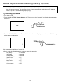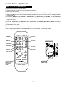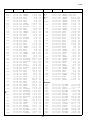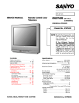
1
FILE NO.
SERVICE MANUAL Colour Television
Model No. CP14SA1(G)
(Australia/New Zealand)
Service Ref. No. CP14SA1-50
(Australia)
CP14SA1-60
(New Zealand)
TV/AV
TIMER
1
2
3
4
5
6
7
8
9
0
-/--
BASS
A B SURROUND
P▲
VIDEO AUDIO
TV/AV MENU
-
+
P
P
CH SCAN
P
P▼
MENU
SWAP
PIC MODE
JXMYA
Specifications
Power Source . . .
Colour System . .
Television System
Channel Coverage
Product Code: 111361917
....
....
....
...
.
.
.
.
. AC220-240V, 50Hz/60Hz.
. PAL (AV input: PAL/NTSC4.43/NTSC/PAL-60Hz)
. B/G
.Australia
VHF: 0-11, 5A
UHF: 28-69
CATV: S1-S41, X, Y, Z, Z+1, Z+2
New Zealand
VHF: 1-11
UHF: 21-69
CATV: S1-S41, X, Y, Z, Z+1, Z+2
Video IF . . . . . . . . . . . . . . 38.0MHz
Aerial Input Impedance . . 75Ω
Ext. Terminals
Video inputs: Phono jack ✕ 2 (1Vp - p, 75Ω)
Audio inputs: Phono jack ✕ 2 (436mVrms, more than 40KΩ)
Video monitor outputs: Phono jack ✕ 1(1Vp - p, 75Ω)
Audio monitor outputs: Phono jack ✕ 1(436mVrms, less than 600Ω)
Sound Output (RMS) . . . . 2 W
Speaker . . . . . . . . . . . . . . Diameter 8cm ✕ 1 pc.
Dimensions . . . . . . . . . . . 364.5 (W) ✕ 361.7 (H) ✕ 375.8 (D)mm
Weight . . . . . . . . . . . . . . . approx. 8.6 Kg
Specifications subject to change without notice.
C5SW/C5SV
Original Version
Chassis Series: AC5-G
- NOTE Service Ref. No. CP14SA1-60 is electrically the
same as Service Ref. No. CP14SA1-50.
The difference between Service Ref. No.
CP14SA1-50 and CP14SA1-60 are as follows:
1) Destination CP14SA1-50...Australia
CP14SA1-60...New Zealand
2 ) The difference in a parts list is only a rated
label.
Give complete “SERVICE REF. NO.” for
parts order or servicing. It is shown on the
rating plate at the cabinet back of the unit.
This T.V. receiver will not work properly in
foreign countries where the television
transmission system and power source differ from the design specifications. Refer to
the specification table.
REFERENCE NO. SM5110466
Contents
Safety Notice . . . . . . . . . . . . . . . . . . . . . . . . . . . . . . . . . . . . . . . . . . . . . . . . . . . . . . . . . . . . . . . . . . . . . . . . 2
Chassis Block Diagram . . . . . . . . . . . . . . . . . . . . . . . . . . . . . . . . . . . . . . . . . . . . . . . . . . . . . . . . . . . . . . 3-4
IC Block Diagrams . . . . . . . . . . . . . . . . . . . . . . . . . . . . . . . . . . . . . . . . . . . . . . . . . . . . . . . . . . . . . . . . . . 5-7
Service Information . . . . . . . . . . . . . . . . . . . . . . . . . . . . . . . . . . . . . . . . . . . . . . . . . . . . . . . . . . . . . . . . . . . 7
Service Adjustments with replacing Memory IC (IC802) . . . . . . . . . . . . . . . . . . . . . . . . . . . . . . . . . . . . . 8-11
Service Mode Adjustments . . . . . . . . . . . . . . . . . . . . . . . . . . . . . . . . . . . . . . . . . . . . . . . . . . . . . . . . . . 12-13
Service Adjustments . . . . . . . . . . . . . . . . . . . . . . . . . . . . . . . . . . . . . . . . . . . . . . . . . . . . . . . . . . . . . . . . . 14
Special Function . . . . . . . . . . . . . . . . . . . . . . . . . . . . . . . . . . . . . . . . . . . . . . . . . . . . . . . . . . . . . . . . . . . . .15
Purity and Convergence Adjustment . . . . . . . . . . . . . . . . . . . . . . . . . . . . . . . . . . . . . . . . . . . . . . . . . . . . . 16
Cabinet Parts List . . . . . . . . . . . . . . . . . . . . . . . . . . . . . . . . . . . . . . . . . . . . . . . . . . . . . . . . . . . . . . . . . . . 17
Chassis Electrical Parts List . . . . . . . . . . . . . . . . . . . . . . . . . . . . . . . . . . . . . . . . . . . . . . . . . . . . . . . . . 18-23
Safety Notice
SAFETY PRECAUTIONS
1: An isolation transformer should be connected in the
power line between the receiver and the AC line
when a service is performed on the primary of the
converter transformer of the set.
3: When replacing a chassis in the cabinet, always be
certain that all the protective devices are installed
properly, such as, control knobs, adjustment covers
or shields, barriers, isolation resistor-capacitor networks etc.. Before returning any television to the
customer, the service technician must be sure that
it is completely safe to operate without danger of
electrical shock.
2: Comply with all caution and safety-related notes provided on the cabinet back, inside the cabinet, on the
chassis or the picture tube.
X-RADIATION PRECAUTION
The primary source of X-RADIATION in television receiver is the picture tube. The picture tube is specially constructed to limit X-RADIATION emissions. For continued X-RADIATION protection, the replacement tube must be
the same type as the original including suffix letter. Excessive high voltage may produce potentially hazardous X
- RADIATION. To avoid such hazards, the high voltage must be maintained within specified limit. Refer to this service manual, high voltage adjustment for specific high voltage limit. If high voltage exceeds specified limits, take
necessary corrective action. Carefully follow the instructions for + B1 volt power supply adjustment, and high voltage check to maintain the high voltage within the specified limits.
PRODUCT SAFETY NOTICE
Product safety should be considered when a component replacement is made in any area of a receiver.
Components indicated by mark
in the parts list and the schematic diagram designate components in which
safety can be of special significance. It is particularly recommended that only parts designated on the parts list
in this manual be used for component replacement designated by mark
. No deviations from resistance
wattage or voltage ratings may be made for replacement items designated by mark
.
-2-
-3-
VIDEO IN
REAR
MONITOR
OUT
REAR
AV IN
IIC Bus
ANT
Key in
28
31
12
1
11
A101
TUNER
VIDEO MONITOR OUT
27
VIF
54
IF
VCC
R
G
B
BLK
AFT
RF AGC
IIC Bus
IF in
AUDIO-OUT
Ext.AUDIO-IN
40
1
51
42
AUDIO-IN
9
5
7
IC001
AUDIO AMP.
(MONO)
3
27 H-OUT
V-OUT
23
ABL
13
AFC
28
MUTE
15V
2
7
6
TELETEXT UNIT
5V-2
Low B
8 9 10 12
IC281
SECAM
SP901
1
SWITCH
13
14 15
9V-1
1
2
Q431
H-DRIVE
T431
H-DRIVE
TRANS.
Reg.
VR631
Q432
H-OUT
Protect
24V
25V
130V
180V
T611
CONVERTER
TRANS.
5
IC501
VERT./DEF.
IIC Bus
16/17
IC2001
TELETEXT DECODER
SECAM KILLER
AUDIO
OUT
B-Y IN
R-Y IN
INT. VIDEO IN
VIDEO-OUT
R
G
B
BLK
R-OUT
19
G-OUT
20
B-OUT
21
34
4
44
46
15
16
17
35
IC201
IF/VIDEO/
CHROMA
8
H-VCC
9V
VIDEO
HOR.
VERT
RGB VCC
VCC
VCC
43
18
25 14
5V-2
9V-1
11/12
6
5
10
SIF
out 52
SIF
in
IF in
10
19
20
21
22
Ext.VIDEO-IN
X161
SAW Filter
IIC Bus
8
Protect
IC801
CPU
1/2
RF AGC
IF OUT
9
6
7
36V
5V-2
4/5
29
3
SDA
Mute
4
Stand by
R/C in
6
AUDIO MONITOR OUT
AUDIO-IN
VIDEO IN
FRONT
AV IN AUDIO-IN
D1910
LED
A1901A
RC
PRE-AMP.
Front
key
SCL
5VRC
AFT
8
TEXT: BLK
5
TEXT: R
TEXT: G
TEXT: B
✻
SELECTED VIDEO OUT
R
B
L902
DY
24V
15V
9V
5VRC
V
H
CRT UNIT
Protect
HV
Q901
CRT
Reg.
Reg.
Reg.
36V
H-VCC
9V-1
5V-2
Protect
POWER SUPPLY CIRCUIT
Low B
Heater
180V
Heater
AFC ABL
T471
FBT
130V
G
9V
✻ Teletext decoder and SECAM
decoder are not equipped.
AUDIO MONITOR OUT
✻
VIDEO IN
IC802
MEMORY
Chassis Block Diagrams
MAIN SIGNAL PROCESSING CIRCUIT
-4-
LED
MUTE OUTPUT
(MUTE ON=HIGH)
32.768KHz
OSC
X801
CPU OSC OUT
CPU OSC IN
ON-TIMER LED OUT (ON TIMER ON=Low)
RC SIGNAL IN
(ACTIVE=HIGH)
RESET INPUT (ACTIVE=LOW)
3
RC PRE-AMP.
IC002
AUDIO AMP.
(MONO)
7
6
32
28
13
29
SCL
IC802
MEMORY
5
3
SDA
6
4
IC801
CPU
QXXABV864
OSD BLK OUT(Active=High)
AFT SIGNAL INPUT
POWER ON/OFF
(ON=HIGH, OFF=LOW)
SDA
SCL
KEY SWITCH IN
17
27
(POWER ERROR=LOW)
POWER PROTECT IN
DEFLECTION
CIRCUIT
POWER CIRCUIT
etc.
VERT. SYNC IN (ACTIVE=LOW)
A101
F/S TUNER
IC201
IF/VIDEO / CHROMA/DEF.
PHOTO COUPLE
KEY
SWITCH
HORIZ. SYNC IN (ACTIVE=LOW)
22
OSD RED OUT(Active=High)
19
OSD GREEN OUT(Active=High)
20
OSD BLUE OUT(Active=High)
21
18
10
31
1
2
12
Chassis Block Diagrams
SYSTEM CONTROL
IC Block Diagrams
IC201 < IF/Video/Chroma/Def. > LA76818A
SIF Output
51
Ext. Audio Input
50
APC Filter
49
VCO Coil 1
48
VCO Coil 2
47
VCO Filter
46
Video Output
45
Black Level Detector
44
Internal Video Input (S-C IN)
A2C
PLL
SIF APC Filter
52
VIDEO
AMP
SIF Input
53
SPLL
TRAP
VIDEO
DET
54
BPF
BPF
LIM
AMP
FM
DET
VIF
IF
IDENT
AFT
CLMP
VIDEO
SW
TRAP
DELAY
LINE
Video/Vertical Vcc
External Video Input(Y-IN)
4.43 MHz Crystal
37
Clamp Filter
36
Chroma APC2 Filter
35
SECAM R-Y Input
(Cr Input)
34
SECAM B-Y Input
(Cb Input)
33
CCD/Horizontal Ground
32
CCD Filter
LPF
ALC
30
31
1H
VCC
1H DELAY
Chroma APC1 Filter
38
CLAMP
DC ADS.
+
Selected Video Output
39
APC2
VCO
SW
Video/Vertical/BUS Ground
40
DDS
TINT
CLAMP
COLOR
CLAMP
VER
SEP
41
VXO
APC1
PAL
SW
DEMO
RGB
MATRIX
CCD Vcc
Clock (4MHz) Outupt
VCO IREF
28
FBP
29
HOR
VCO
1/256
HOR
C/D
AFC1
AFC2
-5-
42
43
V/C VCC
5V
ACC
BPF
ON/OFF
CLMP
SW
SYNC
SEP
CONTRAST
BRIGHT
PHASE
SHIFTER
27
VER
C/D
26
HOR
OUT
25
VER
RAMP
24
FSC/
SYNC SW
23
Horizontal Output
HOR
VCC
H
VCC
22
Horizontal AFC Filter
DC
REST
21
Horizontal/BUS Vcc
OSD
SW
20
Ramp ALC Filter
DRIVE/OUT-OFF
VCC
19
18
Vertical Output
BLACK
STRETCH
17
fsc output or C
Sync output
PEAKING
CORING
16
Fast Blanking Input
OSD
CONTRAST
BRIGHT
15
Blue Input
CLAMP
14
Green Input
Blue Output
IF
AGC
13
Red Input
ABL
12
ABL
BUS
11
Bus Clock
Green Output
SW
10
Bus Data
Red Output
RF
AGC
9
AFT Output
RGB Vcc
DC
VOL
8
FM Filter
IF
VCC 5V
IF Vcc
7
IF Ground
6
PIF Input 2
5
PIF Input1
4
RF AGC Output
3
PIF AGC
2
FM Output/Selected
Audio Output
1
Audio Output
Flyback Pulse Input
SAW
+
9V
PIF
In2
+
IF
GND
IF VCC
RF AGC
Out
IF In
PIF
In1
6
5
4
30K
7
8
120K
12
VIF 2
(6 Vcc)/7
+
-
IF AGC
Def
1bit
0.022u
To
BUS
2ndIF
AGC
VIF 3
to BUS Line
IF AGC
Drive
RF AGC
Delay
6bit
RF
AGC
VIF 1
VIF AMP
BUS
Interface
11
Data Clock
3
PIF
AGC
IF
AGC
APC
Det
Snd
Det
+π/4
-π/4
Video
Det
Sound
Trap
+
50
To
BUS
APC
Filter
VCO.Coil
49
To
BUS
53
Chroma
Counter
FM
Det
Reset
Pulse
A.MUTE
1bit
A.SW
1bit
VIF.Sys
2bit
VCO
Ident
Chroma
C/D
-
+
Input
Select
1000p
FM.Level
5bit
LIM
AMP
0.01u
VIF
Counter
Chroma
VCO
APC
Det
SIF
VCO
500K
BPF
IF
Ident
VCO
COIL2
OSC
C/D
prescaller
500K
Det
VIF
VCO
B/N
INV
48
VCO
COIL1
PLL Pull-in SW
Lock
Det
Video.Level
3bit
Amp
SIF. Sys
2bit
Sound
BPF
SIF.In
54
Amp
330
0.47u
Buzz
Canceller
Amp
SIF.Out
52
10p
Phase
Detector
VOLUME
D/A
VOLUME
Filter
VOLUME
(ATT)
2.5V
+
-
Amp
FM Gain
1bit
AFT
VCO
Alignment
VOLUME
7bit
A.Fil.Def
1bit
FM Mute
1 bit
Deemph
Deem-TC
1bit
FM
Out
+
FM
Filter
47
10
AFT
VCO
Filter
Vcc
+
1 Audio.out
10u
+
Audio in
Video
Out
51
46
9
2
1u
1K
0.01u
0.47u
100K
100K
-6-
0.1u
SIF
APC
Filter
IC Block Diagrams
IC201 <IF System Block Diagram> LA76818A
IC Block Diagrams
IC501 < Vertical Output > LA78040/LA78040N
Thermal
Protection
AMP
+
5
Ver. OUTPUT
GND
PUMP UP
OUT
4
6
7
NON INV.
INPUT
3
2
Vcc
INVERTING
INPUT
1
OUTPUT
STAGE Vcc
Pump
Up
IC001 < Audio AMP.> LA4266
300Ω
30kΩ
1
2
3
4
5
6
NC
NC
Filter
PRE
GND
IN2
NF2
8
7
OUT2 Power
GND
9
10
VCC
NC
Service Information
■ Protection Circuit
This TV set has a built-in power supply protection circuit.
It is provided to protect the TV set in case of a power supply circuit malfunctions. When something abnormality
occurs during TV reception, the TV set goes to the stand-by mode.
When an abnormality occurs during TV reception, it causes pin 27 of the CPU to go continually Low(less than
0.75V) for about one second. The CPU detects that this has occurred and outputs the signal from pin 31 to
switch off the power supply lines.
Releasing the protective circuit and restoring power supply
To release the protective circuit and restore power supply, turn the power to the TV set OFF and then ON again
via either the main power switch or the ON-OFF button on the remote control. This will work only if the power
supply trouble was temporary. If there is permanent trouble such as a damaged circuit, power cannot be
restored and the circuit will have to be repaired.
-7-
Service Adjustments with Replacing Memory IC(IC802)
Note: The CPU (IC801) and memory IC (IC802) store the service adjustments data and controls data for each
circuit.When the Memory IC(IC802) is replaced, some of the service adjustments should be readjusted to
obtain the best performance. The necessary service adjustments are carried out by using the RC handset.
Please set up the TV set with following steps [1] to [2].
[1] Initializing Procedure
1. Put a new memory IC.
2. Turn on the TV set.
3. Press and hold the TV/AV Selector button on the TV set for more than 2 seconds. The following picture appears on
the screen.
TV/AV MENU
CLR
-
+
P
TV/AV Selector
4. Press the PROGRAMME UP on the TV set while the above On-Screen Display is still on the screen. The following
picture appears on the screen.
TV/AV MENU
1
-
+
P
PROGRAMME UP
This completes the initialization of memory IC.
Following shows the initialized contents of memory data by this procedure.
- Plug & Play
: No executed
- Inhibit Data
: Cancelled
- Ch Skip Data
: Cancelled
- Sound Volume Data
: 10/63 steps.
- Volume Lock
: OFF
- Tuning Lock
: OFF
- Music Mode
: OFF
- AV Start
: OFF
- Colour System
: AUTO
-8-
Service Adjustments with Replacing Memory IC(IC802)
[2] Required Service Adjustments
Readjust the following service adjustments.
Adjustments
Service Mode No. & Item
RF AGC
Item 01, RF AGC
Horizontal centre
Item 02, H-PHA
Vertical size
Item 04, V-SIZ
Vertical-S correction
Item 05, V-SCO
Vertical linearity
Item 06, V-LIN
Gray scale
Item 14-17, 19-21
Further adjustment please refer to page 12 and 13.
Following table shows the initial values which have been stored in the CPU ROM, and items for the service adjustments.
Service mode adjustments table in CPU ROM
NO.
ITEM
01
02
03
04
05
06
07
08
09
10
11
12
13
14
15
16
17
18
19
20
21
22
23
24
25
26
27
28
29
RF AGC
H-PHA
V-POS
V-SIZ
V-SCO
V-LIN
H-P60
V-S60
OSDHP
OSDC
V-SCP
H-SCP
SBIAS
RBIAS
GBIAS
BBIAS
RDRIV
GDRIV
BDRIV
1-LINE APPEAR
DRV
B-YD
R-YD
B-YDN
R-YDN
SBDC
SRDC
30
31
32
33
34
35
36
37
38
39
40
41
42
43
44
G-YA
RBGB
RBAG
G-YAN
RBGBN
RBAGN
COGV
BLKS
BLKG
BRTA
BRST
BRTH
WPL
YGAM
PORW
PORS
RFCO
DATA
RANGE
00~63
00~31
00~63
00~127
00~31
00~31
-80~+70
-32~+31
00~255
00~127
00~07
00~07
00~127
00~255
00~255
00~255
00~127
00~15
00~127
00~15
00~15
-08~+07
-08~+07
-08~+07
-08~+07
0,1
00~15
00~15
0,1
-08~+07
-08~+07
00~03
00~03
00~03
0,1
0,1
00~07
00~03
00~03
0,1
00~03
00~03
INITIAL
DATA
30
9
40
59
7
19
+5
0
29
45
7
7
105
0
0
0
64
8
64
10
10
0
0
-8
-5
0
8
8
0
0
0
0
3
3
0
0
0
2
0
0
2
0
DESCRIPTION
RF AGC Adj.
H-Phase (H-Centering) Adj. (50Hz)
V-Position (V-Centering) Adj. (50Hz) Fixed.
V-Size Adj. (50Hz)
V-S Correction (50Hz)
V-Linearity Adj. (50Hz)
H-Centering Adj. (60Hz)
V-Size Adj. (60Hz)
OSD H-Position Adj.
OSD Contrast Adj.
Correction of the V-size accompanying brightness change.
Correction of the H-size accompanying brightness change.
Sub Bias Adj. (Do not change)
Red Bias Adj.
Green Bias Adj.
Blue Bias Adj.
Red Drive Adj.
Green Drive Adj.
Blue Drive Adj.
White Balance Adj.
B-Y DC level Adj.. Colour compensation (PAL)
R-Y DC level Adj.. Colour compensation (PAL)
NTSC B-Y DC level Adj. (Difference value over PAL.)
NTSC R-Y DC level Adj. (Difference value over PAL.)
SECAM B-Y DC level Adj. (Difference value over PAL.)
SECAM R-Y DC level Adj. (Difference value over PAL.)
G-Y angle Adj. (The reproducibility of a colour is changed.)
R-Y, B-Y Gain Blance Adj. (Do not change.)
R-Y, B-Y Angle Adj. (Do not change.)
NTSC G-Y Angle Adj. (Difference value over PAL.)
NTSC R-Y, B-Y Gain Balance Adj. (Difference value over PAL.)
NTSC G-Y, B-Y Angle Adj. (Difference value over PAL)
Coring Adj.
Setting of Black stretch start.
Setting of Black stretch gain.
On and off of ABL.
Setting of ABL.
Setting of ABL.
White peak limitter.
Y Gamma setting.
Switching of Pre-shoot and Over shoot in AV mode.
Pre-shoot/Over shoot Adj. in AV mode.
RF Coring Gain Adj.
-9-
Service Adjustments with Replacing Memory IC(IC802)
NO.
ITEM
DATA
RANGE
45
46
47
48
49
50
51
52
53
54
55
56
57
58
59
60
61
62
63
64
65
66
67
68
PORWN
PORSN
TINT
TINT 443
SHRF
TEXTC
VOLUM
DEEM
VIFSW
SIFSW
V-LVL
FMLVL
IF-TE
IF-T1
IF-T2
IF-T3
H-FRQ
FBTS
COOP
HBLKL
HBLKR
AFCRF
0,1
00~03
-16~+15
-16~+15
-32~+31
-128~+127
00~255
0,1
00~03
00~03
00~07
00~31
0,1
0,1
0,1
00~255
69
70
71
72
73
74
75
76
77
78
79
80
81
82
83
84
VSURF
CDMRF
AFCAV
VSUAV
CDMAV
HLVDRF
HLVDAV
VCO-SW
VCO-ADJ
CROSS-BW
AVNCON
AVNBRI
POMT
CHMT
SYST
S-STE
VOLTBL
CHIP818
INITIAL
DATA
0
0
00~127
00~127
00~255
00~255
00~15
0,1
00~03
0,1
0
-12
0
0
127
0
0
1
4
16
0
1
1
136
34
0
7
7
3
0
0
0
1
0
0
1
1
0
3
0
64
64
25
10
5
0
0
0
00~255
00~255
00~255
00~255
00~255
00~255
00~255
00~255
112
64
0
0
1
0
0
0
00~63
0,1
00~07
00~07
00~07
0,1
0,1
00~07
0,1
0,1
00~07
0,1
0,1
0,1
00~03
00~03
DESCRIPTION
Switching of RF Pre-shoot and Over shoot.
RF Pre-shoot/Over shoot Adj.
RF Tint Adj.
NTSC 4.43 Tint Adj.
RF Sharpness Adj.
OSD TEXT Contrast.
Volume Control Adj.
De emphasis TC.
VIF System Switch.
SIF System Switch.
Video Level Adj.
FM Level Adj.
IF Test.
IF Test-1.
IF Test-2
IF Test-3
Correction of Horizontal Frequency.
Switching of H-blanking and Flyback Pulse.
Setting of Colour Killer Level.
H-Blanking Control. (Left)
H-Blanking Control. (Right)
RF AFC Gain & Gate Adj.
RF V-Sync. Separation Adj.
RF V-Countdown Circuit Adj.
AV AFC Gain & Gate Adj.
AV V-Sync. Separation Adj.
AV V-Countdown Circuit Adj.
Incorrect operation prevention at the time of a special signal (RF mode)
Incorrecr operation prevention at the time of a special signal (AV mode)
C-VCO Adj. Switch.
C-VCO Adj.
Pattern Output.
Contrast Adj. of the blue back in AV mode.
Brightness Adj. of the blue back in AV mode.
Power Mute Time Adj.
Channel Change Mute time Agj.
Selection of the number of times of a Colour system judgment.
Stereo/Mono Option. STEREO=1, MONO=0
Selection of the change characteristic of volume.
Option of 818(1:TINT Control reversal)/828(2:TINT through control) selection.
300
301
302
303
304
305
306
307
308
309
310
311
R09
R10
R11
00~255
00~255
00~255
00~255
33
112
68
0
CPU Debug Date.
CPU Debug Date.
CPU Debug Date.
CPU Debug Date.
CPU Debug Date.
CPU Debug Date.
CPU Debug Date.
CPU Debug Date.
CPU Debug Date.
CPU Debug Date.
CPU Debug Date.
CPU Debug Date.
371
372
R71
R72
00~255
00~255
0
177
CPU Debug Date.
CPU Debug Date.
R00
R01
R02
R03
R04
R05
R06
R07
R08
Notes: The initial value that the CPU writes down the CPU ROM data to the memory when replaced the memory IC.
TV set may not operate correctly with this initial value. It is required to set up the fine adjustment for service
adjustments described in the above.
-10-
Service Adjustments with Replacing Memory IC(IC802)
[Entering to Service Mode]
1. Press and hold the MENU button on the Remote Control and press the VOLUME (+) button on the TV set.
Following setting items appears on the screen.
MENU
Display for [RF AGC] RF AGC adjustment
MENU
Read Status
TV/AV MENU
-
+
SI. 00100101S2.11111000
ADDRESS
DATA
01 RF AGC
30
P
Item No.
Item
Data value
2. Select item by pressing the TIMER (Item No. UP) or SOUND MUTE (Item No. DOWN) button on the remote control
handset.
TIMER
...84➔83➔82➔81➔80......01
01➔02➔03➔04➔05......84...
Example
Display for [V-SCO] V-S Correction adjustment
Display for [DRV] White balance adjustment
Read Status
Read Status
SI. 00100101S2.11111000
ADDRESS
DATA
05 V-SCO
9
Item No.
Item
Data value
SI. 00100101S2.11111000
ADDRESS
DATA
21 DRV R 64
B 64
Item No.
Item
Data value for Blue
Data value for Red
3. Adjust data value by pressing the VOLUME + or VOLUME - button on the remote control handset.
P▲
P▼
To return to normal TV mode, press the MENU button on the TV set or the remote control handset.
-11-
Service Mode Adjustments
Following adjustments should be carried out when the memory IC is replaced. How to enter the service mode and
adjust values, please refer to “ Entering to Service mode” on page 11.
Item 05 [V-SCO] V-S CORRECTION
Item 01 [RF AGC] AGC
NOTE: Do not attempt this adjustment with weak signal.
(1) Tune the receiver to most clearest (or strongest) VHF
station in your area. Set the brightness and contrast
controls to maximum. Set the colour control to
minimum.
(2) Select [RF AGC] in the service mode.
(3) Change value until the snow noise just disappears.
(4) Exit from service mode.
Item 02 [H-PHA] HORIZONTAL CENTRE
(1) Receive a crosshatch pattern.
(2) Set the lever of SW501 (Vertical Center SW) as the
position of a center.
(3) Select a picture mode of NATURAL by pressing the
PICTURE MODE button.
(4) Select [V-SCO] in the service mode.
(5) Adjust Vertical S-letter Correction so that the difference
of “c”, “d” and “e” becomes less than 2 mm by pressing
the VOLUME + or - button.
(6) Confirm Vertical Linearity and adjust Vertical Center
then Vertical Size.
(7) Exit from service mode.
(1) Receive a monochrome circular pattern.
(2) Set the brightness and contrast to normal.
(3) Select [H-PHA] in the service mode.
(4) Change value to be optimum horizontal centre position.
(5) Exit from service mode.
c
Upper
d
Center
e
Bottom
Horizontal centre
Item 06 [V-LIN] VERTICAL LINEARITY
Item 04 [V-SIZ] VERTICAL SIZE
(1) Receive a monochrome circular pattern.
(2) Set the brightness and contrast to maximum.
(3) Select [V-SIZ] in the service mode.
(4) Change value to be optimum vertical size.
(5) Exit from service mode.
(1) Receive a crosshatch pattern.
(2) Set the lever of SW501 (Vertical Center SW) as the
position of a center.
(3) Select a picture mode of NATURAL by pressing the
PICTURE MODE button.
(4) Select [V-LIN] in the service mode.
(5) Adjust Vertical Linearity so that the difference of “a” and
“b” becomes less than 3mm by pressing VOLUME + or
- button.
(6) Exit from service mode.
Upper
Vertical size
a
Center
b
Bottom
-12-
Service Mode Adjustments
Items 14-17, 19-21 GREY SCALE
(1) Receive the monochrome circular pattern.
(2) Set the brightness and colour to normal, contrast to maximum.
(3) Enter to the service mode.
(4) Set each value of Item-14 RBIAS, 15 GBIAS, 16 BBIAS, 17 RDRIV and 19 BDRIV mode to 64.
(5) Select Item-20 mode to be one horizontal scanning line and turn the screen volume on the FBT to obtain just visible
one coloured line.
(6) Press the 1 (Red Bias -), 2 (Red Bias +), 5 (Green Bias -), 6 (Green Bias +), 9 (Blue Bias -) or 0 (Blue Bias +)
button to adjust the brightness of each colour until a dim white line produced. Please see the control button allocations in this mode.
(7) Select Item-21 DRV mode to enter the white balance adjusting mode.
(8) Press the 3 (Red Drive -), 4 (Red Drive +), -/-- (Blue Drive -) or RECALL (Blue Drive +) button alternately to
produce normal black and white picture.
(9) Exit from the service mode.
(10) Check for proper grey scale tracking at all brightness levels.
NOTE: If the grey scale adjustment is made after picture tube replacement, check the high voltage.
Red Drive -
Red Bias +
Red Bias -
TV/AV
TIMER
1
2
3
4
5
6
7
8
Red Drive +
0
KDY-3
-/--
R477
L441
JP646
JP645
Blue Drive +
C437
T471-H2
T471-H12
T471-H10
T471-H7
Blue Bias +
C435-H1
T471
FBT
P
CH SCAN
SCREEN VR
(Under side)
JXMYA
-13-
D485
PIC MODE
R485
R486
Press the MENU
button to exit
from service
mode.
SWAP
R48
R424
MENU
R488
C471
T471-H11
P▼
C435-H4
T471
P
T471-H1
T471-H4
Blue Drive -
C435-H2
A B SURROUND
Blue Bias P▲
L441A
KDY-1
T471A
BASS
L441
KDY-4
L441-H3
9
L631
D432
R355
Green Bias +
6
Green Bias -
MAIN BOARD
1
Service Adjustments
Following adjustments are not required to readjust when replacing the memory IC.
B-VOLTAGE SUPPLY CHECKING
HIGH VOLTAGE CHECK
(1) Connect DC meter to TP-B and the ground.
(2) Tune the receiver to an active channel and synchronized picture. Select NATURAL picture mode by pressing the PICTURE MODE button on the remote control.
(3) Adjust B-voltage to be 130 ± 1V DC by using VR631.
MAIN BOARD
5
R664-H2
R664-H1
C685
D605
C605
-H1
-H2
-H3
-H4
-2
A
KG-3
D663
J808
B
J506
R669
R662-H2
C606
J687
R662-H1
VR631
+B ADJ.
F601B
AC250V 4A
R662
J502
R665
R635
J513
E
JP661
J2
C646
Q661
J603
D604
R637
D686
Q661A
C603
D603
C604
F601
R663
D685
C607
KG
D683
J666
D606
J0
TP-EE
R510
R243
D682
R512
C521
D634
10
10
R515
R514
R525
C524
J641
J642
JP631
R628
R613-H2
IC501-H
R516
R433
R431
R355
L441-H2
KDY-4
D441
J032
JP442
L441-H3
KDY-3
J435
R441
R435
C441-H2
C435-H3
C437
C441-H3
L441
JP646
JP645
L441-H1
L441A
KDY-1
R435A-H1
JP4
C44
C44
C43
C435-H2
T471A
T471-H1
C441-H4
R477
T471-H2
C433
E
C515
Q431
J507
D507
L631
R646
KDY-5
D432
C514
KDY-6
C482
TP-B
JP501
TP-B
C641
C629
R629
J643
1AA4B10S0160A
Q613-H3
J509
JW4
D611
R613
J505
C432
R613-H1
JP502
C518
IC501
V-OUT
C644
C634
C520
T611-H10
R612-H2
L604
J
R519
R518
C631
D631
7
R617
D512
J633
T611-H7
7
Q613-H1
Q613
D633
C611A
R612
C608A
L603
T611
CONVERTER
TRANS.
T611A
R611
C611
J607
C608
R619
E
Q614
C633
T611-H4
R609
C
R642
J645
L605
E
IC501-
R872
J504
R686
R604-H2
Q611
J401
C517
J503
D613
R616
D617 R606
C614
T611-H14
R612-H1
JW3
R687
16
T611-H16
R511
C
J688
R643
16
1
R604
T611-H2
JP683
1
Q683 E
Q613-H2
R607
R618
D662
J604
C613
R620
C643
R615
C628
C662
1
R645
4
R638
J605
R605
C612
E
Q612
JP633
R639
D610
3
R604-H1
2
C607-H2
C607-H1
C610
R603
B-Voltage Supply Adjustment
FOCUS ADJUSTMENT
(1) Receive the monochrome circular pattern.
(2) Set the brightness to normal and contrast to maximum.
(3) Adjust the focus control on the F.B.T. for the best focus
on the screen centre.
MAIN BOARD
D448
Q432-H4
C441B
C441A
JP436
R435A-H2
J033
AUD
TP-A
R426
R424
T471-H11
C471
C407
JP1004
J114
D485
R486
R485
R475
Q432-H5
TP-M
VID
R1001
AUD
D102
K1001
R1007
R422
VID
R105
C101
C106
J1001
AUD
K1002
R1006
C1002
JP1005
C469
Q432-H3
D467
J004
C491
R423
C1001 J1002
R479
D476
C486
R1003
45
R4
R1002
Q432-H1
C436A
Q432-H2
C441
C436
JP437
C441-H1
C435A
C435B
C435-H1
Q432
H-OUT
D421
KQ
C107
C1003
R103
J
D103
JW6
R228
C449
D468
C1004
R501
R435A-H1
R481
1
06
05
178
C132
J105
J106
L432
J438
L431
R435
C441-H2
C435-H4
T471
T471-H12
T471-H10
T471-H7
R488
R441
J435
C435
C435-H2
T471A
T471-H4
T471
FBT
C441-H3
C435-H3
C437
KDY-1
T471-H1
J104
J103
C441-H4
L441
JP646
JP645
L441-H1
X171
T431A
J032
JP442
L441-H3
R477
L441A
T431
H-DRIVE
TRANS.
D441
5
L441-H2
KDY-4
KDY-3
T471-H2
431
1
L631
6
R355
D432
IN
Note: +B (+130V) Voltage Check and Grayscale Adjustment
must be completed before attempting High Voltage Check.
(1) Connect high voltage voltmeter negative lead to
ground, and connect + lead to anode of picture tube.
(2) Tune receiver to an active channel and confirm TV is
operating properly.
(3) Maximize the beam current by adjusting the contrast
and brightness controls to maximum. Confirm high
voltage is within 20.0 KV and 22.0 KV at maximum
beam current.
(4) Eliminate the beam current by adjusting the contrast
and brightness controls to minimum. Confirm high
voltage does not exceed 23.5 KV at zero beam current.
OUT
3
Focus VR
(Upper side)
-14-
If reading is not within range, check horizontal circuit.
No high-voltage adjustment is provided on this chassis.
Special Function
The following special functions can be set up on this TV
set.
How to set the special function:
(1) Volume Lock setting
Note: When making the VOLUME LOCK setting, set the
desired maximum sound volume by pressing the VOLUME + or
- button before entering Special Function setting mode.
With this function, a maximum sound volume limit can be set at
any level.
1
SOUND
18
To enter into the special function setting mode, press and
hold the MENU button of the remote control, then press the
PROGRAMME DOWN button on the TV set.
MENU
VOLUME LOCK
TUNING LOCK
MUSIC MODE
AV START
(2) Tuning Lock setting
Once TUNING LOCK is switched on, further channel tuning
(Pre-set) is not possible. The Channel Swapping function also
is not possible.
NU
-
+
P
SELECT
OFF
OFF
OFF
OFF
ADJUST
M EXIT
TUNING LOCKED
2
(3) Music Mode setting
When Music Mode is ON, Programme position from “91” to “99”
and “0” are set Music Mode. Only sound is provided and any
picture is not on the screen under Music Mode.
P▲
Turns black
screen
MUSIC
Select an item of the special functions by pressing the
PROGRAMME UP or DOWN button on the remote control
or the TV set.
OFF
OFF
OFF
OFF
VOLUME LOCK
TUNING LOCK
MUSIC MODE
AV START
P▼
3
(4) AV Start setting
Set AV-START to ON and every time the TV set is switched on,
AV position will be the initial programme position.
Set the selected special function “ ON “ by pressing the
VOLUME + or - button. To cancel, set to “ OFF”.
P▲
VOLUME LOCK
TUNING LOCK
MUSIC MODE
AV START
OFF
ON
OFF
OFF
AV
P▼
SELECT
ADJUST
M EXIT
4
Press the MENU button of the remote control to return to
the normal TV mode.
MENU
-15-
Purity and Convergence Adjustment
CAUTION: The Convergence and Purity adjustments have been made at the factory. Readjustment
should be made only after picture tube or deflection yoke replacement, following the steps below:
8. Tighten the mounting screw of the Deflection Yoke. Adjust
Convergence next.
PURITY ADJUSTMENT
1. Demagnetize the picture tube and receiver using an external
degaussing coil. When replacing picture tube or deflection
yoke, mount deflection yoke and purity-convergence magnets
assembly properly, see figures 1 and 4.
2. Turn Red and Blue guns off and provide only Green raster.
Rotate Screen control to fully counterclockwise. Rotate Red
and Blue Bias controls fully counterclockwise. Slowly rotate
Green Bias control clockwise to produce Green raster.
3. Loosen the screw holding the Deflection Yoke and remove the
3 Rubber Wedges, and slide the Deflection Yoke fully forward.
4. Rotate and spread the Tabs of the two Purity Magnets to centre the vertical green belt in the picture screen. The Purity
Magnets are also adjusted to obtain vertical centring of the
raster.
5. Slowly slide the Deflection Yoke backward until a uniform
green screen is obtained.
6. Check the purity of the red and blue screens for uniformity,
turn off other colours to check this (use bias controls).
Readjust the yoke position if necessary until all screens are
pure.
7. Adjust each Bias control and screen control to obtain white
raster. Refer to Gray Scale Adjustment. If part of the picture
screen is coloured, adjust the Deflection Yoke position forward
or backward slightly.
CENTRE CONVERGENCE ADJUSTMENT
1. Use a dot crosshatch pattern signal.
2. Turn Red and Blue guns on and turn off Green gun. Adjust the
angle between the Tabs of the Four Pole Magnet 1 and 2, and
superimpose the Red and Blue vertical lines in the centre area
of the picture screen. Refer to figure 2.
3. Keeping the mutual angle of the Tabs of the Four Pole Magnet
turn them together to superimpose the Blue and Red horizontal lines in the centre area of the picture screen. Refer to figure 2.
4. Turn Green gun on and adjust Six Pole Magnet 3 and 4 that
the Green line superimposed on the Red/Blue lines.
This is the same procedure used in steps 2 and 3.
Refer to figure 3.
OUTER AREA CONVERGENCE ADJUSTMENT
Slightly loosen the screw holding the Deflection Yoke. Adjust the
Deflection Yoke to converge the detail in the outer area (left side
and right side) of the picture screen by orbital movement of the
front of the Yoke, then secure the Deflection Yoke in appropriate
position by putting the wedges as illustrated. Tighten screw holding the Deflection Yoke.
DEFLECTION YOKE
PURITY
MAGNET
TABS
SIX-POLE
MAGNET TABS
12
34
FOUR-POLE
MAGNET TABS
ANGLE OF MAGNET TABS
ANGLE
OF TABS
MAGNET TABS
FOCUS GAP
(G3-G4)
RUBBER
WEDGE
DEFLECTION YOKE
MOUNTING SCREW
Figure 1. Purity and Convergence Magnets
Figure 4. Deflection Yoke Movement
Adjust tabs angle to superimpose
blue and red vertical line.
RED
Figure 5. Adjusting Magnet
Adjust tabs together to
superimpose red and
blue horizontal line.
BLUE
Adjust tabs angle to superimpose
red/blue and green vertical line.
GREEN
Adjust tabs together to
superimpose red/blue
and green horizontal
line.
BLUE / RED
Figure- 2 BLUE AND RED LINE MOVEMENT
Figure- 3 BLUE/RED AND GREEN MOVEMENT
-16-
Cabinet Parts List
6
Note: Parts order must contain Service Ref. No., Part No., and descriptions.
4
AUDIO IN
VIDEO IN
ANT. 75Ω
AUDIO OUT VIDEO OUT
5
7
10
8
VIDEO AUDIO
TV/AV MENU
-
+
P
TV/AV
TIMER
1
2
5
9
BASS
3
4
6
7
8
0
-/--
A B SURROUND
P▲
P
P
9
CH SCAN
P▼
3
2
MENU
SWAP
PIC MODE
1
JXMYA
11
Key No.
1
Part No.
300
229
293
299
306
039
Description
2
3
4
5
610
610
610
610
610
645
4686
8406
3741
0430
8800
1866
6
7
610 305 4889
610 305 5251
610 306 1801
8
9
10
or
or
or
or
Key No.
BUTTON POWER-C5SA
SPRING-E3HA
DEC IND-C4SA
BUTTON UNITED-C5TA
CABINET FRONT-C5SW
BADGE,SANYO
CABINET BACK-C5SW
LABEL RATING-C5SW
(CP14SA1-50)
LABEL RATING-C5SV
(CP14SA1-60)
645 054 3579
610 300 5102
ASSY,REMOCON JXMYA
RC-BATTERY LID
610
610
610
645
645
ROD
ROD
ROD
ROD
ROD
011
216
217
012
042
6405
4886
1006
0428
4519
11
or
ANTENNA
ANTENNA
ANTENNA
ANTENNA
ANTENNA
ASSY
ASSY
ASSY
ASSY
ASSY
-17-
Part No.
Description
645 003 2837
610 230 3216
ANT MATCHING BOX
ANT MATCHING BOX
610 305 3547
INSTRUCTIONS MANUAL-C4EY
Chassis Electrical Parts List (Service Ref. No. CP14SA1-50, CP14SA1-60)
C5SW
Product safety should be considered when a component replacement is made in any area of a receiver.
Components indicated by a ! mark in this parts list and the circuit diagram show components whose value have
special significance to product safety. It is particularly recommended that only parts specified on the following parts
list be used for components replacement pointed out by the mark.
Note: Parts order must contain Service Ref. No., Part No., and descriptions. The main PCB unit will be supplied without tuner and
flyback transformer. They should be ordered separately.
Ref. No.
Part No.
Description
Ref. No.
Part No.
Description
OUT OF CIRCUIT BOARD
NOTES:
Read description in the Capacitor and Resistor as follows:
CAPACITOR
CERAMIC 100P K 50V
Rated Voltage
Tolerance Symbols:
Less than 10pF
A : Not specified B : ±0.1pF
D : ±0.5pF
F : ±1PF
R : ±0.25-0pF
S : ±0-0.25pF
More than 10pF
A : Not specified B : ±0.1%
D : ±0.5%
F : ±1%
H : ±3%
J : ±5%
L : ±15%
M : ±20%
P : +100-0%
Q : +30-10%
U : +75-10%
V : +20-10%
X : +40-20%
Y : +150-10%
C : ±0.25pF
G : ±2pF
E : +0-1pF
C : ±0.25%
G : ±2%
K : ±10%
N : ±30%
T : +50-10%
W : +100-10%
Z : +80-20%
PICTURE TUBE
! Q901
414 010 1108
CRT A34KPU02XX
COIL
! L901
! L902
COIL,DEGAUSSING
DEFLECTION YOKE
645 051 5477
645 027 5739
MISCELLANEOUS
SP901
645
652
! W901
645
645
W902
610
028
000
009
048
297
0870
1251
9991
2106
9565
SPEAKER, 8
SPEAKER,8
CORD,POWER
CORD,POWER
ASSY,WIRE GND CONECTOR F8
610 307 2937 ASSY,PWB,MAIN C5SW
1AA0B10S114AA
Rated value: P=pico farad, U=micro farad
Material:
CERAMIC........... Ceramic
MT-PAPER......... Metallized Paper
POLYESTER...... Polyester
MT-POLYEST.....Metallized Polyester
POLYPRO.......... Polypropylene
MT-POLYPRO....Metallized Polypropylene
COMPO FILM.....Composite film
MT-COMPO........Metallized Composite
STYRENE...........Styrene
TA-SOLID........... Tantalum Solid
AL-SOLID........... Aluminium Solid
ELECT................ Electrolytic
NP-ELECT..........Non-polarised Electrolytic
OS-SOLID.......... Aluminium Solid with Organic Semiconductive Electrolytic
DL-ELECT.......... Double Layered Electrolytic
RESISTOR
CARBON 4.7K
J
A
1/4W
Rated Wattage
Performance Symbols:
A: General B: Non flammable Z: Low noise
Other: Temperature coefficient
Tolerance Symbols:
A: ±0.05% B: ±0.1% C: ±0.25% D: ±0.5%
F: ±1%
G: ±2% J: ±5%
K: ±10%
M: ±20% P: +5-15%
Rated value, ohms:
K: 1,000, M: 1,000,000
Material:
CARBON........... Carbon
MT-FILM............ Metal Film
OXIDE-MT......... Oxide Metal Film
SOLID................ Composition
MT-GLAZE......... Metal Glaze
WIRE WOUND... Wire Wound
CERAMIC RES.. Ceramic
FUSIBLE RES.... Fusible
TRANSISTOR
Q111
405 015
Q261
406 000
405 001
405 001
405 004
405 004
405 006
405 006
Q431
405 018
405 018
Q432
406 017
Q611
405 013
405 013
Q612
405 013
405 013
Q613
405 171
Q614
405 006
405 006
Q631
405 014
405 014
405 015
405 015
405 173
405 173
Q661
405 059
405 060
Q681
405 011
405 011
405 011
405 012
405 012
405 012
405 020
405 020
405 020
Q684
405 011
-18-
9701
6804
7407
7605
3109
3208
1707
1806
0507
0606
1809
6801
7006
6801
7006
4107
6504
6702
4509
4608
8704
8902
9803
9902
9903
0005
8401
8500
8609
2002
2101
2309
7501
7709
7907
8401
TR
TR
TR
TR
TR
TR
TR
TR
TR
TR
TR
TR
TR
TR
TR
TR
TR
TR
TR
TR
TR
TR
TR
TR
TR
TR
TR
TR
TR
TR
TR
TR
TR
TR
TR
TR
2SC2814-F4-TB
2SA1015-GR(SAN)
2SA1015-O(SAN)
2SA1015-Y(SAN)
2SA564A-Q(CU)
2SA564A-R(CU)
2SA933S-Q
2SA933S-R
2SC3332-R
2SC3332-S
TT2138LS-YB11
2SC2274-E
2SC2274-F
2SC2274-E
2SC2274-F
2SK2647
2SA984-E
2SA984-F
2SC2412K T146 R
2SC2412K T146 S
2SC2812-L6-TB
2SC2812-L7-TB
2SC3928A1R
2SC3928A1S
2SD1913-R-RA
2SD1913-S-RA
2SC1740S-Q
2SC1740S-R
2SC1740S-S
2SC1815-GR
2SC1815-O
2SC1815-Y
2SC945A-PA
2SC945A-QA
2SC945A-RA
2SC1740S-Q
C5SW
Ref. No.
Q685
Q686
Q818
Q861
Q871
Q881
Q886
Part No.
405
405
405
405
405
405
405
405
405
405
405
405
405
405
405
405
405
405
405
405
405
405
405
405
405
405
405
405
405
405
405
405
405
405
405
405
405
405
405
405
405
405
405
405
405
405
405
405
405
405
405
405
405
405
011
011
012
012
012
020
020
020
014
014
015
015
173
173
134
147
002
002
002
002
173
173
014
014
015
015
173
173
134
147
002
002
002
002
173
173
014
014
015
015
173
173
014
014
015
015
173
173
014
014
015
015
173
173
INTEGRATED CIRCUIT
IC001
409 472
IC201
409 517
IC202
409 241
409 265
409 172
409 320
IC501
409 449
409 507
IC651
409 241
409 265
409 172
Description
8500
8609
2002
2101
2309
7501
7709
7907
4509
4608
8704
8902
9803
9902
5905
2205
0308
0407
6706
6904
9605
9704
4509
4608
8704
8902
9803
9902
5905
2205
0308
0407
6706
6904
9605
9704
4509
4608
8704
8902
9803
9902
4509
4608
8704
8902
9803
9902
4509
4608
8704
8902
9803
9902
TR
TR
TR
TR
TR
TR
TR
TR
TR
TR
TR
TR
TR
TR
TR
TR
TR
TR
TR
TR
TR
TR
TR
TR
TR
TR
TR
TR
TR
TR
TR
TR
TR
TR
TR
TR
TR
TR
TR
TR
TR
TR
TR
TR
TR
TR
TR
TR
TR
TR
TR
TR
TR
TR
2SC1740S-R
2SC1740S-S
2SC1815-GR
2SC1815-O
2SC1815-Y
2SC945A-PA
2SC945A-QA
2SC945A-RA
2SC2412K T146 R
2SC2412K T146 S
2SC2812-L6-TB
2SC2812-L7-TB
2SC3928A1R
2SC3928A1S
2SA1037AK T146 R
2SA1037AK T146 S
2SA1037K-T-96-R
2SA1037K-T-96-S
2SA1179-M6
2SA1179-M7-TB
2SA1235A1E
2SA1235A1F
2SC2412K T146 R
2SC2412K T146 S
2SC2812-L6-TB
2SC2812-L7-TB
2SC3928A1R
2SC3928A1S
2SA1037AK T146 R
2SA1037AK T146 S
2SA1037K-T-96-R
2SA1037K-T-96-S
2SA1179-M6
2SA1179-M7-TB
2SA1235A1E
2SA1235A1F
2SC2412K T146 R
2SC2412K T146 S
2SC2812-L6-TB
2SC2812-L7-TB
2SC3928A1R
2SC3928A1S
2SC2412K T146 R
2SC2412K T146 S
2SC2812-L6-TB
2SC2812-L7-TB
2SC3928A1R
2SC3928A1S
2SC2412K T146 R
2SC2412K T146 S
2SC2812-L6-TB
2SC2812-L7-TB
2SC3928A1R
2SC3928A1S
Ref. No.
IC801
IC802
CAPACITOR
C003
C004
C005
C006
C007
C008
C012
C1001
C1002
C1003
C1004
C101
C106
C107
C111
C112
C113
C120
C121
C122
C123
C132
C135
C138
C171
C172
C174
C178
C1902
C201
C202
C203
C204
4408
5902
5407
4806
1509
5700
4103
0900
5407
4806
1509
IC LA4266
IC LA76818A
IC BA178M05T
IC L78M05CV
IC MC78M05CT
IC UPC78M05AHF
IC LA78040
IC LA78040N
IC BA178M05T
IC L78M05CV
IC MC78M05CT
C205
C208
C209
C210
C211
C212
C221
-19-
Part No.
Description
409 320 5700
410 406 3305
409 383 6805
IC UPC78M05AHF
IC LC863440V-5Y67-TLM
IC 24LC08B/P
404
403
404
403
404
403
404
403
403
403
404
403
403
404
403
404
403
403
403
404
403
404
403
404
403
403
403
403
403
403
404
403
401
404
403
404
403
403
403
403
403
404
403
404
403
404
403
403
403
403
404
403
404
403
403
404
403
404
403
403
403
403
ELECT
ELECT
ELECT
ELECT
ELECT
ELECT
ELECT
ELECT
POLYESTER
POLYESTER
ELECT
ELECT
CERAMIC
ELECT
ELECT
ELECT
ELECT
ELECT
ELECT
ELECT
ELECT
ELECT
ELECT
ELECT
ELECT
CERAMIC
CERAMIC
CERAMIC
MT-COMPO
CERAMIC
ELECT
ELECT
MT-GLAZE
ELECT
ELECT
ELECT
ELECT
CERAMIC
CERAMIC
CERAMIC
CERAMIC
ELECT
ELECT
ELECT
ELECT
NP-ELECT
NP-ELECT
POLYESTER
POLYESTER
CERAMIC
ELECT
ELECT
ELECT
ELECT
CERAMIC
ELECT
ELECT
ELECT
ELECT
CERAMIC
CERAMIC
CERAMIC
089
044
084
051
089
044
087
047
057
181
084
045
215
084
049
084
049
049
043
084
044
084
051
084
051
215
215
215
249
215
084
042
105
084
048
084
048
284
113
367
157
084
049
087
050
084
086
058
179
215
084
049
084
049
367
084
048
084
051
367
155
305
7200
9501
9209
0607
7200
9501
5109
5005
3107
8207
8400
1504
2201
8905
4204
8806
0008
4204
0202
8301
1703
9308
3103
9308
3103
2201
2201
2201
9207
2201
7809
2405
7909
8707
6308
8707
6308
4304
3805
0407
1904
8806
0008
5406
2800
9803
2300
2604
3207
2201
8905
4204
8905
4204
0407
8707
6308
8301
4209
0407
4204
3507
100U M
25V
100U M
25V
4.7U M
50V
4.7U M
50V
100U M
25V
100U M
25V
470U M
25V
470U M
25V
0.1U K
50V
0.1U K
50V
1000U M
25V
1000U M
25V
0.01U K
50V
10U M
50V
10U M
50V
1U M
50V
1U M
50V
10U M
50V
220U M
16V
470U M
16V
470U M
16V
47U M
50V
47U M
50V
47U M
50V
47U M
50V
0.01U K
50V
0.01U K
50V
0.01U K
50V
0.022U J
50V
0.01U K
50V
100U M
16V
100U M
16V
0.000 ZA 1/16W
0.47U M
50V
0.47U M
50V
0.47U M
50V
0.47U M
50V
0.022U K
50V
1000P K
50V
0.1U K
50V
10P D
50V
1U M
50V
1U M
50V
22U M
50V
22U M
50V
1U M
50V
1U M
50V
0.015U J
50V
0.015U J
50V
0.01U K
50V
10U M
50V
10U M
50V
10U M
50V
10U M
50V
0.1U K
50V
0.47U M
50V
0.47U M
50V
470U M
16V
470U M
50V
0.1U K
50V
15P J
50V
0.1U Z
50V
C5SW
Ref. No.
Part No.
C222
C223
C224
C225
403
403
403
404
403
404
403
403
403
403
404
403
403
403
404
403
404
403
404
403
404
403
403
403
404
403
403
403
404
403
404
403
403
404
403
404
404
404
403
404
403
404
403
404
403
404
403
403
404
403
403
403
404
404
404
404
404
404
403
403
403
403
403
403
403
403
403
C226
C230
C231
C232
C233
C234
C243
C244
C245
C246
C247
C273
C283
C358
C432
C433
C434
C435
C441
C469
C471
C482
C510
C514
C515
C517
C518
C521
C524
!
C601
C602
C607
C608
C610
C611
C612
C613
C614
305
305
367
084
049
084
049
215
260
260
084
049
215
215
084
051
084
086
084
049
084
049
164
215
084
049
075
076
087
054
066
349
346
084
049
056
084
084
045
088
042
084
049
084
045
084
053
072
084
054
064
276
093
089
093
089
038
067
247
325
049
247
237
243
178
249
056
Description
3507
3507
0407
8806
0008
8806
0008
2201
2904
2904
8905
4204
2201
2201
9308
3103
9803
2300
8806
0008
9001
9803
0204
2201
8806
0008
7101
3102
6007
0703
5106
3501
7304
8905
4204
5307
9902
8400
1504
7300
7707
8905
4204
8400
1504
9407
2104
9405
9506
1502
1202
9706
6107
1505
6107
1505
1600
4009
1609
5109
0008
5003
8007
6806
9408
8903
9704
CERAMIC
0.1U Z
50V
CERAMIC
0.1U Z
50V
CERAMIC
0.1U K
50V
ELECT
1U M
50V
ELECT
1U M
50V
ELECT
1U M
50V
ELECT
1U M
50V
CERAMIC
0.01U K
50V
MT-COMPO
0.33U J
50V
MT-COMPO
0.33U J
50V
ELECT
10U M
50V
ELECT
10U M
50V
CERAMIC
0.01U K
50V
CERAMIC
0.01U K
50V
ELECT
47U M
50V
ELECT
47U M
50V
NP-ELECT
1U M
50V
NP-ELECT
1U M
50V
ELECT
1U M
50V
ELECT
1U M
50V
ELECT
2.2U M
50V
ELECT
2.2U M
50V
CERAMIC
0.1U Z
25V
CERAMIC
0.01U K
50V
ELECT
1U M
50V
ELECT
1U M
50V
CERAMIC
1000P K 500V
CERAMIC
3900P K 500V
ELECT
47U M
35V
ELECT
47U M
35V
MT-POLYPRO 5400P H 1.5K
MT-POLYPRO 0.36U J 200V
MT-POLYPRO 0.36U J 250V
ELECT
10U M
50V
ELECT
10U M
50V
NP-ELECT
2.2U M 100V
NP-ELECT
2.2U M 100V
ELECT
1000U M
25V
ELECT
1000U M
25V
ELECT
22U M
16V
ELECT
22U M
16V
ELECT
10U M
50V
ELECT
10U M
50V
ELECT
1000U M
25V
ELECT
1000U M
25V
ELECT
220U M
35V
ELECT
220U M
35V
CERAMIC
3300P K
50V
ELECT
470U M
35V
ELECT
470U M
35V
POLYESTER
0.1U K 100V
POLYESTER
0.1U K 100V
MT-POLYEST
0.1U M 275V
MT-POLYEST
0.1U M 275V
MT-POLYEST
0.1U M 275V
MT-POLYEST
0.1U M 275V
ELECT
100U M 400V
ELECT
100U M 400V
CERAMIC
220P K
1K
CERAMIC
220P K
1K
ELECT
1U M
50V
CERAMIC
470P K
1K
MT-COMPO
0.1U J
50V
MT-COMPO
0.1U J
50V
POLYESTER 0.012U J
50V
MT-COMPO
0.012U J 50V
POLYESTER
0.01U J
50V
Ref. No.
Part No.
Description
C894
403
404
404
404
404
404
403
403
403
403
403
403
404
404
403
404
403
403
404
403
404
403
404
403
403
403
403
404
403
403
403
403
403
404
403
403
403
403
404
403
403
403
404
403
403
178
073
073
073
073
088
247
269
247
269
247
269
080
084
054
084
045
039
084
043
084
044
084
049
155
157
215
084
041
342
367
157
342
084
049
157
157
157
084
049
155
342
084
049
281
9309
5106
3300
3904
2105
3104
5003
1809
5003
1809
5003
1809
0606
9506
1502
8400
1504
6508
8004
0202
8301
1703
8806
0008
4204
2505
2201
7700
8804
3300
0407
3601
3300
8806
0008
3106
3106
3106
8806
0008
2200
3300
9001
9803
5007
POLYESTER
0.01U J
CERAMIC 470P K 250V
CERAMIC 470P M 250V
CERAMIC
1000P K
CERAMIC
1000P M
CERAMIC
1000P M
CERAMIC
470P K
CERAMIC
470P K
CERAMIC
470P K
CERAMIC
470P K
CERAMIC
470P K
CERAMIC
470P K
ELECT
100U M
ELECT
470U M
ELECT
470U M
ELECT
1000U M
ELECT
1000U M
ELECT
100U M
ELECT
220U M
ELECT
220U M
ELECT
470U M
ELECT
470U M
ELECT
1U M
ELECT
1U M
CERAMIC
15P J
CERAMIC
27P J
CERAMIC
0.01U K
ELECT
10U M
ELECT
10U M
CERAMIC
0.1U K
CERAMIC
0.1U K
CERAMIC
100P J
CERAMIC
0.1U K
ELECT
1U M
ELECT
1U M
CERAMIC
56P J
CERAMIC
56P J
CERAMIC
56P J
ELECT
1U M
ELECT
1U M
CERAMIC
3300P K
CERAMIC
0.1U K
ELECT
2.2U M
ELECT
2.2U M
CERAMIC
0.033U K
RESISTOR
R003
R004
R005
R006
R010
R011
R1001
R1002
R1003
R1004
R1005
R1006
R1007
R103
R106
R107
R108
R109
R111
R112
401
401
401
401
401
401
401
401
401
401
401
401
401
401
401
401
401
401
401
401
113
105
025
024
105
105
027
105
105
105
105
027
024
061
024
024
105
105
105
105
5607
0702
1308
5604
3307
2904
6608
0504
0702
6506
0702
6608
7707
8101
6700
6700
2102
8203
0504
6001
MT-GLAZE
750 JA 1/16W
MT-GLAZE
100K JA 1/16W
CARBON
150 JA 1/6W
CARBON 1 JA 1/6W
MT-GLAZE
2.7K JA 1/16W
MT-GLAZE
22K JA 1/16W
CARBON
75 JA 1/6W
MT-GLAZE
1K JA 1/16W
MT-GLAZE
100K JA 1/16W
MT-GLAZE
680 JA 1/16W
MT-GLAZE
100K JA 1/16W
CARBON
75 JA 1/6W
CARBON
100K JA 1/6W
OXIDE-MT
39K JA
1W
CARBON
100 JA 1/6W
CARBON
100 JA 1/6W
MT-GLAZE
18K JA 1/16W
MT-GLAZE
68K JA 1/16W
MT-GLAZE
1K JA 1/16W
MT-GLAZE
5.6K JA 1/16W
!
C627
!
C629
C631
C633
C634
C641
C643
C644
C651
C661
C662
C685
C801
C802
C803
C805
C823
C824
C825
C829
C835
C851
C852
C853
C861
C888
C892
C893
-20-
50V
250V
250V
250V
1K
1K
1K
1K
1K
1K
160V
35V
35V
25V
25V
10V
16V
16V
16V
16V
50V
50V
50V
50V
50V
16V
16V
25V
50V
50V
25V
50V
50V
50V
50V
50V
50V
50V
50V
25V
50V
50V
25V
C5SW
Ref. No.
R114
R115
R116
R130
R132
R140
R141
R176
R185
R1902
R1903
R1904
R1905
R1906
R1907
R1911
R1912
R1913
R209
R210
R211
R212
R221
R222
R223
R224
R225
R226
R227
R228
R229
R230
R244
R245
R263
R264
R265
R267
R271
R272
R280
R282
R284
R286
R340
R351
R352
R354
R355
R356
R357
R358
R422
R423
R424
R426
R432
R433
R434
R445
R475
R479
R481
R501
R510
R511
R514
Part No.
401
401
401
401
401
401
401
401
401
401
401
401
401
401
401
401
401
401
401
401
401
401
401
401
401
401
401
401
401
401
401
401
401
401
401
401
401
401
401
401
401
401
401
401
401
401
401
401
401
401
401
401
401
401
401
401
401
401
401
401
401
401
401
401
401
401
401
105
027
105
105
105
105
105
105
068
105
105
105
105
105
024
105
105
105
113
105
025
025
105
105
105
105
105
105
105
024
105
026
105
105
105
026
105
026
105
105
024
105
105
105
105
027
012
025
015
105
026
105
023
023
024
024
024
007
008
068
009
025
068
064
025
024
025
Description
4007
2105
5806
7909
5202
5905
5905
0603
1600
3406
1105
6001
4601
2805
6700
2706
2706
2706
9506
3703
1308
1308
0504
0504
0504
5301
5301
3406
4205
7707
6704
9303
5400
5400
0603
0607
3901
0607
0405
0405
6700
4106
4106
5301
7503
8602
7009
8208
3800
0603
7002
7909
3700
3700
7004
7400
7004
1104
6702
7800
5803
7805
1600
8702
8208
7400
1902
Ref. No.
MT-GLAZE
330 JA 1/16W
CARBON
56 JA 1/6W
MT-GLAZE
56 JA 1/16W
MT-GLAZE
0.000 ZA 1/16W
MT-GLAZE
470 JA 1/16W
MT-GLAZE
560 JA 1/16W
MT-GLAZE
560 JA 1/16W
MT-GLAZE
10K JA 1/16W
OXIDE-MT
4.7 JA
2W
MT-GLAZE
27K JA 1/16W
MT-GLAZE
12K JA 1/16W
MT-GLAZE
5.6K JA 1/16W
MT-GLAZE
3.9K JA 1/16W
MT-GLAZE
2.2K JA 1/16W
CARBON
100 JA 1/6W
MT-GLAZE
220 JA 1/16W
MT-GLAZE
220 JA 1/16W
MT-GLAZE
220 JA 1/16W
MT-GLAZE
620K JA 1/16W
MT-GLAZE
3K JA 1/16W
CARBON
150 JA 1/6W
CARBON
150 JA 1/6W
MT-GLAZE
1K JA 1/16W
MT-GLAZE
1K JA 1/16W
MT-GLAZE
1K JA 1/16W
MT-GLAZE
4.7K JA 1/16W
MT-GLAZE
4.7K JA 1/16W
MT-GLAZE
27K JA 1/16W
MT-GLAZE
33K JA 1/16W
CARBON
100K JA 1/6W
MT-GLAZE
680K JA 1/16W
CARBON
47 JA 1/6W
MT-GLAZE
47K JA 1/16W
MT-GLAZE
47K JA 1/16W
MT-GLAZE
10K JA 1/16W
CARBON
270 JA 1/6W
MT-GLAZE
33 JA 1/16W
CARBON
270 JA 1/6W
MT-GLAZE
100 JA 1/16W
MT-GLAZE
100 JA 1/16W
CARBON
100 JA 1/6W
MT-GLAZE
3.3K JA 1/16W
MT-GLAZE
3.3K JA 1/16W
MT-GLAZE
4.7K JA 1/16W
MT-GLAZE
82K JA 1/16W
CARBON
8.2K JA 1/6W
CARBON
10K JA 1/4W
CARBON
22K JA 1/6W
CARBON
18K JA 1/4W
MT-GLAZE
10K JA 1/16W
CARBON
3.9K JA 1/6W
MT-GLAZE
0.000 ZA 1/16W
CARBON 82K JA 1/4W
CARBON 82K JA 1/4W
CARBON
1K JA 1/6W
CARBON
10K JA 1/6W
CARBON
1K JA 1/6W
CARBON
1K JA 1/2W
CARBON
220 JA 1/2W
OXIDE-MT
560 JA
2W
CARBON
330 JA 1/2W
CARBON
2.2K JA 1/6W
OXIDE-MT
4.7 JA
2W
OXIDE-MT
1K JA
2W
CARBON
22K JA 1/6W
CARBON
10K JA 1/6W
CARBON
15K JA 1/6W
R515
R516
R518
R522
R525
R602
R603
R604
R605
R606
R607
R609
R611
R612
R613
R615
R616
R617
R618
R619
R620
! R628
! R629
R635
R636
R637
R638
R639
R642
R643
R644
R645
R646
R661
R662
R663
R664
R681
R682
R683
R684
R685
R688
R689
R801
R804
R805
R811
R812
R813
R814
R815
R816
R817
R818
R819
R821
R822
R830
R831
R833
R834
R835
R836
R837
R838
R839
-21-
Part No.
401
401
401
401
401
402
401
401
401
401
401
401
401
402
401
401
401
402
401
401
401
402
402
401
401
401
401
401
401
402
401
401
401
401
401
401
401
401
401
401
401
401
401
401
401
401
401
401
401
401
401
401
401
401
401
401
401
401
401
401
401
401
401
401
401
401
401
026
027
009
024
008
060
010
066
010
027
019
025
025
001
064
016
027
092
024
025
020
000
000
007
105
007
061
013
012
001
142
026
026
060
065
013
065
024
026
105
105
105
025
027
105
105
105
105
105
105
105
105
105
105
024
105
105
105
105
105
105
105
105
105
105
105
105
1307
2600
3106
9008
6702
8109
9203
9103
9203
0507
9600
8208
8208
8502
3806
1508
2600
1307
7004
8208
0801
8305
8305
2309
5301
9308
4400
6407
7009
8700
9508
3905
1307
7402
1801
6407
1801
7004
9907
6100
0603
2904
8208
3201
3505
7909
7909
3406
0603
0603
0603
0603
0603
3307
7004
0603
0603
7909
0504
5202
0603
0603
0603
0603
1600
1600
4007
Description
CARBON
27K
CARBON
5.6K
CARBON
3.3
CARBON
120
CARBON
220
WIRE WOUND
3.9
CARBON
560K
OXIDE-MT
27
CARBON
560K
CARBON
470K
CARBON
47
CARBON
22K
CARBON
22K
FUSIBLE RES
10
OXIDE-MT
1.0
CARBON
22
CARBON
5.6K
FUSIBLE RES 680
CARBON
1K
CARBON
22K
CARBON
470
SOLID
5.6M
SOLID
5.6M
CARBON
100K
MT-GLAZE
4.7K
CARBON
150K
OXIDE-MT
33K
CARBON
12K
CARBON
10K
FUSIBLE RES
18
OXIDE-MT
0.27
CARBON
330
CARBON
27K
OXIDE-MT
270
OXIDE-MT
12
CARBON
12K
OXIDE-MT
12
CARBON
1K
CARBON
4.7K
MT-GLAZE
560K
MT-GLAZE
10K
MT-GLAZE
22K
CARBON
22K
CARBON
560K
MT-GLAZE
270K
MT-GLAZE
0.000
MT-GLAZE
0.000
MT-GLAZE
27K
MT-GLAZE
10K
MT-GLAZE
10K
MT-GLAZE
10K
MT-GLAZE
10K
MT-GLAZE
10K
MT-GLAZE
2.7K
CARBON
1K
MT-GLAZE
10K
MT-GLAZE
10K
MT-GLAZE
0.000
MT-GLAZE
1K
MT-GLAZE
470
MT-GLAZE
10K
MT-GLAZE
10K
MT-GLAZE
10K
MT-GLAZE
10K
MT-GLAZE
15K
MT-GLAZE
15K
MT-GLAZE
330
JA
JA
JA
JA
JA
KA
JA
JA
JA
JA
JA
JA
JA
JJA
JA
JA
JJA
JA
JA
KA
KA
JA
JA
JA
JA
JA
JA
JJA
JA
JA
JA
JA
JA
JA
JA
JA
JA
JA
JA
JA
JA
JA
ZA
ZA
JA
JA
JA
JA
JA
JA
JA
JA
JA
JA
ZA
JA
JA
JA
JA
JA
JA
JA
JA
JA
1/6W
1/6W
1/2W
1/6W
1/2W
5W
1/2W
2W
1/2W
1/6W
1/4W
1/6W
1/6W
1/2W
2W
1/4W
1/6W
1/2W
1/6W
1/6W
1/4W
1/2W
1/2W
1/2W
1/16W
1/2W
1W
1/4W
1/4W
1/2W
1W
1/6W
1/6W
1W
2W
1/4W
2W
1/6W
1/6W
1/16W
1/16W
1/16W
1/6W
1/6W
1/16W
1/16W
1/16W
1/16W
1/16W
1/16W
1/16W
1/16W
1/16W
1/16W
1/6W
1/16W
1/16W
1/16W
1/16W
1/16W
1/16W
1/16W
1/16W
1/16W
1/16W
1/16W
1/16W
C5SW
Ref. No.
Part No.
R840
R841
R842
R845
R851
R853
R855
R857
R861
R862
R863
R866
R869
R870
R871
R872
R873
R874
R875
R876
R877
R881
R882
R883
R886
R892
R893
R894
401
401
401
401
401
401
401
401
401
401
401
401
401
401
401
401
401
401
401
401
403
401
401
401
401
401
401
401
105
105
105
105
025
027
027
027
105
105
105
024
024
105
105
026
105
105
105
105
157
105
105
105
105
105
105
105
Description
4007
5301
5301
5400
1605
8602
8602
8602
1501
7404
5400
6700
6700
2904
0603
1307
4205
0603
0603
5400
7203
4106
4106
4205
2904
5509
8005
0405
MT-GLAZE
MT-GLAZE
MT-GLAZE
MT-GLAZE
CARBON
CARBON
CARBON
CARBON
MT-GLAZE
MT-GLAZE
MT-GLAZE
CARBON
CARBON
MT-GLAZE
MT-GLAZE
CARBON
MT-GLAZE
MT-GLAZE
MT-GLAZE
MT-GLAZE
CERAMIC
MT-GLAZE
MT-GLAZE
MT-GLAZE
MT-GLAZE
MT-GLAZE
MT-GLAZE
MT-GLAZE
Ref. No.
330 JA
4.7K JA
4.7K JA
47K JA
1.5K JA
8.2K JA
8.2K JA
8.2K JA
1.5K JA
8.2K JA
47K JA
100 JA
100 JA
22K JA
10K JA
27K JA
33K JA
10K JA
10K JA
47K JA
3900P K
3.3K JA
3.3K JA
33K JA
22K JA
470K JA
1M JA
100 JA
VARIABLE RESISTOR
VR631
645 006 5125
652 000 0100
VR, SEMI, 2K N
VR,SEMI,2K N
TRANSFORMER
T431
652 001 1144
! T471
645 056 7209
! T611
645 058 8051
TRANS,DRIVE
TRANS, FLYBACK
TRANS,POWER,PULSE
COIL
L171
L234
L235
L236
L431
L432
!
L601
L603
L604
L605
L631
DIODE
D005
D102
D103
645
645
401
401
401
610
610
645
610
645
652
610
610
645
645
652
645
652
645
645
652
049
054
024
024
024
032
032
008
031
018
001
031
031
018
018
001
018
001
005
018
001
3379
0271
9008
9008
9008
4381
4404
5642
9998
7025
0475
5945
5969
9265
9722
0147
9722
0147
0763
9722
0147
TRANS,OSC,38MHZ
TRANS,OSC,38MHZ
CARBON
120 JA
CARBON
120 JA
CARBON
120 JA
FILTER COIL
FILTER COIL
INDUCTOR,3.3U K
PIPE CORE
CORE,PIPE
PIPE CORE
LINE FILTER
LINE FILTER
LINE FILTER
CORE,PIPE
CORE,PIPE
CORE,PIPE
CORE,PIPE
CORE,PIPE
CORE,PIPE
CORE,PIPE
407
407
407
408
407
149
099
057
047
100
0807
5600
4003
8605
0204
DIODE
ZENER
ZENER
ZENER
ZENER
1/16W
1/16W
1/16W
1/16W
1/6W
1/6W
1/6W
1/6W
1/16W
1/16W
1/16W
1/6W
1/6W
1/16W
1/16W
1/6W
1/16W
1/16W
1/16W
1/16W
50V
1/16W
1/16W
1/16W
1/16W
1/16W
1/16W
1/16W
D122
D1910
D1910A
D352
D357
D421
D432
D467
D468
D476
D512
D603
D604
D605
D606
! D610
D611
D613
D617
D631
D633
1/6W
1/6W
1/6W
D634
D661
D681
D683
D685
D686
D861
1SS355-TE-17
DIODE MTZJ6.8A
DIODE RD6.8EB1
DIODE MTZJ6.8A
DIODE MTZJ36A
Part No.
407
408
401
407
610
610
407
407
408
407
408
407
407
407
407
407
407
408
407
408
407
407
407
407
407
408
407
407
407
407
407
407
407
407
407
407
408
407
407
407
407
407
407
407
408
407
408
407
407
407
407
408
407
407
407
407
407
408
407
407
408
407
408
056
047
105
116
264
273
063
056
047
005
008
012
013
013
099
054
054
047
009
008
013
013
012
099
057
047
005
006
006
006
006
230
231
012
099
057
047
006
009
007
007
009
099
054
047
005
008
012
013
013
005
008
012
013
013
099
057
047
099
057
047
055
041
Description
2307
6205
7909
6504
5064
7929
8705
9801
7103
4505
2406
4406
4306
7109
7208
7007
7205
5307
8905
2406
4306
6508
4406
5600
4003
8605
8602
6300
6300
6300
6300
3908
7707
4406
5907
8407
9800
0100
8905
7603
7801
8905
6102
0008
2306
4505
2406
4406
4306
7109
4505
2406
4406
4306
7109
5600
4003
8605
5501
2801
8308
7907
2005
MISCELLANEOUS
! F601
423 028 8603
423 024 8409
-22-
ZENER DIODE RD36EB1
ZENER DIODE MTZJ36A
MT-GLAZE
0.000 ZA 1/16W
LED SLP-181B-51
HOLDER LED-S2CP
HOLDER LED-S4KF
ZENER DIODE MTZJ5.1C
ZENER DIODE RD5.6EB1
ZENER DIODE MTZJ5.1C-52
DIODE DS442X
DIODE 1N4148
DIODE 1SS133
DIODE 1S2076A
DIODE 1S2473
ZENER DIODE MTZJ16A
ZENER DIODE RD16EB1
ZENER DIODE RD16EB3
ZENER DIODE MTZJ16A-52
DIODE RU3M
DIODE 1N4148
DIODE 1S2076A
DIODE 1S2471
DIODE 1SS133
ZENER DIODE MTZJ6.8A
ZENER DIODE RD6.8EB1
ZENER DIODE MTZJ6.8A
DIODE ERA15-02
DIODE ERC05-10B
DIODE ERC05-10B
DIODE ERC05-10B
DIODE ERC05-10B
PHOTO COUPLE PC123Y52
PC TLP421F(D4-BL)
DIODE 1SS133
ZENER DIODE MTZJ8.2C
ZENER DIODE RD8.2EB3
ZENER DIODE MTZJ8.2C
DIODE ERA91-02
DIODE RU3M
DIODE EU2
DIODE EU2Z
DIODE RU3M
ZENER DIODE MTZJ10B
ZENER DIODE RD10EB2
ZENER DIODE MTZJ10B
DIODE DS442X
DIODE 1N4148
DIODE 1SS133
DIODE 1S2076A
DIODE 1S2473
DIODE DS442X
DIODE 1N4148
DIODE 1SS133
DIODE 1S2076A
DIODE 1S2473
ZENER DIODE MTZJ6.8A
ZENER DIODE RD6.8EB1
ZENER DIODE MTZJ6.8A
ZENER DIODE MTZJ6.2C
ZENER DIODE RD6.2EB3
ZENER DIODE MTZJ6.2C-52
ZENER DIODE RD3.6EL
ZENER DIODE RD3.6EL
FUSE
FUSE
250V
250V
4A
4A
C5SW
Ref. No.
F601A
F601B
A101
A1901A
K1002
!
K1003
PS601
SW1901
SW1902
SW1903
SW1904
SW1905
SW1906
!
SW601
X161
X211
X801
Part No.
645
645
645
645
645
645
645
645
408
645
645
645
645
645
645
645
645
645
645
645
645
645
645
645
645
645
645
645
421
645
652
645
645
040
040
051
057
047
011
002
040
046
003
019
027
003
019
027
003
019
027
003
019
027
003
019
027
003
019
027
059
009
024
001
004
004
Description
3576
3576
8423
2753
6228
2973
1800
1275
4400
4701
4887
7382
4701
4887
7382
4701
4887
7382
4701
4887
7382
4701
4887
7382
4701
4887
7382
0061
4606
8818
0154
1938
1945
Ref. No.
HOLDER,FUSE
HOLDER,FUSE
TUNER,U/V
TUNER,U/V
UNIT,REMOCON RECEIVER
JACK,RCA-2
TERMINAL,BOARD
JACK,RCA-2
THERMISTOR PTDAA1BF9R0Q20
SWITCH,PUSH 1P-1TX1
SWITCH,PUSH 1P-1TX1
SWITCH,PUSH 1P-1TX1
SWITCH,PUSH 1P-1TX1
SWITCH,PUSH 1P-1TX1
SWITCH,PUSH 1P-1TX1
SWITCH,PUSH 1P-1TX1
SWITCH,PUSH 1P-1TX1
SWITCH,PUSH 1P-1TX1
SWITCH,PUSH 1P-1TX1
SWITCH,PUSH 1P-1TX1
SWITCH,PUSH 1P-1TX1
SWITCH,PUSH 1P-1TX1
SWITCH,PUSH 1P-1TX1
SWITCH,PUSH 1P-1TX1
SWITCH,PUSH 1P-1TX1
SWITCH,PUSH 1P-1TX1
SWITCH,PUSH 1P-1TX1
SWITCH, POWER 1P-1TX1
SAW F TSF5419P
OSC,CRYSTAL 4.433619MHZ
OSC,CRYSTAL 4.433619MHZ
OSC,CRYSTAL 32.768KHZ
OSC,CRYSTAL 32.768KHZ
610 307 2951 ASSY,PWB,CRT C4EY
1AA0B10S1140B
TRANSISTOR
Q701
406
406
405
405
Q703
406
406
405
405
Q705
406
406
405
405
Q721
405
405
Q751
405
405
405
405
405
405
CAPACITOR
C708
C710
C751
404
403
403
403
403
404
000
000
040
029
000
000
040
029
000
000
040
029
001
001
002
002
002
002
173
173
5104
5203
5600
6901
5104
5203
5600
6901
5104
5203
5600
6901
7407
7605
0308
0407
6706
6904
9605
9704
TR
TR
TR
TR
TR
TR
TR
TR
TR
TR
TR
TR
TR
TR
TR
TR
TR
TR
TR
TR
084
077
077
312
368
084
6505
2708
2807
8304
8907
7809
CERAMIC
CERAMIC
CERAMIC
CERAMIC
ELECT
ELECT
K
P
Z
Z
M
M
Description
403 042 2405
ELECT
RESISTOR
R701
R702
R704
R705
R707
R708
R711
R712
R713
R715
R718
R719
R723
R724
R743
R751
R752
R753
401
401
401
401
401
401
401
401
401
401
401
401
401
401
401
401
401
401
MT-GLAZE
CARBON
MT-GLAZE
CARBON
MT-GLAZE
CARBON
OXIDE-MT
OXIDE-MT
OXIDE-MT
CARBON
CARBON
CARBON
MT-GLAZE
CARBON
CARBON
MT-GLAZE
MT-GLAZE
MT-GLAZE
COIL
L702
645 007 9337
INDUCTOR,270U K
DIODE
D741
D742
D751
D752
D753
D754
407
407
407
407
407
407
DIODE
DIODE
DIODE
DIODE
DIODE
DIODE
105
026
105
026
105
026
065
065
065
009
009
009
105
026
024
105
105
105
149
149
149
149
149
149
7206
0607
7206
0607
7206
0607
4604
4604
4604
1508
1508
1508
1006
9600
9701
1501
0603
0603
0807
0807
0807
0807
0807
0807
MISCELLANEOUS
! K701M
645 025 6097
2SC2229-O(SAN-2)
2SC2229-Y(SAN-2)
2SC2228-D
2SC2228-E
2SC2229-O(SAN-2)
2SC2229-Y(SAN-2)
2SC2228-D
2SC2228-E
2SC2229-O(SAN-2)
2SC2229-Y(SAN-2)
2SC2228-D
2SC2228-E
2SA1015-O(SAN)
2SA1015-Y(SAN)
2SA1037K-T-96-R
2SA1037K-T-96-S
2SA1179-M6
2SA1179-M7-TB
2SA1235A1E
2SA1235A1F
1000P
1000P
1000P
1000P
4.7U
100U
Part No.
2K
2K
2K
2K
250V
16V
-23-
100U M
82
270
82
270
82
270
12K
12K
12K
2.7K
2.7K
2.7K
1.2K
470
12K
1.5K
10K
10K
JA
JA
JA
JA
JA
JA
JA
JA
JA
JA
JA
JA
JA
JA
JA
JA
JA
JA
1SS355-TE-17
1SS355-TE-17
1SS355-TE-17
1SS355-TE-17
1SS355-TE-17
1SS355-TE-17
SOCKET,CRT 8P
16V
1/16W
1/6W
1/16W
1/6W
1/16W
1/6W
2W
2W
2W
1/2W
1/2W
1/2W
1/16W
1/6W
1/6W
1/16W
1/16W
1/16W
A14800/Mar./’03/30 BB
SANYO Electric Co., Ltd.
Printed in Japan
AUDIO IN
VIDEO IN
K1003
SCL
JW4
X
JW5
2
JP005
X
V-IN
TR(C)
MUTE
TR(E)
MUTE
6
4
GND
POWER
TR(B)
MUTE
5
5
4
2
1
D005
1SS355
9V
R003
1/16GJ
750C
C005
25EM
100:
25EM
100
LBWA
C008
25EM1000
(:LBWA)
C003
25EM
100:
25EM
100
LBWA
JP007
X
R013
C014
R016
X
KR
X
BA178M05T
:MC78M05CT
:UPC78M05AHF
:L78M05CV
3
R837
1/16GJ
15KC
1
C180
X
D180
X
1
EEPROM
1
7
SCL
6
SDA
VSS
4
5
X801
V10B0
(560N:570N)
C801
CJ15CGQ
R801
1/16GJ
270KC
C802
CJ27CGQ
ON TIMER
5VRC
R876
1/16GJ47KC
C805
16EM10:
16EM10LBWA
KEY SW
4.5M
5.5M
R1904
1/16GJ
5.6KC
R817
1/16GJ
2.7KC
R863
1/16GJ
47KC
D861
RD3.6EL
:DZXLBB017
C893
EM2.2:
EM2.2
LBWA
C861
EM1:
EM1LBWA
R1903
1/16GJ
12KC
R891
X
R895
X
3
R894
1/16GJ
100C
R1901
X
X-SW
VIF-M
34
C823
EPROM
SCL
VSS
ON-TIMER
(H=ON)
32
6
XIN
POWER
(L=OFF)
31
XOUT
VDD
SIF OPT
AFT
S-CURVE
11
OPT
C-SYS
POWER
FAIL
KEY-IN
C825
CJ100CGQ
C856
X
27
TUNER
OPT
25
C832
X
D863
X
24
FILT
MONO/ST
23
15
NC
BLK
22
C892
25KK
0.1GQ
16
BILINGUAL
R892
1/16GJ
470KC
17
18
B
VS
HS
R
P.F
5
P.F
C829
25KK0.1GQ
R851
1.5K
20
19
R853
8.2K
C852
CJ56CGQ
R855
8.2K
C851
CJ56CGQ
R857
8.2K
5VRC
R881
1/16GJ
3.3KC
5VRC
R883
1/16GJ
33KC
X
R1912
1/16
GJ220C
R1907
100
PIF AGC
RF AGC
OUT
5
IF IN
6
IF IN
7
IF GND
IF VCC
54
SIF OUT
52
EXT.AUDIO
IN
51
H OUT
R243
X
JP201
X
24V
50
VCO COIL1
49
KK1000GQ
VCO FILTER
CCD VCC
CLOCK
OUTPUT
47
R179
X
45
R141
1/16GJ560C
C242 C245
X
PM1
44
5V-2
C1003
EM10
C247
EM2.2:
EM2.2LBWA
AUDIO OUT
43
C244
EM47:EM47LBWA
R220
X
C647
41
39
VIDEO OUT
1/16GJ
4.7KC
R225
C246
EM1:
EM1LBWA
C207
X
9V
JP291
L204
J
R209
1/16GJ
620KC
R296
X
X
5V-2
Q291
X
C208
C206
X
C204
R207
X
9V-4
34
33
C205
32
C282
X
R206
X
C204
C205
EM10
:EM10LBWA
C203
KK0.01GQ
R287
X
30
H-AFC
FILTER
VCO IREF
29
27
H-OUT
FBP IN
28
9
4MIN
GND
10
SC-IN
B-Y OUT
7
11
4.43M IN
R-Y OUT
6
12
SYYSTEM
4M-DC
5
R288
X
C219
X
C283
KK0.01GQ
R284
1/16GJ
3.3KC
R282
1/16GJ
3.3KC
R286
1/16GJ
4.7KC
C277
X
C218
X
C353
X
R281
X
C278
X
R354
22K
R353
X
R285
J
C280
X
8
D352
MTZJ5.1C
:RD5.6EB1
:DZXLBZA5.1C
C287
X
13
KIL-LOW
ID-FIL
4
14
VIDEO IN
4.43DC
3
VCC
16
EQU-ADJ
C286
X
C285
X
C288
X
R1
R OUT
C284
X
KILL-FIL
15
D280
X
C289
X
KK0.1GQ
5V-3
9V
IC281
X
C208 & C211
R280
100
31
L
5V-3
35
C211
X
R1007
100K
X211
V10B2930J:
B4V10B0040N
C209
EM0.47:
EM0.47LBWA
37
R
R1006
75
Q261
AC
R224
1/16GJ
4.7KC
C226
EM1:
EM1LBWA
C212
CJ15CGQ
38
36
R265
1/16GJ
33C
R263
1/16GJ10KC
C224
KK0.1GQ
R352
DJ10K
G
G OUT
B OUT
2
B
GND
FO-FIL
1
R283
X
9V
C281
X
C291
X
5
KP
X
CAPTION
X
3
VCC
4
Var
OUTPUT
5
2
1
24V
KK3300
JP502
X
C517
35EM
(220:
220
LBWA)
R511
10K
R519
X
D512
ERA15-02
R501
2SJ1K
C521
35EM470:
35EM470
LBWA
C520
X
C511
X
PROTECT
JP503
J
C518
R512
DJ470
C510
16EM22:
16EM22LBWAJ
9V
H OUT
PROTECT
6
2400010
VERT.
DEFLECTION
IC501
LA78040(:N)
IC501-1
1LG2HEF0010--
V OUT
H OUT
7
2400010
INVERTING
INPUT
R872
27K
GND
C835
EM1
V OUT
R516
5.6K
R525
1/2DJ
220
Q527
X
R668
X
5
D603
D604
C604
2400030
C606
C602A-1
C602-1
C602A-2
C602-2
2400010
2400010
C602A
R603
1/2DJ560K
R605
1/2DJ560K
2400010
C612
HJ0.1
(G:H)
R615
DJ22
L601-H8
2400030
X
R609
22K
L602
X
JP610
J
L601-H4
D613
MTZJ8.2C
:DZXLBZA
8.2C
2400030
X
L601-H1
L601-H5
JP609
X
L601
F35B0540N
:LQ000(2:4)
L601-H3
C601
275GM0.1XB
:275GM0.1VDA
VA601
X
JP608
X
L601-H7
L601-H6
L601-H2
2400030
X
2400030
X
C601A-1
C601-1
C601A-2
C601-2
2400030
2400030
SW601
S10B6230N
R607
DJ47
D617
ERA91
-02
C613
FJ0.012BE:
HJ0.012G
C602
D603/.../D606
275GM0.1XB
ERC05-10B
:275GM0.1VDA
X
JP611
J
R606
470K
R604
2SJ27
R604-H2
C608
1000KK220
(CRD:NH)
Q613
Q611
2SK2647-F82N
2SC2274 R612
(E:F)
1/2FJ10
R612-H1
R617
FJ680
2400030
R619
22K
D633
EU2
:EU2Z
T611-H10
2400030
L604
7
R661
1SJ270
10
2400030
R643
1/2FJ18
14
C643
35EM470:
35EM470LBWA
C631
1000KK470
(CRD:NH)
Q612
2SC2274
(E:F)
F601
Q683
X
R686
X
JP631
J
R613
2SJ1
R629
1/2CK
5.6MXG
2400030
Q613-H3
F601B
J20B0170J
C629
250KK1000XH:
250KM1000VAC:
250KM1000XN
C628
X
4A250VT:
4A250VTW:
4A250VTX
THE SERVICE PRECAUTION:
The area enclosed by this line(
) is directly connected with AC mains voltage.
When servicing the area, connect an isolating transformer between TV receiver and AC
line to eliminate hazard of electric shock.
COLOUR TELEVISION
AC 5 - G
CHASSIS
SERIES
CP14SA1-50
CP14SA1-60
PRODUCT SAFETY NOTICE:
Product safety should be considered when a
component replacement is made in any area
of a receiver.
Components indicated by a mark
in this
circuit diagram show components whose
values have special significance to product
safety. It is particularly recommended that only
parts specified on the part service manual be
used for components replacement pointed out
by the mark.
Q431
2SC3332
(R:S)
R431
X
C431
X
Q432-H4
2400010
Q432-H5
2400010
R635
1/2DJ100K
Q684
AE
R636
1/16GJ
4.7KC
2400030
C491
X
2400030
L431
L2G33R3KN:
L7133(B:D)
L432
L3004:
B4Z21B0160N:
Z21B0330N
2400010
X
C433
500KK
3900A
C432
500KK
1000A
JP436
J
C437
X
Q432-H3
C436
X
C435
1500MH
5400XH
2400030
R435
X
C436A
X
X
HV
R488
X
R639
DJ12K
B
R708
270
J704
J
Q751
AJ
D486
X
ABL
2400030
2
7
J
+B
T471-H7
R481
2SJ4.7
2400010
JP646
11
130V
R701
1/16GJ
82C
R752
1/16GJ10KC
D742
1SS355
D751
C751
16EM
100
(:LBWA)
D741
1SS355
R743
12K
C721
X
C703
KK680GQ
R724
470
R723
1/16GJ
1.2KC
R702
270
JS741
39
Q721
2SA1015(O:Y)
X
9
C407
X
(AV GND)
(HRZTL GND)
LOW B
T471-H10
2400010
GND
R422
DJ82K
10
R477
J
3
C471
100PM2.2
(X:LBZA)
JP645
X
D421
R424
1K
JP1005
X
C482
25EM1000:
25EM1000LBWA
RU3M
D432
D448
X
D476
DZXLBZA6.8A
:MTZJ6.8A
:RD6.8EB1
D468
1SS133
Q449
X
C469
D683
AA
R449
X
C449
X
R479
2.2K
PROTECT
EM10:
EM10LB
(WA:ZA)
PROTECT
D685
RD6.8EB1:
MTZJ6.8A:
DZXLBZA6.8A
R683
C685
1/16GJ
560KC
EM1:
EM1LBWA
CIRCUIT DIAGRAM NOTICE:
1. All resistance value are in ohms, K=1,000, M=1,000,000.
2. All resistance rated wattages are 1/6W unless otherwise noted.
3. Excepting electrolytic capacitors, all capacitance values of less than 1
are expressed in µ F and more than 1 are pF.
4. All capacitance rated voltages are 50V unless otherwise noted.
5. All inductance values are in µ H.
6. Voltage readings take with a "VTVM" are from point indicated chassis
ground. Voltage readings taken by using PAL colour bar signal are
with all controls at normal position. Some voltage may vary with signal
strength.
7. Waveform were taken with PAL colour bar and controls adjusted for
normal picture. Waveforms were taken by using a wide band oscilloscope and a low capacity probe.
8. This circuit diagram covers a basic or representative chassis only. There
may be some components or partial circuit differences between the
actual chassis and the circuit diagram.
9. Parts specified with "X" are not installed in this model.
10. Parts specified with "J" are just jumper wires.
11. Expression of capacitance and resistance in circuit diagrme.
Capacitance (Example)
1000 C M 2000 D
Characteristic
Capacitance value (220pF)
Allowable error (±20%)
Kind (Ceramic)
Rated voltage (1,000V)
Resistance (Example)
1/2 N J 1.2
Resistance value (1.2Ω)
Allowable error (±5%)
Kind (M.carbon)
Rated wattage (1/2W)
J= ± 5%
K= ±10%
M= ±20%
T, A, U, D:
Electrolytic
C, K, B: Ceramic
F: Mylar film
M, N: Polypropylene
Z: Metalized paper
TRANSISTOR, DIODE AND INTEGRATED CIRCUIT TERMINAL GUIDE
C: COLLECTOR
B: BASE
E: EMITTER
A: ANODE
K: KATHODE
EC
B
CHIP
COMPONENTS
TRANSISTOR
C
N/2
E
N/2 + 1
B
A
C
D: Carbon
N: Metalized carbon
S: Oxied metalized
W: Wire wounding
C: Solid
1
K
B
N
C
B
E
FUSIBLE
RESISTOR
NON POLE
ELECTRIC
CAPACITOR
DIODE
K
A
PARTICULAR
PARTS SYMBOL
K
E
A
A
1
E
B C
E
B C
C708
C708A
X
2000KK1000LBZB:
2000KP1000AHE:
2000KZ1000(CB:HE)
K
1
POSISTER
RESISTOR
123
12 X 103=12K
K7U
J30B(0250N
:1380N)
R719
1/2DJ2.7K
R717
X
R718
1/2DJ
2.7K
B-OUT
Q701
R716
X
Q701
X
R703
1K
HEATER
R423
DJ82K
Q703A
X
R706
1K
R705
270
R753
1/16GJ
10KC
SC
T471-H2
JP437
J
J1004
X
PROTECT
R682
4.7K
1SS355
1
G-OUT
Q703
C705
KK560GQ
T471-H11
R646
27K
Q685
AH
D754
D753
R751
1/16GJ
1.5KC
T471-H12
C435-H1
C435-H3
15V
R685
1/16GJ
22KC
D752
5
R704
1/16GJ
82C
C702
X
D751/.../754
AFC
R426
10K
MTZJ16A:
RD16(EB1:EB3)
:DZXLBZA16A
9V
4
2400010
Q701/Q703/Q705
2SC2621(DRA:ERA)
:2SC2688'1'(K:L:M)
Q705A
X
R709
1K
X
J30B0250N
:J30B1380N
FO
VIDEO
D485
X
C486
J
R710
X
J702
R-OUT
Q705
SOCKET
R715
1/2DJ
2.7K
R732
X
C701
X
1
GND
3
J
C707
KK560GQ
R
3
R485
R486
X
1
2400030
Q686
AJ
D686
RD6.2EB3:
MTZJ6.2C:
DZXLBZA6.2C
R707
1/16GJ
82C
X
1
T471A
X
5
STAND-BY:L
R684
1/16GJ
10KC
H-OUT
X
180V
HEATER
C710
250EM
4.7CY
R711
2SJ
12K
R713
2SJ
12K
D731
180V
T471
L40B14900
C441B
C435A
C435B
X
2400010
R688
22K
R689
560K
JP441
J
C441
200MJ
0.36UCQ
:250MJ
0.36UAP
C435-H2
R433
1/2DJ1K
24V
R687
X
Q631
AH
VR631
B4R3ZA202NN
:R3K1202NN
D732
J30B0250N
:J30B1380N
GND
HEATER
X
C441-H1
Q432-H1
130V
R638
1SJ33K
KDY-1
L441-H2
2400030
X
2400010
T431
B4L18B0070N
C434
35EM47:
35EM47LBWA
HORIZ.
DRIVE
L441-H1
R441
X
R355
DJ18K
ZZ0122:
B4Z21B0150N:
Z21B0340N
R637
1/2DJ150K
JP633
X
R628
1/2CK
5.6MXG
D682
X
L631
16
R613-H2
R613-H1
R432
1K
STAND-BY:H
R675
X
2
2400030
TP-EE
X
R674
X
JP683
J
3
2400030
Q681
AE
R681
1K
C641
160EM100X
2400030
D631
RU3M
SW601-H1
SW601-H2
C661
16EM220:
16EM220
LBWA
R665
X
R645
330
11
L605
Z21B0140B
H-DRIVE
TRANS
R434
1/2DJ560
C662
16EM470
(:LBWA)
R663
DJ12K
R642
DJ10K
2400010
KG-3
R662-H2
C441-H2
C441-H3
C441-H4
C441A
X
Q432-1
1LG2HEF0009-Q432
TXXGA0125721MQ432-H2
24V
D681
AA
T611-H14
1
ZZ0122:
B4Z21B0150N:
Z21B0340N
C614
FJ0.01(D:BE)
Q613-H2
Q661
2SD1913
(RRA:SRA)
D661 RD10EB2
:MTZJ10B
:DZXLBZA10B
2400030
R662-H1
1
KQ
X
X
130V
9V
2400030
R662
2SJ12
C644
25EM1000:
25EM102LBWA
5VRC
T431A
Q613-H
1LG0HEA
0008--
KG-1
KG-2
Q613-H1
R611
22K
2400030
KG-1/KG-2/KG-3
J30B0250N
D634
RU3M
C633
1000KK470
(CRD:NH)
T611-H7
X
2400030
R620
DJ470
R664-H2
12
6
2400030
R616
5.6K
3
C651
10EM
100
2400030
T611-H2
R618
1K
2
13
J30B0250N
:J30B1380N
2400010
4
5
R612-H2
2400030
L603
ZZ0122:
B4Z21B0150N:
Z21B0340N
Q614
2SA984
D611
(E:F)
1SS133
2400030
2400030
R601
X
1
T611-H4
2400030
2400010
PS601-H2
PS601
DHXAA
EV0066
D622
X
3
R604-H1
C603/.../C606
X
2400030
2400030
4
D605
C607-H2
C607-H1
D606
JP601
X
L51B5410N
R664-H1
J30B0250N
:J30B1380N
PROTECT
R664
2SJ12
D733
J30B0250N
:J30B1380N
FBT
R445
D733
X
X
G
D441
X
X
L441
X
C634
1000KK470
(CRD:NH)
4
KDY-4
3
R518
1/2DJ3.3
IC651
BA178M05T:
MC78M05CT:
UPC78M05AHF:
L78M05CV
C646
X
T611A
X
R527
X
D732
K7P
X
T471-H4
2
D610
PC123Y52
:TLP421F-BLN
JP501
J
D507
C515
25EM1000:
25EM1000
LBWA
D731
L70B09900
KDY-3
C527
X
L902
100FK0.1
(AD:BE)
D467 R475
AA 1/2DJ330
R666
X
C514
EM10:
EM10LBWA
R522
120
T471-H1
X
ACL
X
2400010
C605
C603
R514
15K
L702
L2C1271KN
R712
2SJ
12K
X
KDY-6
C524
K7Q
ASSY, PWB, MAIN C5SW
1AA0B10S1140B
6
R515
27K
PROTECT
R667
D663
X
C607
400EM100X(F:N)
R602-H2
R602-H3
R602-H1
R602-H4
1
KE-1/KE-2
J30B0250N
R,S
VIDEO OUT
C1004
EM220
R264
270
POWER ON/OFF
C611
1000KK
470NH
X
2400010
C5SW/C5SV
2SC2412K
L6,L7
JP1003
9V
R267
270
42
V OUT
PROTECT
1
R602
5WK3.9K
SERVICE
REF. NO.
2SC2812
7T200220
Y,GR
O,Y,GR
R1005
1/16GJ100KC
ACL
POWER ON/OFF
R670
X
T611
J20B0170J
14TH CODE
2SC1815
AUDIO OUT
R1004
1/16GJ680C
C243
KK0.01GQ
40
K1001
X
X
D664
X
Q666
X
250KK470XH
:250KM470XN
F601A
RA,QA,PA
JP1001
R229
1/16GJ
680KC
R510
22K
1
2
QA,PA
Q,R,S
VIDEO IN
L171
L14B(1830N:1870N)
C135
EM0.47:
EM0.47LBWA
R140
1/16GJ560C
CAPTION
ACL
C627
J30B0250N
:J30B1380N
Q,R,S
7QT00202
RC
C610
EM1
J30B0250N
:J30B1380N
7T200183
AE
G OUT
B OUT
R669
X
W901
W10B04000
:W10B04001
AD
R1001
75
C1001
EM10:
EM10LBWA
KDY-5
PS601-H3
2SC945A
SECAM KILLER
POWER ON/OFF
KE-2
R,S
2SC1740S
L
R1003
1/16GJ
100KC
R132
1/16GJ
470C
C132
EM0.47:
EM0.47LBWA
46
26
C213
X
1/16GJ1KC
R OUT
ASSY, PWB, MAIN C5SW
1AA0B10S114AA
KE
X
JP602
J
2 PS601-H1
2SA1037
M6,M7
AUDIO IN
R1002
EM1:
EM1LBWA
H-SYNC
V-SYNC
J30B0250N
:J30B1380N
2SA1179
7T200221
R
C1002
IC501-H1
IC501-H2
L901
L81B30400
14TH CODE
AH
C171
CAPTION
RC
J30B0250N
:J30B1380N
Q,R
48
VCO COIL2
D249
X
BLINGUAL
C1902
EM22:
EM22LBWA
KE-1
R
O,Y,GR
(2SC2412K CHIP TYPE)
J12B11900
:J31B01401
Q173
X
C133
X
APC FILTER
H-VCC
K1002
R176
C172
1/16GJ
KK0.1GQ 10KC
53
C202
FJ0.015
(BE:D)
R212
150
25
RAMP ALC
FILTER
C174
CD10
CGQ
C175
X
REAR
X
OUTPUT
A1901A
U20B40500
Q886
AH
FM OUTPUT
SIF APC
FILTER
R173
INPUT
D1910A
1AA2HLM
(0144:0212)--
Y,GR
Q,R
AJ
OUTPUT
STAGE VCC
D1910
SLP-181B51
R1913
1/16
GJ220C
JP202
1/16GZ0C
150
R877
KK3900GQ
R210
1/16GJ
3KC
C201
PM1
C870
X
R886
1/16GJ
22KC
SIF IN
4
24
C210
16EM470:
16EM470LBWA
C230
KK0.01GQ
JP204
J
R211
POWER ON/OFF
RED
AUDIO
OUTPUT
3
8
X171
X
IC201
LA76818AM
IF/VIDEO/CHROMA
C358
EM1:
EM1LBWA
R271
1/16GJ
100C
R272
1/16GJ
100C
V-SYNC
Q871
AH
R1911
1/16
GJ220C
C122
16EM100:
16EM100
LBWA
5V-2
H-SYNC
R882
1/16GJ
3.3KC
R870
1/16GJ
22KC
D862
C888
KK3300GQ
2
C121
KK0.01GQ
X161
SF5419P
R244
1/16GJ
47KC
R245
1/16GJ
47KC
9V
Q881
AH
R871
1/16GJ
10KC
2SA564A
R
7T200182
(2SA1037K CHIP TYPE)
9V
VIDEO
FM
9
OUTPUT
FILTER
(2V)
R358
R186
1/16
X
GZ0C
10 AFT OUT BLK DETECTION
C273
25KZ
0.1GQF
INTER Y IN
11
SDA
C271
X
5V-2
VIDEO/VERTICAL
12
SCL
R228
VCC
R226
100K
C270
1/16GJ27KC
X
EXT
13 ABL
VIDEO IN
C225
R227
C221
1/16GJ
EM1:
33KC
EM1LBWA KZ0.1GQF
V/VERTICAL/
14
R IN
GND
R221
C222
1/16GJ
KZ0.1GQF
1KC
15 G IN
SVD
R222
C223
1/16GJ
KZ0.1GQF
1KC
APC1 FILTER
16 B IN
R223
R351
1/16GJ
8.2K
1KC
4.43M
17 FAST BLANKING
CRYSTAL
INPUT
C234
9V
R230
D230
KK0.01GQ
CLAMP
X
FILTER
C233 18 RGB VCC
47
EM10:
L234
EM10
120
LBWA 19 R OUT
APC2-FILTER
R231
L235
X
120
20 G OUT
R-Y IN
R232
L236
X
120
21 B OUT
B-Y IN
R233
R340
D357
X
AA
1/16GJ
22
CCD GND
FSC
82KC
R356
1/16GJ
R357
10KC
23
V-OUT
CCD FILTER
C231
C232
3.9K
HJ0.33G
HJ0.33G
R874
1/16GJ10KC
C853
CJ56CGQ
Q122
X
R125
X
R833
1/16GJ10KC
R873
1/16GJ
33KC
21
G
D122
1/16GZ0C
R830
1/16GJ
1KC
R845
1/16G
J47KC
C891
X
C896
X
R804
1/16GZ
0C
R834
1/16GJ
10KC
R832
X
14
R122
X
SDA
R831
1/16GJ
470C
R818
1K
26
X
R816
1/16GJ10KC
28
SECAM
KILLER
SIF
STATUS1 IN
RES
SCL
R805
1/16GZ0C
C123
1/16GZ
0C
X161A
R899
X
29
REMOCON
IN
10
STS
R130
1/16GZ
0C
C124
X
1
ACK
R813
1/16G
J10KC
25KK0.1GQ
C824
30
MUTE
(H=MUTE)
9
R124
X
KX
J10EA050N:
J10KR050N
C120
HJ
0.022
G
C138
KZ
0.022GQF
X
KK0.1GQ
VOL
8
33
R121
R835
1/16GJ
10KC
R814
1/16G
J10KC
R815
1/16G
J10KC
35
5
13
C894
25KK
0.033GQ
ACK
(BASS)
4
12
C816
X
JP801
X
R1902
1/16GJ
27KC
SW1901 POS.+
S10B0450J:
S10B2790J:
S10B3670J
R819
1/16GJ
10KC
R893
1/16GJ
1MC
R836
1/16GJ
10KC
36
R866
100
EPROM
SDA
R822
1/16G
Z0C
1
C176
X
V OUT
SW1902
S10B0450J:
S10B2790J:
S10B3670J
POS.-
Q861
AJ
R862
1/16GJ
8.2KC
R869
100
STATUS
IIC
SCL
R812
1/16GJ10KC
POWER ON/OFF
SW1903
S10B0450J:
S10B2790J:
S10B3670J
C804
X
R811
1/16GJ27KC
R861
1/16GJ
1.5KC
R1905
1/16GJ
3.9KC
VOL.SW1904
S10B0450J:
S10B2790J:
S10B3670J
C803
KK0.01GQ
R875
1/16GJ10KC
IIC
5DA
2
7
SW1905
MENU
S10B0450J:
S10B2790J:
S10B3670J
R115
56
BLINGUAL
8
IC802
24LC08B/P
3
R1906
1/16GJ
2.2KC
SDA
R840
1/16GJ
330C
IC801
QXXAVB864P
CPU
R842
1/16GJ
4.7KC
C178
EM1:
EM1LBWA
9V
PROTECT
VDD
2
TV/AV
AH
SCL
R841
1/16GJ
4.7KC
2SA1015
7T200181
AC
14TH CODE
Q818
5VRC
2SA933S
AB
(2SC1740S TYPE)
R839
1/16GJ330C
1
VOL.+
R188
X
R185
2SJ4.7
R838
1/16GJ
15KC
C006
25EM470:
25EM470LBWA
C811
X
SW1906
S10B0450J:
S10B2790J:
S10B3670J
LIST OF REPLACEABLE TRANSISTORS
(2SA933S TYPE)
R821
1/16GJ
10KC
JP001
J
KL
J10EA030N:
J10KR030N
C106
EM4.7:
EM4.7LBWA
14TH CODE
2
5V-2
B4A10B01700
:A10B13400
J30B(0250N
:1380N)
R187
X
Q180
X
IC202
MONO
1
SP901
X
TP-A
C101
16EM470:
16EM470LBWA
R108
1/16GJ
18KC
D102
MTZJ6.8A
:RD6.8EB1
:DZXLBZA6.8A
R109
1/16GJ
68KC
R010
1/16GJ
2.7KC
X
R105
J
5V-2
BLINGUAL
Q001
X
TP-M
X
C104
X
R111
1/16GJ
1KC
FOR NTSC
R014
X
A101
F1BEB0(240:260)
11
JP111
R017
X
C013
X
X
R107
100
IF
R116
1/16GJ
56C
R018
X
R012
X
R011
1/16GJ
22KC
C111
KK0.01GQ
Q111
2SC2814F4P
C113
KK0.01GQ
Q002
X
C015
X
X
R006
1
Q003
X
R019
X
R004
1/16GJ
100KC
R020
X
C007
FK0.1BE
:FK0.1D
C012
KK0.01
GQ
SP902
X
3
R005
150
C004
EM4.7:
EM4.7LBWA
JP006
X
NC
6
NC
7
FILTER
8
IN
9
R015
X
7
IN
3
10
D103
RD36EB1
:MTZJ36A
:DZXLBZA36A
C112
KK0.01GQ
R114
1/16GJ
330C
SCL
VCC
D004
X
D003
X
GND
PREAMP
2400030
8
PRE GND
NFL
OUT
R112
1/16GJ
5.6KC
R644-H2
VCC GND
2400030
R644-H1
1
K1003A
X
A-IN
R644
1SJ0.27
P.F
OUT
FRONT
IC001A
X
(LA4224 1 WATT )
JP004
X
NC
JP002
X
V IN
VCC
JP003
X
TP-E
R106
100
C107A
X
R103
1SJ39K
JW7
AUDIO AMP.
( 2 WATT )
130V
JW6
X
X
9V
1.AGC
X
X
SDA
L IN
DATA
C107
EM47
:EM47LBWA
JW3
X
3.AS
X
CLOCK
SDA
JW1
JW2
X
6.MB
2400010
7.PB
IC001-H1
9.TB
2400010
IC001
LA4266
15V
11.IF
IC001-H2
IC002-H:
1AA2HEF0118--
JP661
4.CLOCK
R IN
5.DATA
J12B2691N
K701-L
X
K701-M
J11B2490N
Q901
A34KPU02XX
K7VM
J30B(0250N
:1380N)
CRT BOARD (Component Location)
(On the Main Board)
C710
K7Q
R713
1
3
L702
Q701A
R702
R703
R717
R712
-L
J7
02
01
R7
10
K7
R715
K7VM
R716
R718
C708A
IC501 (VERT. OUT)
Pin-1 2.9V
2
C708
3
12
21
30
39
48
2.7V
4.1V
2.1V
0.9V
3.5V
4.1V
4
13
22
31
40
49
3.2V
4.3V
2.0V
4.5V
2.5V
4.1V
5
14
23
32
41
50
2.9V
1.6V
2.2V
8.4V
0V
2.5V
6
15
24
33
42
51
2.9V
1.7V
2.7V
0V
2.5V
2.2V
7
16
25
34
43
52
0V
1.6V
5.2V
2.5V
5.0V
2.0V
8
17
26
35
44
53
5.0V
0V
2.6V
2.5V
2.7V
2.2V
9
18
27
36
45
54
2.5V
8.3V
0.7V
2.7V
2.5V
3.1V
22.7V
3
1.8V
4
0V
5
12.2V
6
22.9V
7
2.9V
N.C.
3
7.1V
4
GND
5
0.7V
6
1.2V
7
6.8V
8
GND
9
14.4V
5.0V
4.2V
4.4V
5.0V
J701
1AA4B10S0160B
IC201 (IF/VIDEO/CHROMA)
Pin-1 2.3V
2
2.2V
10 2.3V
11 4.3V
19 2.2V
20 2.1V
28 1.3V
29 1.7V
37 1.9V
38 2.8V
46 2.3V
47 3.8V
Q701
(B-OUT) E
R719
R711
Waveforms & Voltages
IC001 (AUDIO AMP.)
Pin-1 N.C.
2
10 N.C.
K7U
K7Y
R709
R706
Q705
(R-OUT)
Q703
E
C701
E
Q703A
E
R732
K7
01
-M
C751
D731
JS741
D732
5
K7P
R743
C702
D733
J705
R724
1
C721
MAIN BOARD (Component Location)
CH UP
SW1901
CH DOWN
SW1902
VOL UP
SW1903
VOL DOWN
SW1904
MENU
SW1905
TV/AV
SW1906
D1910
JW2
GND
4
GND
5
5.0V
6
5.0V
7
GND
8
5.0V
2
11
20
29
4.1V
3.4V
0V
0V
3
12
21
30
5.0V
0V
0V
5.0V
4
13
22
31
5.0V
5.0V
0V
4.9V
5
14
23
32
0V
3.4V
5.0V
5.0V
6
15
24
33
1.9V
5.0V
0V
5.0V
7
16
25
34
2.3V
0V
0V
0V
8
17
26
35
5.0V
4.8V
0.2V
5.0V
9
18
27
36
Q684
B 0.1V
C 0V
E
0V
Q685
B 0.3V
C 19.0V
E 0.2V
5.0V
J020
R006
JP003
1 JP001
C007
8
1
R005
JP006
C004
Q881
B -0.4V
C 4.2V
E
0V
Q886
B 0.7V
C 0V
E
0V
Q613
B -1.0V
C 323V
E
0V
Q631
B 0.2V
C 18.5V
E 3.3V
Q661
B 16.0V
C -1.0V
E 14.9V
Q681
B
0V
C 5.1V
E
0V
Q686
B 19.0V
C
0V
E 18.5V
Q432-C
<H out>
4.6Vp-p
Horiz.
Q612-C
<Power drive>
1.7Vp-p
0.8Vp-p
Horiz.
Q613-B
<Power drive>
Q180
Horiz.
42.4Vp-p
47Vp-p
Vert.
28.8Vp-p
50Vp-p
Horiz.
16.4Vp-p
920Vp-p
1000Vp-p
Horiz.
6.0Vp-p
4.2Vp-p
4.3Vp-p
J181
R188
1
JW5
488Vp-p
550Vp-p
R230
SDA
GND
5
D230 C233
KX
R185
20
40
J209
C122
C358
DIP
J053
D352
J030
10
R434
C247
C244
IC202
***
X161
X161A
1
L171 54
R115
J104
T431A
J108
C107
C1003
R103
D103
JW6
C449
D468
R228
C1004
L432
J435
J438
L431
C441-H4
C441-H2
C435-H3
C437
C441-H3
L441
JP646
JP645
R435
R501
D448
Q432-H4
JP436
C441B
C441A
C435
C435-H2
Q721
B 0.6V
C GND
E 1.4V
Q751
B 9.1V
C 0V
E 8.9V
Q701-C
<B-out>
Q701-B
<B drive>
Q703-C
<G-out>
Q703-B
<G drive>
Q705-C
<R-out>
Q705-B
<R drive>
89.6Vp-p
3.6Vp-p
83.4Vp-p
3.5Vp-p
82.9Vp-p
3.4Vp-p
R107
R106
D102
TP-M
VID
R1001
K1001
AUD
C106
R1007
AUD
J1001
K1002
C101
R1006
C469
D467
Q432-H3
C491
T471-H12
T471-H10
T471-H7
J004
C1002
Q432-H2
C436A
JP1005
R105
C1001 J1002
R1003
45
R1002
Q432-H1
JP437
C436
C435A
C435B
C435-H1
C441
R4
R479
D476
AUD
TP-A
D421
C407
TP-E
R424
R426
C471
T471-H11
R481
Q703
B 2.2V
C 99.1V
E 2.0V
J033
C441-H1
C435-H4
T471
T471-H4
T471A
1AA4B10S01600
JW1
J032
JP442
L441-H3
J106
R435A-H1
R423
Q705
B 2.3V
C 96.1V
E 2.1V
J036
J206
J205
C178
J105
C132
T431
C135
C434
R433
R431
C515
Q431
J507
JP501
D507
X171
J103
R441
Q701
B 2.2V
C 97.4V
E 2.0V
50
C245
J031
R432
C432
E
C433
J509
C641
T431
H-DRIVE
TRANS.
C486
JP1004
J114
D485
R486
R485
R475
3
Horiz.
SCL
J431
VID
KQ
Q432-B
<H out>
1.8Vp-p
6.5Vp-p
(On the CRT Board)
C226
J040
J039
D441
Q432-H5
Q431-C
<H drive>
Vert.
J210
C431
Q432
H-OUT
IC501-pin5
<V out>
1.0Vp-p
2.5Vp-p
R351
X211
C514
R435A-H2
IC201-pin44
<CVBS int.>
ACK
30
C246
C209
IC201-pin28
<Sandcastle>
STS
IC201
27
28
R354
R352
3.6Vp-p
IC201-pin27
<H drive>
C201
J213
IC201
IF/VIDEO/
CHROMA
C205
J354
J358
3.8Vp-p
IC201-pin23
<V drive>
3
R187
C210
C289
J356
IC201-pin21
<B out>
KL
IC001-H1
J215
J180
D357
R357
R211
D249
J212
J353
IC201-pin20
<G out>
J049
C232
R422
1
Q871
B -8.6V
C 4.8V
E
0V
Q612
B
0V
C -1.0V
E -1.0V
1
J002
IC001
C003
C015
C006
AUDIO AMP.
5
4
J826
R280
C204
L204
R522
R525
C524
J641
J642
J505
L441-H1
R488
Q861
B 4.4V
C 5.0V
E 5.0V
Q611
B 17.8V
C -1.0V
E 14.9V
J003
JP002
J1207
R895
Q261
R264
R512
C520
R477
T471
FBT
Q432
B 1.0V
C 133V
E 1.1V
1.4Vp-p
1.9Vp-p
IC501-H2
KDY-1
Q431
B
0V
C 14.5V
E
0V
C202
J287
C353
J231
L441-H2
T471-H1
R285
C284
E
JP503
JP502
C518
IC501
V-OUT
J355
C527
J514
R515
R514
L441A
Q261
B 2.3V
C
0V
E 3.0V
Q613-C
<Power out>
L234
IC281
J510
KDY-4
KDY-3
9
R267
J503
D634
C521
JP631
L631
R646
R355
D432
L235
R212
8
C286
J041
R519
KDY-6
KDY-5
IC281
SECAM
J357
R518
C482
T471-H2
C287
R687
C510
C644
10
C629
TP-B
J643
R629
Q111
B 1.3V
C 6.0V
E 0.5V
IC201-pin46
<Y out>
L236
C231
J504
C631
D631
10
7
7
Q613-H3
5
J232
T611-H10
R628
R613-H2
1AA4B10S0160A
3
3
KP
C277
IC501-H1
D512
JW4
D611
16
C288
R872
R516
R613-H1
R613
J401
C517
R612-H2
L604
1
C281
C285
R243
C225
JW3
J633
T611-H7
R617
C634
C633
D633
R612
C611A
Q613-H1
Q613
D682
JP683
Q683 E
C643
16
16
T611
CONVERTER
TRANS.
R612-H1
D280
R511
R642
J645
T611A
R611
C608A
L603
Q614
C611
J607
C608
R619
E
GND
3.4Vp-p
D180
1
J024
R686
T611-H4
E
C662
R645
1
D610
4
1
T611-H16
J604
L605
J296
C291
J219
J688
R643
R604-H2
R609
R620
1
T611-H2
R604
D613
D617 R606
R616
C614
Q611
2
GND
C180
J824
J291
E
D662
T611-H14
C613
IC802 (MEMORY)
Pin-1 GND
2
KR
E
J403
C646
2
C610
3
Q613-H2
R607
C612
R618
J282
J281
Q661A
Q661
J603
D604
J605
R615
R605
C628
J1201
D603
C603
C604
R638
J802
J502
J513
JP633
R639
R851
R853
R855
R857
J506
R669
R662-H2
B
VR631
+B ADJ.
R662-H1
J808
JP204
JP661
D004
C835
D663
R510
C607-H2
J811
J819
R665
R637
C607-H1
R015
J804
5
KG-3
R662
J017
JW7
C893
IC802
J666
J687
IC001A
R869
TP-EE
Q612
IC651
Pin-1 12.5V
JP004
J812
R866
R664-H2
R663
R635
R604-H1
J829
4
R664-H1
D683
C014
J828
J810
D685
C606
J827
J806
R664
C685
D605
C605
R602-H1
R602-H2
R602-H3
R602-H4
KG-2
F601B
AC250V 4A
F601A
R682
C008
J821
R818
(SOLDER
SIDE)
8
JP601
C607
J016
J1903
D861
Q681
D661
J667
JP602
X801
E
D686
E
5.0V
IC201-pin19
<R out>
C005
JP005
J830
IC801
CPU
1
J009
R661
D606
KG
C661
PS601-H2
R602
L601-H4
IC651
V
J021
C805
KE
L601
KG-1
L601-H3
PS601-H1
L601-H5
PS601
C602
C601A
L601-H6
C647 J809
L
JP801
J817
PS601-H3
L601-H2
R601
C601
SW601
L602
R
IC001-H2
C861
KE-1
L601-H1
JP609
R603
3
K1003A
C891
Q684
C602A
KE-2
J1202
J1203
R689
J612
JP611
F601
GND
K1003
D003
C651
C627
L601-H8
VA601
JP610
JP608
R681
J622
J621
R644-H1
E
L601-H7
SW601-H1
J1902
R644
R688
D862
J1901
R644-H2
D1910A
J011
C1902
R1907
AC5G
CHASSIS
A1901A
J606
2
IC801 (CPU)
Pin-1 4.3V
10 2.3V
19
0V
28 5.0V
(C4MA)
SW601-H2
IC202
Pin-1 7.8V
Q721
R705
R708
(G-OUT)
IN
OUT
A101
(C4MA)
C5SV
C5SW