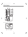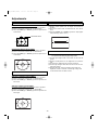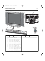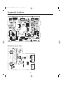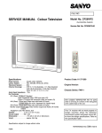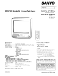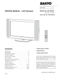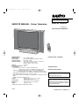
1
SM_29-C8ZRL(Saudi)
10/3/05
10:47 AM
Page 1
FILE NO.
SERVICE MANUAL Colour Television
Model No. CM29FS2
(Saudi/Kuwait)
Service Ref. No. CM29FS2-00
TV/AV
TIMER
?
x
3
2
1
6
5
4
9
8
7
-/--
SOUND
CH
SWAP
P
P
0
i
MENU
A. B
PICTURE
CH
S. SYS SURROUND
TXT/TV
BASS
JXPSB
Specifications
Power Source . . . . . . . .AC110-240V, 50/60Hz.
Colour System . . . . . . . .PAL, SECAM, NTSC4.43, NTSC, PAL 60Hz
Television System . . . . .B/G, D/KK’, I, M/M
Channel Coverage . . . . .VHF: E2-E12, R1-R12, K1-K9, J1-J12, A2-A13
UHF: 21-69, A14-A69, J13-J62
CATV: S1-S41, X, Y, Z, Z+1, Z+2
Video IF . . . . . . . . . . . . . .38.0 MHz
Aerial Input Impedance . 75Ω
Ext. Terminals
Video inputs: Phono jack 2 (1.0Vp-p, impedance 75Ω)
S-Video Input 1 (Din 4 pin, Separate Y/C Signals Input)
DVD Input: Component Video Jack-Y 1 (1.0Vp-p, impedance 75Ω)
Component Video Jack CB/CR 1 (0.7Vp-p, impedance 75Ω)
Audio inputs: Phono jack (R/L) 3 (436mVrms, impedance more than 40KΩ)
Video monitor output: Phono jack 1 (1.0Vp-p, 75Ω)
Audio monitor outputs: Phono jack(R/L) 1(436mVrms, Impedance less than
600Ω)
Headphone jack: Mini Stereo jack 1
Speaker . . . . . . . . . . . . . . Main speaker: 6 cm 12 cm 2 pcs.
Tweeter: ∅5 cm 2 pcs.
Sound Output . . . . . . . . . Main speaker: 7.5W + 7.5W (RMS)
Dimensions . . . . . . . . . . . 803 (W) 578 (H) 418 (D)mm
Weight . . . . . . . . . . . . . . . approx. 47.5 Kg
Specifications subject to change without notice
C8ZRL
Product Code: 111379453
Original Version
Chassis Series: FB1-B
Give complete “SERVICE REF. NO.” for parts
order or servicing. It is shown on the rating plate
at the cabinet back of the unit.
This T.V. receiver will not work properly in
foreign countries where the television
transmission system and power source differ from the design specifications. Refer to
the specification table.
REFERENCE NO.
SM3010120
SM_29-C8ZRL(Saudi)
10/3/05
10:47 AM
Page 2
Contents
Safety Notice . . . . . . . . . . . . . . . . . . . . . . . . . . . . . . . . . . . . . . . . . . . . . . . 2
Chassis Block Diagram . . . . . . . . . . . . . . . . . . . . . . . . . . . . . . . . . . . . . . . 3
IC Block Diagrams . . . . . . . . . . . . . . . . . . . . . . . . . . . . . . . . . . . . . . . . . 4-6
CPU Port Functions . . . . . . . . . . . . . . . . . . . . . . . . . . . . . . . . . . . . . . . . 7-8
Option Setting . . . . . . . . . . . . . . . . . . . . . . . . . . . . . . . . . . . . . . . . . . . . . . 9
Service Adjustments with Replacing Memory IC (IC802) . . . . . . . . . . 10-15
Dealer Mode . . . . . . . . . . . . . . . . . . . . . . . . . . . . . . . . . . . . . . . . . . . . . . .16
Adjustment . . . . . . . . . . . . . . . . . . . . . . . . . . . . . . . . . . . . . . . . . . . . . .17-18
Purity and Convergence Adjustment . . . . . . . . . . . . . . . . . . . . . . . . . 19-20
Mechanical Disassembly . . . . . . . . . . . . . . . . . . . . . . . . . . . . . . . . . . . . . 21
Protection Circuit . . . . . . . . . . . . . . . . . . . . . . . . . . . . . . . . . . . . . . . . . . . 21
Cabinet Parts List . . . . . . . . . . . . . . . . . . . . . . . . . . . . . . . . . . . . . . . . . . 22
Chassis Electrical Parts List . . . . . . . . . . . . . . . . . . . . . . . . . . . . . . . . 23-31
Component Locations . . . . . . . . . . . . . . . . . . . . . . . . . . . . . . . . . . . . . 32-34
Voltages and Waveforms Charts . . . . . . . . . . . . . . . . . . . . . . . . . . . . . 35-36
Safety Notice
SAFETY PRECAUTIONS
1: An isolation transformer should be connected in the
power line between the receiver and the AC line
when a service is performed on the primary of the
converter transformer of the set.
3: When replacing a chassis in the cabinet, always be
certain that all the protective devices are installed
properly, such as, control knobs, adjustment covers
or shields, barriers, isolation resistor-capacitor networks etc.. Before returning any television to the
customer, the service technician must be sure that
it is completely safe to operate without danger of
electrical shock.
2: Comply with all caution and safety-related notes provided on the cabinet back, inside the cabinet, on the
chassis or the picture tube.
X-RADIATION PRECAUTION
The primary source of X-RADIATION in television receiver is the picture tube. The picture tube is specially constructed to limit X-RADIATION emissions. For continued X-RADIATION protection, the replacement tube must be
the same type as the original including suffix letter. Excessive high voltage may produce potentially hazardous X
- RADIATION. To avoid such hazards, the high voltage must be maintained within specified limit. Refer to this
service manual, high voltage adjustment for specific high voltage limit. If high voltage exceeds specified limits,
take necessary corrective action. Carefully follow the instructions for + B1 volt power supply adjustment, and high
voltage check to maintain the high voltage within the specified limits.
PRODUCT SAFETY NOTICE
Product safety should be considered when a component replacement is made in any area of a receiver.
Components indicated by mark
in the parts list and the schematic diagram designate components in which
safety can be of special significance. It is particularly recommended that only parts designated on the parts list
in this manual be used for component replacement designated by mark
. No deviations from resistance
wattage or voltage ratings may be made for replacement items designated by mark
.
-2-
TUNER
INPUT-1
INPUT-2
-3-
INPUT-3
L/R
VIDEO
Cr-IN
Cb-IN
Y-IN
L/R
L/R
VIDEO
VIF/SIF
MONITOR
OUT
H-PHONE
WOOFER
SPEAKER
IC001
AUDIO AMP.
IC1401
WOOFER AMP.
IC201
PROCESSOR
KEY SW
RC
RECEIVER
LED
Q431
H-DRIVE
PCC
CIRCUIT
T431
H-DRIVE
TRANS
IC501
VERTICAL
Q432
H-OUT
T471
FBT
Q901
CRT
10:47 AM
L/R
IC701
TRIPLE
VIDEO
OUTPUT
AMP
10/3/05
VIDEO
Y/C
IC802
EEPROM
SM_29-C8ZRL(Saudi)
Page 3
Chassis Block Diagrams
IC1401<Woofer Pre-Amp. IC> is not used
SOUND MUTE
VIDEO SELECTOR
(LOW=AV1, H=AV2)
-4-
LED
32.768KHz
OSC
X801
CPU OSC OUT
CPU OSC IN
ON-TIMER LED OUT (ON TIMER ON=Low)
RC PRE-AMP.
RC SIGNAL IN
(ACTIVE=HIGH)
VIF-M OUTPUT (HIGH=NTSC, LOW=OTHER)
BILINGUAL OUTPUT (LOW=S-1, HIGH=S-2)
26
7
6
112
99
33
16
9
11
5
SCL
6
IC802
MEMORY
99
SDA
98
17
127
18
106
1
2
12
IC201
QXXAVC534C7JAS
QXXAVC534M
13
122
PHOTO COUPLE
KEY
SWITCH
(POWER ERROR=LOW)
POWER PROTECT IN
A101
F/S TUNER
DEFLECTION
CIRCUIT
5
4
IC3701
AUDIO CONTROL/
SURROUND
13 14
POWER CIRCUIT
etc.
VERT. SYNC IN (ACTIVE=LOW)
HORIZ. SYNC IN (ACTIVE=LOW)
POWER ON/OFF
(ON=HIGH, OFF=LOW)
SDA
SCL
KEY SWITCH IN
COLOUR SYSTEM OPTION INPUT
10:47 AM
SECAM KILLER INPUT (HIGH=SECAM)
2
RESET INPUT (RESET=LOW)
10
10/3/05
IC1201
VIDEO SELECTOR
IC001
AUDIO AMP.
SM_29-C8ZRL(Saudi)
Page 4
IC Block Diagrams
System Control
-5-
52
64
CVBSO/PIP
51
59
58
55
73
48
25
24
31
CVBS2/Y2
CVBS3/Y3
C2/C3
CVBS4/Y4
C4
YSYNC
IFVO/SVO/
CVBSI
VIFIN
AGCOUT
DVBO/FMRO
44
43
30
67
H/V
Y
C
23
32
REF
V-DRIVE
EHTO
EWD
22
GEOMETRY
& EAST-WEST
VERTICAL
Y DELAY ADJ.
COMB FILTER
2H/4H
DIGITAL
DECODER
PAL/SECAM/NTSC
BL
80
Vi
RDS
61
60
62
L
SATURATION
U/V TINT
SKIN TONE
YUV
U/V DELAY
PEAKING
SCAN VELOCITY
MODULATION
G
B
CR
SAT
GAMMA CONTROL
BLACK STRETCH
BLUE STRETCH
RGB MATRIX
RGB CONTROL
OSD/TEXT INSERT
CONTR/BRIGHTN
CCC
BRI
WHITE-P.ADJ.
CON.
BL R
DIGITAL SIGNAL PROCESSING FEATURES
SCAVEM
ON TEXT
63
R
HP-OUT
AUDIO CONTROL
VOLUME
TREBBLE/BASS
FEATURES
DACS
R
L
LS-OUT
µ-PROCESSOR AND TELETEXT DECODER
ADC/DAC
AUDIO SELECT
B/PB
G/Y
R/PR
(CVBSX/YX)(CX)
Vo Uo Yo Yi Ui
76
SWO1 BL
B/PB
79
YUV INTERFACE
G/Y
R/PR
78
AM
RGB/YPRPB INSERT
DELAY LINE
BASE-BAND
DECODER
STEREO
ALL-STANDARD
A/D CONVERTER
YUV IN/OUT
HOUT
H/V SYNC SEP.
H.OSC. + PLL
2nd LOOP
H-SHIFT
H.DRIVE
VIDEO FILTERS
VIDEO IDENT.
VIDEO SWITCH
VISION IF/AGC/AFC
PLL DEMOD.
SOUND TRAP
GROUP DELAY
VIDEO AMP.
DEEMPHASIS
SOUND PLL
SCART/CINCH IN/OUT 12S
65
84
83
87
86
85
SVM
RO
GO
BO
BCLIN
BLKIN
I/OS
10:47 AM
DVBO/IFVO/
FMRO
SIFIN/DVBIN
SWITCH
QSS SOUND IF
AGC
QSS MIXER
AM DEMODULATOR
33
SSIF
10/3/05
29
39
QSSO/AMOUT
REFO
SM_29-C8ZRL(Saudi)
Page 5
IC Block Diagrams
IC201 < CPU/IF/Video/Chroma/Def.> QXXAVC534C7JAS
SM_29-C8ZRL(Saudi)
10/3/05
10:47 AM
Page 6
IC Block Diagrams
IC001 < Audio AMP.> TDA8947J/N3
VCC1
VCC2
16
3
IN1+
8
+
+
+
-
+
-
+
+
1
OUT1+
60 kΩ
IN2+
6
4
OUT2-
60 kΩ
IN3+
9
14
OUT3-
60 kΩ
IN4+
12
17
OUT4+
60 kΩ
CIV
SHORT CIRCUIT
AND
TEMPERATURE
PROTECTION
13
Vcc
SVR
11
0.5Vcc
Vref
SGND
MODE1
MODE2
7
10
STANDBY ALL
MUTE ALL
ON 1+2
5
MUTE 3+4
ON 3+4
TDA8947J
2
15
GND1
GND2
IC501 < Vertical Output > LA78041
Thermal
Protection
AMP
+
5
6
7
NON INV.
INPUT
GND
4
Ver. OUTPUT
3
PUMP UP
OUT
2
Vcc
INVERTING
INPUT
1
OUTPUT
STAGE Vcc
Pump
Up
-6-
SM_29-C8ZRL(Saudi)
10/3/05
10:47 AM
Page 7
CPU Port Functions
Pin No.
Function Name
Function
1
VSSP2
Ground
2
VSSC4
Ground
3
VDDC4
Digital supply to SDACs (1.8V)
4
VDDA3(3.3V)
Supply (3.3V)
5
VREF_POS_LSL
6
VREF_NEG_LSL+HPL
7
Pin No.
Function Name
Function
43
DVBO/IFVO/FMRO (2)
Digital Video Broadcast output / IF
video output / FM radio output
44
DVBO/FMRO
Digital Video Broadcast output / FM
radio output
Positive reference voltage SDAC (3.3V)
45
VCC8V
8 Volt supply for audio switches
Negative reference voltage SDAC (0 V)
46
AGC2SIF
AGC capacitor second sound IF
VREF_POS_LSR+HPR Positive reference voltage SDAC (3.3 V)
47
VP2
2nd supply voltage TV processor (+5 V)
8
VREF_NEG_HPL+HPR Negative reference voltage SDAC (0 V)
48
IFVO/SVO/CVBSI (2)
9
VREF_POS_HPR
Positive reference voltage SDAC (3.3V)
IF video output / selected CVBS
output / CVBS input
10
XTALIN
Crystal oscillator input
49
AUDIOIN4L
Audio-4 input (left signal)
AUDIOIN4R
Audio-4 input (right signal)
(2)
11
XTALOUT
Crystal oscillator output
50
12
VSSA1
Ground
51
CVBS4/Y4
CVBS2/Y4 input
C4
Chroma-4 input
13
VGUARD/SWIO
V-guard input / I/O switch
52
14
DECDIG
Decoupling digital supply
53
AUDIOIN2L/SSIF
15
VP1
1st supply voltage TV-processor (+5 V)
16
PH2LF
Phase-2 filter
54
AUDIOIN2R
Audio 2 input (right signal)
55
CVBS2/Y2
CVBS2/Y2 input
56
AUDIOIN3L
Audio 3 input (left signal)
57
AUDIOIN3R
Audio 3 input (right signal)
58
CVBS3/Y3
CVBS3/Y3 input
59
C2/C3
Chroma-2/3 input
60
AUDOUTLSL
Audio output for audio power amplifier (left signal)
61
AUDOUTLSR
Audio output for audio power amplifier (left signal)
62
AUDOUTHPL
Audio output for headphone channel
(left signal)
63
AUDOUTHPR
Audio output for headphone channel
(Right signal)
17
PH1LF
Phase-1 filter
18
GND1
Ground 1 for TV-processor
19
SECPLL
SECAM PLL decoupling
20
DECBG
Bandgap decoupling
21
EWD/AVL (1)
East-West drive output or AVL capacitor
22
VDRB
Vertical drive B output
23
VDRA
Vertical drive A output
24
VIFIN1
IF Input 1
25
VIFIN2
IF Input 2
26
VSC
Vertical sawtooth capacitor
27
IREF
Reference current input
28
GNDIF
Ground connection for IF amplifier
29
SIFIN1/DVBIN1 (2)
SIF input 1 / DVB input 1
30
SIFIN2/DVBIN2 (2)
SIF input 2 / DVB input 2
31
AGCOUT
Tuner AGC output
32
EHTO
33
AVL/SWO/SSIF/
(2)(3)
REFO/REFIN
(3)
Audio 2 input (left signal) / sound IF
input
64
CVBSO/PIP
CVBS / PIP output
65
SVM
Scan velocity modulation output
66
FBISO/CSY
Flyback input/sandcastle output or
composite H/V timing output
EHT/overvoltage protection input
67
HOUT
Horizontal output
Automatic Volume Levelling / swith
output / sound IF input / subcarier
reference output / external reference
signal input for I signal mixer for
DVB operation
68
VSScomb
Ground connection for comb filter
69
VDDcomb
Supply voltage for comb filter (5V)
70
VIN (R/PRIN2/CX)
V-input for YUV interface (2nd R
input / PR input or Cx input)
Audio-5 input (left signal)
71
UIN (B/PBIN2)
U-input for YUV interface (2nd B
input / PB input)
72
YIN (G/YIN2/CVBS-Yx) Y-input for YUV interface (2nd G
input / Y input or CVBS/Yx input)
73
YSYNC
74
YOUT
Y-output (for YUV interface)
75
UOUT (INSSW2)
U-output for YUV interface (2nd
RGB / YPBPR insertation input)
76
VOUT (SW01)
V-output for YUV interface (general
purpose switch output)
77
INSSW3
3rd RGB / YPBPR insertion input
78
R/PRIN3
3rd R input / PR input
34
AUDIOIN5L
35
AUDIOIN5R
Audio-5 input (right signal)
36
AUDOUTSL
Audio output for SCART/CINCH (left signal)
37
AUDOUTSR
Audio output for SCART/CINCH (right signal)
38
DECSDEM
Decoupling sound demodulator
39
QSSO/AMOUT
/AUDEEM (2)
QSS intercarrier output / AM output
/ deemphasis (front-end audio out)
40
GND2
Ground 2 for TV processor
41
PLLIF
IF-PLL loop filter
42
SIFAGC/DVBAGC(2) AGC sound IF / internal-external
AGC for DVB applications
-7-
Y-input for sync separator
SM_29-C8ZRL(Saudi)
10/3/05
10:47 AM
Page 8
CPU Port Functions
Pin No.
Function Name
Function
G/YIN3
3rd G input / Y input
80
B/PBIN3
3rd B input / PB input
81
GND3
Ground 3 for TV-processor
82
VP3
3rd supply for TV processor (5V)
83
BCLIN
Beam current limiter input
79
84
BKLIN
Black current input
85
RO
Red output
86
GO
Green output
87
BO
Blue output
88
VDDA1
Analog supply for TCG µ-Controller
and digital supply for TV-processor
(+3.3V)
89
VREFAD_NEG
Negative reference voltage (0 V)
90
VREFAD_POS
Positive reference voltage (3.3 V)
91
VREFAD
Reference voltage for audio ADCs
(3.3/2 V)
92
GNDA
Ground
93
VDDA(1.8V)
Analogue supply for audio ADCs
(1.8V)
94
VDDA2(3.3)
Supply voltage SDAC (3.3 V)
95
VSSadc
Ground for video ADC and PLL
96
VDDadc(1.8)
Supply voltage video ADC and PLL
97
INT0/P0.5
External interrupt 0 or port 0.5 (4 mA
current sinking capability for direct
drive of LEDs)
98
P1.0/INT1
Port 1.0 or external interupt 1
99
P1.1/T0
Port 1.1 or Counter/Timer 0 input
100
VDDC2
Digital supply to core (1.8 V)
101
VSSC2
Ground
102
P0.4/I2SWS
Port 0.4 or I2S word select
103
P0.3/I2SCLK
Port 0.3 or I2S clock
104
P0.2/I2SDO2
Port 0.2 or I2S digital output 2
105
P0.1/I2SDo1
Port 0.1 or I2S digital output 1
106
P0.0/I2SDI1/O
Port 0.0 or I2S digital input 1 or I2S
digital output
107
P1.3/T1
Port 1.3 or Counter/Timer 1 input
108
P1.6/SCL
Port 1.6 or I2C-bus clock line
109
P1.7/SDA
Port 1.7 or I2C-bus data line
110
VDDP(3.3V)
Supply to periphery and on-chip voltage
regulator (3.3V)
111
P2.0/TPWM
Port 2.0 or Tuning PWM output
112
P2.1/PWM0
Port 2.1 or PWM0 output
113
P2.2/PWM1
Port 2.2 or PWM1 output
114
P2.3/PWM2
Port 2.3 or PWM2 output
115
P3.0/ADC0
Port 3.0 or ADC0 input
116
P3.1/ADC1
Port 3.1 or ADC1 input
117
VDDC1
Digital supply to core (+1.8V)
118
DECV1V8
Decoupling 1.8V supply
119
P3.2/ADC2
Port 3.2 or ADC2 input
Pin No.
-8-
Function Name
Function
120
P3.3/ADC3
Port 3.3 or ADC3 input
121
VSSC/P
Digital ground for µ-Controller core
and periphery
122
P2.4/PWM3
Port 2.4 or PWM3 output
123
P2.5/PWM4
Port 2.5 or PWM4 output
124
VDDC3
Digital supply to core (1.8V)
125
VSSC3
Ground
126
P1.2/INT2
Port 1.2 or external interrupt 2
127
P1.4/RX
Port 1.4 or UART bus
128
P1.5/TX
Port 1.5 or UART bus
SM_29-C8ZRL(Saudi)
10/3/05
10:47 AM
Page 9
Option Setting
After replacing the Memory IC (IC802)
The memory IC (IC802), stores the option data of TV set and service adjustments data for each circuit, therefore,
when the memory IC is replaced, it should be programmed to the following settings and “ SERVICE ADJUSTMENT”
on pages 15 to 16.
1) To enter to the Option Mode
Press and hold the MENU on the remote control and Programme down button (CH) on the front panel of
the TV. The option window will appear on the screen.
MENU
OPTION
PLUG & PLAY
WELCOME TEXT
AUTO VOLUME
TEXT NO SIGNAL
AFC
ON
OFF
OFF
ON
ON
Option Mode
TV/AV
MENU
-
+
CH
HOTEL MODE
OFF
2) To set the Option Mode
Select the desired option item by pressing the Programme down or up button.
To switch the option mode, use the Level up or down button.
The data which is set in the option mode is stored into the memory IC automatically.
The following table shows the available option items and default setting mode.
Option Mode
Mode
Description & Note
PLUG & PLAY
WELCOME TEXT
AUTO VOLUME
TEXT NO SIGNAL
AFC
ON
ON
ON
ON
ON
Plug & Play mode, default “ON”
Display message when first set up, default “OFF”
Auto volume, default “OFF”
When no received signal, execution, default “ON”
Automatic Frequency Control (AFC) available, default “ON”
or
or
or
or
or
OFF
OFF
OFF
OFF
OFF
3) Exit from the Service Mode
Press the Menu button or turn off the TV set by using the mains switch.
-9-
SM_29-C8ZRL(Saudi)
10/3/05
10:47 AM
Page 10
Service Adjustments with Replacing Memory IC(IC802)
Note: The CPU (IC201) and memory IC (IC802) store the service adjustments data and controls data for each
circuit.When the Memory IC(IC802) is replaced, some of the service adjustments should be readjusted to
obtain the best performance. The necessary service adjustments are carried out by using the RC handset.
Please set up the TV set with following steps [1] to [2].
[1] Initializing Procedure
1. Put a new memory IC.
2. Turn on the TV set.
3. Enter to the Service Mode as explanation on next page. Select “002 INIT TV 0” mode, then change to “1” by
pressing Volume + button on Remote Control.
4. When initialised the memory IC are completed, TV set will in stand by mode, all of the setting data (option data and
service adjustment data) stored in the IC are reset to the default value. It is necessary to set the option settings and
readjust the service adjustments (listed on page 11-13) and to re-tune all the channels.
This completes the initialization of memory IC.
Following shows the initialized contents of memory data by this procedure.
- Plug & Play
: No executed
- Inhibit Data
: Cancelled
- Ch Skip Data
: Cancelled
- Swap Data
: Cancelled
- Surround
: OFF
- Woofer
: OFF
- Sound Volume Data
: 12/63 steps
- Bass Data
: 32/63 steps
- Treble Data
: 32/63 Steps
- Colour System
: AUTO
- Sound System
: BG
[2] Required Service Adjustments
Readjust the following service adjustments.
Adjustments
Service Mode No. & Item
Vertical slope
Item 015, Vert. Slope
Vertical shift
Item 016, Vert. Shift
Vertical amplitude
Item 017, Vert. Ampl.
Vertical-S correction
Item 018, S-Corr.
EW width
Item 021, EW Width
Horizontal shift
Item 022, Hor. Shift
----Further adjustment please refer to page 12 ~ 14.
-10-
SM_29-C8ZRL(Saudi)
10/3/05
10:47 AM
Page 11
Service Adjustments with Replacing Memory IC(IC802)
1) To enter to the Service Mode
1. Press and hold the Volume + button on the front of TV set and press the Menu button on the Remote Control.
Display for Software Version Information
TV/AV
MENU
-
+
CH
SERVICE
001 FB1B
0.92
MENU
MENU
2. Press the Programme up / down button to select the mode required. Then press the Volume + button to
adjust.
CH
9695949392....01..
0102030405....96..
CH
Example
Display for [V.Linearity] Vertical Linearity adjustment
Item No.
ZOOM 50HZ
020 V.LINEARITY
00111010
01010000
10000001
00011010
39
00000000
10001100
00001010
00001010
Read Status
Item
Adjustment Data
3) Exit from the Service Mode
Press the Menu button or turn off the TV set by using the mains switch.
-11-
SM_29-C8ZRL(Saudi)
10/3/05
10:47 AM
Page 12
Service Adjustments with Replacing Memory IC(IC802)
Following table shows the initial values which have been stored in the CPU ROM, and items for the service adjustments.
Service mode adjustments table in CPU ROM
No.
ITEM
DATA INITIAL
RANGE SETUP
DATA
0.3
DESCRIPTION
No.
ITEM
Software version information
46
Z4 VX
01 FB1C/FB1B
x,y
02
Init TV
0 -1
0
Initialise NVM
47
Z4 PW
03
ISP Mode
0-1
0
Set the TV in ISP mode
48
Z4 UCP
0 - 255
DESCRIPTION
11
Zoom 14:9 Vertical Zoom (50Hz)
0 - 255
2
Zoom 14:9 Parabola/Width (50Hz)
0 - 255
4
Zoom 14:9 Upper Corner Parabola (50Hz)
04
PWT
-
05
DDLE
0-1
06
Cut Off
0 - 63
42
07
VSD
On/Off
000
08
VG2
On/Off
000
Adjustment Vg2 voltage
53
T4 PW
0 - 255
0
Title In 14:9 Parabola/Width (50Hz)
10
DCXO
0 - 127
48
DXCO adjustment
54
T4 UCP
0 - 255
2
Title In 14:9 Upper Corner Parabola (50Hz)
On/Off
000
11 DXCO Auto
00000 Power on time
DATA INITIAL
RANGE SETUP
DATA
49
Z4 LCP
0 - 255
255
Zoom 14:9 Lower Corner Parabola (50Hz)
50
Z4 VSC
0 - 255
248
Zoom 14:9 Vertical Scroll (50Hz)
Cut off
51
T4 VX
0 - 255
0
Title In 14:9 Vertical Zoom (50Hz)
Vertical scan disable (1 line adj.)
52
T4 VS
0 - 255
127
Title In 14:9 Vertical Slope (50Hz)
1
Automatic DXCO adjustment
55
T4 LCP
0 - 255
252
(Adjust in NICAM)
56
T4 VSC
0 - 255
7
Title In 14:9 Vertical Scroll (50Hz)
Title In 14:9 Lower Corner Parabola (50Hz)
12
TUBE-TYPE
0-1
1
Picture tube type (0=16:9, 1=4:3)
57
Z6 VX
0 - 255
21
Zoom 16:9 Vertical Zoom (50Hz)
13
OP WIDE ZOOM
0-1
0
0=No Zoom mode, 1=with zoom mode
58
Z6 PW
0 - 255
0
Zoom 16:9 Parabola/Width (50Hz)
14
TRACK. MODE
0-1
0
Track. Mode (HCO)
59
Z6 UCP
0 - 255
0
Zoom 16:9 Upper Corner Parabola (50Hz)
15
VERT. ZOOM
0 - 63
27
Vertical Zoom
60
Z6 LCP
0 - 255
253
Zoom 16:9 Lower Corner Parabola (50Hz)
16
VERT. SLOPE
0 - 63
35
Vertical Slope
61
Z6 VSC
0 - 255
0
Zoom 16:9 Vertical Scroll (50Hz)
17 VERT. SHIFT 0 - 63
30
Vertical Shift
62
T6 VX
0 - 255
8
Title In 16:9 Vertical Zoom (50Hz)
18 VERT. AMPL. 0 - 63
30
Vertical Amplitude
63
T6 VS
0 - 255
4
Title In 16:9 Vertical Scroll (50Hz)
19
32
S-Correction
64
T6 PW
0 - 255
0
Title In 16:9 Parabola/width (50Hz)
S-CORR
20 V.LIN.CTRL
0 - 63
0-2
0
Vertical Linearity Control
65
T6 UCP
0 - 255
2
Title In 16:9 Upper Corner Parabola (50Hz)
21 V. LINEARITY 0 - 63
30
Vertical Linearity
66
T6 LCP
0 - 255
253
Title In 16:9 Lower Corner Parabola (50Hz)
22 EW WIDTH
0 - 63
36
East West Width
67
T6 VSC
0 - 255
7
Title In 16:9 Vertical Scroll (50Hz)
23
HOR. SHIFT
0 - 63
30
Horizontal Shift
68
NO VX
0 - 255
0
Normal Vertical Zoom (50Hz)
24
EW PARABOLA
0 - 63
35
East West Parabola Width
69
NO EWW
0 - 255
241
25
TRAPEZIUM
0 - 63
10
East West Trapezium
70
NO HSH
0 - 255
2
Normal Horizontal Shift (50Hz)
26 UC PARABOLA 0 - 63
40
East West Upper Corner Parabola
71
NO PW
0 - 255
0
Normal Parabola/Width (50Hz)
27 LC PARABOLA 0 - 63
45
East West Lower Corner Parabola
72
NO UCP
0 - 255
255
Normal Upper Corner Parabola (50Hz)
Normal EW Width (50Hz)
28 HOR. BOW 0 - 63
35
Horizontal Bow
73
NO LCP
0 - 255
252
29 PARALLEL
0 - 63
37
Horizontal Parallelogram
74
NO VSC
0 - 255
0
Normal Vertical Scroll (50Hz)
30 VERT. SCROLL 0 - 63
32
Vertical Scroll
75
NO HBL
0-1
1
Normal RGB Blanking Mode (50Hz)
31 H BLK SW
1
R G B Blanking Mode
76
NO WBF
0 - 255
0
Normal Timing of Wide Blanking Front
(WBF) 50Hz
77
NO WBR
0 - 255
26
Normal Timing of Wide Blanking Front
(WBF) 50Hz
78 SQ OSVE
0-1
0
Black Current Measuring Lines in
Overscan (50Hz)
0
Extended Vertical Blanking (50Hz)
0-1
Normal Lower Corner Parabola (50Hz)
32
WBF
0 - 15
7
Timing of wide blankingfront(WBF)
33
WBR
0 - 15
10
Timing of wide blanking rear(WBR)
34
OSVE
0-1
0
Black current measuring lines in overscan
35
EVB
0-1
0
Extended Vertical Blanking
36
NA VX
0 - 255
4
Natural Vertical Zoom (50Hz)
79
SQ EVB
0-1
37
NA EWW
0 - 255
6
Natural EW Width (50Hz)
80
I01 TRACK MODE.
0-1
0
Track Mode(HCO)
38
NA HSH
0 - 255
0
Natural Horizontal Shift (50Hz)
81 I02 VERT.ZOOM 0 - 255
1
Vertical Zoom
39
NA PW
0 - 255
3
Natural Parabola/Width (50Hz)
82 I03 VERT.SLOPE 0 - 255
255
Vertival Slope
40
NA TP
0 - 255
251
Natural Trapezium (50Hz)
83 I04 VERT.SHIFT 0 - 255
5
Vertical Shift
41
NA UCP
0 - 255
4
Natural Upper Corner Parabola (50Hz)
84 I05 VERT.AMPL. 0 - 255
1
Vertical Amplitudo
42
NA LCP
0 - 255
1
Natural Lower Corner Parabola (50Hz)
85 I06 S-CORR 0 - 255
0
S-Correction
43
NA HB
0 - 255
253
44
NA HP
0 - 255
45
NA VSC
0 - 255
Natural Horizontal Bow (50Hz)
86 I07 V.LIN.CTRL. 0 - 255
0
Vertical Linearity Control
0
Natural Horizontal Paralellogram (50Hz)
87 I08 V. LINEARITY 0 - 255
8
Vertical Linearity
0
Natural Vertical Scroll (50Hz)
88 I09 EW WIDTH 0 - 255
1
East West Width
-12-
SM_29-C8ZRL(Saudi)
10/3/05
10:47 AM
Page 13
Service Adjustments with Replacing Memory IC(IC802)
Following table shows the initial values which have been stored in the CPU ROM, and items for the service adjustments.
Service mode adjustments table in CPU ROM
No.
ITEM
DATA INITIAL
RANGE SETUP
DATA
89 I10 HOR. SHIFT 0 - 255
90 I11 EW PARABOLA 0 - 255
91
I12 TRAPEZIUM
0 - 255
92
I13 UC PARABOLA
0 - 255
93
I14 LC PARABOLA
0 - 255
94
I15 HOR. BOW
0 - 255
95
I16 PARALEL
0 - 255
96
117 VERT. SCROLL
5
2
DATA INITIAL
RANGE SETUP
DATA
DESCRIPTION
No.
ITEM
Horizontal Shift
133
T6 VSC
0 - 255
NO VX
DESCRIPTION
12
Title In 16:9 Vertical Scroll (50Hz)
Normal Vertical Zoom (50Hz)
East West Parabola Width
134
0 - 255
0
East West Trapezium
135 NO EWW
0 - 255
245
Normal EW Width (50Hz)
0
East West Upper Corner Parabola
136 NO HSH
0 - 255
255
Normal Horizontal Shift (50Hz)
0
East West Lower Corner Parabola
137
0 - 255
3
Normal Parabola/Width (50Hz)
3
Horizontal Bow
138 NO UCP
0 - 255
0
Normal Upper Corner Parabola (50Hz)
0
Horizontal Parallelogram
139
NO LCP
0 - 255
0
Normal Lower Corner Parabola (50Hz)
252
NO PW
0 - 255
0
Vertical Scroll
140
NO VSC
0 - 255
0
Normal Vertical Scroll (50Hz)
97 l18 H BLK SW
0-1
1
RGB Blanking Mode (60Hz)
141
NO HBL
0-1
1
Normal RGB Blanking Mode (50Hz)
98 l19 H BLK L
0 - 255
142 NO WBF
0 - 255
3
Normal Timing of Wide Blanking Front
(WBF) 50Hz
254
Timing of wide blanking front(WBF) 60Hz
99 l20 H BLK R 0 - 255
3
Timing of wide blankingRear(WBF) 60Hz
100 l21 OSVE
0-1
0
Black Current Measuring Lines in
overscan (60Hz)
143 NO WBR
0 - 255
1
Normal Timing of Wide Blanking Front
(WBR) 50Hz
101
l22 EVB
0-1
1
Extended Vertical Blanking
144 SQ OSVE
0-1
0
Black Current Measuring Lines in
Overscan (50Hz)
102
NA VX
0 - 255
5
Natural Vertical Zoom (60Hz)
103 NA EWW
0 - 255
6
Natural EW Width (60Hz)
104
NA HSH
0 - 255
251
Natural Horizontal Shift (60Hz)
105
NA PW
0 - 255
1
Natural Parabola/Width (60Hz)
106
NA TP
0 - 255
1
Natural Trapezium (60Hz)
107
NA UCP
0 - 255
0
Natural Upper Corner Parabola (60Hz)
108
NA LCP
0 - 255
5
Natural Lower Corner Parabola (60Hz)
109
NA HB
0 - 255
0
Natural Horizontal Bow (60Hz)
110
NA HP
0 - 255
0
Natural Horizontal Paralellogram (60Hz)
111
NA VSC
0 - 255
0
Natural Vertical Scroll (60Hz)
112
Z4 VX
0 - 255
10
Zoom 14:9 Vertical Zoom (60Hz)
113
Z4 PW
0 - 255
0
Zoom 14:9 Parabola/Width (60Hz)
114
Z4 UCP
0 - 255
254
Zoom 14:9 Upper Corner Parabola (60Hz)
115
Z4 LCP
0 - 255
2
Zoom 14:9 Lower Corner Parabola (60Hz)
116
Z4 VSC
0 - 255
0
Zoom 14:9 Vertical Scroll (60Hz)
117
T4 VX
0 - 255
4
Title In 14:9 Vertical Zoom (60Hz)
118
T4 VS
0 - 255
3
Title In 14:9 Vertical Slope (60Hz)
119
T4 PW
0 - 255
1
Title In 14:9 Parabola/Width (60Hz)
120
T4 UCP
0 - 255
0
Title In 14:9 Upper Corner Parabola (60Hz)
121
T4 LCP
0 - 255
0
Title In 14:9 Lower Corner Parabola (60Hz)
122
T4 VSC
0 - 255
7
Title In 14:9 Vertical Scroll (60Hz)
123
Z6 VX
0 - 255
12
Zoom 16:9 Vertical Zoom (60Hz)
124
Z6 PW
0 - 255
0
Zoom 16:9 Parabola/Width (60Hz)
125
Z6 UCP
0 - 255
254
Zoom 16:9 Upper Corner Parabola (60Hz)
126
Z6 LCP
0 - 255
1
Zoom 16:9 Lower Corner Parabola (60Hz)
127
Z6 VSC
0 - 255
5
Zoom 16:9 Vertical Scroll (60Hz)
128
T6 VX
0 - 255
10
Title In 16:9 Vertical Zoom (60Hz)
129
T6 VS
0 - 255
1
Title In 16:9 Vertical Scroll (60Hz)
130
T6 PW
0 - 255
0
Title In 16:9 Parabola/width (60Hz)
131
T6 UCP
0 - 255
0
Title In 16:9 Upper Corner Parabola (60Hz)
132
T6 LCP
0 - 255
0
Title In 16:9 Lower Corner Parabola (60Hz)
(WBF) 50Hz
145
SQ EVB
0-1
0
Extended Vertical Blanking (50Hz)
146
CL
0 - 15
13
Cathode Drive Level
148
EVG
On/Off
000
Enable vertical Guard
149
DFL
Active/Disable 000
150
FBC
0-1
151
XDT
Protection/Detection
152
Fixed Beam Current
000 X-Ray Detection
0-1
0
0=Picture Rot. N/A, 1=Pict. Rot. Availabe
153
RGB
0 - 15
10
OSD RGB Brightness For Normal M o d e
154
WPR-N
0 - 63
20
White Point R For Normal (Not Secam)
155
WPG-N
0 - 63
20
White Point G For Normal (Not Secam)
OP PICTROTATION
156
WPB-N
0 - 63
20
White Point B For Normal (Not Secam)
157
BLOR-N
0 - 63
32
Black Level Offset R For Normal (Not Secam)
Black Level Offset G For Normal (Not Secam)
158
BLOG-N
0 - 63
32
159
WPR-S
0 - 255
0
160
WPG-S
0 - 255
0
White Point G For Secam
161
WPB-S
0 - 255
0
White Point B For Secam
162
BLOR-S
0 - 255
0
Black Level Offset R For Secam
163
BLOG-S
0 - 255
0
Black Level Offset G For Secam
164
WPR-D
0 - 255
252
White Point R for DVD Input
165
WPG-D
0 - 255
252
White Point G for DVD Input
166
WPB-D
0 - 255
253
White Point B for DVD Input
167
BLOR-D
0 - 255
0
168
BLOG-D
0 - 255
226
Black Level Offset G for DVD Input
0 - 255
15
RF PAL/NTSC Offset
169 BR RF PN
White Point R For Secam
Black Level Offset R for DVD Input
170
BR AV
0 - 255
16
AV PAL/NTSC Offset
171
BR DVD
0 - 255
10
DVD PAL/NTSC Offset
172
BR S
173 CN RF PN
-13-
0
Disable Flash Protection
0 - 255
16
Secam Offset
0 - 255
248
RF PAL/NTSC Offset
174
CN AV
0 - 255
255
AV PAL/NTSC Offset
175
CN DVD
0 - 255
255
DVD PAL/NTSC Offset
176
CN S
0 - 255
253
Secam Offset
SM_29-C8ZRL(Saudi)
10/3/05
10:47 AM
Page 14
Service Adjustments with Replacing Memory IC(IC802)
Following table shows the initial values which have been stored in the CPU ROM, and items for the service adjustments.
Service mode adjustments table in CPU ROM
No.
ITEM
177
CN 43
DATA INITIAL
RANGE SETUP
DATA
0 - 255
250
DESCRIPTION
Wide Mode 4:3 Offset
178 SH RF PN
0 - 255
10
RF PAL/NTSC Offset
179
SH AV
0 - 255
10
AV PAL/NTSC Offset
180
SH DVD
0 - 255
10
DVD PAL/NTSC Offset
181
SH S
0 - 255
10
Secam Offset
182 CL RF P
0 - 255
5
RF PAL/NTSC Offset
183
CL AVP
0 - 255
5
AV PAL Offset
184
CL N
0 - 255
0
NTSC RF/Video Offset
185
CL S
0 - 255
0
Secam Offset
186
CL DVD
0 - 255
7
DVD PAL/NTSC Offset
187
CL 43
0 - 255
0
Wide Mode 4:3 Offset
188 PV-BR-DY
0 - 63
31
Preset Video Dynamic Brightness
189 PV-CT-DY
0 - 63
63
Preset Video Dynamic Contrast
190 PV-CL-DY
0 - 63
36
Preset Video Dynamic Colour
191 PV-SH-DY
0 - 63
54
Preset Video Dynamic Sharpness
192 PV-BR-ST
0 - 63
32
Preset Video Standard Brightness
193 PV-CT-ST
0 - 63
50
Preset Video Standard Contrast
194 PV-CL-ST
0 - 63
32
Preset Video Standard Colour
195 PV-SH-ST
0 - 63
35
Preset Video Standard Sharpness
196 PV-BR-EC
0 - 63
31
Preset Video Eco Brightness
197 PV-CT-EC
0 - 63
40
Preset Video Eco Contrast
198 PV-CL-EC
0 - 63
26
Preset Video Eco Colour
199 PV-SH-EC
0 - 63
31
Preset Video Eco Sharpness
200 PV-BR-GA
0 - 63
36
Preset Video Game Brightness
201 PV-CT-GA
0 - 63
25
Preset Video Game Contrast
202 PV-CL-GA
0 - 63
36
Preset Video Game Colour
203 PV-SH-GA
0 - 63
31
Preset Video Game Sharpness
204
CLO S
0-1
0
205
DTR S
0-1
0
206 Y-SECAM
0 - 15
11
Y-Delay Adjusment for SECAM
207
YNTSC
0 - 15
6
Y-Delay Adjusment for NTSC
208
YPAL
0 - 15
4
Y-Delay Adjustment for PAL
209
YAV
0 - 15
4
Y-Delay Adjustment for AV
211
YSVHS
0 - 15
4
Y-Delay Adjustment for S-VHS
212
ACL
On/Off
000
213
MUS
Japan
1
NTSC Matrix
214 PWL CONTROL On/Off
0
Peak White Limiting On/Off Control
215
PWL
0 - 15
8
Peak White Limiting DAC Control
216
CB
On/Off
1
Chroma Bandpass Centre Freq.
On/Off
0
CB Setting for RF PAL
218 CB AV N
On/Off
0
CB Setting for AV NTSC
219
On/Off
1
Control Sequence Beam Current Limiting
220
CBS
BSD
On/Off
1
BPS
On/Off
000
Bypass Chroma Base-Band
222
FCO
On/Off
000
Forced Colour On
223
224
SVMA
SVM
226
DATA INITIAL
RANGE SETUP
DATA
0-1
1
00 ns
00
25 ns
50 ns
75 ns
100 ns
125 ns
150 ns
175 ns
VMA
Off
2
0.8 Vp-p
1.2 Vp-p
1.8 Vp-p
SMD
Off
1
Video
TXT/OSD
Video/OSD
SVM-OSD-PW
0-3
3
SMD-OSD-TM
0 -7
2
PeakFreq PAL443 0 - 3
3
PeakFreqAV
0 -3
3
227
228
229
230
231 SoftClipevel
0% above PWL 000
DESCRIPTION
Scavem Output Signal
Delay of RGB output to SVM output
Amplitude of SVM output
Scan Velocity Modulation Mode
OSD Scavem Pulse Width
OSD Scavem Time
No Function. Peaking Centre Frequency
Peaking Centre Frequency Default
Soft Cliping Level
5% above PWL
10% above PWL
Off
232
BLUE BACK MUTE
0=Off
0
Blue Back Mute
1=Black Back
2=Blue Back
233 TXT MAX
234 TXT CEN
0 - 15
0 - 15
15
8
235 TXT MIN
236 Blackstretch
0 - 15
0-1
0
1
237 Bluestretch
0-1
000
238 Whitestretch
0-3
3
OSD RGB Brightness for TEXT BRIGHTNESS MAX
OSD RGB Brightness for TEXT BRIGHTNESS
CENTER
239 SoftClipper
0-3
000
240 PeakRatio0VShot 0 - 3
3
241 Tint Def
0 - 63
32
242 Tint NT
0 - 255
0
243
OSO
On/Off
1
244
FSL Noise Detector 60% 000
245
HP2
0-1
000
246 MR VOL L 0 - 255
247 MR VOL H
0-7
248 EQU_SUB_BASS 0 - 63
249 EQU_SUB_TREBLE 0 - 63
250 OP AUDIO CONFIG 0 - 2
OSD RGB Brightness for TEXT BRIGHTNESS MIN
Black Stretch Functionality
(0=Disable, 1=Enable)
Blue Stretch Functionality
(0=Disable, 1=Enable)
White Stretch Setting
(0=cold, 1=normal, 2=warm, 3=)
Set Soft Clipper
Set Peaking Ratio
Default Tint Value
Switch-Off in Vertical Overscan
Forced Slicing Level for Vertical sync
Synchronisation of OSD/TEXT display
(0=Phi 1, 1=Phi 2)
52
4
Master Volume Lower 8 bits
Master Volume Upper 3 bits
31
Equalizer Adjustment for Bass
38
Equalizer Adjustment for Treble
2
0=Mono only functions. 1=No Audio SSD available Audio SSD functions available but no
stereo decoder. 2=Full Audio SSD
253
254
255
Black Stretch Depth
221
ITEM
225
Automatic Colour Limiting
217 CB RF P
No.
OP MONOURAL
0-1
0
0=AV Stereo, 1=Mono.
OP BASS EXP
0-1
1
0=No Bass Exp./Woofer, 1=with Bass Exp./Woofer
OP WOOFER
0-1
0
Activated/Deactivated Bass Expander Feature
Menu. (0=Bass Expander, 1=Woofer)
-14-
SM_29-C8ZRL(Saudi)
10/3/05
10:47 AM
Page 15
Service Adjustments with Replacing Memory IC(IC802)
Following table shows the initial values which have been stored in the CPU ROM, and items for the service adjustments.
Service mode adjustments table in CPU ROM
No.
ITEM
256 OP SURROUND
DATA INITIAL
RANGE SETUP
DATA
0-1
1
257 OP MPP
0-1
0
258
0-1
1
260
261
262
263
264
265
266
267
268
269
270
271
272
273
274
275
276
277
278
279
280
281
282
283
284
285
286
287
288
289
290
291
292
293
294
295
296
297
298
299
300
301
302
303
OP EQUALIZER
AVL-LRF
AVL-LAV
AVL-WGT
AVL-MOD
DVB-CA
DVB-CL
DVB-CH
OP-CLIP
DEC-LEV
FFI
PA-BA-MU
PA-TR-MU
PA-B1-MU
PA-B2-MU
PA-B3-MU
PA-B4-MU
PA-B5-MU
PA-BA-TA
PA-TR-TA
PA-B1-TA
PA-B2-TA
PA-B3-TA
PA-B4-TA
PA-B5-TA
PA-BA-NO
PA-TR-NO
PA-B1-NO
PA-B2-NO
PA-B3-NO
PA-B4-NO
PA-B5-NO
DSG
FMWS
AGN
CV2
0 - 15
0 - 15
0-1
0-5
0 - 255
0 - 255
0 - 15
0-4
0 - 31
0 - 31
0 - 31
0 - 31
0 - 31
FE
AV
0-1
0 - 63
0 - 63
0 - 63
0 - 63
0 - 63
0 - 63
0 - 63
0 - 63
0 - 63
0 - 63
0 - 63
0 - 63
0 - 63
0 - 63
0 - 63
0 - 63
0 - 63
0 - 63
0 - 63
0 - 63
0 - 63
0-1
0-3
0-1
0-1
OVMADAPT
0-1
MONO-LEV
NIC-LEV
ADC-AM-L
ADC-AV-L
E2D
OVMTHR
0 - 15
ASD SC1 THR 0 - 31
CHSE
0-3
9
5
1
2
000
000
8
000
15
15
16
15
15
000
DESCRIPTION
No.
Activated / Deactivated Surround
feature. (0=No Surround, 1=with
Surround.)
Activated / Deactivated MPP
feature. (0=No MPP, 1=with MPP.)
Activated / Deactivated Equalizer
Menu. (0=No Equalizer, 1=with
Equalizer.)
AVL Weight
AVL Delay Time
ITEM
DATA INITIAL
RANGE SETUP
DATA
305 AGC Speed
0-3
1
306
AGC Take Over
0 - 63
26
307
OIF
0 - 63
32
308
IF
0-7
3
PLL Demodulator Frequency
309
GD
0-1
0
Group Delay CVBS1
310
IFO
0-7
0
Set Condition IFV0 Pin4344
314
AKB
On/Off
000
Black Currennt Stabilisation
315
OP TELETEXT
0-1
1
327 PMUTE AKB 0 - 255
40
328 PMUTE DEF 0 - 255
15
329
SVO
IF / CVBS 1
330
BPB
0-1
000
331 OP DVD INPUT 0 - 1
1
332 OP WSS 4:3 MODE 0 - 1
1
Clip Management
FM Stereo decoder output level adjust
Mono Output Level Adjust
Nicam Output Level Adjust
External AM Level Adjust
External AV Level Adjust
DESCRIPTION
IF AGC Speed
AGC Take Over also used as TOP
when an internal AGC tuner is used.
Correction for DC Offset in the IF-PLL
Activated / Deactivated Teletext
features (0=No Teletext, 1=with.)
Selected Video Output
Bypass Internal Sound Bandpass Filter
(0=No DVD Input, 1=with DVD Input.)
Option Zoom Mode (Auto Position) if there is
no WSS or no scart middle voltage. (0=No
WSS, Natural Wide, 1=No WSS, Normal Wide.)
333
OP SCART INPUT
0-2
0
0 - 63
6
(0=No Scart Input, 1=with 1 Scart Input, 2=with 2
Scart Input.)
334 TXT-H-POS
Selection of Audio Output Signal on AUDEEM pin
Option Zoom Mode (Auto Position) if
there is no WSS or no Scart middle Voltage
000
56
46
63
47
32
47
63
20
56
32
42
52
42
32
32
32
32
32
32
32
32
1
1
000
0
338 OSVE AV
0-1
347
NLEL
0 - 255
348
NUEL
0 - 255
349 L HI CUT
0 - 63
350 TEXT EW OFFSET 0 - 255
351 INH EW OFFSET 0 - 255
352 OPTION SVM MENU 0 - 1
Fast Filter IF-PLL
Preset Audio Bass Music
Preset Audio Treble Music
Preset Audio Equalizer Band 1 (100Hz) Music
Preset Audio Equalizer Band 2 (300Hz) Music
Preset Audio Equalizer Band 3 (1000Hz) Music
Preset Audio Equalizer Band 4 (3000Hz) Music
Preset Audio Equalizer Band 5 (8000Hz) Music
Preset Audio Bass Talk
Preset Audio Treble Talk
Preset Audio Equalizer Band 1 (100Hz) Talk
Preset Audio Equalizer Band 2 (300Hz) Talk
Preset Audio Equalizer Band 3 (1000Hz) Talk
Preset Audio Equalizer Band 4 (3000Hz) Talk
Preset Audio Equalizer Band 5 (8000Hz) Talk
Preset Audio Bass Normal
Preset Audio Treble Normal
Preset Audio Equalizer Band 1 (100Hz) Normal
Preset Audio Equalizer Band 2 (300Hz) Normal
Preset Audio Equalizer Band 3 (1000Hz) Normal
Preset Audio Equalizer Band 4 (3000Hz) Normal
Preset Audio Equalizer Band 5 (8000Hz) Normal
Gain Audio --> Out
Window Size for FM Demodulator
FM Sound Output Gain
1
3
0
Threshold for detection of first sound
carrier (SC1)
3
-15-
0
100
200
26
4
5
1
OSVE AV
Nicam Lower Error Limit
Nicam Upper Error Limit
SM_29-C8ZRL(Saudi)
10/3/05
10:47 AM
Page 16
Dealer Mode
Cautions to the dealer!!
When the TV will distributed to the market, it should be reset all received channel by following these procedure.
1. Press the TV/AV button on the TV set for a about 2 seconds until “MEMORY CLEAR” is displayed.
(displayed in yellow colour)
TV/AV
MENU
-
+
CH
MEMORY CLEAR
Press and hold for more than 2 seconds
2. Press the Menu button on the TV set while the above On-Screen Display is still on the screen to reset all
received channel. The display will changed in red colour.
(displayed in red colour)
TV/AV
MENU
MEMORY CLEAR
-
+
CH
3. Wait for a view seconds until the TV is not receive the broadcasting signal. Then turn off the TV.
Note: When the dealer mode is executed, all received channels, picture settings and audio settings will be reset.
-16-
SM_29-C8ZRL(Saudi)
10/3/05
10:47 AM
Page 17
Adjustments
IMPORTANT NOTICE
Do not attempt to adjust the following service adjustments except when adjustments are required in servicing otherwise it may cause loss of performance and product safety.
+B VOLTAGE ADJUSTMENT
(1) Connect a DC voltmetre to TP-B and the ground.
(2) Tune the receiver to an active channel and synchronized picture. Select NATURAL picture mode by pressing the Picture
mode selection button on the remote control .
(3) Adjust voltage to 140± 0.5V DC by using VR641.
PCC ADJUSTMENT
PCC ADJUSTMENT
(1) Receive cross hatch pattern, set the picture mode to Natural.
(2) Enter to the service mode item No. 23 “EW PARABOLA”.
(3) Press the Volume (+) or Volume (-) button to adjust the vertical line to be straight.
AGC ADJUSTMENT
NOTE: Do not attempt this adjustment with weak signal.
(1) connect digital voltmeter to TP-A and GND.
(2) Tune the receiver to most clearest (or strongest) VHF station
in your area. Set the brightness and contrast controls to maximum. Set the colour control to minimum.
(3) Enter to the service mode item No. 188 “AGC TAKE OVER”
(4) Press the Volume (+) or Volume (-) button to adjust voltage
to be 3.25 ± 0.25V DC.
FOCUS ADJUSTMENT
(1) Receive a monochrome circular pattern.
(2) Set the brightness to normal and contrast to maximum.
(3) By using FOCUS VR on the F.B.T., adjust focus control for
well defined canning lines.
TRAPEZOID ADJUSTMENT
(1) Receive cross hatch pattern, set the picture mode to Natural.
(2) Enter to the service mode item No. 24 “TRAPEZIUM” for frequens.
(3) Press the Volume (+) or Volume (-) button to correct the
trapezium distortion of the vertical line.
GREY SCALE ADJUSTMENT
SCREEN ADJUSTMENT
(1) Receive cross hatch pattern.
(2) Set the picture mode to Dynamic.
(3) Enter to the service mode item No. 08 “VG2”.
(4) Turn screen VR on F.B.T. from min. to max., then the display
will change from below to above. Turn back the screen VR to
min. side, appear below with OK is displayed then stop turning.
WHITE ADJUSTMENT
(1) Receive circular pattern.
(2) Set the picture mode to Dynamic.
(3) Enter to the service mode “Red” item No. 64 “WPR-N”.
(4) Adjust white balance by Volume (+) or Volume (-) button.
(5) Enter to the service mode “Green” in item No. 65 “WPG-N”.
(6) Adjust white balance by Volume (+) or Volume (-) button.
(7) Enter to the service mode “Blue” in item No. 66 “WPB-N”.
(8) Adjust white balance by Volume (+) or Volume (-) button.
CORNER ADJUSTMENT
(1) Receive cross hatch pattern, set the picture mode to Natural.
(2) Enter to the service mode item No. 25 “UC PARABOLA” for
top corner adjustment or item No. 26 “LC PARABOLA” for bottom corner adjustment.
(3) Press the Volume (+) or Volume (-) button to correct the distortion of the vertical line around the corners..
-17-
SM_29-C8ZRL(Saudi)
10/3/05
10:47 AM
Page 18
Adjustments
OSD POSITIONING ADJUSTMENT
HORIZONTAL ADJUSTMENT
HORIZONTAL CENTRING ADJUSTMENT
(1) Receive circular pattern and set picture mode to “Dynamic”.
(2) Enter to the service mode item No. 22 “HOR.SHIFT”.
(3) Press the Volume (+) or Volume (-) button to adjust the horizontal centre.
(1) Receive circular pattern and set bright and Contrast to
Dynamic.
(2) Enter to the service mode and select item No. 216 “TXT-HPOS”.
(3) Press the Volume (+) or Volume (-) button to adjust proper
OSD positioning. (A=B ± 10mm.)
Horizontal centre
A
B
HORIZONTAL WIDTH ADJUSTMENT
(1) Receive circular pattern and set picture mode to “Dynamic”.
(2) Enter to the service mode item No. 21 “EW WIDTH”.
(3) Press the Volume (+) or Volume (-) button to adjust the horizontal width.
HIGH-VOLTAGE CONFIRMATION
Note: +B (+140V) Voltage Check and Grayscale Adjustment must
be completed before attempting High Voltage Check.
(1) Connect high-voltage meter to the anode of CRT and the
ground.
(2) Receive circular pattern and set brightness and contrast to
max..
(3) Set controls for brightness and contrast to maximum.
(4) Confirm high voltage is within 28.0 KV and 30.0 KV at maxi
mum beam current.
(5) Eliminate the beam current by adjusting the contast and
brightness controls to minimum. Confirm high voltage does
not exceed 32 KV at zero beam current.
VERTICAL ADJUSTMENT
VERTICAL CENTRING ADJUSTMENT
(1) Receive circular pattern and set picture mode to “Dynamic”.
(2) Enter to the service mode item No. 16 “VERT.SHIFT”.
(3) Press the Volume (+) or Volume (-) button to adjust the vertical centre.
VERTICAL HEIGHT ADJUSTMENT
(1) Receive circular pattern and set picture mode to “Dynamic”.
(2) Enter to the service mode item No. 17 “VERT.AMPL”.
(3) Press the Volume (+) or Volume (-) button to adjust the vertical height.
-18-
SM_29-C8ZRL(Saudi)
10/3/05
10:47 AM
Page 19
Purity and Convergence Adjustment
CAUTION: The Convergence and Purity adjustments have been made at the factory. Readjustment
should be made only after picture tube or deflection yoke replacement, following the steps below:
Signals: Use a pattern generator which can output red,
green, blue and white raster and crosshatch
pattern signals.
Procedure: Carry out purity adjustment first, and then carry
out convergence adjustment.
Preparation: The deflection yoke may have several
correction magnets attached to its outer
edge. If replacing the picture tube, the
positions of the magnets can be changed and
they can be re-used, so remove these
magnets and keep them safely so that they
do not get lost.
Figure 1
Rubber wedge
Correction
magnet
Deflection yoke
mounting scrrew
PURITY ADJUSTMENTS
1. Place the picture so that its front faces west.
2. Insert the power plug into a wall outlet, and then turn on
the power for the TV and de-magnetize the TV using its
own degaussing circuit.
3. Loosen the screw which is holding the deflection yoke
(with integrated purity magnets), and then move the
deflection yoke forward as far as it will go. Remove the
rubber wedge at this time.
4. Turn off the red and blue raster so that only the green
raster is on.
5. Adjust the angle between the tabs (wings) on purity
magnets to centre the vertical green belt in the picture
tube screen. (See Figures 2 and 3.)
NOTE: This adjustment can only be carried out by
changing the angle, not by rotating the tabs up and
down.
6. Gently move the deflection yoke back to the position
where the green band fills the whole of the picture tube
screen, and then tighten the screw to secure the
deflection yoke in place.
7. If there is any colour distortion around the edges, correct
it by attaching magnets to the outer edge of the
deflection yoke. The magnets should be attached so
that the line running from the position of the distortion to
the centre of the picture tube intersects the deflection
yoke. The colours on the magnets indicate the north
and south poles of the magnets. Attach the magnets in
whichever direction causes the distortion to
disappear.(See Figures 1 and 4. The south and north
pole positions are shown as a guide.)
8. Switch the screen to red and blue raster and check that
there is no colour distortion. If there is any distortion,
adjust the angles of purity magnets tabs or the forwardback position of the deflection yoke, or change the
attachment positions of the
N
correction magnets.
Move the deflection
yoke back and forth to
adjust the purity
Figure 2
Change the angle to adjust the green band so that it is
centred in the screen.
FOUR-POLE
MAGNET TABS
ANGLE
OF TABS
1
SIX-POLE
MAGNET TABS
2
3 4
PURITY
MAGNET
TABS
GREEN band
Figure 3
Figure 4
Color distortion
Magnet attachment position
Deflection
Yoke outer edge
S
-19-
SM_29-C8ZRL(Saudi)
10/3/05
10:47 AM
Page 20
Purity and Convergence Adjustment
CONVERGENCE ADJUSTMENT
Figure 5
Preparation: After carrying out purity adjustment and
before proceeding to convergence
adjustment, provisionally insert the rubber
wedge so that there is no vertical or
sideways play in the deflection yoke.
Signals: Display a crosshatch pattern.
FOUR-POLE
MAGNET TABS
SIX-POLE
MAGNET TABS
ANGLE
OF TABS
1. Red/blue centre adjustment
Adjust the angle between the tabs (1) and (2) in Figure
5 and rotate them together until the lines of the red and
blue crosshatch patterns (vertical and horizontal lines)
are superimposed in the centre of the screen.
3 4
Figure 6
Red
Blue
Adjust the angle rotation of tabs
(1) and (2) to align the vertical
and horizontal lines.
Figure 7
3. Vertical lines at screen centre (Red and Blue)
Use the VR2 control (see Figure 8) at the top of the
deflection yoke to correct the vertical line convergence
at the centre of the screen.(See Figure 9.)
Red/Blue
Green
Adjust the angle and rotation of
tabs (3) and (4) to align the vertical
and horizontal lines.
Figure 9
Use the VR2 control to correct.
Red
Blue
Figure 10
Use the VR1 control to correct.
Blue
5. Horizontal lines at screen top and bottom
Rotate the Deflection yoke to the left or right to correct
the horizontal line convergence at the top and bottom of
the screen. (See Figure 11.)
If vertical lines are intersecting at the top and bottom,
use a screwdriver to adjust the Balance coil at the top of
the deflection yoke. (See Figure 12.)
2
PURITY
MAGNET
TABS
2. Green and red/blue centre adjustment
Adjust the angle between the tabs (3) and (4) in Figure
5 and rotate them together until the lines of the green
crosshatch pattern are superimposed with the red/blue
crosshatch pattern (vertical and horizontal lines) which
were superimposed in step 1).
4. Vertical lines at screen top and bottom
Use the VR1 control (see Figure 8) at the top of the
deflection yoke to correct the vertical line convergence
at the top and bottom of the screen. (See Figure 10.)
1
Figure 8
Red
Figure 11
VR1
Balance
coil
Red
Blue
Rotate the DY to correct.
VR2
Figure 12
Red
Blue
-20-
Use the Balance coil to correct
SM_29-C8ZRL(Saudi)
10/3/05
10:47 AM
Page 21
Mechanical Disassembly
CABINET BACK REMOVAL
1. Refer to Figure 1, remove 14 screws.
2. Pull off cabinet back and remove.
AV1 INPUT
MONITOR
OUT
AV3/DVD
INPUT
R
AUDIO
AUDIO
AUDIO
R
L
V
I
D
E
O
R
(MONO)
L
L
CR
VIDEO
ANT. 75Ω
Y
CB
S-VIDEO
Figure 1. Cabinet Back Removal
Protection Circuit
This TV set has a built-in power supply protection circuit.
It is provided to protect the TV set in case of a power supply circuit malfunctions. When something abnormality occurs
during TV reception, the TV set goes to the stand-by mode.
When an abnormality occurs during TV reception, it causes pin 127 of the CPU to go continually Low (less than
2.0V) for about 2 second. The CPU detects that this has occurred and outputs the signal from pin 107 to switch off
the power supply lines.
Releasing the protective circuit and restoring power supply
To release the protective circuit and restore power supply, turn the power to the TV set OFF and then ON again via
either the main power switch or the ON-OFF button on the remote control. This will work only if the power supply
trouble was temporary. If there is permanent trouble such as a damaged circuit, power cannot be restored and the
circuit will have to be repaired.
-21-
SM_29-C8ZRL(Saudi)
10/3/05
2:08 PM
Page 22
Cabinet Parts List
C8ZRL
Note: Parts order must contain Service Ref. No., Part No., and descriptions.
8
AV1 INPUT
MONITOR
OUT
AV3/DVD
INPUT
R
AUDIO
AUDIO
L
V
I
D
E
O
7
AUDIO
R
R
L
L
(MONO)
CR
VIDEO
ANT. 75Ω
Y
CB
S-VIDEO
9
4
10
3
TV/AV
6
?
TIMER
x
1
1
2
3
4
5
6
8
9
7
P
-/--
P
0
SWAP
CH
SOUND
i
MENU
VIDEO
A. B
L-AUDIO-R
TV/AV
MENU
-
5
BASS
+
CH
Key No.
Part No.
Description
1
610 324 7779
610 229 8406
2
3
610
610
645
610
610
610
645
645
BUTTON POWER-C8ZA
SPRING-E3HA
(for POWER BUTTON)
DEC IND-C8ZA
LATCH PUSH,7.9X6.9BK
LATCH PUSH,7.9X6.9BK
CABINET FRONT-C8ZA
DOOR-C8ZA
DOOR COVER SHEET-C8ZA
BADGE,SANYO*43.5X10L43.5
BADGE,SANYO*43.5X10L43.5
or
4
5
6
7
or
324
104
019
323
323
324
040
041
7878
2505
2449
8609
8616
7922
4672
7269
8
9
610 323 9057
610 256 7670
CABINET BACK-C8ZA
HOLDER AC CORD-SGP-D4VA
10
11
645 071 1121
610 313 3393
ASSY,REMOCON JXPSB
RC-BATTERY LID-JXPLA
610 326 0105
INSTRUCTION MANUAL-C8ZRL
(English)
SIMPLIFIED MANUAL-C8ZRL
(Russia+Spanish)
INST. MANUAL ARABIC-C8ZRL
610 326 0563
610 326 9290
CH
TXT/TV S. SYS
2
Key No.
-22-
JXPSB
Part No.
Description
PICTURE
SURROUND
11
P List-C8ZRL(SAUDI)
10/3/05
10:50 AM
Page 23
C8ZRL
Chassis Electrical Parts List
Product safety should be considered when a component replacement is made in any area of a receiver.
Components indicated by a ! mark in this parts list and the circuit diagram show components whose value have
special significance to product safety. It is particularly recommended that only parts specified on the following parts
list be used for components replacement pointed out by the mark.
Note: Parts order must contain Service Ref. No., Part No., and descriptions. The main PCB unit will be supplied without tuner and
flyback transformer. They should be ordered separately.
Ref. No.
Part No.
Description
Ref. No.
Description
OUT OF CIRCUIT BOARD
NOTES:
Read description in the Capacitor and Resistor as follows:
PICTURE TUBE
!
CAPACITOR
CERAMIC 100P K 50V
Rated Voltage
Tolerance Symbols:
Less than 10pF
A : Not specified B : ±0.1pF
D : ±0.5pF
F : ±1PF
R : ±0.25-0pF
S : ±0-0.25pF
More than 10pF
A : Not specified B : ±0.1%
D : ±0.5%
F : ±1%
H : ±3%
J : ±5%
L : ±15%
M : ±20%
P : +100-0%
Q : +30-10%
U : +75-10%
V : +20-10%
X : +40-20%
Y : +150-10%
C : ±0.25pF
G : ±2pF
E : +0-1pF
!
A
4140140404
4140140206
6450841699
CRT ASSY A68ERS870X01QSEM
CRT A68ERS870X00QSED
YOKE,DEFLECTION
L901
6450552168
COIL,DEGAUSSING
MISCELLANEOUS
SP901
C : ±0.25%
G : ±2%
K : ±10%
N : ±30%
T : +50-10%
W : +100-10%
Z : +80-20%
Material:
CERAMIC........... Ceramic
MT-PAPER......... Metallized Paper
POLYESTER...... Polyester
MT-POLYEST.....Metallized Polyester
POLYPRO.......... Polypropylene
MT-POLYPRO....Metallized Polypropylene
COMPO FILM.....Composite film
MT-COMPO........Metallized Composite
STYRENE...........Styrene
TA-SOLID........... Tantalum Solid
AL-SOLID........... Aluminium Solid
ELECT................ Electrolytic
NP-ELECT..........Non-polarised Electrolytic
OS-SOLID.......... Aluminium Solid with Organic Semiconductive Electrolytic
DL-ELECT.......... Double Layered Electrolytic
J
Q901
! A100
! A200
COIL
SP902
SP903
SP904
Rated value: P=pico farad, U=micro farad
RESISTOR
CARBON 4.7K
Part No.
!
W901
W903
6450024313
6450543050
6450024313
6450543050
6520014855
6102348224
6520014855
6102348224
6450677861
6103052182
6103274775
SPEAKER,8
SPEAKER,8
SPEAKER,8
SPEAKER,8
SPEAKER ASSY
SPEAKER ASSY
SPEAKER ASSY
SPEAKER ASSY
CORD,POWER-2.0MK-A5003
ASSY,WIRE GND CONNECTOR C
ASSY,PWB,MAIN C8ZA
1AA0B10S20900
TRANSISTOR
Q003
Q004
1/4W
Rated Wattage
Q006
Performance Symbols:
A: General B: Non flammable Z: Low noise
Other: Temperature coefficient
Tolerance Symbols:
A: ±0.05% B: ±0.1% C: ±0.25% D: ±0.5%
F: ±1%
G: ±2% J: ±5%
K: ±10%
M: ±20% P: +5-15%
Rated value, ohms:
K: 1,000, M: 1,000,000
Q007
Material:
CARBON........... Carbon
MT-FILM............ Metal Film
OXIDE-MT......... Oxide Metal Film
SOLID................ Composition
MT-GLAZE......... Metal Glaze
WIRE WOUND... Wire Wound
CERAMIC RES.. Ceramic
FUSIBLE RES.... Fusible
Q008
-23-
4050144519
4050144618
4050158724
4050158922
4051739813
4051739912
4050144519
4050144618
4050158724
4050158922
4051739813
4051739912
4050144519
4050144618
4050158724
4050158922
4051739813
4051739912
4050144410
4050144519
4050158427
4050158922
4051739813
4051739912
4051648016
4051345925
4051472215
4050020318
4050020417
TR
TR
TR
TR
TR
TR
TR
TR
TR
TR
TR
TR
TR
TR
TR
TR
TR
TR
TR
TR
TR
TR
TR
TR
TR
TR
TR
TR
TR
2SC2412K T146 R
2SC2412K T146 S
2SC2812-L6-TB
2SC2812-L7-TB
2SC3928A1R
2SC3928A1S
2SC2412K T146 R
2SC2412K T146 S
2SC2812-L6-TB
2SC2812-L7-TB
2SC3928A1R
2SC3928A1S
2SC2412K T146 R
2SC2412K T146 S
2SC2812-L6-TB
2SC2812-L7-TB
2SC3928A1R
2SC3928A1S
2SC2412K T146 Q
2SC2412K T146 R
2SC2812-L5-TB
2SC2812-L7-TB
2SC3928A1R
2SC3928A1S
KTA1504S-GR-RTK
2SA1037AK-T146-R
2SA1037AK-S-T146
2SA1037K T146 R
2SA1037K T146 S
P List-C8ZRL(SAUDI)
10/3/05
10:50 AM
Page 24
C8ZRL
Ref. No.
Q009
Q010
Q1005
Q1006
Q111
Q112
Q113
Q1602
Q201
Q202
Q203
Part No.
4050026726
4050026924
4051739615
4051739714
4050144410
4050144519
4050158427
4050158922
4051739813
4051739912
4050144410
4050144519
4050158427
4050158922
4051739813
4051739912
4050144519
4050144618
4050158724
4050158922
4051739813
4051739912
4051648016
4051345925
4051472215
4050020318
4050020417
4050026726
4050026924
4051739615
4051739714
4050144519
4050144618
4050158724
4050158922
4051739813
4051739912
4050159721
4050159721
4050118411
4050118510
4050118619
4050122012
4050122111
4050122319
4050207511
4050207719
4050207917
4050144519
4050144618
4050158724
4050158922
4051739813
4051739912
4051648016
4051345925
4051472215
4050020318
4050020417
4050026726
4050026924
4051739615
4051739714
4050144519
4050144618
4050158724
4050158922
Description
TR
TR
TR
TR
TR
TR
TR
TR
TR
TR
TR
TR
TR
TR
TR
TR
TR
TR
TR
TR
TR
TR
TR
TR
TR
TR
TR
TR
TR
TR
TR
TR
TR
TR
TR
TR
TR
TR
TR
TR
TR
TR
TR
TR
TR
TR
TR
TR
TR
TR
TR
TR
TR
TR
TR
TR
TR
TR
TR
TR
TR
TR
TR
TR
TR
TR
TR
Ref. No.
2SA1179-M6-TB
2SA1179-M7-TB
2SA1235A1E
2SA1235A1F
2SC2412K T146 Q
2SC2412K T146 R
2SC2812-L5-TB
2SC2812-L7-TB
2SC3928A1R
2SC3928A1S
2SC2412K T146 Q
2SC2412K T146 R
2SC2812-L5-TB
2SC2812-L7-TB
2SC3928A1R
2SC3928A1S
2SC2412K T146 R
2SC2412K T146 S
2SC2812-L6-TB
2SC2812-L7-TB
2SC3928A1R
2SC3928A1S
KTA1504S-GR-RTK
2SA1037AK-T146-R
2SA1037AK-S-T146
2SA1037K T146 R
2SA1037K T146 S
2SA1179-M6-TB
2SA1179-M7-TB
2SA1235A1E
2SA1235A1F
2SC2412K T146 R
2SC2412K T146 S
2SC2812-L6-TB
2SC2812-L7-TB
2SC3928A1R
2SC3928A1S
2SC2814-F4-TB
2SC2814-F4-TB
2SC1740S-Q
2SC1740S-R
2SC1740S-S
2SC1815-GR
2SC1815-O
2SC1815-Y
2SC945A-PA
2SC945A-QA
2SC945A-RA
2SC2412K T146 R
2SC2412K T146 S
2SC2812-L6-TB
2SC2812-L7-TB
2SC3928A1R
2SC3928A1S
KTA1504S-GR-RTK
2SA1037AK-T146-R
2SA1037AK-S-T146
2SA1037K T146 R
2SA1037K T146 S
2SA1179-M6-TB
2SA1179-M7-TB
2SA1235A1E
2SA1235A1F
2SC2412K T146 R
2SC2412K T146 S
2SC2812-L6-TB
2SC2812-L7-TB
Q204
Q205
Q208
Q401
Q402
Q403
Q404
Q405
Q406
Q424
Q425
Q431
Q432
Q439
-24-
Part No.
Description
4051739813
4051739912
4051648016
4051345925
4051472215
4050020318
4050020417
4050026726
4050026924
4051739615
4051739714
4051648016
4051345925
4051472215
4050020318
4050020417
4050026726
4050026924
4051739615
4051739714
4051648016
4051345925
4051472215
4050020318
4050020417
4050026726
4050026924
4051739615
4051739714
4050039013
4050039112
4050297116
4050136217
4050297215
4050136316
4050144519
4050144618
4050158724
4050158922
4051739813
4051739912
4050144519
4050144618
4050158724
4050158922
4051739813
4051739912
4050405610
4050039013
4050039112
4050144519
4050144618
4050158724
4050158922
4051631612
4051631711
4051739813
4051739912
4060121408
4050180517
4050180616
4051571304
4050144519
4050144618
4050158724
4050158922
4051631612
TR
TR
TR
TR
TR
TR
TR
TR
TR
TR
TR
TR
TR
TR
TR
TR
TR
TR
TR
TR
TR
TR
TR
TR
TR
TR
TR
TR
TR
TR
TR
TR
TR
TR
TR
TR
TR
TR
TR
TR
TR
TR
TR
TR
TR
TR
TR
TR
TR
TR
TR
TR
TR
TR
TR
TR
TR
TR
TR
TR
TR
TR
TR
TR
TR
TR
TR
2SC3928A1R
2SC3928A1S
KTA1504S-GR-RTK
2SA1037AK-T146-R
2SA1037AK-S-T146
2SA1037K T146 R
2SA1037K T146 S
2SA1179-M6-TB
2SA1179-M7-TB
2SA1235A1E
2SA1235A1F
KTA1504S-GR-RTK
2SA1037AK-T146-R
2SA1037AK-S-T146
2SA1037K T146 R
2SA1037K T146 S
2SA1179-M6-TB
2SA1179-M7-TB
2SA1235A1E
2SA1235A1F
KTA1504S-GR-RTK
2SA1037AK-T146-R
2SA1037AK-S-T146
2SA1037K T146 R
2SA1037K T146 S
2SA1179-M6-TB
2SA1179-M7-TB
2SA1235A1E
2SA1235A1F
2SA1371-D
2SA1371-E
2SC2271-D
2SC2271-D-CTV
2SC2271-E
2SC2271-E-CTV
2SC2412K T146 R
2SC2412K T146 S
2SC2812-L6-TB
2SC2812-L7-TB
2SC3928A1R
2SC3928A1S
2SC2412K T146 R
2SC2412K T146 S
2SC2812-L6-TB
2SC2812-L7-TB
2SC3928A1R
2SC3928A1S
2SC2228-D
2SA1371-D
2SA1371-E
2SC2412K T146 R
2SC2412K T146 S
2SC2812-L6-TB
2SC2812-L7-TB
2SC2812N-L6-TB0
2SC2812N-L7-TB0
2SC3928A1R
2SC3928A1S
2SK2010-CTV-YA14
2SC3332-R
2SC3332-S
2SD2634-YB
2SC2412K T146 R
2SC2412K T146 S
2SC2812-L6-TB
2SC2812-L7-TB
2SC2812N-L6-TB0
P List-C8ZRL(SAUDI)
10/3/05
2:02 PM
Page 25
C8ZRL
Ref. No.
Q461
Q462
Q491
Q641
Q642
Q643
Q645
Q651
Q682
Q683
Q866
Part No.
4051631711
4051739813
4051739912
4050296307
4050118411
4050118510
4050118619
4050122012
4050122111
4050122319
4050207511
4050207719
4050207917
4051648016
4051345925
4051472215
4050020318
4050020417
4050026726
4050026924
4051739615
4051739714
4050144519
4050144618
4050158724
4050158922
4051739813
4051739912
4050893011
4050893110
4050222514
4050222613
4051413515
4060087407
4050017417
4050017615
4050043119
4050043218
4050061717
4050061816
4050144519
4050144618
4050158724
4050158922
4051739813
4051739912
4050890010
4050890119
4050096917
4050097013
4050144519
4050144618
4050158724
4050158922
4051739813
4051739912
4050144519
4050144618
4050158724
4050158922
4051739813
4051739912
4051648016
4051345925
4051472215
4050020318
4050020417
Description
TR
TR
TR
TR
TR
TR
TR
TR
TR
TR
TR
TR
TR
TR
TR
TR
TR
TR
TR
TR
TR
TR
TR
TR
TR
TR
TR
TR
TR
TR
TR
TR
TR
TR
TR
TR
TR
TR
TR
TR
TR
TR
TR
TR
TR
TR
TR
TR
TR
TR
TR
TR
TR
TR
TR
TR
TR
TR
TR
TR
TR
TR
TR
TR
TR
TR
TR
2SC2812N-L7-TB0
2SC3928A1R
2SC3928A1S
2SB817-E
2SC1740S-Q
2SC1740S-R
2SC1740S-S
2SC1815-GR
2SC1815-O
2SC1815-Y
2SC945A-PA
2SC945A-QA
2SC945A-RA
KTA1504S-GR-RTK
2SA1037AK-T146-R
2SA1037AK-S-T146
2SA1037K T146 R
2SA1037K T146 S
2SA1179-M6-TB
2SA1179-M7-TB
2SA1235A1E
2SA1235A1F
2SC2412K T146 R
2SC2412K T146 S
2SC2812-L6-TB
2SC2812-L7-TB
2SC3928A1R
2SC3928A1S
2SC4487-S
2SC4487-T
2SD1347-S
2SD1347-T
KTA1266-Y—T
2SA1015-G(SAN)-TPE2
2SA1015-O(SAN)
2SA1015-Y(SAN)
2SA564A-Q(CU)
2SA564A-R(CU)
2SA933S-Q
2SA933S-R
2SC2412K T146 R
2SC2412K T146 S
2SC2812-L6-TB
2SC2812-L7-TB
2SC3928A1R
2SC3928A1S
2SA1707-S
2SA1707-T
2SB985-S
2SB985-T
2SC2412K T146 R
2SC2412K T146 S
2SC2812-L6-TB
2SC2812-L7-TB
2SC3928A1R
2SC3928A1S
2SC2412K T146 R
2SC2412K T146 S
2SC2812-L6-TB
2SC2812-L7-TB
2SC3928A1R
2SC3928A1S
KTA1504S-GR-RTK
2SA1037AK-T146-R
2SA1037AK-S-T146
2SA1037K T146 R
2SA1037K T146 S
Ref. No.
Q886
Part No.
Description
4050026726
4050026924
4051739615
4051739714
4050144519
4050144618
4050158724
4050158922
4051631612
4051631711
4051739813
4051739912
TR
TR
TR
TR
TR
TR
TR
TR
TR
TR
TR
TR
2SA1179-M6-TB
2SA1179-M7-TB
2SA1235A1E
2SA1235A1F
2SC2412K T146 R
2SC2412K T146 S
2SC2812-L6-TB
2SC2812-L7-TB
2SC2812N-L6-TB0
2SC2812N-L7-TB0
2SC3928A1R
2SC3928A1S
4096216208
4105986405
4093740607
4095631002
4096596607
4094143001
4091925907
4094291207
4096596706
4104958007
4094594506
IC
IC
IC
IC
IC
IC
IC
IC
IC
IC
IC
TDA8947J/N3
QXXAVC534C8ZA
LA7846N
STR-X6757
KIA78R05API
PQ05RD11
PQ05RF11
BA033T
KIA78D33PI
AT24C16A-10PI-2.7
24LC16B/P
4030533606
4040848004
4030430222
4040849308
4030513123
4031499218
4032377941
4032377941
4031791718
4040848905
4030494224
4040848905
4030494224
4032377941
4032377941
4031791718
4040847809
4030422425
4040848905
4030494224
4040848905
4030494224
4031576711
4031573611
4031573611
4031573611
4031573611
4040848202
4030439136
4032653213
4032653213
4032653213
4032653213
4040875406
4030502810
4040848301
4030441773
4032070317
4032789615
4040849308
ELECT
ELECT
ELECT
ELECT
ELECT
CERAMIC
MT-COMPO
MT-COMPO
POLYESTER
ELECT
ELECT
ELECT
ELECT
MT-COMPO
MT-COMPO
POLYESTER
ELECT
ELECT
ELECT
ELECT
ELECT
ELECT
CERAMIC
CERAMIC
CERAMIC
CERAMIC
CERAMIC
ELECT
ELECT
CERAMIC
CERAMIC
CERAMIC
CERAMIC
ELECT
ELECT
ELECT
ELECT
CERAMIC
CERAMIC
ELECT
INTEGRATED CIRCUIT
IC001
IC201
IC501
IC601
IC641
IC666
IC802
CAPACITOR
C001
C004
C008
C009
C011
C012
C013
C016
C019
C021
C022
C023
C027
C031TM
C032
C056
C1001
C1002
C1003
C1004
C1005
C1006
C1007
C1008
C1009
C101
C102
C1025
C104
-25-
2200U M
220U M
220U M
47U M
47U M
0.01U Z
0.22U J
0.22U J
0.033U J
10U M
10U M
10U M
10U M
0.22U J
0.22U J
0.033U J
100U M
100U M
10U M
10U M
10U M
10U M
560P K
100P J
100P J
100P J
100P J
47U M
47U M
1000P J
1000P J
1000P J
1000P J
22U M
22U M
470U M
470U M
1U Z
1U Z
47U M
35V
16V
16V
50V
50V
50V
50V
50V
50V
50V
50V
50V
50V
50V
50V
50V
16V
16V
50V
50V
50V
50V
50V
50V
50V
50V
50V
16V
16V
50V
50V
50V
50V
50V
50V
16V
16V
16
16V
50V
P List-C8ZRL(SAUDI)
10/3/05
10:50 AM
Page 26
C8ZRL
Ref. No.
C107
C1103
C121
C122
C123
C126
C127
C1902
C200
C201
C202
C203
C204
C205
C206
C207
C208
C209
C210
C211
C212
C213
C214
C216
C217
C218
C219
C221
C222
C223
C224
C228
C229
C231
C232
C233
C234
C235
C236
C237
C238
C239
C240
C241
C242
C243
C244
C245
C246
C247
C251
C252
C254
C255
C256
Part No.
4030513123
4032152211
4032070317
4032789615
4032602330
4032152211
4031133815
4032152211
4032152211
4040875406
4030502810
4032152211
4032695916
4032695916
4030383439
4031640214
4040848004
4030430222
4040848004
4030430222
4032695916
4033238815
4040847809
4030422425
4040848004
4030430222
4031640214
4032152211
4031577312
4040848806
4030490018
4032695916
4032844314
4033238815
4031133815
4031133815
4033238815
4033145915
4033145915
4031640214
4040848905
4030494224
4031552210
4031640214
4040849001
4030499823
4031640214
4031573611
4040848905
4030494224
4033238815
4031640214
4040848905
4030494224
4031573611
4033145915
4033145915
4033238815
4033145915
4031573611
4033145915
4033238815
4033238815
4032152211
4033363517
4033363517
4040848905
Description
ELECT
CERAMIC
CERAMIC
CERAMIC
MT-COMPO
CERAMIC
CERAMIC
CERAMIC
CERAMIC
ELECT
ELECT
CERAMIC
CERAMIC
CERAMIC
ELECT
CERAMIC
ELECT
ELECT
ELECT
ELECT
CERAMIC
CERAMIC
ELECT
ELECT
ELECT
ELECT
CERAMIC
CERAMIC
CERAMIC
ELECT
ELECT
CERAMIC
CERAMIC
CERAMIC
CERAMIC
CERAMIC
CERAMIC
CERAMIC
CERAMIC
CERAMIC
ELECT
ELECT
CERAMIC
CERAMIC
ELECT
ELECT
CERAMIC
CERAMIC
ELECT
ELECT
CERAMIC
CERAMIC
ELECT
ELECT
CERAMIC
CERAMIC
CERAMIC
CERAMIC
CERAMIC
CERAMIC
CERAMIC
CERAMIC
CERAMIC
CERAMIC
CERAMIC
CERAMIC
ELECT
Ref. No.
47U
0.01U
1U
1U
0.15U
0.01U
1000P
0.01U
0.01U
22U
22U
0.01U
0.22U
0.22U
1000U
0.1U
220U
220U
220U
220U
0.22U
2.2U
100U
100U
220U
220U
0.1U
0.01U
6800P
1U
1U
0.22U
0.022U
2.2U
1000P
1000P
2.2U
0.47U
0.47U
0.1U
10U
10U
3300P
0.1U
2.2U
2.2U
0.1U
100P
10U
10U
2.2U
0.1U
10U
10U
100P
0.47U
0.47U
2.2U
0.47U
100P
0.47U
2.2U
2.2U
0.01U
0.47U
0.47U
10U
M
K
Z
Z
J
K
K
K
K
M
M
K
K
K
M
Z
M
M
M
M
K
Z
M
M
M
M
Z
K
K
M
M
K
K
Z
K
K
Z
K
K
Z
M
M
K
Z
M
M
Z
J
M
M
Z
Z
M
M
J
K
K
Z
K
J
K
Z
Z
K
K
K
M
50V
50V
16V
16V
50V
50V
50V
50V
50V
50V
50V
50V
16V
16V
6.3V
25V
16V
16V
16V
16V
16V
16V
16V
16V
16V
16V
25V
50V
50V
50V
50V
16V
50V
16V
50V
50V
16V
16V
16V
25V
50V
50V
50V
25V
50V
50V
25V
50V
50V
50V
16V
25V
50V
50V
50V
16V
16V
16V
16V
50V
16V
16V
16V
50V
16V
16V
50V
C257
C258
C259
C260
C261
C262
C263
C264
C265
C266
C267
C268
C269
C270
C271
C272
C280
C281
C282
C283
C284
C286
C287
C288
C289
C294
C295
C401
C420
C422
C423
C424
C426
C427
C428
C429
C432
C433
C434
C437
C439
C441
C463
C465
-26-
Part No.
Description
4030494224
4031640214
4031640214
4031640214
4033670417
4031640214
4031640214
4031640214
4031640214
4031640214
4031640214
4031552418
4040848905
4030494224
4031640214
4033145915
4040897804
4030433926
4032152211
4032695916
4040847809
4030422425
4032695916
4040847809
4030422425
4031640214
4032695916
4031640214
4040847809
4030422425
4032695916
4033670417
4011057919
4032152211
4040774907
4040958703
4033438413
4030834911
4040775003
4041020300
4033438512
4033439410
4031801605
4033466822
4033710618
4033726510
4030757121
4031149519
4034171814
4040848905
4030494224
4030761425
4034164519
4034172712
4030763122
4032753329
4034172910
4040876007
4030540713
4031879703
4031589206
4011057919
4030790910
4034189611
4030617534
4031791213
4030660104
ELECT
10U M
50V
CERAMIC
0.1U Z
25V
CERAMIC
0.1U Z
25V
CERAMIC
0.1U Z
25V
CERAMIC
0.1U K
50V
CERAMIC
0.1U Z
25V
CERAMIC
0.1U Z
25V
CERAMIC
0.1U Z
25V
CERAMIC
0.1U Z
25V
CERAMIC
0.1U Z
25V
CERAMIC
0.1U Z
25V
CERAMIC
5600P K
50V
ELECT
10U M
50V
ELECT
10U M
50V
CERAMIC
0.1U Z
25V
CERAMIC
0.47U K
16V
ELECT
33U M
16V
ELECT
33U M
16V
CERAMIC
0.01U K
50V
CERAMIC
0.22U K
16V
ELECT
100U M
16V
ELECT
100U M
16V
CERAMIC
0.22U K
16V
ELECT
100U M
16V
ELECT
100U M
16V
CERAMIC
0.1U Z
25V
CERAMIC
0.22U K
16V
CERAMIC
0.1U Z
25V
ELECT
100U M
16V
ELECT
100U M
16V
CERAMIC
0.22U K
16V
CERAMIC
0.1U K
50V
MT-GLAZE
0.000 ZA 1/16W
CERAMIC
0.01U K
50V
MT-POLYPRO 8200P H 1.5K
MT-POLYPRO 8200P H 1.5K
MT-POLYPRO 8200P H 1.5K
POLYPRO
0.027U J 400V
MT-POLYPRO 8600P H 1.5K
MT-POLYPRO 8600P H 1.5K
MT-POLYPRO 8600P H 1.5K
POLYPRO
0.02U J 400V
MT-POLYEST
0.1U K 400V
MT-POLYPRO
0.2U J 250V
MT-POLYPRO
0.2U J 250V
MT-POLYPRO
0.2U J 250V
CERAMIC
1000P K 500V
CERAMIC
1000P K 500V
CERAMIC
1000P K 500V
ELECT
10U M
50V
ELECT
10U M
50V
CERAMIC
2700P K 500V
CERAMIC
2700P K 500V
CERAMIC
2700P K 500V
CERAMIC
3900P K 500V
CERAMIC
3900P K 500V
CERAMIC
3900P K 500V
ELECT
47U M
35V
ELECT
47U M
35V
MT-POLYEST
2.2U J 250V
MT-POLYEST
2.2U K 250V
MT-GLAZE
0.000 ZA 1/16W
MT-POLYPRO 0.15U J 400V
MT-POLYPRO 0.15U J 400V
POLYESTER
4700P J
50V
POLYESTER
4700P J
50V
MT-POLYEST
2.2U K 100V
P List-C8ZRL(SAUDI)
10/3/05
10:50 AM
Page 27
C8ZRL
Ref. No.
C467
C468
C469
C470
C471
C482
C486
C491
C501
C502
C503
C505
C506
C507
C521
C529
C531
! C601
!
C602
C608
C609
C610
C611
C612
C613
C614
C615
C616
C617
!
C626
!
C627
!
C629
Part No.
4032602043
4040874706
4030455829
4040848905
4030494224
4032462221
4040565208
4040849902
4032598811
4032600722
4030765324
4034164915
4034173115
4030459867
4030459867
4040849407
4030532134
4030689026
4031032257
4034162921
4032560848
4031792210
4031134119
4040848905
4030494224
4031134119
4040888802
4040941804
4040727903
4040726104
4040796503
4040737506
4030766707
4032719622
4033991017
4040961901
4030689026
4031032257
4034162921
4040848806
4030490018
4030573137
4031818217
4031792715
4033486612
4040876007
4030540713
4032470008
4032636622
4032321300
4034140018
4032475607
4034140513
4033242921
4032873720
4040735106
4040733300
4040714507
4040978909
4040735106
4040733300
4040714507
4040978909
4040734505
4040732907
4040714101
4040978800
Description
MT-COMPO
ELECT
ELECT
ELECT
ELECT
MT-COMPO
NP-ELECT
NP-ELECT
ELECT
ELECT
CERAMIC
CERAMIC
CERAMIC
ELECT
ELECT
ELECT
ELECT
CERAMIC
CERAMIC
CERAMIC
MT-COMPO
POLYESTER
CERAMIC
ELECT
ELECT
CERAMIC
MT-POLYEST
MT-POLYEST
MT-POLYEST
MT-POLYEST
MT-POLYEST
MT-POLYEST
CERAMIC
CERAMIC
CERAMIC
ELECT
CERAMIC
CERAMIC
CERAMIC
ELECT
ELECT
POLYESTER
POLYESTER
POLYESTER
POLYPRO
ELECT
ELECT
CERAMIC
CERAMIC
CERAMIC
CERAMIC
CERAMIC
CERAMIC
CERAMIC
CERAMIC
CERAMIC
CERAMIC
CERAMIC
CERAMIC
CERAMIC
CERAMIC
CERAMIC
CERAMIC
CERAMIC
CERAMIC
CERAMIC
CERAMIC
Ref. No.
1U
22U
22U
10U
10U
0.01U
2.2U
2.2U
0.47U
33U
680P
680P
680P
2200U
2200U
220U
220U
100P
100P
100P
0.47U
2700P
2200P
10U
10U
2200P
0.22U
0.22U
0.068U
0.068U
0.068U
0.068U
1000P
1000P
1000P
270U
100P
100P
100P
1U
1U
0.1U
0.1U
2200P
0.02U
47U
47U
1500P
1500P
1500P
1500P
560P
560P
560P
560P
470P
470P
470P
470P
470P
470P
470P
470P
2200P
2200P
2200P
2200P
J
M
M
M
M
J
M
M
M
M
K
K
K
M
M
M
M
K
K
K
J
K
K
M
M
K
M
K
K
M
M
M
K
K
K
M
K
K
K
M
M
K
K
J
J
M
M
K
K
K
K
K
K
K
K
K
M
K
K
K
M
K
K
K
M
M
K
50V
25V
25V
50V
50V
50V
100V
100V
160V
250V
500V
500V
500V
25V
25V
35V
35V
50V
50V
50V
50V
50V
50V
50V
50V
50V
275V
275V
250V
250V
250V
275V
1K
1K
1K
400V
50V
50V
50V
50V
50V
50V
50V
50V
630V
35V
35V
2K
2K
2K
2K
2K
2K
3K
3K
250V
250V
400V
400V
250V
250V
400V
400V
250V
250V
400V
400V
C630
C631
C633
C634
C635
C637
C639
C640
C641
C642
C643
C647
C648
C655
C667
C682
C685
C686
C801
C802
C803
C804
C806
C809
C810
C811
C812
C850
Part No.
Description
4032321102
4034132914
4031480424
4032321102
4034132914
4031133815
4032321102
4034132914
4030538304
4032321102
4034132914
4031580500
4033683100
4032321102
4034132914
4040559801
4031198111
4040915409
4030399064
4034132914
4040848806
4030490018
4040847908
4030424875
4040847908
4030424835
4040848004
4030430222
4031480424
4032695916
4032695916
4040847809
4030422425
4032695916
4031640214
4032695916
4031552210
4031552319
4031640214
4040848905
4030494224
CERAMIC
CERAMIC
ELECT
CERAMIC
CERAMIC
CERAMIC
CERAMIC
CERAMIC
ELECT
CERAMIC
CERAMIC
ELECT
ELECT
CERAMIC
CERAMIC
ELECT
ELECT
ELECT
ELECT
CERAMIC
ELECT
ELECT
ELECT
ELECT
ELECT
ELECT
ELECT
ELECT
ELECT
CERAMIC
CERAMIC
ELECT
ELECT
CERAMIC
CERAMIC
CERAMIC
CERAMIC
CERAMIC
CERAMIC
ELECT
ELECT
1000P
1000P
1000U
1000P
1000P
1000P
1000P
1000P
3300U
1000P
1000P
3300U
3300U
1000P
1000P
220U
1000U
1000U
1000U
1000P
1U
1U
1000U
1000U
1000U
1000U
220U
220U
1000U
0.22U
0.22U
100U
100U
0.22U
0.1U
0.22U
3300P
4700P
0.1U
10U
10U
K
K
M
K
K
K
K
K
M
K
K
M
M
K
K
M
M
M
M
K
M
M
M
M
M
M
M
M
M
K
K
M
M
K
Z
K
K
K
Z
M
M
2K
2K
25V
2K
2K
50V
2K
2K
35V
2K
2K
16V
25V
2K
2K
200V
35V
10V
10V
2K
50V
50V
16V
16V
16V
16V
16V
16V
25V
16V
16V
16V
16V
16V
25V
16V
50V
50V
25V
50V
50V
4011050613
4011050613
4011054215
4011050613
4011057414
4032794312
4011056011
4011050613
4011053416
4011057919
4011057315
4011057919
4011054710
4011056110
4032794312
4011056011
4011054314
4011054314
4010249731
4010249731
4011057919
4011051115
4011052112
4011050514
MT-GLAZE
MT-GLAZE
MT-GLAZE
MT-GLAZE
MT-GLAZE
CERAMIC
MT-GLAZE
MT-GLAZE
MT-GLAZE
MT-GLAZE
MT-GLAZE
MT-GLAZE
MT-GLAZE
MT-GLAZE
CERAMIC
MT-GLAZE
MT-GLAZE
MT-GLAZE
CARBON
CARBON
MT-GLAZE
MT-GLAZE
MT-GLAZE
MT-GLAZE
10K JA
10K JA
33K JA
10K JA
8.2K JA
0.33U K
5.6K JA
10K JA
27K JA
0.000 ZA
820 JA
0.000 ZA
39K JA
560K JA
0.33U K
5.6K JA
330K JA
330K JA
12K JA
12K JA
0.000 ZA
12K JA
18K JA
1K JA
1/16W
1/16W
1/16W
1/16W
1/16W
16V
1/16W
1/16W
1/16W
1/16W
1/16W
1/16W
1/16W
1/16W
16V
1/16W
1/16W
1/16W
1/6W
1/6W
1/16W
1/16W
1/16W
1/16W
RESISTOR
R001
R004
R005
R009
R010
R011
R012
R013
R014
R015
R017
R018
R019
R020
R021
R022
R024
R025
R031
R032
R034
R035
R036
R037
-27-
P List-C8ZRL(SAUDI)
10/3/05
10:50 AM
Page 28
C8ZRL
Ref. No.
R038
R1002
R1004
R1005
R1006
R1007
R1008
R1008
R1009
R101
R1011
R1013
R1014
R1015
R1017
R1019
R102
R1025
R103
R104
R106
R1081
R1082
R1101
R1103
R1105
R1106
R1107
R111
R112
R121
R122
R123
R126
R127
R128
R129
R130
R132
R135
R136
R137
R138
R1604
R1901
R1902
R1903
R1904
R1905
R1906
R1907
R1908
R1911
R1912
R1913
R201
R202
R203
R204
R207
R209
R211
R212
R213
R221
R222
R223
Part No.
4011051719
4011134412
4011134412
4011134412
4011050514
4011050514
4010161459
4010161548
4011052815
4011057919
4011052815
4011052815
4011052815
4011052716
4011052815
4011052815
4011051115
4011052716
4011050415
4011050415
4010618101
4011134412
4011134412
4011134412
4011134412
4011134412
4010077641
4010077641
4010261337
4011053416
4010267339
4010275235
4010246730
4011055816
4011056615
4011052716
4011056011
4011050613
4010247440
4011052716
4011054116
4011050910
4011052815
4010278632
4011057315
4011055212
4011054017
4011052716
4011051917
4011057919
4011050415
4011052716
4011052716
4011054512
4011052716
4011055410
4011057919
4011055410
4011057919
4011057919
4011051115
4011050415
4010246730
4010246730
4010246730
4010246730
4011054512
Description
MT-GLAZE
MT-GLAZE
MT-GLAZE
MT-GLAZE
MT-GLAZE
MT-GLAZE
CARBON
CARBON
MT-GLAZE
MT-GLAZE
MT-GLAZE
MT-GLAZE
MT-GLAZE
MT-GLAZE
MT-GLAZE
MT-GLAZE
MT-GLAZE
MT-GLAZE
MT-GLAZE
MT-GLAZE
OXIDE-MT
MT-GLAZE
MT-GLAZE
MT-GLAZE
MT-GLAZE
MT-GLAZE
CARBON
CARBON
CARBON
MT-GLAZE
CARBON
CARBON
CARBON
MT-GLAZE
MT-GLAZE
MT-GLAZE
MT-GLAZE
MT-GLAZE
CARBON
MT-GLAZE
MT-GLAZE
MT-GLAZE
MT-GLAZE
CARBON
MT-GLAZE
MT-GLAZE
MT-GLAZE
MT-GLAZE
MT-GLAZE
MT-GLAZE
MT-GLAZE
MT-GLAZE
MT-GLAZE
MT-GLAZE
MT-GLAZE
MT-GLAZE
MT-GLAZE
MT-GLAZE
MT-GLAZE
MT-GLAZE
MT-GLAZE
MT-GLAZE
CARBON
CARBON
CARBON
CARBON
MT-GLAZE
Ref. No.
150K
75
75
75
1K
1K
22
22
2.2K
0.000
2.2K
2.2K
2.2K
220
2.2K
2.2K
12K
220
100
100
39K
75
75
75
75
75
150
150
27K
27K
39K
680
100
56
6.8K
220
5.6K
10K
10K
220
3.3K
120
2.2K
8.2K
820
470
330
220
180
0.000
100
220
220
390
220
47K
0.000
47K
0.000
0.000
12K
100
100
100
100
100
390
JA
JA
JA
JA
JA
JA
JA
JA
JA
ZA
JA
JA
JA
JA
JA
JA
JA
JA
JA
JA
JA
JA
JA
JA
JA
JA
JA
JA
JA
JA
GA
JA
JA
JA
JA
JA
JA
JA
JA
JA
JA
JA
JA
JA
JA
JA
JA
JA
JA
ZA
JA
JA
JA
JA
JA
JA
ZA
JA
ZA
ZA
JA
JA
JA
JA
JA
JA
JA
1/16W
1/16W
1/16W
1/16W
1/16W
1/16W
1/4W
1/4W
1/16W
1/16W
1/16W
1/16W
1/16W
1/16W
1/16W
1/16W
1/16W
1/16W
1/16W
1/16W
1W
1/16W
1/16W
1/16W
1/16W
1/16W
1/2W
1/2W
1/6W
1/16W
1/6W
1/6W
1/6W
1/16W
1/16W
1/16W
1/16W
1/16W
1/6W
1/16W
1/16W
1/16W
1/16W
1/6W
1/16W
1/16W
1/16W
1/16W
1/16W
1/16W
1/16W
1/16W
1/16W
1/16W
1/16W
1/16W
1/16W
1/16W
1/16W
1/16W
1/16W
1/16W
1/6W
1/6W
1/6W
1/6W
1/16W
R224
R225
R226
R229
R246
R247
R248
R249
R251
R252
R253
R254
R256
R257
R258
R259
R261
R262
R263
R264
R266
R267
R268
R269
R271
R272
R273
R274
R275
R284
R285
R355
R401
R402
R403
R404
R405
R406
R407
R408
R409
R410
R411
R421
R422
R423
R424
R426
R427
R431
R432
R433
R434
R435
R437
R439
R441
R450
R459
R460
R461
R462
R467
-28-
Part No.
Description
4010246730
4011056516
4010246730
4010246730
4010246730
4010246730
4010246730
4010246730
4011050415
4011050415
4010249731
4011050514
4011050415
4011050613
4011053218
4011053218
4011050514
4011050415
4011050415
4011050415
4011052013
4011054314
4010258733
4011051115
4011055410
4011057513
4010246730
4010246730
4010246730
4011055311
4011055311
4010126953
4010127059
4010275532
4010270537
4011054314
4010247440
4010272630
4010247440
4011050613
4010272630
4011055410
4010623006
4010247737
4010486849
4010153751
4010153850
4010192958
4010193054
4010247034
4011050613
4010275532
4011050514
4011055212
4010071134
4010691708
4020803702
4010247034
4010182751
4010182850
4010657704
4010251932
4010270537
4010247440
4010072319
4010264635
4010275235
CARBON
MT-GLAZE
CARBON
CARBON
CARBON
CARBON
CARBON
CARBON
MT-GLAZE
MT-GLAZE
CARBON
MT-GLAZE
MT-GLAZE
MT-GLAZE
MT-GLAZE
MT-GLAZE
MT-GLAZE
MT-GLAZE
MT-GLAZE
MT-GLAZE
MT-GLAZE
MT-GLAZE
CARBON
MT-GLAZE
MT-GLAZE
MT-GLAZE
CARBON
CARBON
CARBON
MT-GLAZE
MT-GLAZE
CARBON
CARBON
CARBON
CARBON
MT-GLAZE
CARBON
CARBON
CARBON
MT-GLAZE
CARBON
MT-GLAZE
OXIDE-MT
CARBON
MT-FILM
CARBON
CARBON
CARBON
CARBON
CARBON
MT-GLAZE
CARBON
MT-GLAZE
MT-GLAZE
CARBON
OXIDE-MT
OXIDE-MT
CARBON
CARBON
CARBON
OXIDE-MT
CARBON
CARBON
CARBON
CARBON
CARBON
CARBON
100
680
100
100
100
100
100
100
100
100
12K
1K
100
10K
270
270
1K
100
100
100
1.8K
330K
220K
12K
47K
82K
100
100
100
4.7K
4.7K
10K
10K
6.8K
470K
330K
10K
5.6K
10K
10K
5.6K
47K
47K
100K
4.7K
18K
18K
39K
39K
1K
10K
6.8K
1K
470
1K
68
6.8
1K
330
330
1.5K
15K
470K
10K
100K
33K
680
JA
JA
JA
JA
JA
JA
JA
JA
JA
JA
JA
JA
JA
JA
JA
JA
JA
JA
JA
JA
JA
JA
JA
JA
JA
JA
JA
JA
JA
JA
JA
JA
JA
JA
JA
JA
JA
JA
JA
JA
JA
JA
JA
JA
FA
JA
JA
JA
JA
JA
JA
JA
JA
JA
JA
JA
JB
JA
JA
JA
JA
JA
JA
JA
JA
JA
JA
1/6W
1/16W
1/6W
1/6W
1/6W
1/6W
1/6W
1/6W
1/16W
1/16W
1/6W
1/16W
1/16W
1/16W
1/16W
1/16W
1/16W
1/16W
1/16W
1/16W
1/16W
1/16W
1/6W
1/16W
1/16W
1/16W
1/6W
1/6W
1/6W
1/16W
1/16W
1/4W
1/4W
1/6W
1/6W
1/16W
1/6W
1/6W
1/6W
1/16W
1/6W
1/16W
1W
1/6W
1/4W
1/4W
1/4W
1/4W
1/4W
1/6W
1/16W
1/6W
1/16W
1/16W
1/2W
2W
7W
1/6W
1/4W
1/4W
2W
1/6W
1/6W
1/6W
1/2W
1/6W
1/6W
P List-C8ZRL(SAUDI)
10/3/05
10:50 AM
Page 29
C8ZRL
Ref. No.
Part No.
R470
R471
R473
R474
R475
R476
R477
R478
R479
R481
R481A
R482
R488
R489
R491
R492
R493
R494
R501
R502
R503
R504
R505
R510
R511
R512
R515
R516
R517
R522
R531
R533
R534
R535
R602
R603
R604
R606
R607
R608
R609
R610
R611
! R628
4010422520
4010251635
4010275235
4010071134
4010095843
4010254230
4010623006
4010246730
4010257835
4010690404
4010111127
4010117218
4020222008
4011058015
4011055311
4011051115
4011055212
4011055212
4010690404
4020222008
4011050514
4010276133
4010665204
4012691508
4010114326
4010660506
4010669103
4010275532
4011050613
4010838321
4010272630
4010247034
4010838321
4010266639
4020976406
4011007706
4012280405
4010632909
4010269333
4010585908
4010246730
4010247034
4010251635
4020008602
4020976604
4020008602
4020976604
4011050613
4010267032
4010072319
4010645701
4010145132
4010145251
4010191852
4010191951
4010247440
4011050712
4011050712
4010191852
4010191951
4010152655
4010152754
4010258238
4010275532
4010163750
4010163859
4010247440
!
R629
R636
R641
R642
R644
R646
R647
R648
R649
R650
R651
R652
R653
R654
R655
R658
Description
MT-FILM
CARBON
CARBON
CARBON
CARBON
CARBON
OXIDE-MT
CARBON
CARBON
OXIDE-MT
CARBON
CARBON
FUSIBLE RES
MT-GLAZE
MT-GLAZE
MT-GLAZE
MT-GLAZE
MT-GLAZE
OXIDE-MT
FUSIBLE RES
MT-GLAZE
CARBON
OXIDE-MT
OXIDE-MT
CARBON
OXIDE-MT
OXIDE-MT
CARBON
MT-GLAZE
MT-FILM
CARBON
CARBON
MT-FILM
CARBON
WIRE WOUND
OXIDE-MT
OXIDE-MT
OXIDE-MT
CARBON
OXIDE-MT
CARBON
CARBON
CARBON
SOLID
CARBON
SOLID
CARBON
MT-GLAZE
CARBON
CARBON
OXIDE-MT
CARBON
CARBON
CARBON
CARBON
CARBON
MT-GLAZE
MT-GLAZE
CARBON
CARBON
CARBON
CARBON
CARBON
CARBON
CARBON
CARBON
CARBON
Ref. No.
120K
1.5K
680
1K
330
1.8K
47K
100
2.2K
6.8
68
820K
1.0
1M
4.7K
12K
470
470
6.8
1.0
1K
680K
22
0.56
8.2
180
27
6.8K
10K
1.2K
5.6K
1K
1.2K
390
1.0
0.22
0.27
68K
47
100K
100
1K
1.5K
5.6M
5.6M
5.6M
5.6M
10K
3.9K
100K
1.8
15K
15K
3.9K
3.9K
10K
100K
100K
3.9K
3.9K
1.8K
1.8K
22K
6.8K
2.2K
2.2K
10K
FA
JA
JA
JA
JA
JA
JA
JA
JA
JA
JA
JA
JJA
JA
JA
JA
JA
JA
JJA
JA
JA
JA
JA
JA
JA
JA
JA
FA
JA
JA
FA
JA
KA
JA
JA
JA
JA
JA
JA
JA
JA
KA
KA
KA
KA
JA
JA
JA
JA
JA
JA
JA
JA
JA
JA
JA
JA
JA
JA
JA
JA
JA
JA
JA
JA
1/4W
1/6W
1/6W
1/2W
1/2W
1/6W
1W
1/6W
1/6W
2W
1/2W
1/2W
1/2W
1/16W
1/16W
1/16W
1/16W
1/16W
2W
1/2W
1/16W
1/6W
2W
2W
1/2W
2W
2W
1/6W
1/16W
1/6W
1/6W
1/6W
1/6W
1/6W
15W
2W
2W
1W
1/6W
1W
1/6W
1/6W
1/6W
1/2W
1/2W
1/2W
1/2W
1/16W
1/6W
1/2W
2W
1/4W
1/4W
1/4W
1/4W
1/6W
1/16W
1/16W
1/4W
1/4W
1/4W
1/4W
1/6W
1/6W
1/4W
1/4W
1/6W
R659
R660
R667
R668
R669
R677
R681
R683
R684
R685
R801
R802
R803
R804
R807
R808
R809
R810
R811
R812
R813
R815
R816
R817
R826
R829
R832
R866
R867
R886
Part No.
Description
4011056011
4011054611
4010663705
4011057414
4010142854
4010142943
4010253837
4011056011
4011050613
4011050514
4011056011
4011054116
4011054116
4011050613
4011051016
4010246433
4011054116
4010246433
4010246730
4011054116
4010246730
4011054116
4010246730
4010246730
4011050712
4011054710
4010247034
4011054611
4011050613
4011050613
4010258238
MT-GLAZE
MT-GLAZE
OXIDE-MT
MT-GLAZE
CARBON
CARBON
CARBON
MT-GLAZE
MT-GLAZE
MT-GLAZE
MT-GLAZE
MT-GLAZE
MT-GLAZE
MT-GLAZE
MT-GLAZE
CARBON
MT-GLAZE
CARBON
CARBON
MT-GLAZE
CARBON
MT-GLAZE
CARBON
CARBON
MT-GLAZE
MT-GLAZE
CARBON
MT-GLAZE
MT-GLAZE
MT-GLAZE
CARBON
5.6K
3.9K
2.7
8.2K
150
150
180
5.6K
10K
1K
5.6K
3.3K
3.3K
10K
1.2K
10
3.3K
10
100
3.3K
100
3.3K
100
100
100K
39K
1K
3.9K
10K
10K
22K
JA
JA
JA
JA
JA
JA
JA
JA
JA
JA
JA
JA
JA
JA
JA
JA
JA
JA
JA
JA
JA
JA
JA
JA
JA
JA
JA
JA
JA
JA
JA
1/16W
1/16W
2W
1/16W
1/4W
1/4W
1/6W
1/16W
1/16W
1/16W
1/16W
1/16W
1/16W
1/16W
1/16W
1/6W
1/16W
1/6W
1/6W
1/16W
1/6W
1/16W
1/6W
1/6W
1/16W
1/16W
1/6W
1/16W
1/16W
1/16W
1/6W
VARIABLE RESISTOR
VR641
6450035579
6450172601
VR,SEMI,2.2K N
VR,SEMI,2K N
TRANSFORMER
T431
!
!
T471
T611
6100001077
6102231656
6450473371
6520000704
6520016644
6450833977
DRIVE TRANS
DRIVE TRANS
TRANS,DRIVE
TRANS,DRIVE
TRANS,FLYBACK
TRANS,POWER,PULSE
6450332272
6450332272
6450082887
4010275037
6450082887
6450082887
6450082887
6450082887
6450082887
6450082887
6450082887
4010275037
6450082887
6450082887
6450082887
6100325821
6450085628
6100319998
6450187025
6520010475
6450642654
6100311367
CORE,PIPE
CORE,PIPE
INDUCTOR,5.6U K
CARBON
68 JA
INDUCTOR,5.6U K
INDUCTOR,5.6U K
INDUCTOR,5.6U K
INDUCTOR,5.6U K
INDUCTOR,5.6U K
INDUCTOR,5.6U K
INDUCTOR,5.6U K
CARBON
68 JA
INDUCTOR,5.6U K
INDUCTOR,5.6U K
INDUCTOR,5.6U K
FILTER COIL
INDUCTOR,1U M
PIPE CORE
CORE,PIPE
PIPE CORE
COIL,LINEARITY
INDUCTOR 202J
COIL
LD642A
LD642B
L201
L202
L203
L206
L207
L208
L209
L211
L212
L213
L214
L216
L217
L431
L432
L441
L461
-29-
1/6W
1/6W
P List-C8ZRL(SAUDI)
10/3/05
10:50 AM
Page 30
C8ZRL
Ref. No.
L462
!
L601
L630
L633
L635
L639
L642
L643
L648
L801
L802
L803
L804
Part No.
Description
6102113488
6450055645
6450169120
6450472541
6450834318
6100785946
6100785953
6520010123
6520010147
6100785946
6100785953
6520010123
6520010147
6100319998
6450187025
6520010475
6100319998
6450187025
6520010475
6100319998
6450187025
6520010475
6100319998
6450187025
6520010475
6100319998
6450187025
6520010475
6450082887
6450082887
6450082887
6450082887
INDUCTOR
INDUCTOR,2200U K
INDUCTOR,420UH
INDUCTOR,420U
LINE FILTER
PIPE CORE
PIPE CORE
CORE,PIPE
CORE,PIPE
PIPE CORE
PIPE CORE
CORE,PIPE
CORE,PIPE
PIPE CORE
CORE,PIPE
PIPE CORE
PIPE CORE
CORE,PIPE
PIPE CORE
PIPE CORE
CORE,PIPE
PIPE CORE
PIPE CORE
CORE,PIPE
PIPE CORE
PIPE CORE
CORE,PIPE
PIPE CORE
INDUCTOR,5.6U K
INDUCTOR,5.6U K
INDUCTOR,5.6U K
INDUCTOR,5.6U K
4071490817
4071490817
4071490817
4071490817
4070639722
4070579820
4080480301
4072065618
4070054525
4080093204
4070124426
4070134336
4070137129
4072065618
4071000224
4072065618
4071661118
4070054525
4080093204
4070124426
4070134336
4070137129
4072455003
6102737929
6103039954
4070054525
4080093204
4070124426
4070134336
4070137129
4071490817
4071490817
4070638626
DIODE 1SS355-TE-17
DIODE 1SS355-TE-17
DIODE 1SS355-TE-17
DIODE 1SS355-TE-17
ZENER DIODE MTZJ9.1C
ZENER DIODE RD9.1EB3
ZENER DIODE MTZJ9.1C-52
ZENER DIODE UDZS-TE-1710B
DIODE DS442X
DIODE 1N4148
DIODE 1SS133
DIODE 1S2076A
DIODE 1S2473
ZENER DIODE UDZS-TE-1710B
ZENER DIODE MTZJ36A
ZENER DIODE UDZS-TE-1710B
DIODE 1SS356-TW11
DIODE DS442X
DIODE 1N4148
DIODE 1SS133
DIODE 1S2076A
DIODE 1S2473
LED SLR343BCT
HOLDER LED-S4KF
HOLDER LED-C4LA
DIODE DS442X
DIODE 1N4148
DIODE 1SS133
DIODE 1S2076A
DIODE 1S2473
DIODE 1SS355-TE-17
DIODE 1SS355-TE-17
ZENER DIODE MTZJ5.1A
Ref. No.
D231
D261
D262
D263
D353
D421
D422
D423
D438
D439
D462
D464
D465
D466
D467
D468
DIODE
D001
D002
D003
D009
D1001
D1005
D1010
D1015
D102
D1025
D121
D1601
D1901
D1901A
D1902
D1907
D1908
D1909
D469
D476
D485
D501
D502
D503
D504
D506
D605
D606
D607
D608
D609
!
D610
D611
D612
D613
D614
D633
-30-
Part No.
Description
4070567916
4080476403
4072065618
4072065618
4072065618
4072065618
4070995224
4070568012
4080476700
4070997228
4070547027
4070995026
4070996627
4080482305
4070958001
4070064128
4080093204
4070124426
4070134336
4070137129
4070995828
4080478803
4080093204
4070124426
4070134336
4070137129
4070997822
4070551717
4080093204
4070134336
4070136528
4080093204
4070124426
4070134336
4070137129
4070077415
4070638329
4070541827
4070077415
4070057328
4070058632
4071490817
4070639128
4070054525
4080093204
4070124426
4070134336
4070137129
4070057328
4070058632
4072513000
4072513000
4072513000
4072513000
4070054525
4080093204
4070124426
4070134336
4070137129
4072348701
4072303908
4072317707
4071468113
4070077415
4070077415
4070995422
4071542704
ZENER DIODE RD5.1EB1
ZENER DIODE MTZJ5.1A
ZENER DIODE UDZS-TE-1710B
ZENER DIODE UDZS-TE-1710B
ZENER DIODE UDZS-TE-1710B
ZENER DIODE UDZS-TE-1710B
ZENER DIODE MTZJ5.1B
ZENER DIODE RD5.1EB2
ZENER DIODE MTZJ5.1B
ZENER DIODE MTZJ16A
ZENER DIODE RD16EB1
ZENER DIODE MTZJ4.7A
ZENER DIODE MTZJ-T-7212B
ZENER DIODE MTZJ12B
DIODE ERD07-15L
DIODE ERB44-04V1
DIODE 1N4148
DIODE 1SS133
DIODE 1S2076A
DIODE 1S2473
ZENER DIODE MTZJ7.5A
ZENER DIODE MTZJ7.5A
DIODE 1N4148
DIODE 1SS133
DIODE 1S2076A
DIODE 1S2473
ZENER DIODE MTZJ20A
ZENER DIODE RD20EB1
DIODE 1N4148
DIODE 1S2076A
DIODE 1S2471
DIODE 1N4148
DIODE 1SS133
DIODE 1S2076A
DIODE 1S2473
DIODE EU1
ZENER DIODE MTZJ11C
ZENER DIODE RD11EB3
DIODE EU1
DIODE EM01Z
DIODE ERA15-02-V1
DIODE 1SS355-TE-17
ZENER DIODE MTZJ6.8B
DIODE DS442X
DIODE 1N4148
DIODE 1SS133
DIODE 1S2076A
DIODE 1S2473
DIODE EM01Z
DIODE ERA15-02-V1
DIODE ERC01-10E
DIODE ERC01-10E
DIODE ERC01-10E
DIODE ERC01-10E
DIODE DS442X
DIODE 1N4148
DIODE 1SS133
DIODE 1S2076A
DIODE 1S2473
PHOTO COUPLE PC123X5YFZ
PHOTO COUPLE PC123Y52
PC TLP421F(D4-BL)
DIODE EG01C
DIODE EU1
DIODE EU1
ZENER DIODE MTZJ6.2B
DIODE YG901C2-LB
P List-C8ZRL(SAUDI)
10/3/05
10:50 AM
Page 31
C8ZRL
Ref. No.
D635
D637
D641
D642
D645
D671
D681
D682
D801
D802
Part No.
Description
4070098816
4070124426
4070124426
4070098816
4070995422
4070113014
4071490817
4071490817
4070124426
4070124426
DIODE
DIODE
DIODE
DIODE
ZENER
DIODE
DIODE
DIODE
DIODE
DIODE
Ref. No.
RU3AM
1SS133
1SS133
RU3AM
DIODE MTZJ6.2B
S5277B
1SS355-TE-17
1SS355-TE-17
1SS133
1SS133
Q1706
MISCELLANEOUS
!
F601
F601A
F601B
F631
F686
A101
A1901
K1001
K1003
K1004
K1005
! PS601
RL601
SW1901
SW1902
SW1903
SW1904
SW1905
SW1906
!
SW601
! VA601
X121
X122
X201
4230288603
4230248409
6450403576
6450705434
6450403576
6450705434
6450789694
6450789694
6450720871
6450785689
6450411519
6450440519
6450614309
6450064791
6520012981
6520014947
6520014930
4080464301
6450282713
6450305597
6450034701
6450194887
6450277382
6450034701
6450194887
6450277382
6450034701
6450194887
6450277382
6450034701
6450194887
6450277382
6450034701
6450194887
6450277382
6450034701
6450194887
6450277382
6450590061
4071712008
4072471300
4210094705
4210066207
6450589898
6450588860
6103274768
FUSE 250V 4A
FUSE 250V 4A
HOLDER,FUSE
HOLDER,FUSE
HOLDER,FUSE
HOLDER,FUSE
PROTECTOR.3.5A 125V
PROTECTOR.3.5A 125V
TUNER,U/V
TUNER.U/V
UNIT,REMOCON RECEIVER
UNIT,REMOCON RECEIVER
UNIT,REMOCON RECEIVER
JACK,PHONE D3.6
JACK,RCA-3
TERMINAL, BOARD
JACK,RCA-9
THERMISTOR PTDAA1BF4R5Q20
RELAY
RELAY
SWITCH,PUSH 1P-1TX1
SWITCH,PUSH 1P-1TX1
SWITCH,PUSH 1P-1TX1
SWITCH,PUSH 1P-1TX1
SWITCH,PUSH 1P-1TX1
SWITCH,PUSH 1P-1TX1
SWITCH,PUSH 1P-1TX1
SWITCH,PUSH 1P-1TX1
SWITCH,PUSH 1P-1TX1
SWITCH,PUSH 1P-1TX1
SWITCH,PUSH 1P-1TX1
SWITCH,PUSH 1P-1TX1
SWITCH,PUSH 1P-1TX1
SWITCH,PUSH 1P-1TX1
SWITCH,PUSH 1P-1TX1
SWITCH,PUSH 1P-1TX1
SWITCH,PUSH 1P-1TX1
SWITCH,PUSH 1P-1TX1
SWITCH, POWER 1P-1TX1
VARISTOR ERZV14D471
VARISTOR SVC471D-07ABW7
SAW F TSF6376U
SAW F TSB5388P
OSC,CRYSTAL 24.576MHZ
OSC,CRYSTAL 24.576MHZ
Q1707
Q1708
Q1709
Q1711
Q1712
IC701
C1705
C1711
C1712
C1714
C1715
C1716
C1717
TR
TR
TR
TR
4050122111
4050122319
4050207511
4050207719
4050207917
4050118411
4050118510
4050118619
4050122012
4050122111
4050122319
4050207511
4050207719
4050207917
4050118411
4050118510
4050118619
4050122012
4050122111
4050122319
4051570515
4051518725
4050207511
4050207719
4050207917
4051413515
4060087407
4050017417
4050017615
4050043119
4050043218
4051513324
4050061717
4050061816
4051084903
4051085009
4050118411
4050118510
4050118619
4050122012
4050122111
4050122319
4050207511
4050207719
4050207917
TR
TR
TR
TR
TR
TR
TR
TR
TR
TR
TR
TR
TR
TR
TR
TR
TR
TR
TR
TR
TR
TR
TR
TR
TR
TR
TR
TR
TR
TR
TR
TR
TR
TR
TR
TR
TR
TR
TR
TR
TR
TR
TR
TR
TR
2SC1815-O
2SC1815-Y
2SC945A-PA
2SC945A-QA
2SC945A-RA
2SC1740S-Q
2SC1740S-R
2SC1740S-S
2SC1815-GR
2SC1815-O
2SC1815-Y
2SC945A-PA
2SC945A-QA
2SC945A-RA
2SC1740S-Q
2SC1740S-R
2SC1740S-S
2SC1815-GR
2SC1815-O
2SC1815-Y
2SC536NF-NPA
2SC536NG-NPA
2SC945A-PA
2SC945A-QA
2SC945A-RA
KTA1266-Y—T
2SA1015-G(SAN)-TPE2
2SA1015-O(SAN)
2SA1015-Y(SAN)
2SA564A-Q(CU)
2SA564A-R(CU)
2SA608NF-NPA
2SA933S-Q
2SA933S-R
2SA1837-LB
2SC4793-LB
2SC1740S-Q
2SC1740S-R
2SC1740S-S
2SC1815-GR
2SC1815-O
2SC1815-Y
2SC945A-PA
2SC945A-QA
2SC945A-RA
4095920205
IC TDA6107AJF/N1B
4040847809
4030422425
4030573137
4031818217
4030620524
4031790919
4030754229
4030651419
4032072004
4031019218
4033451115
4030754229
4030618333
4031791114
4040874904
4030473120
4032220633
ELECT
ELECT
POLYESTER
POLYESTER
POLYESTER
POLYESTER
CERAMIC
POLYESTER
POLYESTER
POLYESTER
POLYESTER
CERAMIC
POLYESTER
POLYESTER
ELECT
ELECT
ELECT
CAPACITOR
ASSY,PWB,CRT C8ZA
1AA0B10S208AB
4050118411
4050118510
4050118619
4050122012
Description
INTEGRATED CIRCUIT
TRANSISTOR
Q1702
Part No.
2SC1740S-Q
2SC1740S-R
2SC1740S-S
2SC1815-GR
C1718
C1722
-31-
100U
100U
0.1U
0.1U
0.047U
0.047U
820P
4700P
4700P
4700P
4700P
820P
4700P
4700P
47U
47U
22U
M
M
K
K
K
K
K
K
K
K
K
K
K
K
M
M
M
16V
16V
50V
50V
50V
50V
50V
200V
200V
200V
200V
50V
50V
50V
25V
25V
160V
P List-C8ZRL(SAUDI)
10/3/05
10:50 AM
Page 32
C8ZRL
Ref. No.
C1724
C1740
C1748
C1749
C710
C741
Part No.
Description
Ref. No.
4030724420
4040848806
4030490018
4030698325
4040847809
4030422425
4032819302
4032636820
4034140216
CERAMIC
ELECT
ELECT
CERAMIC
ELECT
ELECT
ELECT
CERAMIC
CERAMIC
270P
1U
1U
0.01U
100U
100U
10U
2200P
2200P
K
M
M
Z
M
M
M
K
K
50V
50V
50V
50V
16V
16V
250V
2K
2K
4010246730
4010251635
4010199551
4010199650
4010199551
4010199650
4010272135
4010249335
4010247440
4010250034
4010267438
4010267438
4010123358
4010123457
4010230640
4010230749
4010653706
4010249335
4010247737
4010247737
4010249335
4010249731
4010073613
4010651801
4010652808
4010249335
4020380708
4011051412
4010246730
4010071134
4011051412
4010246730
4010071134
4011051412
4010246730
4010071134
4011050514
4011058213
CARBON
CARBON
CARBON
CARBON
CARBON
CARBON
CARBON
CARBON
CARBON
CARBON
CARBON
CARBON
CARBON
CARBON
CARBON
CARBON
OXIDE-MT
CARBON
CARBON
CARBON
CARBON
CARBON
CARBON
OXIDE-MT
OXIDE-MT
CARBON
FUSIBLE RES
MT-GLAZE
CARBON
CARBON
MT-GLAZE
CARBON
CARBON
MT-GLAZE
CARBON
CARBON
MT-GLAZE
MT-GLAZE
100
1.5K
47
47
47
47
56
1.2K
10K
120K
39K
39K
10
10
82
82
1.2K
1.2K
100K
100K
1.2K
12K
12
12
120
1.2K
1K
150
100
1K
150
100
1K
150
100
1K
1K
68K
JA
JA
JA
JA
JA
JA
JA
JA
JA
JA
JA
JA
JA
JA
JA
JA
JA
JA
JA
JA
JA
JA
JA
JA
JA
JA
JJA
JA
JA
JA
JA
JA
JA
JA
JA
JA
JA
1/6W
1/6W
1/4W
1/4W
1/4W
1/4W
1/6W
1/6W
1/6W
1/6W
1/6W
1/6W
1/4W
1/4W
1/4W
1/4W
2W
1/6W
1/6W
1/6W
1/6W
1/6W
1/2W
2W
2W
1/6W
1W
1/16W
1/6W
1/2W
1/16W
1/6W
1/2W
1/16W
1/6W
1/2W
1/16W
1/16W
4010257132
CARBON
22 JA
1/6W
4071085310
4071085310
4070124426
4070076616
4070076616
4070076616
DIODE
DIODE
DIODE
DIODE
DIODE
DIODE
RESISTOR
R1701
R1707
R1708
R1709
R1711
R1716
R1720
R1722
R1723
R1724
R1727
R1728
R1730
R1732
R1733
R1734
R1735
R1736
R1737
R1738
R1742
R1744
R1749
R701
R704
R705
R711
R714
R715
R721
R724
R725
R731
R732
COIL
L1708
DIODE
D1705
D1707
D1708
D702
D712
D722
SB07-03N
SB07-03N
1SS133
ES1
ES1
ES1
MISCELLANEOUS
!
K701
6450262005
6450317699
SOCKET,CRT 8P
SOCKET,CRT 8P
-32-
Part No.
Description
GREEN
RED
TV/AV
MENU
VOL DOWN
VOL UP
CH DOWN
CH UP
RC AMP
JP1900
SW1906
SW1905
K1003
R1001
D1903
V2
L2
R2
C1902
R637
C629
R637A
J1901
R654
R886
J1903
VA601
2
C602
L601A-H2
AC SW
C601
L601
L601A-H3
1
J615
JP006
R652
RL601
F601A
R601
J601
R658
C685
J602
L601A-H1
KE
C682
D641
J616
R1604
L601A
R669
D671
JP637
R677
IC666
L601A-H4
D637
J1905
J1906
C647
C667
C002
JW4
J1019
J1907
C645
C1105
C001
JP015
C1104
C004
C014
JP603
C637
D1601
R644
R602-H3
R667
C631
03
KG-2
F601B
J617
R648
C640-H2
JP607
VA602
KG-1
F601
R515
R602A
JP606
R629
R646
C502
J032
J033
J036
F686
C609A-H1
JP605
J006
C012
R033
C609A-H2
D633
D633A
C640
C640-H1
C640A
D645
J628
D506
R501
J620
R505
R602
C633
D633-1
C686
F631
JW10
T4AL250V
C6
KG-3
C007
Q642 E
J003
C022
C006
C6
26
R602-H4
J034
2
R47
D635
C635
C655
J031
C609-H1
C609-H2
R608
R535
R533
0
C003
J028
R51
B10S03300
XXX
JW2
C643
L635
L639
L633
L630
JW1
C501
J030
C005
JP005
R031
IC001
L443
DIP
1
3 4
D610
2
C642-H2
JW3
J015
C021
R473
J625
E
Q461-1
Q462
C614
C614A
T611-H2
R5
13
R523
C642
T611-H18
11
Q451
4
D424
2 1
3
R534
18
C506
D501
JP101
C642-H1
C016
R502
Q461-H1
R355
C355
7
6
D504
J607
Q461
Q461-H2
C616
1
R471
Q461-H3
IC601
2
C617
T611-H13
L648
T611-H5
R606
C511
C641
C503
R521
R522
D611
L642
D642
R516
C529
R532
C031
C032
C008
7
T611-H7
T611-H12
C463
C465
T611-H8
1
9
9
T611-H10
R829
J201
R470
R421
R466
C468
J426
D462
L461
R642
R641
J205
J204
J833
J207
J038
J025
J026
J027
KX
10
L441A
L441
R816
L203
L202
J202
J206
R132
J834
R847
R111
R812
R810
J830
J824
R482
R480
J409
D441
J407
J404
L441-H1
JW11
J424
J411
J425
L802
J403
J819
J820
J821
J822
J413
C203
C210
C214
L206
C434
J415
J823
J416
T431
J433
J434
J412
R445
C803
L201
C206
C205
J835
J831
JW9
J212
L442A
L442
J815
R809
R807
X201
C209
R213
R212
L403
JP403
C121
R121
J808
J809
J810
R805
R281
J816
C432
TP-B
JP442
J811
J812
J817
L801
X122
J216
C283
C268
8
C236
C229
4
5
T471-H1
T471-H2
C233
J222
JW6
C422A
C424A
J427
C424
R433
1 IC802
C288
JP435
R411
C420
C423A
C422
C423
C433
L806
IC201
C281
FB1B CHASSIS
C271
J421
J422
J423
J428
T471-H4
T471A
66
1
R410
R268
R474
R246
J429
D469
R424
T471-H7
T471-H8
T471-H10
D438
Q432A
Q432
J232
J231
J230
R275
J229
R273
C437
Q405
L232
R242
R243
L231
J420
E
C058
TP-M
D802
Q432-2
Q432-1
R488
Q432-H1
Q432-H2
J236
J235
J234
R218
R216
R221
R222
R224
R238
J224
R236
R226
L233
J226
JW8
J239
R274
R249
R247
C102
J103
HARD PROJECT
R248
J221
JW7
J227
L208
L207
J104
A101
D102
T471-H6
D439
T471-H5
T471
KP
C256
C239
J106
J107
J108
J109
J110
J1011
TP-E
J247
R229
J102
J101
C101
J430
R406
R422
R423
C491
D485
C486
D476
R490
L431
J1013
C1005
R439
R1008
E
R481
TP-A
C469
L432
C471
R481A
Q402
R479
J1004
C1107
D803
C027
J022
J023
JP102
K1001
D1001
D1002
D1010
R653
JP007
K001
C850
L1901
D1909
JW5
J1902
SW1904
SW1903
SW1902
SW1901
D1902
A1901
PS601-H1
PS601-H2
R1107
KE-2
JP009
JP609
J1016
J1015
J1014
L601B-H4
L601B-H3
R1106
J1021
L601-H3
L601-H4
SW601-H2
JP011
JP008
IC641
SW601-H1
J037
R651
E
E Q1602
Q651
J611
PS601
KE-1
J612
L601B-H2
L601B-H1
R655
JP016
R007
E
J614
K16H-1
K16H-2
J002
J619
J001
D633-H1
Q643
1
K16H
2
J613
JP604
L601B
JP608
L601-H1
L601-H2
R602-H1
D608
C628
D606
C605
JP010
D605
C023
R628
J005
C013
C607
D850
D1901
SW601
J603
J618
D607
C608
KG
D010
JP001
D630
C606
C427
JP004
J008
C648
J610
J009
D648
JP002
C630
C428
J004
TP-EE
R603
R460
J621
J035
R602-H2
Q425
D423
J507
D004
D422
R459
R461
R446
R467
D633-H2
R477
C442A
R604
R478
C429
J010
D639
C609
R032
R476
C442
C443
C443A
C609A
C426
J011
R643
C639
J608
J014
C011
C446
J622
D007
C019
J500
R647
J606
R443
R511
R610
C627
Q461-H5
J623
C446A
C441
C441A
J624
R444
D460
J605
R609
R443A
Q461-H6
J017
C507
J604
J105
J016
J018
J019
C015
J501
L462
J400
D353
L462A
J020
C613
L462-H1
D614
C610
D609
D421
R427
J219
J225
C024
L462-H2
L804
L803
R531
R504
C505
C612
J505
C611
R611
L462-H3
R815
J024
D466
D613
L214
X121
R814
Q431
J228
L217
D503
R605
J435
J436
C467
C615
R462
L216
JP103
R487
J609
D489
8
R607
D464
D612
6
1
K17K
4
T611
C470
J825
J408
VR641
J627
Q461-H4
Q461-H7
L441-H2
J806
J826
J401
R123
J802
D801
J220
L212
L213
J238
C104
R437
J213
R450
J1001
R122
J803
K14B 1
T431-H2
T431-H3
R512
K1007
K002
D465
JP441
C450
C425
J406
L211
L209
R253
K1005
K1004
L101
J237
J243
K1008
C449
J1006
D486
J818
R408
J807
E
KDY
C482
R442
J402
41
L442-H2
J805
C421
L442-H1
T431-H1
T431-H4
KDY-6
KDY-5
KDY-3
KDY-1
J410
R4
Q406 E
J804
R435
J1000
D448
J431
R486
R485
J418
D468
R401
J432
Q401
R475
D467
E
R402
D633B
-33-
4
IC501A
34
R404
IC501
R4
R405
R106
R484
4:40 PM
KQ 1
9/23/05
3
SM_C8ZD PWB & WAVEFORM
Page 33
Component Locations
Main Board (Parts Side)
SM_C8ZD PWB & WAVEFORM
9/23/05
4:40 PM
Page 34
Component Locations
CRT Board (Parts Side)
K1451
D1455
6
1
K17J
1
R1749
K7P
J701
R1466
C745
IC701-1
C1723
L1708
R1465
C1719
R1739
R1701
K7Q
1
C1751
R725
R1
Q1707
B
Q1706
E
3
E
C1714
R1733
R1744
R1450
R1451
C1749
R1709
L1703
C1752
C1740
J1701
C1722
K17A
B10S0340B
L1002
BACK Board (Parts Side)
R1052
R1051
K10B
J1007
R1053
J1005
J1006
K10A
J1001
R1027
R1054
J1003
J1010
R1029
R1028
J1008
R1031
J1009
R1033
AH3
K1002
R1034
J1004
J1002
C1011
R1023
K
L1704
R1720
C1726
K1006
A
Q1711-H2
C1471
B10S0340C
R1708
D1705
Q1711
R1742
1
C1718
Q1709
C1717
C1717A
E
R1732
Q1711-H1
C1710
J1457
AH2
D1708
Q1709-H2
L1705
AH1
R1728
C1724
Q1712
B
J1704
01
K7V
IC1451H1
C1450
R1737
IC1451
D1707
A
K
J1703
K7
K14A
R1707
B
C1716
K7Y
IC1450H2
IC1450H1
C741
C741A
IC1450
J1458
R1722
R1723
C1715A
JP140
JP141
C1451
R1724
C1715
J1454
J1450
R1711
Q1708
J1702
R742
C742
C1454
0
B
L731
C1456
IC1451H2
R1727
L731A
R1453
J1456
73
E
D722
R1454
C1712
D1750
L732 C732
R1456
J1453
Q1702 E
D1752
R1457
5
4
C1459
C1748
D1751
R705
C1463
R1735
C1702
C1705
R715
L721
C1467
C1750
D702
C1711
8
1
R704
R724
C1713
IC701
L1707
D712
C710
IC1453
J1707
R714
JW66
R1716
J1705
D1452
R1734
R1738
J1708
D1453
J1455
R1736
D1454
-34-
Q1709-H1
SM_C8ZD PWB & WAVEFORM
9/23/05
4:40 PM
Page 35
Component Locations
MAIN Board (Solder Side)
R2
Q1902
J1007
D1007
J1018
JP104
K1005
R1103
CB
VA6
01
L601-H3
Y
D1006 Y
R601
KG-3
03
C6
F601A
KG-2
F601B
X
VA602
KG-1
X
Q424
2
R47
XXX
C609-H1
Q461-H5
Q451
4 3
Q461-1
C355
R355
Q462
Q461-H1
Q461-H2
Q461
L461
R471
C465
C463
1
X
X
Q461-H4
J426
C468
D462
L441
L441A
R480
J404
D441
JW11
R470
R421
R466
IC601
J407
J403
J409
J424
J433
J434
J411
J412
J425
R482
1 2
D424
2
R606
C616
Q461-H3
6
X
C617
D611
J607
99
L403
JP403
L442A
L442
TP-B
C482
X
Q404
KDY-1
KDY-3
KDY-5
KDY-6
JP442
C434
C432
E
R407
R410
J421
R435
J422
J429
D469
Q405
J420
!
1
KQ
3
R423
R404
C471
R481
Q403
R481A
E
R405
R485
J432
R403
C401
R422
C491
R490
Q401 R475
R406
J430
R488
C437
E
C486
D485
D476
J423
J428
R474
R424
T471-H5
T471-H6
MAY 2005
T471-H4
VIDEO
AFC
ABL
T471-H7
TV DESIGN1 PROJECT
T471-H2
T471-H8
GND
T471-H10
Q432-H2
Q432-H1
Q449
Q432-1
Q432-2
LOW B
HEATER
D438
-35-
+B
T471
T471A
D439
T471-H1
H-OUT
X
R402
R484
D803
J431
R401
E
D486
R486
JP435
R411
C423
C420
C423A
X
C422
C422A
J427
C424A
C424
X
Q432
Q432A
R252
C1107A
K1004
L442-H2
R408
C433
JW6
R433
1
IC802
1
J235
J236
D802
R432
C1107
C1004
E
C614A
T611-H2
T611-H5
T611-H7
T611-H8
C R1081
C431
C251
C449
D467
R457 R458
R479
COMP
J1002
Q439
R439
J1004
R1082
J1005
R1017
R1101
C601
L601-H4
L601-H2
K16H-2
R629
R602
JP606
JP605
R602A
C609-H2
11
7
C1003
R1014
R1004
D1004
41
R449
D468
Q402
R1025
D1025
C1025
C1009
R426
J402
R4
J406
R409
D448
J418
C469
CR
R1015
C1006
R-IN
R1019
R1105
R473
3
4
D610
2
1
J625
R445
J415
J416
J808
J809
L806
6
KP
R216
R218
J234
C439
L431
L-IN
C1007
R1005
V-OUT
L601-H1
L601B-H2
K16H-1
JP607
R608
L633
L639
18
T611-H18
T611-H13
T611-H12
10
T611-H10
J824
J823
J413
J819
J820
8
J232
J1001
J247
L-OUT
J1009
J1010
L601
L601A-H3
L601A-H2
L601A-H4
L601A-H1
X
J601
J602
JP603
C609A
C609A-H1
C609A-H2
D633
D633A
D633-1
D633-1
D635
L648
C288
C283
Q208
R275
J230
J233
L432
C1005
J237
J231
J229
R274
R273
L232
R243
L231
J226
R229
J1013
Q1006
R253
J1000
R1009
C450
KDY
R268
D262
D263
K1008
C1008
K1007
J1006
R1006
R1007
C1902
JW5
X
C602
L601A
KE
2 KE-2
1
KE-1
RL601
D1601
C633
D633B
C635
L630
JW2
L635
J822
J821
J812
J811
R281 Q491
R805
C281
Q205
R224
R222
J227
R246
R247
R248
R249
J224
R238
R236
J221
R226
L233
J239
JW8
J1011
TP-E
R1008
J238
D1008
D1009
D1015
R-OUT C1103
J1012
Q1005
A101
AGC
C267
D261
L212
L209 R437
D231
D1005
T431-H4
R813
L213
R450
L441-H1
R442
J836
C287
C247
ADR
TU
Q866
R267
R251
Q461-H7
C470
J401
Q406
L211
R1002
D464
L442-H1
R256
J243
R1003
T431-H1
L216
R254
C243
SCL
X
J102
R103
C261
L441-H2
J408
R512
D489
D465
C425
L217
C252
J242
MB
SDA
X
TP-M
BP
R104
C268
C258
R258
R245
C240
L101
J103
NC
C102
30V
R107
R101
C104
R102
L208
JW7 L207
J104
IF
GND
R266
C259
C255
T431-H3
C421
C812
R866
J800
R867
L214
C282
R264
R263
R262
R261
R489
R483
R487
J410
J805
J816
97
J225
C271
70
65
R255
R257
C257
R242
R237
C266
C263
C295
R244 C249
C107
T431-H2
96
C254
C244
J220
C256
60
C250
C273
R239
IF
C106
R807
L801
J817
90
80
C246
C269
J228
C294
R221
C235
J219
J101
C262
C296 C245
C238
C289
C264
C260
C253
J223
C242
C241
64
C228
50
C236
C234
C237
C239
J106
J105
C284
D466
R462
C615
D612
J803
J802
D801
R802
R801
C286
C280
C265
C233
C292
R219
J806
10
0
30
32
R223
C229
R272
J108
J107
X122
C231
C230
C232
J814
R803
C810
R123
C224
C272
J110
R122
C222
R225
C225
R217
C223
33
C127
J436
J435
E
J804
C801
J218
C467
L462-H2
R605
R607
R427
L462A
L462-H3
JP441
R431
R885
J216
40
R136
R271
R269
J217
L462
C612
Q431
R491
R494
R493
J815
12
0
11
0
J818
D421
R611
J609
R819
C802
J222
Q113
Q112
R137
C122
R138 C123
D609
C611
L642
C641
Q641
Q683
12
8
1
X201
10
R814
J400
D353
D613
J807
R492
D121
R127
R129
R126
C627
C610
D614
T431
R815
C121
IC
20 20
1
R121
R809
R846
C201
C126
R128
R641
R642
J830
R812
C803
L802
L803
R818
J810
R816
J831
R111
R810
J835
R847
J834
R132
L201
C203
C209
C214
C221
R135
1
C806
R683
C218
J214
Q111
C811
J200
R259
1
K14B
C215
C220
X121
R609
J604
J627
K17K
J829
C809
C208
C216 C200
C217
R213
R212
R211
C202
D460
Q461-H6
R443
VR641
R106
J826
J825
R112
R817
C446A
R443A
L462-H1
R684
C804
L804
C204
C211
C213
R804
Q204
C212
L206
R826
Q846
R209
C210
R285
R207
C207
C270
R130
L203
R204
C206
Q201
C205
J240
C442A
X
C446
J606
R610
J833
J201
Q203
Q202
R202
J213
C219
J202
J203
R284
R203
R201
R829
J205
J206
J025
J026
JW9 J027
KX
J212
J507
J504
L202
J208
J204
R832
R811
J207
J209
J038
1
J210
C442
C443A
C443
J605
D642
R
IC501A
R808
R647
C642-H1
R534
R523
513
C503
1
J023
R459
R467
R476
R446
R444
T611
C511
C529
R522
R532
C031
C521
C505
D503
J024
10
C027
R517
R526
J022
J505
C426
R461
C429
C441A
C634
R504
IC501
C008
C032
D502
R531
R035
R477
D423
D422
C613
D009
R036
R460
R478
Q425
J608
C614
D504
R038
C506
D501
R502
C016
R503
R521
J019
J501
R516
Q010
Q008
C507
C015
J018
J020
J109
R602-H4
C441
+B
JW3
R511
C021
R015
D102
R603
C642
J017
R019
X
C427
J624
J500
TP-EE
C428
B10S03300
R533
R535
0
R51
C019
J603
J623
C642-H2
D007
J015
J016
JP101
C058
C607
C609
JW1
C643
C501
J622
R037
C009
J012
C101
C629
J1901
AUDIO
C637
R667
7V
C640A
C640-H2
C640
C640-H1
J030
C003
J028
Q007
C011
R024
1
D639
R025
TP-A
R669
D671
R637A
J615
R644
25V
C655
J031
R030
R029
X
X
D605
C606
R604
J621
D648
C531
R027
C057
D607
C608
R602-H2
17
JP013
R018
R034
R017
C056
R628
J610
C639
R028
JP107
J1902
C850
R654
C002
R677
JP637
R637
C682
+14V
C631
F631
D645
R515
J628
J620
F686
C648
R643
C026
C005
JP005
R009
16
Q006
D003
Q002
R031
Q009
3.3V
R658
R652
R505
J034
J032
IC001
R013
J011
J039
D608
D606
C605
X
J010
R005
D002
R032
R020
D630
X
J009
L601B-H1
X
J033
R001
J014
2
D633-H2
R014
SW601-H1
X
C630
Q003
D001
D004
1
X
34
R004
JW4
IC666
Q004
J035
J008
L601B
D601-1
R646
C018
C017
JP004
C502
R010
C667
J1903
C647
JP002
R033
JP001
J036
C012
JP012
L1901
D1010
D637
C685
Q682
Q645
Q642
J617
R648
C013
J007
D010
J006
SW601
SW601-H2
JP604
K16H
R602-H3
R602-H1
C628
J618
JP014
DESIGN BY MR.SANYO
D633-H1
J619
R501
R011
R650
D506
C025
R636
E
R012
R021
J005
J613
J614
R649
JW10
-14V
R006
Q643
E
Q005
C007
Q001
C006
R002
C023
E
R651
C686
C004
C014
R022
J611
X
JP003
J001
JP608
X
R003
PS601
J612
R655
A1901
L601B-H3
JP609
R4
C024
J037
JP015
Q651
R007
C022
R660
R659
R681
R008
JP016
J002
IC641
R685
E
Q1602
JP006
J003
J004
R653
R886
JP008
JP011
R668
D641
J616
C645
R1604
C1105
C1104
D682
D681
X
JP010
C001
R1106
J1021
L601B-H4
PS601-H2
PS601-H1
X
K002
J1905
J1907
JP009
R1107
JP103
J1906
JP007
J1019
D1901
X
K001
R1907
D1902
X
J1014
R1013
C1002
Q886
X
J1016
J1015
C1001
D1002
SW1903
SW1901
26
D1001
R1912
R887
SW1902
L443
K1003
D850
R1908
R1911
R1913
JP1901
R1902
SW1904
D1909
R1906
D1003
JP1900
D1903
C6
R1001
SW1905
X
K1001
D1907
D1905
D1906
R1011
JP102
R1901
R1903
SW1906
X
J1017
D1908
R1904
R1905
J1020
X
L2
V2
SM_C8ZD PWB & WAVEFORM
9/23/05
4:40 PM
Page 36
Component Locations
CRT Board (Solder Side)
K7P
R1466
8
R714
C1705
9
D712
JW66
R704
1
8
R1464
C1465
C1464
4
5 C1460
R1460
R1461
J1453
C1456
R1453
D1451
K7Y
C1458
R1452
D1450
Q1450
C1455
R742
C1454
J1450
C741
X
C741A
JP140
IC1450
X
J1703
J1704
Q1711-H1
IC1451
C1749
C1726
R1709
1
K17A
B10S0340B
BACK Board (Solder Side)
C1011
L1002
Q1003
R1023
R1026
Q1004
AH1
K1002
R1047
D1014
R1049
J1004
R1048
J1001
R1027
B10S0340C
R1021
R1022
AH3
R1046
D1013
D1012
R1024
D1011
J1002
R1033
R1029
R1028
J1003
J1010
J1008
R1034
C1016
C1038
R1054
D1018
D1016
R1010
R1012
R1053
R1051
R1052
K1006
J1005
J1006
R1031
C1013
C1014
C1017
C1039
D1017
J1009
K10A
AH2
J1007
D1019
R1032
K10B
-36-
K14A
R1473
R1472
J1701
R1471
C1752
C1722
C1471
R1470
R1450
L1703
C1451
J1457
C1450
R1742
C1740
R1451
R1720
JP141
C1452
C1453
C1710
L1705
IC1451H2
K7V
IC1451H1
R1732
R1736
R1737
A
Q1709
Q1711
IC1450H1
1
3
D1707 A
K
J1456
IC1450H2
R1733
R1734
D1705
Q1711-H2
J1454
E
R1744
C1717
C1717A
J1708
R1738
C1715
B
Q1712
L1704
Q1709-H1
C1463
C1459
C742
C1715A
R1708
IC1453
R1454
L731
Q1709-H2
C1718
J1706
R1456
01
C1457
L731A
K7
G-OUT
C1461
B-OUT
R1459
R1458
R-OUT
J1702
C1716
C1714
R1716
J1705
C1713
E
Q1708
R1727
B
D722
R1723
C1470
R725
E
E
Q1706
C1466
R1462
R705
K7Q
D1752
C1711
B
R1457
R1707
R1722
C1724
C1467
L732
C732
Q1707
B
R1724
R1728
D1708
L721
R1
D1751
C1712
R1711
C710
R715
0
73
D1750
Q1702
J1455
D1452
R724
C1748
C1751
E
1
IC701
C1462
D702
D1454
C1469
C1750
D1455
D1453
R721
L1707
R1735
C1702
R1465
C1468
R701
R1701
J1707
K1451
1
C745
IC701-1
L1708
R1739
C1719
6
R711
R1749
C1723
R731
J701
1
R732
K17J
6
J1458
SM_C8ZD PWB & WAVEFORM
9/23/05
4:40 PM
Page 37
Voltages and Waveforms Charts
Note: Voltages and waveforms were measured with colour bar signal and controls adjusted for normal picture.
Main Board
Q006
0V
0V
0.6V
E
0V
C 19.7V
B
0V
Q004
E
0V
C 19.7V
B
0V
E
C
B
Q1602
E
0V
C 4.9V
B
0V
Q201
E 1.9V
C 2.3V
B 2.6V
Q202
E 3.1V
C 1.9V
B 2.3V
Q406
E 145V
C 145.7V
B 145.1V
Q424
E
0V
C 3.2V
B
0V
S
D
G
Q425
1.7V
3.8V
3.2V
E
C
B
Q431
0V
3.5V
0.4V
Q432
E
0V
C 363V
B 1.5V
Q439
E 1.8V
C 4.8V
B 2.4V
Q645
0V
0V
0.6V
Q651
E 20.2V
C 20.1V
B 19.5V
S
D
G
Q682
0V
0V
0.6V
E
C
B
Q683
0V
0V
0V
E
C
B
Q866
3.1V
0V
4.5V
Q886
E
0V
C
0V
B 0.7V
Q003
B
C
B
Q007
E 5.6V
C 13.9V
B 6.2V
Q008
E
0V
C 0V
B 2.8V
Q203
E 1.9V
C 2.3V
E 2.5V
B
C
E
Q1005
E 1.7V
C 4.6V
B 2.2V
Q111
E
0V
C 0V
B 0.6V
Q112
E 0.5V
C 2.8V
B 1.3V
Q113
E 0.4V
C 0.3V
B
0V
Q202
E 3.3V
C
2V
B 2.5V
Q203
E
2V
C 2.5V
B 2.6V
Q204
E 3.3V
C 2V
B 2.5V
Q205
Q208
E 3.3V
C 0V
B 2.9V
Q401
E 194V
C 193.7V
B 193.2V
Q402
E
0V
C 0V
B 0.5V
Q403
E
0V
C 2.2V
B
0V
Q404
E
0V
C 2.9V
B
0V
Q405
E 0V
C 0V
B 0.6V
Q461
E 14.6V
C
0V
B 14.1V
Q462
E
0V
C 13.8V
B 0.6V
E
C
B
Q204
3.1V
1.9V
2.3V
E
C
B
IC201-pin85
<R out>
IC201-pin86
<G out>
IC201-pin87
<B out>
1.3Vp-p
1.2Vp-p
1.3Vp-p
IC201-pin48
<CVBS int.>
IC201-pin74
<Y out>
2.1Vp-p
1.3Vp-p
2.7V
0V
2.1V
Q432-C
<H out>
14.6Vp-p
100Vp-p
Q643
E
0V
C 0V
B 0.6V
0.5Vp-p
Q432-B
<H out>
Q431-C
<H drive>
Q642
E 20.3V
C 20.2V
B 19.6V
IC201-pin66
<Sandcastle>
4.5Vp-p
0.56Vp-p
60.2Vp-p
Q641
E 6.1V
C 25.2V
B 6.7V
IC201-pin67
<H drive>
IC201-pin22
<V drive>
IC501-pin5
<V out>
Q491
2.9V
0V
2.2V
1000Vp-p
2800Vp-p
Horiz.
IC601-pin1
<Power out>
242Vp-p
IC001 (AUDIO AMP.)
Pin-1 10.2V
2
GND
10 19.7V
11 11.8V
IC501 (VERT. OUT)
Pin-1 1.6V
2
10 GND
3 20.9V
12 3.1V
4 10.3V
13 3.1V
5 19.7V
14 10.3V
6
15
3.1V
GND
1.6V
3
14.7V
4
30.5V
5
15.8V
6
5
0V
6
IC601 (POWER)
Pin-1348V~
2
0V
3
0V
4
19.2V
IC641
Pin-1 6.8V
2
4.9V
3
GND
4
2.6V
IC802 (MEMORY)
Pin-1
0V
2
0V
3
0V
4
0V
7
GND
16 20.9V
8
3.1V
17 10.3V
9
3.1V
16.0V
7
30V
8
9
GND
1.2V
7
0.5V
IC666
Pin-1 5.8V
5
3.2V
-37-
6
2
3.2V
GND
7
3
0V
GND
3.3V
8
3.2V
SM_C8ZD PWB & WAVEFORM
9/23/05
4:40 PM
Page 38
Voltages and Waveforms Charts
CRT Board
Q1702
E 3.1V
C 19.7V
B 3.7V
Q1706
E 0.6V
C 10.6V
B 1.2V
Q1707
E 10.8V
C 19.7V
B 10.66V
IC701 (Triple Video Output Amp.)
Pin-1 2.2V
2
2.2V
Q1708
E 10.8V
C 0V
E 10.6V
3
2.2V
Q1709
Q1711
B 141.2V
C 71.2V
E 140.5V
4
E
C
B
0V
71.2V
0.8V
GND
IC701 PIN-7
<B-out>
IC701 PIN-8
<G-out>
IC701 PIN-9
<R-out>
96Vp-p
78Vp-p
100Vp-p
5
Q1712
E
0V
C 0V
B
0V
5.1V
-38-
6
194V
7
10V
8
15.5V
9
18V
SM_C8ZD PWB & WAVEFORM
9/23/05
4:40 PM
Page 39
-39-
SM_29-C8ZRL(Saudi)
10/3/05
Sept. /’05 / 30
CPS
10:47 AM
Page 23
SANYO Electric Co., Ltd.
Printed In Indonesia
R650
1/16GJ100KC
R655
DJ2.2K
2
1
2
1
2
Q643
AC
R648
10K
C686
25EM1000T
CRT UNIT
3
RASROT
2
1
C1470
X
5V
1
2
ABL
RASROT
5V
2
R531
5.6K
R504
680K
1
D506
ERA15-02
:EM01Z
1
R502
1/2FJ1
15
C101
EM22
R107
X
R1101
1/16GJ75C
R1103
1/16GJ
75C
R1015
1/16GJ
220C
2
1
1
C057
X
TP-E
X
9
R
WF
R
8
7
1
12
4
3
13
L
PR
REAR AV OUT
L
Y
REAR AV IN
PB
V
K1005
FB1-B
CHASSIS
SERIES
CM29FS2-00
4
2
3
R427
6.8K
1
L462A
X
L462-H3
X
1
1
C465
100GK2.2
2
R466
J
L
V
S-TERMINAL
PRODUCT SAFETY NOTICE:
Product safety should be considered when a
component replacement is made in any area
of a receiver.
Components indicated by a mark
in this
circuit diagram show components whose
values have special significance to product
safety. It is particularly recommended that only
parts specified on the part service manual be
used for components replacement pointed out
by the mark.
CIRCUIT DIAGRAM NOTICE:
1. All resistance value are in ohms, K=1,000, M=1,000,000.
2. All resistance rated wattages are 1/6W unless otherwise noted.
3. Excepting electrolytic capacitors, all capacitance values of less than 1
are expressed in µ F and more than 1 are pF.
4. All capacitance rated voltages are 50V unless otherwise noted.
5. All inductance values are in µ H.
6. Voltage readings take with a "VTVM" are from point indicated chassis
ground. Voltage readings taken by using PAL colour bar signal are
with all controls at normal position. Some voltage may vary with signal
strength.
7. Waveform were taken with PAL colour bar and controls adjusted for
normal picture. Waveforms were taken by using a wide band oscilloscope and a low capacity probe.
8. This circuit diagram covers a basic or representative chassis only.
There
may be some components or partial circuit differences between the
actual chassis and the circuit diagram.
9. Parts specified with "X" are not installed in this model.
10. Parts specified with "J" are just jumper wires.
C441
400MJ
0.15CQ
C441A
X
Q451
X
1
1
2
2
C443A
X
C443
X
21
2
1
2
12
1
2
2
1
1
1
1
1
1 1
1
1
2
3
D
OPL/SS
VIN
1
2
1
2
1
2
1
2
1
IK
VCC
B-D
G-D
R-D
6
7
8
9
10
GND
1
1
2
D712
ES1
D702
ES1
2
1
R701
1/16GJ150C
1
B-I
3
5
G-I
2
4
R-I
1
2
R446
X
1
2
C422
400NJ
0.027EAQ
C424
400NJ
0.02EAQ
C424A
X
2
R461
1/2DJ
100K
1
1
L443
X
1
2
2
1
2
5
9
JP435
X
T471-H10
2400010
1 10
JP403
J
61
T471-H6
2400010
T471-H8
2400010
1
8
71
GND
T471-H7
2400010
R481A
1/2DJ68
3
2
R408
5.6K
3V3
C442A
X
1
L403
X
T471-H5
2400010
1
1
D439
ERB
44-04
1 2
1
1
2
2
Q404
AH
R459
470K
C426
400GK0.1P
Q405
2SC2228D
R409
1/16GJ47KC
R472
X
2
1
R476
1.8K
1
Q449
X
D448
X
3
2
R458
X
1
2
2
3
1
C428
500KK
1000A
1
1
1
R423
DJ39K
C449
X
R457
X
D423
MTZJ12B
D467
1S2076A
:1S2471
:ED0434
R449
X
D476
MTZJ11C
:RD11EB3
R480
X
2
D468
AA
R478
100
1
Q424
AH
C482
160EM
0.47CY
2
R460
10K
2
1
1
2
2
250MJ
0.2AP
:250MJ
0.2(AT
:AU)
1
R475
1/2DJ330
2
1
2
C429
EM10
2
2
145V-1
C467
HJ1G
C427
2
3
R481
2SJ6.8
Q406
2SA1371D
:2SA1371E
1
Q425
TXXGA
000868N
1
D422
MTZJ4.7A
2
R467
680
R411
100K
R410
1SJ47K
2
3
2
1
1
2
1
R479
2.2K
C469
EM10
R422
DJ18K
R482
1/2DJ820K
1
Q461-H7
2400010
1
Q461-H6
2400010
1
1
1
2
Q461-H1
2400030
2
1
1
1
1
2
Q461
2SB817E
R473
680
2
1
C463
FJ4700BE
:FJ4700D
2
1
R470
DJ120K
2
D489
X
1
D460
X
R487
X
1
2
Q461-H3
2400030
1
R483
X
2
3
Q461-1
1AA2HEA0234U-
1
Q462
AE
R471
1.5K
HORIZONTAL
DEFLECTION
R421
NF4.7K
R489
1/16GJ
1MC
C470
HJ0.01G
D469
EU1
:DDXLBB017
2
Q461-H2
2400030
Q461-H5
2400010
R450
15K
C450
X
2
1
2
C471
100PM
2.2LBZAJ
:100PM2.2X
1
3 1
1
2
1
2
R424
1K
2
L462-H1
2400010
1 21
D464
DZXLBZA7.5A
:MTZJ7.5A
1
D465
AA
L462
L26B0770N
:L26B4090N
1
1
C1107A
X
K1004
B4J31B00300
2
R444
X
L461
L26B0170N
:LM0045(:D)
Q461-H4
2400010
R
2
145V
2
2
D486
X
R486
X
1
1
1
JW11
X
(C)
1
C421
X
2
2
1
1
2
C1107
X
(Y)
2
B4J12B07600
DVD IN
1
L462-H2
2400010
21
20
12
11
3
2
24
23
15
6
14
5
27
26
18
9
17
2
D421
MTZJ16A
:RD16EB1
R1009
1/16GJ
1
2.2KC
10
2
C437
250GJ
0.47
R435
7SJ6.8VC
1
4
1
DZXLBZA12B
ABL
6
COLOUR TELEVISION
SERVICE
REF. NO.
R1082
1/16GJ
75C
2
R1014
1/16GJ
2.2KC
R1005
1/16GJ75C
11
8
TP-M
J30B0250N
:J30B1380N
S-SI
Y-SI
C-SI
VI-SC
2
R1004
C1009 1/16GJ75C
CJ1000
CGQ
C423A
X
1
R485
X
T471-H2
2400030
C486
CE2E330
MCYANC
2
D1008
X
D1005
UDZS10BG
R426
1/16GJ10KC
1 2
C422A
X
1
R1105
1/16GJ
75C
C1006
CJ1000
CGQ
ZOOM
D1009
X
1
1
2
2
1
C442
X
C446
X
R488
1/2FJ1
TP-B
J30B0250N
:J30B1380N
C420
1500MH
1
8200AN
:1500MH
2 8200VBA
:1500MH
8200XK
1
R355
DJ10K
2
2
1
2
1
2
AIL-SC
2
1
R490
X
R441
2SJ
1.5K
2
2 1
1
KQ
J10EA033N
R484
X
1
1
C432
500KK2700A
1
Q432-2
SM2PW
30100SV
C355
X
C446A
X
D424
X
R445
X
D1006
X
2
2
R1025
1/16GJ
220C
JP101
J
R1017
1/16GJ
2.2KC
AIR-SC
V-RO
PB-DI
R1006
1/16GJ
1KC
H-DRIVE
TRANS
R492
1/16GJ12KC
R1081
1/16GJ
75C
2
R477
1SJ47K
R443A
X
R443
X
1
1
C1007
CJ
1000
CGQ
D1025
UDZS10BG
JP104
1/16GZ0C
1
THE SERVICE PRECAUTION:
The area enclosed by this line(
) is directly connected with AC mains voltage.
When servicing the area, connect an isolating transformer between TV receiver and AC
line to eliminate hazard of electric shock.
C8ZRL
T431-H4
2400030
D353
MTZJ5.1B
:DZXLBZA5.1B
:RD5.1EB2
R494
1/16GJ470C
EW
1
1
JP102
X
1
C056
KK560GQ
2
1
R101
1/16GZ0C
2
1
D485
EU1
:DDXLBB017
1
1
R407
1/16GJ10KC
3
1
7
C058
X
2
1
1
2
JP441
X
C423
1500MH
8600AN
:1500MH
8600
(XK:VBA)
Q432-H2
X
D438
ERD07
-15L
3
L432
B4Z21B0160N
:Z21B0330N
:L3004
41
T431-H1
2400030
1
C425
X
L441-H1
2400030
L441-H2
2400030
2
1 2
5
11
2
R493
1/16GJ470C
4
2
Y-DI
L-RO
PR-DI
R-RO
WO-
WO+2
WO+1
R-DI
L-DI
D1007
X
2
2
C1008
CJ1000
CGQ
3
1
GND
GND
14
AGC
R1019
1/16GJ
2.2KC
SCL
C1004
CJ100
CGQ
2
2
5
TP-A
J30B0250N
:J30B1380N
L431
L7201B
T431-H3
2400030
:L2G31R0MN
13
1
Q432-1
1AA2HEA0234A-
12
R433
1/2
DJ1K
C431
X
2
R103
1/16GJ100C
ADDRESS
1
2
SDA
4
CLOCK
D1004
X
AGC
R104
1/16GJ100C
T431-H2
2400030
C433
500KK
3900A
C439
1/16GZ0C
1
2
R439
DJ330
Q432
2SD2634YB
Q432-H1
2400030 1
L442-H2
X
1
1
Q432A
X
1
T471-H4
2400010
C491
500KK680A
2
2
T431
B4L18B0020N
:L18B0540N
:AD0002
:AD0002C
C434
35EM47
Q431
2SC3332S
:2SC3332R
Q439
AH
2400030
2
1
2
L441A
X
L441
L71B0650N
C511
210V
T471-H1
L442
X
3
R513
X
R442
X
1
3
T471A
X
1
2
2
4
2
2
L442A
X
1
1
JP442
J
10 NC
R511
1/2DJ8.2
1
1
11
9
8
7
6
DATA
C1003
CJ100
CGQ
R102
1/16GJ
1
12KC
C1025
16KZ1FA
:16KZ1GMF
2
5V
2
C102
CE1C471MAAALC
5
MB
4
L442-H1
X
9 NC
R512
2SJ180
2
1
1
2
1
2
C531
KK2200GQ
Q491
AJ
1
R721
1/16GJ150C
3
1
1
2
Y-DI
R533
1K
C521
KK2200GQ
VERTICAL
DEFLECTION
R510
2SJ0.56
1
1
R401
6.8K
HEATER
T471
B4L40B07500
2
1
R534
R535 1/6NF
390 1.2K
R521
J
2
8 PUMP1
C506
HJ0.47G
VDRA
1
2
1
2
1
R274
100
R503
1/16GJ150C
R523
J
1
KDY
J10B0730N
3
1
C401
KK0.01
GQ
R406
10K
7 +VCC
1
R517
1/16GJ10KC
4
2
1
Q401
2SA1371D
2SA1371E
2
R402
470K
2
3
R403
1/16GJ
330KC
1
C507
FK2700BE
R516
6.8K
Q402
2SC2271D-C
:2SC2271
(D:E:D-C:E-C)
R404
10K
Q403
AH
6 +V DRIVE
2
1
2
R405
5.6K
3V3
1
1
2
1
5 -V DRIVE
2
C503
35EM220
1
2
1
2
12
13
GND
GND
TUNER(WITH PLL & BAND SW)
(MB)
FB
3
2
1
1
2
4
2
R275
100
1
KDY-3
2400010
3
2
P.F
D441
X
2V PUMP
KDY-1
2400010
C501
25EM2200
D502
1SS355
6
5
D501
ERA15-02
:EM01Z
D503
MTZJ6.8B
D504
AA
PROTECT
L902
X
KDY-6
2400010 6
KDY-5
X
2
R491
1/16GJ
4.7KC
Q1006
AJ
Q1005
AH
J
DEFLECTION CIRCUIT
IC501
LA7846N
3 V-OUT
1
1
2
+20V
5V
D1015
UDZS10BG
K7Q 1
J10EA033N
L721
2
2
C505
KK100
1
R515
2SJ27
2
D803
X
C107
KK0.01GQ
C1103
16KZ1FA
:16KZ1GMF
C745
X
2
5V
JP103
X
C710
250EM
10CX
1
2
2 -VCC
R505
2SJ22
IF
1
GND 3
HEATER
210V
6
1 NC
1
C502
25EM2200
R501
2SJ6.8
R532
J
VDRB
1
1
2
2
-20V
5V
TUNER
L101
J
C741A
X
5
D801
1SS133
1
1
SCREEN 1
L732
X
K14B
X
R526
X
2
R742
J
C741
2000KK
2200CRD
C732
X
AFC
SVM
2
K7Y
J30B0250N
:J30B1380N
2
H-O
L-AO
R273
100
1
TO GND CONNECTOR
5V
R258
1/16GJ270C
2
1
L731
J
L731A
X
R725
1/2DJ1K
1
2
2
2
1
H-O
2
2
1
2
5
R1472
X
2
R242
J
7
6
R254
1/16GJ1KC
D802
1SS133
5
R715
1/2DJ1K
4
RASROT
R1473
X
10
K7V
J30B0250N
:J30B1380N
3
R1471
X
C1471
X
3
9
R732
1/16GJ
68KC
1
5V
P.F
R724
100
R705
1/2DJ1K
2
R1470
X
R714
100
4
R267
1/16GJ330KC
2
K7P
J10EA063N
C1453
X
C1456
X
C1457
X
BXXAVB452KIK
8
11
R731
1/16GJ1KC
2
1
2
R266
1/16GJ
1.8KC
1
1
5
2
C1467
X
C1462
X
4
1
+20V
F1BEB0300
C106
X
5
2
2
1
2
C1450
X
1
1
P.F
-20V
P.F
R704
100
1 2
R1450
X
Q901
K701
J11B3090N
:J11B2570N
6
IC701-1
2
C1458
X
1
:F1BEB0320
N.C
IC701
2
R1457
X
R431
1/16
GJ1KC
R1007
1/16GJ1KC
O,Y,GR
D722
ES1
G-SC
+14V
AFC
R1008
DJ22
Y,GR
Q,R
TDA6107AJF1
IC1451H1
X
IC1451H2
X
1
R1452
X
R432
1/16GJ470C
C1005
16EM47
R
Q,R
-14V
3
IN-2
IN+2
5
6
R1462
X
H-O
150V-1
R
AC (7T200182)
C742
X
+14V
R1460
X
C1466
X
R1464
X
R437
1K
R106
1SJ39K
2SA1015
AB (7T200181)
1
4
5V
D102
MTZJ36A
O,Y,GR
1AA2HEA0247A-
1
IC1451
X
2
C1461
X
1
28V
C104
EM47
Y,GR
R,Q,P
2SA564A
IC1450H1
X
IC1450H2
X
C1452
X
1
Q1450
X
2
4
3
OUT2
VEE
2
1
VCC
OUT1
IN+1
IN-1
7
8
C1451
X
X
C1459
X
2
1
2
D1451
R434
2SJ68
BT
OPL/SS
OCP/BD
1
4
3
2
X
1
R522
1/6NF1.2K
V-FI
IC1450
X
A101
2SC1815
Q,P
Q,R,S
10. "J" : JUMPER WIRE.
R1451
X
1
STB
IF1
IN CASE
OF TR
IN CASE
OF IC
IN CASE
OF FET
RGB DRIVE
1
2
R246
100
2
D231
UDZS10BG
JP604
J
2
1
2
2
R1461
X
-14V
3
C1454
X
2
2
C1460
X
1
K14A
X
2
4
C529
EM10
1
C607
X
D607
ERC01-10E
"X" : PART NOT USED.
R1453
X
R1456
X
R-AO
2
2
1
X
2
1
2
2
1
1
D1453
X
2
R1002
1/16GJ
75C
1
K17A
J10EA033N
D1450
X
R1459
X
R1458
X
D1452
X
2
R268
220K
R257
1/16GJ10KC
1
2
1
C629
250KK2200XH
:250KM2200XN
:400KK2200X
:400KK2200VDC
K16H-1
2
2
1
2
2
1
2
2
2
1
B-SC
2
1
66
1
R245
X
R243
J
X
1
2
1
1
2
2
1
2
1
1
2
1
2
1
2
1
2
1
2
1
145V-1
R253
12K
Q205
AJ
1
1
C1740
EM1
2
1
2
1
2
1
2
1
69
68
67
R256
1/16GJ100C
C245
CJ100
CGQ
C251
16KZ2.2FA
1
R1465
X
+20V
L209
L2B95R6KN
R255
X
R244
X
R252
1/16GJ
100C
2
C247
16KZ
2.2FA
IC1453
X
R1466
X
2
K17K
J10EA043N
D261
UDZS10BG
R259
1/16GJ270C
1
2
K16H-2
2SC945A
Q,R,S
2SA933S
TO VM COIL
R1454
X
C1463
X
1
1
1
64
63
62
61
60
59
58
57
1
R248
100
K16H
X
ERC01-10E
C605
X
2
E
BC
3
12S
GD
B
EC
2SC1740S
1
6
D262
UDZS10BG
Q208
AJ
3
N/A
1S2076, 1S2473, DS442, 1N4148, 1SS133
AE (7QT00202)
1
1
1
2
2
JP607
J
013C8ZD
1S2076A,1S2471, 1N4148
AD (7T200183)
R1709
DJ47
1
22
R1003
X
56
54
55
R251
1/16
GJ100C
1
2
L208
L2B95R6KN
VO-SC
AOR-SC
R224
100
1
2
2
R221
100
2
1
1
AOL-SC
R218
J
L232
J
2
1
D1454
X
C1464
X
4
1
2
PB-DI
2
1
C239
EM10
L207
L2B95R6KN
25KZ0.1GQF
C273
X
C250
X
1
2
C253
X
2
2
2
C249
X
2
2
3
SVM
1
1AV4W10B16300
1AV4W10B15500
1S2076, 1S2473, DS442, 1N4148
AA (7DD00192)
2
6
25KZ0.1GQF
R-DI
2
C292
X
1
1
D1455
X
C1465
X
1
K1451
X
5V
2
C271
16EM33
C254
16KK0.47GQ
2
R236
J
C1468
X
3
3
5
R-SC
C261
25KZ0.1GQF
1AV4W10B03901
N/A
HOT SIDE
R (7DD00019)
Q1711
1
2SC4793LB
D1707
3 SB07-03N
C1455
X
2
C296
X
1
1
1AV4W10B16000
1SS176, 1SS133, GMA01
P (7DD00021)
1
2
1
2
1
013C8ZA
W901
9. LIST OF REPLACEABLE TRANSISTORS.
3
C1469
X
1
R229
100
C243
16KZ
2.2FA
1
C1726
X
C1749
R1720 R1737
16EM100 10K 1/2DJ12
1
K-IN
FB-SC
PR-DI
1
2
FB-SC
2
L231
J
2
C267
KK5600
1
GQ
D263
UDZS10BG
C262
25KZ0.1GQF
1
11
2
1
L211
L2B95R6KN
C256
EM10
L-DI
2
1
5V
1
2
96
95
94
93
92
91
90
89
88
87
86
85
84
83
82
81
80
79
76
74
75
2
2
1
R237
X 1
2
1
53
2
1
L233
J
C236
EM10
R222
100
52
51
50
49
2
C242
16KK
0.47BA
2
C238
25KZ
0.1GQF
2
R272
1/16GJ
82KC
R269
1/16GJ
12KC
48
1
2
2
1
C269
25KZ
0.1GQF
C257
25KZ0.1GQF
R-RO
2
R223
1/16GJ
390C
C232
25KZ
0.1
GQF
2
2
LOC.
C602
250GM0.068XBJ
:250GM0.068XD
:250GM0.068XE
:275GM0.068XB
1
K-IN
1/16GZ0C
R247
100
L-RO
2
1
1
R1742
2SJ120
C1752
X
Q1711A
1AA2HEA0288--
2
C1710
X
2
R-O
2
R249
100
2
2
C1722
160EM22CY
Q1711-H2
2400010
2 1 1
R1744
1.2K
D1708
1SS133
2
B-O
25KZ0.1GQF
73
C258
Q1711-H1
2400010
R1732
1.2K
C1716
KK820
C1724
KK270
R1728
DJ82
1
G-O
1
1AA0B10S208AB
8. LIST OF REPLACEABLE DIODES.
2
R-O
C294
KK0.1GQ
C259
L1705
J
R1736
12K
1
Q1712
AE
1
COLD SIDE
L1703
J
2
C1717
FK4700BE
:FK4700D
4
KP
J10EA063N
C281
16EM100
25KZ0.1GQF
C295
72
71
70
Pip/CVBO
AudOutHpR/R-RO
AudOutHpL/L-RO
AudOutLsR/R-AO
AudOutLsL/L-A0
C3/C2/C-SI
Y3/Cvbs3/Y-SI
AudioIn3R
AudioIn3L
Cvbs2/Y/V-RI
AudioIn2R/R-FI
AudioIn2L/L-FI
C4
Y4/Cvbs4/V-FI
SVM
C1713
X
Q1709-H1
2400010
Q1709-H2
2400010
L1704
J
R1733
100K
R1716
1.2K
Q1706
AE
2
B
EC
1
1
B-O
1
1AA0B10S208AB
1AA0B10S20900
N
Q1709
2SA1837LB
2 1 1
R1734
100K
Q1708
AC
R1722
120K
1
3
G-O
2
1AA0B10S20900
013C8ZD
LETTER
SIDE
TOP VIEW
7. ISOLATION BORDER LINE.
1
R1724
39K
1
V-RO
1
1
1
013C8ZRL
C8ZR
ARE RELATED WITH X-RADIATION.
6. VIEW OF TR & FET & IC.
PICTURE ROTATION
2
Hout
FbiSo
1
2
C255
16KK
1
0.47
GQ
C240
C244 CJ100
16KK CGQ
C252
0.47BA
KK
2
0.01
C246
GQ
16KK
1
0.47BA
KK0.1GQ
2
1
1
Int0
P11/T0
P10/Int1
V1.8C2
VssC2
WMUTE-P04/I2SWs
P01/I2SD01
LED2-P03/I2SClk
TIME-P02/I2SD02
STB-P00/I2SDi1
ONN/OFF-P13/T1
P16/SCL
P17/SDA
V3.3P
RLY-P20/TPwm
Audio4InR
AudioIn4L
VssComb
2
25KZ0.1GQF
C264
2
1
5
STA-SC
1/16GJ1KC
C266
2
Y-DI/YIn/G2/Y
2
1AA0B10S208AB
013C8ZD
C8ZRL
5. THICK LINES ARE 15WATTS SUPPLY LINE.
3
1
R1723
39K
4. PARTS MARKED WITH
M (7ED00025)
2
7
C-SI
L214
L2B95R6KN
1/16GJ100C
C263
C606
X
D1705
SB07-03N
3
3
L213
68
1
1AA0B10S20900
C8ZRA
2
R1711
56
R1727
DJ10
D1752
J
C1711
FK0.1BE
:FK0.1D
C1712
FK0.0
47BE
:FK0.047D
6
Y-SI
3V3
L212
L2B95R6KN
C280
16KK
0.22BA
1AA0B10S208AB
3. ALL CAPACITORS ARE 50WV RATING UNLESS OTHERWISE NOTED.
1
2
1
R1707
1.5K
8
AIR-SC
S-SI
L216
L2B95R6KN
C265
25KZ0.1GQF
1
PR-DI/VIn(R2/Pr
C-SI
1
47
46
44
45
1
C260
2
1
2
1V8_2
C287
25KZ0.1GQF
C268
EM10
Yout
PB-DI/UIn/B2/Pb
Y-SI
1
R216
J
43
42
41
40
39
2
C229
EM10
1
1
1
2
R217
X
2
1
VI-SC
2
2
2
1
C228
25KZ
0.1GQF
1
2
C234
25KZ
0.1
GQF
R-FI
R219
X
1
C230
X
1
1
1
C233
EM2.2
R239
X
C222
16KZ
2.2FA
2
C237
16KZ2.2FA
2
C231
KK
3300GQ
2
1
97
98
99
100
101
102
103
104
105
106
107
108
109
110
111
112
LED-P21/Pwm0
114
113
STATUS
RASROT-P23/PWM2
115
STA-SC-P30/Adc0
SSI-P31/Adc1
V1.8C1
116
117
118
119
DecV1V8
KEY-P33/Adc3
AGC-P32/Adc2
120
121
122
MUTE-P24/PWM3
VssC1+P1
124
125
VssC3
123
38
37
36
2
R238
J
2
1
L-FI
1
2
1
C272
KK0.01GQ
2
4
C288
16EM100
C284 25KZ0.1GQF
C1715A
X
C1715
200FK4700B
:200FK4700
(BCJ:H:N)
2
R281
J
R814
J
1
2
1
C235
CJ100CGQ
C225
X
R226
100
2
AIR-SC
1
C1702
X
9
K1008
X
1/16GJ100C
Ysync
VDDcomb
C241
16KK0.47BA
1
2
AIL-SC
JW9
X
1
SVO/IfVo/Cvbsl/V-R0
EHT
VP2
Agc
AgcSsif
Sif2
VCC6V
Sif1
FmRo/DvbO
Gnd1
IfVo/FmRo/DvbO
Iref
SifAgc/DvbAgc
Vsc
PLLIf
Vif2
Gnd2
Vif1
QssO/AmO/AudeEm
VdrA
ABL
JW8
X
1
V1.8C3
21
Uout/Fbl2
1
2
JW7
X
1
P25/PWM4
Fbl3
Vout/Swo1
1
AGC
JW6
X
1
IF
JW5
X
G3/Y
R3/Pr
1
2
1
1
Gnd3
VdrB
2
2
2
JW4
X
VSS
JP609
X
L601A-H4
2400030
1AA0B10S208AB
1AA0B10S20900
NOTES;
1
D1751
J
2
10
1/16GJ100C
R264
R261
EWD/AVL
32
R271
1/16GJ
47KC
1
1
C1714
KK820
10
3
A2
14
L601A
F35B1490N
CRT UNIT
1AA0B10S20900
013C8ZD
1
Q1707
AE
Q1702
AE
8
AOL-SC
R803
1/16GJ
10KC
1
L217
L2B95R6KN
C282
16KK
0.22BA
R263
R262
V5P3
B3/Pb
DecBG
1
JW3
X
2
C283
78
SecPII
5V
1
1
A1
SDA
C1723
X
R1730
2SJ1.2K
D1750
J
C1751
X
16EM100
77
17
18
19
QXXAAJQ0685--
Gnd1
DecsDem
1
ABL/BCL
IC201
Phi1
R225
1/16GJ
680C
JW2
X
A0
WP
C286
16KK0.22BA
1
C123
KK1000GQ
1
126
127
128
16
Phi2
R123
100
JW1
X
P12/Int2
P15/TX
P.F./P14/RX
1
2
4
5
6
7
8
9
10
15
V5P1
K-IN/Iblack
35
2
GndA
11
14
DecDig
34
2
V1.8A
Vguard/Swo
C122
KK0.01GQ
D121
1SS356
R138
1/16GJ
2.2KC
VssADC
Rout
33
2
1
R135
1/16GJ
220C
2
2
1
R137
1/16GJ
120C
VCC
7
SCL
1
1
L1707
J
C1750
X
R1701
100
7
VO-SC
AOR-SC
R867
1/16GJ10KC
AIL-SC
V3.3A2
VssA1
C223
16KK0.47BA
C224
16KK0.47BA
1
K17J
J10EA043N
6
VI-SC
Gout
2
2
1
R136
1/16GJ
3.3KC
V1.8ADC
RefAd
AudOutSR
1
8
2
R/C
1
Bout
1
R122
680
1
1
1
C289
16KK0.22BA
RefAdN
AudOutSL
4
1
2
3
4
2
V3.3A1
AVL/SWD/SSIF/
REFIN/REFOUT
X122
SB5388P
3
2
5
C810
KK3300GQ
1
V3.3RefAdP
AudioIn5R/R-RI
1/6DG39K
2
2
R805
J
XtalOUT
AudioIn5L/L-RI
1
1
2
2
R809
10
R801
1/16GJ
3.3KC
6
XtalIN
12
R121
1
C126
KK0.01GQ
2
2
R812
100
1
VrefP_Sdac
13
1
2
2
1
5
1
Q112
2SC2814F4P
VrefN_Sdac
20
C221
KK1000GQ
3
2
2
1
C802
16KK
0.22BA
22
2
4
3
1
1
1
2
C121
HJ0.15G
3
VrefP_Sdac
23
2
2
1
2
2
2
2
1
VrefN_Sdac
24
1
2
2
R127
1/16GJ
6.8KC
Q113
2SC28
14F4P
3
Q111
AH
1
1
1
1
2
1
1
2
1
2
2
1
1
VrefP_Sdac
25
2
1
R128
1/16GJ220C
X121
SF6376U
V3.3A3
26
2
1
2
2
1
R130
1/16GJ
10KC
2
C219
KK1000GQ
R213
100
R129
1/16GJ
5.6KC
1
16KK0.22BA
VDRA
R126
1/16GJ56C
1
C216
R212
100
VDRB
VDRA
C127
KK0.01GQ
16KZ2.2FA
R211
1/16GJ100C
VDRB
1
R209
EM1 1/16GJ
12KC
KK0.022GQ
C217
C218
5V
2
16KK0.47BA
C214
EW
C212
KK0.01GQ
KK6800GQ
C270
2
C200
KK0.01GQ
EW
C220
X
1
2
1
C213
1
2
1
2
R802
1/16GJ
3.3KC
1
C801
16KK
0.22BA
11
L601-H4
2400030
L601A-H3
2400030
MAIN UNIT
013C8ZA
C8ZD
2. RESISTORS SPECIFIED WITH TYPE OF RESISTOR, TOLERANCE
R1708
DJ47
1
L801
L2B9
5R6KN
R807
10
B-SC
1
2
1
2
3
5V
2
1
1
1
C812
25KZ0.1GQF
2
13
013
C8ZA
1. RESISTORS SPECIFIED WITH RESISTANCE VALUE ARE "1/6DJ".
C1718
25EM47
R1738
2SJ12
2
1
2
Q866
AJ
3
14
21
MODEL
JP603
X
1
1
2
G-SC
2
1
1
1
:QXXAVC360
RL601
S20B0460N
:S20B0480N
R1735
1.2K
5
IC802
24LC16B/P
1
R885
X
1
R808
1/16GJ
3.3KC
1V8_1
2
1
R-SC
1
2
1
2
1
1
2
1
C211
25KZ0.1GQF
1
2
C209
16EM100
V1.8C4
27
C207
16KK0.22BA
1
STB
R866
1/16GJ10KC
1
2
X201
V10B2830J
:V10B5820J
1
R207
1/16
GZ0C
1
L206
L2B95R6KN
5V
1
2
2
R132
10K
2
1
C215
X
2
2
2
2
1
C208
16KZ2.2FA
1
2
1
MUTE
SP904
A10B06300
:4AA4A1VX0019A
1
L203
L2B95R6KN
C203
6.3EM1000
R284
1/16GJ4.7KC
VssC4
28
1V8_2
1
C205
16EM220
1V8_1
C204
25KZ
0.1GQF
2
1
L202
68
29
3V3
VssP2
16KK0.22BA
30
2
C202
1
JP008
J
JP009
X
2
R285
1/16GJ
4.7KC
2
2
C210
16EM220
WO-
1
1V8_1
1
1
2
1
2
L201
L2B95R6KN
3
1
1
:A10B25500
Q201
AH
2
3
1 Q203
AH
1
2
2
2
2
2
Q204
AJ
RO-1
4
SP902
A10B00400
2
L802
L2B9
5R6KN
FB-SC
R1739
J
2
C201
16KK0.22BA
3
R817
1/16
GJ100KC
C809
16KK
0.22BA
2
1
2
1
3
ROJP007
X
1
1
Q846
X
C206
16EM220
2
31
2
Q202
AJ
1
R201
1/16GJ
47KC
1
2
1
1
1
R202
1/16
GZ0C
2
R203
1/16GJ
47KC
2
K001
J10EA043N
LO+1
JP006
J
2
R846
X
3V3
2
4
5V
C811
KK4700GQ
R847
X
2
R829
1K
X
R204
1/16GZ0C
1
C806
25KZ
0.1GQF
2
1
2
P.F
1
3
1
R810
100
R819
X
K002
2
1
1
WO-
SP903
A10B06300
2
RLY
L806
J
2
1
11
L601
F35B1490N
2
C1719
160EM
10CY
C1748
KZ
0.01F
C1705
16EM100
2
1
1
R811
1/16GJ
3.3KC
R815
100
2
2
ZOOM
SP901
A10B00400
1
1
2
RASROT
WO+1
:4AA4A1VX0019A
C804
16KK
0.22BA
2
2
R826
1/16GJ
39KC
2
2
L803
L2B95R6KN
R804
1/16GJ1.2KC
2
2
R832
1/16GJ
3.9KC
R818
X
R816
100
MUTE
L804
L2B95
R6KN
1
C803
16EM100
13
C608
1000KK1000CBB
:1000KK1000HB
SVM
4
4
K1007
X
ON/OFF
Q683
AH
3
R683
1/16GJ10KC
1
2
3V3
WMUTE
R684
1/16GJ
1KC
2
1
2
1
R813
1/16GJ
3.3KC
2
2
2
1V8_1
R112
1/16GJ27KC
1
STA-SC
:A10B25500
SVM
3
GND
65
1
2
2
R111
27K
L601A-H2
2400030
21
1
150V-1
LED
AGC
1
D605
D606
ERC01-10E
R628
1/2DK5.6MLBWAB
:1/2CK5.6MXG
R1749
1FJ1K
1
2
1
R629
1/2DK5.6MLBWAB
:1/2CK5.6MXG
L601-H3
2400030
AND RESISTANCE VALUE ARE "1/4".
L1708
22
14V
1
3V3
1
R607
47
2
D608
ERC01-10E
PWB : PWB CRT C8ZA (1AA4B10S340B)
UNIT ASSY PWB CRT C8ZA (1AA0B10S208AB)
TIME
S-SI
1
C615
35EM47
1
1
7
6
5
4
3
2
1
PROCESSOR
KEY
1
2
D611
EG01C
2
T611-H8
2400030
D1601
1SS133
:1S2076A
:1S2473
:DS442X
:ED0434
Q1602
AE
SDA
SCL
L601-H1
2400030
JP608
X
DIFFERENCES PARTS LIST :
R601
X
1
R1604
8.2K
KX
J10EA073N
SP905
4AA4A1VX0019A
1
R606
1SJ68K
SW601-H2
2400010
PS601-H1
2400030
PS601
DHXAAEV0065
R608
1SJ100K
1
1
RLY
:A101B06300
1
2
5V
R006
X
D613
EU1
:DDXLBB017
D612
EU1
:DDXLBB017
PS601-H2
2400030
81
JW10
X
R649
1/16GJ100KC
L601B-H3
X
L601A-H1
2400030
3
R658
10K
Q645
AH
110
L648
B4Z21B0160N
:Z21B0330N
:L3004
D648
RN1Z
F686
1
S30FA
3R5B
2
1
L601B-H4
X
2
1
L601-H2
2400030
14
L601B-H2
X
1 1
2
1
R659
7
T611-H10
2400010
2SC4487S
:2SC4487T
:2SD1347S
:2SD1347T
C614A
X
C614
630NJ
0.02
UEAQ
9
11
2
1
C609A-H1
2400010
11
C601
275GK0.22VBB
2000KK1500CTB
:2000KK1500NH
C617
2000KK560NH
R611
1.5K
1
12
1
C609A
400EM
270VCT
1
1
13
SW601
S10B6230N
2
C641
2000KK1000CTB
2000KK1000DBH
C648
2000KK1000DBH
R609
100
T611-H7
2400030
1
C642
C642-H1
11
2400010
200EM
220XD
VR641
R3L1202NJ
:R3D7222NJ
1
2
1
1
C609
400EM270VCT
1 2
2
L601B
X
1
3
R641
3.9K
1
C609A-H2
2400010
C609-H1
2400010
1
Q641
AH
1
LD642A
Z21B0700N
2400010
L601B-H1
X
1
C609-H2
2400010
2
2
C616
7
T611-H12
1
1
R610
1K
2400010
LD642B
Z21B0700N
2
1
2 1
2
R602-H4
2400010
R602-H2
2400010
1
6
T611-H13
1
1
R604
2SJ
0.27
C612
FK0.1BE
FK0.1D
C613
FJ2200BE
2
1
R642
NF100K
R603
2SJ
0.22
2
3
C642-H2
2400010
1
2
2
R646
DJ15K
D630
RN1Z
C610
KK100
2
SW601-H1
2400010
C603
X
1
F631
S30FA3R5B
2
T611-H5
2400030
51
15
C630
L630
2000KK
B4Z21
1000CTB B0150N
:2000KK
:ZZ0122
1000DBH
14
L642
B4Z21B0160N
D642
RU3AM :Z21B0330N
:L3004
2
1
13
C640-H2
2400030
1
R605
J
F601
4A250(VTS:VTW)
F601A
J20B0170J
VA601
:J20B0171J
ERZV14D471
F601B
:SVC471D07A
J20B0170J
:J20B0171J
JP606
X
JP605
X
R602-H3
2400010
R602-H1
2400010
1 2
D609
AA
3
17
R602A
X
R602
15WK1LBKX
C611
EM1
T611-H18
2400010
L635
L3004
:B4Z21B0160N
:Z21B0330N
C635
2000KK1000CTB
:2000KK1000DBH
7V
C631
25EM1000T
1
Q642
1/16GJ5.6KC
21
1
R636
1/16GJ10KC
2
1
VA602
X
TP-EE
1
C640A
X
C640
16EM3300T
:25EM33002K
1
R660
1/16GJ
3.9KC
T611-H2
2400030
2
11
7V
D645
MTZJ6.2B
R-AO
118
6
1
2
D639
RN1Z
2
L IN+
1 2
1
2
1
1
2
C640-H1
2400030
R669
DJ150
1
R652
DJ1.8K
1
R028
X
C011
HJ0.22G
R011
16KK0.33BA
T611
L51B6770N
1
16
2
Q651
2SB985S
-20V
2
L633
ZZ0122XXA
:ZZ0122
:B4Z21B0150
(A:N)
L639
B4Z21B0160N
:Z21B0330N
:L3004
D635
RU3AM
28V
2
D633-H2
2400010
C643
35EM1000T
1
C647
10EM1000
D633-H1
2400010
2
R667
2SJ2.7
D671
S5277B
R644
2SJ1.8
5V
C015
J
C006
X
1
1
2
1
2
2
2
1
C634
KK1000GQ
1
1
D641
1SS133
2
1
C637
35EM
2200
2
1
16EM
1000
R643
J
KE
X
KG-2
J30B0250N
:J30B1380N
KG-1
J30B0250N
:J30B1380N
1
1
2
7V
R029
X
R030
X
E
1
Q001
X
C007
X
Q005
X
2
2
1
2
P.F
D633B
ZB13
:ZB29
C639
:2000KK1000DBH
2000KK1000CTB
C685
16EM220
C645
X
C667
R677
180
D633
YG901C2-LB
KG-3
J30B0250N
:J30B1380N
KE-1
J30B0250N
J30B1380N
C627
250KK470XH
:250KM470XN
:400KK470X
:400KK470VDC
C626
250KK470XH
:250KM470XN
:400KK470VDC
:400KK470X
:2HEF0065--
2
R007
X
IC666
BA033T
KE-2
J30B0250N
:J30B1380N
IC601
STR-X6757
D633A
2HEF0021--
3
2
R637
X
R654
6.8K
:KIA78D33PI
3
L1901
J
LED
3
4
R668
1/16GJ
8.2KC
R653
22K
C655
EM1
:PQ05RF11
:KIA78R05API
L-AO
1
C682
16EM1000
IC641
PQ05RD11
R IN+
R012
1/16GJ5.6KC
R003
X
R637A
X
R681
1/16GJ5.6KC
D681
1SS355
D1908
1SS355
D637
1SS133
1
D682
1SS355
D1010
AA
R647
DJ3.9K
Q682
AH
R685
1/16GJ5.6KC
2
RLY
ON/OFF
S10B0450J
D1907
1SS355
D1906
X
D1909
RD5.1EB1
:MTZJ5.1A
:DZXLBZA5.1A
R1901
1/16GJ
820C
:S10B2790J
:S10B3670J
R887
X
C850
EM10
R1902
1/16GJ
470C
1
R1903
1/16GJ
330C
3V3
1
1
2
1
2
SW1901~SW1906
D850
X
R/C
1
D1903
X
R886
22K
R-FI
2
JP1901
1/16
GZ0C
D1905
X
L-FI
1
1
GND
OUT
1
VCC
2
1
5
4
3
2
LO+1
WO+
WO+1
2
W901
W10B16000
L901
L81B31600
C633
2000KK1000CTB
:2000KK1000DBH
JP637
J
C
B
D614
MTZJ6.2B
P.F
R711
1/16GJ150C
C012
HJ0.22G
JP003
X
WMUTE
R008
X
-1
2
3V3
R1904
1/16GJ
220C
R1905
1/16GJ
180C
-2
R651
DJ3.9K
1
R013
1/16GJ10KC
Q006
AH
D003
1SS355
C013
FJ0.033
BE
1
1
-1
1
R009
1/16GJ10KC
JP014
X
Q002
X
C021
HJ0.22G
R021
16KK0.33BA
2
R002
X
2
-2
145V
JP013
1/16GZ0C
1/16GJ5.6KC
R001
1/16GJ
47KC
2
1
-1
2
1
ON/OFF
2
1
2
R038
1/16GJ150KC
R014
WOOFER
1/16GJ27KC
ON/OFF
D001
1SS355
D002
1SS355
2
-2
2
R005
1/16GJ
10KC
Q008
AJ
1
1
-1
1
Q003
AH
C032
EM10
2
2
-2
+20V
R022
4
2
D009
1SS355
-1
R1906
1/16GZ0C
R1908
1/16GJ
220C
R1912
1/16GJ
390C
R1907
1/16GJ
100C
-2
R027
X
C005
EM10
20V
Q1902
X
-1
2
D004
X
3V3
20V
D010
J
2
-2
C023
FJ0.33BE
C022
HJ
0.22G
1
D610
PC123Y52
:TLP421F-BL
:PC123X5YFZ
2
R035
1/16GJ12KC
Q004
AH
1
2
MUTE
POS+
SW1901
:2SA1707S
:2SA1707T:2SB985T
JP016
X
JP005
J
R004
1/16GJ10KC
STAND BY=L
R036
1/16GJ18KC
JP015
X
R010
1/16GJ8.2KC
POSSW1902
1
C024
J
JP012
1/16GZ0C
VOL+
SW1903
2
C014
J
ROUT
FROM
AUDIO
UNIT : ASSY PWB MAIN C8ZA (1AA0B10S20900)
3
3
R1913
1/16GJ220C
JP001
X
2
LOUT
RO-
TO
WF+
1
VOLSW1904
1
Q886
AH
C1002
CJ100
CGQ
MENU
SW1906 SW1905
2
LO+
C025
X
JP002
J
1
WO-
WF-
2
WF+
20V
C1902
EM22
2
C1001
CJ100
CGQ
DZXLBZA9.1C
:MTZJ9.1C
:DZXLBZA9.1C
:RD9.1EB3
1
C018
X
1
JP004
J
WO+
C002
X
C017
X
C004
16EM220
2
WO+2
D1001
2
JP011
X
C001
35EM
2200
1
C026
X
R1013
1/16GJ
2.2KC
D1002
X
1
V-FI
R020
1/16GJ560KC
2
1
C1104
J
JP010
J
1
2
3
2
2
JP1900
J
1
PWB : PWB MAIN C8ZA (1AA0B10S03300)
C628
X
2
20V
D1003
X
RO-1
2
5
2
1
TV/AV
GREEN
R1911
1/16GJ220C
1
C1105
J
EM10
C016
LO+
GND
4
LOUT+
6
7
1
1
9
ROUT-
RIN+
8
10
11
1
C019
EM10
R1011
1/16GJ
2.2KC
R1001
X
2
R1107
1/2DJ
150
2
Vcc1
12
13
WFMUTE
WFIN+
LIN+
WFIN+
Standby
SVR
14
15
RED
D1902
AA
R1106
1/2DJ
150
1
SGND
16
17
n.c.
Vcc2
WFOUTGND
WFOUT+
C027
16EM100
C003
X
6
7
2
IC001
TDA8947J/N3
Q009
AH
RO-
Q010
AH
8
R032
12K
9
3
1
3
R
2
L
4
W
R034
1/16GZ0C
R025
1/16GJ330KC
2
7
1
R017
1/16GJ820C
6
R015
1/16GZ0C
2
R
2
8
1
FRONT IN
L
V
R031
12K
Q007
AH
1
K1001
J12B06000
C008
EM47
R018
1/16GZ0C
C031
EM10
POWER SUPPLY
D1901A
1AA2HLM0212-:1AA2HLM0412--
D1901
DLSLR343BCT-N
A1901
U20B35900
:U20B63800
:U20B32400
1
20V
R037
1/16GJ1KC
2
R019
1/16GJ39KC
K1003
B4J12B05700
2
FRONT
R033
J
D007
J
2
C009
KZ0.01
GQF
2
R024
1/16GJ330KC
KEY
AUDIO
Page 1
TIME
8:02 AM
5
10/4/05
9
Schematic Dia 29-C8ZRL(SAUDI)
R462
33K
D462
1S2076A
:1S2473
:1SS133
:ED0434
P.F
C468
25EM22
R474
1/2DJ1K
D466
MTZJ20A
:RD20EB1
11. Expression of capacitance and resistance in circuit diagrme.
Capacitance (Example)
1000 C M 2000 D
Characteristic
Capacitance value (220pF)
Allowable error (–20%)
Kind (Ceramic)
Rated voltage (1,000V)
Resistance (Example)
1/2 N J 1.2
Resistance value (1.2‰)
Allowable error (–5%)
Kind (M.carbon)
Rated wattage (1/2W)
J= – 5%
K= –10%
M= –20%
T, A, U, D:
Electrolytic
C, K, B: Ceramic
F: Mylar film
M, N: Polypropylene
Z: Metalized paper
D: Carbon
N: Metalized carbon
S: Oxied metalized
W: Wire wounding
C: Solid
TRANSISTOR, DIODE AND INTEGRATED CIRCUIT TERMINAL GUIDE
C: COLLECTOR
B: BASE
E: EMITTER
A: ANODE
K: KATHODE
G: GATE
D: DRAIN
S: SOURCE
E
CHIP
COMPONENTS
TRANSISTOR
C
N/2
N/2 + 1
B
A
C
C
E
B C
E
CB
G
A
A
K
S
NON POLE
ELECTRIC
CAPACITOR
DIODE
K
1
G
E
FUSIBLE
RESISTOR
K
D
DS
B
N
A
B
E
E
B C
1
K
PARTICULAR
PARTS SYMBOL
1
POSISTER
RESISTOR
123
12 X 103=12K
013C8ZRL